1
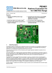
PE0201
CML Microcircuits
COMMUNICATION SEMICONDUCTORS
Platform Evaluation
Kit for CMX703x
Range
UM0201/5 February 2006
Features
• CMX703x FirmASICTM product range
evaluation
• Evaluate both RF and baseband
capabilities
• Command and control by PC via the PE0001
interface card or user’s µC development
application or emulator
• On-board 460MHz VCO
• Socketed EEPROM option for Function
ImageTM
• On-board supply regulators operate from a
single 5 volt supply
• On-board access to all CMX703x signals,
commands and data
1.
Brief Description
The PE0201 Platform Evaluation Kit is designed to assist in the evaluation and application development
of the CMX703x range of FirmASICTM products. The kit is in the form of a populated PCB comprising a
CMX703x IC and appropriate supporting components and circuitry, including a 460MHz VCO operating in
conjunction with one of the IC's on-chip synthesizers.
The board also incorporates all the necessary power-supply regulation facilities for operation from a
single 5 volt supply, together with a number of board jumpers to enable various circuit arrangements to be
effected.
The board is fitted with connectors allowing the PE0201 to be operated with a CML PE0001 Interface
Card and associated PC GUI software, or by direct connection between the CMX703x C-BUS serial port
and the user's µC development application or emulation system.
The CMX703x Function ImageTM (FI) can be loaded, on power-up, directly into the on-board target
CMX703x IC using the PE0001 interface or the user's system. Alternatively, it can be pre-loaded,
© 2006 CML Microsystems Plc
PE0201 Evaluation Kit
PE0201
separately, into the on-board EEPROM for automatic operation on power-up. Function images can be
downloaded from the CML website.
CONTENTS
Section
Page
1
Brief Description ..................................................................................... 1
2.
Preliminary Information.......................................................................... 4
2.1
Laboratory Equipment............................................................... 4
2.2
Precautions................................................................................. 4
2.3
Approvals.................................................................................... 4
3.
Quick Start ............................................................................................... 5
3.1
With PE0001................................................................................ 5
3.2
Without PE0001.......................................................................... 6
4.
Signal Lists .............................................................................................. 7
5.
Circuit Schematics and Board Layouts.............................................. 11
6.
Detailed Description ............................................................................. 12
6.1
Hardware Description.............................................................. 12
6.2
Adjustments and Controls ...................................................... 13
6.3
Function ImageTM ................................................................... 14
6.4
Evaluation Tests ...................................................................... 14
7.
Performance Specification................................................................... 17
7.1
Electrical Performance ............................................................ 17
It is always recommended that you check for the latest product datasheet version from the
Datasheets page of the CML website: [www.cmlmicro.com].
© 2006 CML Microsystems Plc
2
UM0201/5
PE0201 Evaluation Kit
PE0201
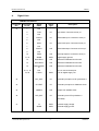
Auxiliary
connections
J11
Clocks
19.2MHz default
Baseband
connections
C-BUS
and Boot
control
CMX703x
J1
J10
EEPROM
+3v3D +3v3A
+3v3VCO
Supplies
VCO
450-470MHz
460MHz
Vin, J7
Figure 1 Block Diagram
© 2006 CML Microsystems Plc
3
UM0201/5
PE0201 Evaluation Kit
2.
PE0201
Preliminary Information
The CMX703x device fitted to the PE0201 has very little inherent functionality. The functionality
must come from a Function ImageTM which is downloaded from the CML website. The PE0201 is
designed to support a range of CMX703x FirmASICTM devices with their respective function
images. Not all features of the PE0201 will be available with a given Function ImageTM.
2.1
Laboratory Equipment
The following laboratory equipment is needed to use this evaluation kit:
A 5 Volt dc regulated power supply.
If being used with the PE0001 Interface Card the following items will also be required.
1. An IBM compatible PC equipped with a serial port and with one of the following Microsoft
operating systems installed - 98, NT, 2000sp4 or XP.
2. Software application ES000110.exe, or later version, installed on the PC.
3. RS232, 9-way DTE <-> DCE cable.
2.2
Precautions
Like most evaluation kits, this product is designed for use in office and laboratory environments.
The following practices will help ensure its proper operation:
2.2.1
Static Protection
This product uses low power CMOS circuits which can be damaged by electrostatic discharge.
Partially damaged circuits can function erroneously, leading to misleading results. Observe ESD
precautions at all times when handling this product.
2.2.2
Contents - Unpacking
Please ensure that you have received all of the items listed on the separate information sheet
(EK0201) and notify CML within 7 working days if the delivery is incomplete.
2.3
Approvals
This product is not approved to any EMC or other regulatory standard. Users are advised
to observe local statutory requirements, which may apply to this product and the radio
frequency signals that may emanate from it.
© 2006 CML Microsystems Plc
4
UM0201/5
PE0201 Evaluation Kit
3.
PE0201
Quick Start
This section is divided into two sub-sections. The first is for those users who are using the
PE0201 with a PE0001 controller card and its Windows PC application The second is for users
who are using the PE0201 by itself, without the PE0001.
3.1
With PE0001
Note that the C-BUS connector J1, a right angle header, of the PE0201 is designed to plug
directly into socket J1 of the PE0001.
3.1.1
Setting-Up
•
•
Ensure that all pins of header, J9, are open circuit.
Refer to the PE0001 user manual, and follow the instructions given in the quick start section.
The basic arrangement, when used with the PE0001 is shown below.
PE0201
J9
J7
Power
Supply
Direct Connection
J1
PE0001
J2
Serial Cable
PC
Figure 2 PE0201 used with PE0001
© 2006 CML Microsystems Plc
5
UM0201/5
PE0201 Evaluation Kit
3.1.2
PE0201
Operation
The Function ImageTM (FI) must now be downloaded to the CMX703x device. Use the ‘Function
Image Download’ tab of the PE0001 windows application. Two methods are available for
downloading the FI:
•
Directly from a file on the PE0001 host PC to the CMX703x.
•
From the PE0201 EEPROM. To use this method the EEPROM must first be programmed
with the FI using a user-supplied proprietary programmer. The EEPROM is socketed so that it
can be removed for this purpose.
Function images are available as a ‘C’ type header file and must be obtained from the CML
website.
The PE0201 should now be ready for evaluation of the CMX703x with the loaded FI.
3.2
Without PE0001
As an alternative to using the PE0001 controller kit, users may control the CMX703x target device
with a user-supplied host controller card. C-BUS serial interface connections are made via
connector J1.
The power-up, or boot state of the CMX703x may be set using jumpers on header, J9. Consult
the relevant CMX703x documentation for valid modes. A jumper in-circuit on header, J9,
corresponds to a ‘1’ state on the boot pins.
A FI for the CMX703x device must be either, included in the customers host system and
downloaded to the CMX703x device on power-up, or, programmed into the EEPROM using a
user-supplied proprietary programmer. The EEPROM is socketed so that it can be removed for
this purpose.
© 2006 CML Microsystems Plc
6
UM0201/5
PE0201 Evaluation Kit
4.
PE0201
Signal Lists
CONNECTOR PINOUT
Connector
Ref.
Connector
Pin No.
Signal
Name
Signal
Type
J1
1
N/C
-
2
CSN
I/P
3
N/C
-
4
CDATA
I/P
5
N/C
-
6
SCLK
I/P
7
N/C
-
8
RDATA
O/P
9
N/C
-
10
IRQN
O/P
11, 12
GNDD
PWR
13
BOOTEN1
O/P
CMX703x Hardware Boot Control.
14
BOOTEN2
O/P
CMX703x Hardware Boot Control.
15
RS232/CBUS
N
O/P
CMX703x Hardware Boot Control.
16, 17, 18
N/C
-
Do not connect these pins.
19, 20
+3V3D
PWR
3.3V dc digital supply rail.
J2
RF1_EXT
I/P
External input option to RF synthesiser 1.
J3
CLK EXT
I/P
External input option for CMX703x clock.
J5
460MHz
O/P
Output from 460MHz VCO.
J6
RF2_EXT
I/P
External input to RF synthesiser 2
Description
Chip select. Connects to host µC.
Serial Data input. Connects to host µC.
Serial clock input. Connects to host µC.
Serial data output. Connects to host µC.
Interrupt request. Connects to host µC.
Digital supply ground.
(not fitted).
J7
© 2006 CML Microsystems Plc
+V
PWR
External supply voltage.
GNDD
PWR
External supply ground.
7
UM0201/5
PE0201 Evaluation Kit
PE0201
CONNECTOR PINOUT
Connector
Ref.
Connector
Pin No.
Signal
Name
Signal
Type
J8
1
N/C
-
2
TXD
O/P
9-pin D Type connector – PC TXD.
3
RXD
I/P
9-pin D Type connector – PC RXD.
4
N/C
-
5
GNDD
Power
6
N/C
-
7
RTS
I/P
9-pin D Type connector – PC RTS.
8
CTS
O/P
9-pin D Type connector - PC CTS.
9
N/C
-
1
IP1
I/P
Channel 1 inverting input.
3
IP2
I/P
Channel 2 inverting input.
5
IP3
I/P
Channel 3 inverting input.
7
MOD1
O/P
Channel 1 output.
9
MOD2
O/P
Channel 2 output.
11
AUDIO
O/P
Channel 3 output.
13
BUF1IN
I/P
High impedance buffered input.
15
BUF1OUT
O/P
Buffered output.
17
BUF2IN
I/P
High impedance buffered input.
19
BUF2OUT
O/P
Buffered output.
2, 4, 6, 8,
10, 12, 14,
16, 18, 20
GNDA
PWR
Analogue supply ground.
1
AUXADC4
I/P
Auxiliary ADC input.
2
AUXDAC1
O/P
Auxiliary DAC output.
3
AUXADC3
I/P
Auxiliary ADC input.
4
AUXDAC2
O/P
Auxiliary DAC output.
5
AUXADC2
I/P
Auxiliary ADC input.
6
AUXDAC3
O/P
Auxiliary DAC output.
7
AUXADC1
I/P
Auxiliary ADC input.
8
AUXDAC4
O/P
Auxiliary DAC output.
J10
J11
© 2006 CML Microsystems Plc
8
Description
9-pin D Type connector – PC GND.
UM0201/5
PE0201 Evaluation Kit
PE0201
CONNECTOR PINOUT
Connector
Ref.
Connector
Pin No.
Signal
Name
Signal
Type
9, 10
GNDA
PWR
Analogue supply ground.
11, 12
N/C
13, 14
GNDD
PWR
Digital supply ground.
15, 16, 17,
18
N/C
-
19
GPIO2
BI
General purpose I/O pin.
20
GPIO1
BI
General purpose I/O pin.
Description
Do not connect these pins.
TEST POINTS
Test Point
Ref.
Default
Measurement
TP1
-
CMX703x system clock 1 output.
TP2
-
CMX703x system clock 2 output.
TP3
-
CP1OUT, charge pump output for RF synthesiser 1.
TP4
-
CP2OUT, charge pump output for RF synthesiser 2 (not fitted).
TP5
3.3V
Output from on-board regulator. DC supply voltage for analogue rail.
TP6
3.3V
Output from on-board regulator. DC supply voltage for digital rail.
TP7
3.3V
Output from on-board regulator. DC supply voltage for RF Charge
Pump and 460MHz VCO.
TP8
0V
GNDD, digital ground.
TP9
0V
GNDD, digital ground.
TP10
0V
GNDA, analogue ground.
TP11
0V
GNDA, analogue ground.
© 2006 CML Microsystems Plc
Description
9
UM0201/5
PE0201 Evaluation Kit
PE0201
JUMPERS/LINKS
Link
Ref.
Positions
Default
Position
JP1
1-2
short
Isolates analogue supply rail from CMX703x.
JP2
1-2
short
Isolates charge pump supply rail from CMX703x.
JP3
1-2
short
Isolates digital supply rail from CMX703x.
JP4
1-2
open
Write protects EEPROM (when shorted).
J4
1-2
short
19.2MHz TXCO clock source.
3-4
open
External clock source.
5-6
open
Crystal clock source – if components fitted by customer.
7-8
short
Ground external clock input.
9-10
open
Crystal clock source – if components fitted by customer.
1-2
open
Manual C-BUS (open) or RS232 selection (short).
3-4
open
Manual BootEn1 control (short = HI).
5-6
open
Manual BootEn2 control (short = HI).
13-14
short
Ground input to uncommitted buffer1.
17-18
short
Ground input to uncommitted buffer2.
J9
J10
Description
LEDs
LED Ref.
D16
Description
Indicates that digital supply voltage is present.
Notes: I/P
O/P
BI
N/C
PWR
© 2006 CML Microsystems Plc
=
=
=
=
=
Input
Output
Bidirectional
Not connected
Power supply connection
10
UM0201/5
TP8
+
C60
GNDD
TP9
GNDD
J1
R45
U8
TP6
U11
BOOTEN2
BOOTEN1
+
+
U7
D2
J7
D3
R41
+ 5V
L7
C59
C57
+
+
Board Mod
1 2 3 4
TP5
C55
C79 U9
TP7
+
U10
PE0201
C68
C65
J9
0V
R43
C62
C61
R20
U4
C31 R19
R18
C41
TR1
RF1_EXT
J2
R27
R13
U2
JP4
R52
CLKOUT2 TP2
C66 R21
R44
L8
R22
C67
C33
C64
U1
R4 TP1
JP3
J4
R15
L5
L4
R24
C40
C47
C48
R34
C46
R33
TR3
C44 R35
D1
R32
C45
TP3
C27
C28 L6
C74
C4
JP1
R36
C29
C24
C23
JP2
C2
+
C20
R48 R47
R1
C6
J6
R25
C37
C49
R23
C38
L3
C42
U6
CP1OUT RF2_EXT
R12 R11
C25
L1
R16
C1
C5
C16
C3
CLKOUT1C26
C14
X1
U3 C35
U5
C32
C34
CLK
EXT J3
TR2
C63
C36
J8
C43
R30
R17
C15
C71
R10
C7
+
C30
R37
C78
+
11
C56
R14
C10
C51
C50
R38
C9
C52
C69
R46
C17
R5
C53
C72
C8
C11
R2
R7
C39
R8
R3
TP4
R29
R31
R26
R28
C77
C21
C75
C13
C22
R51
C73
J5
GNDA
TP10
GNDA
TP11
J10
460MHz
CP2OUT
C54
L2
C70
R9
R50
C12
U12
C18
R6
C19
+
R39
+
© 2006 CML Microsystems Plc
C58
R49
5.
C76
J11
PE0201 Evaluation Kit
PE0201
Circuit Schematics and Board Layouts
For clarity, circuit schematics are available as a separate high resolution pdf file. This can be
found on the CML website.
+
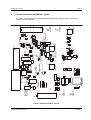
Figure 3 Evaluation Board - Layout
UM0201/5
PE0201 Evaluation Kit
PE0201
6.
Detailed Description
6.1
Hardware Description
6.1.1
Power supplies
The board is fitted with three voltage regulators. U7, U8 and U9 provide the analogue, digital and
RF Charge Pump supply rails respectively. The input to these three regulators is provided by an
external 5V dc regulated power supply, which is connected to the board via connector J7, a snap
type connector.
The Analogue, Digital and RF Charge Pump supply voltage levels can be monitored on test
points TP5, TP6 and TP7 respectively.
LED illumination confirms the on-board presence of the +3.3V dc digital voltage supply.
6.1.2
Clock Options
The PCB is designed to provide three CMX703x device clock options. The board is supplied with
a 19.2MHz oscillator module fitted. This option allows convenient RF synthesiser configuration to
typical channel spacings. If a FI providing an auxiliary DAC at AuxDAC4 is used, then fine tuning
of the output frequency is possible. A 3.9kΩ resistor should be fitted in position R21 for this
purpose.
Other options are an external clock source at J3 and PCB footprints for assembly of a quartz
crystal oscillator circuit (C34, C35 and X1).
Header J4 is used with jumper sockets to select the required option as shown in the table below.
Shaded cells illustrate locations where a jumper socket should be fitted.
J4
Jumper
position
1->2
3->4
5->6
7->8
9->10
Clock option
19.2MHz TCXO
(default)
External
Quartz crystal
Table 1 Clock Select Jumper Positions.
6.1.3
Control Interface
The C-BUS and CMX703x boot control signals are brought out on connector J1. This is a right
angle male header designed to plug directly into the PE0001 controller card which has a matching
female header. Additionally this connector carries the +3.3V digital supply rail, which can be used
to power the PE0001 card.
Alternatively, if not using the PE0001, the CMX703x boot control signals can be manually set with
jumpers on header J9.
© 2006 CML Microsystems Plc
12
UM0201/5
PE0201 Evaluation Kit
PE0201
It is possible that a future CMX703x device will have an RS232 interface instead of a C-BUS
interface. In such cases, the PE0201 will not operate with the PE0001 controller kit; the RS232
interface provided on the PE0201 PCB should be used instead.
6.1.4
Baseband Interfacing
Connector J11 provides access to Auxiliary ADCs 1 to 4, Auxiliary DACs 1 to 4, and the general
purpose I/O lines of the CMX703x device.
The CMX703x device baseband input amplifiers for IP1, IP2 and IP3 are configured as AC
coupled, unity gain, inverting amplifiers. The inputs to these circuits are fed from connector J10.
The CMX703x device baseband outputs, MOD1, MOD2 and AUDIO, are fed through an RC
network to connector J10.
A dual op amp IC is fitted to the board, with both amplifiers configured as unity-gain buffers. It is
possible to set up other op amp based configurations with the addition of passive components to
the PCB footprints provided. It is recommended that 0603 sized surface mount components are
used. Access to the input and output of each of these uncommitted amplifiers is also from
connector J10.
6.1.5
RF Circuits
The board is fitted with a Voltage Controlled Oscillator (VCO). Using RF synthesiser 1 of the
CMX703x device, the VCO is tuneable across a range of 450 to 470MHz, with a nominal
frequency of 460MHz. The output of the VCO is fed to connector J5, which is a straight SMA type.
The charge pump settings for CMX703x (RF channel control register, $B3), when using this VCO
should be:
Positive slope - $B3;b4=0.
High gain - $B;b3=1;
For further information, refer to relevant CMX703x data sheet.
Alternatively, RF synthesiser 1 can be used with an external VCO, with the following circuit
changes:
• Remove R11 and R28 - Disconnect VCO output from CMX703x.
• Remove R32 – Stops the on-board VCO oscillating.
• Remove R15 – Disconnect CMX703x charge pump output from on-board VCO.
The charge pump output of RF synthesiser 1 can now be picked up from TP3, labelled CP1OUT,
and the users VCO output connected to the SMA connector J2, labelled RF1_EXT. Note that the
loop filter for RF synthesiser 1 is still in circuit.
RF synthesiser 2 can also be used with a user-supplied external VCO. A loop filter can be
constructed using the PCB footprints provided. Also, the ISET resistor, R38, must be fitted. The
user-supplied VCO can be fitted across the following connectors that are not fitted:
• J6, SMA socket, labelled RF2_EXT – RF input to RF synthesiser 2.
• TP4, test loop, labelled CP2OUT – Charge pump output.
6.2
Adjustments and Controls
The boot state of the CMX703x device can be set manually, using jumpers on header, J9. If using
with the PE0001.
© 2006 CML Microsystems Plc
13
UM0201/5
PE0201 Evaluation Kit
6.3
PE0201
Function ImageTM
The PE0201 is shipped with a blank EEPROM, U2. The EEPROM is socketed, allowing it to be
removed and externally programmed with a FI. Instead of using the EEPROM, FIs may be
downloaded into the CMX703x device via the C-BUS interface.
Whenever power is removed from the PE0201 the FI will be erased from the CMX703x device.
Therefore, whenever power is applied a FI must be loaded, either from the EEPROM or via the CBUS interface.
6.4
Evaluation Tests
Before a FI is loaded into the CMX703x device, there is a limited functionality which can be
demonstrated directly by programming the C-BUS. The first group of examples can be used to
verify control of the CMX703x via the C-BUS serial interface.
All of the following examples are available as PE0001 compatible script files from the CML
website.
6.4.1
Write to and Read from a Register
•
Write any 16-bit number to register $C0.
The data transferred to the device on the Command Data pin looks like this:
{ C0 } { <ms byte> } { <ls byte> }
..... Command Data
•
The value written to this register (the Powerdown Control register) can be read back from
register $C4 by issuing a single command byte, then reading two data bytes from the Reply
Data pin, as follows:
{ C4 }
..... Command Data
{ <ms byte> } { <ls byte> }
..... Reply Data
Note that the power consumption of the device will increase once this register has been written to,
since some parts of the device will no longer be powersaved.
6.4.2
Check Analogue Path and Set Input Gain
Write 0x4061 to $C0 (Powerdown Control)
Write 0x0C30 to $B1 (Input Gain and Signal Routing)
Write 0x0008 to $CF (Test Mode)
Apply a 1kHz, audio signal to the input, IP3 (J10 pin 5), at a level of -10dBm (the maximum signal
level before distortion is about +1dBm.
Check the audio signal coming out of the AUDIO OUT pin (J10, pin 11). The level should be
5.5dB, below the level of the input signal.
The MOD1 and MOD2 outputs should have no signal on them. All three outputs should have a dc
bias level of approximately 1.65 volts.
© 2006 CML Microsystems Plc
14
UM0201/5
PE0201 Evaluation Kit
6.4.3
PE0201
Check Analogue Path and Set Output Gain
Write 0x03E1 to $C0 (Powerdown Control)
Write 0x410C to $B0 (Analogue Gain)
Write 0x0001 to $CF (Test Mode)
Apply a differential 1kHz, audio signal across the inputs, IP1 (J10, pin 1) and IP2 (J10, pin 2), at
a level of 0dBm between them.
Check the audio signal coming out of the AUDIO OUT pin (J10, pin 11). The level should be
-9.6dBm.
Check the audio signal coming out of the MOD1 pin (J10, pin 7). The level should be -6.0dBm.
Check the audio signal coming out of the MOD2 pin (J10, pin 9). The level should be -12.0dBm.
All three outputs should have a DC bias level of approximately 1.65 volts.
6.4.4
Generate Two External Digital Clocks
Write 0x0021 to $C0 (Powerdown Control)
Write 0x2577 to $AB (System Clock 1 PLL Configuration)
Write 0xE0C8 to $AC (System Clock 1 Reference and Source Configuration)
Write 0x09A0 to $AD (System Clock 2 PLL Configuration)
Write 0xE0C8 to $AE (System Clock 2 Reference and Source Configuration)
With the default 19.2MHz clock input, a digital clock frequency of 4.0MHz should be observed at
the AUX/SYS CLOCK 1 output, labelled CLKOUT1 (TP1), and a frequency of 19.968MHz should
be observed at the AUX/SYS CLOCK 2 output, labelled CLKOUT2 (TP2).
Now write 0xA0C8 to either $AC or $AE registers, to turn off the CLKOUT1 or CLKOUT2 outputs,
respectively.
6.4.5
Set RF Synthesiser 1
These settings will enable the on-board VCO to switch between two frequencies of 455MHz and
465MHz. The VCO output is monitored at SMA socket, J5, labelled 460MHz.
Each synthesiser has an N and an R value for the Rx frequency and the same again for the Tx
frequency. Once programmed, the synthesiser can easily be switched between Rx and Tx. An
Application Note is available separately, to help calculate the N and R values. The RF Channel
Data register ($B2) is used to program both RF synthesisers and this is done by 16 contiguous
writes to this register. This can be reduced to 8 contiguous writes if only one of the synthesisers
is to be programmed. There is no indication of the completion of these writes, except that the
synthesiser which has been written to will indicate lock in the RF Channel Status register ($B4),
once it has been enabled, and providing the correct external components have been used for the
programmed frequency. For this example, it is assumed that the RF frequency is derived from
the default clock frequency of 19.2MHz.
To select an Rx frequency of 465MHz and a Tx frequency of 455MHz on Channel 1 Synthesiser,
with a loop comparison frequency of 25kHz, the following values of N and R are required:
For 455MHz, using the Tx divider registers:
Tx N = 18,200 = 0x4718
Tx R =
768 = 0x0300
For 465MHz, using the Rx divider registers:
© 2006 CML Microsystems Plc
15
UM0201/5
PE0201 Evaluation Kit
PE0201
Rx N = 18,600 = 0x48A8
Rx R =
768 = 0x0300
Write 0x8000 to $B3 (RF Channel Control) to select XTAL clock input as reference.
Write 0x0021 to $C0 (Powerdown Control)
Write 0x4318 to $B2 (RF Channel Data, Tx N b9:0)
Write 0x4411 to $B2 (RF Channel Data, Tx N b19:10)
Write 0x4B00 to $B2 (RF Channel Data, Tx R b9:0)
Write 0x4C00 to $B2 (RF Channel Data, Tx R b19:10)
Write 0x50A8 to $B2 (RF Channel Data, Rx N b9:0)
Write 0x5412 to $B2 (RF Channel Data, Rx N b19:10)
Write 0x5B00 to $B2 (RF Channel Data, Rx R b9:0)
Write 0x5C00 to $B2 (RF Channel Data, Rx R b19:10)
Then:
Write 0x802D to $B3 (RF Channel Control) to select the Rx frequency or ...
Write 0x802B to $B3 (RF Channel Control) to select the Tx frequency or ...
Write 0x8028 to $B3 (RF Channel Control) to disable both Rx and Tx frequencies
When RF Synthesiser 1 is in lock, it will return the value 0x01 in the RF Channel Status register
($B4). When not in lock, this value will be 0x00. Depending on the setting of the IRQ mask in the
IRQ Mask register ($CE), an interrupt will be generated and the interrupt will be reported in the
Status 1 register ($C6) as the value 0x8002.
© 2006 CML Microsystems Plc
16
UM0201/5
PE0201 Evaluation Kit
7.
Performance Specification
7.1
Electrical Performance
PE0201
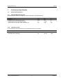
7.1.1 Absolute Maximum Ratings
Exceeding these maximum ratings can result in damage to the Evaluation Kit.
Min.
-0.3
-0.3
0
-20
Supply (VIN - VSS)
Voltage on any connector pin to VSS
Current into or out of VIN and VSS pins
Current into or out of any other connector pin
Max.
9.0
3.6
+0.45
+20
Units
V
V
A
mA
Max.
5.5
24.576
Units
V
MHz
7.1.2 Operating Limits
Correct operation of the Evaluation Kit outside these limits is not implied.
Notes
Supply (+V - VGND)
External Clock Frequency
© 2006 CML Microsystems Plc
17
Min.
4.5
4.0
UM0201/5
PE0201 Evaluation Kit
7.1.3
PE0201
Operating Characteristics
For the following conditions unless otherwise specified:
Evaluation Device Clock Frequency = 19.2MHz, VIN = 5.0V, Tamb = +25°C.
For CMX703x parameters, see relevant CMX703x data sheet.
DC Parameters
IDD
Notes
Min.
Typ.
Max.
Units
1
60
75
100
mA
3.15
3.15
3.15
3.3
3.3
3.3
3.45
3.45
3.45
V
V
V
2
4
-
100
0.1
-
kΩ
Ω
4
1
50
-
-
kΩ
MΩ
21
21
10
-
-
ns
ns
MΩ
450
-
6.5
50
470
-
MHz
dBm
Ω
+3V3A
+3V3D
+3V3_VCO
Baseband Parameters
Output Impedances
Mod1, Mod2 and Audio
Buf1out and Buf2out
Input Impedances
IP1, IP2 and IP3
Buf1in and Buf2in
External Clock Input
'High' pulse width
'Low' pulse width
Input impedance
3
3
VCO output
Frequency range
Power
Output Impedance
Notes:
1.
2.
3.
4.
Not including any current drawn from pins by external circuitry.
Small signal impedance.
Timing for an external input to the CLOCK/XTAL pin.
When configured, as supplied, as unity gain buffers.
© 2006 CML Microsystems Plc
18
UM0201/5
PE0201 Evaluation Kit
7.1.3
PE0201
Operating Characteristics - Timing Diagrams
See relevant CMX703x documentation for C-BUS signal timing information.
© 2006 CML Microsystems Plc
19
UM0201/5
PE0201 Evaluation Kit
PE0201
About FirmASIC™
CML’s proprietary FirmASIC™ component technology reduces cost, time to market and development risk,
with increased flexibility for the designer and end application. FirmASIC™ combines Analogue, Digital,
Firmware and Memory technologies in a single silicon platform that can be focused to deliver the right
feature mix, performance and price for a target application family. Specific functions of a FirmASIC™
device are determined by uploading its Function Image™ during device initialization. New Function
Images™ may be later provided to supplement and enhance device functions, expanding or modifying
end-product features without the need for expensive and time-consuming design changes. FirmASIC™
devices provide significant time to market and commercial benefits over Custom ASIC, Structured ASIC,
FPGA and DSP solutions. They may also be exclusively customised where security or intellectual
property issues prevent the use of Application Specific Standard Products (ASSP’s).
CML does not assume any responsibility for the use of any circuitry described. No IPR or circuit patent licences are implied.
CML reserves the right at any time without notice to change the said circuitry and any part of this product specification.
Evaluation kits and demonstration boards are supplied for the sole purpose of demonstrating the operation of CML products
and are supplied without warranty. They are intended for use in a laboratory environment only and are not for re-sale, enduse or incorporation into other equipments. Operation of these kits and boards outside a laboratory environment is not
permitted within the European Community. All software/firmware is supplied "as is" and is without warranty. It forms part of
the product supplied and is licensed for use only with this product, for the purpose of demonstrating the operation of CML
products. Whilst all reasonable efforts are made to ensure that software/firmware contained in this product is virus free, CML
accepts no resonsibility whatsoever for any contamination which results from using this product and the onus for checking
that the software/firmware is virus free is placed on the purchaser of this evaluation kit or development board.
www.cmlmicro.com
For FAQs see: www.cmlmicro.com/products/faqs/
For a full data sheet listing see: www.cmlmicro.com/products/datasheets/download.htm
For detailed application notes: www.cmlmicro.com/products/applications/
Oval Park, Langford,
Maldon, Essex,
CM9 6WG - England.
4800 Bethania Station Road,
Winston-Salem,
NC 27105 - USA.
No 2 Kallang Pudding Road,
#09 - 05/06 Mactech
Industrial Building,
Singapore 349307
No. 218, Tian Mu Road
West, Tower 1, Unit 1008,
Shanghai Kerry Everbright
City, Zhabei,
Shanghai 200070,
China.
Tel: +44 (0)1621 875500
Tel: +65 6745 0426
Fax: +44 (0)1621 875600
Tel: +1 336 744 5050,
800 638 5577
Fax: +1 336 744 5054
Fax: +65 6745 2917
Tel: +86 21 6317 4107
+86 21 6317 8916
Fax: +86 21 6317 0243
Sales:
[email protected]
Sales:
[email protected]
Sales:
[email protected]
Sales:
[email protected]
Technical Support:
[email protected]
Technical Support:
[email protected]
Technical Support:
[email protected]
Technical Support:
[email protected]