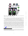
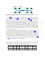
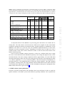
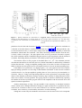
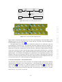
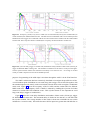
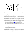
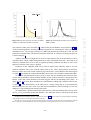
1
P UBLISHED BY I NSTITUTE OF P HYSICS P UBLISHING AND SISSA R ECEIVED : May 23, 2008 ACCEPTED : August 11, 2008 P UBLISHED : September 5, 2008 ATLAS Muon Drift Tube Electronics Y. Arai,g B. Ball, j M. Beretta,d H. Boterenbrood,k G.W. Brandenburg,c∗ F. Ceradini, f J.W. Chapman, j T. Dai, j C. Ferretti, j T. Fries,c J. Gregory, j J. Guimarães da Costa,c S. Harder,c E. Hazen,a J. Huth,c P.P.M. Jansweijer,k L.E. Kirsch,b A.C. König,l A. Lanza,e G. Mikenberg,m J. Oliver,c C. Posch,an R. Richter,i W. Riegler,co E. Spiriti, f F.E. Taylor,h J.C. Vermeulen,k B. Wadsworthh and T.A.M. Wijnenl University, Physics Department, Boston, MA, U.S.A. University, Department of Physics, Waltham, MA, U.S.A. c Harvard University, Laboratory for Particle Physics and Cosmology, Cambridge, MA, U.S.A. d INFN Laboratori Nazionali di Frascati, Frascati, Italy e INFN Pavia, Pavia, Italy f INFN Roma Tre and Università Roma Tre, Dipartimento di Fisica, Roma, Italy g KEK, High Energy Accelerator Research Organisation, Tsukuba, Japan h Massachusetts Institute of Technology, Laboratory for Nuclear Science, Cambridge, MA, U.S.A. i Max-Planck-Institut für Physik (Werner-Heisenberg-Institut), München, Germany j The University of Michigan, Department of Physics, Ann Arbor, MI, U.S.A. k Nikhef National Institute for Subatomic Physics, Amsterdam, Netherlands l Radboud University Nijmegen/Nikhef, Dept. of Exp. High Energy Physics, Nijmegen, Netherlands m The Weizmann Institute of Science, Department of Particle Physics, Rehovot, Israel n Now at the Austrian Research Center - ARC, Vienna, Austria o Now at CERN, Geneva, Switzerland E-mail: [email protected] b Brandeis A BSTRACT: This paper describes the electronics used for the ATLAS monitored drift tube (MDT) chambers. These chambers are the main component of the precision tracking system in the ATLAS muon spectrometer. The MDT detector system consists of 1,150 chambers containing a total of 354,000 drift tubes. It is capable of measuring the sagitta of muon tracks to an accuracy of 60 µ m, which corresponds to a momentum accuracy of about 10% at pT = 1 TeV. The design and performance of the MDT readout electronics as well as the electronics for controlling, monitoring and powering the detector will be discussed. These electronics have been extensively tested under simulated running conditions and have undergone radiation testing certifying them for more than 10 years of LHC operation. They are now installed on the ATLAS detector and are operating during cosmic ray commissioning runs. K EYWORDS : Electronic detector readout concepts (gas, liquid); Data acquisition circuits; Front-end electronics for detector readout; Detector control systems (detector and experiment monitoring and slow-control systems, architecture, hardware, algorithms, databases). ∗ Corresponding author. c 2008 IOP Publishing Ltd and SISSA http://www.iop.org/EJ/jinst/ 2008 JINST 3 P09001 a Boston Contents Introduction 1.1 The MDT precision tracker 1.2 The MDT drift tube 1.3 MDT readout system overview 1.4 MDT readout system optimization 1.5 MDT readout system data rates 2 2 4 6 9 11 2. MDT on-chamber electronics component design 2.1 Chamber interconnect boards 2.1.1 Front-end interconnect board (signal hedgehog) 2.1.2 On-chamber high-voltage distributor board (HV hedgehog) 2.2 Front-end electronics - the mezzanine board 2.2.1 Amplifier Shaper Discriminator (MDT-ASD chip) 2.2.2 Time to Digital Converter (AMT-3 chip) 2.3 On-chamber multiplexer - Chamber Service Module (CSM) 2.3.1 The passive interconnect 2.3.2 The active CSM multiplexer 2.4 Monitoring and control - Embedded Local Monitor Board (ELMB) 2.5 The calibration system 12 12 13 14 15 18 21 25 25 26 30 31 3. On-chamber electronics support services and environmental factors 3.1 Low-voltage power 3.2 High-voltage distribution 3.3 Radiation tolerance of the front-end components 3.3.1 Radiation levels in the MDT detector 3.3.2 Damage scenarios in electronics devices 3.3.3 Levels of test doses and test results 31 32 33 35 35 35 36 4. Off-chamber electronics - MDT Read Out Driver (MROD) 4.1 Functionality 4.2 Implementation 4.2.1 The MRODin FPGA 4.2.2 The MRODout FPGA 4.2.3 The busy signal 4.2.4 Configuration of the FPGAs 4.2.5 Software environment 4.2.6 Monitoring 4.3 Throughput tests 38 38 41 42 46 47 48 49 49 50 5. System tests 50 –1– 2008 JINST 3 P09001 1. 6. Conclusions 53 A. MDT chamber specifications 53 1. Introduction 1.1 The MDT precision tracker The muon spectrometer of the ATLAS detector is illustrated in figure 1. It is designed to detect charged particles exiting the barrel and end-cap calorimeters and to measure their momenta at polar angles greater than 7.7◦ corresponding to pseudo-rapidity |η | ≤ 2.7. The primary momentum measurement in the muon system is provided by monitored drift tube chambers (MDTs) which consist of pressurized drift tubes with a diameter of 30 mm, operating –2– 2008 JINST 3 P09001 The monitored drift tube (MDT) chambers are the main component of the precision tracking system in the ATLAS muon spectrometer [1]. The precisely manufactured MDT chambers are carefully monitored within the ATLAS detector for their position, internal deformations, and environmental conditions like temperature and magnetic field. Due to the combination of mechanical accuracy of each chamber and external position monitoring (“alignment”), the MDT system achieves a sagitta accuracy of 60 µ m, corresponding to a momentum resolution of about 10% at pT = 1 TeV/c. The 1,150 MDT chambers are made from 354,000 tubes and cover an area of 5,500 m2 . The main task of the readout electronics is to preserve the inherent measurement accuracy of the tubes (80 µ m) and to cope with the high hit rates expected at full LHC luminosity (up to 300 kHz per tube). In order to obtain the required tracking accuracy the front-end electronics have been implemented with a low-impedance, low-noise amplifier-shaper-discriminator (ASD) together with a high resolution TDC. To process the high data rates, the system architecture is based on fine segmentation of the readout (24 tubes per TDC), fast local processors, large storage capacities at each level of data processing and high-speed data links. The front-end electronics have also been designed to survive in a high radiation environment and have undergone testing certifying them for more than 10 years of LHC operation. In addition to reading out the MDT chambers, electronics are necessary to control the readout system, to monitor the chamber environment and running conditions, and to supply the necessary low and high voltage power. The organization of this paper is as follows. In the remainder of this section an overview of the MDT system is presented, which includes a summary of both the chamber mechanical design and the associated readout electronics. Section 2 contains a detailed discussion of the design of the onchamber electronics for reading out and monitoring the system, while section 3 covers the support services for their operation and the environmental factors that affect them. Section 4 describes the design and implementation of the off-chamber readout electronics. The final two sections discuss the testing of the system with cosmic rays and muon beams, and present some conclusions. An appendix is attached which tabulates the parameters of the individual MDT chambers for reference purposes. Electronics related to chamber alignment are not covered in this paper - see references [2] and [3] for the barrel and end-cap alignment systems respectively. with Ar/CO2 gas (93/7) at 3 bar. In the very forward region (2 < |η | < 2.7) of the innermost tracking layer cathode strip chambers (CSCs) are used due to their higher rate capability and time resolution [4]. Input to the Level-1 muon trigger [5], which selects muons pointing to the interaction region with transverse momenta above a programmable threshold, is provided by fast tracking detectors. These detectors are resistive plate chambers (RPCs) in the barrel region and thin gap chambers (TGCs) in the end-cap region [4]. Their time resolution guarantees the identification of the interaction bunch crossing, and their readout segmentation in the direction along the MDT wires measures the φ coordinate with a resolution of 1 cm. The MDT chambers are arranged in three layers along the trajectory of the track, which allows a determination of the momentum from the sagitta of the track’s curvature in the magnetic field. In the barrel part of the detector the three layers form coaxial cylinders, in the end-cap part they form large circular disks centered at the beam axis. In the inner MDT layer each chamber consists of eight tube layers which are segmented in two “multi-layers” of four tube layers each. In the middle and outer MDT layers the chambers consist of six tube layers divided into multi-layers of three tube layers. The multi-layers in a chamber are separated by a spacer for structural reasons as well as to permit a crude momentum measurement for low momentum tracks and the construction of a track segment for high momentum tracks. The distance between the multi-layers varies between 6 and 121 mm in the inner layer and between 170 and 317 mm in the middle and outer layers. MDT chambers are rectangular in the barrel and trapezoidal in the end-cap, being built in various dimensions to optimize solid angle coverage. Apart from the length, all MDT tubes are identical. In the final implementation, the MDT system will consist of 656 chambers in the barrel and 494 chambers in the end-caps. A detailed list of chamber types and dimensions is given in the –3– 2008 JINST 3 P09001 Figure 1. Cross-section of the muon system in a plane containing the beam axis. MDT chambers in the barrel (green) and in the end-cap (blue) are arranged in three layers around the hadronic calorimeters (red and grey). In the first layer of the end-cap, cathode strip chambers (yellow) are used near the beam-pipe instead of MDTs to cope with the expected high track densities at η ≥ 2.4. The chambers marked RPCs and TGCs are the trigger chambers in the barrel and end-cap regions. appendix in table 12 for the barrel and in table 13 for the end-cap chambers. Construction parameters of the different MDT chamber types and their locations in the detector are presented in [6]. With an average tube resolution of 80 µ m, a chamber resolution of 40 µ m and 35 µ m is achieved for 6 and 8 layer chambers, respectively. A detailed descriptions of the muon system is given in reference [4]. 1.2 The MDT drift tube Cathode tube µ Rmin In the Ar/CO2 gas the drift velocity shows a strong dependence on the radius, i.e. 10 µ m/ns close to the wall, 26 µ m/ns at Anode wire r = 7,25 mm and 52 µ m/ns close to the wire. The exact shape of the radius-to-drift time relation (r-t relation) depends on parameters like temperature, pressure, magnetic field and total hit 29.970 mm rate in the tube; the latter being due to field distortions caused by the positive ions. Figure 42 in section 5 displays an example Figure 2. MDT tube crossof the drift-time spectrum. In order to make optimal use of the section with ionisation clusters distributed along a track. inherent spatial resolution of the MDT tube, the r-t relation must be known with high accuracy, which is achieved by continuous calibration with tracks in the ATLAS experiment. The operating parameters of the MDT tubes are given in table 1. The main sources of the measurement error in the MDTs are diffusion and the uneven distribution of location and ionisation density of the primary clusters along the track. The electrons arriving earliest at the wire will in general come from a point along the track which is slightly displaced with respect to Rmin , leading to an increased travel time to the wire. The operation of the drift tubes at a pressure of three atmospheres reduces diffusion as well as the fluctuation of both ionisation and cluster location. A detailed discussion of the various physics contributions to the Table 1. Main MDT chamber parameters. Parameter Wire diameter Gas mixture Gas pressure Gas gain Wire potential Average drift velocity –4– Design value 50 µ m Ar/CO2 (93/7) 3 bar (absolute) 2 × 10⁴ 3080 V ∼ 20.7 µ m/ns 2008 JINST 3 P09001 Figure 2 shows the cross-section of a MDT tube. The wall thickness is 0.4 mm and the inner radius is 14.58 mm (Rmax ). For each track the electrons from the primary ionisation clusters drift to the central wire along radial lines, the corresponding drift lengths ranging from Rmin to Rmax . Figure 3. Main service connections to a MDT tube. At the high-voltage side the wire is terminated with the equivalent transmission line impedance of the tube (383 Ω) to avoid reflections. All contacts (round dots) between the chamber and the hedgehog boards are gold plated to ensure a long-term connectivity. • The rise time of the amplifier combined with the discriminator threshold, which determines the time needed to trigger the TDC. With the performance parameters of the electronics discussed below (see section 1.4) this contributes an average error of 20-25 µ m. This error can be further reduced if the charge in the leading edge is measured and a corresponding “slewing” correction is applied (see section 1.4). • The least significant bit (LSB) error of the TDC, which is 25 ns/32 = 0.78 ns, corresponding to an RMS-error of 0.23 ns. This contributes an average error of 20 µ m to the measurement of Rmin . In an MDT tube each track creates a sequence of pulses, the duration of which corresponds to the time difference in drifting from Rmin and Rmax . While only the electrons arriving earliest at the wire, namely those coming from the cluster created nearest to the anode wire (approximately from Rmin ), are used for the determination of the track coordinate, the subsequent ones will create additional threshold crossings, inflating the data volume to be read out. Therefore, the electronics have the capability to disable the discriminator for a certain time after the initial threshold crossing by means of a programmable dead-time. A detailed discussion of the time structure of the pulses is given in [9]. A schematic drawing of the MDT drift tube connections to the electrical services is shown in figure 3. At the right end is the high-voltage “hedgehog” board (section 2.1.2) where a 383 Ω resistor terminates the tube with its characteristic transmission line impedance and which also contains decoupling capacitors and protection components. The termination resistor suppresses signal reflection at the open end of the wire, however, it is also a significant source of thermal noise (see section 1.4). At the left end the signal hedgehog board (section 2.1.1) connects the tube to the “mezzanine” board (section 2.2) which contains the active readout electronics. An aluminum Faraday cage completely surrounds the electronics at both ends of the chamber to provide shielding from external noise sources. The metallic surface of each tube is grounded at both ends to the hedgehog boards and to the bottom plates of the Faraday cages, which are in turn –5– 2008 JINST 3 P09001 resolution is given in [7]. Though the work described in reference [7] was done for a different gas, the general results are also applicable to the Ar/CO2 gas [8]. The contribution from electronics to the drift time resolution is mainly due to two parameters: connected to the aluminum support structure of the chamber. The Faraday cages have undergone a chemical surface treatment (chromatisation) to assure a conductive, unalterable surface. A photograph of the readout end of an MDT chamber showing the location of the electronics components is shown in figure 4. Individual tube signals and grounds are carried via board-to-board connectors from the hedgehog board to the mezzanine board. Ground planes have been added on the top and bottom layers of the signal hedgehog board to shield the long signal traces on the board from the digital noise on the mezzanine boards. The two boards have also been separated by an aluminum inner wall of the Faraday cage (see figure 4), the so called “box-on-box” design. With this design excellent noise immunity has been achieved. 1.3 MDT readout system overview The architecture of the MDT readout is shown in figure 5. In the first stage, the raw signals from 24 tubes are routed via the signal hedgehog boards to the mezzanine boards where they are amplified, discriminated, and digitized. On the mezzanine board the signals from eight tubes are first processed by one of three custom-designed monolithic Amplifier/Shaper/Discriminator (ASD) chips. The binary differential signals output by the ASDs are then routed to the Time-to-Digital Converter (TDC) chip, where the arrival times of leading and trailing edges are stored in a buffer memory of 256 words. Each time measurement is paired together with an identifier of the corresponding tube. The time is measured in units of the Timing, Trigger and Control (TTC) clock of 40.08 MHz [10], which is the bunch crossing (BC) frequency of the LHC machine. There are 4096 bunches in a ma- –6– 2008 JINST 3 P09001 Figure 4. A photograph of the readout end of an end-cap MDT chamber where the assembly has been staged in sections to illustrate the tube ends with gas tubelets visible (upper center), one hedgehog board attached to the tube ends (upper right), one mezzanine board plugged through the inner Faraday cover (lower left), and a completely enclosed mezzanine board (lower right). In the center is the “chamber service module” (CSM) without its protective cover, and the red box to its left contains an “embedded local monitoring board” (ELMB). chine cycle, so the BC or “coarse time” is described by a 12 bit word. In the TDC the BC interval of 24.95 ns is subdivided by 32 via a Delay Locked Loop (DLL) resulting in a “fine time” period of 0.78 ns. This leads to an RMS timing error of 0.23 ns in measuring the arrival times. An additional programmable feature of the ASD is the measurement of the pulse height of the signal, which allows for the monitoring of the gas gain as well as for pulse height dependent “slewing” corrections to the timing. The pulse height is encoded as the time interval between the leading and trailing edge of the ASD output pulse, with an output pulse width of 150 ns corresponding to the maximum input pulse height to be recorded. With this feature enabled the trailing edge of the ASD output pulse does not depend on the discriminator status and the discriminator is disabled until after the pulse height encoding has safely elapsed. Additional discriminator dead-time is also programmable and can be increased up to 750 ns in order to mask multiple hits from the same track.1 The mezzanine board containing the TDC chip plus three ASD chips, and serving 24 tubes, is the basic readout element of the MDT chambers. MDT chambers contain up to 18 mezzanine boards which are controlled by a local processor, the Chamber Service Module (CSM), as shown in figure 5. The interconnection scheme between CSMs and mezzanine boards is illustrated in figure 6. High-density 40 pin twisted pair cables are used to transmit control signals as well as supply power. 1 For tracks passing near the wire there are ionisation clusters extending from the minimum to the maximum times corresponding to Rmin and Rmax respectively, and as a result the shaper circuit has to integrate a large amount of charge. When the shaper is finally “released” the signal may overshoot the baseline outside the dead time window resulting in increased noise at times greater than the maximum allowable. –7– 2008 JINST 3 P09001 Figure 5. Schematic diagram of the MDT readout electronics. Each CSM serves up to 18 mezzanine boards depending on chamber size, each MROD up to 6 CSMs. Figure 6. The CSM collects data from up to 18 mezzanine boards which serve 24 MDT tubes each. Data are transmitted via high-density twisted pair cables from the mezzanine boards to the CSM. Table 2. Modularity of the MDT readout electronics. The difference between the number of chambers and CSMs in the barrel is due to some CSMs serving a pair of chambers. The allocation of MRODs to the barrel or end-cap is approximate, some MRODs serving CSMs from both regions. Region Barrel Two endcaps Total Tubes 191568 162816 354384 ASDs 24114 20352 44466 Mezz. boards 8038 6784 14822 –8– CSMs 624 494 1118 Chambers 656 494 1150 MRODs 100 104 204 2008 JINST 3 P09001 JTAG [11] information is distributed by the detector control system (DCS) through a serial bus system called the CANbus [12], using the CANopen protocol [13]. Each chamber contains a CANbus node located on the Embedded Local Monitor Board (ELMB) [14] The ELMB executes the JTAG operations, loads configuration code into the CSM, and monitors temperature sensors and supply voltages on the CSM and mezzanine boards, as well as temperature and magnetic field values from sensors distributed over the chamber. The ELMB interfaces to the CSM via opto-couplers, such that there is no DC connection between the CSM/chamber ground and the CANbus wires. Programming of the CSM and of the ASD and TDC chips on each mezzanine board is done over JTAG, allowing for a string of 72 bits for the CSM, of 160 bits per three ASD chips and of 180 bits per TDC chip. In this way, many parameters and functions can be controlled, including the setting of the discriminator threshold and dead-time, triggering of test pulses for calibration, or deactivation of noisy channels. The CSM communicates with the off-chamber electronics via two fibers, one coming from the TTC distribution box and the other going to the MDT Readout Driver (MROD) [15]. During normal data taking, the CSM broadcasts the TTC control and trigger signals to the TDCs and collects the data coming from the TDCs in response to all the Level-1 triggers. Subsequently, the data are formatted, stored in a de-randomizing buffer, and sent via an optical link to the MROD in the USA15 service cavern. The MROD is a VME module, serving up to six CSMs. Its main task is to assemble the data associated with each event for rapid transfer to the Readout Buffer (ROB) [16] where data are stored until the event has been either accepted or rejected by the Level-2 trigger. Table 2 summarizes the modularity of the readout system. Table 3. Power consumption of components, a mezzanine board, an ”average” MDT, a ”maximum” MDT (with 18 mezzanine boards) and the overall system. An average MDT has a calculated 308 tubes, served by approximately 13 mezzanine boards. The current drawn by an average and a maximum MDT is 6.3 and 8.3 A respectively. The average consumption per tube is 82 mW excluding, and 93 mW including the cable loss. Mezz. mW 300 mW 900 360 90 1350 280 1630 count 3 1 1 MDT Chamber avg. max. W W 21.2 4.0 25.2 System 1150 ch’s kW 29.3 4.0 33.3 29 4 33 An important feature of the MROD is its processing power that allows it to monitor the incoming data. The data streams received from the CSMs can be sampled for tube and chamber occupancies and their deviations from nominal values, possibly pointing to a malfunction. As the MRODs see the full Level-1 event rate, they can accumulate significant statistics in a short time, allowing for an early recognition of errors. Depending on average event size and Level-1 rate, a variable fraction of the events will be monitored in order to not slow down data transfer to the ROBs, which has priority. Power for the on-chamber readout electronics is routed via a shielded cable from a single DC source to the CSM and is then distributed separately to the analog and digital circuitry on the mezzanine boards. The source voltage is adjusted to deliver approximately 4 V at the CSM. Each mezzanine board draws about 270 mA for the analog part and 140 mA for the digital part at about 4 V, which is regulated to 3.3 V by on-board regulators. Thus the total power consumption of a mezzanine board is 1.6 W, including the power used by the voltage regulators. The CSM, including its regulators, consumes about 4 W, a large chamber with mezzanine boards for 432 tubes consumes 33 W, and the entire MDT system consumes 37 kW. A breakdown of the power consumption of the MDT readout electronics is given in table 3. 1.4 MDT readout system optimization Extensive test-beam measurements and simulations have been performed in order to study the spatial resolution of the MDT system under different operating conditions and to optimize the –9– 2008 JINST 3 P09001 ASD AMT Drivers / Receivers Mezzanine board @ 3.3 V Voltage regulator 4 V ⇒ 3.3 V Mezzanine board @ 4 V MDT, excluding CSM CSM (1 A @ 4 V) Complete MDT at 4 V Total MDT (excl. supply cables) Supply cable loss (∼ 15%) Total MDT (incl. supply cables) Component Figure 8. Effect of the time-slewing corrections on the average spatial resolution of a the drift tubes. The maximum rate expected for the MDTs is ≤ 150 Hz/cm2 . parameters for the front-end electronics [17, 18]. As an example, figure 7 shows the resolution as a function of the drift distance at different background rates ([9, 19 – 21]). Background hits, due to converted neutrons and γ ’s, lead to space charge in the drift gas and, consequently, to drift field fluctuations which reduce the resolution. This effect, increasing with the distance from the wire, is clearly visible in the figure. The tube signals in the Ar/CO2 gas and the electronics response have been simulated with the GARFIELD program and are in good agreement with the measured resolution, illustrating that the performance of the MDT system is quite well understood. The baseline choice for the gas gain of the MDT tubes is 2 × 10⁴ . The minimum practical discriminator threshold is five times the noise level, which in the MDTs is dominated by termination resistor thermal noise. Using pre-amplifier peaking times of less than 5 ns does not improve the MDT resolution since the signal-to-noise ratio rapidly becomes worse for such short peaking times. If the MDTs were operated at a very high gas gain (> 105 ), the signal-to-noise ratio would be high, permitting operation at a wide range of discriminator thresholds. In that case the resolution would be best for very fast pre-amplifiers (peaking times of 3-4 ns) and very low thresholds (3-5 electrons). However, owing to the high background rates in the spectrometer, the possible degradation of the chamber performance (ageing) caused by large amounts of charge deposited on the anode wire would be a serious problem. The ageing effects are therefore minimized by operating the chamber at the lowest possible gas gain which is still compatible with the electronic noise and spatial resolution requirements. Another disadvantage of using a fast pre-amplifier is the sensitivity to individual ionisation clusters which causes multiple threshold crossings per signal and therefore a significant increase in the hit rate. Therefore a choice of a rise time of about 15 ns is the best compromise in terms of resolution, noise sensitivity, overall stability and choice of ASIC technology. Taking into account only the termination resistor noise, the five times noise level corresponds – 10 – 2008 JINST 3 P09001 Figure 7. Spatial resolution of a drift tube as a function of the drift distance r at various levels of γ -irradiation with a threshold of 16 photoelectrons (p.e.). 1.5 MDT readout system data rates The flow of data through the front-end is subject to the rate of hits in the MDT tubes and varies widely over the span of chambers. Estimates of the rates (with a safety factor of five) for chambers at small angles to the beam line and for the inner layers, approach saturation of the TDC processing capacity at 1034 cm−2 s−1 luminosity. The majority of the hits are not from muon tracks but from photon and neutron induced ionisation. The TDC is designed to remove old hits from its buffer when average tube rates exceed 300 kHz (see section 2.2.2). Table 4 displays the data flow rates from the TDC through the CSM. The ATLAS wide maximum trigger rate, 100 kHz, is used in the rate calculation along with an 800 ns TDC “search window” for each trigger. The maximum rate on the TDC-CSM link is 80 Mbit/s. Four different tube hit rates chosen for illustration. The 0 kHz value is included to show the bandwidth occupied by synchronization words (called headers and trailers) and mask words that flag prior hits. Each – 11 – 2008 JINST 3 P09001 to 17 primary electrons for the baseline gas gain. A detailed analysis of the current pre-amplifier design showed that trace capacitances on the board and other parasitic capacitances increase this threshold level to 22–25 electrons [22]. The change in resolution for different thresholds and peaking times is primarily due to time slewing corresponding to different signal rise times from charge fluctuations in the leading edge. By measuring the charge in the leading edge with a short gate ADC (gate time less than twice the peaking time), a correction for the time slewing can be made to improve the resolution [17]. Figure 8 shows the gain in resolution obtained by the slewing correction with little dependence on the background rate. At the maximum expected rate of 150 Hz/cm2 a resolution of 90 and 110 µ m is obtained with and without the correction. To avoid further loss in resolution caused by charge fluctuation, the discriminator time walk should be less than 500 ps (corresponding to an average position error of about 10 µ m) for the entire signal input range. To minimize the number of threshold crossings per track the discriminator has a programmable amount of hysteresis. For a gas gain of 2 × 10⁴ and a threshold of 24 electrons including some hysteresis, 1-2 threshold crossings per signal is typical for the standard tail cancellation with a two stage pole/zero filter used. In order to ignore unwanted secondary hits, the ASD can be operated in a programmable dead-time mode, suppressing trailing hits for a preset interval [23]. In case of a Level-1 trigger all accepted hits within the maximum drift time window are read out. If the pattern recognition algorithm finds a tube to be inefficient it is useful to know the reason for the inefficiency. Reading out the hits within a window preceding the actual drift time window allows one to determine whether an earlier hit (possibly caused by a γ -conversion) could have obscured the hit from the muon track. To minimize bandwidth requirements a single bit is set by the TDC to flag as pile-up the occurrence of any hits prior to the digitization window. The requirements on bandwidth, buffer memory in the TDC, and serial link speed are mainly determined by the background hit rates. According to detector simulations the maximum count rate per tube in the MDT system is 300 kHz (including a safety factor of five for the uncertainty in the background simulation). The options implemented in the ASD-TDC design for various quantities of interest (leading and trailing edges, integrated signal leading edge and multi-hit information) are discussed in the following sections. Table 4. The relationship between tube hit rates in kHz and the link occupancy at low, medium and high hit rates of the MDT tubes. A hit rate of 0 is included to illustrate the bandwidth occupied by TDC headers, trailers, and mask words. Ungated hit rate per tube [kHz] Gated tube hit rate Gated TDC hit rate Gated TDC word rate Gated TDC bit rate Fraction of TDC =⇒ CSM link Per 18 mezz board chamber Fraction of CSM =⇒ MROD link =⇒ [kHz] [kHz] [kHz] [Mbits/s] percentage [Mbits/s] percentage 0 75 0 0 300 10.8 13.5% 172.8 12.6% 6 144 588 21.2 26.5% 338.7 24.7% 150 12 288 876 31.5 39.4% 504.6 36.8% 300 24 576 1452 52.3 65.3% 836.4 61.0% 2. MDT on-chamber electronics component design The on-chamber electronics components consisting of the hedgehog boards, the mezzanine boards, the chamber service module (CSM), and the local monitor board (ELMB), are described in detail in this section. 2.1 Chamber interconnect boards At both ends of an MDT chamber there are interconnect (“hedgehog”) boards which passively terminate the drift tube wires with capacitors and resistors. At one end the signal hedgehog boards couple the tubes with the front-end readout electronics (section 2.2), while at the other end the high-voltage (HV) hedgehog boards connect the tubes to the high-voltage distribution system (sec- – 12 – 2008 JINST 3 P09001 TDC sends one each of these three words for each trigger. The first row of table 4 represents ungated hit rates. The remaining rows represent data selected for output by the trigger and gate width. The processing bandwidth of the CSM is designed to pass all incoming data. The removal of hits at high rates is left exclusively to the TDC where a flag is provided with each data word to indicate when prior hits were lost. Data flows from the CSM to the MROD over a 1.6 Gigabit/s link and consists of TDC output from up to 18 mezzanine boards, two optical synchronization words and one readout cycle synchronization word (see section 2.3.2). The available bandwidth for chamber data is thus reduced by an 18/21 ratio to 1.37 Gigabit/s. The rate of data transmission from CSM to MROD exceeds the sum of the total input rate from 18 mezzanine boards and yields a slightly lower percentage occupation in each case in the table. It should also be noted that the chambers in the regions with the highest rates have 16 or fewer mezzanine boards. See figure 34 for a more detailed evaluation of the expected data rates into the MRODs. Flow control within each MROD is provided by a ROD busy output, and a logical OR of all such busy signals inhibits triggers. The ROD busy design is an ATLAS wide feature and not exclusive to the muon system. tion 3.1). Each hedgehog board services 24 tubes. At each end of the chamber the hedgehog boards are enclosed in Faraday cages to shield the tube connections. 2.1.1 Front-end interconnect board (signal hedgehog) An example of a signal hedgehog board is shown in figure 9. For each tube this board contains both signal and ground receptacles together with a HV-decoupling capacitor and two resistors that form a protection network (see figure 14 in section 2.2). A mezzanine board plugs directly onto the pin headers of the hedgehog board. The signal hedgehog is a four-layer printed circuit board with the signal traces routed on the two internal layers. The two external layers are ground planes covering as much surface area as possible taking in consideration the necessary clearance around the HV receptacles. The ground planes are required to shield the signal traces from HF noise generated by the TDC clock on the mezzanine board. There are four different types of signal hedgehogs, two of each for the 3-layer and 4-layer MDT chambers respectively. For each kind of chamber the two types geometrically fit the shapes of the two multi-layers. The 3-layer boards have 8 channels (tubes) per layer and the 4-layer boards have 6 channels per layer, both totaling 24 channels. The board shown in figure 9 is for a 4-layer chamber. The HV-decoupling capacitor is a 470 pF, 6.3 kV ceramic capacitor produced by Murata. The same type is used in the HV hedgehogs. It is placed in series with the signal path, so the signal quality could possibly be degraded by its performance. For this reason, its stability was extensively tested under different HV, temperature and humidity conditions. Its mean failure rate has been measured to be 0.0004% per unit for every 1000 hours of operation [24]. Each of the 24 MDT tubes serviced by a signal hedgehog board is connected to a unique TDC channel on the attached mezzanine board, and the TDC channel number is the identifier for that – 13 – 2008 JINST 3 P09001 Figure 9. A signal hedgehog board for 4 tube layer chambers. Table 5. The mapping between the MDT tube location and the TDC channel number for the four signal hedgehog board types. The orientation and placement of the different hedgehog types depends on chamber type and location within the detector [25], [26]. Row 1 2 3 1 2 3 1 2 3 4 1 2 3 4 TDC Channel # for Tubes in Layer 1, 3, 5, 7, 6, 0, 4, 2 9, 11, 13, 15, 14, 8, 12, 10 17, 19, 21, 23, 22, 16, 20, 18 1, 3, 5, 7, 6, 4, 2, 0 9, 11, 13, 15, 14, 12, 10, 8 17, 19, 21, 23, 22, 20, 18, 16 5, 3, 4, 2, 0, 1 11, 9, 10, 8, 6, 7 17, 15, 16, 14, 12, 13 23, 21, 22, 20, 18, 19 3, 1, 5, 0, 2, 4 9, 7, 11, 6, 8, 10 15, 13, 17, 12, 14, 16 19, 21, 23, 18, 20, 22 tube in the output data stream. The mapping between tube location and TDC number is different for each hedgehog type and is given in table 5. The signal hedgehog boards are conformally coated with Dow Corning R4-3117 RTV. This eliminates leakage current between the traces as long as the relative humidity is less than approximately 50%. The insulation properties of this product were shown to be adequate after both neutron and gamma radiation. 2.1.2 On-chamber high-voltage distributor board (HV hedgehog) The distribution of high-voltage to the MDT tubes is done by the HV hedgehog board, which is mechanically interfaced with the tubes using the same receptacles as on the signal hedgehogs. The schematic of a single channel of this board is shown in figure 10. The combination of the 1 MΩ resistor and 470 pF capacitor filters the high-frequency noise (> 500 Hz) on the high-voltage line. In the case of a wire short the maximum HV supply current set on the distributors, which cannot be greater than 0.7 mA, will flow through the 1 MΩ resistor for a period of 0.1 seconds, after which time the HV will be shut off. The capacitor is the same type as described in the signal hedgehog section. The final component is the 383 Ω resistor, which is in series with the tube matching its impedance. As with the signal hedgehogs, there are 24 channels on each board, distributed in 3 rows of 8 channels each or in 4 rows of 6 channels each for the 3-layer and 4-layer chambers respectively. The layout is designed on two layers, without shielding layers, taking in account the minimum clearance of 3 mm between high-voltage and ground. The irregular design of some chamber Faraday cages plus the need for special HV hedgehogs that connect to the external HV source leads to a much – 14 – 2008 JINST 3 P09001 Type I (3-layer) " " II (3-layer) " " III (4-layer) " " " IV (4-layer) " " " 1 MΩ 383 Ω 1W 0.125 W HV+ Wire 470 pF Endplug Ground HV- Figure 10. Schematic of one HV hedgehog channel. larger number of board designs than in the case of the signal hedgehogs. The total number of HV hedgehog types is 28: 22 for the barrel and 6 for the end-cap. A typical 3-layer HV hedgehog for the barrel MDTs is shown in figure 11. The high-voltage lines coming from the external HV splitter box are connected to only one HV hedgehog for each multi-layer. This particular board has additional connectors installed: for the barrel chambers they are AMP two-position connectors, separated for high-voltage and ground, and for the end-cap they are Molex five-position connectors, with high-voltage and ground contacts on the same connector. In order to pass the high-voltage line through the full multi-layer, each highvoltage line on the hedgehogs is daisy-chained from board to board. In the barrel this is done using gilded jumpers. The end-cap HV hedgehogs are stepped due to the trapezoidal geometry of the chambers, and in this case chaining is done by means of wire jumpers connecting Molex multi-pin connectors on adjacent boards. Because of the high voltages present on the hedgehog boards, they are expected to operate in a relative humidity less than approximately 50%. 2.2 Front-end electronics - the mezzanine board The mezzanine board carries the active electronics for 24 MDT channels and comes in different configurations for chambers with 3 and 4 tube layers. A block diagram of the mezzanine board is shown in figure 12 and a picture of a 3 tube layer board is shown in figure 13. Three MDT-ASD chips, one TDC chip, two voltage regulators, LVDS-drivers/receivers, a temperature sensor, and various other components are mounted on the board. The dimensions of the boards for 3 (4) tube layers are 11.2 × 9.3 cm (11.2 x 10.9 cm). – 15 – 2008 JINST 3 P09001 Figure 11. A 3-layer barrel HV hedgehog board. ! "#$ ! %& )* *' ! '! ! *' ! '! ! +' , ! ! "'(( Figure 12. The mezzanine board contains three 8 channel ASD chips, a 24 channel time digitizer called the AMT, 3.3V power regulators, protection circuitry, connectors that accept the wire signals and a header for the cable to the readout logic. Figure 13. A mezzanine board for use on a three tube layer MDT chamber. The input protection circuitry is on the left, the three ASD chips in the middle, and the AMT chip plus the CSM cable connector are on the right. – 16 – 2008 JINST 3 P09001 +' Figure 14. The input protection components on both the hedgehog board and the mezzanine board limit the pulse current into the amplifier. – 17 – 2008 JINST 3 P09001 The chamber input signals are carried in groups of eight from the signal hedgehog boards. Extensive protection against damage from HV discharges in the tubes is provided in several stages as shown figure 14. The hedgehog board has a 10 Ω series through-hole 1/4 W resistor. It was found during testing that the inductance provided by the leads of the through-hole component was essential to limit the pulse current to the mezzanine board in the event of an HV breakdown. On the mezzanine board, there are two stages of series resistors and back-to-back diodes to ground. The 20 Ω value of the series resistors was chosen as a compromise between increased series noise and pulse current reduction. Finally, the MDT-ASD chip itself contains integral protection diodes to limit input transients. With this protection scheme the MDT electronics were demonstrated to be robust against an indefinite number of full HV discharges. Each ASD chip processes signals from eight MDT tubes, providing eight LVDS outputs to the TDC. These LVDS signals are also available on a small header on the mezzanine board for diagnostics. The TDC time-stamps the output pulses of the ASD using a clock and an encoded trigger, which are received serially on two LVDS pairs from the CSM. The output data and a strobe signal associated with these data are also carried on LVDS pairs between the TDC and CSM. Finally, a calibration pulse trigger signal is received from the CSM on an LVDS pair, and is buffered, and distributed to the ASDs by the TDC. The programmable parameters for both the ASD and the TDC are initialized using the JTAG protocol. The three ASDs on each mezzanine board are connected in daisy-chain fashion, and are controlled by interface logic on the TDC. The TDC in turn is connected to a JTAG port controlled by the CSM. A shielded ribbon cable with 20 twisted pairs connects the mezzanine board with the CSM transmitting the digital signals discussed above. A list of the cable lines is given in table 6. In addition to the digital data, four pairs of the cable are used to supply analog power to the mezzanine board and three separate pairs are used to for digital power. The cable also carries both voltage read lines and the signal from a TMP37 [27] linear temperature sensor on the mezzanine. These are digitized by ADCs on the CSM. The analog and digital supply voltages AVddin and DVddin are supplied by a common source on the CSM. However, to minimize noise the corresponding grounds are kept separate, including separate ground planes for the digital and analog portions of the mezzanine board. Both analog and digital input power are each protected by a 1.5 A fuse and regulated at 3.3 V by an LP3964-3.3 linear voltage regulator [28]. The currents for the analog and digital supplies are 0.27 and 0.13 A, yielding a total consumption of 1.6 W at 4 V (for more detail on the power consumption see table 3 in section 1.3). Table 6. Pin allocation of the mezzanine board. The resistance of the 40-wire cable is 0.32 Ω/m per wire. Cable lengths on most MDT chambers range from 0.33 m to 1.33 m. If CSMs are located outside the chamber (e.g. BIS, BEE) cable lengths run up to 5 m. function AVddin (4 V); analog ground calibration strobe input to ASDs temperature sensor; analog ground regulated analog volt. (3.3V); anlg. grd. regulated digital volt. (3.3V); dig. grd. DVddin (4 V); digital ground master reset; digital ground serial data out from AMT system clock input to AMT encoded control input to AMT serial strobe out from AMT JTAG TMS JTAG TCK JTAG TDI JTAG TDO signal DC LVDS DC DC DC DC CMOS LVDS LVDS LVDS LVDS CMOS CMOS CMOS CMOS destination AVdd reg. ASDs CSM CSM CSM DVdd reg. AMT CSM AMT AMT CSM AMT AMT AMT CSM Threshold 1 of 8 Channels Discriminator Preamp Leading Edge Diff Amp Shaping Amp MDT 1 Trailing Edge LVDS Logic ADC 2 Charge Calibration System Control Logic (JTAG Interface) Figure 15. Block diagram of one ASD channel. 2.2.1 Amplifier Shaper Discriminator (MDT-ASD chip) A block diagram of one of the eight channels in the MDT-ASD chip [29] is shown in figure 15 and its specifications are listed in table 7. Each channel consists of a differential input stage, a tail cancellation shaper, a discriminator, a gated integrator, output control logic and an LVDS output driver all running within a 3.3V supply. The input stage is a pair of low noise cascode pre-amplifiers of moderately low input impedance (<100 Ω) for efficient charge collection from the relatively high impedance (383 Ω) MDTs. The – 18 – 2008 JINST 3 P09001 pin number 1, 3, 5, 7 2, 4, 6, 8 9 10 11 12 13 14 15 16 17, 19, 21 18, 20, 22 23 24 25 26 27 28 29 30 31 32 33 34 35 36 37 38 39 40 Table 7. ASD specifications. Power supply Pre-amplifier input impedance Pre-amplifier noise resistance Discriminator time walk Pre-amplifier peaking time Power consumption Channels per chip Minimum pulse spacing of ASD output 3.3 V 100 Ω < 100 Ω < 500 ps for the entire input signal range approximately 5 ns 30 mW per channel → 240 mW per chip 8 10 ns Vb4 M4 Vb3 M3 M2 R1 Vb2 Cf OUT R2 IN M1 Vb1 Figure 16. Cascode pre-amplifier schematic. pre-amplifier shown in figure 16 is a low-noise design such that the noise of the system is dominated by the terminating resistor at the far end of the drift tube. The differential input provides high common-mode rejection of noise pick up at the input. The tail cancellation shaper is a two-stage pole/zero network, which also provides the gain necessary at the discriminator input. Each pole/zero stage is characterized by a pole/zero ratio, which is fixed by design, and a single programmable time constant. Thus changes in drift gas composition can be accommodated within certain limits. In response to a delta function test pulse, the signal peaking time at the discriminator input is in the range of 10-12 ns. The discriminator is a three-stage design with programmable hysteresis as shown in figure 17. The shaper output is AC-coupled onto the differential pair (M1, M2). Two current mirror "loops" provide differential outputs, which are converted to low-impedance outputs by inverters at OUTa and OUTb. Positive feedback is provided by pair (M1a, M2a) with a programmable current source (I2) which allows for adjustable hysteresis. This design provides fast switching and a time walk which is <500 ps over the dynamic range of the MDT signals. The gated integrator is controlled by a one-shot which is initiated by the switching of the discriminator and covers the leading edge of the pulse. The charge contained in the leading edge is stored on a capacitor and then run down by the usual Wilkinson technique. The gate width is of – 19 – 2008 JINST 3 P09001 Vdd Vdd OUTb M1a OUTa M2a INa INb M1 M2 I1 I2 GND Figure 17. CMOS discriminator with programmable hysteresis. order 8-45 ns and the rundown of order 100 ns to provide approximately seven bits of resolution. This time-encoded charge is used off-line as a correction for time slewing and enhances the leadingedge spatial resolution by about 20 µ m, as shown in figure 8. The output logic block shown in figure 15 provides two modes of operation. The first mode is time-over-threshold (TOT mode) where the output logic signal is forced high as long as the MDT shaped signal is above a fixed threshold. Ideally, this starts on arrival of the first few electrons at the anode wire and ends shortly after the last electrons arrive from the tube wall. In practice, the clumpiness of the primary ionization results in multiple crossings of the discriminator during this time. In the second mode of operation (ADC mode) the fixed current rundown of the charge on the capacitor of the Wilkinson integrator determines the width of the output pulse. The criteria for selecting one of the two options are the following: • At the start-up of the experiment when data rates are low, the leading and trailing edges (TOT mode) can be used. The correlation of the trailing edge and the bunch-crossing time is useful for checks on trigger matching and relative timing of different tubes. • Once the system is understood, achieving optimal spatial resolution is the main goal. At this stage, ADC mode will be appropriate with leading-edge timing and the charge being read. At the nominal LHC luminosity this mode of operation will be used. The programming of the ASD is done via a JTAG serial string that is passed from the CSM via the TDC chip. The following parameters can be adjusted: discriminator threshold and hysteresis, Wilkinson ADC gate width and discharge rate, dead-time, channel mode (active, held high, off), chip mode (TOT or ADC), calibration channel mask and calibration pulse height. More details on the setting of these parameters can be found in the ASD Users Manual [29]. This ASD chip was developed using the MOSIS fabrication service. The prototype chips were submitted to the HP 1.2µ m and HP 0.5µ m n-well processes. The latter process was used for the final device. – 20 – 2008 JINST 3 P09001 A 2.2.2 Time to Digital Converter (AMT-3 chip) The AMT-3 (ATLAS Muon TDC) chip as shown in figure 18 was fabricated in the Toshiba 0.3 micron CMOS gate-array process (Toshiba TC220G). It performs the required time measurements on 24 channels coming from three ASD chips. Design requirements [30] and Production Readiness Review documents [31] are available for the AMT-3 as well as a detailed chip description and operating manuals [32 – 34]. Figure 19 shows a block diagram of the AMT-3 chip. The buffering scheme is entirely data driven to avoid large amounts of memory per channel. The AMT specifications are summarized in table 8. The AMT has a PLL (Phase Locked Loop) circuit which generates an 80 MHz clock from the 40 MHz LHC clock. A voltage controlled oscillator (Asymmetric Ring Oscillator) in the PLL consists of 16 stages of variable delay elements. Gate delay variations as function of process parameters, temperature and supply voltage are stabilized with the PLL. Sixteen timing signal taps, with a delay of 0.78 ns per stage, are derived from the oscillator. Resolution of the time measurement is shown in figure 20 and is about 250 ps, which includes a digitization uncertainty of 226 ps. Time measurements on a channel are stored in a channel buffer which is four words deep and capable of storing two leading and two trailing edges or four leading or trailing edges. At the output of the channel buffers, leading and trailing edges are paired and written to a common Level-1 (L1) buffer (256 words deep). The Level-1 trigger information from the central trigger processor enters the AMT-3 via a trigger FIFO which is eight words deep to accommodate multiple triggers arriving within a short time interval. The AMT-3, being data-driven, collects all pulse edges as they arrive independent of its current trigger state. Trigger signals are required to arrive after all hits are collected and stored in the L1 buffers. To provide for flexible hit selection, the AMT-3 contains programmable registers that specify the window for hit selection relative to the trigger arrival time. – 21 – 2008 JINST 3 P09001 Figure 18. Photograph of the AMT-3 chip. Control & Data I/O JTAG signals JTAG TAP Controller Serial Data Status Registers 32 Serial Strobe Trigger Control Registers Parallel to Serial Converter Readout ID FIFO (64W) Built In Self Test : Trigger Event Counter TrigTime Counter I/F Status Trigger (3b) FIFO (8W) Event Count (12b) Trigger Time (12b) : : : 29 Reject Time Counter Trigger Matching Mask Window Matching Window Search Window Status Channel (5b) (6b) Level 1 Buffer (256W) : Pulse Width (8b) Edge Time (17 b) : : : Write Pointer Channel Controller Encoder & Formatter 16 Channel Buffer (4W) (13+1) x2 Fine Time (Leading Edge) Fine Time (Trailing Edge) x24 Coarse Time Coarse Time Inputs (24ch) ..16.. (13b + parity) Coarse Counter 40 MHz Clock PLL Asymmetric Ring Oscillator 80 MHz x2 Figure 19. Block diagram of the AMT-3 chip. The association of hits stored in the L1 buffer to a given trigger is done via a matching function. The basic feature of this matching function is to search for hits within a trigger-specified time window. This time window is offset to begin at trigger-time and is adjusted to span the maximum drift time. The matching function can also look for hits in a time window preceding the matching window, which may be important for pattern recognition. The presence of any prior hits is signaled in a common output word which contains a flag bit for each channel. All time windows are programmable. The matched data are stored in a readout FIFO, and are then transferred to the CSM using the serial data and strobe lines. Each serial data word has a one start bit, 32 data bits, one parity bit and two stop bits. The strobe line is either changed in each clock cycle, or changes according to the Data-Strobe (DS) protocol. Initial setup and debugging are done using the JTAG protocol. There are 22 control and status registers, each with 12 bits. Many internal registers are also accessible via JTAG for debugging – 22 – 2008 JINST 3 P09001 Start Pointer Read Pointer Table 8. TDC Specifications. 0.3 µ m CMOS Sea-of-Gate 110 kgates used (300 kgates master) 24 LVDS (100 Ω termination) 40.08 MHz 0.78 ns/bit 250 ps RMS <80 ps RMS 17 bits (±50us with trigger matching) 5 ns 5 ns 400 kHz 200 kHz 256 words 64 words 8 words 10-80 Mbps, DS or Clock protocol 32 bits 3.3 V <15 mW/channel (<360 mW/chip) 144 pin plastic QFP Figure 20. Resolution of the AMT-3 chip. – 23 – 2008 JINST 3 P09001 Technology Gate size Number of input channels Signal input Input clock frequency Time bin size Time resolution Integral/differential non linearity Dynamic range Minimum pulse width accepted Minimum time between pulses accepted Maximum rate where loss of data is negligible Maximum trigger rate for negligible trigger loss First-level buffer Readout FIFO Trigger FIFO Serial output Parallel output Power supply Power consumption Package Figure 22. (a) Event delay (trigger to readout time) distribution and (b) number of data words (32 bits) per trigger for different MDT counting rates. The simulation conditions are the same as in the previous figure. The hit rejection feature reduces the maximum event delay to less than 40 µ sec. An average of 10 data words per AMT is expected at a hit rate of 200 kHz per tube. purposes. Programming of the ASD chips is also done through the AMT-3 via the JTAG interface. The AMT-3 architecture has been extensively simulated to investigate the possible loss of hits. A serial readout speed of 80 Mbits/sec was used along with a trigger rate of 100 kHz together with the standard output mode, namely each event includes a header and a trailer word plus a conditional mask word. Figure 21 shows the occupancy of the L1 buffer and the readout FIFO for different MDT count rates. The occupancy of the L1 buffer is reduced by enabling the rejection of old hits whenever a readout FIFO full condition occurs. This rejection feature is also important to avoid long event delays (trigger to readout time). Figure 22 shows the event delay distribution and number of data words (32 bits) per trigger for different MDT count rates. The maximum delay is limited to less than 40 µ s with FIFO-full hit rejection enabled. The average number of data words is about ten at 200 kHz hit rate (which includes the 3 control words). The buffer becomes full for input rates greater than 200 kHz due to – 24 – 2008 JINST 3 P09001 Figure 21. Occupancy (words) of (a) the L1 buffer (256 words maximum) and (b) the readout FIFO (64 words maximum) for different MDT hit rates. The data have been simulated with a serial readout speed of 80 Mbits/sec and a trigger rate of 100 kHz. Old hits are removed from the L1 buffer when the readout FIFO becomes full. If this rejection feature is disabled, the occupancy reaches maximum L1 buffer size. the bandwidth limitation of the readout serial link. Data loss is about 0.7% and 5.3% for 200 kHz and 300 kHz hit rates respectively. This can be reduced by disabling the hit rejection feature, but this in turn increases the maximum event delay. The AMT-3 architecture has also been simulated and tested to ensure that all hits within the programmed time window are appropriately digitized and sent to the CSM. If a buffer overflow does occur and one or more hits is lost, then a flag bit is set in the next TDC data word that is transmitted. The time elapsed between the previous good hit and a good hit with this flag set can be considered as a dead period for the TDC digitization. The simulations described above were carried out using Verilog codes. The codes were initially written at the behavioral level, but eventually the tests were done with gate level codes corresponding to the actual AMT-3 chip. The same codes were also used in mass production testing to select good AMT-3 chips. The on-chamber multiplexer known as the Chamber Service Module (CSM) is composed of a passive interconnect board and an active board which together have the following functions: • Receiving the trigger, timing, and control signals from the TTC system. • Delivering the TTC signals to all mezzanine boards. • Multiplexing all serial data from the mezzanine boards to a single output stream. • Delivering the output data stream to a gigabit fiber link connected to the MROD. • Providing the ELMB monitoring function of voltage and temperature sensing. • Routing the JTAG signals from the ELMB to the mezzanine boards. All connections to the active CSM board are routed through the passive board except the optical fiber connections from the TTC and to the MROD, which are made directly to the active board. 2.3.1 The passive interconnect The passive interconnect must provide for connection to the largest chambers which have eighteen mezzanine boards. These individual mezzanine boards are attached to the passive board via a high-density 40-pin twisted pair cable with 0.625 mm spacing. This cable delivers the supply voltage (nominally 4 V) to the analog and digital 3.3 V regulators on the mezzanine board, carries the 40.08 MHz crossing clock, the encoded commands to the board, receives the serial data from the AMT, and routes the sense lines from the mezzanine board voltages and temperature sensors to the analog multiplexer on the CSM, which is read out by the ELMB. Details of the signal allocation of the cable wires are given in table 6. The connections to the ELMB are opto-isolated and are provided by two ribbon cables with high-density 20-pin connectors mounted on the side of the interconnect board away from the chamber. This signal path provides for CSM initialization, conditions monitoring, and fault recovery. The passive board presents all signals to the active board, the actual CSM, via four high-density board to board connectors of 140 pins each. The interconnect board is shown in figure 23 and figure 24. – 25 – 2008 JINST 3 P09001 2.3 On-chamber multiplexer - Chamber Service Module (CSM) Figure 23. The passive interconnect board rear showing the eighteen mezzanine board connectors. 2.3.2 The active CSM multiplexer The active CSM, represented in the block diagram of figure 25, incorporates: • A medium-sized FPGA • A TTC optical receiver and its TTCrx decoder chip [35] • A gigabit optical encoder chip (GOL) [36] • A VCSEL laser diode optical transmitter [37] • Several voltage regulators • 10 MHz and 50 MHz oscillator chips • A PROM for FPGA configuration • Several TTL fanout chips for JTAG control signals • A 64-channel analog multiplexer to measure voltages and temperatures on the CSM and mezzanine boards – 26 – 2008 JINST 3 P09001 Figure 24. The passive interconnect board top showing the board to board connectors that route the mezzanine board signals to the active CSM. Power enters the passive board through the 4-pin connector at the left and is directed to the CSM and all mezzanine boards. The voltage supplied to the CSM is approximately 4 V, and an eighteen mezzanine board chamber draws about 8.3 A. Tubes TTC Fibre Clk, L1A, Calib TTCvi Central Control TTC CSM Hedgehog TTCrx Mux Xtmr ASD Mezzanine 3 Octal ASD 24 Chan/TDC ASD ASD AMT 80Mb/s 18 Mezzanine Cards Maximum Serial to Parallel JTAG Monitor MROD Gigabit Ethernet To ROS Opto-isolated JTAG ELMB Mux 64 ADCs ELMB CAN Bus Passive Interconnect Figure 25. A block diagram of the on-chamber multiplexer showing its relationship to the mezzanine boards, ELMB, TTC, and MROD. Except for the TTC fiber and the fiber to the MROD all connections to the CSM are through the passive interconnect. Figure 26. A photo of the CSM showing the TTC fiber connector at the left and the MROD fiber connector at the right. The medium sized Xilinx FPGA in the center provides the multiplex function and the cluster of small chips on the left constitutes the analog multiplexer for voltage and temperature monitoring. • Opto-isolators to isolate the CSM ground from that of the ELMB. A photo of the CSM board is shown in figure 26. The active multiplexer has been implemented in a Virtex-II FPGA, coded in VerilogHDL, and simulated for various trigger and data rates [38]. The internal design and output bandwidth of the CSM has been arranged so that all data from up to eighteen mezzanine boards can be processed without data loss. The output bit rate of the AMT-3 operating at 80 MHz requires 0.45 µ s to transfer a data word plus parity, start, and stop bits. These words (eighteen maximum in 32 bit – 27 – 2008 JINST 3 P09001 Power 200 Mbyte/s – 28 – 2008 JINST 3 P09001 format) are delivered to the MROD in eighteen time slots along with a synchronization word and two words of optical link idle codes. With the CSM to MROD link operating at a 50 MHz 32 bit word rate, these 21 words can be sent to the MROD in 0.42 µ s. With modest buffering, no data loss due to buffer overflow is possible. The trigger to readout latency is mostly due to the AMT-3 and serial link speed. However, the six pipeline processing steps of the CSM and the polling design of the output sequencing implies an additional contribution to the latency of approximately 0.5 µ s. Transmission delay in the approximately 100 m long optical fiber between the chamber-mounted CSM and the MROD in the electronics cavern will also add to the latency. The CSM has two modes of operation, an asynchronous 40 MHz bit rate from the AMT coupled with a 25 MHz 32 bit word rate to the MROD or 80 MHz bit rate from the AMT with a 50 MHz 32 bit word rate to the MROD. In both cases no data loss is possible since the output rate can accommodate the sum of all eighteen (mezzanine boards) input rates with sufficient margin. A small add-on board with a 50 MHz crystal oscillator was added to the CSM to accomplish operation at the higher speed. (The board is labeled “OSC1” and can be seen at the upper edge of the photo in figure 26.) Normal operation will be at this higher rate. If a 40 MHz bit rate from mezzanine boards is sufficient to handle the data from chambers at large radius from the collision point, the 50 MHz frequency can be divided by 2 in the FPGA. Only the end-cap chambers have been fully outfitted with add-on boards and can operate at 50MHz. CSMs without the add-on board must operate at the lower readout speed. CSMs with the add-on board can operate at either speed. The CSM accomplishes its tasks in six pipelined steps as illustrated in figure 27. In the first step, eighteen independent circuits sample the eighteen incoming bit streams from the mezzanine boards and perform the serial-to-parallel conversion. The asynchronous protocol requires a single start bit, 32 data bits, a parity bit, and 2 stop bits for each data word from the AMT. The CSM contains two polling loops, one examining the input from the 18 mezzanine cards and one sequencing through the 21 steps of output to the MROD. A dual-ported RAM buffers the information flow between these multiplexers which run at different speeds. The polling loops are not synchronized but the higher speed of data removal than entry guarantees that no pileup will occur in the RAM. If no data is available from a mezzanine, nothing is stored. The output loop operates as time division multiplexer and must fill each time slot of the 21 word sequence. Thus, when no AMT data word is available from a given mezzanine board, a dummy word with a unique identifier is sent. In order to sustain synchronization of this polling cycle, the CSM inserts one word per cycle with a second specific identifier that indicates the start of a polling cycle. At the end of the polling cycle, the CSM inserts two words of optical link synchronization codes. The presence of these words guarantees that the optical transmitter and receiver will be resynchronized automatically after each polling cycle should it loose synchronization at any time. The parameters of the CSM are loaded via JTAG protocol in a series chain that includes the onboard PROM containing the FPGA code, the FPGA boundary scan and the CSM constants. Under control of the CSM the series may additionally include the GOL boundary scan and parameters, the TTCrx boundary scan, and the JTAG strings of up to eighteen Mezzanine boards [13]. The TTCrx chip does not permit its parameters to be included in the JTAG chain. To load the TTCrx with the needed setup constants, the data are included in the CSM parameters and sent to the TTCrx with the CSM emulating a PROM when viewed by the TTCrx. The GOL parameters used are the default settings, therefore the GOL need not be included in the JTAG chain. For “cold start” programming Mezzanine 0 Asynchronous Bit stream Mezzanine 1 Asynchronous Bit stream Mezzanine 16 Asynchronous Bit stream Mezzanine 17 Asynchronous Bit stream Serial to Parallel Serial to Parallel Serial to Parallel Serial to Parallel 32 bit data and data present flags plus parity Step 0 Increment output multiplexer mezzanine-pointer and prepare read address to RAM. Prepare RAM “IN” address from mezzanine and stored word pointer Step 1 Examine stored word count for any words available. Multiplex data from addressed mezzanine to RAM at write address. Step 2 Await data from RAM. Generate write strobe, increment stored word pointer, and reset data present flag. Step 3 Prepare data for output with parity error flag and overall odd parity. Step 4 If data words found and taken, set data taken flag, push data, sync word, or idle word into RAM. Step 5 If previous input cycle has any data, present output word from RAM and strobe GOL chip. To output optical driver Figure 27. The steps in the CSM pipeline for both input and output polling. A dual-ported RAM provides for data flow between these loops which operate at different speeds. of the PROM or FPGA, the ELMB can force the JTAG loop to include only the PROM and FPGA prior to a new firmware download of the CSM. The ELMB can also force a reload of the FPGA from PROM for a “warm start” of the CSM. One important initialization step for the CSM involves providing the CSM with the choice of clock phase to be used to sample the incoming data from each of up to eighteen mezzanine boards. The AMT chips transmit their serial data based on the clock signal provided by the CSM. Mezzanine boards reside electrically at the end of cables ranging from 0.3 m to 5 m. The return – 29 – 2008 JINST 3 P09001 Increment input multiplexer mezzanine-pointer and save data present flag from addressed card. 2.4 Monitoring and control - Embedded Local Monitor Board (ELMB) Initialization, control, and conditions detection of the on-chamber electronics is handled by the Embedded Local Monitor Board (ELMB) [14]. An ELMB, plugged on a dedicated motherboard with connectors and installed in a metal enclosure is mounted on every MDT chamber. It is called MDT-DCS Module (MDM) and is pictured in figure 28. The ELMB processor is programmed with dedicated firmware as described in reference [13]. The unit provides initialization of the CSM by triggering the configuration load from an on-board PROM and by providing the parameter loading of the CSM and mezzanine cards via JTAG once the FPGA is programmed. The on-board PROM can be reloaded via JTAG if the need arises. The two ribbon cables connecting the ELMB to the CSM carry the JTAG signals together with other digital control signals. There are three encoded status bits presented to the ELMB by the CSM and four digital control bits input to the CSM. These four bits control the CSM reload from PROM, CSM reset, and JTAG loop control. Details of the JTAG instructions and registers are described in the CSM user manual [39]. To suppress noise pickup the active JTAG (TTL) signals are inhibited on the mezzanine cards during data taking. To accomplish this the JTAG chain within the CSM is configurable to include or exclude the mezzanine cards. The TTCrx and GOL chips can also be included or excluded from the chain although more for programming convenience than for noise reasons. In addition, the CSM module contains a second dedicated 64 channel analog multiplexer for readout of the mezzanine card voltages and temperatures. This analog multiplexer is identical to the one of the ELMB. Some of these channels are also used to monitor the CSM voltages and temperatures. Readout through this multiplexer is controlled by the ELMB via an SPI bus [40] – 30 – 2008 JINST 3 P09001 phase from each AMT is thus influenced by the length of the connecting cable. To accommodate this variation, the CSM forms four clock phases (0, 90, 180, 270◦ ) from the outgoing clock sent to all mezzanine boards. The appropriate phase must be selected for each mezzanine board (AMT). The CSM provides two means for the selection of the best phase. It can be instructed to dynamically sample the data from each mezzanine board and select the candidate phase to use or it can be instructed to use a specific phase for each of the eighteen mezzanine boards. In the first case, the CSM sends a few internally generated triggers to the AMT and examines the data arriving from each AMT, flagging where data transitions appear in the intervals between the four clock phases. When the triggered events are all received by the CSM, the flags are examined. Most often only one flag is set and the selection of interval is obvious. Since the delay of the returning mezzanine data can be arbitrary, returning data sometimes appears in two adjacent intervals. In this case the later interval is selected. This selection is chosen since for the synchronous flip-flops of the FPGA, setup time is required but hold time is not. Once the latest (or only) interval where transitions are seen is determined, the clock edge 180 degrees after the starting point of the interval is selected. In the second case, the database is queried to provide the selection and the previously sampled and stored phase for each mezzanine board is transmitted to the CSM over JTAG. In all cases, the AMT is instructed to not send a clock with the data. This eliminates the returning data strobe as a source of crosstalk which might interfere with data sampling. Operation in the self synchronous mode is possible since the frequency of the AMT data is phase locked to the frequency of the clock signal provided by the CSM. which uses five additional signal lines. The status bit interconnections between the ELMB and CSM provide for error monitoring within the CSM. The DCS system via the ELMB monitors various mezzanine board and CSM voltages. These include mezzanine board digital and analog 3.3 V regulator outputs and the 3.3 V, 2.5 V, 1.8 V, and 1.5 V regulator outputs of the CSM. It also monitors temperature sensors on both the mezzanine board and the CSM. 2.5 The calibration system Time offsets between readout channels in the MDT system must be calibrated to better than 1 ns. For the 24 channels on a mezzanine board this can be accomplished by a combination of the TTCrx, CSM, and ASD chips. This is initiated through the TTC which provides a calibration signal together with a delayed Level-1 accept to the CSM. An LVDS signal is then routed to the ASD calibration circuits shown in figure 29, which results in calibration pulses being supplied to individual ASD inputs under the control of an 8 bit mask register. Each channel has 8 capacitors in multiples of 50 pF that couple the calibration pulse to the amplifier input. The amplitude decoder selects one of the capacitors and hence controls the magnitude of the injected charge. The channel mask and amplitude decoder bits are transmitted as part of the ASD JTAG string. This calibration procedure is also useful as an electronics system test. 3. On-chamber electronics support services and environmental factors In this section the low and high-voltage systems associated with the on-chamber electronics components are described. This is followed by a discussion of radiation tolerance of the on-chamber electronics. – 31 – 2008 JINST 3 P09001 Figure 28. The MDT-DCS module. It contains the ELMB processor, CANbus connectors, ribbon cable headers to connect to the CSM motherboard, and inputs from the chamber temperature and B-field sensors. STR IN Pad STR 50pF Pre-amp DA1 Dummy switches (masked off) Dummy Pre-amp mask bits[2:0] Amplitude Decode LVDS Levels 3.1 Low-voltage power Low-voltage power is provided to the CSMs by distributors in electronics racks located on the galleries of the ATLAS cavern. The CSMs and mezzanine boards contain low-dropout linear voltage regulators which provide 3.3 V to the on-board electronics. The CSMs also incorporate 2.5 V, 1.8 V and 1.5 V power regulators. One distributor output supplies a pair of MDT chambers, consequently connecting their grounds, and is referenced to the chamber grounds at the CSMs. On each chamber the grounds of the regulators for the analog circuitry are connected to the Faraday cage at the mezzanine boards. The digital grounds are not attached to the analog grounds at the mezzanine boards but are referenced at the CSMs. This leads to ground differentials between analog and digital grounds of about 50 mV. The biggest MDT chamber, with 18 mezzanine boards serving 432 tubes, requires about 8.3 A, i.e. approximately 82 mW/tube at 4 V, excluding supply cable losses (see table 3). The low-voltage supply chain shown in figure 30 is composed of three basic elements: • DC/DC distributors, which have floating outputs and supply between 2 and 8 V and a maximum current per channel of 25 A. • AC/DC converters, providing 48 V DC to the distributors from the 3- phase AC input. Each converter is composed of two 2.5 kW channels. • AC filters, needed for correcting the power factor of the AC/DC converters. Each filter can serve two AC/DC converters via two 5 kW outputs. The DC/DC distributors are remotely controlled and monitored. The distributors are exposed to magnetic field strengths of 200–1000 Gauss. This causes their power efficiency to be limited to about 70%. Because of the radiation levels in the cavern all DC/DC distributors have been certified for radiation tolerance according to the ATLAS rules [41]. The AC/DC converters and associated ADC filters are located in racks in an underground service area adjacent to the ATLAS cavern. The – 32 – 2008 JINST 3 P09001 Figure 29. The MDT front-end electronics calibration system. A variable amplitude calibration pulse, derived from the signal labeled STR in the schematic, is introduced into selected ASD channels. CSM 3.3, 2.5, 1.8, & 1.5V Mezzanine 3.3V A & D Mezzanine 3.3V A & D 3 - phase AC AC filter 4-5V CSM Motherboard 30m or less 100m or less Floating Distributor AC/DC Converter Table 9. Breakdown of the overall power consumption of the MDT system in kW. The power consumed at the MDT and lost in the cables is dissipated into the experimental hall, while the power supply overheads are evacuated by the cooling system of the racks. Supply voltage type Low (5 V) High (3080 V) Total power LV/HV supply to MDT MDT Cable Overhead consumpt. loss pow. supply 29 4 14 1.5 0 0.5 30 Total 48 V pow. cons. 47 2 49 48 V supply to the distributor Cable Overhead Filter and loss 48V suppl. AC/DC conv. 6 4 7 0 9 1 3-Phase pow. cons. 64 12 76 area is free from a significant magnetic field strength and screened from the radiation in the cavern. The efficiency of the AC/DC converters is close to 90%, not taking into account the internal current (“service current”) needed for proper operation, which is estimated to be about 20% of the total current. About 10–15% of the power supplied is lost in the low-voltage cables (2 × 8 or 2 × 12 mm2 copper). The different contributions to the power dissipation are given in table 9. All low-voltage power cables are shielded, the cable shields are grounded at the chambers to the CSMs. Separate insulated ground cables run from the chambers back to the racks containing the DC/DC distributors. The cables from the AC/DC converters to the DC/DC distributors are grounded on the AC/DC converter end. Finally, for safety, all the MDT chambers and their frames are attached to a large braided copper cable connected to the cavern ground. 3.2 High-voltage distribution High-voltage and low-voltage power are generated in the same racks. The high-voltage chain [42] like the low-voltage chain is composed of AC filters, AC/DC converters and DC/DC distributors. – 33 – 2008 JINST 3 P09001 Figure 30. Low-voltage DC power distribution. Three phase AC power is filtered and transmitted to AC/DC converters that output 48 VDC. The 48 V is then transmitted to DC/DC convertors called Distributors, that each provide approximately 5 V output to several chambers. At the chamber CSM a nominal value of 4 V is needed after resistive losses in the cables. From the motherboard, the unregulated but filtered 4V power plane provides input for CSM and mezzanine card regulators. The 3.3V analog and digital regulators on the mezzanine card are referenced to separate grounds. All voltages on the CSM are referenced to a common ground plane. 1 ΚΩ 470 pF HV Output 1 1 ΚΩ 470 pF HV Output 2 1 ΚΩ 470 pF HV Output 3 HV Input Figure 31. HV splitter section for 3-layer MDTs. One high-voltage distribution channel supplies one MDT multi-layer via a coaxial cable and is split at the detector into separate lines for the individual tube layers. This is done via a passive splitter circuit containing a low-pass filter to reject high frequency noise. The components of the splitter circuit shown in figure 31 are placed in a metallic box located close to the Faraday cage on the high-voltage side (opposite to the side with the readout electronics) of each chamber. The splitters have two identical sections, one for each multi-layer of a chamber. There are two types of splitters: one with one input and three outputs per section, which is used for the middle and outer MDTs. The second type has one input and 4 outputs per section, and is used for the inner MDTs. Each high-voltage line is filtered through a low-pass R-C filter of 1 µ s time constant. The input and output high-voltage connectors are insulated from the splitter enclosure, which in most cases is attached to the chamber and its ground. In BIS and end-cap chambers the splitters are located off the chamber, and the enclosure is connected to the cavern ground. End-cap chambers have by construction a similar filter embedded into the Faraday cage which is in series to the splitter filter. The high-voltage cable shields, because of the floating outputs on the DC/DC distributors, are referred to the ground through the 1 kΩ resistors of the splitters. In the case of a wire short (“broken wire”) the HV supply channel will be automatically switched off after a period of 0.1 seconds making the complete multi-layer of 3 or 4 tube layers insensitive. By accessing the splitter box, the HV to the tube layer with the faulty tube can be disconnected, limiting the dead region to one tube layer. If the HV side of the chamber can be accessed, then the faulty tube alone can be disconnected from the HV bus on the hedgehog board. Radiation tests of prototypes and pre-production DC/DC distributors have been carried out at the facilities in Louvain-la-Neuve, Casaccia and Uppsala [42]. Up to radiation levels of 14 krad (140 Gy), 2 × 10¹¹ hadrons/cm2 and 2 × 10¹² neutrons/cm2 (1 MeV equivalent) no malfunction was detected. Thus the requirements for radiation tolerance in the ATLAS cavern (see section 3.3.3) have been fulfilled. – 34 – 2008 JINST 3 P09001 The nominal output of the high-voltage DC/DC distributors is 3080 V with a maximum current of 1 mA per channel. The contributions to the power dissipation from the high-voltage system are given in table 9. Table 10. Irradiation doses and particle fluences in 10 years of LHC operation for the most important radiation types. The LHC is assumed to operate 1/3 of the time at the nominal luminosity (107 seconds per year). Details of the three damage modes are given in the text. For the TID, the old unit krad is still used besides the official unit Gray (1 krad = 10 Gray). Barrel End-cap NIEL neutrons (1 MeV eq.) units of 1011 cm−2 0.4 0.6 1.9 10.3 0.5 0.9 0.4 0.6 SEE protons > 10MeV units of 108 cm−2 1.1 2.2 8.3 23.1 4.9 11.4 0.9 0.9 3.3 Radiation tolerance of the front-end components 3.3.1 Radiation levels in the MDT detector The radiation in the ATLAS cavern is mainly caused by particles from the primary vertex interacting in the detector material or in the beam pipe. Particles at large angles (relative to the beam axis) face massive shielding in the calorimeters, in such a way that their contribution to the background in the cavern comes mainly from hadronic shower leakage and from particles escaping through the radial service ducts. In contrast, particles at shallow angles, hitting the beam pipe down-stream of the interaction point, are attenuated in a less efficient way, as the thickness of the forward shielding structure is limited by the available radial space. As a consequence, the energy spectra and particle rates in the cavern are quite non-uniform. In the forward region, around the end-cap toroid, the energy spectrum for neutrons and charged particles is harder and the overall particle rates (including γ ’s) are considerably higher than in the barrel. Thus, MDT chambers at the inner edge of the Small and Big wheel (EI and EM-chambers) are exposed to up to 10 times higher γ -rates and up to 20 times higher neutron and proton rates than MDT chambers in the barrel. A detailed description of shielding strategies and simulated dose rates in ATLAS is given in ref. [43]. Irradiation doses and particle fluences at various MDT locations are listed in table 10 for the three radiation types known to be most harmful to electronic circuits. For the estimates of the total radiation doses it has been assumed that during ten years the collider is operated 1/3 of the time (corresponding to about 107 sec of operation per year) at the nominal luminosity of 1034 cm−2 s−1 . It should be noted that about 10% of MDT chambers are located in the regions of high background (“hot regions”) and their performance under radiation is a critical issue. 3.3.2 Damage scenarios in electronics devices The damage mechanisms to electronics, resulting from the different types of radiation depend – 35 – 2008 JINST 3 P09001 center (|η | ≈ 0) large z (|η | ≈ 1) Small Wheel, large r Small Wheel, small r Big Wheel, large r Big Wheel, small r Outer Wheel, large r Outer Wheel, small r TID γ ’s krad 0.18 0.22 0.42 2.0 0.30 2.0 0.15 0.26 mainly on the technology of the electronic devices, but may also vary among devices of a given technology, depending on the exact choice of design and process parameters. Radiation tolerance may even vary between the production batches of a given commercial chip. Each type of component used on the MDT chambers has therefore undergone radiation tests with a dose corresponding to ten years of LHC operation. The main damage is caused by the following types of radiation: • Neutrons in the MeV range: Energetic neutrons create permanent displacement of atoms in the silicon lattices resulting in a reduction of gain in bipolar transistors and in a reduction of light output in opto-electronic devices. This damage mode is known as Non-Ionising Energy Loss (NIEL). The dose associated with this effect is specified in terms of the fluence of 1 MeV neutrons. For ten years this quantity ranges from 4 ×10¹⁰ to 1012 neutrons per cm2 . • Energetic charged particles: Here protons play the most important role, as muons and pions are less frequent, while electrons are less penetrating and therefore less harmful. Protons above 10 MeV may generate sufficient ionisation in a single event to change the logic status of a memory cell, creating a Single Event Effect (SEE), possibly resulting in a Single Event Upset (SEU). SEEs are generally not caused by the proton energy loss but by slow secondaries from the proton’s interaction with a silicon nucleus. Ionisation from energy loss and from nuclear interactions have to be added to give the TID. The dose associated with this effect is specified in terms of the fluence of protons. For ten years this quantity ranges from 108 to 2 × 10⁹ protons/cm2 . • Darkening of optical readout fibers due to γ radiation: The fibers used in the MDT system consist of germanium doped silica with no phosphorous content, and have been shown to have minimal transmission degradation after radiation doses of up to 100 krads. 2 3.3.3 Levels of test doses and test results The uncertainty of the simulated background levels is due to the error on the scattering cross-section at the primary vertex, estimated to be about a factor of 1.4 and to the error on the particle transport through the detector, which in turn is due to uncertainties on material composition, nuclear crosssections and errors of the geometrical description. The error on the particle transport is estimated to be a factor of 2.5. The resulting total simulation error of 3.5 is considered a realistic estimate for the factor by which the radiation levels observed in the ATLAS cavern may well exceed the 2 Unfortunately a batch of radiation soft fibers was mistakenly installed on the EM chambers. We plan to replace these fibers during an early detector maintenance period. – 36 – 2008 JINST 3 P09001 • Irradiation with γ ’s: Most of the γ -background is created by nuclear capture of low energy neutrons, yielding γ -energies in the 1 MeV range. CMOS devices are most sensitive due to generation of local charges in the gate oxide. Typical failure modes are malfunction due to reduced speed and destruction because of large dark currents and subsequent overheating. The Total Ionising Dose (TID) due to γ -radiation during 10 years of operation ranges from 0.2–2 krad (2–20 Gray), depending on the location inside the detector. Table 11. Radiation tolerance tests of CMOS components for the MDT frontend electronics. Tests marked ”OK” have passed the requirements defined in reference [41]. The LP3964 circuit is a voltage regulator for 3.3 V, used on the mezzanine cards and on the CSM. The SN65LVDS179s are lvds drivers and receivers. AMTs and CSMs returned to normal operation after accelerated ageing, see text. ASD AMT TID remark OK OK leak. curr. incr. no function curr. increase funct. failure OK 60 300 OK OK prot./cm2 4 × 10¹³ 2 × 10¹² 3 × 10⁹ SEE remark <1 SEU / 1012 1 SEU / 1012 1 SEU / 107 1012 1 SEU / 109 1 SEU / 1011 does not apply does not apply simulated ones. All electronic devices must therefore be tested up to the simulated value given in table 10 times the “safety factor” of 3.5. For some device types the test dose must be incremented by additional factors. Thus, damage from TID in CMOS devices is known to show some dependance on the dose rate, low dose rates creating potentially more damage than the high dose rates used at the irradiation facilities, where a 10 year dose is usually applied in about one hour. The effect of the low dose rate can be simulated, however, by accelerated ageing, whereby the devices under test (DUT) are kept for one week at 100◦ C. The performance after this treatment is considered to correspond to the one after 10 years of LHC, i.e. at very low dose rate. If accelerated ageing was not applied, the uncertainty due to the dose rate effect would have to be accounted for by an additional safety factor of 5 [41]. As for commercial components where users have in general no control over production processes and reproducibility, an additional factor of 2–4 is assumed, as the device under test (DUT) may originate from a different production batch than those finally used in the experiment. For ASICs, where all devices usually come from the same production batch, this factor needs not to be applied. The standard ATLAS procedure for testing the radiation tolerance of electronics is described in [41] and [44]. The radiation test results with γ ’s and protons on the front-end electronics components of the MDT readout are presented in references [45, 46, 33, 47]. For the ELMB these results, also including neutrons, are described in [14, 48]. Table 11 gives a summary of the results. All listed components, except for the opto-couplers in the ELMB, are CMOS devices, for which the required test dose is obtained from the maximum expected TID (2 krad) multiplied by the simulation error 3.5 and the dose rate correction factor of 5, resulting in a test dose of 35 krad to be tolerated by the DUT. – 37 – 2008 JINST 3 P09001 CSM board with all components ELMB, SRAM ELMB, registers LP3964 SN 65LVDS179 krad 300 30 45 70 30 45 14 4. Off-chamber electronics - MDT Read Out Driver (MROD) 4.1 Functionality The main task of the MROD [15] is to receive the data streams from up to six CSMs, which in most cases together form a “tower”, i.e. the hits associated with the track of a single muon occur for a large fraction of the muons in the chambers outputting data to a single MROD. In this way the number of requests for MDT data generated by the Level-2 trigger for a muon "Region of Interest" is kept low (of the order of one). Information from the trigger, timing, and control (TTC) system is also received. Figure 32 contains an overview of the connectivity of the MRODs. The MROD builds event fragments from the incoming time division sequences sent by the CSMs, detects and reports errors and inconsistencies in the data, where possible initiates corrective action, collects statistics and allows to “spy” on the data. Moreover, data reduction schemes are implemented. – 38 – 2008 JINST 3 P09001 The general result of these tests was that most DUTs start to draw excess current between 30 and 40 krad and fail to operate in the range 50 and 80 krad, a finding which is confirmed in other tests of CMOS electronics used in the muon spectrometer, cf. [49] and [50]. An exception is the ASD chip, which did not show any current increase or malfunction up to 300 krad when the test ended. The CMOS technology with which this chip was implemented (see section 2.2.1) was optimized for radiation tolerance [45, 46]. The CSM, showing current increase already at 30 krad, appears to have passed the test only with a narrow margin. However, accelerated ageing, as defined above, restored functionality and brought the current back to the pre-irradiation value. Consequently, the radiation tolerance of the CSM is assured, even in the detector regions with the highest radiation levels. Like for the CSM, the AMT devices returned to normal operation after accelerated ageing. The SEE tests done with proton beams in the range of 70–230 MeV showed that SEUs are negligible for the ASD, AMT, ELMB and the commercial components. For the CSM the number of SEUs is well measurable and reproducible [47] and amounts to about 1 SEU/107 protons, which corresponds to about one SEU per 5× 10⁵ seconds of LHC operation in the “hot regions” (at the tip of small and big wheel, cf. table 10) and to about 107 sec in the rest of the detector. It has been estimated that only about 1 in 90 SEUs in the FPGA may lead to a disruption of the DAQ, most of the SEUs affecting only data words or unused regions of the FPGA. In summary, only about one DAQ disruption in one of the 1118 CSMs is expected per hour, in which case a reload of the FPGA configuration from its local Flash-PROM would be necessary. (Flash-PROMs are known to be completely insensitive to SEUs). Triple modular redundancy (TMR) methods are prepared in order to push this failure rate even lower. Alternatively, a method called scrubbing can be applied, in which the FPGA configuration is permanently compared to its image in the Flash-PROM. If a discrepancy is detected, a correction can be made without interruption of the DAQ. Tests with neutrons are generally not required for CMOS circuits. Yet, the AMTs and the LP3964 voltage regulators have been tested up to 1013 neutrons cm−2 without any observed malfunction. For the ELMB the current transfer ratio in the opto-couplers (Agilent, HCPL-0731) decreased by up to a factor of 10 after 2 × 10¹² neutrons cm−2 and 1012 protons cm−2 , but the ELMBs were still operating inside specifications [48]. Ethernet Crate Processor CSM link (GOL) 4 6 per MROD TTC M R O D M R O D M R O D M R O D M R O D T I M M R O D TIM bus ReadOut Link ( ROL) M R O D M R O D M R O D M R O D M R O D M R O D R C A T VME64x bus Busy Event fragments are output via the Read-Out Link (ROL), which is an optical link using S-Link [51] protocol and connecting to a Read-Out Buffer (ROB), from where the data can be retrieved by the Trigger/DAQ system [5]. The MRODs are physically located in a different underground area (USA15) than the detector itself, shielded from the radiation in the detector cavern. The design of the MROD is therefore not constrained by requirements on radiation hardness. The length of the optical fibers connecting CSMs and MRODs is of the order of 100 m. – 39 – 2008 JINST 3 P09001 Figure 32. Overview of connectivity of MROD modules. Twelve (as shown in the drawing), in some case thirteen modules (as shown in the picture), reside in a VME crate, together with a crate processor, a module for receiving TTC system information and outputting the Busy signal (TIM) and a module for reloading the flash memories in the MRODs (RCAT). The CSMs are connected via the optical fibres at the top, the fibres at the bottom are the ReadOut Links connecting to the ROBs. The fibre connecting to the middle of the TIM module is the TTC fibre, the coaxial cable connected at the bottom transports the BUSY signal. Sixteen crates house in total 204 MROD modules. 1 9 1 BOF ROD header BOB CSM0 control ormat version, event id (24 bits) wor d fso ur ce id, r un number, eventid (32 bits), b unchqcrossing id, trigg er type, detector type 3 CSM header TDC0 number inp ut link, wor d co unt, TDC lags, MROD id, fdata reduction lags f 1 1 TDC header Time0 TDC number, TDC chann el, event id (12 bits), time s tamp b unchqcrossing id 1 4 1 CSM5 EOB ROD trailer EOF control wor d co unt s tatus, (o CSM data) wor d co unt wor d f (o ragment) ff 1 TDC17 CSM trailer TDC wor d co unt, event id (12 bits rom TDCs) f 1 1 Time.. TDC trailer eventid (12 bits), wor d co unt The data sent by the CSM to the MROD over the optical fiber use Gigabit Ethernet protocol at the lowest level onto which 32 bit words are sent in a fixed length cycle of at maximum 21 words. As described in section 2.3.2, the first word is a cycle start word that has a fixed bit pattern, next follows for each TDC a single word with TDC data or in the case where no data is available, a placeholder word. The remaining two words are optical link words (IDLE words) to ensure link synchronization. Hence the length of the cycle is equal to the number of TDCs on a chamber (10–18) plus three words. The contents of the placeholder words are ignored by the MROD, the TDC data are stored and then assembled into event fragments, as described in section 4.2.1. The CSM output link (GOL [36]) either runs at a 1.6 Gbit/s or 0.8 Gbit/s net data rate (50 MHz or 25 MHz of 32 bit word transfers), see section 2.3.2. The MRODs automatically determine and set the correct clock frequencies under software control, The event format for the MDT data is determined by the format of the output of the TDCs and the ATLAS ROD, and is described in detail in [52]. The format of the data output by the MROD can be visualized as consisting of three nested levels of “envelopes”, see figure 33. The lowest of the three levels is the TDC level. The next higher level is formed by the CSM level, whereas the highest level corresponds to a group of up to 6 chambers (i.e. MROD). Each envelope has the same basic structure: one or more header words followed by a number of data words and terminated with a trailer containing the word count for the envelope as a whole. For the TDC and CSM levels, the respective trailers include a 12 bit event number. Envelopes may be empty, i.e. contain no data words. At each level the envelopes of the next lower level are fully included as data words in the envelope of the current level. The TDC envelopes are generated by the TDCs in the form of header and trailer words. In the absence of hits, a TDC sends an empty envelope for each Level-1 trigger to the CSM. Since the CSM is virtually transparent to the data, the CSM level envelope is generated by the MROD (MROD specific information is also added), as is the MROD level envelope. Empty TDC envelopes can be discarded by the MROD to reduce the – 40 – 2008 JINST 3 P09001 Figure 33. Organization of the data output by the MROD. The numbers specify the number of 32 bit words. The first and last word (BOF and EOF) are control words, which separate fragments and are not stored by the receiving ROB. Redundant information (event id’s, word counts) allows to check for errors. 600 600 Number of words 500 500 Suppressed 400 TDC headers Suppressed 300 TDC trailers Input 5 200 Input 4 Input 3 100 IInput 2 Input nput 10 Added by MROD 0 0 10 5 400 15 20MROD 25n b 30 um er 35 40 45 Number of words Suppressed TDC headers Suppressed TDC trailers Input 5 Input 4 300 Input 3 200 Input 2 Input 1 100 Input 0 0 Added by MROD 0 5 10 15 20 25 30 MROD number 35 40 45 50 size of the event fragments output. The TDC trailers contain redundant information which can also be discarded by the MROD. Figure 34 shows the estimated average number of words per event and per input if TDC trailer words of all envelopes as well as the header words of empty envelopes are discarded. The figure is for the case that two 32 bit words, i.e. two time stamps, one for the leading edge and the other for the trailing edge of the input signal (see section 2.2.2), are produced per wire hit and for a background rate five times higher than the nominal rate (see section 1.4), in combination with the maximum Level-1 trigger accept rate of 100 kHz. Only hits falling within a window of 750 ns after the time of the bunch crossing to which the Level-1 trigger corresponds or within a window of 100 ns before the time of that bunch crossing contribute. The latter hits only set a bit in the TDC mask word. The corresponding highest data rate is about 180 MByte/s or 1.5 Gbit/s. 4.2 Implementation The MROD (figure 35 and figure 36) makes use of Xilinx Virtex-II Pro FPGAs [53] and of Analog Devices ADSP-21160 “SHARC” Digital Signal Processors (DSPs) [54]. Each FPGA has data links, eight RocketIO links, which each have a raw data rate of up to 3.125 Gbit/s. Each MRODin FPGA [55] connects with a RocketIO link (via an optical transceiver) to the CSM link and with a second RocketIO link to the MRODout FPGA [56]. A relatively simple approach with respect to fragment building is possible: the speed of the RocketIO links connecting MRODin and MRODout FPGAs is set equal to the speed of the MROD output link (1.6 Gb/s net data rate), so that fragment building in the MRODout FPGA basically consists of generating the correct envelope data words and of routing the output streams of the MRODin FPGAs one after the other to the MROD output link. The SHARC DSPs run at 100 MHz and have an internal fast memory of 512 kByte and six half duplex data links. The links are used for fast point-to-point interconnections between the DSPs. – 41 – 2008 JINST 3 P09001 Figure 34. Estimates of the number of words per event and per input, for two words per hit, a background rate five times larger than the nominal rate and in the case where all TDC trailer words and TDC header words of empty envelopes are discarded. The plots are for the MRODs receiving data from the barrel chambers at one side of the interaction point (left) and from the chambers of one end-cap (right). The number of words added by the MROD is indicated, as well as the sum of the number of discarded TDC trailer words and TDC header words of empty envelopes. The thick lines indicate the average size of the fragments output by the MRODs. The correspondence between MROD number and MDT chamber type is given in reference [52]. CSM FPGA MRODin CSM FPGA CSM FPGA MRODin CSM CSM SHARC FPGA FPGA Memory FPGA Event Builder & SLINK interface TIM interface VME64x ROBIN TIM SHARC Bus Memory Bus Figure 35. Schematic overview of the design of the MROD. Three identical “MRODin” sections are seen at the left, the “MRODout” section is at the right. Thick (orange) arrows running from left to right indicate the RocketIO links used for event fragment transfers. The dashed arrows indicate the SHARC links used to boot the MRODin SHARC DSPs. The thin (blue) arrows indicate the communication ring used to transfer messages between the SHARCs. The maximum bandwidth per link is specified to be 100 MByte/s. However, for the MROD design it was found that reliable data transfers are only possible for link speed settings for which the bandwidth is a factor of two or more lower, i.e. the maximum bandwidth is 50 MByte/s. DMA controllers are associated with the links. Data transfers between the DSPs are automatically synchronized due to hardware handshaking across the links. The DSPs also have an external parallel bus with associated DMA controllers. The DSPs take care of initialization, control and error handling and can also be used to monitor the event data, as a programmable fraction of these data can be transferred to the DSPs [57]. The muon spectrometer is read out by 204 MROD modules. These are housed in 16 9U VME crates, with 12 or 13 modules per crate (see figure 32). Each crate has its own crate controller running a Linux operating system. Each crate also has a dedicated interface to the central Timing, Trigger and Control (TTC) system [10] of ATLAS and to the Busy logic in the form of a TTC Interface Module (TIM) [58]. The TTC signals received by the TIM are distributed to the MROD modules via a custom backplane. This also routes the busy signals from the MRODs to the TIM module. The MROD asserts its busy signal if internal congestion is detected, caused e.g. by assertion of the XOFF signal of the ROL by the ROB downstream of the MROD (see section 4.2.3). 4.2.1 The MRODin FPGA The FPGAs of the MRODins (figure 37), clocked at 50 MHz, process the incoming data without any intervention of the MRODin DSP in the absence of errors. Each FPGA demultiplexes the CSM – 42 – 2008 JINST 3 P09001 CSM FPGA VME interface SHARC Memory Bus Memory MRODin MRODout Memory RocketIOlink SHARClink SHARC SHARClink Bus Memory data and removes only placeholder words. For all other words, depending on the position of the word in the readout cycle, one of 18 registers (labeled with “ptr” in the figure) is selected to supply the address in the buffer memory to which the word is written. The buffer memory associated with the FPGA is a dual-port memory and consists of a “zero-bus turnaround” (ZBT) memory of 1 MByte, which can handle alternating read and write cycles without intermediate wait cycles, i.e. one write and one read cycle per 20 ns, corresponding to 200 MByte/s input and 200 MByte/s output bandwidth. Therefore uninterrupted streaming of data into the memory is always possible. The register contents is incremented each time a word is written to the buffer and is reset to its startup value after having been incremented 8191 times. In this way cyclic buffers of 8192 32 bit words are implemented in the buffer memory partitions. For a background rate five times larger than the nominal rate it is estimated that for TDCs handling the largest hit rates of the order of at least 500 events can be stored in these buffers. Under normal conditions the data is read from the buffer memory fast enough to prevent overwriting of data not yet read. Otherwise overwriting needs to be prevented by suppressing Level-1 triggers by means of the generation of a BUSY signal (see section 4.2.3). – 43 – 2008 JINST 3 P09001 Figure 36. The MROD board. Optical fibers from up to 6 CSMs are connected at the upper left. The metallic square integrated circuits are the FPGAs, those of the MRODin sections can clearly be seen at the upper and middle left, the MRODout FPGA is at the middle right. The large black square integrated circuits at the right of the reinforcer bar are the SHARC DSPs. In the lower part of the board an unassembled fourth MRODin section can be seen, as well as a location for a second MRODout SHARC. The daughterboard at the bottom left is the S-link source card to which the Read-Out Link is connected. 18 bit hit pattern + event Id ptr c ptr ++ Read ptr c ptr ++ contt ptr c ptr ++ roller ptr c ptr ++ ptr c ptr ++ ptr c ptr ++ ptr c ptr ++ ptr c ptr ++ ptr c ptr ++ ptr c ptr ++ ptr c ptr ++ ptr c ptr ++ ptr c ptr ++ ptr c ptr ++ ptr c ptr ++ ptr c ptr ++ ptr c ptr ++ ptr c ptr ++ partition partition half full almost full RocketIO link to Sharc Partitioned buffer memory 0 1 2 3 4 5 6 7 8 9 10 11 12 13 14 15 16 17 Not in FPGA data Trailer detection Fragment formatter Figure 37. Dataflow in the MRODin FPGA. Data arrives via the GOL (upper left) and is passed to the buffer memory after a filter and analysis step. The FPGA reads the data again from various partitions from the buffer memory once an event is complete, as detected with the help of the "Tetris" register. The data are passed, preceded by a header and followed by a trailer, via a RocketIO link to the MRODout (lower right). The individual TDCs produce their data strictly time ordered event per event. However, the data streams of the different TDCs connected to a CSM are not necessarily in phase, while the event fragments to be output by the FPGA need to contain all data associated with the same event from all TDCs. A TDC trailer word flags that all data for the event (as indicated by the event number stored in the trailer) have been output by the TDC associated with the trailer word. In view of this the FPGA recognizes TDC trailer words “on the fly” and sets for each TDC trailer word received a bit in a two-dimensional bit array (in figure 37 labeled as "Tetris register"). The TDC number determines the column of the bit. The 4 least significant bits of the event number, extracted from the TDC trailer word, define its row. An unexpected event number gives rise to an interrupt request for the DSP associated with the FPGA. Once all bits in a row (or a subset of the bits as defined by a mask) are set, the bit pattern, together with the lowest 12 bits of the event number is transferred into the “I2O FIFO”. In case that not all trailers of up to 15 earlier events have been seen, the bit patterns corresponding to these events are transferred first to the I2O FIFO. Readout of the buffer memory is controlled by these bit patterns. The contents of each partition, indicated by the bit pattern, is read until a trailer word is encountered, incrementing for each read cycle the contents of the register supplying the address, – 44 – 2008 JINST 3 P09001 data Skip synchronization words and address TDC id From GOL empty words,write to buffer memory ++ and detection of _ 18 trailers event Write contt Id roller ++++ Row Row ++ complete address ++ Te detection tris ++ eg e r ist r Readout ++ control ++ ++ ++ ++ event Id ++ ++ I2O FIFO input output ++ hit pattern + hit pattern + event Id ++ event Id ++ I2O FIFO ++ “late” or half full “early” ++ interrupt MRODin FPGA FIFO 8191 Event Data Event FIFO Length 511 (+ID) inhibit output requests Extended Return Data Return Data output request output request MRODout FPGA Rocket IO low priority high priority Rocket IO low priority 2.0 Gbit/s high priority Half Full Half Full FIFO 511 Event Data FIFO 511 Event Length (+ID) Regis¿ ters high priority high priority Regis¿ ters Extended Return Data FIFO 511 low priority low priority FIFO 511 Return Data Figure 38. The RocketIO link between MRODin FPGA and MRODout FPGA and associated FIFOs. with reset to the start value of the register contents after 8191 increments. Detection of the trailer word causes the start of the readout of the next partition. In this way a complete event fragment is built. Bits in a register control whether trailer words and/or empty TDC envelopes are skipped. A signal is generated if comparators (labeled with “c” in the figure) indicate for at least one partition that the cyclic buffer is more than half full or almost full. A bit mask controls which comparators are active, see also figure 40. Note that for this mechanism to work properly, it is crucial that each TDC sends at least the trailer word, even in cases when it has no data. The MRODin FPGA checks for a number of error and exception conditions: • parity errors on the TDC to CSM link (this parity is checked and errors are encoded in the data by the CSM, see section 2.3.2), • link and/or parity errors on the CSM to MROD link, • memory partition overflow, • incorrect or too long event fragments from a TDC, • absence of expected trailer words or corruption of trailer words, as mentioned above. In case an error is detected, the FPGA may interrupt the DSP, which then reacts appropriately. For very serious conditions (too large event fragment, memory partition overflow, absence of data) the FPGA will independently decide to ignore (shut off) an individual TDC channel. This is flagged in one of the envelope words. Also in this case the DSP will be notified by means of an interrupt. In the output stage of the FPGA the CSM level envelope is generated and the TDC data are enclosed to form the event fragment. The data can be output via a RocketIO link and/or a programmable fraction of the event fragments can be transferred to the internal memory of the MRODin DSP associated with the FPGA for monitoring purposes. Transfers to the DSP proceed – 45 – 2008 JINST 3 P09001 Connections from other 5 MRODIn FPGAs 4.2.2 The MRODout FPGA The FPGA of the MRODout interfaces to the VME bus, to the S-link interface and to the external bus interface of the MRODout SHARC DSP. For each event a header is passed to the 1024 words deep FIFO connecting to the output S-link, after which the event fragments transferred via the RocketIO links flow one after the other into the same FIFO (figure 39). At the same time the number of words in the event fragments is counted. Finally the word count is stored in the MROD trailer together with status and error information and output via the FIFO. In this way the building and output of a complete ROD event fragment is achieved. The error information in the MROD trailer consists of bits signaling whether a parity error has occurred (on one or more of the TDCCSM links and on the GOL). It is also signaled whether a mismatch has been observed between – 46 – 2008 JINST 3 P09001 by way of DMA transfers, with handshaking between the FPGA and DSP. For each event fragment the FPGA passes one word, containing the length and the 12 bit event number of the event fragment, via a separate FIFO to the DSP. The availability of this “length word” indicates that all event data have been read from the buffer memory associated with the FPGA. Due to pipelined data handling, these data may not all have arrived yet in the DSP memory when the information in the FIFO becomes available. Transfers to the RocketIO link are processed likewise (figure 38). Event data readout from the buffer memory are stored in a 8191 words deep FIFO. After a fragment is stored, its length is known and stored, together with its event number, in a single word in a second FIFO of 511 words. This word is transmitted via the RocketIO Link as soon as possible and is preceded by a control word (available due to the use of 8B/10B coding), possibly interrupting the stream with the event data. The control word allows recognition in the MRODout FPGA of the arrival of this “length word”, which is stored again in a 511 words deep FIFO. The event data are stored in another 511 words deep FIFO. Activation of one or both of the half full flags of these FIFOs gives rise to the transfer of a word preceded again by a control word via the link from MRODout to MRODin FPGA. This results in an inhibit of the output requests for the FIFOs with event data and “length words”, i.e. of halting the data stream into the MRODout FPGA. Deactivation of the half full flags gives in the same way rise to removal of the inhibit signal. Support for passing data (“return data”) from MRODout to MRODin FPGA has been implemented, but is not used at present. For each buffer memory partition the number of words between TDC header and trailer is truncated if larger than a programmable limit (default value: 96 words). Therefore, by appropriately choosing this limit a complete fragment can always be stored in the FIFO. This scheme assures that whenever a fragment length word is present in the FIFO at the receiving side of the RocketIO link, a complete event fragment is waiting to be read out from its corresponding FIFO. Each MRODin FPGA contains a test generator that can be loaded with data by the SHARC DSP associated with the FPGA. It transfers data via an internal loopback connection to the GOL input, or via an external optical loopback fiber connecting to the (bi-directional) optical transceiver for the (uni-directional) GOL. The test generator can output the data loaded into it once or can be running in “circular mode”, in which the same event data is output repeatedly, while the 12 bit event numbers in TDC header and trailer words are incremented appropriately. This operation normally is triggered by the TTC system or by the trigger generator of the TIM module, but can also be free-running, and is enabled and disabled under software control by the SHARC DSP. Fifo RocketIO 1A Fifos : Event Data Event Length 1 ait for TTC info 2 . Wend Header 3 . S epeat . RIf a channel is enabled (wait for / read) event length entry then insert Link WordCount and read event data … 4 l all channels read ti n 5 .. SUend Trailer 5 Figure 39. Overview of the event building mechanism in the MRODout FPGA. the event id and bunch id stored in the TDC data and the event id and bunch id as received from the TTC (or as determined by the MROD (event id only) if used in test mode; the use of test mode is also signaled by a bit in the data). The 50 MHz internal clocking of the MRODout FPGA and the reduced power dissipation with respect to 3.125 Gbit/s operation have led to a choice for the raw transfer speed of the RocketIO links of 2 Gbit/s (the net speed is 1.6 Gbit/s, due to the 8B/10B coding), i.e. equal to that of the output S-link. In practice, overhead in the MRODin has no effect, therefore the throughput of the MROD is approximately determined by the bandwidth of the output S-link (see section 4.3). The FIFOs associated with the RocketIO links increase throughput by reducing the likelihood of stalls of the data flow from RocketIO link into the output S-link. The FPGA also takes care of checks on error conditions, which again are handled by the DSP. A programmable fraction of the fragments output to the S-link can be transferred to the DSP for monitoring purposes, with the same mechanism as implemented in the MRODin FPGAs. 4.2.3 The busy signal Back-pressure exerted by the reception of an XOFF signal via the Read-Out link results in filling of the 1024 words deep FIFO associated with the link (figure 40). A full condition for this FIFO in turn results in filling of the FIFOs associated with the transmission of data via the RocketIO links between MRODin and MRODout FPGAs. An half full condition of the FIFOs for event data and “length words” at the receiving end results in filling up the 8191 and 511 words deep FIFOs (again event data and “length words” respectively) at the sending end. An almost full condition of these latter FIFOs in a MRODin FPGA results in halting the readout of the buffer memory associated with the FPGA. Still seven words can be stored in the FIFOs if the almost full condition is raised, – 47 – 2008 JINST 3 P09001 Event fragment T ra ile r from TIM / TTC 1 Event 4 Builde r Fifos : Event Data Event Length 2 3 6x RocketIO 3B TTC info Event fragment Heade r MRODin FPGA Read controller buffer memory inhibit FIFO 8191 inhibit almost full via FIFO Rocke tQ 511 IO almost link full OR OR FIFO 511 inhibit half FIFO full 1024 FIFO half 511 full half full XON / XOFF SQlink FIFO 511 Event/bunch ID half full FIFO 511 TriggerQType half full Register FIFO 512 I2O half full OR OR BU SY from other 5 MRODin FPGAs Figure 40. Busy signal generation. so that the buffer memory readout pipeline can be emptied without loss of data. The partitions of the buffer memory will fill up once readout of the buffer memory is halted. A half full condition of any active partition is signalled by the comparators of read and write pointers associated with the partitions and will result in assertion of the BUSY signal which is passed to the Level-1 trigger system and should give rise to suppression of the Level-1 accepts. Other sources for assertion of the BUSY signal are the 512 word deep I2O FIFO of the MRODin becoming half full, the 511 words deep FIFOs used to receive TTC information in the MRODout FPGA becoming half full and a bit in a register that can be set under program control by the MRODout SHARC. The signal is available on a connector at the front panel and is passed to the TIM module via the dedicated backplane. 4.2.4 Configuration of the FPGAs The FPGAs are configured at power-on from on-board flash memories. The memories can be loaded via either a JTAG connection on the front panel or an addressable JTAG connection via the IEEE 1149.5 MTM bus [59] available in the VME64x P1 backplane. This latter connection is controlled by the crate processor, making remote reloading from the flash memories possible, with the help of a dedicated module, the Remote Configuration and Test (RCAT) module that connects to the MTM bus. The MROD modules are connected to the MTM bus via Addressable Scan Port (ASP) devices [60]. The address of each MROD is determined by the number of the – 48 – 2008 JINST 3 P09001 Comparators 0 1 2 m 3 a 4 s k 5 e 6 d 7 O 8 R 9 10 11 12 13 14 15 16 17 MRODout FPGA slot it is occupying. The RCAT module itself is driven by the crate processor via a USB port and a “Platform Cable USB” (USB compatible cable for in-circuit configuration and programming of Xilinx devices [61]). This cable is connected to the RCAT module with the help of the pass-through connections of the P2 backplane and of a simple board placed in the appropriate connector at the rear side of the backplane. 4.2.5 Software environment 4.2.6 Monitoring A programmable fraction of the event fragments assembled by an MRODin FPGA can be transferred to the DSP connected to it. Likewise a programmable fraction of the event fragments built in the MRODout FPGA can be supplied to the MRODout DSP. In practice only the data from the MRODout FPGA are monitored. However, all four DSPs can still be involved in checking the data for correctness. This is achieved by transferring fragments via SHARC links to the MRODin DSPs. These are initially used to boot the MRODin DSPs, i.e. they are other links than those connecting the DSPs in an uni-directional ring network. The latter network is used to communicate results from monitoring to the MRODout DSP and subsequently to the crate processor via the VME bus. The checking procedure consists of inspection of the event fragment structure as outlined in figure 33. The structure of each event fragment should be consistent with word counts in headers and trailers, while the event identifiers occurring in the various headers and trailers should be the same. Flags included in the data indicate which TDCs are read-out: changes in the settings of these flags should not occur during a run and are therefore also reported. The maximum event rate that can be handled by this checking procedure depends on the fragment size and on whether or not empty TDC envelopes and /or TDC trailers are discarded. This rate is not critical, as the data stream from the inputs of the MROD to its output during normal operation is not interrupted if the event length FIFO of the FPGA is not read out fast enough by the DSP. However, for debugging purposes the data stream can be halted, so that the processing speed by the DSP can limit the event rate. This mode of operation was used to measure the event rate that can be handled if all events are checked. The result was that under normal running conditions the four DSPs together can handle a rate of about 40 kHz, so checking about one in every three events would be feasible at the nominal maximum Level-1 accept rate of 100 kHz. – 49 – 2008 JINST 3 P09001 The MRODin DSPs are booted via the VME bus via their SHARC links (the dashed lines in figure 35). This is possible because the SHARC-link interfaces of the MRODout DSPs can be accessed directly from the VME bus. The MRODout DSP is booted via its internal memory, which is also accessible from the VME bus. The MRODs in a crate are under control of and communicating with the ROD Crate DAQ (RCD) software [62] running on the crate processor, which includes loader and communication functions. A communication mechanism has been developed and implemented which makes it possible to send messages to individually addressed DSPs, to broadcast messages to the DSPs as well as to send messages from any DSP to the RCD. The messages are transferred between the DSPs via SHARC links. Using these links a ring of interconnected DSPs is formed, via which data are always transmitted in one direction. The MRODout DSP communicates via its internal memory with the crate processor. ] [kH z te tR a E ven 350 300 250 200 150 100 100 kHz 50 0 0 2 250 1 input 2 inputs 3 inputs 4 inputs 6 inputs 4 6 8 Words / TDC 10 12 S´link bandwidth ]/ s 200 t ey [MB 150 t er t aa 100 kd a liS n 50 14 0 0 2 4 6 8 Words / TDC 10 12 1 input 2 inputs 3 inputs 4 inputs 6 inputs 14 Figure 41. Maximum event rate and associated output bandwidth for the MROD as function of the number of words per TDC, with each active input receiving simulated data from 18 TDCs and for each TDC the same number of words. The throughput of the MROD has been measured with the help of the test data generators built in the MRODin FPGAs, see section 4.2.1. The test generators were triggered by a TIM and event data was transferred either via the senders of the bi-directional optical interfaces for the CSM links and via loopback fibers to the receivers of these interfaces (the CSM link itself is uni-directional, so the sender of the MROD optical interface is not used for normal operation), or via the internal loopback connection. The trigger generator in the TIM was throttled by means of the busy signal of the MROD. The results of the measurements, presented in figure 41, show that handling of the event data in the MROD does not limit the rate, apart from an overhead caused by the MRODout FPGA: for each event, data can not be transmitted via the output link during 18 + 2N clock cycles of 20 ns, where N is the number of active inputs. For 100 kHz event rate and N = 6 this results in a maximum output bandwidth of about 190 instead of 200 MByte/s under the conditions of the test. The rate is limited by the overhead associated with the MRODin FPGA if only a single input link is used, and also for 2 or 3 words per TDC for two input links. In ATLAS at least four links per MROD are used and in this case the throughput is entirely determined by the bandwidth of the MROD output link and the overhead of 18 + 2N clock cycles in the MRODout FPGA, as mentioned above. 5. System tests When all system components were developed and tested, the performance of the complete readout chain had to be verified, operating one or more fully equipped chambers under conditions as close as possible to the ones in the final application. This was not possible in a single test setup, but the different performance aspects had to be tested in a number of complementary experimental arrangements. The main performance parameters to be verified were: • position resolution and noise behaviour • high rate behaviour • reliability of data transmission and operation • certification of the JTAG based control via the DCS system – 50 – 2008 JINST 3 P09001 4.3 Throughput tests – 51 – 2008 JINST 3 P09001 The corresponding tests were done with (a) cosmic ray setups at laboratories of the participating institutes, (b) in a high energy muon beam and (c) in a muon beam with accurate track definition in the presence of a powerful γ -source. In the cosmic ray setups horizontally mounted MDT chambers are vertically stacked together with a scintillation counter telescope. For 3-layer chambers it is necessary to have multiple chambers in order to provide a position reference for the chamber under test, whereas a single 4-layer chamber can provide its own position reference. In high statistics runs with several million triggers (time scale of a day), wire position accuracies of about 10 µ m could be achieved, allowing e.g. for the control of wire displacements away from the central position. This high accuracy of the position measurement required tight temperature control in the test area and optical control of chamber alignment. All chambers delivered to CERN were certified with this or similar methods. Comparison with wire position measurements obtained from X-ray imaging (“tomography”, see [63, 64]) showed good correlation for the wire displacement in a given chamber, confirming the high accuracy of the cosmic ray method. The noise measurements with and without HV applied to the chamber confirmed expected rates due to cosmic rays respectively inherent amplifier noise. Excessive noise of individual channels could in most cases be traced back to malfunction of the corresponding mezzanine card or to discharges in the tubes due to gas impurities. A general observation was that noise contributions from external sources (EMI) were negligible in the electrically quiet laboratory areas where the cosmic tests were performed. Details of the cosmic setups are described in [65]. In the summer and fall of 2003 and 2004 six barrel and six end-cap chambers were tested in the high energy muon beam of the H8 test area at CERN. The readout chain included a prototype of the final MROD. Data were accumulated with a prototype version of the final DAQ system (”DAQ-1”). Unlike in the cosmic ray tests, the beam allowed for measurements with high hit rates in selected regions of the detector. Due to muon energies in the range 100–250 GeV, multiple scattering in chamber material did not play an important role. Chambers were aligned in pairs along the beam line, their relative location being monitored by a prototype of the final alignment system. The temperature in the ATLAS cavern varied by about 3–5◦ C between day and night. The H8 tests confirmed resolution and noise measurements obtained earlier and allowed to test and improve operational control and readout stability at the system level. In addition a number of technical studies like resolution dependence on discriminator threshold and/or high voltage were done. The long term stability of ”time zero”, i.e. the sum of all constant delays in the system due to cable length, circuit response etc. was verified to be better than one TDC count (cf. [66]). The correlation between temperature related displacements of the chambers, as observed with beam position measurements and optical alignment, was excellent and gave stable results during six months of operation. Detailed accounts of these tests are given in [67, 68]. To study the behaviour of MDT chambers at the high γ -background levels expected for the LHC, tests were done at the Gamma Irradiation Facility (GIF) at CERN. In this test facility γ fluences are generated by a strong 137 Cs-source (Eγ = 0.662 keV) in the presence of a 100 GeV muon beam. In order to measure the expected small track displacements of less than a few hundred microns, the position of the muon tracks was determined with a set of silicon detectors to an accuracy of about 10 µ m. The degradation of position resolution due to space charges could thus be precisely measured and turned out to be in excellent agreement with simulation results. First Figure 43. Pulseheight spectrum from one tube in a BML chamber. tests with a few tubes were reported in [9], while results on full chambers are presented in [19, 20]. At the nominal luminosity and the simulated background rate (including the safety factor 5 for simulation errors 3 ) the average resolution of a MDT tube degrades from about 80 to 108 µ m, still inside the acceptable limits. The detailed resolution behaviour as a function of background hit rate is shown in figure 7. Another consequence of high rates is the loss of hit efficiency due to the dead time of 750 ns (standard value), which enables background hits to mask subsequent muon hits. This leads to an efficiency reduction from 97% to 96% at nominal operating conditions and down to 91% at the high rates when the safety factor is applied. 4 Reduction of the adjustable dead time to 200 ns improves the efficiency back to 97% for nominal conditions and to 95% with the safety factor of five. These improvements of efficiency, however, lead to an increase of data volume by up to about 50%. For the MDTs in the hottest region (cf. table 10) this brings the required bandwidth to about 50% of the available readout bandwidth. To illustrate the performance of the system we show the two measurements which best characterize the performance of both an MDT chamber and its readout electronics, namely the distributions of the TDC values obtained with muon triggers and the corresponding ADC values. In figure 42 and 43 we show these distributions as obtained from a BML type chamber in the H8 test of 2003 [67]. The characteristics of the TDC plot is a steeply rising edge at t0 representing the muons which pass very close to the wire, and a broad distribution of hits extending to a less well defined tmax representing muons near the tube walls. The distribution is peaked toward small values because of the non-uniform drift velocity in the Ar/CO2 (93/7) gas mixture used in the chambers. The ADC plot shows a wide peak for the muon 3 In addition to the simulation error of 3.5, discussed in section 3.3.3, there is a factor of 1.4, describing the uncertainty of the absorption process in the tube material and in the gas. 4 The efficiency of a single layer of tubes is limited to about 97% because of the tube walls, the gap between adjacent tubes (”glue gap”) and the inefficiency of short track segments occurring when tracks pass very close to the wall. – 52 – 2008 JINST 3 P09001 Figure 42. Drift time spectrum for tubes in a BML chamber as obtained in the H8 test of 2003. hits which is well above the noise level. 5 Applying these ADC readings as a slewing correction to the drift time measurement leads to an improvement of the position resolution on the order of 20%, as shown in figure 8. 6. Conclusions The MDT readout electronics system has been designed and constructed to achieve the high precision needed for the ATLAS muon spectrometer. • The performance parameters of the system as well as its components have been thoroughly tested under realistic conditions and certified according to specifications. • Final conclusions on background rates, data volumes and long term radiation damage can only be drawn after the LHC accelerator has reached stable operating conditions at full luminosity. We warmly acknowledge all of our ATLAS and CERN colleagues without whom the ATLAS muon system could not have been built. In particular we want to thank the following members of our technical staffs for their many contributions: Domenico Calabro, Mario Cambiaghi, Raffaele Lomoro, Paolo Novelli and Matt Twomey. We also thank Lorne Levinson (Weizmann Institute) for his organisational help in arranging the production of mezzanine boards, and Nigel Nation (Boston University) and Felix Rauscher (Ludwig-Maximilian University) for their work on the operational testing of these electronics. Furthermore we are grateful to all the funding agencies which supported our work on MDT electronics: MPG and BMBF, Germany; OCS of the Israeli Ministry of Science; INFN, Italy; MEXT, Japan; FOM, Netherlands; DOE and NSF, United States of America. A. MDT chamber specifications Tables 12 and 13 summarize the parameters of mechanical structure and readout modularity for the chamber types in barrel and end-cap. More detailed information is available in reference [6]. The last two columns in the tables give the average chamber current (A) and the power consumption (kW) of all chambers, when chambers are operated at the nominal voltage of 4 V. The power dissipated in the supply cables is not included in these numbers. 5 The peak at 30 ADC counts is due to small noise pulses which fire the discriminator, but fail to trigger the Wilkinson ADC. This results in a default LVDS pulse width which digitizes to approximately 30 counts. – 53 – 2008 JINST 3 P09001 • All MDT chambers in the ATLAS detector are now equipped with readout electronics and the full readout chain is operating reliably. The muon system is currently being commissioned using cosmic rays in the ATLAS cavern. Table 12. Parameters of MDT barrel chambers. The direction along the beam is z, the azimuthal co-ordinate is φ . Col. 5 gives the radial distance from the beam axis (mm). Most chamber types have subtypes with varying dimensions to fit between magnet coils, support structures etc. as is reflected in the number of mezzanine cards (col. 9). Dimensions given in col. 6 and 7 refer to the chamber subtype with the largest length along z. The BIS.8 and BEE have only one multi-layer. A BIS.7 and a BIS.8 as well as a pair of BEE chambers are served by one CSM each. Mezz/ Avg. Total chamb. curr. power 10–12 5.2 2.0 10–12 5.4 0.35 2 1.8 0.12 8–12 5.4 1.6 12 5.9 0.47 8–12 5.2 0.50 8–14 5.7 1.65 12–18 7.2 0.35 8–14 5.8 2.2 8 4.2 0.54 12–18 8.1 2.3 10–18 6.7 0.43 10 5.1 0.36 12–18 7.4 2.8 15.7 Table 13. MDT chambers in the endcap. Col. 5 gives the location along z with respect to the interaction point, col. 6 the number of chambers radially mounted in a sector. The length along the radius of a sector shows some variation, the dimensions given in col. 7 (mm) refer to the largest chamber subtype. The shape of end-cap chambers is trapezoidal, and col. 8 gives the tube length at the outer side of the trapezoid of the largest chamber. Chamb. Layer No. of type chamb. EIS inner 32 EIL inner 32 EIL.4 inner 16 EES extra 32 EEL extra 30 EMS middle 80 EML middle 80 EOS outer 96 EOL outer 96 Total end-cap 494 Barrel + end-cap 1150 Tube layers 2×4 2×4 2×4 2×3 2×3 2×3 2×3 2×3 2×3 Locat. No./ Radial Max tube No. of in |z| sect. dimens. length CSMs 7261 2 1096 1546 32 7675 2 1096 2311 32 7641 2 1637 3071 16 10276 2 1216 2734 32 11322 2 1216 4441 30 13878 5 1937 3643 80 14294 5 1937 5746 80 21820 6 1457 3985 96 21404 6 1457 6241 96 494 1118 – 54 – Mezz/ Avg. Total chamb. curr. power 12–14 6.3 0.80 16 7.5 0.96 14–18 7.5 0.48 10–12 5.5 0.70 10–12 5.1 0.61 16 7.5 2.40 14–16 7.3 2.35 12–14 6.3 2.41 12–14 6.1 2.36 13.1 28.8 2008 JINST 3 P09001 Chamb. Layer No. of Tube Locat. Length Tube No. of type chamb. layers in R along z length CSMs BIS inner 96 2×4 4550 1097 1671 96 BIS.7 inner 16 2×4 4550 1097 1671 8 BIS.8 inner 16 1×3 4620 496 851 8 BIL inner 72 2×4 4949 1097 2671 72 BIM inner 20 2×4 5373 1097 1536 20 BIR inner 24 2×4 6056 1097 1536 24 BMS middle 72 2×3 8095 1680 3071 72 BMF middle 12 2×3 8095 2177 3071 12 BML middle 94 2×3 7139 1697 3551 94 BEE middle 32 1×4 4415 1457 912 16 BOS outer 72 2 × 3 10569 2177 3773 72 BOF outer 16 2 × 3 10675 2177 3773 16 BOG outer 18 2 × 3 10675 1216 3771 18 BOL outer 96 2×3 9500 2177 4961 96 Total barrel 656 624 References [1] The ATLAS Muon collaboration, ATLAS muon spectrometer : Technical Design Report, CERN-LHCC-97-022, ATLAS-TDR-010. [2] J.C. Barriere et al., The alignment system of the ATLAS barrel muon spectrometer, ATL-MUON-PUB-2008-007. [3] C. Amelung et al., The Optical Alignment System of the ATLAS Muon Spectrometer Endcaps, ATL-MUON-PUB-2008-003. [4] The ATLAS collaboration, The ATLAS Experiment at the CERN Large Hadron Collider, 2008 JINST 3 S08003. [6] J. Wotschack, ATLAS Muon Chamber Construction Parameters for CSC, MDT and RPC chambers, ATL-MUON-PUB-2008-006. [7] W. Riegler et al., Resolution limits of drift tubes, Nucl. Instrum. Meth. A 443 (2000) 156. [8] M. Aleksa and W. Riegler, Non-Linear MDT Drift Gases like Ar/CO2, ATL-MUON-98-268. [9] W. Riegler et al., Front-end electronics for drift tubes in a high-rate environment, Nucl. Instrum. Meth. A 446 (2000) 555. [10] CERN, TTC system, http://ttc.web.cern.ch/TTC/. [11] JTAG Protocol, http://standards.ieee.org/reading/ieee/std-public/description/testtech/1149.1-2001-desc.html. [12] CAN in Automation (CiA) international users’ and manufacturers’ group, http://www.can-cia.org/. [13] H. Boterenbrood, MDT-DCS CANopen Module, https://edms.cern.ch/document/901204/1 [14] H. Boterenbrood and B. Hallgren, The Development of the Embedded Local Monitor Board (ELMB), Proc. of the 9th Workshop on Electronics for LHC Experiments, Amsterdam, The Netherlands, 29 Sep - 3 Oct 2003, ATL-DAQ-2003-053. [15] H. Boterenbrood et al., The read-out driver for the ATLAS MDT muon precision chambers, IEEE Trans. Nucl. Sci. 53 (2006) 741. [16] R Cranfield et al., The ATLAS ROBIN, 2008 JINST 3 T01002. [17] W. Riegler et al., MDT Resolution Simulation Frontend Electronics Requirements, ATL-MUON-97-137. [18] T. Giordani et al., Status of the Front-End Electronics of the MDT System, ATL-MUON-96-111. [19] M. Deile et al., Performance of the ATLAS precision muon chambers under LHC operating conditions, Nucl. Instrum. Meth. A 518 (2004) 65. [20] M. Deile et al., Resolution and efficiency of the ATLAS muon drift-tube chambers at high background rates, Nucl. Instrum. Meth. A 535 (2004) 212. [21] S. Horvat et al., Operation of the ATLAS muon drift-tube chambers at high background rates and in magnetic fields, IEEE Trans. Nucl. Sci. 53 (2006) 562. – 55 – 2008 JINST 3 P09001 [5] ATLAS HLT/DAQ/DCS Group, ATLAS High-Level Trigger, Data-Acquisition and Controls Technical Design Report, CERN-LHCC-2003-022, ATLAS-TDR-016, http://atlas-proj-hltdaqdcs-tdr.web.cern.ch/atlas-proj-hltdaqdcs-tdr/. [22] J. Huth, A. Lui and J. Oliver, Note on Noise Contribution of the Termination Resistor in the MDTs, ATL-MUON-96-127. [23] W. Riegler, MDT Efficiency, Double Track Separation, ATL-MUON-97-173. [24] US CMS, Mean Time To Failure Analysis, http://tdpc01.fnal.gov/uscmsemu/Presentations/MTBF_1198.ppt. [25] P. Fleischmann, Description of the Tube Mapping for the Atlas Barrel MDT Chamber, ATL-M-EN-0005, EDMS Id 906793, https://edms.cern.ch/document/906793. [26] N. Nation, Description of the Tube Mapping for the ATLAS Endcap MDT Chambers, ATLL-M-ER-0005, EDMS Id 908137, https://edms.cern.ch/document/908137/1/. [27] Analog Devices, TMP37 Low Voltage Temperature Sensor, http://www.analog.com/en/prod/0,2877,TMP37,00.html. [29] C. Posch, E. Hazen and J. Oliver, MDT-ASD User’s Manual, ATL-MUON-2002-003, https://edms.cern.ch/file/899037/2/ASD_Manual_vs_2007.pdf. [30] Y. Arai and J. Christiansen, Requirements and specifications of the TDC for the ATLAS precision muon tracker, ATL-MUON-97-179. [31] Y. Arai, Production Readiness Review for the ATLAS MDT TDC Chip (AMT), June 2002; https://edms.cern.ch/document/897562/1/AMT_PRR_v1c.pdf. [32] Y. Arai, Development of Frontend Electronics and TDC LSI for the ATLAS MDT, Nucl. Instrum. Meth. A 453 (2000) 365. [33] Y. Arai and Y. Kurumisawa, Development and SEU Test of an LSI TDC for the ATLAS Muon Detector, Proceedings of the 7th Workshop on Electronics for the LHC Experiments, Stockholm Sweden, CERN-2001-005, CERN-LHCC-2001-034 pp 185-189, http://lhc-electronics-workshop.web.cern.ch/LHC-electronics-workshop/2001/muon/arai.pdf. [34] Y. Arai, AMT Home Page, http://atlas.kek.jp/tdc, (2003). [35] CERN, TTCrx Manual, http://ttc.web.cern.ch/TTC/TTCrx_manual3.9.pdf. [36] P. Moreira et al., A Radiation Tolerant Gigabit Serializer for the LHC Data Transmission, ATL-M-ER-0006, EDMS Id 906036, https://edms.cern.ch/document/906036/1/, http://lhc-electronics-workshop.web.cern.ch/LHC-electronics-workshop/2001/opto/Moreira.pdf (2000). [37] Advanced Optical Components Division of Finisar, HFE4191-541, http://www.finisar.com/download_KgSu9FTelcordia.pdf. [38] J.W. Chapman et al., Dataflow Simulations through the ATLAS Muon Front-End Electronics, 5th Workshop on Electronics for the LHC Experiments, 20-24 Sep. 1999, Snowmass U.S.A., http://lebwshop.home.cern.ch/lebwshop/leb99_book/MUONS/chapman.pdf. [39] J.W. Chapman, CSM-4 & Final CSM Design Manual, ATL-M-ER-0004, EDMS Id 897581, https://edms.cern.ch/file/897581/1/CSM_user_Manual.pdf. [40] Motorola, SPI bus specifications, http://www.orisens.com/att/en/customer/TN15_SPI_Interface_Specification.pdf. – 56 – 2008 JINST 3 P09001 [28] National Semiconductor, LP3964 - 800mA Fast Ultra Low Dropout Linear Regulator, http://www.national.com/mpf/LP/LP3964.html. [41] M. Dentan, Overview of the ATLAS Policy on Radiation Tolerant Electronics, ATL-M-QN-0001, EDMS Id 901767, https://edms.cern.ch/document/901767/1. [42] A. Lanza, ATLAS MDT HV System, http://www.pv.infn.it/~servel/atlas/hv/hv_sys. [43] M. Bosman et al., Estimation of Radiation Background, Impact on Detectors, Activation and Shielding Optimization in ATLAS, ATLAS Note ATL-GEN-2005-001. [44] M. Dentan and P. Farthouat, ATLAS Policy on Radiation Tolerant Electronics, ATC-TE-QA-0001, EDMS Id 113816, https://edms.cern.ch/document/113816/2. [45] C. Posch and E. Hazen, Total ionizing dose radiation hardness of the ATLAS MDT-ASD and the HP-Agilent 0.5 mum CMOS process, ATL-ELEC-2002-001. [47] R. Ball et al., Preliminary Radiation Testing Results of the ATLAS CSM, ATL-M-ER-0004, EDMS Id 897581, https://edms.cern.ch/file/897581/1/Rad-tol_Results.pdf. [48] H. Boterenbrood and B. Hallgren, SEE and TID Qualification of the ELMB128 Series Production, ATL-DQ-EN-0033, EDMS Id 811704, https://edms.cern.ch/document/811704/1, (2004). [49] R. Ichimiya et al., Radiation Qualification of Electronics Components used for the ATLAS Level-1 Muon Endcap Trigger System, ATLAS Note ATL-DAQ-CONF-2005-003. [50] V. Bocci et al., Radiation test and application of FPGAs in the ATLAS Level-1 Trigger, http://lhc-electronics-workshop.web.cern.ch/LHC-electronics-workshop/2001/rad/vbocci.pdf [51] CERN, The S-LINK data-link, http://hsi.web.cern.ch/HSI/s-link/. [52] T.A.M. Wijnen, The MROD data format and tower partitioning of the MDT chambers, ATL-DAQ-2003-023, ATL-COM-MUON-2003-011, http://doc.cern.ch/archive/electronic/cern/others/atlnot/Note/daq/daq-2003-023.pdf. [53] XILINX, Virtex-II Pro FPGAs, http://www.xilinx.com/products/silicon_solutions/fpgas/virtex/virtex_ii_pro_fpgas/index.htm. [54] Analog Devices, ADSP-21160 SHARC DSP, http://www.analog.com/en/embedded-processing-dsp/sharc/adsp-21160n/processors/product.html. [55] P. Jansweijer, MROD Module: MROD-X-In Programmers Manual, ATL-ME-EN-0001, EDMS Id 905551, https://edms.cern.ch/file/905551/1/MROD-in_manual.pdf (2007). [56] P. Jansweijer, MROD Module: MROD-X-Out Programmers Manual, ATL-ME-EN-0001, EDMS Id 905551, https://edms.cern.ch/file/905551/1/MROD_Out_Manual_05_2008.pdf (2007). [57] H. Boterenbrood, MROD Onboard Software, Description and Reference, ATL-ME-ER-0001, EDMS Id 903200, https://edms.cern.ch/document/903200. [58] UCL, TIM module, http://www.hep.ucl.ac.uk/atlas/sct/tim/. [59] MTM-bus, http://standards.ieee.org/reading/ieee/std_public/description/testtech/1149.5-1995_desc.html. [60] Texas Instruments, SN74LVT8996, http://focus.ti.com/docs/prod/folders/print/sn74lvt8996.html. [61] Xilinx, USB, http://www.xilinx.com/products/devkits/HW-USB-G.htm. – 57 – 2008 JINST 3 P09001 [46] E. Hazen and J. Oliver, Simulated Radiation Levels and Current Test Status for ATLAS MDT Front-End Electronics, ATL-M-EN-0002, EDMS Id 899037, https://edms.cern.ch/file/899037/2/ASD_rad_testing.pdf. [62] S. Gameiro et al., The ROD Crate DAQ of the ATLAS Data Acquisition System, IEEE Trans. Nucl. Sci. 53 (2006) 907. [63] R. Avramidou et al., The accuracy of the ATLAS muon X-ray tomograph, Nucl. Instrum. Meth. A 496 (2003) 83. [64] S. Schuh et al., A high precision X-ray tomograph for quality control of the ATLAS muon monitored drift tube chambers, prepared for 8th International Conference on Advanced Technology and Particle Physics (ICATPP 2003): Astroparticle, Particle, Space Physics, Detectors and Medical Physics Applications, Como Italy (2003). [65] M. Schott et al., Study of the Sagitta Resolution of MDT-Chambers, ATL-MUON-PUB-2006-010. [66] T. Baroncelli et al., Study of MDT Calibration constants using H8 testbeam data of year 2004, ATL-MUON-PUB-2007-004, to be submitted to NIM. [68] C. Adorisio et al., Study of the ATLAS MDT Spectrometer using High Energy CERN combined Testbeam Data, ATL-COM-MUON-2007-013, to be submitted to NIM. – 58 – 2008 JINST 3 P09001 [67] C. Adorisio et al., System Test of the ATLAS Muon Spectrometer in the H8 Beam at the CERN SPS, ATLAS Note ATL-MUON-PUB-2007-005.