1
,!,
by Ma8000/D
MOTOROLA
●
SEMICONDUCTOR
TECHNICAL DATA
,,
MC68000
Technical Summary
16-/32-Bit
Microprocessor
This document contains both a summary of the MC68000 and a detailed set’of@@r.:a.$~.,
‘,>\
amet~cs. For detailed information on the MC68000, refer to M68000 UM/AD, ~~~~~
,i..
~k~<.$?,$,,
8-I 76-132-Bit Microprocessor
User> Manual.
..,.*A
~.*Ft.\J,,
.,
\sj!,,\
,~~,r,,,,
,,
?t>l...,?,,.,
.~>
,. . ~.!
The MC68000 is the first implementation of the M68000 16-/32-bit ,,~[~~@:’rocessor
architecture. The MC68000 has a 16-bit data bus and 24-bit add~~s~~us; the full
architecture provides for 32-bit address and data buses. It is co~$lefely
code cornlJ‘,,..,,’,
~$.
patible with the MC68008 8-bit data bus implementation of th@~@~~O and is upward
code compatible with the MC6801 O virtual extensions an&~~~~~$MC6802032-bit implementation of the architecture. ,Any user-mode progra~~ksing
the MC68000 instruction set will run unchanged on the MC68008, MC~[$%Q, MC68020, MC68030, and
MC68040 because the -user programming modeli~i~~fitical
for all processors and
the instruction sets’ are proper subsets of the co~i~~kfe architecture.
.:: ‘~.;,.
..:.$:
..<~.
....
The following resources are available to t~M~68000
,~:
.,>,
~i:~,k
-?(,:,,...f:.
● 17 32-Bit Data and Address Regist~ES$~$‘
,
,,y,
\
:<..
. 16-Mbyte Direct Addressing R~ng@
,,,,”>>/.
>.*.
<>A
,,,
~
user:
. 56 Powerfu I Instruction Ty~#~~,”*~*
.
.*!.,,.,
,jh:ma.
,~ ~“$~
. Operations on Five Mq,~+R~@~t~
Types “
Qb\
?k
,.$,
*:,{>s
“$+.:k,<i\\
‘\’ ,
. Memory-Mapped l/Q,~,J;$~
.?,,.,:,‘:*’
. 14 Addressing,~B’#&#
‘,..
,+y
~J\z:r3.?,..2,,
~~:$.
i~,..
-$
~?*.\,,
‘~:l
~h>.,<.
>i,y
,.$.,.,..
.,
,~,..
x,p
‘v.~k
*,:+
\
INTRODUCTION
.,~ti!.$$hxp”
.,.
~%-”
.,$)
,$.
‘:il-,
:..
>*
\:,.
~!ti!
>,$,
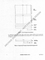
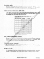
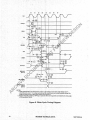
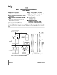
The MQ6~db offers’16 32-bit registers and a 32-bit program counter (see Figure 1),
Thetfi@eight
registers (DO-D7) are used as data registers for byte (8-bit), word (16b~$~~
~~hd long-word (32-bit). operations. The second set of seven registers (AO-A6)
~~~~r:!he user stack pointer (USP) may be used as software stack pointers and base
qj~~ddress registers. In addition, the registers can be used for word and long-word
~! ‘operations. All 16 registers may be used as index registers.
,
.
m
MOrOROLA
m
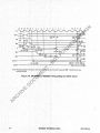
The SR (see Figure 3) contains the interrupt mask (eight levels available) as well as
the following condition codes,: extend (X), negative (N), zero (Z), overflow (V), and
carry (C). Additional status bits indicate that the processor is in a trace (T) mode and
in a supervisor (S) or user state.
‘,?...
SYSTFM
I
R~
‘ “-””’---”
6. Implied
.
Included in the register indirect addressing modes is the capability to perform postincrementing, predecrementing, offsetting, and indexing. The program counter relative mode can also be modified via indexing and offsetting.
MOTOROLA
MC68000 TECHNICAL DATA
3
: ..
i
1’ ““.
I -.+.
I
,
I
u.
I
..
. :a~,“y*~-
? . >\k,
-w
“%$,:
--
,,,..,
~u.lull
.OGL
I=
IIbL~U
~il
subsets of these instructions
I ~UI~
~.
~aal~lonal
Instructions
that
are listed in Table. 3, Special emphasis
are
is
fion set’s support ,of structured high-level languages to facilitate
‘am”ming. Each instruction; with few exceptions, operates on bytes, words,
...-1–
,
t instructions can use any of the 14 addressing modes.
nstructton types, data types, and addressing modes, over 1000 useful
vi~ed. These ‘instructions include signed and unsigned, multiply
quick arithmetic o’peratiobs, BCD’ arithmetic, and expanded operations
~s), For detailed information
on the’ MC68000 instruction
set refer to
-,—. —.
8000 Programmer’s Reference Manual.
.-
.$et ~ummary
RESET
ROL ‘
ROR
ROXL
ROXR
RTE
RTR
RTS
Reset External
Dms
Rotate Left y&.&6@~~xtend
Rotate Rigkfl@%@ut Extend
Rotate L~$~]~”Etiend
Rotate .RIg~J with Extend
~ Ret~~~~{~m Exception
,L@*~~$a nd Restore
.4+ ~$t$n from Subroutine
SBCD\$ “$~ Subtract Decimal with Extend
Scc f:+’k%,,, Set Conditional
stop
~~bm: “
Subtract
:&&$*
Q~AP
Swap Data Register Halves
~AS
TRAP
TRAPV
TST
UNLK
Test and Set Operand
Trap
Trap on Overflow
Test
[ Unlink
,.
.,.
.
.,.
,,,
..,,
,.
:.!
,,.,
,,
,’
,’,
,,
,.
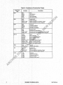
Table 3; Variations
Instruction’
Type
ADD
.,
ADD
ADDA”
ADDQ
ADDI
ADDX
‘
AND
“’
,.
\
CMP
,,
,’
,
:,
MOVE
,,
,$
Add
Add
Add
Add
Add
,
“Address
‘Quick
Immediate
with Extend
AND
ANDI,
ANDI to CCR
‘ANDI to SR
Logical AND
AND, Immediate
AND Immediate to Condition Codes
AND Immediate to Status Register
CMP
CMPA
CMPM
CMPI
Compare
“
Compare Address
Compare MemorV
Compare Immediate
.
,,
,
Exclusive
Excltisive
Exclusive
Exclusive
.,.
NEG
.$~$~; ‘3 Negate
NEG~+T~@>’~) ‘
Negate with Extend
‘.,~1’t,
.i’,
oQ,:~~~p. “
Logical OR
.QRQ,%”$*
OR Immediate
OR Immediate to Condition Codes
a<?~k$?o CCR
OR Immedia?e to Status Register
..@eF:$:
;:.,.#R1 to SR
‘
~<,$k<$,,;~
‘,i:
,
$,;
J’,:.
.,)~.
, ,.,,:
,~%::+:,.
.,!.? ,x,
,,K*,
,,>,,$..
,*p,?t
~
,~ ,&y,3
g, ,*tg?
“
*.rii,,.‘:., “
.:}>,<..... ..”
%.~,.
,, ,s:..
~~+%
6.,.
~ .$8:$?
*..,.
.*.
,k$:.$‘,<i~.,
isi
t;!
,,~~,.,,:$>
.,,.:?,i<
,\,
.<,~.~
\i$:!..~J
.$,.
,,k
,<h.);,..,
...
Q,?
.,,,.
.,,,.
.**.
<;J’+9V$”$
“t~$.!,,
~$$,
SUB
,,
.
EOR
EORI
EORI to CCR
EORI to SR
,,
OR
Description
,“
:,..,.>,
,s‘,MY,
*>,*,
OR
%~:,,
..%
OR lmmediate,&t)
-+
OR lrnmediat&~~&@ndition Codes
OR lrnme~~”~$~~&Status Register
-~ ..\<i>.F:#t\,,.\:.:.
,.~:.$?
Move
MOVE
*.,.*+*
Move Addre~;
“fit
MOVEA
MOVEM
Move Mul~~l*~~egisters
MOVEP
Move Pq~p~~ral Data
Move ~~ki~’
MO’VEQ
MOVE from SR
Mov@@fi
Status Register
MOVE to SR
Mo~e ~b Status Register
MOVE to CCR ;,$~; Move to Condition Codes
MOVE USP *$ >t.~ove User Stack Pointer
EOR
..
NEG
.Variation
of Instruction Types
SUB
SUBA
SUBI
SUBQ
SUBX
Subtract
Subtract
Subtract
Subtract
Subtract
Address
immediate
Quick
with Extend
..
,,
,.
,,
,,
,.
.
,.
,.
,.
6
,
MC68000 TECHNICAL DATA,
,,
,.
MOTOROW
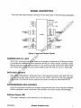
SIGNAL DESCRIPTION
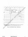
The input and output signals (see Figure 4) are described in the following paragraphs.
PERIP#L, .COWROL
_
‘-
----- ..
CONROL
1*
-?
~
—
kigure 4.1
+;
$*F ,,.*+,:.,
ADDRESS BUS (AI-A23)
~$~y
,,:.$,~+y
-2
This 23-bit, unidirectionai~~$~~-state
bus is capable of addressing 16 Mbytes of data.
It provides the addre~~’~%~@busoperation during all cycles except interrupt cycles.
During interrupt cyq~,~~,<~ddresslines Al, A2, and A3 provide information about what
level interrupt is b~n$’serviced while address lines A4–A23 are set to a logic high.
~,,.i:~’~
:(,~i,.
,.,
..i~~l
$,;:4,
*$
?’:J
...
.
.
~,:”>!*:,t,,.
‘ATA
Bu:.Jg~col
i-.J,,,;<$5)
This ~,~~~$ ‘bidirectional, three-state bus is the general-purpose data path that can
tra~sf~~dnd accept data in either word or byte length. During an interrupt acknowl.+~~$~dycle, the external
~.l~~:
,?::>
...
.,,.~]
:..,y,(~}.,
i~:$:\~
device supplies the vector number on data. lines DO–D7.
ASYNCHRONOUS BUS CONTROL
Asynchronous data transfers are handled using the following control signals: address
strobe, read/write, upper and lower data strobes, and data transfer acknowledge.
Address Strobe (AS)
This signal indicates. a valid address on the address bus.
-,
.;..,
.:
::.:
I
,
[
I
., ,..
w,,
I
I
.:
I his input in@ic&{@%
that the data transfers complete. When the processor recognizes
DTACK d~~$~~ia.read
cycle, data is latched “andthe bus cycle is terminated. When
. ...
$~$,&us request, bus grant, and’ bus grant acknowie~ge form a bus arbitration circuit to
$,,;..,
. ‘ch ‘device will bethe ‘bus master.
This input is wire’ORed with all other devices”that could be bus masters. This input
‘indicates to the processor that another device wishes to become the bus master.
:
Bus Grant (BG)
This output indicates to all other potential bus master devices that the processor
release bus control at the end of the current bus cycle.
Bus Grant Acknowledge
will
\ $,,
...
~{tv~)$:v?
,>\$\.\
~,.}.
*:.~.\&.
,
(BGACK)
This input indicates that some other device has become the bus master. Th~#~~#~al”
should not be asserted until the following four conditions are met:
.,, ~~~.~
.*.$
\&,+
.**,
:.!
,,+>
!,,*3 .\\
1. A bus grant has been received.
,.~f+
~$;,,,
~$:
~.’.’
.\:\, ... .2, Address strobe is inactive, indicating that the microprocessw
i&+#ot using the
“~~
~~:.
:?:
..\.*::F;t.
bus.
.,::,,
\
‘:J*,.
;l),},.:i
-‘Y?$~
!,
:!J:,.
.$‘ “,,
3. Data transfer acknowledge is inactive, indicating that ~~@br memory nor pe- ‘
S>:,:,.px:,,.$..k,
,.,~
ripherals are using the bus.
“?!:.*
..,\*
,.
‘,.~*.;$\
“4. Bus grant acknowledge
is inactive, indicating ~k~$~d other device is claiming
~$
$~ 3.*
bus mastership.
,s~.
*L
,+‘,i’y*,.,>
.$:;$}$,$$*.
,;$! w:
~,:}$*
$,)2
,,
—
_
INTERRUPT CONTROL (lPLO, IPLI, IPL2), R] ‘%
‘4(.$.
i(,fi,.~,e.
These inputs indicate the encoded priori$;~~el
of the device requesting an interrupt.
Level 7 is the highest priority; level O,in~icates that no interrupts are requested. Level
7 cannot be masked. The least sig~~fi$ant bit is given in IPLO, and the most significant
bit is contained in IPL2. These,,.l$@s must remain stable until the processor signals
interrupt acknowledge (FCO-~$~~?e all high) to ensure that the interrupt is recognized.
(T~+$,
‘$$
“d,’..!~~,
t~+h..l,.,..
,,.
~,~;.$k:~.
,\$:,,
J~,.)&,\,
.
SYSTEM CONTROL
f’~i]$ ‘
The three system ~$’n~~~l’inputs are used to reset or halt the processor
.~?e.
.).“*&</s*
to the process~gi,t~at bus errors have occurred.
~.,..,:~$
,,. ,,.,
,,.P
>$~
~,,,.,,..,
.,<.
,
.:,
.’*
K$:
,,\$
.\\..~.
.’
and to indicate
Bus Error.,lf&~*R)
.*S
,,\:.j*
Th~~/~~~? informs the processor that there is a problem with the cycle currently being
~;~%uted. Problems may be a resu It of:
,&,,~J~~ Nonresponding
devices
“!?>2. Interrupt vector number acquisition failure
‘“ 3. Illegal access request as determined
by a memory management
unit
4. Other application-dependent
errors
The bus error signal interacts with the halt signal to determine if the current bus cycle
should be re-executed or if exception processing should be performed.
MOTOROLA
MC68000
TECHNICAL
DATA
9
.
??*Y).
,.$:,.,,,
.,,?
he standar~:$w~le signal common to all M6800-type peripheral devices.
r this O$~$?~&~IS’1
O MC68,000 clock peri’ods (six clocks I,ow, four clocks
1. Enable ,is g~~,$[~+~d by an internal,ring counter which may come up in any
(i.e., at pow&$-ti$,
~>$ti;b
3*,,?’.it, is impossible to guarantee’ phase relationship of E to CLK).
~ free-run~~~$clock and runs regardless of the state of the:btis on the MPU.
PROCESSOR STATUS (FCO, Fcl , FC2)
These function code outputs indicate the state (user or supervisor) and the cycle type
currently being executed (see Table 5). The information indicated by the function
code outputs is valid whenever address strobe (AS) is active.
T-Ll-
,,
~v,t
.,T
E C..-A*:--
PAA- nm.+m.m+e
.>> i,.
*.\,:,,.,>; :,?
,,..
.Transfer of ~at~i$&tween devices involves the following
1. Addr@~4~us Al -A23
2. Daf@&’s DO-D I 5
signals:
3,:c!$**~ol signals
T~~*~Mress and data buses are separate parallel buses used to transfer data using
,4~~~~@5ynchronousbus structure. In all cycles, the bus master assumes responsibility
.*...’%r
deskewing all signals it issues at both the start and end of a cycle. In addition,
?J‘.(yj,!>>>
‘~. the bus master is responsible for deskewing the acknowledge and data’ signals from
the slave device.
The following paragraphs explain the read, write, and read-modify-write cycles. The
indivisible read-modify-write cycle is the method used by the MC68000 for interlocked
:ycle, the processor receives data “from either memory or a peripheral
device, Thep,rocessor reads bytes .of data in all cases. If the instruction specifiesa
word (or double word) operation, the processor reads both upper and lower bytes
‘simultaneously by asserting both upper and lower data strobes. When the instruction
specifies b~e ‘operation, the processor uses an internal AO bit to determine whiq~
byte to read and thenissues t he data strobe required for that byte. For byte operaQ,@~$$
when AO equals zero, the upper data strobe is issued. when An enllal~ rine tha#n&~k’~r
~
cessor sends data to either the @@@ory or a peripheral
,,.~,?.\,:*?ii
‘~,ti’
device. The processor writes bytes of data in all cases. If th~~thstruction specifies a
word “operation, the processor” writes both bytes. Wh@@$Qe instruction specifies a
..
I-. .Lthe, processor uses an internal AObit ~~v~~termine which byte to write
; the data strobe required for that h~$~’~or byte operations, when AO
GqU~iS
zero, ~ne upper data strobe is issued: ,~iheti AO equals one, the lower data
..
-+.-ka :A’:--. .-J
....
The exception processing state is associated with interrupts, trap instructions, tracing,
and other exception conditions. The exception may be internally generated by an
instruction or by an unusual condition arising during the execution of an instruction.
Externally, exception processing can be forced by an interrupt, a bus error, or a reset.
.Exception processing is designed to provide an efficient context switch so thatt~~
,k:;~p
~J:
,
processor may handle unusual conditions.
,$?:.~?’
,:,
~
’ii.
,~!.
~:,,,>>,1>>~,
,.’~,
.?\,,,
~.s~,,w,,k$
,*+*!,~.,~t.
:f,.J.)>
#+$,
\*\\...
,,:
.,~.,..
~j.
~,.:$.,,,>
4.\:l\
s-..
,,~.
.*,:*
,,,;.s
,,,,j~,,.,~~
,
~$$..<,4
HALTED PROCESSING
The halted processing state is an indication of catastrophic har~~&~##ailure.
For
example, if, during the exception processing of a bus error, anoth&~&:userror occurs,
the processor assumes that the system is unusable and haltsti~,~~an
external reset
can restart a halted processor. ,Note that a processor in the$~~t&@pedstate
is not in
;~j~.,t,,
,t<y:),$,,
.s,. ..
the halted state, nor vice versa.
~.:
,,:.*.‘~,.:i,,
.
,.;f.>.>
,..’,”.:l~k$p
~>tl,~i!i:,$at,
..J:
,,.
iNTERiAcE WITH M6800‘Q#kfPHERALs
,i”+-~
J
~
,:
.!,.::\*,,.
Motorola’s extensive line of M6800 perip~#~~l$ are directly compatible with the
MC68000. Some devices that are paflicu~~~}~&seful are as follows:
MC6821
Peripheral Interface Adapter’’k’*”*
MC6840
Programmable Timer ~dflle
~~)~~.
‘*Jt.,,,,.
,
MC6845
CRT Controller
\wa,~
,,::\~.!:.,
>:J:>,.
MC6850 Asynchronous C~Q,&~nications Interface Adapter
MC6854 Advanced Data ~~fik$~ontroller
<$:,:++:~q”.$\,.
To interface the synchroq~#~6800
peripherals with the asynchronous MC68000,
the processor modifie,~~~$us cycle to meet the M6800 cycle requirements whenever
an M6800 device ~~~,~$% is detected. This modification is possible since both processors use me,~<$$~~~apped 1/0.
.<.\”i:
,. :f
,..~
... ‘~.~$>
,~,
,&
~,f$”~
,:~.}
.,$,,.
.“‘+*S*
‘:}*,
‘v~.k,..$
,.+
,***%
.. ,.,~
*J
!.$*tj$
~x<~q,,
..$$*.
.,..~,,>$..<,,~
.,.,
MOTOROLA
MC68000, TECHNICAL DATA
13
,..
.:
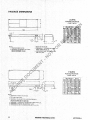
Ilue
,v~~
I
~..
– U.o 10:
+7.0
ckage l~etmal
-$
,.,.
.“<+*.
~ v“
-o.3’to +7.0
o TM
1’
Unit
I -40t085
Resistance,
v
‘c
‘
!
The device contains protection
circuitry against damage due to
high static voltages’ or electric
fields; however, it is advised that , ‘$~t,
normalprecautions
betakent~ ~~&~
.l.$.,*I.
avoid application. of voltag~s ::+.U
higher than maximum-rated%k,+sv-
cuit: Reliability
of.o~~$~~&#
is
enhanced if unused JnwYs se tied
Junction-to-Ambient,
‘Cm
e K is a constant. pertaining to the particular part. K can be determined from
tquation
(3) by measuring PD (at thermal equilibrium)
for a known TA. Using this
‘ ! of ’K, the values of pD, and TJcan be obtained by solving Equations (1) and (2)
.,-
.’
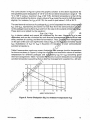
The curve shown in Figure 5 gives the graphic solution to the above equations for
the specified power dissipation of 1.5 W over the ambient temperature range of – 55
‘C to 125 ‘C using a maximum 9JA of 45 ‘Cm. Ambient temperature is that of the
still air surrounding the device. Lower values of OJAcausethe curveto shift downward
slightly; for instance, for 6JA of 40 ‘~, the curve is just below 1.4 W at 25 ‘C.
,.’”
:~:..:
\
The total thermal resistance ofa package (6JA) can be separated into two compo:Q@&
6JC and OCA, representing the barrier to heat flow from the semiconductor iu~d~e’n
‘:,y,i
‘,j’\>,
~.,?:.
to the package (case) surface (6Jc) and from the case to the outside ambi:~~~$@CA)l
,,,~,,,
., “~
s:i
~“
These terms are related by the equation:
,$,,
,$*
,,,*, ~:...d
\.\
,
.<,.
~J’
“~w~,.
t,~
8JA=6JC+OCA
(4)
“i:.}j:*y
6JC is device related and cannot be influenced by the user. How~veF#OCA is user
dependent and can be minimized by such thermal manageme~$~&&niques
as heat
sinks, ambient air cooling, and thermal convection, Thus, goqi$~~~$$~al management
on the part of the user can significantly reduce 6CA so that ~~$$,~~proximately equals
O.In. Substitution of O Ir for 9 1A in Eauation (1) resultw~n’:% lower semiconductor
temperature.
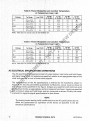
Table 6 summarizes maximum power dissipatik~ #kd average iunction temperature
for the curve drawn in Figure 5, using the mi~i~~
and maximum values of ambient
temperature for different packages and s~~piuting
9JC for OJA (assuming good
thermal management). Table 7 provides t%~aximum
power dissipation and average
junction temperature assuming that no t~ermal management is applied (i.e., still air).
,.*:$i;
>’”C2..
I
Figure 5. PowerDissipation
I
(PD) vs Ambient Temperature
(TA)
,,
,,
,
Package
TA Range.
O“cto 70°c
– 40°Cto 85°C
ULC
I
6JA PCW)’
’15
15.’.
,
I
,,,.,’,
I
‘“~p:A\;~”
TJ (“C)
@ TA Min.
1.5
1.7
22:5
–14.5
,
.
1
PD (W)
@ TA Max.
TJ (°C)
@ TA Max.
‘1.2
1.2
I
..—
88
103
I
,,
.,
\
-----
,:.%
, ..~,
L\y.i,
‘ ,i ,l
~,,+,,,
.
:TRICAL SPE$*TIONS
..,e..,.’$$,..,
iy
DEFINITIONS
\C specificati&WSk~tesented consist of output deljays, input setup and hold times,
~.,%
%},.”
.*?
;ignal ske&l~~;&s.-All
signals are specified relative to anapp,ropriate
edge of the
..,,”6.
... ....!+
.
.
2.0 v
!!,
ti$,\
Load Capacitance
1~1
.. . \
,’?
HALT
All Others
s:s~>.t,$~”
,,$.
.*$*, ‘,*k
I,*
.?.? ,,1
CL
—
—
70
130
pF
.,1
*With
exterd’~<til~up
resistor
of 1.1 KQ.
AC E~~@~RICAL SPECIFICATIONS — CLOCK INPUT (seeFigure
,<..,,
..? ,.>.
>.~~
I
1
Clock Pulse Width (Measured
I
4,5
from 1.5 V to 1.5 V for 12F)
I
Clock Rise and Fall Times
I
tcvc
Cycle Time’
2,3
I
I
tCL
tru
-v!
4
tcr
tcf
*These specifications represent an improvement
over previously published
and are valid only for product bearing date codes of 8827 and later.
I
125
250
55 125
1 5511251
—.
—
100
I
45 125
4511251
10 “—
10 —
specifications
250
10
10
7}
I
l..
.. .
I
1
:
35
125
35 11251
27 62.5
ns
27 162.51
—
—
—
—
5
5
5
5
ns
for the 8-, 10-, and 12.5-MHz MC68000
I
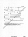
AC ELECTRICAL SPECIFICATIONS (VCC=5.O
Vdc*5Yo;
GND=O
Vdc;
TA=TLto
TH;
READ AND WRITE CYCLES
see Figures
8 and 9)
8 MHz*
Num,
Characteristic
10 MHz*
Clock Low to Address
6A
Clock High to FC Valid
7
Clock High to Address,
Valid
tCLAV
—
62
—
50
—
tCHFCV
—
62
—
50
—
tCHADz
—
80
—
70
—
tCHAFl
o
—
‘o
—
o
Clock High to AS, DS Asserted
tCHSL
3
60
3
so
3,
Address Valid to ~, ~ Asserted (Read)l~
Asserted (Write)
——
FC Valid to AS, DS Asserted ‘(Read)/~
Assefled
——
Clock Low to AS, DS Negated
tAVSL
30
—
20
—
Data Bus High Impedance
16.67 MHz
’127
Unit
Min Max Min Max Min
Min Max
6
12.5 MHz*
Symbol
50
—
60
—
Max
50
ns
—
ns
(Maximum)
8
gl
112
IIA2
121
132
Clock High to Address,
——
AS, DS Negated to Address,
142
~
(and
~
14A
~
Width
152
~,
~
Asserted
Width
Clock High to R/~ High (Read)
212
Bus High Impedance
Negated to R/~ Invalid
Clock High to R/~ Low (Write)
Asserted
Address
to R/~ Valid (Write)
Valid to RI~ Low (Write)
21A2
FC Valid to R~
222
R/~ Low to ~
23
Clock Low to Data-Out Valid (
——
AS, DS Negated to Data-Qu
252
Low (Write)
Asserted
(Write)
262
Data-Out Valid to ~
275
Data-In Valid to C!@%,#&w?Setup
282
29’
,,,,
,.,.
,..}$!:~.>
....
.;*,.,. .,$.
i~*,$.\.,;$:~,\\
*
$~+p$ ,>
&#ef&fWrite)
70
.k$~ ‘:~~
—
30
—
ns
tCLSH
—
62
.*:
;$bo~ $—
40
—
40
ns
tSHAF\
40
–,3$ ,:~~;~t
14
tA\/Rl
-“, ,-.
—
—
70
—
60
—
50
ns
—
30
–
20
—
10
–
ns
55
0
45
0
40
0
40
ns
55
.-
0
45
0
40
0
40
ns
10
—
10
—
10
—
10
ns
1 20 1 — I o
—
o
—
o
—
ns
—
50
—
30
—
20
—
ns
tR LSL
80
—
50
—
30
—
20
—
ns
tCLDO
—
62
—
50
—
50
—
50
ns
tSHDOl
40
—
30
—
20
—
15
—
ns
—
20
—
I
40
.-
—
1
.. ,
O ]240[”0
11
190
0
150
0
110
ns
tSHDll
o
tcun7
-“, ,“L
—
—
—
o
—
o
—
ns
187
o
I
150
---
—
120
—
go
ns
—
“o
—
o
—
50
—
0
200
o
[
—
—lolI
1
1
—[65
200
0
200
I
—
I
ns
40
ns
0
150
ns
40
ns
trucl
—
62
—
50
—
40
—
62
—
50
—
40
—
40
ns
tBRLGL
3.5
1.5
3.5
1.5
3.5
Clks
Negated
tBRHGH
1.5
3.5
1.5
3.5
1.5
3.5
1.5
3.5
Clks
tGALG H
1.5
3.5
1.5
3.5
1.5
3.5
1.5
3.5
Clks
1.5
Clks
ns
to ~
Negated
BGACK Asserted
to ~
Negated
Asserted to Control, Address,
Impedance (~ Negated)
Negated
ns
1.5
BGACK Asserted
Width
ns
—
3.5
37
1~
—
7
1.5
37Aa
39
15
10 —
I
tCHGH
~
~
?n
-.
Asserted
367
38
t
1 lol 1 —llolI .- 1 —
Data Bus High
~
1
-., .
,
—
Negated
Negated to =
ns
ns
—
tRHrf
to ~
—
—
65
and RESET Input Transition
Clock High to ~
60
ns
—
c31 1
% Asserted
—
—
105
—/901
‘$:? ‘?’ 34
,*,!
35
80
120
80
tnAl
-, .--,nl
Asserted
—
—
tSH~EH
Clock Hiah to ~
160
60
Data-in High Impedance
=b,${$~$$ted
.
30
~~~egated
to BERR Negated
,,’, .,.‘!,..
31 ~.sf +*
Asserted to Data-In valid (Setuo Time)
‘3Y
–
60
tsHnAH
-. .-,
~me
1101–lnsl
20
tFCVRL
tDiCL
to
“t%5’1 —
270 .:**
tDOSL
Time on Read)
~ Negat@$$’Q*
Negated
(Asynchro#$~s ‘@old)
.
.i,~.+
~, ~,~~ted
to Data-In Invalid (Hold Time on Read)
29A
—
.,.
8+$*NJ
tS H ~+$>
.:?,
,>~a,~y’
tc~z
f$i~, —
,,.:{$,,,,
40
. .EHRH
,..:,: .,q,l
$..:/:.5 t@RH
o
..,.......
‘~J:<.
~:$:$is..:t;
~$~~ URI
o
tctll ,G
“${$
,,:>
tASRV
—
G,
t.-
90
tSL
Negated
181
~
tFCVSL
tncl
-“ .
~,
20A2,6
(Write)
(Write)
172
1Q: ‘~~: @15
..
.
‘~~:.,,:P
. ,.,.
t,:.
Read) Width Asserted
Clock High to Control
~
(Minimum)
FC Invalid
16
203
I
#
FC Invalid
——
tGALBRH
20
1.5
Clks
20
1.5
Clks
20
1.5
Clks
10
tGLz
—
80
—
70
—
60
—
50
ns
-SH
1.5
—
1.5
—
1.5
—
1.5
—
Clks
1
ed to .E High
I
1
lnuul
GDa
1 :Ulu
“
:
tcLvM~
I
tVMLEH
,
I
I
I
1.5
,—
I
.,.7?
-+*,
,-,1.51$J
“.*!J\\ ~~
I
I
I
. ,.
‘“
tE~
564
R~ Asserted to Data Bus lrnpedanct
—_
HALT/RESET Pulse Width
,57,
-— .,
5/A
Negatedto’~,
~, Rfi Driv
1BtiACK Negated to FC, ‘VMA Driven
Zn
., ,.:?$+
.: !., t~RpW
.,,,. >,.}.
,~y
,.<$,
,“$’~q~+,,
—
45Q! ~+
’550
..>.. .>..
,,
,.’,
11501-
I
1.5
I
~~ tSHEL
,,.
:55
70]—17
I
tBELDAL
——
S, DS, Negated to E Low
,,
,
I
tGAL
?d
-
]2001–
1
1 Illlc/
th’Low
Mdth’ High
!
10
I
—
tGAFD
1
tRHSD
1.5
—
10
I
I
10
I
1
I
1.5
—
1.0
—
–
1.5
—
Clks
I
—11[—l
—11
—
280
I
1 I –
Cl ks
lClksl
-
~~.;t~i
: improve~~$:~y~r
&
previously ~ublished specifications for the 8-, 10-, and 12.5-MHz MC68000
——
and BERR, #48 may be ignored. In the absence of DTACK, BERR is an asynchronous
.—.
)0 must be held in the’reset-state for 100 ms to allow stabilization ofon-chip circuitry. After the
....,. .:x
rw u$, #56 refers to the minimum pulse width required to reset the processor.
*J**.
_
asyn@:?~nou3 Input setup time (#47) requirement is satisfied for DTACK, the DTACKJ”asserted to data setup time
req~~P@3$?@t
can be ignoredl The data must only satisfy the data-in to clock low setup time (#27) for’the following
.,
,,
w&r&. ‘?
d (*20Y.), subtract 5 ns from the values given in these columns.
arhitra?jon
logic
neaates
~
before
asse~ina
eain drivina the bus aaain if external
-
-.1-
,.--,
“,,
n occur first, depending, upon the loading on each signal. Specification
.
“–u
.-—
--------
#49 indicates the absolute maximum
Ie rising edge of the strobes and the falling edge of E.
,,
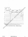
AC ELECTRICALSPECIFICATlONS — PERIPHERAL CYCLES TO M6800
(VCC=5.O Vdc*5%;
GND=OVdc;
TA=TL
to TH; see Rgures
10 and 11)
1
I ‘urnI
Characteristic
I
I ‘Ymbo’~
I
——
Clock Low to AS, DS Neaated
121
,
trl
r
1
1
. .. . .... .
27
29
Data-In Valid to Clock Low (Setup Time of. Read)
——
AS, DS Negated to Data-In Invalid (Hold fime on Read)
40
Clock Low to VMA Asserted
I
1
,
r
I
I
1
1
,.
,
,
X*:T
,.,.
I
1
-bLul
t~,~,
llnl_llrrl–
tSHpll
Inl–lnl
trl
?n I –P?.
_
n .l**C~*<K
I –
-
, ,“
, “
, 4“
,,s
In
_
I In
—
~e
!1
I
I
——
44
AS, DS Negated to VPA Negated
45
1 -u, ,”,,,
E Low to Control, Address Bus Invalid
t~l
rAl
,
I
-
,,.s.-s, ...-., .,>,,
, --
10
—
~i~~”
..
I
,
,
“
I
—
1
.= r
... ,.,
,
,
1
r
1
I
I
.,
,.
7.
Clock High to Address,
(Maximlum)
16
Clock High to ControlBusHigh
33
Clock Highto
34
Clock High to ~
Negated
35
~
37
,.
37A2,
38
~’Negated
to ~
BGACK Asserted
10 MHz*
12.5 MHz*
Min
Max
Min
Max
Min
Max
Min
Max
tCHADz’
—
80
—
70
—
60
—,
5~
Impedance
tCHCz
—
80
—
70
—
60
—
tCHGL
—
62
,—
50
—,
40
.,
Asserted
—
40.
Negated
62
tCHGH
“—
—
50
tB~LGL
1.5
,3.5
1.5
3,5
tBRHGH
1.5
3.5
1.5
to ~
Negated
tGALGH
1.5
3.5
1.5
BGACK Asse~ed ,to ~
Negated
tGALBRH
20
1.5
Clkc
20
~
Assefled
,,,
to Control~,Address,
,,
= .,
,
“s
Data ‘Bus High
;
tG L.Z
,—
an improvement’ove
rQrev**i]slv
nl!hlishsd
sn~cificatinnc
NOTE: Setup time to the clock (#47), for ,tie asynchronous inputs -R,
-, -.,.
“, ,a.a”+nn- *hA;. .--- ”-:.:-,- -* .L - _- ... ‘-,,: -- -J -- -.-–
-K,
3.* ‘~g. ?3.5
%
3.5
3,5 ‘1.5,, .\t%@!*X5
,.,’.
.
.
1.5
3.5
3.5 ~$.5 ‘~di
...
1.5
10
I,?q: $*
1.5
,“
I
,,”
—
I
I
I
I
I
I
fnrthp
~R, =K,
rlbc
;&
80 l,a,~;~~~’l
I
“’*J!:,
+>*,+ ,,
_
*$$
.,,..!
.,.\,. ...+.
. *.L
+> ‘** ‘“’k ns
50
~“:
R-
C]ks
1.5
‘@ltia
I
S reDreSent
16.67 MHz
’12P
Unit
C.’—LDI
Oyllluu
.
‘Asserted
“Asserted to ~
,-
Data Bus High Impedance
~
361
8 MHz*
Ph-.-m:e+:e+:“m,
a, ati.c,
,a,, b
U,,,.
i
,.”
I
Clks
ns
rlbc
60
,“
Clks
-
I
I
~
,“
, .-
,,a
–—
1
,—,
I
—
“,ma
4
I
Q,fia
I
in-
and
~2-1=0,
19 6-NAUY
hfir~nnno
and WA
1-
v
-1,
m
CLK
(52-pin vemi~on
,..\.
n ... – .,
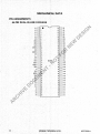
68-TERMINAL PIN GRID ARRAY
.
\
K
n.nnnnnnn
00
3
Ilnnnnn
I -’IW’’IY”
nnnnn
“:w
b
NC
i
II
II
1
I
L
-c-
PIN Al
1 DIMENSIONS
❑
A ANO B ARE
IS OATUM SURFACE.
2, POSITIONAL TOLERANCE
(68 PLACES}:
. ., ----
FOR LEAOS
4, cpiITum
IIhIC
nindchlctnht
WITH STAN~nF$
12345678910
FN SUFFIX
QUAD PACK
CASE 779-01
II U. . . . ..uul.-uu..l..
1. DIMENSIONS R AND U DO NOT iNCLUDE MOLD
MOTOROU
t +
.,
..
,L
“1,,,.,
.u,
”,.
,,,
u
“,,
Yld 5M l~R7
MC68000 TECHNICAL
DATA
33
~
.—
~’~”
“’%
:,$::<,:i
!Jolorola reserO&#@r@t
to make charges without further notice tc any products herein to improve reliability, function or design. Motorola toes not assume
any liability @*%tn&@t of the application or use of any product orclrcuit described herein: neltherdoes [t convey any hcense under its patent rights nor !he rights
of others&+$$lorQa products are not designed, !ntended. or authorized for use as components in systems intended for surgical implant Into the body, or other
aPPli~@*~s*g~ded
to suppoff or sustain I!fe, or for any other application in which the failure 01the Motorola product could create a situation where personal
inJur~~J_W
may occur. St?ould BOyer purchase or use Motorola products for any such unintended or unauthorized applica?lon, Buyer shall indemnify and
h*&loW&olaand
its officers, employees. subsidiaries, affihates, anddistribu?ors harmless against all claims, costs, damages, and expenses, and reasonable
at%@++Nees arising out of, u;rectly or indirectly, any claim of personal injury or death associated with such unintended or unauthorized use. even if such Clalm
a!le;$s that Motoroia was neg!:gent regarding the design or manufacture of ?he part. Motorola and ($) are registered trademarks Of MOtOrO!a.lnC. Motorola,
Inc. is an Equal Opportunity,’Aff irmatwe Action Employer.
Literature
USA:
Distribution
Motorola
EUROPE:
JAPAN:
Motorola
Nippon
ASIA-PACIFIC:
Centers:
Literature
Distribution;
Ltd.; European
Motorola
Motorola
Ltd.; 4-32-1,
(n
Box 20912;
Center;
Phoenix,
88 Tanners
Nishi-f30tanda,
Semiconductors
Tai Po, N. T., Hong
-M
P.0.
Literature
m,mm
m
USA
,,90
,lmEi,Al
H.K. Ltd.; Silicon
Kong.
LIm!u
,,,>4,
m,cw
HJu
Drive,
Shinagawa-ku,
MOTOROLA
.,775+3
Arizona
Y,”*
Harbour
85036.
Blakelands,
Tokyo
Center,
Milton
Keynesr
MK14
5BP, England.
141 Japan.
No. 2 Dai King Street,
Tai Po Industrial
Estate,