1
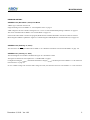
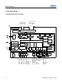
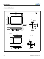
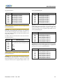
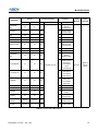
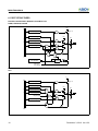
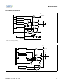
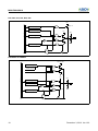
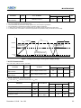
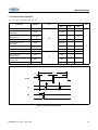
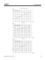
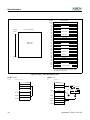
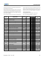
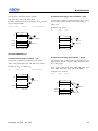
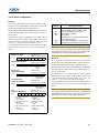
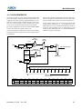
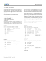
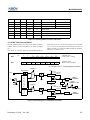
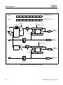
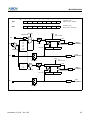
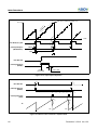
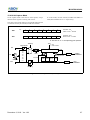
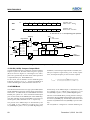
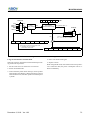
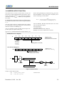
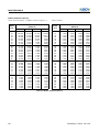
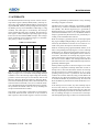
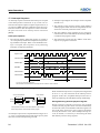
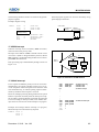
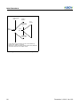
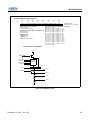
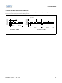
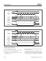
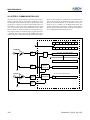
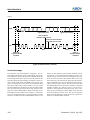
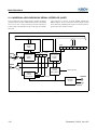
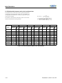
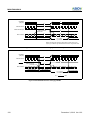
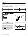
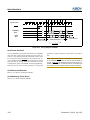
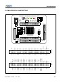
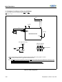
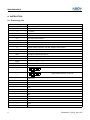
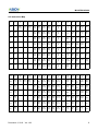
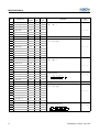
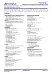
MC81F8816/8616
7.7 Serial I/O Characteristics
(TA= -40~85°C, VDD=5.0V±10%, VSS=0V)
Parameter
Symbol
Specifications
Pins
Min.
Typ.
Max.
Input Clock Pulse Period
tSCYC
2tSYS+200
-
-
Input Clock “H” or “L”
Pulse Width
tSCKW
tSYS+70
-
-
tFSCK,tRSCK
-
-
30
4tSYS
-
16tSYS
Input Clock Pulse
Transition Time
SCK
Ouput Clock Cycle Time
tSCYC
Output Clock “H” or “L”
Pulse Width
tSCKW
2tSYS-30
-
-
tFSCK,tRSCK
-
-
30
tDS
-
-
100
tFSIN, tRSIN
-
-
30
Input Setup Time
(External SCK)
tESUS
100
-
-
Input Setup Time
(Internal SCK)
tISUS
200
-
-
Input Hold Time
tHS
tSYS+70
-
-
Output Clock Transition Time
Output Clock Delay Time
Input Pulse Transition Time
Unit
ns
SI
tFSCK
SCLK
tSCYC
tRSCK
tSCKW
0.8VDD
0.2VDD
tSUS
tHS
0.8VDD
0.2VDD
SI
tDS
SO
tSCKW
tFSIN
tRSIN
0.8VDD
0.2VDD
Figure 7-3 Serial I/O Timing Chart
December 3, 2012 Ver 1.03
27