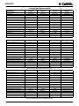
1
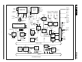
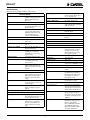
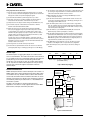
Last Time Buy Notice – Board Products
November 7, 2003
Effective immediately, DATEL, Inc. will be phasing out its line of board-level data acquisition
products. We will accept last time buy orders until February 28, 2004. Final shipments must
be accepted by June 31, 2004. In addition, all repairs and technical support must be concluded
by September 30, 2004. Please contact DATEL Sales as soon as practical to schedule your
order.
If this Notice is received by Purchasing, Materiel or Procurement personnel, we strongly
encourage you to forward this to your Engineering, Administrative and Program colleagues as
soon as practical.
Models to be Discontinued - Essentially all DATEL board-level data acquisition products, all
board-level accessories and all board software are covered in this Notice. This includes:
All ST-xxx model numbers (Multibus I boards, example ST-711)
All PC-xxx model numbers (ISA bus boards, example PC-414)
All DVME-xxx model numbers (VME bus boards, example DVME-628)
All CPCI-xxx model numbers (Compact PCI bus boards, example CPCI-511)
All PCI-xxx model numbers (PCI bus boards, example PCI-416)
Please note that many older ST-xxx, DVME-xxx and PC-xxx boards are already on very
limited availability due to component obsolescence and other manufacturing issues.
Last Time Orders - Customers should contact the DATEL Sales Dept. (Mansfield, MA, USA)
directly to place orders and negotiate delivery schedules. Some products may require minimum
order quantities and/or extended delivery. This varies over time so it is difficult to give an exact
list of such products.
To assure supply, we encourage customers to accept deliveries as soon as practical. As
time passes, customers risk non-availability of an increasing number of products. After the
customer accepts final order acknowledgement, all orders placed will be firm and noncancellable.
Warranty - DATEL’s standard warranty terms apply except the warranty period. As the date
of last shipments approach, warranty support and repairs will terminate on September 30,
2004. Customers must immediately perform a functional inspection on any shipments near this
date. DATEL will have no technical or repair facilities after this date.
Technical Support - Since some DATEL engineering resources have already been reallocated,
support and repairs are currently limited and more will be withdrawn over time. We encourage
users to get all support issues settled as soon as practical.
Replacement Products - DATEL is not aware of any competitive manufactured products which
are exact replacements for these products. However, there are numerous items with similar
functions. These will require re-integration with your application.
Manufacturing Rights - DATEL is not offering manufacturing rights on these products. The
difficulty here is the complexity of technical support to fully transfer all comprehensive details of
manufacturing (including test fixturing, component specifications and device programming). Most
of these products would require considerable re-engineering by the user to resume production
outside DATEL. Nor will we retain spare parts after September 30, 2004. Volume users
should contact DATEL to discuss their needs.
*******
As very large volume component users ourselves who are subject to frequent component
obsolescence issues, DATEL sincerely regrets any inconvenience this Notice may cause our
customers.
11 Cabot Blvd, Mansfield, MA, 02048 USA, website: www.datel.com
Phone: 508-339-3000 FAX: 508-339-6356 E-mail: [email protected]
PCI-417 Series
®
®
INNOVATION and EXCELLENCE
Advanced Performance Analog Boards
For Desktop PCI Bus Computers
FEATURES
• Simultaneous A/D sampling with no skew delays
• Collects gigabytes of non-stop A/D samples
• Analog input options up to 40 MHz
• Up to 512 Kb on-board FIFO A/D memory
• For radar, DSP, FFT and signal processing
• PCI bus master DMA burst block transfers
• Two simultaneous streaming D/A waveform outputs
• Windows® 98/NT/ME/2K/XP device driver, DLL
Visual C++ software and ActiveX controls
• Rich program library source code for developers
In a departure from standard A/D system architectures, the
PCI-417 family is a high performance fully streaming A/D-D/A
board series with advanced multichannel 32-bit ADW analog input
modules and up to half a megabyte of FIFO (first-in, first-out)
on-board A/D sample memory. The wideband analog options cover
12 to 16-bit A/D resolution, one to 32 simultaneous channels and
up to 40 MHz A/D sampling. Both the carrier board and the analog
section uitlize very high density programmable logic for efficient
integration with the PCI bus. The entire system is intended for
continuous, non-stop rapid acquisition of analog waveforms to host
memory, network link or disk array.
By properly using the on-board PCI bus master DMA controller,
the PCI-417 will collect hundreds of megabytes of high speed A/D
data to host memory without sample loss. Using a fast host disk
(especially a RAID system) will collect many gigabytes of data.
The PCI-417 is ideal as a wideband “front end” for Digital Signal
Processing, FFT (Fast Fourier Transform) and advanced signal
analysis applications of all kinds.
Modular 32-bit Pluggable Analog Module
The A/D section is contained in a pluggable ADW series analog
module. With some limitations, any PCI-417 may be converted
to another version simply by swapping ADW modules. The ADW
architecture features a full 32-bit wide bidirectional local interface to
the on-board FIFO memory and PCI bus interface. Each A/D option
includes separate A/D converters for each channel and a very
efficient method of combining multiple channels into long frames
of data.
A/D clocking may use an on-board programmable Frequency
Synthesizer (up to 40 MHz), local crystal oscillator with
programmable binary divider, external user-supplied clocking or
from a custom-frequency on-board oscillator module. Frame
triggering is either from an internal crystal-stabilized timer or from
external analog or digital triggering. The analog trigger uses a
threshold comparator formed from D/A channel 0.
Each frame is selected by an on-board 24-bit (16 million sample)
programmable Sample Counter which terminates the frame when
the sample count is reached. Triggering may occur once per
frame (with automatic sample count reload) or may run indefinitely
(“forever”) to collect unbroken data streams of any size. A special
pretriggering mode collects data before and after an external
trigger starts the sample count down.
Streaming Analog Outputs
Two 16-bit D/A channels are included in the output section
which is fully streaming by virtue of an on-board FIFO memory
dedicated solely to the D/A’s. The PCI-417 emphasizes high speed
simultaneous multi-channel sampling and low system noise for
waveform I/O applications. The D/A converters sample together in
parallel, using the upper and lower halves of a 32-bit word. Each
D/A is fed by a 8192 sample FIFO memory (4Kx32) so that
the host CPU does not require constant servicing of the output
section. The D/A’s may be programmed directly (FIFO is bypassed)
if preferred. Each D/A features both 50-Ohm current and voltage
outputs.
For discrete I/O and external device control, a programmable 24-bit
buffered digital parallel I/O port is included with the data direction
selectable in bytes. A spare programmable 16-bit timer with 10
MHz crystal timebase is also available for any purpose and may be
configured as a D/A FIFO sample clock.
Software
Each board is supplied with a Windows software system which sets
up the board, starts A/D or D/A sampling, saves data to memory
or disk and displays signal waveforms. This software is available
in source code as a comprehensive programming example.
The PCI-417 is offered with an optional full Visual “C++” DLL
programmer’s library (model PC-CDROMS) for Windows 98SE, NT,
ME, XP and Windows 2000. Multiple boards may be operated
simultaneously in one computer.
The PCI-417 family includes detailed register-level documentation
for full support of programmers. The product is furnished on
a single long PCI-bus board which is compatible with desktop
computers.
DATEL is a DATEL, Inc. trademark. LabVIEW is a National Instruments
trademark. Pentium is an Intel Corp. trademark.
Windows, ActiveX and MS-DOS are Microsoft Corp trademarks. StarDAS is a
Hyperception trademark.
DATEL, Inc., Mansfield, MA 02048 (USA) • Tel: (508)339-3000, (800)233-2765 Fax: (508)339-6356 • Email: [email protected] • Internet: www.datel.com
®
WRFF
Analog
Inputs
Reset
Synchronous
FIFO A/D
Memory
32
Pluggable ADW
A/D Module Family
Half Full
Clock
AWG
4
SSH
ADW Control
Bus
Type
A/D Channel
Address
U19
C
Clock Select Multiplexer
1
2
3,7
10 20 40
MHz
÷2
÷2
Freq.
Synth.
A/D
Clock
32
1
Internal
Trigger
32
SG15
SG16
40 MHz
External
A/D
Clock In
J6
50Ω
Internal Trigger
C
Registers
& Control
SG1
Xcvr
EOS
Clk1
PLL Code
14
20-40 MHz
10 MHz
D/A FIFO
Memory
24
0
SG2
DAC 0
External
Trigger In
P5-30
50Ω
CLKAWG
16
SG11
15-0
A/D
Trigger
Select
A/D
Sample
Counter
16-bit
Divider
External
D/A
Clock In
J5, P5-4
31-16
A
External
Clock
SG13
DAC 1
DAC 0
Vout
B
4
D/A
Clock
Control
Marker*
In
P5-14
Channel 0
J4
J3
External
Digital
Trigger
External
Analog
Trigger In
2
40
MHz
External
WR
PTDAT
5
User
OSC
5
ADW
Control(3)
8
Channel 1
J1
J2
®
P7
External
A/D
Clock In
20-40 MHz
D/A Direct and Buffered Outputs
Empty
External
Trigger In*
0 6
Analog
Trigger In
P5-12
Full
Clk2
Timer
82C54
P5
24-bit
Digital
Input/
Output
Digital
I/O
82C55
32
LED
Lamp
32-bit Local Bus
Filters
Boot
Strap
NVRAM
PCI Bus
Controller
S5933
Interrupt
A/D
Pass-Thru
State
Machine
Local DC Power
–15V
+15V
+12V
P2
–12V
+5V
±15 V
DC/DC
Converter
M1
(Optional)
Grounds
PCI-417 Block Diagram
PCI-417
PCI Bus
®
PCI-417
SPECIFICATIONS
(Typical at +25°C, dynamic conditions, unless noted)
Analog Trigger Hysteresis
ANALOG INPUTS
Pluggable Analog Input Module
The trigger will not retrigger until the
reference signal has retraced ~50 mV
from its initial trigger slope
Compatible with all current 32-bit
“ADW” series analog modules. See
the Analog Input Characteristics
tables below.
Number of D/A Channels
Two channels, 16-bit resolution
Channel Addressing <Note 13>
5-bit address code, non-incrementing
D/A Data Access
Data Transfer
Two samples (32 bits) are always
transferred with each sample clock to
the A/D FIFO memory
The 2 D/A’s are programmed in a
single 32-bit wide register so that they
update simultaneously
D/A Voltage Output Range
±2.5V @ 5 mA max
Data Format
Each 32-bit transfer sends either two
sequential single channel samples
(ADW-12M in single channel mode)
or two simultaneous adjacent
channels (all other ADW modules)
Voltage Output Settling Time
1 µSec max, full scale, –3 dB
bandwidth <Note 6>
D/A Voltage Output Coding
Offset binary bipolar
D/A Direct Current Outputs
1000 ohms, 20 mA max, 0 to –1 V
<Note 14>
ANALOG OUTPUTS
ADW to FIFO Transfer Rate
40 MHz x 32 bits min <Note 5>
A/D Module Identification
A 4-bit code identifies the installed
analog module
Current Output Settling Time
100 nS <Note 4>
D/A Current Output Coding
Inverted straight binary unipolar
On-board A/D FIFO Memory
Up to 256K samples (128K x 32)
<Note 3>
On-board D/A FIFO Memory
8192 samples (4K x 36) <Note 4>
PCI Bus Access to D/A FIFO
By I/O register transfer only
PCI Bus Access to A/D FIFO
Either by PCI Bus Master DMA or by
I/O register block transfer
D/A Clock Sources
A/D Clock Sources
On-board 40 MHz crystal divider,
on-board frequency synthesizer,
external A/D clock or user-installed
on-board oscillator
Selectable from the A/D clock or
external. The external clock may be
connected to the on-board spare
82C54 rate generator by jumpering
across a header connector.
A/D Timebase Divider
Programmable 16-bit binary divider
Data Bus Size
32 bits, I/O mapped
External A/D Clock Continuity
The external A/D clock may be
non-continuous with no loss of
samples <Note 2>
PCI Bus Controller
AMCC S5933
DMA Bus Controller
A/D Sample Counter
24-bit counter, One to 16,777,216
sample capacity, 20 MHz max.. The
sample counter may also be disabled.
<Note 8>
Included with S5933. Acts as temporary
PCI bus master. 224 DWORD block count.
PCI Standards Compliance
Desktop PCI
Interrupt to PCI Bus
Selectable INTA (std.), INTB, INTC,
or INTD.
Non-DMA PCI Bus Interrupts
A single interrupt may be OR’ed from
the A/D FIFO half full, D/A FIFO less
than half full or A/D sample count=0.
Host software polls to determine
which interrupt occurred.
DMA PCI Bus Interrupt
Occurs when DMA Transfer Count=0
(included with PCI controller)
PCI BUS INTERFACE
A/D TRIGGER
Trigger Sources
Programmable internal, external
digital or external analog. The analog
trigger requires dedication of D/A
channel 0 as a threshold reference
voltage
Pretrigger Operation
The Sample Counter may be disabled
or may start a delayed count down at
an external trigger
Pre/Trigger Lock-out
MISCELLANEOUS
Once a frame is started, additional
triggers or pretriggers are ignored
<Note 9>
Master-Slave Triggering/Clocking
<Note 11>
Analog Trigger Input Range
±10 Volts
Analog Trigger Polarity
A positive-going signal compared to
the programmable D/A reference level
causes a trigger when selected
Analog Trigger Response
Triggering occurs within 2
microseconds of crossing the D/A
threshold, assuming that the input
signal is within the linear operating
range
3
External Marker* Input
Bit 31 uniquely tags a single A/D data
sample pair from an external falling
edge logic input for as long as the user
holds the marker low TRUE <Note 1>
Spare Timer/Counter
One 16-bit timer/counter section of the
82C54 is available for any function.
All 3 controls (clock, gate and output)
are available on the header connector.
10 MHz max.
Registers (all are 32-bit access)
Command, Status, Sample Count,
A/D FIFO Reset, Timebase Divider,
Phase Lock Loop, D/A Data,
Status 2, ADW Address, D/A FIFO
Reset, ADW Data, 82C54 Timers,
82C55 Parallel I/O. Several registers
are read/write for diagnostics.
®
®
®
PCI-417
Digital Input/Output
24 lines, 82C55 controller, internal
header connector, 1.6 mA max
output, 2 MHz. max.
On-board LED Lamp
This lamp is fully programmable by
the user for diagnostics <Note 10>
A/D Input Connector
On ADW module, normally DB-25 female
or SMA miniature coaxial. <Note 15>
On-board Internal Header
Connector
50 pins for D/A output, digital I/O,
External Connector D/A Clk In, Marker
in, Analog Trig. In, A/D Clk Out,
External A/D Clk In, ±12V power.
SMB Coax Connectors
D/A Direct outputs (4), Extrn A/D Clk
In, External D/A Clk In. The SMB
connectors and cabling do not
interfere with an adjacent board.
PCI Bus Power Required
+5 Vdc at 4 Amps max., supplied by
PCI bus. ±12 Vdc (1A max.) usage
is required if no DC/DC converter is
installed (default). <Note 12>
DC/DC Power Converter (optional)
Supplies ±15 Vdc analog power. The
PCI bus ±12Vdc power will normally
be used instead.
Board Outline Dimensions
4.187"W × 12.313"L × 0.75"H
Slot Width
The combined ADW carrier board
does not interefere with insertion of
an adjacent full length PCI board.
Operating Temperature Range
0 to +60°C. Forced cooling required.
No thermal shock.
Storage Temperature Range
–25 to +85°C
Altitude
0 to 10,000 feet
Relative Humidity
10% to 95%, non-condensing
Fabrication
Double-sided, high density, multilayer
glass epoxy, surface mount printed
circuit board. CAUTION-Do not bend
or flex the board or apply mechanical
stress. See User Manual insertion
guidelines. ISO 9001 certified facility.
Documentation
Note that because the D/A section is I/O mapped and does not support outgoing
DMA, the speed will vary considerably depending on the user’s computer and
software and must be thoroughly tested on the target computer.
[5] There is a complex hierarchy of A/D speeds available. Speeds shown in the tables
are to local A/D FIFO memory. Therefore the PCI-417 can fill the FIFO at the
full speed of the ADW analog module. If the PCI bus is simultaneously reading
the FIFO, the aggregate system rate may have to slow down or periodically stop
briefly after the FIFO is full if the A/D’s are run at maximum speed.
Actual speeds out to PCI bus depend on many, many factors beyond DATEL’s
control. It is not a simple matter of the host CPU clock rate although higher
speed will help. The maximum rate through the PCI bus controller is one 32-bit
transfer (2 A/D samples) per 60.6 nanoseconds (two 33 MHz clocks or 16.5
MHz). Final speeds must be fully characterized in the host computer using large
sample arrays.
Be aware that most PCI host computers will not allow indefinite non stop long
block transfers at the full bus clock speeds. The PCI controller must briefly pause
to arbitrate bus contention and invoke hardware “fairness” rules. Note that the
ADW-12M module includes a special single channel mode which loads sequential
A/D samples (up to 40 MHz single channel) into the lower and upper words of a
32-bit dword then transfers the pair of samples at up to 30 MHz A/D sample rate.
[6] The D/A outputs are pretrimmed. Offset error is 0.25% FSR. Gain error is 2% FSR.
[7] The PCI-417K is the same as a PCI-417L but with unipolar A/D’s installed. Both
ADW’s share an identical design.
[8] The sample counter auto-reloads for successive frames. Allow at least 1µSec
between frames. The Sample Counter counts 32-bit A/D sample clocks to the
analog module and is rated at 20 MHz max. from the A/D clock. The PCI-417M will
collect data faster than 20 MHz but must be used in the “single trigger mode” with
the sample counter disabled. Count half-FIFO block transfers by software instead.
ADW-12M users should run “single trigger mode” only at speeds above 20 MHz,
single or dual channel.
[9] A common problem with external triggers and sample clocks is poor signal quality
leading to line ringing, false triggering and missed samples. Users must carefully
monitor the signal quality at the board. Trigger and clock lines include selectable
50 ohm terminators.
[10] The LED lamp is visible with the computer cover removed and is intended as a
programmer’s development aid.
[11] One board may act as the master trigger and/or master A/D clock source for up to
3 other slave PCI-417’s. A very small logic propagation time skew (typically under
25 nS) will be observed. The master-slaves must be in adjacent PCI slots.
[12] Study your computer carefully. Some have limited 12 Vdc power. DATEL offers
several power alternatives if 12 V bus power is limited.
The PCI-417 includes complete low-level
documentation for experienced users.
[13] Unlike the PCI-416, the PCI-417 does not use an automatic sequencing
channel address generator on the carrier board. Instead, all A/D samples are
generally sampled together and rapidly load the FIFO memory in sequence
immediately after A/D conversion. In “non-scanning mode” (SSH bit=0), two
selected sequential channels are sampled together in a 32-bit dword with all other
channels disabled. If SSH = 1, all onboard channels are sampled together and
load the FIFO sequentially.
Specification Notes
[1] The Marker* input is asynchronous with the internal A/D clock unless the user
insures synchronism by supplying an external A/D clock in phase with the
Marker. Actual marker injection may occur one A/D sample later for asynchronous
Markers. To be sure the Marker is recorded, hold the Marker at least one A/D
clock period long.
[14] Nominal external output loading of the D/A current outputs should be 1000 Ohms
or greater. The D/A current outputs include on-board 50 Ohm terminators. These
may be removed to drive a remote load at 20 mA max. The settling time includes
register access and propagation.
[2] Some ADW modules have minimum sample rates to avoid droop. See the ADW
tables.
[3] Two standard A/D FIFO sizes are offered: 8K samples (4K x 32) and 256K
samples (128K x 32). See Model Numbering.
[15] Most models with 4 channels or less can be supplied with SMA coaxial input
connectors on special order. Model PCI-417N uses a 37-pin DB-37S connector.
[4] The D/A FIFO design is fully streaming with non-stop sampling using appropriate
host side software. Both the A/D and D/A may run simultaneously using separate
swapped host buffers (two input buffer pairs and two output pairs).
Because of the high activity on the PCI bus and the possibility of high host CPU
load, actual maximum speeds depend on combinations of A/D and D/A clock rate
and host overhead. If both the A/D and D/A share the A/D clock, the D/A outputs
will trail the A/D inputs by the depth of the D/A FIFO plus any processing delay.
The D/A FIFO may be bypassed by register bit for low speed applications. This
avoids latency delays but requires continuous slow updating by the host. This is
the method to use the D/A as the analog trigger reference.
4
®
®
PCI-417
Analog Input Characteristics
Board Model
Number of Channels [7]
Input Format
Full Scale Input Range(s)
Input Impedance
Input Overvoltage [10]
Channel Addressing Modes
A/D Resolution
Unipolar Output Coding
Bipolar Output Coding
Input Connector
Max. Sample Rate per Channel [4]
Max. Sample Rate per Channel (all ch.) [6]
DC Linearity
Adjustments
Analog Module
PCI-417A
Four
Single-ended
0 to +5 V or ±2.5 V [3]
1000 Ohms
±12 V
2 or 4 chans., simul.
12 bits
Straight binary
Offset binary or 2’s comp.
25-pin “D”
10 MHz [5]
10 MHz/chan.
±2 LSB
Zero and gain
PCI-417B
Two
Single-ended
±2.5 V
500 Ω or 50 Ω
±12 V
2 chans., simul.
12 bits
not used
Two’s comp.
SMA coaxial
40 MHz, 2 chans. [5]
40 MHz/chan.
±2 LSB [2]
Zero
PCI-417C
Four
Single-ended
0 to +5 V or ±2.5 V [3]
1000 Ohms
±12 V
2 or 4 chans., simul.
14 bits
Straight binary
Offset binary or 2’s comp.
25-pin “D”
3 MHz
3 MHz/chan.
±3 LSB
Zero and gain
PCI-417D
Sixteen
Single-ended
±2.5 V
±1 µA leakage
±12 V
2 to 16 chans., simul.
14 bits
not used
Two’s comp.
25-pin “D”
370 KHz
300 KHz/chan.
±3 LSB
Note [8]
ADW-12A
ADW-12B
ADW-14C
ADW-14D
PCI-417H
Four
Differential
±10 V
12 Kilohms [15]
±12 V
2 or 4 chans., simul.
16 bits
Not used
Two’s complement
25-pin “D”
500 KHz
500 KHz/chan.
±5 LSB
Zero and gain
ADW-16H
PCI-417J
Eight
Differential
±5 V
1000 Ohms
±12 V
2 to 8 chans., simul.
12 bits
Not used
Two's complement
25-pin “D”
2.5 MHz/chan.
1.5 MHz/chan.
±2 LSB
Note [11]
ADW-12J
Table 1 - Analog Input Characteristics for PCI-417A through 417D
Board Model
Number of Channels [7]
Input Format
Full Scale Input Range(s)
Input Impedance
Input Overvoltage [10]
Channel Addressing Modes
A/D Resolution
Unipolar Output Coding
Bipolar Output Coding
Input Connector
Max. Sample Rate per Channel [4]
Max. Sample Rate per Channel (all ch.) [6]
DC Linearity
Adjustments
Analog Module
PCI-417F
Four
Single-ended
0 to +5V or ±2.5 V [3]
1000 Ohms
±12 V
2 or 4 chans., simul.
14 bits
Straight binary
Offset binary or 2’s comp.
25-pin “D”
10 MHz
10 MHz/chan.
±3 LSB
Zero and gain
ADW-14F
PCI-417G [13]
Two
Differential [14]
±5 V
2000 Ohms
±12 V
1 or 2 chans., simul.
16 bits
Not used
Two’s complement
SMA coaxial [14]
2 MHz
2 MHz/chan.
±2 LSB
Zero and gain
ADW-16G
Table 2 - Analog Input Characteristics for PCI-417F through 417J
Board Model
Number of Channels [7]
Input Format
Full Scale Input Range(s)
Input Impedance
Input Overvoltage [10]
Channel Addressing Modes
A/D Resolution
Unipolar Output Coding
Bipolar Output Coding
Input Connector
Max. Sample Rate per Channel [4]
Max. Sample Rate per Channel (all ch.) [6]
DC Linearity
Adjustments
Analog Module
PCI-417K
Sixteen
Single-ended
0 to +4.096V
±1 µA leakage
±12 V
2 to 16 chans., simul.
12 bits
Straight binary
Not used
25-pin “D”
1 MHz
600 KHz/chan.
±2 LSB
Note [11]
ADW-12L-1
PCI-417L
Sixteen
Single-ended
±2.5 V
±1 µA leakage
±12 V
2 to 16 chans., simul.
12 bits
Not used
Offset binary
25-pin “D”
1 MHz
600 KHz/chan.
±2 LSB
Note [11]
ADW-12L-2
PCI-417M
Two
Single-ended
±2.5 V
500 or 50 Ohms
±12 V
1 to 2 chans., simul. [12]
12 bits
Not used
Two's complement
SMA coaxial
40 MHz
40 MHz/chan.
±2 LSB [2]
Zero
ADW-12M
Table 3 - Analog Input Characteristics for PCI-417K through 417N
5
PCI-417N
Thirty-two
Single-ended
±5 V or ±10V [3]
8000 Ohms
±9 V (5 VIN), ±18 V (10 VIN) [10]
8, 16, 24 or 32 chans. [16]
14 bits
Not Used
Two's complement
37-pin "D"
95 KHz/chan. (8 chan.)
80 KHz/chan. (32 chan.)
±2 LSB
None (pretrimmed)
ADW-14N
®
®
PCI-417
[9] The simultaneous single-ended models may operate in "software differential" mode
by connecting two single-ended A/D's to each external differential channel. Then
subtract the resultant data after A/D conversions are done.
Analog Input Characteristics Table Notes
[1] All models use non-isolated inputs. Although the Analog Common is a separate
input, it is ohmically connected to the digital/power ground. The user must maintain
Analog Common at the same potential as digital/power ground.
[10] Overvoltage ratings are sustained, no damage. CAUTION: Inputs to several
models are directly into the A/D's.
[2] The PCI-417B and -417M have a pretrimmed gain error of up to ±6.5%.
[11] The PCI-417J, 417K and 417L use pretrimmed A/D converters. The offset error
over the whole operating temperature range is ±6 LSB (typ.) and the gain error is
±15 LSB (typ.). PCI-417J CMV is ±5 Volts.
[3] Input ranges shown are user-selectable by hardware per channel. Ranges of
0-10V, ±5V and ±10V are available on the PCI-417A on special order.
[4] Sample rates are for two adjacent channels writing to the A/D FIFO memory only.
[12] The PCI-417M operates in either one or two channel mode. In single-channel
mode, two sequential samples are loaded per 32-bit PCI dword. The PCI-417M
uses only channel 0 in single channel mode. The PCI-417B is normally used only
in two-channel parallel-sampling mode.
[5] The minimum sample rate on the PCI-417A, 417C and 417F is 1 KHz. The
minimum for the PCI-417B and -417M is 5 MHz.
[6] Sample rates shown are for all adjacent channels writing to the A/D FIFO
memory only. The aggregate long term speed to PCI memory with all channels
clocking simultaneously is limited by the "unloaded" PCI bus speed of about
15 MHz x 32 bits (30 megasamples/second). For example, with all four channels
sampling together on the PCI-417A, the net throughput to PCI memory is about
(30 Ms/sec) / 4 channels = 7.5 MHz per channel.
[13] The PCI-417G uses a pair of DATEL ADS-932 (2 MHz) A/D converters with
differential input per channel. Input impedance is 2 Kilohms.
[14] The PCI-417G is differential with the selectable inverting and non-inverting inputs
spread between two SMA threaded coaxial connectors per channel (one SMA for
the positive input and one SMA for negative inputs per channel). If prefered, the
ADW-16G analog module on the PCI-417G may be reconfigured by the user as
single ended with only one SMA connector per channel.
Using this same analysis, the PCI-417M, running in single-channel mode (two
sequential samples packed in one 32-bit dword) can write to PCI memory at about
30 MHz A/D clock rate. In two-channel mode, the PCI-417B and -417M are about
15 MHz per channel to PCI memory.
[15] The ADW-16H will accept input buffers on special order which increase the
impedance to 100 Megohms with some speed and accuracy degradation.
[7] All analog modules use one A/D converter per input channel.
[16] The PCI-417N may be short-cycled in multiples of 8 channels starting from
channel 0.
[8] The PCI-417D uses pretrimmed A/D converters. The offset error over the whole
operating temperature range is ±5 LSB (typ.) and the gain error is ±20 LSB (typ.).
Marker Input
The marker input is for tagging A/D samples to an external event
such as a clock timebase. The marker inverts bit 31 of the A/D word
for one sample clock cycle. Lower A/D bits still retain sign extension
polarity. The tag is now stored in the FIFO along with the A/D
sample. The user may do this as often as needed, and the marker
can be asynchronous with the A/D sample clock. Post processing
software then searches through the saved data to find each
marked sample.
31
30-27
26-16
15
0
M
Sign/MSB
A/D Data
MSB
A/D Data
Marker input sets bit 31 = 1. Otherwise, bit 31 = 0.
(12-bit A/D shown.)
Figure 2. Marker Sample Tagging
Software Architecture
User
program or
DATEL GUI
DATEL-developed software is ideal for developers and consists of a
DATEL-written device driver and Dynamic Link Library (DLL) which
are installed at boot up. The DLL functions call the driver functions
and are fully documented in the User Manual. The DLL’s are in turn
called by a menu-driven user interface. Also included is an ActiveX
controls library which may be called from C++, Visual BASIC and
several other systems.
Other
Device
DLL's
The DLL is the foundation for all other high-performance
applications of the PCI-417. It fully supports PCI bus master DMA
block transfers, interrupts and memory allocation.
Dynamic
Link
Library
Network
A/D-D/A
Disk
Storage
User
Memory
DATEL
Device
Driver
Kernel
Memory
Interrupt
DMA
PCI-417
Board
Figure 2. Software Architecture
6
®
PCI-417
®
A/D Data Format
A/D data is delivered as a stream from the FIFO memory. For
multichannel inputs, this means that data is multiplexed by the
channel address with a modulo address wrap-around at the top
channel. For example, with 4-channel inputs, the output channel
sequence is 0, 1, 2, 3, 0, 1, . . . One additional factor is that the
32-bit wide dual FIFO contains two A/D samples. Therefore the
longword sequence is 0,1 . . . 2,3 . . . 0,1 . . .
If the addressing is selected for autoincrement, data appears this way:
31
Channel N+1
16
15
Sample N+1
15
0
Channel N
Note that all A/D data is right-justified within the 16-bit data word
with upper bits beyond the A/D resolution going unused or signextended for bipolar A/D's. Four-channel models always transfer
either two samples or four samples simultaneously sampled with
each A/D clock. The SSH control bit selects whether two or four
channels are collected together. Model PCI-417M transfers two
samples separately clocked but packed into a 32 bit dword.
Eight and 16- channel models transfer either 2, 8 or 16 samples
with each A/D clock. The PCI-417 uses Intel or "little Endian"
addressing.
The FIFO output can take two formats depending on which analog
module is used and whether single-channel or autosequential
(autoincrement) channel addressing is selected. For singlechannel mode, data appears as follows:
31
16
0
Sample N
Trigger and Sample Count Systems
A PCI interrupt can be generated after each frame completes or
at each FIFO half full signal.
The PCI-417 accepts one of three triggers - external analog,
internal, or external digital. All three initiate identical internal
actions. For the internally generated trigger, either a single trigger
can be accepted (“single trigger mode”) or the trigger can repeat
(“continuous trigger mode”) with programmable delays between
each trigger.
The PCI-417 will automatically control its own channel addressing
such that the address advances immediately as a sample is sent
to the FIFO. In single-channel mode, each frame will consist of
data from only the selected channel pair. In automatic sequential
addressing (“autoincrement”), the frame will contain one or more
scans of channels, with addresses automatically wrapping around
according to the channel capacity of the analog module.
The trigger starts a frame of samples. Each frame can be up to
16,777,216 samples per channel using the 24-bit counter. The
system will collect the number of samples in the sample counter
then stop and wait for the next trigger. Meanwhile, the sample
counter will automatically reload in anticipation of the next trigger.
Data flows into the FIFO memory which will notify the host that it
has data to be saved. The FIFO size is independent of the frame
size, therefore FIFO flags will occur asynchronously from the
sample counter.
The combination of programmable sample count, frame rate, A/D
rate, and channel addressing mean that practically all conceivable
applications can be accomplished. The basic system timing is
shown in Figure 3.
Internal or external trigger rate
TRIGGER*
One "frame"
Internal or external start rate
A/D
START
CONVERT
0
1
2
3
Fixed or sequential channel addressing up to
16M samples per trigger or non-stop
END OF
SCAN*
(Internal
signal)
ARM
FLAG
Notes
1. Allow 1 µS setup time after the trigger before the start clock.
Maskable Interrupt and Status
2. Allow 1 µS reload time after the last frame before the next trigger.
3. Sampling starts on the next A/D clock after the trigger. Do not
make the A/D clock coincident with the trigger.
Figure 3. PCI-417 A/D Timing Diagram
7
®
®
PCI-417
Pre/Post Trigger Transient Capture Applications
Host-Side Processing versus an on-board DSP
A certain class of applications requires data sampled relative to one
or more external events. Data before and after the event need to
be analyzed. If the exact time of those external events cannot be
predicted accurately but the event can be identified with a trigger,
data must be recorded continuously then processed after the event
occurred. At higher sample rates, the user must use all memory
storage, which has limited capacity, but is still large enough to
capture the event. A ring buffer circular storage method is used in
which new samples continually overwrite the oldest samples.
While a DSP microprocessor is very powerful, today’s advanced
Pentium processors are extremely high performance and should be
considered first for most DSP and array math applications. Why?
Let’s look at the advantages:
Pretrigger
A very large amount of low cost, high performance arithmetic
and display software is available for Pentium-class computers.
Much of this is employed by thousands of customers therefore
it is mature, well-supported, has low errors and includes
advanced features. Technical help is better too because of
extensive user groups and shared examples.
Pentium class computers routinely include 64 Mb of memory
and this is growing all the time. It is straightforward and cost
effective to add huge amounts of memory. In contrast, most
DSP microprocessors do not include this much memory and
cannot directly address it. The transfer over to host system
memory from the DSP is not always easy or standardized. Even
if the DSP runs quickly to private DSP memory, the transfer to
host memory can retard the total system throughput.
Post Trigger
Analog Input
Signal
Time
Sliding Window
Total Circular Buffer Length
If you honestly believe that a 2 GHz Pentium CPU is not fast
enough for most DSP math, consider using a dual Pentium
and run direct comparison tests with a single-microprocessor
DSP. The Pentium system is often as fast or faster, lower cost,
better supported and easier to program. Some DSP’s have no
equivalent to the Pentium’s 64-bit MMX instructions.
Trigger
Figure 4. Transient Signal Capture
The PCI-417 accepts either a digital or analog (threshold trip) event
trigger. An on-board D/A converter sets the comparator voltage
level for the analog trigger. The system stores data before and after
the trigger. A post trigger sample counter selects the number of
offset samples after the trigger. The number of pretrigger samples
equals the total circular storage minus the post trigger size. Note
that pretrigger samples in Figure 5 are skewed over the buffer tail.
Sample Count
Head
Pretrig Samples
"Offset"
Posttrig Samples
There’s no getting around it, DSP’s are difficult to program.
Despite very good tools these days, the highest performance
work still must be written in DSP assembly language and
requires an expert programmer. In contrast, many Pentiumclass math packages can be written in “C” by calling well-tuned,
thoroughly-debugged pre-optimized math blocks. And for
blazing performance, the Pentium, with MMX instructions, has
very respectable integer and floating point arithmetic units
which run concurrently.
Tail
DSP microprocessors are a dynamic technology which is
changing all the time. It is difficult to keep track of new software,
new instruction sets and new architectures. In addition, some
DSP software packages are not well integrated with the host
computer’s display, network, printer and large disk resources. In
contrast, the instruction set for Pentiums is a direct descendent
of 80X86 technology with a steady development history and
massive support.
Pretrig Samples
Trigger
Oldest Sample
Last Sample Collected
Figure 5. A/D Data Ring Buffering
Today’s advanced Windows multitasking operating systems
do an excellent job of transferring A/D-D/A streams while
simultaneously doing array math processing. And if you need
another Operating System such as LINUX, the Pentium can
easily do this whereas some DSP’s cannot.
A/D collection continues after the trigger until the system has stored
the number of samples specified in the sample counter. The trigger
sample can be found using backwards circular offset from the last
sample saved. Multiple external events can be identified using a
combination of the post trigger method and the marker inputs.
Still not convinced? Watch the fast, high resolution megapixel
graphics and floating point math available on advanced
Pentium-based video games and simulation. Even though there
may be a graphics accelerator processor, the Pentium is still
doing lots of fast math without a DSP!
The PCI-417 can access huge PCI memory. Collected A/D samples
can then be saved to disk or tape.
If you think a DSP microprocessor is necessary for all DSP
applications, take another look!
8
®
PCI-417
Register Mapping
pointed at by the Base Address Registers in the PCI Configuration
Space. The A/D data register may be used as a PCI bus master for
DMA block transfers. Full details are in the PCI-417 User Manual.
After proper PCI BIOS initialization, the PCI-417 appears to the
host computer as a series of 32-bit registers mapped in I/O space
Register
®
Direction
Address
Use PassThru Region
Command
Write only
PT Base + 0
2
Status
Read only
PT Base + 0
2
Sample Count Input
Write only
PT Base + 4
2
Current Sample Count
Read only
PT Base + 4
2
Reset A/D FIFO Memory
Write only
PT Base + 8
2
A/D FIFO Data Register
Read only
PT Base + 8
1
Timebase Divider Register
Read/Write
PT Base + 12
2
PLL N Register
Read/Write
PT Base + 16
2
D/A Data Register
Write only
PT Base + 20
2
Status 2 Register
Read only
PT Base + 20
2
ADW Module Address Register
Write only
PT Base + 24
2
Reset D/A FIFO memory
Read only
PT Base + 24
2
ADW Module Data Register
Read/Write
PT Base + 28
2
82C54 Timer
Read/Write
PT Base + 32-44
4
82C55 Parallel Port
Read/Write
PT Base + 48-60
4
Table 4 - Register Mapping
Simultaneous Sampling Technology
The PCI-417 employs multi-channel simultaneous sampling to
collect A/D samples exactly in parallel from a single A/D start clock.
Older analog multiplexer methods use a slower single A/D converter
with settling delays, MUX switching transients and overload
recovery problems. The PCI-417’s A/D-per-channel technology
avoids skew delays in multi-sensor applications, phased-array
systems and simultaneous receiver channels. This provides
excellent correlation between channels and removes a significant
source of phase errors found in older architectures.
Channel 3
Channel 2
Channel 1
Channel 0
Simultaneous
sampling
of the
PCI-417
Data errors for non-SSH
caused by sampling skew delays
DATEL's Simultaneous Sampling Design
Without Simultaneous Sampling Technology
Figure 6. PCI-417 Simultaneous Sampling
9
®
®
PCI-417
Minimum System Requirements
DATEL Software Description
To run the PCI-417 successfully, your host computer must meet or
exceed the specifications of the installed Operating System. The
OS requirements are generally greater than the PCI-417 software.
Under Windows, the PCI-417 uses three layers of DATEL software
- a device driver, a programmers’ DLL function library and a user
interface (GUI), all included on the CD-ROM disk. The DATELdeveloped device driver gives extremely high performance and
direct, low-level register access whereas the DLL (which calls the
driver) provides user program access, portability and compatibility
across multiple Operating Systems. Separate drivers are included
as well as ActiveX/OCX controls. The menu-driven GUI exercises
all aspects of the board and performs many useful data acquisition,
storage and display functions (but does not provide all conceivable
operations).
Operating System:
Windows 98SE (Second Edition).
Windows NT 4.0 with Service Pack 4 or later.
Windows 2000 (use the latest Service Pack)
Windows ME or XP
Windows 95 or 98 (first edition) are not supported.
DATEL’s DLL allows more than one board to operate
simultaneously by addressing different board indexes. End users
may be able to accomplish their entire application using only
DATEL’s GUI. If preferred, the user may integrate DATEL’s ActiveX/
OCX controls into their Visual BASIC system or other ActiveX
applications with some speed loss.
An MS-DOS example program is included on PC-CDROMS. The
PCI-417 hardware will operate with other OS’s (e.g. LINUX) or
other CPU’s if configured by the user and if the PCI bus is 100%
compatible. (LINUX example code is available.)
CD-ROM Drive: The CD-ROM is required for software loading of
DATEL’s disk. Speed is not critical.
For further analysis and augmented graphics display, pass the
output data to a third-party software package. The output files
from the PCI-417 application are compatible with all popular
spreadsheets (including Excel), data bases and signal processing
systems. Some systems may also directly call DATEL’s DLL’s.
Memory: Use the minimum memory required for the OS, plus
buffer space to save data. (The PCI-417 will actually run in a 32
Mb system). Windows normally will not allocate more than about
one half the physical memory for A/D buffers.
Software Functions
Hard Disk: The PCI-417 needs 20 Mb of disk to load and run
the GUI plus optional disk space to save data. Higher A/D rates
should use higher RPM drives (7200 RPM minimum) to stream
data to disk. Two or more swapped drives are preferred or
consider a RAID system.
DATEL’s software does the following:
• Verifies all major board functions and tests all hardware.
• Initializes the PCI BIOS system and configuration space. Sets
up all parameters and test registers. Sets up interrupt, DMA
and memory allocation. Open data files. Optionally saves the
configuration to disk.
Graphics: Any SVGA system or higher is sufficient (not
critical). DATEL’s software does not use any on-board graphics
accelerator features.
• Collects high speed fully streaming A/D channels to memory.
Data may be saved to disk after collection. The A/D data file is
saved either in binary orASCII floating point, suitable for
spreadsheets, signal processing packages and databases.
CPU: The host processor should be at least a 266 MHz Pentium or
equivalent. Higher speeds are recommended, especially if your
CPU will process the data between DMA blocks. Slow CPU’s will
cause A/D overflow errors with increasing sample rates and/or
heavier interblock processing. The PCI-417 will operate however
with minimum speed CPU’s.
• Allows basic signal waveform display and hexadecimal display
of data.
• Offers calibration of the A/D and D/A sections.
PCI Bus: The PCI-417 should be installed on the CPU side of
any PCI bridges and must use a DMA bus master slot for DMA
transfers. Make sure you have sufficient DC power.
• Serves as a comprehensive software example for programmers.
Source Code
Language: DATEL software is almost entirely Microsoft Visual C++
v6.0. DATEL’s ActiveX/OCX controls and DLL may be called from
Visual BASIC and other systems.
The model PC-CDROMS source code disk gives experienced
Windows programmers complete configuration and control of the
board. All on-board hardware is fully supported to adapt to
practically any conceivable application. The sources are optimized
for high speed streaming data and efficient bus-master block
transfers. Almost all sources are written in Visual C++ v6.0.
Compatibility: For highest performance and no lost data, close or
remove all other unnecessary background tasks or processes.
Software Versions
All code is professionally-written, well-organized and heavily
commented. A simple console I/O example program for MS-DOS is
written in C++. The code is highly portable to other environments. A
Visual BASIC interface application is included on PC-CDROMS.
Two versions of DATEL’s software are offered. Model PC-CDROM
includes binary-only executable files. PC-CDROM is included at no
charge with the board purchase. Model PC-CDROMS (note the “S”)
contains both the source code to PC-CDROM and the binaries.
Both CD-ROM disks cover Windows 98SE, NT, 2000, XP, and ME.
Please note: VxD type drivers for Windows 95 are not available.
Users should upgrade to at least Windows 98SE. Programmer
software support requires purchase of PC-CDROMS.
10
®
®
PCI-417
Device Driver Compatibility
2000, XP and the Millenium Edition (ME). Each has issues with
the Plug and Play (PnP) system which automates proper driver
installation.
Two different device drivers are offered for the PCI-417. Both are
included on the distribution disks as binaries. The “SYS” driver
works under Windows NT/2K and the “WDM” driver is for Windows
Device Driver
Windows 95
Windows NT 4.0
Windows 98SE
Windows 2000
Windows ME/XP
“SYS” version
No!!
Yes (non-PnP)
No
Yes (non-PnP)
No
“WDM” version
No!!
No
Yes (PnP)
Yes (PnP)
Yes (PnP)
Figure 7. Signal Waveform Display
11
®
PCI-417
Figure 8. Visual Basic Source Code Example
PCI-417 Comprehensive User Manual and Optional Source Code
12
®
®
®
PCI-417
Ordering Guide
Hardware Model Numbering
Model
A/D Channels
Resolution
Input Range
Max. Speed to FIFO
PCI-417Ax
4 simultaneous
12 bits
0-5V, ±2.5V
10 MHz per channel
PCI-417Bx
2 simultaneous
12 bits
±2.5V
40 MHz per channel
PCI-417Cx
4 simultaneous
14 bits
0-5V, ±2.5V
3 MHz per channel
PCI-417Dx
16 simultaneous
14 bits
±2.5V
300 KHz per channel
PCI-417Fx
4 simultaneous
14 bits
0-5V, ±2.5V
10 MHz per channel
PCI-417Gx
2 simultaneous
16 bits
±5 V
2 MHz per channel
PCI-417Hx
4 simultaneous
16 bits
±10 V
500 KHz per channel
PCI-417Jx
8 simultaneous
12 bits
+/-5 V (12)
2.5 MHz per channel
PCI-417Kx
16 simultaneous
12 bits
0 to +4.096V
600 KHz per channel
PCI-417Lx
16 simultaneous
12 bits
±2.5V
600 KHz per channel
PCI-417Mx
2 simultaneous
12 bits
±2.5V
40 MHz per channel
PCI-417Nx
32 simultaneous
14 bits
±5, ±10V
80 KHz per channel
Table 5 - Model Numbering
The “x” designator determines the A/D FIFO memory size of 1=4K x 32 or 2=128K x 32. Example: Model PCI-417M2 is two channels and a
128K x 32 FIFO (256K A/D samples). See full specifications.
Software Models
Model Number
Description
PC-CDROM
Application programs on 120 mm ISO 9660 Windows CD-ROM to fully exercise the board.
Includes binary executables only (no sources). See description. PC-CDROM is included with board purchase.
Programming support requires purchase of PC-CDROMS.
PC-CDROMS
Optional CD-ROM containing source code and binaries to PC-CDROM. See description.
Includes LABVIEW Virtual Instrument icons.
Miscellaneous
Model Number
Description
61-7342340
Coaxial cable, 3 feet long with SMA male to BNC male connectors. One cable is required per analog input
channel for PCI-417's with SMA fittings (two cables per channel are needed for differential SMA inputs).
PC-490B
Screw terminal adapter with 25-pin male "D" connector (DB-25P). For use with PCI-417's with DB-25 fittings.
Cables are available from many computer stores. NOTE: This adapter is not recommended for
wideband signals with flat cables. Does not include cable.
EL-DB25MF
25-conductor round molded cable, 6 feet, DB-25 male and female connectors.
PC-SMBCBL
Coaxial cable, 3 feet long, with one SMB female and one BNC male connector.
For external clock and trigger or D/A.
PC-8502A-3
25-conductor flat cable, 3 feet long, DB-25P (male) and DB-25S (female). Not for wideband signals.
UM-PCI-417
Spare User Manual. One manual is included with board.
PC-490C
Same as PC-490B, but with 37-pin "D" connector for PCI-417N.
PC-8503A-3
37-conductor flat cable (3 ft.) with male and female connectors. Not for wideband signals.
®
®
INNOVATION and EXCELLENCE
ISO 9001 REGISTERED
Rev. D
1/03
DATEL (UK) LTD. Tadley, England Tel: (01256)-880444
DATEL S.A.R.L. Montigny Le Bretonneux, France Tel: 01-34-60-01-01
DATEL GmbH München, Germany Tel: 89-544334-0
DATEL KK Tokyo, Japan Tel: 3-3779-1031, Osaka Tel: 6-6354-2025
DATEL, Inc. 11 Cabot Boulevard, Mansfield, MA 02048-1151
Tel: (508) 339-3000 (800) 233-2765 Fax: (508) 339-6356
Internet: www.datel.com
Email: [email protected]
DATEL makes no representation that the use of its products in the circuits described herein, or the use of other technical information contained herein, will not infringe upon existing or future patent rights. The descriptions contained herein
do not imply the granting of licenses to make, use, or sell equipment constructed in accordance therewith. Specifications are subject to change without notice. The DATEL logo is a registered DATEL, Inc. trademark.
13