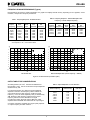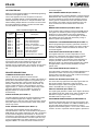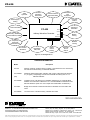
1
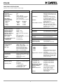
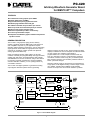
PC-420 ® ® Arbitrary Waveform Generator Board for IBM-PC/AT™ Computers INNOVATION and EXCELLENCE FEATURES • • • • • • • • • • 2 simultaneous analog outputs up to 10MHz Sample update rates to 40MHz High-resolution frequency synthesized clock Software programmable offset and gain 8 software selectable low-pass filters per channel Stores up to 32k 12-bit waveform points per channel External clock, trigger, and gate inputs Waveform repetition up to 256 or continuously TTL level synchronization output Comprehensive Windows graphic software with powerful equation resolver GENERAL DESCRIPTION The PC-420 is a high-speed, highly precise, arbitrary waveform generator board for IBM-PC/AT, PS-30, EISA bus and compatible computers. If your application requires simplicity without sacrificing performance, the PC-420 analog signal generator board offers two high-performance output channels for generating complex periodic and aperiodic analog signals simultaneously. arbitrary functions (as well as sine, square, triangle and ramp outputs) is loaded from the host computer into waveform RAM on each channel. The waveform repeat depth is programmable from 2 to 32k samples and data scans can loop up to 256 times or forever. A fixed-frequency reference clock drives a Phase Locked Loop (PLL) to minimize phase jitter, transient response, and resolution problems inherent in earlier synthesizer designs. Unlike non-buffered analog output boards, the PC-420 combines versatility and programmability with high-resolution, variable gain and phase, local data buffering and software selectable filters to result in an effective, easy-to-use solution for waveform synthesis requirements. Using PC-420GEN waveform definition software, you can quickly produce any conceivable waveform. Waveform sample points are clocked from the local buffers to a high-speed, 12-bit digital-to-analog converter stage at rates up to 40MHz. A stable internal 20MHz crystal oscillator ensures low output noise and controls waveform synthesis The PC-420 uses digital synthesis to generate the analog output signals. Waveform pattern data for generating TIMEBASE GENERATOR PC-420GEN Windows Virtual Instrument EXT. CLOCK EXT. TRIGGER Signal Files on Disk OUT1 MULTIPLYING DAC 32KS FILTERS SOFTWARE OFFSET, GAIN RING BUFFERS OUT0 MULTIPLYING DAC 32KS FILTERS CONTROL SECTION MEMORY ADDRESSING PC/AT BUS INTERFACE SAMPLE DATA DC POWER CONTROL AND DATA PC/AT Bus Figure 1. PC-420 Block Diagram 1 SYNC OUT 0 EXTERNAL TRIGGER/ GATE IN ® ® PC-420 GENERAL DESCRIPTION (Continued) by generating a 40MHz digitally synthesized sample clock source. An external trigger input synchronizes waveform scanning with your application. An external TTL “gate” input enables/disables the output channels. The sample clock can be supplied from an external source. Select or create any waveform You can select from a repertoire of standard sine, cosine, square, triangle and sawtooth waves. You can generate noise and add it to the waveform - ideal for communications circuit testing and determining the performance bounds of a system. The PC-420 generates outputs at up to 10MHz with a frequency resolution of 0.012% and ±0.012% frequency accuracy. The signal amplitude range is 20V peak to peak for squarewaves. The resolution is 0.05% of full scale at 0.1% accuracy for sine wave outputs. For non-squarewaves, the output amplitude decreases as the frequency increases. Two 12-bit DAC’s allow you to vary the offset and gain of the synthesized waveforms. The offset is adjustable from plus to minus full scale (±10V) with a 0.05% resolution while the gain is variable from ±10mV to ±10V. Equation resolver, disk files A powerful equation parser allows high speed formulation of any complex mathematical function. Upload previously created data files for regeneration by the PC-420. Waveforms may be displayed on screen before scanning and also during wave generation. The present hardware configuration can be viewed, edited, and saved to a data file for use later. Software selectable, fixed-frequency low pass anti-alias filters on each output channel ensure high spectral purity. Seven third order Butterworth low pass filters with a range of fixed cutoff frequencies from 10kHz to 10MHz (at the 3dB points), ensure proper waveform reconstruction and anti-aliasing and minimize harmonic distortion. In addition, each channel has a 20MHz low pass filter to eliminate high frequency system noise components from the output signals. Generate waveform Select the clock and trigger sources. Specify the frequency, amplitude, offset, and phase of the output signals. Choose from one of seven reconstruction filters for each of the two output channels. Start waveform generation on a single output channel or on both channels simultaneously. Software flexibility allows you to produce frequency, amplitude, phase, and burst modulated signals as well as linear and logarithmic frequency sweeps. Synthesized waveforms display the low phase noise and drift inherent to digital synthesis techniques. Wideband output amplifiers minimize distortion and exhibit excellent pulse response characteristics. Multitasking After creating a waveform and configuring the hardware you may Close the instrument panel screens and execute other applications software in the Windows environment. The predefined waveforms continue to be generated at each output channel by the PC-420, i.e. PC-420GEN continues to execute in the background. This is ideal for running long, dynamic test sequences while the host computer concurrently carries out other tasks. Simply Exit PC-420GEN when the application is complete. The PC-420 is configured on a full size PC/AT bus card that is fully contained within the host computer. Waveform and TTL level sync outputs as well as clock/trigger inputs are available on four BNC connectors mounted on the rear panel. A dual row, header connector contains 16-bit digital pattern data from channel 0. This is ideal for generating digital signals for TTL circuit test. The board is compatible with most popular programming languages and all register data is right-justified to facilitate integer data typing with high level languages such as C, FORTRAN, PASCAL, BASIC, etc. A comprehensive Users Manual is supplied with the board which details full installation, programming, and application information. Hardware test, on-line HELP Rigorous test procedures are built in to confirm proper hardware operation. Channel calibration routines are also available. A comprehensive on-line HELP engine may be invoked at any time should you have any questions related to the combined PC-420 hardware/software system. PC-420GEN - Waveform definition and generation software for Windows’. Develop custom software Easy to use instrument panel The PC-420 includes a low-level device driver library, written in C and supplied on 5.25" MS-DOS diskettes. These routines may be incorporated into user programs and used for configuring and controlling PC-420 operation. It is easy to use the PC-420 as a benchtop instrument using DATEL’s PC-420GEN waveform generation software. PC420GEN runs under Microsoft Windows 3.1 (or higher) and simulates a waveform generator instrument panel including numeric keypad, switches, slide bars, dials, buttons, etc. Although all selections can be easily made using a mouse, numbers and text may be entered from the keyboard. It is simple to use and requires no low level programming by the user. A TTL level “sync” output indicates 0V crossing on channel 0 - allowing you to phase synchronize scanning with your external hardware. Experienced programmers may obtain the complete source code listing for PC-420GEN (PC-420SRC) so they can customize it for their own applications. All hardware drivers are written in Borland C v3.1 under Microsoft Windows. The user interface is accomplished using Visual BASIC Professional. The Users Manual contains detailed register and timing information as well as example software routines to help users develop their own code. 2 ® ® PC-420 PC-420GEN Standard Waveform Panel. Select a sine, square, triangle, or sawtooth wave; specify frequency amplitude, offset and phase of the signal. Enter all data at the keypad as though it were a real instrument. Specify the reconstruction filter for each channel and turn the instrument ON to generate the waveform. Close when done, and the generated signals remain on the output channels. PC-420GEN Arbitrary Waveform Panel. Select the clock source, trigger sources and sample scan loop count. Enter the arbitrary waveform file name, load it into PC-420 waveform RAM. Specify amplitude, offset, and phase of each output waveform. Select filter and start single or dual channel scanning. Close when done, and the generated signals remain on the output channels. 3 ® PC-420 FUNCTIONAL SPECIFICATIONS (Typical at +25°C, dynamic conditions, unless noted) WAVEFORM OUTPUTS Number of Channels Amplitude Output Impedance Update Rate Offset Adjust Gain Adjust Output Protection Output Bandwidth Waveform Sine Square Ramp Triangle PC/AT BUS INTERFACE 2, non-isolated ±10V 50Ω 40MHz, maximum 12-bit unipolar DAC, adjustable from plus to minus full scale 12-bit unipolar DAC Short circuit protection to ground Architecture I/O Mapping Data Bus Max Freq. 10MHz 10MHz 100kHz 100kHz Resolution 0.012% 0.012% 0.012% 0.012% Control/Status Function OUTPUT PERFORMANCE Frequency Range Frequency Accuracy Amplitude Accuracy Loop Lock Up Time Amplitude Range Amplitude Resolution Maximum Offset Offset Resolution Sync. Output TTL Output Rise/Fall Time Gain/Offset DAC Settling Time 2.3 x 10⁻³ Hz to 10MHz ±0.012% ±0.25% of FSR 250ms +10mV to +20Vpp 0.05% of full scale (12-bit DAC) ±10V 0.05% of full scale TTL levels into 50W, on channel 0 only, active high 5 nanoseconds SQUARE WAVE 15 microseconds Sample Rate Waveform Length Vertical Resolution Rise/Fall Time Asymmetry Overshoot Rise/Fall Time Linearity Accuracy Aging 7 selectable, 1 fixed (20MHz) 10MHz, 5MHz, 1MHz 500kHz, 100kHz, 50kHz, 10kHz Software programmable 3rd order Butterworth active filters 10, 50, 100 and 500kHz. 3rd order Butterworth passive filters 1, 5, 10, and 20MHz. Operating mode 40MHz 4 to 32,768 points 12 bits (0.025% of full scale) CONNECTORS Signal Connectors 4 BNC type connectors on rear panel BNC1 Output 0 BNC2 Sync out 0 BNC3 Output 1 BNC4 External trigger/clock inputs (TTL compatible, 50Ω terminal, jumper selectable) Digital Pattern Connector 26-pin dual-row header connector mounted internally. Contains 16-bit digital data from channel 0. Strobe signal included for clocking data to external receivers. Internal or external, 40MHz max. Frequency synthesizer or 20MHz crystal clock ±50ppm (+20 to +30°C) ±5ppm/year MISCELLANEOUS WAVEFORM MEMORY Architecture Memory Capacity 40ns with 50Ω termination ±0.1% of full scale output ARBITRARY WAVEFORMS WAVEFORM CLOCK Clock Sources Internal Clock <10ns (10% to 90%) <2%, ±30ns (with 50Ω termination) <5% at full scale output (to 10MHz) RAMP, TRIANGLE AND ARBITRARY WAVEFORMS ANALOG FILTERS (EACH CHANNEL) Number of Filters Cutoff Frequency (–3dB down) Selection Filter Type I/O mapped, pluggable to IBM-PC/AT, PS-30, EISA bus and compatibles. Decodes eight 16-bit I/O registers. Decodes I/O address lines A9 through A4. A3...A0 are decoded for individual register access. Highest base address is 3F0 hex. 16-bit I/O transfers; all data is right justified, offset binary, sign-extended. Board reset, clock and trigger select, timer control, filter select, offset/gain DAC loading, frequency synthesizer control, memory select and load. Power Requirements PC/AT bus +5V PC/AT bus +12V PC/AT bus –12V Operating Temp. Range Storage Temp. Range Relative Humidity Altitude Outline Dimensions High-speed, static RAM (SRAM) 32,768k x 16 waveform samples per channel 1. Free run 2. Internal software programmable triggered 3. External trigger - TTL 4. External gate - TTL Weight 4 1.6A typical, 2.0A maximum 0.3A typical, 0.4A maximum 0.3A typical, 0.4A maximum 0 to +60°C –25 to+80°C 10% to 90%, non-condensing 0 to 10,000 feet (0 to 3047m) 4.5"H x 13.31"L x 0.5"W (11.43 x 33.81 x 1.59cm), Full size PC/AT board. Uses a single PC/AT slot. 14oz. (0.42kg) ® ® ® PC-420 FREQUENCY DOMAIN PERFORMANCE (Typical) Note: Readings are based on visual interpretation of a graphic FFT display. Results will vary depending on FFT algorithm, screen resolution, and spectrum analyzer performance. Table 2. Frequency Response - External Bandpass Filter Frequency = PC-420 Output Frequency Table 1. Frequency Response - No External Filter PC420 Output Frequency PC420 Filter Frequency Noise Floor 2nd Harmonic 3rd Harmonic 10kHz 50kHz 100kHz 500kHz 1MHz 5MHz* 10MHz* 10kHz 50kHz 100kHz 500kHz 1MHz 5MHz 10MHz –90dB –80dB –90dB –85dB –83dB –80dB –80dB –75dB –72dB –66dB –60dB –55dB –50dB –45dB –83dB –78dB –73dB –70dB –69dB –58dB –54dB PC-420 Output Frequency PC-420 Filter Frequency Noise Floor 2nd Harmonic 3rd Harmonic 98kHz 480kHz 975kHz 2.45MHz 100kHz 500kHz 1MHz 5MHz –90dB –88dB –88dB –83dB –85dB –88dB –82dB –82dB –83dB –85dB –80dB –80dB Note: Load impedance = 50Ω, internal filter enabled. Note: Load impedance = 1MΩ, internal filter enabled *Load impedance = 50Ω, internal filter enabled dB dB 0 0 0 1 0 2 4- C Py c n e u q r F = z H k 8 9 0 2 4 - C P r e tl i F = 0 1 z H k l a n r e t x E s a p d n B r e tl i F r e t n C )( y c n e u q r F = z H k 0 1 0 1 0 2 4- C P y c n e u q r F = z H k 0 1 0 2 4 - C P r e tl i F = 0 1 z H k o N l a nr et x E r e t l i F 0 2 0 2 0 3 0 3 0 4 0 4 0 5 0 5 0 6 0 6 0 7 0 7 0 8 0 8 0 9 0 9 0 1 0 1 0 04 08 021 061 02 04 2 08 2 02 3 06 3 0 04 04 08 021 061 02 04 2 08 2 02 3 06 3 04 kHz kHz No external filter External bandpass filter (center frequency = 100kHz) Figure 2. PC-420 FFT Plots (sinewave inputs) OUTPUT AMPLITUDE CONSIDERATIONS Table 3. Output Amplitude vs. Filter Selection All readings taken into a 1MΩ load with the 20MHz fixed internal filter. If a 50Ω load is connected the output amplitudes will attenuate by half. For signal frequencies up to 1MHz the output amplitude depends on the filter cutoff frequency. Table 3 reflects the output levels when the filter frequency equals the signal frequency, i.e. the full scale amplitude (±10V) is decreased by 3dB. Selecting a filter frequency higher than the output frequency will result in less attenuation but signal reconstruction quality will suffer. Above 1MHz the output amplifier’s finite bandwidth also attenuates the output signal. Conclusion: Waveform amplitude and signal quality depends on output frequency and filter selection. 5 Output Frequency Filter Frequency Amplitude (without filter) Amplitude (with filter) 10kHz 50kHz 100kHz 500kHz 1MHz 5MHz 10MHz ±10V ±10V ±10V ±10V ±10V N/A N/A ±7V ±7V ±7V ±7V ±7V ±5V ±5V ® ® PC-420 I/O REGISTER MAP Command Register. (Refer to the PC-420 User’s Manual for detailed programming information and register bit fields.) FINAL ADDRESS REGISTER (Write BASE + 2) This is selected by the Command Register. It contains the final RAM address when scanning data to the output DAC’s. When the present address is equal to this final address, the local memory pointer circulates back to the start address and the scan repeats. The number of times is specified in the Loop Count. Continuous mode is selected in the Command Register The PC-420 appears to the host computer as a set of I/O registers. The BASE address is switch selectable and can be located anywhere up to 3F0 hex on 16-byte boundaries. This allows installing multiple boards in the same host at the same time. Each individual I/O register is located at a fixed offset from this BASE as shown in Table 4. MEMORY DATA REGISTER (Read/Write BASE + 4) Table 4. PC-420 I/O Register Map I/O Address (hex) Direction BASE + 0 BASE + 0 BASE + 2 BASE + 2 BASE + 4 BASE + 6 BASE + 8 BASE + 8 BASE + A BASE + C BASE + E Write Read Write Write Write/read Write Write Write Write/read Write/read Write/read 12 bit waveform data is loaded to local PC-420 RAM through this register. The address is placed using the Start Address Register as a current address. The memory bank being accessed is selected by the Command Register. All data is right justified, raw binary data with offset binary coding to allow for bipolar output waveforms. Description Command Register Status Register Start Address Register Final Address Register Memory Data Register Frequency Synthesizer Register Filter Selection Register Loop Count Register Offset DAC Register Gain DAC Register Programmable Timer Register FREQUENCY SYNTHESIZER REGISTER (Write BASE + 6) Data for programming the frequency systhesizer counters is written to the lower 4 bits of this register. The upper 12 bits are not used. Individual counters are selected for access in the Command Register. FILTER SELECTION REGISTER (Write BASE + 8) This register selects one of seven output filters for each channel. For squarewaves the output frequency and filter selection does not effect the amplitude. However, the maximum amplitude of all waveforms varies depending on frequency and filter selections. Consult the PC-420 User Manual for details. The Filter Selection Register also enables the digital pattern outport normally disabled to minimize system noise. At power up or PC bus reset, both output channels are set to 0V. All register data is right justified and 16-bit I/O word instructions must be used to access each register. The registers may be programmed in any sequence as long as the Command Register bits that enable the outputs are written last. LOOP COUNT REGISTER (Write BASE + 8) This 8-bit register is selected by the Command Register and it specifies the number of times to loop in local RAM when scanning data to the DAC’s (up to 256). Continous scanning is selected by the Command Register. REGISTER DESCRIPTIONS COMMAND REGISTER (Write BASE + 0) This is a 16-bit wide register that controls PC-420 programming and controls operation. It allows host software to specify other local hardware registers for programming or for reading status information. These include the filter register selection, offset and gain DAC selection, 82C54 timer, and memory register selections. It also specifies the clock and trigger sources, i.e., internal or external. When ready to start generating waveforms from local RAM, the Command Register enables the output channels - individually or simultaneously. OFFSET DAC REGISTER (Write BASE + A) This 12 bit write only register sets the output signal offset. All data is right justified, offset binary coding for bipolar selections. The upper 4 bits in the register are not used. The offset is selectable within a range of ±10V. GAIN DAC REGISTER (Write BASE + C) The output signal gain data is written to this register. All data is right justified 12-bit data, offset binary coding for bipolar gain selections. The upper 4 bits are not used. The gain is selectable within a range of ±10V. STATUS REGISTER (Read BASE+ 0) The Status Register resides at the same I/0 address location as the Command Register but it displays a different bit representation. It is read only and it reports the output channel level (with respect to 0V) and echoes the status of the phase locked loop section. PROGRAMMABLETIMER REGISTER (Read/Write BASE + E) The 82C54 programmable timer sets the internal trigger rate and the DAC clock rate (based on a 10MHz oscillator input). It is a byte-wide (8-bit) register that contains one Control Register and three data registers - one for each of three 16-bit counters. Access to a particular internal register is specified in START ADDRESS REGISTER (Write BASE + 2) This register must be loaded with the start address in waveform RAM for a data scan. It also doubles as the present RAM address when loading signal files from disk. It is selected by the Command Register. Local hardware on the PC-420 compares the start (present) and final register contents during a scan and restarts the waveform scan when equal. The loop count is programmable up to 256 by writing the Loop Count Register at BASE + 8. Continuous mode is selected in the 6 ® ® PC-420 Note: Waveform data must be uploaded from disk file to PC420 RAM before starting generation. Data cannot be uploaded from disk while DAC’s are clocking. the Command Register. Detailed programming and timing information is available in the PC-420 User’s Manual. PROGRAMMING SEQUENCE SIGNAL DATA FILES PC-420GEN provides all the waveform creation, upload, and generation facilities without any low level programming by the user. However, custom applications may require some software development - either modification of PC-420SRC or complete hardware coding. The low level driver library supplied with PC-420 will be very helpful when writing code. Waveform data must be loaded from disk file to local RAM on each PC-420 channel before scanning. All data must be 12 bits wide, right justified raw binary data with offset binary coding to allow for bipolar output ranges. It may be created mathematically by host software or generated by an AID board e.g., DATEL’s PC-414 fast analog input board. The following flow diagram illustrates PC-420 programming strategy. Complete programming details and example code listings are in the PC-420 User’s Manual. The file can be uploaded to the PC-420 RAM using most high level programming languages that can do I/O accesses, e.g. “C”, BASIC, FORTRAN, etc. This is done through the Memory Data Register at BASE + 4. Individual addresses are specified in the Start Address Register at BASE + OAh. No hardware configuration header information can be included unless host software strips it from the signal data before loading. Scan modes and scan rates can be programmed directly by host software. START Note: PC-420GEN contains a powerful equation parser that will resolve and evaluate any complex waveform equation entered by the user. The parser will then generate the appropriate data file. PC-420GEN uploads this data file to local waveform RAM and generates the desired waveform. A waveform plotting utility in PC-420GEN allows you to confirm proper signals before scanning. Program Frequency Synthesizer Registers Program 82C54 Timer • Internal Trigger Rate • DAC Clock Rate The PC-420 waveform RAM repeat depth is programmable from 4 to 32,768 samples by setting the Start and Final memory addresses. Data scanning can loop on this up to 256 times or continuously - a non-stop “forever’ mode. The loop count is programmable via the Loop Count Register at BASE+ 8. Continuous mode is selected in the Command Register. Select Start/Final RAM Addresses, Upload Signal Data File Specify Loop Count (3 to 256) or Continuous by Writing Command Register Loop Counter (up to 256 times or "forever") Command Register selects different registers for access. 0 Start Address Write Gain and Offset DAC Registers Final Address Signal File Data Select one of 7 filters for each output channel Waveform Memory 32,768 samples Empty - no data Figure 3. PC-420 Waveform Buffer Scanning One period of a waveform only needs to be loaded to PC-420 RAM. By looping on this, a continuous waveform may be generated. Be aware that concatenated data files and truncated waveforms can be discontinuous at their boundaries - resulting in glitches in the output signals. A graphic waveform editor is the ideal solution to smoothing such files before loading them to the PC-420. Start Waveform Generation • Select Clock Source • Select Continuous Scanning • Enable Outputs END Figure 2. PC-420 Programming Flow Chart 7 ® ® PC-420 Audio Synthesis Intricate Waveform Generation Communications Signal Simulation Automatic Test Equipment Complex Motion Controllers Power Supply Testing Pulse Generation PC-420 Arbitrary Waveform Generator Telemetry, Satellite, Communications, Radar Transducer Simulation OUT0 SYNC Modem Testing OUT1 TRIG/CLK Frequency Response Measurements Material Testing Bio-medical Simulation Digital Circuit Testing Modulation PSK, FSK Generate Circuit Stimuli Figure 4. PC-420 Applications ORDERING INFORMATION Model Description PC-420 Arbitrary waveform generator board. Includes a comprehensive user manual and low level device driver library on MS-DOS diskettes. PC-420GEN Waveform definition/generation software utility, written under Microsoft Windows 3.1 (or higher). This package includes the executable and library files on 3.5" MS-DOS diskettes. (HD) PC-420SRC Complete source code listing for PC-420GEN. Supplied on 3.5" (HD) MS-DOS diskettes. All code written in Borland C v3.1 and Visual BASIC Professional under Microsoft Windows. (Note: You must compile with Visual BASIC Professional.) PC-420LV Bridge driver software to National Instruments’ LabVIEW®. See PC-420LV data sheet. PC-420DRV Low level source code driver library, included with board. IBM-PC/AT is an IBM Corporation trademark. Windows is a Microsoft Corporation trademark. LabVIEW is a National Instruments trademark. ® ® DATEL, Inc. 11 Cabot Boulevard, Mansfield, MA 02048-1194 Tel: (508) 339-3000 / Fax: (508) 339-6356 For immediate assistance 1-800-233-2765 DATEL DATEL DATEL DATEL (UK) LTD. Tadley, England Tel: (01256)-880444 S.A.R.L. Montigny Le Bretonneux, France Tel: 1-34-60-01-01 GmbH Munchen, Germany Tel: 89-544334-0 KK Tokyo, Japan Tel: 3-3779-1031, Osaka Tel: 6-354-2025 DATEL makes no representation that the use of its products in the circuits described herein, or the use of other technical information contained herein, will not infringe upon existing or future patent rights. The descriptions contained herein do not imply the granting of licenses to make, use, or sell equipment constructed in accordance therewith. Specifications are subject to change without notice. The DATEL logo is a registered DATEL, Inc. trademark.