1
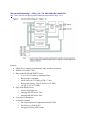
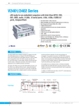
DigilentNexys™3Spartan‐6FPGABoardNotes
http://www.digilentinc.com/Products/Detail.cfm?NavPath=2,400,897&Prod=NEXYS3
IC: Xilinx Spartan®-6 FPGA (XC6LX16-CS324)
Programming: Digilent USB2 port providing board power, programming, & data transfers
Connector(s):
Digilent USB2 port
USB 2.0 port,
High-speed 40-pin VHDC expansion connector,
Four 12-pin Pmod™ connectors,
VGA, and
10/100 Ethernet
Board Features
100MHz fixed-frequency oscillator
Xilinx Spartan6 XC6LX16-CS324
16Mbyte Micron Cellular RAM
16Mbyte Micron Parallel PCM
16Mbyte Micron Quad-mode SPI PCM
10/100 SMSC LAN8710 PHY
8 slide switches, 5 push buttons, 4-digit 7seg display, 8 LEDs
Type-A USB host for mouse, keyboard or memory stick
USB-UART
Digilent Adept USB port for power, programming & data transfers
8-bit VGA
Four double-wide Pmod™ connectors, one VHDC connector
CellularRAM—http://www.cellularram.com/
The Technology
CellularRAM is a multi-generation family of low-power pseudo-static RAM (PSRAM)
for wireless handsets. CellularRAM memory is designed to meet the growing memory
and bandwidth demands of future handset designs. In addition to offering a lower cost/bit
ratio than current solutions, this type of Pseudo SRAM features a SRAM-pin
compatibility, refresh-free operation and a low-power design.
Compatibility:
Asynchronous CellularRAM devices are backward compatible with standard SRAM
devices. They have the same voltage range, package, and ball assignment. Designers will
have a smooth transition from SRAM to CellularRAM.
Power Consumption:
While CellularRAM is based on DRAM technology, the power consumption is
comparable to SRAM devices.
Innovative Interface:
The CellularRAM family supports asynchronous/page modes, as well as an innovative
burst interface that is fully compatible with the low-power Flash interface.
Performance:
The asynchronous/page version access time target is 70ns. CellularRAM with burst
access mode will support a burst rate of up to 133 MHz.
Cost:
The price/bit of CellularRAM will be significantly lower than an SRAM device with a
corresponding density and technology node.
http://www.cellularram.com/about/index.html
Micron PSRAM/CelluarRAM
Merging the Best of DRAM and SRAM
CellularRAM® memory is a pseudo-static DRAM (PSRAM) device that features an
SRAM-like architecture, hidden refresh operation, and SRAM pin-compatibility. This
hybrid memory delivers the best of SRAM and DRAM features, combining low power
consumption and high-speed read and write functions. Because CellularRAM memory
also offers synchronous operations, fast access, and variable latency initial burst access,
you get high throughput and excellent performance. It's an ideal solution for low-power,
space-limited designs like MCPs, as well as mobile and industrial applications.
http://www.micron.com/products/dram/psram-cellularram
http://www.micron.com/~/media/Documents/Products/Technical%20Note/DRAM/tn4530_psram_101.pdf
Review in class
Technical Note, PSRAM 101: An Introduction to Micron® CellularRAM® and PSRAM
http://www.micron.com/~/media/Documents/Products/Technical%20Note/DRAM/tn4530_psram_101.pdf
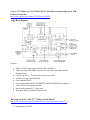
Configurations
Figures 2 Async/Page Functional Block Diagram
Figure 3 Async/Page/Burst Functional Block Diagram, and
Figure 4 Burst AD-Mux Functional Block Diagram
Storage Cell Comparison
Figure 5: SRAM Storage Cell
Figure 6: The 1T/1C DRAM Storage Cell Array
Figure 7: DRAM Sense Amp
Figure 8: 1T/1C Illustration
Figure 10: 2T/2C Sensing Scheme
Basic Operations for Broadside (Parallel) Addressing (p. 10-13)
Setting the Configuration Registers (p. 19)
Two basic methods are available to access the configuration registers: configuration
register access using CRE and software access.
Technical Note, Variable vs. Fixed Latency CellularRAM™ Operation
http://www.micron.com/~/media/Documents/Products/Technical%20Note/DRAM/tn4522.pdf
Also useful
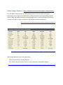
Micron mt45w8mw16bgx: 8 Meg x 16 – 128 Mbit PSRAM/CelluarRAM
http://www.micron.com/parts/psram/cellularram/mt45w8mw16bgx-701-it
Features
Single device supports asynchronous, page, and burst operations
Random access time: 70ns
Burst mode READ and WRITE access
• 4, 8, 16, or 32 words, or continuous burst
• Burst wrap or sequential
• MAX clock rate: 133 MHz (tCLK = 7.5ns)
• Burst initial latency: 35ns (5 clocks) at 133 MHz
• tACLK: 5.5ns at 133 MHz
Page mode READ access
• Sixteen-word page size
• Interpage READ access: 70ns
• Intrapage READ access: 20ns
Low power consumption
Low-power features
• On-chip temperature-compensated refresh (TCR)
• Partial-array refresh (PAR)
• Deep power-down (DPD) mode
Data sheet review
http://www.micron.com/products/dram/psram-cellularram#fullPart&236=3
Bus Operating Modes (p. 10-14)
Registers (p. 17-23)
Initial Access Latency (BCR[14]) Default = Variable
We have -70XX … (XX=1, I think. Therefore -701 above and CLK >=100 MHz.)
From starting to look at configurations, I believe the clock is not being used, connected to
ground.
Timing diagrams start on page 41.
Tables for the timing values start on page 37.
PhaseChangeMemory‐http://www.micron.com/products/phase‐change‐memory
Our P8P phase change memory (PCM) combines the best traits of traditional memory
technologies into a single, nonvolatile device with a performance-boosting parallel interface.
Ideal for high-end high performance embedded applications; second-generation P8P products
increase performance, improve endurance, and simplify software management.
http://www.micron.com/products/phase-change-memory/parallel-pcm
http://www.micron.com/~/media/Documents/Products/White%20Paper/pcm_enables_new_memory_usage_models.pdf
Marketing Information on use and application:
The Evolution of Phase Change Memory
Why PCM is Ready for Prime Time as a Next-Generation, Nonvolatile Memory
http://www.micron.com/~/media/Documents/Products/White%20Paper/evolution_of_phase_change_memory.pdf
Micron np8p128a13t1760: 128 Mbit P8P Parallel Phase Change Memory (PCM)
http://www.micron.com/parts/pcm/parallel-pcm/np8p128a13t1760e
Features
High-performance READ
• 115ns initial READ access
• 135ns initial READ access
• 25ns, 8-word asynchronous-page READ
Architecture
• Asymmetrically blocked architecture
• Four 32KB parameter blocks with top or bottom configuration
• 128KB main blocks
• Serial peripheral interface (SPI) to enable lower pin count on-board programming
Phase change memory (PCM)
• Chalcogenide phase change storage element
• Bit-alterable WRITE operation
Simplified software management
• No block erase or cleanup required
• Bit twiddle in either direction (1:0, 0:1)
• 35μs (TYP) PROGRAM SUSPEND
• 35μs (TYP) ERASE SUSPEND
• Flash data integrator optimized
• Scalable command set and extended command set compatible
• Common Flash interface capable
Data Sheet
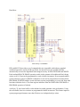
from Nexys 3 Schematic
P8P parallel PCM provides a set of commands that are compatible with industry-standard
command sequences used by NOR-type Flash. An internal write state machine (WSM)
automatically executes the algorithms and timings necessary for BLOCK ERASE and WRITE.
Each emulated BLOCK ERASE operation results in the contents of the addressed block being
written to all 1s. Data can be programmed in word or buffer increments. Erase suspend enables
system software to pause an ERASE command so it can read or program data in another block.
PROGRAM SUSPEND enables system software to pause programming so it can read from other
locations within the device. The status register indicates when the WSM’s BLOCK ERASE or
PROGRAM operation is finished.
A 64-byte, 32 word write buffer is also included to enable optimum write performance. Using
the write buffer, data is overwritten or programmed in buffer increments. This feature improves
system program performance more than 20 times over independent byte writes.
Timing diagrams start on page 50.
Tables for the timing values start on page 49.
WE# appears to write configuration and then the data to be stored.
PhaseChangeMemory‐http://www.micron.com/products/phase‐change‐memory
The P5Q PCM is purpose-built to meet the memory requirements of embedded systems,
delivering multiple I/O capability and compatibility via familiar SPI NOR interfaces. P5Q
improves overall performance and enables software simplification using byte-alterability
(overwrite capability). It also increases system-level reliability by delivering 1 million writecycle endurance (compared to 100,000 for NOR flash)..
http://www.micron.com/products/phase-change-memory/serial-pcm
Micron NP5Q128A13E: 128Mb P5Q Serial Phase Change Memory (PCM)
http://www.micron.com/parts/pcm/serial-pcm/np5q128a13esfc0e?pc={DE63C83A-B049-44B6-8424-1963A6B75C54}
Features
SPI bus compatible serial interface
Maximum clock frequency: – 66 MHz (0°C to +70°C) or 33 MHz (–30°C to +85°C)
Supports legacy SPI protocol and new quad I/O or dual I/O SPI protocol
Quad I/O frequency of 50 MHz, resulting in an equivalent clock frequency up to 200
MHz
Dual I/O frequency of 66 MHz, resulting in an equivalent clock frequency up to 132
MHz
Continuous READ of entire memory via single instruction:
WRITE operations
o 128Kb sectors ERASE (emulated)
o Legacy Flash PAGE PROGRAM
o Bit-alterable page WRITEs
o PAGE PROGRAM on all 1s (PRESET WRITEs)
Write protections: protected area size defined by four nonvolatile bits
(BP0, BP1, BP2, and BP3)
JEDEC-standard two-byte signature (DA18h)
Uniform 128Kb sectors (Flash emulation)
128Mb density with SOIC16 package
More than 1,000,000 WRITE cycles
Phase change memory (PCM): Chalcogenide phase change storage element
Nexys 3 User’s Manual
http://www.micron.com/~/media/Documents/Products/Data%20Sheet/PCM/p5q_32_64_128Mb_serial_pcm_ds.pdf
Notice: The board is operating in Quad mode … 4-bit I/O for each IC.
SPI Data Transfer Example
http://www.micron.com/~/media/Documents/Products/Data%20Sheet/PCM/p5q_32_64_128Mb_serial_pcm_ds.pdf
Quad SPI Data Transfer Example
http://www.micron.com/~/media/Documents/Products/Data%20Sheet/PCM/p5q_32_64_128Mb_serial_pcm_ds.pdf
Quad SPI Data Transfer Example
http://www.micron.com/~/media/Documents/Products/Data%20Sheet/PCM/p5q_32_64_128Mb_serial_pcm_ds.pdf
Timing diagrams start on page 38.
Tables for the timing values start on page 37.
Note: For all instrutions, maximum clock rate is 33 MHz or approximately 30 nsec.
SMSC LAN8710Ai-EZK: Small Footprint MII/RMII 10/100 Ethernet Transceiver with
HP Auto-MDIX and flexPWR® Technology
http://www.smsc.com/LAN8710
Features
Single-Chip Ethernet Physical Layer Transceiver (PHY)
HP Auto-MDIX support
Small footprint 32-pin QFN lead-free RoHS compliant package (5 x 5 x 0.9mm height)
High-Performance 10/100 Ethernet Transceiver
o Compliant with IEEE802.3/802.3u (Fast Ethernet)
o Compliant with ISO 802-3/IEEE 802.3 (10BASE-T)
o Loop-back modes
o Auto-negotiation
o Automatic polarity detection and correction
o Link status change wake-up detection
o Vendor specific register functions
o Supports both MII and the reduced pin count RMII interfaces
Cypress CY7C68013A-56: EZ-USB® FX2LP™ USB Microcontroller High-Speed USB
Peripheral Controller
http://www.cypress.com/?mpn=CY7C68014A-56PVXC
Features:
USB 2.0 USB IF high speed certified (TID # 40460272)
Single chip integrated USB 2.0 transceiver, smart SIE, and enhanced 8051
microprocessor
Ultra low power: ICC No more than 85 mA in any mode
16 KB of on-chip code/data RAM
Four integrated FIFOs
Four programmable BULK, INTERRUPT, and ISOCHRONOUS endpoints
8-bit or 16-bit external data interface
Smart media standard ECC generation
Integrated, industry standard enhanced 8051
Microchip 24AA128: 128K I2C™ CMOS Serial EEPROM
http://www.microchip.com/wwwproducts/Devices.aspx?dDocName=en010781
programming for USB
FTDI FT232R: USB UART IC
http://www.ftdichip.com/Products/ICs/FT232R.htm
Features
Single chip USB to asynchronous serial data transfer interface.
Entire USB protocol handled on the chip. No USB specific firmware programming
required.
Fully integrated 1024 bit EEPROM storing device descriptors and CBUS I/O
configuration.
Fully integrated USB termination resistors.
Fully integrated clock generation with no external crystal required plus optional clock
output selection enabling a glue-less interface to external MCU or FPGA.
Data transfer rates from 300 baud to 3 Mbaud (RS422, RS485, RS232 ) at TTL levels.
128 byte receive buffer and 256 byte transmit buffer utilising buffer smoothing
technology to allow for high data throughput.
FTDI‟s royalty-free Virtual Com Port (VCP) and Direct (D2XX) drivers eliminate the
requirement for USB driver development in most cases
UART interface support for 7 or 8 data bits, 1 or 2 stop bits and odd / even / mark / space
/ no parity
FIFO receive and transmit buffers for high data throughput.
Microchip PIC24/32 (?)
from reference manual PIC24FJ192:
http://www.microchip.com/pagehandler/en-us/family/16bit/architecture/pic24f.html
Driver/Controller for USB A port
Oasistek tof-2481BE-N 7-Segment Display:
http://www.oasistek.com.tw/en/pro-led.php
Common cathode (?) multiplexed displays