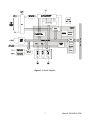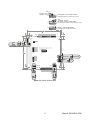
1
10623 Roselle Street, San Diego, CA 92121 y (858) 550-9559 y Fax (858) 550-7322
[email protected] y www.accesio.com
MODEL 104-AIO16-16W
USER MANUAL
FILE: M104-AIO1616W.I4j
Notice
The information in this document is provided for reference only. ACCES does not assume any liability arising out
of the application or use of the information or products described herein. This document may contain or
reference information and products protected by copyrights or patents and does not convey any license under
the patent rights of ACCES, nor the rights of others.
IBM PC, PC/XT, and PC/AT are registered trademarks of the International Business Machines Corporation.
Printed in USA. Copyright 2005 by ACCES I/O Products, Inc. 10623 Roselle Street, San Diego, CA 92121-1506.
All rights reserved.
WARNING!!
ALWAYS CONNECT AND DISCONNECT YOUR FIELD CABLING WITH THE
COMPUTER POWER OFF. ALWAYS TURN COMPUTER POWER OFF
BEFORE INSTALLING A BOARD. CONNECTING AND DISCONNECTING
CABLES, OR INSTALLING BOARDS INTO A SYSTEM WITH THE
COMPUTER OR FIELD POWER ON MAY CAUSE DAMAGE TO THE I/O
BOARD AND WILL VOID ALL WARRANTIES, IMPLIED OR EXPRESSED.
2
Manual 104-AIO16-16W
Warranty
Prior to shipment, ACCES equipment is thoroughly inspected and tested to applicable specifications. However,
should equipment failure occur, ACCES assures its customers that prompt service and support will be available.
All equipment originally manufactured by ACCES which is found to be defective will be repaired or replaced
subject to the following considerations.
Terms and Conditions
If a unit is suspected of failure, contact ACCES' Customer Service department. Be prepared to give the unit
model number, serial number, and a description of the failure symptom(s). We may suggest some simple tests
to confirm the failure. We will assign a Return Material Authorization (RMA) number which must appear on the
outer label of the return package. All units/components should be properly packed for handling and returned
with freight prepaid to the ACCES designated Service Center, and will be returned to the customer's/user's site
freight prepaid and invoiced.
Coverage
First Three Years: Returned unit/part will be repaired and/or replaced at ACCES option with no charge for labor
or parts not excluded by warranty. Warranty commences with equipment shipment.
Following Years: Throughout your equipment's lifetime, ACCES stands ready to provide on-site or in-plant
service at reasonable rates similar to those of other manufacturers in the industry.
Equipment Not Manufactured by ACCES
Equipment provided but not manufactured by ACCES is warranted and will be repaired according to the terms
and conditions of the respective equipment manufacturer's warranty.
General
Under this Warranty, liability of ACCES is limited to replacing, repairing or issuing credit (at ACCES discretion)
for any products which are proved to be defective during the warranty period. In no case is ACCES liable for
consequential or special damage arriving from use or misuse of our product. The customer is responsible for all
charges caused by modifications or additions to ACCES equipment not approved in writing by ACCES or, if in
ACCES opinion the equipment has been subjected to abnormal use. "Abnormal use" for purposes of this
warranty is defined as any use to which the equipment is exposed other than that use specified or intended as
evidenced by purchase or sales representation. Other than the above, no other warranty, expressed or implied,
shall apply to any and all such equipment furnished or sold by ACCES.
3
Manual 104-AIO16-16W
Table of Contents
Chapter 1: Introduction ......................................................................................................... 6
Figure 1-1: Block Diagram ............................................................................................................................. 7
Chapter 2: Installation........................................................................................................... 8
Figure 2-1: PC/104 Key Information .............................................................................................................. 9
Chapter 3: Option Selection ............................................................................................... 10
Figure 3-1: Option Selection Map ................................................................................................................ 11
Table 3-1: Hex Conversion .......................................................................................................................... 12
Table 3-2: Jumper Configuration.................................................................................................................. 13
IRQ Configuration ........................................................................................................................................... 13
DAC Configuration.......................................................................................................................................... 14
A/D Configuration ........................................................................................................................................... 15
Table 3-3: Range Selection ......................................................................................................................... 15
Chapter 4: Analog/Digital Converter Operation ................................................................ 17
Overview: A/D Operational Modes ................................................................................................................ 17
Breakdown: A/D Operational Modes............................................................................................................. 17
Step-By-Step: A/D Operational Modes ......................................................................................................... 18
1.
Software Step-by-Step....................................................................................................................... 18
2.
Burst Mode Step-By-Step.................................................................................................................. 18
3.
Triggered (TIMED) Step-By-Step ...................................................................................................... 19
READ DATA FAST........................................................................................................................................... 19
Chapter 5: Digital Input/Output .......................................................................................... 21
Chapter 6: Programming .................................................................................................... 22
Base Address + 0 - Start A/D Conversion (Write).................................................................................... 23
Base Address + 0 - Read A/D Data FIFO (Word Read)............................................................................ 23
Base Address + 1 - A/D Data FIFO Reset ................................................................................................. 23
Base Address + 2 - A/D Channel Scan Control (Write only) .................................................................. 23
Base Address + 3 - A/D Burst Mode Control (Write Only)...................................................................... 24
Base Address + 4 - Software Programmable Gain Select 0-7 (Word Write) ......................................... 24
Base Address + 6 - Software Programmable Gain Select 8-15 (Word Write) ....................................... 24
Base Address + 7 - A/D Software Gain Reset (Read).............................................................................. 24
Base Address + 8 - DAC 0 (Word Write)................................................................................................... 24
Base Address + 8 - Jumper Configuration / Status (Read) .................................................................... 25
Base Address + 9 - Internal Status Register (Read) ............................................................................... 25
Base Address + A - EEPROM Data Write and Read................................................................................ 25
Writing to the EEPROM .................................................................................................................................. 26
Reading from the EEPROM............................................................................................................................ 27
Base Address + A - A/D Channel Read (Bits 3 - 0).................................................................................. 28
Base Address + B - Calibration Data Write .............................................................................................. 28
Base Address + C - Interrupt Enable (Write Only) .................................................................................. 29
Base Address + D - A/D Format Select (Write Only) ............................................................................... 29
Base Address + E - DAC 1 (Word Write) .................................................................................................. 29
Base Address + 10 - Digital I/O Bits 0 - 7 ................................................................................................. 29
Base Address + 11 - Digital I/O Bits 8 - 15 ............................................................................................... 30
Base Address + 14 through Base Address + 17 - Counter Programming ............................................ 30
Base Address + 18 - DAC Mode Select (Write) ........................................................................................ 30
Base Address + 19 - Reset Digital I/O to Input Mode (Write) ................................................................. 30
Base Address + 1A - Configure Oversampling (Write Only) .................................................................. 30
Base Address + 1B - A/D Counter Trigger Select (Write Only) .............................................................. 31
Base Address + 1C - EXTERNAL TRIGGER Selection ( Write Only) ..................................................... 31
Base Address + 1D - Board Reset (Read) ................................................................................................ 31
Base Address + 1E - Enable Counters (Write Only)................................................................................ 31
Chapter 7: Connector Pin Assignments............................................................................ 32
Connector P1, 26-pin IDC header male MUX Inputs, DAC Outputs...................................................... 32
Connector P2, 34-pin IDC Header Male Digital I/O .................................................................................. 33
Connector “L”, 8-pin IDC Header Male..................................................................................................... 33
4
Manual 104-AIO16-16W
Connector P3, 8-pin IDC Header Male ...................................................................................................... 34
Appendix A: Technical Specifications............................................................................... 35
Appendix B: 82C54 Counter Timer Operation................................................................... 36
OPERATIONAL MODES.................................................................................................................................. 36
Mode 0: Pulse on Terminal Count............................................................................................................. 36
Mode 1: Retriggerable One-Shot............................................................................................................... 36
Mode 2: Rate Generator ............................................................................................................................. 36
Mode 3: Square Wave Generator .............................................................................................................. 36
Mode 4: Software Triggered Strobe.......................................................................................................... 36
Mode 5: Hardware Triggered Strobe......................................................................................................... 37
PROGRAMMING .............................................................................................................................................. 38
READING AND LOADING THE COUNTERS ................................................................................................. 39
Appendix C: Calibration...................................................................................................... 41
Overview: Calibrating without using the provided calibration program................................................... 42
Breakdown: Calibrating the DACs ................................................................................................................ 42
Step 1.
Determine the Calibration Constants for the DAC................................................................. 42
Step 2.
Write the Calibration Constants into the Calibration Potentiometers ................................. 42
Step-By-Step: Calibrating the DACs ............................................................................................................. 43
Breakdown: Calibrating the A/D .................................................................................................................... 43
Step 1.
Determine the Calibration Constants for the A/D .................................................................. 44
Step 2.
Write the Calibration Constants into the Calibration Potentiometers ................................. 44
Step-By-Step: Calibrating the A/D................................................................................................................. 44
Step 1.
Determine the Calibration Constants for the A/D .................................................................. 44
Step 2.
Write the Calibration Constants into the Calibration Potentiometers ................................. 45
Table C-1: Factory EEPROM Calibration Locations.................................................................................... 46
5
Manual 104-AIO16-16W
Chapter 1: Introduction
This board is a high-speed, multifunction board featuring an excellent price/performance value. It is very
useful for precision PC/104-based data acquisition, control, or signal analysis in applications such as
standalone environmental test stations, compact production test equipment, portable testers, avionics
and others. In addition to direct data transfers, the board's ability to trigger the A/D in real time assures
synchronized sampling that is unaffected by other computer operations. This is an essential requirement
for signal, vibration and transient analysis where high data rates must be sustained for short periods of
time. This high-speed sampling rate is supported by a FIFO for reducing processor overhead and is
filtered for an extremely quiet front end. Sixteen parallel bits of digital I/O and two D/A outputs allow for a
complete, high-performance data acquisition solution.
Analog Input
16 (Single-Ended) or 8 (Differential) 16-Bit Analog Inputs are provided. Any single channel can be
acquired at 500,000 samples / second, or any range of channels can be acquired at 450,000 samples /
second. The Analog Inputs feature hardware / software selectable ranges of 0-1V, 0-2V, 0-4V, 0-5V, 010V, ±0.5V, ±1V, ±2V, ±2.5V, ±5V, and ±10V. All the data from the A/D is placed in a 1KSample FIFO
for the fastest possible data transfer. Conversions can be started by the board using an internal burst
mode, or via the counter.
Analog Output
Two 12-Bit Digital-to-Analog converter outputs are provided. Output ranges of 0-5V and 0-10V are field
selectable with jumpers, per channel.
Digital I/O
16 Buffered Digital Input/Outputs are provided. All 16 lines may be programmed as inputs or outputs or
8 lines may be inputs while the other 8 are outputs. All lines are pulled up to 5 Volts.
Counter/Timer
The board uses an 82C54 Programmable Interval Timer (3 sixteen bit counters). The counters are
generally used to time various aspects of the A/D conversion process, but can be used for frequency
generation. Consult Chapter 4, Chapter 6, and Appendix B for more information on the A/D,
programming, and the counter itself.
Calibration
This board features digitally controlled potentiometers which are used to adjust the gain and offset of
the A/D function and the gain of the DAC function. This allows both the analog inputs and outputs to be
calibrated from software in the field.
In order to obtain accurate data, the proper values must be loaded into the digital potentiometers each
time the board is powered. If no constants are loaded, the potentiometers will power-on to the center of
their ranges, which will result in a non- or poorly-calibrated situation. The calibration values are stored in
an on-board EEPROM allowing simple re-use of calibration data from one boot to the next.
For details refer to Chapter 6 on programming, and Appendix C on Calibration.
6
Manual 104-AIO16-16W
Figure 1-1: Block Diagram
7
Manual 104-AIO16-16W
Chapter 2: Installation
ENSURE YOU HAVE APPROPRIATE POWER IN YOUR PC/104 STACK TO OPERATE THE BOARD! It
requires +5V, +12V, and -12V to operate properly unless you purchased the board with a DC/DC
converter. The paper label on the board will indicate -DC if a DC/DC converter is installed on the board.
The DC requires only +5V power.
A printed Quick-Start Guide (QSG) is packed with the board for your convenience. If you’ve already performed
the steps from the QSG, you may find this chapter to be redundant and may skip forward to begin developing
your application.
The software provided with this PC/104 Board is on CD and must be installed onto your hard disk prior to use.
To do this, perform the following steps as appropriate for your operating system. Substitute the appropriate drive
letter for your CD-ROM where you see d: in the examples below.
CD Installation
The following instructions assume the CD-ROM drive is drive “D”. Please substitute the appropriate drive letter
for your system as necessary.
DOS
1.
Place the CD into your CD-ROM drive.
2.
Type B- to change the active drive to the CD-ROM drive.
3.
4.
Type GLQR?JJ- to run the install program.
Follow the on-screen prompts to install the software for this board.
WINDOWS
1.
Place the CD into your CD-ROM drive.
2.
The system should automatically run the install program. If the install program does not run promptly,
click START | RUN and type BGLQR?JJ, click OK or press -.
3.
Follow the on-screen prompts to install the software for this board.
LINUX
1.
Please refer to linux.htm on the CD-ROM for information on installing serial ports under linux.
8
Manual 104-AIO16-16W
Installing the Hardware
Before installing the board, carefully read Chapter 3 and Chapter 4 of this manual and configure the board
according to your requirements. The SETUP Program can be used to assist in configuring jumpers on the
board. Be especially careful with Address Selection. If the addresses of two installed functions overlap, you will
experience unpredictable computer behavior. To help avoid this problem, refer to the FINDBASE.EXE program
installed from the CD. The setup program does not set the options on the board, these must be set by jumpers.
To Install the Board
1.
2.
3.
4.
5.
6.
7.
Install jumpers for selected options and base address according to your application
requirements, as mentioned above.
Remove power from the PC/104 stack.
Assemble standoff hardware for stacking and securing the boards.
Carefully plug the board onto the PC/104 connector on the CPU or onto the stack, ensuring
proper alignment of the pins before completely seating the connectors together.
Install I/O cables onto the board’s I/O connectors and proceed to secure the stack together or
repeat steps 3-5 until all boards are installed using the selected mounting hardware.
Check that all connections in your PC/104 stack are correct and secure then power up the
system.
Run one of the provided sample programs appropriate for your operating system that was
installed from the CD to test and validate your installation.
Figure 2-1: PC/104 Key Information
9
Manual 104-AIO16-16W
Chapter 3: Option Selection
Jumpers are available on the board to setup the following selections:
Base address
IRQ level
DAC output voltage ranges
A/D input mode (single ended or differential) and range
Please refer to the Setup Program on the Software Master CD for details of selecting the appropriate options for
your application.
The standard board has a Counter/Timer Chip, two 12-bit DAC Channels, 16 Bits of Digital I/O, and a 16
channel 16-bit A/D Converter.
There is an optional version of the board that provides an onboard DC/DC converter. If your PC/104 stack has
+5V and +/-12V available, a DC/DC converter is not needed.
10
Manual 104-AIO16-16W
GND - 34
EXTERNAL
TRIGGER - 33
40 EXTERNAL SCAN START MODE
39 (USES EXT SIGNAL TO START EACH SCAN)
P2
34 - GND
36 - EXTERNAL TRIGGER
P2
40 DELAYED START, TIMED MODE
39 (WAITS FOR EXT SIGNAL, THEN USES 8254 CTR)
P2
40 TIMED SCAN START MODE
39 (USES 8254 CTR TO TIME A/D SCANS)
P2
Pin 1
P3
EXT-P3
IRQ10
IRQ11
IRQ12
IRQ14
IRQ15
BIPOLAR
IRQ7
IRQ6
IRQ5
IRQ4
IRQ3
GNH
UNIPOLAR
GNL
P1
DAC A
DAC B
Pin 1
±12V SOURCE SELECT
A5
A6
A7
A8
A9
DC/DC Option 104 Bus
IRQ9
0-10V
0-5V
DIFF
S.E.
Figure 3-1: Option Selection Map
11
Manual 104-AIO16-16W
Address Selection
The Board’s Base Address is set by jumpers labeled “BOARD ADDR.” The jumpers are marked /A5 through
/A9, and /A5 is the least significant bit of the address. The base addresses can be selected anywhere within the
I/O address range 000-3E0 provided that they do not overlap with other functions. The FINDBASE software
utility provided on the CD with your board will help you select a base address that does not conflict with other
assignments.
This board requires a block of 32 addresses (20 hex). Address Setup Jumper locations are marked /A5 through
/A9. In order to configure the desired address, the hexadecimal address must be converted to a binary
representation, which is then selected by installing jumpers on the board.
For example, as illustrated below, switch selection corresponds to hex 2C0 (or binary 10 110x xxxx). The
"xxxxx" represents address lines A4 through A0 used on the board to select individual registers as described in
Chapter 6: Programming of the manual.
2
Hex Representation
C
Conversion Factors
2
1
8
4
2
Binary Representation
1
0
1
1
0
Jumper Installed
NO
YES
NO
NO
YES
Jumper Label
A9
A8
A7
A6
A5
Table 3-1: Hex Conversion
Please note that "1" means that no jumper is installed and that "0" means that a jumper must be installed.
Consult the documentation for your system before selecting the board address. If you have doubts concerning
available addresses in your particular computer, use the FINDBASE utility provided to determine available
addresses.
12
Manual 104-AIO16-16W
The following table provides a convenient reference for all address jumper configurations. “YES” indicates the
jumper is installed.
A9
YES
YES
YES
YES
YES
YES
YES
YES
A8
A7
A6
A5 Address Range
YES YES YES
100h - 11Fh
YES YES
120h - 13Fh
YES
YES
140h - 15Fh
YES
160h - 17Fh
YES YES
180h - 19Fh
YES
1A0h - 1BFh
YES 1C0h - 1DFh
1E0h - 1FFh
YES YES YES YES
200h - 21Fh
YES YES YES
220h - 23Fh
YES YES
YES
240h - 25Fh
YES YES
260h - 27Fh
YES
YES YES
280h - 29Fh
YES
YES
2A0h - 2BFh
YES
YES 2C0h - 2DFh
YES
2E0h - 2FFh
YES YES YES
300h - 31Fh
YES YES
320h - 33Fh
YES
YES
340h - 35Fh
YES
360h - 37Fh
YES YES
380h - 39Fh
YES
3A0h - 3BFh
YES 3C0h - 3DFh
3E0h - 3FFh
Table 3-2: Jumper Configuration
IRQ Configuration
This board can be software enabled to generate an IRQ when the A/D FIFO becomes half-full. This IRQ is one
method of taking A/D data off the board quickly. See Chapter 4 for more information on the A/D, this IRQ, and
taking data off the board.
The selection of the Interrupt (IRQ) to be used is made by selecting one of the IRQ jumpers on the board.
These jumpers are located adjacent to the PC/104 connector, in three groups. The location of these jumpers is
shown in the Option Selection map, as well as in the Setup Program provided with the board.
Place a jumper on the posts corresponding to the IRQ you wish to select. If you do not intend on using the A/D
Data FIFO Half Full IRQ, do not install a jumper on any IRQ pins.
13
Manual 104-AIO16-16W
DAC Configuration
This board provides two analog outputs. Each analog output is adjusted by output calibration circuitry including
a digital potentiometer. The digital calibration potentiometers are serial devices, with data being entered bit by
bit. Although the details of writing bit by bit are described in Chapter 6, it is expected that data will be loaded by
using a software subroutine.
In order to obtain correct analog outputs, the following operations must be performed:
1)
The desired output ranges must be selected by means of jumper selections on the board. The Option
Selection Map and Setup Program provide convenient references for setting these options.
There are two jumpers, labeled DA5 and DB5, respectively. To select the range for channel A, a jumper
needs to be installed at DA5. To select the 5 Volt range, the jumper should be in the position away from
the PC/104 connector. To select the 10 Volt range, the jumper should be in the position nearer the
PC/104 connector. To select the range for channel B, a jumper needs to be similarly installed at DB5.
2)
The correct calibration constants must be loaded into the digital potentiometers that adjust the output
circuitry. (This operation is described in Appendix C: Calibration).
14
Manual 104-AIO16-16W
A/D Configuration
In order to use the A/D properly, the following operations must be completed:
1)
2)
3)
The range of the A/D must be set by selecting jumpers on the board. See the Option Selection Map for
the positions of these jumpers.
The mode (single ended or differential) of the A/D input must be chosen by selecting jumpers on the
board.
The appropriate calibration constants should be loaded into the digital calibration potentiometers used
with the A/D.
Table 3-3: Range Selection
Jumpers
GNH
GNL
Prog Gain=0
Prog Gain=1
Prog Gain=2
Prog Gain=3
Unipolar
0 - 10V
0 - 5V
0 - 2V
0 - 1V
Bipolar
± 5V
± 2.5V
± 1V
± 0.5
Unipolar
invalid
0 - 10V
0 - 4V
0 - 2V
Bipolar
± 10V
± 5V
± 2V
± 1V
1&2) Range/Mode Selection
Carefully plan which range to select on the board by examining Table 3-1. Only the ranges shown in a single
row are available simultaneously (via software control). For example, if you want to use both ±5V and ±2V
inputs, you must select GNL/Bipolar range; if you’re using only ±5V inputs you could select either GNH/Bipolar
or GNL/Bipolar (although GNH/Bipolar would be simpler from a software perspective, as the programmable gain
defaults to “0", the correct value for this range.) These jumper settings are shown on the Option Selection Map.
1) The maximum span of the A/D circuitry is selected by choosing the GNH (high gain) or GNL (low gain)
jumpers, located at the right edge of the board. Note that there are two jumpers that must be installed in parallel,
one beside the other.
Another pair of jumpers must be installed to determine whether the ranges are unipolar (e.g. 0-10V) or bipolar
(+/- 5V). These jumpers are located above the gain jumpers at the right edge of the board. The pair must be
installed in parallel, one beside the other.
The gain of the programmable gain amplifier may also be set through software. If not programmed, the default
gain is x1.
2) The Diff/SE mode of the multiplexer and the A/D circuitry is selected by installing two jumpers.
Two jumpers must be installed to select the mode of the multiplexer (8 channels of differential inputs or 16
channels of single ended inputs). This pair of jumpers is located above and to the right of P1. Both jumpers must
be installed, one below the other, in either the “16 CH SE” or “8 CH BAL” positions.
The Single-Ended Mode requires two connections per channel: A ground wire and a signal wire. The differential
Mode requires two signal connections: the input to the A/D is the difference in potential between the two signal
wires, rather than the amplitude of either or both of them. In Differential mode pickup interference will usually
move both signal wires in the same direction, leaving the difference in potential unchanged: this is referred to as
common mode rejection (CMR). Differential CMR improves signal to noise characteristics but reduces system
input channel count. For best results a ground wire should be supplied to limit the system’s Common Mode.
The maximum common mode an input can reject in this manner is defined in the Specifications. If no external
ground wire is available and two signal wires are “floating”, then two pull-down resistors at the inputs of the PGA
onboard will keep the common mode within +10V.
15
Manual 104-AIO16-16W
The gain of the Programmable Gain Amplifier may also be set through software. If not programmed, the default
gain is x1.
The board has a capability of a stored different gain for a different channel for A/D inputs 0 through 7.
There are two addresses used in setting up the gain-channel storage: (+04) and (+05). The (+04) address is
used for setting up the four lower channels, 0 through 3. The (+05) address is used for setting up the four upper
channels, 4 through 7.
NOTE: The second jumper referred to above is a “tattletale” jumper, which informs the Digital circuitry the
setting of the analog jumper.
NOTE: The channel-gain programming of channels 0 through 7 is repeated for channels 8 through F.
Loading A/D Calibration Constants
3)
The gain and offset of the signal conditioning circuitry are adjusted by means of digital potentiometers. If
constants are not loaded, the potentiometers will be set to the center of their ranges, by default. Therefore, for
maximum accuracy, appropriate settings should be entered into them each time the board is powered.
Consult Appendix C: Calibration for information on how to determine and load appropriate settings.
16
Manual 104-AIO16-16W
Chapter 4: Analog/Digital Converter Operation
The A/D circuitry on this board forms a very powerful and flexible framework on which you can build a broad
array of data acquisition applications. The rest of this chapter is broken down into several sections. The first
section is an Overview, which will introduce you to the three most common modes of using the A/D. This will be
followed by a Breakdown of the steps recommended to use each of the three modes. Next, a Step-By-Step
walkthrough is provided. Steps are numbered consistently between the three sections so you can easily flip
between them to build an understanding of the process. Following these discussions of the A/D operational
modes is some explanation of the various methods of reading the A/D data from the board.
Before using any Analog function of the board, make sure you’ve configured the jumpers as described in
Chapter 3. Also, make sure the proper calibration constants have been loaded into the calibration
potentiometers using the procedures discussed in Appendix C.
Except in burst mode, the board selects channels via “scans”. A scan includes the starting and ending channels,
plus all channels in between. For example, a scan from channels 2 to 5 would be 2, 3, 4, and 5, for a total of
four samples per scan. A software mode start command starts one sample, while a triggered mode trigger starts
an entire scan.
Overview: A/D Operational Modes
Three modes of A/D operation are available: software, burst mode, and triggered.
1.
Software:
Write to base + 0. Takes one entry from the base + 2 scan register and increments the
channel. This mode is very simple and straightforward, but requires much of the CPU’s
attention and is limited in speed.
2.
Burst Mode:
Takes data at 2μsec/conversion on a single channel.
3.
Triggered:
(TIMED) Takes one scan of data at a very fast rate each time the configured counter
times out. Each entry in the scan is taken “oversample” number of times.
Breakdown: A/D Operational Modes
The following describes the three modes of operation in more detail:
1.
Software:
1.1
Enable Software-Start A/D (+1A)
1.2
Set Channel Scan Limits (+2)
1.3
Set Gain Codes (+4)
1.4
Loop
1.5
Start Conversion (+0)
1.6
Wait for FIFO not empty (+8)
1.7
Read Data (+0)
1.8
Until done
2.
Burst Mode:
2.1
Disable Timed A/D (+1A)
2.2
Set Channel (+2)
2.3
Set Gain Code (+4)
2.4
Start Burst (+3)
2.5
Enable Timed A/D (+1A)
2.6
READ DATA FAST *
2.7
Disable Burst (+3)
3.
Triggered (TIMED):
3.1
Disable Timed A/D (+1A)
3.2
Set Channel Scan Limits (+2)
17
Manual 104-AIO16-16W
3.3
3.4
3.5
3.6
3.7
Set Gain Codes (+4)
Configure Counters
Enable Counters (+1E)
Configure Oversampling And Enable Timed A/D (+1A)
READ DATA FAST *
* Several methods exist to read the data quickly from the board. Consult the section READ DATA FAST, below.
Step-By-Step: A/D Operational Modes
Now lets describe these modes in detail. All Base + xx offsets are in hexadecimal. Please refer to Chapter 6:
Programming for more information on these registers.
Software Step-by-Step
1.
Step 1.1
Enable Software-Start A/D. Writing 00 hex to Base + 1A enables this mode.
Step 1.2
Set Channel Scan Limits. Base + 2 contains the Start and End Channel Scan Limit register. The
top nybble is the End Channel, the bottom nybble is the Start Channel. In this mode the A/D will
take its first conversion on the Start channel. The channel number then increments until it is
larger than the End Channel entry, and starts over at the Start Channel. The current channel
can be read at Base + A, should the need arise. Any time you write to this register the current
channel is set to the Start Channel.
Step 1.3
Set Gain Codes. This optional step allows you to configure a different gain code per channel,
allowing for different input ranges on each channel of the board. To set the gain codes, write to
Base + 4 and Base + 6. Refer to Table 3-1 in Chapter 3 for a quick range/gain reference.
Step 1.4
Loop. In step 1.7 you’ll come back to this step.
Step 1.5
Start Conversion. Writing any value to Base + 1 will start a conversion on the current channel.
When the conversion is completed the data will be moved into the A/D Data FIFO, and the
EMPTY bit in Base + 8 will indicate the presence of data in the FIFO.
Step 1.5
Wait for FIFO not empty. By checking the EMPTY bit in Base + 8 determine when the FIFO has
received the A/D data. While you are waiting your program can perform other operations, such
as DAC outputs, without disturbing the A/D.
Step 1.6
Read Data. Read a 16-bit value from Base + 0 to retrieve the results of the conversion from the
A/D Data FIFO. Once you have the data you can store it on disk, display on screen, or whatever
else your system requires.
Step 1.7
Until Done. Repeat from 1.4 until you don’t need any more data.
Burst Mode Step-By-Step
2.
Step 2.1
Disable Timed A/D. Writing 00 hex to Base + 1A disables all A/D modes except software start,
so data will not be taken prematurely.
Step 2.2
Set Channel. Burst mode only takes data from one channel. Write the channel you want to take
data from to Base + 2. Only the bottom nybble is significant.
Step 2.3
Set Gain Code. All of the data taken will be at the same gain code / range. Specify the range
you want by writing to Base + 4 or Base + 6. Refer to Table 3-1 in Chapter 3 for a quick
range/gain reference.
Step 2.4
Start Burst. Write “1" to Base + 3 to enable Burst Mode. Since timed A/D is globally disabled,
data will not yet be taken. As each conversion completes the data will be moved into the A/D
Data FIFO. If any data is in the FIFO the EMPTY bit will so indicate, and if the FIFO reaches
half-full, the DFH bit will so indicate (Base + 8).
Step 2.5
Enable Timed A/D. Writing 11 hex to Base + 1A enables timed A/D. As soon as the byte is
written data will be taken.
Step 2.6
READ DATA FAST. The maximum rate, 500KHz, is fast. If you fail to take the data out of the
FIFO fast enough, it will fill. If the FIFO reaches full, the burst will pause until some data has
been removed from the FIFO to make room for more. Various methods for reading the data are
explained in the section READ DATA FAST, below.
Step 2.7
Disable Burst. Whenever you have enough data for your needs, write “0" to Base + 3 to stop the
A/D conversions.
18
Manual 104-AIO16-16W
Triggered (TIMED) Step-By-Step
3.
Step 3.1
Disable Timed A/D. Please see Step 2.1, above, for information.
Step 3.2
Set Channel Scan Limits. Please see Step 1.2, above, for information.
Step 3.3
Set Gain Codes. Please see Step 1.3, above, for information.
Step 3.4
Configure Counters. Place Counters 1+2 in Mode 2, with a load value appropriate to the timing
you want. The input frequency to Counter 1 is 10MHz, the input to Counter 2 is the output of
Counter 1. Therefore, the equation to determine the needed load value for the “32-bit” Counter
1+2 is 10,000,000/RateInHertz. For example, if you want scans to start every 15 milliseconds,
your equation is 10,000,000 / (1 / (0.015)) = 10,000,000/ 66.67 = 150,000. This load value must
then be allocated to the two 16-bit counters which make up the 32-bit Counter 1+2. If the
counters accepted fractional load values, the simplest method would be to take the square-root
of 150,000. Instead, find two integer factors of 150,000 each smaller than 65,535 and larger
than 1. 3 and 50,000 work fine; load Counter 1 with 3 and Counter 2 with 50,000, and your scan
rate is set at 66.67Hz.
It is important that the ScanStart trigger does not occur during a scan. When using the
counter(s) you must have a long enough timeout period in loaded in Counters 1+2 that the
board has time to complete "Oversample" number of conversions on as many channels as you
have selected at Base +2. I.e., if you are acquiring 8 channels of data, you need at least
(8*2.2µSec=17.6) 17.6 microseconds between scan starts.
See Appendix B for more information on loading the counters.
Step 3.5
Enable Counters. By writing “C0" to Base + 1E you enable the gates of Counters 1+2, and by
writing “01" to Base + 1B you enable scans started by Counters 1+2. Once Step 3.6 is
performed and the counters have timed out a scan will start.
Step 3.6
Configure Oversampling And Enable Timed A/D. In this mode of operation the A/D is capable of
taking more data than your application will eventually want, very efficiently. The resultant data
can be averaged in software to provide very-low-noise digital data. 1x, 2x, 8x, or 16x the data
per channel can be acquired. Each channel is acquired multiple times before the channel
number is incremented, causing the data to have very little skew in time. Write to Base + 1A to
configure the Oversample feature and enable acquisition.
Step 3.7
READ DATA FAST. See Step 2.6 and below for more information.
READ DATA FAST
The board contains a 1024-sample FIFO. The FIFO provides two status bits useful when taking data from the
board. First, a Data FIFO Half (DFH) bit is available. This bit indicates the FIFO is now half full. In addition this
bit, if enabled, will generate an IRQ. Second, an EMPTY bit is provided which indicates the FIFO contains no
data; if there is any data in the FIFO, the EMPTY bit will not be true.
Using combinations of these two bits and the DFH IRQ allows several fast and efficient methods of taking the
data from the FIFO.
Perhaps the simplest method of taking data is to read one sample at a time using a 16-bit read of Base + 0. In
this mode, you determine when to read the sample by polling the EMPTY bit. When the FIFO is not empty, you
read one sample. This method is simple to program, but not very resource efficient; reading the status register
and the FIFO for every sample can result in a very busy computer. Despite the drawbacks, this method is often
the best when data rates are very slow, or the only goal is to quickly test operation of the board.
The fastest method is INSW 512 samples from Base + 0 every time the DFH bit indicates the FIFO is half-full.
Barely slower is to enable the IRQ to generate an IRQ each time DFH is true, and have an ISR respond to the
IRQ by using INSW to read 512 samples.
When the FIFO is filled, data acquisition pauses. It resumes when data is read from the FIFO, thereby changing
its FULL state.
19
Manual 104-AIO16-16W
Two memory bits are available in the status register at Base + 9: Memory of FIFO Fill and Memory of Read on
Empty. These can be consulted after acquiring data to see if these problems occurred during acquisition. See
the Programming chapter for more details.
20
Manual 104-AIO16-16W
Chapter 5: Digital Input/Output
The use of the Digital Input/Output function is completely controlled by application software and is described in
more detail in Chapter 6: Programming.
There are two independent Digital I/O ports. Each port consists of 8 bits. The external connections are to
connector P2 and are listed in Chapter 7.
Port 0 is located at Base Address + 10 and reads/controls pins DIO0 through DIO7
Port 1 is located at Base Address + 11 and reads/controls pins DIO8 through DIO15.
Both ports default to input (read) mode. Each remains in that mode until written to. When written to, that port will
switch to and remain in output (write) mode.
Both ports may be reset to the input mode by writing anything to Base Address + 19.
Please refer to the appropriate section of Chapter 6 for more information.
21
Manual 104-AIO16-16W
Chapter 6: Programming
The following table shows the register definition map. All offsets are in hexadecimal.
Offset
Write Function
0
Start A/D Conversion
1
A/D Data FIFO Reset
2
3
4
A/D Channel Scan Control
A/D Burst Mode Control
5
6
7
8
9
A
B
C
D
E
F
10
11
12
13
14
15
16
17
18
19
1A
1B
1C
1D
1E
1F
Read Function
Read A/D Data FIFO
A/D Software Gain Select 0-7
A/D Software Gain Select 8-15
A/D Software Gain Reset
Jumper Configuration / Status
DAC 0 Outputs
Internal Status
EEPROM Data Write
Calibration Data Write
Enable IRQ
A/D Format Select
EEPROM Read / A/D Channel Read
DAC 1 Outputs
Digital Outputs 0 - 7 - see desc
Digital I/O 0 - 7
Digital Outputs 8 - 15 - see desc Digital I/O 8 - 15
Program Counter 0
Program Counter 1
Program Counter 2
Counter Control Register
DAC Mode Select
Reset Digital I/O to Input Mode
Enable A/D
Configure Oversampling
A/D Counter Select
External A/D Trigger Select
A/D Counter Mode Select
Enable A/D Counters
Read Counter 0
Read Counter 1
Read Counter 2
n/a
Board Reset
Addresses left blank in the table above are reserved for factory use, and should not be accessed by user
software programs.
22
Manual 104-AIO16-16W
Base Address + 0 - Start A/D Conversion (Write)
Writing any value to this address causes the A/D to make one data acquisition and load it into the FIFO. This is
known as a “Software Start Conversion” command. The channel acquired is the currently selected one in the
A/D Channel Scan Control register. Please refer to the discussion in Base + 2 for information on selecting the
channels.
Base Address + 0 - Read A/D Data FIFO (Word Read)
Bit 15
Bit 14
Bit 13
Bit 12
Bit 11
Bit 10
Bit 9
Bit 8
Bit 7
Bit 6
Bit 5
Bit 4
Bit 3
Bit 2
Bit 1
Bit 0
D15
D14
D13
D12
D11
D10
D9
D8
D7
D6
D5
D4
D3
D2
D1
D0
Reading a word (16 bits) from this address will grab one conversion’s data from the FIFO (both bytes). Two
formats are available, offset binary and two’s complement.
The data is returned in 16 binary coded bits, where the hexadecimal value FFFF corresponds to maximum input
voltage, and hexadecimal 0000 corresponds to minimum input voltage, based on the jumper and software
selected A/D input range. Refer to Chapter 3 for information on range selection, and Base + 4 for more
information on software selectable gains. Please note in bipolar ranges the value 0000 corresponds to
maximum-negative-voltage.
For example, if the board is configured for a ±2V range, FFFF is 2V, 0000 is -2V, and 8000 is 0V. Consult the
sample code on the provided CD for examples of algorithms to convert the hexadecimal return value to voltage
for any arbitrary range.
Enabling two’s complement format at Base + D will generally make bipolar operation simpler; the vast majority
of computers represent signed numbers in two’s complement format. In two’s complement format, if the board is
configured for a ±2V range, 8000 is -2V, FFFF is just under 0V, 0000 is 0V, and 7FFF is 2V.
Base Address + 1 - A/D Data FIFO Reset
Writing any value to this address resets the FIFO. This will empty the FIFO of any data that remains. It is a good
idea to reset the data FIFO before you start any data acquisition process to ensure you’re in good sync with the
data that will be acquired. To make sure the FIFO reset will leave the FIFO empty, make sure the A/D isn’t
currently acquiring data before issuing this command. Chapter 4 and the descriptions of Base +3, Base +1C,
Base +1D, Base +1E have more information on various ways acquisition could be happening.
Base Address + 2 - A/D Channel Scan Control (Write only)
Bit 7
Bit 6
Bit 5
Bit 4
Bit 3
Bit 2
Bit 1
EMA3* EMA2 EMA1 EMA0 SMA3* SMA2 SMA1
Bit 0
SMA0
This register controls the channel scan limits for the A/D input multiplexer. Specify a channel number from 0 to
15 (0-F) in each nybble for the start and end limit of the auto-incrementing mux channel number.
The “S” entries refer to the starting address for the scan and the “E” entries refer to the ending address for the
scan.
The scan is performed from the starting to the ending addresses, inclusively. No channels are omitted.
Write same address in both nybbles to dwell on one channel.
When the board is operated in the Differential mode, (E/S)MA3 is ignored.
When the board is operated in the Single Ended mode, (E/S)MA3 is the most significant bit of the input address.
Notes:
23
Manual 104-AIO16-16W
The selection of Single ended or Differential inputs must be made by properly installing jumpers on the board.
Please refer to Chapter 3, or the Setup program, for details.
Since the MUX addresses do not advance during the burst mode, the ending address (EMA3-EMA0) is ignored,
and all conversions occur on the channel specified in SMA3-SMA0.
Base Address + 3 - A/D Burst Mode Control (Write Only)
This register enables burst mode.
Write 01 to start, 00 to stop. Set desired channel using Base + 2 above.
Burst Mode operation acquires data on one previously selected channel at the maximum speed of the A/D,
approximately 2 microseconds per conversion (500KHz). This data is stored in the FIFO. Conversions pause
when the FIFO is full. Conversions resume when a FIFO read command removes data from the FIFO (Base+0),
thereby removing the FIFO full state. Alternatively, operation can be stopped short of a full FIFO if a Burst Mode
Off command is sent (write 00 here).
Usually you’ll be using the FIFO Half-full IRQ or polling its status bit to time when to take data out of the FIFO,
ensuring it never reaches full. See Base Address + 8 for more information.
Base Address + 4 - Software Programmable Gain Select 0-7 (Word Write)
Bit 15
Bit 14
Ch7
Gain Code
Bit 13
Bit 12
Ch6
Gain Code
Bit 11
Bit 10
Ch5
Gain Code
Bit 9
Bit 8
Ch4
Gain Code
Bit 7
Bit 6
Ch3
Gain Code
Bit 5
Bit 4
Ch2
Gain Code
Bit 3
Bit 2
Ch1
Gain Code
Bit 1
Bit 0
Ch0
Gain Code
The full scale range of the board depends on the settings of the Bipolar/Unipolar and GNH/GNL jumpers, as
described in Chapter 3.
A gain code of “0" provides an amplifier gain of x1, “1" provides a gain of x2, “2" provides a gain of x5, while “3"
provides a gain of x10. To quickly set all channels to the same gain, multiply the gain code by 5555 hex, then
write the result to Base + 4 and Base + 6.
Please refer to Table 3-1 in Chapter 3 of this manual for a detailed breakdown of the effect of these bits. Each
time the A/D changes to a new channel, the A/D gain will change according to the gain code configured here.
Base Address + 6 - Software Programmable Gain Select 8-15 (Word Write)
Bit 15
Bit 14
Ch15
Gain Code
Bit 13
Bit 12
Ch14
Gain Code
Bit 11
Bit 10
Ch13
Gain Code
Bit 9
Bit 8
Ch12
Gain Code
Bit 7
Bit 6
Ch11
Gain Code
Bit 5
Bit 4
Ch10
Gain Code
Bit 3
Bit 2
Ch9
Gain Code
Bit 1
Bit 0
Ch8
Gain Code
These bits select the software gain for A/D channels 8-15, with the same gain codes as described for Base
Address + 4.
Base Address + 7 - A/D Software Gain Reset (Read)
A read from this register will reset the software programmable gain for all channels to x1 (a gain code of “0").
Base Address + 8 - DAC 0 (Word Write)
This register controls the first of two 12-bit DACs on the board. The DACs are jumper configured as 0-5 or 010V outputs. Writing a code of 0 results in 0 Volts, writing FFF results in either 5V or 10V as per range selection.
The DACs have two modes, Automatic and Simultaneous. The board powers on in Automatic mode. The mode
can be changed at Base Address + 18.
In Automatic mode, set the value of DAC 0 via a 16-bit write to this register. The low 12 bits should be the DAC
counts, and the remaining bits should be left zero. DAC 1 is set the same way, but at Base Address + E.
24
Manual 104-AIO16-16W
In Simultaneous mode, write to both DACs like in Automatic mode, then write 8000 hex to DAC 0's register.
When this final write occurs, both DACs will update at once.
Base Address + 8 - Jumper Configuration / Status (Read)
Bit 7
Bit 6
Bit 5
Bit 4
Bit 3
Bit 2
Bit 1
Bit 0
EMPTY
FULL
DFH
DA5V
DB5V
GNH
BIPOLAR
16SE
Bits 5, 6 and 7 provide status information about the board.
EMPTY
FULL
DFH
This bit is “1" when the A/D Data FIFO is empty.
This bit is “1" when the A/D Data FIFO is full.
This bit is “1" when the A/D Data FIFO contains more than half its capacity in data. This will also
generate an IRQ if so enabled at Base + C.
Bits 0, 1, 2, 3, and 4 are used for informing the software of the currently selected state of the Option Selection
jumpers. Using this information enables the software to act in an almost plug-n-play fashion supporting all
possible range and configuration options transparently.
DA5V
DB5V
GNH
BIPOLAR
16SE
equals “1" when the DAC Channel A 5 Volt output range has been chosen by jumper selection.
equals “1" when the DAC Channel B 5 Volt output range has been chosen by jumper selection.
equals “1" when the GNH jumper has been installed during option selection.
equals “1" when the bipolar/unipolar jumper is in the Bipolar position
equals “1" when the 16-channel, single-ended A/D mode has been chosen by jumper selection.
Base Address + 9 - Internal Status Register (Read)
Read
Bit 7
Bit 6
Bit 5
Bit 4
Bit 3
Bit 2
ST3
GR1
GR0
F4
J1
F5
Bit 1
Bit 0
MRE MFF
This register contains two bits useful when debugging programs that use the board; the remaining bits provide
internal diagnostic data, not needed for operational use.
MFF is high if the FIFO is full, or if it has been full since this register was last read.
MRE is high if a data read occurred without data in the FIFO since this register was last read.
Base Address + A - EEPROM Data Write and Read
Bit 7
Bit 6
Bit 5
Bit 4
Bit 3
Bit 2
Bit1
Bit 0
Write
Data
X
X
X
X
X
X
SClock
Read
Data
X
X
X
X
X
X
X
The EEPROM is intended to hold calibration data for the A/D Gain and Offset correction, and the Gain
Correction data for both DACs. Calibration is only needed for GNL/GNH and BIP/UNI jumper selected ranges,
so a total of 4 A/D Input calibration data pairs are used. Consult the provided calibration program or sample
code for information on the locations in the EEPROM used to store the calibration data.
Although the EEPROM is intended to contain calibration data, it is unlikely your program will need to keep
calibration data for the ranges you are not going to use. In this case you can use those locations in the
EEPROM for your own purposes.
25
Manual 104-AIO16-16W
Writing to the EEPROM
In order to write to the EEPROM, a start bit must be transmitted, then the Write opcode (2 bits, 01) followed by
the address location of the data to be loaded into the EEPROM (6 bits, MSB first), followed by the data (16bits,
MSB first). Then the transmission is ended with 0. Therefore, to write a value of aa55 to location 5, you would
perform the following 26 writes:
Write
Value
Description
Start Bit. Always write 81 as the 1st byte
opcode bit 1, always write 01 as 2nd byte for EEPROM writing
opcode bit 0, always write 81 as 3rd byte for EEPROM writing
MSB of address. Bit 7 should be 1 or 0 based on the D5 bit of address to be
written. Always set D0 to “1"
5
0xxxxxx1 = 01
Bit 7 should be bit D4 of address. Always set D0 to “1"
6
0xxxxxx1 = 01
Bit 7 should be bit D3 of address. Always set D0 to “1"
7
1xxxxxx1 = 81
Bit 7 should be bit D2 of address. Always set D0 to “1"
8
0xxxxxx1 = 01
Bit 7 should be bit D1 of address. Always set D0 to “1"
9
1xxxxxx1 = 81
LSB of address. Bit 7 should be 1 or 0 based on the D0 bit of address to be
written. Always set D0 to “1"
10
1xxxxxx1 = 81
MSB of data. Bit 7 should be 1 or 0 based on the D15 bit of address to be
written. Always set D0 to “1"
11
0xxxxxx1 = 01
Bit 7 should be bit D14 of data. Alwways set D0 to “1"
12
1xxxxxx1 = 81
Bit 7 should be bit D13 of data. Always set D0 to “1"
13
0xxxxxx1 = 01
Bit 7 should be bit D12 of data. Always set D0 to “1"
14
1xxxxxx1 = 81
Bit 7 should be bit D11 of data. Always set D0 to “1"
15
0xxxxxx1 = 01
Bit 7 should be bit D10 of data. Always set D0 to “1"
16
1xxxxxx1 = 81
Bit 7 should be bit D9 of data. Always set D0 to “1"
17
0xxxxxx1 = 01
Bit 7 should be bit D8 of data. Always set D0 to “1"
18
0xxxxxx1 = 01
Bit 7 should be bit D7 of data. Always set D0 to “1"
19
1xxxxxx1 = 81
Bit 7 should be bit D6 of data. Always set D0 to “1"
20
0xxxxxx1 = 01
Bit 7 should be bit D5 of data. Always set D0 to “1"
21
1xxxxxx1 = 81
Bit 7 should be bit D4 of data. Always set D0 to “1"
22
0xxxxxx1 = 01
Bit 7 should be bit D3 of data. Always set D0 to “1"
23
1xxxxxx1 = 81
Bit 7 should be bit D2 of data. Always set D0 to “1"
24
0xxxxxx1 = 01
Bit 7 should be bit D1 of data. Always set D0 to “1"
25
1xxxxxx1 = 81
LSB of data. Bit 7 should be 1 or 0 based on the D0 bit of data written. Always
set D0 to “1"
26
0xxxxxx0=00
End. Always write 00 as the 26th byte
For ease of reference the bits which can change are typeset in bold.
1
2
3
4
1xxxxxx1 = 81
0xxxxxx1 = 01
1xxxxxx1 = 81
0xxxxxx1 = 01
After writing to the EEPROM, it will be unavailable for 20ms. Do not access the EEPROM during this period.
Please note, it is not possible to write to the EEPROM until an EEPROM WRITE ENABLE (EWREN) sequence
has been written to Base + A. The EWREN sequence consists of the following bytes, in order: 81, 01, 01, 81,
81, 01, 01, 01, 01, 00.
Once the EWREN sequence has been written it is possible to write to the EEPROM as desired. If you wish to
subsequently disable writes to the EEPROM, a disable sequence of bytes may be written to Base + A as
follows: 81, 01, 01, 01, 01, 01, 01, 01, 01, 00.
26
Manual 104-AIO16-16W
Reading from the EEPROM
Similarly, reading a word takes 10 writes (start bit, read opcode (2 bits 1,0) and the address (6 bits, MSB first)),
followed by 16 reads to acquire the data from the eeprom, followed by one write to terminate communication
with the eeprom. Therefore, to read from address 4, the following reads and writes are performed:
Write
Value
Description
Start Bit. Always write 81 as the 1st byte.
Opcode Bit 1. Always write 81 as the 2nd byte for reading
Opcode Bit 0. Always write 01 as the 3rd byte for reading
MSB of address. Bit 7 should be 1 or 0 based on the D5 bit of address in the
EEPROM to be Read. Always set D0 to “1"
5
0xxxxxx1 = 01
Bit 7 should be bit D4 of address. Always set D0 to “1"
6
0xxxxxx1 = 01
Bit 7 should be bit D3 of address. Always set D0 to “1"
7
1xxxxxx1 = 81
Bit 7 should be bit D2 of address. Always set D0 to “1"
8
0xxxxxx1 = 01
Bit 7 should be bit D1 of address. Always set D0 to “1"
9
0xxxxxx1 = 01
LSB of address. Bit 7 should be 1 or 0 based on the D0 bit of address to be read.
Always set D0 to “1"
Read 1
Bit D7 of this Read returns the Most Significant Bit (D15) of the 16-bit data stored
at the address specified in writes 4 through 9.
Read 2
D7 contains bit D14 from the word at the specified address
Read 3
D7 contains bit D13 from the word at the specified address
Read 4
D7 contains bit D12 from the word at the specified address
Read 5
D7 contains bit D11 from the word at the specified address
Read 6
D7 contains bit D10 from the word at the specified address
Read 7
D7 contains bit D9 from the word at the specified address
Read 8
D7 contains bit D8 from the word at the specified address
Read 9
D7 contains bit D7 from the word at the specified address
Read 10
D7 contains bit D6 from the word at the specified address
Read 11
D7 contains bit D5 from the word at the specified address
Read 12
D7 contains bit D4 from the word at the specified address
Read 13
D7 contains bit D3 from the word at the specified address
Read 14
D7 contains bit D2 from the word at the specified address
Read 15
D7 contains bit D1 from the word at the specified address
Read 16
D7 contains bit D0 from the word at the specified address
Write
0xxxxxx0 = 00
End. Always Write 00 as the last step
For ease of reference the bits which can change are typeset in bold.
1
2
3
4
1xxxxxx1 = 81
1xxxxxx1 = 81
0xxxxxx1 = 01
0xxxxxx1 = 01
The Software Master CD contains sample programs demonstrating the use of the EEPROM in a variety of
languages, including a “driverlet” which encapsulates the complexities of the process. Using this “driverlet” is as
simple as passing the address and data in the EEPROM you wish to write, or the address from which to read, to
our functions. It is highly recommended that you use the provided source code as a basis for your own
programs.
27
Manual 104-AIO16-16W
Base Address + A - A/D Channel Read (Bits 3 - 0)
Read
Bit 7
Bit 6
Bit 5
Bit 4
Bit 3
Bit 2
Bit 1
Bit 0
X
UNDER
X
F5
MA3*
MA2
MA1
MA0
Bits 3 through 0 readback the currently in-use channel on the board. In auto-incrementing mux modes this data
can be used to confirm proper operation of the device.
MA3*
In Single Ended Mode, this is the most significant bit of the A/D Channel number
In Differential Mode, this bit is ignored
MA2, MA1, MA0 - Current Channel Number
This data is available for analysis, but isn’t normally used in the data acquisition or eeprom programming
processes.
This UNDER bit is primarily used to monitor the operation of the Automatic Incremental scan mode. They
indicate how the boards present channel address relates to the scan end address.
UNDER
F5 = 0
F5 = 1
is 0 when the automatic incremental scan has reached the next to the last address in the scan
range. (For a scan from 3 to 9, for instance, it would go low when the scan reached 8). It
becomes 1 when the final address is reached and the final data conversion has been
performed.
The scan end address has been reached.
The address is not the scan end address.
It is safe to ignore these bits.
Base Address + B - Calibration Data Write
Bit 7
Bit 6
Bit 5
Bit 4
Bit 3
Bit 2
Bit 1
Bit 0
Data
X
X
X
X
X
X
SClock
The board contains 4 digital potentiometers used to calibrate the device. The four calibration corrections
provided are: A/D Offset (00), A/D Gain (01), Gain for DAC0 (10), and DAC1 (11). These four corrections are
internally addressed 0, 1, 2, and 3. Each calibration correction consists of a value from 0 - 255 (8 bits)
corresponding to the internal value of the digital potentiometer.
A/D Offset corresponds to the “B” in a Y=mX+B equation. A/D Gain is the “m” term of the same equation. DAC
Gain represents “m” in the equation Y=mX. The nature of the DAC circuitry eliminates the need to provide offset
(B) calibration.
The value you load into these calibration potentiometers is normally read from the EEPROM and written here
only during program initialization, and only needs to be written once per power-on cycle.
To load one of the calibration correction values you must write the address (0-3) of the correction you wish to
load, the 8-bit value you wish to load, and an End byte.
Similar to the operation of the EEPROM, the calibration correction values are loaded serially into the digital
potentiometers in the board. Therefore, to load a value of 4F into the A/D Gain potentiometer, the following
writes are performed:
28
Manual 104-AIO16-16W
Write
Value
Description
1
0xxxxxx1=01
2
1xxxxxx1=81
These two bits are the address of the potentiometer to write. 00 is A/D offset, 01
is gain, 10 is DAC0 gain, 11 is DAC1 gain. Write 1 is the MSB, Write 2 is the
LSB
3
0xxxxxx1=01
MSB of data. Bit D7 of Write 3 should be the D7 bit of the calibration correction
value you are loading.
4
1xxxxxx1=81
D7 should be bit D6 of the calibration value
5
0xxxxxx1=01
D7 should be bit D5 of the calibration value
6
0xxxxxx1=01
D7 should be bit D4 of the calibration value
7
1xxxxxx1=81
D7 should be bit D3 of the calibration value
8
1xxxxxx1=81
D7 should be bit D2 of the calibration value
9
1xxxxxx1=81
D7 should be bit D1 of the calibration value
10
1xxxxxx1=81
D7 should be bit D0 of the calibration value
11
0xxxxxx1=01
End. Always Write 01 as the last step
For ease of reference the bits which can change are typeset in bold.
For details on the operation of the Digital Potentiometer, refer to the data sheet for the Analog Devices AD8403.
Base Address + C - Interrupt Enable (Write Only)
When enabled, an IRQ occurs when the data FIFO reaches half full, giving you time to take the data out of the
FIFO before it reaches full (and subsequently pauses the A/D conversions).
Writing 10 hex enables IRQs. Writing 00 disables IRQs.
The selection of the IRQ used to transmit the interrupt is made by jumper selection on the board. This selection
is described in Chapter 3.
Base Address + D - A/D Format Select (Write Only)
A/D data is returned in binary offset format by default. This is easiest for unipolar modes, but usually requires
some conversion for bipolar modes. Writing 01 hex to this register enables two’s complement format instead,
which is easiest for bipolar modes, but must be converted back to binary offset for unipolar modes. Writing 00 to
this register disables two’s complement format, returning it to binary offset.
Base Address + E - DAC 1 (Word Write)
DAC 1 is similar to DAC 0 (at Base Address + 8); see its register description for details.
Note that in Simultaneous mode, update commands are issued to DAC 0's register.
Base Address + 10 - Digital I/O Bits 0 - 7
Bit 7
Bit 6
Bit 5
Bit 4
Bit 3
Bit 2
Bit 1
Bit 0
Read / Write DIO7
DIO6
DIO5
DIO4
DIO3
DIO2
DIO1
DIO0
Reading from Base + 10 will return the digital data available on pins DIO0-7.
Writing a value to Base + 10 will configure the bits as outputs, and output the value to the pins.
Once the bits have been configured as outputs, subsequent reads return the most recently written value, not the
state of the input pins.
You may reset all DIOs (DIO0-15) to the read function by writing to Base + 19.
29
Manual 104-AIO16-16W
This circuit is based on the 74ABT16652 chip. For more details please refer to file 74ACT16652.pdf in the
\CHIPDOCS directory.
Base Address + 11 - Digital I/O Bits 8 - 15
Read / Write
Bit 7
Bit 6
Bit5
Bit 4
Bit 3
Bit 2
Bit 1
Bit 0
DIO15
DIO14
DIO13
DIO12
DIO11
DIO10
DIO9
DIO8
Reading from Base + 11 will return the digital data available on pins DIO8-15.
Writing a value to Base + 11 will configure the bits as outputs, and output the value to the pins.
Once the bits have been configured as outputs, subsequent reads return the most recently written value, not the
state of the input pins.
You can reset all DIOs (DIO0-15) to the read function by writing to Base + 19.
This circuit is based on the 74ABT16652 chip. For more details please refer to file 74ACT16652.pdf in the
\CHIPDOCS directory.
Base Address + 14 through Base Address + 17 - Counter Programming
For detailed information on programming the 8254 Counter Timer device, please refer to Appendix B.
Base Address + 18 - DAC Mode Select (Write)
Writing 01 hex to this register will put the DACs in Automatic Mode. Writing 00 hex to this register will put the
DACs in Simultaneous Mode. For more information on the DACs and their modes, see DAC 0's entry at Base +
8.
Base Address + 19 - Reset Digital I/O to Input Mode (Write)
Any write to this address results in both Digital I/O Blocks being put into the input (read) mode.
Refer to Base + 10 and Base + 11 for more information.
Base Address + 1A - Configure Oversampling (Write Only)
Writing 00 hex to this register will enable software-start A/D and disable other A/D modes. It is useful to do this
as the first step in configuring any given data acquisition mode.
Writing any of the values described below will disable software-start A/D, and enable other A/D modes. As a
result, this step should be performed as the last initialization step when configuring timed/burst data acquisition
modes. See Chapter 4 for more information on various A/D modes of operation.
This board is capable of performing multiple data acquisitions of a single input very quickly. The board leverages
this ability to provide a unique mode of operation, Oversampling. Oversampling is a technique wherein the
board will convert the current channel more than one time per start-conversion signal. You can configure 1x, 2x,
8x, or 16x oversampling.
For example, if you configure 8x oversampling, set the scan range at Base + 2 to be one channel, and start an
externally-triggered conversion, the FIFO will be loaded with 8 samples of data from the configured channel, all
acquired at the maximum rate of the converter (500KHz) leading to very little skew between samples (2μSec).
Writing 11 hex to this address allows one sample for each channel. Write 91 hex to select 2x mode. Writing 10
hex selects 8x mode. Writing 90 hex selects 16x mode. Remember that any of these values will disable
software-start A/D, and enable other A/D modes.
30
Manual 104-AIO16-16W
The two, eight, or sixteen samples may be averaged by software to provide a single reading which has less
variation or jitter than selecting one of the individual readings. This could be useful for calibration of the A/D.
The oversampling has no effect on Software Mode (which must be disabled to select oversampling), nor on
Burst Mode.
Base Address + 1B - A/D Counter Trigger Select (Write Only)
Bit 7
Bit 6
Bit 5
Bit 4
Bit 3
Bit 2
X
X
X
X
X
X
Bit 1
Bit 0
CTSEL0 CTTRIG
Writing a “1" here enables A/D conversions triggered by Counters 1 & 2; writing a “3" here enables A/D
conversions triggered by Counter 0. Writing a “0" here disables any counter-triggered conversions.
Using Counters 1 & 2 is far more common than Counter 0, but Counter 0 does have the advantage of allowing
prime-numbered frequency divisors, such as divide by 23 (435KHz). It has the disadvantage that the minimum
scan rate is about 150Hz.
Base Address + 1C - EXTERNAL TRIGGER Selection ( Write Only)
Bit 7 Bit 6 Bit 5 Bit 4 Bit 3 Bit 2
X
X
X
X
X
X
Bit 1
Bit 0
XSCAN
X
Writing a “2" here causes an external trigger applied to the ScanStart pin (pin 1 of Connector L) to simulate an
output from Counter 0. This will start a single A/D scan if Counter 0 is configured as follows:
•
Put the counter in Mode 0.
•
Don’t load a value into it. Don’t even load zero, just leave it moded.
•
Enable its gate by writing 80 hex to Base+1E.
•
Select it as a scan source by writing 03 hex to Base+1B.
Writing “0" here will disable external triggering. This advanced feature is disabled by default.
Base Address + 1D - Board Reset (Read)
A read from Base + 1D generates a reset for the board, resetting functions within the PLD (Programmed Logic
Device). All control registers are reset to “0", all calibration correction digital potentiometers are reset to midscale (80h), and the outputs of the DACs are set to zero volts. The contents of the A/D Data FIFO are not
cleared. Use Base + 1 to clear the A/D Data FIFO.
Base Address + 1E - Enable Counters (Write Only)
Bit 7
Bit 6
Ctr0 Ctr1+2
Bit 5 Bit 4 Bit 3 Bit 2 Bit 1 Bit 0
X
X
X
X
X
X
The Ctr0 bit enables the gate of Counter 0. The Ctr1+2 bit enables the gates of Counters 1 and 2. In order to be
used as a normal A/D source, the counters must be enabled here and selected at Base+1B. In order to be used
with ADTrigger (at Base+1C), the counters must be disabled here and selected at Base+1B. In order to use
ScanStart (at Base+1C), the counters should be enabled here and Counter 0 selected (write a “3") at Base+1B.
Note: In Triggered (TIMED) mode, the first conversion occurs one full timeout period of Counters 1 & 2 after the
counters are enabled. Subsequent conversions occur every 2μSeconds during oversampling, or 2μSeconds
plus a 0.2μSecond interchannel delay.
31
Manual 104-AIO16-16W
Chapter 7: Connector Pin Assignments
Connector P1, 26-pin IDC header male MUX Inputs, DAC Outputs
Pin
1
3
5
7
9
11
13
15
17
19
21
23
25
16-Channel Single-Ended
Function
Pin
Function
A/D Ch 0 Input
2
A/D Ch 8 Input
Ground
4
A/D Ch 9 Input
A/D Ch 1 Input
6
Ground
A/D Ch 2 Input
8
A/D Ch 10 Input
Ground
10 A/D Ch 11 Input
A/D Ch 3 Input 12
Ground
A/D Ch 4 Input 14 A/D Ch 12 Input
Ground
16 A/D Ch 13 Input
A/D Ch 5 Input 18
Ground
A/D Ch 6 Input 20 A/D Ch 14 Input
Ground
22 A/D Ch 15 Input
A/D Ch 7 Input 24
Ground
DAC 0 Input
26
DAC 1 Output
Pin
1
3
5
7
9
11
13
15
17
19
21
23
25
32
8-Channel Differential
Function
Pin
Function
A/D Ch 0+ Input
2
A/D Ch0- Input
Ground
4
A/D Ch 1- Input
A/D Ch 1+ Input
6
Ground
A/D Ch 2+ Input
8
A/D Ch 2- Input
Ground
10 A/D Ch 3- Input
A/D Ch 3+ Input 12
Ground
A/D Ch 4+ Input 14 A/D Ch 4- Input
Ground
16 A/D Ch 5- Input
A/D Ch 5+ Input 18
Ground
A/D Ch 6+ Input 20 A/D Ch 6- Input
Ground
22 A/D Ch 7- Input
A/D Ch 7+ Input 24
Ground
Dac 0 Output
26
DAC 1 Output
Manual 104-AIO16-16W
Connector P2, 34-pin IDC Header Male Digital I/O
Function
DIO 0
DIO 1
DIO 2
DIO 3
DIO 4
DIO 5
DIO 6
DIO 7
DIO 8
DIO 9
DIO 10
DIO 11
DIO 12
DIO 13
DIO 14
DIO 15
Unused
Pin
2
4
6
8
10
12
14
16
18
20
22
24
26
28
30
32
34
Function
Even-Numbered Pins Are Ground
Pin
1
3
5
7
9
11
13
15
17
19
21
23
25
27
29
31
33
The connections for the Digital Input/Output Signals are provided on the odd numbered pins, from 1 to 31. The
Digital I/O are configured in blocks of 8, as described elsewhere in this manual. One block is comprised of bits
0-7 and the other of bits 8-15. Either block may be configured as input or output.
Connector “L”, 8-pin IDC Header Male
8254 Counter and A/D Trigger Input
CKIN Label
XTTRG Label
OOUT0 Label
OOUT2 Label
Pin 1
ScanStart
Pin 3
N/C
Pin 5
Ctr 0 Out
Pin 7
Ctr 2 Out
Pin 2
Ground
Pin 4
Ground
Pin 6
Ground
Pin 8
Ground
The ScanStart input (pin 1) can be used to issue external starts of scans, instead of using the internal counters.
If this option is used, the board must be configured appropriately, as described in Chapter 6.
The Ctr 0 Out output (pin 5) and Ctr 2 Out output (pin 7) can be used for frequency generation when the
corresponding counters are not used for A/D timing, or to synchronize external devices with the A/D. See
Chapters 4 and 6 for more information on A/D Timing Modes, and Appendix B for details on programming the
counters.
33
Manual 104-AIO16-16W
Connector P3, 8-pin IDC Header Male
External Power
Pin
Signal
Pin
Signal
1
Ground
2
Ground
3
Ground
4
+12V
5
Ground
6
-12V
7
Ground
8
Ground
The board can take ±12V power from the PC/104 bus, an external source, or an optional DC/DC converter. If
the DC/DC converter is installed on the board, the two jumpers next to P3 should not be installed, and their
posts may be missing. If no DC/DC converter is present, the jumpers should be installed in their right positions
to take ±12V power from the PC/104 bus, or the left positions (toward the edge of the board) to take ±12V power
from an external source, provided via P3.
34
Manual 104-AIO16-16W
Appendix A: Technical Specifications
Analog Inputs
Feature
Channels
Value
16 S.E. or 8 True
Differential
Feature
Programmable Voltage
Ranges
Resolution
Input Impedance
500K Samples per
Second single-channel,
450K multi-channel
2Meg Ohms
Common Mode Voltage
±200V
Integral Nonlinearity
±1 LSB maximum
Accuracy
Noise levels
Analog Outputs
Feature
Channels
Conversion Frequency
0.2% of full scale
Conversion Frequency
Output Drive Capability
Relative Accuracy
Digital Input/Output
Feature
Programmable Peripheral
Int.
Buffered Channels
Modes supported
Value
0-1V, 0-2V,0-4V, 0-5V, 010V, ± 0.5V, ± 1V, ±2V,
±2.5V, ±5V, ±10V
16-Bit
Preamplifier gain
From 1 to 100 upon
request
Reference Output Voltage 2.50V ±0.02V
Common Mode Rejection 86dB typical
Ratio
Gain Temperature
3 ppm / °C Typical
Coefficient
Value
2
20K Conversions per
second
±20mA
±0.2 LSB, typical
Feature
Voltage Ranges
Resolution
Value
0-5V, 0-10V
12-Bit
Value
74ABT16652
Feature
Channels
16
Sink & Source Current
Value
16, pulled up to 5V via
10K
24mA & 15mA
respectively
Input or Output by group
of 8
Counter/Timer
Feature
Value
Feature
Peripheral Interface Timer Type 82C54
Counters
Clock Frequency
10MHz
Inputs/Outputs
Supported Modes
Frequency Output or A/D Scan Timing
General
Feature
Value
Feature
Power
+5V @50mA (w/optional DC/DC
Environmental
Required:
conv) typical
±12V @ 75mA typical
Interrupt
Eleven channels, IRQ 2-15
Requests:
35
Value
3 x 16-Bit down counters
Fully Buffered
Value
0-65°C, -20-+85°C
available
Manual 104-AIO16-16W
Appendix B: 82C54 Counter Timer Operation
The board contains one type 8254 programmable counter/timer. The 8254 is a flexible but powerful device that
consists of three independent, 16-bit, presettable down counters. Each counter can be programmed to any
count between 2 and 65,535 in binary format, depending on the mode chosen.
On the board these three counters are designated Counter 0, Counter 1, and Counter 2.
Counter 0 is a 16-bit counter with a 10MHz input clock. Counter 0's output is available at connector “L”, Pin 5.
The gate of counter 0 is controlled via software at Base + 1E. Counters 1 and 2 are concatenated by the board
to form a single 32-bit counter. The input of the counter is fixed at 10MHz. Counter 2's output is available at
connector “L”, Pin 7. Counters 1 and 2's gates are enabled via software at Base + 1E.
OPERATIONAL MODES
The 8254 modes of operation are described in the following paragraphs to familiarize you with the versatility and
power of this device. For those interested in more detailed information, a full description of the 8254
programmable interval timer can be found in the Intel (or equivalent manufacturers) data sheets. The following
conventions apply for use in describing operation of the 8254 :
Clock:
Trigger:
Counter Loading:
A positive pulse into the counter's clock input.
A rising edge input to the counter's gate input.
Programming of a binary count into the counter.
Mode 0: Pulse on Terminal Count
After the counter is loaded, the output is set low and will remain low until the counter decrements to zero. The
output then goes high and remains high until a new count is loaded into the counter. A trigger enables the
counter to start decrementing.
Mode 1: Retriggerable One-Shot
The output goes low on the clock pulse following a trigger to begin the one-shot pulse and goes high when the
counter reaches zero. Additional triggers result in reloading the count and starting the cycle over. If a trigger
occurs before the counter decrements to zero, a new count is loaded. Thus, this forms a re-triggerable one-shot.
In mode 1, a low output pulse is provided with a period equal to the counter count-down time.
Mode 2: Rate Generator
This mode provides a divide-by-N capability where N is the count loaded into the counter. When triggered, the
counter output goes low for one clock period after N counts, reloads the initial count, and the cycle starts over.
This mode is periodic, the same sequence is repeated indefinitely until the gate input is brought low. This mode
is used on the board in counter 0 to generate periodic A/D start commands.
Mode 3: Square Wave Generator
This mode operates periodically like mode 2. The output is high for half of the count and low for the other half. If
the count is even, then the output is a symmetrical square wave. If the count is odd, then the output is high for
(N+1)/2 counts and low for (N-1)/2 counts. Periodic triggering or frequency synthesis are two possible
applications for this mode. Note that in this mode, to achieve the square wave, the counter decrements by two
for the total loaded count, then reloads and decrements by two for the second part of the wave form.
Mode 4: Software Triggered Strobe
This mode sets the output high and, when the count is loaded, the counter begins to count down. When the
counter reaches zero, the output will go low for one input period. The counter must be reloaded to repeat the
cycle. A low gate input will inhibit the counter. This mode can be used to provide a delayed software trigger for
initiating A/D conversions.
36
Manual 104-AIO16-16W
Mode 5: Hardware Triggered Strobe
In this mode, the counter will start counting after the rising edge of the trigger input and will go low for one clock
period when the terminal count is reached. The counter is retriggerable. The output will not go low until the full
count after the rising edge of the trigger.
37
Manual 104-AIO16-16W
PROGRAMMING
On this board the 8254 counters occupy the following addresses (hex):
Base Address + 14:
Base Address + 15:
Base Address + 16:
Base Address + 17:
Read/Write Counter 0
Read/Write Counter 1
Read/Write Counter 2
Write to Counter Control register
The counters are programmed by writing a control byte into a counter control register. The control byte specifies
the counter to be programmed, the counter mode, the type of read/write operation, and the modulus. The control
byte format is as follows:
SC0-SC1:
B7
B6
B5
B4
B3
B2
B1
B0
SC1
SC0
RW1
RW0
M2
M1
M0
BCD
These bits select the counter that the control byte is destined for.
SC1
SC0
Function
0
0
1
1
0
1
0
1
Program Counter 0
Program Counter 1
Program Counter 2
Read/Write Cmd.*
* See section on READING AND LOADING THE COUNTERS.
RW0-RW1:
M0-M2:
BCD:
These bits select the read/write mode of the selected counter.
RW1
RW0
Counter Read/Write Function
0
0
1
1
0
1
0
1
Counter Latch Command
Read/Write LS Byte
Read/Write MS Byte
Read/Write LS Byte, then MS Byte
These bits set the operational mode of the selected counter.
MODE
M2
M1
M0
0
1
2
3
4
5
0
0
X
X
1
1
0
0
1
1
0
0
0
1
0
1
0
1
Set the selected counter to count in binary (BCD = 0) or BCD (BCD = 1).
38
Manual 104-AIO16-16W
READING AND LOADING THE COUNTERS
If you attempt to read the counters on the fly when there is a high input frequency, you will most likely get
erroneous data. This is partly caused by carries rippling through the counter during the read operation. Also, the
low and high bytes are read sequentially rather than simultaneously and, thus, it is possible that carries will be
propagated from the low to the high byte during the read cycle.
To circumvent these problems, you can perform a counter-latch operation in advance of the read cycle. To do
this, load the RW1 and RW2 bits with zeroes. This instantly latches the count of the selected counter (selected
via the SC1 and SC0 bits) in a 16-bit hold register. (An alternative method of latching counter(s) which has an
additional advantage of operating simultaneously on several counters is by use of a readback command to be
discussed later.) A subsequent read operation on the selected counter returns the held value. Latching is the
best way to read a counter on the fly without disturbing the counting process. You can only rely on directly read
counter data if the counting process is suspended while reading, by bringing the gate low, or by halting the input
pulses.
For each counter you must specify in advance the type of read or write operation that you intend to perform. You
have a choice of loading/reading (a) the high byte of the count, or (b) the low byte of the count, or (c) the low
byte followed by the high byte. This last is of the most general use and is selected for each counter by setting
the RW1 and RW0 bits to ones. Of course, subsequent read/load operations must be performed in pairs in this
sequence or the sequencing flip-flop in the 8254 chip will get out of step.
The readback command byte format is:
CNT:
STA:
C0, C1, C2:
B7
B6
B5
B4
B3
B2
B1
B0
1
1
CNT
STA
C2
C1
C0
0
When is 0, latches the counters selected by bits C0-C2.
When is 0, returns the status byte of counters selected by C0-C2.
When high, select a particular counter for readback. C0 selects Counter 0, C1 selects
Counter 1, and C2 selects Counter 2.
You can perform two types of operations with the readback command. When CNT=0, the counters selected by
C0 through C2 are latched simultaneously. When STA=0, the counter status byte is read when the counter I/O
location is accessed. The counter status byte provides information about the current output state of the selected
counter and its configuration. The status byte returned if STA=0 is:
OUT:
NC:
RW1, RW0:
M2, M1, M0:
BCD:
B7
B6
B5
B4
B3
B2
B1
B0
OUT
NC
RW1
RW2
M2
M1
M0
BCD
Current state of counter output pin.
Null count. This indicates when the last count loaded into the counter register has
actually been loaded into the counter itself. The exact time of load depends on the
configuration selected. Until the count is loaded into the counter itself, it cannot be read.
Read/Write command.
Counter mode.
BCD = 0 is binary mode, otherwise counter is in BCD mode.
39
Manual 104-AIO16-16W
If both STA and CNT bits in the readback command byte are set low and the RW1 and RW0 bits have both
been previously set high in the counter control register (thus selecting two-byte reads), then reading a selected
counter address location will yield:
1st Read:
2nd Read:
3rd Read:
Status byte
Low byte of latched data
High byte of latched data
After any latching operation of a counter, the contents of its hold register must be read before any subsequent
latches of that counter will have any effect. If a status latch command is issued before the hold register is read,
then the first read will read the status, not the latched value.
40
Manual 104-AIO16-16W
Appendix C: Calibration
This board features digitally controlled potentiometers which are used to adjust the gain and offset of the A/D
function and the gain of the DAC function.
This allows both the analog inputs and outputs to be calibrated from software in the field.
In order to obtain accurate data, the proper values must be loaded into the digital potentiometers each time the
board is powered. If no constants are loaded, the potentiometers will power-on to the center of their ranges,
which will result in a non- or poorly-calibrated situation.
When the board ships from the factory it already has a valid set of calibration constants preloaded into
the EEPROM for your immediate use.
The various calibration steps are all wrapped up in a calibration program for your use. This program
runs in DOS (and compatible environments only) and is written in Borland C/C++ 3.1 with source code
provided. You will need a DVM and a calibrated voltage source to run the program.
The following steps are only necessary if you are writing your own calibration program, e.g. for a new
operating system.
If you are unable to run the provided calibration program, it is recommended you examine its source code for
details on performing the calibration in your own code.
The rest of the chapter is broken down into several sections. First is an overview, a kind of “executive
summary” describing the two major steps involved in calibrating the board. Following this is a breakdown of the
5 calibration steps for the DAC. This breakdown is an “engineering summary” providing enough detail that
someone very familiar with the board could proceed. Then an in-depth step-by-step walkthrough is provided.
Following this is a breakdown of the steps for the ADC. Finally an in-depth step-by-step walkthrough is
provided for the ADC. Steps are numbered consistently between the overview, breakdown, and step-by-step
sections of this section so you can easily flip between them to build an understanding of the process.
41
Manual 104-AIO16-16W
Overview: Calibrating without using the provided calibration program
This overview applies to both the DAC calibration and ADC calibration. Two parts exist to the calibration
process, and understanding these two parts is key to the entire procedure.
Step 1. Determine the calibration constants.
Step 2. Write the calibration constants into the calibration potentiometers.
Step 1 only needs to be performed if the board’s data begins to appear out-of-calibration. A good rule of thumb
is to determine new calibration constants every six to twelve months of regular use. If your environment
undergoes frequent environmental changes, more frequent calibration may be indicated. When the board
ships from the factory it already has a valid set of calibration constants preloaded into the EEPROM for
your immediate use.
Step 2, writing the calibration constants into the digital calibration potentiometers, must occur each time the
board is powered-up (or reset). Typically, each time your program executes you’ll write these values, even if the
program was run before.
Many devices using digital potentiometers require the software to load the calibration coefficients from a file-ondisk, matching the file to the board based on a manually entered serial number, or some similarly complex
method. This board instead contains EEPROM to store the calibration constants. This makes it very simple: the
board remembers its own constants, there’s no need for a file on disk, or serial number lookup databases, etc.
The details are different between A/D calibration and DAC calibration, and are discussed separately, below.
Breakdown: Calibrating the DACs
DAC calibration is very simple, and provides a clear introduction to several of the concepts used in calibrating
the A/D. The process is designed to evaluate the differences between what you’ve asked the DAC to output and
what it really produces. This difference is the amount the board is out of calibration. By adjusting digital
potentiometers in the DAC circuit, you reduce this calibration error by successive approximation until it reaches
zero. When it is zero, and the board is calibrated, you store the amount of adjustment for later use.
First, let’s expand Step 1 mentioned above into its component sub-steps for the DAC:
Step 1. Determine the Calibration Constants for the DAC
1.1
Output a value corresponding to a known voltage1 on a DAC
1.2
Measure the output value of the DAC with a DVM
1.3
Adjust the value in the digital calibration potentiometer for that DAC until the voltage read by the
DVM matches the known value being output.
1.4
Store the value from the digital calibration potentiometer into a spot2 in the EEPROM for use on
the next and subsequent board initializations.
1.5
Repeat steps for the other DAC.
Step 2. Write the Calibration Constants into the Calibration Potentiometers
For details on Step 2, please refer to section “Step 2" near the end of this appendix.
1
: The value corresponding to a known voltage to output depends on the range of the DAC as selected by
jumpers on the board. Software can determine the current jumper configured range using the status register at
Base + 8 (Chapter 6).
2
: The correct spot in EEPROM varies with the DAC number being calibrated, and the currently selected range
(see note 1). Please note, you could use any location in the EEPROM you want, as long as you always use the
same location. We recommend you use the same locations as our provided Calibration program, drivers, and
samples, as shown in Table C-1, below.
42
Manual 104-AIO16-16W
Step-By-Step: Calibrating the DACs
Now lets describe these steps in detail.
1.1
Output a known value to the DAC. You should determine the maximum range of the DAC using Base +
8 (see Chapter 6). Pick a value approximately 5% lower than this maximum. By using a value lower than
the maximum you avoid calibrating off-the-end of the range. Alternately, choose the voltage most likely
to be output by your application in your own use. For example, if you’re going to be using primarily
voltages near 6.2 Volts, you may want to calibrate it at that voltage. Just substitute whatever voltage
you choose in the math that follows.
Output this value to the DAC using the process described at Base + 9.
For example, if your DAC is jumpered for the 0-10 Volt output range, a value of 9.5 Volts (95% of 10
Volts) would be a good choice.
Convert this voltage to a 12-bit digital count value (Counts = (Volts / MaxVolts) * MaxCounts, so: Counts
= (9.5 / 10) * (2^12 - 1) = 0.95 * 4095 = 3890.25. Only a 12-bit integer numbers can be written to the
DAC, so we’ll use 3890 as our count value. This equates to F32 hex, which we’ll write to the DAC as
described at Base + 9. Its important that you are precise when calibrating, so don’t forget about that
0.25 count we threw away. If we run the equation backwards to determine what voltage F32 counts
equates to, we don’t get 9.5 volts. Let’s run the math: Volts = (Counts / MaxCounts) * MaxVolts, so Volts
= (F32 / FFF) * 10 = 0.9499 * 10 = 9.499 Volts. Not quite 9.5 volts.
1.2
Measure the output value of the DAC with a DVM. Now that we know precisely what output voltage to
expect, connect a DVM to the DAC output pin on P1 (pin 25 or pin 26 for DAC 0 or DAC 1, respectively.
Use Pin 24 for ground.) The DVM should be set for DC voltage measurement. Once connected the
DVM should read 9.499 Volts, but may not be exactly correct. Remember, if you’re using a different
“known output value”, you should see a number near it, not near 9.499.
1.3
Adjust the value in the digital calibration potentiometer for the DAC you’re calibrating until the reading
on the DVM shows your known output value. You adjust this potentiometer’s value using the process
described in Base + B in Chapter 6. Probably the best way to quickly find the correct value is to initialize
the potentiometer with half its maximum value (use 80hex), then increment or decrement the value until
the DVM reads accurately.
1.4
Once you’ve determined the value that correctly adjusts the DAC output to match the known output
voltage, store it in the EEPROM for later use. Doing so allows you to re-write the value into the
calibration potentiometer on the next board initialization without resorting to storing the values in a
reference database or calibration configuration files on a hard disk or floppies, etc. The location into
which you store the value varies based on the DAC number you’re calibrating and the range you have
selected on the board via jumpers. Consult Table C-1 for a list of the locations the provided Calibration
software, samples, and drivers use.
1.5
Repeat these steps for the other DAC. Doing so means switching pins that you’re reading on the DVM,
changing the channel select bits in the writes to Base + 9, and changing the location you’re writing the
correct value into, as described in the above steps.
When you’ve finished these steps the DACs are calibrated. The next time the board is reset, only Step 2 needs
to be performed. In brief, this involves reading the value out of the correct EEPROM location and writing it to the
calibration potentiometer. The details of Step 2 are described near the end of this appendix, below.
Breakdown: Calibrating the A/D
A/D Calibration, while fundamentally different than the DAC calibration process described above, is also very
similar. In the A/D calibration you are determining the amount of calibration error, adjusting the digital
43
Manual 104-AIO16-16W
potentiometers until the error is eliminated, and storing the adjustment for later use. Unlike the DAC, there are
two digital potentiometers for the A/D (offset adjust and gain adjust). The same two steps apply:
Step 1. Determine the calibration constants.
Step 2. Write the calibration constants into the calibration potentiometers.
First, let’s expand Step 1 into its component sub-steps for the A/D:
Step 1. Determine the Calibration Constants for the A/D
1.1
Offset Adjust
1.1.1 Apply Ground to the A/D input.
1.1.2 Acquire the voltage using the A/D converter.
1.1.3 Adjust the value in the digital calibration potentiometer for the A/D until the voltage read by the
A/D indicates 1 count1.
1.1.4 Store the value from the digital calibration potentiometer into a spot2 in the EEPROM for use on
the next and subsequent board initializations.
1.2
Gain Adjust
1.2.1 Apply a known voltage3 to the A/D Input.
1.2.2 Acquire the voltage using the A/D converter.
1.2.3 Adjust the value in the digital calibration potentiometer for the A/D until the voltage read by the
A/D matches the input voltage.
1.2.4 Store the value from the digital calibration potentiometer into a spot2 in the EEPROM for use on
the next and subsequent board initializations.
Step 2. Write the Calibration Constants into the Calibration Potentiometers
For details on step 2, please refer to the section “Step 2" near the end of this appendix.
Note 1: Zero calibration is performed to a value of “1" count instead of “0" to avoid railing the inputs, a condition
where you calibrate the board off the end of a range due to the inability of the device to report voltages above
the maximum or below the minimum.
Note 2: The correct spot in EEPROM varies with the A/D range and single-ended/differential selection being
calibrated. We recommend you use the same locations as our provided Calibration program, drivers, and
samples, as shown in Table C-1, below.
Note 3: The known voltage to use varies with the jumper selected A/D input range. For best results apply a
voltage within 5% of the full scale voltage for your selected range.
Step-By-Step: Calibrating the A/D
Step 1. Determine the Calibration Constants for the A/D
1.1
Offset Adjust
1.1.1 Apply Ground to the A/D input. For best results, all channels should be grounded. Any single
channel would also work. To ground a single channel in single-ended mode, connect its input
pin on connector P2 to a ground pin on P2. For example, to ground Channel 0, connect P2 Pin
1 to P2 Pin 3. To “ground” a channel in Differential mode, connect the channel’s pin, and the
channel+8's pin together (and preferably to ground.) For example, to “ground” channel 0 in
differential mode, connect Channel 0 (P2 Pin 1) to Channel 8 (P2 Pin 2) (and preferably to
ground, P2 Pin 3 as well).
1.1.2 Acquire the voltage using the A/D converter. The simplest way is using the Software Mode.
Software mode is described in Chapter 4. In essence it consists of five steps: Set Channel, Set
Gain, Start Conversion, Wait for End of Conversion, Read Data. For calibration purposes the
Channel should be whichever channel is grounded. The Channel Scan Limits register at Base
+2 should contain only that one channel. Read the data using the EMPTY bit to indicate when
data is available. Software gain at Base +4 should be configured for whichever range you’ll
actually be using, or the Gain x1 setting. The software gain amplifier is a laser-trimmed part and
44
Manual 104-AIO16-16W
1.1.3
1.1.4
1.2
1.2.1
1.2.2
1.2.3
1.2.4
does not need separate calibration per setting. For optimum results data should be heavily
averaged to eliminate any noise from the computations.
Adjust the value in the digital calibration potentiometer for the A/D until the voltage read by the
A/D indicates 1 count. Many methods of determining values for the digital calibration
potentiometer exist. One possible method: Set the Pot to “0" and take a reading. If the result is
off-scale (reading 0000 or FFFF counts) set the Pot to “FF” and take another reading. One of
these two readings will not be “railed” off-scale. Increment or decrement the Pot load value until
the data read from the A/D reads 0001. For the most accurate results, continue decrementing or
incrementing the Pot until the reading first becomes 0000.
Store the value from the digital calibration potentiometer into a spot in the EEPROM for use on
the next and subsequent board initializations. The correct spot in EEPROM varies with the A/D
range and single-ended/differential selection being calibrated. We recommend you use the
same locations as our provided Calibration program, drivers, and samples, as shown in Table
C-1, below. Write the value using the procedure outlined in the description of Base +A in
Chapter 6. For example, if you are calibrating the Offset of the 0-10 Volts Single-Ended setting
of the board, we recommend you write the calibration Potentiometer value into the “5" location
of the EEPROM.
Gain Adjust
Apply a known voltage to the A/D Input. When adjusting the gain, a known voltage very near the
maximum input of the A/D converter will result in a good reading across the entire range.
Alternately, calibrating the A/D to a voltage near the actual application voltage you’ll be
expecting in your system results in perfect readings in your specific system. In the vast majority
of cases, either calibration method will result in correct data. Continuing our example from
above, when calibrating the 0-10V range a voltage near 10 Volts is recommended: we’ll use
9.95 Volts as our Known Voltage. Using a calibrated voltage source apply your known voltage
to the inputs of at least one A/D channel. The other channels should not have signals
connected, or should be grounded. To connect a known voltage to channel 0, connect the
voltage to P2 Pin 1, and use P2 Pin 3 as the reference ground.
Acquire the voltage using the A/D converter. See step 1.1.2
Adjust the value in the digital calibration potentiometer for the A/D until the voltage read by the
A/D matches the input voltage. Many methods of determining values for the digital calibration
potentiometer exist. One possible method: Set the Pot to “0" and take a reading. If the result is
off-scale (reading 0000 or FFFF counts) set the Pot to “FF” and take another reading. One of
these two readings will not be “railed” off-scale. Increment or decrement the Pot load value until
the data read from the A/D reads the Known Voltage. To convert from counts to voltage use the
following equation: Volts=Span*Counts/MaxCounts-Offset. MaxCounts on a 16-bit A/D is
65536, and Span and Offset vary with the selected range. In any unipolar range, Offset is zero,
and the Span is equal to the maximum voltage. In any bipolar range the Span is equal to the
maximum input voltage minus the minimum input voltage, and Offset is half of this value. For
example, ±5Volt range has a Span of 10V and an Offset of 5V. If the A/D reads FFE9 counts on
a 0-10V range, the voltage being indicated is 10*FAE9/FFFF-0, or 9.801 Volts.
Store the value from the digital calibration potentiometer into a spot in the EEPROM for use on
the next and subsequent board initializations. The correct spot in EEPROM varies with the A/D
range and single-ended/differential selection being calibrated. We recommend you use the
same locations as our provided Calibration program, drivers, and samples, as shown in Table
C-1, below. Write the value using the procedure outlined in the description of Base +A in
Chapter 6. For example, if you are calibrating the Gain of the 0-10 Volts Single-Ended setting of
the board, we recommend you write the calibration Potentiometer value into the “D" location of
the EEPROM.
Step 2. Write the Calibration Constants into the Calibration Potentiometers
Step 2 applies to both DAC and A/D Calibration. Step 1 involved applying or measuring voltages, connecting
pins and sources etc. Step 1 only needs to be performed if the data from the A/D appears to be out-ofcalibration, or approximately every 6-12 months depending on environmental and usage considerations. Step 2
45
Manual 104-AIO16-16W
however needs to be performed every time the board is reset. In Step 2 you merely perform a read from the
EEPROM and write the value to the digital calibration potentiometers, for each of the digital pots.
2.1
2.2
2.3
Determine the location in the EEPROM for the calibration constants. The register at Base +8 (Chapter
6) indicates the currently jumper selected range for both the A/D and the DAC. Read this register.
Software should not assume the user has left the range setting where it was.
Read the correction constants from the EEPROM. Correlate the jumper settings as read with the Table
C-1 and read the EEPROM entries for the A/D Offset, A/D Gain, and the DAC 0 and DAC 1 corrections.
Base +A in Chapter 6 describes the process of reading from the EEPROM.
Write each calibration constant to the correct Digital Calibration Potentiometer. Refer to Chapter 6 Base
+B for more information on writing to the Digital Potentiometers.
Table C-1: Factory EEPROM Calibration Locations
EEPROM Location
0
1
2
3
4
5
6
7
8
9
A
B
C
D
E
F
10
11
12
13
14-63
Calibration Value Stored
unused
unused
Offset “B” ±10V Differential
Offset “B” ±10V Single-ended
Offset “B” 0-10V Differential
Offset “B” 0-10V Single-ended
Offset “B” ±5V Differential
Offset “B” ±5V Single-ended
unused
unused
Scale “M” ±10V Differential
Scale “M” ±10V Single-ended
Scale “M” 0-10V Differential
Scale “M” 0-10V Single-ended
Scale “M” ±5V Differential
Scale “M” ±5V Single-ended
DAC 0, 0-10V Range
DAC 0, 0-5V Range
DAC 1, 0-10V Range
DAC 1, 0-5V Range
unused
Remember that all of these steps are already encapsulated in a “C” language DOS compatible Calibration
program that ships free with the board. For the fastest way to write your own calibration program, consider
refering to the source code of the Calibration program.
46
Manual 104-AIO16-16W
Customer Comments
If you experience any problems with this manual or just want to give us some feedback, please email us at:
[email protected]. Please detail any errors you find and include your mailing address so that we can
send you any manual updates.
10623 Roselle Street, San Diego CA 92121
Tel. (858)550-9559 FAX (858)550-7322
www.accesio.com
47
Manual 104-AIO16-16W