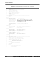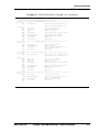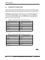
1
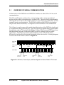
Interfacing the DSP560xx/DSP563xx
Families to the Crystal CS4226
Multichannel Codec
by
Mathew Abraham
Motorola, Incorporated
Semiconductor Products Sector
6501 William Cannon Drive West
Austin, TX 78735-8598
OnCE is a trademark of Motorola, Inc.
© MOTOROLA INC., 1998
Order by this number: APR36/D
Motorola reserves the right to make changes without further notice to any products herein to improve
reliability, function, or design. Motorola does not assume any liability arising out of the application or
use of any product or circuit described herein; neither does it convey any license under its patent rights
nor the rights of others. Motorola products are not designed, intended, or authorized for use as
components in systems intended for surgical implant into the body, or other application in which the
failure of the Motorola product could create a situation where personal injury or death may occur.
Should Buyer purchase or use Motorola products for any such unintended or unauthorized application,
Buyer shall indemnify and hold Motorola and its officers, employees, subsidiaries, affiliates, and
distributors harmless against all claims, costs, damages, and expenses, and reasonable attorney fees
arising out of, directly or indirectly, any claim of personal injury or death associated with such
unintended or unauthorized use, even if such claim alleges that Motorola was negligent regarding the
design or manufacture of the part. Motorola and
are registered trademarks of Motorola, Inc.
Motorola, Inc. is an Equal Opportunity/Affirmative Action Employer.
TABLE OF CONTENTS
INTRODUCTION . . . . . . . . . . . . . . . . . . . . . . . . . . . . . . . . . . . . . . . . . . .
1.1
INTRODUCTION . . . . . . . . . . . . . . . . . . . . . . . . . . . . . . . . . . . .
1.2
SCOPE . . . . . . . . . . . . . . . . . . . . . . . . . . . . . . . . . . . . . . . . . . . .
1.3
THE DSP56XXX IN SURROUND SOUND
APPLICATIONS . . . . . . . . . . . . . . . . . . . . . . . . . . . . . . . . . . . . .
1.4
THE CS4226 IN SURROUND SOUND APPLICATIONS. . . . . .
1-1
1-3
1-3
1-3
1-4
INTERFACE CONSIDERATIONS . . . . . . . . . . . . . . . . . . . . . . . . . . . . . .
2.1
INTERFACE CONSIDERATIONS . . . . . . . . . . . . . . . . . . . . . . .
2.2
COMMUNICATION PINS . . . . . . . . . . . . . . . . . . . . . . . . . . . . . .
2.3
ANALOG AND DIGITAL INPUT/OUTPUT . . . . . . . . . . . . . . . . .
2-1
2-3
2-3
2-4
COMMUNICATIONS PROTOCOL . . . . . . . . . . . . . . . . . . . . . . . . . . . . .
3.1
OVERVIEW OF SERIAL COMMUNICATIONS . . . . . . . . . . . . .
3.2
PROGRAMMING THE SSI FOR I2S . . . . . . . . . . . . . . . . . . . . .
3.3
PROGRAMMING THE SAI FOR I2S . . . . . . . . . . . . . . . . . . . . .
3.4
SERIAL BIT CLOCK AND FRAME SYNC GENERATION. . . . .
3-1
3-3
3-4
3-5
3-6
INTERFACE EXAMPLES . . . . . . . . . . . . . . . . . . . . . . . . . . . . . . . . . . . .
4.1
CDB4226 EVALUATION BOARD TO DSP56009EVM
AND DSP56302EVM . . . . . . . . . . . . . . . . . . . . . . . . . . . . . . . . .
4.2
JUMPER AND SWITCH SETTINGS . . . . . . . . . . . . . . . . . . . . .
4.3
SOFTWARE CONFIGURATION . . . . . . . . . . . . . . . . . . . . . . . .
4.4
HEADER PIN CONNECTIONS . . . . . . . . . . . . . . . . . . . . . . . . .
4-1
4-3
4-3
4-4
4-8
REFERENCE MATERIAL . . . . . . . . . . . . . . . . . . . . . . . . . . . . . . . . . . . . 5-1
5.1
REFERENCES . . . . . . . . . . . . . . . . . . . . . . . . . . . . . . . . . . . . . . 5-3
MOTOROLA
Crystal 4226 Multichannel Codec Interface
iii
iv
Crystal 4226 Multichannel Codec Interface
MOTOROLA
LIST OF FIGURES
Figure 2-1
DSP56302/CS4226 Pin Connections . . . . . . . . . . . . . . . . . . . . . . . . 2-3
Figure 3-1
Bit Clock, Frame Sync, and Data Signals for Stereo Data
in I2S Format. . . . . . . . . . . . . . . . . . . . . . . . . . . . . . . . . . . . . . . . . . . 3-3
Figure 3-2
ESSI0 Control Register A (CRA)
(Located at X:$FFFFB5) . . . . . . . . . . . . . . . . . . . . . . . . . . . . . . . . . . 3-5
Figure 3-3
ESSI0 Control Register B (CRB)
(Located at X:$FFFFB6) . . . . . . . . . . . . . . . . . . . . . . . . . . . . . . . . . . 3-5
Figure 3-4
SAI Receive Control/Status Register (RCS)
(Located at X:$FFE1) . . . . . . . . . . . . . . . . . . . . . . . . . . . . . . . . . . . . 3-6
Figure 3-5
SAI Transmit Control/Status Register (TCS)
(Located at X:$FFE4) . . . . . . . . . . . . . . . . . . . . . . . . . . . . . . . . . . . . 3-6
Figure 3-6
PLL Control Register (PCTL)
(Located at X:$FFFFFD) . . . . . . . . . . . . . . . . . . . . . . . . . . . . . . . . . . 3-8
MOTOROLA
Crystal 4226 Multichannel Codec Interface
v
vi
Crystal 4226 Multichannel Codec Interface
MOTOROLA
LIST OF TABLES
Table 4-1
Jumper Settings on CDB4226 . . . . . . . . . . . . . . . . . . . . . . . . . . . . . . 4-3
Table 4-2
Switch Settings on CDB4226 . . . . . . . . . . . . . . . . . . . . . . . . . . . . . . 4-3
Table 4-3
CDB4226/DSP56302EVM Header Connections . . . . . . . . . . . . . . . 4-8
Table 4-4
CDB4226 to DSP56009EVM Header Connections . . . . . . . . . . . . . . 4-8
MOTOROLA
Crystal 4226 Multichannel Codec Interface
vii
viii
Crystal 4226 Multichannel Codec Interface
MOTOROLA
LIST OF EXAMPLES
Example 4-1
Batch File To Initialize CDB4226 . . . . . . . . . . . . . . . . . . . . . . . . . . . 4-4
Example 4-2
DSP56302EVM Pass-Through Code . . . . . . . . . . . . . . . . . . . . . . . . 4-5
MOTOROLA
Crystal 4226 Multichannel Codec Interface
ix
x
Crystal 4226 Multichannel Codec Interface
MOTOROLA
SECTION 1
INTRODUCTION
Introduction
1.1
1.2
1.3
1.4
1-2
INTRODUCTION. . . . . . . . . . . . . . . . . . . . . . . . . . . . . . . . . . . . . 1-3
SCOPE . . . . . . . . . . . . . . . . . . . . . . . . . . . . . . . . . . . . . . . . . . . . 1-3
THE DSP56XXX IN SURROUND SOUND
APPLICATIONS . . . . . . . . . . . . . . . . . . . . . . . . . . . . . . . . . . . . . 1-3
THE CS4226 IN SURROUND SOUND APPLICATIONS . . . . . . 1-4
Crystal 4226 Multichannel Codec Interface
MOTOROLA
Introduction
Introduction
1.1
INTRODUCTION
A common application of Motorola’s DSP560xx and DSP563xx Digital Signal Processors
(DSPs) is professional and consumer-level audio processing. These DSPs are a popular
choice in products ranging from recording studio effects processors to home theater
surround sound decoders.
1.2
SCOPE
This article focuses primarily on the DSP56xxx as a surround sound decoder and on the
accompanying hardware a surround sound application requires.
1.3
THE DSP56XXX IN SURROUND SOUND APPLICATIONS
Minimally, digital surround sound processing requires three components:
surround-encoded source material, a software-based or hardware-based decoding
solution, and multiple Digital-To-Analog (D/A) converters to supply the analog
multichannel output.
Source material that has digitally encoded surround sound can be in the form of
LaserDiscs or Digital Versatile Disks (DVDs), which typically contain Dolby Pro-Logic,
Dolby Digital, or Digital Feeder System (DTS) encoded soundtracks. Decoding this
material in real-time from a bit-stream to multichannel digital audio requires a
hardware-based solution such as the DSP56009 or DSP56362. The final component in
surround sound processing converts the multichannel digital audio to multichannel
analog audio.
Traditionally, the surround sound process employed multiple mono or stereo D/A
converters to provide the number of analog outputs needed. Replacing these multiple
codecs with a single integrated multichannel codec, such as the CS4226 from Crystal
Semiconductor, Inc., would simplify the design as well as reduce cost.
MOTOROLA
Crystal 4226 Multichannel Codec Interface
1-3
Introduction
The CS4226 in Surround Sound Applications
1.4
THE CS4226 IN SURROUND SOUND APPLICATIONS
The CS4226 contains one stereo Analog-to-Digital (A/D) converter, one mono A/D
converter, and six D/A converters on a single chip. All converters have 20-bit resolution
and programmable input gain and output attenuation. The CS4226 will also accept and
transmit Sony/Phillips Digital Interface (S/PDIF) digital data signals. These features
make this particular codec attractive for home theater applications.
A common scenario is to use the S/PDIF receiver on the CS4226 to pass an encoded
audio bitstream to the DSP. The DSP will decode the bitstream into its constituent
channels and perform any desired post-processing. For Dolby Digital or DTS bitstreams,
the output of the decoder is typically six channels of digital audio, more commonly
referred to as “5.1” channels. The six-channel D/A converters on the CS4226 can convert
the six individual data streams into six analog outputs. This solution replaces a
multiple-chip A/D and D/A configuration with a single chip for surround sound
applications.
1-4
Crystal 4226 Multichannel Codec Interface
MOTOROLA
SECTION 2
INTERFACE CONSIDERATIONS
Interface Considerations
2.1
2.2
2.3
2-2
INTERFACE CONSIDERATIONS . . . . . . . . . . . . . . . . . . . . . . . 2-3
COMMUNICATION PINS . . . . . . . . . . . . . . . . . . . . . . . . . . . . . . 2-3
ANALOG AND DIGITAL INPUT / OUTPUT . . . . . . . . . . . . . . . . 2-4
Crystal 4226 Multichannel Codec Interface
MOTOROLA
Interface Considerations
Interface Considerations
2.1
INTERFACE CONSIDERATIONS
The Motorola DSP56000 family and the Crystal CS4226 can be interfaced without glue
logic. Because these parts are designed with similar communication protocols in mind,
configuration is a trivial issue. Detailed connection circuitry, including capacitors and
pull-up resistors, will not be discussed here. Please refer to each part’s respective data
sheet for assistance in designing appropriate interface circuitry.
2.2
COMMUNICATION PINS
The Crystal CS4226 codec is able to communicate with the Motorola DSP560xx or
DSP563xx families via a serial interface. Depending on which DSP chip derivative is
used, the serial interface may be a Synchronous Serial Interface (SSI) or a Serial Audio
Interface (SAI). The DSP563xx derivatives use an Enhanced SSI (ESSI) that includes up
to three transmitters, which can be programmed to transmit three stereo channels or six
total channels.
The ESSI facilitates the implementation of surround sound decoding because six
channels can be transmitted in parallel, removing the need for multiplexing the outputs.
Refer to Figure 2-1 for signal connections between the DSP56302 ESSI and the CS4226
codec.
DSP56302
CS4226
(master)
(slave)
SCK0
SCLK
Coaxial S/PDIF
Receive/Transmit
RX1
ESSI0
Digital audio
bitstream
SC02
LRCK
SRD0
SDOUT1
STD0
SC00
SC01
SDIN1
SDIN2
SDIN3
RX2
Optical S/PDIF
Receive/Transmit
AIN
AOUT
3
Analog in
6
Analog out
Figure 2-1 DSP56302 / CS4226 Pin Connections
MOTOROLA
Crystal 4226 Multichannel Codec Interface
2-3
Interface Considerations
Analog and Digital Input/Output
2.3
ANALOG AND DIGITAL INPUT/OUTPUT
The CS4226 handles audio information with both analog and digital Input/Output
(I/O). It can support up to three simultaneous analog input channels or one digital
input channel. The carrier format of the resulting data, either directly from the digital
input, or after A/D conversion of the analog channels, can be configured to be Inter
Integrated-Circuit Sound (I2S). I2S is an industry standard format for the transfer of
Pulse Code Modulation (PCM) digital audio and will be discussed in the next section.
Encoded multichannel digital bitstreams such as AC-3 or MPEG can be input through a
coaxial interface or optical S/PDIF from a LaserDisc or DVD player. The CS4226 can be
programmed to notify the user of the presence of certain bitstreams, since it has built-in
detection of AC-3 and MPEG. These bitstreams are passed to the DSP, which decodes
them into discrete linear PCM channels and performs any desired processing. The PCM
bitstreams are passed back to the CS4226 and can be converted to analog or output
digitally via coaxial interface or optical S/PDIF.
2-4
Crystal 4226 Multichannel Codec Interface
MOTOROLA
SECTION 3
COMMUNICATIONS PROTOCOL
Communications Protocol
3.1
3.2
3.3
3.4
3-2
OVERVIEW OF SERIAL COMMUNICATIONS . . . . . . . . . . . . . 3-3
PROGRAMMING THE SSI FOR I2S. . . . . . . . . . . . . . . . . . . . . . 3-4
PROGRAMMING THE SAI FOR I2S. . . . . . . . . . . . . . . . . . . . . . 3-5
SERIAL BIT CLOCK AND FRAME SYNC GENERATION . . . . . 3-6
Crystal 4226 Multichannel Codec Interface
MOTOROLA
Communications Protocol
Overview of Serial Communications
3.1
OVERVIEW OF SERIAL COMMUNICATIONS
All derivatives of the DSP560xx and DSP563xx families use either SSI or SAI for serial
communications.
The SSI is a full-duplex serial port for communicating with a variety of peripheral
devices such as codecs, microprocessors, or other DSPs. The port is fully programmable,
allowing the user to choose the number of bits per word, the protocol, the clock, and the
transmit/receive synchronization. The ESSI is available on the DSP563xx derivatives
and provides three transmitters, as compared to one transmitter on the standard SSI.
The SAI port is used in many of the audio-based derivatives of the DSP560xx family and
is an important subset of the SSI port. The SAI supports by default many popular audio
data formats, such as I2S developed by Philips, Compact Disk Protocol (CDP) from Sony,
and Matsushita Electronic Corporation (MEC) protocol, making it ideal for audio
applications. The I2S format and its implementation on the SAI and SSI will be
discussed to help facilitate the interface examples in the next section. A timing diagram
of stereo data in I2S format is shown in Figure 3-1.
Serial Bit
Clock
Frame Sync
Clock
Left Word
Frame
Right Word
Frame
Serial Data
LSB of last
Right Word
MSB of Left
Word
LSB of Left
Word
MSB of
Right Word
LSB of Right
Word
Figure 3-1 Bit Clock, Frame Sync, and Data Signals for Stereo Data in I2S Format
MOTOROLA
Crystal 4226 Multichannel Codec Interface
3-3
Communications Protocol
Programming the SSI for I2S
The I2S format requires a bit clock, a frame clock, and a data line. For stereo data, each
frame cycle must contain a left word and a right word. The left word is aligned with the
low level and the right word with the high level of a frame cycle. The number of bits per
word varies depending on the number of bit clock periods contained within one frame
pulse. As shown in Figure 3-1, the words are aligned in such a way that the first bit of a
left or right word occurs one bit clock cycle after the onset of the frame pulse (frame
pulse = 1/2 frame period). The SSI and the SAI ports can be configured to handle the I2S
carrier format essentially by programming their respective control registers. The
important portions of the control registers that pertain to I2S are discussed below. Refer
to the respective parts’ user’s manual to correctly program the remaining bits in the
control words.
3.2
PROGRAMMING THE SSI FOR I2S
The SSI port is more flexible than the SAI port and thus requires more programming to
define a particular data format such as I2S. The example used in this section will focus
on the DSP56302 ESSI port, which has two control registers, Control Register A (CRA)
and Control Register B (CRB), shown in Figure 3-2 and Figure 3-3. These registers
define how the SSI handles data.
CRA defines the timing of the necessary signals; PM[7:0] (Bits 0–7) defines the serial bit
clock rate; DC[4:0] (Bits 12–16) gives the number of time slots, or words per frame; and
WL[2:0] (Bits 19–21) defines the number of bits per word. The following equations show
how these bits define the clocking signals:
Serial Bit Clock
=
Frame Sync Clock
=
DSPCoreClock
-------------------------------------------2 × ( PM + 1 )
SerialBitClock
-----------------------------------------WL × ( DC + 1 )
Equation 3.1
Equation 3.2
For example, if the DSP Core Clock = 64.512 MHz, PM = 13, WL = 24, and DC = 1:
Serial Bit Clock
=
Frame Sync Clock =
3-4
64.512MHz
------------------------------- = 2.304MHz
2 × ( 13 + 1 )
2.304MHz
------------------------------- = 48.000kHz
24 × ( 1 + 1 )
Equation 3.3
Equation 3.4
Crystal 4226 Multichannel Codec Interface
MOTOROLA
Communications Protocol
Programming the SAI for I2S
11
10
9
8
PSR
23
7
6
5
4
3
2
1
0
PM7
PM6
PM5
PM4
PM3
PM2
PM1
PM0
17
16
15
14
13
12
DC4
DC3
DC2
DC1
DC0
22
21
20
19
18
SSC1
WL2
WL1
WL0
ALC
Figure 3-2 ESSI Control Register A (CRA) (Located at X:$FFFFB5)
11
10
9
8
7
6
5
4
3
2
1
0
CKP
FSP
FSR
FSL1
FSL0
SHFD
SCKD
SCD2
SCD1
SCD0
OF1
OF0
23
22
21
20
19
18
17
16
15
14
13
12
REIE
TEIE
RLIE
TLIE
RIE
TIE
RE
TE0
TE1
TE2
MOD
SYN
Figure 3-3 ESSI Control Register B (CRB) (Located at X:$FFFFB6)
CRB defines the functionality of the port; FSL[1:0] (Bits 7-8) defines the shape of the
frame pulse; FSR (Bit 9) chooses word alignment; FSP (Bit 10) defines the frame sync
polarity; CKP (Bit 11) defines the bit clock polarity; SYN (Bit 12) chooses between
asynchronous/synchronous transmit and receive; and MOD (Bit 13) chooses Normal
mode or Network mode.
To conform to I2S standards, the frame pulse should be one word long. The first word bit
should lag the frame pulse by one serial clock, as shown in Figure 3-1. The frame sync
and bit clock should clock in data on the falling edge, choose synchronous mode for
simplicity, and (for stereo data) choose Network mode to allow for two words per frame.
3.3
PROGRAMMING THE SAI FOR I2S
The SAI port is more readily configurable for handling I2S than is the SSI port. It
defaults to two words per frame, which simplifies much of the configuration. The Baud
Rate Control (BRC) register, the Receive Control/Status (RCS) register, and the Transmit
Control/Status (TCS) register dictate the behavior of the SAI port.
The BRC register determines the serial bit clock rate, similar to the PM[7:0] bits in the
ESSI CRA. The Receive and Transmit Control registers, shown in Figure 3-4 and
Figure 3-5, are identical in defining the data format. Bits 4 and 5 determine the word
MOTOROLA
Crystal 4226 Multichannel Codec Interface
3-5
Communications Protocol
Serial Bit Clock and Frame Sync Generation
length. Bit 7 chooses the frame sync polarity, and Bit 8 chooses the bit clock polarity. Bit
9 defines the word alignment.
11
10
9
8
7
6
5
4
3
RXIE
RDWT
RREL
RCKP
RLRS
RDIR
RWL1
RWL0
RMST
2
23
22
21
20
19
18
17
16
15
14
RRDF
RLDF
1
0
R1EN
R0EN
13
12
RXIL
Figure 3-4 SAI Receive Control/Status Register (RCS) (Located at X:$FFE1)
11
10
9
8
7
6
5
4
3
2
1
0
TXIE
TDWE
TREL
TCKP
TLRS
TDIR
TWL1
TWL0
TMST
T2EN
T1EN
T0EN
23
22
21
20
19
18
17
16
15
14
13
12
TRDE
TLDE
TXIL
Figure 3-5 SAI Transmit Control/Status Register (TCS) (Located at X:$FFE4)
3.4
SERIAL BIT CLOCK AND FRAME SYNC GENERATION
An important step in correctly implementing I2S is defining the appropriate bit clock
and frame sync frequencies. In this discussion, the DSP is the master device and
therefore supplies the necessary clocks to the CS4226 codec. The codec uses the frame
sync clock as its Analog-to-Digital (A/D) sampling frequency and uses the bit clock to
synchronize communication with the DSP. In order to choose a 44.1 kHz or a 48 kHz
sampling frequency (Fs) for the codec, careful consideration must be given to the
generation of these clocks in the DSP. Once an Fs is chosen (say 48 kHz) the Phase Lock
Loop (PLL) on the DSP must be programmed to provide an exact multiple of the chosen
frequency.
In the example given in Equation 3.3 and Equation 3.4, the PLL was programmed to
create a DSP core frequency of 64.512 MHz, which is exactly 1344*48 kHz. The
DSP56302 PLL Control Register (PCTL) can be configured to provide almost any
desired serial clock frequency by adjusting the DSP core clock frequency. This is
accomplished by modifying the external crystal frequency (Fext) with multiply and
divide bits in the PCTL, shown in Figure 3-6. MF[11:0] (Bits 0-11) applies a
multiplication factor to Fext, and PD[3:0] (Bits 20–23) and DF[2:0] (Bits 12–14) are
predivider factor and divider factor bits respectively. Care must be taken to ensure that
at any step the multiplication or division factors do not set the VCO frequency outside
3-6
Crystal 4226 Multichannel Codec Interface
MOTOROLA
Communications Protocol
Serial Bit Clock and Frame Sync Generation
the operating specs of the part. The resulting DSP core clock frequency is shown in
Equation 3.5. Please refer to the appropriate DSP Family Manual for further details on
programming the PLL.
DSP Core Clock =
F ext × ( MF + 1 )
----------------------------------------DF
( PD + 1 ) × 2
Equation 3.5
For example, if the external crystal = 24.576 MHz, MF = 20, PD = 7, and DF = 0, then:
DSP Core Clock =
24.576 × ( 20 + 1 )
--------------------------------------------- = 64.512MHz
0
(7 + 1) × 2
11
10
9
8
7
6
5
4
3
2
1
0
MF11
MF10
MF9
MF8
MF7
MF6
MF5
MF4
MF3
MF2
MF1
MF0
Equation 3.6
23
22
21
20
19
18
17
16
15
14
13
12
PD3
PD2
PD1
PD0
COD
PEN
PSTP
XTLD
XTLR
DF2
DF1
DF0
Figure 3-6 PLL Control Register (PCTL) (Located at X:$FFFFFD)
MOTOROLA
Crystal 4226 Multichannel Codec Interface
3-7
Communications Protocol
Serial Bit Clock and Frame Sync Generation
3-8
Crystal 4226 Multichannel Codec Interface
MOTOROLA
SECTION 4
INTERFACE EXAMPLES
Interface Examples
4.1
4.2
4.3
4.4
4-2
CDB4226 EVALUATION BOARD TO DSP56009EVM
AND DSP56302EVM . . . . . . . . . . . . . . . . . . . . . . . . . . . . . . . . . 4-3
JUMPER AND SWITCH SETTINGS. . . . . . . . . . . . . . . . . . . . . . 4-3
SOFTWARE CONFIGURATION. . . . . . . . . . . . . . . . . . . . . . . . . 4-4
HEADER PIN CONNECTIONS. . . . . . . . . . . . . . . . . . . . . . . . . . 4-8
Crystal 4226 Multichannel Codec Interface
MOTOROLA
Interface Examples
CDB4226 Evaluation Board to DSP56009EVM and DSP56302EVM
4.1
CDB4226 EVALUATION BOARD TO DSP56009EVM
AND DSP56302EVM
This section illustrates the interface topics with development boards provided by
Motorola and Crystal Semiconductor.
4.2
JUMPER AND SWITCH SETTINGS
The Crystal CDB4226 Evaluation Board provides seven shared analog inputs (any three
active at once), six discrete analog outputs, optical and coaxial S/PDIF receive and
transmit, and serial interfaces through DSP and auxiliary ports. The CDB4226 can be
configured to act as a slave device to the DSP with a combination of switch, jumper, and
control byte settings. The switch and jumper settings are given in Table 4-1 and
Table 4-2. Please refer to the Crystal CDB4226 Product Information document for
details on these settings.
Table 4-1 Jumper Settings on CDB4226
Jumper(s)
Position
XT_SEL
XTAL
HDR1-7
AIN
RX_SEL
RX2 (for optical S/PDIF input) open (for coaxial S/PDIF input)
Table 4-2 Switch Settings on CDB4226
#
MOTOROLA
SW1
SW2
1
On
Off
2
Off
Off
3
Off
Off
4
On
On
5
On
Off
6
On
—
Crystal 4226 Multichannel Codec Interface
4-3
Interface Examples
Software Configuration
4.3
SOFTWARE CONFIGURATION
The Crystal CDB4226 requires certain control registers to be initialized to operate in the
desired mode. A DOS-executable provided by Crystal called WRSPI.EXE uses a host
computer to initialize the control bytes. The batch file listing shown in Example 4-1
gives the necessary commands to set up the CDB4226 as the slave device using I2S data
format. Please refer to the Crystal CS4226 Product Information document to customize
the initialization of these control bytes.
Example 4-1 Batch File To Initialize CDB4226
rem RSTSPI.EXE sends a soft reset to the CDB4226
rstspi
rem Begin initialization
rem Clock Mode Byte: PLL driven by coaxial S/PDIF in, XT=256Fs, CLKOUT=256Fs
wrspi 01 04 -p00
rem Converter Control Byte
wrspi 02 00
rem DAC Control Byte
wrspi 03 00
rem Output Attenuator Bytes: no attenuation
wrspi 04 00
wrspi 05 00
wrspi 06 00
wrspi 07 00
wrspi 08 00
wrspi 09 00
rem ADC Control Byte: S/PDIF input to SDOUT1
wrspi 0b 40
rem Input Control Byte
wrspi 0c 00
rem DSP Port Mode Byte: I2S data, falling edge, DSP is slave, 64 bit clocks/Fs period
wrspi 0e ec
rem Auxiliary Port Mode Byte
wrspi 0f 00
rem Auxiliary Port Control Byte
wrspi 10 00
4-4
Crystal 4226 Multichannel Codec Interface
MOTOROLA
Interface Examples
Software Configuration
The DSP control registers are initialized and set into Master mode with a pass-through
program, which takes data in from the ESSI receive pin and returns immediately to the
ESSI transmit pin. An example of pass-through code written specifically for the
DSP56302EVM is shown in Example 4-2 with the control register initializations shown
in bold. The pass-through program is a simple example illustrating how the control
registers are updated; any program can incorporate the code in bold to initialize the
control registers. The code can be downloaded and run on the DSP using the EVM56302
Debugger from Domain Technologies, Inc.
Example 4-2 DSP56302EVM Pass-Through Code
;***************************************************************************
; 4226PASS.ASM
;
; Multi-channel pass thru for the DSP56302EVM using the
; Crystal CS4226 Codec.
;
; Based on DSP303EVM passthru code, modified by Mathew Abraham
; July 1997
;***************************************************************************
nolist
include 'ioequ.asm'
include 'intequ.asm'
include 'vectors.asm'
list
;***************************************************************************
;---Buffer for talking to the CS4226
org x:$0
RX_BUFF_BASE equ *
RX_data_1_2 ds 1
;data time slot
RX_data_3_4 ds 1
;data time slot
TX_BUFF_BASE equ *
TX_data_1_2 ds 1
;data time slot
TX_data_3_4 ds 1
;data time slot
RX_PTR
ds 1
;Pointer for rx
TX_PTR
ds 1
;Pointer for tx
1/2 for RX ISR
3/4 for RX ISR
1/2 for TX ISR
3/4 for TX ISR
buffer
buffer
org p:$100
START
main
movep#$740014,x:M_PCTL
movep#$012421,x:M_BCR
ori #3,mr
movec#0,sp
move #0,omr
move #$40,r6
move #-1,m6
jsr ada_init
;PLL=24.576*((20+1)/(7+1))=64.512 MHz (64.512MHz/1344=48kHz)
;set up one ext. wait state for all AAR areas
;mask interrupts
;clear hardware stack pointer
;operating mode 0
;initialise stack pointer
;linear addressing
;initialize codec
loop_1
jset #2,x:M_SSISR0,*
jclr #2,x:M_SSISR0,*
move x:RX_BUFF_BASE,a
move x:RX_BUFF_BASE+1,b
jsr process_stereo
move a,x:TX_BUFF_BASE
move b,x:TX_BUFF_BASE+1
jmp loop_1
process_stereo
nop
nop
nop
rts
include 'ada_init.asm'
echo
end
MOTOROLA
;wait for frame sync to pass
;wait for frame sync
;receive left
;receive right
;any audio processing happens here
;transmit left
;transmit right
;any audio processing happens here
Crystal 4226 Multichannel Codec Interface
4-5
Interface Examples
Software Configuration
Example 4-2 DSP56302EVM Pass-Through Code (Continued)
;**************************************************************************
;
ADA_INIT.ASM
;
Include for 4226PASS.ASM to initialize the CS4226
;
;
Copyright (c) MOTOROLA 1997
;
Semiconductor Products Sector
;
Digital Signal Processing Division
;
;
History:
;
14 June 1996: RLR/LJD - ver.1.0
;
22 July 1997: MTA
;**************************************************************************
page 132,60
org p:
ada_init
;set up control words for ESSI0
movep#$0000,x:M_PCRC
movep#$18180d,x:M_CRA0
movep#$ff341c,x:M_CRB0
movep#$003F,x:M_PCRC
;reset delay for codec
do #1000,_delay_loop
rep #65
nop
_delay_loop
movep#$000C,x:M_IPRP
andi #$FC,mr
;CLB == 0
jclr #3,x:M_SSISR0,*
jset #3,x:M_SSISR0,*
jclr #3,x:M_SSISR0,*
jset #18,x:RX_BUFF_BASE,*
;CLB == 1
bset #18,x:TX_BUFF_BASE
do #4,_init_loopB
jclr #2,x:M_SSISR0,*
jset #2,x:M_SSISR0,*
_init_loopB
rts
;turn off ESSI0 port
;PM=13 --> SCLK = 64.512MHz/((13+1)*2) = 2.304MHz,
;WL=24 bits, 2 W/F --> 2.304MHz/(24*2) = 48kHz
;network/synchronous mode, all transmitters enabled,
;frame clocked on falling edge
;turn on ESSI0
;1 ms delay (assuming 64.512MHz VCO)
;set interrupt priority level for ESSI0 to 3
;enable interrupts
;wait
;wait
;wait
;loop
until
until
until
until
rx frame bit==1
rx frame bit==0
rx frame bit==1
CLB set
;set CLB
;wait until tx frame bit==1
;wait until tx frame bit==0
;****************************************************************************
;
SSI0_ISR.ASM
Ver.2.0
;
Example program to handle interrupts through
;
the 56302 ESSI0 to move audio through the CS4226
;
;
Copyright (c) MOTOROLA 1995, 1996, 1997
;
Semiconductor Products Sector
;
Digital Signal Processing Division
;
;
upon entry:
;
R6 must be the stack pointer
;
corrupts:
;
R6
;
;
History:
;
14 June 1996: RLR/LJD - ver 1.0
;
22 July 1997: MTA
4-6
Crystal 4226 Multichannel Codec Interface
MOTOROLA
Interface Examples
Software Configuration
Example 4-2 DSP56302EVM Pass-Through Code (Continued)
;*****************************************************************************
;----the actual interrupt service routines (ISRs) follow:
;************************ SSI TRANSMIT ISR *********************************
ssi_txe_isr
bclr
#4,x:M_SSISR0
; Read SSISR to clear exception flag
; explicitly clears underrun flag
ssi_tx_isr
move
r0,x:(r6)+
; Save r0 to the stack.
move
m0,x:(r6)+
; Save m0 to the stack.
move
#1,m0
; Modulus 2 buffer.
move
x:TX_PTR,r0
; Load the pointer to the tx buffer.
nop
movep
x:(r0)+,x:M_TX00
; SSI transfer data register.
move
r0,x:TX_PTR
; Update tx buffer pointer.
move
x:-(r6),m0
; Restore m0.
move
x:-(r6),r0
; Restore r0.
rti
;********************* SSI TRANSMIT LAST SLOT ISR **************************
ssi_txls_isr
move
r0,x:(r6)+
; Save r0 to the stack.
move
#TX_BUFF_BASE,r0
; Reset pointer.
move
r0,x:TX_PTR
; Reset tx buffer pointer just in
; case it was corrupted.
move
x:-(r6),r0
; Restore r0.
rti
;************************** SSI receive ISR ********************************
ssi_rxe_isr
bclr
#5,x:M_SSISR0
; Read SSISR to clear exception flag
; explicitly clears overrun flag
ssi_rx_isr
move
r0,x:(r6)+
; Save r0 to the stack.
move
m0,x:(r6)+
; Save m0 to the stack.
move
#1,m0
; Modulo 2 buffer.
move
x:RX_PTR,r0
; Load the pointer to the rx buffer.
nop
movep
x:M_RX0,x:(r0)+
; Read out received data to buffer.
move
r0,x:RX_PTR
; Update rx buffer pointer.
move
x:-(r6),m0
; Restore m0.
move
x:-(r6),r0
; Restore r0.
rti
;********************** SSI receive last slot ISR **************************
ssi_rxls_isr
move
r0,x:(r6)+
; Save r0 to the stack.
move
#RX_BUFF_BASE,r0
; Reset rx buffer pointer just in
; case it was corrupted.
move
r0,x:RX_PTR
; Update rx buffer pointer.
move
x:-(r6),r0
; Restore r0.
rti
MOTOROLA
Crystal 4226 Multichannel Codec Interface
4-7
Interface Examples
Header Pin Connections
4.4
HEADER PIN CONNECTIONS
Interfacing the Crystal CDB4226 Evaluation Board to a Motorola Evaluation Module
requires connecting the two boards with jumper wires that carry clock and data signals.
Both boards have a header block to make pin-to-pin connections to external devices.
See Figure 2-1 on page 2-3 for an example of the necessary connections between the
DSP56302EVM and the CDB4226. These connections are also listed in Table 4-3.
Connections to the DSP56009EVM are listed in Table 4-4. These examples illustrate
how the Crystal CS4226 multichannel codec can be interfaced to Motorola DSPs to
implement surround sound decoding.
Table 4-3 CDB4226/DSP56302EVM Header Connections
DSP_HDR on CDB4226
SCLK(7*)
LRCK(5)
SDOUT(3)
SDIN1(17)
SDIN2(15)
SDIN3(13)
J7 (ESSI0) on DSP56302EVM
SCK0(2)
SC02(12)
SRD0(8)
STD0(6)
SC00(4)
SC01(10)
* Header pin number
Table 4-4 CDB4226 to DSP56009EVM Header Connections
DSP_HDR on CDB4226
SCLK(7*)
LRCK(5)
SDOUT(3)
SDIN1(17)
SDIN2(15)
SDIN3(13)
J5 on DSP56009EVM
SCKT(15)
WST(13)
SDI0(9)
SDO0(17)
SDO1(19)
SDO2(21)
* Header pin number
4-8
Crystal 4226 Multichannel Codec Interface
MOTOROLA
SECTION 5
REFERENCE MATERIAL
Reference Material
5.1
5-2
REFERENCES . . . . . . . . . . . . . . . . . . . . . . . . . . . . . . . . . . . . . . 5-3
Crystal 4226 Multichannel Codec Interface
MOTOROLA
Reference Material
References
5.1
REFERENCES
For additional information, consult the following documents from Motorola and Crystal
Semiconductor:
DSP56000 Digital Signal Processor Family Manual
DSP56009 Digital Signal Processor User’s Manual
DSP56009EVM User’s Manual
DSP56300 Digital Signal Processor Family Manual
DSP56302 Digital Signal Processor User’s Manual
DSP56302EVM User’s Manual
Crystal CS4226 Preliminary Product Information
Crystal CDB4226 Preliminary Product Information
For a complete list of accessible Motorola DSP documents visit the Motorola website,
reached at the following address:
http://www.motorola-dsp.com/documentation
The example code presented in this application report is available via the Motorola
website, reached at the following address:
http://www.motorola-dsp.com/documentation/appnotes
MOTOROLA
Crystal 4226 Multichannel Codec Interface
5-3
Reference Material
References
5-4
Crystal 4226 Multichannel Codec Interface
MOTOROLA