1
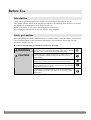
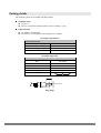
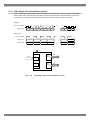
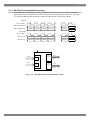
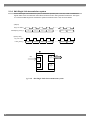
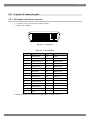
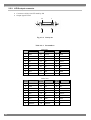
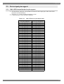
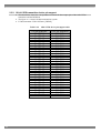
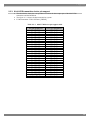
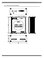
Interface Conversion Adaptor (DVI to LVDS)
IA-573-A
User’s Manual
Ver.1.02
Interface Conversion Adaptor
(DVI to LVDS)
IA-573-A
User’s Manual
2007.2
Ver.1.02
ASTRODESIGN,Inc
Contents
Contents ....................................................................................................................................................................... i
Before Use .................................................................................................................................................................. ii
Introduction.................................................................................................................................................................. ii
Safety precautions....................................................................................................................................................... ii
Packing details ............................................................................................................................................................iii
1. Concerning the IA-573-A................................................................................................................................................. 1
1.1.
1.2.
1.3.
Outline............................................................................................................................................................... 1
Features ............................................................................................................................................................ 1
Parts and their functions.................................................................................................................................... 2
1.3.1.
IA-573-A front panel ............................................................................................................................ 2
1.3.2.
IA-573-A rear panel............................................................................................................................. 3
2. Appendix ......................................................................................................................................................................... 5
2.1.
Manner of data transmission ............................................................................................................................. 5
2.1.1.
12bit Dual Link transmission system................................................................................................... 5
2.1.2.
12bit Single Link transmission system ................................................................................................ 6
2.1.3.
8bit Dual Link transmission system..................................................................................................... 7
2.1.4.
8bit Single Link transmission system .................................................................................................. 8
2.2. Layout of connector pin ..................................................................................................................................... 9
2.2.1.
DVI digital serial input connector......................................................................................................... 9
2.2.2.
LVDS output connector ..................................................................................................................... 10
2.3. Device input pin support.................................................................................................................................. 11
2.3.1.
12bit LVDS transmitter device pin support ........................................................................................ 11
2.3.2.
10 bit LVDS transmitter device pin support ....................................................................................... 12
2.3.3.
8 bit LVDS transmitter device pin support ......................................................................................... 13
2.4. IA-573-A specifications.................................................................................................................................... 14
2.4.1.
Specifications .................................................................................................................................... 14
2.4.2.
Ratings.............................................................................................................................................. 14
2.4.3.
Dimensional outline drawing ............................................................................................................. 15
i
Before Use
Introduction
Thank you for purchasing this DVI-to-LVDS conversion adapter (hereafter IA-573-A).
This manual contains details on the operation procedures to be followed when the IA-573-A is used,
the checkpoints and precautions to be observed, and so on.
Before using the IA-573-A, please read through these instructions.
After reading the manual, keep it in a safe place for future reference.
Safety precautions
Improper handling may lead to malfunctioning or accidents. Before using this adapter, be absolutely
sure to read through the safety precautions listed below: they will help to ensure that you will
operate the adapter correctly.
Observe the following precautions to ensure safe operation.
WARNING
Do not spill liquids inside the adapter or drop inflammable objects
or metal parts into it. Operating the adapter under these conditions
may cause a fire, electric shocks and/or malfunctioning.
CAUTION
Install the adapter in a stable location. Do not stand it on its side.
Rises in temperature caused by heat generation may result in
malfunctioning.
Do not subject the adapter to impact. Doing so may result in
malfunctioning. Take sufficient care when moving the adapter.
When accuracy is a priority, leave the adapter for about 10 to 15
minutes after turning on its power, and wait until its operation has
stabilized before starting to use it.
In the unlikely event that trouble has occurred, disconnect the
adapter's cables, and contact your dealer or an Astrodesign sales
representative.
ii
Packing details
The following items are included with this product.
Standard items
IA-573-A
IA-573-A instruction manual (what you are reading): 1 copy
Optional items
AC adapter, SSA0515A9
The IA-573-A is designed to run using this AC adapter.
AC adapter specifications
S-8453 specifications
Rated output voltage (V)
5
Rated output current (A)
2
Input voltage (VAC)
100 to 240 (rating: 100)
Input power line frequency (Hz)
47 to 63 (rating: 50/60)
AC adapter plug shape
Plug shape
EIAJ
RC-5320A
Voltage classification
2
Outside diameter D1
4.0
Inside diameter D2
1.7
Length (L)
9.5
Polarity display symbol
-
+
L
Inside diameter D2
Outside diameter D1
Plug shape
iii
iv
1
Concerning the IA-573-A
1.1. Outline
The IA-573-A converts DVI-D inputs into LVDS and outputs them.
1.2. Features
Dot clock frequency in wide band
Table 1-2-1 shows the frequency specifications of the input and output dot clocks.
Table 1-2-1
Operation mode
8bit
10bit
SINGLE LINK
Frequency specifications
DVI input (MHz)
LVDS output (MHz)
25 to 135MHz
Interleave mode
ON
12.5 to 82.5 (Transmission rate: 25 to 135MHz)
Interleave mode
OFF
25 to 135MHz
* DVI cable: When a 2-meter cable made by Molex is used
1
Chapter 2
1.3. Parts and their functions
1.3.1. IA-573-A front panel
⑥
② ③ ④ ⑤
①
Fig. 1-3-1
1
2
3
4
5
6
Input connector (DVI connector, Manner of transmission: TMDS)
Interleave mode selector switch: For selecting the interleave mode from ON and OFF
DC jack
LED: Lights when the power is on.
Power switch
Frame ground (FG): Connect here to share the frame ground of the equipment which is
connected to the IA-573-A.
CAUTION
2
Front panel
Always use the power switch to turn the power ON or OFF. Turning the power ON or OFF
by connecting or disconnecting the cable may damage the adapter.
1 Concerning the IA-573-A
1.3.2. IA-573-A rear panel
①
②
Fig. 1-3-2 Rear panel
1
2
Output connector 1 (DFP connector, Manner of transmission: LVDS)
Output connector 2 (DFP connector, Manner of transmission: LVDS)
3
4
2
Appendix
2.1. Manner of data transmission
The data will be transmitted using the interleave mode ON/OFF.
2.1.1. 12bit Dual Link transmission system
For the 12bit Dual Link transmission system, 5 TMDS lines (for data) and 1 CLK line, a total of 6 differential
signals will be used. The interleave mode switch should be set OFF during the data transmission. The Figure
2-1-1 shows the 12bit Dual Link transmission system at resolution 1024 x 768, dot clock 75MHz.
①IN(DVI)
RX_CLK 75MHz
・・・・・・・
RX_DATA_A
D0[11..4]
D1[11..4]
D2[11..4]
D3[11..4]
・・・・・・・
D1022[11..4]
D1023[11..4]
RX_DATA_B
D0[3..0]
D1[3..0]
D2[3..0]
D3[3..0]
・・・・・・・
D1022[3..0]
D1023[3..0]
②OUT(LVDS)
・・・・・・・
TX_CLK 75MHz
TX_DATA_A
D0[11..4]
D1[11..4]
D2[11..4]
D3[11..4]
・・・・・・・
D1022[11..4]
D1023[11..4]
TX_DATA_B
D0[3..0]
D1[3..0]
D2[3..0]
D3[3..0]
・・・・・・・
D1022[3..0]
D1023[3..0]
IA
8bit
4bit
Fig. 2-1-1
DVI
Receiver
A
DVI
Receiver
B
LVDS
connector
A
LVDS
connector
B
8bit
CH1
4bit
CH2
12bit Dual Link data transmission system
5
2.1.2. 12bit Single Link transmission system
For the 12bit Single Link transmission system, 2 TMDS lines (for data) and 1 CLK line, a total of 3 differential
signals will be used. The interleave mode switch should be set ON during the data transmission. The Figure
2-1-2 shows the 12bit Single Link transmission system at resolution 1024 x 768, dot clock 75MHz.
①IN(DVI)
RX_CLK 150MHz
RX_DATA_A
・・・・・・・
D0
[11..4]
D0
[3..0]
D1
[11..4]
D1
[3..0]
D2
[11..4]
D2
[3..0]
D3
[11..4]
D3
[3..0]
・・・・・・・
D1022 D1022 D1023 D1023
[11..4] [3..0] [11..4] [3..0]
②OUT(LVDS)
TX_CLK 75MHz
・・・・・・・
TX_DATA_A
D0[11..4]
D1[11..4]
D2[11..4]
D3[11..4]
・・・・・・・
D1022[11..4]
D1023[11..4]
TX_DATA_B
D0[3..0]
D1[3..0]
D2[3..0]
D3[3..0]
・・・・・・・
D1022[3..0]
D1023[3..0]
IA
12bit
DVI
Receiver
A
DVI
Receiver
B
Fig. 2-1-2
6
LVDS
connector
A
LVDS
connector
B
8bit
CH1
4bit
CH2
12bit Single Link data transmission system
2 Appendix
2.1.3. 8bit Dual Link transmission system
For the 8bit Dual Link transmission system, 5 TMDS lines (for data) and 1 CLK line, a total of 6 differential
signals will be used. The interleave mode switch should be set OFF during the data transmission. The Figure
2-1-3 shows the 8bit Dual Link transmission system at resolution 1024 x 768, dot clock 75MHz.
①IN(DVI)
RX_CLK 75MHz
・・・・・・・
LINK #0(DVI_DATA_A)
D0[7..0]
D2[7..0]
D4[7..0]
D6[7..0]
・・・・・・・
D1020[7..0]
D1022[7..0]
LINK #1(DVI_DATA_B)
D1[7..0]
D3[7..0]
D5[7..0]
D7[7..0]
・・・・・・・
D1021[7..0]
D1023[7..0]
②OUT(LVDS)
TX_CLK 75MHz
・・・・・・・
LVDS_DATA_A
D0[7..0]
D2[7..0]
D4[7..0]
D6[7..0]
・・・・・・・
D1020[7..0]
D1022[7..0]
LVDS_DATA_B
D1[7..0]
D3[7..0]
D5[7..0]
D7[7..0]
・・・・・・・
D1021[7..0]
D1023[7..0]
IA
8bit
8bit
DVI
Receiver
A
DVI
Receiver
B
LVDS
connector
A
LVDS
connector
B
8bit
CH1
8bit
CH2
Fig. 2-1-3
8bit Dual Link data transmission system
7
2.1.4. 8bit Single Link transmission system
For the 8bit Single Link transmission system, 2 TMDS lines (for data) and 1 CLK line, a total of 3 differential
signals will be used. The interleave mode switch should be set OFF during the data transmission. The Figure
2-1-2 shows the 8bit Single Link transmission system at resolution 1024 x 768, dot clock 75MHz.
①IN(DVI)
RX_CLK 75MHz
LINK #0(DVI_DATA_A)
・・・・・・・
D0[7..0]
D1[7..0]
D2[7..0]
D3[7..0]
・・・・・・・
D1022[7..0]
D1023[7..0]
D1022[7..0]
D1023[7..0]
②OUT(LVDS)
TX_CLK 75MHz
LVDS_DATA_A
・・・・・・・
D0[7..0]
D1[7..0]
D2[7..0]
D3[7..0]
・・・・・・・
IA
8bit
DVI
Receiver
A
DVI
Receiver
B
ig. 2-1-4
8
LVDS
connector
A
8bit
CH1
LVDS
connector
B
8bit Single Link data transmission system
2 Appendix
2.2. Layout of connector pin
2.2.1. DVI digital serial input connector
•
•
Connector: DVI-I (74320-1004) made by Molex
Input signal : TMDS
1
8 C1
9
16
17
24 C3
Fig. 2-2-1
Table 2-2-1
C2
C5
C4
Pin layout
Pin numbers
Pin No
Signal
Pin No
Signal
1
TMDS DATA2−
16
SENSE
2
TMDS DATA2+
17
TMDS DATA0−
3
TMDS DATA2/4 G
18
TMDS DATA0+
4
TMDS DATA4−
19
TMDS DATA0-5 G
5
TMDS DATA4+
20
TMDS DATA5−
6
DDC CLK
21
TMDS DATA5+
7
DDC DATA
22
TMDS CLK G
8
―
23
TMDS CLK+
9
TMDS DATA1−
24
TMDS CLK−
10
TMDS DATA1+
C1
―
11
TMDS DATA1/3 G
C2
―
12
TMDS DATA3−
C3
―
13
TMDS DATA3+
C4
―
14
+5V
C5
―
15
GND
―
―
* TMDS DATA 0 to 2 for LINK #0, TMDS DATA 3 to 5 for LINK #1
9
2.2.2. LVDS output connector
•
•
Connector: 10226-1210-VE made by 3M
Output signal: LVDS
13
1
26
14
Fig. 2-2-2
Table 2-2-2
Pin layout
Pin numbers
LVDS 1CH
Pin.No
In/Out Signal
入出力信号
Pin.No
In/Out Signal
入出力信号
Pin.No
In/Out Signal
入出力信号
1
GND
10
TCLKG
19
TCG
2
TAG
11
+5V
20
TE-
3
SENS
12
TD-
21
TE+
4
TB-
13
TD+
22
TCLK-
5
TB+
14
TA-
23
TCLK+
6
TC-
15
TA+
24
NC
7
TC+
16
GND
25
TDG
8
TEG
17
TBG
26
GND
9
DDCSCL
18
DDCSDA
―
―
LVDS 2CH
Pin.No
10
In/Out Signal
入出力信号
Pin.No
In/Out Signal
入出力信号
Pin.No
In/Out
Signal
入出力信号
1
GND
10
TCLKG
19
TCG
2
TAG
11
+5V
20
TE-
3
SENS
12
TD-
21
TE+
4
TB-
13
TD+
22
TCLK-
5
TB+
14
TA-
23
TCLK+
6
TC-
15
TA+
24
NC
7
TC+
16
GND
25
TDG
8
TEG
17
TBG
26
GND
9
DDCSCL
18
DDCSDA
―
―
2 Appendix
2.3. Device input pin support
2.3.1. 12bit LVDS transmitter device pin support
•
•
•
The table below shows the correspondence between the data output pins of the 12bit LVDS
transmitter and the RGB data.
The figure 2-3-1 shows the data transmission system
LVDS transmitter: THC63LVD103 [THINE]
Table 2-3-1
12bit LVDS device pin support table
DVI pin assignment
LVDS pin assignment
R0 (LINK #1)
R1 (LINK #1)
R2 (LINK #1)
R3 (LINK #1)
R0 (LINK #0)
R1 (LINK #0)
R2 (LINK #0)
R3 (LINK #0)
R4 (LINK #0)
R5 (LINK #0)
R6 (LINK #0)
R7 (LINK #0)
G0 (LINK #1)
G1 (LINK #1)
G2 (LINK #1)
G3 (LINK #1)
G0 (LINK #0)
G1 (LINK #0)
G2 (LINK #0)
G3 (LINK #0)
G4 (LINK #0)
G5 (LINK #0)
G6 (LINK #0)
G7 (LINK #0)
B0 (LINK #1)
B1 (LINK #1)
B2 (LINK #1)
B3 (LINK #1)
B0 (LINK #0)
B1 (LINK #0)
B2 (LINK #0)
B3 (LINK #0)
B4 (LINK #0)
B5 (LINK #0)
B6 (LINK #0)
B7 (LINK #0)
HS (LINK #0)
VS (LINK #0)
DISP (LINK #0)
TB0 CH2)
TB1 (CH2)
TA0 (CH2)
TA1 (CH2)
TD0 (CH1)
TD1 (CH1)
TA0( CH1)
TA1 (CH1)
TA2 (CH1)
TA3 (CH1)
TA4 (CH1)
TA5 (CH1)
TB2 (CH2)
TB3 (CH2)
TA2 (CH2)
TA3 (CH2)
TD2 (CH1)
TD3 (CH1)
TA6 (CH1)
TB0 (CH1)
TB1 (CH1)
TB2 (CH1)
TB3 (CH1)
TB4 (CH1)
TB4 (CH2)
TB5 (CH2)
TA4 (CH2)
TA5 (CH2)
TD4 (CH1)
TD5 (CH1)
TB5 (CH1)
TB6 (CH1)
TC0 (CH1)
TC1 (CH1)
TC2 (CH1)
TC3 (CH1)
TC4 (CH1)
TC5 (CH1)
TC6 (CH1)
11
2.3.2. 10 bit LVDS transmitter device pin support
•
•
•
The table below shows the correspondence between the data output pins of the 10bit LVDS
transmitter and the RGB data.
The figure 2-3-1 shows the data transmission system
LVDS transmitter: THC63LVD103 [THINE]
Table 2-3-2
12
10bit LVDS device pin support table
DVI pin assignment
LVDS pin assignment
R0 (LINK #1)
R1 (LINK #1)
R0 (LINK #0)
R1 (LINK #0)
R2 (LINK #0)
R3 (LINK #0)
R4 (LINK #0)
R5 (LINK #0)
R6 (LINK #0)
R7 (LINK #0)
G0 (LINK #1)
G1 (LINK #1)
G0 (LINK #0)
G1 (LINK #0)
G2 (LINK #0)
G3 (LINK #0)
G4 (LINK #0)
G5 (LINK #0)
G6 (LINK #0)
G7 (LINK #0)
B0 (LINK #1)
B1 (LINK #1)
B0 (LINK #0)
B1 (LINK #0)
B2 (LINK #0)
B3 (LINK #0)
B4 (LINK #0)
B5 (LINK #0)
B6 (LINK #0)
B7 (LINK #0)
HS (LINK #0)
VS (LINK #0)
DISP (LINK #0)
TA0 (CH2)
TA1 (CH2)
TD0 (CH1)
TD1 (CH1)
TA0 (CH1)
TA1 (CH1)
TA2 (CH1)
TA3 (CH1)
TA4 (CH1)
TA5 (CH1)
TA2 (CH2)
TA3 (CH2)
TD2 (CH1)
TD3 (CH1)
TA6 (CH1)
TB0 (CH1)
TB1 (CH1)
TB2 (CH1)
TB3 (CH1)
TB4 (CH1)
TA4 (CH2)
TA5 (CH2)
TD4 (CH1)
TD5 (CH1)
TB5 (CH1)
TB6 (CH1)
TC0 (CH1)
TC1 (CH1)
TC2 (CH1)
TC3 (CH1)
TC4 (CH1)
TC5 (CH1)
TC6 (CH1)
2 Appendix
2.3.3. 8 bit LVDS transmitter device pin support
•
•
•
The table below shows the correspondence between the data output pins of the 8bit LVDS
transmitter and the RGB data.
The figure 2-3-1 shows the data transmission system
LVDS transmitter: THC63LVD103 [THINE]
Table 2-3-3
8bit LVDS device pin support table
DVI pin assignment
LVDS pin assignment
R0 (LINK #0)
R1 (LINK #0)
R2 (LINK #0)
R3 (LINK #0)
R4 (LINK #0)
R5 (LINK #0)
R6 (LINK #0)
R7 (LINK #0)
G0 (LINK #0)
G1 (LINK #0)
G2 (LINK #0)
G3 (LINK #0)
G4 (LINK #0)
G5 (LINK #0)
G6 (LINK #0)
G7 (LINK #0)
B0 (LINK #0)
B1 (LINK #0)
B2 (LINK #0)
B3 (LINK #0)
B4 (LINK #0)
B5 (LINK #0)
B6 (LINK #0)
B7 (LINK #0)
HS (LINK #0)
VS (LINK #0)
DISP (LINK #0)
TD0 (CH1)
TD1 (CH1)
TA0 (CH1)
TA1 (CH1)
TA2 (CH1)
TA3 (CH1)
TA4 (CH1)
TA5 (CH1)
TD2 (CH1)
TD3 (CH1)
TA6 (CH1)
TB0 (CH1)
TB1 (CH1)
TB2 (CH1)
TB3 (CH1)
TB4 (CH1)
TD4 (CH1)
TD5 (CH1)
TB5 (CH1)
TB6 (CH1)
TC0 (CH1)
TC1 (CH1)
TC2 (CH1)
TC3 (CH1)
TC4 (CH1)
TC5 (CH1)
TC6 (CH1)
13
Fig. 2-3-2
Data transmission system
2.4. IA-573-A specifications
2.4.1. Specifications
8bit
Dot
clock
frequency
10bit
SINGLE LINK
25 to 135MHz
Interleave
mode ON
12.5 to 82.5 (Transmission rate: 25 to 135MHz)
Interleave
mode OFF
25 to 135MHz
DVI Input
Compliant with DVI 1.0
LVDS Output
Compliant with DISM 1.0
*1: Use of the 2-meter cable made by Molex is recommended as the DVI cable.
2.4.2. Ratings
14
Supply voltage
DC5V
Power consumption
3.5W MAX
Dimensions
100(W)×100(H)×40(D)mm (excluding projections)
Weight
Approx. 0.5 kg
Operating temperature
5 to 40°C
Storage temperature
-10 to 60°C
Humidity
30 to 85%RH (no condensation)
2 Appendix
2.4.3. Dimensional outline drawing
15
IA-573-A
User’s Manual
NOTICE
● An incorrectly collated manual or a manual with missing pages will be
replaced.
● All copyrights pertaining to this product are the property of ASTRODESIGN.
● This manual may not be copied in whole or in part without written
permission.
● The contents of this manual are subject to change without prior notice due
to improvements.
● The manufacturer will not be liable for any effects caused by incorrect
operation.
● All inquiries concerning this product should be addressed to your dealer or
to the manufacturer at the contact numbers given below.
● The products and product names mentioned in this manual are the
trademarks and registered trademarks of the companies concerned.
T0078A