1
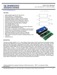
EDS-0090
OW-IO-DIO8
1-Wire Interface for 8 Discrete I/O
http://www.EmbeddedDataSystems.com
FEATURES
•
•
•
•
•
•
•
•
•
•
•
•
•
Has 8 connections; each may be an input and/or output.
Inputs accept up to 27 volts DC*.
Outputs are open drain and can sink up to 1 amp.
Connections have independently controlled pull-down resistors.
®
Compatible with all EDS and Maxim 1-Wire bus masters.
Uses 1-Wire communication protocol.
Input channels 1 and 2 report; pulse counts, activity latch & input states.
Input channels 3 to 8 report; activity latch and input states.
Optional Relay may be controlled independently or by alarm status.
LED may be controlled independently or by alarm status.
Support Conditional Search with user-selectable conditions.
Automatic unique 64-Bit device addressing.
Applications include thermostatic controls, industrial systems, flow meters, consumer products, or any system
in which discrete control or monitoring is necessary.
DESCRIPTION
The Octal Discrete I/O device offers an innovative way to monitor and control up to 8 digital channels. Each of
the 8 points may be an input or an output under program control. Additionally, each channel has an activity
latch, a programmable pulled-own resistor and programmable high / low alarms. Input channels 1 & 2 also
include 32 bit pulse counters.
The Octal Discrete I/O also includes an LED, conditional search support and an optional latching relay. These
features combine to offer a flexible system for monitoring and controlling numerous data points throughout a 1Wire network in an efficient manner. The conditional search support allows a host adapter to quickly identify
whether any alarm parameters have been met; and the LED and optional latching relay can be configured to
behave in a variety of ways:
•
•
•
Activate when an alarm becomes active and automatically deactivate when the alarm is cleared
Activate when within alarm parameters and deactivate when within normal range
Independently controlled
The nearly instant automated responses made by the LED and optional relay allows appropriate reactions
(activate fan/alarm siren/etc.) to occur before the monitoring application is even aware of an alarm. The Octal
Discrete I/O has been designed with the intention of simplifying the reading and control process; therefore any
general-purpose 1-Wire host adapters is capable of reading the discrete points.
* The maximum input voltage may be extended to 48 Volts by disabling the pull-down resistor.
Embedded Data Systems, LLC.; 2019 Fortune Drive; Lawrenceburg, KY 40342; Phone/Fax 502-859-5490
EN-USERMAN OW-IO-DIO8 V1.0 02.20.13
1-9
MEMORY MAP
The memory consists of three 32 byte pages. Page 0 is the tag, page 1 and 2 contain operational data. Pages 0, 1
and the first half of page 2 are read only, while the second half of page 2 can be written.
Page 0
Addr
0 - 27
28
29
30
31
Page 1
Addr
32
33
34
35
36
37
38
39
40
41
42
43
44
45
46
47
48
49
50
51
52
53
54
55
56
57
58
59
60
61
62
63
Page 2
Addr
64
65
66
67
68
69
b7
3
2
3
2
7
2
15
2
b6
2
2
2
2
6
2
14
2
b7
b5
1
2
1
2
5
2
13
2
b0
0
2
0
2
0
2
8
2
b2
2
12
2
5
5
5
5
2
11
2
4
4
4
4
2
10
2
3
3
3
3
b1
1
2
9
2
2
2
2
2
LED
b0
0
2
8
2
1
1
1
1
Rly
low 4
low 8
7
2
15
2
23
2
31
2
7
2
15
2
23
2
31
2
7
2
15
2
23
2
31
2
high 4
high 8
6
2
14
2
22
2
30
2
6
2
14
2
22
2
30
2
6
2
14
2
22
2
30
2
low 3
low 7
5
2
13
2
21
2
29
2
5
2
13
2
21
2
29
2
5
2
13
2
21
2
29
2
high 3
high 7
4
2
12
2
20
2
28
2
4
2
12
2
20
2
28
2
4
2
12
2
20
2
28
2
low 2
low 6
3
2
11
2
19
2
27
2
3
2
11
2
19
2
27
2
3
2
11
2
19
2
27
2
high 2
high 6
2
2
10
2
18
2
26
2
2
2
10
2
18
2
26
2
2
2
10
2
18
2
26
2
low 1
low 5
1
2
9
2
17
2
25
2
1
2
9
2
17
2
25
2
1
2
9
2
17
2
25
2
high 1
high 5
0
2
8
2
16
2
24
2
0
2
8
2
16
2
24
2
0
2
8
2
16
2
24
2
b7
b6
b5
4
b4
b3
b1
1
2
1
2
1
2
9
2
2
13
2
6
6
6
6
5
b4
b2
2
2
2
2
2
2
10
2
2
14
2
7
7
7
7
6
b5
b3
3
2
3
2
3
2
11
2
2
15
2
8
8
8
8
7
b6
b4
0
2
0
2
4
2
12
2
3
b3
2
b2
b1
Tag
Version, low
Version, high
ID, low
ID, high
R
R
R
R
R
ID, low
ID, high
Input states
Activity latch states
Output states
Pull-down states
Relay / LED State
Reserved
Reserved
Reserved
Alarm states
Reserved
Reserved
Reserved
Reserved
Reserved
Reserved
Reserved
Reserved
R
R
R
R
R
R
R
R
R
R
R
R
R
R
R
R
R
R
R
R
R
R
R
R
R
R
R
R
R
R
R
R
Reserved
Reserved
Reserved
Reserved
Reserved
Reserved
R
R
R
R
R
R
Seconds counter
Seconds counter
Seconds counter
Seconds counter
Pulse counter 1
Pulse counter 2
b0
Embedded Data Systems, LLC.; 2019 Fortune Drive; Lawrenceburg, KY 40342; Phone/Fax 502-859-5490
EN-USERMAN OW-IO-DIO8 V1.0 02.20.13
2-9
70
71
72
73
74
75
76
77
78
79
80
81
82
83
84
85
86
87
88
89
90
91
92
93
94
95
low 4
low 8
high 4
high 8
low 3
low 7
high 3
high 7
low 2
low 6
high 2
high 6
low 1
low 5
high 1
high 5
8
7
6
5
4
3
2
2
1
1
low 4
low 8
high 4
high 8
low 3
low 7
high 3
high 7
low 2
low 6
high 2
high 6
low 1
low 5
high 1
high 5
8
8
7
7
6
6
5
5
4
4
3
3
2
2
1
1
L1
L0
R1
LED
R0
Rly
Reserved
Reserved
Reserved
Reserved
Reserved
Reserved
Reserved
Reserved
Reserved
Reserved
Conditional search
Reserved
Reserved
Pulse counter reset
Activity latch reset
Reserved
Reserved
Alarm values
Reserved
Pull-down values (30)
Output values
Reserved
Relay / LED Function
Relay / LED value
R
R
R
R
R
R
R
R
R
R
RW
RW
RW
RW
RW
RW
RW
RW
RW
RW
RW
RW
RW
RW
RW
RW
* If the relay is not populated the bits pertaining to the Relay Function may be ignored.
INPUTS
The current input states are read using the Input states byte, location 34. The input state is de-bounced at 10ms,
making it useful to read contact closures. An activity latch (location 35) is maintained for each input. Any change in
state (high-to-low or low-to-high) causes the activity latch to be set. The activity latch states are detected by both
the input state logic (de-bounced at 10ms) and the pulse counter logic (channels 1 & 2 only). Since the pulse
counter logic is falling edge triggered only, a state change that is faster than what can be detected by the input
state logic will only trigger the activity latch if it contains a falling edge. Any or all of the bits in the activity latch can
be cleared, by writing to the Activity Latch Reset byte (location 85) with the desired bit or bits set; multiple bits can
be cleared at the same time. The activity latch reset byte always reads zero.
Input channels 1 & 2 include 32 bit pulse counters. The pulse is counted on the falling edge. Any counter can be
reset, by writing to the appropriate bit stored at pulse counter reset location (location 84). Each counter can handle
up to 40K per second. Contact the factory for applications that require faster pulse counting.
OUTPUTS
The outputs are open collector MOSFET transistors with unidirectional overvoltage TVS diodes (48 volt). When the
output state is high, the transistor is off. If there is pull-up current (such as a pull-up resistor), a voltmeter will read
high. When the output state is low, the transistor is on and the output will read low. Note that if there is no pull-up
current, the output may be off, but a voltmeter will not read high.
Output State byte, location 36, reflects the current output states, and is read only. Outputs are set, by writing to the
Output Value byte, location 92.
The Input State, Activity Latch and Pulse Counter values will continue to update if a point is used as an output, so
long as the voltage at the pin rises above the one threshold when the output transistor is turned off (i.e. there is a
pull-up resistor).
Embedded Data Systems, LLC.; 2019 Fortune Drive; Lawrenceburg, KY 40342; Phone/Fax 502-859-5490
EN-USERMAN OW-IO-DIO8 V1.0 02.20.13
3-9
PULL-DOWNS
Each pin has a 1.5k Ohm, 0.5 Watt pull-down resistor which may be turned on using the Pull-down value byte
(location 91). Setting a bit high turns off the pull-down, low turns it on. This resistor may be used to read contact
closures, simply connect one end of the contact to a voltage (i.e. 5, 12 or 25 volts) and the other end to the input
pin. When the contact is closed, the input will read a 1, when it is open the pull-down resistor will cause it to read 0.
The pull-down resistor should be turned off when a channel is being used as an output.
ALARMS
Alarms are based on the Input State; they are calculated every time a reading is made from the inputs. If the
reading is above the high alarm value, the corresponding high alarm bit is set, and if the reading is below the low
alarm value, the low alarm bit is set. Alarm bits can only be cleared by sending the clear alarms command (0x33),
which clears all alarm bits. No provision is made to clear individually selected alarm bits.
CONDITIONAL SEARCH
The device will respond to the conditional search command from a master if any or all of the conditional search bits
are set. The conditional search bits are set when an alarm becomes active and are cleared only under program
control, by writing to the appropriate bit(s) at location 80 and 81.
SECONDS COUNTER
The 32 bit counter (bytes 44 to 47) is set to zero at power up and increments approximately once per second.
RELAY AND LED
The relay and LED may operate in any of the following modes:
Bit L1 (LED)
or R1 (Relay)
0
0
1
1
Mode
(0) On with any alarm, off if no alarms active
(1) On with any alarm, off when clear alarms command received
(2) On and Off under command using State bit (address 95)
(3) Always off
Bit L0 (LED)
or R0 (Relay)
0
1
0
1
The relay is a latching relay; it retains its state when power is lost. The states of the relay and LED are stored in
non-volatile memory and are restored at power-up. Since the relay is latching, its state remains the same, even
when power is removed.
PROGRAMMABLE VALUES
Programmable values are stored in non-volatile memory.
Alarm High
Alarm Low
Pulse Counter Reset*
Activity Latch Reset*
Pull-down Value
Output Value
Factory Default
1
0
0
0
1
1
Minimum Value
0
0
0
0
0
0
Maximum Value
1
1
1
1
1
1
*These values always read zero. Writing a 1 to the appropriate bit causes the reset to occur, writing a 0 has no
effect.
1-WIRE COMMUNICATIONS
The device communicates via 1-wire at standard speed only; overdrive is not supported. All memory pages are 32
bytes, CRC16 and a 32 byte scratchpad is used to write data to the device.
ROM Commands
After the bus master has detected a presence pulse, it can issue a ROM command. These commands operate on
the unique 64-bit ROM codes of each slave device and allow the master to single out a specific device if many are
present on the 1-Wire bus. These commands also allow the master to determine how many and what types of
devices are present on the bus or if any device has experienced an alarm condition. There are five ROM
Embedded Data Systems, LLC.; 2019 Fortune Drive; Lawrenceburg, KY 40342; Phone/Fax 502-859-5490
EN-USERMAN OW-IO-DIO8 V1.0 02.20.13
4-9
commands, and each command is 8 bits long. The ROM commands function the same as on other 1-wire devices.
The master device must issue an appropriate ROM command before issuing a function command.
Alarm Search ROM – 0xEC
The operation of this command is identical to the operation of the Search ROM command except that only slaves
with a set alarm flag (bytes 80 and 81) will respond. This command allows the master device to determine if any
EDS Discrete I/O device is in an alarm. After every Alarm Search cycle (i.e., Alarm Search command followed by
data exchange), the bus master must return to Step 1 (Initialization) in the transaction sequence. See the
Operation—Alarm Signaling section for an explanation of alarm flag operation.
Search ROM – 0xF0
When a system is initially powered up, the master must identify the ROM codes of all slave devices on the bus,
which allows the master to determine the number of slaves and their device types. The master learns the ROM
codes through a process of elimination that requires the master to perform a Search ROM cycle (i.e., Search ROM
command followed by data exchange) as many times as necessary to identify all of the slave devices. If there is
only one slave on the bus, the simpler Read ROM command (see below) can be used in place of the Search ROM
process. For a detailed explanation of the Search ROM procedure, refer to the iButton® Book of Standards at
www.maxim-ic.com/ibuttonbook. After every Search ROM cycle, the bus master must return to Step 1 (Initialization)
in the transaction sequence.
Match ROM – 0x55
The match ROM command followed by a 64-bit ROM code sequence allows the bus master to address a specific
slave device on a multi-drop or single-drop bus. Only the slave that exactly matches the 64-bit ROM code
sequence will respond to the function command issued by the master; all other slaves on the bus will wait for a
reset pulse.
Skip ROM – 0xCC
The master can use this command to address all devices on the bus simultaneously without sending out any ROM
code information. For example, the master can clear all alarming EDS Environmental sensors on the bus or
perform simultaneous temperature conversions by issuing a Skip ROM command followed by a Clear alarms [0x33]
command.
Note that the Read Scratchpad [0xAA] command can follow the Skip ROM command only if there is a single slave
device on the bus. In this case, time is saved, by allowing the master to read from the slave without sending the
device’s 64-bit ROM code. A Skip ROM command followed by a Read Scratchpad command will cause a data
collision on the bus if there is more than one slave since multiple devices will attempt to transmit data
simultaneously.
Read ROM – 0x33
This command can only be used when there is one slave on the bus. It allows the bus master to read the slave’s
64-bit ROM code without using the Search ROM procedure. If this command is used when there is more than one
slave present on the bus, a data collision will occur when all the slaves attempt to respond at the same time.
Memory / Control Commands
Write scratchpad – 0x0F
Read scratchpad – 0xAA
Copy scratchpad – 0x55
Read memory no CRC – 0xF0
Read memory with CRC – 0xA5
Clear alarms – 0x33
Write Scratchpad – 0x0F
After issuing the Write Scratchpad command, the master must first provide the 2-byte target address, followed by
the data to be written to the scratchpad. The data will be written to the scratchpad starting at the byte offset (T4:T0).
The ending offset (E4:E0) will be the byte offset at which the master stops writing data. Only full data bytes are
accepted. If the last data byte is incomplete, its content will be ignored.
When executing the Write Scratchpad command, the CRC generator inside the device calculates a CRC of the
entire data stream, starting at the command code and ending at the last data byte sent by the master. This CRC is
generated using the CRC16 polynomial by first clearing the CRC generator and then shifting in the command code
Embedded Data Systems, LLC.; 2019 Fortune Drive; Lawrenceburg, KY 40342; Phone/Fax 502-859-5490
EN-USERMAN OW-IO-DIO8 V1.0 02.20.13
5-9
(0Fh) of the Write Scratchpad command, the Target Addresses TA1 and TA2 as supplied by the master and all the
data bytes. The master may end the Write Scratchpad command at any time. However, if the ending offset is
11111b, the master may send 16 read time slots and will receive an inverted CRC16 generated by the device.
Read Scratchpad – 0xAA
This command is used to verify scratchpad data and target address. After issuing the Read Scratchpad command,
the master begins reading. The first 2 bytes will be the target address. The next byte will be the ending offset/data
status byte (E/S) followed by the scratchpad data beginning at the byte offset (T4:T0). Regardless of the actual
ending offset, the master may read data until the end of the scratchpad after which it will receive an inverted
CRC16 of the command code, Target Addresses TA1 and TA2, the E/S byte, and the scratchpad data starting at
the target address. After the CRC is read, the bus master will read logical 1s from the device until a reset pulse is
issued.
Copy Scratchpad – 0x55
This command is used to copy data from the scratchpad to the writable memory sections. Applying Copy
Scratchpad to the Relay/LED State Byte can control the relay and/or LED provided that functionality has been
enabled (see Relay and LED section for details). After issuing the Copy Scratchpad command, the master must
provide a 3-byte authorization pattern, which can be obtained by reading the scratchpad for verification. This
pattern must exactly match the data contained in the three address registers (TA1, TA2, E/S, in that order). A
pattern of alternating 1s and 0s will be transmitted after the data has been copied until the master issues a reset
pulse.
The data to be copied is determined by the three address registers. The scratchpad data from the beginning offset
through the ending offset will be copied, starting at the target address. Anywhere from 1 to 32 bytes may be copied
to memory with this command.
Read Memory no CRC – 0xF0
The Read Memory command may be used to read the entire memory. After issuing the command, the master must
provide the 2-byte target address. After the 2 bytes, the master reads data beginning from the target address and
may continue until the end of memory, at which point logic 0s will be read. It is important to realize that the target
address registers will contain the address provided. The ending offset/data status byte is unaffected.
To safeguard data in the 1-Wire environment when reading and to simultaneously speed up data transfers, it is
recommended to make use of the Read Memory with CRC (0xA5) whenever possible. The 16-bit CRC ensures
rapid, error-free data transfers that eliminate having to read a page multiple times to verify whether if the received
data is correct.
Read Memory with CRC – 0xA5
The Read Memory with CRC command works essentially the same way as the simple Read Memory, except for the
16-bit CRC that the device generates and transmits following the last data byte of a memory page.
After having sent the command code of the Read Memory with CRC command, the bus master sends a 2-byte
address (TA1 = T7:T0, TA2 = T15:T8) that indicates a starting byte location. With the subsequent read data time
slots the master receives data from the device starting at the initial address and continuing until the end of a 32byte page is reached. At that point the bus master will send 16 additional read data time slots and receive an
inverted 16-bit CRC. With subsequent read data time slots the master will receive data starting at the beginning of
the next page followed again by the inverted CRC for that page. This sequence will continue until the bus master
resets the device.
With the initial pass through the Read Memory with CRC flow, the 16-bit CRC value is the result of shifting the
command byte into the cleared CRC generator followed by the 2 address bytes and the contents of the data
memory. Subsequent passes through the Read Memory with CRC flow will generate a 16-bit CRC that is the result
of clearing the CRC generator and then shifting in the contents of the data memory page. After the 16-bit CRC of
the last page is read, the bus master will receive logical 0s from the device until a reset pulse is issued.
Clear Alarms – 0x33
Embedded Data Systems, LLC.; 2019 Fortune Drive; Lawrenceburg, KY 40342; Phone/Fax 502-859-5490
EN-USERMAN OW-IO-DIO8 V1.0 02.20.13
6-9
The Clear Alarms command is used to set all bits at byte 54 to 0. The clearing the alarms has the ability to effect
relay state, and LED state depending on the configuration. Additional information on the possible effects is
available in Relay and LED and/or Conditional Search sections of the manual.
Family Code
The family code is 0x7E.
Tag
The tag provides identification for each EDS device type. It consists of three parts: the description, followed by the
firmware version number and then the device ID number. The description is the product name as an ASCII text
string; i.e. EDS0090 Octal Discrete IO. The firmware version is a 2 byte number provided in BCD format, LSB first.
For example: 0x36,0x01 represents the firmware version 1.36. The 2 byte device ID uniquely identifies this device
from others with the same family code. This is also presented in BCD format, LSB first. Therefore 0x90,0x00
represents Device ID 0090. The device ID portion of the tag is duplicated at the beginning of the next page so that
the user can read one page and retrieve all necessary information to work with the device.
3
2
3
2
7
2
15
2
2
2
2
2
6
2
14
2
1
2
1
2
5
2
13
2
0
2
0
2
4
2
12
2
3
2
3
2
3
2
11
2
2
2
2
2
2
2
10
2
1
2
1
2
1
2
9
2
0
2
0
2
0
2
8
2
Version, low
Version, high
ID, low
ID, high
CURRENT EDS DEVICE IDS
TAG ID
EDS0064
EDS0065
EDS0066
EDS0067
EDS0068
Tag Hex
Tag Bin (LSB first)
Features
0064
0065
0066
0067
0068
0110 0100 0000 0000
0110 0101 0000 0000
0110 0110 0000 0000
0110 0111 0000 0000
0110 1000 0000 0000
EDS0070
EDS0071
EDS0080
EDS0082
EDS0083
EDS0085
EDS0090
EDS0091
EDS0092
0070
0071
0080
0082
0083
0085
0090
0091
0092
0111 0000 0000 0000
0111 0001 0000 0000
1000 0000 0000 0000
1000 0010 0000 0000
1000 0011 0000 0000
1000 0101 0000 0000
1001 0000 0000 0000
1001 0001 0000 0000
1001 0010 0000 0000
Temp
Temp, humidity
Temp, barometric pressure
Temp, light
Temp, humidity, barometric
pressure and light
Vibration Sensor
RTD transmitter 4-Wire
Octal 4-20mA Input
Octal 0-10V Input
Quad 4-20mA Input
Quad 0-10V Input
Octal Discrete I/O
Quad Opto-isolator Input
Quad Relay Output
Embedded Data Systems, LLC.; 2019 Fortune Drive; Lawrenceburg, KY 40342; Phone/Fax 502-859-5490
EN-USERMAN OW-IO-DIO8 V1.0 02.20.13
7-9
SPECIFICATIONS
PARAMETER
MIN
TYP
MAX
UNITS
Operating Temperature Range
-40
-
85
°C
Input voltage
-3
-
27*
Volts
Input positive threshold
-
1.76
-
Volts
Input negative threshold
-
1.04
-
Volts
Input hysteresis
0.4
0.73
1.2
Volts
Pulse Counter Frequency
-
-
40K
Hertz
Output current sink
-
-
1
Amp
Relay Contacts Voltage Rating (DC)
-
-
220
Volts
Relay Contacts Switching Current Rating (DC)
Relay Contacts Carrying Current Rating (DC)
-
-
2
4
Amps
Amps
Relay Contacts Switching Power Rating (DC,
resistive load)
Relay Contacts Voltage Rating (AC)
-
-
30
Watts
-
-
250
Volts
Relay Contacts Switching Current Rating (AC)
-
-
2
Amps
Relay Contacts Carrying Current Rating(AC)
-
-
4
Amps
Relay Switching Power Rating (AC, resistive load)
-
-
62.5
VA
Supply Voltage
4
-
18
Volts DC
Active Current (5 volt supply, LED On)
-
18.2
-
mA
Standby Current (5 volt supply)
-
10.5
-
mA
Enclosure Dimensions (L x W x H)
4.109
2.233
1.594
Inches
INPUT CIRCUIT SCHEMATIC
* The maximum input voltage may be extended to 48 Volts by disabling the pull-down resistor.
Embedded Data Systems, LLC.; 2019 Fortune Drive; Lawrenceburg, KY 40342; Phone/Fax 502-859-5490
EN-USERMAN OW-IO-DIO8 V1.0 02.20.13
8-9
REGULATORY COMPLIANCE
FEDERAL COMMUNICATIONS COMMISSION (FCC) COMPLIANCE STATEMENT
This device complies with part 15 of the FCC Rules. Operation is subject to the following two
conditions: (1) This device may not cause harmful interference, and (2) this device must accept
any interference received, including interference that may cause undesired operation.
INDUSTRY CANADA (IC) COMPLIANCE STATEMENT
This Class B digital apparatus complies with Canadian ICES-003-2012.
Cet appareil numérique de la classe B est conforme à la norme NMB-003 du Canada.
EUROPEAN COMMUNITY (EC) DIRECTIVES CONFORMITY
APPLICATION OF COUNCIL DIRECTIVE 2004/108/EC Standard to which Conformity is
Declared:
EN 61326-1:2006
EN 61326-2-3:2006
EN 61000-3-2:2006+A1:2009+A2:2009
EN 61000-3-3:2008
(Emmissions)
(Immunity)
(Harmonics)
(Flicker)
Caution: The manufacturer is not responsible for any radio or television interference caused by using other than
recommended cables or by unauthorized changes or modifications to this equipment. Unauthorized changes or
modifications could void the user’s authority to operate this equipment.
ACKNOWLEDGEMENTS
®
1-Wire is a registered trademark of Maxim Integrated Products, Inc.
®
iButton is a registered trademark of Maxim Integrated Products, Inc.
Embedded Data Systems, LLC.; 2019 Fortune Drive; Lawrenceburg, KY 40342; Phone/Fax 502-859-5490
EN-USERMAN OW-IO-DIO8 V1.0 02.20.13
9-9