1
FUJITSU MICROELECTRONICS
CONTROLLER MANUAL
CM71-10146-1E
FR80
32-BIT MICROCONTROLLER
MB91660 Series
HARDWARE MANUAL
FR80
32-BIT MICROCONTROLLER
MB91660 Series
HARDWARE MANUAL
The information for microcontroller supports is shown in the following homepage.
Be sure to refer to the "Check Sheet" for the latest cautions on development.
"Check Sheet" is seen at the following support page
"Check Sheet" lists the minimal requirement items to be checked to prevent problems beforehand in system development.
http://edevice.fujitsu.com/micom/en-support/
FUJITSU MICROELECTRONICS LIMITED
MB91660 Series
Preface
Thank you for your continued use of Fujitsu microelectronics semiconductor products.
Read this manual and "Data Sheet" thoroughly before using products in the MB91660 series.
■ Purpose of this manual and intended readers
This manual explains the functions and operations of the MB91660 series and describes how it is used.
The manual is intended for engineers engaged in the actual development of products using the MB91660
series.
Note: FR is an abbreviation for the FUJITSU RISC controller, which is a product of Fujitsu
Microelectronics Limited.
■ Trademark
The company names and brand names herein are the trademarks or registered trademarks of their
respective owners.
■ License
Purchase of Fujitsu I2C components conveys a license under the Philips I2C Patent Rights to use, these
components in an I2C system provided that the system conforms to the I2C Standard Specification as
defined by Philips.
■ Sample programs and development environment
Fujitsu Microelectronics offers sample programs free of charge for using the peripheral functions of the
FR80 family. Fujitsu Microelectronics also makes available descriptions of the development environment
required for the MB91660 series. Feel free to use them to verify the operational specifications and usage
of this Fujitsu microelectronics microcontroller.
• Microcontroller support information:
http://edevice.fujitsu.com/micom/en-support/
* Note that the sample programs are subject to change without notice. Since they are offered as a way to
demonstrate standard operations and usage, evaluate them sufficiently before running them on your
system.
Fujitsu microelectronics assumes no responsibility for any damage that may occur as a result of using a
sample program.
CM71-10146-1E
FUJITSU MICROELECTRONICS LIMITED
i
MB91660 Series
•
•
•
•
•
•
•
The contents of this document are subject to change without notice.
Customers are advised to consult with sales representatives before ordering.
The information, such as descriptions of function and application circuit examples, in this document are presented
solely for the purpose of reference to show examples of operations and uses of FUJITSU MICROELECTRONICS
device; FUJITSU MICROELECTRONICS does not warrant proper operation of the device with respect to use
based on such information. When you develop equipment incorporating the device based on such information, you
must assume any responsibility arising out of such use of the information. FUJITSU MICROELECTRONICS
assumes no liability for any damages whatsoever arising out of the use of the information.
Any information in this document, including descriptions of function and schematic diagrams, shall not be
construed as license of the use or exercise of any intellectual property right, such as patent right or copyright, or
any other right of FUJITSU MICROELECTRONICS or any third party or does FUJITSU MICROELECTRONICS
warrant non-infringement of any third-party's intellectual property right or other right by using such information.
FUJITSU MICROELECTRONICS assumes no liability for any infringement of the intellectual property rights or
other rights of third parties which would result from the use of information contained herein.
The products described in this document are designed, developed and manufactured as contemplated for general
use, including without limitation, ordinary industrial use, general office use, personal use, and household use, but
are not designed, developed and manufactured as contemplated (1) for use accompanying fatal risks or dangers
that, unless extremely high safety is secured, could have a serious effect to the public, and could lead directly to
death, personal injury, severe physical damage or other loss (i.e., nuclear reaction control in nuclear facility,
aircraft flight control, air traffic control, mass transport control, medical life support system, missile launch control
in weapon system), or (2) for use requiring extremely high reliability (i.e., submersible repeater and artificial
satellite).
Please note that FUJITSU MICROELECTRONICS will not be liable against you and/or any third party for any
claims or damages arising in connection with above-mentioned uses of the products.
Any semiconductor devices have an inherent chance of failure. You must protect against injury, damage or loss
from such failures by incorporating safety design measures into your facility and equipment such as redundancy,
fire protection, and prevention of over-current levels and other abnormal operating conditions.
Exportation/release of any products described in this document may require necessary procedures in accordance
with the regulations of the Foreign Exchange and Foreign Trade Control Law of Japan and/or US export control
laws.
The company names and brand names herein are the trademarks or registered trademarks of their respective
owners.
Copyright ©2008 FUJITSU MICROELECTRONICS LIMITED All rights reserved.
ii
FUJITSU MICROELECTRONICS LIMITED
CM71-10146-1E
MB91660 Series
Manuals That Make Up the Manuals for This Series
The manuals used for this series are listed below. See the manual appropriate to the applicable
conditions.
The contents of these manuals are subject to change without notice. Contact us to check the latest
versions available.
■ Hardware manual
• FR80 FAMILY MB91660 SERIES HARDWARE MANUAL (CM71-10146-1E) (this manual)
■ Data sheet
• MICROCONTROLLER 32-bit ORIGINAL FR80 FAMILY MB91660 SERIES DATA SHEET
(DS07-16905-1E)
■ Programming manual
• FR80 FAMILY PROGRAMMING MANUAL (CM71-00102-1E)
This manual explains a programming model and instructions for the FR80 family CPUs.
■ Hardware tool-related manual
• DSU-FR EMULATOR MB2198-01 HARDWARE MANUAL (CM71-00413-2E)
This manual explains emulator handling and specifications, and it explains how to connect and operate
the emulator.
■ Software tool-related manuals
• SOFTUNETM WORKBENCH OPERATION MANUAL for V6 (CM71-00328-3E)
This manual explains how to operate the integrated development environment called SOFTUNE and
the development procedures.
• SOFTUNETM WORKBENCH USER'S MANUAL for V6 (CM71-00329-3E)
This manual explains the basic functions and dependent functions of SOFTUNE Workbench.
• SOFTUNETM WORKBENCH COMMAND REFERENCE MANUAL for V6 (CM71-00330-3E)
This manual explains the commands and built-in variables/functions of SOFTUNE Workbench.
• FR FAMILY 32-BIT MICROCONTROLLER EMBEDDED C PROGRAMMING MANUAL FOR
APPLICATION (CM71-00324-1E)
This manual describes the know-how for creating built-in systems using the C compiler fcc911 for the
FR family. The manual explains how to create efficient C programs using the architecture of the FR
family and provides the notes.
• FR FAMILY SOFTUNE C/C++ COMPILER MANUAL for V6 (CM81-00206-3E)
Refer to this manual when using SOFTUNE C/C++ compiler to create/develop application programs in
C and C++.
• FR FAMILY SOFTUNETM ASSEMBLER MANUAL for V6 (CM71-00203-3E)
This manual explains the functions of Fujitsu SOFTUNETM Assembler operating in Windows 98,
Windows Me, Windows 2000, or Windows XP and how to use it.
CM71-10146-1E
FUJITSU MICROELECTRONICS LIMITED
iii
MB91660 Series
• SOFTUNETM LINKAGE KIT MANUAL for V6 (CM71-00327-3E)
This manual explains the functions of Fujitsu SOFTUNETM Linkage Kit operating in Windows 98,
Windows Me, Windows 2000, or Windows XP and how to use it.
See the manual when developing an application program.
• FR Family ABSOLUTE ASSEMBLY LIST GENERATOR TOOL MANUAL (CM71-00305-2E)
This manual explains absolute assemble lists.
• FR-V/FR FAMILY SOFTUNE C/C++ ANALYZER MANUAL for V5 (CM81-00309-4E)
This manual explains the functions of C/C++ Analyzer and how to use it.
• FR-V/FR FAMILY SOFTUNE C/C++ CHECKER MANUAL for V5 (CM81-00310-4E)
This manual explains the functions of C/C++ Checker and how to use it.
■ REALOS-related manuals
● REALOS µITRON3.0-related manuals
• FR/F2MC FAMILY IN CONFORMANCE WITH µITRON SPECIFICATIONS SOFTUNETM
REALOSTM/FR/907/896 CONFIGURATOR MANUAL (CM71-00322-5E)
This manual explains the functions and operations of SOFTUNE REALOS Configurator.
• FR-V/FR/F2MC FAMILY IN CONFORMANCE WITH µITRON SPECIFICATIONS SOFTUNETM
REALOSTM/ANALYZER MANUAL (CM81-00315-3E)
This manual explains the functions provided by SOFTUNE REALOS Analyzer and how to utilize the
functions.
• FR FAMILY IN CONFORMANCE WITH µITRON 3.0 SPECIFICATIONS SOFTUNE REALOS/
FR USER'S GUIDE (CM71-00320-3E)
This manual explains the configuration/activation of REALOS/FR application systems.
See the manual when performing comprehensive work for an entire system.
• FR FAMILY IN CONFORMANCE WITH µITRON 3.0 SPECIFICATIONS SOFTUNE REALOS/
FR KERNEL MANUAL (CM71-00321-3E)
This manual explains the functions provided by SOFTUNE REALOS/FR and how to utilize the
functions.
See the manual when creating an application system or user program.
● REALOS µITRON4.0-related manuals
• FR FAMILY IN CONFORMANCE WITH µITRON 4.0 SPECIFICATIONS SOFTUNETM
REALOSTM/FR Spec.4 PROGRAMMING MANUAL (CM81-00316-1E)
This manual explains the functions provided by SOFTUNE REALOS/FR Spec.4 and how to utilize the
functions.
• FR-V/FR FAMILY IN CONFORMANCE WITH µITRON 4.0 SPECIFICATIONS SOFTUNETM
REALOSTM KERNEL MANUAL (CM81-00312-2E)
This manual explains the functions provided by SOFTUNE REALOS/FRV/FR Spec.4 and how to
utilize the functions.
• FR-V/FR FAMILY IN CONFORMANCE WITH µITRON 4.0 SPECIFICATIONS SOFTUNETM
REALOSTM CONFIGURATOR MANUAL (CM81-00311-3E)
This manual explains the functions provided by SOFTUNE REALOS Configurator (GUI) and how to
utilize the functions.
iv
FUJITSU MICROELECTRONICS LIMITED
CM71-10146-1E
MB91660 Series
• FR-V/FR /F2MC FAMILY IN CONFORMANCE WITH µITRON SPECIFICATIONS SOFTUNE
REALOSTM ANALYZER MANUAL (CM81-00315-3E)
This manual explains the functions provided by SOFTUNE REALOS Analyzer and how to utilize the
functions.
CM71-10146-1E
FUJITSU MICROELECTRONICS LIMITED
v
MB91660 Series
How to Use This Manual
■ Finding a function
The following methods can be used to search for the explanation of a desired function in this manual:
• Search from the table of the contents
The table of the contents lists the manual contents in the order of description.
• Search from the register list
The register list lists all the registers of this device. You can look up the name of a desired register on
the list to find the address of its location or the page that explains it.
The address where each register is located is not described in the text. To verify the address of a
register, see "APPENDIX A I/O Map", and "APPENDIX B List of Registers".
• Search from the index
You can look up the keyword such as the name of a peripheral function in the index to find the
explanation of the function.
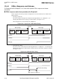
■ About the chapters
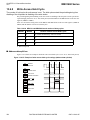
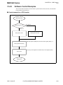
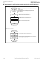
Basically, this manual explains 1 peripheral function per chapter.
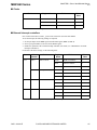
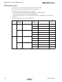
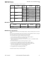
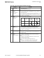
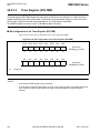
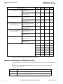
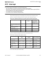
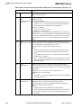
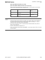
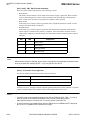
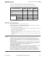
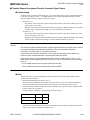
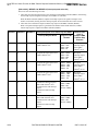
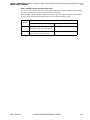
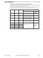
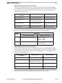
■ Terminology
This manual uses the following terminology.
Term
vi
Explanation
Word
Indicates access in units of 32 bits.
Half word
Indicates access in units of 16 bits.
Byte
Indicates access in units of 8 bits.
FUJITSU MICROELECTRONICS LIMITED
CM71-10146-1E
MB91660 Series
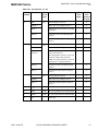
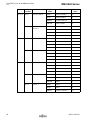
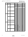
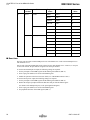
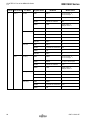
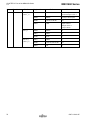
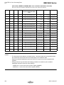
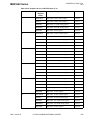
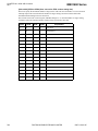
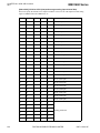
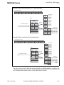
CONTENTS
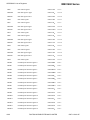
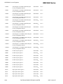
CHAPTER 1
1.1
1.2
1.3
1.4
CHAPTER 2
2.1
2.2
2.3
2.4
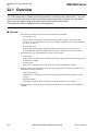
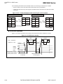
Overview ........................................................................................................1
MB91660 Series Overview .....................................................................................................................2
MB91660 Series Product Configuration .................................................................................................7
MB91660 Series Block Diagram .............................................................................................................9
Package Dimensions ............................................................................................................................10
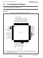
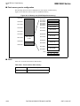
Pins of the MB91660 Series .......................................................................11
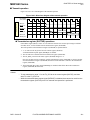
Pin Assignment Diagram ......................................................................................................................12
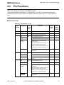
Pin Functions ........................................................................................................................................13
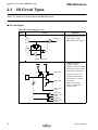
I/O Circuit Types ...................................................................................................................................38
Setting Method for Pins ........................................................................................................................44
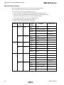
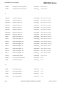
CHAPTER 3
CPU ..............................................................................................................91
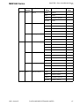
3.1 Memory Space ......................................................................................................................................92
3.2 Features of the Internal Architecture ....................................................................................................94
3.3 Operation Modes ..................................................................................................................................95
3.4 Pipeline .................................................................................................................................................96
3.5 Overview of Instructions .......................................................................................................................98
3.5.1 Arithmetic Operation ........................................................................................................................98
3.5.2 Load and Store ................................................................................................................................98
3.5.3 Branch .............................................................................................................................................99
3.5.4 Logical Operation and Bit Operation ...............................................................................................99
3.5.5 Direct Addressing ............................................................................................................................99
3.5.6 Bit Search ........................................................................................................................................99
3.5.7 Other ................................................................................................................................................99
3.6 Basic Programming Model ..................................................................................................................100
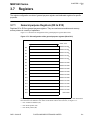
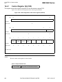
3.7 Registers .............................................................................................................................................101
3.7.1 General-purpose Registers (R0 to R15) ........................................................................................101
3.7.2 Program Status Register (PS) .......................................................................................................102
3.7.3 Program Counter (PC) ...................................................................................................................107
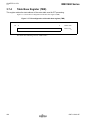
3.7.4 Table Base Register (TBR) ...........................................................................................................108
3.7.5 Return Pointer (RP) .......................................................................................................................109
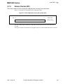
3.7.6 System Stack Pointer (SSP) ..........................................................................................................110
3.7.7 User Stack Pointer (USP) ..............................................................................................................111
3.7.8 Multiply & Divide Registers ............................................................................................................112
3.8 Data Configuration ..............................................................................................................................113
3.8.1 Bit Ordering ...................................................................................................................................113
3.8.2 Byte Ordering ................................................................................................................................114
3.8.3 Word Alignment .............................................................................................................................115
3.9 Addressing ..........................................................................................................................................116
3.9.1 Direct Addressing Areas ................................................................................................................116
3.9.2 20-bit Addressing Area ..................................................................................................................117
3.9.3 32-bit Addressing Area ..................................................................................................................117
3.9.4 Vector Table Initial Area ................................................................................................................117
CM71-10146-1E
FUJITSU MICROELECTRONICS LIMITED
vii
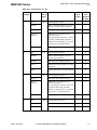
MB91660 Series
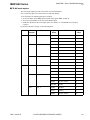
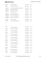
3.10 Branch Instructions ............................................................................................................................ 118
3.10.1 Operation with Delay Slots ........................................................................................................... 118
3.10.2 Operation without Delay Slots ...................................................................................................... 120
3.11 EIT (Exception, Interrupt, Trap) ......................................................................................................... 121
3.11.1 EIT Sources .................................................................................................................................. 121
3.11.2 Return from EIT ............................................................................................................................ 121
3.11.3 Interrupt Level ............................................................................................................................... 122
3.11.4 I Flag ............................................................................................................................................. 123
3.11.5 Interrupt Level Mask Register (ILM) ............................................................................................. 124
3.11.6 Level Mask for Interrupts .............................................................................................................. 124
3.11.7 Interrupt Control Register (ICR) .................................................................................................... 125
3.11.8 System Stack Pointer (SSP) ......................................................................................................... 125
3.11.9 Interrupt Stack .............................................................................................................................. 125
3.11.10 Table Base Register (TBR) ........................................................................................................... 126
3.11.11 EIT Vector Table ........................................................................................................................... 126
3.11.12 Multi-EIT Processing ..................................................................................................................... 127
3.11.13 Operation ...................................................................................................................................... 128
3.11.14 INT Instruction Operation .............................................................................................................. 129
3.11.15 INTE Instruction Operation ........................................................................................................... 130
3.11.16 Step Trace Trap Operation ........................................................................................................... 130
3.11.17 Undefined Instruction Exception Operation .................................................................................. 131
3.11.18 RETI Instruction Operation ........................................................................................................... 131
3.11.19 Delay Slots and EIT ...................................................................................................................... 131
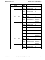
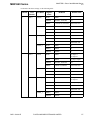
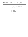
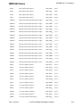
CHAPTER 4
Clock Generating Parts ............................................................................ 133
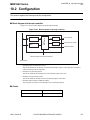
4.1 Overview ............................................................................................................................................ 134
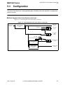
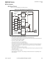
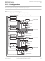
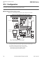
4.2 Configuration ..................................................................................................................................... 135
4.2.1 Clock Generating Parts ................................................................................................................. 135
4.2.2 Source Clock (SRCCLK) Selection Block ..................................................................................... 138
4.3 Pins .................................................................................................................................................... 139
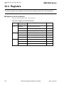
4.4 Registers ............................................................................................................................................ 140
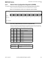
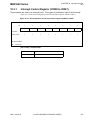
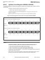
4.4.1 Clock Source Select Register (CSELR) ........................................................................................ 141
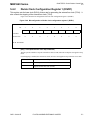
4.4.2 Clock Source Monitor Register (CMONR) .................................................................................... 145
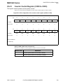
4.4.3 Clock Stabilization Time Select Register (CSTBR) ...................................................................... 148
4.4.4 PLL Configuration Register (PLLCR) ............................................................................................ 151
4.5 Explanation of Operations ................................................................................................................. 155
4.5.1 Explanation of Clock Source Operations ...................................................................................... 155
4.5.2 Switching the Source Clock (SRCCLK) ....................................................................................... 158
4.5.3 Multiple Rate for Generating the PLL Clock (PLLCLK) ................................................................. 161
CHAPTER 5
Clock Division Control Part ..................................................................... 163
5.1 Overview ............................................................................................................................................ 164
5.2 Internal Clocks ................................................................................................................................... 165
5.3 Configuration ..................................................................................................................................... 167
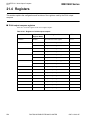
5.4 Registers ............................................................................................................................................ 168
5.4.1 Divide Clock Configuration Register 0 (DIVR0) ............................................................................ 169
5.4.2 Divide Clock Configuration Register 1 (DIVR1) ............................................................................ 171
5.4.3 Divide Clock Configuration Register 2 (DIVR2) ............................................................................ 173
5.5 Division Rate ...................................................................................................................................... 175
viii
FUJITSU MICROELECTRONICS LIMITED
CM71-10146-1E
MB91660 Series
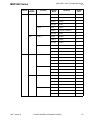
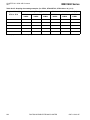
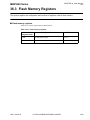
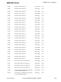
CHAPTER 6
Main Timer .................................................................................................177
6.1 Overview .............................................................................................................................................178
6.2 Configuration ......................................................................................................................................179
6.3 Registers .............................................................................................................................................180
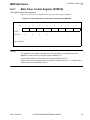
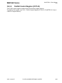
6.3.1 Main Timer Control Register (MTMCR) .........................................................................................181
6.4 Interrupts ............................................................................................................................................185
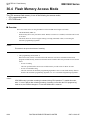
6.5 An Explanation of Operations and Setting Procedure Examples .......................................................186
6.5.1 Main Timer Operation ....................................................................................................................186
6.5.2 Transition to Stop Mode ................................................................................................................188
CHAPTER 7
Sub Timer ..................................................................................................189
7.1 Overview .............................................................................................................................................190
7.2 Configuration ......................................................................................................................................191
7.3 Registers .............................................................................................................................................192
7.3.1 Sub Timer Control Register (STMCR) ...........................................................................................193
7.4 Interrupts ............................................................................................................................................197
7.5 An Explanation of Operations and Setting Procedure Examples .......................................................198
7.5.1 Sub timer operation .......................................................................................................................198
7.5.2 Transition to Stop Mode, and Watch Mode ...................................................................................200
CHAPTER 8
Low-power Dissipation Mode ..................................................................201
8.1 Overview .............................................................................................................................................202
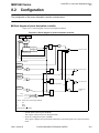
8.2 Configuration ......................................................................................................................................203
8.3 Registers .............................................................................................................................................205
8.3.1 Standby Mode Control Register (STBCR) .....................................................................................206
8.3.2 Sleep Rate Configuration Register (SLPRR) .................................................................................209
8.4 An Explanation of Operations and Setting Procedure Examples .......................................................211
8.4.1 Operation When Clock Control Is Set ............................................................................................212
8.4.2 Operation in Doze Mode ................................................................................................................214
8.4.3 Operation in Sleep Mode ...............................................................................................................215
8.4.4 Operation in Main Timer Mode ......................................................................................................218
8.4.5 Operation in Watch Mode ..............................................................................................................220
8.4.6 Operation in Stop Mode .................................................................................................................222
8.5 Notes on Use ......................................................................................................................................225
CHAPTER 9
Reset ..........................................................................................................227
9.1 Overview .............................................................................................................................................228
9.2 Configuration ......................................................................................................................................229
9.3 Pins .....................................................................................................................................................231
9.4 Registers .............................................................................................................................................232
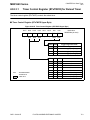
9.4.1 Reset Result Register (RSTRR) ....................................................................................................233
9.4.2 Reset Control Register (RSTCR) ..................................................................................................235
9.5 Explanation of Operations ..................................................................................................................237
9.5.1 Reset Types ..................................................................................................................................237
9.5.2 Reset Resource .............................................................................................................................238
9.5.3 Operation of Reset ........................................................................................................................239
9.6 Operating State and Transition ...........................................................................................................244
CM71-10146-1E
FUJITSU MICROELECTRONICS LIMITED
ix
MB91660 Series
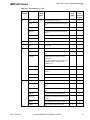
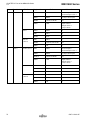
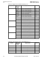
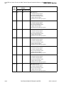
CHAPTER 10 Interrupt Controller .................................................................................. 249
10.1 Overview ............................................................................................................................................ 250
10.2 Configuration ..................................................................................................................................... 251
10.3 Registers ............................................................................................................................................ 252
10.3.1 Interrupt Control Register (ICR00 to ICR47) ................................................................................. 253
10.4 An Explanation of Operations and Setting Procedure Examples ....................................................... 255
10.4.1 Explanation of Operations of Interrupt Controller ......................................................................... 255
10.5 Notes on Use ..................................................................................................................................... 257
CHAPTER 11 Interrupt Request Batch-Read Function ................................................ 259
11.1 Overview ............................................................................................................................................ 260
11.2 Configuration ..................................................................................................................................... 261
11.3 Registers ............................................................................................................................................ 262
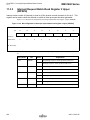
11.3.1 Interrupt Request Batch-Read Register 0 Upper (IRPR0H) ......................................................... 263
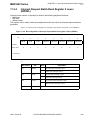
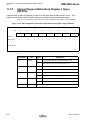
11.3.2 Interrupt Request Batch-Read Register 1 Upper/Lower (IRPR1H/ IRPR1L) ................................ 265
11.3.3 Interrupt Request Batch-Read Register 2 Upper (IRPR2H) ......................................................... 268
11.3.4 Interrupt Request Batch-Read Register 2 Lower (IRPR2L) .......................................................... 269
11.3.5 Interrupt Request Batch-Read Register 3 Upper (IRPR3H) ......................................................... 270
11.3.6 Interrupt Request Batch-Read Register 3 Lower (IRPR3L) .......................................................... 271
11.3.7 Interrupt Request Batch-Read Register 4 Upper (IRPR4H) ......................................................... 272
11.3.8 Interrupt Request Batch-Read Register 4 Lower (IRPR4L) .......................................................... 273
11.3.9 Interrupt Request Batch-Read Register 5 Upper (IRPR5H) ......................................................... 275
11.3.10 Interrupt Request Batch-Read Register 5 Lower (IRPR5L) .......................................................... 277
11.3.11 Interrupt Request Batch-Read Register 6 Upper (IRPR6H) ......................................................... 279
11.3.12 Interrupt Request Batch-Read Register 6 Lower (IRPR6L) .......................................................... 281
11.3.13 Interrupt Request Batch-Read Register 7 Upper (IRPR7H) ......................................................... 283
11.3.14 Interrupt Request Batch-Read Register 7 Lower (IRPR7L) .......................................................... 285
11.4 Notes on Use ..................................................................................................................................... 286
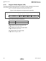
CHAPTER 12 Delay Interrupt .......................................................................................... 287
12.1 Overview ............................................................................................................................................ 288
12.2 Configuration ..................................................................................................................................... 289
12.3 Registers ............................................................................................................................................ 290
12.3.1 Delayed Interrupt Control Register (DICR) ................................................................................... 291
12.4 An Explanation of Operations and Setting Procedure Examples ....................................................... 292
12.4.1 Explanation of Delay Interrupt Operations .................................................................................... 292
12.5 Notes on Use ..................................................................................................................................... 293
CHAPTER 13 External Bus Interface ............................................................................. 295
13.1 Overview ............................................................................................................................................ 296
13.2 Configuration ..................................................................................................................................... 298
13.3 Pins .................................................................................................................................................... 300
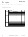
13.4 Registers ............................................................................................................................................ 302
13.4.1 Area Setting Registers (ASR0 to ASR3) ....................................................................................... 303
13.4.2 Area Configuration Registers (ACR0 to ACR3) ............................................................................ 306
13.4.3 Area Wait Registers (AWR0 to AWR3) ......................................................................................... 309
13.4.4 DMA Transfer Registers (DMAR0 to DMAR3) .............................................................................. 318
13.5 Protocols ............................................................................................................................................ 320
13.5.1 Address Data Split Bus Protocol ................................................................................................... 320
x
FUJITSU MICROELECTRONICS LIMITED
CM71-10146-1E
MB91660 Series
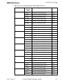
13.5.2 Address Data Multiplex Bus Protocol ............................................................................................326
13.6 Timing Settings ...................................................................................................................................332
13.6.1 Read Access Automatic Wait ........................................................................................................333
13.6.2 Write Access Automatic Wait ........................................................................................................336
13.6.3 Read Access Idle Cycle .................................................................................................................339
13.6.4 Write Recovery Cycle ....................................................................................................................342
13.6.5 Read Access Setup Cycle .............................................................................................................345
13.6.6 Read Access Hold Cycle ...............................................................................................................347
13.6.7 Write Access Setup Cycle .............................................................................................................350
13.6.8 Write Access Hold Cycle ...............................................................................................................352
13.6.9 Chip Select Delay Cycle ................................................................................................................354
13.6.10 Address Output Extension Cycle ...................................................................................................357
13.6.11 Address Strobe Output Extension Cycle .......................................................................................359
13.7 Access Cycle Extension Using the RDY Pin ......................................................................................362
13.8 Number of Access Cycles ...................................................................................................................365
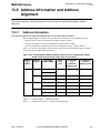
13.9 Address Information and Address Alignment .....................................................................................367
13.9.1 Address Information ......................................................................................................................367
13.9.2 Address Alignment ........................................................................................................................368
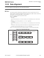
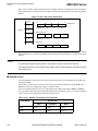
13.10 Data Alignment ...................................................................................................................................369
13.10.1 Big Endian .....................................................................................................................................371
13.10.2 Little Endian ...................................................................................................................................375
13.11 External Bus DMA Transfer ................................................................................................................379
13.11.1 Transfer Requests with the DREQ0 to DREQ3 Pins .....................................................................380
13.11.2 Transfer Request Acceptance with the DACK0 to DACK3 Pins ....................................................384
13.11.3 Transfer End Signal by the DEOP0 to DEOP3 Pins ......................................................................386
13.12 CS Area Setting Procedure ................................................................................................................387
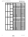
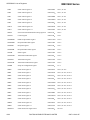
CHAPTER 14 Slave Interface ..........................................................................................393
14.1 Overview .............................................................................................................................................394
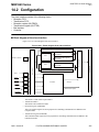
14.2 Configuration ......................................................................................................................................395
14.3 Pins .....................................................................................................................................................397
14.4 Registers .............................................................................................................................................399
14.4.1 Control Register (SLIFCR) ............................................................................................................400
14.4.2 Status Register (SLIFSR) ..............................................................................................................404
14.4.3 Reception FIFO Status Register (SLIFRXSR) ...............................................................................408
14.4.4 Transmission FIFO Status Register (SLIFTXSR) ..........................................................................410
14.4.5 Reception FIFO Data Register (SLIFRXDR) .................................................................................411
14.4.6 Transmission FIFO Data Register (SLIFTXDR) ............................................................................412
14.4.7 Reception Register (SLIFRXR) .....................................................................................................413
14.4.8 Transmission Register (SLIFTXR) .................................................................................................414
14.4.9 DMA Reception FIFO Register (SLIFDRXR) .................................................................................415
14.5 Interrupts ............................................................................................................................................416
14.6 Explanation of Operations and Setting Procedure Examples .............................................................418
14.6.1 Explanation of Operations of the Slave Interface ..........................................................................418
14.7 Notes on Use ......................................................................................................................................423
CHAPTER 15 I/O Ports .....................................................................................................425
15.1 Overview .............................................................................................................................................426
15.2 Configuration ......................................................................................................................................428
CM71-10146-1E
FUJITSU MICROELECTRONICS LIMITED
xi
MB91660 Series
15.3 Pins .................................................................................................................................................... 433
15.4 Registers ............................................................................................................................................ 434
15.4.1 Port Data Direction Registers (DDR0 to DDRK) ........................................................................... 436
15.4.2 Port Function Registers (PFR0 to PFRH) ..................................................................................... 439
15.4.3 Extended Port Function Registers (EPFR0 to EPFR35) .............................................................. 442
15.4.4 Port Data Registers (PDR0 to PDRK) .......................................................................................... 463
15.4.5 Pull-up Resistor Control Registers (PCR0 to PCRK) .................................................................... 465
15.4.6 A/D Channel Enable Register (ADCHE) ....................................................................................... 467
15.5 Notes on Use ..................................................................................................................................... 468
CHAPTER 16 External Interrupt Controllers ................................................................. 471
16.1 Overview ............................................................................................................................................ 472
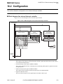
16.2 Configuration ..................................................................................................................................... 473
16.3 Pins .................................................................................................................................................... 475
16.4 Registers ............................................................................................................................................ 476
16.4.1 External Interrupt Request Level Registers (ELVR0 to ELVR3) ................................................... 477
16.4.2 External Interrupt Request Registers (EIRR0 to EIRR3) .............................................................. 480
16.4.3 Enable Interrupt Request Registers (ENIR0 to ENIR3) ................................................................ 482
16.5 Explanation of Operations and Setting Procedure Examples ............................................................ 484
16.5.1 Operations of the External Interrupt Controllers ........................................................................... 484
16.5.2 Return from Standby Mode ........................................................................................................... 487
16.5.3 Return from Sleep Mode ............................................................................................................... 489
CHAPTER 17 Watchdog Timer ....................................................................................... 491
17.1 Overview ............................................................................................................................................ 492
17.2 Configuration ..................................................................................................................................... 493
17.3 Registers ............................................................................................................................................ 495
17.3.1 Watchdog Timer Control Register 0 (WDTCR0) ........................................................................... 496
17.3.2 Watchdog Timer Clear Pattern Register 0 (WDTCPR0) ............................................................... 499
17.4 Explanation of Operations and Setting Procedure Examples ............................................................ 500
17.4.1 Operations of the Watchdog Timer ............................................................................................... 500
CHAPTER 18 Watch Counter .......................................................................................... 503
18.1 Overview ............................................................................................................................................ 504
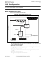
18.2 Configuration ..................................................................................................................................... 505
18.3 Registers ............................................................................................................................................ 507
18.3.1 Watch Counter Reload Register (WCRL) ..................................................................................... 508
18.3.2 Watch Counter Control Register (WCCR) .................................................................................... 509
18.3.3 Watch Counter Read Register (WCRD) ....................................................................................... 512
18.4 Interrupts ............................................................................................................................................ 513
18.5 Explanation of Operations and Setting Procedure Examples ............................................................ 514
18.5.1 Operations of the Watch Counter ................................................................................................. 514
18.6 Notes on Use ..................................................................................................................................... 516
CHAPTER 19 32-bit Free-Run Timer .............................................................................. 517
19.1
19.2
19.3
19.4
xii
Overview ............................................................................................................................................ 518
Configuration ..................................................................................................................................... 519
Pins .................................................................................................................................................... 523
Registers ............................................................................................................................................ 524
FUJITSU MICROELECTRONICS LIMITED
CM71-10146-1E
MB91660 Series
19.4.1 Free-Run Timer Select Register (FRTSEL) ...................................................................................525
19.4.2 Compare Clear Register (CPCLR0, CPCLR1) ..............................................................................526
19.4.3 Timer Data Register (TCDT0, TCDT1) ..........................................................................................527
19.4.4 Timer Status Control Register Upper/Lower (TCCSH0/TCCSL0, TCCSH1/TCCSL1) ..................528
19.5 Interrupts ............................................................................................................................................532
19.6 An Explanation of Operations and Setting Procedure Examples .......................................................533
19.6.1 Operation When an Internal Clock (Peripheral Clock) Is Selected ................................................534
19.6.2 Operation When an External Clock Is Selected ............................................................................535
CHAPTER 20 32-bit Input Capture ..................................................................................537
20.1 Overview .............................................................................................................................................538
20.2 Configuration ......................................................................................................................................539
20.3 Pins .....................................................................................................................................................541
20.4 Registers .............................................................................................................................................542
20.4.1 Input Capture Status Control Registers (ICS01 to ICS67) ............................................................543
20.4.2 Input Capture Data Register (IPCP0 to IPCP7) .............................................................................547
20.5 Interrupts ............................................................................................................................................548
20.6 An Explanation of Operations and Setting Procedure Examples .......................................................549
20.6.1 Explanation of 32-bit Input Capture Operation ..............................................................................549
CHAPTER 21 32-bit Output Compare .............................................................................553
21.1 Overview .............................................................................................................................................554
21.2 Configuration ......................................................................................................................................555
21.3 Pins .....................................................................................................................................................557
21.4 Registers .............................................................................................................................................558
21.4.1 Output Compare Register (OCCP0 to OCCP7) ............................................................................559
21.4.2 Compare Control Register Upper (OCSH1, OCSH3, OCSH5, OCSH7) .......................................560
21.4.3 Compare Control Register Lower (OCSL0, OCSL2, OCSL4, OCSL6) .........................................564
21.5 Interrupts ............................................................................................................................................567
21.6 An Explanation of Operations and Setting Procedure Examples .......................................................568
21.6.1 When the 2 Channels Are Used Independently of Each Other .....................................................568
21.6.2 When the 2 Channels Are Used as a Pair .....................................................................................570
CHAPTER 22 16-bit Reload Timer ..................................................................................573
22.1 Overview .............................................................................................................................................574
22.2 Configuration ......................................................................................................................................575
22.3 Pins .....................................................................................................................................................577
22.4 Registers .............................................................................................................................................578
22.4.1 Timer Control Status Register (TMCSR0 to TMCSR2) .................................................................579
22.4.2 16-bit Timer Reload Register A (TMRLRA0 to TMRLRA2) ...........................................................585
22.4.3 16-bit Timer Register (TMR0 to TMR2) .........................................................................................586
22.5 Interrupts ............................................................................................................................................587
22.6 An Explanation of Operations and Setting Procedure Examples .......................................................588
22.6.1 Operation in Interval Timer Mode ..................................................................................................589
22.6.2 Operations in Event Counter Mode ...............................................................................................602
22.6.3 Operation in Cascade Mode ..........................................................................................................607
22.7 Notes on Use ......................................................................................................................................609
CM71-10146-1E
FUJITSU MICROELECTRONICS LIMITED
xiii
MB91660 Series
CHAPTER 23 Base Timer I/O Select Function .............................................................. 611
23.1 Overview ............................................................................................................................................ 612
23.2 Configuration ..................................................................................................................................... 613
23.3 Pin ...................................................................................................................................................... 614
23.4 Registers ............................................................................................................................................ 616
23.4.1 Base Timer IO Select Register for Ch.0/1/2/3 (BTSEL0123) ........................................................ 617
23.4.2 Base Timer IO Select Register for Ch.4/5/6/7 (BTSEL4567) ........................................................ 620
23.4.3 Base Timer IO Select Register for Ch.8/9/A/B (BTSEL89AB) ...................................................... 623
23.4.4 Base Timer IO Select Register for Ch.C/D/E/F (BTSELCDEF) .................................................... 626
23.4.5 Base Timer Same Time Soft Start Register (BTSSSR) ................................................................ 629
23.5 I/O Mode ............................................................................................................................................ 634
23.5.1 I/O Mode 0 (16-bit Timer Standard Mode) .................................................................................... 634
23.5.2 I/O Mode 1 (Timer Full Mode) ....................................................................................................... 636
23.5.3 I/O Mode 2 (External Trigger Shared Mode) ................................................................................ 638
23.5.4 I/O Mode 3 (Other Channel Trigger Shared Mode) ...................................................................... 640
23.5.5 Operations in I/O Mode 4 (Timer Activation/Stop Mode) .............................................................. 642
23.5.6 Operations in I/O Mode 5 (Same Time Software Activation Mode) .............................................. 645
23.5.7 Operations in I/O Mode 6 (Software Activation Timer Activation/Stop Mode) .............................. 647
23.5.8 Operations in I/O Mode 7 (Timer Activation Mode) ...................................................................... 649
23.5.9 Operations in I/O Mode 8 (Other Channel Trigger Shared Timer Activation/Stop Mode) ............. 651
CHAPTER 24 Base Timer ................................................................................................ 653
24.1 Overview of the Base Timer .............................................................................................................. 654
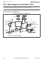
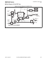
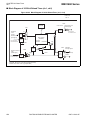
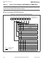
24.2 Block Diagrams of the Base Timer .................................................................................................... 656
24.3 Base Timer's Registers ...................................................................................................................... 664
24.4 Operations of the Base Timer ............................................................................................................ 675
24.5 32-bit Mode Operations ..................................................................................................................... 677
24.6 Notes of Using the Base Timer .......................................................................................................... 679
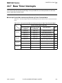
24.7 Base Timer Interrupts ........................................................................................................................ 681
24.8 Base Timer Description by Function Mode ........................................................................................ 682
24.8.1 PWM Function .............................................................................................................................. 683
24.8.2 PPG Function ............................................................................................................................... 697
24.8.3 Reload Timer Function ................................................................................................................. 712
24.8.4 PWC Function ............................................................................................................................... 724
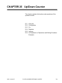
CHAPTER 25 Up/Down Counter ..................................................................................... 739
25.1 Overview ............................................................................................................................................ 740
25.2 Configuration ..................................................................................................................................... 742
25.3 Pin ...................................................................................................................................................... 744
25.4 Registers ............................................................................................................................................ 745
25.4.1 Reload Compare Register (RCR0 to RCR3) ................................................................................ 746
25.4.2 Up-Down Count Register (UDCR0 to UDCR3) ............................................................................. 748
25.4.3 Counter Control Register (CCR0 to CCR3) .................................................................................. 749
25.4.4 Counter Status Register (CSR0 to CSR3) .................................................................................... 754
25.5 Interrupt ............................................................................................................................................. 757
25.6 An Explanation of Operations and Setting Procedure Examples ....................................................... 759
25.6.1 Operation in Timer Mode .............................................................................................................. 763
25.6.2 Operations in Up/Down Count Mode ............................................................................................ 765
25.6.3 Operations in Phase Difference Count Mode (Multiplied by 2) ..................................................... 768
xiv
FUJITSU MICROELECTRONICS LIMITED
CM71-10146-1E
MB91660 Series
25.6.4 Operations in Phase Difference Count Mode (Multiplied by 4) ......................................................770
CHAPTER 26 10-Bit A/D Converter .................................................................................773
26.1 Overview .............................................................................................................................................774
26.2 Configuration ......................................................................................................................................775
26.3 Pins .....................................................................................................................................................777
26.4 Registers .............................................................................................................................................779
26.4.1 A/DC Control Registers (ADCR0) ..................................................................................................780
26.4.2 A/DC Status Registers (ADSR0) ...................................................................................................783
26.4.3 Scan Conversion Control Registers (SCCR0) ...............................................................................787
26.4.4 Scan Conversion FIFO Number Setting Register (SFNS0) ...........................................................791
26.4.5 Scan Conversion FIFO Data Registers (SCFD0) ..........................................................................793
26.4.6 Scan Conversion Input Select Registers (SCIS20 to SCIS00) ......................................................796
26.4.7 Priority Conversion Control Registers (PCCR0) ............................................................................798
26.4.8 Priority Conversion FIFO Number Setting Registers (PFNS0) ......................................................802
26.4.9 Priority Conversion FIFO Data Registers (PCFD0) .......................................................................804
26.4.10 Priority Conversion Input Select Registers (PCIS0) ......................................................................808
26.4.11 A/D Comparison Data Setting Registers (CMPD0) .......................................................................811
26.4.12 A/D Comparison Control Registers (CMPCR0) .............................................................................812
26.4.13 Sampling Time Setting Registers (ADST00, ADST10) ..................................................................816
26.4.14 Sampling Time Select Registers (ADSS20 to ADSS00) ...............................................................819
26.4.15 Compare Time Setting Registers (ADCT0) ...................................................................................820
26.5 Interrupts ............................................................................................................................................822
26.6 Explanation of Operations and Setting Procedure Examples .............................................................824
26.6.1 Operation of A/D Scan Conversion ...............................................................................................834
26.6.2 Operation of A/D Priority Conversion ............................................................................................837
26.6.3 FIFO Operations ............................................................................................................................840
26.6.4 Activating the DMA Controller (DMAC) .........................................................................................846
CHAPTER 27 8-bit D/A Converter ...................................................................................849
27.1 Overview .............................................................................................................................................850
27.2 Configuration ......................................................................................................................................851
27.3 Pins .....................................................................................................................................................853
27.4 Registers .............................................................................................................................................854
27.4.1 D/A Data Registers (DADR0 to DADR2) .......................................................................................855
27.4.2 D/A Control Registers (DACR0 to DACR2) ...................................................................................856
27.5 Explanation of Operations and Setting Procedure Examples .............................................................857
27.5.1 Operations of the 8-bit D/A Converter ...........................................................................................857
CHAPTER 28 Multi-function Serial Interface .................................................................859
28.1 Characteristics of Multi-function Serial Interface ................................................................................860
28.2 UART (Asynchronous Serial Interface) ...............................................................................................861
28.3 Overview of UART (Asynchronous Serial Interface) ...........................................................................862
28.4 Registers of UART (Asynchronous Serial Interface) ..........................................................................864
28.4.1 Serial Control Register (SCR) .......................................................................................................869
28.4.2 Serial Mode Register (SMR) ..........................................................................................................871
28.4.3 Serial Status Register (SSR) .........................................................................................................874
28.4.4 Extended Serial Control Register (ESCR) .....................................................................................877
28.4.5 Reception Data Register / Transmission Data Register (RDR/TDR) ............................................879
CM71-10146-1E
FUJITSU MICROELECTRONICS LIMITED
xv
MB91660 Series
28.4.6 Baud Rate Generator Registers 1, 0 (BGR1, BGR0) ................................................................... 882
28.4.7 FIFO Control Register 1 (FCR1) ................................................................................................... 884
28.4.8 FIFO Control Register 0 (FCR0) ................................................................................................... 886
28.4.9 FIFO Byte Register (FBYTE1/FBYTE2) ....................................................................................... 889
28.5 Interrupts of UART ............................................................................................................................. 891
28.5.1 Occurrence of Reception Interrupts and Flag Set Timing ............................................................. 893
28.5.2 Occurrence of Interrupts when Reception FIFO is Used and Flag Set Timing ............................. 894
28.5.3 Occurrence of Transmission Interrupts and Flag Set Timing ....................................................... 895
28.5.4 Occurrence of Interrupts when Transmission FIFO is Used and Flag Set Timing ........................ 896
28.6 Operation of UART ............................................................................................................................ 897
28.7 Dedicated Baud Rate Generator ....................................................................................................... 902
28.7.1 Setting Baud Rate ......................................................................................................................... 903
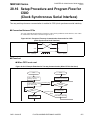
28.8 Setup Procedure and Program Flow for Operation Mode 0 (Asynchronous Normal Mode) .............. 907
28.9 Setup Procedure and Program Flow for Operation Mode 1 (Asynchronous Multi-processor Mode) . 909
28.10 CSIO (Clock Synchronous Serial Interface) ....................................................................................... 913
28.11 Overview of CSIO (Clock Synchronous Serial Interface) ................................................................... 914
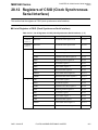
28.12 Registers of CSIO (Clock Synchronous Serial Interface) .................................................................. 915
28.12.1 Serial Control Register (SCR) ....................................................................................................... 921
28.12.2 Serial Mode Register (SMR) ......................................................................................................... 924
28.12.3 Serial Status Register (SSR) ........................................................................................................ 927
28.12.4 Extended Serial Control Register (ESCR) .................................................................................... 929
28.12.5 Reception Data Register / Transmission Data Register (RDR/TDR) ............................................ 931
28.12.6 Baud Rate Generator Registers 1, 0 (BGR1, BGR0) ................................................................... 934
28.12.7 FIFO Control Register 1 (FCR1) ................................................................................................... 935
28.12.8 FIFO Control Register 0 (FCR0) ................................................................................................... 937
28.12.9 FIFO Byte Register (FBYTE1/FBYTE2) ....................................................................................... 940
28.12.10Serial Mode Select Registers (SSEL0123, SSEL4567) .............................................................. 942
28.12.11Received Data Mirror Registers/Transmitted Data Mirror Registers (RDRM/TDRM) .................. 944
28.13 Interrupts of CSIO (Clock Synchronous Serial Interface) .................................................................. 945
28.13.1 Occurrence of Reception Interrupts and Flag Set Timing ............................................................. 947
28.13.2 Occurrence of Interrupts when Reception FIFO is Used and Flag Set Timing ............................. 948
28.13.3 Occurrence of Transmission Interrupts and Flag Set Timing ....................................................... 950
28.13.4 Occurrence of Interrupts when Transmission FIFO is Used and Flag Set Timing ........................ 951
28.14 Operation of CSIO (Clock Synchronous Serial Interface) .................................................................. 952
28.15 Dedicated Baud Rate Generator ....................................................................................................... 971
28.15.1 Setting Baud Rate ......................................................................................................................... 972
28.16 Setup Procedure and Program Flow for CSIO (Clock Synchronous Serial Interface) ....................... 975
28.17 I2C Interface ....................................................................................................................................... 977
28.18 Overview of I2C Interface ................................................................................................................... 978
28.19 Registers of I2C Interface .................................................................................................................. 979
28.19.1 I2C Bus Control Register (IBCR) .................................................................................................. 985
28.19.2 Serial Mode Register (SMR) ......................................................................................................... 990
28.19.3 I2C Bus Status Register (IBSR) .................................................................................................... 992
28.19.4 Serial Status Register (SSR) ........................................................................................................ 996
28.19.5 Reception Data Register / Transmission Data Register (RDR/TDR) ............................................ 998
28.19.6 7-bit Slave Address Mask Register (ISMK) ................................................................................ 1000
28.19.7 7-bit Slave Address Register (ISBA) ........................................................................................... 1001
28.19.8 Baud Rate Generator Registers 1, 0 (BGR1, BGR0) ................................................................. 1002
xvi
FUJITSU MICROELECTRONICS LIMITED
CM71-10146-1E
MB91660 Series
28.19.9 FIFO Control Register 1 (FCR1) ..................................................................................................1003
28.19.10FIFO Control Register 0 (FCR0) ................................................................................................1005
28.19.11FIFO Byte Register (FBYTE1/FBYTE2) .....................................................................................1009
28.20 Interrupts of I2C Interface .................................................................................................................1011
28.20.1 Operation of I2C Interface Communication ..................................................................................1013
28.20.2 Master Mode ................................................................................................................................1014
28.20.3 Slave Mode ..................................................................................................................................1031
28.20.4 Bus Error .....................................................................................................................................1035
28.21 Dedicated Baud Rate Generator ......................................................................................................1036
28.21.1 Example of I2C Flowcharts ..........................................................................................................1038
CHAPTER 29 USB Clock Generating Part ...................................................................1051
29.1 Overview ...........................................................................................................................................1052
29.2 Configuration ....................................................................................................................................1053
29.3 Registers ...........................................................................................................................................1054
29.3.1 USB Clock Configuration Register (UCCR) .................................................................................1055
29.4 Explanation of Operations and Setting Procedure Examples ...........................................................1057
CHAPTER 30 DMA Transfer Request Selector ............................................................1059
30.1 Overview ...........................................................................................................................................1060
30.2 Configuration ....................................................................................................................................1061
30.3 Registers ...........................................................................................................................................1062
30.3.1 DREQ Select Register (DREQSEL) ............................................................................................1063
CHAPTER 31 USB Function ..........................................................................................1065
31.1 Overview ...........................................................................................................................................1066
31.2 Configuration ....................................................................................................................................1067
31.3 Registers ...........................................................................................................................................1068
31.3.1 USB Selection Register (USBSEL) .............................................................................................1071
31.3.2 USB Enable Register (USBEN) ...................................................................................................1072
31.3.3 UDC Control Register (UDCC) ....................................................................................................1073
31.3.4 EP0 Control Register (EP0C) ......................................................................................................1077
31.3.5 EP1 to 5 Control Registers (EP1C to EP5C) ...............................................................................1079
31.3.6 Time Stamp Register (TMSP) .....................................................................................................1084
31.3.7 UDC Status Register (UDCS) ......................................................................................................1085
31.3.8 UDC Enable Interrupt Request Register (UDCIE) .......................................................................1089
31.3.9 EP0I Status Register (EP0IS) ......................................................................................................1091
31.3.10 EP0O Status Register (EP0OS) ..................................................................................................1093
31.3.11 EP1 to 5 Status Registers (EP1S to EP5S) .................................................................................1096
31.3.12 EP0 to 5 Data Registers (EP0DTH to EP5DTH/EP0DTL to EP5DTL) ........................................1100
31.4 Explanation of Operations and Setting Procedure Examples ...........................................................1102
31.4.1 Detection of Connections and Disconnections ............................................................................1105
31.4.2 Register Operation for a Command Response ...........................................................................1108
31.4.3 STALL Response and Release ...................................................................................................1110
31.4.4 Suspend Function ........................................................................................................................1114
31.4.5 Wakeup Function .........................................................................................................................1115
31.4.6 DMA Transfer Function ...............................................................................................................1117
31.4.7 NULL Transfer Function ..............................................................................................................1122
31.4.8 Software Control Examples .........................................................................................................1123
CM71-10146-1E
FUJITSU MICROELECTRONICS LIMITED
xvii
MB91660 Series
CHAPTER 32 USB Mini-HOST ...................................................................................... 1129
32.1 Overview .......................................................................................................................................... 1130
32.2 Configuration ................................................................................................................................... 1132
32.3 Registers .......................................................................................................................................... 1134
32.3.1 Host Control Register 0, 1 (HCNT) ............................................................................................. 1136
32.3.2 Host Interrupt Register (HIRQ) ................................................................................................... 1141
32.3.3 Host Error Status Register (HERR) ............................................................................................ 1145
32.3.4 Host Status Register (HSTATE) ................................................................................................. 1149
32.3.5 SOF Interrupt FRAME comparison register (HFCOMP) ............................................................. 1152
32.3.6 Retry Timer Setting Register (HRTIMER) ................................................................................... 1153
32.3.7 Host Address Register (HADR) .................................................................................................. 1155
32.3.8 EOF Setting Register (HEOF) .................................................................................................... 1156
32.3.9 FRAME Setting Register (HFRAME) .......................................................................................... 1158
32.3.10 Host Token Endpoint Register (HTOKEN) ................................................................................. 1160
32.4 Explanation of Operations and Setting Procedure Examples .......................................................... 1162
32.4.1 Connecting a USB Device .......................................................................................................... 1162
32.4.2 Resetting the USB Bus ............................................................................................................... 1164
32.4.3 Token Packets ............................................................................................................................ 1165
32.4.4 Data Packets .............................................................................................................................. 1166
32.4.5 Operation of a Handshake Packet .............................................................................................. 1167
32.4.6 Retry Function ............................................................................................................................ 1167
32.4.7 SOF Interrupts ............................................................................................................................ 1169
32.4.8 Error Status ................................................................................................................................. 1171
32.4.9 Packet End ................................................................................................................................. 1172
32.4.10 Suspend and Resume ................................................................................................................ 1173
32.4.11 Disconnecting a USB Device ...................................................................................................... 1175
32.5 Flowcharts for tokens in operation with USB Mini-HOST ................................................................ 1176
CHAPTER 33 DMA Controller (DMAC) ......................................................................... 1181
33.1 Overview .......................................................................................................................................... 1182
33.2 Configuration ................................................................................................................................... 1185
33.3 Pins .................................................................................................................................................. 1187
33.4 Registers .......................................................................................................................................... 1188
33.4.1 DMA Control Register (DMACR) ................................................................................................ 1190
33.4.2 DMA Source Address Registers (DSAR0 to DSAR7) ................................................................. 1193
33.4.3 DMA Destination Address Registers (DDAR0 to DDAR7) .......................................................... 1194
33.4.4 DMA Transfer Count Registers (DTCR0 to DTCR7) .................................................................. 1195
33.4.5 DMA Channel Control Registers (DCCR0 to DCCR7) ............................................................... 1196
33.4.6 DMA Channel Status Registers (DCSR0 to DCSR7) ................................................................. 1205
33.4.7 DMA-Halt by Interrupt Level Register (DILVR) ........................................................................... 1208
33.5 Interrupts .......................................................................................................................................... 1210
33.6 An Explanation of Operations and Setting Procedure Examples ..................................................... 1211
33.6.1 Transfer Settings ........................................................................................................................ 1211
33.6.2 Transfer Operations .................................................................................................................... 1214
33.6.3 Transfer Suspension ................................................................................................................... 1224
33.6.4 Operation at the End of Transfer ................................................................................................ 1226
33.6.5 Post-transfer Operation .............................................................................................................. 1227
33.6.6 DMA Transfer Halt ...................................................................................................................... 1231
xviii
FUJITSU MICROELECTRONICS LIMITED
CM71-10146-1E
MB91660 Series
CHAPTER 34 Select Function for DMA Transfer Request Generation/Clear by a
Peripheral Function ...............................................................................1233
34.1 Overview ...........................................................................................................................................1234
34.2 Configuration ....................................................................................................................................1235
34.3 Registers ...........................................................................................................................................1237
34.3.1 IO-Data Request Registers (IORR0 to IORR7) ...........................................................................1239
34.3.2 Select Register 0 for DMA Transfer Request Clear by a Peripheral Function (ICSEL0) .............1245
34.3.3 Select Register 1 for DMA Transfer Request Clear by a Peripheral Function (ICSEL1) .............1247
34.3.4 Select Register 2 for DMA Transfer Request Clear by a Peripheral Function (ICSEL2) .............1249
34.3.5 Select Register 3 for DMA Transfer Request Clear by a Peripheral Function (ICSEL3) .............1251
34.3.6 Select Register 4 for DMA Transfer Request Clear by a Peripheral Function (ICSEL4) .............1253
34.3.7 Select Register 5 for DMA Transfer Request Clear by a Peripheral Function (ICSEL5) .............1255
34.3.8 Select Register 6 for DMA Transfer Request Clear by a Peripheral Function (ICSEL6) .............1258
34.3.9 Select Register 7 for DMA Transfer Request Clear by a Peripheral Function (ICSEL7) .............1260
34.3.10 Select Register 8 for DMA Transfer Request Clear by a Peripheral Function (ICSEL8) .............1262
34.3.11 Select Register 9 for DMA Transfer Request Clear by a Peripheral Function (ICSEL9) .............1264
34.3.12 Select Register 10 for DMA Transfer Request Clear by a Peripheral Function (ICSEL10) .........1266
34.3.13 Select Register 11 for DMA Transfer Request Clear by a Peripheral Function (ICSEL11) .........1270
34.3.14 Select Register 12 for DMA Transfer Request Clear by a Peripheral Function (ICSEL12) .........1273
34.3.15 Select Register 13 for DMA Transfer Request Clear by a Peripheral Function (ICSEL13) .........1276
34.3.16 Select Register 14 for DMA Transfer Request Clear by a Peripheral Function (ICSEL14) .........1279
34.4 An Explanation of Operations and Setting Procedure Examples .....................................................1281
34.4.1 Operations upon a DMA Transfer ................................................................................................1281
CHAPTER 35 Control of Built-in Program Memory .....................................................1283
35.1 Overview of Built-in Program Memory Controller .............................................................................1284
35.2 Register for Built-in Program Memory Controller ..............................................................................1285
35.2.1 FLASH Control Register (FCTLR) ...............................................................................................1286
CHAPTER 36 Flash Memory ..........................................................................................1289
36.1 Overview of Flash Memory ...............................................................................................................1290
36.2 Flash Memory Configuration .............................................................................................................1291
36.3 Flash Memory Registers ...................................................................................................................1293
36.3.1 FLASH Status Register (FSTR) ...................................................................................................1294
36.3.2 FLASH Control Register (FCTLR) ...............................................................................................1295
36.4 Flash Memory Access Mode ............................................................................................................1296
36.5 Automatic Programming Algorithm ...................................................................................................1297
36.5.1 Command Sequence ...................................................................................................................1297
36.5.2 Execution State of Automatic Programming Algorithm ................................................................1300
36.6 Explanation of Flash Memory Operation ..........................................................................................1305
36.6.1 Read/Reset Operation .................................................................................................................1305
36.6.2 Write Operation ...........................................................................................................................1306
36.6.3 Chip Erase ...................................................................................................................................1309
36.6.4 Sector Erase ................................................................................................................................1309
36.6.5 Sector Erase Suspending ............................................................................................................1311
36.6.6 Sector Erase Restarting ..............................................................................................................1313
36.7 Notes on Using Flash Memory .........................................................................................................1314
CM71-10146-1E
FUJITSU MICROELECTRONICS LIMITED
xix
MB91660 Series
CHAPTER 37 Wild Register .......................................................................................... 1315
37.1 Overview of Wild Register ............................................................................................................... 1316
37.2 Configuration of Wild Register ......................................................................................................... 1317
37.3 Registers of Wild Register ............................................................................................................... 1318
37.3.1 Wild Register Address Register (WRAR00 to WRAR15) ........................................................... 1320
37.3.2 Wild Register Data Register (WRDR00 to WRDR15) ................................................................. 1321
37.3.3 Wild Register Enable Register (WREN) ..................................................................................... 1322
37.4 Explanation of Operations and Setting Procedure Examples of the Wild Register .......................... 1323
37.4.1 Wild Register Operation .............................................................................................................. 1323
37.5 Notes on Using the Wild Register .................................................................................................... 1324
CHAPTER 38 Serial Programming Connection .......................................................... 1327
38.1 Fujitsu Microelectronics Serial Programmer .................................................................................... 1328
38.1.1 Pins Used ................................................................................................................................... 1335
CHAPTER 39 Handling the Device ............................................................................... 1337
39.1 Notes on Handling the Device ......................................................................................................... 1338
APPENDIX A I/O Map .................................................................................................... 1346
APPENDIX B List of Registers ..................................................................................... 1370
APPENDIX C Interrupt Vectors .................................................................................... 1397
APPENDIX D Pin State in Each CPU State .................................................................. 1401
APPENDIX E
E.1
E.2
E.3
Lists of Instructions ............................................................................... 1415
Instruction List .................................................................................................................................. 1415
Instruction Tables ............................................................................................................................ 1419
List of Instructions That Can Be Specified for Delay Slots ............................................................... 1432
Index of Pins ..................................................................................................................... 1435
xx
FUJITSU MICROELECTRONICS LIMITED
CM71-10146-1E
Main changes in this edition
Page
-
Changes (For details, refer to main body.)
First edition
xxi
xxii
CHAPTER 1 Overview
This chapter explains the features and basic specifications
of the MB91660 series.
1.1
1.2
1.3
1.4
CM71-10146-1E
MB91660 Series Overview
MB91660 Series Product Configuration
MB91660 Series Block Diagram
Package Dimensions
FUJITSU MICROELECTRONICS LIMITED
1
CHAPTER 1 Overview
1.1
1.1
MB91660 Series
MB91660 Series Overview
The MB91660 series, a microcontroller that uses 32-bit RISC CPUs, has built-in peripheral control
functions for embedded control which requires high-performance/high-speed CPU processing.
This series is based on the FR80 family CPUs and is implemented in a single-chip.
■ FR80 family CPUs
•
32-bit RISC, load/store architecture, 5-stage pipeline
•
16 general-purpose 32-bit registers
•
16-bit fixed-length instructions (basic instructions), 1 instruction per cycle
•
Instructions suitable for embedded applications
-
Instructions for memory-to-memory transfer, bit processing, barrel shift, etc.
-
High-level language support instructions
Function entry/exit instructions and multi-load/store instructions for register contents
-
Bit search instruction
1 detection, 0 detection, and transition point detection
-
Branch instruction with delay slot(s)
-
Register interlock function
Reduced overhead time in branch executions
Efficient assembly language coding
-
Support for multipliers at the built-in function/instruction level
Signed 32-bit multiplication - 5 cycles
Signed 16-bit multiplication - 3 cycles
-
Interrupt (Save PC and PS)
High-speed response at a minimum of 6 cycles, 16 levels of priority
-
Simultaneous access to a program and data enabled by Harvard architecture
The prefetch function for instructions using the 4-word instruction queue in the CPU
•
2
Basic instruction compatibility with the FR family CPUs
-
Addition of the bit search instruction
-
No resource instruction and coprocessor instruction provided
CM71-10146-1E
CHAPTER 1 Overview
1.1
MB91660 Series
■ Maximum operating frequency
CPU
33 MHz
Peripheral
33 MHz
External bus
33 MHz
■ External bus interface
•
Maximum operating frequency: 33 MHz
•
24 addresses, 8/16-bit data I/O (split bus/multiplex bus)
•
Chip select output support for 4 separate areas that can be specified
A programmable auto wait cycle for each area occurs.
■ DMA controller (DMAC)
•
Number of channels: 8
•
Address space: 32 bits (4 GB)
•
Transfer mode: Block transfer/Burst transfer/Demand transfer
•
Address update: Increment/Decrement/Fix (increment/decrement value fixed to 1, 2, or 4)
•
Transfer size: 8 bits, 16 bits, and 32 bits
•
Block size: 1 to 16
•
Transfer count: 1 to 65,535 times
•
Transfer request:
-
Request by software
-
Interrupt request of a built-in peripheral function (a shared interrupt request or external interrupt
request)
-
Request by an external pin
•
Reload function: Reloading of all channels can be specified.
•
Level of priority: Fixed (ch.0 > ch.1 > ch.2 > ch.3 > ...), or round robin
•
Interrupt request: Occurrence of a normal end interrupt request, abnormal end interrupt request, or
transfer suspension interrupt request
CM71-10146-1E
FUJITSU MICROELECTRONICS LIMITED
3
CHAPTER 1 Overview
1.1
MB91660 Series
■ Multifunction serial interface
•
4 channels with 16-byte FIFO, 8 channels without FIFO
•
Any of the following uses can be selected for each channel (For ch.0, I2C is not available.):
-
UART
-
CSIO
-
I2C
[Features of UART]
-
Full-duplex double buffer
-
Selection with or without parity supported
-
Built-in dedicated baud rate generator
-
External clock available as a serial clock
-
Various error detection functions available (parity errors, framing errors, and overrun errors)
[Features of CSIO]
-
Full-duplex double buffer
-
Built-in dedicated baud rate generator
-
Overrun error detection function available
[Features of I2C]
-
Standard mode (maximum: 100 kbps)/High-speed mode (maximum: 400 kbps) supported
-
5V tolerance supported for some channels
■ Interrupts
•
Total of 32 external interrupts (5V tolerance supported for some pins)
•
Interrupt from an internal peripheral function
•
Programmable setting of interrupt levels (16 levels)
•
Return from stop mode or sleep mode supported
■ A/D converter
4
•
24 channels, 1 unit
•
10-bit resolution
•
Successive comparison type Conversion time: Approximately 1.2 µs (PCLK=33 MHz)
•
Priority A/D conversion available (2 levels)
•
Conversion mode (one shot conversion mode, scanning conversion mode)
•
Activation trigger (software/external trigger/base timer)
•
FIFO for storing conversion data available (scanning conversion: 16 levels; priority conversion: 4
levels)
CM71-10146-1E
CHAPTER 1 Overview
1.1
MB91660 Series
■ D/A converter
•
•
Number of channels: 3 built-in channels
8-bit resolution
■ Base timer
•
•
•
•
•
Number of channels: 16 built-in channels
Any of the following uses can be selected for each channel:
- 16/32-bit reload timer
- 16-bit PWM timer
- 16/32-bit PWC timer
- 16-bit PPG timer
32-bit timer available by connecting 2 channels in cascade
Function for activating multiple channels simultaneously available
I/O select function available
■ 16-bit reload timer
•
•
•
Number of channels: 3 (including a channel for REALOS)
Interval timer function
Function for selecting count clock (Peripheral clock (PCLK) divided by a value ranging from 2 to 64)
■ Compare timer
•
•
•
32-bit input capture: 8 built-in channels
32-bit output compare: 8 built-in channels
32-bit free-run timer: 2 built-in channels
■ Other interval timers
•
•
•
Up/Down counter: 4 built-in channels
Watch counter: 1 built-in channel
Watchdog timer: 1 built-in channel
■ USB function with Mini-HOST
•
•
•
•
Number of channels: 1
Supports Full-Speed only
The USB function and USB Mini-HOST are the switch types (USB I/O multiplexed)
Support of DMA transfer
[USB Function]
•
•
Support of up to six endpoints
- Endpoint 0 is provided for the fixed use of control transfers
- Bulk or interrupt transfer can be selected for endpoint 1 to 5
Double buffer structure for endpoint 1 to 5
[USB Mini-HOST]
•
•
•
•
•
CM71-10146-1E
Support of bulk and interrupt transfer (Only using endpoint1 and endpoint2)
Automatic detection of connection/disconnection of USB devices
Automatic processing of a handshake packet for IN/OUT token processing
Support of a maximum packet length of up to 256 bytes
Support for a wakeup function
FUJITSU MICROELECTRONICS LIMITED
5
CHAPTER 1 Overview
1.1
MB91660 Series
■ Slave interface
•
Equipped with a register for communication along with large-capacity transmission/ reception FIFO
that enables large amount of data transmission and reception.
•
Buffer: reception 1.5 Kbytes, transmission 1.5 Kbytes
•
Host function: A function to process by storing to a buffer. Once the buffer is full, this function stops
data reception. Communication control is possible during data transmission/ reception. This enables
CPU load reduction and efficiency of communication.
•
16-bit data port
•
Transmission/ reception data port control function
■ Main timer
•
Number of channels: 1
•
Count of the oscillation stabilization wait time of the main clock (MCLK).
•
Count of the oscillation stabilization wait time of the PLL clock (PLLCLK).
•
Interval timer when the oscillation of the main clock (MCLK) is stable.
•
Number of channels: 1
•
Count of the oscillation stabilization wait time of the sub clock (SBCLK).
•
Interval timer when the oscillation of the sub clock (SBCLK) is stable.
■ Sub timer
■ Clock generation
•
Main clock (MCLK) oscillation
•
Sub clock (SBCLK) oscillation
•
PLL clock (PLLCLK) oscillation
■ Low-power dissipation mode
•
Stop mode
•
Watch mode
•
Sleep mode
•
Doze mode
•
Clock division function
■ Other features
•
I/O port
•
INIT pin available as a reset pin.
•
Watchdog timer reset and software reset available
•
Delay interrupt
•
Power supply
-
6
Single power supply (When USB not used: 2.7 V to 3.6 V, When USB used: 3.0 V to 3.6 V)
CM71-10146-1E
CHAPTER 1 Overview
1.2
MB91660 Series
1.2
MB91660 Series Product Configuration
This section explains the products in the MB91660 series.
Table 1.2-1 MB91660 series product configuration (1 / 2)
Part number
MB91V650
MB91F662
MB91661
MB91664
Evaluation product
Flash memory
product
Built-in program
memory capacity
(Support by
emulation
memory)
512 Kbytes
(Flash)
384 Kbytes
(ROM)
128 Kbytes
(ROM)
Built-in RAM capacity
128 Kbytes
48 Kbytes
32 Kbytes
16 Kbytes
Parameter
Product type
External bus interface
Yes
DMA controller
(DMAC)
8 channels
Base timer
16 channels
Multifunction serial
interface
Without FIFO : 8 channels (ch.0 to ch.7)
With FIFO : 4 channels (ch.8 to ch.11)
External interrupt
32 (some pins are 5 V tolerant)
10-bit A/D converter
32 channels
(2 units)
24 channels (1 unit)
8-bit D/A converter
3 channels
16-bit reload timer
3 channels
Compare timer
32-bit input capture : 8 channels
32-bit output compare : 8 channels
32-bit free-run timer : 2 channels
Up/Down counter
4 channels
Watch counter
1 channel
I/O port
USB function with
Mini-HOST
Slave interface
154
99
1 channel
Yes
Main timer
1 channel
Sub timer
1 channel
Wild register
CM71-10146-1E
MASK ROM product
16 channels
FUJITSU MICROELECTRONICS LIMITED
7
CHAPTER 1 Overview
1.2
MB91660 Series
Table 1.2-1 MB91660 series product configuration (2 / 2)
Part number
MB91V650
MB91F662
MB91661
MB91664
Parameter
Debug function
Package
8
DSU4
-
-
Type: LQFP-120
Package code: FPT-120P-M21
Pin pitch: 0.50mm
Size:16.0mm × 16.0mm
CM71-10146-1E
CHAPTER 1 Overview
1.3
MB91660 Series
1.3
MB91660 Series Block Diagram
Figure 1.3-1 is the block diagrams of the MB91660 series.
Figure 1.3-1 MB91660 series block diagram
Step-down regulator
FR80
CPU
Built-in program
memory
Flash memory /
Mask ROM
Cross bar
switch
RAM
On-chip bus
DMAC
8 channels
Peripheral bus
bridge
Watchdog timer
Interrupt controller
Delay interrupt
USB function with
Mini-HOST
Clock generation
USB clock
generation
Slave
interface
Watch counter
16 -bit reload timer
3 channels
32-bit free-run timer
2channels
Base timer
16 channels
Up/down counter
4 channels
32-bit input capture
8 channels
A/D converter
24 channels (1 unit)
32-bit output compare
8 channels
D/A converter
3 channels
Multi-function serial interface
8 channels
Port
Port
External interrupt
32 channels
16 -bit peripheral bus
Clock control
32 -bit peripheral bus
External bus I/F
Multi-function serial interface
with FIFO 4 channels
Port
CM71-10146-1E
FUJITSU MICROELECTRONICS LIMITED
9
CHAPTER 1 Overview
1.4
1.4
MB91660 Series
Package Dimensions
The dimensions of the packages used for the MB91660 series are shown below.
Figure 1.4-1 Package dimensions (FPT-120P-M21)
120-pin plastic LQFP
Lead pitch
0.50 mm
Package width ×
package length
16.0 × 16.0 mm
Lead shape
Gullwing
Sealing method
Plastic mold
Mounting height
1.70 mm MAX
Weight
0.88 g
(FPT-120P-M21)
120-pin plastic LQFP
(FPT-120P-M21)
18.00±0.20(.709±.008)SQ
16.00±0.10(.630±.004)SQ
90
61
91
60
0.08(.003)
Details of "A" part
+0.20
1.50 –0.10
+.008
(Mounting height)
.059 –.004
INDEX
0~8°
120
LEAD No.
1
30
0.50(.020)
C
"A"
31
0.22±0.05
(.009±.002)
2001-2008 FUJITSU MICROELECTRONICS LIMITED F120033S-c-3-4
0.08(.003)
M
0.145
.006
+0.05
–0.03
+.002
–.001
0.60±0.15
(.024±.006)
0.10±0.05
(.004±.002)
(Stand off)
0.25(.010)
Dimensions in mm (inches).
Note: The values in parentheses are reference values.
For the latest specifications of package dimensions, refer to the following URL.
http://edevice.fujitsu.com/package/en-search/
10
CM71-10146-1E
CHAPTER 2 Pins of the MB91660 Series
This chapter explains the pins and multiplexed pin settings
of the MB91660 series.
2.1
2.2
2.3
2.4
CM71-10146-1E
Pin Assignment Diagram
Pin Functions
I/O Circuit Types
Setting Method for Pins
FUJITSU MICROELECTRONICS LIMITED
11
CHAPTER 2 Pins of the MB91660 Series
2.1
2.1
MB91660 Series
Pin Assignment Diagram
1 type of package is available for the MB91660 series.
■ LQFP-120
Figure 2.1-1 Pin assignment diagram in the LQFP-120 series
P15/D13/TIOB6/SIN3/BIN1/INT5
P14/D12/TIOA6/SOUT3/AIN1/INT4
P13/D11/TIOB5/INT3
P12/D10/TIOA5/SCK2/ZIN0/INT2
P11/D09/TIOB4/SIN2/BIN0/INT1
P10/D08/TIOA4/SOUT2/AIN0/INT0
P07/D07/TIOB3/IN7
P06/D06/TIOA3/SCK1/IN6
VCC
97
96
95
94
93
92
91
P16/D14/TIOA7/SCK3/ZIN1/INT6
98
P17/D15/TIOB7/INT7
100
99
P20/A00/TIOA8/SOUT4/AIN2
101
P26/A06/TIOA11/SCK5/ZIN3/OUT2/SIFD4_1
108
P21/A01/TIOB8/SIN4/BIN2
P27/A07/TIOB11/OUT3/SIFD5_1
109
P22/A02/TIOA9/SCK4/ZIN2/SIFD0_1
P30/A08/TIOA12/SOUT6/INT8/SIFD6_1
110
102
P31/A09/TIOB12/SIN6/INT9/SIFD7_1
111
103
P32/A10/TIOA13/SCK6/INT10/SIFD8_1
112
104
P33/A11/TIOB13/INT11/SIFD9_1
113
P25/A05/TIOB10/SIN5/BIN3/OUT1/SIFD3_1
P34/A12/TIOA14/SOUT7/OUT4/INT12/SIFD10_1
114
P23/A03/TIOB9/SIFD1_1
P35/A13/TIOB14/SIN7/OUT5/INT13/SIFD11_1
115
105
P36/A14/TIOA15/SCK7/OUT6/INT14/SIFD12_1
116
P24/A04/TIOA10/SOUT5/AIN3/OUT0/SIFD2_1
P37/A15/TIOB15/OUT7/INT15/SIFD13_1
117
106
P40/A16/SOUT8/SIFD14_1
118
107
VCC
P41/A17/SIN8/SIFD15_1
119
1
2
3
4
5
6
7
8
9
10
11
12
13
14
15
16
17
18
19
20
21
22
23
24
25
26
27
28
29
30
90
89
88
87
86
85
84
83
82
81
80
79
78
77
76
75
74
73
72
71
70
69
68
67
66
65
64
63
62
61
49
50
51
52
53
54
55
56
57
58
59
60
PA7/AN23/TMI2_1/INT23_1/SIFDRQT
AVCC
AVRH
AVSS
P90/DA0
P91/DA1
P92/DA2
PK3/ADTRG0_3
PK2/ADTRG0_2
PK1/X0A
PK0/X1A
47
PA4/AN20/TMO2_1/INT20_1/SIFWR
48
46
PA3/AN19/TMO1_1/INT19_1/SIFA
PA5/AN21/TMI0_1/INT21_1/SIFRD
45
PA6/AN22/TMI1_1/INT22_1/SIFDRQR
44
43
PA0/AN16/INT16_1/SIFD14
PA1/AN17/INT17_1/SIFD15
42
P87/AN15/IN7_1/INT31/SIFD13
PA2/AN18/TMO0_1/INT18_1/SIFCS
41
P86/AN14/IN6_1/INT30/SIFD12
37
P82/AN10/IN2_1/INT26/SIFD8
40
36
P81/AN9/IN1_1/INT25/SIFD7
P85/AN13/IN5_1/INT29/SIFD11
35
P80/AN8/IN0_1/INT24/SIFD6
39
34
P77/AN7/SCK0/TMI2/OUT7_1/INT23/SIFD5
38
33
P83/AN11/IN3_1/INT27/SIFD9
32
P84/AN12/IN4_1/INT28/SIFD10
31
VCC
P76/AN6/SIN0/TMI1/OUT6_1/INT22/SIFD4
LQFP-120
P75/AN5/SOUT0/TMI0/OUT5_1/INT21/SIFD3
VSS
C
P42/A18/SCK8/SIFCS_1
P43/A19/SIFA_1
P44/A20/SOUT9/SIFWR_1
P45/A21/SIN9/SIFRD_1
P46/A22/SCK9/SIFDRQR_1
P47/A23/SIFDRQT_1
PH0/TIOA4_1/SOUT2_1/AIN0_2/INT0_1
PH1/TIOB4_1/SIN2_1/BIN0_2/INT1_1
PH2/TIOA5_1/SCK2_1/ZIN0_2/INT2_1
PH3/TIOB5_1/INT3_1
VSS
UDP
UDM
VCC
PG0/DREQ2/TIOA0_1/SOUT0_2/IN0_2
PG1/DACK2/TIOB0_1/SIN0_2/IN1_2
PG2/DEOP2/TIOA1_1/SCK0_2/IN2_2
PG3/DREQ3/TIOB1_1/IN3_2
PG4/DACK3/TIOA2_1/SOUT1_1/IN4_2
PG5/DEOP3/TIOB2_1/SIN1_1/IN5_2
PG6/TIOA3_1/SCK1_1/IN6_2
PG7/TIOB3_1/IN7_2
P70/AN0/OUT0_1/INT16
P71/AN1/OUT1_1/INT17
P72/AN2/TMO0/OUT2_1/INT18/SIFD0
P73/AN3/TMO1/OUT3_1/INT19/SIFD1
P74/AN4/TMO2/OUT4_1/INT20/SIFD2
VSS
120
(TOP VIEW)
VSS
P05/D05/TIOB2/SIN1/IN5
P04/D04/TIOA2/SOUT1/IN4
P03/D03/TIOB1/IN3
P02/D02/TIOA1/SCK0_1/IN2
P01/D01/TIOB0/SIN0_1/IN1
P00/D00/TIOA0/SOUT0_1/IN0
P67/DEOP1/INT23_2
P66/DACK1/ZIN3_1/FRCK0_1
P65/DREQ1/BIN3_1/ADTRG0_1
P64/DEOP0/AIN3_1
P63/DACK0/FRCK1_1/INT22_2
P62/DREQ0/ZIN2_1
P61/SYSCLK/BIN2_1
P60/RDY/AIN2_1
P57/WR1
P56/WR0/SCK11/ZIN1_1/FRCK0
P55/RD/SIN11/BIN1_1/ADTRG0
P54/AS/SOUT11/AIN1_1
P53/CS3/FRCK1/INT21_2
P52/CS2/SCK10/ZIN0_1
P51/CS1/SIN10/BIN0_1
P50/CS0/SOUT10/AIN0_1
VCC
INIT
MD1
MD0
X1
X0
VSS
(FPT-120P-M21)
Note : The number after the underscore (“_”) in pin names such as XXX_1 and XXX_2 indicates the port number.
For these pins, there are multiple pins that provide the same function for the same channel. Use the extended port
function register (EPFR) to select the pin.
12
CM71-10146-1E
CHAPTER 2 Pins of the MB91660 Series
2.2
MB91660 Series
2.2
Pin Functions
Table 2.2-1 lists the pin functions of the MB91660 series.
In a pin that includes an underscore (_), such as XXX_1 and XXX_2, the number following the
underscore represents a port number. For details of the port numbers, see "2.4 Setting Method for
Pins".
■ Pin function list
Table 2.2-1 Pin functions (1 / 25)
Pin
Number
I/O
Circuit
Type*1
Function
CMOS
level
input
CMOS
level
hysteres
is input
1
VSS
-
GND pin
-
-
2
C
-
Power stabilization capacity pin
-
-
3
P42
General-purpose I/O port
-
❍
A18
External bus interface address bus bit18
-
-
SCK8
(SCL8)
Multifunction serial interface ch.8
clock I/O pin.
This pin operates as SCK8 when it is
used in a UART/CSIO (operation
modes 0 to 2) and as SCL8 when it is
used in an I2C (operation mode 4).
-
❍
SIFCS_1
Slave interface chip select signal input
pin (Port 1)
❍
-
General-purpose I/O port
-
❍
A19
External bus interface address bus bit19
-
-
SIFA_1
Slave interface address signal input pin
(Port 1)
❍
-
General-purpose I/O port
-
❍
A20
External bus interface address bus bit20
-
-
SOUT9
(SDA9)
Multifunction serial interface ch.9
output pin.
This pin operates as SOUT9 when it is
used in a UART/CSIO (operation
modes 0 to 2) and as SDA9 when it is
used in an I2C (operation mode 4).
-
❍
SIFWR_1
Slave interface write strobe signal input
pin (Port 1)
❍
-
4
5
CM71-10146-1E
Pin Name
Q*2
Q*2
P43
Q*2
P44
FUJITSU MICROELECTRONICS LIMITED
13
CHAPTER 2 Pins of the MB91660 Series
2.2
MB91660 Series
Table 2.2-1 Pin functions (2 / 25)
Pin
Number
6
7
8
9
14
CMOS
level
input
CMOS
level
hysteres
is input
General-purpose I/O port
-
❍
A21
External bus interface address bus bit21
-
-
SIN9
Multifunction serial interface ch.9 input
pin
-
❍
SIFRD_1
Slave interface read strobe signal input
pin (Port 1)
❍
-
General-purpose I/O port
-
❍
A22
External bus interface address bus bit22
-
-
SCK9
(SCL9)
Multifunction serial interface ch.9
clock I/O pin.
This pin operates as SCK9 when it is
used in a UART/CSIO (operation
modes 0 to 2) and as SCL9 when it is
used in an I2C (operation mode 4).
-
❍
SIFDRQR_1
Slave interface received data request
signal output pin (Port 1)
-
-
General-purpose I/O port
-
❍
A23
External bus interface address bus bit23
-
-
SIFDRQT_1
Slave interface transmitted data request
signal output pin (Port 1)
-
-
General-purpose I/O port
-
❍
TIOA4_1
Base timer ch.4 TIOA pin (Port 1)
-
❍
SOUT2_1
(SDA2_1)
Multifunction serial interface ch.2
output pin (Port 1).
This pin operates as SOUT2_1 when it
is used in a UART/CSIO (operation
modes 0 to 2) and as SDA2_1 when it is
used in an I2C (operation mode 4).
-
❍
AIN0_2
Up/Down counter ch.0 AIN input pin
(Port 2)
-
❍
INT0_1
External interrupt request 0 input pin
(Port 1)
-
❍
Pin Name
P45
P46
P47
PH0
I/O
Circuit
Type*1
Q*2
D*2
D*2
D*2
Function
CM71-10146-1E
CHAPTER 2 Pins of the MB91660 Series
2.2
MB91660 Series
Table 2.2-1 Pin functions (3 / 25)
Pin
Number
10
11
12
CM71-10146-1E
Pin Name
I/O
Circuit
Type*1
CMOS
level
input
CMOS
level
hysteres
is input
General-purpose I/O port
-
❍
TIOB4_1
Base timer ch.4 TIOB pin (Port 1)
-
❍
SIN2_1
Multifunction serial interface ch.2 input
pin (Port 1)
-
❍
BIN0_2
Up/Down counter ch.0 BIN input pin
(Port 2)
-
❍
INT1_1
External interrupt request 1 input pin
(Port 1)
-
❍
General-purpose I/O port
-
❍
TIOA5_1
Base timer ch.5 TIOA pin (Port 1)
-
❍
SCK2_1
(SCL2_1)
Multifunction serial interface ch.2
clock I/O pin (Port 1).
This pin operates as SCK2_1 when it is
used in a UART/CSIO (operation
modes 0 to 2) and as SCL2_1 when it is
used in an I2C (operation mode 4).
-
❍
ZIN0_2
Up/Down counter ch.0 ZIN input pin
(Port 2)
-
❍
INT2_1
External interrupt request 2 input pin
(Port 1)
-
❍
General-purpose I/O port
-
❍
TIOB5_1
Base timer ch.5 TIOB pin (Port 1)
-
❍
INT3_1
External interrupt request 3 input pin
(Port 1)
-
❍
GND pin
-
-
PH1
D*2
PH2
D*2
PH3
D*2
Function
13
VSS
-
14
UDP
USB
D+ pin of USB function in Mini-HOST
-
-
15
UDM
USB
D- pin of USB function in Mini-HOST
-
-
16
VCC
-
Power pin
-
-
FUJITSU MICROELECTRONICS LIMITED
15
CHAPTER 2 Pins of the MB91660 Series
2.2
MB91660 Series
Table 2.2-1 Pin functions (4 / 25)
Pin
Number
17
18
19
20
16
Pin Name
I/O
Circuit
Type*1
CMOS
level
input
CMOS
level
hysteres
is input
General-purpose I/O port
-
❍
DREQ2
DMA controller (DMAC) ch.2 transfer
request input pin
-
❍
TIOA0_1
Base timer ch.0 TIOA pin (Port 1)
-
❍
SOUT0_2
Multifunction serial interface ch.0
output pin (Port 2).
This pin operates as SOUT0_2 when it
is used in a UART/CSIO (operation
modes 0 to 2).
-
-
IN0_2
32-bit input capture ch.0 input pin (Port
2)
-
❍
General-purpose I/O port
-
❍
DACK2
DMA controller (DMAC) ch.2 transfer
request acceptance signal output pin
-
-
TIOB0_1
Base timer ch.0 TIOB pin (Port 1)
-
❍
SIN0_2
Multifunction serial interface ch.0 input
pin (Port 2)
-
❍
IN1_2
32-bit input capture ch.1 input pin (Port
2)
-
❍
General-purpose I/O port
-
❍
DEOP2
DMA controller (DMAC) ch.2 last
transfer signal output pin
-
-
TIOA1_1
Base timer ch.1 TIOA pin (Port 1)
-
❍
SCK0_2
Multifunction serial interface ch.0
clock I/O pin (Port 2).
This pin operates as SCK0_2 when it is
used in a UART/CSIO (operation
modes 0 to 2).
-
❍
IN2_2
32-bit input capture ch.2 input pin (Port
2)
-
❍
General-purpose I/O port
-
❍
DREQ3
DMA controller (DMAC) ch.3 transfer
request input pin
-
❍
TIOB1_1
Base timer ch.1 TIOB pin (Port 1)
-
❍
IN3_2
32-bit input capture ch.3 input pin (Port
2)
-
❍
PG0
PG1
PG2
PG3
D*2
D*2
D*2
D*2
Function
CM71-10146-1E
CHAPTER 2 Pins of the MB91660 Series
2.2
MB91660 Series
Table 2.2-1 Pin functions (5 / 25)
Pin
Number
21
22
23
24
CM71-10146-1E
Pin Name
I/O
Circuit
Type*1
CMOS
level
input
CMOS
level
hysteres
is input
General-purpose I/O port
-
❍
DACK3
DMA controller (DMAC) ch.3 transfer
request acceptance signal output pin
-
-
TIOA2_1
Base timer ch.2 TIOA pin (Port 1)
-
❍
SOUT1_1
(SDA1_1)
Multifunction serial interface ch.1
output pin (Port 1).
This pin operates as SOUT1_1 when it
is used in a UART/CSIO (operation
modes 0 to 2) and as SDA1_1 when it is
used in an I2C (operation mode 4).
-
❍
IN4_2
32-bit input capture ch.4 input pin (Port
2)
-
❍
General-purpose I/O port
-
❍
DEOP3
DMA controller (DMAC) ch.3 last
transfer signal output pin
-
-
TIOB2_1
Base timer ch.2 TIOB pin (Port 1)
-
❍
SIN1_1
Multifunction serial interface ch.1 input
pin (Port 1)
-
❍
IN5_2
32-bit input capture ch.5 input pin (Port
2)
-
❍
General-purpose I/O port
-
❍
TIOA3_1
Base timer ch.3 TIOA pin (Port 1)
-
❍
SCK1_1
(SCL1_1)
Multifunction serial interface ch.1
clock I/O pin (Port 1).
This pin operates as SCK1_1 when it is
used in a UART/CSIO (operation
modes 0 to 2) and as SCL1_1 when it is
used in an I2C (operation mode 4).
-
❍
IN6_2
32-bit input capture ch.6 input pin (Port
2)
-
❍
General-purpose I/O port
-
❍
TIOB3_1
Base timer ch.3 TIOB pin (Port 1)
-
❍
IN7_2
32-bit input capture ch.7 input pin (Port
2)
-
❍
PG4
D*2
D*2
PG5
PG6
D*2
PG7
D*2
Function
FUJITSU MICROELECTRONICS LIMITED
17
CHAPTER 2 Pins of the MB91660 Series
2.2
MB91660 Series
Table 2.2-1 Pin functions (6 / 25)
Pin
Number
25
26
27
28
18
Pin Name
I/O
Circuit
Type*1
CMOS
level
input
CMOS
level
hysteres
is input
General-purpose I/O port
-
❍
AN0
10-bit A/D converter ch.0 analog input
pin
-
-
OUT0_1
32-bit output compare ch.0 output pin
(Port 1)
-
-
INT16
External interrupt request 16 input pin
-
❍
General-purpose I/O port
-
❍
AN1
10-bit A/D converter ch.1 analog input
pin
-
-
OUT1_1
32-bit output compare ch.1 output pin
(Port 1)
-
-
INT17
External interrupt request 17 input pin
-
❍
General-purpose I/O port
-
❍
AN2
10-bit A/D converter ch.2 analog input
pin
-
-
TMO0
16-bit reload timer ch.0 output pin
-
-
OUT2_1
32-bit output compare ch.2 output pin
(Port 1)
-
-
INT18
External interrupt request 18 input pin
-
❍
SIFD0
Slave interface data I/O pin bit0
❍
-
General-purpose I/O port
-
❍
AN3
10-bit A/D converter ch.3 analog input
pin
-
-
TMO1
16-bit reload timer ch.1 output pin
-
-
OUT3_1
32-bit output compare ch.3 output pin
(Port 1)
-
-
INT19
External interrupt request 19 input pin
-
❍
SIFD1
Slave interface data I/O pin bit1
❍
-
P70
P71
P72
P73
E
E
R
R
Function
CM71-10146-1E
CHAPTER 2 Pins of the MB91660 Series
2.2
MB91660 Series
Table 2.2-1 Pin functions (7 / 25)
Pin
Number
29
I/O
Circuit
Type*1
CMOS
level
input
CMOS
level
hysteres
is input
General-purpose I/O port
-
❍
AN4
10-bit A/D converter ch.4 analog input
pin
-
-
TMO2
16-bit reload timer ch.2 output pin
-
-
OUT4_1
32-bit output compare ch.4 output pin
(Port 1)
-
-
INT20
External interrupt request 20 input pin
-
❍
SIFD2
Slave interface data I/O pin bit2
❍
-
P74
R
Function
30
VSS
-
GND pin
-
-
31
VCC
-
Power pin
-
-
32
P75
R
General-purpose I/O port
-
❍
AN5
10-bit A/D converter ch.5 analog input
pin
-
-
SOUT0
Multifunction serial interface ch.0
output pin.
This pin operates as SOUT0 when it is
used in a UART/CSIO (operation
modes 0 to 2).
-
-
TMI0
16-bit reload timer ch.0 input pin
-
❍
OUT5_1
32-bit output compare ch.5 output pin
(Port 1)
-
-
INT21
External interrupt request 21 input pin
-
❍
SIFD3
Slave interface data I/O pin bit3
❍
-
General-purpose I/O port
-
❍
AN6
10-bit A/D converter ch.6 analog input
pin
-
-
SIN0
Multifunction serial interface ch.0 input
pin
-
❍
TMI1
16-bit reload timer ch.1 input pin
-
❍
OUT6_1
32-bit output compare ch.6 output pin
(Port 1)
-
-
INT22
External interrupt request 22 input pin
-
❍
SIFD4
Slave interface data I/O pin bit4
❍
-
33
CM71-10146-1E
Pin Name
P76
R
FUJITSU MICROELECTRONICS LIMITED
19
CHAPTER 2 Pins of the MB91660 Series
2.2
MB91660 Series
Table 2.2-1 Pin functions (8 / 25)
Pin
Number
34
35
36
37
20
Pin Name
I/O
Circuit
Type*1
CMOS
level
input
CMOS
level
hysteres
is input
General-purpose I/O port
-
❍
AN7
10-bit A/D converter ch.7 analog input
pin
-
-
SCK0
Multifunction serial interface ch.0
clock I/O pin
This pin operates as SCK0 when it is
used in a UART/CSIO (operation
modes 0 to 2).
-
❍
TMI2
16-bit reload timer ch.2 input pin
-
❍
OUT7_1
32-bit output compare ch.7 output pin
(Port 1)
-
-
INT23
External interrupt request 23 input pin
-
❍
SIFD5
Slave interface data I/O pin bit5
❍
-
General-purpose I/O port
-
❍
AN8
10-bit A/D converter ch.8 analog input
pin
-
-
IN0_1
32-bit input capture ch.0 input pin (Port
1)
-
❍
INT24
External interrupt request 24 input pin
-
❍
SIFD6
Slave interface data I/O pin bit6
❍
-
General-purpose I/O port
-
❍
AN9
10-bit A/D converter ch.9 analog input
pin
-
-
IN1_1
32-bit input capture ch.1 input pin (Port
1)
-
❍
INT25
External interrupt request 25 input pin
-
❍
SIFD7
Slave interface data I/O pin bit7
❍
-
General-purpose I/O port
-
❍
AN10
10-bit A/D converter ch.10 analog input
pin
-
-
IN2_1
32-bit input capture ch.2 input pin (Port
1)
-
❍
INT26
External interrupt request 26 input pin
-
❍
SIFD8
Slave interface data I/O pin bit8
❍
-
P77
P80
P81
P82
R
R
R
R
Function
CM71-10146-1E
CHAPTER 2 Pins of the MB91660 Series
2.2
MB91660 Series
Table 2.2-1 Pin functions (9 / 25)
Pin
Number
38
39
40
41
CM71-10146-1E
Pin Name
I/O
Circuit
Type*1
CMOS
level
input
CMOS
level
hysteres
is input
General-purpose I/O port
-
❍
AN11
10-bit A/D converter ch.11 analog input
pin
-
-
IN3_1
32-bit input capture ch.3 input pin (Port
1)
-
❍
INT27
External interrupt request 27 input pin
-
❍
SIFD9
Slave interface data I/O pin bit9
❍
-
General-purpose I/O port
-
❍
AN12
10-bit A/D converter ch.12 analog input
pin
-
-
IN4_1
32-bit input capture ch.4 input pin (Port
1)
-
❍
INT28
External interrupt request 28 input pin
-
❍
SIFD10
Slave interface data I/O pin bit10
❍
-
General-purpose I/O port
-
❍
AN13
10-bit A/D converter ch.13 analog input
pin
-
-
IN5_1
32-bit input capture ch.5 input pin (Port
1)
-
❍
INT29
External interrupt request 29 input pin
-
❍
SIFD11
Slave interface data I/O pin bit11
❍
-
General-purpose I/O port
-
❍
AN14
10-bit A/D converter ch.14 analog input
pin
-
-
IN6_1
32-bit input capture ch.6 input pin (Port
1)
-
❍
INT30
External interrupt request 30 input pin
-
❍
SIFD12
Slave interface data I/O pin bit12
❍
-
P83
R
P84
R
P85
R
P86
R
Function
FUJITSU MICROELECTRONICS LIMITED
21
CHAPTER 2 Pins of the MB91660 Series
2.2
MB91660 Series
Table 2.2-1 Pin functions (10 / 25)
Pin
Number
42
43
44
45
22
CMOS
level
input
CMOS
level
hysteres
is input
General-purpose I/O port
-
❍
AN15
10-bit A/D converter ch.15 analog input
pin
-
-
IN7_1
32-bit input capture ch.7 input pin (Port
1)
-
❍
INT31
External interrupt request 31 input pin
-
❍
SIFD13
Slave interface data I/O pin bit13
❍
-
General-purpose I/O port
-
❍
AN16
10-bit A/D converter ch.16 analog input
pin
-
-
INT16_1
External interrupt request 16 input pin
(Port 1)
-
❍
SIFD14
Slave interface data I/O pin bit14
❍
-
General-purpose I/O port
-
❍
AN17
10-bit A/D converter ch.17 analog input
pin
-
-
INT17_1
External interrupt request 17 input pin
(Port 1)
-
❍
SIFD15
Slave interface data I/O pin bit15
❍
-
General-purpose I/O port
-
❍
AN18
10-bit A/D converter ch.18 analog input
pin
-
-
TMO0_1
16-bit reload timer ch.0 output pin (Port
1)
-
-
INT18_1
External interrupt request 18 input pin
(Port 1)
-
❍
SIFCS
Slave interface chip select signal input
pin
❍
-
Pin Name
P87
PA0
PA1
PA2
I/O
Circuit
Type*1
R
R
R
R
Function
CM71-10146-1E
CHAPTER 2 Pins of the MB91660 Series
2.2
MB91660 Series
Table 2.2-1 Pin functions (11 / 25)
Pin
Number
46
47
48
49
CM71-10146-1E
Pin Name
I/O
Circuit
Type*1
CMOS
level
input
CMOS
level
hysteres
is input
General-purpose I/O port
-
❍
AN19
10-bit A/D converter ch.19 analog input
pin
-
-
TMO1_1
16-bit reload timer ch.1 output pin (Port
1)
-
-
INT19_1
External interrupt request 19 input pin
(Port 1)
-
❍
SIFA
Slave interface address signal input pin
❍
-
General-purpose I/O port
-
❍
AN20
10-bit A/D converter ch.20 analog input
pin
-
-
TMO2_1
16-bit reload timer ch.2 output pin (Port
1)
-
-
INT20_1
External interrupt request 20 input pin
(Port 1)
-
❍
SIFWR
Slave interface write strobe signal input
pin
❍
-
General-purpose I/O port
-
❍
AN21
10-bit A/D converter ch.21 analog input
pin
-
-
TMI0_1
16-bit reload timer ch.0 input pin (Port
1)
-
❍
INT21_1
External interrupt request 21 input pin
(Port 1)
-
❍
SIFRD
Slave interface read strobe signal input
pin
❍
-
General-purpose I/O port
-
❍
AN22
10-bit A/D converter ch.22 analog input
pin
-
-
TMI1_1
16-bit reload timer ch.1 input pin (Port
1)
-
❍
INT22_1
External interrupt request 22 input pin
(Port 1)
-
❍
SIFDRQR
Slave interface received data request
signal output pin
-
-
PA3
R
PA4
R
PA5
R
PA6
E
Function
FUJITSU MICROELECTRONICS LIMITED
23
CHAPTER 2 Pins of the MB91660 Series
2.2
MB91660 Series
Table 2.2-1 Pin functions (12 / 25)
Pin
Number
50
Pin Name
I/O
Circuit
Type*1
CMOS
level
input
CMOS
level
hysteres
is input
General-purpose I/O port
-
❍
AN23
10-bit A/D converter ch.23 analog input
pin
-
-
TMI2_1
16-bit reload timer ch.2 input pin (Port
1)
-
❍
INT23_1
External interrupt request 23 input pin
(Port 1)
-
❍
SIFDRQT
Slave interface transmitted data request
signal output pin
-
-
PA7
E
51
AVCC
-
10-bit A/D converter and 8-bit D/A
converter analog power pin
-
-
52
AVRH
-
10-bit A/D converter analog reference
voltage input pin
-
-
53
AVSS
-
10-bit A/D converter and 8-bit D/A
converter GND pin
-
-
54
P90
F
General-purpose I/O port
-
❍
8-bit D/A converter ch.0 analog output
pin
-
-
General-purpose I/O port
-
❍
8-bit D/A converter ch.1 analog output
pin
-
-
General-purpose I/O port
-
❍
8-bit D/A converter ch.2 analog output
pin
-
-
General-purpose I/O port
-
❍
10-bit A/D converter external trigger
input pin (Port 3)
-
❍
General-purpose I/O port
-
❍
10-bit A/D converter external trigger
input pin (Port 2)
-
❍
General-purpose I/O port
-
❍
Sub clock (oscillation) input pin
-
❍
General-purpose I/O port
-
❍
Sub clock (oscillation) I/O pin
-
-
GND pin
-
-
DA0
55
P91
F
DA1
56
P92
F
DA2
57
PK3
C
ADTRG0_3
58
PK2
C
ADTRG0_2
59
PK1
I
X0A
60
PK0
I
X1A
61
24
Function
VSS
-
CM71-10146-1E
CHAPTER 2 Pins of the MB91660 Series
2.2
MB91660 Series
Table 2.2-1 Pin functions (13 / 25)
Pin
Number
I/O
Circuit
Type*1
Function
CMOS
level
input
CMOS
level
hysteres
is input
62
X0
A
Main clock (oscillation) input pin
-
❍
63
X1
A
Main clock (oscillation) I/O pin
-
-
64
MD0
H, P
Mode 0 pin.
The I/O circuit type for the flash
memory products is P.
During normal operation, MD0=L must
be input. During serial programming to
flash memory, MD0=H must be input.
-
❍
65
MD1
H, P
Mode 1 pin. Input must always be at the
"L" level.
The I/O circuit type for the flash
memory products is P.
-
❍
66
INIT
H, P
External reset input pin. A reset is valid
when INIT=L.
The I/O circuit type for the flash
memory products is P.
-
❍
67
VCC
-
Power pin
-
-
68
P50
C
General-purpose I/O port
-
❍
CS0
External bus interface chip select 0
output pin
-
-
SOUT10
(SDA10)
Multifunction serial interface ch.10
output pin.
This pin operates as SOUT10 when it is
used in a UART/CSIO (operation
modes 0 to 2) and as SDA10 when it is
used in an I2C (operation mode 4).
-
❍
AIN0_1
Up/Down counter ch.0 AIN input pin
(Port 1)
-
❍
General-purpose I/O port
-
❍
CS1
External bus interface chip select 1
output pin
-
-
SIN10
Multifunction serial interface ch.10
input pin
-
❍
BIN0_1
Up/Down counter ch.0 BIN input pin
(Port 1)
-
❍
69
CM71-10146-1E
Pin Name
P51
C
FUJITSU MICROELECTRONICS LIMITED
25
CHAPTER 2 Pins of the MB91660 Series
2.2
MB91660 Series
Table 2.2-1 Pin functions (14 / 25)
Pin
Number
70
71
72
73
26
Pin Name
I/O
Circuit
Type*1
CMOS
level
input
CMOS
level
hysteres
is input
General-purpose I/O port
-
❍
CS2
External bus interface chip select 2
output pin
-
-
SCK10
(SCL10)
Multifunction serial interface ch.10
clock I/O pin.
This pin operates as SCK10 when it is
used in a UART/CSIO (operation
modes 0 to 2) and as SCL10 when it is
used in an I2C (operation mode 4).
-
❍
ZIN0_1
Up/Down counter ch.0 ZIN input pin
(Port 1)
-
❍
General-purpose I/O port
-
❍
CS3
External bus interface chip select 3
output pin
-
-
FRCK1
32-bit free-run timer ch.1 external clock
input pin
-
❍
INT21_2
External interrupt request 21 input pin
(Port 2)
-
❍
General-purpose I/O port
-
❍
AS
External bus interface address strobe
output pin
-
-
SOUT11
(SDA11)
Multifunction serial interface ch.11
output pin.
This pin operates as SOUT11 when it is
used in a UART/CSIO (operation
modes 0 to 2) and as SDA11 when it is
used in an I2C (operation mode 4).
-
❍
AIN1_1
Up/Down counter ch.1 AIN input pin
(Port 1)
-
❍
General-purpose I/O port
-
❍
RD
External bus interface read strobe
output pin
-
-
SIN11
Multifunction serial interface ch.11
input pin
-
❍
BIN1_1
Up/Down counter ch.1 BIN input pin
(Port 1)
-
❍
ADTRG0
10-bit A/D converter external trigger
input pin
-
❍
P52
P53
P54
P55
C
C
C
C
Function
CM71-10146-1E
CHAPTER 2 Pins of the MB91660 Series
2.2
MB91660 Series
Table 2.2-1 Pin functions (15 / 25)
Pin
Number
74
75
Pin Name
I/O
Circuit
Type*1
CMOS
level
input
CMOS
level
hysteres
is input
General-purpose I/O port
-
❍
WR0
External bus interface write strobe 0
output pin
-
-
SCK11
(SCL11)
Multifunction serial interface ch.11
clock I/O pin.
This pin operates as SCK11 when it is
used in a UART/CSIO (operation
modes 0 to 2) and as SCL11 when it is
used in an I2C (operation mode 4).
-
❍
ZIN1_1
Up/Down counter ch.1 ZIN input pin
(Port 1)
-
❍
FRCK0
32-bit free-run timer ch.0 external clock
input pin
-
❍
General-purpose I/O port
-
❍
External bus interface write strobe 1
output pin
-
-
General-purpose I/O port
-
❍
RDY
External bus interface ready input pin
❍
-
AIN2_1
Up/Down counter ch.2 AIN input pin
(Port 1)
-
❍
General-purpose I/O port
-
❍
SYSCLK
External bus interface bus clock output
pin
-
-
BIN2_1
Up/Down counter ch.2 BIN input pin
(Port 1)
-
❍
General-purpose I/O port
-
❍
DREQ0
DMA controller (DMAC) ch.0 transfer
request input pin
-
❍
ZIN2_1
Up/Down counter ch.2 ZIN input pin
(Port 1)
-
❍
General-purpose I/O port
-
❍
DACK0
DMA controller (DMAC) ch.0 transfer
request acceptance signal output pin
-
-
FRCK1_1
32-bit free-run timer ch.1 external clock
input pin (Port 1)
-
❍
INT22_2
External interrupt request 22 input pin
(Port 2)
-
❍
P56
C
P57
C
WR1
76
77
78
79
CM71-10146-1E
P60
B
P61
C
P62
C
P63
C
Function
FUJITSU MICROELECTRONICS LIMITED
27
CHAPTER 2 Pins of the MB91660 Series
2.2
MB91660 Series
Table 2.2-1 Pin functions (16 / 25)
Pin
Number
80
81
82
83
84
28
Pin Name
I/O
Circuit
Type*1
CMOS
level
input
CMOS
level
hysteres
is input
General-purpose I/O port
-
❍
DEOP0
DMA controller (DMAC) ch.0 last
transfer signal output pin
-
-
AIN3_1
Up/Down counter ch.3 AIN input pin
(Port 1)
-
❍
General-purpose I/O port
-
❍
DREQ1
DMA controller (DMAC) ch.1 transfer
request input pin
-
❍
BIN3_1
Up/Down counter ch.3 BIN input pin
(Port 1)
-
❍
ADTRG0_1
10-bit A/D converter external trigger
input pin (Port 1)
-
❍
General-purpose I/O port
-
❍
DACK1
DMA controller (DMAC) ch.1 transfer
request acceptance signal output pin
-
-
ZIN3_1
Up/Down counter ch.3 ZIN input pin
(Port 1)
-
❍
FRCK0_1
32-bit free-run timer ch.0 external clock
input pin (Port 1)
-
❍
General-purpose I/O port
-
❍
DEOP1
DMA controller (DMAC) ch.1 last
transfer signal output pin
-
-
INT23_2
External interrupt request 23 input pin
(Port 2)
-
❍
General-purpose I/O port
-
❍
D00
External bus interface data bus bit0
❍
-
TIOA0
Base timer ch.0 TIOA pin
-
-
SOUT0_1
Multifunction serial interface ch.0
output pin (Port 1).
This pin operates as SOUT0_1 when it
is used in a UART/CSIO (operation
modes 0 to 2).
-
-
IN0
32-bit input capture ch.0 input pin
-
❍
P64
P65
P66
P67
P00
C
C
C
C
B
Function
CM71-10146-1E
CHAPTER 2 Pins of the MB91660 Series
2.2
MB91660 Series
Table 2.2-1 Pin functions (17 / 25)
Pin
Number
85
86
87
88
CM71-10146-1E
Pin Name
I/O
Circuit
Type*1
CMOS
level
input
CMOS
level
hysteres
is input
General-purpose I/O port
-
❍
D01
External bus interface data bus bit1
❍
-
TIOB0
Base timer ch.0 TIOB pin
-
❍
SIN0_1
Multifunction serial interface ch.0 input
pin (Port 1)
-
❍
IN1
32-bit input capture ch.1 input pin
-
❍
General-purpose I/O port
-
❍
D02
External bus interface data bus bit2
❍
--
TIOA1
Base timer ch.1 TIOA pin
-
❍
SCK0_1
Multifunction serial interface ch.0
clock I/O pin (Port 1).
This pin operates as SCK0_1 when it is
used in a UART/CSIO (operation
modes 0 to 2).
-
❍
IN2
32-bit input capture ch.2 input pin
-
❍
General-purpose I/O port
-
❍
D03
External bus interface data bus bit3
❍
-
TIOB1
Base timer ch.1 TIOB pin
-
❍
IN3
32-bit input capture ch.3 input pin
-
❍
General-purpose I/O port
-
❍
D04
External bus interface data bus bit4
❍
-
TIOA2
Base timer ch.2 TIOA pin
-
-
SOUT1
(SDA1)
Multifunction serial interface ch.1
output pin.
This pin operates as SOUT1 when it is
used in a UART/CSIO (operation
modes 0 to 2) and as SDA1 when it is
used in an I2C (operation mode 4).
-
❍
IN4
32-bit input capture ch.4 input pin
-
❍
P01
B
P02
B
P03
B
P04
B
Function
FUJITSU MICROELECTRONICS LIMITED
29
CHAPTER 2 Pins of the MB91660 Series
2.2
MB91660 Series
Table 2.2-1 Pin functions (18 / 25)
Pin
Number
89
I/O
Circuit
Type*1
CMOS
level
input
CMOS
level
hysteres
is input
General-purpose I/O port
-
❍
D05
External bus interface data bus bit5
❍
-
TIOB2
Base timer ch.2 TIOB pin
-
❍
SIN1
Multifunction serial interface ch.1 input
pin
-
❍
IN5
32-bit input capture ch.5 input pin
-
❍
P05
B
Function
90
VSS
-
GND pin
-
-
91
VCC
-
Power pin
-
-
92
P06
B
General-purpose I/O port
-
❍
D06
External bus interface data bus bit6
❍
-
TIOA3
Base timer ch.3 TIOA pin
-
❍
SCK1
(SCL1)
Multifunction serial interface ch.1
clock I/O pin.
This pin operates as SCK1 when it is
used in a UART/CSIO (operation
modes 0 to 2) and as SCL1 when it is
used in an I2C (operation mode 4).
-
❍
IN6
32-bit input capture ch.6 input pin
-
❍
General-purpose I/O port
-
❍
D07
External bus interface data bus bit7
❍
-
TIOB3
Base timer ch.3 TIOB pin
-
❍
IN7
32-bit input capture ch.7 input pin
-
❍
General-purpose I/O port
-
❍
D08
External bus interface data bus bit8
❍
-
TIOA4
Base timer ch.4 TIOA pin
-
-
SOUT2
(SDA2)
Multifunction serial interface ch.2
output pin.
This pin operates as SOUT2 when it is
used in a UART/CSIO (operation
modes 0 to 2) and as SDA2 when it is
used in an I2C (operation mode 4).
-
❍
AIN0
Up/Down counter ch.0 AIN input pin
-
❍
INT0
External interrupt request 0 input pin
-
❍
93
94
30
Pin Name
P07
P10
B
B
CM71-10146-1E
CHAPTER 2 Pins of the MB91660 Series
2.2
MB91660 Series
Table 2.2-1 Pin functions (19 / 25)
Pin
Number
95
96
97
98
CM71-10146-1E
Pin Name
I/O
Circuit
Type*1
CMOS
level
input
CMOS
level
hysteres
is input
General-purpose I/O port
-
❍
D09
External bus interface data bus bit9
❍
-
TIOB4
Base timer ch.4 TIOB pin
-
❍
SIN2
Multifunction serial interface ch.2 input
pin
-
❍
BIN0
Up/Down counter ch.0 BIN input pin
-
❍
INT1
External interrupt request 1 input pin
-
❍
General-purpose I/O port
-
❍
D10
External bus interface data bus bit10
❍
-
TIOA5
Base timer ch.5 TIOA pin
-
❍
SCK2
(SCL2)
Multifunction serial interface ch.2
clock I/O pin.
This pin operates as SCK2 when it is
used in a UART/CSIO (operation
modes 0 to 2) and as SCL2 when it is
used in an I2C (operation mode 4).
-
❍
ZIN0
Up/Down counter ch.0 ZIN input pin
-
❍
INT2
External interrupt request 2 input pin
-
❍
General-purpose I/O port
-
❍
D11
External bus interface data bus bit11
❍
-
TIOB5
Base timer ch.5 TIOB pin
-
❍
INT3
External interrupt request 3 input pin
-
❍
General-purpose I/O port
-
❍
D12
External bus interface data bus bit12
❍
-
TIOA6
Base timer ch.6 TIOA pin
-
-
SOUT3
(SDA3)
Multifunction serial interface ch.3
output pin.
This pin operates as SOUT3 when it is
used in a UART/CSIO (operation
modes 0 to 2) and as SDA3 when it is
used in an I2C (operation mode 4).
-
❍
AIN1
Up/Down counter ch.1 AIN input pin
-
❍
INT4
External interrupt request 4 input pin
-
❍
P11
B
P12
B
P13
B
P14
B
Function
FUJITSU MICROELECTRONICS LIMITED
31
CHAPTER 2 Pins of the MB91660 Series
2.2
MB91660 Series
Table 2.2-1 Pin functions (20 / 25)
Pin
Number
99
100
101
102
32
Pin Name
I/O
Circuit
Type*1
CMOS
level
input
CMOS
level
hysteres
is input
General-purpose I/O port
-
❍
D13
External bus interface data bus bit13
❍
-
TIOB6
Base timer ch.6 TIOB pin
-
❍
SIN3
Multifunction serial interface ch.3 input
pin
-
❍
BIN1
Up/Down counter ch.1 BIN input pin
-
❍
INT5
External interrupt request 5 input pin
-
❍
General-purpose I/O port
-
❍
D14
External bus interface data bus bit14
❍
-
TIOA7
Base timer ch.7 TIOA pin
-
❍
SCK3
(SCL3)
Multifunction serial interface ch.3
clock I/O pin.
This pin operates as SCK3 when it is
used in a UART/CSIO (operation
modes 0 to 2) and as SCL3 when it is
used in an I2C (operation mode 4).
-
❍
ZIN1
Up/Down counter ch.1 ZIN input pin
-
❍
INT6
External interrupt request 6 input pin
-
❍
General-purpose I/O port
-
❍
D15
External bus interface data bus bit15
❍
-
TIOB7
Base timer ch.7 TIOB pin
-
❍
INT7
External interrupt request 7 input pin
-
❍
General-purpose I/O port
-
❍
A00
External bus interface address bus bit0
-
-
TIOA8
Base timer ch.8 TIOA pin
-
-
SOUT4
(SDA4)
Multifunction serial interface ch.4
output pin.
This pin operates as SOUT4 when it is
used in a UART/CSIO (operation
modes 0 to 2) and as SDA4 when it is
used in an I2C (operation mode 4).
-
❍
AIN2
Up/Down counter ch.2 AIN input pin
-
❍
P15
P16
P17
P20
B
B
B
D*2
Function
CM71-10146-1E
CHAPTER 2 Pins of the MB91660 Series
2.2
MB91660 Series
Table 2.2-1 Pin functions (21 / 25)
Pin
Number
103
104
105
106
CM71-10146-1E
Pin Name
I/O
Circuit
Type*1
CMOS
level
input
CMOS
level
hysteres
is input
General-purpose I/O port
-
❍
A01
External bus interface address bus bit1
-
-
TIOB8
Base timer ch.8 TIOB pin
-
❍
SIN4
Multifunction serial interface ch.4 input
pin
-
❍
BIN2
Up/Down counter ch.2 BIN input pin
-
❍
General-purpose I/O port
-
❍
A02
External bus interface address bus bit2
-
-
TIOA9
Base timer ch.9 TIOA pin
-
❍
SCK4
(SCL4)
Multifunction serial interface ch.4
clock I/O pin.
This pin operates as SCK4 when it is
used in a UART/CSIO (operation
modes 0 to 2) and as SCL4 when it is
used in an I2C (operation mode 4).
-
❍
ZIN2
Up/Down counter ch.2 ZIN input pin
-
❍
SIFD0_1
Slave interface data I/O pin bit0 (Port 1)
❍
-
General-purpose I/O port
-
❍
A03
External bus interface address bus bit3
-
-
TIOB9
Base timer ch.9 TIOB pin
-
❍
SIFD1_1
Slave interface data I/O pin bit1 (Port 1)
❍
-
General-purpose I/O port
-
❍
A04
External bus interface address bus bit4
-
-
TIOA10
Base timer ch.10 TIOA pin
-
-
SOUT5
(SDA5)
Multifunction serial interface ch.5
output pin.
This pin operates as SOUT5 when it is
used in a UART/CSIO (operation
modes 0 to 2) and as SDA5 when it is
used in an I2C (operation mode 4).
-
❍
AIN3
Up/Down counter ch.3 AIN input pin
-
❍
OUT0
32-bit output compare ch.0 output pin
-
-
SIFD2_1
Slave interface data I/O pin bit2 (Port 1)
❍
-
P21
D*2
P22
Q*2
P23
Q*2
P24
Q*2
Function
FUJITSU MICROELECTRONICS LIMITED
33
CHAPTER 2 Pins of the MB91660 Series
2.2
MB91660 Series
Table 2.2-1 Pin functions (22 / 25)
Pin
Number
107
108
109
34
Pin Name
I/O
Circuit
Type*1
CMOS
level
input
CMOS
level
hysteres
is input
General-purpose I/O port
-
❍
A05
External bus interface address bus bit5
-
-
TIOB10
Base timer ch.10 TIOB pin
-
❍
SIN5
Multifunction serial interface ch.5 input
pin
-
❍
BIN3
Up/Down counter ch.3 BIN input pin
-
❍
OUT1
32-bit output compare ch.1 output pin
-
-
SIFD3_1
Slave interface data I/O pin bit3 (Port 1)
❍
-
General-purpose I/O port
-
❍
A06
External bus interface address bus bit6
-
-
TIOA11
Base timer ch.11 TIOA pin
-
❍
SCK5
(SCL5)
Multifunction serial interface ch.5
clock I/O pin.
This pin operates as SCK5 when it is
used in a UART/CSIO (operation
modes 0 to 2) and as SCL5 when it is
used in an I2C (operation mode 4).
-
❍
ZIN3
Up/Down counter ch.3 ZIN input pin
-
❍
OUT2
32-bit output compare ch.2 output pin
-
-
SIFD4_1
Slave interface data I/O pin bit4 (Port 1)
❍
-
General-purpose I/O port
-
❍
A07
External bus interface address bus bit7
-
-
TIOB11
Base timer ch.11 TIOB pin
-
❍
OUT3
32-bit output compare ch.3 output pin
-
-
SIFD5_1
Slave interface data I/O pin bit5 (Port 1)
❍
-
P25
P26
P27
Q*2
Q*2
Q*2
Function
CM71-10146-1E
CHAPTER 2 Pins of the MB91660 Series
2.2
MB91660 Series
Table 2.2-1 Pin functions (23 / 25)
Pin
Number
110
111
112
113
CM71-10146-1E
Pin Name
I/O
Circuit
Type*1
CMOS
level
input
CMOS
level
hysteres
is input
General-purpose I/O port
-
❍
A08
External bus interface address bus bit8
-
-
TIOA12
Base timer ch.12 TIOA pin
-
-
SOUT6
(SDA6)
Multifunction serial interface ch.6
output pin.
This pin operates as SOUT6 when it is
used in a UART/CSIO (operation
modes 0 to 2) and as SDA6 when it is
used in an I2C (operation mode 4).
-
❍
INT8
External interrupt request 8 input pin
-
❍
SIFD6_1
Slave interface data I/O pin bit6 (Port 1)
❍
-
General-purpose I/O port
-
❍
A09
External bus interface address bus bit9
-
-
TIOB12
Base timer ch.12 TIOB pin
-
❍
SIN6
Multifunction serial interface ch.6 input
pin
-
❍
INT9
External interrupt request 9 input pin
-
❍
SIFD7_1
Slave interface data I/O pin bit7 (Port 1)
❍
-
General-purpose I/O port
-
❍
A10
External bus interface address bus bit10
-
-
TIOA13
Base timer ch.13 TIOA pin
-
❍
SCK6
(SCL6)
Multifunction serial interface ch.6
clock I/O pin.
This pin operates as SCK6 when it is
used in a UART/CSIO (operation
modes 0 to 2) and as SCL6 when it is
used in an I2C (operation mode 4).
-
❍
INT10
External interrupt request 10 input pin
-
❍
SIFD8_1
Slave interface data I/O pin bit8 (Port 1)
❍
-
General-purpose I/O port
-
❍
A11
External bus interface address bus bit11
-
-
TIOB13
Base timer ch.13 TIOB pin
-
❍
INT11
External interrupt request 11 input pin
-
❍
SIFD9_1
Slave interface data I/O pin bit9 (Port 1)
❍
-
P30
Q*2
P31
Q*2
P32
Q*2
Q*2
P33
Function
FUJITSU MICROELECTRONICS LIMITED
35
CHAPTER 2 Pins of the MB91660 Series
2.2
MB91660 Series
Table 2.2-1 Pin functions (24 / 25)
Pin
Number
114
115
116
36
Pin Name
I/O
Circuit
Type*1
CMOS
level
input
CMOS
level
hysteres
is input
General-purpose I/O port
-
❍
A12
External bus interface address bus bit12
-
-
TIOA14
Base timer ch.14 TIOA pin
-
-
SOUT7
(SDA7)
Multifunction serial interface ch.7
output pin.
This pin operates as SOUT7 when it is
used in a UART/CSIO (operation
modes 0 to 2) and as SDA7 when it is
used in an I2C (operation mode 4).
-
❍
OUT4
32-bit output compare ch.4 output pin
-
-
INT12
External interrupt request 12 input pin
-
❍
SIFD10_1
Slave interface data I/O pin bit10 (Port
1)
❍
-
General-purpose I/O port
-
❍
A13
External bus interface address bus bit13
-
-
TIOB14
Base timer ch.14 TIOB pin
-
❍
SIN7
Multifunction serial interface ch.7 input
pin
-
❍
OUT5
32-bit output compare ch.5 output pin
-
-
INT13
External interrupt request 13 input pin
-
❍
SIFD11_1
Slave interface data I/O pin bit11 (Port
1)
❍
-
General-purpose I/O port
-
❍
A14
External bus interface address bus bit14
-
-
TIOA15
Base timer ch.15 TIOA pin
-
❍
SCK7
(SCL7)
Multifunction serial interface ch.7
clock I/O pin.
This pin operates as SCK7 when it is
used in a UART/CSIO (operation
modes 0 to 2) and as SCL7 when it is
used in an I2C (operation mode 4).
-
❍
OUT6
32-bit output compare ch.6 output pin
-
-
INT14
External interrupt request 14 input pin
-
❍
SIFD12_1
Slave interface data I/O pin bit12 (Port
1)
❍
-
P34
P35
P36
Q*2
Q*2
Q*2
Function
CM71-10146-1E
CHAPTER 2 Pins of the MB91660 Series
2.2
MB91660 Series
Table 2.2-1 Pin functions (25 / 25)
Pin
Number
117
118
119
120
Pin Name
I/O
Circuit
Type*1
CMOS
level
input
CMOS
level
hysteres
is input
General-purpose I/O port
-
❍
A15
External bus interface address bus bit15
-
-
TIOB15
Base timer ch.15 TIOB pin
-
❍
OUT7
32-bit output compare ch.7 output pin
-
-
INT15
External interrupt request 15 input pin
-
❍
SIFD13_1
Slave interface data I/O pin bit13 (Port
1)
❍
-
General-purpose I/O port
-
❍
A16
External bus interface address bus bit16
-
-
SOUT8
(SDA8)
Multifunction serial interface ch.8
output pin.
This pin operates as SOUT8 when it is
used in a UART/CSIO (operation
modes 0 to 2) and as SDA8 when it is
used in an I2C (operation mode 4).
-
❍
SIFD14_1
Slave interface data I/O pin bit14 (Port
1)
❍
-
General-purpose I/O port
-
❍
A17
External bus interface address bus bit17
-
-
SIN8
Multifunction serial interface ch.8 input
pin
-
❍
SIFD15_1
Slave interface data I/O pin bit15 (Port
1)
❍
-
Power pin
-
-
P37
Q*2
Q*2
P40
P41
VCC
Q*2
-
Function
* 1 : Refer to "■ I/O CIRCUIT TYPE" for details on the I/O circuit types.
* 2 : 5 V tolerant pin
CM71-10146-1E
FUJITSU MICROELECTRONICS LIMITED
37
CHAPTER 2 Pins of the MB91660 Series
2.3
2.3
MB91660 Series
I/O Circuit Types
Table 2.3-1 lists the I/O circuit types for the MB91660 series.
■ I/O circuit types
Table 2.3-1 I/O circuit types (1 / 6)
Type
A
Circuit
X1
Remarks
Clock input
- Oscillation feedback resistor:
Approximately 1MΩ
- With standby mode control
X0
Standby mode control
B
- CMOS level output
- CMOS level input
- CMOS level hysteresis input
- With pull-up resistor control
- With standby mode control
P-ch
P-ch
N-ch
Digital output
Digital output
R
* CMOS level input when
input data, RDY pin and
slave interface of external
bus interface.
Input other than above
situations, CMOS level
hysteresis input.
Pull-up resistor
control
Digital input
Standby mode
control
Digital input
Standby mode
control
38
CM71-10146-1E
CHAPTER 2 Pins of the MB91660 Series
2.3
MB91660 Series
Table 2.3-1 I/O circuit types (2 / 6)
Type
Circuit
Remarks
C
- CMOS level output
- CMOS level hysteresis input
- With pull-up resistor control
- With standby mode control
P-ch
R
P-ch
Digital output
N-ch
Digital output
Pull-up resistor
control
Digital input
Standby mode
control
D
P-ch
Digital output
N-ch
Digital output
- CMOS level output
- CMOS level hysteresis input
- 5V tolerant input
- With standby mode control
R
Digital input
Standby mode
control
CM71-10146-1E
FUJITSU MICROELECTRONICS LIMITED
39
CHAPTER 2 Pins of the MB91660 Series
2.3
MB91660 Series
Table 2.3-1 I/O circuit types (3 / 6)
Type
Circuit
Remarks
E
P-ch
P-ch
Digital output
N-ch
Digital output
- CMOS level output
- CMOS level hysteresis input
- With input control
- Analog input
- With pull-up resistor control
- With standby mode control
Pull-up resistor
control
R
Digital input
Standby mode
control
Analog input
Input control
F
P-ch
R
P-ch
Digital output
N-ch
Digital output
- CMOS level output
- CMOS level hysteresis input
- With input control
- Analog output
- With pull-up resistor control
- With standby mode control
Pull-up resistor
control
Digital input
Standby mode
control
Analog output
Output control
40
CM71-10146-1E
CHAPTER 2 Pins of the MB91660 Series
2.3
MB91660 Series
Table 2.3-1 I/O circuit types (4 / 6)
Type
Circuit
Remarks
H
- CMOS level hysteresis input
P-ch
N-ch
R
Digital input
I
X1A
P-ch
Digital output
N-ch
Digital output
- Oscillation feedback resistor:
Approximately 10MΩ
- CMOS level output
- CMOS level hysteresis input
- With standby mode control
R
Digital input
Standby mode
control
Clock input
R
Standby mode
control
Digital input
Standby mode
control
X0A
CM71-10146-1E
P-ch
Digital output
N-ch
Digital output
FUJITSU MICROELECTRONICS LIMITED
41
CHAPTER 2 Pins of the MB91660 Series
2.3
MB91660 Series
Table 2.3-1 I/O circuit types (5 / 6)
Type
Circuit
Remarks
P
- Flash memory products only
- CMOS level hysteresis input
- With high-voltage control for
flash memory tests
N-ch
N-ch
Control pin
N-ch
N-ch
N-ch
Mode input
R
Q
P-ch
Digital output
N-ch
Digital output
- CMOS level output
- CMOS level input
- CMOS level hysteresis input
- 5 V tolerant input
- With standby control
R
Digital input
Standby control
Digital input
Standby control
42
CM71-10146-1E
CHAPTER 2 Pins of the MB91660 Series
2.3
MB91660 Series
Table 2.3-1 I/O circuit types (6 / 6)
Type
Circuit
Remarks
R
P-ch
R
P-ch
Digital output
N-ch
Digital output
- CMOS level output
- CMOS level input
- CMOS level hysteresis input
- With input control
- Analog input
- With pull-up control
- With standby control
Pull-up control
Digital input
Standby control
Digital input
Standby control
Analog input
Input control
USB
- USB I/O pin
UDP(+)
output
UDP(+)
UDP(+) input
Differential
UDM(-)
Differential
input
UDM(-) input
UDM(-)
output
Direction
CM71-10146-1E
FUJITSU MICROELECTRONICS LIMITED
43
CHAPTER 2 Pins of the MB91660 Series
2.4
2.4
MB91660 Series
Setting Method for Pins
This section explains how to set registers for the multiplexed pins.
More than one function has been assigned to the multiplexed pins. The tables below list the register
setting values used to assign each of these functions to the pins, as categorized by peripheral function.
The register names appearing in these tables are abbreviated names.
- EPFR: Extended port function register
- PFR: Port function register
- DDR: Port data direction register
For details of these registers, see "CHAPTER 15 I/O Ports".
Other abbreviated register names are explained in the notes under each table. For details, see the
respective chapters.
■ Ports
Pin Name
Register Name
Bit Name
Written
Value
P00 to P07
PFR0
PFR00 to PFR07
0
P10 to P17
PFR1
PFR10 to PFR17
0
P20 to P27
PFR2
PFR20 to PFR27
0
P30 to P37
PFR3
PFR30 to PFR37
0
P40 to P47
PFR4
PFR40 to PFR47
0
P50 to P57
PFR5
PFR50 to PFR57
0
P60 to P67
PFR6*
PFR60 to PFR67
0
P70 to P77
PFR7
PFR70 to PFR77
0
P80 to P87
PFR8
PFR80 to PFR87
0
PA0 to PA7
PFRA*
PFRA0 to PFRA7
0
PG0 to PG7
PFRG*
PFRG0 to PFRG7
0
PH0 to PH3
PFRH*
PFRH0 to PFRH3
0
*:
The PFR register settings for P60, P62, P65, PA5, PG3, PG7, PH1, and PH3 are not
required.
<Note>
For details of the settings of the port data direction register (DDR) see "CHAPTER 15 I/O Ports".
44
CM71-10146-1E
CHAPTER 2 Pins of the MB91660 Series
2.4
MB91660 Series
■ Clocks
Pin Name
Register Name
X0A, X1A
Bit Name
Written
Value
DDRK
DDRK1, DDRK0
00
EPFR19
XAE
1
CSELR
SCEN
1
CSELR: Clock source select register
■ External interrupt controllers
One of either of the INTx or INTx_1 pins can be selected for use with each channel.
To use the INT pin, the following settings are required.
1. Set the port inputs on the DDR register and the PFR register (DDR=0, PFR=0).
2. Select a pin (port number) to be used on the EPFR register.
3. Enable the operation of the external interrupt controller (For details, see "CHAPTER 16 External
Interrupt Controllers").
For details of the basic settings, see the following table.
Channel
0 to 3
Port
Number
Port 0
Port 1
4 to 7
8 to 15
Port 0
Port 0
Pin Name
INT0 to INT3
INT0_1 to INT3_1
INT4 to INT7
INT8 to INT15
Register
Name
Bit Name
Written
Value
DDR1
DDR10 to DDR13
0
PFR1
PFR10 to PFR13
0
EPFR28
INT0E to INT3E
0
DDRH
DDRH0 to DDRH3
0
PFRH
*
0
EPFR28
INT0E to INT3E
1
DDR1
DDR14 to DDR17
0
PFR1
PFR14 to PFR17
0
EPFR28
INT4E to INT7E
0
DDR3
DDR30 to DDR37
0
PFR3
PFR30 to PFR37
0
EPFR29
INT8E to INT15E
0
*: INT0_1:PFRH0, INT1_1: no PFR, INT2_1:PFRH2, INT3_1: no PFR
CM71-10146-1E
FUJITSU MICROELECTRONICS LIMITED
45
CHAPTER 2 Pins of the MB91660 Series
2.4
Channel
16 to 19
Port
Number
Port 0
Port 1
20
Port 0
Port 1
21
Port 0
Port 1
Port 2
46
MB91660 Series
Pin Name
INT16 to INT19
INT16_1 to
INT19_1
INT20
INT20_1
INT21
INT21_1
INT21_2
Register
Name
Bit Name
Written
Value
DDR7
DDR70 to DDR73
0
PFR7
PFR70 to PFR73
0
EPFR30
INT16E to INT19E
0
ADCHE
ADE0 to ADE3
0
DDRA
DDRA0 to DDRA3
0
PFRA
PFRA0 to PFRA3
0
EPFR30
INT16E to INT19E
1
ADCHE
ADE16 to ADE19
0
DDR7
DDR74
0
PFR7
PFR74
0
EPFR31
INT20E
0
ADCHE
ADE4
0
DDRA
DDRA4
0
PFRA
PFRA4
0
EPFR31
INT20E
1
ADCHE
ADE20
0
DDR7
DDR75
0
PFR7
PFR75
0
EPFR31
INT21E1, INT21E0
00
ADCHE
ADE5
0
DDRA
DDRA5
0
EPFR31
INT21E1, INT21E0
01
ADCHE
ADE21
0
DDR5
DDR53
0
PFR5
PFR53
0
EPFR31
INT21E1, INT21E0
10
CM71-10146-1E
CHAPTER 2 Pins of the MB91660 Series
2.4
MB91660 Series
Channel
22
Port
Number
Port 0
Port 1
Port 2
23
Port 0
Port 1
Port 2
24 to 31
CM71-10146-1E
Port 0
Pin Name
INT22
INT22_1
INT22_2
INT23
INT23_1
INT23_2
INT24 to INT31
Register
Name
Bit Name
Written
Value
DDR7
DDR76
0
PFR7
PFR76
0
EPFR31
INT22E1, INT22E0
00
ADCHE
ADE6
0
DDRA
DDRA6
0
PFRA
PFRA6
0
EPFR31
INT22E1, INT22E0
01
ADCHE
ADE22
0
DDR6
DDR63
0
PFR6
PFR63
0
EPFR31
INT22E1, INT22E0
10
DDR7
DDR77
0
PFR7
PFR77
0
EPFR31
INT23E1, INT23E0
00
ADCHE
ADE7
0
DDRA
DDRA7
0
PFRA
PFRA7
0
EPFR31
INT23E1, INT23E0
01
ADCHE
ADE23
0
DDR6
DDR67
0
PFR6
PFR67
0
EPFR31
INT23E1, INT23E0
10
DDR8
DDR80 to DDR87
0
PFR8
PFR80 to PFR87
0
EPFR32
INT24E to INT31E
0
ADCHE
ADE8 to ADE15
0
FUJITSU MICROELECTRONICS LIMITED
47
CHAPTER 2 Pins of the MB91660 Series
2.4
MB91660 Series
■ 32-bit free-run timer
The 32-bit free-run timer provides 2 FRCK pins for use with each channel.
One of each of the pins can be selected for use with each channel.
To use the FRCK pin, the following settings are required.
1. Set the port inputs on the DDR register and the PFR register (DDR=0, PFR=0).
2. Select a pin (port number) to be used on the EPFR register.
3. Enable the operation of the 32-bit free-run timer (For details, see "CHAPTER 19 32-bit Free-Run
Timer").
For details of the basic settings, see the following table.
Channel
0
Port
Number
Port 0
Port 1
1
Port 0
Port 1
48
Pin Name
FRCK0
FRCK0_1
FRCK1
FRCK1_1
Register
Name
Bit Name
Written
Value
DDR5
DDR56
0
PFR5
PFR56
0
EPFR34
FRCK0E1, FRCK0E0
00
DDR6
DDR66
0
PFR6
PFR66
0
EPFR34
FRCK0E1, FRCK0E0
01
DDR5
DDR53
0
PFR5
PFR53
0
EPFR34
FRCK1E1, FRCK1E0
00
DDR6
DDR63
0
PFR6
PFR63
0
EPFR34
FRCK1E1, FRCK1E0
01
CM71-10146-1E
CHAPTER 2 Pins of the MB91660 Series
2.4
MB91660 Series
■ 32-bit input capture
The 32-bit input capture provides 3 IN pins for use with each channel.
One of each of the pins can be selected for use with each channel.
To use the IN pin, the following settings are required.
1. Set the port inputs on the DDR register and the PFR register (DDR=0, PFR=0).
2. Select a pin (port number) to be used on the EPFR register.
3. Enable the operation of the 32-bit input capture (For details, see "CHAPTER 20 32-bit Input
Capture").
For details of the basic settings, see the following table.
Channel
0
Port
Number
Port 0
Port 1
Port 2
1
Port 0
Port 1
Port 2
CM71-10146-1E
Pin Name
IN0
IN0_1
IN0_2
IN1
IN1_1
IN1_2
Register
Name
Bit Name
Written
Value
DDR0
DDR00
0
PFR0
PFR00
0
EPFR4
IN0E1, IN0E0
00
DDR8
DDR80
0
PFR8
PFR80
0
EPFR4
IN0E1, IN0E0
01
ADCHE
ADE8
0
DDRG
DDRG0
0
PFRG
PFRG0
0
EPFR4
IN0E1, IN0E0
10
DDR0
DDR01
0
PFR0
PFR01
0
EPFR4
IN1E1, IN1E0
00
DDR8
DDR81
0
PFR8
PFR81
0
EPFR4
IN1E1, IN1E0
01
ADCHE
ADE9
0
DDRG
DDRG1
0
PFRG
PFRG1
0
EPFR4
IN1E1, IN1E0
10
FUJITSU MICROELECTRONICS LIMITED
49
CHAPTER 2 Pins of the MB91660 Series
2.4
Channel
2
Port
Number
Port 0
Port 1
Port 2
3
Port 0
Port 1
Port 2
4
Port 0
Port 1
Port 2
50
MB91660 Series
Pin Name
IN2
IN2_1
IN2_2
IN3
IN3_1
IN3_2
IN4
IN4_1
IN4_2
Register
Name
Bit Name
Written
Value
DDR0
DDR02
0
PFR0
PFR02
0
EPFR4
IN2E1, IN2E0
00
DDR8
DDR82
0
PFR8
PFR82
0
EPFR4
IN2E1, IN2E0
01
ADCHE
ADE10
0
DDRG
DDRG2
0
PFRG
PFRG2
0
EPFR4
IN2E1, IN2E0
10
DDR0
DDR03
0
PFR0
PFR03
0
EPFR4
IN3E1, IN3E0
00
DDR8
DDR83
0
PFR8
PFR83
0
EPFR4
IN3E1, IN3E0
01
ADCHE
ADE11
0
DDRG
DDRG3
0
EPFR4
IN3E1, IN3E0
10
DDR0
DDR04
0
PFR0
PFR04
0
EPFR5
IN4E1, IN4E0
00
DDR8
DDR84
0
PFR8
PFR84
0
EPFR5
IN4E1, IN4E0
01
ADCHE
ADE12
0
DDRG
DDRG4
0
PFRG
PFRG4
0
EPFR5
IN4E1, IN4E0
10
CM71-10146-1E
CHAPTER 2 Pins of the MB91660 Series
2.4
MB91660 Series
Channel
5
Port
Number
Port 0
Port 1
Port 2
6
Port 0
Port 1
Port 2
7
Port 0
Port 1
Port 2
CM71-10146-1E
Pin Name
IN5
IN5_1
IN5_2
IN6
IN6_1
IN6_2
IN7
IN7_1
IN7_2
Register
Name
Bit Name
Written
Value
DDR0
DDR05
0
PFR0
PFR05
0
EPFR5
IN5E1, IN5E0
00
DDR8
DDR85
0
PFR8
PFR85
0
EPFR5
IN5E1, IN5E0
01
ADCHE
ADE13
0
DDRG
DDRG5
0
PFRG
PFRG5
0
EPFR5
IN5E1, IN5E0
10
DDR0
DDR06
0
PFR0
PFR06
0
EPFR5
IN6E1, IN6E0
00
DDR8
DDR86
0
PFR8
PFR86
0
EPFR5
IN6E1, IN6E0
01
ADCHE
ADE14
0
DDRG
DDRG6
0
PFRG
PFRG6
0
EPFR5
IN6E1, IN6E0
10
DDR0
DDR07
0
PFR0
PFR07
0
EPFR5
IN7E1, IN7E0
00
DDR8
DDR87
0
PFR8
PFR87
0
EPFR5
IN7E1, IN7E0
01
ADCHE
ADE15
0
DDRG
DDRG7
0
EPFR5
IN7E1, IN7E0
10
FUJITSU MICROELECTRONICS LIMITED
51
CHAPTER 2 Pins of the MB91660 Series
2.4
MB91660 Series
■ 32-bit output compare
The 32-bit output compare provides 2 OUT pins for use with each channel.
One of each of the pins can be selected for use with each channel.
To use the OUT pin, the following settings are required.
1. Set the port inputs on the DDR register and the PFR register (DDR=0, PFR=0).
2. Disable the output of peripheral functions that share this pin with the EPFR register.
(For details of the multiplexed pins, see the pin assignment diagram.)
3. Select a pin (port number) to be used on the EPFR register.
4. Set peripheral functions on the PFR register (PFR=1).
For details of the basic settings, see the following table.
Channel
0
Port
Number
Port 0
Port 1
1
Port 0
Port 1
2
Port 0
Port 1
52
Pin Name
Register
Name
OUT0
PFR2
PFR24
1
EPFR0
OUT0E2 to OUT0E0
001
EPFR25
TIOA10E1, TIOA10E0
Other than 01*
EPFR11
SOUT5E1, SOUT5E0
Other than 01*
PFR7
PFR70
1
EPFR0
OUT0E2 to OUT0E0
010
ADCHE
ADE0
0
PFR2
PFR25
1
EPFR0
OUT1E2 to OUT1E0
001
PFR7
PFR71
1
EPFR0
OUT1E2 to OUT1E0
010
ADCHE
ADE1
0
PFR2
PFR26
1
EPFR1
OUT2E2 to OUT2E0
001
EPFR25
TIOA11E1, TIOA11E0
Other than 01*
EPFR11
SCK5E1, SCK5E0
Other than 01*
PFR7
PFR72
1
EPFR1
OUT2E2 to OUT2E0
010
EPFR33
TMO0E1, TMO0E0
Other than 01*
ADCHE
ADE2
0
OUT0_1
OUT1
OUT1_1
OUT2
OUT2_1
Bit Name
Written Value
CM71-10146-1E
CHAPTER 2 Pins of the MB91660 Series
2.4
MB91660 Series
Channel
3
Port
Number
Port 0
Port 1
4
Port 0
Port 1
5
Port 0
Port 1
6
Port 0
Port 1
CM71-10146-1E
Pin Name
Register
Name
OUT3
PFR2
PFR27
1
EPFR1
OUT3E2 to OUT3E0
001
PFR7
PFR73
1
EPFR1
OUT3E2 to OUT3E0
010
EPFR33
TMO1E1, TMO1E0
Other than 01*
ADCHE
ADE3
0
PFR3
PFR34
1
EPFR2
OUT4E2 to OUT4E0
001
EPFR27
TIOA14E1,TIOA14E0
Other than 01*
EPFR13
SOUT7E1, SOUT7E0
Other than 01*
PFR7
PFR74
1
EPFR2
OUT4E2 to OUT4E0
010
EPFR34
TMO2E1, TMO2E0
Other than 01*
ADCHE
ADE4
0
PFR3
PFR35
1
EPFR2
OUT5E2 to OUT5E0
001
PFR7
PFR75
1
EPFR2
OUT5E2 to OUT5E0
010
EPFR6
SOUT0E2 to SOUT0E0
Other than 001*
ADCHE
ADE5
0
PFR3
PFR36
1
EPFR3
OUT6E2 to OUT6E0
001
EPFR27
TIOA15E1, TIOA15E0
Other than 01*
EPFR13
SCK7E1, SCK7E0
Other than 01*
PFR7
PFR76
1
EPFR3
OUT6E2 to OUT6E0
010
ADCHE
ADE6
0
OUT3_1
OUT4
OUT4_1
OUT5
OUT5_1
OUT6
OUT6_1
Bit Name
FUJITSU MICROELECTRONICS LIMITED
Written Value
53
CHAPTER 2 Pins of the MB91660 Series
2.4
Channel
7
Port
Number
Port 0
Port 1
MB91660 Series
Pin Name
Register
Name
OUT7
PFR3
PFR37
1
EPFR3
OUT7E2 to OUT7E0
001
PFR7
PFR77
1
EPFR3
OUT7E2 to OUT7E0
010
EPFR6
SCK0E2 to SCK0E0
Other than 001*
ADCHE
ADE7
0
OUT7_1
Bit Name
Written Value
* : Do not write a setting prohibited value. For details, see "CHAPTER 15 I/O Ports".
■ 16-bit reload timer
The 16-bit reload timer provides 2 of each of the TMI/TMO pins for use with each channel.
One of each of the TMI/TMO pins can be selected for use with each channel. However, to use pins for the
same channel, the pins must be assigned to the same port number.
To use the TMI pin, the following settings are required.
1. Set the port inputs on the DDR register and the PFR register (DDR=0, PFR=0).
2. Select a pin (port number) to be used on the EPFR register.
3. Enable the operation of the 16-bit reload timer (For details, see "CHAPTER 22 16-bit Reload
Timer").
To use the TMO pin, the following settings are required.
1. Set the port inputs on the DDR register and the PFR register (DDR=0, PFR=0).
2. Disable the output of peripheral functions that share this pin with the EPFR register.
(For details of the multiplexed pins, see the pin assignment diagram.)
3. Select a pin (port number) to be used on the EPFR register.
4. Set peripheral functions on the PFR register (PFR=1).
For details of the basic settings, see the following table.
54
CM71-10146-1E
CHAPTER 2 Pins of the MB91660 Series
2.4
MB91660 Series
Channel
0
Port
Number
Port 0
Pin Name
TMI0
TMO0
Port 1
TMI0_1
TMO0_1
1
Port 0
TMI1
TMO1
Port 1
TMI1_1
TMO1_1
CM71-10146-1E
Register
Name
Bit Name
Written
Value
DDR7
DDR75
0
PFR7
PFR75
0
EPFR33
TMI0E
0
ADCHE
ADE5
0
PFR7
PFR72
1
EPFR33
TMO0E1, TMO0E0
01
ADCHE
ADE2
0
DDRA
DDRA5
0
EPFR33
TMI0E
1
ADCHE
ADE21
0
PFRA
PFRA2
1
EPFR33
TMO0E1, TMO0E0
10
ADCHE
ADE18
0
DDR7
DDR76
0
PFR7
PFR76
0
EPFR33
TMI1E
0
ADCHE
ADE6
0
PFR7
PFR73
1
EPFR33
TMO1E1, TMO1E0
01
ADCHE
ADE3
0
DDRA
DDRA6
0
PFRA
PFRA6
0
EPFR33
TMI1E
1
ADCHE
ADE22
0
PFRA
PFRA3
1
EPFR33
TMO1E1, TMO1E0
10
ADCHE
ADE19
0
FUJITSU MICROELECTRONICS LIMITED
55
CHAPTER 2 Pins of the MB91660 Series
2.4
Channel
2
Port
Number
Port 0
MB91660 Series
Pin Name
TMI2
TMO2
Port 1
TMI2_1
TMO2_1
Register
Name
Bit Name
Written
Value
DDR7
DDR77
0
PFR7
PFR77
0
EPFR34
TMI2E
0
ADCHE
ADE7
0
PFR7
PFR74
1
EPFR34
TMO2E1, TMO2E0
01
ADCHE
ADE4
0
DDRA
DDRA7
0
PFRA
PFRA7
0
EPFR34
TMI2E
1
ADCHE
ADE23
0
PFRA
PFRA4
1
EPFR34
TMO2E1, TMO2E0
10
ADCHE
ADE20
0
■ Base timer
The base timer provides 2 TIOA/TIOB pins for use with channels 0 to 5 and 1 TIOA/TIOB pin for use
with channels 6 to 15.
One of each of the TIOA/TIOB pins can be selected for use with channels 0 to 5. However, to use pins
for the same channel, the pins must be assigned to the same port number.
To use the TIOA/TIOB pins for input, the following settings are required.
1. Set the port inputs on the DDR register and the PFR register (DDR=0, PFR=0).
2. Select a pin (port number) to be used on the EPFR register.
3. Enable the operation of the base timer (For details, see "CHAPTER 24 Base Timer").
To use the TIOA pin for output, the following settings are required.
1. Set the port inputs on the DDR register and the PFR register (DDR=0, PFR=0).
2. Disable the output of peripheral functions that share this pin with the EPFR register.
(For details of the multiplexed pins, see the pin assignment diagram.)
3. Select a pin (port number) to be used on the EPFR register.
4. Set peripheral functions on the PFR register (PFR=1).
56
CM71-10146-1E
CHAPTER 2 Pins of the MB91660 Series
2.4
MB91660 Series
For details of the basic settings, see the following table.
Channel
0
Port
Number
Port 0
Pin Name
Register
Name
TIOA0
PFR0
PFR00
1
EPFR20
TIOA0E1, TIOA0E0
01
EPFR6
SOUT0E2 to SOUT0E0
Other than 010 *
PFR0
PFR01
0
DDR0
DDR01
0
EPFR20
TIOB0E
0
PFRG
PFRG0
1
EPFR20
TIOA0E1, TIOA0E0
10
EPFR6
SOUT0E2 to SOUT0E0
Other than 100 *
PFRG
PFRG1
0
DDRG
DDRG1
0
EPFR20
TIOB0E
1
PFR0
PFR02
At input: 0
At output: 1
DDR0
DDR02
0 (only at input)
EPFR20
TIOA1E1, TIOA1E0
01
EPFR6
SCK0E2 to SCK0E0
Other than 010 *
PFR0
PFR03
0
DDR0
DDR03
0
EPFR20
TIOB1E
0
PFRG
PFRG2
At input: 0
At output: 1
DDRG
DDRG2
0 (only at input)
EPFR20
TIOA1E1, TIOA1E0
10
EPFR6
SCK0E2 to SCK0E0
Other than 100 *
DDRG
DDRG3
0
EPFR20
TIOB1E
1
TIOB0
Port 1
TIOA0_1
TIOB0_1
1
Port 0
TIOA1
TIOB1
Port 1
TIOA1_1
TIOB1_1
CM71-10146-1E
Bit Name
FUJITSU MICROELECTRONICS LIMITED
Written Value
57
CHAPTER 2 Pins of the MB91660 Series
2.4
Channel
2
Port
Number
Port 0
Pin Name
Register
Name
TIOA2
PFR0
PFR04
1
EPFR21
TIOA2E1, TIOA2E0
01
EPFR7
SOUT1E1, SOUT1E0
Other than 01 *
PFR0
PFR05
0
DDR0
DDR05
0
EPFR21
TIOB2E
0
PFRG
PFRG4
1
EPFR21
TIOA2E1, TIOA2E0
10
EPFR7
SOUT1E1, SOUT1E0
Other than 10 *
PFRG
PFRG5
0
DDRG
DDRG5
0
EPFR21
TIOB2E
1
PFR0
PFR06
At input: 0
At output: 1
DDR0
DDR06
0 (only at input)
EPFR21
TIOA3E1, TIOA3E0
01
EPFR7
SCK1E1, SCK1E0
Other than 01 *
PFR0
PFR07
0
DDR0
DDR07
0
EPFR21
TIOB3E
0
PFRG
PFRG6
At input: 0
At output: 1
DDRG
DDRG6
0 (only at input)
EPFR21
TIOA3E1, TIOA3E0
10
EPFR7
SCK1E1, SCK1E0
Other than 10 *
DDRG
DDRG7
0
EPFR21
TIOB3E
1
TIOB2
Port 1
TIOA2_1
TIOB2_1
3
Port 0
TIOA3
TIOB3
Port 1
TIOA3_1
TIOB3_1
58
MB91660 Series
Bit Name
Written Value
CM71-10146-1E
CHAPTER 2 Pins of the MB91660 Series
2.4
MB91660 Series
Channel
4
Port
Number
Port 0
Pin Name
Register
Name
TIOA4
PFR1
PFR10
1
EPFR22
TIOA4E1, TIOA4E0
01
EPFR8
SOUT2E1, SOUT2E0
Other than 01 *
PFR1
PFR11
0
DDR1
DDR11
0
EPFR22
TIOB4E
0
PFRH
PFRH0
1
EPFR22
TIOA4E1, TIOA4E0
10
EPFR8
SOUT2E1, SOUT2E0
Other than 10 *
DDRH
DDRH1
0
EPFR22
TIOB4E
1
PFR1
PFR12
At input: 0
At output: 1
DDR1
DDR12
0 (only at input)
EPFR22
TIOA5E1, TIOA5E0
01
EPFR8
SCK2E1, SCK2E0
Other than 01 *
PFR1
PFR13
0
DDR1
DDR13
0
EPFR22
TIOB5E
0
PFRH
PFRH2
At input: 0
At output: 1
DDRH
DDRH2
0 (only at input)
EPFR22
TIOA5E1, TIOA5E0
10
EPFR8
SCK2E1, SCK2E0
Other than 10 *
DDRH
DDRH3
0
EPFR22
TIOB5E
1
PFR1
PFR14
1
EPFR23
TIOA6E1, TIOA6E0
01
EPFR9
SOUT3E1, SOUT3E0
Other than 01*
PFR1
PFR15
0
DDR1
DDR15
0
EPFR23
TIOB6E
0
TIOB4
Port 1
TIOA4_1
TIOB4_1
5
Port 0
TIOA5
TIOB5
Port 1
TIOA5_1
TIOB5_1
6
Port 0
TIOA6
TIOB6
CM71-10146-1E
Bit Name
FUJITSU MICROELECTRONICS LIMITED
Written Value
59
CHAPTER 2 Pins of the MB91660 Series
2.4
Channel
7
Port
Number
Port 0
Pin Name
Register
Name
TIOA7
PFR1
PFR16
At input: 0
At output: 1
DDR1
DDR16
0 (only at input)
EPFR23
TIOA7E1, TIOA7E0
01
EPFR9
SCK3E1, SCK3E0
Other than 01 *
PFR1
PFR17
0
DDR1
DDR17
0
EPFR23
TIOB7E
0
PFR2
PFR20
1
EPFR24
TIOA8E1, TIOA8E0
01
EPFR10
SOUT4E1, SOUT4E0
Other than 01 *
PFR2
PFR21
0
DDR2
DDR21
0
EPFR24
TIOB8E
0
PFR2
PFR22
At input: 0
At output: 1
DDR2
DDR22
0 (only at input)
EPFR24
TIOA9E1, TIOA9E0
01
EPFR10
SCK4E1, SCK4E0
Other than 01 *
PFR2
PFR23
0
DDR2
DDR23
0
EPFR24
TIOB9E
0
PFR2
PFR24
1
EPFR25
TIOA10E1, TIOA10E0
01
EPFR11
SOUT5E1, SOUT5E0
Other than 01 *
PFR2
PFR25
0
DDR2
DDR25
0
EPFR25
TIOB10E
0
TIOB7
8
Port 0
TIOA8
TIOB8
9
Port 0
TIOA9
TIOB9
10
Port 0
TIOA10
TIOB10
60
MB91660 Series
Bit Name
Written Value
CM71-10146-1E
CHAPTER 2 Pins of the MB91660 Series
2.4
MB91660 Series
Channel
11
Port
Number
Port 0
Pin Name
Register
Name
TIOA11
PFR2
PFR26
At input: 0
At output: 1
DDR2
DDR26
0 (only at input)
EPFR25
TIOA11E1, TIOA11E0
01
EPFR11
SCK5E1, SCK5E0
Other than 01 *
PFR2
PFR27
0
DDR2
DDR27
0
EPFR25
TIOB11E
0
PFR3
PFR30
1
EPFR26
TIOA12E1, TIOA12E0
01
EPFR12
SOUT6E1, SOUT6E0
Other than 01 *
PFR3
PFR31
0
DDR3
DDR31
0
EPFR26
TIOB12E
0
PFR3
PFR32
At input: 0
At output: 1
DDR3
DDR32
0 (only at input)
EPFR26
TIOA13E1, TIOA13E0
01
EPFR12
SCK6E1, SCK6E0
Other than 01 *
PFR3
PFR33
0
DDR3
DDR33
0
EPFR26
TIOB13E
0
PFR3
PFR34
1
EPFR27
TIOA14E1, TIOA14E0
01
EPFR13
SOUT7E1, SOUT7E0
Other than 01 *
PFR3
PFR35
0
DDR3
DDR35
0
EPFR27
TIOB14E
0
TIOB11
12
Port 0
TIOA12
TIOB12
13
Port 0
TIOA13
TIOB13
14
Port 0
TIOA14
TIOB14
CM71-10146-1E
Bit Name
FUJITSU MICROELECTRONICS LIMITED
Written Value
61
CHAPTER 2 Pins of the MB91660 Series
2.4
Channel
15
Port
Number
Port 0
MB91660 Series
Pin Name
Register
Name
TIOA15
PFR3
PFR36
At input: 0
At output: 1
DDR3
DDR36
0 (only at input)
EPFR27
TIOA15E1, TIOA15E0
01
EPFR13
SCK7E1, SCK7E0
Other than 01 *
PFR3
PFR37
0
DDR3
DDR37
0
EPFR27
TIOB15E
0
TIOB15
Bit Name
Written Value
* : Do not write a setting prohibited value. For details, see "CHAPTER 15 I/O Ports".
■ Up/Down counter
The up/down counter provides 3 AIN/BIN/ZIN pins for use with channel 0, and it provides 2 AIN/BIN/
ZIN pins for use with channels 1 to 3.
One of each of the AIN/BIN/ZIN pins can be selected for use with each channel. However, to use pins
for the same channel, the pins must be assigned to the same port number.
To use the AIN/BIN/ZIN pins, the following settings are required.
1. Set the port inputs on the DDR register and the PFR register (DDR=0, PFR=0).
2. Select a pin (port number) to be used on the EPFR register.
3. Enable the operation of the up/down counter (For details, see "CHAPTER 25 Up/Down Counter").
62
CM71-10146-1E
CHAPTER 2 Pins of the MB91660 Series
2.4
MB91660 Series
For details of the basic settings, see the following table.
Channel
0
Port
Number
Port 0
Pin Name
AIN0
BIN0
ZIN0
Port 1
AIN0_1
BIN0_1
ZIN0_1
Port 2
AIN0_2
BIN0_2
ZIN0_2
CM71-10146-1E
Register
Name
Bit Name
Written
Value
DDR1
DDR10
0
PFR1
PFR10
0
EPFR18
UDIN0E1, UDIN0E0
00
DDR1
DDR11
0
PFR1
PFR11
0
EPFR18
UDIN0E1, UDIN0E0
00
DDR1
DDR12
0
PFR1
PFR12
0
EPFR18
UDIN0E1, UDIN0E0
00
DDR5
DDR50
0
PFR5
PFR50
0
EPFR18
UDIN0E1, UDIN0E0
01
DDR5
DDR51
0
PFR5
PFR51
0
EPFR18
UDIN0E1, UDIN0E0
01
DDR5
DDR52
0
PFR5
PFR52
0
EPFR18
UDIN0E1, UDIN0E0
01
DDRH
DDRH0
0
PFRH
PFRH0
0
EPFR18
UDIN0E1, UDIN0E0
10
DDRH
DDRH1
0
EPFR18
UDIN0E1, UDIN0E0
10
DDRH
DDRH2
0
PFRH
PFRH2
0
EPFR18
UDIN0E1, UDIN0E0
10
FUJITSU MICROELECTRONICS LIMITED
63
CHAPTER 2 Pins of the MB91660 Series
2.4
Channel
1
Port
Number
Port 0
MB91660 Series
Pin Name
AIN1
BIN1
ZIN1
Port 1
AIN1_1
BIN1_1
ZIN1_1
64
Register
Name
Bit Name
Written
Value
DDR1
DDR14
0
PFR1
PFR14
0
EPFR18
UDIN1E1, UDIN1E0
00
DDR1
DDR15
0
PFR1
PFR15
0
EPFR18
UDIN1E1, UDIN1E0
00
DDR1
DDR16
0
PFR1
PFR16
0
EPFR18
UDIN1E1, UDIN1E0
00
DDR5
DDR54
0
PFR5
PFR54
0
EPFR18
UDIN1E1, UDIN1E0
01
DDR5
DDR55
0
PFR5
PFR55
0
EPFR18
UDIN1E1, UDIN1E0
01
DDR5
DDR56
0
PFR5
PFR56
0
EPFR18
UDIN1E1, UDIN1E0
01
CM71-10146-1E
CHAPTER 2 Pins of the MB91660 Series
2.4
MB91660 Series
Channel
2
Port
Number
Port 0
Pin Name
AIN2
BIN2
ZIN2
Port 1
AIN2_1
BIN2_1
ZIN2_1
CM71-10146-1E
Register
Name
Bit Name
Written
Value
DDR2
DDR20
0
PFR2
PFR20
0
EPFR18
UDIN2E1, UDIN2E0
00
DDR2
DDR21
0
PFR2
PFR21
0
EPFR18
UDIN2E1, UDIN2E0
00
DDR2
DDR22
0
PFR2
PFR22
0
EPFR18
UDIN2E1, UDIN2E0
00
DDR6
DDR60
0
EPFR18
UDIN2E1, UDIN2E0
01
DDR6
DDR61
0
PFR6
PFR61
0
EPFR18
UDIN2E1, UDIN2E0
01
DDR6
DDR62
0
EPFR18
UDIN2E1, UDIN2E0
01
FUJITSU MICROELECTRONICS LIMITED
65
CHAPTER 2 Pins of the MB91660 Series
2.4
Channel
3
Port
Number
Port 0
MB91660 Series
Pin Name
AIN3
BIN3
ZIN3
Port 1
AIN3_1
BIN3_1
ZIN3_1
Register
Name
Bit Name
Written
Value
DDR2
DDR24
0
PFR2
PFR24
0
EPFR18
UDIN3E1, UDIN3E0
00
DDR2
DDR25
0
PFR2
PFR25
0
EPFR18
UDIN3E1, UDIN3E0
00
DDR2
DDR26
0
PFR2
PFR26
0
EPFR18
UDIN3E1, UDIN3E0
00
DDR6
DDR64
0
PFR6
PFR64
0
EPFR18
UDIN3E1, UDIN3E0
01
DDR6
DDR65
0
EPFR18
UDIN3E1, UDIN3E0
01
DDR6
DDR66
0
PFR6
PFR66
0
EPFR18
UDIN3E1, UDIN3E0
01
■ 10-bit A/D converter
•
AN pins
Pin Name
Register Name
Bit Name
Written
Value
AN0 to AN7
ADCHE
ADE0 to ADE7
1
AN8 to AN15
ADCHE
ADE8 to ADE15
1
AN16 to AN23
ADCHE
ADE16 to ADE23
1
ADCHE: A/D channel enable register
•
ADTRG0 pins
The 10-bit A/D converter provides 4 ADTRG0 pins.
One of each of the pins can be selected for use with each channel.
To use the ADTRG0 pin, the following settings are required.
1. Set the port inputs on the DDR register and the PFR register (DDR=0, PFR=0).
2. Select a pin (port number) to be used on the EPFR register.
3. Enable the operation of the 10-bit A/D converter (For details, see "CHAPTER 26 10-Bit A/D
Converter").
66
CM71-10146-1E
CHAPTER 2 Pins of the MB91660 Series
2.4
MB91660 Series
For details of the basic settings, see the following table.
Port Number
Port 0
Pin Name
ADTRG0
Port 1
ADTRG0_1
Port 2
ADTRG0_2
Port 3
ADTRG0_3
Register
Name
Bit Name
Written
Value
DDR5
DDR55
0
PFR5
PFR55
0
EPFR19
ADTRG0E2 to ADTRG0E0
000
DDR6
DDR65
0
EPFR19
ADTRG0E2 to ADTRG0E0
001
DDRK
DDRK2
0
EPFR19
ADTRG0E2 to ADTRG0E0
010
DDRK
DDRK3
0
EPFR19
ADTRG0E2 to ADTRG0E0
011
■ 8-bit D/A converter
Pin Name
DA0 to DA2
Register Name
DACR0 to DACR2
Bit Name
DAE
Written
Value
1
DACR: D/A control register
■ Multifunction serial interface
The multifunction serial interface provides multiple SCK pins , SIN pins, and SOUT pins for use with one
channel.
One of each of the SCK/SIN/SOUT pins can be selected for use with each channel. However, to use pins
for the same channel, the pins must be assigned to the same port number.
To use the SIN/SCK pins for input, the following settings are required.
1. Set the port inputs on the DDR register and the PFR register (DDR=0, PFR=0).
2. Select a pin (port number) to be used on the EPFR register.
3. Enable the operation of the multifunction serial interface (For details, see "CHAPTER 28 Multifunction Serial Interface").
To use the SOUT/SCK pins for output, the following settings are required.
1. Set the port inputs on the DDR register and the PFR register (DDR=0, PFR=0).
2. Disable the output of peripheral functions that share this pin with the EPFR register.
(For details of the multiplexed pins, see the pin assignment diagram.)
3. Select a pin (port number) to be used on the EPFR register.
4. Set peripheral functions on the PFR register (PFR=1).
For details of the basic settings, see the following table.
CM71-10146-1E
FUJITSU MICROELECTRONICS LIMITED
67
CHAPTER 2 Pins of the MB91660 Series
2.4
Channel Port Number
0
Port 0
Pin Name
SCK0
SIN0
SOUT0
Port 1
SCK0_1
SIN0_1
SOUT0_1
68
MB91660 Series
Register Name
Bit Name
Written Value
PFR7
PFR77
At SCK input: 0
At SCK output: 1
DDR7
DDR77
0 (only at SCK input)
EPFR6
SCK0E2 to SCK0E0
001
SMR0
SCKE
Input enable: 0
Output enable: 1
ADCHE
ADE7
0
DDR7
DDR76
0
PFR7
PFR76
0
EPFR6
SIN0E1, SIN0E0
00
ADCHE
ADE6
0
PFR7
PFR75
1
EPFR6
SOUT0E2 to SOUT0E0
001
SMR0
SOE
1
ADCHE
ADE5
0
PFR0
PFR02
At SCK input: 0
At SCK output: 1
DDR0
DDR02
0 (only at SCK input)
EPFR6
SCK0E2 to SCK0E0
010
SMR0
SCKE
Input enable: 0
Output enable: 1
DDR0
DDR01
0
PFR0
PFR01
0
EPFR6
SIN0E1, SIN0E0
01
PFR0
PFR00
1
EPFR6
SOUT0E2 to SOUT0E0
010
SMR0
SOE
1
CM71-10146-1E
CHAPTER 2 Pins of the MB91660 Series
2.4
MB91660 Series
Channel Port Number
0
Port 2
Pin Name
SCK0_2
SIN0_2
SOUT0_2
1
Port 0
SCK1 (SCL1)
SIN1
SOUT1
(SDA1)
CM71-10146-1E
Register Name
Bit Name
Written Value
PFRG
PFRG2
At SCK input: 0
At SCK output: 1
DDRG
DDRG2
0 (only at SCK input)
EPFR6
SCK0E2 to SCK0E0
100
SMR0
SCKE
Input enable: 0
Output enable: 1
DDRG
DDRG1
0
PFRG
PFRG1
0
EPFR6
SIN0E1, SIN0E0
10
PFRG
PFRG0
1
EPFR6
SOUT0E2 to SOUT0E0
100
SMR0
SOE
1
PFR0
PFR06
At SCK input:0
At SCK output or SCL:1
DDR0
DDR06
0 (only at SCK input)
EPFR7
SCK1E1, SCK1E0
01
SMR1
SCKE
Input enable:0
Output enable:1
(only at SCK)
DDR0
DDR05
0
PFR0
PFR05
0
EPFR7
SIN1E
0
PFR0
PFR04
1
EPFR7
SOUT1E1, SOUT1E0
01
SMR1
SOE
1
FUJITSU MICROELECTRONICS LIMITED
69
CHAPTER 2 Pins of the MB91660 Series
2.4
Channel Port Number
1
Port 1
Pin Name
SCK1_1
(SCL1_1)
SIN1_1
SOUT1_1
(SDA1_1)
70
MB91660 Series
Register Name
Bit Name
Written Value
PFRG
PFRG6
At SCK input:0
At SCK output or SCL:1
DDRG
DDRG6
0 (only at SCK input)
EPFR7
SCK1E1, SCK1E0
10
SMR1
SCKE
Input enable:0
Output enable:1
(only at SCK)
DDRG
DDRG5
0
PFRG
PFRG5
0
EPFR7
SIN1E
1
PFRG
PFRG4
1
EPFR7
SOUT1E1, SOUT1E0
10
SMR1
SOE
1
CM71-10146-1E
CHAPTER 2 Pins of the MB91660 Series
2.4
MB91660 Series
Channel Port Number
2
Port 0
Pin Name
SCK2 (SCL2)
SIN2
SOUT2
(SDA2)
Port 1
SCK2_1
(SCL2_1)
SIN2_1
SOUT2_1
(SDA2_1)
CM71-10146-1E
Register Name
Bit Name
Written Value
PFR1
PFR12
At SCK input:0
At SCK output or SCL:1
DDR1
DDR12
0 (only at SCK input)
EPFR8
SCK2E1, SCK2E0
01
SMR2
SCKE
Input enable:0
Output enable:1
(only at SCK)
DDR1
DDR11
0
PFR1
PFR11
0
EPFR8
SIN2E
0
PFR1
PFR10
1
EPFR8
SOUT2E1, SOUT2E0
01
SMR2
SOE
1
PFRH
PFRH2
At SCK input:0
At SCK output or SCL:1
DDRH
DDRH2
0 (only at SCK input)
EPFR8
SCK2E1, SCK2E0
10
SMR2
SCKE
Input enable:0
Output enable:1
(only at SCK)
DDRH
DDRH1
0
EPFR8
SIN2E
1
PFRH
PFRH0
1
EPFR8
SOUT2E1, SOUT2E0
10
SMR2
SOE
1
FUJITSU MICROELECTRONICS LIMITED
71
CHAPTER 2 Pins of the MB91660 Series
2.4
Channel Port Number
3
Port 0
Pin Name
SCK3 (SCL3)
SIN3
SOUT3
(SDA3)
4
Port 0
SCK4 (SCL4)
SIN4
SOUT4
(SDA4)
72
MB91660 Series
Register Name
Bit Name
Written Value
PFR1
PFR16
At SCK input:0
At SCK output or SCL:1
DDR1
DDR16
0 (only at SCK input)
EPFR9
SCK3E1, SCK3E0
01
SMR3
SCKE
Input enable:0
Output enable:1
(only at SCK)
DDR1
DDR15
0
PFR1
PFR15
0
EPFR9
SIN3E
0
PFR1
PFR14
1
EPFR9
SOUT3E1, SOUT3E0
01
SMR3
SOE
1
PFR2
PFR22
At SCK input:0
At SCK output or SCL:1
DDR2
DDR22
0 (only at SCK input)
EPFR10
SCK4E1, SCK4E0
01
SMR4
SCKE
Input enable:0
Output enable:1
(only at SCK)
DDR2
DDR21
0
PFR2
PFR21
0
EPFR10
SIN4E
0
PFR2
PFR20
1
EPFR10
SOUT4E1, SOUT4E0
01
SMR4
SOE
1
CM71-10146-1E
CHAPTER 2 Pins of the MB91660 Series
2.4
MB91660 Series
Channel Port Number
5
Port 0
Pin Name
SCK5 (SCL5)
SIN5
SOUT5
(SDA5)
6
Port 0
SCK6 (SCL6)
SIN6
SOUT6
(SDA6)
CM71-10146-1E
Register Name
Bit Name
Written Value
PFR2
PFR26
At SCK input:0
At SCK output or SCL:1
DDR2
DDR26
0 (only at SCK input)
EPFR11
SCK5E1, SCK5E0
01
SMR5
SCKE
Input enable:0
Output enable:1
(only at SCK)
DDR2
DDR25
0
PFR2
PFR25
0
EPFR11
SIN5E
0
PFR2
PFR24
1
EPFR11
SOUT5E1, SOUT5E0
01
SMR5
SOE
1
PFR3
PFR32
At SCK input:0
At SCK output or SCL:1
DDR3
DDR32
0 (only at SCK input)
EPFR12
SCK6E1, SCK6E0
01
SMR6
SCKE
Input enable:0
Output enable:1
(only at SCK)
DDR3
DDR31
0
PFR3
PFR31
0
EPFR12
SIN6E
0
PFR3
PFR30
1
EPFR12
SOUT6E1, SOUT6E0
01
SMR6
SOE
1
FUJITSU MICROELECTRONICS LIMITED
73
CHAPTER 2 Pins of the MB91660 Series
2.4
Channel Port Number
7
Port 0
Pin Name
SCK7 (SCL7)
SIN7
SOUT7
(SDA7)
8
Port 0
SCK8 (SCL8)
SIN8
SOUT8
(SDA8)
74
MB91660 Series
Register Name
Bit Name
Written Value
PFR3
PFR36
At SCK input:0
At SCK output or SCL:1
DDR3
DDR36
0 (only at SCK input)
EPFR13
SCK7E1, SCK7E0
01
SMR7
SCKE
Input enable:0
Output enable:1
(only at SCK)
DDR3
DDR35
0
PFR3
PFR35
0
EPFR13
SIN7E
0
PFR3
PFR34
1
EPFR13
SOUT7E1, SOUT7E0
01
SMR7
SOE
1
PFR4
PFR42
At SCK input:0
At SCK output or SCL:1
DDR4
DDR42
0 (only at SCK input)
EPFR14
SCK8E1, SCK8E0
01
SMR8
SCKE
Input enable:0
Output enable:1
(only at SCK)
DDR4
DDR41
0
PFR4
PFR41
0
EPFR14
SIN8E
0
PFR4
PFR40
1
EPFR14
SOUT8E1, SOUT8E0
01
SMR8
SOE
1
CM71-10146-1E
CHAPTER 2 Pins of the MB91660 Series
2.4
MB91660 Series
Channel Port Number
9
Port 0
Pin Name
SCK9 (SCL9)
SIN9
SOUT9
(SDA9)
10
Port 0
SCK10
(SCL10)
SIN10
SOUT10
(SDA10)
CM71-10146-1E
Register Name
Bit Name
Written Value
PFR4
PFR46
At SCK input:0
At SCK output or SCL:1
DDR4
DDR46
0 (only at SCK input)
EPFR15
SCK9E1, SCK9E0
01
SMR9
SCKE
Input enable:0
Output enable:1
(only at SCK)
DDR4
DDR45
0
PFR4
PFR45
0
EPFR15
SIN9E
0
PFR4
PFR44
1
EPFR15
SOUT9E1, SOUT9E0
01
SMR9
SOE
1
PFR5
PFR52
At SCK input:0
At SCK output or SCL:1
DDR5
DDR52
0 (only at SCK input)
EPFR16
SCK10E1, SCK10E0
01
SMR10
SCKE
Input enable:0
Output enable:1
(only at SCK)
DDR5
DDR51
0
PFR5
PFR51
0
EPFR16
SIN10E
0
PFR5
PFR50
1
EPFR16
SOUT10E1, SOUT10E0
01
SMR10
SOE
1
FUJITSU MICROELECTRONICS LIMITED
75
CHAPTER 2 Pins of the MB91660 Series
2.4
Channel Port Number
11
Port 0
Pin Name
SCK11
(SCL11)
SIN11
SOUT11
(SDA11)
MB91660 Series
Register Name
Bit Name
Written Value
PFR5
PFR56
At SCK input:0
At SCK output or SCL:1
DDR5
DDR56
0 (only at SCK input)
EPFR17
SCK11E1, SCK11E0
01
SMR11
SCKE
Input enable:0
Output enable:1
(only at SCK)
DDR5
DDR55
0
PFR5
PFR55
0
EPFR17
SIN11E
0
PFR5
PFR54
1
EPFR17
SOUT11E1, SOUT11E0
01
SMR11
SOE
1
SMR: Serial mode register
<Note>
Different pins are enabled depending on the operation mode. For details, see "CHAPTER 28
Multi-function Serial Interface".
76
CM71-10146-1E
CHAPTER 2 Pins of the MB91660 Series
2.4
MB91660 Series
■ DMA controller (DMAC)
To use the DREQ pin for input, the following settings are required.
1. Set the port inputs on the DDR register and the PFR register (DDR=0, PFR=0).
2. Select a pin (port number) to be used on the EPFR register.
3. Enable the operation of the DREQ pin (For details, see "CHAPTER 33 DMA Controller (DMAC)").
To use the DACK/DEOP pins for output, the following settings are required.
1. Set the port inputs on the DDR register and the PFR register (DDR=0, PFR=0).
2. Disable the output of peripheral functions that share this pin with the EPFR register.
(For details of the multiplexed pins, see the pin assignment diagram.)
3. Set peripheral functions on the PFR register (PFR=1).
For details of the basic settings, see the following table.
Channel
0
1
2
Pin Name
Bit Name
Written Value
DACK0
PFR6
PFR63
1
DEOP0
PFR6
PFR64
1
DREQ0
DDR6
DDR62
0
DACK1
PFR6
PFR66
1
DEOP1
PFR6
PFR67
1
DREQ1
DDR6
DDR65
0
DACK2
PFRG
PFRG1
1
DEOP2
PFRG
PFRG2
1
EPFR20
TIOA1E1, TIOA1E0
Other than 10 *
EPFR6
SCK0E2 to SCK0E0
Other than 100 *
DDRG
DDRG0
0
PFRG
PFRG0
0
PFRG
PFRG4
1
EPFR21
TIOA2E1, TIOA2E0
Other than 10 *
EPFR7
SOUT1E1, SOUT1E0
Other than 10 *
DEOP3
PFRG
PFRG5
1
DREQ3
DDRG
DDRG3
0
DREQ2
3
Register Name
DACK3
* : Do not write a setting prohibited value. For details, see "CHAPTER 15 I/O Ports".
CM71-10146-1E
FUJITSU MICROELECTRONICS LIMITED
77
CHAPTER 2 Pins of the MB91660 Series
2.4
MB91660 Series
■ External bus interface
To assign an external bus interface pin, disable all the other pin settings assigned to the pin.
•
A pins
1. Set the port inputs on the DDR register and the PFR register (DDR=0, PFR=0).
2. Disable the output of peripheral functions that share this pin with the EPFR register (For details of the
multiplexed pins, see the pin assignment diagram).
3. Set an external bus interface (For details, see "CHAPTER 13 External Bus Interface").
4. Set peripheral functions on the PFR register (PFR=1).
Pin Name
A00
Bit Name
Written Value
PFR2
PFR20
1
EPFR10
SOUT4E1, SOUT4E0
Other than 01 *
EPFR24
TIOA8E1, TIOA8E0
Other than 01 *
A01
PFR2
PFR21
1
A02
PFR2
PFR22
1
EPFR35
SIFE1, SIFE0
Other than 10 *
EPFR10
SCK4E1, SCK4E0
Other than 01 *
EPFR24
TIOA9E1, TIOA9E0
Other than 01 *
PFR2
PFR23
1
EPFR35
SIFE1, SIFE0
Other than 10 *
PFR2
PFR24
1
EPFR35
SIFE1, SIFE0
Other than 10 *
EPFR0
OUT0E2 to OUT0E0
Other than 001 *
EPFR11
SOUT5E1, SOUT5E0
Other than 01 *
EPFR25
TIOA10E1, TIOA10E0
Other than 01 *
PFR2
PFR25
1
EPFR35
SIFE1, SIFE0
Other than 10 *
EPFR0
OUT1E2 to OUT1E0
Other than 001 *
PFR2
PFR26
1
EPFR35
SIFE1, SIFE0
Other than 10 *
EPFR1
OUT2E2 to OUT2E0
Other than 001 *
EPFR11
SCK5E1, SCK5E0
Other than 01 *
EPFR25
TIOA11E1, TIOA11E0
Other than 01 *
A03
A04
A05
A06
78
Register Name
CM71-10146-1E
CHAPTER 2 Pins of the MB91660 Series
2.4
MB91660 Series
Pin Name
A07
A08
A09
A10
A11
A12
A13
A14
CM71-10146-1E
Register Name
Bit Name
Written Value
PFR2
PFR27
1
EPFR35
SIFE1, SIFE0
Other than 10 *
EPFR1
OUT3E2 to OUT3E0
Other than 001 *
PFR3
PFR30
1
EPFR35
SIFE1, SIFE0
Other than 10 *
EPFR12
SOUT6E1, SOUT6E0
Other than 01 *
EPFR26
TIOA12E1, TIOA12E0
Other than 01 *
PFR3
PFR31
1
EPFR35
SIFE1, SIFE0
Other than 10 *
PFR3
PFR32
1
EPFR35
SIFE1, SIFE0
Other than 10 *
EPFR12
SCK6E1, SCK6E0
Other than 01 *
EPFR26
TIOA13E1, TIOA13E0
Other than 01 *
PFR3
PFR33
1
EPFR35
SIFE1, SIFE0
Other than 10 *
PFR3
PFR34
1
EPFR35
SIFE1, SIFE0
Other than 10 *
EPFR2
OUT4E2 to OUT4E0
Other than 001 *
EPFR13
SOUT7E1, SOUT7E0
Other than 01 *
EPFR27
TIOA14E1, TIOA14E0
Other than 01 *
PFR3
PFR35
1
EPFR35
SIFE1, SIFE0
Other than 10 *
EPFR2
OUT5E2 to OUT5E0
Other than 001 *
PFR3
PFR36
1
EPFR35
SIFE1, SIFE0
Other than 10 *
EPFR3
OUT6E2 to OUT6E0
Other than 001 *
EPFR13
SCK7E1, SCK7E0
Other than 01 *
EPFR27
TIOA15E1, TIOA15E0
Other than 01 *
FUJITSU MICROELECTRONICS LIMITED
79
CHAPTER 2 Pins of the MB91660 Series
2.4
Pin Name
A15
MB91660 Series
Register Name
Bit Name
Written Value
PFR3
PFR37
1
EPFR35
SIFE1, SIFE0
Other than 10 *
EPFR3
OUT7E2 to OUT7E0
Other than 001 *
PFR4
PFR40
1
EPFR35
SIFE1, SIFE0
Other than 10 *
EPFR14
SOUT8E1, SOUT8E0
Other than 01 *
PFR4
PFR41
1
EPFR35
SIFE1, SIFE0
Other than 10 *
PFR4
PFR42
1
EPFR14
SCK8E1, SCK8E0
Other than 01 *
A19
PFR4
PFR43
1
A20
PFR4
PFR44
1
EPFR15
SOUT9E1, SOUT9E0
Other than 01 *
A21
PFR4
PFR45
1
A22
PFR4
PFR46
1
EPFR35
SIFE1, SIFE0
Other than 10 *
EPFR15
SCK9E1, SCK9E0
Other than 01 *
PFR4
PFR47
1
EPFR35
SIFE1, SIFE0
Other than 10 *
A16
A17
A18
A23
* : Do not write a setting prohibited value. For details, see "CHAPTER 15 I/O Ports".
•
AS pin
1. Set the port inputs on the DDR register and the PFR register (DDR=0, PFR=0).
2. Disable the output of peripheral functions that share this pin with the EPFR register (For details of the
multiplexed pins, see the pin assignment diagram).
3. Set an external bus interface (For details, see "CHAPTER 13 External Bus Interface").
4. Set peripheral functions on the PFR register (PFR=1).
Pin Name
AS
Register Name
Bit Name
Written Value
PFR5
PFR54
1
EPFR17
SOUT11E1, SOUT11E0
Other than 01 *
* : Do not write a setting prohibited value. For details, see "CHAPTER 15 I/O Ports".
80
CM71-10146-1E
CHAPTER 2 Pins of the MB91660 Series
2.4
MB91660 Series
•
CS pins
1. Set the port inputs on the DDR register and the PFR register (DDR=0, PFR=0).
2. Disable the output of peripheral functions that share this pin with the EPFR register (For details of the
multiplexed pins, see the pin assignment diagram).
3. Set an external bus interface (For details, see "CHAPTER 13 External Bus Interface").
4. Set peripheral functions on the PFR register (PFR=1).
Pin Name
CS0
Register Name
Bit Name
Written Value
PFR5
PFR50
1
EPFR16
SOUT10E1, SOUT10E0
Other than 01 *
CS1
PFR5
PFR51
1
CS2
PFR5
PFR52
1
EPFR16
SCK10E1, SCK10E0
Other than 01 *
PFR5
PFR53
1
CS3
* : Do not write a setting prohibited value. For details, see "CHAPTER 15 I/O Ports".
•
D pins
1. Set the port inputs on the DDR register and the PFR register (DDR=0, PFR=0).
2. Disable the output of peripheral functions that share this pin with the EPFR register (For details of the
multiplexed pins, see the pin assignment diagram).
3. Set an external bus interface (For details, see "CHAPTER 13 External Bus Interface").
4. Set peripheral functions on the PFR register (PFR=1).
Pin Name
D00
Register Name
Bit Name
Written Value
PFR0
PFR00
1
EPFR6
SOUT0E2 to SOUT0E0
Other than 010*
EPFR20
TIOA0E1, TIOA0E0
Other than 01 *
D01
PFR0
PFR01
1
D02
PFR0
PFR02
1
EPFR6
SCK0E2 to SCK0E0
Other than 010
*
EPFR20
TIOA1E1, TIOA1E0
Other than 01 *
D03
PFR0
PFR03
1
D04
PFR0
PFR04
1
EPFR7
SOUT1E1, SOUT1E0
Other than 01 *
EPFR21
TIOA2E1, TIOA2E0
Other than 01 *
PFR0
PFR05
1
D05
CM71-10146-1E
FUJITSU MICROELECTRONICS LIMITED
81
CHAPTER 2 Pins of the MB91660 Series
2.4
Pin Name
D06
MB91660 Series
Register Name
Bit Name
Written Value
PFR0
PFR06
1
EPFR7
SCK1E1, SCK1E0
Other than 01 *
EPFR21
TIOA3E1, TIOA3E0
Other than 01 *
D07
PFR0
PFR07
1
D08
PFR1
PFR10
1
EPFR8
SOUT2E1, SOUT2E0
Other than 01 *
EPFR22
TIOA4E1, TIOA4E0
Other than 01 *
D09
PFR1
PFR11
1
D10
PFR1
PFR12
1
EPFR8
SCK2E1, SCK2E0
Other than 01 *
EPFR22
TIOA5E1, TIOA5E0
Other than 01 *
D11
PFR1
PFR13
1
D12
PFR1
PFR14
1
EPFR9
SOUT3E1, SOUT3E0
Other than 01 *
EPFR23
TIOA6E1, TIOA6E0
Other than 01 *
D13
PFR1
PFR15
1
D14
PFR1
PFR16
1
EPFR9
SCK3E1, SCK3E0
Other than 01 *
EPFR23
TIOA7E1, TIOA7E0
Other than 01 *
PFR1
PFR17
1
D15
* : Do not write a setting prohibited value. For details, see "CHAPTER 15 I/O Ports".
•
RD pin
1. Set the port inputs on the DDR register and the PFR register (DDR=0, PFR=0).
2. Set an external bus interface (For details, see "CHAPTER 13 External Bus Interface").
3. Set peripheral functions on the PFR register (PFR=1).
Pin Name
RD
•
Register Name
PFR5
Bit Name
Written
Value
PFR55
1
RDY pins
1. Set the port inputs on the DDR register (DDR=0).
2. Set an external bus interface (For details, see "CHAPTER 13 External Bus Interface").
82
CM71-10146-1E
CHAPTER 2 Pins of the MB91660 Series
2.4
MB91660 Series
Pin Name
RDY
•
Register Name
DDR6
Bit Name
DDR60
Written
Value
0
SYSCLK pin
1. Set the port inputs on the DDR register and the PFR register (DDR=0, PFR=0).
2. Set an external bus interface (For details, see "CHAPTER 13 External Bus Interface").
3. Set peripheral functions on the PFR register (PFR=1).
Pin Name
SYSCLK
•
Register Name
PFR6
Bit Name
PFR61
Written
Value
1
WR0 and WR1 pins
1. Set the port inputs on the DDR register and the PFR register (DDR=0, PFR=0).
2. Disable the output of peripheral functions that share this pin with the EPFR register (For details of the
multiplexed pins, see the pin assignment diagram).
3. Set an external bus interface (For details, see "CHAPTER 13 External Bus Interface").
4. Set peripheral functions on the PFR register (PFR=1).
Pin Name
WR0
WR1
Register Name
Bit Name
Written
Value
PFR5
PFR56
1
EPFR17
SCK11E1, SCK11E0
Other than
01 *
PFR5
PFR57
1
* : Do not write a setting prohibited value. For details, see "CHAPTER 15 I/O Ports".
■ Slave interface
One of either of the SIFx or SIFx_1 pins can be selected for use with each channel.
To use the SIFA, SIFCS, SIFRD and SIFWR pins, the following settings are required.
1. Set the port inputs on the DDR register and the PFR register (DDR=0, PFR=0).
2. Select a pin (port number) to be used on the EPFR register.
3. Disable the input of analog signal on the ADCHE register (ADE=0).
4. Enable the operation of slave interface (For details, see "CHAPTER 14 Slave Interface").
To use the SIFD, SIFDRQR and SIFDRQT, the following settings are required.
1. Set the port inputs on the DDR register and the PFR register (DDR=0, PFR=0).
2. Disable the output of peripheral functions that share this pin with the EPFR register (For details of the
multiplexed pins, see the pin assignment diagram).
3. Select a pin (port number) to be used on the EPFR register.
4. Set peripheral functions on the PFR register (PFR=1).
CM71-10146-1E
FUJITSU MICROELECTRONICS LIMITED
83
CHAPTER 2 Pins of the MB91660 Series
2.4
•
SIFA pins
Port
Number
Port 0
Port 1
•
Port 0
Port 1
SIFA
SIFA_1
Register
Name
Bit Name
Written Value
DDRA
DDRA3
0
PFRA
PFRA3
0
EPFR35
SIFE1, SIFE0
01
ADCHE
ADE19
0
DDR4
DDR43
0
PFR4
PFR43
0
EPFR35
SIFE1, SIFE0
10
Pin Name
SIFCS
SIFCS_1
Register
Name
Bit Name
Written Value
DDRA
DDRA2
0
PFRA
PFRA2
0
EPFR35
SIFE1, SIFE0
01
ADCHE
ADE18
0
DDR4
DDR42
0
PFR4
PFR42
0
EPFR35
SIFE1, SIFE0
10
SIFD pins
Port
Number
Port 0
Port 1
84
Pin Name
SIFCS pins
Port
Number
•
MB91660 Series
Pin Name
SIFD0
SIFD0_1
Register
Name
Bit Name
Written Value
PFR7
PFR72
1
EPFR35
SIFE1, SIFE0
01
EPFR1
OUT2E2 to OUT2E0
Other than 010 *
EPFR33
TMO0E1, TMO0E0
Other than 01 *
ADCHE
ADE2
0
PFR2
PFR22
1
EPFR35
SIFE1, SIFE0
10
EPFR24
TIOA9E1, TIOA9E0
Other than 01 *
EPFR10
SCK4E1, SCK4E0
Other than 01 *
CM71-10146-1E
CHAPTER 2 Pins of the MB91660 Series
2.4
MB91660 Series
Port
Number
Port 0
Port 1
Port 0
Port 1
Port 0
Port 1
Port 0
CM71-10146-1E
Pin Name
SIFD1
SIFD1_1
SIFD2
SIFD2_1
SIFD3
SIFD3_1
SIFD4
Register
Name
Bit Name
Written Value
PFR7
PFR73
1
EPFR35
SIFE1, SIFE0
01
EPFR1
OUT3E2 to OUT3E0
Other than 010 *
EPFR33
TMO1E1, TMO1E0
Other than 01 *
ADCHE
ADE3
0
PFR2
PFR23
1
EPFR35
SIFE1, SIFE0
10
PFR7
PFR74
1
EPFR35
SIFE1, SIFE0
01
EPFR2
OUT4E2 to OUT4E0
Other than 010 *
EPFR34
TMO2E1, TMO2E0
Other than 01 *
ADCHE
ADE4
0
PFR2
PFR24
1
EPFR35
SIFE1, SIFE0
10
EPFR0
OUT0E2 to OUT0E0
Other than 001 *
EPFR25
TIOA10E1, TIOA10E0
Other than 01 *
EPFR11
SOUT5E1, SOUT5E0
Other than 01 *
PFR7
PFR75
1
EPFR35
SIFE1, SIFE0
01
EPFR2
OUT5E2 to OUT5E0
Other than 010 *
EPFR6
SOUT0E2 to SOUT0E0
Other than 001 *
ADCHE
ADE5
0
PFR2
PFR25
1
EPFR35
SIFE1, SIFE0
10
EPFR0
OUT1E2 to OUT1E0
Other than 001 *
PFR7
PFR76
1
EPFR35
SIFE1, SIFE0
01
EPFR3
OUT6E2 to OUT6E0
Other than 010 *
ADCHE
ADE6
0
FUJITSU MICROELECTRONICS LIMITED
85
CHAPTER 2 Pins of the MB91660 Series
2.4
Port
Number
Port 1
Port 0
Port 1
Port 0
Port 1
Port 0
Port 1
Port 0
86
Pin Name
SIFD4_1
SIFD5
SIFD5_1
SIFD6
SIFD6_1
SIFD7
SIFD7_1
SIFD8
MB91660 Series
Register
Name
Bit Name
Written Value
PFR2
PFR26
1
EPFR35
SIFE1, SIFE0
10
EPFR1
OUT2E2 to OUT2E0
Other than 001 *
EPFR25
TIOA11E1, TIOA11E0
Other than 01 *
EPFR11
SCK5E1, SCK5E0
Other than 01 *
PFR7
PFR77
1
EPFR35
SIFE1, SIFE0
01
EPFR3
OUT7E2 to OUT7E0
Other than 010 *
EPFR6
SCK0E2 to SCK0E0
Other than 001 *
ADCHE
ADE7
0
PFR2
PFR27
1
EPFR35
SIFE1, SIFE0
10
EPFR1
OUT3E2 to OUT3E0
Other than 001 *
PFR8
PFR80
1
EPFR35
SIFE1, SIFE0
01
ADCHE
ADE8
0
PFR3
PFR30
1
EPFR35
SIFE1, SIFE0
10
EPFR26
TIOA12E1, TIOA12E0
Other than 01 *
EPFR12
SOUT6E1, SOUT6E0
Other than 01 *
PFR8
PFR81
1
EPFR35
SIFE1, SIFE0
01
ADCHE
ADE9
0
PFR3
PFR31
1
EPFR35
SIFE1, SIFE0
10
PFR8
PFR82
1
EPFR35
SIFE1, SIFE0
01
ADCHE
ADE10
0
CM71-10146-1E
CHAPTER 2 Pins of the MB91660 Series
2.4
MB91660 Series
Port
Number
Port 1
Port 0
Port 1
Port 0
Port 1
Port 0
Port 1
Port 0
Port 1
CM71-10146-1E
Pin Name
SIFD8_1
SIFD9
SIFD9_1
SIFD10
SIFD10_1
SIFD11
SIFD11_1
SIFD12
SIFD12_1
Register
Name
Bit Name
Written Value
PFR3
PFR32
1
EPFR35
SIFE1, SIFE0
10
EPFR26
TIOA13E1, TIOA13E0
Other than 01 *
EPFR12
SCK6E1, SCK6E0
Other than 01 *
PFR8
PFR83
1
EPFR35
SIFE1, SIFE0
01
ADCHE
ADE11
0
PFR3
PFR33
1
EPFR35
SIFE1, SIFE0
10
PFR8
PFR84
1
EPFR35
SIFE1, SIFE0
01
ADCHE
ADE12
0
PFR3
PFR34
1
EPFR35
SIFE1, SIFE0
10
EPFR2
OUT4E2 to OUT4E0
Other than 001 *
EPFR27
TIOA14E1, TIOA14E0
Other than 01 *
EPFR13
SOUT7E1, SOUT7E0
Other than 01 *
PFR8
PFR85
1
EPFR35
SIFE1, SIFE0
01
ADCHE
ADE13
0
PFR3
PFR35
1
EPFR35
SIFE1, SIFE0
10
EPFR2
OUT5E2 to OUT5E0
Other than 001 *
PFR8
PFR86
1
EPFR35
SIFE1, SIFE0
01
ADCHE
ADE14
0
PFR3
PFR36
1
EPFR35
SIFE1, SIFE0
10
EPFR3
OUT6E2 to OUT6E0
Other than 001 *
EPFR27
TIOA15E1, TIOA15E0
Other than 01 *
EPFR13
SCK7E1, SCK7E0
Other than 01 *
FUJITSU MICROELECTRONICS LIMITED
87
CHAPTER 2 Pins of the MB91660 Series
2.4
Port
Number
Port 0
Port 1
Port 0
Port 1
Port 0
Port 1
Pin Name
SIFD13
SIFD13_1
SIFD14
SIFD14_1
SIFD15
SIFD15_1
MB91660 Series
Register
Name
Bit Name
Written Value
PFR8
PFR87
1
EPFR35
SIFE1, SIFE0
01
ADCHE
ADE15
0
PFR3
PFR37
1
EPFR35
SIFE1, SIFE0
10
EPFR3
OUT7E2 to OUT7E0
Other than 001 *
PFRA
PFRA0
1
EPFR35
SIFE1, SIFE0
01
ADCHE
ADE16
0
PFR4
PFR40
1
EPFR35
SIFE1, SIFE0
10
EPFR14
SOUT8E1, SOUT8E0
Other than 01 *
PFRA
PFRA1
1
EPFR35
SIFE1, SIFE0
01
ADCHE
ADE17
0
PFR4
PFR41
1
EPFR35
SIFE1, SIFE0
10
* : Do not write a setting prohibited value. For details, see "CHAPTER 15 I/O Ports".
•
SIFDRQR pins
Port
Number
Port 0
Port 1
Pin Name
SIFDRQR
SIFDRQR_1
Register
Name
Bit Name
Written Value
PFRA
PFRA6
1
EPFR35
SIFE1, SIFE0
01
ADCHE
ADE22
0
PFR4
PFR46
1
EPFR35
SIFE1, SIFE0
10
EPFR15
SCK9E1, SCK9E0
Other than 01 *
* : Do not write a setting prohibited value. For details, see "CHAPTER 15 I/O Ports".
88
CM71-10146-1E
CHAPTER 2 Pins of the MB91660 Series
2.4
MB91660 Series
•
SIFDRQT pins
Port
Number
Port 0
Port 1
Pin Name
SIFDRQT
SIFDRQT_1
Register
Name
Bit Name
Written Value
PFRA
PFRA7
1
EPFR35
SIFE1, SIFE0
01
ADCHE
ADE23
0
PFR4
PFR47
1
EPFR35
SIFE1, SIFE0
10
* : Do not write a setting prohibited value. For details, see "CHAPTER 15 I/O Ports".
•
SIFRD pins
Port
Number
Port 0
Port 1
•
SIFRD
SIFRD_1
Register
Name
Bit Name
Written Value
DDRA
DDRA5
0
EPFR35
SIFE1, SIFE0
01
ADCHE
ADE21
0
DDR4
DDR45
0
PFR4
PFR45
0
EPFR35
SIFE1, SIFE0
10
SIFWR pins
Port
Number
Port 0
Port 1
CM71-10146-1E
Pin Name
Pin Name
SIFWR
SIFWR_1
Register
Name
Bit Name
Written Value
DDRA
DDRA4
0
PFRA
PFRA4
0
EPFR35
SIFE1, SIFE0
01
ADCHE
ADE20
0
DDR4
DDR44
0
PFR4
PFR44
0
EPFR35
SIFE1, SIFE0
10
FUJITSU MICROELECTRONICS LIMITED
89
CHAPTER 2 Pins of the MB91660 Series
2.4
90
MB91660 Series
CM71-10146-1E
CHAPTER 3 CPU
This chapter explains the basics of the FR80 family CPUs,
including its architecture, specifications, and instructions, to
provide a better understanding of the CPU functions.
3.1
3.2
3.3
3.4
3.5
3.6
3.7
3.8
3.9
3.10
3.11
CM71-10146-1E
Memory Space
Features of the Internal Architecture
Operation Modes
Pipeline
Overview of Instructions
Basic Programming Model
Registers
Data Configuration
Addressing
Branch Instructions
EIT (Exception, Interrupt, Trap)
FUJITSU MICROELECTRONICS LIMITED
91
CHAPTER 3 CPU
3.1
3.1
MB91660 Series
Memory Space
The logical address space of the FR80 family CPUs is 4 GB (232 locations), and the CPUs can
linearly access it.
■ Direct addressing areas
The address spaces 0000 0000H to 0000 03FFH are called the direct addressing areas.
These areas allow operands to be specified directly in instructions.
The direct addressing areas vary as follows depending on the size of the data accessed:
92
•
Byte data access: 0000 0000H to 0000 00FFH
•
Half word data access: 0000 0000H to 0000 01FFH
•
Word data access: 0000 0000H to 0000 03FFH
CM71-10146-1E
CHAPTER 3 CPU
3.1
MB91660 Series
■ Memory map
Figure 3.1-1 shows a memory map of the MB91660 series.
Figure 3.1-1 Memory map
MB91F662
MB91661
Flash 512 Kbytes
RAM 48 Kbytes
MB91664
ROM 384 Kbytes
RAM 32 Kbytes
0000 0000H
0000 0000H
I/O area
(Direct addressing)
0000 0400H
ROM 128 Kbytes
RAM 16 Kbytes
0000 0000H
I/O area
(Direct addressing)
I/O area
(Direct addressing)
0000 0400H
I/O area
0000 0400H
I/O area
0001 0000H
0001 0000H
Reserved
I/O area
0001 0000H
Reserved
Reserved
0003 4000H
Internal RAM area
48 Kbytes
0004 0000H
0003 8000H
Internal RAM area
32 Kbytes
0004 0000H
0003 C000H
Internal RAM area
16 Kbytes
0004 0000H
Reserved
Reserved
Reserved
0008 0000H
Flash area
512 Kbytes
000F 8000H
000A 0000H
ROM area 384 Kbytes
000E 0000H
Small sector area
0010 0000H
0010 0000H
0024 0000H
0024 0000H
0024 0000H
External bus area
FFFF FFFFH
Reserved
Reserved
Reserved
External bus area
FFFF FFFFH
ROM area 128 Kbytes
0010 0000H
External bus area
FFFF FFFFH
<Notes>
•
For details of the small-sector area in flash memory, see "CHAPTER 36 Flash Memory".
The small-sector area concerns only the flash memory products.
•
Do not access the reserved areas.
CM71-10146-1E
FUJITSU MICROELECTRONICS LIMITED
93
CHAPTER 3 CPU
3.2
3.2
MB91660 Series
Features of the Internal Architecture
The FR80 family CPUs have a high-performance core based on the RISC architecture with high-level
functions and instructions included for embedded applications.
•
Adoption of the RISC architecture
Basic instructions: 1 instruction/1 cycle
•
32-bit architecture
16 general-purpose 32-bit registers
•
Linearly accessed 4-GB memory space
•
Built-in multipliers
•
•
•
-
32-bit × 32-bit multiplication: 5 cycles
-
16-bit × 16-bit multiplication: 3 cycles
Enhanced interrupt processing functions
-
High-speed response (6 cycles)
-
Multi-interrupt support
-
Level mask function (16 levels)
Enhanced instructions for I/O operations
-
Memory-to-memory transfer instruction
-
Bit processing instruction
High code efficiency
-
Basic instruction word length: 16 bits
•
Compatibility of basic instructions with the FR60 family
•
Addition of the following instructions to the instructions of the FR60 family:
-
•
•
Bit search instructions (SRCH0, SRCH1, and SRCHC)
Deletion of the following instructions from the instructions of the FR60 family:
-
Coprocessor instructions (COPOP, COPLD, COPST, and COPSV)
-
Resource instructions (LDRES and STRES)
Non-blocking load
Up to 4 load instructions can be issued in advance.
94
CM71-10146-1E
CHAPTER 3 CPU
3.3
MB91660 Series
3.3
Operation Modes
This section explains the operation modes of this series.
This series provides the operation modes below. At an activation of the device, one of these operation
modes can be selected.
•
User single-chip mode
•
Serial programming mode
Table 3.3-1 lists the operation modes of this series.
Table 3.3-1 Operation modes
MD Pin
MD1
0
CM71-10146-1E
Control Pin
MD0
Operation Mode
P75
0
X
User single-chip mode
1
1
Serial programming mode
FUJITSU MICROELECTRONICS LIMITED
95
CHAPTER 3 CPU
3.4
3.4
MB91660 Series
Pipeline
The FR architecture of the FR80 family CPUs is a compact 32-bit RISC architecture.
It has not only the normal instruction execution pipeline but also an additional pipeline for loading
memory, which can reduce pipeline hazards during load instruction execution.
A five-stage instruction pipeline method is used in executing 1 instruction per cycle. The pipeline
consists of the following stages:
•
Instruction fetch (IF) stage: Fetches the instruction at the output address.
•
Instruction decode (ID) stage: Decodes the fetched instruction. It also reads a register.
•
Execution (EX) stage: Executes the decoded instruction.
•
Memory access (MA) stage: Accesses the target memory.
•
Register writing (WB) stage: Writes the operation results (or loaded memory data) to a register.
The pipeline for loading memory has been added so that the MA and WB stages of the instruction, which
does not access memory, can overlap the MA and WB stages of an LD instruction.
As a rule, 1 instruction is executed per cycle. However, more than one cycle is required for execution of
a load/store instruction with memory wait, a branch instruction without a delay slot, or a multi-cycle
instruction. In addition, the instruction execution speed is slower when there is a delay in supplying an
instruction.
Example 1:
CLK
(1)
LD
@R10,R1
(2)
LDI:8
#0x02,R2
(3)
CMP
R1, R2
(4)
BNE:D
Label_G
(5)
ADD
#0x1,R1
IF
ID
EX
MA
WB
IF
ID
EX
MA
WB
IF
ID
EX
MA
WB
IF
ID
EX
MA
WB
IF
ID
EX
MA
WB
Example 1: The instructions are executed in sequence because the data that uses R1 to write the (1) LD
instruction is returned in the (3) CMP instruction within 1 cycle.
In the load operation, the MA stage is extended until reading of the loaded data is completed.
However, if the register used for loading will not be used for the subsequent instructions, the instruction is
executed as is.
96
CM71-10146-1E
CHAPTER 3 CPU
3.4
MB91660 Series
Example 2:
CLK
(1)
LD
@R10,R1
(2)
LDI:8
#0x02,R2
(3)
CMP
R1, R2
(4)
BNE:D
Label_G
(5)
ADD
#0x1,R1
IF
ID
EX
MA
MA
MA
WB
IF
ID
EX
MA
WB
IF
ID
ID
ID
EX
MA
WB
IF
ID
EX
MA
WB
IF
ID
EX
MA
WB
Example 2: The data that uses R1 to write the (1) LD instruction is not returned within 1 cycle in the (3) CMP
instruction, resulting in execution only up to the (2) LDI:8 instruction and keeping the CMP
instruction waiting in the ID stage because of a register conflict.
CM71-10146-1E
FUJITSU MICROELECTRONICS LIMITED
97
CHAPTER 3 CPU
3.5
3.5
MB91660 Series
Overview of Instructions
In addition to the general RISC instruction set, the FR80 family CPUs support the logical operations
optimized for embedded applications, bit operation instructions, and direct addressing instructions.
Each instruction has a length of 16 bits (some instructions have a length of 32 or 48 bits) and provides
superior performance in memory usage efficiency.
The instruction sets can be divided into the following function groups:
3.5.1
•
Arithmetic operation
•
Load and store
•
Branch
•
Logical operation and bit operation
•
Direct addressing
•
Bit search
•
Other
Arithmetic Operation
These instructions are standard arithmetic instructions (addition, subtraction, and comparison) and shift
instructions (logical shift and arithmetic operation shift). The arithmetic operations of addition and
subtraction can include operations with a carry used in individual operations with a multi-word length
(operation for 32 or more bits of data) and operations suitable for address calculation in which flag values
are not changed.
Also included in these instructions are the 32-bit × 32-bit multiplication instruction, 16-bit × 16-bit
multiplication instruction, and 32-bit / 32-bit step division instruction.
The immediate transfer instruction that sets immediate data in a register and the register-to-register
transfer instruction are also included.
All the operations of arithmetic operation instructions use the general-purpose registers and Multiply &
Divide registers in the CPUs.
3.5.2
Load and Store
Load and store are instructions for reading and writing external memory. They are also used for reading
and writing by the internal peripheral functions of the chip.
The access lengths of load and store are in any of 3 units: byte, half word, and word. In addition to
general-purpose register indirect memory addressing, some load and store instructions can use register
indirect memory addressing with either displacement or register increment/decrement operations.
98
CM71-10146-1E
CHAPTER 3 CPU
3.5
MB91660 Series
3.5.3
Branch
Branch instructions include branch, call, interrupt, and return instructions. The branch instructions
consist of instructions with delay slots and instructions without delay slots, and they can be optimized as
required. For details of the branch instructions, see "3.10 Branch Instructions".
3.5.4
Logical Operation and Bit Operation
Logical operation instructions can perform the AND, OR, and EOR logical operations between generalpurpose registers or between a general-purpose register and memory (and I/O). Also, bit operation
instructions can directly manipulate data on memory (and of I/O).
Memory addressing is general-purpose register indirect memory addressing.
3.5.5
Direct Addressing
Direct addressing instructions are instructions used for access between I/O and a general-purpose register
or between I/O and memory. Specifying an I/O address directly in an instruction instead of using register
indirect addressing enables highly efficient high-speed access. Also, some direct addressing instructions
can perform register indirect memory addressing with register increment/decrement operations.
3.5.6
Bit Search
A bit search instruction searches 32-bit data beginning from the MSB to obtain the bit location of the first
"1" or "0" found in the register. A bit search instruction can also make a comparison with the MSB value
and obtain the bit location of a value different from the first MSB found in a register.
3.5.7
Other
Other available instructions include those for setting flags in the PS register, performing stack operations,
and making a carry/zero extension. Also included in these instructions are function entry/exit instructions
supporting high-level languages and multi-load/store instructions for registers.
CM71-10146-1E
FUJITSU MICROELECTRONICS LIMITED
99
CHAPTER 3 CPU
3.6
3.6
MB91660 Series
Basic Programming Model
Figure 3.6-1 shows the basic programming model.
Figure 3.6-1 Basic programming model
32 bits
Initial value
General-purpose
registers
R0
XXXX XXXXH
R1
XXXX XXXXH
R2
XXXX XXXXH
R3
XXXX XXXXH
R4
XXXX XXXXH
R5
XXXX XXXXH
R6
XXXX XXXXH
R7
XXXX XXXXH
R8
XXXX XXXXH
R9
XXXX XXXXH
R10
XXXX XXXXH
R11
XXXX XXXXH
R12
XXXX XXXXH
R13
AC
XXXX XXXXH
R14
FP
XXXX XXXXH
R15
SP
0000 0000H
Program counter (PC)
XXXX XXXXH
Program status (PS)
ILM
-
SCR
CCR
Table base register (TBR)
000F FC00H
Return pointer (RP)
XXXX XXXXH
System stack pointer (SSP)
0000 0000H
User stack pointer (USP)
XXXX XXXXH
Multiply &
Divide
register
100
-
(MDH)
XXXX XXXXH
(MDL)
XXXX XXXXH
CM71-10146-1E
CHAPTER 3 CPU
3.7
MB91660 Series
3.7
Registers
The register configuration consists of general-purpose registers and dedicated registers for specific
purposes.
3.7.1
General-purpose Registers (R0 to R15)
Registers R0 to R15 are general-purpose registers. They are used as accumulators and memory
access pointers in a variety of operations.
Figure 3.7-1 shows the bit configuration of the general-purpose registers (R0 to R15).
Figure 3.7-1 Bit configuration of the general-purpose registers (R0 to R15)
32 bits
Initial value
R0
XXXX XXXXH
R1
XXXX XXXXH
R2
XXXX XXXXH
R3
XXXX XXXXH
R4
XXXX XXXXH
R5
XXXX XXXXH
R6
XXXX XXXXH
R7
XXXX XXXXH
R8
XXXX XXXXH
R9
XXXX XXXXH
R10
XXXX XXXXH
R11
XXXX XXXXH
R12
XXXX XXXXH
R13
AC
XXXX XXXXH
R14
FP
XXXX XXXXH
R15
SP
0000 0000H
Of the 16 registers, the following registers are assumed to have specific purposes, and certain instructions
have therefore been enhanced. For details of the initial values at the reset time, see Figure 3.7-1.
•
R13: Virtual accumulator (AC)
•
R14: Frame pointer (FP)
•
R15: Stack pointer (SP)
CM71-10146-1E
FUJITSU MICROELECTRONICS LIMITED
101
CHAPTER 3 CPU
3.7
3.7.2
MB91660 Series
Program Status Register (PS)
This register retains the program status, and it is divided into 3 parts: interrupt level mask register
(ILM), system condition code register (SCR), and condition code register (CCR).
Figure 3.7-2 shows the bit configuration of the program status register (PS).
Figure 3.7-2 Bit configuration of the program status register (PS)
bit
31
21 20
Undefined
16 15
ILM
11 10
Undefined
8
SCR
7
0
CCR
[bit31 to bit21, bit15 to bit11]: Undefined bits
In case of writing
Ignored
In case of reading
"0" is always read.
[bit20 to bit16] Interrupt level mask register (ILM)
See "■ Interrupt level mask register (ILM)".
[bit10 to bit8] System condition code register (SCR)
See "■ System condition register (SCR)".
[bit7 to bit0] Condition code register (CCR)
See "■ Condition code register (CCR)".
102
CM71-10146-1E
CHAPTER 3 CPU
3.7
MB91660 Series
■ Condition code register (CCR)
Figure 3.7-3 shows the bit configuration of the condition code register (CCR).
Figure 3.7-3 Bit configuration of the condition code register (CCR)
bit
7
6
5
4
3
2
1
0
Undefined
Undefined
S
I
N
Z
V
C
Attribute
-
-
R/W
R/W
R/W
R/W
R/W
R/W
Initial
value
0
0
0
0
X
X
X
X
R/W: Read/Write
-: Undefined
X: Undefined
[bit7, bit6]: Undefined bits
In case of writing
Ignored
In case of reading
"0" is always read.
[bit5]: S (Stack flag)
This bit specifies a stack pointer operating as general-purpose register 15 (R15).
S
Explanation
0
The system stack pointer (SSP) is operating as general-purpose register 15 (R15).
The bit is automatically cleared to "0" when EIT occurs.
(However, the value before the bit is cleared is saved to the stack.)
1
The user stack pointer (USP) is operating as general-purpose register 15 (R15).
This bit is cleared to "0" when the system is reset.
"0" must be written when the RETI instruction is executed.
CM71-10146-1E
FUJITSU MICROELECTRONICS LIMITED
103
CHAPTER 3 CPU
3.7
MB91660 Series
[bit4]: I (Interrupt enable flag)
This bit controls enabling/disabling of user interrupt requests.
I
Explanation
0
Disables user interrupt requests.
The bit is automatically cleared to "0" when the INT instruction is executed.
(However, the value before the bit is cleared is saved to the stack.)
1
Enables user interrupt requests.
The mask processing of user interrupt requests is controlled with the value
retained by the interrupt level mask register (ILM).
This bit is cleared to "0" when the system is reset.
[bit3]: N (Negative flag)
This bit indicates a carry for an operation result recognized as an integer represented by a 2's complement.
N
Explanation
0
Indicates that the operation result is a positive value.
1
Indicates that the operation result is a negative value.
The initial state set by a reset is undefined.
[bit2]: Z (Zero flag)
This bit indicates whether the result of an operation is "0".
Z
Explanation
0
Indicates that the operation result is not "0".
1
Indicates that the operation result is "0".
The initial state set by a reset is undefined.
[bit1]: V (Overflow flag)
This bit indicates whether an overflow occurred as a result of an operation by interpreting each operand
used for the operation as integers represented by 2's complements.
V
Explanation
0
No overflow occurred as a result of the operation.
1
An overflow occurred as a result of the operation.
The initial state set by a reset is undefined.
104
CM71-10146-1E
CHAPTER 3 CPU
3.7
MB91660 Series
[bit0]: C (Carry flag)
This bit indicates whether a carry or borrow from the most significant bit occurred as a result of an
operation.
C
Explanation
0
No carry or borrow occurred.
1
A carry or borrow occurred.
The initial state set by a reset is undefined.
■ System condition register (SCR)
Figure 3.7-4 shows the bit configuration of the system condition register (SCR).
Figure 3.7-4 Bit configuration of the system condition register (SCR)
bit
Attribute
Initial
value
10
9
8
D1
D0
T
R/W
R/W
R/W
X
X
0
R/W: Read/Write
X: Undefined
[bit10, bit9]: D1, D0 (Step division flag)
These bits retain in-process data during step division execution.
Do not change these bits while division processing is being executed.
To execute any other processing during step division, save and return the value of the program status
register (PS). Doing so ensures a restart of step division.
The initial state set by a reset is undefined.
<Notes>
•
The bits are set with the reference of the dividend and divisor by execution of the DIV0S
instruction.
•
They are forcibly cleared by execution of the DIV0U instruction.
CM71-10146-1E
FUJITSU MICROELECTRONICS LIMITED
105
CHAPTER 3 CPU
3.7
MB91660 Series
[bit8]: T (Step trace trap flag)
This bit specifies whether the step trace trap is enabled.
T
Explanation
0
The step trace trap is disabled.
1
The step trace trap is enabled.
All user interrupt requests are disabled.
This bit is cleared to "0" when the system is reset.
Emulators use the step trace trap function. The step trace trap cannot be used in a user program together
with an emulator.
■ Interrupt level mask register (ILM)
This register retains the interrupt level mask value. The value retained by the register is used for the level
mask.
Figure 3.7-5 shows the bit configuration of the interrupt level mask register (ILM).
Figure 3.7-5 Bit configuration of the interrupt level mask register (ILM)
bit
Attribute
Initial
value
20
19
18
17
16
ILM4
ILM3
ILM2
ILM1
ILM0
R/W
R/W
R/W
R/W
R/W
0
1
1
1
1
R/W: Read/Write
An interrupt request that is input to the CPU is accepted only if the corresponding interrupt level is higher
than the level specified by this register.
The highest level is "0" (00000B), and the lowest is "31" (11111B).
A limited range of values can be set from programs.
•
Original value in a range of 16 to 31: A value ranging from 16 to 31 can be specified as a new value. If
a value ranging from 0 to 15 is set for an instruction, (specified-value + 16) is transferred when the
instruction is executed.
•
Original value in a range of 0 to 15: Any value ranging from 0 to 31 can be specified.
These bits are initialized to "15" (01111B) by a reset.
106
CM71-10146-1E
CHAPTER 3 CPU
3.7
MB91660 Series
3.7.3
Program Counter (PC)
This register is the program counter (PC) indicating the address of the instruction being executed.
Figure 3.7-6 shows the bit configuration of the program counter (PC).
Figure 3.7-6 Bit configuration of the program counter (PC)
bit
31
0
Initial value
XXXX XXXXH
bit0 is set to "0" when an instruction that entails a PC update is executed.
It is prohibited to specify an odd-numbered location as the branch destination address, and to set bit0 to
"1".
The instruction would have to be located at an address that is a multiple of 2.
The initial value following a reset is undefined, and the program start address is set by a reset vector
fetch.
CM71-10146-1E
FUJITSU MICROELECTRONICS LIMITED
107
CHAPTER 3 CPU
3.7
3.7.4
MB91660 Series
Table Base Register (TBR)
This register retains the start address of the vector table used for EIT processing.
Figure 3.7-7 shows the bit configuration of the table base register (TBR).
Figure 3.7-7 Bit configuration of the table base register (TBR)
bit
31
0
Initial value
000F FC00H
The initial value following a reset is "000F FC00H".
108
CM71-10146-1E
CHAPTER 3 CPU
3.7
MB91660 Series
3.7.5
Return Pointer (RP)
This pointer retains the return destination address when returning from a subroutine.
Figure 3.7-8 shows the bit configuration of the return pointer (RP).
Figure 3.7-8 Bit configuration of the return pointer (RP)
bit
31
0
Initial value
XXXX XXXXH
The value of the program counter (PC) is transferred to this register when the CALL instruction is
executed.
The register contents are transferred to the program counter (PC) when the RET instruction is executed.
CM71-10146-1E
FUJITSU MICROELECTRONICS LIMITED
109
CHAPTER 3 CPU
3.7
3.7.6
MB91660 Series
System Stack Pointer (SSP)
This pointer operates as R15 when the S flag of the condition code register (CCR) is "0".
Also, the system stack pointer (SSP) can be specified explicitly.
It can be used as a stack pointer specifying the stack for saving the program status register (PS) and
the program counter (PC) when EIT occurs.
Figure 3.7-9 shows the bit configuration of the system stack pointer (SSP).
Figure 3.7-9 Bit configuration of the system stack pointer (SSP)
bit
31
0
Initial value
0000 0000H
The initial value following a reset is "0000 0000H".
110
CM71-10146-1E
CHAPTER 3 CPU
3.7
MB91660 Series
3.7.7
User Stack Pointer (USP)
This pointer operates as R15 when the S flag of the condition code register (CCR) is "1".
Also, the user stack pointer (USP) can be specified explicitly.
Figure 3.7-10 shows the bit configuration of the user stack pointer (USP).
Figure 3.7-10 Bit configuration of the user stack pointer (USP)
bit
31
0
Initial value
XXXX XXXXH
The initial value following a reset is undefined.
This pointer cannot be used in the RETI instruction.
CM71-10146-1E
FUJITSU MICROELECTRONICS LIMITED
111
CHAPTER 3 CPU
3.7
3.7.8
MB91660 Series
Multiply & Divide Registers
These registers are used for multiplication and division, and each register has a length of 32 bits.
Figure 3.7-11 Bit configuration of the Multiply & Divide registers
bit
31
0
Initial value
MDH
XXXX XXXXH
MDL
XXXX XXXXH
The initial value following a reset is undefined.
● In multiplication
In multiplication of 32 bits × 32 bits, the result of an operation with a length of 64 bits is stored in the
Multiply & Divide registers at the following locations:
•
MDH: Upper 32 bits
•
MDL: Lower 32 bits
In multiplication of 16 bits × 16 bits, the result is stored as follows:
•
MDH: Undefined
•
MDL: 32-bit result
● In division
The dividend is stored in MDL at the start of calculation.
In division according to the DIV0S, DIV0U, DIV1, DIV2, DIV3, or DIV4S instruction, the result is
stored in MDH and MDL:
112
•
MDH: Remainder
•
MDL: Quotient
CM71-10146-1E
CHAPTER 3 CPU
3.8
MB91660 Series
3.8
Data Configuration
Data is arranged in the FR80 family CPUs in the following two ways:
• Bit Ordering
• Byte Ordering
3.8.1
Bit Ordering
The FR80 family CPUs use little endian for bit ordering.
Figure 3.8-1 shows the bit ordering.
Figure 3.8-1 Bit ordering
31 30 29 28 27 26 25 24 23 22 21 20 19 18 17 16 15 14 13 12 11 10 9
8
7
MSB
CM71-10146-1E
6
5
4
3
2
1
0
LSB
FUJITSU MICROELECTRONICS LIMITED
113
CHAPTER 3 CPU
3.8
3.8.2
MB91660 Series
Byte Ordering
The FR80 family CPUs use big endian for byte ordering.
Figure 3.8-2 shows the byte ordering.
Figure 3.8-2 Byte ordering
MSB
LSB
bit31
10101010
bit23
bit15
11001100
bit7
11111111
bit0
00010001
bit
7
114
0
Location n
10101010
Location (n+1)
11001100
Location (n+2)
11111111
Location (n+3)
00010001
CM71-10146-1E
CHAPTER 3 CPU
3.8
MB91660 Series
3.8.3
Word Alignment
■ Program access
Programs for the FR80 family CPUs must be located at addresses that are multiples of 2. bit0 of the
program counter (PC) is set to "0" when an instruction that entails the program counter (PC) update is
executed. It is prohibited to specify an odd-numbered location as the branch destination address, and to
set bit0 to "1".
The instruction would have to be located at an address that is a multiple of 2.
There is no odd-numbered address exception.
■ Data access
For an accessing of data in the FR80 family, set the address depending on the size of the data accessed as
shown below. (The address is not aligned by the hardware.)
Word access: The address is a multiple of 4 (the lowest 2 bits are set to "00").
Half word access: The address is a multiple of 2 (the lowest bit is set to "0").
Byte access: ---During a word or half word data access, set the above address for the result from a calculation of the
effective address.
CM71-10146-1E
FUJITSU MICROELECTRONICS LIMITED
115
CHAPTER 3 CPU
3.9
3.9
MB91660 Series
Addressing
The memory space consists of linear 32-bit addresses.
Figure 3.9-1 shows the memory space.
Figure 3.9-1 Memory Space
0000 0000H
Byte data
0000 0100H
Direct addressing
areas
Half word data
0000 0200H
Word data
0000 0400H
TBR
20-bit addressing
area
000F FC00H
Vector table
000F FFFFH
32-bit addressing area
FFFF FFFFH
3.9.1
Direct Addressing Areas
The memory space areas listed below are areas for I/O. Direct addressing enables these areas to be
specified directly as operand addresses in instructions.
The size of an address area that can be specified by a direct address varies depending on the data length.
116
•
Byte data (8 bits): 0 to 0x0FF
•
Half word data (16 bits): 0 to 0x1FF
•
Word data (32 bits): 0 to 0x3FF
CM71-10146-1E
CHAPTER 3 CPU
3.9
MB91660 Series
3.9.2
20-bit Addressing Area
20-bit addressing area: 0 to 0xFFFFF
If all the program and data areas are located in the 20-bit addressing area, programs will be more compact
and therefore have high performance after compilation.
An example of expansion of a normal 20-bit branch macro instruction is shown below.
BRA20
label20,Ri
↓
Code size
LDI:20
#label20,Ri
; 4 bytes
JMP
@Ri
; 2 bytes
Total: 6 bytes
For details, see the "FR FAMILY SOFTUNE C/C++ COMPILER MANUAL for V6".
3.9.3
32-bit Addressing Area
32-bit addressing area: 0 to 0xFFFFFFFF
If the program and data areas are located beyond the 20-bit addressing area, the code sizes of programs
will be larger than those of programs created in the 20-bit addressing area.
An example of expansion of a normal 32-bit branch macro instruction is shown below.
BRA32
label32,Ri
↓
Code size
LDI:32
#label32,Ri
; 6 bytes
JMP
@Ri
; 2 bytes
Total: 8 bytes
For details, see the "FR FAMILY SOFTUNE C/C++ COMPILER MANUAL for V6".
3.9.4
Vector Table Initial Area
The area from 000F FC00H to 000F FFFFH is the EIT vector table initial area.
The vector table used for EIT processing can be placed at an arbitrary address by changing the table base
register (TBR) accordingly, but the initial address following a reset is the above address.
CM71-10146-1E
FUJITSU MICROELECTRONICS LIMITED
117
CHAPTER 3 CPU
3.10
MB91660 Series
3.10 Branch Instructions
Operation with delay slots and operation without delay slots can be specified for branch instructions in
the FR80 family CPUs.
3.10.1
Operation with Delay Slots
■ Instructions
The following instructions perform branch operations with delay slots:
JMP:D
@Ri
/
CALL:D
label12
/
CALL:D
@Ri
/
RET:D
BRA:D
label9
/
BNO:D
label9
/
BEQ:D
label9
/
BNE:D
label9
BC:D
label9
/
BNC:D
label9
/
BN:D
label9
/
BP:D
label9
BV:D
label9
/
BNV:D
label9
/
BLT:D
label9
/
BGE:D
label9
BLE:D
label9
/
BGT:D
label9
/
BLS:D
label9
/
BHI:D
label9
■ Explanation of operation
The instruction that is located immediately following a branch instruction (the location is called a "delay
slot") is executed before branching, and an instruction at the branch destination is executed after that.
Because the instruction in the delay slot is executed before the branch operation, the apparent execution
speed is 1 cycle. Such being the case, if no valid instruction can be entered in the delay slot, the NOP
instruction must be placed there instead.
Example:
;
Order of instructions
ADD
R1, R2;
BRA:D
LABEL
; Branch instruction
MOV
R2, R3
; Delay slot
R3, @R4
; Branch destination
...... Executed before branching
...
LABEL:
ST
The conditional branch instruction that is located in the delay slot is executed whether the branch
condition is satisfied or not.
Although the sequence of execution of some instructions seems to be inverted for delay branch
instructions, the sequence is inverted only when the program counter (PC) is updated. Any other
operations, such as updating or referencing a register, are executed in the sequence described.
118
CM71-10146-1E
CHAPTER 3 CPU
3.10
MB91660 Series
Concrete explanations are given below.
1. Ri referenced by the JMP:D @Ri / CALL:D @Ri instruction is not affected even when updated by the
instruction in a delay slot.
Example:
LDI:32
#Label, R0
JMP:D
@R0
; Branching to Label
LDI:8
#0, R0
; The branch destination address is not affected.
...
2. The return pointer (RP) referenced by the RET:D instruction is not affected even when the instruction
in a delay slot updates the return pointer (RP).
Example:
RET:D
MOV
; Branching to the address indicated by the RP
specified beforehand
R8, RP
; The return operation is not affected.
...
3. The flag referenced by the Bcc:D rel instruction is not affected by the instruction in a delay slot either.
Example:
ADD
#1, R0
; Flag change
BC:D
Overflow
; Branching according to the execution result of the
above instruction
ANDCCR
#0
; This flag update is not referenced in the above
branch instruction.
...
4. When the RP is referenced in an instruction in the delay slot of the CALL:D instruction, the updated
contents are read by the CALL:D instruction.
Example:
CALL:D
Label
; RP update and branching
MOV
RP, R0
; Transfer of the RP of the execution result for the
above CALL:D
...
■ Instructions that can be placed in delay slots
Only instructions that satisfy the following conditions can be executed in delay slots:
•
1-cycle instruction
•
Not a branch instruction
•
Instruction that does not affect operations even if the order of execution is changed
CM71-10146-1E
FUJITSU MICROELECTRONICS LIMITED
119
CHAPTER 3 CPU
3.10
MB91660 Series
■ Step trace trap
No step trace trap occurs between execution of a branch instruction with a delay slot and the delay slot.
■ Interrupts
No interrupt is accepted between execution of a branch instruction with a delay slot and the delay slot.
■ Undefined instruction exception
If the instruction in a delay slot is undefined, no undefined instruction exception occurs. In such cases, the
undefined instruction operates as the NOP instruction.
3.10.2
Operation without Delay Slots
■ Instructions
The following instruction performs branch operations without delay slots:
JMP
@Ri
/
CALL
label12
/
CALL
@Ri
/
RET
BRA
label9
/
BNO
label9
/
BEQ
label9
/
BNE
label9
BC
label9
/
BNC
label9
/
BN
label9
/
BP
label9
BV
label9
/
BNV
label9
/
BLT
label9
/
BGE
label9
BLE
label9
/
BGT
label9
/
BLS
label9
/
BHI
label9
■ Explanation of operation
Instructions are executed in the order they are listed. No instruction that is coded immediately following a
branch instruction is executed before branching.
Example:
;
Order of instructions
ADD
R1, R2
;
BRA
LABEL
; Branch instruction (without a delay slot)
MOV
R2, R3
; Not executed
R3, @R4
; Branch destination
...
LABEL
ST
The number of execution cycles of a branch instruction without a delay slot is 2 cycles if there is
branching and 1 cycle if there is no branching.
Such operation increases the instruction code efficiency compared with that of branch instructions with
delay slots in which NOP is clearly written because appropriate instructions cannot be placed in the delay
slots.
If valid instructions can be placed in delay slots, select operation with delay slots; otherwise, select
operation without delay slots. Doing so can balance execution speed with code efficiency.
120
CM71-10146-1E
CHAPTER 3 CPU
3.11
MB91660 Series
3.11 EIT (Exception, Interrupt, Trap)
EIT stands for Exception, Interrupt, and Trap. It indicates that the event that occurred results in
suspension of execution of the current program, and the execution of another program.
An exception is an event that occurs in connection with the context being executed. The processing is
reexecuted beginning with the instruction that causes an exception.
An interrupt is an event that occurs independently of the context being executed. The source of
events is hardware.
A trap is an event that occurs in connection with the context being executed. Some traps occur as
instructed in programs such as a system call. The instruction following the instruction that generates a
trap is reexecuted first.
■ Features
3.11.1
•
Multi-EIT support
•
Level mask function for interrupts (A user can use 15 levels.)
•
Trap instructions (INT/INTE)
•
EIT for emulator activation (hardware/software)
EIT Sources
EIT sources include the following:
3.11.2
•
Reset
•
User interrupt (peripheral functions, external interrupts)
•
Delay interrupt
•
Undefined instruction exception
•
Trap instruction (INT)
•
Trap instruction (INTE)
•
Step trace trap
Return from EIT
The return from each EIT is through the RETI instruction.
CM71-10146-1E
FUJITSU MICROELECTRONICS LIMITED
121
CHAPTER 3 CPU
3.11
3.11.3
MB91660 Series
Interrupt Level
The interrupt levels are 0 to 31, and they are controlled in units of 5 bits.
Table 3.11-1 lists the assignment of each level.
Table 3.11-1 Interrupt level assignment table
Level
Interrupt Type
Binary
number
Decimal
number
00000
0
(Reserved for system)
...
...
...
...
...
...
00011
3
(Reserved for system)
00100
4
INTE instruction
Step trace trap
00101
5
(Reserved for system)
...
...
...
...
...
...
01100
14
(Reserved for system)
01101
15
(Reserved for system)
10000
16
Interrupt request
10001
17
Interrupt request
...
...
...
...
...
...
11110
30
Interrupt request
11111
31
-
Remarks
If the original value of the interrupt level mask
register (ILM) is in a range of 16 to 31, no
value in this range can be specified for the
interrupt level mask register (ILM) from the
program.
When the interrupt level mask register (ILM)
is set, user interrupts must be disabled.
If the interrupt control register (ICR) is set,
interrupts are disabled.
The operations are enabled only if the level is in a range of 16 to 31.
The interrupt level does not affect undefined instruction exceptions and the INT instruction. It does not
change the interrupt level mask register (ILM) either.
122
CM71-10146-1E
CHAPTER 3 CPU
3.11
MB91660 Series
3.11.4
I Flag
This flag specifies whether interrupts are enabled or disabled. It is provided as bit4 of the condition code
register (CCR) in the program status register (PS).
I
Explanation
0
The bit is automatically cleared to "0" when the INT instruction is executed.
(However, the value that is saved to the stack is that immediately before the bit is
cleared.)
1
The mask processing of user interrupt requests is controlled with the value retained by
the interrupt level mask register (ILM).
<Note>
After an instruction changes the value of the I flag, interrupt requests can be accepted beginning
from the instruction after the next instruction.
Therefore, to operate interrupts properly, NOP must be placed after the instruction that changes
the I flag value.
•
Enabling interrupts (I flag = 1)
Instruction
execution
↓
•
I flag
Interrupts
ORCCR #set_iflag
0
Disabled
NOP
1
Disabled
Instruction A
1
Enabled
I flag
Interrupts
ANDCCR #clear_iflag
1
Enabled
NOP
0
Enabled
Instruction A
0
Disabled
Disabling interrupts (I flag = 0)
Instruction
execution
↓
CM71-10146-1E
↑
Starts enabling interrupts
FUJITSU MICROELECTRONICS LIMITED
↑
Starts disabling interrupts
123
CHAPTER 3 CPU
3.11
3.11.5
MB91660 Series
Interrupt Level Mask Register (ILM)
This register retains the interrupt level mask value. The register is provided as bit20 to bit16 of the
program status register (PS).
An interrupt request that is input to a CPU in the FR80 family CPUs is accepted only if the corresponding
interrupt level is higher than the level specified by the interrupt level mask register (ILM).
The highest level is "0" (00000), and the lowest is "31" (11111).
A limited range of values can be set from programs. If the original value is in a range of 16 to 31, a value
ranging from 16 to 31 can be specified as a new value. If a value ranging from 0 to 15 is set for an
instruction, (specified-value + 16) is transferred when the instruction is executed.
If the original value is in a range of 0 to 15, any value ranging from 0 to 31 can be specified. Use the
STILM instruction for this setting.
<Note>
After an instruction changes the value of the interrupt level mask register (ILM), interrupt requests
can be accepted beginning from the instruction after the next instruction.
Therefore, to operate interrupts properly, NOP must be placed after the instruction that changes
the interrupt level mask register (ILM).
ILM
Instruction
execution
↓
3.11.6
Interrupt
Accepted
SETILM #set_ILM_B
A
A
NOP
B
A
Instruction C
B
B
↑
Instruction D
B
B
Starts enabling ILM=B.
Level Mask for Interrupts
When an interrupt request is generated, the interrupt level of the interrupt source is compared with the
level mask value retained by the interrupt level mask register (ILM). Then, if the following condition is
satisfied, the source is masked and the request is not accepted:
Interrupt level of source ≥ Level mask value
124
CM71-10146-1E
CHAPTER 3 CPU
3.11
MB91660 Series
3.11.7
Interrupt Control Register (ICR)
See "CHAPTER 10 Interrupt Controller".
3.11.8
System Stack Pointer (SSP)
This pointer indicates the stack used for saving or restoring data, when EIT has been received or the
return operation is performed.
Figure 3.11-1 shows the bit configuration of the system stack pointer (SSP).
Figure 3.11-1 Bit configuration of the system stack pointer (SSP)
bit
31
0
Initial value
0000 0000H
"8" is subtracted during EIT processing, and "8" is added at the time of return from EIT with the RETI
instruction executed.
The initial value following a reset is "0000 0000H".
This pointer operates as general-purpose register R15 when the S flag of the condition code register
(CCR) is "0".
3.11.9
Interrupt Stack
The interrupt stack is the area specified by the system stack pointer (SSP). It saves and restores the
values of the program counter (PC) and the program status register (PS). After an interrupt, the value
of the program counter (PC) is stored in the address specified by the system stack pointer (SSP), and
the value of the program status register (PS) is stored in the address specified by the system stack
pointer (SSP) plus 4.
Figure 3.11-2 shows the interrupt stack.
Figure 3.11-2 Interrupt stack
After an interrupt
Before an interrupt
SSP
8000 0000H
SSP
Memory
7FFF FFF8H
Memory
8000 0000H
8000 0000H
7FFF FFFCH
7FFF FFFCH
PS
7FFF FFF8H
7FFF FFF8H
PC
CM71-10146-1E
FUJITSU MICROELECTRONICS LIMITED
125
CHAPTER 3 CPU
3.11
3.11.10
MB91660 Series
Table Base Register (TBR)
This register indicates the start address of the vector table used for EIT processing.
Figure 3.11-3 shows the bit configuration of the table base register (TBR).
Figure 3.11-3 Bit configuration of the table base register (TBR)
bit
31
0
Initial value
000F FC00H
A vector address is the table base register (TBR) value plus the offset value assigned to each EIT source.
The initial value following a reset is "000F FC00H".
3.11.11
EIT Vector Table
The vector area for EIT processing is the 1-KB area from the address specified by the table base
register (TBR).
The size of 1 vector is 4 bytes, and the relationship between interrupt vector numbers and vector
addresses is expressed as follows:
vctadr
= TBR + vctofs
= TBR + (0x3FC - 4 × vct)
vctadr: Vector address vctofs: Vector offset vct: Interrupt vector number
TBR: Table base register
The lowest 2 bits of the addition result are always handled as "00".
The initial area of the vector table following a reset is the area from 000F FC00H to 000F FFFFH.
Specific functions are assigned to part of the vectors.
126
CM71-10146-1E
CHAPTER 3 CPU
3.11
MB91660 Series
3.11.12
Multi-EIT Processing
If multiple EIT sources occur at one time, the CPU selectively selects and accepts 1 EIT source, executes
the EIT sequence, detects EIT sources again, and then repeats these actions. When no more detected EIT
sources can be accepted, the CPU executes the handler instruction of the last EIT source accepted.
Therefore, if multiple EIT sources occur at one time, the sequence in which the handler of each source is
executed depends on the following:
1. Priority in which EIT sources are accepted
2. The mask applied to other sources after a source is accepted
The sequence of execution depends on the above 2 elements.
The priority in which EIT sources are accepted is the order of selection of the source whose EIT sequence
will be executed. In the EIT sequence, the program status register (PS) and the program counter (PC) are
saved, the program counter (PC) is updated, and the other sources are masked as required. The handler of
a source accepted earlier is not necessarily executed earlier.
Table 3.11-2 outlines the priority in which EIT sources are accepted.
Table 3.11-2 Priority in which EIT sources are accepted and masking of other sources
Priority of
Acceptance
Source
Masking of Other Sources
ILM
1
Reset
The other sources are abandoned.
15
2
Other than undefined
instructions
All sources of lower priority
-
3
INT instruction
I flag = 0
-
4
INTE instruction
All sources of lower priority
4
5
User interrupt
ILM = Level of accepted source
ICR
6
Step trace trap
All sources of lower priority
4
With additional consideration given to the masking of other sources after an EIT source is accepted, the
sequence of execution of the handlers of EIT sources that occur at one time is as shown below.
Table 3.11-3 lists the sequence of execution.
Table 3.11-3 Sequence of EIT handler execution
Priority of
Acceptance
CM71-10146-1E
Source
1
Reset
2
Other than undefined instructions
3
INTE instruction
4
Step trace trap
5
INT instruction
6
User interrupt
FUJITSU MICROELECTRONICS LIMITED
127
CHAPTER 3 CPU
3.11
MB91660 Series
Figure 3.11-4 shows multi-EIT processing.
Figure 3.11-4 Multi-EIT processing
Main routine
INTE instruction
handler
INT instruction handler
Priority
Executed
first
(High) INT instruction
execution
(Low) INTE
instruction execution
3.11.13
Operation
In the explanations in this section, the PC of the transfer source indicates the address of the instruction
that detects each EIT source.
"Next instruction address" indicates the value corresponding to the case where each of the instructions
below that detects EIT satisfies the respective condition shown:
•
For LDI:32 instruction: PC + 6
•
For LDI:20 instruction: PC + 4
•
For other instructions: PC + 2
■ User interrupt operation
The sequence in which a generated user interrupt request is determined as accepted or not is shown
below.
User interrupt requests are generated from peripheral functions, and an interrupt level is set for every
interrupt request.
● Acceptance of interrupt requests
1. The levels of interrupt requests generated simultaneously are compared, and the interrupt with the
highest level (with the lowest numerical value) is selected.
The value retained by the corresponding interrupt control register (ICR) is used for this comparison.
2. If multiple interrupt requests generated at one time have the same interrupt level, the interrupt request
with the lowest interrupt number is selected.
3. An interrupt request with an interrupt level greater than or equal to the level mask value is masked and
not accepted.
If the level mask value is greater than the interrupt level, go to 4.
128
CM71-10146-1E
CHAPTER 3 CPU
3.11
MB91660 Series
4. In cases where the selected interrupt request can be masked, if the I flag is "0", the interrupt request is
masked and not accepted. If the I flag is "1", the interrupt request is accepted.
Under the above conditions, the interrupt request will be accepted when one instruction processing is
completed.
When an instruction that changes the I flag or interrupt level mask register (ILM) is executed, EIT control
with the new acceptance condition becomes effective after 2 instructions.
If an EIT request is detected at the same time that a user interrupt request is accepted, the CPU operates as
follows using the interrupt number corresponding to the accepted interrupt request.
* The parentheses () in "● Operation" below indicate the address that a register points to.
● Operation
1
(TBR + vector offset of the accepted interrupt request)
→ TMP
2
SSP - 4
→ SSP
3
PS
→ (SSP)
4
SSP - 4
→ SSP
5
Next instruction address
→ (SSP)
6
Interrupt level of the accepted request
→ ILM
7
"0"
→ S flag
8
TMP
→ PC
After the interrupt sequence is completed, detection of any new EIT is performed before the first
instruction of the handler is executed. If any EIT that occurred can be accepted at this point, the CPU
switches to the EIT processing sequence.
3.11.14
INT Instruction Operation
The INT #u8 instruction generates a trap in software.
It generates a trap with the interrupt number specified in the operand.
● Operation
CM71-10146-1E
1
(TBR + 0x3FC - 4 × u8)
→ TMP
2
SSP - 4
→ SSP
3
PS
→ (SSP)
4
SSP - 4
→ SSP
5
PC + 2
→ (SSP)
6
"0"
→ I flag
7
"0"
→ S flag
8
TMP
→ PC
FUJITSU MICROELECTRONICS LIMITED
129
CHAPTER 3 CPU
3.11
3.11.15
MB91660 Series
INTE Instruction Operation
The INTE instruction generates a trap in software for debugging.
● Operation
3.11.16
1
(TBR + 0x3D8)
→ TMP
2
SSP - 4
→ SSP
3
PS
→ (SSP)
4
SSP - 4
→ SSP
5
PC + 2
→ (SSP)
6
"00100B"
→ ILM
7
"0"
→ S flag
8
TMP
→ PC
Step Trace Trap Operation
The step trace trap is a trap for debugging, and it is generated for each single instruction execution by
setting the T flag of the program status register (PS). No step trace trap is generated immediately
after execution of a branch instruction during execution of a delay branch instruction. It is generated
after the instruction in the delay slot is executed.
● Step trace trap detection conditions
1. T flag of the program status register (PS) = 1
2. The instruction being executed is not a delay branch instruction.
3. The CPU is in user mode.
If the above conditions are satisfied, a break is set when one instruction operation processing is
completed.
● Operation
1
(TBR + 0x3C4)
→ TMP
2
SSP - 4
→ SSP
3
PS
→ (SSP)
4
SSP - 4
→ SSP
5
Next instruction address
→ (SSP)
6
"00100B"
→ ILM
7
"0"
→ S flag
8
TMP
→ PC
If the T flag = 1, user interrupts are disabled.
130
CM71-10146-1E
CHAPTER 3 CPU
3.11
MB91660 Series
3.11.17
Undefined Instruction Exception Operation
When the instruction being decoded is detected as being undefined, an undefined instruction
exception is generated.
● Undefined instruction exception detection conditions
1. The instruction being decoded is detected as being undefined.
2. The instruction is not in a delay slot (i.e., it does not immediately follow a delay branch instruction).
If the above conditions are satisfied, an undefined instruction exception is generated and a break is set.
● Operation
1
(TBR + 0x3C4)
→ TMP
2
SSP - 4
→ SSP
3
PS
→ (SSP)
4
SSP - 4
→ SSP
5
PC
→ (SSP)
6
"0"
→ S flag
7
TMP
→ PC
The address of the instruction that detects an undefined instruction exception is saved as the program
counter (PC).
3.11.18
RETI Instruction Operation
The RETI is an instruction to return from the EIT processing routine.
● Operation
1
(R15)
→ PC
2
R15 + 4
→ R15
3
(R15)
→ PS
4
R15 + 4
→ R15
The S flag must be "0" when the RETI instruction is executed.
3.11.19
Delay Slots and EIT
The delay slots of branch instructions have the following restrictions concerning EIT.
● Interrupts, traps
No interrupt or trap occurs between execution of a branch instruction with a delay slot and the delay slot.
● Exceptions
If the instruction in a delay slot is undefined, no undefined instruction exception occurs. In such cases, the
undefined instruction operates as the NOP instruction.
CM71-10146-1E
FUJITSU MICROELECTRONICS LIMITED
131
CHAPTER 3 CPU
3.11
132
MB91660 Series
CM71-10146-1E
CHAPTER 4 Clock Generating Parts
This chapter explains the clock generating parts that
generate the source clock (SRCCLK), which is the source
of all internal clocks in this device.
4.1
4.2
4.3
4.4
4.5
CM71-10146-1E
Overview
Configuration
Pins
Registers
Explanation of Operations
FUJITSU MICROELECTRONICS LIMITED
133
CHAPTER 4 Clock Generating Parts
4.1
4.1
MB91660 Series
Overview
The source clock (SRCCLK) is generated as the source of internal clocks used in operating this
device.
This section explains generation and oscillation control of the source clock (SRCCLK) and selection of
a clock as the source clock (SRCCLK).
■ Overview
This device operates with various internal clocks. The various internal clocks are generated by dividing
the source clock (SRCCLK).
The following 3 clocks can be selected for the source clock (SRCCLK):
•
Main clock (MCLK)
•
PLL clock (PLLCLK)
•
Sub clock (SBCLK)
The clock generating parts control the following:
•
•
•
•
Main clock (MCLK) generation
-
Controls the oscillation of the main clock (MCLK).
-
Sets the oscillation stabilization wait time of the main clock (MCLK).
-
Controls the main timer or generation of main timer interrupt requests.
Sub clock (SBCLK) generation
-
Controls the oscillation of the sub clock (SBCLK).
-
Sets the oscillation stabilization wait time of the sub clock (SBCLK).
-
Controls the sub timer or generation of sub timer interrupt requests.
PLL clock (PLLCLK) generation
-
Controls the oscillation of the PLL clock (PLLCLK).
-
Sets the oscillation stabilization wait time of the PLL clock (PLLCLK).
-
Sets the PLL multiple rate (the main clock (MCLK) multiple rate for generating the PLL clock
(PLLCLK)).
The multiple rate can be set only for the main clock (MCLK), but not for the subclock (SBCLK).
Source clock (SRCCLK) selection
Selects one of 3 clocks for use as the source clock (SRCCLK).
134
CM71-10146-1E
CHAPTER 4 Clock Generating Parts
4.2
MB91660 Series
4.2
Configuration
The clock generating parts consist of the clock generating parts themselves and the source clock
(SRCCLK) selection block.
4.2.1
Clock Generating Parts
There are 3 clock generating parts. Any of the clocks generated by the clock generating parts can be
selected for the source clock (SRCCLK).
■ Main clock (MCLK) generating part
This part uses inputs from the X0 pin and X1 pin (main oscillator) to generate the main clock (MCLK).
The main clock (MCLK) is used to generate the PLL clock (PLLCLK).
Figure 4.2-1 shows a block diagram of the main clock (MCLK) generating part.
Figure 4.2-1 Block diagram of the main clock (MCLK) generating part
Main clock (MCLK) generating part
MTE
MTC
MOSW
MTS
MTIE
Main timer
interrupt
request
Main
timer
MTIF
X1
Main clock ready
flag
MCRDY
MCEN
X0
•
Main clock
(MCLK)
Main timer
The main timer operates with the main clock (MCLK). For details, see "CHAPTER 6 Main Timer".
CM71-10146-1E
FUJITSU MICROELECTRONICS LIMITED
135
CHAPTER 4 Clock Generating Parts
4.2
MB91660 Series
■ PLL clock (PLLCLK) generating part
This part multiplies the main clock (MCLK) to generate the PLL clock (PLLCLK).
Figure 4.2-2 shows a block diagram of the PLL clock (PLLCLK) generating part.
Figure 4.2-2 Block diagram of the PLL clock (PLLCLK) generating part
PLL macro
oscillation
clock
PLL clock (PLLCLK) generating part
PLL input
clock
PLL input clock
divider (divides
by value from 1
to 16)
Main clock
(MCLK)
To USB clock
generating part
PLL macro
oscillation clock
divider (divides
by value from 1
to 4)
PLL
PLL clock
(PLLCLK)
PLL feedback clock
PDS
ODS
PLL feedback
clock divider
(multiplies by
value from 1 to 16)
PTS
PCEN
PCRDY
Main timer
•
PMS
PLL clock
ready flag
PLL
Clock multiplication circuit
•
PLL input clock divider
This divider divides the main clock (MCLK) to generate the PLL input clock.
•
PLL feedback clock divider
This divider divides the PLL clock (PLLCLK) generated by dividing the PLL macro oscillation clock
in order to generate the PLL feedback clock.
•
PLL macro oscillation clock divider
This divider divides the PLL macro oscillation clock to generate the PLL clock (PLLCLK).
136
CM71-10146-1E
CHAPTER 4 Clock Generating Parts
4.2
MB91660 Series
■ Sub clock (SBCLK) generating part
This part uses inputs from the X0A pin and X1A pin (sub oscillator) to generate the sub clock (SBCLK).
The sub clock (SBCLK) is the oscillation output as is.
Figure 4.2-3 shows a block diagram of the sub clock (SBCLK) generating part.
Figure 4.2-3 Block diagram of the sub clock (SBCLK) generating part
Sub clock (SBCLK) generating part
STE
STC
SOSW
STS
STIE
Sub timer
interrupt
Sub timer
Request
STIF
X1A
Sub clock ready
flag
SCRDY
SCEN
X0A
•
Sub clock
(SBCLK)
Sub timer
The sub timer operates with the sub clock (SBCLK). For details, see "CHAPTER 7 Sub Timer".
CM71-10146-1E
FUJITSU MICROELECTRONICS LIMITED
137
CHAPTER 4 Clock Generating Parts
4.2
4.2.2
MB91660 Series
Source Clock (SRCCLK) Selection Block
This section explains selection of the source clock (SRCCLK). The source clock (SRCCLK) is
selected from the following 3 clock sources:
• Main clock (MCLK) divided by 2
• PLL clock (PLLCLK)
• Sub clock (SBCLK)
When an initialization reset (INIT) is generated, the settings of the source clock (SRCCLK) are
initialized, and the main clock (MCLK) divided by 2 is set for the source clock (SRCCLK).
Change it to an arbitrary source clock (SRCCLK) with the setting of the clock source select register
(CSELR) after the start of program operation.
■ Block diagram of the source clock (SRCCLK) selection block
Figure 4.2-4 shows a block diagram of the source clock (SRCCLK) selection block.
Figure 4.2-4 Block diagram of the source clock (SRCCLK) selection block
Source clock (SRCCLK) selection block
Main clock (MCLK)
Main clock divider
(divides by 2)
Source clock
Sub clock (SBCLK)
SRCCLK
PLL clock (PLLCLK)
CKS [0]
•
CKS [1]
Main clock divider (divides by 2)
The divider divides the main clock (MCLK) by 2 and sets the resultant value for the source clock
(SRCCLK).
•
CKS1 and CKS0 bits
These bits are the source clock (SRCCLK) selection bits in the clock source select register (CSELR).
138
CM71-10146-1E
CHAPTER 4 Clock Generating Parts
4.3
MB91660 Series
4.3
Pins
This section explains the pins of the clock generating parts.
■ Overview
•
X0 and X1 pins
These pins are used to generate the main clock (MCLK).
•
X0A and X1A pins
These pins are used to generate the sub clock (SBCLK).
They are used to connect the oscillator to an external unit.
The pins are multiplexed pins. For details of using the X0A and X1A pins of the sub clock (SBCLK),
see "2.4 Setting Method for Pins".
CM71-10146-1E
FUJITSU MICROELECTRONICS LIMITED
139
CHAPTER 4 Clock Generating Parts
4.4
4.4
MB91660 Series
Registers
This section explains the configuration and functions of registers of the clock generating parts.
■ Registers of the clock generating parts
Table 4.4-1 lists the registers of the clock generating parts.
Table 4.4-1 Registers of the clock generating parts
Abbreviated
Register Name
140
Register Name
Reference
CSELR
Clock source select register
4.4.1
CMONR
Clock source monitor register
4.4.2
CSTBR
Clock stabilization time select register
4.4.3
PLLCR
PLL configuration register
4.4.4
CM71-10146-1E
CHAPTER 4 Clock Generating Parts
4.4
MB91660 Series
4.4.1
Clock Source Select Register (CSELR)
This register controls the clock source and selects the source clock (SRCCLK).
Figure 4.4-1 shows the bit configuration of the clock source select register (CSELR).
Figure 4.4-1 Bit configuration of the clock source select register (CSELR)
bit
7
6
5
4
3
2
1
0
SCEN
PCEN
MCEN
Reserved
Reserved
Reserved
CKS1
CKS0
R/W
R/W
R/W
R/W
R/W
R/W
R/W
R/W
Initial value (at INIT)
0
0
1
0
0
0
0
0
Initial value (at RST)
*
*
*
0
0
0
*
*
Attribute
R/W: Read/Write
*: Uninitialized bit
<Notes>
•
When this register is read, the actual setting value is not necessarily read. To verify that the
value specified for this register has actually been made effective, read the clock source monitor
register (CMONR).
•
Before changing this register, verify that the value specified for this register is the same as the
value of the clock source monitor register (CMONR).
•
Writing of this register is ignored during switching of the clocks (CKS1, CKS0 ≠ CKM1, CKM0).
CM71-10146-1E
FUJITSU MICROELECTRONICS LIMITED
141
CHAPTER 4 Clock Generating Parts
4.4
MB91660 Series
[bit7]: SCEN (Sub clock oscillation enable bit)
This bit controls the oscillation of the sub clock (SBCLK).
Written Value
Explanation
Remarks
0
The oscillation of the sub clock
(SBCLK) is stopped.
The X0A or X1A pin can be used as
a port (PK0, PK1).
1
The sub clock (SBCLK) starts
oscillating.
The X0A and X1A pins are used to
generate the sub clock (SBCLK).
<Notes>
•
If the sub clock (SBCLK) is selected with the CKS1 and CKS0 bits (CKS1, CKS0=11) as the
source clock (SRCCLK), this bit cannot be changed.
•
The sub timer is cleared when "0" is written to the bit.
•
In stop mode, the oscillation of the sub clock (SBCLK) is stopped regardless of the value of the
bit.
[bit6]: PCEN (PLL clock oscillation enable bit)
This bit controls the oscillation of the PLL clock (PLLCLK).
Written Value
Explanation
0
The oscillation of the PLL clock (PLLCLK) is stopped.
1
The PLL clock (PLLCLK) starts oscillating.
<Notes>
•
Write "0" to this bit to stop the oscillation of the PLL clock (PLLCLK) before entering stop mode.
•
The bit cannot be changed under any of the following conditions:
- When the PLL clock (PLLCLK) is selected with the CKS1 and CKS0 bits (CKS1, CKS0 = 10)
as the source clock (SRCCLK)
- When the oscillation of the main clock (MCLK) is stopped, or the oscillation stabilization wait
time is in effect
(MCRDY bit = 0 in the clock source monitor register (CMONR))
•
This bit is changed to "0" when the MCEN bit (MCEN = 0) is specified to stop the oscillation of
the main clock (MCLK).
•
Do not change this bit from "0" to "1" while the main timer is being cleared (MTC bit = 1 in the
main timer control register (MTMCR)).
•
If this bit is changed from "0" to "1" to enable the oscillation of the PLL clock (PLLCLK), the main
timer is cleared.
In such cases, "1" is read from the MTC bit in the main timer control register (MTMCR).
142
CM71-10146-1E
CHAPTER 4 Clock Generating Parts
4.4
MB91660 Series
[bit5]: MCEN (Main clock oscillation enable bit)
This bit controls the oscillation of the main clock (MCLK).
Written Value
Explanation
0
The oscillation of the main clock (MCLK) is stopped.
1
The main clock (MCLK) starts oscillating.
<Notes>
•
If any of the following is selected with the CKS1 or CKS0 bit as the source clock (SRCCLK), this
bit cannot be changed.
- The main clock (MCLK) is selected (CKS1, CKS0 = 00 or 01).
- The PLL clock (PLLCLK) is selected (CKS1, CKS0 = 10).
•
The main timer is cleared when "0" is written to this bit.
•
In stop mode, the oscillation of the main clock (MCLK) is stopped regardless of the value of the
bit.
[bit4 to bit2]: Reserved bits
In case of writing
Always write "0" to this (these) bit (bits).
In case of reading
"0" is read.
[bit1, bit0]: CKS1, CKS0 (Source clock select bits)
These bits select the source clock (SRCCLK).
CKS1
CKS0
Explanation
0
0
0
1
1
0
PLL clock (PLLCLK)
1
1
Sub clock (SBCLK)
Main clock (MCLK) divided by 2
A clock whose oscillation is stopped or that has entered the oscillation stabilization wait time cannot be
selected as the source clock (SRCCLK).
Furthermore, no switching from the PLL clock (PLLCLK) to the sub clock (SBCLK) or from the sub
clock (SBCLK) to the PLL clock (PLLCLK) is possible.
CM71-10146-1E
FUJITSU MICROELECTRONICS LIMITED
143
CHAPTER 4 Clock Generating Parts
4.4
MB91660 Series
Table 4.4-2 lists the conditions for changes of this bit.
Table 4.4-2 CKS1 and CKS0 bit change conditions
Value before
Change
CKS1
CKS0
0
0
0
1
1
1
0
1
Changeable
Value
[CKS1:CKS0]
Change Condition Bit
Clock Source Monitor Register
(CMONR)
00, 01
MCRDY = 1
10
PCRDY = 1
00, 01
MCRDY = 1
11
SCRDY = 1
00
MCRDY = 1
10
PCRDY = 1
01
MCRDY = 1
11
SCRDY = 1
Unchangeable
Value
[CKS1:CKS0]
11
10
01, 11
00, 10
Do not write the unchangeable values listed in Table 4.4-2. For the procedures for switching the source
clock (SRCCLK), see "4.5.2 Switching the Source Clock (SRCCLK)".
144
CM71-10146-1E
CHAPTER 4 Clock Generating Parts
4.4
MB91660 Series
4.4.2
Clock Source Monitor Register (CMONR)
This register displays the clock source and state of the source clock (SRCCLK).
The value specified for the clock source select register (CSELR) can be verified by reading this register to
verify whether it is actually effective.
Figure 4.4-2 shows the bit configuration of the clock source monitor register (CMONR).
Figure 4.4-2 Bit configuration of the clock source monitor register (CMONR)
bit
7
6
5
4
3
2
1
0
SCRDY
PCRDY
MCRDY
Reserved
Reserved
Reserved
CKM1
CKM0
Attribute
R
R
R
R
R
R
R
R
Initial value (at INIT)
0
0
1
0
0
0
0
0
Initial value (at RST)
*
*
*
0
0
0
*
*
R: Read only
*: Uninitialized bit
<Notes>
•
When changing a set value of the clock source select register (CSELR), be sure to read this
register and verify that the read value is the same as the set value of the clock source select
register (CSELR).
•
Do not change the clock source select register (CSELR) unless the set value of the clock source
select register (CSELR) matches the register value.
[bit7]: SCRDY (Sub clock ready bit)
This bit displays the sub clock (SBCLK) state.
Read Value
Explanation
0
The oscillation is stopped, or the oscillation stabilization wait time is in effect.
1
The oscillation stabilization is in effect.
This clock can be used as the source clock (SRCCLK).
<Notes>
•
If this bit is "0", the sub clock (SBCLK) cannot be selected as the source clock (SRCCLK).
•
After the SCEN bit in the clock source select register (CSELR) is changed from "1" to "0", this
bit may be read as having a value of "1".
CM71-10146-1E
FUJITSU MICROELECTRONICS LIMITED
145
CHAPTER 4 Clock Generating Parts
4.4
MB91660 Series
[bit6]: PCRDY (PLL clock ready bit)
This bit displays the PLL clock (PLLCLK) state.
Read Value
Explanation
0
The oscillation is stopped, or the oscillation stabilization wait time is in effect.
1
The oscillation stabilization is in effect.
This clock can be used as the source clock (SRCCLK).
<Notes>
•
If this bit is "0", the PLL clock (PLLCLK) cannot be selected as the source clock (SRCCLK).
•
After the PCEN bit in the clock source select register (CSELR) is changed from "1" to "0", this
bit may be read as having a value of "1".
[bit5]: MCRDY (Main clock ready bit)
This bit displays the main clock (MCLK) state.
Read Value
Explanation
0
The oscillation is stopped, or the oscillation stabilization wait time is in effect.
1
The oscillation stabilization is in effect.
This clock can be used as the source clock (SRCCLK).
<Notes>
•
If this bit is "0", neither the main clock (MCLK) nor the PLL clock (PLLCLK) can be selected as
the source clock (SRCCLK).
•
After the MCEN bit in the clock source select register (CSELR) is changed from "1" to "0", this
bit may be read as having a value of "1".
[bit4 to bit2]: Reserved bits
In case of reading
146
"0" is read.
CM71-10146-1E
CHAPTER 4 Clock Generating Parts
4.4
MB91660 Series
[bit1, bit0]: CKM1, CKM0 (Source clock display bits)
These bits display the clock selected as the source clock (SRCCLK).
CM71-10146-1E
CKM1
CKM0
Explanation
0
0
0
1
1
0
The PLL clock (PLLCLK) is selected.
1
1
The sub clock (SBCLK) is selected.
The main clock (MCLK) divided by 2 is selected.
FUJITSU MICROELECTRONICS LIMITED
147
CHAPTER 4 Clock Generating Parts
4.4
4.4.3
MB91660 Series
Clock Stabilization Time Select Register (CSTBR)
This register sets the oscillation stabilization wait time of the clock source.
The oscillation stabilization wait time set in this register is used under the following conditions with the
ready bit being "1" for the relevant clock:
•
When returning from stop mode or watch mode
•
When the main oscillation is stopped and an initialize reset (INIT) is generated
•
When clock oscillation is enabled after being stopped
The ready bits are as follows:
-
Sub clock: SCRDY bit
-
PLL clock: PCRDY bit
-
Main clock: MCRDY bit
Figure 4.4-3 shows the bit configuration of the clock stabilization select register (CSTBR).
Figure 4.4-3 Bit configuration of the clock stabilization time select register (CSTBR)
bit
7
6
5
4
3
2
1
0
Reserved
SOSW2
SOSW1
SOSW0
MOSW3
MOSW2
MOSW1
MOSW0
R/W
R/W
R/W
R/W
R/W
R/W
R/W
R/W
INIT pin = "L" level
0
0
0
0
0
0
0
0
Initial value (at INIT)
0
0
0
0
*
*
*
*
Initial value (at RST)
0
*
*
*
*
*
*
*
Attribute
R/W: Read/Write
*: Uninitialized bit
<Note>
When the main oscillation is stopped and an initialize reset (INIT) is generated the main oscillation
stabilization wait time after operation is restarted is the initial value of this register.
[bit7]: Reserved bit
148
In case of writing
Always write "0" to this (these) bit (bits).
In case of reading
"0" is read.
CM71-10146-1E
CHAPTER 4 Clock Generating Parts
4.4
MB91660 Series
[bit6 to bit4]: SOSW2 to SOSW0 (Sub clock oscillation stabilization wait select bits)
These bits select the oscillation stabilization wait time of the sub clock (SBCLK).
SOSW2
SOSW1
SOSW0
Sub Clock (SBCLK)
Oscillation Stabilization Wait Time
At 32.768 kHz
0
0
0
28 × Sub clock (SBCLK) period
About 7.8 ms
0
0
1
29 × Sub clock (SBCLK) period
About 15.6 ms
0
1
0
210 × Sub clock (SBCLK) period
About 31.3 ms
0
1
1
211 × Sub clock (SBCLK) period
62.5 ms
1
0
0
212 × Sub clock (SBCLK) period
125.0 ms
1
0
1
213 × Sub clock (SBCLK) period
250.0 ms
1
1
0
214 × Sub clock (SBCLK) period
500.0 ms
1
1
1
215 × Sub clock (SBCLK) period
1s
<Notes>
•
The times listed in the table are calculated values. Use these values only as a guide because
the actual times may include some errors depending on the oscillation state.
•
Writing to this bit is ignored when the following conditions are satisfied (in the oscillation
stabilization wait time of the sub clock (SBCLK)):
- SCRDY bit = 0 in the clock source monitor register (CMONR)
- SCEN bit = 1 in the clock source select register (CSELR)
CM71-10146-1E
FUJITSU MICROELECTRONICS LIMITED
149
CHAPTER 4 Clock Generating Parts
4.4
MB91660 Series
[bit3 to bit0]: MOSW3 to MOSW0 (Main clock oscillation stabilization select bits)
These bits select the oscillation stabilization wait time of the main clock (MCLK).
MOSW3 MOSW2 MOSW1 MOSW0
Main Clock (MCLK)
Oscillation Stabilization Wait
Time
At 4 MHz
At 8 MHz
At 48 MHz
0
0
0
0
21 × Main clock (MCLK) period
500 ns
250 ns
About 42 ns
0
0
0
1
25 × Main clock (MCLK) period
8 µs
4 µs
About 667 ns
0
0
1
0
26 × Main clock (MCLK) period
16 µs
8 µs
About 1 µs
0
0
1
1
27 × Main clock (MCLK) period
32 µs
16 µs
About 3 µs
0
1
0
1
28 × Main clock (MCLK) period
64 µs
32 µs
About 5 µs
0
1
0
1
29 × Main clock (MCLK) period
128 µs
64 µs
About 11 µs
0
1
1
0
210 × Main clock (MCLK) period
256 µs
128 µs
About 21 µs
0
1
1
1
211 × Main clock (MCLK) period
512 µs
256 µs
About 43 µs
1
0
0
0
212 × Main clock (MCLK) period
About 1 ms
512 µs
About 85 µs
1
0
0
1
213 × Main clock (MCLK) period
About 2 ms
About 1 ms
About 171 µs
1
0
1
0
214 × Main clock (MCLK) period
About 4 ms
About 2 ms
About 341 µs
1
0
1
1
215 × Main clock (MCLK) period
About 8 ms
About 4 ms
About 683 µs
1
1
0
0
217 × Main clock (MCLK) period
About 33 ms
About 16 ms
About 3 ms
1
1
0
1
219 × Main clock (MCLK) period
About 131 ms
About 66 ms
About 11 ms
1
1
1
0
221 × Main clock (MCLK) period
About 524 ms
About 262 ms
About 44 ms
1
1
1
1
223 × Main clock (MCLK) period
About 2 s
About 1 s
About 175 ms
<Notes>
•
The times listed in the table are calculated values. Use these values only as a guide because
the actual times may include some errors depending on the oscillation state.
•
Specify an oscillation stabilization wait time as 25µs or longer for a product equipped with a
regulator.
•
Writing to this bit is ignored when the following conditions are satisfied (in the oscillation
stabilization wait time of the main clock (MCLK)):
- MCRDY bit = 0 in the clock source monitor register (CMONR)
- MCEN bit = 1 in the clock source select register (CSELR)
150
CM71-10146-1E
CHAPTER 4 Clock Generating Parts
4.4
MB91660 Series
4.4.4
PLL Configuration Register (PLLCR)
This register sets the multiple rate for generating the PLL clock (PLLCLK) from the main clock
(MCLK).
For the calculation of the clock frequency and the multiple rate related to generating the PLL clock
(PLLCLK), see "4.5.3 Multiple Rate for Generating the PLL Clock (PLLCLK)".
Figure 4.4-4 shows the bit configuration of the PLL configuration register (PLLCR).
Figure 4.4-4 Bit configuration of the PLL configuration register (PLLCR)
bit
15
14
13
12
11
10
9
8
Reserved
Reserved
ODS1
ODS0
PMS3
PMS2
PMS1
PMS0
R/W
R/W
R/W
R/W
R/W
R/W
R/W
R/W
Initial value (at INIT)
0
0
0
0
0
0
0
0
Initial value (at RST)
0
0
*
*
*
*
*
*
bit
7
6
5
4
3
2
1
0
PTS3
PTS2
PTS1
PTS0
PDS3
PDS2
PDS1
PDS0
R/W
R/W
R/W
R/W
R/W
R/W
R/W
R/W
Initial value (at INIT)
1
1
1
1
0
0
0
0
Initial value (at RST)
*
*
*
*
*
*
*
*
Attribute
Attribute
R/W: Read/Write
*: Uninitialized bit
<Note>
Writing to this bit is ignored when the oscillation of the PLL clock (PLLCLK) is enabled (PCEN = 1
in the clock source select register (CSELR)).
[bit15, bit14]: Reserved bits
CM71-10146-1E
In case of writing
Always write "0" to this (these) bit (bits).
In case of reading
"0" is read.
FUJITSU MICROELECTRONICS LIMITED
151
CHAPTER 4 Clock Generating Parts
4.4
MB91660 Series
[bit13, bit12]: ODS1, ODS0 (PLL macro oscillation clock division rate select bits)
These bits select the division rate from the PLL macro oscillation clock to the PLL clock (PLLCLK).
ODS1
ODS0
Explanation
0
0
PLL clock (PLLCLK) = PLL macro oscillation clock / 1
0
1
PLL clock (PLLCLK) = PLL macro oscillation clock / 2
1
0
PLL clock (PLLCLK) = PLL macro oscillation clock / 3
1
1
PLL clock (PLLCLK) = PLL macro oscillation clock / 4
[bit11 to bit8]: PMS3 to PMS0 (PLL clock multiple rate select bits)
These bits select the multiple rate from the PLL input clock to the PLL clock (PLLCLK).
152
PMS3
PMS2
PMS1
PMS0
PLL Clock (PLLCLK) Multiple Rate
0
0
0
0
PLL clock (PLLCLK) = PLL input clock × 1
0
0
0
1
PLL clock (PLLCLK) = PLL input clock × 2
0
0
1
0
PLL clock (PLLCLK) = PLL input clock × 3
0
0
1
1
PLL clock (PLLCLK) = PLL input clock × 4
0
1
0
0
PLL clock (PLLCLK) = PLL input clock × 5
0
1
0
1
PLL clock (PLLCLK) = PLL input clock × 6
0
1
1
0
PLL clock (PLLCLK) = PLL input clock × 7
0
1
1
1
PLL clock (PLLCLK) = PLL input clock × 8
1
0
0
0
PLL clock (PLLCLK) = PLL input clock × 9
1
0
0
1
PLL clock (PLLCLK) = PLL input clock × 10
1
0
1
0
PLL clock (PLLCLK) = PLL input clock × 11
1
0
1
1
PLL clock (PLLCLK) = PLL input clock × 12
1
1
0
0
PLL clock (PLLCLK) = PLL input clock × 13
1
1
0
1
PLL clock (PLLCLK) = PLL input clock × 14
1
1
1
0
PLL clock (PLLCLK) = PLL input clock × 15
1
1
1
1
PLL clock (PLLCLK) = PLL input clock × 16
CM71-10146-1E
CHAPTER 4 Clock Generating Parts
4.4
MB91660 Series
[bit7 to bit4]: PTS3 to PTS0 (PLL clock oscillation stabilization wait time select bits)
These bits select the oscillation stabilization wait time of the PLL clock (PLLCLK).
PTS3
PTS2
PTS1
PTS0
PLL Clock (PLLCLK) Oscillation
Stabilization Wait Time
1
0
0
0
29 × Main clock (MCLK) period
1
0
0
1
210 × Main clock (MCLK) period
1
1
1
1
1
1
0
1
0
1
1
0
1
0
1
1
1
1
0
1
0
1
0
1
211 × Main clock (MCLK) period
212 × Main clock (MCLK) period
213 × Main clock (MCLK) period
214 × Main clock (MCLK) period
215 × Main clock (MCLK) period
216 × Main clock (MCLK) period
At 4 MHz
At 8 MHz
At 48 MHz
128.0 µs
64.0 µs
About 10.7 µs
256.0 µs
128.0 µs
About
21.3 µs
512.0 µs
256.0 µs
About
42.7 µs
About 1 ms
512.0 µs
About
85.3 µs
About 2 ms
About 1 ms
About
170.7 µs
About 4 ms
About 2 ms
About
341.3 µs
About 8 ms
About 4 ms
About
682.7 µs
About
16.4 ms
About 8 ms
About 1.4 ms
<Notes>
•
The times listed in the table are calculated values. Use these values only as a guide because
the actual times may include some errors depending on the oscillation state.
•
Always write "1" to the PTS3 bit.
CM71-10146-1E
FUJITSU MICROELECTRONICS LIMITED
153
CHAPTER 4 Clock Generating Parts
4.4
MB91660 Series
[bit3 to bit0]: PDS3 to PDS0 (PLL input clock division select bits)
These bits select the main clock (MCLK) division rate for generating the PLL input clock.
154
PDS3
PDS2
PDS1
PDS0
PLL Input Clock Division Selection
0
0
0
0
PLL input clock = Main clock (MCLK) / 1
0
0
0
1
PLL input clock = Main clock (MCLK) / 2
0
0
1
0
PLL input clock = Main clock (MCLK) / 3
0
0
1
1
PLL input clock = Main clock (MCLK) / 4
0
1
0
0
PLL input clock = Main clock (MCLK) / 5
0
1
0
1
PLL input clock = Main clock (MCLK) / 6
0
1
1
0
PLL input clock = Main clock (MCLK) / 7
0
1
1
1
PLL input clock = Main clock (MCLK) / 8
1
0
0
0
PLL input clock = Main clock (MCLK) / 9
1
0
0
1
PLL input clock = Main clock (MCLK) / 10
1
0
1
0
PLL input clock = Main clock (MCLK) / 11
1
0
1
1
PLL input clock = Main clock (MCLK) / 12
1
1
0
0
PLL input clock = Main clock (MCLK) / 13
1
1
0
1
PLL input clock = Main clock (MCLK) / 14
1
1
1
0
PLL input clock = Main clock (MCLK) / 15
1
1
1
1
PLL input clock = Main clock (MCLK) / 16
CM71-10146-1E
CHAPTER 4 Clock Generating Parts
4.5
MB91660 Series
4.5
Explanation of Operations
This section explains the operations of the clock generating parts.
This section explains the operations of each clock source and how the source clocks are switched.
4.5.1
Explanation of Clock Source Operations
This section explains mainly oscillation control of the clock sources.
■ Main clock (MCLK)
This clock is generated with inputs from the X0 pin and X1 pin (main oscillator). It is used to generate
the PLL clock.
The main clock is used in operating the main timer. (See "CHAPTER 6 Main Timer".)
● Conditions for stopping oscillation
The oscillation of the main clock (MCLK) stops under any of the following conditions:
•
When stop mode is in effect
•
When the sub clock (SBCLK) is selected for the source clock (SRCCLK) and the oscillation of the
main clock (MCLK) is stopped (that is, when the following conditions are satisfied):
-
CKS1 or CKS0 bit in the clock source select register (CSELR) = 11
-
MCEN bit in the clock source select register (CSELR) = 0
Supplying of the main clock (MCLK) starts after all the above oscillation stop conditions are cleared and
the oscillation stabilization wait time specified by the MOSW3 to MOSW0 bits in the clock stabilization
time select register (CSTBR) has elapsed.
● Selecting the oscillation stabilization wait time
Supplying of the main clock (MCLK) starts after a wait for the oscillation of the main clock to stabilize
once the oscillation has been enabled.
The MOSW3 to MOSW0 bits in the clock stabilization time select register (CSTBR) specify the
oscillation stabilization wait time of the main clock (MCLK).
Input at the "L" level to the INIT pin initializes the MOSW3 to MOSW0 bits, returning the oscillation
stabilization wait time to its initial value. In such cases, the initial value is 21 × Main clock (MCLK)
period.
The MOSW3 to MOSW0 bits are not initialized by any other reset that occurs.
<Note>
Specify an oscillation stabilization wait time as 25µs or longer for products equipped with
regulators.
● End of the oscillation stabilization wait time
The main clock (MCLK) is supplied at the end of the oscillation stabilization wait time.
Checking the following values enables you to verify whether the main clock (MCLK) has entered the
oscillation stabilization wait time while operation of the main clock (MCLK) is enabled.
CM71-10146-1E
FUJITSU MICROELECTRONICS LIMITED
155
CHAPTER 4 Clock Generating Parts
4.5
MB91660 Series
Oscillation Stabilization Wait State
Display
Oscillation Stabilization State Display
MCRDY = 0 in the clock source monitor register
(CMONR)
MCRDY = 1 in the clock source monitor register
(CMONR)
■ PLL clock (PLLCLK)
This high-performance clock multiplies and generates the main clock (MCLK).
● Conditions for stopping oscillation
The oscillation of the PLL clock (PLLCLK) stops under any of the following conditions:
•
When the oscillation of the main clock (MCLK) is stopped, or the oscillation stabilization wait time is
in effect
(PCEN bit = 0 in the clock source select register (CSELR))
•
When the following conditions are satisfied and a clock other than the PLL clock (PLLCLK) is
selected for the source clock (SRCCLK):
-
CKS1 or CKS0 bit in the clock source select register (CSELR) = a value other than 10
-
PCEN bit in the clock source select register (CSELR) = 0
Supplying of the PLL clock (PLLCLK) starts after all the above oscillation stop conditions are cleared
and the oscillation stabilization wait time specified by the PTS3 to PTS0 bits in the PLL configuration
register (PLLCR) has elapsed.
Input at the "L" level to the INIT pin or a return from an initialization reset (INIT) initializes the PCEN
bit in the clock source select register (CSELR) to "0" and stops the oscillation of the PLL clock
(PLLCLK). (To start the oscillation after such initialization, set the PCEN bit in the clock source select
register (CSELR) to "1".)
● Selecting an oscillation stabilization wait time
Supplying of the PLL clock (PLLCLK) starts after a wait for the oscillation of the PLL clock to stabilize
once the oscillation has been enabled.
The PTS3 to PTS0 bits in the PLL configuration register (PLLCR) specify the oscillation stabilization
wait time of the PLL clock (PLLCLK).
Input at the "L" level to the INIT pin or a return from an initialization reset (INIT) initializes the PTS3 to
PTS0 bits, returning the oscillation stabilization wait time to its initial value. In such cases, the initial
value is 216 × Main clock (MCLK) period.
To change the oscillation stabilization wait time, set the PTS3 to PTS0 bits, and then write "1" to the
PCEN bit in the clock source select register (CSELR).
● End of the oscillation stabilization wait time
The PLL clock (PLLCLK) is supplied at the end of the oscillation stabilization wait time.
Checking the following values enables you to verify whether the PLL clock (PLLCLK) has entered the
oscillation stabilization wait time while operation of the PLL clock (PLLCLK) is enabled.
Oscillation stabilization wait state display
PCRDY = 0 in the clock source monitor register
(CMONR)
156
Oscillation stabilization state display
PCRDY = 1 in the clock source monitor
register (CMONR)
CM71-10146-1E
CHAPTER 4 Clock Generating Parts
4.5
MB91660 Series
■ Sub clock (SBCLK)
This clock is generated with inputs from the X0A pin and X1A pin (sub oscillator). The sub clock
(SBCLK) is the oscillation output as is.
The sub clock is used in operating the sub timer (See "CHAPTER 7 Sub Timer").
● Conditions for stopping oscillation
The oscillation of the sub clock (SBCLK) stops under any of the following conditions:
•
When input to the INIT pin is at the "L" level
•
When stop mode is in effect
•
When any clock other than the sub clock (SBCLK) is selected for the source clock (SRCCLK) and the
oscillation of the sub clock (SBCLK) is stopped (that is, when the following conditions are satisfied):
•
-
CKS1 or CKS0 bit in the clock source select register (CSELR) = a value other than 11
-
SCEN bit in the clock source select register (CSELR) = 0
The pins are set to use ports (the pins are multiplexed for the sub clock (SBCLK) generating part and
the ports).
Supplying of the sub clock (SBCLK) starts after all the above oscillation stop conditions are cleared and
the oscillation stabilization wait time specified by the SOSW2 to SOSW0 bits in the clock stabilization
time select register (CSTBR) has elapsed.
Input at the "L" level to the INIT pin or a return from an initialization reset (INIT) initializes the SCEN
bit in the clock source select register (CSELR) to "0" and stops the oscillation of the sub clock (SBCLK).
(To start the oscillation after such initialization, set the SCEN bit in the clock source select register
(CSELR) to "1".)
● Selecting an oscillation stabilization wait time
Supplying of the sub clock (SBCLK) starts after a wait for the oscillation of the sub clock to stabilize
once the oscillation has been enabled.
The SOSW2 to SOSW0 bits in the clock stabilization time select register (CSTBR) specify the oscillation
stabilization wait time of the sub clock (SBCLK).
Input at the "L" to the INIT pin or a return from an initialization reset (INIT) initializes the SOSW2 to
SOSW0 bits, returning the oscillation wait time to its initial value. In such cases, the initial value is 28 ×
Sub clock (SBCLK) period.
To change the oscillation stabilization wait time, set the SOSW2 to SOSW0 bits.
● End of the oscillation stabilization wait time
The sub clock (SBCLK) is supplied at the end of the oscillation stabilization wait time.
Checking the following values enables you to verify whether the sub clock (SBCLK) has entered the
oscillation stabilization wait time while operation of the sub clock (SBCLK) is enabled.
Oscillation stabilization wait state display
SCRDY = 0 in the clock source monitor register
(CMONR)
CM71-10146-1E
Oscillation stabilization state display
SCRDY = 1 in the clock source monitor
register (CMONR)
FUJITSU MICROELECTRONICS LIMITED
157
CHAPTER 4 Clock Generating Parts
4.5
4.5.2
MB91660 Series
Switching the Source Clock (SRCCLK)
This section explains switching of the source clock (SRCCLK).
■ Overview
When "L" is input to the INIT pin or an initialization reset (INIT) is generated, the settings of the source
clock (SRCCLK) are initialized, and the main clock (MCLK) divided by 2 is set for the source clock
(SRCCLK).
The CKS1 and CKS0 bits of the clock source select register (CSELR) can be used to select the source
clock (SRCCLK) from the clock sources after the start of program operation.
For this change to the source clock (SRCCLK), no switch from the PLL clock (PLLCLK) to the sub clock
(SBCLK) or from the sub clock (SBCLK) to the PLL clock (PLLCLK) is possible. To do so, specify the
main clock (MCLK) divided by 2, and then switch it.
Figure 4.5-1 shows how to switch the source clock (SRCCLK).
Figure 4.5-1 How to switch the source clock (SRCCLK)
Main clock
(MCLK) divided by 2
PLL clock
(PLLCLK)
Sub clock
(SBCLK)
<Note>
Even if the source clock (SRCCLK) is switched, the oscillation enable settings (the values of the
SCEN bit, PCEN bit, and MCEN bit in the clock source select register (CSELR)) of each clock are
maintained. Stop the oscillation as necessary.
158
CM71-10146-1E
MB91660 Series
CHAPTER 4 Clock Generating Parts
4.5
■ Procedures
● Switching from the main clock (MCLK) divided by 2 to the PLL clock (PLLCLK)
To switch the source clock (SRCCLK) from the main clock (MCLK) divided by 2 to the PLL clock
(PLLCLK), make settings by following the procedure below.
1. Check the CKM1 and CKM0 bits (CKM1, CKM0 = 00 or 01) of the clock source monitor register
(CMONR) to verify that the main clock (MCLK) divided by 2 is selected.
2. Set the PLL multiple rate and the PLL clock (PLLCLK) oscillation stabilization wait time in the PLL
configuration register (PLLCR).
3. Set the PCEN bit (PCEN=1) in the clock source select register (CSELR) to start the oscillation of the
PLL clock (PLLCLK).
4. Check the PCRDY bit (PCRDY = 1) in the clock source monitor register (CMONR) to verify that the
oscillation of the PLL clock (PLLCLK) has stabilized.
5. Set the CKS1 and CKS0 bits (CKS1, CKS0 = 10) in the clock source select register (CSELR) to
switch the source clock (SRCCLK) to the PLL clock (PLLCLK).
6. Check the CKM1 and CKM0 bits (CKM1, CKM = 10) in the clock source monitor register (CMONR)
to verify that the source clock (SRCCLK) was switched to the PLL clock (PLLCLK).
<Note>
If the oscillation of the PLL clock (PLLCLK) has been enabled, steps 2 to 4 can be omitted.
● Switching from the PLL clock (PLLCLK) to the main clock (MCLK) divided by 2
To switch the source clock (SRCCLK) from the PLL clock (PLLCLK) to the main clock (MCLK)
divided by 2, make settings by following the procedure below.
1. Check the CKM1 and CKM0 bits (CKM1, CKM0 = 10) in the clock source monitor register
(CMONR) to verify that the PLL clock (PLLCLK) is selected.
2. Set the CKS1 and CKS0 bits (CKS1, CKS0 = 00) in the clock source select register (CSELR) to
switch the source clock (SRCCLK) to the main clock (MCLK) divided by 2.
3. Check the CKM1 and CKM0 bits (CKM1, CKM0 = 00) in the clock source monitor register
(CMONR) to verify that the source clock (SRCCLK) was switched to the main clock (MCLK)
divided by 2.
CM71-10146-1E
FUJITSU MICROELECTRONICS LIMITED
159
CHAPTER 4 Clock Generating Parts
4.5
MB91660 Series
● Switching from the main clock (MCLK) divided by 2 to the sub clock (SBCLK)
To switch the source clock (SRCCLK) from the main clock (MCLK) divided by 2 to the sub clock
(SBCLK), make settings by following the procedure below.
1. Check the CKM1 and CKM0 bits (CKM1, CKM0 = 01) in the clock source monitor register
(CMONR) to verify that the main clock (MCLK) divided by 2 is selected.
2. Set the oscillation stabilization wait time of the sub clock (SBCLK) in the SOSW2 to SOSW0 bits in
the clock stabilization time select register (CSTBR).
3. Set the SCEN bit (SCEN=1) in the clock source select register (CSELR) to start the oscillation of the
sub clock (SBCLK).
4. Check the SCRDY bit (SCRDY = 1) in the clock source monitor register (CMONR) to verify that the
oscillation of the sub clock (SBCLK) has stabilized.
5. Set the CKS1 and CKS0 bits (CKS1, CKS0 = 11) in the clock source select register (CSELR) to
switch the source clock (SRCCLK) to the sub clock (SBCLK).
6. Check the CKM1 and CKM0 bits (CKM1, CKM0 = 11) in the clock source monitor register
(CMONR) to verify that the source clock (SRCCLK) was switched to the sub clock (SBCLK).
<Note>
If the oscillation of the sub clock (SBCLK) has been enabled, steps 2 to 4 can be omitted.
● Switching from the sub clock (SBCLK) to the main clock (MCLK) divided by 2
To switch the source clock (SRCCLK) from the sub clock (SBCLK) to the main clock (MCLK) divided
by 2, make settings by following the procedure below.
1. Check the CKM1 and CKM0 bits (CKM1, CKM0 = 11) in the clock source monitor register
(CMONR) to verify that the sub clock (SBCLK) is selected.
2. Set the oscillation stabilization wait time of the main clock (MCLK) in the MOSW2 to MOSW0 bits
in the clock stabilization time select register (CSTBR).
3. Set the MCEN bit (MCEN=1) in the clock source select register (CSELR) to start the oscillation of the
main clock (MCLK).
4. Check the MCRDY bit (MCRDY = 1) in the clock source monitor register (CMONR) to verify that
the oscillation of the main clock (MCLK) has stabilized.
5. Set the CKS1 and CKS0 bits (CKS1, CKS0 = 01) in the clock source select register (CSELR) to
switch the source clock (SRCCLK) to the main clock (MCLK).
6. Check the CKM1 and CKM0 bits (CKM1, CKM0 = 01) in the clock source monitor register
(CMONR) to verify that the source clock (CRCCLK) was switched to the main clock (MCLK).
<Note>
If the oscillation of the main clock (MCLK) has been enabled, steps 2 to 4 can be omitted.
160
CM71-10146-1E
CHAPTER 4 Clock Generating Parts
4.5
MB91660 Series
4.5.3
Multiple Rate for Generating the PLL Clock (PLLCLK)
This section explains how to calculate the clock frequency and the multiple rate related to generating the PLL
clock (PLLCLK).
PLL input clock frequency
= (Main oscillation frequency)/(Division rate set in the PDS bit in the PLL configuration register
(PLLCR))
PLL multiple rate
= (Division rate set in the ODS bit in the PLL configuration register (PLLCR)) × (Multiple rate set in the
PMS bit in the PLL configuration register (PLLCR))
PLL macro oscillation clock frequency
= (PLL input clock frequency) × PLL multiple rate
PLL clock (PLLCLK) frequency
= (PLL input clock frequency) × (Multiple rate set in the PMS bit in the PLL configuration register
(PLLCR))
CM71-10146-1E
FUJITSU MICROELECTRONICS LIMITED
161
CHAPTER 4 Clock Generating Parts
4.5
MB91660 Series
Table 4.5-1 lists sample settings of the PLL clock (PLLCLK).
Table 4.5-1 Sample settings of the PLL clock (PLLCLK)
Main
Oscillation
Frequency
PLL Configuration Register
(PLLCR)
PDS3 to
PDS0
ODS1 to
ODS0
PMS3 to
PMS0
PLL Input
Clock
Frequency
PLL Multiple
Rate
ODS × PMS
PLL Macro
Oscillation
Clock
Frequency
PLL
Clock
Frequency
4 MHz
0000
00
0111
4 MHz
Multiplied by 8
32 MHz
32 MHz
4.167 MHz
0000
00
0111
4.167 MHz
Multiplied by 8
33 MHz
33 MHz
48MHz
0010
10
0001
16 MHz
Multiplied by 6
96 MHz
32 MHz
4MHz
0000
10
0111
4 MHz
Multiplied by 24
96 MHz
32 MHz
8MHz
0000
10
0011
8 MHz
Multiplied by 12
96 MHz
32 MHz
<Notes>
•
•
162
The following conditions must be satisfied by the specified PLL input clock, PLL multiple rate,
and PLL macro oscillation clock.
PLL Input Clock Frequency
4 to 24 MHz
PLL Multiple Rate
Multiplied by 2 to 24
PLL Macro Oscillation Clock
Frequency
48 to 96 MHz
It is prohibited to set ODS=00 and PMS=0000 (PLL multiply rate=1).
CM71-10146-1E
CHAPTER 5 Clock Division Control Part
This chapter explains the clock division control part that
generates internal clocks.
CM71-10146-1E
5.1
5.2
5.3
Overview
Internal Clocks
Configuration
5.4
5.5
Registers
Division Rate
FUJITSU MICROELECTRONICS LIMITED
163
CHAPTER 5 Clock Division Control Part
5.1
5.1
MB91660 Series
Overview
Internal clocks are generated by dividing the source clock (SRCCLK) input from a clock generating
part.
The clock division control part divides the source clock (SRCCLK) and generates internal clocks to
supply them to the CPU, bus, and/or peripheral functions.
Table 5.1-1 lists the internal clocks that are generated. These clocks are collectively called internal
clocks.
Table 5.1-1 Internal clocks that are generated
Clock Name
Generation Source Clock
Base clock (BCLK)
Source clock (SRCCLK) divided by a value from 1 to 8
CPU clock (CCLK)
Base clock (BCLK) divided by 1 (undivided)
On-chip bus clock (HCLK)
Base clock (BCLK) divided by 1 (undivided)
External bus clock (TCLK)
Base clock (BCLK) divided by a value from 1 to 8
Peripheral clock (PCLK)
Base clock (BCLK) divided by a value from 1 to 16
For details of the source clock (SRCCLK), see "CHAPTER 4 Clock Generating Parts".
164
FUJITSU MICROELECTRONICS LIMITED
CM71-10146-1E
CHAPTER 5 Clock Division Control Part
5.2
MB91660 Series
5.2
Internal Clocks
This section explains the internal clocks.
■ Base clock (BCLK)
This clock is the generation source of all internal clocks.
The DIVB2 to DIVB0 bits of the divide clock configuration register 0 (DIVR0) are used when this clock
is generated by dividing the source clock (SRCCLK) by a value ranging from 1 to 8.
The clock can decrease at once the operating frequency of the entire device.
It is stopped in one of the following low-power dissipation modes:
•
Watch mode
•
Stop mode
■ CPU clock (CCLK)
This clock is supplied to the CPU in this device and generated from the base clock (BCLK).
Since it is generated without dividing the base clock (BCLK), the operating frequency is always the same
as that for the base clock (BCLK).
It is stopped in one of the following low-power dissipation modes:
•
Doze mode (during a stop time)
•
Sleep mode
•
Watch mode
•
Stop mode
Clock Name
CPU clock (CCLK)
Typical Supply Destination
CPU (instruction execution block)
■ On-chip bus clock (HCLK)
This clock is supplied to the on-chip bus and each circuit connected to the on-chip bus. It is generated
from the base clock (BCLK).
Since it is generated without dividing the base clock (BCLK), the operating frequency is always the same
as that for the base clock (BCLK).
It is stopped in one of the following low-power dissipation modes:
•
Bus sleep mode
•
Watch mode
•
Stop mode
Clock Name
On-chip bus clock (HCLK)
CM71-10146-1E
Typical Supply Destination
DMA controller (DMAC)
FUJITSU MICROELECTRONICS LIMITED
165
CHAPTER 5 Clock Division Control Part
5.2
MB91660 Series
■ External bus clock (TCLK)
This clock is supplied to an external bus interface.
The DIVT2 to DIVT0 bits of divide clock configuration register 1 (DIVR1) are used when this clock is
generated by dividing the base clock (BCLK) by a value ranging from 1 to 8.
If there is no on-chip bus access in bus sleep mode, the clock can be stopped by specifying the TSTP bit
in divide clock configuration register 1 (DIVR1).
It is stopped in one of the following low-power dissipation modes regardless of the setting:
•
Watch mode
•
Stop mode
Clock Name
External bus clock (TCLK)
Typical Supply Destination
External bus interface
<Notes>
•
The same frequency as that for the external bus clock (TCLK) is output for the bus clock
(SYSCLK) from the SYSCLK pin.
•
If an odd number is specified for the division rate of the base clock (BCLK) (DIVT2 to DIVT0 bits
in divide clock configuration register 1 (DIVR1)), the duty ratio of the bus clock (SYSCLK) output
from the SYSCLK pin cannot be 50%. The "H" level output period becomes 50% or less of the
output period.
■ Peripheral clock (PCLK)
This clock is supplied to the peripheral buses and each peripheral function connected to the buses.
The DIVP3 to DIVP0 bits of divide clock configuration register 2 (DIVR2) are used when this clock is
generated by dividing the base clock (BCLK) by a value ranging from 1 to 16.
It is stopped in one of the following low-power dissipation modes regardless of the setting:.
•
Watch mode
•
Stop mode
Clock Name
Peripheral clock (PCLK)
166
Typical Supply Destination
Peripheral bus
Clock control part
Reset controller
Watchdog timer
Interrupt controller
External interrupt
Delay interrupt
16-bit reload timer
Each peripheral function
FUJITSU MICROELECTRONICS LIMITED
CM71-10146-1E
CHAPTER 5 Clock Division Control Part
5.3
MB91660 Series
5.3
Configuration
The source clock input from a clock generating part is divided by the value specified in a register and
output to a circuit.
■ Block diagram of the clock division control part
Figure 5.3-1 is a block diagram of the clock division control part.
Figure 5.3-1 Block diagram of the clock division control part
Source clock
(SRCCLK)
DIVB2 to DIVB0
(divide by value from
1 to 8)
Base clock
(BCLK)
CPU sleep
CPU clock
(CCLK)
Bus sleep
On-chip bus
clock
(HCLK)
Bus sleep
Not accessing the external bus
TSTP
DIVT2 to DIVT0
(divide by value from
1 to 8)
DIVP3 to DIVP0
(divide by value from
1 to 16)
CM71-10146-1E
FUJITSU MICROELECTRONICS LIMITED
External bus clock
(TCLK)
Peripheral clock
(PCLK)
167
CHAPTER 5 Clock Division Control Part
5.4
5.4
MB91660 Series
Registers
This section explains the configuration and functions of registers of the clock division control part.
■ Registers of the clock division control part
Table 5.4-1 lists the registers of the clock division control part.
Table 5.4-1 Registers of the clock division control part
Abbreviated Register Name
168
Register Name
Reference
DIVR0
Divide clock configuration register 0
5.4.1
DIVR1
Divide clock configuration register 1
5.4.2
DIVR2
Divide clock configuration register 2
5.4.3
FUJITSU MICROELECTRONICS LIMITED
CM71-10146-1E
CHAPTER 5 Clock Division Control Part
5.4
MB91660 Series
5.4.1
Divide Clock Configuration Register 0 (DIVR0)
This register sets the source clock (SRCCLK) division rate for generating the base clock (BCLK).
Figure 5.4-1 shows the bit configuration of divide clock configuration register 0 (DIVR0).
Figure 5.4-1 Bit configuration of divide clock configuration register 0 (DIVR0)
bit
Attribute
7
6
5
4
3
2
1
0
DIVB2
DIVB1
DIVB0
Reserved
Reserved
Reserved
Reserved
Reserved
R/W
R/W
R/W
R/W
R/W
R/W
R/W
R/W
0
0
0
0
0
0
1
1
Initial value
R/W: Read/Write
[bit7 to bit5]: DIVB2 to DIVB0 (base clock division configuration bits)
These bits set the division rate for generating the base clock (BCLK) from the source clock (SRCCLK).
Since the CPU clock (CCLK) and the on-chip bus clock (HCLK) are generated without dividing the base
clock (BCLK), the frequency is the same as that for the base clock (BCLK).
DIVB2
DIVB1
DIVB0
Explanation
0
0
0
Divided by 1 (undivided)
0
0
1
Divided by 2
0
1
0
Divided by 3
0
1
1
Divided by 4
1
0
0
Divided by 5
1
0
1
Divided by 6
1
1
0
Divided by 7
1
1
1
Divided by 8
[bit4 to bit2]: Reserved bits
CM71-10146-1E
In case of writing
Always write "0" to this (these) bit (bits).
In case of reading
"0" is read.
FUJITSU MICROELECTRONICS LIMITED
169
CHAPTER 5 Clock Division Control Part
5.4
MB91660 Series
[bit1, bit0]: Reserved bits
170
In case of writing
Always write "1" to this (these) bit (bits)
In case of reading
"1" is read.
FUJITSU MICROELECTRONICS LIMITED
CM71-10146-1E
CHAPTER 5 Clock Division Control Part
5.4
MB91660 Series
5.4.2
Divide Clock Configuration Register 1 (DIVR1)
This register sets the base clock (BCLK) division rate for generating the external bus clock (TCLK). It
also controls the stopping of the external bus clock (TCLK).
Figure 5.4-2 shows the bit configuration of divide clock configuration register 1 (DIVR1).
Figure 5.4-2 Bit configuration of divide clock configuration register 1 (DIVR1)
bit
Attribute
7
6
5
4
3
2
1
0
TSTP
DIVT2
DIVT1
DIVT0
Reserved
Reserved
Reserved
Reserved
R/W
R/W
R/W
R/W
R/W
R/W
R/W
R/W
0
0
0
1
0
0
0
0
Initial value
R/W: Read/Write
[bit7]: TSTP (External bus clock stop enable bit)
This bit specifies whether to stop the external bus clock (TCLK) when the on-chip bus is stopped in sleep
mode.
If such stopping is enabled, the external bus clock (TCLK) is not supplied except at the bus access time.
Written Value
CM71-10146-1E
Explanation
0
Do not stop the external bus clock (TCLK).
1
Stop the external bus clock (TCLK).
FUJITSU MICROELECTRONICS LIMITED
171
CHAPTER 5 Clock Division Control Part
5.4
MB91660 Series
[bit6 to bit4]: DIVT2 to DIVT0 (External bus clock division configuration bits)
These bits set the division rate for generating the external bus clock (TCLK) from the base clock (BCLK).
DIVT2
DIVT1
DIVT0
Explanation
0
0
0
Divided by 1 (undivided)
0
0
1
Divided by 2
0
1
0
Divided by 3
0
1
1
Divided by 4
1
0
0
Divided by 5
1
0
1
Divided by 6
1
1
0
Divided by 7
1
1
1
Divided by 8
[bit3 to bit0]: Reserved bits
172
In case of writing
Always write "0" to this (these) bit (bits).
In case of reading
"0" is read.
FUJITSU MICROELECTRONICS LIMITED
CM71-10146-1E
CHAPTER 5 Clock Division Control Part
5.4
MB91660 Series
5.4.3
Divide Clock Configuration Register 2 (DIVR2)
This register sets the base clock (BCLK) division rate for generating the peripheral clock (PCLK).
Figure 5.4-3 shows the bit configuration of divide clock configuration register 2 (DIVR2).
Figure 5.4-3 Bit configuration of divide clock configuration register 2 (DIVR2)
bit
7
6
5
4
3
2
1
0
DIVP3
DIVP2
DIVP1
DIVP0
Reserved
Reserved
Reserved
Reserved
R/W
R/W
R/W
R/W
R/W
R/W
R/W
R/W
0
0
1
1
0
0
0
0
Attribute
Initial value
R/W: Read/Write
CM71-10146-1E
FUJITSU MICROELECTRONICS LIMITED
173
CHAPTER 5 Clock Division Control Part
5.4
MB91660 Series
[bit7 to bit4]: DIVP3 to DIVP0 (Peripheral clock division configuration bits)
These bits set the division rate for generating the peripheral clock (PCLK) from the base clock (BCLK).
DIVP3
DIVP2
DIVP1
DIVP0
Explanation
0
0
0
0
Divided by 1 (undivided)
0
0
0
1
Divided by 2
0
0
1
0
Divided by 3
0
0
1
1
Divided by 4
0
1
0
0
Divided by 5
0
1
0
1
Divided by 6
0
1
1
0
Divided by 7
0
1
1
1
Divided by 8
1
0
0
0
Divided by 9
1
0
0
1
Divided by 10
1
0
1
0
Divided by 11
1
0
1
1
Divided by 12
1
1
0
0
Divided by 13
1
1
0
1
Divided by 14
1
1
1
0
Divided by 15
1
1
1
1
Divided by 16
[bit3 to bit0]: Reserved bits
174
In case of writing
Always write "0" to this (these) bit (bits).
In case of reading
"0" is red.
FUJITSU MICROELECTRONICS LIMITED
CM71-10146-1E
CHAPTER 5 Clock Division Control Part
5.5
MB91660 Series
5.5
Division Rate
The clock division control part can set the division rate for each internal clock.
Figure 5.5-1 shows the division rate from the source clock for each internal clock.
Figure 5.5-1 Division rate from the source clock for each internal clock
Source clock
(SRCCLK)
Divided by value
from 1 to 8
Base clock
(BCLK)
CPU clock
(CCLK)
Divided by value
from 1 to 8
Divided by value
from 1 to 16
External bus clock
(TCLK)
Peripheral clock
(PCLK)
■ Division rates after initialization
Table 5.5-1 shows the division of internal clocks after a reset.
Table 5.5-1 Division rates after a reset
Clock Name
CM71-10146-1E
Division Rate after Initialization
Base clock (BCLK)
Source clock (SRCCLK) divided by 1
CPU clock (CCLK)
Base clock (BCLK) divided by 1
On-chip bus clock (HCLK)
Base clock (BCLK) divided by 1
External bus clock (TCLK)
Base clock (BCLK) divided by 2
Peripheral clock (PCLK)
Base clock (BCLK) divided by 4
FUJITSU MICROELECTRONICS LIMITED
175
CHAPTER 5 Clock Division Control Part
5.5
MB91660 Series
■ Changing the division rate
After the division rate setting is changed, the changed division rate is enabled at the next rising edge of
the clock.
A
A
B
B
B
Clocks
Setting value of register
(division rate)
A
B
Change of
division rate
176
FUJITSU MICROELECTRONICS LIMITED
CM71-10146-1E
CHAPTER 6 Main Timer
This chapter explains the functions and operations of the
main timer function.
CM71-10146-1E
6.1
6.2
6.3
6.4
Overview
Configuration
Registers
Interrupts
6.5
An Explanation of Operations and Setting Procedure
Examples
FUJITSU MICROELECTRONICS LIMITED
177
CHAPTER 6 Main Timer
6.1
6.1
MB91660 Series
Overview
The main timer operates with the main clock (MCLK).
The main timer is used to generate the oscillation stabilization wait time of the main clock (MCLK) and
PLL clock (PLLCLK).
The main timer counts the oscillation stabilization wait time of the main clock (MCLK) and PLL clock
(PLLCLK).
When main clock (MCLK) oscillation is stable, the main timer can also be used as an interval timer for
generating an interrupt request at regular intervals.
The main timer is cleared when:
•
"1" is written to the MTC bit of the main timer control register (MTMCR).
"1" is read from the MTC bit of the main timer control register (MTMCR) until the main timer is
cleared after "1" is written to the MTC bit.
•
Main clock (MCLK) oscillation is stopped.
(The MCEN bit of the clock source select register (CSELR) is 0.)
•
In stop mode
•
The main timer is stopped with the MTE bit (MTE = 0) of the main timer control register (MTMCR).
If main timer operation is disabled, the timer is stopped during periods other than the oscillation
stabilization wait time of the main clock (MCLK) and PLL clock (PLLCLK).
178
FUJITSU MICROELECTRONICS LIMITED
CM71-10146-1E
CHAPTER 6 Main Timer
6.2
MB91660 Series
6.2
Configuration
This section explains the main timer configuration.
■ Main timer block diagram
For the main timer block diagram, see "■ Main clock (MCLK) generating part" in "CHAPTER 4 Clock
Generating Parts".
■ Clocks
Table 6.2-1 shows the clocks used by the main timer.
Table 6.2-1 Clocks used by the main timer
Clock Name
Operation clock
CM71-10146-1E
Description
Main clock (MCLK)
FUJITSU MICROELECTRONICS LIMITED
179
CHAPTER 6 Main Timer
6.3
6.3
MB91660 Series
Registers
This section explains the configuration and functions of registers used by the main timer.
■ Registers of main timer
Table 6.3-1 shows the registers used by the main timer.
Table 6.3-1 Main timer registers
Abbreviated Register Name
MTMCR
180
Register Name
Main timer control register
FUJITSU MICROELECTRONICS LIMITED
Reference
6.3.1
CM71-10146-1E
CHAPTER 6 Main Timer
6.3
MB91660 Series
6.3.1
Main Timer Control Register (MTMCR)
This register controls the main timer.
Figure 6.3-1 shows the bit configuration of the main timer control register (MTMCR).
Figure 6.3-1 Bit configuration of main timer control register (MTMCR)
bit
Attribute
7
6
5
4
3
2
1
0
MTIF
MTIE
MTC
MTE
MTS3
MTS2
MTS1
MTS0
R/W
R/W
R/W
R/W
R/W
R/W
R/W
R/W
0
0
0
0
1
1
1
1
Initial value
R/W: Read/Write
<Notes>
•
This register can be rewritten only when the main clock (MCLK) is oscillating stably (The
MCRDY bit of the clock source monitor register (CMONR) is 1).
Note that the MTIE bit can be rewritten even when the MCRDY bit is "0".
•
Software reset must be executed when both the MTE and MTC bits are "0". For details of the
software reset, see "CHAPTER 9 Reset".
CM71-10146-1E
FUJITSU MICROELECTRONICS LIMITED
181
CHAPTER 6 Main Timer
6.3
MB91660 Series
[bit7]: MTIF (main timer interrupt flag bit)
This flag indicates that the main timer overflows.
The main timer overflows when:
•
The counter has finished counting the period that is set with the MTS3 to MTS0 bits.
•
The oscillation stabilization wait time of the main clock (MCLK) has elapsed after the MCEN bit of the
clock source select register (CSELR) was rewritten from "0" to "1".
•
The oscillation stabilization wait time of the main clock (MCLK) has elapsed after the system returns
from stop mode.
A main timer interrupt request occurs when this bit is set to "1" while the MTIE bit is "1".
MTIF
In case of reading
In case of writing
0
No overflow occurred.
This bit is cleared to "0".
1
An overflow occurred.
Ignored
This bit is also cleared to "0" when a DMA transfer is caused by a main timer interrupt request.
<Notes>
•
Disabling main timer operation with the MTE bit (MTE = 0) clears the main timer.
•
When the MTIE bit is set to "0", this bit is not cleared even when a DMA transfer is caused by a
main timer interrupt request.
•
After this device is reset by input of an "L" level signal from the INIT pin, an "H" level signal may
be input again from the INIT pin. In this case, this bit is not changed to "1" even after the
oscillation stabilization wait time of the main clock (MCLK) elapses.
•
If clearing the bit to "0" coincides with the occurrence of an overflow, the overflow occurrence is
given priority and this bit remains "1".
•
When a read-modify-write instruction is used, "1" is read.
[bit6]: MTIE (main timer interrupt enable bit)
The MTIE bit is used to specify whether to cause a main timer interrupt request when the main timer
overflows (MTIF=1).
A main timer interrupt request occurs when the MTIF bit is set to "1" while this bit is "1".
Written Value
182
Explanation
0
Disables generation of main timer interrupt requests.
1
Enables generation of main timer interrupt requests.
FUJITSU MICROELECTRONICS LIMITED
CM71-10146-1E
CHAPTER 6 Main Timer
6.3
MB91660 Series
[bit5]: MTC (main timer clear bit)
Clear the main timer.
The operating state of the main timer can be verified by reading this bit.
MTC
In case of writing
In case of reading
0
Ignored
In normal operation
1
Clear the main timer.
The main timer is being cleared.
<Notes>
•
When a read-modify-write instruction is used, "0" is read.
•
Do not clear the main timer during oscillation stabilization wait time of the PLL clock (PLLCLK).
•
This register can be rewritten only while main clock (MCLK) oscillation is stable. Therefore, if
the following conditions are satisfied, the main timer cannot be cleared even when the bit is set
to "1":
- Main clock (MCLK) is oscillating (the MCEN bit of the clock source select register (CSELR) is
1).
- The main clock (MCLK) is in oscillation stopped/oscillation stabilization wait state (The
MCRDY bit of the clock source monitor register (CMONR) is 0).
•
Writing "1" to this bit at the same time that the MTE bit is changed from "0" to "1" clears the
main timer and then starts main timer operation.
•
Do not write "1" to this bit when it is "1".
•
As long as the MTC bit is "0", the MTIF bit may become "1".
[bit4]: MTE (main timer operation enable bit)
This bit enables/disables (stops) the operation of the main timer.
Written Value
Explanation
0
Disables (stops) the operation of the main timer.
1
Enables the operation of the main timer.
<Notes>
•
If the operation of the main timer is disabled (stopped), the main timer is stopped during periods
other than the oscillation stabilization wait time of the main clock (MCLK) and PLL clock
(PLLCLK).
•
Disabling (stopping) the operation of the main timer clears the main timer. While the main timer
is cleared, "1" is read from the MTC bit. As long as the MTC bit is "0", the MTIF bit may become
"1".
•
Do not change this bit from "1" to "0" during oscillation stabilization wait time of the PLL clock
(PLLCLK).
•
Do not write "1" to this bit when the MTC bit is "1".
CM71-10146-1E
FUJITSU MICROELECTRONICS LIMITED
183
CHAPTER 6 Main Timer
6.3
MB91660 Series
[bit3 to bit0]: MTS3 to MTS0 (main timer period select bits)
These bits are used to select an overflow period of the main timer.
The main timer overflows when it finishes counting the period specified with these bits.
MTS3 MTS2 MTS1 MTS0
Overflow Period
4 MHz
8 MHz
48 MHz
1
0
0
0
29 × Main clock cycle
128.0 µs
64.0 µs
About 10.7 µs
1
0
0
1
210 × Main clock cycle
256.0 µs
128.0 µs
About 21.3 µs
1
0
1
0
211 × Main clock cycle
512.0 µs
256.0 µs
About 42.7 µs
1
0
1
1
212 × Main clock cycle
About 1 ms
512.0 µs
About 85.3 µs
1
1
0
0
213 × Main clock cycle
About 2 ms
About 1 ms
About 170.7 µs
1
1
0
1
214 × Main clock cycle
About 4 ms
About 2 ms
About 341.3 µs
1
1
1
0
215 × Main clock cycle
About 8 ms
About 4 ms
About 682.7 µs
1
1
1
1
216 × Main clock cycle
About 16.4 ms
About 8 ms
About 1.4 ms
Always write "1" to the MTS3 bit.
<Notes>
•
Change the values of these bits after stopping the main timer using the MTE bit (MTE = 0).
•
While the MTIE bit is set to "1", a main timer interrupt request is generated when the main timer
overflows.
Set these bits so that the main timer overflow period exceeds 5T (T: peripheral clock (PCLK)
period).
184
FUJITSU MICROELECTRONICS LIMITED
CM71-10146-1E
CHAPTER 6 Main Timer
6.4
MB91660 Series
6.4
Interrupts
A main timer interrupt request is generated when the main timer overflows.
Table 6.4-1 outlines the interrupts that can be used with the main timer.
Table 6.4-1 Interrupts of the main timer
Interrupt request
Main timer interrupt
request
Interrupt request
flag
Interrupt request
enabled
Clearing an
interrupt request
MTIF=1 for MTMCR
MTIE=1 for MTMCR
Write "0" to the MTIF
bit for MTMCR
MTMCR: main timer control register (MTMCR)
<Notes>
•
If generation of interrupt requests is enabled while the interrupt request flag is "1", an interrupt
request is generated at the same time.
Execute any of the following processing when enabling the generation of the interrupt requests.
- Clears interrupt requests before enabling the generation of interrupt requests.
- Clears interrupt requests simultaneously with interrupts enabled.
•
For information on the interrupt vector number of each interrupt request, see "APPENDIX C
Interrupt Vectors".
•
Use the interrupt control registers (ICR00 to ICR47) to set the interrupt level corresponding to
the interrupt vector number. For the setting of interrupt levels, see "CHAPTER 10 Interrupt
Controller".
CM71-10146-1E
FUJITSU MICROELECTRONICS LIMITED
185
CHAPTER 6 Main Timer
6.5
6.5
MB91660 Series
An Explanation of Operations and Setting
Procedure Examples
This section explains the operation of the main timer. Also, examples of procedures for setting the
operating state are shown.
6.5.1
Main Timer Operation
■ Overview
The main timer counts the oscillation stabilization wait time of the main clock (MCLK) and PLL clock
(PLLCLK).
When main clock (MCLK) oscillation is stable, the main timer can also be used as an interval timer for
generating an interrupt request at regular intervals.
If main timer operation is disabled with the MTE bit (MTE = 0) of the main timer control register
(MTMCR), the timer is stopped during periods other than the oscillation stabilization wait time of the
main clock (MCLK) and PLL clock (PLLCLK).
■ Operation
The main timer operates as follows:
1. Enable the main timer operation by the MTE bit of the main timer control register (MTMCR) (MTE =
1).
2. The main timer starts counting in synchronization with the main clock (MCLK).
The main timer continues counting while the MTE bit of the main timer control register (MTMCR) is
"1".
3. The main timer counts up to the value set in the MTS3 to MTS0 bits of the main timer control register
(MTMCR).
The MTIF bit of the main timer control register (MTMCR) changes to "1".
If the MTIE bit of the main timer control register (MTMCR) is "1" at this time, a main timer interrupt
request is generated.
To clear the main timer interrupt request, write "0" to the MTIF bit. The MTIF bit is cleared to "0".
If main timer operation is disabled with the MTE bit (MTE=0) of the main timer control register
(MTMCR) during main timer operation, the main timer stops counting and clears the counter value. For
more information, see "■ Clearing the timer".
186
FUJITSU MICROELECTRONICS LIMITED
CM71-10146-1E
CHAPTER 6 Main Timer
6.5
MB91660 Series
■ Clearing the timer
The main timer is cleared when:
•
"1" is written to the MTC bit of the main timer control register (MTMCR).
"1" is read from the MTC bit of the main timer control register (MTMCR) until the main timer is
cleared after "1" is written to the MTC bit.
•
Main clock (MCLK) oscillation is stopped.
(The MCEN bit of the clock source select register (CSELR) is 0).
•
In stop mode
•
The main timer is stopped with the MTE bit (MTE = 0) of the main timer control register (MTMCR).
<Note>
The main timer control register (MTMCR) can be rewritten only when the oscillation of the main
clock (MCLK) is stable. Therefore, even if "1" is written to the MTC bit of the main timer control
register (MTMCR) when the following conditions are satisfied, the main timer cannot be cleared:
•
Main clock (MCLK) oscillation is oscillating (the MCEN bit of the clock source select register
(CSELR) is 1).
•
The main clock (MCLK) is in oscillation stopped/oscillation stabilization wait state (The MCRDY
bit of the clock source monitor register (CMONR) is 0).
■ Interrupt setting procedure
An example of the procedure for setting the main timer control register (MTMCR) is shown below.
1. Set the MTIE bit to disable main timer interrupts (MTIE=0).
2. Set the MTIF bit to clear the main timer interrupt flag (MTIF=0).
3. Set the MTE bit to disable main timer operation (MTE=0).
4. Read the MTC bit to verify that the main timer has been cleared (MTC=0).
5. Set the timer period in the MTS3 to MTS0 bits.
6. Set the MTIE bit to enable main timer interrupts (MTIE=1).
7. Set the MTE bit to enable main timer operation (MTE=1).
When the period that is set in the MTS3 to MTS0 bits elapses, a main timer interrupt request is
generated and processing moves to the interrupt processing routine.
8. Set the MTIF bit to clear the main timer interrupt flag (MTIF=0).
9. Read the MTIF bit once to complete clearing the main timer interrupt flag.
Issue the RETI instruction to return to normal program processing from the interrupt processing
routine.
<Note>
When "0" is written to the MTIF bit, the main timer interrupt flag is not cleared soon. After reading
the MTIF bit once to complete clearing the flag, it can be returned by the RETI instruction.
CM71-10146-1E
FUJITSU MICROELECTRONICS LIMITED
187
CHAPTER 6 Main Timer
6.5
6.5.2
MB91660 Series
Transition to Stop Mode
Before transition to the stop mode, generation of main timer interrupt requests must be disabled.
Follow the procedure below for transition to the stop mode:
1. Set the PCEN bit of the clock source select register (CSELR) to stop PLL clock (PLLCLK) oscillation
(PCEN=0).
2. Set the MTIE bit of the main timer control register (MTMCR) to disable generation of main timer
interrupt requests (MTIE=0).
3. Set the MTE bit of the main timer control register (MTMCR) to disable main timer operation (MTE =
0).
4. Read the MTC bit of the main timer control register (MTMCR) to verify that the main timer is not
being cleared (MTC=0).
5. Set the MTIF bit of the main timer control register (MTMCR) to clear the main timer interrupt flag
(MTIF=0).
6. Set the oscillation stabilization wait time of the main clock (MCLK) in the MOSW3 to MOSW0 bits
of the clock stabilization time select register (CSTBR).
7. Transition to stop mode
<Note>
Before transition to stop mode, be sure to stop PLL clock (PLLCLK) oscillation.
188
FUJITSU MICROELECTRONICS LIMITED
CM71-10146-1E
CHAPTER 7 Sub Timer
This chapter explains the functions and operations of the
sub timer.
CM71-10146-1E
7.1
7.2
7.3
7.4
Overview
Configuration
Registers
Interrupts
7.5
An Explanation of Operations and Setting Procedure
Examples
FUJITSU MICROELECTRONICS LIMITED
189
CHAPTER 7 Sub Timer
7.1
7.1
MB91660 Series
Overview
The sub timer operates based on the sub clock (SBCLK).
It is used to generate the sub clock (SBCLK) oscillation stabilization wait time.
The sub timer counts the oscillation stabilization wait time of the sub clock (SBCLK).
When sub clock (SBCLK) oscillation is stable, the sub timer can also be used as an interval timer for
generating an interrupt request at regular intervals.
The sub timer is cleared when:
•
"1" is written to the STC bit of the sub timer control register (STMCR).
"1" is read from the STC bit of the sub timer control register (STMCR) until the sub timer is cleared
after "1" is written to the STC bit.
•
Sub clock (SBCLK) oscillation is stopped.
(The SCEN bit of the clock source select register (CSELR) is 0.)
•
In stop mode
•
The sub timer is stopped with the STE bit (STE=0) of the sub timer control register (STMCR).
If sub timer operation is disabled, the timer is stopped during periods other than the oscillation
stabilization wait time of the sub clock (SBCLK).
190
FUJITSU MICROELECTRONICS LIMITED
CM71-10146-1E
CHAPTER 7 Sub Timer
7.2
MB91660 Series
7.2
Configuration
This section explains the sub timer configuration.
■ Sub timer block diagram
For details of the sub timer block diagram, see "■ Sub clock (SBCLK) generating part" in "CHAPTER 4
Clock Generating Parts".
■ Clocks
Table 7.2-1 shows the clocks used by the sub timer.
Table 7.2-1 Clocks used by the sub timer
Clock Name
Operation clock
CM71-10146-1E
Description
Sub clock (SBCLK)
FUJITSU MICROELECTRONICS LIMITED
191
CHAPTER 7 Sub Timer
7.3
7.3
MB91660 Series
Registers
This section explains the configuration and functions of registers used by the sub timer.
■ Registers of sub timer
The registers used by the sub timer are listed in Table 7.3-1.
Table 7.3-1 Sub timer registers
Abbreviated Register Name
STMCR
192
Register Name
Sub timer control register
FUJITSU MICROELECTRONICS LIMITED
Reference
7.3.1
CM71-10146-1E
CHAPTER 7 Sub Timer
7.3
MB91660 Series
7.3.1
Sub Timer Control Register (STMCR)
This register controls the sub timer.
Figure 7.3-1 shows the bit configuration of the sub timer control register (STMCR).
Figure 7.3-1 Bit configuration of sub timer control register (STMCR)
bit
Attribute
7
6
5
4
3
2
1
0
STIF
STIE
STC
STE
Reserved
STS2
STS1
STS0
R/W
R/W
R/W
R/W
R/W
R/W
R/W
R/W
0
0
0
0
0
1
1
1
Initial value
R/W: Read/Write
<Notes>
•
This register can be rewritten only when the sub clock (SBCLK) is oscillating stably. (The
SCRDY bit of the clock source monitor register (CMONR) is 1.)
Note that the STIE bit can be rewritten even when the SCRDY bit is "0".
•
Software reset must be executed when both the STE and STC bits are "0". For details of the
software reset, see "CHAPTER 9 Reset".
CM71-10146-1E
FUJITSU MICROELECTRONICS LIMITED
193
CHAPTER 7 Sub Timer
7.3
MB91660 Series
[bit7]: STIF (sub clock timer interrupt flag bit)
This flag indicates that the sub timer caused an overflow.
The sub timer overflows when:
•
The counter has finished counting the period that is set with the STS2 to STS0 bits.
•
The oscillation stabilization wait time of the sub clock (SBCLK) has elapsed after the SCEN bit of the
clock source select register (CSELR) was rewritten from "0" to "1".
•
The oscillation stabilization wait time of the sub clock (SBCLK) has elapsed after the system returns
from stop mode.
A sub timer interrupt request occurs when this bit is set to "1" while the STIE bit is "1".
STIF
In case of reading
In case of writing
0
No overflow occurred.
This bit is cleared to "0".
1
An overflow occurred.
Ignored
This bit is also cleared to "0" when a DMA transfer is caused by a sub timer interrupt request.
<Notes>
•
Disabling sub timer operation with the STE bit (STE = 0) clears the sub timer.
•
When the STIE bit is set to "0", this bit is not cleared even when a DMA transfer is caused by a
sub timer interrupt request.
•
If clearing the bit to "0" coincides with the occurrence of an overflow, the overflow occurrence is
given priority and this bit remains "1".
•
When a read-modify-write instruction is used, "1" is read
[bit6]: STIE (sub timer interrupt enable bit)
The STIE bit is used to specify whether to cause a sub timer interrupt request when the sub timer
overflows (STIF=1).
A sub timer interrupt request occurs when the STIF bit is set to "1" while this bit is "1".
Written
Value
194
Explanation
0
Disables generation of sub timer interrupt requests.
1
Enables generation of sub timer interrupt requests.
FUJITSU MICROELECTRONICS LIMITED
CM71-10146-1E
CHAPTER 7 Sub Timer
7.3
MB91660 Series
[bit5]: STC (sub timer clear bit)
This bit clears the sub timer.
The operating state of the sub timer can be verified by reading this bit.
STC
In case of writing
In case of reading
0
Ignored
In normal operation
1
Clear the sub timer.
The sub timer is being cleared.
<Notes>
•
When a read-modify-write instruction is used, "0" is read.
•
This register can be rewritten only while sub clock (SBCLK) oscillation is stable. Therefore, if
the following conditions are satisfied, the sub timer cannot be cleared even when the bit is set to
"1":
- Sub clock (SBCLK) is oscillating (the SCEN bit of the clock source select register (CSELR) is
1).
- The sub clock (SBCLK) is in oscillation stopped/oscillation stabilization wait state.
(The SCRDY bit of the clock source monitor register (CMONR) is 0.)
•
Writing "1" to this bit at the same time that the STE bit is changed from "0" to "1" clears the sub
timer and then starts sub timer operation.
•
Do not attempt to write "1" to this bit when it is "1".
•
As long as the STC bit is "0", the STIF bit may become "1".
[bit4]: STE (sub timer operation enable bit)
This bit controls the sub timer operation.
Written Value
Explanation
0
Disables (stops) the operation of the sub timer.
1
Enables the operation of the sub timer.
<Notes>
•
If the operation of the sub timer is disabled (stopped), the sub timer is stopped during periods
other than the oscillation stabilization wait time of the sub clock (SBCLK).
•
Disabling (stopping) the operation of the sub timer clears the sub timer. While the sub timer is
cleared, "1" is read from the STC bit. As long as the STC bit is "0", the STIF bit may become
"1".
•
Do not write "1" to this bit when the STC bit is "1".
CM71-10146-1E
FUJITSU MICROELECTRONICS LIMITED
195
CHAPTER 7 Sub Timer
7.3
MB91660 Series
[bit3]: Reserved bit
In case of writing
Always write "0" to this (these) bit (bits).
In case of reading
"0" is read.
[bit2 to bit0]: STS2 to STS0 (sub timer period select bits)
These bits are used to select an overflow period of the sub timer.
The sub timer overflows when it finishes counting the period specified with these bits.
STS2
STS1
STS0
Overflow Period
At 32768Hz
0
0
0
28 × Sub clock cycle
About 7.8 ms
0
0
1
29 × Sub clock cycle
About 15.6 ms
0
1
0
210 × Sub clock cycle
About 31.3 ms
0
1
1
211 × Sub clock cycle
62.5 ms
1
0
0
212 × Sub clock cycle
125.0 ms
1
0
1
213 × Sub clock cycle
250.0 ms
1
1
0
214 × Sub clock cycle
500.0 ms
1
1
1
215 × Sub clock cycle
1s
<Notes>
•
Change the values of these bits after stopping the sub timer using the STE bit (STE = 0).
•
While the STIE bit is set to "1", a sub timer interrupt request is generated when the sub timer
overflows.
Set these bits so that the sub timer overflow period is 5T (T: peripheral clock (PCLK) period) or
more than that.
196
FUJITSU MICROELECTRONICS LIMITED
CM71-10146-1E
CHAPTER 7 Sub Timer
7.4
MB91660 Series
7.4
Interrupts
A sub timer interrupt request is generated when the sub timer overflows.
Table 7.4-1 outlines the interrupts that can be used with the sub timer.
Table 7.4-1 Interrupts of the sub timer
Interrupt request
Sub timer interrupt
request
Interrupt request
flag
STIF=1 for STMCR
Interrupt request
enabled
STIE=1 for STMCR
Clearing an
interrupt request
Write "0" to the STIF
bit for STMCR
STMCR: sub timer control register (STMCR)
<Notes>
•
If generation of interrupt requests is enabled while the interrupt request flag is "1", an interrupt
request is generated at the same time.
Execute any of the following processing when enabling the generation of the interrupt requests.
- Clears interrupt requests before enabling the generation of interrupt requests.
- Clears interrupt requests simultaneously with interrupts enabled.
•
For details of the interrupt vector number of each interrupt request, see "APPENDIX C Interrupt
Vectors".
•
Use the interrupt control registers (ICR00 to ICR47) to set the interrupt level corresponding to
the interrupt vector number. For details of the interrupt level settings, see "CHAPTER 10
Interrupt Controller".
CM71-10146-1E
FUJITSU MICROELECTRONICS LIMITED
197
CHAPTER 7 Sub Timer
7.5
7.5
MB91660 Series
An Explanation of Operations and Setting
Procedure Examples
This section explains the operation of the sub timer. Also, examples of procedures for setting the
operating state are shown.
7.5.1
Sub timer operation
■ Overview
The sub timer counts the oscillation stabilization wait time of the sub clock (SBCLK).
When sub clock (SBCLK) oscillation is stable, the sub timer can also be used as an interval timer for
generating an interrupt request at regular intervals.
If sub timer operation is disabled with the STE bit (STE = 0) of the sub timer control register (STMCR),
the timer is stopped during periods other than the oscillation stabilization wait time of the sub clock
(SBCLK).
■ Operation
The sub timer operates as follows:
1. The STE bit of the sub timer control register (STMCR) enables (STE = 1) sub timer operation.
2. The sub timer starts counting in synchronization with the sub clock (SBCLK).
The sub timer continues counting while the STE bit of the sub timer control register (STMCR) is "1".
3. The sub timer counts up to the value specified in the STS2 to STS0 bits of the sub timer control
register (STMCR).
The STIF bit of the sub timer control register (STMCR) changes to "1".
If the STIE bit of the sub timer control register (STMCR) is "1" at this time, a sub timer interrupt
request is generated.
To clear the sub timer interrupt request, write "0" to the STIF bit. The STIF bit is cleared to "0".
If sub timer operation is disabled with the STE bit (STE = 0) of the sub timer control register (STMCR)
during sub timer operation, the sub timer stops counting and clears the counter value. For more
information, see "■ Clearing the timer".
198
FUJITSU MICROELECTRONICS LIMITED
CM71-10146-1E
CHAPTER 7 Sub Timer
7.5
MB91660 Series
■ Clearing the timer
The sub timer is cleared when:
•
"1" is written to the STC bit of the sub timer control register (STMCR).
"1" is read from the STC bit of the sub timer control register (STMCR) until the sub timer is cleared
after "1" is written to the STC bit.
•
Sub clock (SBCLK) oscillation is stopped.
(The SCEN bit of the clock source select register (CSELR) is 0.)
•
In stop mode
•
The sub timer is stopped with the STE bit (STE = 0) of the sub timer control register (STMCR).
The sub timer is stopped for periods other than the oscillation stabilization wait time of the sub clock
(SBCLK).
<Note>
The sub timer control register (STMCR) can be rewritten only while the oscillation of the sub clock
(SBCLK) is stable. Therefore, even if "1" is written to the STC bit of the sub timer control register
(STMCR) when the following conditions are satisfied, the sub timer cannot be cleared:
•
Sub clock (SBCLK) is oscillating. (The SCEN bit of the clock source select register (CSELR) is
1.)
•
The sub clock (SBCLK) is in oscillation stopped/oscillation stabilization wait state. (The SCRDY
bit of the clock source monitor register (CMONR) is 0.)
■ Interrupt setting procedure
An example of the procedure for setting the sub timer control register (STMCR) is shown below.
1. Set the STIE bit to disable sub timer interrupts (STIE = 0).
2. Set the STIF bit to clear the sub timer interrupt flag (STIF = 0).
3. Set the STE bit to disable sub timer operation (STE = 0).
4. Read the STC bit to verify that the sub timer is operating normally (STC=0).
5. Set the timer period in the STS2 to STS0 bits.
6. Set the STIE bit to enable sub timer interrupts (STIE = 1).
7. Set the STE bit to enable sub timer operation (STE = 1).
When the period that is set in the STS2 to STS0 bits elapses, a sub timer interrupt request is generated
and processing moves to the interrupt processing routine.
8. Set the STIF bit to clear the sub timer interrupt flag (STIF = 0).
9. Read the STIF bit once to complete clearing the sub timer interrupt flag.
Issue the RETI instruction to return to normal program processing from the interrupt processing
routine.
<Note>
When "0" is written to the STIF bit, the sub timer interrupt flag is not cleared soon. After reading
the STIF bit once to complete clearing the flag, it can be returned by the RETI instruction.
CM71-10146-1E
FUJITSU MICROELECTRONICS LIMITED
199
CHAPTER 7 Sub Timer
7.5
7.5.2
MB91660 Series
Transition to Stop Mode, and Watch Mode
Before transition to stop mode, interrupt operation by the sub timer must be disabled.
Follow the procedure below for transition to the stop mode:
1. Set the PCEN bit of the clock source select register (CSELR) to stop PLL clock (PLLCLK) oscillation
(PCEN=0).
2. Set the STIE bit of the sub timer control register (STMCR) to disable sub timer interrupts
(STIE = 0).
3. Set the STE bit of the sub timer control register (STMCR) to disable sub timer operation
(STE = 0).
4. Read the STC bit of the sub timer control register (STMCR) to confirm that the sub timer is not being
cleared (STC=0).
5. Set the STIF bit of the sub timer control register (STMCR) to clear the sub timer interrupt flag (STIF
= 0).
6. Set the oscillation stabilization wait time of the sub clock (SBCLK) in the SOSW2 to SOSW0 bits of
the clock stabilization time select register (CSTBR).
7. Transition to stop mode
<Note>
Before transition to the stop mode, be sure to stop PLL clock oscillation.
200
FUJITSU MICROELECTRONICS LIMITED
CM71-10146-1E
CHAPTER 8 Low-power Dissipation Mode
This chapter explains the functions and operations of lowpower dissipation mode.
8.1
8.2
8.3
8.4
8.5
CM71-10146-1E
Overview
Configuration
Registers
An Explanation of Operations and Setting Procedure
Examples
Notes on Use
FUJITSU MICROELECTRONICS LIMITED
201
CHAPTER 8 Low-power Dissipation Mode
8.1
8.1
MB91660 Series
Overview
This series can use low-power dissipation mode to reduce power dissipation.
■ Overview
This series can control power dissipation in the following way.
•
Clock control
-
Clock division
By changing the division ratio of each operation clock, operation frequency can be reduced.
-
Stop clock
This allows the user to specify a specific clock to stop the clock.
•
Doze mode
This mode intermittently operates the CPU repeatedly at a set operation rate.
•
Sleep mode
This mode operates only peripheral functions. One of the following two modes can be selected.
-
CPU sleep mode
This mode stops the operation of the CPU.
-
Bus sleep mode
This mode stops the CPU and on-chip bus.
•
Standby mode
One of the following three modes can be selected.
-
Main timer mode
This mode stops all the operations other than the main clock oscillation.
The sub clock oscillation can be specified arbitrarily.
-
Watch mode
This mode stops all the operations other than the sub clock oscillation.
-
Stop mode
This mode stops all operations including the oscillation of all clocks.
202
CM71-10146-1E
CHAPTER 8 Low-power Dissipation Mode
8.2
MB91660 Series
8.2
Configuration
The configuration of the power dissipation controller is shown below.
■ Block diagram of power dissipation controller
Figure 8.2-1 is a block diagram of the power dissipation controller.
Figure 8.2-1 Block diagram of power dissipation controller
RUN [3:0]
RUN
SLP
SLP [3:0]
Reload value
selection
circuit
S
1 1
[5] [4] [3] [2] [1] [0] SLP value count
Q
R
end
CPU sleep request
RUN value count
end
DOZE counter
(6-bit down counter)
Peripheral clock (PCLK)
DOZE
SLEEP
S
STBCR read
Q
Bus sleep request
R
SLVL [1]
TIMER
S
STBCR read
Q
Clock stop request
R
Bus acknowledge
STOP
STBCR read
S
Q
Oscillation stop
request
R
Return
Reset resource
STBCR : Standby mode control register (STBCR)
S
: Set
R
: Reset
Q
: Output
(Reset resource: INIT, WDG)
•
Standby mode control register (STBCR)
This register controls low-power dissipation mode.
•
Sleep rate configuration register (SLPRR)
This register configures the operation state (RUN state) rate and sleep state rate (sleep rate) in doze
mode.
CM71-10146-1E
FUJITSU MICROELECTRONICS LIMITED
203
CHAPTER 8 Low-power Dissipation Mode
8.2
•
MB91660 Series
Reload value selection circuit
A circuit for selecting to reload either the operation state (RUN state) rate or sleep state rate (Sleep
rate) which has been set in the sleep rate configuration register (SLPRR).
■ Clocks
Table 8.2-1 shows the clock used in the power dissipation controller.
Table 8.2-1 Clock used in power dissipation controller
Clock Name
Operation clock
204
Description
Peripheral clock (PCLK)
Remarks
-
CM71-10146-1E
CHAPTER 8 Low-power Dissipation Mode
8.3
MB91660 Series
8.3
Registers
This section explains the configurations and functions of the registers that are required for controlling
power dissipation.
■ List of registers that control power dissipation
Table 8.3-1 is a list of registers that control power dissipation.
Table 8.3-1 List of registers that control power dissipation
Abbreviated
Register Name
CM71-10146-1E
Register Name
Reference
STBCR
Standby mode control register
8.3.1
SLPRR
Sleep rate configuration register
8.3.2
FUJITSU MICROELECTRONICS LIMITED
205
CHAPTER 8 Low-power Dissipation Mode
8.3
8.3.1
MB91660 Series
Standby Mode Control Register (STBCR)
This register controls low-power dissipation mode.
Figure 8.3-1 shows the bit configuration of the standby mode control register (STBCR).
Figure 8.3-1 Bit configuration of the standby mode control register (STBCR)
bit
Attribute
7
6
5
4
3
2
1
0
STOP
TIMER
SLEEP
DOZE
Reserved
Reserved
SLVL1
SLVL0
R/W
R/W
R/W
R/W
R/W
R/W
R/W
R/W
0
0
0
0
0
0
1
1
Initial
value
R/W: Read/Write
[bit7]: STOP (Stop mode enable bit)
This bit enables transition to stop mode.
Written Value
Explanation
0
Does not transit to stop mode.
1
Transits to stop mode.
If this register is read after this bit enables transition to stop mode, power dissipation mode moves to stop
mode.
If the return resource from stop mode occurs, this bit is cleared to "0". For information on return resource
from stop mode, see "■ Return from stop mode" in "8.4.6 Operation in Stop Mode".
[bit6]: TIMER (Main timer mode/watch mode enable bit)
This bit enables transition to main timer mode/watch mode.
Written Value
Explanation
0
Does not transit to main timer mode/watch mode.
1
Transits to main timer mode/watch mode.
If this register is read after this bit enables transition to main timer mode/watch mode, power dissipation
mode moves to main timer mode/watch mode.
If, however, transition to stop mode is enabled with the STOP bit (STOP = 1), the setting of this bit is
ignored even when transition to main timer mode/watch mode is enabled by writing "1" to this bit.
If the return resource from main timer mode/watch mode occurs, this bit is cleared to "0". For
information on return resource from main timer mode, see "■ Return from the main timer mode" in "8.4.4
Operation in Main Timer Mode". For information on return resource from watch mode, see "■ Return
from the watch mode" in "8.4.5 Operation in Watch Mode".
206
CM71-10146-1E
CHAPTER 8 Low-power Dissipation Mode
8.3
MB91660 Series
[bit5]: SLEEP (Sleep mode enable bit)
This bit enables transition to sleep mode.
Written Value
Explanation
0
Does not transit to sleep mode.
1
Transits to sleep mode.
If this register is read after this bit enables transition to sleep mode, power dissipation mode moves to
sleep mode.
If, however, transition to stop mode/main timer mode/watch mode is enabled with the STOP bit/TIMER
bit (STOP/TIMER = 1), the setting of this bit is ignored even when transition to sleep mode is enabled by
writing "1" to this bit.
If the return resource from sleep mode occurs, this bit is cleared to "0". For information on return
resource from sleep mode, see "■ Return from sleep mode" in "8.4.3 Operation in Sleep Mode".
[bit4]: DOZE (Doze mode enable bit)
This bit enables transition to doze mode.
Written Value
Explanation
0
Does not transit to doze mode (CPU intermittent sleep).
1
The CPU transits to doze mode (CPU intermittent sleep).
While the SLVL1 bit is set to "0", if the return resource from doze mode occurs, this bit is cleared to "0".
For information on return resource from doze mode, see "■ Return from doze mode" in "8.4.2 Operation
in Doze Mode".
[bit3, bit2]: Reserved bits
CM71-10146-1E
In case of writing
Always write "0" to this (these) bit (bits).
In case of reading
"0" is read.
FUJITSU MICROELECTRONICS LIMITED
207
CHAPTER 8 Low-power Dissipation Mode
8.3
MB91660 Series
[bit1, bit0]: SLVL1, SLVL0 (Standby level setting bits)
The meaning of the value to be written to this bit varies depending on the low-power dissipation mode to
move to.
Low-power
Dissipation Mode
Stop mode/
Main timer mode/
watch mode
Sleep mode
Doze mode
*
SLVL1
SLVL0
0
0
0
1
1
0
1
1
0
0
0
1
1
0
1
1
0
0
0
1
1
0
1
1
Explanation
Does not place the output from each pin in Hi-Z in
stop mode/main timer mode/watch mode.
Places the output from each pin in Hi-Z in stop mode/
main timer mode/watch mode.
When moving to sleep mode, power dissipation mode
moves to CPU sleep mode (stops only the operation of
the CPU).
When moving to sleep mode, power dissipation mode
moves to bus sleep mode (stops operations of the CPU
and on-chip bus). *
When interrupt request occur, the DOZE bit is cleared
to "0".
When interrupt request occur, the DOZE bit is not
cleared to "0".
During DMA transfer, the on-chip bus operates.
<Note>
For information on pins of which the output can be placed in Hi-Z in stop mode/main timer mode/
watch mode, see "APPENDIX D Pin State in Each CPU State".
208
CM71-10146-1E
CHAPTER 8 Low-power Dissipation Mode
8.3
MB91660 Series
8.3.2
Sleep Rate Configuration Register (SLPRR)
This register configures the operation state (RUN state) rate and sleep state rate (sleep rate) in doze
mode.
Figure 8.3-2 shows the bit configuration of the sleep rate configuration register (SLPRR).
Figure 8.3-2 Bit configuration of the sleep rate configuration register (SLPRR)
bit
7
6
5
4
3
2
1
0
RUN3
RUN2
RUN1
RUN0
SLP3
SLP2
SLP1
SLP0
R/W
R/W
R/W
R/W
R/W
R/W
R/W
R/W
0
0
0
0
0
0
0
0
Attribute
Initial value
R/W: Read/Write
<Note>
If this register is rewritten in doze mode, the rewritten setting is reflected at the next stop/activation
timing.
[bit7 to bit4]: RUN3 to RUN0 (Operation period bits)
These bits set the period during which the CPU operates in doze mode.
The CPU operation period is calculated from the value that is set to these bits as follows.
(Value of this bit + 1) × 4 × tCYCP
tCYCP : Period of the peripheral clock (PCLK)
For details of operation period, see "8.4.2 Operation in Doze Mode".
CM71-10146-1E
FUJITSU MICROELECTRONICS LIMITED
209
CHAPTER 8 Low-power Dissipation Mode
8.3
MB91660 Series
[bit3 to bit0]: SLP3 to SLP0 (Sleep state period bits)
These bits set the period of sleep state in doze mode.
The sleep state period is calculated from the value that is set to these bits as follows.
(Value of this bit + 1) × 4 × tCYCP
tCYCP : Period of the peripheral clock (PCLK)
For details of the sleep state period, see "8.4.2 Operation in Doze Mode".
<Notes>
210
•
A delay may occur when the CPU accepts the sleep request. In this case, the sleep period will
be shorter than that obtained from the above calculation formula.
•
If the sleep state period is short, the CPU may not enter the sleep state depending on the
operating status of the CPU.
CM71-10146-1E
CHAPTER 8 Low-power Dissipation Mode
8.4
MB91660 Series
8.4
An Explanation of Operations and Setting
Procedure Examples
This section explains the operation and use of low-power dissipation mode and includes examples of
the procedure for setting this mode.
■ Overview
You can reduce power dissipation by changing the division ratio of the operation clock or stopping the
operation clock.
You can also use the following low-power dissipation modes:
•
Doze mode
This mode intermittently operates the CPU repeatedly at a set operation rate.
By repeating operation and stop of the CPU alternately in the set period, the average power dissipation
of the CPU can be reduced.
•
Sleep mode
In this mode, only the peripheral functions operate while the CPU and on-chip bus are stopped.
One of the following two modes can be selected.
-
CPU sleep mode
This mode stops the operation of the CPU.
-
Bus sleep mode
This mode stops the CPU and on-chip bus.
•
Standby mode
This mode stops the entire device to put it in a standby state.
One of the following three modes can be selected.
CM71-10146-1E
-
Main timer mode
-
Watch mode
-
Stop mode
FUJITSU MICROELECTRONICS LIMITED
211
CHAPTER 8 Low-power Dissipation Mode
8.4
8.4.1
MB91660 Series
Operation When Clock Control Is Set
Power dissipation and CPU performance can be optimized by adjusting the operation clocks that are
built in this series.
■ Overview
To reduce power dissipation by controlling the clock, the following two methods are available.
•
Clock division
By changing the division ratio of each operation clock, the operation frequency can be reduced.
•
Stop clock
This allows the user to specify a specific clock to stop.
■ Clock division
By changing the division ratio of each operation clock, power dissipation can be reduced. The division
ratio of the operation clock can be individually set.
Table 8.4-1 shows each operation clock and settable division ratio.
Table 8.4-1 Operation clock and settable division ratio
Operation Clock
Division Ratio
Base clock (BCLK)
Source clock (SRCCLK) divided by 1 to 8.
External bus clock (TCLK)
Base clock (BCLK) divided by 1 to 8.
Peripheral clock (PCLK)
Base clock (BCLK) divided by 1 to 16.
<Note>
The division method or condition differs depending on the operation clock. For information on the
division of the operation clock, see "CHAPTER 5 Clock Division Control Part".
212
CM71-10146-1E
CHAPTER 8 Low-power Dissipation Mode
8.4
MB91660 Series
■ Stopping the clock
You can reduce power dissipation by stopping the unused operation clock.
Table 8.4-2 shows the relationship between the operation clock that can be stopped and the deliver/stop
timing.
Table 8.4-2 Relationship between the operation clock that can be stopped and the
deliver/stop timing
Operation Clock
External bus clock (TCLK)
Deliver/Stop Timing
Bus in sleep mode
Enabling the stop of the external bus clock (TCLK) automatically disables the external bus clock (TCLK)
delivery during the period in which there is no access by using the external bus.
If an access is attempted, clock delivery is resumed automatically and delivery is disabled again after
access is completed. For information on conditions for disabling external bus clock (TCLK), see
"CHAPTER 5 Clock Division Control Part".
CM71-10146-1E
FUJITSU MICROELECTRONICS LIMITED
213
CHAPTER 8 Low-power Dissipation Mode
8.4
8.4.2
MB91660 Series
Operation in Doze Mode
This mode intermittently operates the CPU in order to reduce the average power dissipation by the
CPU.
■ Overview
Using doze mode enables reducing the average power dissipation by the CPU by operating and stopping
the CPU alternately at a set interval. Maintain performance while reducing power dissipation by
changing the sleep rate according to the processing load.
■ Setting the period
If you set the CPU operation period in the RUN3 to RUN0 bits and sleep state period in the SLP3 to
SLP0 bits of the sleep rate configuration register (SLPRR), the period will be calculated from the set
value using the following calculation formula.
(RUN + 1) × 4 × tCYCP + (SLP + 1) × 4 × tCYCP
RUN: Value for the RUN3 to RUN0 bits
SLP: Value for the SLP3 to SLP0 bits
tCYCP : Period of the peripheral clock (PCLK)
Figure 8.4-1 shows each cycle.
Figure 8.4-1 Operation period and sleep state period
PCLK
CPU operation
SLEEP
RUN
SLEEP
(RUN + 1) × 4 × tCYCP
(SLP + 1) × 4 × tCYCP
RUN
tCYCP : Period of the peripheral clock (PCLK)
SLEEP : Sleep state
RUN
: Operating
<Notes>
214
•
The above calculation formula does not contain delay time for the CPU to accept the sleep
request. Therefore an error may occur.
•
If the setting of the sleep state period is short, the CPU may not enter the sleep state depending
on the operating status of the CPU.
CM71-10146-1E
CHAPTER 8 Low-power Dissipation Mode
8.4
MB91660 Series
■ Transition
If "1" is written to the DOZE bit in the standby mode control register (STBCR) after the cycle is set, doze
mode is entered and the CPU starts intermittent operation by alternately running and stopping according
to the setting configured in the sleep rate configuration register (SLPRR).
To return from doze mode, write "0" in the DOZE bit of standby mode control register (STBCR).
<Note>
If the sleep rate configuration register (SLPRR) is rewritten in doze mode, the rewritten setting is
reflected at the next stop/operation transition timing.
■ Return from doze mode
The CPU returns from doze mode in either of the following cases.
•
This device is reset.
•
"0" is written to the DOZE bit of standby mode control register (STBCR).
•
An interrupt request is generated when the SLVL1 bit of standby mode control register (STBCR) is
"0".
Except the above cases, the configuration is retained so that you can use doze mode even after returning
from sleep mode, main timer mode, watch mode, or stop mode.
8.4.3
Operation in Sleep Mode
This mode is used to reduce power dissipation in the event wait state.
If sleep mode is entered, it continues until a return resource occurs. When a return resource occurs, it
returns to the program operation after two or three clock period.
■ Overview
Using sleep mode can significantly reduce power dissipation in the event wait state by stopping the CPU
and on-chip bus while allowing only the peripheral functions to operate.
The following two modes are available for sleep mode.
•
CPU sleep mode
This mode stops only the operation of the CPU.
Because the clock continues to be delivered to the DMA controller (DMAC) or to the on-chip bus,
operations of these devices continue.
Though the power dissipation is larger than that in bus sleep mode, quick response can be given to the
DMA transfer request.
•
Bus sleep mode
This mode stops the operation of the CPU and on-chip bus.
It also disables the clock delivery to the DMAC controller (DMAC) or on-chip bus. For information
on disabling clock, see "CHAPTER 5 Clock Division Control Part".
However, if the DMA transfer request is accepted, the clock delivery to the DMA controller (DMAC)
or on-chip bus will be tentatively resumed to allow DMA transfer.
After the DMA transfer is completed, the clock delivery will be disabled again.
CM71-10146-1E
FUJITSU MICROELECTRONICS LIMITED
215
CHAPTER 8 Low-power Dissipation Mode
8.4
MB91660 Series
You can set whether to disable external bus clock (TCLK) delivery in bus sleep mode, using the TSTP
bit in the divide clock configuration register 1 (DIVR1).
For information on the divide clock configuration register 1 (DIVR1), see "5.4.2 Divide Clock
Configuration Register 1 (DIVR1)".
While this mode is slower in responding to the DMA transfer request than in CPU sleep mode, it can
reduce power dissipation.
■ Setting
Table 8.4-3 shows the settings required before changing to sleep mode.
Table 8.4-3 Setting register
Registers
Bit
Explanation
Divide clock
configuration register 1
(DIVR1)
TSTP
Sets whether to enable the external bus clock (TCLK) delivery
0 = Enabling
1 = Disabling
Standby mode control
register (STBCR)
SLVL1
Sets whether to change to CPU sleep mode or to bus sleep mode
0 = Change to CPU sleep mode
1 = Change to bus sleep mode
<Note>
If the external bus clock (TCLK) delivery is disabled by setting the TSTP bit (TSTP =1) in divide
clock configuration register 1 (DIVR1), DMA transfer cannot be activated by the external DMA
transfer request.
216
CM71-10146-1E
CHAPTER 8 Low-power Dissipation Mode
8.4
MB91660 Series
■ Transition
By following the steps below, power dissipation mode moves to sleep mode.
1. Write "0" to the STOP bit, write "0" to the TIMER bit, and write "1" to the SLEEP bit of standby
mode control register (STBCR).
2. Read standby mode control register (STBCR).
<Note>
To prevent the CPU from executing the next instruction before moving to sleep mode, perform the
dummy processing that uses the value which is read in the instruction subsequent to step 2, as
shown in the example.
Example)
LDI
#value_of_sleep, R0
; SLEEP bit=1, SLVL1, SLVL0 bit setting
LDI
#_STBCR, R12
;
STB
R0, @R12
; write
LDUB
@R12, R0
; read (move to sleep mode)
MOV
R0, R0
; dummy processing
NOP
; dummy processing
NOP
; dummy processing
■ Return from sleep mode
The CPU returns from sleep mode in either of the following cases.
•
This device is reset.
•
An interrupt request is generated (whose interrupt level is other than "31").
For information on the interrupt level, see "CHAPTER 10 Interrupt Controller".
<Notes>
•
If the interrupt request is not accepted by the CPU when returning from sleep mode due to the
interrupt request, the program is executed starting from the next instruction after entering sleep
mode.If the interrupt request is accepted by the CPU, the operation is branched to the interrupt
processing routine.
•
In bus sleep mode, if a DMA transfer request is generated, the on-chip bus clock (HCLK)
delivery is tentatively resumed to perform DMA transfer. The on-chip bus clock (HCLK) delivery
is again disabled after DMA transfer is completed.
CM71-10146-1E
FUJITSU MICROELECTRONICS LIMITED
217
CHAPTER 8 Low-power Dissipation Mode
8.4
8.4.4
MB91660 Series
Operation in Main Timer Mode
Main timer mode is categorized as a standby mode. Standby mode stops the entire device to put it in
a standby state. By doing so, it can significantly reduce power dissipation in the external event wait
state. The permitted clock oscillation, however, operates, allowing less reduction in power dissipation
than in stop mode.
In main timer mode, select the main clock (MCLK) oscillation as a source clock (SRCCLK) for the
CPU.
If main timer mode is entered, it continues until a return resource occurs. When a return resource
occurs, it returns to the program operation after two or three clock period.
■ Overview
In main timer mode, because main clock (MCLK) oscillation is permitted as a source clock (SRCCLK)
for the CPU, the count operation of the main timer is executed.
The sub clock (SBCLK) oscillation can be specified arbitrarily.
■ Setting
Table 8.4-4 shows the settings required before changing to main timer mode.
Table 8.4-4 Setting register
Registers
Clock source select
register (CSELR)
Standby mode
control register
(STBCR)
Bit
Explanation
CKS1, CKS0
Selects main clock (MCLK) for the CPU source clock (SRCCLK)
(CKS1, CKS0=00 or 01)
PCEN
Stops PLL clock (PLLCLK) oscillation (PCEN = 0)
SCEN
Specify sub clock (SBCLK) oscillation.
0=Stop oscillation
1=Start oscillation
SLVL1
Sets the output signal from the pins in main timer mode
0 = Retain the state in effect before main timer mode is entered
1 = Hi-Z
<Note>
When moving to main timer mode, if the SLVL1 bit of the standby mode control register (STBCR) is
set to "0" while setting doze mode, the DOZE bit is cleared to "0" on returning from main timer
mode to end doze mode.
■ Transition
By following the steps below, power dissipation mode moves to main timer mode.
1. Write "0" to the STOP bit, write "1" to the TIMER bit, and write "0" to the SLEEP bit in the standby
mode control register (STBCR).
2. Read the standby mode control register (STBCR).
218
CM71-10146-1E
CHAPTER 8 Low-power Dissipation Mode
8.4
MB91660 Series
<Note>
To prevent the CPU from executing the next instruction before moving to main timer mode, perform
the dummy processing that uses the value which is read in the instruction subsequent to step 2, as
shown in the example.
Example)
LDI
#value_of_timer, R0
; TIMER bit = 1, SLVL1, SLVL0 bit setting
LDI
#_STBCR, R12
;
STB
R0, @R12
; write
LDUB
@R12, R0
; read (move to main timer mode)
MOV
R0, R0
; dummy processing
NOP
; dummy processing
NOP
; dummy processing
■ Return from the main timer mode
The CPU returns from main timer mode in either of the following cases.
•
This device is reset.
•
Below interrupt requests are generated (whose interrupt level is other than "31").
-
Main timer interrupt
-
Sub timer interrupt
-
Watch counter interrupt
-
External interrupt
-
An interrupt by the WKUP bit of the USB function
For the interrupt level, see "CHAPTER 10 Interrupt Controller".
<Note>
If the interrupt request is not accepted by the CPU when returning from main timer mode due to the
interrupt request, the program is executed starting from the next instruction after entering main
timer mode.If the interrupt request is accepted by the CPU, the operation is branched to the
interrupt processing routine.
CM71-10146-1E
FUJITSU MICROELECTRONICS LIMITED
219
CHAPTER 8 Low-power Dissipation Mode
8.4
8.4.5
MB91660 Series
Operation in Watch Mode
Watch mode is categorized as a standby mode. Standby mode stops the entire device to put it in a
standby state. By doing so, it can significantly reduce power dissipation in the external event wait
state. The permitted clock oscillation, however, operates, allowing less reduction in power dissipation
than in stop mode.
In watch mode, select the sub clock (SBCLK) oscillation as a source clock (SRCCLK) for the CPU.
If watch mode is entered, it continues until a return resource occurs. When a return resource occurs,
it returns to the program operation after two or three clock period.
■ Overview
In watch mode, because sub clock (SBCLK) oscillation is permitted as a source clock (SRCCLK) for the
CPU, the count operation of the sub timer and watch counter is executed.
■ Setting
Table 8.4-5 shows the settings required before changing to watch mode.
Table 8.4-5 Setting register
Registers
Clock source select
register (CSELR)
Standby mode
control register
(STBCR)
Bit
Explanation
CKS1, CKS0
Selects sub clock (SBCLK) for the CPU source clock
(SRCCLK) (CKS1, CKS0=11)
PCEN
Stops PLL clock (PLLCLK) oscillation (PCEN = 0)
MCEN
Stops main clock (MCLK) oscillation (MCEN = 0)
SLVL1
Sets the output signal from the pins in watch mode
0 = Retain the state in effect before watch mode is entered
1 = Hi-Z
<Note>
When moving to watch mode, if the SLVL1 bit of the standby mode control register (STBCR) is set
to "0" while setting doze mode, the DOZE bit is cleared to "0" on returning from watch mode to end
doze mode.
■ Transition
By following the steps below, power dissipation mode moves to watch mode.
1. Write "0" to the STOP bit, write "1" to the TIMER bit, and write "0" to the SLEEP bit in the standby
mode control register (STBCR).
2. Read the standby mode control register (STBCR).
220
CM71-10146-1E
CHAPTER 8 Low-power Dissipation Mode
8.4
MB91660 Series
<Note>
To prevent the CPU from executing the next instruction before moving to watch mode, perform the
dummy processing that uses the value which is read in the instruction subsequent to step 2, as
shown in the example.
Example)
LDI
#value_of_timer, R0
; TIMER bit = 1, SLVL1, SLVL0 bit setting
LDI
#_STBCR, R12
;
STB
R0, @R12
; write
LDUB
@R12, R0
; read (move to watch mode)
MOV
R0, R0
; dummy processing
NOP
; dummy processing
NOP
; dummy processing
■ Return from the watch mode
The CPU returns from watch mode in either of the following cases.
•
This device is reset.
•
Below interrupt requests are generated (whose interrupt level is other than "31").
-
Sub timer interrupt request
-
Watch counter interrupt request
-
External interrupt request
-
An interrupt by the WKUP bit of the USB function.
For the interrupt level, see "CHAPTER 10 Interrupt Controller".
<Note>
If the interrupt request is not accepted by the CPU when returning from watch mode due to the
interrupt request, the program is executed starting from the next instruction after entering watch
mode.If the interrupt request is accepted by the CPU, the operation is branched to the interrupt
processing routine.
CM71-10146-1E
FUJITSU MICROELECTRONICS LIMITED
221
CHAPTER 8 Low-power Dissipation Mode
8.4
8.4.6
MB91660 Series
Operation in Stop Mode
Watch mode is categorized as a standby mode. Standby mode stops the entire device to put it in a
standby state. By doing so, it can significantly reduce power dissipation in the external event wait
state.
Stop mode stops all operations including the oscillation of all clocks to minimize power dissipation.
■ Overview
Using stop mode can minimize power dissipation by stopping the oscillation of all clocks.
To return to the program operation after the return request is generated, however, a certain amount of
oscillation stabilization wait time is required.
■ Setting
The setting may differ depending on the source clock of the CPU (SRCCLK) before entering stop mode
and after returning from stop mode.
222
CM71-10146-1E
CHAPTER 8 Low-power Dissipation Mode
8.4
MB91660 Series
● If the source clock (SRCCLK) of the CPU before/after stop mode is a sub clock
(SBCLK)
Table 8.4-6 shows the settings required before changing to stop mode.
Table 8.4-6 Setting register
Registers
Clock source select
register (CSELR)
Standby mode
control register
(STBCR)
Bit
Explanation
CKS1, CKS0
Selects sub clock (SBCLK) for the CPU source clock
(SRCCLK) (CKS1, CKS0=11)
PCEN
Stops PLL clock (PLLCLK) oscillation (PCEN = 0)
SLVL1
Sets the output signal from the pins in stop mode
0 = Retain the state in effect before stop mode is entered
1 = Hi-Z
<Note>
At transition to stop mode, if the SLVL1 bit of standby mode control register (STBCR) is set to "0"
while doze mode has been set, the DOZE bit is cleared to "0" when the CPU returns from stop
mode to end doze mode.
● If the source clock (SRCCLK) of the CPU before/after stop mode is a main
clock (MCLK)
Table 8.4-7 shows the settings required before changing to stop mode.
Table 8.4-7 Setting register
Registers
Clock source select
register (CSELR)
Standby mode
control register
(STBCR)
Bit
Explanation
CKS1, CKS0
Selects the main clock (MCLK) as a source clock
(SRCCLK) of the CPU
(CKS1, CKS0=00/01)
PCEN
Stops PLL clock (PLLCLK) oscillation (PCEN = 0)
SLVL1
Sets the output signal from the pins in stop mode
0 = Retain the state in effect before stop mode is entered
1 = Hi-Z
<Note>
At transition to stop mode, if the SLVL1 bit of standby mode control register (STBCR) is set to "0"
while doze mode has been set, the DOZE bit is cleared to "0" when the CPU returns from stop
mode to end doze mode.
CM71-10146-1E
FUJITSU MICROELECTRONICS LIMITED
223
CHAPTER 8 Low-power Dissipation Mode
8.4
MB91660 Series
■ Transition
By following the steps below, power dissipation mode moves to stop mode.
1. Write "1" to the STOP bit write "0" to the TIMER bit, and write "0" to the SLEEP bit in the standby
mode control register (STBCR).
2. Read the standby mode control register (STBCR).
<Note>
To prevent the CPU from executing the next instruction before moving to stop mode, perform the
dummy processing that uses the value which is read in the instruction subsequent to step 2, as
shown in the example.
Example)
LDI
#value_of_stop, R0
; STOP bit = 1, SLVL1, SLVL0 bit setting
LDI
#_STBCR, R12
;
STB
R0, @R12
; write
LDUB
@R12, R0
; read (move to stop mode)
MOV
R0, R0
; dummy processing
NOP
; dummy processing
NOP
; dummy processing
■ Return from stop mode
The CPU returns from stop mode in either of the following cases.
•
This device is reset.
•
Below interrupt requests are generated (whose interrupt level is other than "31").
-
External interrupt
-
An interrupt by the WKUP bit of the USB function
For information on the interrupt level, see "CHAPTER 10 Interrupt Controller".
<Note>
If the interrupt request is not accepted by the CPU when returning from stop mode due to the
interrupt request, the program is executed starting from the next instruction after entering stop
mode.If the interrupt request is accepted by the CPU, the operation is branched to the interrupt
processing routine.
224
CM71-10146-1E
CHAPTER 8 Low-power Dissipation Mode
8.5
MB91660 Series
8.5
Notes on Use
Note the following points on using low-power dissipation mode.
•
•
If the interrupt request is generated when low-power dissipation mode is switched to the following
modes, the switching is disabled.
-
Doze mode
-
Sleep mode
-
Main timer mode
-
Watch mode
-
Stop mode
For instance, sleep mode is not entered in the following cases. Move to sleep mode after clearing the
interrupt request.
-
CM71-10146-1E
In sleep mode, when returning from sleep mode due to an interrupt request that has not been
accepted by the CPU, an operation to move to sleep mode is performed again without clearing the
interrupt request.
FUJITSU MICROELECTRONICS LIMITED
225
CHAPTER 8 Low-power Dissipation Mode
8.5
226
MB91660 Series
CM71-10146-1E
CHAPTER 9 Reset
This chapter explains the functions and operations of reset.
9.1
9.2
9.3
9.4
9.5
9.6
CM71-10146-1E
Overview
Configuration
Pins
Registers
Explanation of Operations
Operating State and Transition
FUJITSU MICROELECTRONICS LIMITED
227
CHAPTER 9 Reset
9.1
9.1
MB91660 Series
Overview
This section explains "reset" to initialize the internal circuit.
■ Overview
This device has the following three types of reset resource.
•
INIT pin input
•
Watchdog reset 0
•
Software reset
If either one of the reset resources occurs, operation of all the programs and internal circuits is stopped for
initialization.
This state is called a reset state.
If the reset resource is released, operation of the programs and the hardware starts.
228
FUJITSU MICROELECTRONICS LIMITED
CM71-10146-1E
CHAPTER 9 Reset
9.2
MB91660 Series
9.2
Configuration
The configuration of reset is shown.
■ Block diagram of reset
Figure 9.2-1 is a block diagram of reset.
Figure 9.2-1 Block diagram of reset
Reset
(RST)
Reset request
S
Q
RDLY
R
RSTCR
On-chip bus
Peripheral
clock (PCLK)
INIT pins
Delay
selector
8 bit
Generation of reset
Peripheral
clocks (PCLK)
4 bit
Extension
counter
Delay counter
Bus idle response
Initialize reset (INIT)
Noise
filter
S
Peripheral
clock
(PCLK)
Peripheral
clocks
(PCLK)
Q
Extension
counter
R
2 bit
Resource
extension counter
Reset request flag
Generation of reset
S
Peripheral clock
(PCLK)
Q
R
2 bit
Result extension
counter
Reset request flag
Generation of
reset
S
Watchdog reset 0
Peripheral clock
(PCLK)
4 bit
Q
RSTRR
R
2 bit
Resource
extension counter
IRRST
Reset request flag
ERST
Generation of
reset
WDG0
SRST
RSTRR
read
RSTRR: Reset result register (RSTRR)
RSTCR: Reset control register (RSTCR)
Software reset
request
SRST
RSTCR
CM71-10146-1E
FUJITSU MICROELECTRONICS LIMITED
229
CHAPTER 9 Reset
9.2
•
MB91660 Series
Reset result register (RSTRR)
This register indicates the reset resource.
•
Reset control register (RSTCR)
This register controls issuing of reset.
•
Delay counter
This counter counts the period from generation of the reset request until the bus enters the idle state.
If the bus does not enter the idle state within a certain period of time, the initialize reset (INIT) is
forcibly issued.
•
Result extension counter
This counter counts the amount of time for the reset resource to be extended. Each reset resource will
be retained until reset is issued.
■ Clocks
Table 9.2-1 shows clocks to be used for reset.
Table 9.2-1 Clocks used for reset
Clock Name
Operation clock
230
Description
Peripheral clock (PCLK)
FUJITSU MICROELECTRONICS LIMITED
CM71-10146-1E
CHAPTER 9 Reset
9.3
MB91660 Series
9.3
Pins
This section explains the pins that are used for reset.
■ Overview
The following pins are used for reset.
•
INIT pins
The external input pins are used to input the reset request.
CM71-10146-1E
FUJITSU MICROELECTRONICS LIMITED
231
CHAPTER 9 Reset
9.4
9.4
MB91660 Series
Registers
This section explains the configuration and functions of registers used for reset.
■ List of registers used for reset
Table 9.4-1 shows the list of registers used for reset.
Table 9.4-1 List of registers used for reset
Abbreviated
Register Name
232
Register Name
Reference
RSTRR
Reset result register
9.4.1
RSTCR
Reset control register
9.4.2
FUJITSU MICROELECTRONICS LIMITED
CM71-10146-1E
CHAPTER 9 Reset
9.4
MB91660 Series
9.4.1
Reset Result Register (RSTRR)
This register stores the reset resource.
It stores all the reset resources that have occurred since the power was turned on until this register is read.
Figure 9.4-1 shows the bit configuration of the reset result register (RSTRR).
Figure 9.4-1 Bit configuration of the reset result register (RSTRR)
bit
Attribute
7
6
5
4
3
2
1
0
IRRST
ERST
Undefined
WDG0
Undefined
Undefined
Undefined
SRST
R
R
R
R
R
R
R
R
Initial value
* This differs depending on the reset resource.
R: Read only
*: The initial values are as follows:
Reset Resource
Initial Value
INIT pin input
11XXXXXX
Watchdog reset 0
XXX1XXXX
Timeout of the watchdog reset 0
1XX1XXXX
Software reset
XXXXXXX1
Timeout for software reset
1XXXXXX1
Register reading
00000000
<Note>
If this register is read, all the bits are cleared.
CM71-10146-1E
FUJITSU MICROELECTRONICS LIMITED
233
CHAPTER 9 Reset
9.4
MB91660 Series
[bit7]: IRRST (Irregular reset bit)
A reset is issued without waiting for completion of bus access. This is called an irregular reset. If an
irregular reset occurs, the contents of the memory may be damaged.
If either a reset by the INIT pins input or a reset timeout occurs, this bit changes to "1".
Read Value
Explanation
0
No irregular reset is detected.
The memory contents are guaranteed to be damage free.
1
An irregular reset is detected.
The contents of the memory may have been damaged during the last reset.
For details of the irregular reset, see "■ Irregular reset" in "9.5.3 Operation of Reset".
[bit6]: ERST (Reset pin input bit)
This bits indicates whether the reset by an INIT pin input has occurred.
Read Value
Explanation
0
Reset by an INIT pin input has not occurred.
1
Reset by an INIT pin input has occurred.
[bit5]: Undefined bit
In case of reading
A value is undefined.
[bit4]: WDG0 (Watchdog reset 0 bit)
This bit indicates whether the watchdog reset 0 has occurred.
If a reset timeout occurred in watchdog timer 0, the IRRST bit also changes to "1".
Read Value
Explanation
0
A watchdog reset 0 has not occurred.
1
A watchdog reset 0 has occurred.
[bit3 to bit1]: Undefined bits
In case of reading
A value is undefined.
[bit0]: SRST (Software reset bit)
This bit indicates whether a software reset (RSTCR:SRST) has occurred.
If a reset timeout occurred in the software reset (RSTCR:SRST), the IRRST bit also changes to "1".
Read Value
234
Explanation
0
A software reset (RSTCR:SRST) has not occurred.
1
A software reset (RSTCR:SRST) has occurred.
FUJITSU MICROELECTRONICS LIMITED
CM71-10146-1E
CHAPTER 9 Reset
9.4
MB91660 Series
9.4.2
Reset Control Register (RSTCR)
This register controls issuing of reset.
Figure 9.4-2 shows the bit configuration of the reset control register (RSTCR).
Figure 9.4-2 Bit configuration of the reset control register (RSTCR)
bit
Attribute
7
6
5
4
3
2
1
0
RDLY2
RDLY1
RDLY0
Reserved
Reserved
Reserved
Reserved
SRST
R/W
R/W
R/W
R/W
R/W
R/W
R/W
R/W
0
0
0
0
0
0
0
0
Initial value
R/W: Read/Write
[bit7 to bit5]: RDLY2 to RDLY0 (Reset issue delay bit)
These bits set the delay time for reset issuing, meaning the length of time that it takes for all the busses to
become idle after acceptance of the reset request (delay cycle).
RDLY2
RDLY1
RDLY0
Explanation
0
0
0
Peripheral clock (PCLK) × 2 cycles
0
0
1
Peripheral clock (PCLK) × 4 cycles
0
1
0
Peripheral clock (PCLK) × 8 cycles
0
1
1
Peripheral clock (PCLK) × 16 cycles
1
0
0
Peripheral clock (PCLK) × 32 cycles
1
0
1
Peripheral clock (PCLK) × 64 cycles
1
1
0
Peripheral clock (PCLK) × 128 cycles
1
1
1
Peripheral clock (PCLK) × 256 cycles
<Notes>
•
The values of each bit are initialized by reset. Writing after reset is possible only once.
•
If a low value is set for the delay cycle, a irregular reset due to the reset timeout will likely occur.
In contrast, if a high value is set for the delay cycle, it may take long for the reset to be issued
after the reset resource occurs.
•
For information on the irregular reset, see "■ Irregular reset" in "9.5.3 Operation of Reset".
CM71-10146-1E
FUJITSU MICROELECTRONICS LIMITED
235
CHAPTER 9 Reset
9.4
MB91660 Series
[bit4 to bit1]: Reserved bits
In case of writing
Always write "0" to this (these) bit (bits).
In case of reading
"0" is read.
[bit0]: SRST (Software reset bit)
A software reset request occurs if the reset control register (RSTCR) is read after "1" is written to this bit.
Written Value
Explanation
0
A reset request has not occurred.
1
A reset request has occurred by reading this register.
<Notes>
236
•
After "1" is written to this bit, any subsequent writing in the reset control register (RSTCR) is
ignored until reset occurs.
•
Before generating a software reset request by writing "1" to SRST bit, switch the source clock to
the main clock (MCLK) divided by 2.
FUJITSU MICROELECTRONICS LIMITED
CM71-10146-1E
CHAPTER 9 Reset
9.5
MB91660 Series
9.5
Explanation of Operations
This section explains the operation of reset.
9.5.1
Reset Types
Three types of resets are provided for this device, whose reset resources and contents for initialization
differ from one another.
•
Power-on reset (SINIT)
This reset is used to initialize the unstable state of the division circuit.
At the same time, initialize reset (INIT) and reset (RST) are issued.
•
Reset resource
- Input "L" level to INIT pin
Target of initialization
- Oscillation stabilization wait time of the main clock (MCLK)
Reset that concurrently occurs
- Initialize reset (INIT)
- Reset (RST)
Initialize reset (INIT)
Initializes the following registers to reset the clock control settings.
- Clock source select register (CSELR)
- Clock source monitor register (CMONR)
- PLL configuration register (PLLCR)
- Clock stabilization time select register (CSTBR)
Reset (RST) is issued at the same time.
•
Reset resource
- INIT pin input
- Reset time out
- Watchdog reset 0
Target of initialization
- Source clock = Main clock (MCLK) divided by 2
- Clock oscillation = Main clock oscillates, sub/PLL clock stopped
- Division rate of the PLL macro oscillation clock
- Multiplying factor of the PLL clock (PLLCLK)
- Oscillation stabilization wait time of the PLL clock
- Division rate of the PLL input clock
- Oscillation stabilization wait time of the sub clock
Reset that concurrently occurs
- Reset (RST)
Reset (RST)
This reset initializes the program operation.
CM71-10146-1E
Reset resource
- INIT pin input
- Reset time out
- Watchdog reset 0
- Software reset
Target of initialization
All the register settings and hardware other than those that are
initialized by the power-on reset (SINIT) and initialize reset (INIT).
Reset that concurrently occurs
No
FUJITSU MICROELECTRONICS LIMITED
237
CHAPTER 9 Reset
9.5
9.5.2
MB91660 Series
Reset Resource
There are three types of reset resource. The level of the reset that is issued differs depending on the reset
resource.
In addition, whether there is an occurrence of the irregular reset that issues initialize reset (INIT) without
verifying completion of bus access, also depends on the reset resource.
•
INIT pin input
An initialize reset (INIT) request occurs while "L" level is input in the INIT pin.
•
Generation source
"L" level is input in the INIT pin
Cancellation source
"H" level is input in the INIT pin
Reset level
Issues all of the three resets: power-on reset (SINIT), initialize reset (INIT),
and reset (RST)
Corresponding flag
ERST bit of the reset result register (RSTRR) = 1
Operation
Issues the power-on reset (SINIT), initialize reset (INIT), and reset (RST)
without waiting for a completion of bus access (irregular reset).
Watchdog reset 0
The watchdog reset 0 request is generated if the period set for the watchdog timer elapses. If the
watchdog reset 0 request is generated, the initialize reset (INIT) is issued.
•
Generation source
The period set for the watchdog timer elapses
Cancellation source
Automatically cancelled after the initialize reset (INIT) is issued.
Reset level
Issues the initialize reset (INIT) and reset (RST)
Corresponding flag
WDG0 bit of the reset result register (RSTRR) = 1
Operation
- Issues an initialize reset (INIT) and reset (RST) after the completion of bus
access is verified.
- Forcibly issues an initialize reset (INIT) and reset (RST) if a reset timeout
occurs before completion of bus access (irregular reset).
Software reset (RSTCR:SRST)
If the reset control resister (RSTCR) is read after "1" is written to the SRST bit of the reset control
register (RSTCR), a reset (RST) request is generated.
238
Generation source
The reset control register (RSTCR) is read after "1" is written to the SRST bit of
the reset control register (RSTCR).
* Set the main clock (MCLK) to the source clock (SRCCLK) before writing "1"
to SRST bit.
Cancellation source
Automatically cancelled after the reset (RST) is issued.
Reset level
Issues only reset (RST)
Corresponding flag
SRST bit of the reset result register (RSTRR) = 1
Operation
- Issues reset (RST) after verifying completion of bus access.
- Forcibly issues an initialize reset (INIT) and reset (RST) if a reset timeout
occurs before completion of bus access (irregular reset).
FUJITSU MICROELECTRONICS LIMITED
CM71-10146-1E
CHAPTER 9 Reset
9.5
MB91660 Series
9.5.3
Operation of Reset
■ Flow of reset operation
A series of operations from the generation of reset, through reset state, until the CPU starts operation is
called a reset sequence.
Figure 9.5-1 shows the reset sequence.
Figure 9.5-1 Reset sequence
Generation of reset
resource
From the INIT pin, input the
"L" level
Generation of reset
resource
Watchdog reset 0
Generation of reset
resource
Software reset
Wait for bus idle
Wait for bus idle
Reset
timeout
Bus idle
state
Reset
timeout
Bus idle
state
Power-on reset
(Issue SINIT)
Issue initialize reset (INIT)
Issue reset (RST)
Cancel initialize reset (INIT)
Issue reset (RST)
Cancel reset (RST)
Fetch reset vector
Program starts
CM71-10146-1E
FUJITSU MICROELECTRONICS LIMITED
239
CHAPTER 9 Reset
9.5
MB91660 Series
1. Retrieval and extension of reset resource
The generated reset resource is asynchronously retrieved and retained until reset is issued.
2 bits of resource extension counter retains the reset resource for at least 4Ts (T: Peripheral clock
(PCLK) period).
2. Generation of the reset request
Reports the generated reset request to the internal bus controller to perform the following processing.
-
Stops the program operation of the CPU (same as for sleep mode).
-
Verifies that the idle request has been reported to all busses.
At the same time, the delay counter starts counting.
3. Acceptance of reset request and issue of reset
After all processing for the reset request is completed, the reset request is accepted.
An irregular reset is issued if a reset timeout occurs due to an overflow of the delay counter before
response of the completion from the bus.
4. Issue of reset
-
Input "L" level to INIT pin
Issues a power-on reset (SINIT), initialize reset (INIT), and reset (RST).
-
Watchdog reset 0
Issues initialize reset (INIT) and reset (RST).
-
Reset time out
Issues initialize reset (INIT) and reset (RST).
-
Software reset (RSTCR:SRST)
Issues reset (RST).
5. Cancellation of reset resource
If the reset resource is cancelled, the reset request is extended for a period of 4Ts (T: Peripheral
clock (PCLK)). The request is then retained for 16 Ts (T: Peripheral clock (PCLK)) reset period.
Therefore, the minimum cycle of reset issue is 20 Ts.
6. Cancellation of reset
When the reset cycle ends, reset is cancelled and the hardware starts operation.
7. Retrieval of the reset vector (fetch)
The CPU starts fetching the reset vector (000F FFFCH). The CPU retrieves the fetched reset vector in
the program counter (PC) to start program operation.
240
FUJITSU MICROELECTRONICS LIMITED
CM71-10146-1E
CHAPTER 9 Reset
9.5
MB91660 Series
■ Power-on reset (SINIT)
Initialize reset (INIT) and reset (RST) are also issued at the same time as the power-on reset (SINIT) is
issued. Figure 9.5-2 shows the respective reset issue sequence after the reset resource of the power-on
reset (SINIT) is cancelled.
Figure 9.5-2 Each reset issue sequence after the reset resource
of the power-on reset (SINIT) is cancelled
PCLK
SINIT
INIT
RST
PCLK × 16 cycles
PCLK × 16 cycles
Oscillation stabilization wait time + (PCLK × 4 cycles)
PCLK
SINIT
INIT
RST
:
:
:
:
Peripheral clock (PCLK)
Power-on reset (SINIT)
Initialize reset (INIT)
Reset (RST)
CM71-10146-1E
FUJITSU MICROELECTRONICS LIMITED
241
CHAPTER 9 Reset
9.5
MB91660 Series
■ Initialize reset (INIT)
When initialize reset (INIT) is issued, reset (RST) is also issued at the same time.
Figure 9.5-3 shows the issue sequence of the respective resets after the reset resource of initialize reset
(INIT) is cancelled.
Figure 9.5-3 Issue sequence of each reset after cancellation of the reset resource of initialize reset (INIT)
PCLK
Reset
Resource
INIT
RST
PCLK × 4 cycles
PCLK × 16 cycles
PCLK × 16 cycles
PCLK : Peripheral clock (PCLK)
INIT
: Initialize reset (INIT)
RST
: Reset (RST)
242
FUJITSU MICROELECTRONICS LIMITED
CM71-10146-1E
CHAPTER 9 Reset
9.5
MB91660 Series
■ Reset (RST)
Figure 9.5-4 shows the respective reset issue sequence after the reset resource of reset (RST) is cancelled.
Figure 9.5-4 Each reset issue sequence after the reset resource of the reset (RST) is cancelled
PCLK
Reset
Resource
INIT
L
RST
PCLK × 4 cycles
PCLK × 16 cycles
PCLK : Peripheral clock (PCLK)
INIT
: Initialize reset (INIT)
RST
: Reset (RST)
■ Irregular reset
Irregular reset occurs in the following cases.
•
When an INIT pin input (INIT) is used
•
When a reset timeout occurs
(The delay counter overflows before the response from the bus is received during watchdog reset 0 /
software reset (RSTCR: SRST).)
If irregular reset occurs, the following processes are executed.
•
Initialize reset (INIT) is issued.
•
The IRRST bit of the reset result register (RSTRR) changes to "1".
<Note>
When irregular reset occurs, the bus access may be performed at the time of reset input. In this
case, the contents of the memory may be damaged.
CM71-10146-1E
FUJITSU MICROELECTRONICS LIMITED
243
CHAPTER 9 Reset
9.6
9.6
MB91660 Series
Operating State and Transition
This section explains each operating state and how to control it.
■ Operating state
Figure 9.6-1 shows transition of the operating state.
Figure 9.6-1 Transition of the operating state
(1) INIT = L
(10) External interrupt that does not require the clock.
(2) INIT = H
(11) Sub timer interrupt/watch counter interrupt
(3) Oscillation stabilization wait end
(12) Switch from main to sub (write instruction)
(4) RST cancel
(13) Switch from sub to main (write instruction)
(5) Software reset (RST)
(14) Switch from main to PLL (write instruction)
(6) Sleep mode (write instruction)
(15) Switch from PLL to main (write instruction)
(7) Stop mode (write instruction)
(16) Watchdog reset/software reset timeout (INIT)
(8) Main timer mode/ watch mode (write instruction)
(17) INIT cancel
(9) Interrupt
(18) Main timer interrupt/sub timer interrupt/watch counter interrupt
Power on
(1)
Power-on reset
(SINIT)
(2)
(1)
When MCRDY = 0
Main oscillation
stabilization wait
reset
(1)
PLL sleep
(3)
(9)
(6)
When MCRDY = 1
(16)
(1) Setting initialization
PLL RUN
(1)
(INIT)
Doze mode
(15)
(14)
(17)
(16)
(10)
(4)
(1)
Main program reset
(RST)
(11)
Main timer mode
(1)
(16)
(10)
(1)
Watch mode
(8)
(5)
(13)
Main RUN
(18)
(8)
(7)
Sub RUN
(12)
Doze mode
(6)
(9)
Doze mode
(1)
(1)
(7)
(1)
(6)
Sub stop
(9)
(1)
Main stop
Main sleep
Sub sleep
(10)
(3)
(10)
(3)
Sub oscillation
stabilization wait
RUN
Main oscillation
stabilization wait
RUN
(1)
244
(1)
(1)
FUJITSU MICROELECTRONICS LIMITED
(1)
CM71-10146-1E
CHAPTER 9 Reset
9.6
MB91660 Series
● RUN state (normal operation)
Program is running.
All the internal clocks are delivered and all the circuits are enabled.
The Hi-Z control of the external pins in stop state, main timer mode state and watch mode state is
cancelled.
● Sleep state
Program is stopped. Transition occurs by program operation.
Only program execution of the CPU is stopped. The peripheral circuits are enabled.
The built-in memories and external busses are suspended until the DMA controller (DMAC) request is
received.
In bus sleep mode, the internal bus is suspended until the DMA controller (DMAC) request is received.
•
If a valid interrupt request is generated, the device undergoes transition to the RUN state (normal
operation).
•
If "L" level is input in the INIT pin, it undergoes transition to the power-on reset (SINIT) state.
● Watch mode state
The device is in a suspended state. Transition occurs by the program operation.
Internal circuits other than the oscillation circuits (sub clock (SBCLK)) are stopped.
The external pins can be uniformly set to Hi-Z (excluding certain pins).
•
If an external interrupt request is generated, the device undergoes transition to the RUN state (normal
operation).
•
If a sub timer interrupt, or watch counter interrupt request is generated, it undergoes transition to the
RUN state (normal operation).
•
If "L" level is input in the INIT pin, it undergoes transition to the power-on reset (SINIT) state.
<Note>
Stop oscillation of the main clock (MCLK) and PLL clock (PLLCLK) before transition to watch
mode.
● Main timer mode state
The device is in a suspended state. Transition occurs by the program operation.
Internal circuits other than the oscillation circuits (main clock (MCLK) and sub clock (SBCLK)) are
stopped.
The external pins can be uniformly set to Hi-Z (excluding certain pins).
•
If an external interrupt is generated, the device undergoes transition to the RUN state (normal
operation).
•
If a main timer interrupt, sub timer interrupt, and watch counter interrupt requests are generated, it
undergoes transition to the RUN state (normal operation).
•
If "L" level is input in the INIT pin, it undergoes transition to the power-on reset (SINIT) state.
<Note>
Stop oscillation of the PLL clock (PLLCLK) before transition to main timer mode.
CM71-10146-1E
FUJITSU MICROELECTRONICS LIMITED
245
CHAPTER 9 Reset
9.6
MB91660 Series
● Stop state
The device is in a suspended state. Transition occurs by the program operation.
All the internal circuits are suspended.
The external pins can be uniformly set to Hi-Z (excluding certain pins).
•
If an external interrupt request is generated, the device undergoes transition to the oscillation
stabilization wait RUN state.
•
If "L" level is input in the INIT pin, it undergoes transition to the power-on reset (SINIT) state.
<Note>
Stop oscillation of the PLL clock (PLLCLK) before transition to the stop state.
● Oscillation stabilization wait RUN state
The device is in a suspended state. Transition to this state occurs after the device returns from the stop
state.
All the internal circuits are suspended (excluding timer operation for clock stabilization wait).
While all the internal clocks are stopped, oscillation circuits that have been enabled operate.
•
When the oscillation stabilization wait time elapses, the device undergoes transition to the RUN state
(normal operation).
•
If "L" level is input in the INIT pin, it undergoes transition to the power-on reset (SINIT) state.
● Oscillation stabilization wait reset (RST) state
The device is in a suspended state. Transition occurs after the device returns from power-on reset
(SINIT).
All the internal circuits are suspended (excluding timer operation for oscillation stabilization wait).
While all the internal clocks are suspended, the main oscillation circuit operates.
•
When the oscillation stabilization wait time elapses, the device undergoes transition to the initialize
reset (INIT) state.
•
If "L" level is input in the INIT pin, it undergoes transition to the power-on reset (SINIT) state.
● Program reset (RST) state
Program is in the initialized state. Transition occurs when a reset (RST) request is accepted or after the
initialize reset (INIT) state ends.
The program execution of the CPU is suspended and the program counter is initialized. The peripheral
circuits are initialized (excluding certain circuits).
All the internal clocks as well as the oscillation circuits that have been enabled and the PLL clock
(PLLCLK) operate.
246
•
The reset (RST) request for the internal circuits is generated. When the reset (RST) request disappears,
transition to the RUN state (normal operation) occurs.
•
If "L" level is input in the INIT pin, the device undergoes transition to the power-on reset (SINIT) state.
FUJITSU MICROELECTRONICS LIMITED
CM71-10146-1E
CHAPTER 9 Reset
9.6
MB91660 Series
● Initialize reset (INIT) state
This is the state in which all settings are initialized. Transition occurs when the initialize reset (INIT)
request is accepted.
The program execution of the CPU is suspended and the program counter is initialized. All the peripheral
circuits are initialized. The main clock (MCLK) oscillation circuit operates (while the sub clock
(SBCLK) oscillation circuit and PLL clock (PLLCLK) oscillation circuit stop operation). All the internal
clocks stop while the "L" level is being input in the INIT pin. Otherwise, they operate.
Initialize reset (INIT) and reset (RST) are output to the internal circuit.
•
When the initialize reset (INIT) request disappears, this state is cancelled and transition to the program
reset (RST) state occurs.
•
If "L" is input in the INIT pin, the device undergoes transition to the power-on reset (SINIT) state.
■ Priority of state transition requests
state transition requests are prioritized in the following order in any states. However, since some requests
are generated only in the particular states, they are enabled only in those states.
Highest priority
Power-on reset (SINIT) request
Initialize reset (INIT) request
Oscillation stabilization wait time end
Occurs only in the oscillation
stabilization wait reset state and
oscillation stabilization wait RUN state
Reset (RST) request
Lowest priority
CM71-10146-1E
Valid interrupt request
Occurs only in the RUN, sleep, stop, and
watch mode state
Stop mode request (register write)
Occurs only in the RUN state
Watch mode request (register write)
Occurs only in the RUN state
Sleep mode request (register write)
Occurs only in the RUN state
FUJITSU MICROELECTRONICS LIMITED
247
CHAPTER 9 Reset
9.6
248
MB91660 Series
FUJITSU MICROELECTRONICS LIMITED
CM71-10146-1E
CHAPTER 10 Interrupt Controller
This chapter explains the functions and operations of the
interrupt controller.
10.1
10.2
10.3
10.4
Overview
Configuration
Registers
An Explanation of Operations and Setting Procedure
Examples
10.5 Notes on Use
CM71-10146-1E
FUJITSU MICROELECTRONICS LIMITED
249
CHAPTER 10 Interrupt Controller
10.1
MB91660 Series
10.1 Overview
The interrupt controller determines the priority of an interrupt request and sends the request to the
CPU.
■ Overview
The interrupt control has the following functions:
250
•
Accepts interrupt requests from peripheral functions.
•
Determines the priority of sending interrupt requests to the CPU according to the interrupt level and
interrupt vector.
•
Sends the highest priority interrupt request to the CPU.
•
Sends the interrupt vector number of the highest priority interrupt request to the CPU.
•
Generates a request for returning from sleep mode or stop mode according to an interrupt request with
an interrupt level other than "1111".
CM71-10146-1E
CHAPTER 10 Interrupt Controller
10.2
MB91660 Series
10.2 Configuration
This section explains the interrupt controller configuration.
■ Block diagram of interrupt controller
Figure 10.2-1 shows a block diagram of the interrupt controller.
Figure 10.2-1 Block diagram of interrupt controller
Priority
determination
ICR00
ICR47
Level
Interrupt Level
Vector
Interrupt vector number
Request for return
Interrupt requests from peripheral functions
Peripheral bus
•
Interrupt priority determination circuit
This circuit determines the priority of an incoming interrupt request. It also generates a request to
return from sleep mode or stop mode.
•
Interrupt level generating circuit
This circuit transmits the interrupt level of an interrupt request to the CPU.
•
Interrupt vector generating circuit
This circuit sends the interrupt vector of an interrupt request to the CPU.
•
Interrupt control registers (ICR00 to ICR47)
These registers are used to set the interrupt levels of interrupt requests.
■ Clocks
Clock Name
Operation clock
CM71-10146-1E
Description
Peripheral clock (PCLK)
FUJITSU MICROELECTRONICS LIMITED
251
CHAPTER 10 Interrupt Controller
10.3
MB91660 Series
10.3 Registers
This section explains the configurations and functions of the registers used by the interrupt controller.
■ Interrupt controller registers
Table 10.3-1 lists the interrupt controller registers.
Table 10.3-1 Interrupt controller registers
Abbreviated
Register Name
ICR00 to ICR47
252
Register Name
Interrupt control registers 00 to 47
Reference
10.3.1
CM71-10146-1E
CHAPTER 10 Interrupt Controller
10.3
MB91660 Series
10.3.1
Interrupt Control Register (ICR00 to ICR47)
These registers are used to set interrupt levels. This register is provided for input of each interrupt.
Figure 10.3-1 shows the bit configuration of the interrupt control registers (ICR00 to ICR47).
Figure 10.3-1 Bit configuration of interrupt control registers (ICR00 to ICR47)
bit
7
6
5
4
3
2
1
0
Undefined
Undefined
Undefined
IL4
IL3
IL2
IL1
IL0
R/W
R/W
R/W
R
R/W
R/W
R/W
R/W
1
1
1
1
1
1
1
1
Attribute
Initial value
R/W: Read/Write
R:
Read only
[bit7 to bit5]: Undefined bits
CM71-10146-1E
In case of writing
Ignored
In case of reading
"1" is read.
FUJITSU MICROELECTRONICS LIMITED
253
CHAPTER 10 Interrupt Controller
10.3
MB91660 Series
[bit4 to bit0]: IL4 to IL0 (interrupt level control bits)
These bits specify the interrupt level of an interrupt request.
When reset, the bits are initialized to IL4 to IL0=11111("11111B" is level 31 interrupt disabled).
IL4
IL3
IL2
IL1
IL0
Interrupt Level
1
0
0
0
0
16
1
0
0
0
1
17
1
0
0
1
0
18
1
0
0
1
1
19
1
0
1
0
0
20
1
0
1
0
1
21
1
0
1
1
0
22
1
0
1
1
1
23
1
1
0
0
0
24
1
1
0
0
1
25
1
1
0
1
0
26
1
1
0
1
1
27
1
1
1
0
0
28
1
1
1
0
1
29
1
1
1
1
0
30
Lowest level that can be set
1
1
1
1
1
31
Interrupt Disabled
Highest level that can be set
(Higher)
(Lower)
<Notes>
254
•
If the interrupt level that is set in this register is lower than the mask level in the CPU interrupt
level mask register (ILM), the interrupt request is masked on the CPU side.
•
The interrupt control register (ICR00 to ICR47) in which an interrupt level is set varies
depending on the peripheral function. For information on the correspondence between the
peripheral function and interrupt control register (ICR00 to ICR47), see "APPENDIX C Interrupt
Vectors".
•
IL4 bit is fixed to "1" and IL3 to IL0 can be set.
CM71-10146-1E
CHAPTER 10 Interrupt Controller
10.4
MB91660 Series
10.4 An Explanation of Operations and Setting
Procedure Examples
This section explains the operations of the interrupt controller.
10.4.1
Explanation of Operations of Interrupt Controller
This section explains the three types of operations of the interrupt controller.
•
Specifying interrupt levels using interrupt control registers (ICR00 to ICR47)
•
Determining the priorities of interrupt requests
•
Generating a request to return from sleep mode or stop mode
■ Specifying an interrupt level
The procedure for setting interrupt levels using interrupt control registers (ICR00 to ICR47) is shown
below:
1. Set an interrupt level in the interrupt control register (ICR00 to ICR47) with the interrupt vector
number corresponding to the peripheral function for which an interrupt request needs to be
generated.
For information on the correspondence between interrupt control numbers and interrupt requests,
see "APPENDIX C Interrupt Vectors".
2. Enable generation of interrupt requests on the peripheral function for which an interrupt request
needs to be generated.
3. Activate the relevant peripheral function.
■ Determining the priorities of interrupt requests
The interrupt controller sends the interrupt level and interrupt vector number of the highest priority
interrupt request, among the interrupt requests that are concurrently generated, to the CPU.
The criteria for determining the priorities of interrupt requests are shown in order of determining:
1. Is the interrupt level of the interrupt request "30" or lower (Level 31 is "Interrupt Disabled").
2. Is the value of the interrupt level of the interrupt request the smallest.
3. If the interrupt level is the same, is the interrupt vector number of the interrupt request the
smallest.
If no interrupt request meets the above criteria, interrupt level "31" (11111B) that indicates no interrupt
request is output to the CPU.
■ Generating a request to return from sleep mode
If an interrupt request with an interrupt level other than "31" is generated, the interrupt controller
generates a request to the clock control part to return from sleep mode.
CM71-10146-1E
FUJITSU MICROELECTRONICS LIMITED
255
CHAPTER 10 Interrupt Controller
10.4
MB91660 Series
■ Generating a request to return from stop mode
If an external interrupt request /USB function with an interrupt level other than "31" is generated, the
interrupt controller generates a request to the clock control part to return from stop mode.
After return from the stop mode, the interrupt priority determination circuit resumes operation only after
the operation of clock begins. The CPU thus executes instructions until the interrupt priority
determination circuit produces results.
<Note>
For interrupts that are not used as causes of return from stop mode, set interrupt level "31"
(Interrupt Disabled) in the corresponding interrupt control registers (ICR00 to ICR47).
256
CM71-10146-1E
CHAPTER 10 Interrupt Controller
10.5
MB91660 Series
10.5 Notes on Use
Note the following points about using the interrupt controller.
■ Note on the program
•
For interrupt requests that should not be used to generate a request to return from sleep mode or stop
mode, set interrupt level "31" (Interrupt Disabled) in the corresponding interrupt control registers
(ICR00 to ICR47).
■ Notes on operations
•
CM71-10146-1E
If the interrupt level that is set in an interrupt control register (ICR00 to ICR47) is lower than the mask
level in the CPU interrupt level mask register (ILM), the interrupt request is masked on the CPU side.
FUJITSU MICROELECTRONICS LIMITED
257
CHAPTER 10 Interrupt Controller
10.5
258
MB91660 Series
CM71-10146-1E
CHAPTER 11 Interrupt Request BatchRead Function
This section explains the interrupt request batch-read
function.
11.1
11.2
11.3
11.4
CM71-10146-1E
Overview
Configuration
Registers
Notes on Use
FUJITSU MICROELECTRONICS LIMITED
259
CHAPTER 11 Interrupt Request Batch-Read Function
11.1
MB91660 Series
11.1 Overview
The interrupt request batch-read function reads multiple interrupt requests assigned to one interrupt
vector all at once.
The bit search instruction of an FR80 family CPUs can be used to quickly check which interrupt
requests have been generated.
This function allows the user to check at one time whether interrupt requests that use the same interrupt
vector number have been generated.
Note that this function cannot clear the interrupt request flag. Use the register of each peripheral function
to clear the interrupt request flag.
260
CM71-10146-1E
CHAPTER 11 Interrupt Request Batch-Read Function
11.2
MB91660 Series
11.2 Configuration
This section shows the configuration of the interrupt request batch-read function.
■ Block diagram of interrupt request batch-read function
Figure 11.2-1 is a block diagram of the interrupt request batch-read function.
Figure 11.2-1 Block diagram of interrupt request batch-read function
Peripheral bus
Interrupt request
Interrupt request
batch-read
16 bit
registers
(IRPR0H to
From each
peripheral function
IRPR7H,
IRPR1L to
IRPR7L)
■ Clocks
Clock Name
Operation clock
CM71-10146-1E
Description
Peripheral clock (PCLK)
FUJITSU MICROELECTRONICS LIMITED
261
CHAPTER 11 Interrupt Request Batch-Read Function
11.3
MB91660 Series
11.3 Registers
This section explains the configuration and functions of registers used by the interrupt request batchread function.
■ Registers for interrupt request batch-read function
Table 11.3-1 lists the registers for the interrupt request batch-read function.
Table 11.3-1 Registers for the interrupt request batch-read function
Abbreviated
Register Name
262
Register Name
Reference
IRPR0H
Interrupt request batch-read register 0 upper
11.3.1
IRPR1H/ IRPR1L
Interrupt request batch-read register 1 upper/lower
11.3.2
IRPR2H/ IRPR2L
Interrupt request batch-read register 2 upper/lower
11.3.3, 11.3.4
IRPR3H/ IRPR3L
Interrupt request batch-read register 3 upper/lower
11.3.5, 11.3.6
IRPR4H/ IRPR4L
Interrupt request batch-read register 4 upper/lower
11.3.7, 11.3.8
IRPR5H/ IRPR5L
Interrupt request batch-read register 5 upper/lower
11.3.9, 11.3.10
IRPR6H/ IRPR6L
Interrupt request batch-read register 6 upper/lower
11.3.11, 11.3.12
IRPR7H/ IRPR7L
Interrupt request batch-read register 7 upper/lower
11.3.13, 11.3.14
CM71-10146-1E
CHAPTER 11 Interrupt Request Batch-Read Function
11.3
MB91660 Series
11.3.1
Interrupt Request Batch-Read Register 0 Upper
(IRPR0H)
The interrupt requests of 16-bit reload timer ch.0 to ch.2 are assigned to interrupt vector number 20
(decimal). This register can be read to check the channel on which an interrupt request has been
generated.
Figure 11.3-1 shows the bit configuration of interrupt request batch-read register 0 upper (IRPR0H).
Figure 11.3-1 Bit configuration of interrupt request batch-read register 0 upper (IRPR0H)
Interrupt request batch-read register 0 upper (IRPR0H)
bit
15
14
13
12
11
10
9
8
RTIR0
RTIR1
RTIR2
Undefined
Undefined
Undefined
Undefined
Undefined
Attribute
R
R
R
R
R
R
R
R
Initial value
0
0
0
0
0
0
0
0
R: Read only
CM71-10146-1E
FUJITSU MICROELECTRONICS LIMITED
263
CHAPTER 11 Interrupt Request Batch-Read Function
11.3
MB91660 Series
The bit corresponding to the channel on which an interrupt request has been generated is set to "1".
Bit number
bit15
bit14
bit13
bit12 to bit0
264
Bit
RTIR0
RITR1
RTIR2
Undefined
Value
Explanation
0
No interrupt request in reload timer ch.0
1
Interrupt request in reload timer ch.0
0
No interrupt request in reload timer ch.1
1
Interrupt request in reload timer ch.1
0
No interrupt request in reload timer ch.2
1
Interrupt request in reload timer ch.2
"0" is read.
CM71-10146-1E
CHAPTER 11 Interrupt Request Batch-Read Function
11.3
MB91660 Series
11.3.2
Interrupt Request Batch-Read Register 1 Upper/Lower
(IRPR1H/ IRPR1L)
Interrupt vector number 39 (decimal) is used for multifunction serial interface channels ch.8 to ch.11.
This register can be read to check on which channels interrupt requests have been generated and the
types of interrupt requests.
Figure 11.3-2 shows the bit configuration of interrupt request batch-read register 1 upper/lower (IRPR1H/
IRPR1L).
Figure 11.3-2 Bit configuration of interrupt request batch-read register 1 upper/lower (IRPR1H/ IRPR1L)
Interrupt request batch-read register 1 upper (IRPR1H)
bit
15
14
13
12
11
10
9
8
RXIR8
TXIR8
ISIR8
Undefined
RXIR9
TXIR9
ISIR9
Undefined
Attribute
R
R
R
R
R
R
R
R
Initial value
0
0
0
0
0
0
0
0
Interrupt request batch-read register 1 lower (IRPR1L)
bit
7
6
5
4
3
2
1
0
RXIR10
TXIR10
ISIR10
Undefined
RXIR11
TXIR11
ISIR11
Undefined
Attribute
R
R
R
R
R
R
R
R
Initial value
0
0
0
0
0
0
0
0
R: Read only
CM71-10146-1E
FUJITSU MICROELECTRONICS LIMITED
265
CHAPTER 11 Interrupt Request Batch-Read Function
11.3
MB91660 Series
When an interrupt request is generated, the bit corresponding to the generated interrupt request is set to
"1".
Bit number
bit15
bit14
bit13
RXIR8
TXIR8
ISIR8
Value
Explanation
0
No UART/CSIO/I2C receive interrupt request on ch.8
1
UART/CSIO/I2C receive interrupt request on ch.8
0
No UART/CSIO/I2C transmit/transmit bus idle/transmit
FIFO interrupt request on ch.8
1
UART/CSIO/I2C transmit/transmit bus idle/transmit FIFO
interrupt request on ch.8
0
No I2C status interrupt request on ch.8
1
I2C status interrupt request on ch.8
bit12
Undefined
"0" is read.
bit11
RXIR9
0
No UART/CSIO/I2C receive interrupt request on ch.9
1
UART/CSIO/I2C receive interrupt request on ch.9
0
No UART/CSIO/I2C transmit/transmit bus idle/transmit
FIFO interrupt request on ch.9
1
UART/CSIO/I2C transmit/transmit bus idle/transmit FIFO
interrupt request on ch.9
0
No I2C status interrupt request on ch.9
1
I2C status interrupt request on ch.9
bit10
bit9
TXIR9
ISIR9
bit8
Undefined
"0" is read.
bit7
RXIR10
0
No UART/CSIO/I2C receive interrupt request on ch.10
1
UART/CSIO/I2C receive interrupt request on ch.10
0
No UART/CSIO/I2C transmit/transmit bus idle/transmit
FIFO interrupt request on ch.10
1
UART/CSIO/I2C transmit/transmit bus idle/transmit FIFO
interrupt request on ch.10
0
No I2C status interrupt request on ch.10
1
I2C status interrupt request on ch.10
bit6
bit5
266
Bit
TXIR10
ISIR10
bit4
Undefined
"0" is read.
bit3
RXIR11
0
No UART/CSIO/I2C receive interrupt request on ch.11
1
UART/CSIO/I2C receive interrupt request on ch.11
CM71-10146-1E
CHAPTER 11 Interrupt Request Batch-Read Function
11.3
MB91660 Series
Bit number
bit2
bit1
bit0
CM71-10146-1E
Bit
TXIR11
ISIR11
Undefined
Value
Explanation
0
No UART/CSIO/I2C transmit/transmit bus idle/transmit
FIFO interrupt request on ch.11
1
UART/CSIO/I2C transmit/transmit bus idle/transmit FIFO
interrupt request on ch.11
0
No I2C status interrupt request on ch.11
1
I2C status interrupt request on ch.11
"0" is read.
FUJITSU MICROELECTRONICS LIMITED
267
CHAPTER 11 Interrupt Request Batch-Read Function
11.3
11.3.3
MB91660 Series
Interrupt Request Batch-Read Register 2 Upper
(IRPR2H)
Interrupt vector number 40 (decimal) is used for 16-bit up/down counter channels ch.0 to ch.3. This
register can be read to check the channel on which an interrupt request has been generated.
Figure 11.3-3 shows the bit configuration of interrupt request batch-read register 2 upper (IRPR2H).
Figure 11.3-3 Bit configuration of Interrupt request batch-read register 2 upper (IRPR2H)
bit
15
14
13
12
11
10
9
8
UDIR0
UDIR1
UDIR2
UDIR3
Undefined
Undefined
Undefined
Undefined
Attribute
R
R
R
R
R
R
R
R
Initial value
0
0
0
0
0
0
0
0
R: Read only
When an interrupt request is generated, the bit corresponding to the generated interrupt request is set to
"1".
Bit number
bit15
bit14
bit13
bit12
bit11 to bit8
268
Bit
UDIR0
UDIR1
UDIR2
UDIR3
Undefined
Value
Explanation
0
No interrupt request in 16-bit up/down counter ch.0
1
Interrupt request in 16-bit up/down counter ch.0
0
No interrupt request in 16-bit up/down counter ch.1
1
Interrupt request in 16-bit up/down counter ch.1
0
No interrupt request in 16-bit up/down counter ch.2
1
Interrupt request in 16-bit up/down counter ch.2
0
No interrupt request in 16-bit up/down counter ch.3
1
Interrupt request in 16-bit up/down counter ch.3
"0" is read.
CM71-10146-1E
CHAPTER 11 Interrupt Request Batch-Read Function
11.3
MB91660 Series
11.3.4
Interrupt Request Batch-Read Register 2 Lower
(IRPR2L)
Interrupt vector number 41 (decimal) is used for the following peripheral functions:
• Main timer
• Sub timer
• Watch counter
This register can be read to check the peripheral function from which an interrupt request has been
generated.
Figure 11.3-4 shows the bit configuration of interrupt request batch-read register 2 lower (IRPR2L).
Figure 11.3-4 Bit configuration of interrupt request batch-read register 2 lower (IRPR2L)
bit
7
6
5
4
3
2
1
0
MCIR
SCIR
TCIR
Undefined
Undefined
Undefined
Undefined
Undefined
Attribute
R
R
R
R
R
R
R
R
Initial value
0
0
0
0
0
0
0
0
R: Read only
When an interrupt request is generated, the bit corresponding to the generated interrupt request is set to
"1".
Bit number
bit7
bit6
bit5
bit4 to bit0
CM71-10146-1E
Bit
MCIR
SCIR
TCIR
Undefined
Value
Explanation
0
No main timer interrupt request
1
Main timer interrupt request
0
No sub timer interrupt request
1
Sub timer interrupt request
0
No watch counter interrupt request
1
Watch counter interrupt request
"0" is read.
FUJITSU MICROELECTRONICS LIMITED
269
CHAPTER 11 Interrupt Request Batch-Read Function
11.3
11.3.5
MB91660 Series
Interrupt Request Batch-Read Register 3 Upper
(IRPR3H)
Interrupt vector number 44 (decimal) is used for 32-bit input capture channels ch.0 to ch.3. This
register can be read to check on which channel an interrupt request has been generated.
Figure 11.3-5 shows the bit configuration of interrupt request batch-read register 3 upper (IRPR3H).
Figure 11.3-5 Bit configuration of Interrupt request batch-read register 3 upper (IRPR3H)
bit
15
14
13
12
11
10
9
8
ICIR0
ICIR1
ICIR2
ICIR3
Undefined
Undefined
Undefined
Undefined
Attribute
R
R
R
R
R
R
R
R
Initial value
0
0
0
0
0
0
0
0
R: Read only
When an interrupt request is generated, the bit corresponding to the generated interrupt request is set to
"1".
Bit number
bit15
bit14
bit13
bit12
bit11 to bit8
270
Bit
ICIR0
ICIR1
ICIR2
ICIR3
Undefined
Value
Explanation
0
No interrupt request on 32-bit input capture ch.0
1
Interrupt request on 32-bit input capture ch.0
0
No interrupt request on 32-bit input capture ch.1
1
Interrupt request on 32-bit input capture ch.1
0
No interrupt request on 32-bit input capture ch.2
1
Interrupt request on 32-bit input capture ch.2
0
No interrupt request on 32-bit input capture ch.3
1
Interrupt request on 32-bit input capture ch.3
"0" is read.
CM71-10146-1E
CHAPTER 11 Interrupt Request Batch-Read Function
11.3
MB91660 Series
11.3.6
Interrupt Request Batch-Read Register 3 Lower
(IRPR3L)
Interrupt vector number 37 (decimal) is used for the following peripheral functions:
• UART/CSIO/I2C ch.7 receive interrupt request
• 32-bit input capture ch.4 to ch.7
This register can be read to check the peripheral function from which an interrupt request has been
generated.
Figure 11.3-6 shows the bit configuration of interrupt request batch-read register 3 lower (IRPR3L).
Figure 11.3-6 Bit configuration of interrupt request batch-read register 3 lower (IRPR3L)
bit
7
6
5
4
3
2
1
0
ICIR4
ICIR5
ICIR6
ICIR7
RXIR7
Undefined
Undefined
Undefined
Attribute
R
R
R
R
R
R
R
R
Initial value
0
0
0
0
0
0
0
0
R: Read only
When an interrupt request is generated, the bit corresponding to the generated interrupt request is set to
"1".
Bit number
bit7
bit6
bit5
bit4
bit3
bit2 to bit0
CM71-10146-1E
Bit
ICIR4
ICIR5
ICIR6
ICIR7
RXIR7
Undefined
Value
Explanation
0
No interrupt request on 32-bit input capture ch.4
1
Interrupt request on 32-bit input capture ch.4
0
No interrupt request on 32-bit input capture ch.5
1
Interrupt request on 32-bit input capture ch.5
0
No interrupt request on 32-bit input capture ch.6
1
Interrupt request on 32-bit input capture ch.6
0
No interrupt request on 32-bit input capture ch.7
1
Interrupt request on 32-bit input capture ch.7
0
No receive interrupt request on UART/CSIO/I2C ch.7
1
Receive interrupt request on UART/CSIO/I2C ch.7
"0" is read.
FUJITSU MICROELECTRONICS LIMITED
271
CHAPTER 11 Interrupt Request Batch-Read Function
11.3
11.3.7
MB91660 Series
Interrupt Request Batch-Read Register 4 Upper
(IRPR4H)
Interrupt vector number 45 (decimal) is used for 32-bit output compare channels ch.0 to ch.3. This
register can be read to check on which channel an interrupt request has been generated.
Figure 11.3-7 shows the bit configuration of interrupt request batch-read register 4 upper (IRPR4H).
Figure 11.3-7 Bit configuration of Interrupt request batch-read register 4 upper (IRPR4H)
bit
15
14
13
12
11
10
9
8
OCIR0
OCIR1
OCIR2
OCIR3
Undefined
Undefined
Undefined
Undefined
Attribute
R
R
R
R
R
R
R
R
Initial value
0
0
0
0
0
0
0
0
R: Read only
When an interrupt request is generated, the bit corresponding to the generated interrupt request is set to
"1".
Bit number
bit15
bit14
bit13
bit12
bit11 to bit8
272
Bit
OCIR0
OCIR1
OCIR2
OCIR3
Undefined
Value
Explanation
0
No interrupt request on 32-bit output compare ch.0
1
Interrupt request on 32-bit output compare ch.0
0
No interrupt request on 32-bit output compare ch.1
1
Interrupt request on 32-bit output compare ch.1
0
No interrupt request on 32-bit output compare ch.2
1
Interrupt request on 32-bit output compare ch.2
0
No interrupt request on 32-bit output compare ch.3
1
Interrupt request on 32-bit output compare ch.3
"0" is read.
CM71-10146-1E
CHAPTER 11 Interrupt Request Batch-Read Function
11.3
MB91660 Series
11.3.8
Interrupt Request Batch-Read Register 4 Lower
(IRPR4L)
Interrupt vector number 38 (decimal) is used for the following peripheral functions:
• UART/CSIO/I2C ch.7 transmit/transmit bus idle
• I2C ch.7 status interrupt request
• 32-bit output compare ch.4 to ch.7
This register can be read to check on which channels interrupt requests have been generated and the
types of interrupt requests.
Figure 11.3-8 shows the bit configuration of interrupt request batch-read register 4 lower (IRPR4L).
Figure 11.3-8 Bit configuration of interrupt request batch-read register 4 lower (IRPR4L)
bit
7
6
5
4
3
2
1
0
OCIR4
OCIR5
OCIR6
OCIR7
TXIR7
ISIR7
Undefined
Undefined
Attribute
R
R
R
R
R
R
R
R
Initial value
0
0
0
0
0
0
0
0
R: Read only
When an interrupt request is generated, the bit corresponding to the generated interrupt request is set to
"1".
CM71-10146-1E
FUJITSU MICROELECTRONICS LIMITED
273
CHAPTER 11 Interrupt Request Batch-Read Function
11.3
Bit number
bit7
bit6
bit5
bit4
bit3
bit2
bit1, bit0
274
Bit
OCIR4
OCIR5
OCIR6
OCIR7
TXIR7
ISIR7
Undefined
MB91660 Series
Value
Explanation
0
No interrupt request on 32-bit output compare ch.4
1
Interrupt request on 32-bit output compare ch.4
0
No interrupt request on 32-bit output compare ch.5
1
Interrupt request on 32-bit output compare ch.5
0
No interrupt request on 32-bit output compare ch.6
1
Interrupt request on 32-bit output compare ch.6
0
No interrupt request on 32-bit output compare ch.7
1
Interrupt request on 32-bit output compare ch.7
0
No UART/CSIO/I2C ch.7 transmit/transmit bus idle
1
UART/CSIO/I2C ch.7 transmit/transmit bus idle
0
No I2C ch.7 status interrupt request
1
I2C ch.7 status interrupt request
"0" is read.
CM71-10146-1E
CHAPTER 11 Interrupt Request Batch-Read Function
11.3
MB91660 Series
11.3.9
Interrupt Request Batch-Read Register 5 Upper
(IRPR5H)
Interrupt vector number 50 (decimal) is used for base timer channels ch.4 and ch.5. This register can
be read to check on which channels interrupt requests have been generated and the types of interrupt
requests.
Figure 11.3-9 shows the bit configuration of interrupt request batch-read register 5 upper (IRPR5H).
Figure 11.3-9 Bit configuration of Interrupt request batch-read register 5 upper (IRPR5H)
bit
15
14
13
12
11
10
9
8
BT0IR4
BT1IR4
BT0IR5
BT1IR5
Undefined
Undefined
Undefined
Undefined
Attribute
R
R
R
R
R
R
R
R
Initial value
0
0
0
0
0
0
0
0
R: Read only
When an interrupt request is generated, the bit corresponding to the generated interrupt request is set to
"1".
Bit number
bit15
bit14
bit13
bit12
bit11 to bit8
CM71-10146-1E
Bit
BT0IR4
BT1IR4
BT0IR5
BT1IR5
Undefined
Value
Explanation
0
No interrupt request 0 generated on base timer ch.4
1
Interrupt request 0 generated on base timer ch.4
0
No interrupt request 1 generated on base timer ch.4
1
Interrupt request 1 generated on base timer ch.4
0
No interrupt request 0 generated on base timer ch.5
1
Interrupt request 0 generated on base timer ch.5
0
No interrupt request 1 generated on base timer ch.5
1
Interrupt request 1 generated on base timer ch.5
"0" is read.
FUJITSU MICROELECTRONICS LIMITED
275
CHAPTER 11 Interrupt Request Batch-Read Function
11.3
MB91660 Series
Interrupt requests 0 and 1 vary depending on the mode of the base timer operation.
Modes of base timer
operation
276
Interrupt request 0
Interrupt request 1
16/32-bit reload timer
Underflow interrupt request
Trigger interrupt request
16-bit PWM timer
Underflow interrupt request
Duty match interrupt request
Trigger interrupt request
16/32-bit PWC timer
Overflow interrupt request
Measurement end
interrupt request
16-bit PPG timer
Underflow interrupt request
Trigger interrupt request
CM71-10146-1E
CHAPTER 11 Interrupt Request Batch-Read Function
11.3
MB91660 Series
11.3.10
Interrupt Request Batch-Read Register 5 Lower
(IRPR5L)
Interrupt vector number 51 (decimal) is used for base timer channels ch.6 and ch.7. This register can
be read to check on which channels interrupt requests have been generated and the types of interrupt
requests.
Figure 11.3-10 shows the bit configuration of interrupt request batch-read register 5 lower (IRPR5L).
Figure 11.3-10 Bit configuration of interrupt request batch-read register 5 lower (IRPR5L)
bit
7
6
5
4
3
2
1
0
BT0IR6
BT1IR6
BT0IR7
BT1IR7
Undefined
Undefined
Undefined
Undefined
Attribute
R
R
R
R
R
R
R
R
Initial value
0
0
0
0
0
0
0
0
R: Read only
When an interrupt request is generated, the bit corresponding to the generated interrupt request is set to
"1".
Bit number
bit7
bit6
bit5
bit4
bit3 to bit0
CM71-10146-1E
Bit
BT0IR6
BT1IR6
BT0IR7
BT1IR7
Undefined
Value
Explanation
0
No interrupt request 0 generated on base timer ch.6
1
Interrupt request 0 generated on base timer ch.6
0
No interrupt request 1 generated on base timer ch.6
1
Interrupt request 1 generated on base timer ch.6
0
No interrupt request 0 generated on base timer ch.7
1
Interrupt request 0 generated on base timer ch.7
0
No interrupt request 1 generated on base timer ch.7
1
Interrupt request 1 generated on base timer ch.7
"0" is read.
FUJITSU MICROELECTRONICS LIMITED
277
CHAPTER 11 Interrupt Request Batch-Read Function
11.3
MB91660 Series
Interrupt requests 0 and 1 vary depending on the mode of the base timer operation.
Modes of base timer
operation
278
Interrupt request 0
Interrupt request 1
16/32-bit reload timer
Underflow interrupt request
Trigger interrupt request
16-bit PWM timer
Underflow interrupt request
Duty match interrupt request
Trigger interrupt request
16/32-bit PWC timer
Overflow interrupt request
Measurement end
interrupt request
16-bit PPG timer
Underflow interrupt request
Trigger interrupt request
CM71-10146-1E
CHAPTER 11 Interrupt Request Batch-Read Function
11.3
MB91660 Series
11.3.11
Interrupt Request Batch-Read Register 6 Upper
(IRPR6H)
Interrupt vector number 52 (decimal) is used for base timer channels ch.8 and ch.9. This register can
be read to check on which channels interrupt requests have been generated and the types of interrupt
requests.
Figure 11.3-11 shows the bit configuration of interrupt request batch-read register 6 upper (IRPR6H).
Figure 11.3-11 Bit configuration of Interrupt request batch-read register 6 upper (IRPR6H)
bit
15
14
13
12
11
10
9
8
BT0IR8
BT1IR8
BT0IR9
BT1IR9
Undefined
Undefined
Undefined
Undefined
Attribute
R
R
R
R
R
R
R
R
Initial value
0
0
0
0
0
0
0
0
R: Read only
When an interrupt request is generated, the bit corresponding to the generated interrupt request is set to
"1".
Bit number
bit15
bit14
bit13
bit12
bit11 to bit8
CM71-10146-1E
Bit
BT0IR8
BT1IR8
BT0IR9
BT1IR9
Undefined
Value
Explanation
0
No interrupt request 0 generated on base timer ch.8
1
Interrupt request 0 generated on base timer ch.8
0
No interrupt request 1 generated on base timer ch.8
1
Interrupt request 1 generated on base timer ch.8
0
No interrupt request 0 generated on base timer ch.9
1
Interrupt request 0 generated on base timer ch.9
0
No interrupt request 1 generated on base timer ch.9
1
Interrupt request 1 generated on base timer ch.9
"0" is read.
FUJITSU MICROELECTRONICS LIMITED
279
CHAPTER 11 Interrupt Request Batch-Read Function
11.3
MB91660 Series
Interrupt requests 0 and 1 vary depending on the mode of the base timer operation.
Modes of base timer
operation
280
Interrupt request 0
Interrupt request 1
16/32-bit reload timer
Underflow interrupt request
Trigger interrupt request
16-bit PWM timer
Underflow interrupt request
Duty match interrupt request
Trigger interrupt request
16/32-bit PWC timer
Overflow interrupt request
Measurement end
interrupt request
16-bit PPG timer
Underflow interrupt request
Trigger interrupt request
CM71-10146-1E
CHAPTER 11 Interrupt Request Batch-Read Function
11.3
MB91660 Series
11.3.12
Interrupt Request Batch-Read Register 6 Lower
(IRPR6L)
Interrupt vector number 53 (decimal) is used for base timer channels ch.10 and ch.11. This register
can be read to check on which channels interrupt requests have been generated and the types of
interrupt requests.
Figure 11.3-12 shows the bit configuration of interrupt request batch-read register 6 lower (IRPR6L).
Figure 11.3-12 Bit configuration of interrupt request batch-read register 6 lower (IRPR6L)
bit
7
6
5
4
3
2
1
0
BT0IR10
BT1IR10
BT0IR11
BT1IR11
Undefined
Undefined
Undefined
Undefined
Attribute
R
R
R
R
R
R
R
R
Initial value
0
0
0
0
0
0
0
0
R: Read only
When an interrupt request is generated, the bit corresponding to the generated interrupt request is set to
"1".
Bit number
bit7
bit6
bit5
bit4
bit3 to bit0
CM71-10146-1E
Bit
BT0IR10
BT1IR10
BT0IR11
BT1IR11
Undefined
Value
Explanation
0
No interrupt request 0 generated on base timer ch.10
1
Interrupt request 0 generated on base timer ch.10
0
No interrupt request 1 generated on base timer ch.10
1
Interrupt request 1 generated on base timer ch.10
0
No interrupt request 0 generated on base timer ch.11
1
Interrupt request 0 generated on base timer ch.11
0
No interrupt request 1 generated on base timer ch.11
1
Interrupt request 1 generated on base timer ch.11
"0" is read.
FUJITSU MICROELECTRONICS LIMITED
281
CHAPTER 11 Interrupt Request Batch-Read Function
11.3
MB91660 Series
Interrupt requests 0 and 1 vary depending on the mode of the base timer operation.
Modes of base timer
operation
282
Interrupt request 0
Interrupt request 1
16/32-bit reload timer
Underflow interrupt request
Trigger interrupt request
16-bit PWM timer
Underflow interrupt request
Duty match interrupt request
Trigger interrupt request
16/32-bit PWC timer
Overflow interrupt request
Measurement end
interrupt request
16-bit PPG timer
Underflow interrupt request
Trigger interrupt request
CM71-10146-1E
CHAPTER 11 Interrupt Request Batch-Read Function
11.3
MB91660 Series
11.3.13
Interrupt Request Batch-Read Register 7 Upper
(IRPR7H)
Interrupt vector number 56 (decimal) is used for base timer channels ch.14 and ch.15, and slave
interface. This register can be read to check on which channels interrupt requests have been
generated and the types of interrupt requests.
Figure 11.3-13 shows the bit configuration of interrupt request batch-read register 7 upper (IRPR7H).
Figure 11.3-13 Bit configuration of interrupt request batch-read register 7 upper (IRPR7H)
bit
15
14
13
12
11
10
9
8
BT0IR14
BT1IR14
BT0IR15
BT1IR15
Undefined
SLIR
Undefined
Undefined
Attribute
R
R
R
R
R
R
R
R
Initial value
0
0
0
0
0
0
0
0
R: Read only
When an interrupt request is generated, the bit corresponding to the generated interrupt request is set to
"1".
Bit number
bit15
bit14
bit13
bit12
BT0IR14
BT1IR14
BT0IR15
BT1IR15
Value
Explanation
0
No interrupt request 0 generated on base timer ch.14
1
Interrupt request 0 generated on base timer ch.14
0
No interrupt request 1 generated on base timer ch.14
1
Interrupt request 1 generated on base timer ch.14
0
No interrupt request 0 generated on base timer ch.15
1
Interrupt request 0 generated on base timer ch.15
0
No interrupt request 1 generated on base timer ch.15
1
Interrupt request 1 generated on base timer ch.15
bit11
Undefined
"0" is read.
bit10
SLIR
0
No interrupt request on the slave interface.
1
Interrupt request on the slave interface.
bit9, bit8
CM71-10146-1E
Bit
Undefined
"0" is read.
FUJITSU MICROELECTRONICS LIMITED
283
CHAPTER 11 Interrupt Request Batch-Read Function
11.3
MB91660 Series
Interrupt requests 0 and 1 vary depending on the mode of the base timer operation.
Modes of base timer
operation
284
Interrupt request 0
Interrupt request 1
16/32-bit reload timer
Underflow interrupt request
Trigger interrupt request
16-bit PWM timer
Underflow interrupt request
Duty match interrupt request
Trigger interrupt request
16/32-bit PWC timer
Overflow interrupt request
Measurement end
interrupt request
16-bit PPG timer
Underflow interrupt request
Trigger interrupt request
CM71-10146-1E
CHAPTER 11 Interrupt Request Batch-Read Function
11.3
MB91660 Series
11.3.14
Interrupt Request Batch-Read Register 7 Lower
(IRPR7L)
Interrupt vector number 61 (decimal) is used for DMA controller (DMAC) channels ch.4 to ch.7. This
register can be read to check on which channel an interrupt request has been generated.
Figure 11.3-14 shows the bit configuration of interrupt request batch-read register 7 lower (IRPR7L).
Figure 11.3-14 Bit configuration of Interrupt request batch-read register 7 lower (IRPR7L)
bit
7
6
5
4
3
2
1
0
DMAC4
DMAC5
DMAC6
DMAC7
Undefined
Undefined
Undefined
Undefined
Attribute
R
R
R
R
R
R
R
R
Initial value
0
0
0
0
0
0
0
0
R: Read only
When one of the following interrupt requests is generated on DMA controller (DMAC) ch.4 to ch.7, the
bit corresponding to the generated interrupt request is set to "1".
•
Normal end interrupt request
•
Abnormal end interrupt request
•
Transfer stop interrupt request
Bit number
bit7
bit6
bit5
bit4
bit3 to bit0
CM71-10146-1E
Bit
DMAC4
DMAC5
DMAC6
DMAC7
Undefined
Value
Explanation
0
No interrupt request on DMAC ch.4
1
Interrupt request on DMAC ch.4
0
No interrupt request on DMAC ch.5
1
Interrupt request on DMAC ch.5
0
No interrupt request on DMAC ch.6
1
Interrupt request on DMAC ch.6
0
No interrupt request on DMAC ch.7
1
Interrupt request on DMAC ch.7
"0" is read.
FUJITSU MICROELECTRONICS LIMITED
285
CHAPTER 11 Interrupt Request Batch-Read Function
11.4
MB91660 Series
11.4 Notes on Use
Note the following points about using the interrupt request batch-read function.
■ Notes on operations
•
286
Writing to the interrupt request batch-read register (IRPR0 to IRPR7) is disabled. To cancel an
interrupt request, clear the interrupt request flag bit of the corresponding function register.
CM71-10146-1E
CHAPTER 12 Delay Interrupt
This chapter explains the functions and operations of the
delay interrupt function.
12.1
12.2
12.3
12.4
Overview
Configuration
Registers
An Explanation of Operations and Setting Procedure
Examples
12.5 Notes on Use
CM71-10146-1E
FUJITSU MICROELECTRONICS LIMITED
287
CHAPTER 12 Delay Interrupt
12.1
MB91660 Series
12.1 Overview
The delay interrupt function generates task switching interrupts used by a real-time OS.
■ Overview
The delay interrupt function generates task switching interrupt requests used by a real-time OS such as
REALOS. Software can use delay interrupts to generate interrupt requests to the CPU or cancel them.
288
FUJITSU MICROELECTRONICS LIMITED
CM71-10146-1E
CHAPTER 12 Delay Interrupt
12.2
MB91660 Series
12.2 Configuration
This section explains the configuration of delay interrupts.
■ Delay interrupt block diagram
Figure 12.2-1 shows a delay interrupt block diagram.
Figure 12.2-1 Delay interrupt block diagram
peripheral bus
Delay interrupt control
register (DICR)
Interrupt
request
•
Delayed interrupt control register (DICR)
This register controls delay interrupts.
■ Clocks
Clock Name
Operation clock
CM71-10146-1E
Description
Peripheral clock (PCLK)
FUJITSU MICROELECTRONICS LIMITED
289
CHAPTER 12 Delay Interrupt
12.3
MB91660 Series
12.3 Registers
This section explains the configuration and functions of the register used for delay interrupts.
■ Delay interrupt register
Table 12.3-1 shows the delay interrupt register.
Table 12.3-1 Delay interrupt register
Abbreviated
Register Name
DICR
290
Register Name
Delayed interrupt control register
FUJITSU MICROELECTRONICS LIMITED
Reference
12.3.1
CM71-10146-1E
CHAPTER 12 Delay Interrupt
12.3
MB91660 Series
12.3.1
Delayed Interrupt Control Register (DICR)
This register controls delay interrupts.
Figure 12.3-1 shows the bit configuration of the delayed interrupt control register (DICR).
Figure 12.3-1 Bit configuration of delayed interrupt control register (DICR)
bit
7
6
5
4
3
2
1
0
Undefined
Undefined
Undefined
Undefined
Undefined
Undefined
Undefined
DLYI
R/W
R/W
R/W
R/W
R/W
R/W
R/W
R/W
1
1
1
1
1
1
1
0
Attribute
Initial value
R/W: Read/Write
[bit7 to bit1]: Undefined bits
In case of writing
Ignored
In case of reading
"1" is read.
[bit0]: DLYI (delay interrupt control bit)
This bit is used to enable generation of delay interrupt requests or cancel the delay interrupt requests.
Written Value
Explanation
0
Cancels delay interrupt source or generates no delay
interrupt request
1
Generation of delay interrupt requests.
<Note>
This bit is used in the same way as other interrupt request flags. Clear this bit in the interrupt
processing routine and switch tasks accordingly.
CM71-10146-1E
FUJITSU MICROELECTRONICS LIMITED
291
CHAPTER 12 Delay Interrupt
12.4
MB91660 Series
12.4 An Explanation of Operations and Setting
Procedure Examples
This section explains delay interrupt operations and the setting procedure for delay interrupts.
12.4.1
Explanation of Delay Interrupt Operations
Software can use delay interrupts to generate interrupt requests to the CPU or cancel them.
Table 12.4-1 lists the conditions for generating delay interrupts.
Table 12.4-1 Interrupt request generation conditions
Interrupt request
Delay interrupt request
Interrupt request
generation
Write "1" to the DLYI bit of the delayed interrupt control register (DICR).
Interrupt request
enabled
None (interrupts always enabled)
Clearing an interrupt
request
Write "0" to the DLYI bit of the delayed interrupt control register (DICR).
<Notes>
292
•
Delay interrupts cannot be used for DMA transfer requests.
•
For information on interrupt vector numbers, see "APPENDIX C Interrupt Vectors".
•
Use an interrupt control register (ICR47) to specify the interrupt level corresponding to the
interrupt vector number.For information on the setting of interrupt levels, see "CHAPTER 10
Interrupt Controller".
FUJITSU MICROELECTRONICS LIMITED
CM71-10146-1E
CHAPTER 12 Delay Interrupt
12.5
MB91660 Series
12.5 Notes on Use
Note the following points about using delay interrupts.
■ Notes on the program
•
The delay interrupt control bit can be used in the same way as other interrupt request flags. Clear this
bit in the interrupt routine and switch tasks accordingly.
•
Delay interrupts cannot be used for DMA transfer requests.
CM71-10146-1E
FUJITSU MICROELECTRONICS LIMITED
293
CHAPTER 12 Delay Interrupt
12.5
294
MB91660 Series
FUJITSU MICROELECTRONICS LIMITED
CM71-10146-1E
CHAPTER 13 External Bus Interface
This chapter explains the functions and operations of the
external bus interface.
CM71-10146-1E
13.1
13.2
13.3
13.4
Overview
Configuration
Pins
Registers
13.5
13.6
13.7
13.8
13.9
13.10
13.11
13.12
Protocols
Timing Settings
Access Cycle Extension Using the RDY Pin
Number of Access Cycles
Address Information and Address Alignment
Data Alignment
External Bus DMA Transfer
CS Area Setting Procedure
FUJITSU MICROELECTRONICS LIMITED
295
CHAPTER 13 External Bus Interface
13.1
MB91660 Series
13.1 Overview
The external bus interface connects this device with external machines (memory, I/O, and other
devices) to input and output data.
■ Overview
The external bus interface has the following features:
•
Address information of up to 24 bits long (32-MB address space, maximum with address shift) can be
output.
•
One of the following bus types can be selected:
-
Address data split bus
Access destination address information is output only to the address bus.
Asynchronous memory can be connected.
-
Address data multiplex bus
Access destination address information is output to both the address bus and data bus.
•
The following settings can be made individually for each of the 4 chip select areas (CS areas):
-
CS area size: A value ranging from 64 KB to 32 MB can be set.
-
CS area location: Any location in the external bus area can be set.
•
The chip select settings corresponding to each CS area can be output.
•
The following settings can be made in each CS area:
-
Whether operations are valid or invalid
-
Data bus width (8 bits/16 bits)
-
Whether the write operation is enabled or disabled (Disabled: Used as a read-only area)
-
Byte ordering (big endian/little endian)
* Only big endian can be specified for the CS0 area.
•
-
Address type (normal output/address shift output)
-
Bus type (address data split bus/address data multiplex bus)
The settings described below for periods (number of cycles) can be made in each CS area.
Settings common to read access and write access
-
Chip select delay cycle
Period from output of an address to enabling of the chip select
-
Address strobe output cycle
Address strobe validity period
-
Access cycle
Read/Write access cycle extension using the ready input pin
-
Address output cycle
Period in which the data output pins output address information (only for a multiplex bus)
Settings for read access
-
Read access automatic wait
Read strobe validity period
-
Read access setup cycle
Period from output of the chip select to enabling of the read strobe
296
FUJITSU MICROELECTRONICS LIMITED
CM71-10146-1E
CHAPTER 13 External Bus Interface
13.1
MB91660 Series
-
Read access hold cycle
Period from disabling of the read strobe to disabling of the chip select
-
Read access idle cycle
Idle period after read access
Settings for write access
-
Write access automatic wait
Write strobe validity period
-
Write access setup cycle
Period from enabling of the chip select to enabling of the write strobe
-
Write access hold cycle
Period from disabling of the write strobe to disabling of the chip select
-
Write recovery cycle
Idle period after write access
•
CM71-10146-1E
DMA transfer is supported with external bus pins.
FUJITSU MICROELECTRONICS LIMITED
297
CHAPTER 13 External Bus Interface
13.2
MB91660 Series
13.2 Configuration
This section explains the configuration of the external bus interface.
■ Block diagram of the external bus interface
Figure 13.2-1 is a block diagram of the external bus interface.
External bus control signal
generation block
•
I/O cell
On-chip bus
Area decoder
On-chip bus controller
External bus access
controller
Write data buffer
External bus data
generation buffer
Read data assembly buffer
Read data buffer
External bus
On-chip bus
access accept
block
Registers
Figure 13.2-1 Block diagram of the external bus interface
On-chip bus access accept block
Accepts access requests to the external bus interface from the on-chip bus.
•
Area decoder block
Determines which CS area is accessed.
•
On-chip bus controller
Controls the on-chip bus.
•
Write data buffer
Stores data for output to an external machine in write access.
•
Read data assembly buffer
Assembles data that was first written by an external machine, split into parts and then input to the
external bus interface in read access.
•
External bus control signal generation block
Generates address strobe, chip select, read strobe, write strobe, and other signals.
298
FUJITSU MICROELECTRONICS LIMITED
CM71-10146-1E
CHAPTER 13 External Bus Interface
13.2
MB91660 Series
•
External bus access controller
Controls the output periods and output timing of address strobe, chip select, read strobe, write strobe,
and other signals.
•
External bus data generation buffer
Splits data that will be output to an external machine into parts according to the bus width in write
access.
•
Read data buffer
Stores data written by an external device in read access.
■ Clocks
Table 13.2-1 lists the clock used with the external bus interface.
Table 13.2-1 Clock used with the external bus interface
Clock Name
Operation clock
Description
External bus clock (TCLK)
Remarks
Internal operation clock
A clock with the same frequency as that of the external bus clock (TCLK) can be output to the SYSCLK
pin as a bus clock.
CM71-10146-1E
FUJITSU MICROELECTRONICS LIMITED
299
CHAPTER 13 External Bus Interface
13.3
MB91660 Series
13.3 Pins
This section explains the pins of the external bus interface.
■ Overview
•
A23 to A00 pins
Address output pins of the external bus interface. These pins are used as an address bus, and they
output access destination address information.
These pins are multiplexed pins. For details of using the A23 to A00 pins of the external bus
interface, see "2.4 Setting Method for Pins".
•
D15 to D00 pins
Data I/O pins of the external bus interface. These pins are used as a data bus.
These pins are multiplexed pins. For details of using the D15 to D00 pins of the external bus
interface, see "2.4 Setting Method for Pins".
•
CS0 to CS3 pins
External bus interface chip select output pins
An external machine processes a request from the external bus interface during output of an "L" level
signal by one of these pins.
These pins are multiplexed pins. For details of using the CS0 to CS3 pins of the external bus
interface, see "2.4 Setting Method for Pins".
•
AS pin
External bus interface address strobe output pin
When outputting an "L" level signal, this pin operates as the address strobe, which indicates the start
of bus access.
This pin is a multiplexed pin. For details of using the AS pin of the external bus interface , see "2.4
Setting Method for Pins".
•
RD pin
External bus interface read strobe output pin
An external machine transmits data through the D15 to D00 pins during output of an "L" level signal
by this pin.
This pin is a multiplexed pin. For details of using the RD pin of the external bus interface , see "2.4
Setting Method for Pins".
•
WR0 and WR1 pins
External bus interface write strobe output pins. These pins perform write operations by the byte.
The write operation to an external machine can be performed during output of an "L" level signal by
one of these pins.
These pins are multiplexed pins. For details of using the WR0 and WR1 pins of the external bus
interface, see "2.4 Setting Method for Pins".
•
RDY pin
External bus interface ready input pin. Inputting an "L" level signal through this pin extends the
access cycle.
This pin is a multiplexed pin. For details of using the RDY pin of the external bus interface, see "2.4
Setting Method for Pins".
300
FUJITSU MICROELECTRONICS LIMITED
CM71-10146-1E
CHAPTER 13 External Bus Interface
13.3
MB91660 Series
•
SYSCLK pin
External bus interface bus clock output pin
This pin is a multiplexed pin. For details of using the SYSCLK pin of the external bus interface, see
"2.4 Setting Method for Pins".
The external bus interface uses also the following pins, which are DMA controller (DMAC) pins:
•
DREQ0 to DREQ3 pins
Input pins for DMA transfer requests
•
DACK0 to DACK3 pins
Output pins for acceptance signals of DMA transfer requests
•
DEOP0 to DEOP3 pins
Output pins for DMA transfer end signals
CM71-10146-1E
FUJITSU MICROELECTRONICS LIMITED
301
CHAPTER 13 External Bus Interface
13.4
MB91660 Series
13.4 Registers
This section explains the configuration and functions of registers of the external bus interface.
■ External bus interface registers
Table 13.4-1 lists the registers of the external bus interface.
Table 13.4-1 External bus interface registers
CS Area
0
1
2
3
302
Abbreviated
Register Name
Register Name
Reference
ASR0
CS0 area setting register
13.4.1
ACR0
CS0 area configuration register
13.4.2
AWR0
CS0 area wait register
13.4.3
DMAR0
DMA transfer register 0
13.4.4
ASR1
CS1 area setting register
13.4.1
ACR1
CS1 area configuration register
13.4.2
AWR1
CS1 area wait register
13.4.3
DMAR1
DMA transfer register 1
13.4.4
ASR2
CS2 area setting register
13.4.1
ACR2
CS2 area configuration register
13.4.2
AWR2
CS2 area wait register
13.4.3
DMAR2
DMA transfer register 2
13.4.4
ASR3
CS3 area setting register
13.4.1
ACR3
CS3 area configuration register
13.4.2
AWR3
CS3 area wait register
13.4.3
DMAR3
DMA transfer register 3
13.4.4
FUJITSU MICROELECTRONICS LIMITED
CM71-10146-1E
CHAPTER 13 External Bus Interface
13.4
MB91660 Series
13.4.1
Area Setting Registers (ASR0 to ASR3)
These registers specify the CS areas (CS0 to CS3). Each of these registers is provided for one
corresponding CS area.
Figure 13.4-1 shows the bit configuration of the area setting registers (ASR0 to ASR3).
Figure 13.4-1 Bit configuration of the area setting registers (ASR0 to ASR3)
bit 31
16
SADR31 to SADR16
Attribute
R/W
Initial value (ASR0)
0
Initial value (ASR1 to ASR3)
X
bit 15
8
Reserved
Attribute
R/W
Initial value (ASR0)
0
Initial value (ASR1 to ASR3)
0
bit
7
6
5
4
3
2
1
0
ASZ3
ASZ2
ASZ1
ASZ0
Reserved
WREN
LEDN
CSEN
R/W
R/W
R/W
R/W
R/W
R/W
R/W
R/W
Initial value (ASR0)
1
1
1
1
0
0
0
1
Initial value (ASR1 to ASR3)
X
X
X
X
0
X
X
0
Attribute
R/W: Read/Write
X: Undefined
<Notes>
•
Be sure that the CS areas are not set to overlap one other.
•
For details of setting these registers, see "13.12 CS Area Setting Procedure".
•
The initial value of the CS0 area setting register (ASR0) differs from those of the CS1 to CS3
area setting registers (ASR1 to ASR3).
•
Be sure to write data to these registers in units of words.
CM71-10146-1E
FUJITSU MICROELECTRONICS LIMITED
303
CHAPTER 13 External Bus Interface
13.4
MB91660 Series
[bit31 to bit16]: SADR31 to SADR16 (Start address specification bits)
These bits specify the start address of a CS area.
The upper 16 bits of a 32-bit address must be specified for these bits.
The range that begins from the address specified by these bits is allocated as a CS area with the size
specified by the ASZ3 to ASZ0 bits.
<Note>
The boundary of a CS area depends on the size specified by the ASZ3 to ASZ0 bits. Therefore,
the bits that are actually compared with an address vary depending on the size specified by the
ASZ3 to ASZ0 bits. To determine which bits are actually compared, see the ASZ3 to ASZ0 bits.
[bit15 to bit8]: Reserved bits
In case of writing
Always write "0" to this (these) bit (bits).
In case of reading
"0" is read.
[bit7 to bit4]: ASZ3 to ASZ0 (Area size bits)
These bits set the size of a CS area.
Among the SADR31 to SADR16 bits, the bits that are actually compared with an address is determined
according to the size specified by these bits.
ASZ3
ASZ2
ASZ1
ASZ0
CS Area Size
Bits Compared with Address
0
0
0
0
64 KB
SADR31 to SADR16 bits
0
0
0
1
128 KB
SADR31 to SADR17 bits
0
0
1
0
256 KB
SADR31 to SADR18 bits
0
0
1
1
512 KB
SADR31 to SADR19 bits
0
1
0
0
1 MB
SADR31 to SADR20 bits
0
1
0
1
2 MB
SADR31 to SADR21 bits
0
1
1
0
4 MB
SADR31 to SADR22 bits
0
1
1
1
8 MB
SADR31 to SADR23 bits
1
0
0
0
16 MB
SADR31 to SADR24 bits
<Note>
Do not make any settings except those described in the table.
[bit3]: Reserved bit
304
In case of writing
Always write "0" to this (these) bit (bits).
In case of reading
"0" is read.
FUJITSU MICROELECTRONICS LIMITED
CM71-10146-1E
CHAPTER 13 External Bus Interface
13.4
MB91660 Series
[bit2]: WREN (Write enable bit)
This bit enables/disables the write operation to a CS area from an external machine.
Written Value
Explanation
0
Disables write.
1
Enables write.
<Note>
While the write operation is disabled, any write operation from the internal bus to a CS area is
ignored, and no external access is possible.
[bit1]: LEDN (Little endian setting bit)
This bit selects either big endian or little endian for the byte ordering of a CS area.
This bit in the CS0 area setting register (ASR0) is treated as an undefined bit since the CS0 area supports
only big endian.
•
In the CS0 area setting register (ASR0)
In case of writing
Ignored
In case of reading
"0" is read.
•
In the CS1 to CS3 area setting registers (ASR1 to ASR3)
Written Value
Explanation
0
Big endian
1
Little endian
[bit0]: CSEN (CS Area enable bit)
This bit enables/disables a CS area.
When enabled by this bit, the CS area starts operating according to the settings of this register and the
following registers:
•
Area setting register (ASR0 to ASR3)
•
Area configuration register (ACR0 to ACR3)
•
Area wait register (AWR0 to AWR3)
Written Value
CM71-10146-1E
Explanation
0
Disables the CS area.
1
Enables the CS area.
FUJITSU MICROELECTRONICS LIMITED
305
CHAPTER 13 External Bus Interface
13.4
13.4.2
MB91660 Series
Area Configuration Registers (ACR0 to ACR3)
These registers specify the bus for the CS areas (CS0 to CS3). Each of these registers is provided
for one corresponding CS area.
Figure 13.4-2 shows the bit configuration of the area configuration registers (ACR0 to ACR3).
Figure 13.4-2 Bit configuration of the area configuration registers (ACR0 to ACR3)
bit 31
8
Reserved
Attribute
R/W
Initial value (ACR0)
0
Initial value (ACR1 to ACR3)
0
bit
7
6
5
4
3
2
1
0
DBW1
DBW0
Reserved
Reserved
ADTY
BSTY
Reserved
Reserved
R/W
R/W
R/W
R/W
R/W
R/W
R/W
R/W
Initial value (ACR0)
0
0
0
0
0
0
0
0
Initial value (ACR1 to ACR3)
X
X
0
0
X
X
0
X
Attribute
R/W: Read/Write
X: Undefined
<Notes>
•
For details of setting these registers, see "13.12 CS Area Setting Procedure".
•
The initial value of the CS0 area configuration register (ACR0) differs from those of the CS1 to
CS3 area configuration registers (ACR1 to ACR3).
•
Be sure to write data to these registers in units of words.
[bit31 to bit8]: Reserved bits
306
In case of writing
Always write "0" to this bit (these bits).
In case of reading
"0" is read.
FUJITSU MICROELECTRONICS LIMITED
CM71-10146-1E
CHAPTER 13 External Bus Interface
13.4
MB91660 Series
[bit7, bit6]: DBW1, DBW0 (Data bus width bits)
These bits set the data bus width.
DBW1
DBW0
Data Bus Width
0
0
8 bits
0
1
16 bits
1
0
Setting prohibited
1
1
Setting prohibited
The data bus width specified by these bits determines which data bus and write strobe output pins are
used.
Table 13.4-2 lists data bus widths and the corresponding pins used.
Table 13.4-2 Data bus widths and the corresponding pins used
Data Bus Width
Data Bus
Write Strobe Output Pin
8 bits
D15 to D08
WR0
16 bits
D15 to D00
WR0, WR1
[bit5, bit4]: Reserved bits
In case of writing
Always write "0" to this (these) bit (bits).
In case of reading
"0" is read.
[bit3]: ADTY (Address type bit)
This bit specifies one of the following methods for output of access destination address information:
•
Normal output: Access destination address information is output without any modification.
•
Address shift output: Access destination address information is output after a bit shift is applied.
For details of such address information, see "13.9 Address Information and Address Alignment".
Written Value
CM71-10146-1E
Explanation
0
Normal output
1
Address shift output
FUJITSU MICROELECTRONICS LIMITED
307
CHAPTER 13 External Bus Interface
13.4
MB91660 Series
[bit2]: BSTY (Bus type bit)
When the address output is address shift output mode (ADTY=1), this bit specifies a bus type. Either
output of 24-bit address information from only the address bus (A23 to A00 pins) or output of such
information to both the address bus (A23 to A00 pins) and data bus (D15 to D00 pins) can be set.
•
Address data split bus: Output of 24-bit address information from only the address bus (A23 to A00
pins).
•
Address data multiplex bus: Output of access destination address information to both the address bus
(A23 to A00 pins) and data bus (D15 to D00 pins).
Written Value
Explanation
0
Address data split bus
1
Address data multiplex bus
Table 13.4-3 lists the pins that output address information during the address output cycle to set the
address data multiplex bus.
Table 13.4-3 Address information that is output and the pins used
BSTY
1
Data Bus
Width
Address Information Output
Pins That Output
Address Information
8 bits
bit7 to bit0 of address information
D15 to D08 pins
16 bits
bit15 to bit0 of address information
D15 to D00 pins
[bit1]: Reserved bit
In case of writing
Always write "0" to this (these) bit (bits).
In case of reading
"0" is read.
[bit0]: Reserved bit
(ACR0)
In case of writing
Always write "0" to this (these) bit (bits).
In case of reading
"0" is read.
(ACR1 to ACR3)
308
In case of writing
Always write "0" to this (these) bit (bits).
In case of reading
An initial values is undefined.
"0" is read after reading "0".
FUJITSU MICROELECTRONICS LIMITED
CM71-10146-1E
CHAPTER 13 External Bus Interface
13.4
MB91660 Series
13.4.3
Area Wait Registers (AWR0 to AWR3)
These registers set CS area wait and signal output periods. Each of these registers is provided for
one corresponding CS area.
Figure 13.4-3 shows the bit configuration of the area wait registers (AWR0 to AWR3).
Figure 13.4-3 Bit configuration of the area wait registers (AWR0 to AWR3)
bit
31
30
29
28
Reserved Reserved Reserved Reserved
Attribute
27
26
25
24
RWT3
RWT2
RWT1
RWT0
R/W
R/W
R/W
R/W
R/W
R/W
R/W
R/W
Initial value (AWR0)
0
0
0
0
1
1
1
1
Initial value (ACR1 to ACR3)
0
0
0
0
X
X
X
X
23
22
21
20
19
18
17
16
WWT3
WWT2
WWT1
WWT0
RIDL1
RIDL0
R/W
R/W
R/W
R/W
R/W
R/W
R/W
R/W
Initial value (AWR0)
0
0
0
0
0
0
0
0
Initial value (ACR1 to ACR3)
X
X
X
X
X
X
X
X
15
14
13
12
11
10
9
8
CSRD1
CSRD0
RDCS1
RDCS0
CSWR1
CSWR0
WRCS1
WRCS0
R/W
R/W
R/W
R/W
R/W
R/W
R/W
R/W
Initial value (AWR0)
1
1
1
1
0
0
0
0
Initial value (ACR1 to ACR3)
X
X
X
X
X
X
X
X
7
6
5
4
3
2
1
0
ADCY1
ADCY0
ACS1
ACS0
ASCY
Reserved
RDYE
Reserved
R/W
R/W
R/W
R/W
R/W
R/W
R/W
R/W
Initial value (AWR0)
0
0
0
0
0
0
0
0
Initial value (ACR1 to ACR3)
X
X
X
X
X
0
X
0
bit
Attribute
bit
Attribute
bit
Attribute
WRCV1 WRCV0
R/W: Read/Write
X: Undefined
<Notes>
•
For details of setting these registers, see "13.12 CS Area Setting Procedure".
•
The initial value of the CS0 area wait register (AWR0) differs from those of the CS1 to CS3 area
wait registers (AWR1 to AWR3).
•
Be sure to write data to these registers in units of words.
CM71-10146-1E
FUJITSU MICROELECTRONICS LIMITED
309
CHAPTER 13 External Bus Interface
13.4
MB91660 Series
[bit31 to bit28]: Reserved bits
In case of writing
Always write "0" to this bit (these bits).
In case of reading
"0" is read.
[bit27 to bit24]: RWT3 to RWT0 (Read access automatic wait bits)
These bits specify the read strobe output period (read access automatic wait).
The read strobe is output for a period of at least 1T (T: Bus clock period).
RWT3
RWT2
RWT1
RWT0
Explanation
0
0
0
0
0T
0
0
0
1
1T
0
0
1
0
2T
0
0
1
1
3T
0
1
0
0
4T
0
1
0
1
5T
0
1
1
0
6T
0
1
1
1
7T
1
0
0
0
8T
1
0
0
1
9T
1
0
1
0
10T
1
0
1
1
11T
1
1
0
0
12T
1
1
0
1
13T
1
1
1
0
14T
1
1
1
1
15T
T: Bus clock period
310
FUJITSU MICROELECTRONICS LIMITED
CM71-10146-1E
CHAPTER 13 External Bus Interface
13.4
MB91660 Series
[bit23 to bit20]: WWT3 to WWT0 (Write access automatic wait bits)
These bits specify the write strobe output period (write access automatic wait).
The write strobe is output for a period of at least 1T (T: Bus clock period).
WWT3
WWT2
WWT1
WWT0
Explanation
0
0
0
0
0T
0
0
0
1
1T
0
0
1
0
2T
0
0
1
1
3T
0
1
0
0
4T
0
1
0
1
5T
0
1
1
0
6T
0
1
1
1
7T
1
0
0
0
8T
1
0
0
1
9T
1
0
1
0
10T
1
0
1
1
11T
1
1
0
0
12T
1
1
0
1
13T
1
1
1
0
14T
1
1
1
1
15T
T: Bus clock period
CM71-10146-1E
FUJITSU MICROELECTRONICS LIMITED
311
CHAPTER 13 External Bus Interface
13.4
MB91660 Series
[bit19, bit18]: RIDL1, RIDL0 (Read access idle cycle bits)
These bits specify the idle cycles (read access idle cycles) that are inserted after read access.
If the access immediately after read access is any of the following, as many idle cycles as specified by
these bits are inserted after the read access:
•
Write access
•
Access to another CS area
•
Access to a CS area for which the address data multiplex bus is set as the bus type
RIDL1
RIDL0
Explanation
0
0
0T
0
1
1T
1
0
2T
1
1
3T
T: Bus clock period
<Notes>
•
Since all chip select signals are disabled ("H" level output from the CS0 to CS3 pins) and the
D15 to D00 pins become Hi-Z during a read access idle cycle, the next access does not begin
until the read access idle cycle ends.
•
No read access idle cycle is inserted during continuous read access of one CS area for which
the address data split bus is set as the bus type by the BSTY bit (ADTY=0 or ADTY=1 and
BSTY=0) in the corresponding area configuration register (ACR0 to ACR3).
[bit17, bit16]: WRCV1, WRCV0 (Write recovery cycle bits)
These bits specify the idle cycles (write recovery cycles) that are inserted after write access.
As many idle cycles as specified by these bits are inserted after an external machine reads data from this
device.
WRCV1
WRCV0
Explanation
0
0
0T
0
1
1T
1
0
2T
1
1
3T
T: Bus clock period
<Note>
Since all chip select signals are disabled ("H" level output from the CS0 to CS3 pins) and the write
strobe is also disabled ("H" level output from the WR0 and WR1 pins) during write recovery cycles,
the next access does not begin.
312
FUJITSU MICROELECTRONICS LIMITED
CM71-10146-1E
CHAPTER 13 External Bus Interface
13.4
MB91660 Series
[bit15, bit14]: CSRD1, CSRD0 (Read access setup cycle bits)
These bits set the period to enable the read strobe after the chip select is enabled (read access setup cycle).
CSRD1
CSRD0
Explanation
0
0
0T (same time)
0
1
After 1T
1
0
After 2T
1
1
After 3T
T: Bus clock period
<Note>
If the address data multiplex bus is set as the bus type by the BSTY bit (ADTY=1 and BSTY=1) in
the corresponding area configuration register (ACR0 to ACR3), settings must satisfy the following
condition in conformity with the protocol:
•
ACS + CSRD ≥ 1
ACS: ACS1, ACS0 bits
CSRD: CSRD1, CSRD0 bits
[bit13, bit12]: RDCS1, RDCS0 (Read access hold cycle bits)
These bits set the period to disable the chip select after the read strobe is disabled (read access hold
cycle).
RDCS1
RDCS0
Explanation
0
0
0T (same time)
0
1
After 1T
1
0
After 2T
1
1
After 3T
T: Bus clock period
[bit11, bit10]: CSWR1, CSWR0 (Write access setup cycle bits)
These bits set the period to enable the write strobe after the chip select is enabled (write access setup
cycle).
CSWR1
CSWR0
Explanation
0
0
0T (same time)
0
1
After 1T
1
0
After 2T
1
1
After 3T
T: Bus clock period
CM71-10146-1E
FUJITSU MICROELECTRONICS LIMITED
313
CHAPTER 13 External Bus Interface
13.4
MB91660 Series
<Note>
If the address data multiplex bus is set as the bus type by the BSTY bit (ADTY=1 and BSTY=1) in
the corresponding area configuration register (ACR0 to ACR3), settings must satisfy the following
condition in conformity with the protocol:
•
ACS + CSWR ≥ 1
ACS: ACS1, ACS0 bits
CSWR: CSWR1, CSWR0 bits
[bit9, bit8]: WRCS1, WRCS0 (Write access hold cycle bits)
These bits set the period to disable the chip select after the write strobe is disabled (write access hold
cycle).
WRCS1
WRCS0
Explanation
0
0
0T (same time)
0
1
After 1T
1
0
After 2T
1
1
After 3T
T: Bus clock period
[bit7, bit6]: ADCY1, ADCY0 (Address output extension cycle count bits)
These bits specify the period of address information output from the D15 to D00 pins, when the address
data multiplex bus is set as the bus type (ADTY=1 and BSTY=1) (number of address output extension
cycles).
The period in which address information is output from the D15 to D00 pins (address output cycle) is at
least 1T (T: Bus clock period).
ADCY1
ADCY0
Explanation
0
0
0T
0
1
1T
1
0
2T
1
1
3T
T: Bus clock period
314
FUJITSU MICROELECTRONICS LIMITED
CM71-10146-1E
CHAPTER 13 External Bus Interface
13.4
MB91660 Series
<Notes>
•
If the address data split bus is set as the bus type by the BSTY bit (ADTY=0 or ADTY=1 and
BSTY=0) in the corresponding area configuration register (ACR0 to ACR3), the settings of these
bits are ignored.
•
To set a value other than "00" in these bits, settings must satisfy all of the following conditions in
conformity with the protocol:
- ADCY + 1 ≤ ACS + CSRD
ADCY: ADCY1, ADCY0 bits
ACS: ACS1, ACS0 bits
CSRD: CSRD1, CSRD0 bits
- ADCY + 1 ≤ ACS + CSWR
ADCY: ADCY1, ADCY0 bits
ACS: ACS1, ACS0 bits
CSWR: CSWR1, CSWR0 bits
•
If the period set by the ASCY1 and ASCY0 bits is greater than that set by these bits, the setting
of the ASCY1 and ASCY0 bits takes priority.
[bit5, bit4]: ACS1, ACS0 (Chip select delay cycle count bits)
These bits set the period to enable the chip select ("L" level output from the CS0 to CS3 pins) after output
of the address strobe (number of chip select delay cycles).
ACS1
ACS0
Explanation
0
0
0T
0
1
1T
1
0
2T
1
1
3T
T: Bus clock period
<Note>
If the address data multiplex bus is set as the bus type by the BSTY bit (ADTY=1 and BSTY=1) in
the corresponding area configuration register (ACR0 to ACR3), settings must satisfy all of the
following conditions in conformity with the protocol:
•
ACS + CSRD ≥ 1
ACS: ACS1, ACS0 bits
•
CSRD: CSRD1, CSRD0 bits
ACS + CSWR ≥ 1
ACS: ACS1, ACS0 bits
CM71-10146-1E
CSWR: CSWR1, CSWR0 bits
FUJITSU MICROELECTRONICS LIMITED
315
CHAPTER 13 External Bus Interface
13.4
MB91660 Series
[bit3]: ASCY (Address strobe output extension cycle count bit)
This bit specifies the address strobe output period (number of address strobe output extension cycles).
The address strobe is output for a period of at least 1T (T: Bus clock period).
Written Value
Explanation
0
0T
1
1T
T: Bus clock period
<Note>
To set "1" in this bit, settings must satisfy all of the following conditions in conformity with the
protocol:
•
If the address data split bus is set as the bus type by the BSTY bit (ADTY=0 or ADTY=1 and
BSTY=0) in the corresponding area configuration register (ACR0 to ACR3)
- ACS + CSRD + RWT + RDCS ≥ 1
ACS: ACS1, ACS0 bits
CSRD: CSRD1, CSRD0 bits
RWT: RWT3 to RWT0 bits
RDCS: RDCS1, RDCS0 bits
- ACS + CSWR + WWT + WRCS ≥ 1
•
ACS: ACS1, ACS0 bits
CSWR: CSWR1, CSWR0 bits
WWT: WWT3 to WWT0 bits
WRCS: WRCS1, WRCS0 bits
If the address data multiplex bus is set as the bus type by the BSTY bit (ADTY=1 and BSTY=1)
in the corresponding area configuration register (ACR0 to ACR3)
- ACS + CSRD ≥ 2
ACS: ACS1, ACS0 bits
CSRD: CSRD1, CSRD0 bits
- ACS + CSWR ≥ 2
ACS: ACS1, ACS0 bits
CSWR: CSWR1, CSWR0 bits
[bit2]: Reserved bit
316
In case of writing
Always write "0" to this (these) bit (bits).
In case of reading
"0" is read.
FUJITSU MICROELECTRONICS LIMITED
CM71-10146-1E
CHAPTER 13 External Bus Interface
13.4
MB91660 Series
[bit1]: RDYE (RDY enable bit)
This bit specifies whether to enable the automatic wait period extension function that uses the RDY pin.
Written Value
Explanation
0
Disabled
1
Enabled
<Note>
To enable this function, use the RWT3 to RWT0 bits and WWT3 to WWT0 bits to specify "2" or a
higher value for the read access/write access automatic wait periods.
For details, see "13.7 Access Cycle Extension Using the RDY Pin".
[bit0]: Reserved bit
CM71-10146-1E
In case of writing
Always write "0" to this (these) bit (bits).
In case of reading
"0" is read.
FUJITSU MICROELECTRONICS LIMITED
317
CHAPTER 13 External Bus Interface
13.4
13.4.4
MB91660 Series
DMA Transfer Registers (DMAR0 to DMAR3)
These registers set the external pins for DMA transfer. Each of these registers is provided for one
corresponding DMA controller (DMAC) channel.
Figure 13.4-4 shows the bit configuration of the DMA transfer registers (DMAR0 to DMAR3).
Figure 13.4-4 Bit configuration of the DMA transfer registers (DMAR0 to DMAR3)
bit 31
8
Reserved
Attribute
R/W
Initial value
0
bit
Attribute
7
6
5
4
3
2
1
0
Reserved
Reserved
Reserved
Reserved
REQL
ACKMD
ACKL
EOPL
R/W
R/W
R/W
R/W
R/W
R/W
R/W
R/W
0
0
0
0
0
0
0
0
Initial value
R/W: Read/Write
<Note>
These registers must be set before the DMA controller (DMAC) starts operating. Also, when the
DMA controller (DMAC) channel corresponding to one of these registers is operating, the value of
the register must not be changed.
[bit31 to bit4]: Reserved bits
318
In case of writing
Always write "0" to this (these) bit (bits).
In case of reading
"0" is read.
FUJITSU MICROELECTRONICS LIMITED
CM71-10146-1E
CHAPTER 13 External Bus Interface
13.4
MB91660 Series
[bit3]: REQL (Transfer request level bit)
This bit specifies the level/edge for detecting a transfer request signal.
A transfer request signal is input from any of the DREQ0 to DREQ3 pins and reported to the DMA
controller (DMAC).
The detection target level/edge varies depending on the setting for the DMA controller (DMAC) transfer
method.
Written Value
Demand Transfer Time
Block Transfer/Burst Transfer
0
"L" level
Falling edge
1
"H" level
Rising edge
For details of the DMA transfer method, see "CHAPTER 33 DMA Controller (DMAC)".
[bit2]: ACKMD (Transfer request acceptance output mode bit)
This bit specifies the time that the DMA controller (DMAC) outputs a transfer request acceptance signal
or transfer end signal from the DEOP0 to DEOP3 pins.
Written Value
Explanation
0
Outputs a signal in parallel with the chip select.
1
Outputs a signal in parallel with the read strobe/write strobe.
[bit1]: ACKL (Transfer request acceptance level bit)
This bit specifies the effective level of transfer request acceptance signals.
Output of such a signal at the level specified by this bit from the DACK0 to DACK3 pins indicates that
the DMA controller (DMAC) has accepted a transfer request.
Written Value
Explanation
0
"L" level
1
"H" level
[bit0]: EOPL (Last transfer output level bit)
This bit specifies the effective level of transfer end signals.
Output of such a signal at the level specified by this bit from the DEOP0 to DEOP3 pins indicates that the
DMA controller (DMAC) has finished a DMA transfer.
Written Value
CM71-10146-1E
Explanation
0
"L" level
1
"H" level
FUJITSU MICROELECTRONICS LIMITED
319
CHAPTER 13 External Bus Interface
13.5
MB91660 Series
13.5 Protocols
This section explains the protocols for external bus interface signals.
13.5.1
Address Data Split Bus Protocol
This section explains the address data split bus protocol.
In the explanation of the protocol, the address data split bus is set as the bus type by the ADTY/BSTY bit
(ADTY=0 or ADTY=1 and BSTY=0) in the corresponding area configuration register (ACR0 to ACR3).
■ Read protocol
● Read operation example
Figure 13.5-1 shows an example of operations in read access.
Figure 13.5-1 Example of operations in read access
1
0
Pin
2
3
4
5
6
7
SYSCLK
Bus clock
Pin
Signal
AS
Address strobe
Pin
Signal
A23 to A00
Address information
Pin
Signal
CS0 to CS3
Chip select
Pin
Signal
RD
Read strobe
Pin
Signal
D15 to D00
Data
A0
RDCS
ACS
CSRD
RWT
D0
Table 13.5-1 lists the setting value of each bit in the area wait registers (AWR0 to AWR3).
Table 13.5-1 Setting values of bits
Setting Item
320
Bit
Setting Value
Number of address strobe output extension cycles
ASCY
0
Number of chip select delay cycles
ACS1, ACS0
01
Read access automatic wait
RWT3 to RWT0
0001
Read access idle cycle
RIDL1, RIDL0
00
Read access setup cycle
CSRD1, CSRD0
01
Read access hold cycle
RDCS1, RDCS0
01
FUJITSU MICROELECTRONICS LIMITED
CM71-10146-1E
CHAPTER 13 External Bus Interface
13.5
MB91660 Series
● Shortest read operation
Figure 13.5-2 shows the shortest operation in read access.
Figure 13.5-2 Shortest read access
1
Pin
SYSCLK
Bus clock
Pin
Signal
AS
Address strobe
Pin
Signal
A23 to A00
Address information
Pin
Signal
CS0 to CS3
Chip select
Pin
Signal
RD
Read strobe
Pin
Signal
D15 to D00
Data
A
Minimum bus cycle
: Input data from an external machine
Table 13.5-2 lists the setting value of each bit in the area wait registers (AWR0 to AWR3) in the shortest
read operation.
Table 13.5-2 Setting values of bits
Setting Item
CM71-10146-1E
Bit
Setting Value
Number of address strobe output extension cycles
ASCY
0
Number of chip select delay cycles
ACS1, ACS0
00
Read access automatic wait
RWT3 to RWT0
0000
Read access idle cycle
RIDL1, RIDL0
00
Read access setup cycle
CSRD1, CSRD0
00
Read access hold cycle
RDCS1, RDCS0
00
FUJITSU MICROELECTRONICS LIMITED
321
CHAPTER 13 External Bus Interface
13.5
MB91660 Series
● Explanation of signals
•
SYSCLK pin
This pin outputs the bus clock.
•
AS pin
This pin outputs the address strobe (valid at the "L" level). It indicates the start of access.
•
A23 to A00 pins
These pins output access destination address information.
•
CS0 to CS3 pins
These pins output the chip select (valid at the "L" level). This indicates that the access destination is
the address in the corresponding CS area.
•
WR0 and WR1 pins
Output by these pins is at the "H" level (invalid).
•
RD pin
This pin outputs the read strobe (valid at the "L" level). It indicates read access.
•
D15 to D00 pins
These pins input data from an external machine.
● Access procedure
The read operation of the address data split bus follows the procedure below.
1. Enable the address strobe with the AS pin, and then output address information to the A23 to A00
pins.
2. Enable the chip select with the CS0 to CS3 pins.
3. Enable the read strobe with the RD pin.
4. Input read data from the D15 to D00 pins at the rising edge of the last bus clock within read strobe
validity interval.
5. Disable the read strobe of the RD pin.
6. Disable the chip select with the CS0 to CS3 pins.
Output of address information to the A23 to A00 pins continues until the read operation is completed.
The output period and output timing of each signal can be changed through the settings of the area wait
registers (AWR0 to AWR3). See "13.6 Timing Settings".
322
FUJITSU MICROELECTRONICS LIMITED
CM71-10146-1E
CHAPTER 13 External Bus Interface
13.5
MB91660 Series
■ Write protocol
● Write operation example
Figure 13.5-3 shows an example of operations in write access.
Figure 13.5-3 Example of operations in write access
1
0
Pin
2
3
4
5
6
7
SYSCLK
Bus clock
Pin
Signal
AS
Address strobe
Pin
Signal
A23 to A00
Address information
Pin
Signal
CS0 to CS3
Chip select
Pin
Signal
WR0, WR1
Write strobe
Pin
Signal
D15 to D00
Data
A0
WRCS
ACS
WWT
CSWR
D0
Table 13.5-3 lists the setting value of each bit in the area wait registers (AWR0 to AWR3).
Table 13.5-3 Setting values of bits
Setting Item
CM71-10146-1E
Bit
Setting Value
Number of address strobe output extension cycles
ASCY
0
Number of chip select delay cycles
ACS1, ACS0
01
Write access automatic wait
WWT3 to WWT0
0001
Write recovery cycle
WRCV1, WRCV0
00
Write access setup cycle
CSWR1, CSWR0
01
Write access hold cycle
WRCS1, WRCS0
01
FUJITSU MICROELECTRONICS LIMITED
323
CHAPTER 13 External Bus Interface
13.5
MB91660 Series
● Shortest write operation
Figure 13.5-4 shows the shortest operation in write access.
Figure 13.5-4 Shortest write operation
1
Pin
SYSCLK
Bus clock
Pin
Signal
AS
Address strobe
Pin
Signal
A23 to A00
Address information
Pin
Signal
CS0 to CS3
Chip select
Pin
Signal
WR0, WR1
Write strobe
Pin
Signal
D15 to D00
Data
A
D
Minimum bus cycle
Table 13.5-4 lists the setting value of each bit in the area wait registers (AWR0 to AWR3) in the shortest
write operation.
Table 13.5-4 Setting values of bits
Setting Item
324
Bit
Setting Value
Number of address strobe output extension cycles
ASCY
0
Number of chip select delay cycles
ACS1, ACS0
00
Write access automatic wait
WWT3 to WWT0
0000
Write recovery cycle
WRCV1, WRCV0
00
Write access setup cycle
CSWR1, CSWR0
00
Write access hold cycle
WRCS1, WRCS0
00
FUJITSU MICROELECTRONICS LIMITED
CM71-10146-1E
CHAPTER 13 External Bus Interface
13.5
MB91660 Series
● Explanation of signals
•
SYSCLK pin
This pin outputs the bus clock.
•
AS pin
This pin outputs the address strobe (valid at the "L" level). It indicates the start of access.
•
A23 to A00 pins
These pins output access destination address information.
•
CS0 to CS3 pins
These pins output the chip select (valid at the "L" level). This indicates that the access destination is
the address in the corresponding CS area.
•
WR0 and WR1 pins
These pins output the write strobe (valid at the "L" level).
•
RD pin
Output by this pin is at the "H" level (invalid).
•
D15 to D00 pins
These pins output data to an external machine.
● Access procedure
The write operation of the address data split bus follows the procedure below.
1. Enable the address strobe with the AS pin, and then output address information to the A23 to A00 pins
and write data to the D15 to D00 pins.
2. Enable the chip select with the CS0 to CS3 pins.
3. Enable the write strobe with the WR0 and WR1 pins.
4. Disable the write strobe with the WR0 and WR1 pins.
5. Disable the chip select with the CS0 to CS3 pins.
Output of address information to the A23 to A00 pins and write data to the D15 to D00 pins continues
until the write operation is completed.
The output period and output timing of each signal can be changed through the settings of the area wait
registers (AWR0 to AWR3). See "13.6 Timing Settings".
CM71-10146-1E
FUJITSU MICROELECTRONICS LIMITED
325
CHAPTER 13 External Bus Interface
13.5
13.5.2
MB91660 Series
Address Data Multiplex Bus Protocol
This section explains the address data multiplex bus protocol.
In the explanation of the protocol, the address data multiplex bus is set as the bus type by the ADTY/
BSTY bit (ADTY=1 and BSTY=1) in the corresponding area configuration register (ACR0 to ACR3).
■ Read protocol
● Read operation example
Figure 13.5-5 shows an example of operations in read access.
Figure 13.5-5 Example of operations in read access
1
0
Pin
2
3
4
5
6
7
SYSCLK
Bus clock
Pin
Signal
AS
Address strobe
Pin
Signal
CS0 to CS3
Chip select
Pin
Signal
RD
Read strobe
Pin
Signal
D15 to D00
Data
RDCS
ACS
CSRD
RWT
D0
A0
Table 13.5-5 lists the setting value of each bit in the area wait registers (AWR0 to AWR3).
Table 13.5-5 Setting values of bits
Setting Item
326
Bit
Setting Value
Number of address strobe output extension cycles
ASCY
0
Number of chip select delay cycles
ACS1, ACS0
01
Read access automatic wait
RWT3 to RWT0
0001
Read access idle cycle
RIDL1, RIDL0
00
Read access setup cycle
CSRD1, CSRD0
01
Read access hold cycle
RDCS1, RDCS0
01
Number of address output extension cycles
ADCY1, ADCY0
00
FUJITSU MICROELECTRONICS LIMITED
CM71-10146-1E
CHAPTER 13 External Bus Interface
13.5
MB91660 Series
● Shortest read operation
Figure 13.5-6 shows one of the shortest operations in read access.
Figure 13.5-6 Shortest read access (ACS1 = 0, ACS0 = 1)
1
Pin
2
SYSCLK
Bus clock
Pin
Signal
AS
Address strobe
Pin
Signal
A23 to A00
Address information
Pin
Signal
CS0 to CS3
Chip select
Pin
Signal
RD
Read strobe
Pin
Signal
D15 to D00
Data
A
ACS
A
Minimum bus cycle
: Input data from an external machine
Table 13.5-6 lists the setting value of each bit in the area wait registers (AWR0 to AWR3) in the shortest
read operation.
Table 13.5-6 Setting values of bits
Setting Item
Bit
Setting Value
Number of address strobe output extension cycles
ASCY
0
Number of chip select delay cycles
ACS1, ACS0
01
Read access automatic wait
RWT3 to RWT0
0000
Read access idle cycle
RIDL1, RIDL0
00
Read access setup cycle
CSRD1, CSRD0
00
Read access hold cycle
RDCS1, RDCS0
00
Number of address output extension cycles
ADCY1, ADCY0
00
The minimum bus cycle for the address data multiplex bus must be 2T (T: Bus clock period). Either the
number of chip select delay cycles or number of read access setup cycles must be "1" or higher. Figure
13.5-6 and Table 13.5-6 shows that "01B" is set as the number of chip select delay cycles (ACS1, ACS0).
CM71-10146-1E
FUJITSU MICROELECTRONICS LIMITED
327
CHAPTER 13 External Bus Interface
13.5
MB91660 Series
● Explanation of signals
•
SYSCLK pin
This pin outputs the bus clock.
•
AS pin
This pin outputs the address strobe (valid at the "L" level). It indicates the start of access.
•
A23 to A00 pins
These pins output access destination address information.
•
CS0 to CS3 pins
These pins output the chip select (valid at the "L" level). This indicates that the access destination is
the address in the corresponding CS area.
•
WR0 and WR1 pins
Output by this pin is at the "H" level (invalid).
•
RD pin
This pin outputs the read strobe (valid at the "L" level). It indicates read access.
•
D15 to D00 pins
These pins input data from an external machine after address information is output.
● Access procedure
The read operation of the address data multiplex bus follows the procedure below.
1. Enable the address strobe with the AS pin, and then output address information to the A23 to A00 pins
and D15 to D00 pins.
2. Enable the chip select with the CS0 to CS3 pins.
3. Enable the read strobe with the RD pin.
4. Input read data from the D15 to D00 pins at the rising edge of the last bus clock within read strobe
validity interval.
5. Disable the read strobe of the RD pin.
6. Disable the chip select with the CS0 to CS3 pins.
The address information on the D15 to D00 pins is the same as that on the A15 to A00 pins. The D15 to
D00 pins are placed in the high impedance state after the address information is output. Output of address
information to the A23 to A00 pins continues until the read operation is completed.
The output period and output timing of each signal can be changed through the settings of the area wait
registers (AWR0 to AWR3). See "13.6 Timing Settings".
328
FUJITSU MICROELECTRONICS LIMITED
CM71-10146-1E
CHAPTER 13 External Bus Interface
13.5
MB91660 Series
■ Write protocol
● Write operation example
Figure 13.5-7 shows an example of operations in write access.
Figure 13.5-7 Example of operations in write access
1
0
2
3
4
5
6
7
SYSCLK
Bus clock
Pin
Pin
Signal
AS
Address strobe
Pin
Signal
CS0 to CS3
Chip select
Pin
Signal
WR0, WR1
Write strobe
Pin
Signal
D15 to D00
Data
WRCS
ACS
CSWR
A0
WWT
D0
Table 13.5-7 lists the setting value of each bit in the area wait registers (AWR0 to AWR3).
Table 13.5-7 Setting values of bits
Setting Item
CM71-10146-1E
Bit
Setting Value
Number of address strobe output extension cycles
ASCY
0
Number of chip select delay cycles
ACS1, ACS0
01
Write access automatic wait
WWT3 to WWT0
0001
Write recovery cycle
WRCV1, WRCV0
00
Write access setup cycle
CSWR1, CSWR0
01
Write access hold cycle
WRCS1, WRCS0
01
Number of address output extension cycles
ADCY1, ADCY0
00
FUJITSU MICROELECTRONICS LIMITED
329
CHAPTER 13 External Bus Interface
13.5
MB91660 Series
● Shortest write operation
Figure 13.5-8 shows one of the shortest operations in write access.
Figure 13.5-8 Shortest write access (ACS1 = 0, ACS0 = 1)
2
1
Pin
SYSCLK
Bus clock
Pin
Signal
AS
Address strobe
Pin
Signal
A23 to A00
Address information
Pin
Signal
CS0 to CS3
Chip select
Pin
Signal
WR0, WR1
Write strobe
Pin
Signal
D15 to D00
Address/Data
A
ACS
A
D
Minimum bus cycle
: Input data from an external machine
Table 13.5-8 lists the setting value of each bit in the area wait registers (AWR0 to AWR3) in the shortest
write operation.
Table 13.5-8 Setting values of bits
Setting Item
Bit
Setting Value
Number of address strobe output extension cycles
ASCY
0
Number of chip select delay cycles
ACS1, ACS0
01
Write access automatic wait
WWT3 to WWT0
0000
Write recovery cycle
WRCV1, WRCV0
00
Write access setup cycle
CSWR1, CSWR0
00
Write access hold cycle
WRCS1, WRCS0
00
Number of address output extension cycles
ADCY1, ADCY0
00
The minimum bus cycle for the address data multiplex bus must be 2T (T: Bus clock period). Either the
number of chip select delay cycles or the number of write access setup cycles must be "1" or higher.
Figure 13.5-8 and Table 13.5-8 shows that "01B" is set as the number of chip select delay cycles (ACS1,
ACS0).
330
FUJITSU MICROELECTRONICS LIMITED
CM71-10146-1E
CHAPTER 13 External Bus Interface
13.5
MB91660 Series
● Explanation of signals
•
SYSCLK pin
This pin outputs the bus clock.
•
AS pin
This pin outputs the address strobe (valid at the "L" level). It indicates the start of access.
•
A23 to A00 pins
These pins output access destination address information.
•
CS0 to CS3 pins
These pins output the chip select (valid at the "L" level). This indicates the access destination is the
address in the corresponding CS area.
•
WR0 and WR1 pins
These pins output the write strobe (valid at the "L" level). They indicate write access.
•
RD pin
Output by this pin is at the "H" level (invalid).
•
D15 to D00 pins
These pins input data from an external machine after address information is output.
● Access procedure
The write operation of the address data multiplex bus follows the procedure below.
1. Enable the address strobe with the AS pin, and then output address information to the A23 to A00 pins
and D15 to D00 pins.
2. Output write data to the D15 to D00 pins.
3. Enable the chip select with the CS0 to CS3 pins.
4. Enable the write strobe with the WR pin.
5. Disable the write strobe with the WR pin.
6. Disable the chip select with the CS0 to CS3 pins.
The address information on the D15 to D00 pins is the same as that on the A15 to A00 pins. Output of
address information to the A23 to A00 pins continues until the write operation is completed.
Output of write data to the D15 to D00 pins continues until the write operation is completed.
The output period and output timing of each signal can be changed through the settings of the area wait
registers (AWR0 to AWR3). See "13.6 Timing Settings".
CM71-10146-1E
FUJITSU MICROELECTRONICS LIMITED
331
CHAPTER 13 External Bus Interface
13.6
MB91660 Series
13.6 Timing Settings
This section explains the external bus interface timing settings. The output periods and output timing
of signals can be set such that different types of external machines can be connected.
The following timing can be set with the bits of the area wait registers (AWR0 to AWR3):
-
Read access automatic wait
-
Write access automatic wait
-
Read access idle cycle
-
Write recovery cycle
-
Read access setup cycle
-
Read access hold cycle
-
Write access setup cycle
-
Write access hold cycle
-
Chip select delay cycle
-
Address output extension cycle
-
Address strobe output extension cycle
<Note>
In order to help readers easily understand changes in timing through such settings, each period is
set to the minimum value for the explanation of the basic protocol in this section.
Note that the settings for the basic protocol are different from the initial value settings.
332
FUJITSU MICROELECTRONICS LIMITED
CM71-10146-1E
CHAPTER 13 External Bus Interface
13.6
MB91660 Series
13.6.1
Read Access Automatic Wait
The number of automatic wait cycles for read access is set. The read access automatic wait extends
the read strobe validity period.
The period in which the read strobe remains valid is a minimum of 1T (T: Bus clock period), when no
extension is applied. The length by which the period is extended can be specified as a period ranging
from 0T to 15T (T: Bus clock period) with the RWT3 to RWT0 bits of the area wait registers (AWR0 to
AWR3).
Table 13.6-1 lists the setting values of the RWT3 to RWT0 bits in the area wait registers (AWR0 to
AWR3) and the corresponding output periods of the read strobe.
Table 13.6-1 Setting values of RWT3 to RWT0 and output periods of the read strobe
RWT3
RWT2
RWT1
RWT0
Extension
Period
Read Strobe
Output Period
0
0
0
1
0T
1T
0
0
0
1
1T
2T
0
0
1
0
2T
3T
0
0
1
1
3T
4T
0
1
0
0
4T
5T
0
1
0
1
5T
6T
0
1
1
0
6T
7T
0
1
1
1
7T
8T
1
0
0
0
8T
9T
1
0
0
1
9T
10T
1
0
1
0
10T
11T
1
0
1
1
11T
12T
1
1
0
0
12T
13T
1
1
0
1
13T
14T
1
1
1
0
14T
15T
1
1
1
1
15T
16T
T: Bus clock period
CM71-10146-1E
FUJITSU MICROELECTRONICS LIMITED
333
CHAPTER 13 External Bus Interface
13.6
MB91660 Series
■ Address data split bus
Figure 13.6-1 shows an example in which the number of automatic wait cycles for read access is set to
"1".
Figure 13.6-1 Example of read access automatic wait settings (address data split bus)
2
1
Pin
SYSCLK
Bus clock
Pin
Signal
AS
Address strobe
Pin
Signal
A23 to A00
Address information
Pin
Signal
CS0 to CS3
Chip select
Pin
Signal
RD
Read strobe
Pin
Signal
D15 to D00
Data
A
RWT
: Input data from an external machine
Table 13.6-2 lists the setting values of the area wait registers (AWR0 to AWR3) for the example shown in
Figure 13.6-1 (values other than "0" are set in the bits).
Table 13.6-2 Setting values of bits
Setting Item
Read access automatic wait
334
Bit
RWT3 to RWT0
FUJITSU MICROELECTRONICS LIMITED
Setting Value
0001
CM71-10146-1E
CHAPTER 13 External Bus Interface
13.6
MB91660 Series
■ Address data multiplex bus
Figure 13.6-2 shows an example in which the read access automatic wait cycle is set to "1".
Figure 13.6-2 Example of read access automatic wait settings (address data multiplex bus)
1
Pin
2
3
SYSCLK
Bus clock
Pin
Signal
AS
Address strobe
Pin
Signal
A23 to A00
Address information
Pin
Signal
CS0 to CS3
Chip select
Pin
Signal
RD
Read strobe
Pin
Signal
D15 to D00
Address/Data
A
ACS
RWT
A
: Input data from an external machine
Table 13.6-3 lists the setting values of the area wait registers (AWR0 to AWR3) for the example shown in
Figure 13.6-2 (values other than "0" are set in the bits).
Table 13.6-3 Setting values of bits
Setting Item
Bit
Setting Value
Read access automatic wait
RWT3 to RWT0
0001
Number of chip select delay cycles
ACS1, ACS0
01
Figure 13.6-2 and Table 13.6-3 show that 1T (T: Bus clock period) is set as the number of chip select
delay cycles because of restrictions of the address data multiplex bus protocol.
CM71-10146-1E
FUJITSU MICROELECTRONICS LIMITED
335
CHAPTER 13 External Bus Interface
13.6
13.6.2
MB91660 Series
Write Access Automatic Wait
The number of automatic wait cycles for write access is set. The write access automatic wait cycle
extends the write strobe validity period.
The period in which the write strobe remains valid is a minimum of 1T (T: bus clock cycle), when no
extension is applied. The length by which the period is extended can be specified as a period ranging
from 0T to 15T (T: Bus clock period) with the WWT3 to WWT0 bits of the area wait registers (AWR0 to
AWR3).
Table 13.6-4 lists the setting values of the WWT3 to WWT0 bits in the area wait registers (AWR0 to
AWR3) and the corresponding output periods of the write strobe.
Table 13.6-4 Setting values of WWT3 to WWT0 and output periods of the write strobe
WWT3
WWT2
WWT1
WWT0
Extension
Period
Output Period
(Total)
0
0
0
1
0T
1T
0
0
0
1
1T
2T
0
0
1
0
2T
3T
0
0
1
1
3T
4T
0
1
0
0
4T
5T
0
1
0
1
5T
6T
0
1
1
0
6T
7T
0
1
1
1
7T
8T
1
0
0
0
8T
9T
1
0
0
1
9T
10T
1
0
1
0
10T
11T
1
0
1
1
11T
12T
1
1
0
0
12T
13T
1
1
0
1
13T
14T
1
1
1
0
14T
15T
1
1
1
1
15T
16T
T: Bus clock period
336
FUJITSU MICROELECTRONICS LIMITED
CM71-10146-1E
CHAPTER 13 External Bus Interface
13.6
MB91660 Series
■ Address data split bus
Figure 13.6-3 shows an example in which the write access automatic wait cycle is set to "1".
Figure 13.6-3 Example of write access automatic wait settings (address data split bus)
2
1
Pin
SYSCLK
Bus clock
Pin
Signal
AS
Address strobe
Pin
Signal
A23 to A00
Address information
Pin
Signal
CS0 to CS3
Chip select
Pin
Signal
WR0, WR1
Write strobe
Pin
Signal
D15 to D00
Data
A
WWT
D
Table 13.6-5 lists the setting values of the area wait registers (AWR0 to AWR3) for the example shown in
Figure 13.6-3 (values other than "0" are set in the bits).
Table 13.6-5 Setting values of bits
Setting Item
Write access automatic wait
CM71-10146-1E
Bit
WWT3 to WWT0
FUJITSU MICROELECTRONICS LIMITED
Setting Value
0001
337
CHAPTER 13 External Bus Interface
13.6
MB91660 Series
■ Address data multiplex bus
Figure 13.6-4 shows an example in which the write access automatic wait cycle is set to "1".
Figure 13.6-4 Example of write access automatic wait settings (address data multiplex bus)
1
Pin
2
3
SYSCLK
Bus clock
Pin
Signal
AS
Address strobe
Pin
Signal
A23 to A00
Address information
Pin
Signal
CS0 to CS3
Chip select
Pin
Signal
WR0, WR1
Write strobe
Pin
Signal
D15 to D00
Data
A
ACS
WWT
A
D
Table 13.6-6 lists the setting values of the area wait registers (AWR0 to AWR3) for the example shown in
Figure 13.6-4 (values other than "0" are set in the bits).
Table 13.6-6 Setting values of bits
Setting Item
Bit
Setting Value
Number of chip select delay cycles
ACS1, ACS0
01
Write access automatic wait
WWT3 to WWT0
0001
Figure 13.6-4 shows that 1T (T: Bus clock period) is set as the number of chip select delay cycles
because of restrictions of the address data multiplex bus protocol.
338
FUJITSU MICROELECTRONICS LIMITED
CM71-10146-1E
CHAPTER 13 External Bus Interface
13.6
MB91660 Series
13.6.3
Read Access Idle Cycle
The number of idle cycles for read access is set. If the read access idle cycle is set to "1" or higher,
idle cycles are inserted after read access is completed.
All the chip select signals are invalid and the D15 to D00 pins are Hi-Z during the read access idle cycle.
Inserting read access idle cycles prevents the read data received from an external machine that has a long
output-off time from colliding with data associated with subsequent access on the bus.
If the next access after read access is any of the following, read access idle cycles are inserted after the
read access is completed:
•
Write access
•
Access to another CS area
•
Access to a CS area for which the address data multiplex bus is set as the bus type
The read access idle period can be specified as a period ranging from 0T to 3T (T: Bus clock period) with
the RIDL1 and RIDL0 bits of the area wait registers (AWR0 to AWR3).
Table 13.6-7 lists the setting values of the RIDL1 and RIDL0 bits in the area wait registers (AWR0 to
AWR3) and the number of read access idle cycles.
Table 13.6-7 RIDL1 and RIDL0 bits and number of read access idle cycles
RIDL1
RIDL0
Number of Idle Cycles
0
0
0T (no read access idle)
0
1
1T
1
0
2T
1
1
3T
T: Bus clock period
<Note>
No read access idle cycle is inserted during continuous read access of the same CS area of the
address data split bus.
CM71-10146-1E
FUJITSU MICROELECTRONICS LIMITED
339
CHAPTER 13 External Bus Interface
13.6
MB91660 Series
■ Address data split bus
Figure 13.6-5 shows an example in which the read access idle cycle is set to "1".
Figure 13.6-5 Example of read access idle cycle settings (address data split bus)
2
1
Pin
SYSCLK
Bus clock
Pin
Signal
AS
Address strobe
Pin
Signal
A23 to A00
Address information
Pin
Signal
CS0 to CS3
Chip select
Pin
Signal
RD
Read strobe
Pin
Signal
D15 to D00
Data
A
RIDL
: Input data from an external machine
Table 13.6-8 lists the setting values of the area wait registers (AWR0 to AWR3) for the example shown in
Figure 13.6-5 (values other than "0" are set in the bits).
Table 13.6-8 Setting values of bits
Setting Item
Read access idle cycle
340
Bit
RIDL1, RIDL0
FUJITSU MICROELECTRONICS LIMITED
Setting Value
01
CM71-10146-1E
CHAPTER 13 External Bus Interface
13.6
MB91660 Series
■ Address data multiplex bus
Figure 13.6-6 shows an example in which the number of idle cycles for read access is set to "1".
Figure 13.6-6 Example of read access idle cycle settings (address data multiplex bus)
1
Pin
2
3
SYSCLK
Bus clock
Pin
Signal
AS
Address strobe
Pin
Signal
A23 to A00
Address information
Pin
Signal
CS0 to CS3
Chip select
Pin
Signal
RD
Read strobe
Pin
Signal
D15 to D00
Address/Data
A
ACS
RIDL
A
: Input data from an external machine
Table 13.6-9 lists the setting values of the area wait registers (AWR0 to AWR3) for the example shown in
Figure 13.6-6 (values other than "0" are set in the bits).
Table 13.6-9 Setting values of bits
Setting Item
Bit
Setting Value
Number of chip select delay cycles
ACS1, ACS0
01
Read access idle cycle
RIDL1, RIDL0
01
Figure 13.6-6 shows that 1T (T: Bus clock period) is set as the number of chip select delay cycles
because of restrictions of the address data multiplex bus protocol.
CM71-10146-1E
FUJITSU MICROELECTRONICS LIMITED
341
CHAPTER 13 External Bus Interface
13.6
13.6.4
MB91660 Series
Write Recovery Cycle
The number of write access recovery cycles is set. If the write recovery cycle is set to "1" or higher,
recovery cycles are inserted after write access is completed.
All the chip select signals and the write strobe signal are invalid, and D15 to D00 pins become Hi-Z
during write recovery cycles. If the next external machine to be accessed has restrictions between access
operations, write recovery cycles are inserted after write access.
The write recovery cycle period can be specified as a period ranging from 0T to 3T (T: Bus clock period)
with the WRCV1 and WRCV0 bits of the area wait registers (AWR0 to AWR3).
Table 13.6-10 lists the setting values of the WRCV1 and WRCV0 bits in the area wait registers (AWR0
to AWR3) and the number of write recovery cycles.
Table 13.6-10 WRCV1, WRCV0 bits and number of write recovery cycles
WRCV1
WRCV0
Number of Write Recovery Cycles
0
0
0T (no write recovery)
0
1
1T
1
0
2T
1
1
3T
T: Bus clock period
<Note>
If a value other than 0T (T: Bus clock period) is set as a write recovery cycle period, write recovery
cycles are always inserted after write access.
342
FUJITSU MICROELECTRONICS LIMITED
CM71-10146-1E
CHAPTER 13 External Bus Interface
13.6
MB91660 Series
■ Address data split bus
Figure 13.6-7 shows an example in which the write recovery cycle is set to 1T (T: Bus clock period).
Figure 13.6-7 Example of write recovery cycle settings (address data split bus)
2
1
Pin
SYSCLK
Bus clock
Pin
Signal
AS
Address strobe
Pin
Signal
A23 to A00
Address information
Pin
Signal
CS0 to CS3
Chip select
Pin
Signal
WR0, WR1
Write strobe
Pin
Signal
D15 to D00
Data
A
WRCV
D
Table 13.6-11 lists the setting values of the area wait registers (AWR0 to AWR3) for the example shown
in Figure 13.6-7 (values other than "0" are set in the bits).
Table 13.6-11 Setting values of bits
Setting Item
Write recovery cycle
CM71-10146-1E
Bit
WRCV1, WRCV0
FUJITSU MICROELECTRONICS LIMITED
Setting Value
01
343
CHAPTER 13 External Bus Interface
13.6
MB91660 Series
■ Address data multiplex bus
Figure 13.6-8 shows an example in which the write recovery cycle is set to 1T (T: Bus clock period).
Figure 13.6-8 Example of write recovery cycle settings (address data multiplex bus)
2
1
Pin
3
SYSCLK
Bus clock
Pin
Signal
AS
Address strobe
Pin
Signal
A23 to A00
Address information
Pin
Signal
CS0 to CS3
Chip select
Pin
Signal
WR0, WR1
Write strobe
Pin
Signal
D15 to D00
Data
A
ACS
A
WRCV
D
Table 13.6-12 lists the setting values of the area wait registers (AWR0 to AWR3) for the example shown
in Figure 13.6-8 (values other than "0" are set in the bits).
Table 13.6-12 Setting values of bits
Setting Item
Bit
Setting Value
Number of chip select delay cycles
ACS1, ACS0
01
Write recovery cycle
WRCV1, WRCV0
01
Figure 13.6-8 shows that 1T (T: Bus clock period) is set as the number of chip select delay cycles
because of restrictions of the address data multiplex bus protocol.
344
FUJITSU MICROELECTRONICS LIMITED
CM71-10146-1E
CHAPTER 13 External Bus Interface
13.6
MB91660 Series
13.6.5
Read Access Setup Cycle
The number of setup cycles for read access is set. The setup cycles extend the period beginning
from enabling of the chip select to enabling of the read strobe.
The period beginning from enabling of the chip select to enabling of the read strobe can be specified as a
period ranging from 0T to 3T (T: Bus clock period) with the CSRD1 and CSRD0 bits of the area wait
registers (AWR0 to AWR3).
Table 13.6-13 lists the setting values of the CSRD1 and CSRD0 bits in the area wait registers (AWR0 to
AWR3) and the number of delay cycles.
Table 13.6-13 CSRD1 and CSRD0 bits and number of delay cycles
CSRD1
CSRD0
Number of Delay Cycles
0
0
0T (valid simultaneously with chip select)
0
1
1T
1
0
2T
1
1
3T
T: Bus clock period
■ Address data split bus
Figure 13.6-9 shows an example in which the read access setup cycle is set to 1T (T: Bus clock period).
Figure 13.6-9 Example of read access setup cycle settings (address data split bus)
2
1
Pin
SYSCLK
Bus clock
Pin
Signal
AS
Address strobe
Pin
Signal
A23 to A00
Address information
Pin
Signal
CS0 to CS3
Chip select
Pin
Signal
RD
Read strobe
Pin
Signal
D15 to D00
Data
A
CSRD
: Input data from an external machine
CM71-10146-1E
FUJITSU MICROELECTRONICS LIMITED
345
CHAPTER 13 External Bus Interface
13.6
MB91660 Series
Table 13.6-14 lists the setting values of the area wait registers (AWR0 to AWR3) for the example shown
in Figure 13.6-9 (values other than "0" are set in the bits).
Table 13.6-14 Setting values of bits
Setting Item
Read access setup cycle
Bit
Setting Value
CSRD1, CSRD0
01
■ Address data multiplex bus
Figure 13.6-10 shows an example in which the read access setup cycle is set to 1T (T: Bus clock period).
Figure 13.6-10 Example of read access setup cycle settings (address data multiplex bus)
2
1
Pin
3
SYSCLK
Bus clock
Pin
Signal
AS
Address strobe
Pin
Signal
A23 to A00
Address information
Pin
Signal
CS0 to CS3
Chip select
Pin
Signal
RD
Read strobe
Pin
Signal
D15 to D00
Address/Data
A
CSRD
A
: Input data from an external machine
346
FUJITSU MICROELECTRONICS LIMITED
CM71-10146-1E
CHAPTER 13 External Bus Interface
13.6
MB91660 Series
Table 13.6-15 lists the setting values of the area wait registers (AWR0 to AWR3) for the example shown
in Figure 13.6-10 (values other than "0" are set in the bits).
Table 13.6-15 Setting values of bits
Setting Item
Bit
Read access setup cycle
CSRD1, CSRD0
Setting Value
01
<Note>
If the address data multiplex bus is set as the bus type (ADTY=1 and BSTY=1), settings of the area
wait registers (AWR0 to AWR3) must completely satisfy the following condition in conformity with
the protocol:
•
ACS + CSRD ≥ 1
ACS: ACS1, ACS0 bits
13.6.6
CSRD: CSRD1, CSRD0 bits
Read Access Hold Cycle
The number of hold cycles for read access is set. The hold cycles extend the period beginning from
disabling of the chip select to disabling of the read strobe.
The period beginning from disabling of the read strobe to disabling of the chip select can be specified as a
period ranging from 0T to 3T (T: Bus clock period) with the RDCS1 and RDCS0 bits of the area wait
registers (AWR0 to AWR3).
Table 13.6-16 lists the setting values of the RDCS1 and RDCS0 bits in the area wait registers (AWR0 to
AWR3) and the number of delay cycles.
Table 13.6-16 RDCS1 and RDCS0 bits and number of delay cycles
RDCS1
RDCS0
Number of Delay Cycles
0
0
0T (invalid simultaneously with read strobe)
0
1
1T
1
0
2T
1
1
3T
T: Bus clock period
CM71-10146-1E
FUJITSU MICROELECTRONICS LIMITED
347
CHAPTER 13 External Bus Interface
13.6
MB91660 Series
■ Address data split bus
Figure 13.6-11 shows an example in which the read access hold cycle is set to 1T (T: Bus clock period).
Figure 13.6-11 Example of read access hold cycle settings (address data split bus)
2
1
Pin
SYSCLK
Bus clock
Pin
Signal
AS
Address strobe
Pin
Signal
A23 to A00
Address information
Pin
Signal
CS0 to CS3
Chip select
Pin
Signal
RD
Read strobe
Pin
Signal
D15 to D00
Data
A
RDCS
: Input data from an external machine
Table 13.6-17 lists the setting values of the area wait registers (AWR0 to AWR3) for the example shown
in Figure 13.6-11 (values other than "0" are set in the bits).
Table 13.6-17 Setting values of bits
Setting Item
Read access hold cycle
348
Bit
RDCS1, RDCS0
FUJITSU MICROELECTRONICS LIMITED
Setting Value
01
CM71-10146-1E
CHAPTER 13 External Bus Interface
13.6
MB91660 Series
■ Address data multiplex bus
Figure 13.6-12 shows an example in which the read access hold cycle is set to 1T (T: Bus clock period).
Figure 13.6-12 Example of read access hold cycle settings (address data multiplex bus)
2
1
Pin
3
SYSCLK
Bus clock
Pin
Signal
AS
Address strobe
Pin
Signal
A23 to A00
Address information
Pin
Signal
CS0 to CS3
Chip select
Pin
Signal
RD
Read strobe
Pin
Signal
D15 to D00
Data
A
ACS
RDCS
A
: Input data from an external machine
Table 13.6-18 lists the setting values of the area wait registers (AWR0 to AWR3) for the example shown
in Figure 13.6-12 (values other than "0" are set in the bits).
Table 13.6-18 Setting values of bits
Setting Item
Bit
Setting Value
Number of chip select delay cycles
ACS1, ACS0
01
Read access hold cycle
RDCS1, RDCS0
01
Figure 13.6-12 shows that 1T (T: Bus clock period) is set as the number of chip select delay cycles
because of restrictions of the address data multiplex bus protocol.
CM71-10146-1E
FUJITSU MICROELECTRONICS LIMITED
349
CHAPTER 13 External Bus Interface
13.6
13.6.7
MB91660 Series
Write Access Setup Cycle
The number of setup cycles for write access is set. The setup cycles extend the period beginning
from enabling of the chip select to enabling of the write strobe.
The period beginning from enabling of the chip select to enabling of the write strobe can be specified as a
period ranging from 0T to 3T (T: Bus clock period) with the CSWR1 and CSWR0 bits of the area wait
registers (AWR0 to AWR3).
Table 13.6-19 lists the setting values of the CSWR1 and CSWR0 bits in the area wait registers (AWR0 to
AWR3) and the number of delay cycles.
Table 13.6-19 CSWR1 and CSWR0 bits and number of delay cycles
CSWR1
CSWR0
Number of Delay Cycles
0
0
0T (valid simultaneously with chip select)
0
1
1T
1
0
2T
1
1
3T
T: Bus clock period
■ Address data split bus
Figure 13.6-13 shows an example in which the write access setup cycle is set to 1T (T: Bus clock
period).
Figure 13.6-13 Example of write access setup cycle settings (address data split bus)
2
1
Pin
350
SYSCLK
Bus clock
Pin
Signal
AS
Address strobe
Pin
Signal
A23 to A00
Address information
Pin
Signal
CS0 to CS3
Chip select
Pin
Signal
WR0, WR1
Write strobe
Pin
Signal
D15 to D00
Data
A
CSWR
D
FUJITSU MICROELECTRONICS LIMITED
CM71-10146-1E
CHAPTER 13 External Bus Interface
13.6
MB91660 Series
Table 13.6-20 lists the setting values of the area wait registers (AWR0 to AWR3) for the example shown
in Figure 13.6-13 (values other than "0" are set in the bits).
Table 13.6-20 Setting values of bits
Setting Item
Write access setup cycle
Bit
Setting Value
CSWR1, CSWR0
01
■ Address data multiplex bus
Figure 13.6-14 shows an example in which the write access setup cycle is set to 1T (T: Bus clock
period).
Figure 13.6-14 Example of write access setup cycle settings (address data multiplex bus)
1
Pin
2
3
SYSCLK
Bus clock
Pin
Signal
AS
Address strobe
Pin
Signal
A23 to A00
Address information
Pin
Signal
CS0 to CS3
Chip select
Pin
Signal
WR0, WR1
Write strobe
Pin
Signal
D15 to D00
Address/Data
A
CSWR
A
D
Table 13.6-21 lists the setting values of the area wait registers (AWR0 to AWR3) for the example shown
in Figure 13.6-13 (values other than "0" are set in the bits).
Table 13.6-21 Setting values of bits
Setting Item
Write access setup cycle
Bit
CSWR1, CSWR0
Setting Value
01
<Note>
If the address data multiplex bus is set as the bus type (ADTY=1 and BSTY=1), settings of the area
wait registers (AWR0 to AWR3) must completely satisfy the following condition in conformity with
the protocol:
•
ACS + CSWR ≥ 1
ACS: ACS1, ACS0 bits
CM71-10146-1E
CSWR: CSWR1, CSWR0 bits
FUJITSU MICROELECTRONICS LIMITED
351
CHAPTER 13 External Bus Interface
13.6
13.6.8
MB91660 Series
Write Access Hold Cycle
The number of hold cycles for write access is set. The hold cycles extend the period beginning from
disabling of the chip select to disabling of the write strobe.
The period beginning from disabling of the write strobe to disabling of the chip select can be specified as
a period ranging from 0T to 3T (T: Bus clock period) with the WRCS1 and WRCS0 bits on the area wait
registers (AWR0 to AWR3).
Table 13.6-22 lists the setting values of the WRCS1 and WRCS0 bits in the area wait registers (AWR0 to
AWR3) and the number of write access hold cycles.
Table 13.6-22 WRCS1 and WRCS0 bits and number of delay cycles
WRCS1
WRCS0
Number of Write Access Hold Cycles
0
0
0T (invalid simultaneously with write strobe)
0
1
1T
1
0
2T
1
1
3T
T: Bus clock period
■ Address data split bus
Figure 13.6-15 shows an example in which the write access hold cycle is set to 1T (T: Bus clock period).
Figure 13.6-15 Example of write access hold cycle settings (address data split bus)
2
1
Pin
352
SYSCLK
Bus clock
Pin
Signal
AS
Address strobe
Pin
Signal
A23 to A00
Address information
Pin
Signal
CS0 to CS3
Chip select
Pin
Signal
WR0, WR1
Write strobe
Pin
Signal
D15 to D00
Data
A
WRCS
D
FUJITSU MICROELECTRONICS LIMITED
CM71-10146-1E
CHAPTER 13 External Bus Interface
13.6
MB91660 Series
Table 13.6-23 lists the setting values of the area wait registers (AWR0 to AWR3) for the example shown
in Figure 13.6-15 (values other than "0" are set in the bits).
Table 13.6-23 Setting values of bits
Setting Item
Write access hold cycle
Bit
Setting Value
WRCS1, WRCS0
01
■ Address data multiplex bus
Figure 13.6-16 shows an example in which the write access hold cycle is set to 1T (T: Bus clock period).
Figure 13.6-16 Example of write access hold cycle settings (address data multiplex bus)
1
Pin
2
3
SYSCLK
Bus clock
Pin
Signal
AS
Address strobe
Pin
Signal
A23 to A00
Address information
Pin
Signal
CS0 to CS3
Chip select
Pin
Signal
WR0, WR1
Write strobe
Pin
Signal
D15 to D00
Data
A
ACS
WRCS
A
D
Table 13.6-24 lists the setting values of the area wait registers (AWR0 to AWR3) for the example shown
in Figure 13.6-16 (values other than "0" are set in the bits).
Table 13.6-24 Setting values of bits
Setting Item
Bit
Setting Value
Number of chip select delay cycles
ACS1, ACS0
01
Write access hold cycle
WRCS1, WRCS0
01
Figure 13.6-16 shows that 1T (T: Bus clock period) is set as the number of chip select delay cycles
because of restrictions of the address data multiplex bus protocol.
CM71-10146-1E
FUJITSU MICROELECTRONICS LIMITED
353
CHAPTER 13 External Bus Interface
13.6
13.6.9
MB91660 Series
Chip Select Delay Cycle
The number of chip select delay cycles is set. The period from enabling of the address strobe to
enabling of the chip select is set.
For chip select output, if address setup requires a certain length of time or the same CS area is accessed
continuously, the address delay cycle is set to use an edge of the chip select.
The chip select enable timing following the address strobe time can be delayed by a period ranging from
0T to 3T (T: Bus clock period) with the ACS1 and ACS0 bits of the area wait registers (AWR0 to
AWR3).
Table 13.6-25 lists the setting values of the ACS1 and ACS0 bits in the area wait registers (AWR0 to
AWR3) and the number of delay cycles.
Table 13.6-25 ACS1 and ACS0 bits and number of delay cycles
ACS1
ACS0
Number of Delay Cycles
0
0
0T (output simultaneously with address strobe output)
0
1
1T
1
0
2T
1
1
3T
T: Bus clock period
<Note>
If the address data multiplex bus is set as the bus type (ADTY=1 and BSTY=1), settings of the area
wait registers (AWR0 to AWR3) must satisfy all of the following conditions in conformity with the
protocol:
•
ACS + CSRD ≥ 1
ACS: ACS1, ACS0 bits
•
ACS: ACS1, ACS0 bits
354
CSRD: CSRD1, CSRD0 bits
ACS + CSWR ≥ 1
CSWR: CSWR1, CSWR0 bits
FUJITSU MICROELECTRONICS LIMITED
CM71-10146-1E
CHAPTER 13 External Bus Interface
13.6
MB91660 Series
■ Address data split bus
Figure 13.6-17 shows an example in which the chip select is delayed by 1T (T: Bus clock period).
Figure 13.6-17 Example of chip select delay cycle settings (address data split bus)
1
Pin
2
3
SYSCLK
Bus clock
Pin
Signal
AS
Address strobe
Pin
Signal
A23 to A00
Address information
Pin
Signal
CS0 to CS3
Chip select
Pin
Signal
RD
Read strobe
Pin
Signal
D15 to D00
Data
A
ACS
: Input data from an external machine
Table 13.6-26 lists the setting values of the area wait registers (AWR0 to AWR3) for the example shown
in Figure 13.6-17 (values other than "0" are set in the bits).
Table 13.6-26 Setting values of bits
Setting Item
Number of chip select delay cycles
CM71-10146-1E
Bit
ACS1, ACS0
FUJITSU MICROELECTRONICS LIMITED
Setting Value
01
355
CHAPTER 13 External Bus Interface
13.6
MB91660 Series
■ Address data multiplex bus
Figure 13.6-18 shows an example in which the chip select is delayed by 1T (T: Bus clock period).
Figure 13.6-18 Example of chip select delay cycle settings (address data multiplex bus)
2
1
Pin
SYSCLK
Bus clock
Pin
Signal
AS
Address strobe
Pin
Signal
A23 to A00
Address information
Pin
Signal
CS0 to CS3
Chip select
Pin
Signal
WR0, WR1
Write strobe
Pin
Signal
D15 to D00
Address/Data
A
ACS
A
D
Table 13.6-27 lists the setting values of the area wait registers (AWR0 to AWR3) for the example shown
in Figure 13.6-18 (values other than "0" are set in the bits).
Table 13.6-27 Setting values of bits
Setting Item
Number of chip select delay cycles
356
Bit
ACS1, ACS0
FUJITSU MICROELECTRONICS LIMITED
Setting Value
01
CM71-10146-1E
CHAPTER 13 External Bus Interface
13.6
MB91660 Series
13.6.10
Address Output Extension Cycle
The address output extension cycle for the address data multiplex bus is set(ADTY=1 and BSTY=1).
It specifies the period in which address information is output to the D15 to D00 pins.
The period in which address information is output from the D15 to D00 pins (address output cycle) is at
least 1T (T: bus clock cycle). The number of address output extension cycles can be specified as a period
ranging from 0T to 3T (T: Bus clock period) with the ADCY1 and ADCY0 bits of the area wait registers
(AWR0 to AWR3).
Table 13.6-28 lists the setting values of the ADCY1 and ADCY0 bits in the area wait registers (AWR0 to
AWR3) and the address output cycle.
Table 13.6-28 ADCY1 and ADCY0 bits and extension cycle
ADCY1
ADCY0
Extension Period
Address Output Cycle (Total Length)
0
0
0T (no delay)
1T
0
1
1T
2T
1
0
2T
3T
1
1
3T
4T
T: Bus clock period
<Notes>
The period set as the address output extension cycle must be equal to or longer than that of the
address strobe output extension cycle. If the set period used for the address output extension
cycle is shorter than that of the address strobe output extension cycle, the address strobe output
extension cycle is used in place of the address output extension cycle.
•
ADCY ≥ ASCY
•
if (ADCY < ASCY) then ADCY = ASCY
ADCY: ADCY1, ADCY0 bits
ASCY: ASCY1, ASCY0 bits
Even if the address output cycle is changed with the ADCY1 and ADCY0 bits of the area wait
registers (AWR0 to AWR3), the output periods and output timing of the other signals are not
changed.
Therefore, to change the address output cycle, make area wait register (AWR0 to AWR3) settings
that satisfy all of the following conditions in conformity with the protocol:
•
ADCY + 1 ≤ ACS + CSRD
ADCY: ADCY1, ADCY0 bits
ACS: ACS1, ACS0 bits
CSRD: CSRD1, CSRD0 bits
•
ADCY + 1 ≤ ACS + CSWR
ADCY: ADCY1, ADCY0 bits
ACS: ACS1, ACS0 bits
CSWR: CSWR1, CSWR0 bits
CM71-10146-1E
FUJITSU MICROELECTRONICS LIMITED
357
CHAPTER 13 External Bus Interface
13.6
MB91660 Series
■ Address data multiplex bus
Figure 13.6-19 shows an example in which the address output cycle is extended by 1T (T: Bus clock
period).
Figure 13.6-19 Example of address output extension cycle settings
2
1
Pin
3
SYSCLK
Bus clock
Pin
Signal
AS
Address strobe
Pin
Signal
A23 to A00
Address information
Pin
Signal
CS0 to CS3
Chip select
Pin
Signal
RD
Read strobe
Pin
Signal
D15 to D00
Address/Data
A
ACS
CSRD
A
ADCY
: Input data from an external machine
Table 13.6-29 lists the setting values of the area wait registers (AWR0 to AWR3) for the example shown
in Figure 13.6-19 (values other than "0" are set in the bits).
Table 13.6-29 Setting values of bits
Setting Item
Bit
Setting Value
Address output extension cycle count bits
ADCY1, ADCY0
01
Number of chip select delay cycles
ACS1, ACS0
01
Read access setup cycle
CSRD1, CSRD0
01
Table 13.6-29 shows that 1T (T: Bus clock period) is set as the number of chip select delay cycles, and
1T (T: Bus clock period) is set for the read access setup cycle. This is because of ADCY + 1 ≤ ACS +
CSRD, which is a restriction of the address data multiplex bus protocol.
358
FUJITSU MICROELECTRONICS LIMITED
CM71-10146-1E
CHAPTER 13 External Bus Interface
13.6
MB91660 Series
13.6.11
Address Strobe Output Extension Cycle
The address strobe output extension cycle is set. It specifies the period in which the address strobe is
kept enabled.
The address strobe output period is at least 1T (T: bus clock cycle). The address strobe output period can
be extended by 0T or 1T (T: Bus clock period) with the ASCY bit of the area wait registers (AWR0 to
AWR3).
Table 13.6-30 lists the setting values of the ASCY bit in the area wait registers (AWR0 to AWR3) and the
corresponding address strobe output periods.
Table 13.6-30 ASCY bit and address strobe output periods
ASCY
Extension Period
Total Output Period
0
0T (no extension)
1T
1
1T
2T
T: Bus clock period
<Note>
To extend the address strobe output period, make area wait register (AWR0 to AWR3) settings that
satisfy all of the following conditions in conformity with the protocol:
•
With the address data split bus as the bus type (ADTY=0 or ADTY=1 and BSTY=0)
- ACS + CSRD + RWT + RDCS ≥ 1
ACS: ACS1, ACS0 bits
CSRD: CSRD1, CSRD0 bits
RWT: RWT3 to RWT0 bits
RDCS: RDCS1, RDCS0 bits
- ACS + CSWR + WWT + WRCS ≥ 1
•
ACS: ACS1, ACS0 bits
CSWR: CSWR1, CSWR0 bits
WWT: WWT3 to WWT0 bits
WRCS: WRCS1, WRCS0 bits
With the address data multiplex bus as the bus type (ADTY=1 and BSTY=1)
- ACS + CSRD ≥ 2
- ADCY + 1 ≤ ACS + CSRD
ACS: ACS1, ACS0 bits
CSRD: CSRD1, CSRD0 bits
- ACS + CSWR ≥ 2
- ADCY + 1 ≤ ACS + CSWR
ACS: ACS1, ACS0 bits
CM71-10146-1E
CSWR: CSWR1, CSWR0 bits
FUJITSU MICROELECTRONICS LIMITED
359
CHAPTER 13 External Bus Interface
13.6
MB91660 Series
■ Address data split bus
Figure 13.6-20 shows an example in which the address strobe output extension cycle is extended by 1T
(T: Bus clock period).
Figure 13.6-20 Example of address strobe output extension cycle settings (address data split bus)
1
Pin
2
3
SYSCLK
Bus clock
Pin
Signal
AS
Address strobe
Pin
Signal
A23 to A00
Address information
Pin
Signal
CS0 to CS3
Chip select
Pin
Signal
RD
Read strobe
Pin
Signal
D15 to D00
Data
ASCY
A
CSRD
: Input data from an external machine
Table 13.6-31 lists the setting values of the area wait registers (AWR0 to AWR3) for the example shown
in Figure 13.6-20 (values other than "0" are set in the bits).
Table 13.6-31 Setting values of bits
Setting Item
Bit
Setting Value
Number of chip select strobe output extension cycles
ASCY
1
Number of read access setup cycles
CSRD1, CSRD0
01
Table 13.6-31 shows that 1T (T: Bus clock period) is set for the read access setup cycle because of
protocol restrictions.
360
FUJITSU MICROELECTRONICS LIMITED
CM71-10146-1E
CHAPTER 13 External Bus Interface
13.6
MB91660 Series
■ Address data multiplex bus
Figure 13.6-21 shows an example in which the address strobe output extension cycle is extended by 1T
(T: Bus clock period).
Figure 13.6-21 Example of address strobe output extension cycle settings (address data multiplex bus)
2
1
Pin
3
SYSCLK
Bus clock
Pin
Signal
AS
Address strobe
Pin
Signal
A23 to A00
Address information
Pin
Signal
CS0 to CS3
Chip select
Pin
Signal
WR0, WR1
Write strobe
Pin
Signal
D15 to D00
Address/Data
ASCY
A
ACS
A
ADCY
D
Table 13.6-32 lists the setting values of the area wait registers (AWR0 to AWR3) for the example shown
in Figure 13.6-21 (values other than "0" are set in the bits).
Table 13.6-32 Setting values of bits
Setting Item
Bit
Setting Value
Number of address strobe output extension cycles
ASCY
1
Number of chip select delay cycles
ACS1, ACS0
10
Number of address output extension cycles
ADCY1, ADCY0
01
Table 13.6-32 shows that 2T (T: Bus clock period) is set as the number of address delay cycles and 1T
(T: Bus clock period) is set for the address output extension cycle because of restrictions of the address
data multiplex bus protocol.
CM71-10146-1E
FUJITSU MICROELECTRONICS LIMITED
361
CHAPTER 13 External Bus Interface
13.7
MB91660 Series
13.7 Access Cycle Extension Using the RDY
Pin
This section explains access cycle extension using the RDY pin of the external bus interface.
The effective period of the read strobe/write strobe can be extended by input of an "L" level signal
through the RDY pin.
The read strobe/write strobe are disabled in the next cycle and the read access cycle and write access
cycle are finished by input of an "H" level signal through the RDY pin.
To use the supported access cycle extension function that uses the RDY pin, write "1" to the RDYE bit in
the area wait registers (AWR0 to AWR3).
<Note>
To enable this function, use the RWT3 to RWT0 bits and WWT3 to WWT0 bits of the area wait
registers (AWR0 to AWR3) to specify "2" or a higher value for the read access automatic wait/write
access automatic wait period.
362
FUJITSU MICROELECTRONICS LIMITED
CM71-10146-1E
CHAPTER 13 External Bus Interface
13.7
MB91660 Series
Figure 13.7-1 shows an example of access cycle extension using the RDY pin.
Figure 13.7-1 Example of access cycle extension using the RDY pin
0
Pin
Pin
Signal
1
2
3
4
5
6
7
8
9
10
SYSCLK
Bus clock
AS
Address strobe
Basic example in which automatic
wait cycle is set to 2 cycles
Pin
Signal
CS0 to CS3
Chip select
Pin
Sign
RD: Read strobe
Pin
Sign
WR0, WR1:
Write strobe
Automatic wait cycle
Example in which wait cycle in above
basic example is extended by 3
cycles by RDY pin
Pin
Signal
RDY
Wait cycle extension
Pin
Signal
CS0 to CS3
Chip select
Pin
Sign
RD: Read strobe
Pin
Sign
WR0, WR1:
Write strobe
Automatic wait cycle
Cycle extended with RDY
Table 13.7-1 lists the setting values of read access automatic wait registers (RWT0 to RWT3) and write
access automatic wait registers (WWT0 to WWT3) for the example shown in Table 13.7-1.
Table 13.7-1 Setting values of each bit
CM71-10146-1E
Setting Item
Bit
Setting Value
Read access automatic wait
RWT3 to RWT0
0010
Write access automatic wait
WWT3 to WWT0
0010
FUJITSU MICROELECTRONICS LIMITED
363
CHAPTER 13 External Bus Interface
13.7
MB91660 Series
<Notes>
364
•
To not extend the automatic wait period, input an "H" level signal through the RDY pin.
•
Before the start of "L" level signal input through the RDY pin, the address strobe output ("L"
level output from the AS pin) and chip select output ("L" level output from the CS0 to CS3 pins)
must be verified.
•
The "L" level signal input through the RDY pin must start before the end of the automatic wait
period.
•
An "H" level signal must be input through the RDY pin after the end of the required extension
cycle.
FUJITSU MICROELECTRONICS LIMITED
CM71-10146-1E
CHAPTER 13 External Bus Interface
13.8
MB91660 Series
13.8 Number of Access Cycles
This section explains the number of cycles required for one bus access operation of the external bus
interface.
■ Address data split bus
The following formulas can be used to calculate the numbers of read access cycles and write access
cycles:
•
Read access
Address/data output (1T) + ACS (0 to 3T) + CSRD (0 to 3T) + RWT (0 to 15T) +
RDCS (0 to 3T) = Minimum of 1T to maximum of 25T
ACS: Number of address output extension cycles
CSRD: Number of read access setup cycles
RWT: Read access automatic wait period
RDCS: Number of read access hold cycles
T:
•
Bus clock period
Write access
Address/data output (1T) + ACS (0 to 3T) + CSWR (0 to 3T) + WWT (0 to 15T) +
WRCS (0 to 3T) = Minimum of 1T to maximum of 25T
ACS: Number of address output extension cycles
CSWR:Number of write access setup cycles
WWT: Write access automatic wait period
WRCS:Number of write access hold cycles
T:
CM71-10146-1E
Bus clock period
FUJITSU MICROELECTRONICS LIMITED
365
CHAPTER 13 External Bus Interface
13.8
MB91660 Series
■ Address data multiplex bus
The following formulas can be used to calculate the numbers of read access cycles and write access
cycles:
•
Read access
Address output (1T) + ACS (0 to 3T) + CSRD (0 to 3T) + data output (1T) + RWT (0 to 15T) +
RDCS (0 to 3T) = Minimum of 2T to maximum of 26T
ACS: Number of address output extension cycles
CSRD: Number of read access setup cycles
RWT: Read access automatic wait period
RDCS: Number of read access hold cycles
T:
•
Bus clock period
Write access
Address output (1T) + ACS (0 to 3T) + CSWR (0 to 3T) + data output (1T) + WWT (0 to 15T) +
WRCS (0 to 3T) = Minimum of 2T to maximum of 26T
ACS: Number of address output extension cycles
CSWR:Number of write access setup cycles
WWT: Write access automatic wait period
WRCS:Number of write access hold cycles
T:
366
Bus clock period
FUJITSU MICROELECTRONICS LIMITED
CM71-10146-1E
CHAPTER 13 External Bus Interface
13.9
MB91660 Series
13.9 Address Information and Address
Alignment
This section describes address information for the external bus interface and explains address
alignment.
13.9.1
Address Information
This section explains bus types and address types of the external bus interface.
Pins that output address information vary depending on the combinations of the following settings:
•
Bus type (BSTY bit in an area configuration register (ACR0 to ACR3))
•
Address type (ADTY bit in an area configuration register (ACR0 to ACR3))
•
Data bus width (DBW1 and DBW0 bits in an area configuration register (ACR0 to ACR3))
Table 13.9-1 lists the correspondence between setting values of an area configuration register (ACR0 to
ACR3) and pins that output address information.
Table 13.9-1 Correspondence between setting values of an area configuration register
(ACR0 to ACR3) and pins that output address information
D15 to D08
Pins
(Address
Output Cycle)
D7 to D00 Pins
(Address
Output Cycle)
bit23 to bit0
-
-
00 (8 bits)
bit23 to bit0
bit7 to bit0
-
01 (16 bits)
bit23 to bit0
bit15 to bit8
bit7 to bit0
00 (8 bits)
bit23 to bit0
-
-
01 (16 bits)
bit24 to bit1
-
-
00 (8 bits)
bit23 to bit0
bit7 to bit0
-
01 (16 bits)
bit24 to bit1
bit16 to bit9
bit8 to bit1
Address
Type
(ADTY)
Bus Type
(BSTY)
Bus Width
(DBW1, DBW0)
0
0
00 (8 bits)
A23 to
A00
Pins
01 (16 bits)
1
1
0
1
ADTY : 0 = Normal output; 1 = Address shift output
BSTY : 0 = Address data split bus; 1 = Address data multiplex bus
CM71-10146-1E
FUJITSU MICROELECTRONICS LIMITED
367
CHAPTER 13 External Bus Interface
13.9
13.9.2
MB91660 Series
Address Alignment
This section explains address alignment.
The external bus interface does not detect a misalignment of the address of an access destination.
Therefore, forcible alignment applies as follows in cases of word access or half word access:
•
Word access (32-bit access)
The lower 2 bits of the address to be output are always "00" regardless of the lower 2 bits of the
address specified by the program concerned.
•
Half word access (16-bit access)
If the lower 2 bits of the address specified by the program concerned are "00" or "01", the lower 2 bits
of the address to be output is "00". If the lower 2 bits of the address specified by the program are "10"
or "11", the lower 2 bits of the address to be output are "10".
368
FUJITSU MICROELECTRONICS LIMITED
CM71-10146-1E
CHAPTER 13 External Bus Interface
13.10
MB91660 Series
13.10 Data Alignment
This section explains the data alignment of the external bus interface.
■ Endian
The external bus interface enables the byte ordering for the CS areas, except the CS0 area, to be set.
The byte ordering is specified by the LEDN bit in an area setting register (ASR0 to ASR3), and either big
endian (LEDN = 0) or little endian (LEDN = 1) can be selected.
Big endian stores data in different ways than little endian.
Storage of "01234567H"
•
Big endian
"01" is stored in the first byte, "23" in the second byte, "45" in the third byte, and "67" in the fourth
byte.
For details of access when big endian is set, see "13.10.1 Big Endian".
•
Little endian
"67" is stored in the first byte, "45" in the second byte, "23" in the third byte, and "01" in the fourth
byte.
If a data bus is connected, byte locations on the data bus are swapped according to the bus width.
For details of access when little endian is set, see "13.10.2 Little Endian".
Figure 13.10-1 shows the data format of big endian, and Figure 13.10-2 shows that of little endian.
Figure 13.10-1 Big endian data format
Memory
31
01
0
01
Address +0
Address
23
45
67
+1
+2
+3
Register bus
23
Half word access
45
67
01
Address +0
23
45
67
+1
+2
+3
Byte access
01
CM71-10146-1E
23
45
FUJITSU MICROELECTRONICS LIMITED
67
369
CHAPTER 13 External Bus Interface
13.10
MB91660 Series
Bytes of the word data or half word data placed in an address space are arranged in the order in which the
most significant byte is located at the lowest address and the least significant byte is located at the highest
address.
Figure 13.10-2 Little endian data format
Memory
31
0
01
67
Address +3
Address
23
45
67
+2
+1
+0
Register bus
45
Half word access
23
01
45
Address +1
67
01
23
+0
+3
+2
Byte access
67
45
23
01
Bytes of the word data or half word data placed in an address space are arranged in the order in which the
most significant byte is located at the highest address and the least significant byte is located at the lowest
address.
<Notes>
•
The CS0 area supports only big endian. Little endian cannot be set for the CS0 area.
•
If an external machine is connected, the big endian areas must physically be separated from the
little endian areas.
■ Divided access
The data alignment for each access size of the external bus interface varies depending on the endian type
and data bus width.
Either 8 bits or 16 bits can be selected for each CS area as the data bus width by using the DBW1 and
DBW0 bits of the area configuration registers (ACR0 to ACR3).
An access operation whose access size is wider than the bus width specified by the DBW1 and DBW0
bits is performed only after being divided into multiple access operations. Table 13.10-1 lists the number
of times that an access operation is divided for each access size.
Table 13.10-1 Number of divided access operations
Bus Width
Access Size
Byte
370
Half Word
Word
8 bits
1 time
2 times
4 times
16 bits
1 time
1 time
2 times
FUJITSU MICROELECTRONICS LIMITED
CM71-10146-1E
CHAPTER 13 External Bus Interface
13.10
MB91660 Series
13.10.1
Big Endian
If "0" is set in the LEDN bit in an area setting register (ASR1 to ASR3), the corresponding area is
treated as a big endian area.
This section explains big endian access and modes of connection.
■ Big endian access
● 16-bit external bus interface access
Table 13.10-2 lists the data alignment for each access size and corresponding control signals for the
setting of big endian together with a data bus width of 16 bits.
In the case where the access size is the length of a word, access is divided into 2 access operations.
Table 13.10-2 16-bit external bus interface access
Access
Size
Byte
Half
word
Word
Output Pin
Address
Lower 2 Bits
A01 to A00
D15 to D08
D07 to D00
Data bit7 to bit0
WR0
WR1
00
"00"
O
01
"00"
10
"10"
11
"11"
0n
"00"
Data bit15 to
bit8
Data bit7 to bit0
O
O
1n
"10"
Data bit15 to
bit8
Data bit7 to bit0
O
O
nn
Divided access
First time: "00"
Data bit31 to
bit24
Data bit23 to
bit16
O
O
Divided access
Second time:
"10"
Data bit15 to
bit8
Data bit7 to bit0
O
O
Data bit7 to bit0
Data bit7 to bit0
O
O
Data bit7 to bit0
O
<Note>
In the above access examples, "0" (without shift) is set in the ADTY bit in an area configuration
register (ACR0 to ACR3).
CM71-10146-1E
FUJITSU MICROELECTRONICS LIMITED
371
CHAPTER 13 External Bus Interface
13.10
MB91660 Series
● 8-bit external bus interface access
Table 13.10-3 lists the data alignment for each access size and corresponding control signals for the
setting of big endian together with a data bus width of 8 bits.
In the case where the access size is the length of a half word, access is divided into 2 access operations; in
the case where the access size is the length of a word, access is divided into 4 access operations.
Table 13.10-3 8-bit external bus interface access
Access
Size
Byte
Half
word
Address
Lower 2
Bits
372
A01 to A00
D15 to D08
D07 to D00
WR0
00
"00"
Data bit7 to bit0
O
01
"01"
Data bit7 to bit0
O
10
"10"
Data bit7 to bit0
O
11
"11"
Data bit7 to bit0
O
0n
Divided access
First time: "00"
Data bit15 to bit8
O
Divided access
Second time: "01"
Data bit7 to bit0
O
Divided access
First time: "10"
Data bit15 to bit8
O
Divided access
Second time: "11"
Data bit7 to bit0
O
Divided access
First time: "00"
Data bit31 to bit24
O
Divided access
Second time: "01"
Data bit23 to bit16
O
Divided access
Third time: "10"
Data bit15 to bit8
O
Divided access
Fourth time: "11"
Data bit7 to bit0
O
1n
Word
Output Pin
nn
FUJITSU MICROELECTRONICS LIMITED
WR1
CM71-10146-1E
CHAPTER 13 External Bus Interface
13.10
MB91660 Series
■ How to connect asynchronous memory
In the following connection examples, asynchronous memory is connected with external bus pins for an
area for which big endian is set.
● Connection example for a 16-bit external bus interface
The CS3 area used in this example is an area with a bus width of 16 bits and the setting of big endian, and
two 256K × 8-bit SRAM modules are connected to the CS3 area.
The A18 to A01 pins, WR0 and WR1 pins, and D15 to D00 pins are used.
Figure 13.10-3 shows the connection example with the above conditions.
Figure 13.10-3 Example for a 16-bit bus width
This LSI
A18 to A01
A17 to A0
CS3
CS
RD
OE
WR0
WE
D15 to D08
SRAM
256K × 8 bits
I/O7 to I/O0
A17 to A0
CS
OE
WR1
D07 to D00
SRAM
256K × 8 bits
WE
I/O7 to I/O0
OE : Output enable
WE : Write enable
CM71-10146-1E
FUJITSU MICROELECTRONICS LIMITED
373
CHAPTER 13 External Bus Interface
13.10
MB91660 Series
● Connection example for an 8-bit external bus interface
The CS3 area used in this example is an area with a bus width of 8 bits and the setting of big endian, and
a 256K × 8-bit SRAM module is connected to the CS3 area.
The A17 to A00 pins, WR0 and WR1 pins, and D15 to D00 pins are used.
Figure 13.10-4 shows the connection example with the above conditions.
Figure 13.10-4 Example for an 8-bit bus width
This LSI
A17 to A00
A17 to A00
CS3
CS
RD
OE
WR0
WE
D15 to D08
SRAM
256K × 8 bits
I/O7 to I/O0
OE : Output enable
WE : Write enable
374
FUJITSU MICROELECTRONICS LIMITED
CM71-10146-1E
CHAPTER 13 External Bus Interface
13.10
MB91660 Series
13.10.2
Little Endian
If "1" is set in the LEDN bit in an area setting register (ASR1 to ASR3), the corresponding area is
treated as a little endian area.
This section explains little endian access and modes of connection.
■ Little endian access
● 16-bit external bus interface access
Table 13.10-4 lists the data alignment for each access size and corresponding control signals for the
setting of little endian together with a data bus width of 16 bits.
In the case where the access size is the length of a word, access is divided into two access operations.
Table 13.10-4 16-bit external bus interface access
Access
Size
Byte
Output Pin
Address
Lower 2
Bits
A00 to A01
D15 to D08
D07 to D00
Data bit7 to bit0
WR0
WR1
00
"00"
O
01
"01"
10
"10"
11
"11"
Half
word
0n
"00"
Data bit7 to bit0
Data bit15 to bit8
O
O
1n
"10"
Data bit7 to bit0
Data bit15 to bit8
O
O
Word
nn
Divided access
First time: "00"
Data bit7 to bit0
Data bit15 to bit8
O
O
Divided access
Second time:
"10"
Data bit23 to
bit16
Data bit31 to
bit24
O
O
Data bit7 to bit0
Data bit7 to bit0
O
O
Data bit7 to bit0
O
Note: In the above access example, the ADTY bit in an area configuration register (ACR0 to ACR3) is set
to "0" (without shift).
CM71-10146-1E
FUJITSU MICROELECTRONICS LIMITED
375
CHAPTER 13 External Bus Interface
13.10
MB91660 Series
● 8-bit external bus interface access
Table 13.10-5 lists the data alignment for each access size and corresponding control signals for the
setting of little endian together with a data bus width of 8 bits.
In the case where the access size is the length of a half word, access is divided into 2 access operations; in
the case where the access size is the length of a word, access is divided into 4 access operations.
Table 13.10-5 8-bit external bus interface access
Access
Size
Byte
Half
word
Address
Lower 2
Bits
376
A00 to A01
D15 to D08
D07 to D00
WR0
00
"00"
Data bit7 to bit0
O
01
"01"
Data bit7 to bit0
O
10
"10"
Data bit7 to bit0
O
11
"11"
Data bit7 to bit0
O
0n
Divided access
First time: "00"
Data bit7 to bit0
O
Divided access
Second time: "01"
Data bit15 to bit8
O
Divided access
First time: "10"
Data bit7 to bit0
O
Divided access
Second time: "11"
Data bit15 to bit8
O
Divided access
First time: "00"
Data bit7 to bit0
O
Divided access
Second time: "01"
Data bit15 to bit8
O
Divided access
Third time: "10"
Data bit23 to bit16
O
Divided access
Fourth time: "11"
Data bit31 to bit24
O
1n
Word
Output Pin
nn
FUJITSU MICROELECTRONICS LIMITED
WR1
CM71-10146-1E
CHAPTER 13 External Bus Interface
13.10
MB91660 Series
■ How to connect an external machine with a little endian area
The following figures show how to connect data bus and byte enable signals with a little endian external
machine.
● Connection example for a 16-bit external bus interface
If an external machine with a little endian area with a bus width of 16 bits is connected, data bus width
must be swapped in the unit of byte as shown in Figure 13.10-5.
Figure 13.10-5 Connection example in which the data bus width is swapped in the unit of byte
This LSI
00
Data bus pins
01
External machine with little endian area
Lower 2 bits of address
D15 to D08 D07 to D00
01
D15 to D08
00
D07 to D00
Data bus pins
In the above example, the external machine with the little endian area is connected to the CS3 area. The
CS3 area is set with a 16-bit bus width and as a little endian area.
Figure 13.10-6 shows the connection example with the above conditions.
The WR0 and WR1 pins and the D15 to D00 pins are used.
Figure 13.10-6 How to connect an external machine with a little endian area
with a data bus when the bus width is 16 bits
External machine with little endian area
This LSI
A23 to A00
CS3
CS: Chip select
RD
RD: Read strobe
WR0
WR: Write strobe
D15 to D08
WR1
D07 to D00
CM71-10146-1E
A23 to A00: Address bus
D07 to D00: Data bus (MSB)
WR: Write strobe
D15 to D08: Data bus
FUJITSU MICROELECTRONICS LIMITED
377
CHAPTER 13 External Bus Interface
13.10
MB91660 Series
● Connection example for an 8-bit external bus interface
Figure 13.10-7 shows the bit positions of the data bus and byte enable signal used in the connection
example.
Figure 13.10-7 Bit positions of the data bus and byte enable signal
This LSI
00
Data bus pins
External machine with little endian area
Lower 2 bits of address
D15 to D08
00
D07 to D00
Data bus pins
Figure 13.10-8 shows that an external machine with a little endian area is connected to the CS3 area. The
CS3 area is set with a 8-bit bus width and as a little endian area.
Figure 13.10-8 shows the connection example with the above conditions.
The WR0 pin and the D15 to D08 pins are used.
Figure 13.10-8 How to connect an external machine with a little endian area with a data bus
when the bus width is 8 bits
This LSI
External machine with little endian area
A23 to A00
CS3
CS: Chip select
RD
RD: Read strobe
WR0
WR: Write strobe
D15 to D08
378
A23 to A00: Address bus
D07 to D00: Data bus
FUJITSU MICROELECTRONICS LIMITED
CM71-10146-1E
CHAPTER 13 External Bus Interface
13.11
MB91660 Series
13.11 External Bus DMA Transfer
This chapter explains external bus DMA transfer with external bus interface.
■ Overview
A DMA transfer with an external bus area is activated by input of a transfer request to the DREQ0 to
DREQ3 pins.
•
The following 3 types of pins concerning DMA transfer are provided:
-
DREQ0 to DREQ3 pins
These pins are used to input transfer requests. A DMA transfer is activated when an effective
level/edge is detected on these pins.
-
DACK0 to DACK3 pins
A transfer request acceptance signal is output to these pins when the DMA controller (DMAC)
accepts a transfer request.
-
DEOP0 to DEOP3 pins
The DMA controller (DMAC) outputs a transfer end signal to these pins when a DMA transfer
ends.
•
The decision on whether to detect the level or edge of a transfer request signal is automatically made
according to the DMA transfer type (demand transfer or block/burst transfer).
•
Depending on the transfer type, either of the following can be selected for the detection target level/
edge in a transfer request signal:
-
For demand transfer: "H" level/"L" level
-
For block transfer and burst transfer: Rising edge/falling edge
If a DMA transfer is activated by input of a transfer request from the DREQ0 to DREQ3 pins, the
transfer source , the transfer destination, or both of them must be external bus areas.
•
Either the "L" level or "H" level can be selected as the effective level of transfer request acceptance
signals and transfer end signals.
•
Transfer request acceptance signals and transfer end signals are output in sync with DMA transfer
access to external bus areas.
CM71-10146-1E
FUJITSU MICROELECTRONICS LIMITED
379
CHAPTER 13 External Bus Interface
13.11
13.11.1
MB91660 Series
Transfer Requests with the DREQ0 to DREQ3 Pins
This section explains the DREQ0 to DREQ3 pins, which are used to input DMA transfer requests.
■ Overview
A DMA transfer request is issued when the specified level/edge is input from the DREQ0 to DREQ3 pins
to a channel for which the DREQ0 to DREQ3 pins are specified as the transfer request generation source
by the RS1 and RS0 bits (RS1, RS = 1) in a DMA channel control register (DCCR0 to DCCR3). The
level/edge is specified by the REQL bit in a DMA transfer register (DMAR0 to DMAR3).
For details of the setting of the transfer request generation source, see "33.4.5 DMA Channel Control
Registers (DCCR0 to DCCR7)".
● Detection target level/edge
The transfer request detection level/edge can be set for each channel by using the REQL bit of the DMA
transfer registers (DMAR0 to DMAR3). However, whether to use level detection or edge detection is
determined depending on the transfer mode specified by the TM1 and TM0 bits in a DMA channel
control register (DCCR0 to DCCR3) of the DMA controller (DMAC).
Table 13.11-1 lists the detection target level/edge of the DREQ0 to DREQ3 pins.
Table 13.11-1 Detection target level/edge of the DRQ0 to DRQ3 pins
Transfer Mode of DMA Controller (DMAC)
Demand Transfer Time
•
REQL
Block Transfer/Burst Transfer Time
"L" level
Falling edge
0
"H" level
Rising edge
1
Block transfer
In this transfer mode, 1 block of data is transferred when a transfer request is generated. The next
block of data is transferred when another transfer request is detected after the transfer of that first
block of data.
•
Burst transfer
In this transfer mode, the DMA controller (DMAC) transfers data when a transfer request is
generated, and it continues transferring it block by block until all the data has been transferred.
•
Demand transfer
In this transfer mode, the DMA controller (DMAC) starts a data transfer when a transfer request is
generated. The data transfer continues until the transfer is completed or the transfer request is
canceled.
380
FUJITSU MICROELECTRONICS LIMITED
CM71-10146-1E
CHAPTER 13 External Bus Interface
13.11
MB91660 Series
■ Operation in block transfer mode
When the edge specified by the REQL bit in a DMA transfer register (DMAR0 to DMAR3) is detected
by means of an input signal from the DREQ0 to DREQ3 pins, a transfer request of the appropriate
channel is issued to the DMA controller (DMAC).
Transfer operations of 1 block are performed with one transfer request.
Figure 13.11-1 shows an example of the transfer request detection timing in block transfer mode.
Figure 13.11-1 Example of the transfer request detection timing in block transfer mode
Earliest input time of new transfer request
SYSCLK
External bus clock
(TCLK)
Pin DREQ0 to DREQ3
Signal Transfer request
(for falling edge)
Pin
Pin DACK0 to DACK3
Signal Transfer request
acceptance
(for "L" level)
Last transfer request acceptance
For one transfer request, the DMA controller (DMAC) outputs transfer request acceptance signals of 1
block size from the DACK0 to DACK3 pins. For the last transfer, the DMAC outputs 1 transfer end
signal from the DEOP0 to DEOP3 pins at the same time.
However, if the size of data to be transferred from the DMA controller (DMAC) exceeds the bus width of
the external bus interface, the access operation from the DMA controller (DMAC) is divided into as many
operations as necessary before the data is transferred.
Therefore, the transfer request acceptance signal or transfer end signal output by the DMA controller
(DMAC) is added to all of the divided access operations.
•
Example: Transfer count=2, block size = 3, transfer size = 32 bits, external bus width = 8 bits
1 × 3 × (32 / 8) = 12 transfer acceptance signals and 1 × (32 / 8) = 4 transfer end signals are output for
one transfer request.
<Note>
Before issuing a new transfer request to the same channel, verify the last transfer request
acceptance signal corresponding to the previous transfer request.
CM71-10146-1E
FUJITSU MICROELECTRONICS LIMITED
381
CHAPTER 13 External Bus Interface
13.11
MB91660 Series
■ Operation in burst transfer mode
When the edge specified by the REQL bit in a DMA transfer register (DMAR0 to DMAR3) is detected
by means of an input signal from the DREQ0 to DREQ3 pins, a transfer request of the appropriate
channel is issued to the DMA controller (DMAC).
1 block multiplied by the number of transfers are performed with one transfer request.
Figure 13.11-2 shows an example of the transfer request detection timing in burst transfer mode.
Figure 13.11-2 Example of the transfer request detection timing in burst transfer mode
Earliest input time of new transfer request
SYSCLK
External bus clock
(TCLK)
Pin DREQ0 to DREQ3
Signal Transfer request
(for falling edge)
Pin
Pin DACK0 to DACK3
Signal Transfer request
acceptance
(for "L" level)
Transfer request acceptance DACKx
Pin DEOP0 to DEOP3
Signal Transfer end
(for "L" level)
Transfer end DEOPx
For one transfer request, the DMA controller (DMAC) outputs 1 block size multiplied by transfer request
acceptance signals of the number of transfers from the DACK0 to DACK3 pins. For the last transfer, the
DMAC outputs 1 transfer end signal from the DEOP0 to DEOP3 pins at the same time.
However, if the size of data to be transferred from the DMA controller (DMAC) exceeds the bus width of
the external bus interface, the access operation from the DMA controller (DMAC) is divided into as many
operations as necessary before the data is transferred.
Therefore, the transfer request acceptance signal or transfer end signal output by the DMA controller
(DMAC) is added to all of the divided access operations.
Example: Transfer count = 2, transfer block size = 3, DMA transfer size = 32 bits, external bus
width = 8 bits
2 × 3 × (32 / 8) = 24 transfer request acceptance signals and 1 × (32 / 8) = 4 transfer end signals are
output for one transfer request.
<Note>
Before issuing a new transfer request to the same channel, verify the last transfer request
acceptance signal/transfer end signal corresponding to the previous transfer request.
382
FUJITSU MICROELECTRONICS LIMITED
CM71-10146-1E
CHAPTER 13 External Bus Interface
13.11
MB91660 Series
■ Operation in demand transfer mode
When a signal with the level specified by the REQL bit in a DMA transfer register (DMAR0 to DMAR3)
is input to the DREQ0 to DREQ3 pins, a transfer request of the appropriate channel is issued to the DMA
controller (DMAC).
Once a transfer request is generated, the data of 1 block unit is transferred continuously while signals at
the effective level are input from the DREQ0 to DREQ3 pins.
If the next transfer operation (transfer operations of 1 block) is not desired after transfer operations of 1
block have been completed, take the following steps. First, set the signal on the DREQ0 to DREQ3 pins
to the invalid level while the last transfer request acceptance signal for the block being transferred is
output from the DACK0 to DACK3 pins.
If the transfer stop signal (invalid level of signals from DREQ0 to DREQ3 pins) is input after the above
time, it will be recognized as the next transfer request signal, which may cause a DMA transfer overrun.
Lastly, taking into consideration the feasibility of an external generation circuit for the DREQ0 to
DREQ3 pins, set the output period of the transfer acceptance signal from the DACK0 to DACK3 pins to
be at least 2T (T: Bus clock period).
Figure 13.11-3 shows an example of the transfer request detection timing in demand transfer mode.
Figure 13.11-3 Example of the transfer request detection timing in demand transfer mode
Period in which same level
must be maintained
Period in which transfer requests are disabled, with
no transfer request issued for new transfer block
Pin
SYSCLK
External bus clock
(TCLK)
Pin DREQ0 to DREQ3
Signal Transfer request
(for "L" level)
Pin DACK0 to DACK3
Signal Transfer request
acceptance
(for "L" level)
Last transfer request
acceptance for
transferred block
For one transfer request, the DMA controller (DMAC) outputs transfer request acceptance signals of 1
block size from the DACK0 to DACK3 pins. For the last transfer, the DMAC outputs 1 transfer end
signal from the DEOP0 to DEOP3 pins at the same time.
However, if the size of data to be transferred from the DMA controller (DMAC) exceeds the bus width of
the external bus interface, the access operation from the DMA controller (DMAC) is divided into as many
operations as necessary before the data is transferred.
Therefore, the transfer request acceptance signal or transfer end signal output by the DMA controller
(DMAC) is added to all of the divided access operations.
•
Example: Transfer count=2, block size = 3, transfer size = 32 bits, external bus width = 8 bits
1 × 3 × (32 / 8) = 12 transfer request acceptance signals and 1 × (32 / 8) = 4 transfer end signals are
output for one transfer request.
CM71-10146-1E
FUJITSU MICROELECTRONICS LIMITED
383
CHAPTER 13 External Bus Interface
13.11
13.11.2
MB91660 Series
Transfer Request Acceptance with the DACK0 to
DACK3 Pins
This section explains the DACK0 to DACK3 pins, which output DMA transfer request acceptance
signals.
■ Transfer request acceptance
Transfer request acceptance signals are output from the DACK0 to DACK3 pins in sync with access to
the external bus interface only if either the DMA transfer source type or DMA transfer destination type is
set to be other than memory in the settings of the ST bit and DT bit (ST, DT = 1)in a DMA channel
control register (DCCR0 to DCCR3) of the DMA controller (DMAC).
■ Output level setting
The ACKL bit in a DMA transfer register (DMAR0 to DMAR3) specifies which level of a signal input
from the DACK0 to DACK3 pins indicates acceptance of a transfer request.
Explanation
ACKL
"L" level
0
"H" level
1
■ Output timing selection
The DMA controller (DMAC) outputs a transfer request acceptance signal from the DACK0 to DACK3
pins when it accepts a transfer request from the external bus interface.
The ACKMD bit of the DMA transfer registers (DMAR0 to DMAR3) is used to set the timing of such
signal output by the DMA controller (DMAC).
Explanation
384
ACKMD
Output together with the chip select ("L" level output from the CS0 to CS3 pins)
0
Output together with the read strobe/write strobe ("L" level output from the RD pin/
WR0, WR1pins)
1
FUJITSU MICROELECTRONICS LIMITED
CM71-10146-1E
CHAPTER 13 External Bus Interface
13.11
MB91660 Series
Figure 13.11-4 shows an example of output cycles for transfer request acceptance and transfer end.
Figure 13.11-4 Example of output cycles for transfer request acceptance and transfer end
0
Pin
1
2
3
4
5
6
7
SYSCLK
External bus clock (TCLK)
Pin
Signal
AS
Address strobe
Pin
Signal
A23 to A00
Address information
Pin
Signal
CS0 to CS3
Chip select
A0
Pin
Signal
RD: Read strobe
Pin
Signal
WR0, WR1: Write strobe
ACKMD = 0, ACKL = 1, and EOPL = 1 in
DMAR0 to DMAR3
Pin
Signal
DACK: Transfer request acceptance
Pin
Signal
DEOP: Transfer end
ACKMD = 1, ACKL = 1, and EOPL = 1 in
DMAR0 to DMAR3
Pin
Signal
DACK: Transfer request acceptance
Pin
Signal
DEOP: Transfer end
DMAR0 to DMAR3: DMA transfer registers
If the size of data to be transferred from the DMA controller (DMAC) exceeds the bus width of the
external bus interface, the access operation from the DMA controller (DMAC) is divided into as many
operations as necessary before the data is transferred.
Therefore, the transfer request acceptance signal output by the DMA controller (DMAC) is added to all of
the divided access operations.
CM71-10146-1E
FUJITSU MICROELECTRONICS LIMITED
385
CHAPTER 13 External Bus Interface
13.11
13.11.3
MB91660 Series
Transfer End Signal by the DEOP0 to DEOP3 Pins
This section explains the DEOP0 to DEOP3 pins, which output transfer end signals.
■ Transfer end signal
Transfer end signals are output from the DEOP0 to DEOP3 pins in sync with access to the external bus
interface when the external bus interface access is the last DMA transfer only if either the DMA transfer
source type or DMA transfer destination type is set to be other than memory in the settings of the ST bit
and DT bit (ST, DT = 1) in a DMA channel control register (DCCR0 to DCCR3) of the DMA controller
(DMAC).
■ Output level setting
Once the DMA controller (DMAC) transfers the last of the data to be transferred, the level of signal
output from the DEOP0 to DEOP3 pins is changed, which indicates the end of the transfer.
The EOPL bit of the DMA transfer registers (DMAR0 to DMAR3) can be specified for each channel.
With this specification, the end of a DMA transfer is indicated by a specific level of signal input from the
DEOP0 to DEOP3 pins to the external bus interface.
Explanation
EOPL
"L" level
0
"H" level
1
■ Output timing selection
Each transfer end signal is output with the same timing and in the same cycle as a transfer request
acceptance signal output from the DACK0 to DACK3 pin. The transfer end signal is output once during
the last transfer access.
If the size of data to be transferred from the DMA controller (DMAC) exceeds the bus width of the
external bus interface, the access operation from the DMA controller (DMAC) is divided into as many
operations as necessary before the data is transferred.
Therefore, the transfer end signal output by the DMA controller (DMAC) is added to all of the divided
access operations.
386
FUJITSU MICROELECTRONICS LIMITED
CM71-10146-1E
CHAPTER 13 External Bus Interface
13.12
MB91660 Series
13.12 CS Area Setting Procedure
This section explains how to set the CS area.
Note the following about making CS area settings:
•
CS area setting must be made at the initial setting time after a reset and must not be changed at a later
time.
•
To make settings or changes for CS areas, use the initial setting program stored in ROM.
<Note>
Do not change the setting of a CS area while the CS area is being accessed.
CM71-10146-1E
FUJITSU MICROELECTRONICS LIMITED
387
CHAPTER 13 External Bus Interface
13.12
MB91660 Series
■ Setting procedure
Figure 13.12-1 is a flowchart for a CS area setting procedure example.
Figure 13.12-1 CS area setting procedure flow
CS setting start
Change of CS0
setting or creation of another CS
area in 0000 0000H to 7FFF FFFFH
area
NO
YES
Disable CS0,
write "0" to CSEN bit in ASR0
Write setting value in ACR (n)
Write setting value in AWR (n)
Enable CS area
Write setting value in ASR (n)
YES
Setting of another CS area
NO
Read data from ASR (n)
Compare value read from ASR (n) and
value written to ASR (n)
CS setting end
388
ASR (n) : ASR0 to ASR3 ... Area setting registers
ACR (n) : ACR0 to ACR3 ... Area configuration registers
AWR (n) : AWR0 to AWR3 ... Area wait registers
FUJITSU MICROELECTRONICS LIMITED
CM71-10146-1E
CHAPTER 13 External Bus Interface
13.12
MB91660 Series
1. Write "0000 0000H" to the area setting register (ASR0) through word access (only when changing the
CS0 area or allocating another CS area to the 0000 0000H to 7FFF FFFFH area).
2. Write a setting value in an area configuration register (ACR0 to ACR3) through word access.
Use the area configuration register (ACR0 to ACR3) to make the following settings:
-
Data bus width
-
Address type
-
Bus type
3. Write a setting value to an area wait register (AWR0 to AWR3) through word access.
4. Write a setting value to area setting register (ASR0 to ASR3) through word access.
Make the following settings with an area setting register (ASR0 to ASR3):
-
CS area
-
Write enable
-
Byte ordering (except for the CS0 area)
-
CS area enable/disable
5. To make settings for another CS area, repeat steps 2 to 4.
6. Read the area setting register (ASR0 to ASR3).
7. Compare the read values and the values that have been set in the area setting register (ASR0 to
ASR3).
Verify that the CS area settings are reflected in the subsequent access operations by reading the area
setting register (ASR0 to ASR3) that was the last one set , and verify that the setting values and read
values are the same.
<Notes>
•
To change the CS0 area or allocate another CS area to the 0000 0000H to 7FFF FFFFH area,
first disable the CS0 area by using the CSEN bit (CSEN = 0) of the CS0 area setting register
(ASR0).
•
Notes on area setting register (ASR0 to ASR3) settings
- Be sure that CS areas do not overlap one another. If any CS areas overlap, operation is not
guaranteed.
- The upper bits of the start address are set in the SADR31 to SADR16 bits. However,
depending on the size of the area, the boundary is fixed in advance. The ASZ3 to ASZ0 bits
that are valid bits must be set according to the CS area size. The SADR31 to SADR16 bits
that are invalid must be set to "0".
CM71-10146-1E
FUJITSU MICROELECTRONICS LIMITED
389
CHAPTER 13 External Bus Interface
13.12
MB91660 Series
■ CS area setting example
An example of setting values for the ASZ3 to ASZ0 bits and SADR31 to SADR16 bits in an area setting
register (ASR0 to ASR3) and CS areas actually allocated is shown below.
•
CS0 area settings
CS0 area setting register (ASR0): ASZ3 to ASZ0 = 0010B
CS0 area setting register (ASR0): SADR31 to SADR16 = 000CH
→ 000C 0000H to 000F FFFFH is the CS0 area.
•
CS1 area settings
CS1 area setting register (ASR1): ASZ3 to ASZ0 = 0000B
CS1 area setting register (ASR1): SADR31 to SADR16 = 0006H
→ 0006 0000H to 0006 FFFFH is the CS1 area.
•
CS2 area settings
A 1-MB space from 0011 0000 H is allocated.
The setting is ASZ3 to ASZ0 bits in the CS2 area setting register (ASR2) = 0100B since a space of 1 MB
must be prepared.
At this time, the SADR31 to SADR20 bits become valid and the SADR19 to SADR16 bits are excluded
from the address comparison targets. Therefore, 0011 0000H cannot be set as the start address of the CS2
area, and 0010 0000H is set instead.
CS2 area setting register (ASR2): ASZ3 to ASZ0 = 0100B
CS2 area setting register (ASR2): SADR31 to SADR16 = 0010H
→ 0010 0000H to 001F FFFFH is the CS2 area.
•
CS3 area settings
CS3 area setting register (ASR3): ASZ3 to ASZ0 = 0010B
CS3 area setting register (ASR3): SADR31 to SADR16 = 0FFCH
→ 0FFC 0000H to 0FFF FFFFH is the CS3 area.
390
FUJITSU MICROELECTRONICS LIMITED
CM71-10146-1E
CHAPTER 13 External Bus Interface
13.12
MB91660 Series
Figure 13.12-2 shows the CS areas in the above example.
Figure 13.12-2 CS area example
Initial state
Setting example
0000 0000H
0000 0000H
0006 0000H
0007 0000H
CS1 area
64 KB
CS0 area
256 KB
CS2 area
1 MB
CS3 area
256 KB
000C 0000H
0010 0000H
CS0 area
0020 0000H
0FFC 0000H
1000 0000H
7FFF FFFFH
7FFF FFFFH
FFFF FFFFH
FFFF FFFFH
CM71-10146-1E
FUJITSU MICROELECTRONICS LIMITED
391
CHAPTER 13 External Bus Interface
13.12
392
FUJITSU MICROELECTRONICS LIMITED
MB91660 Series
CM71-10146-1E
CHAPTER 14 Slave Interface
This chapter explains the functions and operations of the
slave interface.
14.1
14.2
14.3
14.4
Overview
Configuration
Pins
Registers
14.5 Interrupts
14.6 Explanation of Operations and Setting Procedure
Examples
14.7 Notes on Use
CM71-10146-1E
FUJITSU MICROELECTRONICS LIMITED
393
CHAPTER 14 Slave Interface
14.1
MB91660 Series
14.1 Overview
The slave interface is a port that serves as a slave bus when this series is used as a peripheral
function (slave device) of an external CPU.
It consists of high-capacity transmission/reception FIFOs for transmitting/receiving large volumes of
data and registers for controlling communication so that it can control communication even during data
transmission/reception.
This can decrease the CPU load as well as make communication efficient.
■ Overview
The slave interface serves as a slave bus connected to an external CPU bus for data communication with
an external CPU.
•
Data communication: Communication can have a bit width of 16 bits.
•
Built-in FIFO function: The slave interface has the following two types of built-in FIFO:
-
Reception FIFO
The reception FIFO has built-in, dual-sided (A side and B side), single-port RAM. The number of
FIFO stages that can be used is 768 (1536 bytes).
One side can be written while the other side is being read.
-
Transmission FIFO
The transmission FIFO has built-in, dual-port RAM. The number of FIFO stages that can be used
768 (1536 bytes).
•
Transmission/reception registers: In addition to the FIFOs, 16-bit registers are provided separately for
transmission and reception. Aside from data communication, they are used to control communication,
such as receiving commands from external CPU or transmitting the status to external CPU.
•
Interrupt request function: Interrupt requests can be generated in any of the following cases:
•
394
-
Data is written to the received data register that has been prepared for controlling communication.
-
Either the A side or B side of the reception FIFO is full.
-
The data in the transmission FIFO is empty.
DMA transmission/reception function: The DMA controller (DMAC) can be used for DMA transfer of
transmitted data and received data.
FUJITSU MICROELECTRONICS LIMITED
CM71-10146-1E
CHAPTER 14 Slave Interface
14.2
MB91660 Series
14.2 Configuration
The slave interface consists of the following blocks:
• Reception FIFO
• Transmission FIFO
• Reception register (SLIFRXR)
• Transmission register (SLIFTXR)
• Bus interface
• Controller
■ Block diagram of the slave interface
Figure 14.2-1 is a block diagram of the slave interface.
Figure 14.2-1 Block diagram of the slave interface
Reception register (SLIFRXR)
Reception FIFO data register
Reception
(SLIFRXDR)
FIFO
(SLIFDRXR)
Transmission
Transmission FIFO data register
SIFA
I/O
SIFCS
I/O
SIFRD
I/O
SIFWR
I/O
SIFDRQR
I/O
SIFDRQT
I/O
Data selector
FIFO
(SLIFTXDR)
Transmission register (SLIFTXR)
Controller
On-chip bus
DMA reception FIFO register
I/O
Bus interface
SIFD0 to SIFD15
Interrupt
DMA transfer request
•
Reception FIFO
•
Transmission FIFO
This FIFO is a dual-sided reception FIFO.
This FIFO is the transmission FIFO.
•
Reception register (SLIFRXR)
This received data register has been prepared for controlling communication in addition to the
reception FIFO.
•
Transmission register (SLIFTXR)
This transmitted data register has been prepared for controlling communication in addition to the
transmission FIFO.
CM71-10146-1E
FUJITSU MICROELECTRONICS LIMITED
395
CHAPTER 14 Slave Interface
14.2
•
MB91660 Series
Controller
The controller controls operations of the slave interface.
■ Clock
Table 14.2-1 lists the clock to be used for the slave interface.
Table 14.2-1 Clock used for the slave interface
Clock Name
Operation clock
396
Description
On-chip bus clock (HCLK)
FUJITSU MICROELECTRONICS LIMITED
CM71-10146-1E
CHAPTER 14 Slave Interface
14.3
MB91660 Series
14.3 Pins
This section explains the pins of the slave interface.
■ Overview
The slave interface has the following seven types of pin:
•
SIFD0 to SIFD15 pins
Data I/O pins for data communication with external CPUs. These pins are used as data bus bit0 to
bit15.
These pins are multiplexed pins. For details of using the SIFD0 to SIFD15 pins of the slave interface,
see "2.4 Setting Method for Pins".
•
SIFCS pin
Chip select signal input pin
This pin is a multiplexed pin. For details of using the SIFCS pin of the slave interface, see "2.4
Setting Method for Pins".
•
SIFA pin
Address signal input pin
A signal input from this pin at the "L" level indicates communication control in communication with a
transmission/reception register. A signal input from this pin at the "H" level indicates data
communication in communication with the transmission/reception FIFO.
This pin is a multiplexed pin. For details of using the SIFA pin of the slave interface, see "2.4 Setting
Method for Pins".
•
SIFRD pin
Read strobe signal input pin
This pin is a multiplexed pin. For details of using the SIFRD pin of the slave interface, see "2.4
Setting Method for Pins".
•
SIFWR pin
Write strobe signal input pin
This pin is a multiplexed pin. For details of using the SIFWR pin of the slave interface, see "2.4
Setting Method for Pins".
•
SIFDRQR pin
Received data request signal output pin
A received data request signal notifies an external CPU of the write-enabled state of the reception
FIFO.
This pin is a multiplexed pin. For details of using the SIFDRQR pin of the slave interface, see "2.4
Setting Method for Pins".
CM71-10146-1E
FUJITSU MICROELECTRONICS LIMITED
397
CHAPTER 14 Slave Interface
14.3
•
MB91660 Series
SIFDRQT pin
Transmitted data request signal output pin
A transmitted data request signal notifies an external CPU that there is data in the transmission FIFO
or transmission register (SLIFTXR).
This pin is a multiplexed pin. For details of using the SIFDRQT pin of the slave interface, see "2.4
Setting Method for Pins".
398
FUJITSU MICROELECTRONICS LIMITED
CM71-10146-1E
CHAPTER 14 Slave Interface
14.4
MB91660 Series
14.4 Registers
This section explains the configuration and functions of registers of the slave interface.
■ Slave interface register list
Table 14.4-1 lists the registers of the slave interface.
Table 14.4-1 Slave interface registers
Abbreviated
Register Name
CM71-10146-1E
Register Name
Reference
SLIFCR
Control register
14.4.1
SLIFSR
Status register
14.4.2
SLIFRXSR
Reception FIFO status register
14.4.3
SLIFTXSR
Transmission FIFO status register
14.4.4
SLIFRXDR
Reception FIFO data register
14.4.5
SLIFTXDR
Transmission FIFO data register
14.4.6
SLIFRXR
Reception register
14.4.7
SLIFTXR
Transmission register
14.4.8
SLIFDRXR
DMA reception FIFO register
14.4.9
FUJITSU MICROELECTRONICS LIMITED
399
CHAPTER 14 Slave Interface
14.4
14.4.1
MB91660 Series
Control Register (SLIFCR)
This register controls the reception register/FIFO and transmission register/FIFO.
Figure 14.4-1 shows the bit configuration of the control register (SLIFCR).
Figure 14.4-1 Bit configuration of the control register (SLIFCR)
bit
31
16
Undefined
Attribute
-
Initial value
0
bit
15
9
8
Undefined
TX_DMA_ENA
Attribute
-
W
Initial value
0
0
bit
7
6
5
4
RX_DMA_ INT_TX_ INT_RX_ INT_RX_
ENA
EMP
FULL
REG_I
3
TX_CLR
2
1
RX_CLR TX_STAT
0
RX_STAT
Attribute
W
W
W
W
W
W
W
W
Initial value
0
0
0
0
0
0
0
0
W: Write only
<Note>
Be sure to write to this register in units of words.
[bit31 to bit9]: Undefined bits
In case of writing
400
Always write "0" to this (these) bit (bits).
FUJITSU MICROELECTRONICS LIMITED
CM71-10146-1E
CHAPTER 14 Slave Interface
14.4
MB91660 Series
[bit8]: TX_DMA_ENA (TX FIFO DMA transfer control bit)
This bit specifies whether a DMA transfer request signal is output to the DMA controller (DMAC) when
no data remains in the transmission FIFO.
Written Value
Explanation
0
Does not output the request.
1
Outputs the request.
If this bit is set to "1" when no data remains in the transmission FIFO, data can be written to the
transmission FIFO by DMA transfer.
<Note>
When the transmission FIFO is full, the DMA transfer request is cancelled.
[bit7]: RX_DMA_ENA (RX FIFO DMA transfer control bit)
This bit specifies whether a DMA transfer request signal is output to the DMA controller (DMAC) when
either the A or B side of the reception FIFO is full.
The reception FIFO consists of two sides (A side and B side). A DMA transfer request signal is output
each time that either side is full.
Written Value
Explanation
0
Does not output the request.
1
Outputs the request.
If this bit is set to "1" when either side of the reception FIFO is full, data in the reception FIFO can be
transferred by DMA transfer.
<Note>
When the reception FIFO is empty, the DMA transfer request is cancelled.
[bit6]: INT_TX_EMP (TX FIFO empty interrupt control bit)
This bit specifies whether to generate a TX FIFO empty interrupt request when the transmission FIFO
contains no data.
Written Value
CM71-10146-1E
Explanation
0
Disables generation of TX FIFO empty interrupt requests.
1
Enables generation of TX FIFO empty interrupt requests.
FUJITSU MICROELECTRONICS LIMITED
401
CHAPTER 14 Slave Interface
14.4
MB91660 Series
[bit5]: INT_RX_FULL (RX FIFO full interrupt control bit)
This bit specifies whether to generate an RX FIFO full interrupt request when either the A or B side of the
reception FIFO is full.
The reception FIFO consists of two sides (A side and B side). A RX FIFO full interrupt request is
generated each time that either side is full.
Written Value
Explanation
0
Disables generation of RX FIFO full interrupt requests.
1
Enables generation of RX FIFO full interrupt requests.
[bit4]: INT_RX_REG_I (RX register data input interrupt control bit)
This bit specifies whether to generate an RX register data input interrupt request when external data is
written to the reception register (SLIFRXR).
Written Value
Explanation
0
Disables generation of RX register data input interrupt requests.
1
Enables generation of RX register data input interrupt requests.
[bit3]: TX_CLR (TX_REG/FIFO clear control bit)
This bit clears the transmission register (SLIFTXR) and transmission FIFO.
TX_CLR
In Case of Writing
0
Ignored
1
Clears the value.
In Case of Reading
"0" is always read.
<Note>
All the data in the transmission FIFO is cleared when "1" is written to this bit.
402
FUJITSU MICROELECTRONICS LIMITED
CM71-10146-1E
CHAPTER 14 Slave Interface
14.4
MB91660 Series
[bit2]: RX_CLR (RX_REG/FIFO clear control bit)
This bit clears the reception register (SLIFRXR) and reception FIFO.
RX_CLR
In Case of Writing
0
Ignored
1
Clears the value.
In Case of Reading
"0" is always read.
<Note>
All the data in the reception FIFO is cleared when "1" is written to this bit.
[bit1]: TX_STAT (External data transmission control bit)
This bit outputs a transmitted data request signal from the SIFDRQT pin and notifies an external CPU
that there is transmitted data.
Written Value
Explanation
0
Does not output the transmitted data request signal.
1
Outputs the transmitted data request signal.
[bit0]: RX_STAT (External data reception control bit)
This bit outputs a received data request signal from the SIFDRQR pin to request the writing of data to an
external CPU.
Written Value
Explanation
0
Does not output the received data request signal.
1
Outputs the received data request signal.
<Note>
If "0" is written to this bit to stop output of a received data request signal, clear the received data by
writing "1" to the RX_CLR bit before writing "1" in this bit to output the received data request signal.
Since all the data in the reception FIFO will be cleared at this time, read the data in the reception
FIFO before writing "1" to the RX_CLR bit.
CM71-10146-1E
FUJITSU MICROELECTRONICS LIMITED
403
CHAPTER 14 Slave Interface
14.4
14.4.2
MB91660 Series
Status Register (SLIFSR)
This register indicates the reception register/FIFO status and the transmission register/FIFO status.
Figure 14.4-2 shows the bit configuration of the status register (SLIFSR).
Figure 14.4-2 Bit configuration of the status register (SLIFSR)
bit
31
8
Undefined
Attribute
-
Initial value
0
bit
7
6
5
4
3
2
1
0
TX_FIFO1 TX_FIFO0 RX_FIFOB1 RX_FIFOB0 RX_FIFOA1 RX_FIFOA0 TX_REG_ RX_REG_
OUT
IN
Attribute
R
R
R
R
R
R
R
R
Initial value
0
0
0
0
0
0
0
0
R: Read only
<Note>
Be sure to read this register in units of words.
[bit31 to bit8]: Undefined bits
In case of reading
404
"0" is read.
FUJITSU MICROELECTRONICS LIMITED
CM71-10146-1E
CHAPTER 14 Slave Interface
14.4
MB91660 Series
[bit7, bit6]: TX_FIFO1, TX_FIFO0 (TX FIFO status bits)
These bits indicate whether the transmission FIFO contains data.
TX_FIFO1
TX_FIFO0
Explanation
0
0
The transmission FIFO contains no data.
Alternatively, the transmission FIFO has been cleared.
0
1
The transmission FIFO contains data.
1
0
The transmission FIFO is full.
1
1
Reserved
If the INT_TX_EMP bit in the control register (SLIFCR) is set to "1" and these bits are "00", a TX FIFO
empty interrupt request is generated.
<Note>
These bits become "00" when "1" is written to the TX_CLR bit in the control register (SLIFCR) and
the transmission FIFO is cleared.
[bit5, bit4]: RX_FIFOB1, RX_FIFOB0 (RX FIFO B side status bits)
These bits indicate whether the B side of the reception FIFO contains data.
RX_FIFOB1
RX_FIFOB0
Explanation
0
0
The B side of the reception FIFO contains no data.
Alternatively, the B side of the reception FIFO has been cleared.
0
1
The B side of the reception FIFO contains data.
1
0
The B side of the reception FIFO is full.
1
1
Reserved
If the INT_RX_FULL bit in the control register (SLIFCR) is set to "1" and these bits are "10", an RX
FIFO full interrupt request is generated.
<Note>
These bits become "00" when "1" is written to the RX_CLR bit in the control register (SLIFCR) and
the reception FIFO is cleared.
CM71-10146-1E
FUJITSU MICROELECTRONICS LIMITED
405
CHAPTER 14 Slave Interface
14.4
MB91660 Series
[bit3, bit2]: RX_FIFOA1, RX_FIFOA0 (RX FIFO A side status bits)
These bits indicate whether the A side of the reception FIFO contains data.
RX_FIFOA1
RX_FIFOA0
Explanation
0
0
The A side of the reception FIFO contains no data.
Alternatively, the A side of the reception FIFO has been cleared.
0
1
The A side of the reception FIFO contains data.
1
0
The A side of the reception FIFO is full.
1
1
Reserved
If the INT_RX_FULL bit in the control register (SLIFCR) is set to "1" and these bits are "10", an RX
FIFO full interrupt request is generated.
<Note>
These bits become "00" when "1" is written to the RX_CLR bit in the control register (SLIFCR) and
the reception FIFO is cleared.
[bit1]: TX_REG_OUT (SLIF TX register output status bit)
This bit indicates whether data has been output from the transmission register (SLIFTXR).
Read Value
Explanation
0
Data has not been output.
Alternatively, the transmission register (SLIFTXR) has been
cleared.
1
Data has been output.
<Note>
This bit becomes "0" when the CPU has completely read this register or when "1" is written to the
TX_CLR bit in the control register (SLIFCR) to clear the transmission register (SLIFTXR).
406
FUJITSU MICROELECTRONICS LIMITED
CM71-10146-1E
CHAPTER 14 Slave Interface
14.4
MB91660 Series
[bit0]: RX_REG_IN (SLIF RX register input status bit)
This bit indicates whether the reception register (SLIFRXR) has received external data.
Read Value
Explanation
0
The data has not been received.
Alternatively, the reception register (SLIFRXR) has been cleared.
1
The data has been received.
If the INT_RX_REG_I bit in the control register (SLIFCR) is set to "1" and this bit is "1", an RX register
data input interrupt request is generated.
<Note>
This bit becomes "0" when the CPU has completely read this register or when "1" is written to the
RX_CLR bit in the control register (SLIFCR) to clear the reception register (SLIFRXR).
CM71-10146-1E
FUJITSU MICROELECTRONICS LIMITED
407
CHAPTER 14 Slave Interface
14.4
14.4.3
MB91660 Series
Reception FIFO Status Register (SLIFRXSR)
This register indicates the reception FIFO status.
Figure 14.4-3 shows the bit configuration of the reception FIFO status register (SLIFRXSR).
Figure 14.4-3 Bit configuration of the reception FIFO status register
bit
31
16
AP_RXSIZE15 to AP_RXSIZE0
Attribute
R
Initial value
0
bit
15
0
DISAP_RXSIZE15 to DISAP_RXSIZE0
Attribute
R
Initial value
0
R: Read only
<Note>
Be sure to read this register in units of words.
[bit31 to bit16]: AP_RXSIZE15 to AP_RXSIZE0 (RX FIFO read enabled data size bits)
The reception FIFO is a dual-sided FIFO where data can be read from one side while data is written to the
other side, and it is also referred to as a ping-pong FIFO.
These bits specify the size of data, in units of bytes, that can be read when either the A or B side or both
sides of the reception FIFO are full.
<Note>
If more data than specified by the bits is read, the correct data cannot be read.
408
FUJITSU MICROELECTRONICS LIMITED
CM71-10146-1E
CHAPTER 14 Slave Interface
14.4
MB91660 Series
[bit15 to bit0]: DISAP_RXSIZE15 to DISAP_RXSIZE0 (RX FIFO read disabled data size bits)
These bits indicate the size of data written to the reception FIFO from an external CPU.
To prevent a conflict between the read operation and the write operation, these bits indicate the size of
data, in units of bytes, that is written on the side connected to the external CPU until that side is full.
<Note>
For details of reading data when a read-disabled data size is indicated by these bits, such as when
reading the data written in the reception FIFO that is not yet full, see "14.6.1 Explanation of
Operations of the Slave Interface".
CM71-10146-1E
FUJITSU MICROELECTRONICS LIMITED
409
CHAPTER 14 Slave Interface
14.4
14.4.4
MB91660 Series
Transmission FIFO Status Register (SLIFTXSR)
This register indicates the size of data that can be written to the transmission FIFO.
Since the transmission FIFO consists of dual-port RAM, data can be read from an external CPU while
data is written to the transmission FIFO.
Figure 14.4-4 shows the bit configuration of the transmission FIFO status register (SLIFTXSR).
Figure 14.4-4 Bit configuration of the transmission FIFO status register
bit
31
16
AP_TXSIZE15 to AP_TXSIZE0
Attribute
R
Initial value
0
bit
15
0
Undefined
Attribute
0
Initial value
-
R: Read only
<Note>
Be sure to read this register in units of words.
[bit31 to bit16]: AP_TXSIZE15 to AP_TXSIZE0 (TX FIFO write enabled data size bits)
These bits indicate the size of data, in units of bytes, that can be written to the transmission FIFO.
[bit15 to bit0]: Undefined bits
410
In case of writing
Ignored
In case of reading
"0" is read.
FUJITSU MICROELECTRONICS LIMITED
CM71-10146-1E
CHAPTER 14 Slave Interface
14.4
MB91660 Series
14.4.5
Reception FIFO Data Register (SLIFRXDR)
This register reads data from the reception FIFO.
The register can read data from the reception FIFO.
Figure 14.4-5 shows the bit configuration of the reception FIFO data register (SLIFRXDR).
Figure 14.4-5 Bit configuration of the reception FIFO data register (SLIFRXDR)
bit
31
0
RD31 to RD0
Attribute
R
Initial value
0
R: Read only
<Notes>
•
The data (16-bit width) written to the reception FIFO from an external CPU is read in order of
upper bits [31:16] to lower bits [15:0] of this register in the reception FIFO.
•
In case of reading the data written to the reception FIFO from an external CPU for odd number
of times, the lower bits [15:0] of the final data is undefined; therefore, the data should be
abandoned.
•
Be sure to read this register in units of words.
•
The reception data cannot be read from this register by DMA transfer. Read that data from the
DMA reception FIFO register (SLIFDRXR).
Figure 14.4-6
(Example)
Reception operation of 10-byte data from an external CPU
Received data from an external CPU
Data read from the reception FIFO register
15
31
0
0001H
1st time
0002H
2nd time Write to
0003H
3rd time
0004H
4th time
0005H
5th time
external CPU
Read from
Reception FIFO
16 15
0
0001H
0002H
1st time
0003H
0004H
2nd time
0005H
XXXX H
3rd time
external CPU
Abandon the data.
X: Undefined
CM71-10146-1E
FUJITSU MICROELECTRONICS LIMITED
411
CHAPTER 14 Slave Interface
14.4
14.4.6
MB91660 Series
Transmission FIFO Data Register (SLIFTXDR)
This register writes data to the transmission FIFO.
The value written to the register will be written to the transmission FIFO.
Figure 14.4-7 shows the bit configuration of the transmission FIFO data register (SLIFTXDR).
Figure 14.4-7 Bit configuration of the transmission FIFO data register (SLIFTXDR)
bit
31
0
TD31 to TD0
Attribute
W
Initial value
0
W: Write only
<Notes>
•
The data (16-bit width) read from the transmission FIFO from an external CPU is written in order
of upper bits [31:16] to lower bits [15:0] of this register in the transmission FIFO.
•
In case of an external CPU reads the data from the transmission FIFO, the data should be read
for even number of times.
•
Be sure to write to this register in units of words.
Figure 14.4-8
(Example)
Transmission operation of 10-byte data to an external CPU
Transmitted data to an external CPU
Data written from the transmission FIFO register
15
31
412
0
0001H
1st
0002H
2nd time Read from
0003H
3rd time
0004H
4th time
0005H
5th time
(dummy) H
6th time
time
external CPU
Write to
16 15
0
0001H
0002H
1st time
0003H
0004H
2nd time
0005H
(dummy) H
3rd time
external CPU
Transmission FIFO
FUJITSU MICROELECTRONICS LIMITED
CM71-10146-1E
CHAPTER 14 Slave Interface
14.4
MB91660 Series
14.4.7
Reception Register (SLIFRXR)
This register reads data that has been written from an external CPU. The register is provided
separately from the reception FIFO to control communication.
Figure 14.4-9 shows the bit configuration of the reception register (SLIFRXR).
Figure 14.4-9 Bit configuration of the reception register (SLIFRXR)
bit
31
16
RR15 to RR0
Attribute
R
Initial value
0
bit
15
0
Undefined
Attribute
-
Initial value
0
R: Read only
[bit31 to bit16]: RR15 to RR0 (reception register data bit)
These bits can read the written data from an external CPU.
[bit15 to bit0]: Undefined bits
In case of reading
"0" is read.
<Note>
Be sure to read this register in units of words.
CM71-10146-1E
FUJITSU MICROELECTRONICS LIMITED
413
CHAPTER 14 Slave Interface
14.4
14.4.8
MB91660 Series
Transmission Register (SLIFTXR)
This register writes data that has been read by an external CPU. The register is provided separately
from the transmission FIFO to control communication.
Figure 14.4-10 shows the bit configuration of the transmission register (SLIFTXR).
Figure 14.4-10 Bit configuration of the transmission register (SLIFTXR)
bit
31
16
TR15 to TR0
Attribute
W
Initial value
0
bit
15
0
Undefined
Attribute
-
Initial value
0
W: Write only
[bit31 to bit16]: TR15 to TR0 (transmission register data bit)
These bits can write the data read by an external CPU.
[bit15 to bit0]: Undefined bits
In case of writing
Ignored
<Note>
Be sure to write to this register in units of words.
414
FUJITSU MICROELECTRONICS LIMITED
CM71-10146-1E
CHAPTER 14 Slave Interface
14.4
MB91660 Series
14.4.9
DMA Reception FIFO Register (SLIFDRXR)
This register reads data in the reception FIFO by DMA transfer.
Figure 14.4-11 shows the bit configuration of the DMA reception FIFO register (SLIFDRXR).
Figure 14.4-11 Bit configuration of the DMA reception FIFO register (SLIFDRXR)
bit
31
0
RD31 to RD0
Attribute
R
Initial value
0
R: Read only
<Notes>
•
Be sure to read this register in units of words.
•
This register is a dedicated DMA transfer for the reception FIFO read register. Do not read from
this register by CPU.
CM71-10146-1E
FUJITSU MICROELECTRONICS LIMITED
415
CHAPTER 14 Slave Interface
14.5
MB91660 Series
14.5 Interrupts
An interrupt request is generated under the following conditions:
• Data has been written to the reception register (SLIFRXR) (reception register data input interrupt
request).
• Either side of the reception FIFO is full (reception FIFO full interrupt request).
• The transmission FIFO contains no data (transfer FIFO empty interrupt request).
■ Reception interrupt request
Table 14.5-1 lists the conditions under which a reception interrupt request is generated.
Table 14.5-1 Reception interrupt request generation conditions
Interrupt Request
Interrupt source
(SLIFSR)
Interrupt Request
Enabled
(SLIFCR)
Clearing of
Interrupt Request
Reception register data input
interrupt request
RX_REG_IN = 1
INT_RX_REG_I = 1
Data is read from the
SLIFSR.
Reception FIFO
full interrupt
request
FIFO A
RX_FIFOA1,
RX_FIFOA0 = 10
INT_RX_FULL = 1
After reading the
data of the A side of
the reception FIFO,
data is read from the
SLIFSR.
FIFO B
RX_FIFOB1,
RX_FIFOB0 = 10
INT_RX_FULL = 1
After reading the
data of the B side of
the reception FIFO,
data is read from the
SLIFSR.
SLIFSR: Status register
SLIFCR: Control register
<Notes>
•
If generation of the interrupt requests is enabled when the interrupt source is established, an
interrupt request is generated simultaneously.
Perform the following operation for enabling generation of the interrupt requests:
- Clear interrupt requests before enabling generation of the interrupt requests.
416
•
For details of the interrupt vector number of each interrupt request, see "APPENDIX C Interrupt
Vectors".
•
Use the interrupt control registers (ICR00 to ICR47) to set an interrupt level corresponding to
the interrupt vector number. For details of setting an interrupt level, see "CHAPTER 10 Interrupt
Controller".
FUJITSU MICROELECTRONICS LIMITED
CM71-10146-1E
CHAPTER 14 Slave Interface
14.5
MB91660 Series
■ Transmission interrupt request
Table 14.5-2 lists the conditions under which a transmission interrupt request is generated.
Table 14.5-2 Transmission interrupt request generation conditions
Interrupt
Request
Interrupt source
(SLIFSR)
Transmission FIFO
empty interrupt
request
TX_FIFO1,
TX_FIFO0 = 00
Interrupt Request
Enabled
(SLIFCR)
INT_TX_EMP bit = 1
Clearing of
Interrupt Request
After writing data to
the transmission
FIFO, data is read
from the SLIFSR.
SLIFSR: Status register
SLIFCR: Control register
<Notes>
•
If generation of the interrupt requests is enabled when the interrupt source is established an
interrupt request is generated simultaneously.
Perform the following operation for enabling generation of the interrupt requests:
- Clear interrupt requests before enabling generation of the interrupt requests.
•
For details of the interrupt vector number of each interrupt request, see "APPENDIX C Interrupt
Vectors".
•
Use the interrupt control registers (ICR00 to ICR47) to set an interrupt level corresponding to
the interrupt vector number. For details of setting an interrupt level, see "CHAPTER 10 Interrupt
Controller".
■ Activating a DMA transfer
A DMA transfer can be activated when a slave interface DMA transfer request is generated.
For details of DMA transfer, see "CHAPTER 33 DMA Controller (DMAC)".
CM71-10146-1E
FUJITSU MICROELECTRONICS LIMITED
417
CHAPTER 14 Slave Interface
14.6
MB91660 Series
14.6 Explanation of Operations and Setting
Procedure Examples
This section explains operations of the slave interface.
14.6.1
Explanation of Operations of the Slave Interface
■ Receive operation
Figure 14.6-1 is a wave form diagram of the receive operation.
Figure 14.6-1 Wave form diagram of the receive operation
On-chip bus
clock (HCLK)
External CPU
SIFA pin
SIFCS pin
SIFWR pin
At least 4 cycles
SIFRD pin
SIFD15 to
Data
SIFD0 pins
418
FUJITSU MICROELECTRONICS LIMITED
CM71-10146-1E
CHAPTER 14 Slave Interface
14.6
MB91660 Series
● Reception register (SLIFRXR) operations
If the signal (address signal) input from the SIFA pin is at the "L" level when data is written from an
external CPU, that data is stored in the reception register (SLIFRXR).
The operation of writing to the reception register (SLIFRXR) is explained below.
1. "1" is written to the RX_STAT bit in the control register (SLIFCR).
A received data request signal is output from the SIFDRQR pin.
2. The external CPU writes data.
A signal at the "L" level is input from the SIFA pin at this time.
3. The written data is stored in the reception register (SLIFRXR).
4. The RX_REG_IN bit in the status register (SLIFSR) changes to "1".
At this time, if the INT_RX_REG_I bit in the control register (SLIFCR) is set to "1", an RX register
data input interrupt request is generated.
The received data can be verified through reading from the reception register (SLIFRXR).
<Notes>
•
Writing "0" to the RX_STAT bit in the control register (SLIFCR) cancels the received data
request. Unless the received data request signal is output, the data written from the external
CPU is not stored in the reception register (SLIFRXR).
•
If data is written continuously to the reception register (SLIFRXR) from the external CPU, the
next data may be written before the last written data in the reception register (SLIFRXR) is read.
Some software processing to prevent this problem should be executed, such as reflecting the
data read from the reception register (SLIFRXR) to the transmission register (SLIFTXR).
CM71-10146-1E
FUJITSU MICROELECTRONICS LIMITED
419
CHAPTER 14 Slave Interface
14.6
MB91660 Series
● Reception FIFO operations
If the signal (address signal) input from the SIFA pin is at the "H" level when data is written from an
external CPU, that data is stored in the reception FIFO.
The operation of writing to the reception FIFO is explained below.
1. "1" is written to the RX_STAT bit in the control register (SLIFCR).
A received data request signal is output from the SIFDRQR pin.
2. The external CPU writes data.
A signal at the "H" level is input from the SIFA pin at this time.
3. The written data is stored in the reception FIFO.
Data is alternately stored on the A side and B side of the reception FIFO.
4. The bits in the status register (SLIFSR) change as follows:
If the A side of the reception FIFO is full: The RX_FIFOA1 and RX_FIFOA0 bits change to "10".
If the B side of the reception FIFO is full: The RX_FIFOB1 and RX_FIFOB0 bits change to "10".
At this time, if the INT_RX_FULL bit in the control register (SLIFCR) is set to "1", an RX FIFO full
interrupt request is generated.
The received data can be verified through reading from the reception FIFO data register (SLIFRXDR).
<Notes>
•
The reception FIFO that is not full can be verified to determine whether it has written data by
reading the DISAP_RXSIZE15 to DISAP_RXSIZE0 bits in the reception FIFO status register
(SLIFRXSR).
•
When reading data written to the reception FIFO that is not full, stop receiving data by writing
"0" to the RX_STAT bit in the control register (SLIFCR).
However, when writing "1" back to the RX_STAT bit in the control register (SLIFCR) after
stopping data reception, set the RX_CLR bit in the control register (SLIFCR) to clear the FIFO.
Since clearing the reception FIFO will clear all the data in the FIFO, read the data in the
reception FIFO before clearing it.
•
The received data request signal is cancelled in the following cases:
- Both the A and B sides of the reception FIFO are full.
- "0" is written to the RX_STAT bit in the control register (SLIFCR).
•
420
Unless the received data request signal is output, the data written from the external CPU is not
stored in the reception FIFO.
FUJITSU MICROELECTRONICS LIMITED
CM71-10146-1E
CHAPTER 14 Slave Interface
14.6
MB91660 Series
■ Transmit operation
Figure 14.6-2 is a wave form diagram of the transmit operation.
Figure 14.6-2 Wave form diagram of the transmit operation
On-chip bus
clock (HCLK)
External CPU
SIFA pin
SIFCS pin
SIFWR pin
At least 5 cycles
SIFRD pin
Data
SIFD15 to
SIFD0 pins
● Transmission register (SLIFTXR) operations
If the address signal (SIFA) is at the "L" level when an external CPU executes processing to read data
from this device, it will read data from the transmission register (SLIFTXR).
The read operation on the transmission register (SLIFTXR) is explained below.
1. "1" is written to the TX_STAT bit in the control register (SLIFCR).
A transmitted data request signal (SIFDRQT) is enabled.
2. The external CPU reads data from the transmission register (SLIFTXR).
3. The TX_REG_OUT bit in the status register (SLIFSR) changes to "1".
Once the external CPU has completely read the transmission register (SLIFTXR), it cannot read data
from the transmission register (SLIFTXR) until the next time that data is written to the transmission
register (SLIFTXR).
4. The transmitted data request signal (SIFDRQT) is disabled when all the data in the transmission
register (SLIFTXR) has been read.
<Notes>
•
To stop transmission, write "1" to the TX_CLR bit in the control register (SLIFCR), and then
write "0" to the TX_STAT bit.
•
While the transmitted data request signal (SIFDRQT) is disabled, data cannot be read from the
transmission register (SLIFTXR) even if an external read operation is performed.
CM71-10146-1E
FUJITSU MICROELECTRONICS LIMITED
421
CHAPTER 14 Slave Interface
14.6
MB91660 Series
● Transmission FIFO operations
If the address signal (SIFA) is at the "H" level when an external CPU executes processing to read data
from this device, it will read data from the transmission FIFO.
The read operation on the transmission FIFO is explained below.
1. "1" is written to the TX_STAT bit in the control register (SLIFCR) to write data to the TX_FIFO
(transmission FIFO) in this product.
The transmitted data request signal (SIFDRQT) is enabled, and a data read request is issued to the
external CPU.
2. The external CPU reads data from the transmission FIFO.
3. Once all the data in the TX_FIFO (transmission FIFO) has been read, the TX_FIFO1 and TX_FIFO0
bits in the status register (SLIFSR) change to "00", and the transmitted data request signal (SIFDRQT)
is disabled.
At this time, if the INT_TX_EMP bit in the control register (SLIFCR) is set to "1", an interrupt
request is generated.
<Notes>
422
•
To stop transmission, write "1" to the TX_CLR bit in the control register (SLIFCR), and then
write "0" to the TX_STAT bit.
•
While the transmitted data request signal (SIFDRQT) is disabled, data cannot be read from the
transmission FIFO even if an external read operation is performed.
FUJITSU MICROELECTRONICS LIMITED
CM71-10146-1E
CHAPTER 14 Slave Interface
14.7
MB91660 Series
14.7 Notes on Use
Note the following points about using the slave interface.
■ Notes on operations
•
If "0" is written to the RX_STAT bit in the control register (SLIFCR) to stop output of a received data
request signal (SIFDRQR), clear the received data by writing "1" to the RX_CLR bit before writing "1"
to the RX_STAT bit to output the received data request signal. Since all the data in the reception FIFO
will be cleared at this time, read the data in the reception FIFO before writing "1" to the RX_CLR bit.
•
If the size of the read data from the reception FIFO is greater than the read enabled data size, which is
indicated by the reception FIFO status register (SLIFRXSR), the correct data cannot be read.
•
While the received data request signal (SIFDRQR) is disabled, data is not written to the reception
register (SLIFRXR) and reception FIFO even if a write operation is performed by an external CPU.
•
While the transmitted data request signal (SIFDRQT) is disabled, data is not read from the transmission
register (SLIFTXR) and transmission FIFO even if a read operation is performed by an external CPU.
CM71-10146-1E
FUJITSU MICROELECTRONICS LIMITED
423
CHAPTER 14 Slave Interface
14.7
424
MB91660 Series
FUJITSU MICROELECTRONICS LIMITED
CM71-10146-1E
CHAPTER 15 I/O Ports
This chapter explains the functions and operations of the
I/O ports.
15.1
15.2
15.3
15.4
Overview
Configuration
Pins
Registers
15.5 Notes on Use
CM71-10146-1E
FUJITSU MICROELECTRONICS LIMITED
425
CHAPTER 15 I/O Ports
15.1
MB91660 Series
15.1 Overview
Pins of this series that are not used for the external bus interface or peripheral functions can be used
as I/O ports.
This series is equipped with 99 I/O ports.
■ Overview
The I/O ports have the following features:
•
Each pin can be specified as an I/O port used only as an input port or output port.
•
Each pin can be specified as a pin used as an I/O port or a pin for a peripheral function or the external
bus interface.
Also, one of the I/O modes listed below can be selected depending on the register settings:
Table 15.1-1 lists the I/O modes.
Table 15.1-1 I/O modes
I/O mode
Access to PDR
Port input mode
Port output mode
Peripheral function
output mode *
PDR:
In case of reading
(except RMW
instructions)
The levels of external pins are read.
In case of reading
(RMW instructions)
The PDR value is read.
In case of writing
The written value is stored in a PDR.
In case of reading
(except RMW
instructions)
The PDR value is read.
In case of reading
(RMW instructions)
The PDR value is read.
In case of writing
The written value is stored in a PDR and
output to an external pin.
In case of reading
(except RMW
instructions)
The output level from a peripheral
function or the PDR value is read.
In case of reading
(RMW instructions)
The PDR value is read.
In case of writing
The written value is stored in a PDR.
Port data register (PDR0 to PDRK)
RMW instruction: Read-modify-write instruction
*:
426
The value that is read varies depending on the register settings.
•
A pull-up resistor can be set for each pin.
•
If Hi-Z is set to a pin with the CPU in standby mode (stop mode/watch mode), input is fixed at "0".
However, input is not fixed at "0" for external interrupt requests whose generation is enabled and it can
be used.
FUJITSU MICROELECTRONICS LIMITED
CM71-10146-1E
CHAPTER 15 I/O Ports
15.1
MB91660 Series
•
A peripheral function can be assigned to any pin available for peripheral functions, if more than one pin
is available, and peripheral function output from the pin can be enabled/disabled.
However, if the peripheral function has more than one I/O, each I/O must be set to individual ports
belonging to the same group.
•
Example: Ch.1 multifunction serial interface settings
Serial Data
Output
SOUT1 pin
(Port 0)
Serial Clock I/O
SCK1 pin (Port 0)
SCK1_1 pin (Port 1)
Serial Data Input
Valid Port
SIN1 pin (Port 0)
Port 0
SIN1_1 pin (Port 1)
Setting prohibited
SIN1 pin (Port 0)
SIN1_1 pin (Port 1)
SOUT1_1 pin
(Port 1)
SCK1 pin (Port 0)
SIN1 pin (Port 0)
SIN1_1 pin (Port 1)
SCK1_1 pin (Port 1)
SIN1 pin (Port 0)
SIN1_1 pin (Port 1)
CM71-10146-1E
FUJITSU MICROELECTRONICS LIMITED
Port 1
427
CHAPTER 15 I/O Ports
15.2
MB91660 Series
15.2 Configuration
This series has the following 3 types of built-in I/O port:
• Ordinary I/O ports
• Analog input multifunction I/O ports
• Analog output multifunction I/O ports
■ Overview
3 types of built-in I/O port that this series has are described below.
•
Ordinary I/O ports
These I/O ports have basic configurations in which the ports are used also for I/O of peripheral
functions. Each port consists of the following blocks:
•
-
Port function registers (PFR0 to PFRH)
-
Port data direction registers (DDR0 to DDRK)
-
Extended port function registers (EPFR0 to EPFR35)
-
Pull-up resistor control registers (PCR0 to PCRK)
-
Port data registers (PDR0 to PDRK)
Analog input multifunction I/O ports
These I/O ports are used also for analog input of the 10-bit A/D converter. Each port consists of an
analog input enable block and the ordinary I/O port blocks.
The analog input multifunction ports are P77 to P70, P87 to P80, and PA7 to PA0.
•
Analog output multifunction I/O ports
These I/O ports are used also for analog output of the 8-bit D/A converter. Each port consists of an
analog output enable block and the ordinary I/O port blocks, except those of the following registers:
-
Port function registers (PFR0 to PFRH)
-
Extended port function registers (EPFR0 to EPFR35)
The analog output multifunction ports are P92 to P90.
428
FUJITSU MICROELECTRONICS LIMITED
CM71-10146-1E
CHAPTER 15 I/O Ports
15.2
MB91660 Series
■ Block diagrams
● Ordinary I/O ports
Figure 15.2-1 is a block diagram of an ordinary I/O port.
Figure 15.2-1 Block diagram of an ordinary I/O port
External bus interface
Slave interface
Peripheral
function
0
CMOS
Input
selection
CMOS
schmitt
1
Peripheral bus
DDR
Port data
direction
control
PFR
Vcc
EPFR
R
PCR
PDR
Pins
External bus
control output
Peripheral
function output
•
Output
selection
Port data direction registers (DDR0 to DDRK)
These registers set the I/O directions of pins used as general-purpose ports.
For a pin for a peripheral function or the external bus interface, these registers set the contents read
from a port data register (PDR0 to PDRK).
•
Port function registers (PFR0 to PFRH)
These registers select how to use individual pins.
•
Extended port function registers (EPFR0 to EPFR35)
These registers set the pin to which a peripheral function is assigned from among the multiple pins
available for peripheral functions. Peripheral function output from such pins is enabled/disabled
according to the registers.
•
Pull-up resistor control registers (PCR0 to PCRK)
These registers set pull-up resistors. With one register provided for each port, a pull-up resistor can be
connected to each pin.
•
Port data registers (PDR0 to PDRK)
These registers store output data. The meanings of read and written values vary depending on the
mode of the port.
CM71-10146-1E
FUJITSU MICROELECTRONICS LIMITED
429
CHAPTER 15 I/O Ports
15.2
MB91660 Series
● Analog input multifunction I/O port
Figure 15.2-2 is a block diagram of an analog input multifunction I/O port.
Figure 15.2-2 Block diagram of an analog input multifunction I/O port
A/D input
CMOS
schmitt
Peripheral
function
0
Input
selection
1
Analog
input
enable
Peripheral bus
DDR
Port data
direction
control
PFR
Vcc
EPFR
R
PCR
PDR
Pins
External bus
control output
Peripheral
function output
Output
selection
The analog input multifunction I/O port consists of the blocks that are components of each ordinary I/O
port and the analog input enable block.
This block enables analog input from pins for which input is enabled by the A/D channel enable
register (ADCHE).
<Notes>
430
•
The analog input multifunction ports are P77 to P70, P87 to P80, and PA7 to PA0.
•
In serial write mode selected by the MD1 and MD0 pins (MD1, MD0 = 01), digital input is
enabled and analog input is disabled only for P75 (AN5 pin).
FUJITSU MICROELECTRONICS LIMITED
CM71-10146-1E
CHAPTER 15 I/O Ports
15.2
MB91660 Series
● Analog output multifunction I/O ports
Figure 15.2-3 is a block diagram of an analog output multifunction I/O port.
Figure 15.2-3 Block diagram of an analog output multifunction I/O port
D/A output
CMOS
schmitt
Peripheral
function
0
Input
selection
1
Peripheral bus
DDR
Port data
direction
control
Analog
output
enable
Vcc
R
PCR
PDR
Pins
External bus
control output
Peripheral
function output
Output
selection
The analog output multifunction I/O port consists of the blocks that are components of each ordinary I/O
port other than the following register and the analog output enable block.
-
Port function registers (PFR0 to PFRH)
-
Extended port function registers (EPFR0 to EPFR35)
This block enables analog output from pins for which output is enabled by the D/A control registers
(DACR0 to DACR2). For details of the D/A control registers (DACR0 to DACR2), see "CHAPTER
27 8-bit D/A Converter".
<Note>
The D/A analog output multifunction ports are P92 to P90.
CM71-10146-1E
FUJITSU MICROELECTRONICS LIMITED
431
CHAPTER 15 I/O Ports
15.2
MB91660 Series
■ Clocks
Table 15.2-1 lists the clocks used for I/O ports.
Table 15.2-1 Clocks used for I/O ports
Clock name
Operation clock
432
Description
Peripheral clock (PCLK)
FUJITSU MICROELECTRONICS LIMITED
CM71-10146-1E
CHAPTER 15 I/O Ports
15.3
MB91660 Series
15.3 Pins
This section explains the pins of I/O ports.
■ Overview
Up to 99 I/O ports are provided, and they are categorized into port 0 to port K.
The I/O ports belonging to a port with the same suffix can be read/written at the same time.
•
P00 to P07 (port 0)
•
P10 to P17 (port 1)
•
P20 to P27 (port 2)
•
P30 to P37 (port 3)
•
P40 to P47 (port 4)
•
P50 to P57 (port 5)
•
P60 to P67 (port 6)
•
P70 to P77 (port 7)
•
P80 to P87 (port 8)
•
P90 to P92 (port 9)
•
PA0 to PA7 (port A)
•
PG0 to PG7 (port G)
•
PH0 to PH3 (port H)
•
PK0 to PK3 (port K)
CM71-10146-1E
FUJITSU MICROELECTRONICS LIMITED
433
CHAPTER 15 I/O Ports
15.4
MB91660 Series
15.4 Registers
This section explains the configuration and functions of the registers used for I/O ports.
■ List of registers for I/O ports
Table 15.4-1 lists the registers for I/O ports.
Table 15.4-1 Registers for I/O ports (1 / 2)
Port
Common
0
1
2
3
4
5
434
Abbreviated
Register Name
Register Name
Reference
EPFR0 to EPFR35
Extended port function register 0 to 35
15.4.3
ADCHE
A/D channel enable register
15.4.6
DDR0
Port data direction register 0
15.4.1
PFR0
Port function register 0
15.4.2
PCR0
Pull-up resistor control register 0
15.4.5
PDR0
Port data register 0
15.4.4
DDR1
Port data direction register 1
15.4.1
PFR1
Port function register 1
15.4.2
PCR1
Pull-up resistor control register 1
15.4.5
PDR1
Port data register 1
15.4.4
DDR2
Port data direction register 2
15.4.1
PFR2
Port function register 2
15.4.2
PDR2
Port data register 2
15.4.4
DDR3
Port data direction register 3
15.4.1
PFR3
Port function register 3
15.4.2
PDR3
Port data register 3
15.4.4
DDR4
Port data direction register 4
15.4.1
PFR4
Port function register 4
15.4.2
PDR4
Port data register 4
15.4.4
DDR5
Port data direction register 5
15.4.1
PFR5
Port function register 5
15.4.2
PCR5
Pull-up resistor control register 5
15.4.5
PDR5
Port data register 5
15.4.4
FUJITSU MICROELECTRONICS LIMITED
CM71-10146-1E
CHAPTER 15 I/O Ports
15.4
MB91660 Series
Table 15.4-1 Registers for I/O ports (2 / 2)
Port
6
7
8
9
A
G
H
K
CM71-10146-1E
Abbreviated
Register Name
Register Name
Reference
DDR6
Port data direction register 6
15.4.1
PFR6
Port function register 6
15.4.2
PCR6
Pull-up resistor control register 6
15.4.5
PDR6
Port data register 6
15.4.4
DDR7
Port data direction register 7
15.4.1
PFR7
Port function register 7
15.4.2
PCR7
Pull-up resistor control register 7
15.4.5
PDR7
Port data register 7
15.4.4
DDR8
Port data direction register 8
15.4.1
PFR8
Port function register 8
15.4.2
PCR8
Pull-up resistor control register 8
15.4.5
PDR8
Port data register 8
15.4.4
DDR9
Port data direction register 9
15.4.1
PCR9
Pull-up resistor control register 9
15.4.5
PDR9
Port data register 9
15.4.4
DDRA
Port data direction register A
15.4.1
PFRA
Port function register A
15.4.2
PCRA
Pull-up resistor control register A
15.4.5
PDRA
Port data register A
15.4.4
DDRG
Port data direction register G
15.4.1
PFRG
Port function register G
15.4.2
PDRG
Port data register G
15.4.4
DDRH
Port data direction register H
15.4.1
PFRH
Port function register H
15.4.2
PDRH
Port data register H
15.4.4
DDRK
Port data direction register K
15.4.1
PCRK
Pull-up resistor control register K
15.4.5
PDRK
Port data register K
15.4.4
FUJITSU MICROELECTRONICS LIMITED
435
CHAPTER 15 I/O Ports
15.4
15.4.1
MB91660 Series
Port Data Direction Registers (DDR0 to DDRK)
These registers set the I/O directions of pins used as general-purpose ports.
For a pin for a peripheral function or the external bus interface, these registers set the contents read
from a port data register (PDR0 to PDRK).
The meaning of a read/written value of the port data register (PDR0 to PDRK) varies depending on the
setting of each bit in this port data direction register and the settings of a port function register (PFR0 to
PFRH).
Figure 15.4-1 shows the bit configuration of the port data direction registers (DDR0 to DDRK).
Figure 15.4-1 Bit configuration of the port data direction registers (DDR0 to DDRK)
bit
7
6
5
4
3
2
1
0
Initial value
Attribute
DDR0
DDR07
DDR06
DDR05
DDR04
DDR03
DDR02
DDR01
DDR00
0000 0000
R/W
DDR1
DDR17
DDR16
DDR15
DDR14
DDR13
DDR12
DDR11
DDR10
0000 0000
R/W
DDR2
DDR27
DDR26
DDR25
DDR24
DDR23
DDR22
DDR21
DDR20
0000 0000
R/W
DDR3
DDR37
DDR36
DDR35
DDR34
DDR33
DDR32
DDR31
DDR30
0000 0000
R/W
DDR4
DDR47
DDR46
DDR45
DDR44
DDR43
DDR42
DDR41
DDR40
0000 0000
R/W
DDR5
DDR57
DDR56
DDR55
DDR54
DDR53
DDR52
DDR51
DDR50
0000 0000
R/W
DDR6
DDR67
DDR66
DDR65
DDR64
DDR63
DDR62
DDR61
DDR60
0000 0000
R/W
DDR7
DDR77
DDR76
DDR75
DDR74
DDR73
DDR72
DDR71
DDR70
0000 0000
R/W
DDR8
DDR87
DDR86
DDR85
DDR84
DDR83
DDR82
DDR81
DDR80
0000 0000
R/W
DDR9
Undefined
Undefined
Undefined
Undefined
Undefined
DDR92
DDR91
DDR90
XXXX X000 R/W
DDRA
DDRA7
DDRA6
DDRA5
DDRA4
DDRA3
DDRA2
DDRA1
DDRA0
0000 0000
R/W
DDRG
DDRG7
DDRG6
DDRG5
DDRG4
DDRG3
DDRG2
DDRG1
DDRG0
0000 0000
R/W
DDRH
Undefined
Undefined
Undefined
Undefined
DDRH3
DDRH2
DDRH1
DDRH0
XXXX 0000
R/W
DDRK
Undefined
Undefined
Undefined
Undefined
DDRK3
DDRK2
DDRK1
DDRK0
XXXX 0000
R/W
R/W: Read/Write
X:
436
Undefined
FUJITSU MICROELECTRONICS LIMITED
CM71-10146-1E
CHAPTER 15 I/O Ports
15.4
MB91660 Series
Each bit sets the I/O direction of the corresponding port.
Written Value
Explanation
0
Input direction
1
Output direction
The meaning of a read/written value of a port data register (PDR0 to PDRK) varies depending on the
setting of each bit in one of these port data direction registers and the settings of a port function register
(PFR0 to PFRH).
Table 15.4-2 shows the relationship between the register settings and read/written values of the port data
registers (PDR0 to PDRK).
Table 15.4-2 Relationship between register settings and read/written values of the port
data registers (PDR0 to PDRK)
Mode
Port input
mode
Port output
mode
Peripheral
function
output mode *
DDR
PFR
0
0
1
0
1
*
0
1
1
PDR
In case of reading (except
RMW instructions)
The output level of an external pin is
read.
In case of reading (RMW
instructions)
The PDR value is read.
In case of writing
The written value is saved in a PDR.
In case of reading (except
RMW instructions)
The PDR value is read.
In case of reading (RMW
instructions)
The PDR value is read.
In case of writing
The written value is saved in a PDR
and output to an external pin.
In case of reading (except
RMW instructions)
The output level from a peripheral
function is read.
In case of reading (RMW
instructions)
The PDR value is read.
In case of writing
The written value is saved in a PDR.
In case of reading (except
RMW instructions)
The PDR value is read.
In case of reading (RMW
instructions)
The PDR value is read.
In case of writing
The written value is saved in a PDR.
The functions of the output pins of external functions must be assigned to the appropriate pins by
the extended port function registers (EPFR0 to EPFR35), and output from the pins must be enabled.
DDR: Port data direction register (DDR0 to DDRK)
PFR: Port function register (PFR0 to PFRH)
PDR: Port data register (PDR0 to PDRK)
RMW instruction: Read-modify-write instruction
CM71-10146-1E
FUJITSU MICROELECTRONICS LIMITED
437
CHAPTER 15 I/O Ports
15.4
MB91660 Series
<Notes>
•
The input to a peripheral function is always connected to the pin assigned by an appropriate bit
in an extended port function register (EPFR0 to EPFR35). Use port input mode for input to a
peripheral function.
However, when input from the 10-bit A/D converter is enabled, input is always fixed at "0", and
output from the port is always fixed at Hi-Z. Furthermore, when output from the 8-bit D/A
converter is enabled, the settings of each register are disabled, input is always fixed at "0", and
output from the port is always fixed at Hi-Z.
In serial write mode selected by the MD1 and MD0 pins (MD1, MD0 = 01), digital input is
enabled and analog input is disabled only for P75 (AN5 pin).
•
When this device is reset, the settings of these registers are reset to the initial value (00H), and
the I/O direction of every port becomes input.
•
To use PK0 and PK1 as low-speed oscillation pins, be sure to set the I/O directions of the ports
to input (DDRK0 = 0, DDRK1 = 0) in port data direction register K (DDRK).
(If PK0 and PK1 is used as a low-speed oscillation pin when the I/O direction of the related port
has been set to output, the PDR value is output from the pin when low-speed oscillation is
disabled.)
438
FUJITSU MICROELECTRONICS LIMITED
CM71-10146-1E
CHAPTER 15 I/O Ports
15.4
MB91660 Series
15.4.2
Port Function Registers (PFR0 to PFRH)
These registers select how to use individual pins.
The meaning of a read/written value of a port data register (PDR0 to PDRK) varies depending on the
setting of each bit in one of these port function registers and the settings of a port data direction register
(DDR0 to DDRK).
For details, see "15.4.1 Port Data Direction Registers (DDR0 to DDRK)".
Figure 15.4-2 shows the bit configuration of the port function registers (PFR0 to PFRH).
Figure 15.4-2 Bit configuration of the port function registers (PFR0 to PFRH)
bit
7
6
5
4
3
2
1
0
Initial value
Attribute
PFR0
PFR07
PFR06
PFR05
PFR04
PFR03
PFR02
PFR01
PFR00
0000 0000
R/W
PFR1
PFR17
PFR16
PFR15
PFR14
PFR13
PFR12
PFR11
PFR10
0000 0000
R/W
PFR2
PFR27
PFR26
PFR25
PFR24
PFR23
PFR22
PFR21
PFR20
0000 0000
R/W
PFR3
PFR37
PFR36
PFR35
PFR34
PFR33
PFR32
PFR31
PFR30
0000 0000
R/W
PFR4
PFR47
PFR46
PFR45
PFR44
PFR43
PFR42
PFR41
PFR40
0000 0000
R/W
PFR5
PFR57
PFR56
PFR55
PFR54
PFR53
PFR52
PFR51
PFR50
0000 0000
R/W
PFR6
PFR67
PFR66
Undefined
PFR64
PFR63
Undefined
PFR61
PFR7
PFR77
PFR76
PFR75
PFR74
PFR73
PFR72
PFR71
PFR70
0000 0000
R/W
PFR8
PFR87
PFR86
PFR85
PFR84
PFR83
PFR82
PFR81
PFR80
0000 0000
R/W
PFRA
PFRA7
PFRA6
Undefined
PFRA4
PFRA3
PFRA2
PFRA1
PFRA0
00X0 0000
R/W
PFRG
Undefined
PFRG6
PFRG5
PFRG4
Undefined
PFRG2
PFRG1
PFRG0
X000 X000
R/W
PFRH
Undefined Undefined Undefined Undefined Undefined
PFRH2
Undefined
PFRH0
XXXX X0X0
R/W
Undefined 00X0 0X0X
R/W
R/W: Read/Write
X:
Undefined
CM71-10146-1E
FUJITSU MICROELECTRONICS LIMITED
439
CHAPTER 15 I/O Ports
15.4
MB91660 Series
The port function registers specify each pin as either a pin used as a general-purpose port or a pin for the
peripheral function specified by an extended port function register (EPFR0 to EPFR35).
Written Value
Explanation
0
General-purpose port
1
Peripheral function (external bus pin in external bus mode *)
*
To use a pin as an external bus pin, disable output of the peripheral function of the related port
through the settings of an extended port function register (EPFR0 to EPFR35), or assign the pin to
another port.
The following function and I/O settings can be made for each pin according to the settings of bits in one
of these registers and the corresponding bits in an extended port function register (EPFR0 to EPFR35):
•
In single-chip mode
PFR
EPFR
Function of
Corresponding
Pin
Output from
Peripheral
Functions
Input to
Peripheral
Functions
Port
Output
0
0
Port
Disabled
Enabled
-
1
Sets the function
assigned to the output pin
of a peripheral function.
Output pin of a
peripheral
function
Enabled
Enabled
Disabled
Sets the function not
assigned to the output pin
of a peripheral function
Port
Disabled
Disabled
(depending
on DDR)
PFR: Corresponding bit in a port function register (PFR0 to PFRH)
EPFR: Corresponding bit in an extended port function register (EPFR0 to EPFR35)
440
FUJITSU MICROELECTRONICS LIMITED
CM71-10146-1E
CHAPTER 15 I/O Ports
15.4
MB91660 Series
•
In external bus mode
PFR
EPFR
Function of
Corresponding
Pin
0
0
Port
1
Sets the function
Output pin of a
assigned to the
peripheral
output pin of a
function
peripheral function
and enables output.
Cancels the
assignment of a
function to the
output pin of a
peripheral
function, or
disables output
Output
from
Peripheral
Functions
Input to
Peripheral
Functions
Port
Output
External External
Bus Pin Bus Pin
Output
Input
Disabled
Enabled
-
Disabled
Enabled
Enabled
Enabled
Disabled
Disabled
Enabled
Disabled
External bus pin
(only for
multifunction
ports for external
bus pin functions)
Enabled
Disabled
Enabled
Enabled
Other than
external bus
pin
Enabled
(only the
assigned
function)
(depending on
DDR)
-
-
Disabled
PFR: Corresponding bit in a port function register (PFR0 to PFRH)
EPFR: Corresponding bit in an extended port function register (EPFR0 to EPFR35)
<Notes>
•
When this device is reset, the settings of these registers are reset to the initial value (00H), and
all ports are set to operate as input ports.
•
If this register specifies a pin as a general-purpose port, the corresponding pin will operate as a
general-purpose port even if a peripheral function has been assigned to that pin in one of the
extended port function registers (EPFR0 to EPFR35).
•
When analog input is enabled through the settings of the A/D channel enable register (ADCHE),
input from ports and other functions is fixed at "0" regardless of the settings of these registers.
When output from the 8-bit D/A converter is enabled by the DAE bit (DAE = 1) of the D/A control
registers (DACR0 to DACR2), input from ports is fixed at "0" regardless of the settings of these
registers. For details of the D/A control registers (DACR0 to DACR2), see "CHAPTER 27 8-bit
D/A Converter".
To enable the functions of external bus interface pins in external bus mode, make the following
settings:
1. Disable output from all peripheral functions by using the corresponding bits of the extended
port function registers (EPFR0 to EPFR35).
2. Write "1" to the corresponding bits in this register to set peripheral functions as the functions
of the pins (external bus pins in external bus mode).
•
The input to a peripheral function is always connected to the pin assigned by an appropriate bit
in an extended port function register (EPFR0 to EPFR35). Use port input mode for input to a
peripheral function.
However, when input from the 10-bit A/D converter is enabled, input is always fixed at "0", and
output from the port is always fixed at Hi-Z. Furthermore, when output from the 8-bit D/A
converter is enabled, the settings of each register are disabled, input is always fixed at "0", and
output from the port is always fixed at Hi-Z.
CM71-10146-1E
FUJITSU MICROELECTRONICS LIMITED
441
CHAPTER 15 I/O Ports
15.4
15.4.3
MB91660 Series
Extended Port Function Registers (EPFR0 to EPFR35)
These registers set the pin to which a function is assigned from among the multiple pins available for
the function. Output from such pins is enabled/disabled according to the registers.
Figure 15.4-3 shows the bit configuration of the extended port function registers (EPFR0 to EPFR35).
Figure 15.4-3 Bit configuration of the extended port function registers (EPFR0 to EPFR35)
bit
7
6
5
4
3
2
1
0
Initial value
EPFR0
Undefined
Undefined
OUT1E2
OUT1E1
OUT1E0
OUT0E2
OUT0E1
OUT0E0
XX00 0000
EPFR1
Undefined
Undefined
OUT3E2
OUT3E1
OUT3E0
OUT2E2
OUT2E1
OUT2E0
XX00 0000
EPFR2
Undefined
Undefined
OUT5E2
OUT5E1
OUT5E0
OUT4E2
OUT4E1
OUT4E0
XX00 0000
EPFR3
Undefined
Undefined
OUT7E2
OUT7E1
OUT7E0
OUT6E2
OUT6E1
OUT6E0
XX00 0000
EPFR4
IN3E1
IN3E0
IN2E1
IN2E0
IN1E1
IN1E0
IN0E1
IN0E0
0000 0000
EPFR5
IN7E1
IN7E0
IN6E1
IN6E0
IN5E1
IN5E0
IN4E1
IN4E0
0000 0000
EPFR6
SOUT0E2
SOUT0E1
SOUT0E0
SCK0E2
SCK0E1
SCK0E0
SIN0E1
SIN0E0
0000 0000
EPFR7
Undefined
Undefined
Undefined
SOUT1E1
SOUT1E0
SCK1E1
SCK1E0
SIN1E
XXX0 0000
EPFR8
Undefined
Undefined
Undefined
SOUT2E1
SOUT2E0
SCK2E1
SCK2E0
SIN2E
XXX0 0000
EPFR9
Undefined
Undefined
Undefined
SOUT3E1
SOUT3E0
SCK3E1
SCK3E0
SIN3E
XXX0 0000
EPFR10
Undefined
Undefined
Undefined
SOUT4E1
SOUT4E0
SCK4E1
SCK4E0
SIN4E
XXX0 0000
EPFR11
Undefined
Undefined
Undefined
SOUT5E1
SOUT5E0
SCK5E1
SCK5E0
SIN5E
XXX0 0000
EPFR12
Undefined
Undefined
Undefined
SOUT6E1
SOUT6E0
SCK6E1
SCK6E0
SIN6E
XXX0 0000
EPFR13
Undefined
Undefined
Undefined
SOUT7E1
SOUT7E0
SCK7E1
SCK7E0
SIN7E
XXX0 0000
EPFR14
Undefined
Undefined
Undefined
SOUT8E1
SOUT8E0
SCK8E1
SCK8E0
SIN8E
XXX0 0000
EPFR15
Undefined
Undefined
Undefined
SOUT9E1
SOUT9E0
SCK9E1
SCK9E0
SIN9E
XXX0 0000
EPFR16
Undefined
Undefined
Undefined
SOUT10E1 SOUT10E0
SCK10E1
SCK10E0
SIN10E
XXX0 0000
EPFR17
Undefined
Undefined
Undefined
SOUT11E1 SOUT11E0
SCK11E1
SCK11E0
SIN11E
XXX0 0000
UDIN1E0
UDIN0E1
UDIN0E0
EPFR18
UDIN3E1
UDIN3E0
UDIN2E1
UDIN2E0
EPFR19
Undefined
Undefined
Undefined
Undefined
UDIN1E1
EPFR20
Undefined
Undefined
TIOA1E1
TIOA1E0
TIOB1E
TIOA0E1
EPFR21
Undefined
Undefined
TIOA3E1
TIOA3E0
TIOB3E
TIOA2E1
EPFR22
Undefined
Undefined
TIOA5E1
TIOA5E0
TIOB5E
EPFR23
Undefined
Undefined
TIOA7E1
TIOA7E0
TIOB7E
ADTRG0E2 ADTRG0E1 ADTRG0E0
0000 0000
XAE
XXXX 0001
TIOA0E0
TIOB0E
XX00 0000
TIOA2E0
TIOB2E
XX00 0000
TIOA4E1
TIOA4E0
TIOB4E
XX00 0000
TIOA6E1
TIOA6E0
TIOB6E
XX00 0000
EPFR24
Undefined
Undefined
TIOA9E1
TIOA9E0
TIOB9E
TIOA8E1
TIOA8E0
TIOB8E
XX00 0000
EPFR25
Undefined
Undefined
TIOA11E1
TIOA11E0
TIOB11E
TIOA10E1
TIOA10E0
TIOB10E
XX00 0000
EPFR26
Undefined
Undefined
TIOA13E1
TIOA13E0
TIOB13E
TIOA12E1
TIOA12E0
TIOB12E
XX00 0000
EPFR27
Undefined
Undefined
TIOA15E1
TIOA15E0
TIOB15E
TIOA14E1
TIOA14E0
TIOB14E
XX00 0000
EPFR28
INT7E
INT6E
INT5E
INT4E
INT3E
INT2E
INT1E
INT0E
0000 0000
EPFR29
INT15E
INT14E
INT13E
INT12E
INT11E
INT10E
INT9E
INT8E
0000 0000
EPFR30
Undefined
Undefined
Undefined
Undefined
INT19E
INT18E
INT17E
INT16E
XXXX 0000
EPFR31
Undefined
INT23E1
INT23E0
INT22E1
INT22E0
INT21E1
INT21E0
INT20E
X000 0000
EPFR32
INT31E
INT30E
INT29E
INT28E
INT27E
INT26E
INT25E
INT24E
0000 0000
EPFR33
Undefined
Undefined
TMO1E1
TMO1E0
TMI1E
TMO0E1
TMO0E0
TMI0E
XX00 0000
EPFR34
Undefined
TMO2E1
TMO2E0
TMI2E
FRCK1E1
FRCK1E0
FRCK0E1
EPFR35
Undefined
Undefined
Undefined
Undefined
Undefined
Undefined
SIFE1
FRCK0E0 X000 0000
SIFE0
XXXX XX00
Attribute: R/W (Read/Write) for all the bits
X: Undefined
442
FUJITSU MICROELECTRONICS LIMITED
CM71-10146-1E
CHAPTER 15 I/O Ports
15.4
MB91660 Series
<Notes>
•
The pins that are specified as general-purpose ports in settings of the port function registers
(PFR0 to PFRH) are treated as general-purpose I/O ports regardless of the settings of these
registers.
•
When analog input is enabled through the settings of the A/D channel enable register (ADCHE),
input from ports is fixed at "0" regardless of the settings of these registers or port function
registers (PFR0 to PFRH).
•
When output from the 8-bit D/A converter is enabled by the DAE bit (DAE = 1) of the D/A control
registers (DACR0 to DACR2), input from ports is fixed at "0" and output from ports is fixed at HiZ regardless of the settings of these registers or port function registers (PFR0 to PFRH).
For details of the D/A control registers (DACR0 to DACR2), see "CHAPTER 27 8-bit D/A
Converter".
•
A single pin cannot be used as an output pin for multiple peripheral functions. Also, a single
output function cannot be assigned to multiple pins.
•
A single pin can be used as an input pin for multiple peripheral functions. However, a single
input function cannot be assigned to multiple pins.
•
If multiple functions are assigned to one pin, the order of priority is as follows:
1. X0A/X1A
2. Multifunction serial interface
3. Base timer
4. 16-bit reload timer
5. 32-bit output compare
6. Slave interface
•
The input to a peripheral function is always connected to the pin assigned by an appropriate bit
in an extended port function register (EPFR0 to EPFR35). Use port input mode for input to a
peripheral function.
However, when input from the 10-bit A/D converter or output from the 8-bit D/A converter is
enabled, input is fixed at "0".
•
Before changing the pin to which peripheral function output is assigned through the settings of
this register, make the following settings:
- Set port input mode for the pin to which the function is currently assigned and the pin to which
it will be assigned.
- Disable the assigned peripheral function.
•
Before changing the pin to which a peripheral function input is assigned through the settings of
this register, disable the assigned peripheral function.
CM71-10146-1E
FUJITSU MICROELECTRONICS LIMITED
443
CHAPTER 15 I/O Ports
15.4
MB91660 Series
● Extended port function register 0 (EPFR0) to extended port function register 3
(EPFR3)
[bit5 to bit0]: OUTxE2 to OUTxE0 (Output compare output pin select bits)
2 output pins for 32-bit output compare are provided for each channel.
These bits select the pins used by ch.0 to ch.7 for 32-bit output compare. The OUT0E2 to OUT0E0 bits
correspond to ch.0, the OUT1E2 to OUT1E0 bits correspond to ch.1,..., and the OUT7E2 to OUT7E0
bits correspond to ch.7.
OUTxE2
0
OUTxE1
0
1
1
0
1
OUTxE0
Port Number
Pin Name
0
-
Output disabled
1
Port 0
OUTx pin
0
Port 1
OUTx_1 pin
1
-
Setting prohibited
0
-
Setting prohibited
1
-
Setting prohibited
0
-
Setting prohibited
1
-
Setting prohibited
<Notes>
•
The corresponding pins can be used as output pins for other functions when output has been
disabled by these bits.
•
If the corresponding pins are not used as output pins for other functions when output has been
disabled by these bits, the pins can be used as follows:
- In single-chip mode: General-purpose port
- In external bus mode (except external bus pins): General-purpose port
- In external bus mode: External bus
444
FUJITSU MICROELECTRONICS LIMITED
CM71-10146-1E
CHAPTER 15 I/O Ports
15.4
MB91660 Series
● Extended port function register 4 (EPFR4) to extended port function register 5
(EPFR5)
[bit7 to bit0]: INxE1, INxE0 (Input capture input pin select bits)
3 input pins for 32-bit input capture are provided for each channel.
These bits select the pins used by ch.0 to ch.7 for 32-bit input capture. The IN0E1 and IN0E0 bits
correspond to ch.0, the IN1E1 and IN1E0 bits correspond to ch.1,..., and the IN7E1 and IN7E0 bits
correspond to ch.7.
INxE1
0
1
CM71-10146-1E
INxE0
Port Number
Pin Name
0
Port 0
INx pin
1
Port 1
INx_1 pin
0
Port 2
INx_2 pin
1
-
Setting prohibited
FUJITSU MICROELECTRONICS LIMITED
445
CHAPTER 15 I/O Ports
15.4
MB91660 Series
● Extended port function register 6 (EPFR6)
[bit7 to bit5]: SOUT0E2 to SOUT0E0 (Serial interface ch.0 serial data pin select bits)
These bits select one pin from the SOUT0, SOUT0_1, and SOUT0_2 pins to assign the serial data output
function of multifunction serial interface ch.0 to the pin.
SOUT0E2
0
SOUT0E1
0
1
1
0
1
SOUT0E0
Port Number
Pin Name
0
-
Output disabled
(Input: SOUT0 pin
(Port 0))
1
Port 0
SOUT0 pin
0
Port 1
SOUT0_1 pin
1
-
Setting prohibited
0
Port 2
SOUT0_2 pin
1
-
Setting prohibited
0
-
Setting prohibited
1
-
Setting prohibited
<Notes>
•
The corresponding pins can be used as output pins for other functions when output has been
disabled by these bits.
•
If the corresponding pins are not used as output pins for other functions when output has been
disabled by these bits, the pins can be used as follows:
- In single-chip mode: General-purpose port
- In external bus mode (except external bus pins): General-purpose port
- In external bus mode: External bus
•
The pins selected by the following bits must be assigned to the same port number:
- SOUT0E2 to SOUT0E0 (serial data output pins)
- SCK0E2 to SCK0E0 (serial clock I/O pins)
- SIN0E1, SIN0E0 (serial data input pins)
•
446
The serial data pins operate as input pins according to peripheral function settings. The input of
a peripheral function is always connected to the selected pin, and if these bits are set to "000",
the input is connected to the SOUT0 pin (port 0).
FUJITSU MICROELECTRONICS LIMITED
CM71-10146-1E
CHAPTER 15 I/O Ports
15.4
MB91660 Series
[bit4 to bit2]: SCK0E2 to SCK0E0 (Serial interface ch.0 serial clock pin select bits)
These bits select one pin from the SCK0, SCK0_1, and SCK0_2 pins to assign the serial clock I/O
function of multifunction serial interface ch.0 to the pin.
SCK0E2
0
SCK0E1
0
1
1
0
1
SCK0E0
Port Number
Pin Name
0
-
Output disabled
(Input: SCK0 pin
(Port 0))
1
Port 0
SCK0 pin
0
Port 1
SCK0_1 pin
1
-
Setting prohibited
0
Port 2
SCK0_2 pin
1
-
Setting prohibited
0
-
Setting prohibited
1
-
Setting prohibited
<Notes>
•
The corresponding pins can be used as output pins for other functions when output has been
disabled by these bits.
•
If the corresponding pins are not used as output pins for other functions when output has been
disabled by these bits, the pins can be used as follows:
- In single-chip mode: General-purpose port
- In external bus mode (except external bus pins): General-purpose port
- In external bus mode: External bus
•
The pins selected by the following bits must be assigned to the same port number:
- SOUT0E2 to SOUT0E0 (serial data output pins)
- SCK0E2 to SCK0E0 (serial clock I/O pins)
- SIN0E1, SIN0E0 (serial data input pins)
•
The input of a peripheral function is always connected to the selected pin, and if these bits are
set to "000", the input is connected to the SCK0 pin (port 0).
CM71-10146-1E
FUJITSU MICROELECTRONICS LIMITED
447
CHAPTER 15 I/O Ports
15.4
MB91660 Series
[bit1, bit0]: SIN0E1, SIN0E0 (Serial interface ch.0 serial data input select bits)
These bits select one pin from the SIN0, SIN0_1, and SIN0_2 pins to assign the serial data input function
of multifunction serial interface ch.0 to the pin.
SIN0E1
0
1
SIN0E0
Port Number
Pin Name
0
Port 0
SIN0 pin
1
Port 1
SIN0_1 pin
0
Port 2
SIN0_2 pin
1
-
Setting prohibited
<Note>
The pins selected by the following bits must be assigned to the same port number:
448
•
SOUT0E2 to SOUT0E0 (serial data output pins)
•
SCK0E2 to SCK0E0 (serial clock I/O pins)
•
SIN0E1, SIN0E0 (serial data input pins)
FUJITSU MICROELECTRONICS LIMITED
CM71-10146-1E
CHAPTER 15 I/O Ports
15.4
MB91660 Series
● Extended port function register 7 (EPFR7), extended port function register 8
(EPFR8)
[bit4, bit3]: SOUTxE1, SOUTxE0 (Serial interface ch.1, ch.2 serial data pin select bits)
2 serial data output pins are provided for each channel in multifunction serial interface ch.1, ch.2.
These bits select one of the pins to assign the serial data output function to it for each channel. The
SOUT1E1 and SOUT1E0 bits correspond to ch.1, the SOUT2E1 and SOUT2E0 bits correspond to ch.2.
SOUTxE1
SOUTxE0
Port Number
Pin Name
0
0
-
Output disabled (Input: SOUTx pin
(Port 0))
0
1
Port 0
SOUTx pin
1
0
Port 1
SOUTx_1 pin
1
1
-
Setting prohibited
<Notes>
•
The corresponding pins can be used as output pins for other functions when output has been
disabled by these bits.
•
If the corresponding pins are not used as output pins for other functions when output has been
disabled by these bits, the pins can be used as follows:
- In single-chip mode: General-purpose port
- In external bus mode (except external bus pins): General-purpose port
- In external bus mode: External bus
•
The pins used for the same channel (the pins selected by the following bits) must be assigned
to the same port number:
- SOUTxE1, SOUTxE0 (serial data output pins)
- SCKxE1, SCKxE0 (serial clock I/O pins)
- SINxE (serial data input pin)
•
Serial data pins operate as input pins according to peripheral function settings. The input of a
peripheral function is always connected to the selected pin, and if these bits are set to "00", the
input is connected to the SOUTx pin (port 0).
CM71-10146-1E
FUJITSU MICROELECTRONICS LIMITED
449
CHAPTER 15 I/O Ports
15.4
MB91660 Series
[bit2, bit1]: SCKxE1, SCKxE0 (Serial interface ch.1, ch.2 serial clock pin select bits)
2 serial clock I/O pins are provided for each channel in multifunction serial interface ch.1, ch.2.
These bits select one of the pins to assign the serial clock I/O function to it for each channel. The
SCK1E1 and SCK1E0 bits correspond to ch.1, the SCK2E1 and SCK2E0 bits correspond to ch.2.
SCKxE1
SCKxE0
Port Number
Pin Name
0
0
-
Output disabled (Input: SCKx pin
(Port 0))
0
1
Port 0
SCKx pin
1
0
Port 1
SCKx_1 pin
1
1
-
Setting prohibited
<Notes>
•
The corresponding pins can be used as output pins for other functions when output has been
disabled by these bits.
•
If the corresponding pins are not used as output pins for other functions when output has been
disabled by these bits, the pins can be used as follows:
- In single-chip mode: General-purpose port
- In external bus mode (except external bus pins): General-purpose port
- In external bus mode: External bus
•
The pins used for the same channel (the pins selected by the following bits) must be assigned
to the same port number:
- SOUTxE1, SOUTxE0 (serial data output pins)
- SCKxE1, SCKxE0 (serial clock I/O pins)
- SINxE (serial data input pin)
•
450
The input of the serial clock is always connected to the selected pin, and if these bits are set to
"00", the input is connected to the SCKx pin (port 0).
FUJITSU MICROELECTRONICS LIMITED
CM71-10146-1E
CHAPTER 15 I/O Ports
15.4
MB91660 Series
[bit0]: SINxE (Serial interface ch.1, ch.2 serial data input select bits)
2 serial data input pins are provided for each channel in multifunction serial interface ch.1, ch.2.
These bits select one of the pins to assign the serial data input function to it for each channel. The SIN1E
bit corresponds to ch.1, the SIN2E bit corresponds to ch.2.
SINxE
Port Number
Pin Name
0
Port 0
SINx pin
1
Port 1
SINx_1 pin
<Note>
The pins used for the same channel (the pins selected by the following bits) must be assigned to
the same port number:
•
SOUT0E2 to SOUT0E0 (serial data output pins)
•
SCK0E2 to SCK0E0 (serial clock I/O pins)
•
SIN0E1, SIN0E0 (serial data input pins)
● Extended port function register 9 (EPFR9) to extended port function register
17 (EPFR17)
[bit4, bit3]: SOUTxE1, SOUTxE0 (Serial interface ch.3 to ch.11 serial data pin select bits)
These bits select whether to enable the serial data output pin of each channel in multifunction serial
interface ch.3 to ch.11. The SOUT3E1 and SOUT3E0 bits correspond to ch.3, the SOUT4E1 and
SOUT4E0 bits correspond to ch.4,... and the SOUT11E1 and SOUT11E0 bits correspond to ch.11.
CM71-10146-1E
SOUTxE1
SOUTxE0
Port Number
Pin name
0
0
-
Output disabled (Input: SOUTx pin (Port 0))
0
1
Port 0
SOUTx pin
1
0
-
Setting prohibited
1
1
-
Setting prohibited
FUJITSU MICROELECTRONICS LIMITED
451
CHAPTER 15 I/O Ports
15.4
MB91660 Series
<Notes>
•
The corresponding pins can be used as output pins for other functions when output has been
disabled by these bits.
•
If the pins are not used as output pins for other functions when output has been disabled by the
bits, the pins can be used as follows:
- In single chip mode: General-purpose port
- In external bus mode (except external bus pins): General-purpose port
- In external bus mode: External bus
•
Serial data pins operate as input pins according to peripheral function settings. The input of a
peripheral function is always connected to the selected pin, and if these bits are set to "00", the
input is connected to the SOUTx pin (port 0).
[bit2, bit1]: SCKxE1, SCKxE0 (Serial interface ch.3 to ch.11 serial clock pin select bits)
These bits select whether to enable the serial clock I/O pin of each channel in multifunction serial
interface ch.3 to ch.11. The SCK3E1 and SCK3E0 bits correspond to ch.3, the SCK4E1 and SCK4E0 bits
correspond to ch.4,... and the SCK11E1 and SCK11E0 bits correspond to ch.11.
SCKxE1
SCKxE0
Port Number
Pin name
0
0
-
Output disabled (Input: SCKx pin (Port 0))
0
1
Port 0
SCKx pin
1
0
-
Setting prohibited
1
1
-
Setting prohibited
<Notes>
•
The corresponding pins can be used as output pins for other functions when output has been
disabled by these bits.
•
If the pins are not used as output pins for other functions when output has been disabled by the
bits, the pins can be used as follows:
- In single chip mode: General-purpose port
- In external bus mode (except external bus pins): General-purpose port
- In external bus mode: External bus
•
The input of the serial clock is always connected to the selected pin, and if these bits are set to
"00", the input is connected to the SCKx pin (port 0).
[bit0]: SINxE (Serial interface ch.3 to ch.11 serial data input select bit)
This bit selects one pin to assign it as the serial data input pin of multifunction serial interface ch.3 to
ch.11. Always set "0" to this bit.
SINxE
452
Port Number
Pin name
0
Port 0
SINx pin
1
-
Setting prohibited
FUJITSU MICROELECTRONICS LIMITED
CM71-10146-1E
CHAPTER 15 I/O Ports
15.4
MB91660 Series
● Extended port function register 18 (EPFR18)
[bit1, bit0]: UDIN0E1, UDIN0E0 (Up/Down counter input pin select bits)
3 pins are provided for use by each channel in ch.0 of the 16-bit up/down counter.
These bits select one of the pins as the pin used in the 16-bit up/down counter of ch.0.
UDIN0E1
UDIN0E0
Port Number
Pin Name
0
0
Port 0
AIN0/BIN0/ZIN0 pins
0
1
Port 1
AIN0_1/BIN0_1/ZIN0_1 pins
1
0
Port 2
AIN0_2/BIN0_2/ZIN0_2 pins
1
1
-
Setting prohibited
[bit7 to bit2]: UDINxE1, UDINxE0 (Up/Down counter input pin select bits)
2 pins are provided for use by each channel in ch.1 to ch.3 of the 16-bit up/down counter.
These bits select one of the pins as the pin used by each channel in the 16-bit up/down counter. The
UDIN1E1 and UDIN1E0 bits correspond to ch.1,..., and the UDIN3E1 and UDIN3E0 bits correspond to
ch.3.
CM71-10146-1E
UDINxE1
UDINxE0
Port number
Pin name
0
0
Port 0
AINx/BINx/ZINx pins
0
1
Port 1
AINx_1/BINx_1/ZINx_1 pins
1
0
-
Setting prohibited
1
1
-
Setting prohibited
FUJITSU MICROELECTRONICS LIMITED
453
CHAPTER 15 I/O Ports
15.4
MB91660 Series
● Extended port function register 19 (EPFR19)
[bit3 to bit1]: ADTRG0E2 to ADTRG0E0 (A/D conversion activation trigger pin select bits)
4 external trigger input pins for 10-bit A/D converter are provided.
ADTRG0E2
ADTRG0E1
ADTRG0E0
Port Number
0
0
0
Port 0
ADTRG0 pin
1
Port 1
ADTRG0_1 pin
0
Port 2
ADTRG0_2 pin
1
Port 3
ADTRG0_3 pin
0
-
Setting prohibited
1
-
Setting prohibited
0
-
Setting prohibited
1
-
Setting prohibited
1
1
0
1
Pin Name
[bit0]: XAE (Clock oscillation I/O pin enable bit)
This bit cuts off port input when the low-speed clock oscillation function is enabled. Always set XAE = 1
when the low-speed clock oscillation function is enabled.
Written Value
Explanation
0
Enables port input.
1
Disables port input.
<Note>
These pins can be used as follows when the low-speed oscillation function has been disabled by
this bit:
454
•
In single-chip mode: General-purpose port
•
In external bus mode (except external bus pins): General-purpose port
•
In external bus mode: External bus
FUJITSU MICROELECTRONICS LIMITED
CM71-10146-1E
CHAPTER 15 I/O Ports
15.4
MB91660 Series
● Extended port function register 20 (EPFR20) to extended port function register
22 (EPFR22)
[bit5, bit4, bit2, bit1]: TIOAxE1, TIOAxE0 (Base timer ch.0 to ch.5 pin select bits)
2 output pins are provided for each channel in base timer ch.0 to ch.5.
These bits select one of the pins as the pin used by each channel in base timer ch.0 to ch.5. The TIOA0E1
and TIOA0E0 bits correspond to ch.0, the TIOA1E1 and TIOA1E0 bits correspond to ch.1,..., and the
TIOA5E1 and TIOA5E0 bits correspond to ch.5.
TIOAxE1
TIOAxE0
Port Number
Pin Name
0
0
-
Output disabled (Odd-numbered
channel input: TIOAx pin (Port 0))
0
1
Port 0
TIOAx pin
1
0
Port 1
TIOAx_1 pin
1
1
-
Setting prohibited
<Notes>
•
The corresponding pins can be used as output pins for other functions when output has been
disabled by these bits.
•
If the corresponding pins are not used as output pins for other functions when output has been
disabled by these bits, the pins can be used as follows:
- In single-chip mode: General-purpose port
- In external bus mode (except external bus pins): General-purpose port
- In external bus mode: External bus
•
The pins used for the same channel (the pins selected by the following bits) must be assigned
to the same port number:
- TIOAxE1, TIOAxE0 (base timer output pins)
- TIOBxE (base timer input pin)
•
The base timer output pins (TIOAx pins) of the odd-numbered channels (TIOAx pin) operate as
input pins according peripheral function settings. The input of a peripheral function is always
connected to the selected pin. If these bits are set to "00", the input is connected to the TIOAx
pin (port 0).
[bit3, bit0]: TIOBxE (Base timer ch.0 to ch.5 pin input select bits)
2 input pins are provided for each channel in base timer ch.0 to ch.5.
These bits select one of the pins as the pin used by each channel in base timer ch.0 to ch.5. The TIOB0E
bit corresponds to ch.0, the TIOB1E bit corresponds to ch.1,..., and the TIOB5E bit corresponds to ch.5.
TIOBxE
CM71-10146-1E
Port Number
Pin Name
0
Port 0
TIOBx pin
1
Port 1
TIOBx_1 pin
FUJITSU MICROELECTRONICS LIMITED
455
CHAPTER 15 I/O Ports
15.4
MB91660 Series
<Note>
The pins used for the same channel (the pins selected by the following bits) must be assigned to
the same port number:
•
TIOAxE1, TIOAxE0 (base timer output pins)
•
TIOBxE (base timer input pin)
● Extended port function register 23 (EPFR23) to extended port function register
27 (EPFR27)
[bit5, bit4, bit2, bit1]: TIOAxE1, TIOAxE0 (Base timer ch.6 to ch.15 pin select bits)
These bits select whether to enable the output pin of each channel in base timer ch.6 to ch.15. The
TIOA6E1 and TIOA6E0 bits correspond to ch.6, the TIOA7E1 and TIOA7E0 bits correspond to ch.7,...
and the TIOA15E1 and TIOA15E0 bits correspond to ch.15.
TIOAxE1
TIOAxE0
Port Number
Pin name
0
0
-
Output disabled
(Odd-numbered channel input: TIOAx pin (Port 0))
0
1
Port 0
1
0
-
Setting prohibited
1
1
-
Setting prohibited
TIOAx pin
<Notes>
•
The corresponding pins can be used as output pins for other functions when output has been
disabled by these bits.
•
If the pins are not used as output pins for other functions when output has been disabled by the
bits, the pins can be used as follows:
- In single chip mode: General-purpose port
- In external bus mode (except external bus pins): General-purpose port
- In external bus mode: External bus
•
The base timer output pins (TIOAx pins) of the odd-numbered channels (TIOAx pin) operate as
input pins according peripheral function settings. The input of a peripheral function is always
connected to the selected pin. If these bits are set to "00", the input is connected to the TIOAx
pin (port 0).
[bit3, bit0]: TIOBxE (Base timer ch.6 to ch.15 pin input select bits)
These bits select whether to enable the input pin of each channel in base timer ch.6 to ch.15. The
TIOB6E bit corresponds to ch.6, the TIOB7E bit corresponds to ch.7,... and the TIOB15E bit corresponds
to ch.15.
TIOBxE
456
Port Number
Pin name
0
Port 0
TIOBx pin
1
-
Setting prohibited
FUJITSU MICROELECTRONICS LIMITED
CM71-10146-1E
CHAPTER 15 I/O Ports
15.4
MB91660 Series
● Extended port function register 28 (EPFR28)
[bit7 to bit4]: INT7E to INT4E (External interrupt request pin enable bits)
These bits select one of the pins as that used by each channel in external interrupt request ch.4 to ch.7.
The INT7E bit corresponds to ch.7, the INT6E bit corresponds to ch.6,... and the INT4E bit corresponds
to ch.4.
INTxE
Port Number
Pin name
0
Port 0
INTx pin
1
-
Setting prohibited
[bit3 to bit0]: INT3E to INT0E (External interrupt request pin enable bits)
Two input pins are provided for each channel in external interrupt request ch.0 to ch.3.
These bits select one of the pins as that used by each channel in external interrupt request ch.0 to ch.3.
The INT0E bit corresponds to ch.0, the INT1E bit corresponds to ch.1,... and the INT3E bit corresponds
to ch.3.
INTxE
Port number
Pin name
0
Port 0
INTx pin
1
Port 1
INTx_1 pin
● Extended port function register 29 (EPFR29)
[bit7 to bit0]: INT15E to INT8E (External interrupt request pin enable bits)
These bits select one of the pins as that used by each channel in external interrupt request ch.8 to ch.15.
The INT8E bit corresponds to ch.8, the INT9E bit corresponds to ch.9,... and the INT15E bit corresponds
to ch.15.
INTxE
Port Number
Pin name
0
Port 0
INTx pin
1
-
Setting prohibited
● Extended port function register 30 (EPFR30)
[bit3 to bit0]: INT19E to INT16E (External interrupt request pin enable bits)
2 input pins are provided for each channel in external interrupt request ch.16 to ch.19.
These bits select one of the pins as the pin used by each channel in external interrupt request ch.16 to
ch.19. The INT16E bit corresponds to ch.16, the INT17E bit corresponds to ch.17,..., and the INT19E bit
corresponds to ch.19.
INTxE
CM71-10146-1E
Port Number
Pin Name
0
Port 0
INTx pin
1
Port 1
INTx_1 pin
FUJITSU MICROELECTRONICS LIMITED
457
CHAPTER 15 I/O Ports
15.4
MB91660 Series
● Extended port function register 31 (EPFR31)
[bit6 to bit1]: INT23E1, INT23E0 to INT21E1, INT21E0 (External interrupt request pin
enable bits)
3 input pins are provided for each channel in external interrupt request ch.21 to ch.23.
These bits select one of the pins as the pin used by each channel in external interrupt request ch.21 to
ch.23. The INT21E1 and INT21E0 bits correspond to ch.21, the INT22E1 and INT22E0 bits correspond
to ch.22, and the INT23E1 and INT23E0 bits correspond to ch.23.
INTxE1
INTxE0
Port
Number
Pin Name
0
0
Port 0
INTx pin
0
1
Port 1
INTx_1 pin
1
0
Port 2
INTx_2 pin
1
1
-
Setting prohibited
[bit0]: INT20E (External interrupt request pin enable bit)
2 input pins are provided for external interrupt request ch.20.
This bit selects one of the pins as the pin used by external interrupt request ch.20.
INT20E
458
Port Number
Pin Name
0
Port 0
INT20 pin
1
Port 1
INT20_1 pin
FUJITSU MICROELECTRONICS LIMITED
CM71-10146-1E
CHAPTER 15 I/O Ports
15.4
MB91660 Series
● Extended port function register 32 (EPFR32)
[bit7 to bit0]: INT31E to INT24E (External interrupt request pin enable bits)
These bits select one of the pins as that used by each channel in external interrupt request ch.24 to ch.31.
The INT24E bit corresponds to ch.24, the INT25E bit corresponds to ch.25, ... and the INT31E bit
corresponds to ch.31.
INTxE
Port Number
Pin Name
0
Port 0
INTx pin
1
-
Setting prohibited
● Extended port function register 33 (EPFR33)
[bit5, bit4, bit2, bit1]: TMOxE1, TMOxE0 (Reload timer ch.0 to ch.1 output pin select bits)
2 output pins are provided for each channel in 16-bit reload timer ch.0 and ch.1.
These bits select one of the pins as the pin used by each of 16-bit reload timer ch.0 and ch.1. The
TMO0E1 and TMO0E0 bits correspond to ch.0, and the TMO1E1 and TMO1E0 bits correspond to ch.1.
TMOxE1
0
1
TMOxE0
Port Number
Pin Name
0
-
Output disabled
1
Port 0
TMOx pin
0
Port 1
TMOx_1 pin
1
-
Setting prohibited
<Notes>
•
The corresponding pins can be used as output pins for other functions when output has been
disabled by these bits.
•
If the corresponding pins are not used as output pins for other functions when output has been
disabled by these bits, the pins can be used as follows:
- In single-chip mode: General-purpose port
- In external bus mode (except external bus pins): General-purpose port
- In external bus mode: External bus
•
The pins used for the same channel (the pins selected by the following bits) must be assigned
to the same port number:
- TMOxE1, TMOxE0 (16-bit reload timer output pins)
- TMIxE (16-bit reload timer input pin)
CM71-10146-1E
FUJITSU MICROELECTRONICS LIMITED
459
CHAPTER 15 I/O Ports
15.4
MB91660 Series
[bit3, bit0]: TMIxE (Reload timer ch.0 to ch.1 input pin select bits)
2 input pins are provided for each channel in 16-bit reload timer ch.0 and ch.1.
These bits select one of the pins as the pin used by each of 16-bit reload timer ch.0 and ch.1. The TMI0E
bit corresponds to ch.0, and the TMI1E bit corresponds to ch.1.
TMIxE
Port Number
Pin Name
0
Port 0
TMIx pin
1
Port 1
TMIx_1 pin
<Note>
The pins used for the same channel (the pins selected by the following bits) must be assigned to
the same port number:
•
TMOxE1, TMOxE0 (16-bit reload timer output pins)
•
TMIxE (16-bit reload timer input pin)
● Extended port function register 34 (EPFR34)
[bit6, bit5]: TMO2E1, TMO2E0 (Reload timer ch.2 output pin select bits)
2 output pins are provided for 16-bit reload timer ch.2.
This bit selects one of the pins as the pin used by 16-bit reload timer ch.2.
TMO2E1
0
1
TMO2E0
Port Number
Pin Name
0
-
Output disabled
1
Port 0
TMO2 pin
0
Port 1
TMO2_1 pin
1
-
Setting prohibited
<Notes>
•
The corresponding pins can be used as output pins for other functions when output has been
disabled by these bits.
•
If the corresponding pins are not used as output pins for other functions when output has been
disabled by these bits, the pins can be used as follows:
- In single-chip mode: General-purpose port
- In external bus mode (except external bus pins): General-purpose port
- In external bus mode: External bus
•
The pins selected by the following bits must be assigned to the same port number:
- TMO2E1, TMO2E0 (16-bit reload timer output pins)
- TMI2E (16-bit reload timer I/O pin)
460
FUJITSU MICROELECTRONICS LIMITED
CM71-10146-1E
CHAPTER 15 I/O Ports
15.4
MB91660 Series
[bit4]: TMI2E (Reload timer ch.2 input pin select bit)
2 input pins are provided for 16-bit reload timer ch.2.
This bit selects one of the pins as the pin used by 16-bit reload timer ch.2.
TMI2E
Port Number
Pin Name
0
Port 0
TMIx pin
1
Port 1
TMIx_1 pin
<Note>
The pins selected by the following bits must be assigned to the same port number:
•
TMO2E1, TMO2E0 (16-bit reload timer output pins)
•
TMI2E (16-bit reload timer I/O pin)
[bit3 to bit0]: FRCKxE1, FRCKxE0 (Free-run timer ch.0 and ch.1 input pin select bits)
2 input pins are provided for each channel in 32-bit free-run timer ch.0 and ch.1.
These bits select one of the pins as the pin used by each of 32-bit free-run timer ch.0 and ch.1.
FRCKxE1
FRCKxE0
0
0
Port 0
FRCKx pin
1
Port 1
FRCKx_1 pin
0
-
Setting prohibited
1
-
Setting prohibited
1
CM71-10146-1E
Port Number
Pin Name
FUJITSU MICROELECTRONICS LIMITED
461
CHAPTER 15 I/O Ports
15.4
MB91660 Series
● Extended port function register 35 (EPFR35)
[bit1, bit0]: SIFE1, SIFE0 (Slave interface output pin select bits)
Two slave interface pins are provided.
The functions of pins for the slave interfaces should be assigned and set the pins for the output to be
enabled.
SIFE1 SIFE0
Port
number
Pin name
Data I/O
Chip
select
input
Address
input
Read
strobe
input
Write
strobe
input
Received
data request
output
Transmit
data request
output
0
0
-
output disabled (data input: 0 port, chip select input: 1 (fixed), address input 0 (fixed),
write strobe input: 1 (fixed), read strobe input: 1 (fixed))
0
1
Port 0
SIFD0 to
SIFD15
1
0
Port 1
SIFD0_1 to SIFCS_1
SIFD15_1
1
1
-
Setting prohibited
SIFCS
SIFA
SIFRD
SIFWR
SIFDRQR
SIFDRQT
SIFA_1
SIFRD_1 SIFWR_1 SIFDRQR_1 SIFDRQT_1
<Notes>
•
The corresponding pins can be used as output pins for other functions when output has been
disabled by these bits.
•
If the corresponding pins are not used as output pins for other functions when output has been
disabled by these bits, the pins can be used as follows:
- In single-chip mode: General-purpose port
- In external bus mode (except external bus pins): General-purpose port
- In external bus mode: External bus
462
•
Slave interface input pins (SIFD0 to SIFD15, SIFCS, SIFA, SIFRD, SIFWR) are always
connected to the selected pins, and if these bits are set to "00", the input is connected to the
port 0.
•
If slave interface pins are enabled (SIFE1 and SIFE0 bit are "01" or "10") and need to change
the assignment of the pin functions, disable the output before the change.
FUJITSU MICROELECTRONICS LIMITED
CM71-10146-1E
CHAPTER 15 I/O Ports
15.4
MB91660 Series
15.4.4
Port Data Registers (PDR0 to PDRK)
These registers store I/O data.
The values read from or written to these registers vary depending on the settings of a port data direction
register (DDR0 to DDRK) and port function register (PFR0 to PFRH). For details of a read value or
written value, see "15.4.1 Port Data Direction Registers (DDR0 to DDRK)".
Figure 15.4-4 shows the bit configuration of the port data registers (PDR0 to PDRK).
Figure 15.4-4 Bit configuration of the port data registers (PDR0 to PDRK)
bit
7
6
5
4
3
2
1
0
PDR0
PDR07
PDR06
PDR05
PDR04
PDR03
PDR02
PDR01
PDR1
PDR17
PDR16
PDR15
PDR14
PDR13
PDR12
PDR2
PDR27
PDR26
PDR25
PDR24
PDR23
PDR3
PDR37
PDR36
PDR35
PDR34
PDR4
PDR47
PDR46
PDR45
PDR5
PDR57
PDR56
PDR6
PDR67
PDR7
PDR8
PDR9
Initial value
Attribute
PDR00
XXXX XXXX
R/W
PDR11
PDR10
XXXX XXXX
R/W
PDR22
PDR21
PDR20
XXXX XXXX
R/W
PDR33
PDR32
PDR31
PDR30
XXXX XXXX
R/W
PDR44
PDR43
PDR42
PDR41
PDR40
XXXX XXXX
R/W
PDR55
PDR54
PDR53
PDR52
PDR51
PDR50
XXXX XXXX
R/W
PDR66
PDR65
PDR64
PDR63
PDR62
PDR61
PDR60
XXXX XXXX
R/W
PDR77
PDR76
PDR75
PDR74
PDR73
PDR72
PDR71
PDR70
XXXX XXXX
R/W
PDR87
PDR86
PDR85
PDR84
PDR83
PDR82
PDR81
PDR80
XXXX XXXX
R/W
PDR92
PDR91
PDR90
XXXX XXXX
R/W
Undefined Undefined Undefined Undefined Undefined
PDRA
PDRA7
PDRA6
PDRA5
PDRA4
PDRA3
PDRA2
PDRA1
PDRA0 XXXX XXXX
R/W
PDRG
PDRG7
PDRG6
PDRG5
PDRG4
PDRG3
PDRG2
PDRG1
PDRG0 XXXX XXXX
R/W
PDRH
Undefined Undefined Undefined Undefined
PDRH3
PDRH2
PDRH1
PDRH0 XXXX XXXX
R/W
PDRK
Undefined Undefined Undefined Undefined
PDRK3
PDRK2
PDRK1
PDRK0 XXXX XXXX
R/W
R/W: Read/Write
X: Undefined
CM71-10146-1E
FUJITSU MICROELECTRONICS LIMITED
463
CHAPTER 15 I/O Ports
15.4
MB91660 Series
<Notes>
•
If these registers are read with a read-modify-write instruction, the value of these registers is
read regardless of the settings of the following registers:
- Port data direction registers (DDR0 to DDRK)
- Port function registers (PFR0 to PFRH)
•
464
The value of these registers is not initialized even when this device is reset.
FUJITSU MICROELECTRONICS LIMITED
CM71-10146-1E
CHAPTER 15 I/O Ports
15.4
MB91660 Series
15.4.5
Pull-up Resistor Control Registers (PCR0 to PCRK)
These registers set pull-up resistors. One bit is provided for each of the pins for which pull-up
resistors can be set, and a pull-up resistor can be set in the corresponding pin by writing "1" to the bit
corresponding to the pin.
Figure 15.4-5 shows the bit configuration of the pull-up resistor control registers (PCR0 to PCRK).
Figure 15.4-5 Bit configuration of the pull-up resistor control registers (PCR0 to PCRK)
bit
7
6
5
4
3
2
1
0
Initial value
Attribute
PCR0
PCR07
PCR06
PCR05
PCR04
PCR03
PCR02
PCR01
PCR00
0000 0000
R/W
PCR1
PCR17
PCR16
PCR15
PCR14
PCR13
PCR12
PCR11
PCR10
0000 0000
R/W
PCR5
PCR57
PCR56
PCR55
PCR54
PCR53
PCR52
PCR51
PCR50
0000 0000
R/W
PCR6
PCR67
PCR66
PCR65
PCR64
PCR63
PCR62
PCR61
PCR60
0000 0000
R/W
PCR7
PCR77
PCR76
PCR75
PCR74
PCR73
PCR72
PCR71
PCR70
0000 0000
R/W
PCR8
PCR87
PCR86
PCR85
PCR84
PCR83
PCR82
PCR81
PCR80
0000 0000
R/W
PCR92
PCR91
PCR90
XXXX X000
R/W
PCRA3
PCRA2
PCRA1
PCRA0
0000 0000
R/W
PCRK3
PCRK2
PCR9
PCRA
PCRK
Undefined Undefined Undefined Undefined Undefined
PCRA7
PCRA6
PCRA5
PCRA4
Undefined Undefined Undefined Undefined
Undefined Undefined XXXX 00XX
R/W
R/W: Read/Write
X: Undefined
Each bit in the pull-up resistor control registers specifies whether a pull-up resistor is set for the assigned
pin.
When a pull-up this register is set, the pull-up resistor is connected to the pin.
Written Value
CM71-10146-1E
Explanation
0
The pull-up resistor is not set.
1
The pull-up resistor is set.
FUJITSU MICROELECTRONICS LIMITED
465
CHAPTER 15 I/O Ports
15.4
MB91660 Series
<Note>
Pull-up resistors are not set in the following cases regardless of the settings of these registers:
466
•
In port output (in peripheral function output)
•
In stop mode (with Hi-Z selected)
•
When D/A analog output is enabled (only for port 9)
FUJITSU MICROELECTRONICS LIMITED
CM71-10146-1E
CHAPTER 15 I/O Ports
15.4
MB91660 Series
15.4.6
A/D Channel Enable Register (ADCHE)
This register specifies whether to input analog signals from the AN0 to AN23 pins.
One bit is provided for each of the pins for which A/D analog input can be set, and A/D analog input
can be enabled for the corresponding pin by writing "1" to the bit corresponding to the pin.
Figure 15.4-6 shows the bit configuration of the A/D channel enable register (ADCHE).
Figure 15.4-6 Bit configuration of the A/D channel enable register (ADCHE)
bit
23
0
ADE23 to ADE0
Attribute
R/W
Initial value
1111 1111 1111 1111 1111 1111
R/W: Read/Write
[bit23 to bit0]: ADE23 to ADE0 (Analog input enable bits)
These bits enables/disables analog signal input from the pin corresponding to the bit.
Written Value
Explanation
0
Disables analog signal input.
1
Enables analog signal input.
The ADE23 bit corresponds to ch.23, the ADE22 bit corresponds to ch.22, the ADE21 bit corresponds to
ch.21, ..., the ADE1 bit corresponds to ch.1, and the ADE0 bit corresponds to ch.0.
<Notes>
•
To use any of the AN0 to AN23 pins as analog signal input pins of the 10-bit A/D converter, be
sure to write "1" to the bits corresponding to the channels.
•
When analog input is enabled through the settings of this register, input from ports and
peripheral functions is fixed at "0" and output to them is fixed at Hi-Z regardless of the settings
of the port function registers (PFR0 to PFRH) or extended port function registers (EPFR0 to
EPFR35).
CM71-10146-1E
FUJITSU MICROELECTRONICS LIMITED
467
CHAPTER 15 I/O Ports
15.5
MB91660 Series
15.5 Notes on Use
Note the following points about using I/O ports:
•
The order of priority of registers/signals is as follows:
1. A/D channel enable register (ADCHE), D/A control registers (DACR0 to DACR2)
2. Port function registers (PFR0 to PFRH)
3. Extended port function registers (EPFR0 to EPFR35)
4. External bus valid signals
If settings are inconsistent, the setting with the higher order of priority is used.
•
When output from the 8-bit D/A converter is enabled by the DAE bit (DAE = 1) of the D/A control
registers (DACR0 to DACR2), input from ports is fixed at "0" and output from ports is fixed at Hi-Z.
For details of the D/A control registers (DACR0 to DACR2), see "CHAPTER 27 8-bit D/A
Converter".
•
When analog input is enabled by the A/D channel enable register (ADCHE), input from ports is fixed at
"0" and output from ports is fixed at Hi-Z.
•
If multiple functions are assigned to one pin, the order of priority is as follows:
1. X0A/X1A
2. Multifunction serial interface
3. Base timer
4. 16-bit reload timer
5. 32-bit output compare
6. Slave interface
•
A single pin cannot be used as an output pin for multiple peripheral functions. Also, a single output
function cannot be assigned to multiple pins.
•
A single pin can be used as an input pin for multiple peripheral functions. However, a single input
function cannot be assigned to multiple pins.
•
If Hi-Z is set to a pin in standby mode (stop mode/watch mode), input is fixed at "0". However, input is
not fixed at "0" for external interrupt requests whose generation is enabled and it can be used.
•
Before changing the pin to which a peripheral function output is assigned, set port input mode for the
relevant pins (the pin to which the function is currently assigned and the pin to which it will be
assigned) and disable the assigned peripheral function.
•
Before changing the pin to which a peripheral function input is assigned, disable the assigned
peripheral function.
•
To use PK0 and PK1 as low-speed oscillation pins, set the I/O directions of the ports to input
(DDRK0 = 0, DDRK1 = 0) in port data direction register K (DDRK).
•
The pin to which peripheral functions are assigned can be set, if the peripheral functions can be
assigned to more than one pin, and peripheral function output from the pin can be enabled/disabled.
However, if the peripheral function has more than one I/O, each I/O must be set to individual ports
belonging to the same group.
468
FUJITSU MICROELECTRONICS LIMITED
CM71-10146-1E
CHAPTER 15 I/O Ports
15.5
MB91660 Series
Example: Ch.1 multifunction serial interface settings
Serial Data
Output
Serial Clock I/O
SOUT1 pin (Port 0)
SCK1 pin (Port 0)
SCK1_1 pin (Port 1)
Serial Data
Input
Effective port
SIN1 pin (Port 0)
Port 0
SIN1_1 pin (Port 1)
Setting prohibited
SIN1 pin (Port 0)
SIN1_1 pin (Port 1)
SOUT1_1 pin (Port 1)
SCK1 pin (Port 0)
SIN1 pin (Port 0)
SIN1_1 pin (Port 1)
SCK1_1 pin (Port 1)
SIN1 pin (Port 0)
SIN1_1 pin (Port 1)
CM71-10146-1E
FUJITSU MICROELECTRONICS LIMITED
Port 1
469
CHAPTER 15 I/O Ports
15.5
470
MB91660 Series
FUJITSU MICROELECTRONICS LIMITED
CM71-10146-1E
CHAPTER 16 External Interrupt
Controllers
This chapter explains the functions and operations of
external interrupt controllers.
16.1
16.2
16.3
16.4
16.5
CM71-10146-1E
Overview
Configuration
Pins
Registers
Explanation of Operations and Setting Procedure
Examples
FUJITSU MICROELECTRONICS LIMITED
471
CHAPTER 16 External Interrupt Controllers
16.1
MB91660 Series
16.1 Overview
The external interrupt controllers detect edges/levels in external interrupt signals, and they control
external interrupt requests.
This series has 32 built-in signal input pins for external interrupts.
■ Overview
An external interrupt controller generates an external interrupt request when it detects a preset edge/level
in an external interrupt signal.
The edge/level to be detected can be selected from the following 4 types:
•
"H" level
•
"L" level
•
Rising edge
•
Falling edge
Also, external interrupt requests can be used for a return from sleep mode or standby mode (watch mode
or stop mode).
472
FUJITSU MICROELECTRONICS LIMITED
CM71-10146-1E
CHAPTER 16 External Interrupt Controllers
16.2
MB91660 Series
16.2 Configuration
This section shows the configuration of an external interrupt controller.
■ Block diagram of an external interrupt controller
Figure 16.2-1 is a block diagram of an external interrupt controller.
Figure 16.2-1 Block diagram of an external interrupt controller
Peripheral bus
16
8
8
Enable interrupt request register
(ENIR0 to ENIR3)
7
6
5
4
3
2
1
0
External interrupt request
register
(EIRR0 to EIRR3)
External interrupt request
level register
(ELVR0 to ELVR3)
7
15 14
6
5
4
3
2
1
0
8
1
0
Edge/Level detection
circuit
32
INT0 to INT31
Interrupt
request
32
•
External interrupt request level register (ELVR0 to ELVR3)
This register sets the edge/level used to determine whether a signal input to the INT0 to INT31 pins is
for an external interrupt request.
•
External interrupt request register (EIRR0 to EIRR3)
This register maintains the states of interrupt sources (indicating which pins have generated external
interrupt requests).
•
Enable interrupt request register (ENIR0 to ENIR3)
This register specifies whether external interrupt requests are enabled/disabled.
•
Edge/Level detection circuit
This circuit detects edges/levels in signals input to the INT0 to INT31 pins.
CM71-10146-1E
FUJITSU MICROELECTRONICS LIMITED
473
CHAPTER 16 External Interrupt Controllers
16.2
MB91660 Series
■ Clocks
Table 16.2-1 lists the clock used by the external interrupt controllers.
Table 16.2-1 Clock used by the external interrupt controllers
Clock Name
Operation clock
474
Description
Peripheral clock (PCLK)
FUJITSU MICROELECTRONICS LIMITED
CM71-10146-1E
CHAPTER 16 External Interrupt Controllers
16.3
MB91660 Series
16.3 Pins
This section explains the pins of the external interrupt controllers.
■ Overview
The external interrupt controllers have the following pins:
•
INT0 to INT31 pins
These are external interrupt signal input pins.
These pins are multiplexed pins. For details of using the INT0 to INT31 pins of the external interrupt
controllers, see "2.4 Setting Method for Pins".
CM71-10146-1E
FUJITSU MICROELECTRONICS LIMITED
475
CHAPTER 16 External Interrupt Controllers
16.4
MB91660 Series
16.4 Registers
This section explains the configurations and functions of the registers for the external interrupt
controllers.
■ List of registers for the external interrupt controllers
Table 16.4-1 lists the registers for the external interrupt controllers.
Table 16.4-1 Registers for the external interrupt controllers
Channel
Common
476
Abbreviated
Register Name
Register Name
Reference
ELVR0
External interrupt request level register 0
16.4.1
EIRR0
External interrupt request register 0
16.4.2
ENIR0
Enable interrupt request register 0
16.4.3
ELVR1
External interrupt request level register 1
16.4.1
EIRR1
External interrupt request register 1
16.4.2
ENIR1
Enable interrupt request register 1
16.4.3
ELVR2
External interrupt request level register 2
16.4.1
EIRR2
External interrupt request register 2
16.4.2
ENIR2
Enable interrupt request register 2
16.4.3
ELVR3
External interrupt request level register 3
16.4.1
EIRR3
External interrupt request register 3
16.4.2
ENIR3
Enable interrupt request register 3
16.4.3
FUJITSU MICROELECTRONICS LIMITED
CM71-10146-1E
CHAPTER 16 External Interrupt Controllers
16.4
MB91660 Series
16.4.1
External Interrupt Request Level Registers (ELVR0 to
ELVR3)
These registers set the edges/levels to be detected for external interrupt requests.
Figure 16.4-1 shows the bit configuration of the external interrupt request level registers (ELVR0 to
ELVR3).
Figure 16.4-1 Bit configuration of the external interrupt request level registers (ELVR0 to ELVR3)
External interrupt request level register 0 (ELVR0)
bit
Attribute
Initial value
bit
Attribute
Initial value
15
14
13
12
11
10
9
8
LB7
LA7
LB6
LA6
LB5
LA5
LB4
LA4
R/W
R/W
R/W
R/W
R/W
R/W
R/W
R/W
0
0
0
0
0
0
0
0
7
6
5
4
3
2
1
0
LB3
LA3
LB2
LA2
LB1
LA1
LB0
LA0
R/W
R/W
R/W
R/W
R/W
R/W
R/W
R/W
0
0
0
0
0
0
0
0
External interrupt request level register 1 (ELVR1)
bit
Attribute
Initial value
bit
Attribute
Initial value
15
14
13
12
11
10
9
8
LB15
LA15
LB14
LA14
LB13
LA13
LB12
LA12
R/W
R/W
R/W
R/W
R/W
R/W
R/W
R/W
0
0
0
0
0
0
0
0
7
6
5
4
3
2
1
0
LB11
LA11
LB10
LA10
LB9
LA9
LB8
LA8
R/W
R/W
R/W
R/W
R/W
R/W
R/W
R/W
0
0
0
0
0
0
0
0
External interrupt request level register 2 (ELVR2)
bit
Attribute
Initial value
CM71-10146-1E
15
14
13
12
11
10
9
8
LB23
LA23
LB22
LA22
LB21
LA21
LB20
LA20
R/W
R/W
R/W
R/W
R/W
R/W
R/W
R/W
0
0
0
0
0
0
0
0
FUJITSU MICROELECTRONICS LIMITED
477
CHAPTER 16 External Interrupt Controllers
16.4
bit
Attribute
Initial value
MB91660 Series
7
6
5
4
3
2
1
0
LB19
LA19
LB18
LA18
LB17
LA17
LB16
LA16
R/W
R/W
R/W
R/W
R/W
R/W
R/W
R/W
0
0
0
0
0
0
0
0
External interrupt request level register 3 (ELVR3)
bit
Attribute
Initial value
bit
Attribute
Initial value
15
14
13
12
11
10
9
8
LB31
LA31
LB30
LA30
LB29
LA29
LB28
LA28
R/W
R/W
R/W
R/W
R/W
R/W
R/W
R/W
0
0
0
0
0
0
0
0
7
6
5
4
3
2
1
0
LB27
LA27
LB26
LA26
LB25
LA25
LB24
LA24
R/W
R/W
R/W
R/W
R/W
R/W
R/W
R/W
0
0
0
0
0
0
0
0
R/W: Read/Write
478
FUJITSU MICROELECTRONICS LIMITED
CM71-10146-1E
CHAPTER 16 External Interrupt Controllers
16.4
MB91660 Series
[bit15 to bit0]: LB31 to LB0, LA31 to LA0 (Detection condition selection bits)
These bits select the edges/levels to be detected in signals for external interrupt requests. An external
interrupt request is recognized upon detection of the edge/level selected by one of these bits.
The LB31 to LB0 bits correspond to the INT0 to INT31 bits, and the LA31 to LA0 bits similarly
correspond to the INT0 to INT31 bits. For example, the INT0 pin is set with the LB0 and LA0 bits.
LB31 to LB0
LA31 to LA0
Explanation
0
0
"L" level detection
0
1
"H" level detection
1
0
Rising edge detection
1
1
Falling edge detection
To use an external interrupt request to return from standby mode, see "16.5.2 Return from Standby
Mode".
<Notes>
•
For detection of an edge/level specified by these bits, the pulse width of the signal must be 4T
or higher (T: Peripheral clock (PCLK) period). If a signal with a narrower pulse width is input, the
MB91640/645 may not operate correctly.
•
While "L" level detection/"H" level detection is set as the detection condition, the state of an
interrupt source is maintained in the external interrupt request registers (EIRR0 to EIRR3) even
if the corresponding external interrupt request is canceled. Therefore, the external interrupt
request remains at the interrupt controller, to which it has been output. To cancel the external
interrupt request output to the interrupt controller, set "0" in the corresponding bit in the external
interrupt request register (EIRR0 to EIRR3).
However, even when the external interrupt request register (EIRR0 to EIRR3) is cleared, the
external interrupt request remains as is while any signals at the effective level are input from the
INT0 to INT31 pins.
For diagrams illustrating operations that maintain the state of an interrupt source or clear an
interrupt source, see "■ Canceling an external interrupt request" of "16.5 Explanation of
Operations and Setting Procedure Examples".
•
If the detection condition is changed by rewriting these bits, an incorrect interrupt source may be
generated. To prevent incorrect interrupt sources from being generated when the detection
condition has been changed, perform the following operations:
1. Read the external interrupt request level register (ELVR0 to ELVR3).
2. Write "0" in the external interrupt request register (EIRR0 to EIRR3) to clear the interrupt
source.
CM71-10146-1E
FUJITSU MICROELECTRONICS LIMITED
479
CHAPTER 16 External Interrupt Controllers
16.4
16.4.2
MB91660 Series
External Interrupt Request Registers (EIRR0 to EIRR3)
These registers maintain the states of interrupt sources of external interrupt requests (indicating which
pins have generated the external interrupt requests).
Figure 16.4-2 shows the bit configuration of the external interrupt request registers (EIRR0 to EIRR3).
Figure 16.4-2 Bit configuration of the external interrupt request registers (EIRR0 to EIRR3)
External interrupt request register 0 (EIRR0)
bit
Attribute
Initial value
7
6
5
4
3
2
1
0
ER7
ER6
ER5
ER4
ER3
ER2
ER1
ER0
R/W
R/W
R/W
R/W
R/W
R/W
R/W
R/W
0
0
0
0
0
0
0
0
External interrupt request register 1 (EIRR1)
bit
Attribute
Initial value
7
6
5
4
3
2
1
0
ER15
ER14
ER13
ER12
ER11
ER10
ER9
ER8
R/W
R/W
R/W
R/W
R/W
R/W
R/W
R/W
0
0
0
0
0
0
0
0
External interrupt request register 2 (EIRR2)
bit
Attribute
Initial value
7
6
5
4
3
2
1
0
ER23
ER22
ER21
ER20
ER19
ER18
ER17
ER16
R/W
R/W
R/W
R/W
R/W
R/W
R/W
R/W
0
0
0
0
0
0
0
0
External interrupt request register 3 (EIRR3)
bit
Attribute
Initial value
7
6
5
4
3
2
1
0
ER31
ER30
ER29
ER28
ER27
ER26
ER25
ER24
R/W
R/W
R/W
R/W
R/W
R/W
R/W
R/W
0
0
0
0
0
0
0
0
R/W: Read/Write
480
FUJITSU MICROELECTRONICS LIMITED
CM71-10146-1E
CHAPTER 16 External Interrupt Controllers
16.4
MB91660 Series
[bit7 to bit0]: ER31 to ER0 (External interrupt request flag bits)
These bits indicate that external interrupt requests have been detected.
The ER0 to ER31 bits correspond to the INT0 to INT31 pins. For example, the ER0 bit is used to detect
external interrupt requests from the INT0 pin, and the ER31 bit is used to detect external interrupt
requests from the INT31 pin.
An external interrupt request is generated when "1" is set in any of the EN0 to EN31 bits of an enable
interrupt request register (ENIR0 to ENIR3) and the corresponding bit among the ER0 to ER31 bits
becomes "1".
ER31 to ER0
In Case of Reading
In Case of Writing
0
No external interrupt request has been
detected.
The interrupt source is cleared.
1
An external interrupt request has been
detected.
Ignored
<Notes>
•
When a read-modify-write instruction is used, "1" is read.
•
As long as a signal at the effective level is being input from any of the INT0 to INT 31 pins when
"L" level detection/"H" level detection has been set as the detection condition by an external
interrupt request level register (ELVR0 to ELVR3), "1" is set in the corresponding bit among the
ER31 to ER0 bits even after the bit is cleared.
CM71-10146-1E
FUJITSU MICROELECTRONICS LIMITED
481
CHAPTER 16 External Interrupt Controllers
16.4
16.4.3
MB91660 Series
Enable Interrupt Request Registers (ENIR0 to ENIR3)
These registers enable/disable external interrupt requests.
Figure 16.4-3 shows the bit configuration of the enable interrupt request registers (ENIR0 to ENIR3).
Figure 16.4-3 Bit configuration of the enable interrupt request registers (ENIR0 to ENIR3)
Enable interrupt request register 0 (ENIR0)
bit
Attribute
Initial value
7
6
5
4
3
2
1
0
EN7
EN6
EN5
EN4
EN3
EN2
EN1
EN0
R/W
R/W
R/W
R/W
R/W
R/W
R/W
R/W
0
0
0
0
0
0
0
0
Enable interrupt request register 1 (ENIR1)
bit
Attribute
Initial value
7
6
5
4
3
2
1
0
EN15
EN14
EN13
EN12
EN11
EN10
EN9
EN8
R/W
R/W
R/W
R/W
R/W
R/W
R/W
R/W
0
0
0
0
0
0
0
0
Enable interrupt request register 2 (ENIR2)
bit
Attribute
Initial value
7
6
5
4
3
2
1
0
EN23
EN22
EN21
EN20
EN19
EN18
EN17
EN16
R/W
R/W
R/W
R/W
R/W
R/W
R/W
R/W
0
0
0
0
0
0
0
0
Enable interrupt request register 3 (ENIR3)
bit
Attribute
Initial value
7
6
5
4
3
2
1
0
EN31
EN30
EN29
EN28
EN27
EN26
EN25
EN24
R/W
R/W
R/W
R/W
R/W
R/W
R/W
R/W
0
0
0
0
0
0
0
0
R/W: Read/Write
482
FUJITSU MICROELECTRONICS LIMITED
CM71-10146-1E
CHAPTER 16 External Interrupt Controllers
16.4
MB91660 Series
[bit7 to bit0]: EN31 to EN0 (Interrupt enable bits)
These bits enable/disable external interrupts.
Each of the EN0 to EN31 bits corresponds to the respective bits of the external interrupt request registers
(EIRR0 to EIRR3).
Written Value
CM71-10146-1E
Explanation
0
Disables generation of external interrupt requests.
The states of interrupt sources are maintained, but external interrupt requests are
not output.
1
Enables generation of external interrupt requests.
External interrupt requests are output.
FUJITSU MICROELECTRONICS LIMITED
483
CHAPTER 16 External Interrupt Controllers
16.5
MB91660 Series
16.5 Explanation of Operations and Setting
Procedure Examples
This section explains the operations of the external interrupt controllers and provides examples of
setting procedures.
16.5.1
Operations of the External Interrupt Controllers
■ Overview
If external interrupts are enabled, an external interrupt controller outputs an external interrupt request
when it detects a preset edge/level in a signal input to an external signal input pin.
The edge/level to be detected can be selected from the following 4 types:
-
"H" level
-
"L" level
-
Rising edge (Only when return from standby mode "L" level detection at the INT0 to INT7 pins,
and rising edge detection at the INT8 to INT31 pins)
-
Falling edge (Only when return from standby mode "H" level detection at the INT0 to INT7 pins,
and falling edge detection at the INT8 to INT31 pins)
If an interrupt request from another peripheral device is generated at the same time, the interrupt
controller determines their order of priority. An external interrupt is generated for the external interrupt
request that has the higher priority.
Figure 16.5-1 shows operation with the external interrupt controllers.
Figure 16.5-1 Operation with the external interrupt controllers
External interrupt Interrupt requests
controllers
from peripheral
functions
ELVR
Interrupt controller
Interrupt
request level
ICRyy
Comparator
EIRR
ENIR
CPU
ICRxx
Comparator
ILM
Interrupt source
ICR
ILM
ELVR
EIRR
ENIR
484
: Interrupt control register (ICR00 to ICR47)
: Interrupt level mask register (ILM)
: External interrupt request level register (ELVR0 to ELVR3)
: External interrupt request register (EIRR0 to EIRR3)
: Enable interrupt request register (ENIR0 to ENIR3)
FUJITSU MICROELECTRONICS LIMITED
CM71-10146-1E
CHAPTER 16 External Interrupt Controllers
16.5
MB91660 Series
■ Setting procedure
To set an external interrupt, follow the procedure below.
1. Disable external interrupts by using an enable interrupt request register (ENIR0 to ENIR3).
2. Change the detection condition (effective edge /level) by using an external interrupt request level
register (ELVR0 to ELVR3).
3. Read the external interrupt request level register (ELVR0 to ELVR3).
4. Clear interrupt sources by using an external interrupt request register (EIRR0 to EIRR3).
5. Enable external interrupts by using the enable interrupt request register (ENIR0 to ENIR3).
<Notes>
•
Before making settings for the external interrupt controller, disable external interrupts by using
an enable interrupt request register (ENIR0 to ENIR3).
•
Before enabling output of external interrupt requests, clear interrupt sources by using an
external interrupt request register (EIRR0 to EIRR3).
■ Control operations
Each external interrupt controller issues external interrupt requests to the interrupt controller in the
following sequence:
1. The external interrupt controller detects the edge/level specified by an external interrupt request level
register (ELVR0 to ELVR3) in a signal input to any of the INT0 to INT31 pins.
2. The external interrupt controller determines whether external interrupts are enabled by checking the
enable interrupt request registers (ENIR0 to ENIR3).
3. If external interrupts are enabled, the external interrupt controller outputs an external interrupt request
to the interrupt controller.
■ Canceling an external interrupt request
While "L" level detection/"H" level detection is set as the detection condition for external interrupts, the
state of an interrupt source is maintained in the external interrupt request registers (EIRR0 to EIRR3)
even if the corresponding external interrupt request is canceled. Therefore, the external interrupt remains
at the interrupt controller, to which a request for it has been output.
To cancel the external interrupt request output to the interrupt controller, set "0" in the corresponding bit
in an external interrupt request register (EIRR0 to EIRR3). This operation clears the interrupt source, and
the external interrupt request is canceled.
However, even when the external interrupt request register (EIRR0 to EIRR3) is cleared, the external
interrupt remains at the interrupt controller, to which for a request it has been output, while any signals at
the effective level are input from the INT0 to INT31 pins.
CM71-10146-1E
FUJITSU MICROELECTRONICS LIMITED
485
CHAPTER 16 External Interrupt Controllers
16.5
MB91660 Series
Figure 16.5-2 shows the state of an interrupt source being maintained, and Figure 16.5-3 shows the
clearing of an interrupt source.
Figure 16.5-2 Maintaining the state of an interrupt source
Input of external
interrupt request
Edge/Level detection
External interrupt request
register (EIRR0 to EIRR3)
Gate
Interrupt controller
Interrupt source maintained in same state even after cancellation of
external interrupt request
Figure 16.5-3 Clearing of an interrupt source
INT input
"H" level detection is set
(LBx bit, LAx bit = 01 in ELVR)
"H" level
Interrupt request output
Interrupt request canceled by
writing of "0" to EIRR
ELVR: External interrupt request level register (ELVR0 to ELVR3)
EIRR: External interrupt request register (EIRR0 to EIRR3)
486
FUJITSU MICROELECTRONICS LIMITED
CM71-10146-1E
CHAPTER 16 External Interrupt Controllers
16.5
MB91660 Series
16.5.2
Return from Standby Mode
■ Overview
External interrupt requests can be used for a return from standby mode (watch mode or stop mode). A
signal already input to any of the INT0 to INT31 pins in standby mode in asynchronous input can be used
for a return from standby mode.
■ Settings
Before a transition to standby mode, the following setting for the INT0 to INT31 pins must be made with
the enable interrupt request registers (ENIR0 to ENIR3):
-
Pins used for the return from standby mode: Enable interrupt request output.
-
Pins not used for the return from standby mode: Disable interrupt request output.
■ Return operation
The MB91640/645 returns from standby mode when the effective level is detected in a signal input to the
INT0 to INT31 pins in standby mode.
Table 16.5-1 shows the relationship between external interrupt request detection conditions and the levels
for returning from standby mode.
Table 16.5-1 Relationship between external interrupt request detection conditions and
the levels for returning from standby mode
Detection Condition
LB31 to LB0
LA31 to LA0
Level for Returning from Standby
Mode
"L" level detection
0
0
"L" level detection
"H" level detection
0
1
"H" level detection
Rising edge detection
1
0
"L" level detection at the INT0 to INT7
pins, and rising edge detection at the
INT8 to INT31 pins
Falling edge detection
1
1
"H" level detection at the INT0 to INT7
pins, and falling edge detection at the
INT8 to INT31 pins
After the MB91640/645 returns from standby mode, other external interrupt requests cannot be
recognized until the oscillation stabilization wait time has elapsed. To output an external interrupt request
after the MB91640/645 returns from standby mode, input an external interrupt request signal after the
oscillation stabilization wait time has elapsed.
CM71-10146-1E
FUJITSU MICROELECTRONICS LIMITED
487
CHAPTER 16 External Interrupt Controllers
16.5
MB91660 Series
Figure 16.5-4 shows an example of operation at the time of return from standby mode, where the INT0
and INT1 pins are used.
Figure 16.5-4 Operation when returning from standby mode
INT1
INT0
Internal STOP
Internal operation
(RUN)
Instruction
execution (run)
X0
Peripheral clock
(PCLK)
Clearing of external
interrupt request flag
ER0
EN0
"1" (enabled before transition to standby mode)
ER1
EN1
"1" (enabled before transition to standby mode)
STANDBY
ER1, ER0
EN1, EN0
STANDBY
RUN
488
Oscillation stabilization wait time
RUN
: ER1 and ER0 bits of external interrupt request register 0 (EIRR0)
: EN1 and EN0 bits of enable interrupt request register 0 (ENIR0)
: Standby mode
: Active
FUJITSU MICROELECTRONICS LIMITED
CM71-10146-1E
CHAPTER 16 External Interrupt Controllers
16.5
MB91660 Series
16.5.3
Return from Sleep Mode
■ Overview
External interrupt requests can be used for a return from sleep mode.
■ Settings
Before a transition to sleep mode, the following setting for the INT0 to INT31 pins must be made with the
enable interrupt request registers (ENIR0 to ENIR3):
-
Pins used for the return from sleep mode: Enable interrupt request output.
-
Pins not used for the return from sleep mode: Disable interrupt request output.
■ Return operation
The MB91640/645 returns from sleep mode when a signal at the specified level/edge is input to the INT0
to INT31 pins in sleep mode.
CM71-10146-1E
FUJITSU MICROELECTRONICS LIMITED
489
CHAPTER 16 External Interrupt Controllers
16.5
490
FUJITSU MICROELECTRONICS LIMITED
MB91660 Series
CM71-10146-1E
CHAPTER 17 Watchdog Timer
This chapter explains the functions and operations of the
watchdog timer.
17.1 Overview
17.2 Configuration
17.3 Registers
17.4 Explanation of Operations and Setting Procedure
Examples
CM71-10146-1E
FUJITSU MICROELECTRONICS LIMITED
491
CHAPTER 17 Watchdog Timer
17.1
MB91660 Series
17.1 Overview
The watchdog timer is a monitoring timer used to determine whether software hangs up or performs
other abnormal operations.
■ Overview
If the watchdog timer is not cleared before the specified period has elapsed, it judges that software has
hung up and outputs a reset request to the CPU. This reset request is called a watchdog reset request.
The operation of the watchdog timer requires that it be continually and periodically cleared before the
specified period has elapsed. If an abnormal operation of software such as hanging up prevents it from
being periodically cleared, it overflows and outputs a watchdog reset request.
492
•
The watchdog timer counts cycles while a program is active on the CPU, and it stops counting while
the CPU is stopped (in sleep mode, stop mode, or watch mode).
•
The watchdog timer can detect a transition to standby mode (watch mode/stop mode), and it can output
a watchdog reset request to the CPU.
•
If an incorrect value is written to watchdog timer clear pattern register 0 (WDTCPR0), the watchdog
timer outputs a watch reset request to the CPU.
•
The following period can be selected as the watchdog timer period: peripheral clock (PCLK) x (29 to
224)
FUJITSU MICROELECTRONICS LIMITED
CM71-10146-1E
CHAPTER 17 Watchdog Timer
17.2
MB91660 Series
17.2 Configuration
This section shows the configuration of the watchdog timer.
■ Block diagram of the watchdog timer
Figure 17.2-1 is a block diagram of the watchdog timer.
Figure 17.2-1 Block diagram of the watchdog timer
Register
value holding
Comparison circuit
circuit
Watchdog timer clear
pattern register 0
(WDTCPR0)
CPAT7 to CPAT0
Internal reset signal
PCLK
Standby mode
(Watch mode/stop mode)
Watchdog timer control
register 0
(WDTCR0)
R
PCLK
RSTP
Q
Watchdog reset
request
S
Sleep mode
Overflow
EN RST
Watchdog timer control
register 0
(WDTCR0)
PCLK
Overflow period
selection circuit
Watchdog timer
(24-bit up counter)
WT3 to WT0
PCLK
EN
RST
R
S
Q
: Peripheral clock (PCLK)
: Enabled
: Reset
: Reset
: Set
: Output
•
Watchdog timer control register 0 (WDTCR0)
This register controls the operation of the watchdog timer.
•
Watchdog timer clear pattern register 0 (WDTCPR0)
This register activates and clears the watchdog timer.
•
Watchdog timer
This is a 24-bit up counter.
•
Register value holding circuit
This circuit retains the value written in watchdog timer clear pattern register 0 (WDTCPR0).
•
Comparison circuit
This circuit compares the value written in watchdog timer clear pattern register 0 (WDTCPR0) with
the previous value that was written.
•
Overflow period selection circuit
This circuit selects the overflow period of the watchdog timer.
CM71-10146-1E
FUJITSU MICROELECTRONICS LIMITED
493
CHAPTER 17 Watchdog Timer
17.2
MB91660 Series
■ Clocks
Table 17.2-1 lists the clock used by the watchdog timer.
Table 17.2-1 Clock used by the watchdog timer
Clock Name
Operation clock
494
Description
Peripheral clock (PCLK)
FUJITSU MICROELECTRONICS LIMITED
CM71-10146-1E
CHAPTER 17 Watchdog Timer
17.3
MB91660 Series
17.3 Registers
This section explains the configuration and functions of registers for the watchdog timer.
■ List of registers for the watchdog timer
Table 17.3-1 lists the registers for the watchdog timer.
Table 17.3-1 Registers for the watchdog timer
Abbreviated
Register Name
CM71-10146-1E
Register Name
Reference
WDTCR0
Watchdog timer control register 0
17.3.1
WDTCPR0
Watchdog timer clear pattern register 0
17.3.2
FUJITSU MICROELECTRONICS LIMITED
495
CHAPTER 17 Watchdog Timer
17.3
17.3.1
MB91660 Series
Watchdog Timer Control Register 0 (WDTCR0)
This register controls the operation of the watchdog timer.
Figure 17.3-1 shows the bit configuration of watchdog timer control register 0 (WDTCR0).
Figure 17.3-1 Bit configuration of watchdog timer control register 0 (WDTCR0)
bit
7
6
5
4
3
2
1
0
Reserved
RSTP
Reserved
Reserved
WT3
WT2
WT1
WT0
R/W
R/W
R/W
R/W
R/W
R/W
R/W
R/W
0
0
0
0
0
0
0
0
Attribute
Initial value
R/W: Read/Write
<Note>
This register can be written only prior to activation of the watchdog timer.
[bit7]: Reserved bit
496
In case of writing
Always write "0" to this (these) bit (bits).
In case of reading
"0" is read.
FUJITSU MICROELECTRONICS LIMITED
CM71-10146-1E
CHAPTER 17 Watchdog Timer
17.3
MB91660 Series
[bit6]: RSTP (Stop mode detection reset enable bit)
This bit specifies whether to enable output of a watchdog reset request at the transition time of the CPU to
standby mode (watch mode/stop mode) while the watchdog timer is active.
Written Value
Explanation
0
Disables output of a watchdog reset request.
The counting of the watchdog timer is suspended when a transition to standby
mode (watch mode/stop mode) is detected, and it remains suspended until a return
from standby mode.
1
Enables output of a watchdog reset request.
A watchdog reset request is output when a transition to standby mode (watch
mode/stop mode) is detected.
<Notes>
•
To use standby mode (watch mode/stop mode), set "0" in this bit.
•
This register can be written only before the watchdog timer is activated. If "1" is set in this bit
after the watchdog timer is activated, standby mode (watch mode/stop mode) is detected and a
watchdog reset request is output. Therefore, standby mode becomes unusable.
[bit5, bit4]: Reserved bits
CM71-10146-1E
In case of writing
Always write "0" to this (these) bit (bits).
In case of reading
"0" is read.
FUJITSU MICROELECTRONICS LIMITED
497
CHAPTER 17 Watchdog Timer
17.3
MB91660 Series
[bit3 to bit0]: WT3 to WT0 (Watchdog timer period selection bits)
These bits select one of the following periods as the period from watchdog timer clearing to watchdog
reset request output.
WT3 to WT0
Watchdog Timer Period
0000
PCLK x 29
0001
PCLK x 210
0010
PCLK x 211
0011
PCLK x 212
0100
PCLK x 213
0101
PCLK x 214
0110
PCLK x 215
0111
PCLK x 216
1000
PCLK x 217
1001
PCLK x 218
1010
PCLK x 219
1011
PCLK x 220
1100
PCLK x 221
1101
PCLK x 222
1110
PCLK x 223
1111
PCLK x 224
PCLK : Period of Peripheral clock (PCLK)
498
FUJITSU MICROELECTRONICS LIMITED
CM71-10146-1E
CHAPTER 17 Watchdog Timer
17.3
MB91660 Series
17.3.2
Watchdog Timer Clear Pattern Register 0 (WDTCPR0)
This register activates and clears the watchdog timer.
Figure 17.3-2 shows the bit configuration of watchdog timer clear pattern register 0 (WDTCPR0).
Figure 17.3-2 Bit configuration of watchdog timer clear pattern register 0 (WDTCPR0)
bit 7
0
CPAT7 to CPAT0
Attribute
R/W
Initial value
0
R/W: Read/Write
[bit7 to bit0]: CPAT7 to CPAT0 bits
The watchdog timer is activated when any value is written to this register after this device is reset.
To prevent a watchdog reset request from being output after the watchdog timer is activated, the timer
must be cleared before the timer period has elapsed.
To clear the watchdog timer, invert the bit pattern written in these bits and write the inverted value to the
bits.
For details of clearing the watchdog timer, see "■ Clearing the watchdog timer" in "17.4.1 Operations of
the Watchdog Timer".
CM71-10146-1E
CPAT7 to CPAT0
In Case of Writing
Value obtained by inverting
the written value
After being activated, the watchdog
timer is cleared.
Value other than that
obtained by inverting the
written value
A watchdog reset request is output
immediately.
FUJITSU MICROELECTRONICS LIMITED
In Case of Reading
"0" is read.
499
CHAPTER 17 Watchdog Timer
17.4
MB91660 Series
17.4 Explanation of Operations and Setting
Procedure Examples
This section explains the operations of the watchdog timer. Also, examples of procedures for setting
operating states are shown.
17.4.1
Operations of the Watchdog Timer
If the watchdog timer is not periodically cleared even though the program is designed to do so, a
malfunction is judged to have occurred and the watchdog timer outputs a watchdog reset request to
the CPU.
■ Overview
While the watchdog timer is operating, if it is not cleared before the specified period has elapsed, it
judges that software has hung up and outputs a watchdog reset request to the CPU.
A watchdog reset request is also output if an incorrect value is written to watchdog timer clear pattern
register 0 (WDTCPR0) or at the transition time of the CPU to standby mode (watch mode/stop mode).
Also, the watchdog timer stops the counting operation when the CPU is stopped.
■ Settings
To use the watchdog timer, specify the following with watchdog timer control register 0 (WDTCR0)
before activating the watchdog timer:
•
Period from watchdog timer clearing to the watchdog reset request output (WT3 to WT0 bits)
•
Whether to enable output of a watchdog reset request at the transition time of the CPU to standby mode
(watch mode/stop mode) (RSTP)
<Notes>
•
The watchdog timer performs counting only while the CPU is operating. Therefore, the WT3 to
WT0 bits must be set based on the setting of the number of program steps and the clock
division setting.
•
To use standby mode (watch mode/stop mode), set "0" in the RSTP bit.
•
If "1" is set in the RSTP bit after the watchdog timer is activated, standby mode (watch mode/
stop mode) cannot be used.
■ Operations
The watchdog timer is activated when any value is written to the CPAT7 to CPAT0 bits of watchdog
timer clear pattern register 0 (WDTCPR0) after this device is reset. The counter value changes in sync
with the rising edge of the peripheral clock (PCLK) while the CPU is active.
Unless the watchdog timer is cleared before the period specified by the WT3 to WT0 bits of watchdog
timer control register 0 (WDTCR0) has elapsed, a watchdog reset request is output to the CPU.
Also, the watchdog timer temporarily stops counting while the CPU is stopped, such as during doze mode
or sleep mode.
The value of the watchdog timer is not cleared while the counting is temporarily stopped. When the
counting resumes, it starts from the value at which it was stopped.
500
FUJITSU MICROELECTRONICS LIMITED
CM71-10146-1E
CHAPTER 17 Watchdog Timer
17.4
MB91660 Series
<Notes>
•
Even during DMA transfer with the DMA controller (DMAC), the watchdog timer continues
counting as long as the CPU is operating.
•
Since the peripheral clock (PCLK) is stopped during the oscillation stabilization wait time of the
CPU source clock (SRCCLK), the watchdog timer also stops counting during this time.
•
Sampling of the CPU operation state is performed using the peripheral clock (PCLK). Therefore,
a change in the operating state that does not last longer than the period of the peripheral clock
(PCLK) may be ignored.
■ Clearing the watchdog timer
The watchdog timer can be cleared by inverting the value written in the CPAT7 to CPAT0 bits of
watchdog timer clear pattern register 0 (WDTCPR0) at the watchdog timer activation time and writing the
inverted value to these bits.
For example, if "55H" is written in the CPAT7 to CPAT0 bits of watchdog timer clear pattern register 0
(WDTCPR0) at the watchdog timer activation time, the watchdog timer can be cleared by writing the
inverted value "AAH" to the bits.
Clearing of the watchdog timer can be subsequently repeated by alternately writing "55H" and "AAH" to
the CPAT7 to CPAT0 bits.
However, a watchdog reset request is output to the CPU when any value other than the inverted values is
written to the CPAT7 to CPAT0 bits.
<Note>
If it is difficult to maintain the value written in these bits, writing of a value to them can be followed
by writing of its inverted value (e.g., writing "AAH" then writing "55H") every time the watchdog timer
is cleared.
■ Output of a watchdog reset request
The watchdog timer outputs a watchdog reset request to the CPU in any of the following cases:
•
The period specified by the WT3 to WT0 bits of watchdog timer control register 0 (WDTCR0) has
elapsed (overflow).
•
The value written in the CPAT7 to CPAT0 bits of watchdog timer clear pattern register 0 (WDTCPR0)
is different from the value obtained by inverting the written value.
•
There is a transition by the CPU to standby mode (watch mode/stop mode) (a watchdog reset request
may be output depending on the setting of the RSTP bit of watchdog timer control register 0
(WDTCR0)).
For details of the operations after output of a watchdog reset request, see "9.5 Explanation of Operations"
of "CHAPTER 9 Reset".
CM71-10146-1E
FUJITSU MICROELECTRONICS LIMITED
501
CHAPTER 17 Watchdog Timer
17.4
502
MB91660 Series
FUJITSU MICROELECTRONICS LIMITED
CM71-10146-1E
CHAPTER 18 Watch Counter
This chapter explains the functions and operations of the
watch counter.
18.1
18.2
18.3
18.4
Overview
Configuration
Registers
Interrupts
18.5 Explanation of Operations and Setting Procedure
Examples
18.6 Notes on Use
CM71-10146-1E
FUJITSU MICROELECTRONICS LIMITED
503
CHAPTER 18 Watch Counter
18.1
MB91660 Series
18.1 Overview
The watch counter is a timer that counts down starting from the specified value, and it generates an
interrupt request at the time that the 6-bit down counter enters an underflow condition.
Interrupt requests can be generated at a period ranging from 125 ms to 64 s.
This series has 1 built-in channel for the watch counter.
* This function is not available when the sub clock (SBCLK) is not being used.
■ Overview
•
The count clock can be selected from 4 types of clock, and interrupt requests can be set to be generated
at an interval ranging from a minimum of 125 ms to a maximum of 64 s.
Table 18.1-1 lists the count clocks and counting periods.
Table 18.1-1 Count clocks and counting periods
Period of Count Clock
212/FCL
125 ms
213/FCL
250 ms
214/FCL
500 ms
215/FCL
1s
FCL
•
Counting Period (FCL = 32.768 kHz)
Sub clock (SBCLK) frequency
A number between 0 and 63 can be set as the value used for counting by the 6-bit down counter.
If "60" is the count value used for a counting period of 1 second, an interrupt request is generated at an
interval of 1 minute. If "0" is the count value used for a counting period of 1 second, an interrupt
request is generated at an interval of 64 seconds.
•
504
An interrupt request can be generated at the time that the 6-bit down counter enters an underflow
condition.
FUJITSU MICROELECTRONICS LIMITED
CM71-10146-1E
CHAPTER 18 Watch Counter
18.2
MB91660 Series
18.2 Configuration
This section shows the watch counter configuration.
■ Block diagram of the watch counter
Figure 18.2-1 is a block diagram of the watch counter.
Figure 18.2-1 Block diagram of the watch counter
CTR5 CTR4 CTR3 CTR2 CTR1 CTR0
RLC5 RLC4 RLC3 RLC2 RLC1 RLC0
Counter value
Reload value
Counter clearing
6-bit down
Peripheral bus
counter
Underflow
Count clock
selection
212/FCL
213/FCL
From
sub timer
214/FCL
215/FCL
Interrupt request
Enabling of
interrupts
WCEN WCOP
CS1
CS0 WCIE WCIF
FCL: Sub clock frequency
•
6-bit down counter
This is the 6-bit down counter of the watch counter. It reloads the value set in the watch counter reload
register (WCRL) and starts a countdown.
•
Watch counter reload register (WCRL)
This register specifies the value used by the watch counter to start counting. The 6-bit down counter
counts down starting from the value set in this register.
•
Watch counter read register (WCRD)
This register reads the value in the 6-bit down counter. Also, the register can be read to check the
count value.
•
Watch counter control register (WCCR)
This register controls the operation of the watch counter.
CM71-10146-1E
FUJITSU MICROELECTRONICS LIMITED
505
CHAPTER 18 Watch Counter
18.2
MB91660 Series
■ Clocks
Table 18.2-1 lists the clocks used by the watch counter.
Table 18.2-1 Clocks used by the watch counter
Clock Name
Description
Remarks
Operation clock
Peripheral clock (PCLK)
-
Count clock
Sub timer output
Sub timer period*
* The sub timer period is specified by the STS2 to STS0 bits in the sub timer control register
(STMCR). For details of the sub timer, see "CHAPTER 7 Sub Timer".
506
FUJITSU MICROELECTRONICS LIMITED
CM71-10146-1E
CHAPTER 18 Watch Counter
18.3
MB91660 Series
18.3 Registers
This section explains the configurations and functions of the registers for the watch counter.
■ List of registers for the watch counter
Table 18.3-1 lists the registers for the watch counter.
Table 18.3-1 Registers for the watch counter
Abbreviated
Register Name
CM71-10146-1E
Register Name
Reference
WCRL
Watch counter reload register
18.3.1
WCCR
Watch counter control register
18.3.2
WCRD
Watch counter read register
18.3.3
FUJITSU MICROELECTRONICS LIMITED
507
CHAPTER 18 Watch Counter
18.3
18.3.1
MB91660 Series
Watch Counter Reload Register (WCRL)
This register specifies the value used by the watch counter to start counting. The 6-bit down counter
counts down starting from the value set in the register.
The register specifies the reload value for the 6-bit down counter. If the 6-bit down counter enters an
underflow condition, the value in this register is reloaded in the 6-bit down counter, and the countdown is
restarted.
Figure 18.3-1 shows the bit configuration of the watch counter reload register (WCRL).
Figure 18.3-1 Bit configuration of the watch counter reload register (WCRL)
bit
7
6
5
4
3
2
1
0
Undefined
Undefined
RLC5
RLC4
RLC3
RLC2
RLC1
RLC0
Attribute
-
-
R/W
R/W
R/W
R/W
R/W
R/W
Initial value
0
0
0
0
0
0
0
0
R/W: Read/Write
-: Undefined
[bit7, bit6]: Undefined bits
In case of writing
Ignored
In case of reading
"0" is read.
[bit5 to bit0]: RLC5 to RLC0 (Counter reload value setting bits)
These bits set the reload value for the 6-bit down counter.
The 6-bit down counter counts downwards from the reload value and enters an underflow condition when
its value reaches "1". If "0" is set in these bits, it performs 64 countdowns from "63" to "0".
<Notes>
508
•
If the value of these bits is changed to another value while the 6-bit down counter is active, an
underflow occurs and the new value is then reloaded.
•
If the value of these bits is changed to another value at the same time that an underflow
interrupt request is generated, the correct value is not reloaded. Be sure to rewrite the value of
these bits either when the watch counter is stopped or in the interrupt processing routine before
an interrupt request is generated.
•
To verify whether the reload value is correctly set, read this register.
FUJITSU MICROELECTRONICS LIMITED
CM71-10146-1E
CHAPTER 18 Watch Counter
18.3
MB91660 Series
18.3.2
Watch Counter Control Register (WCCR)
This register selects a count clock for the watch counter or enables/disables generation of interrupt
requests. The register also enables/disables the operation of the watch counter.
Figure 18.3-2 shows the bit configuration of the watch counter control register (WCCR).
Figure 18.3-2 Bit configuration of the watch counter control register (WCCR)
bit
7
6
5
4
3
2
1
0
WCEN
WCOP
Undefined
Undefined
CS1
CS0
WCIE
WCIF
R/W
R
-
-
R/W
R/W
R/W
R/W
0
0
0
0
0
0
0
0
Attribute
Initial value
R/W: Read/Write
R: Read only
-: Undefined
[bit7]: WCEN (Watch counter operation enable bit)
This bit enables/disables the operation of the watch counter.
Written Value
Explanation
0
The watch counter is disabled/stopped. The value in the 6-bit down
counter is cleared to "000000B".
1
The watch counter is enabled/started.
<Notes>
•
Output of the sub timer is used for the count clock of the watch counter, and the peripheral clock
(PCLK) is used for the settings of each register. Since the sub timer and peripheral clock
(PCLK) are not synchronized, an error of up to 1T (T: Count clock period) may occur at the
count start time, depending on the time at which "1" is written to this bit.
•
Before writing "1" to this bit to start the operation of the watch counter, verify that the watch
counter is stopped by checking the WCOP bit (WCOP = 0).
CM71-10146-1E
FUJITSU MICROELECTRONICS LIMITED
509
CHAPTER 18 Watch Counter
18.3
MB91660 Series
[bit6]: WCOP (Watch counter operating state flag bit)
This bit indicates the operating state of the watch counter.
Read Value
Explanation
0
The watch counter is stopped.
1
The watch counter is active.
[bit5, bit4]: Undefined bits
In case of writing
Ignored
In case of reading
"0" is read.
[bit3, bit2]: CS1, CS0 (Count clock selection bits)
These bits set the count clock of the watch counter.
CS1
CS0
Count Clock
0
0
212/FCL
0
1
213/FCL
1
0
214/FCL
1
1
215/FCL
FCL
Sub clock (SBCLK) frequency
<Note>
The following conditions must be satisfied when the information in these bits is changed:
•
WCEN bit = 0 (watch counter operation disabled)
•
WCOP bit = 0 (watch counter stopped)
[bit1]: WCIE (Interrupt request enable bit)
This bit specifies whether to generate an underflow interrupt request at the time that the 6-bit down
counter enters an underflow condition (WCIF bit = 1).
Written Value
510
Explanation
0
Disables generation of an underflow interrupt request.
1
Enables generation of an underflow interrupt request.
FUJITSU MICROELECTRONICS LIMITED
CM71-10146-1E
CHAPTER 18 Watch Counter
18.3
MB91660 Series
[bit0]: WCIF (Interrupt request flag bit)
This bit indicates whether the 6-bit down counter has entered an underflow condition.
If "1" is set in the WCIE bit, an interrupt request is generated when "1" is set in this bit.
WCIF
In Case of Reading
In Case of Writing
0
The down counter has not entered an
underflow condition.
This bit is cleared to "0".
1
The down counter has entered an
underflow condition.
Ignored
<Note>
When a read-modify-write instruction is used, "1" is read.
CM71-10146-1E
FUJITSU MICROELECTRONICS LIMITED
511
CHAPTER 18 Watch Counter
18.3
18.3.3
MB91660 Series
Watch Counter Read Register (WCRD)
This register reads the value in the 6-bit down counter.
Figure 18.3-3 shows the bit configuration of the watch counter read register (WCRD).
Figure 18.3-3 Bit configuration of the watch counter read register (WCRD)
bit
7
6
5
4
3
2
1
0
Undefined
Undefined
CTR5
CTR4
CTR3
CTR2
CTR1
CTR0
Attribute
-
-
R
R
R
R
R
R
Initial value
0
0
0
0
0
0
0
0
R: Read only
-: Undefined
<Note>
If the 6-bit down counter is operating when its value is read, the register value must be read twice
and verified to be the same value.
512
FUJITSU MICROELECTRONICS LIMITED
CM71-10146-1E
CHAPTER 18 Watch Counter
18.4
MB91660 Series
18.4 Interrupts
The 6-bit down counter enters an underflow condition when the value in the 6-bit down counter
becomes "000001B", and an underflow interrupt request is then generated.
Table 18.4-1 outlines the interrupts that can be used with the watch counter.
Table 18.4-1 Interrupts of the watch counter
Interrupt request
Underflow interrupt
request
Interrupt request
flag
WCIF=1 for WCCR
Interrupt request
enabled
WCIE=1 for WCCR
Clearing an
interrupt request
Write "0" to the WCIF
bit for WCCR
WCCR: watch counter control register (WCCR)
<Notes>
•
If generation of interrupt requests is enabled while the interrupt request flag is "1", an interrupt
request is generated at the same time.
Execute any of the following processing when enabling generation of interrupt requests.
- Clear interrupt requests before enabling the generation of interrupt requests.
- Clear interrupt requests simultaneously with interrupts enabled.
•
For details of the interrupt vector number of each interrupt request, see "APPENDIX C Interrupt
Vectors".
•
To set the interrupt level corresponding to the interrupt vector number, use an interrupt control
register (ICR00 to ICR47). For details of setting interrupt levels, see "CHAPTER 10 Interrupt
Controller".
CM71-10146-1E
FUJITSU MICROELECTRONICS LIMITED
513
CHAPTER 18 Watch Counter
18.5
MB91660 Series
18.5 Explanation of Operations and Setting
Procedure Examples
This section explains operations of the watch counter. Also, examples of procedures for setting the
operating state are shown.
18.5.1
Operations of the Watch Counter
The watch counter is a timer that counts down starting from the value set in the watch counter reload
register (WCRL), and it generates an interrupt request at the time that the 6-bit down counter enters
an underflow condition.
To operate the watch counter, follow the procedure below.
1. Select a count clock by using the CS1 and CS0 bits of the watch counter control register (WCCR).
2. Set a count value to the RLC5 to RLC0 bits in the watch counter reload register (WCRL).
3. Enable the operation of the watch counter by using the WCEN bit (WCEN = 1) of the watch counter
control register (WCCR).
Start a countdown. Counting is performed at the rising edge of the count clock.
4. If the 6 -bit down counter enters an underflow condition, the value of the WCIF bit in the watch
counter control register (WCCR) is changed to "1".
At this time, if generation of underflow interrupt requests has been enabled by the WCIE bit in the
watch counter control register (WCCR), an underflow interrupt request is generated.
Also, the value that is set in the RLC5 to RLC0 bits in the watch counter reload register (WCRL) is
reloaded in the 6-bit down counter, and the countdown is restarted.
5. If the value of the RLC5 to RLC0 bits in the watch counter reload register (WCRL) is changed to
another value while the watch counter is active, the watch counter is updated with the new value at the
next reload time.
6. The underflow interrupt request is cleared when "0" is written to the WCIF bit in the watch counter
control register (WCCR).
7. The 6-bit down counter is cleared to "000000B" and the counting operation is stopped when "0" is
written to the WCEN bit in the watch counter control register (WCCR).
514
FUJITSU MICROELECTRONICS LIMITED
CM71-10146-1E
CHAPTER 18 Watch Counter
18.5
MB91660 Series
Figure 18.5-1 shows the operation of the watch counter.
Figure 18.5-1 Operation of the watch counter
WCEN bit
➆
➂
Count clock
CS1 and CS0 bits
➀
RLC5 to RLC0 bits
➁
7
9
➄
CTR5 to CTR0 bits
0
7
6
5
4
3
2
1
9
8
7
6
5
4
0
WCIF bit
➃
➅
<Notes>
•
Output of the sub timer is used for the count clock of the watch counter, and the peripheral clock
(PCLK) is used for the settings of each register. Since the sub timer and peripheral clock
(PCLK) are not synchronized, an error of up to 1T (T: Count clock period) may occur at the
count start time, depending on the time at which "1" is written to the WCEN bit in the watch
counter control register (WCCR).
•
Since the count clock from the sub timer is also stopped when the sub clock (SBCLK) is
stopped, the 6-bit down counter is stopped too. Even when the sub clock (SBCLK) starts
operating again, the watch counter cannot count counter values correctly. Before using the
watch counter when the sub clock (SBCLK) starts operating again, be sure to write "0" to the
WCEN bit in the watch counter control register (WCCR) to clear the counter value to "000000B".
•
Even when the CPU is operating in watch mode, the watch counter continues operating as long
as the sub timer is operating. The watch mode of the CPU can be canceled with the watch
counter interrupt processing routine.
•
If the sub timer is cleared while the watch counter is active, counting values correctly may
become impossible. Stop the watch counter by using the WCEN bit (WCEN = 0) of the watch
counter control register (WCCR), and then clear the sub timer.
•
After the watch counter is stopped by writing "0" to the WCEN in the watch counter control
register (WCCR), be sure to verify that the watch counter is stopped by checking the WCOP bit
(WCOP = 0) in the watch counter control register (WCCR) before reactivating the watch counter
by using the WCEN bit (WCEN = 1).
CM71-10146-1E
FUJITSU MICROELECTRONICS LIMITED
515
CHAPTER 18 Watch Counter
18.6
MB91660 Series
18.6 Notes on Use
Note the following points about using the watch counter.
■ Notes on operations
516
•
If the sub timer is cleared while the watch counter is active, counting values correctly may become
impossible. Stop the watch counter by using the WCEN bit (WCEN = 0) of the watch counter control
register (WCCR), and then clear the sub timer.
•
After the watch counter is stopped by the WCEN bit (WCEN = 0) in the watch counter control register
(WCCR), be sure to verify that the watch counter is stopped by checking the WCOP bit (WCOP = 0) in
the watch counter control register (WCCR) before reactivating the watch counter by using the WCEN
bit (WCEN = 1).
•
Since the watch counter uses output of the sub timer as the count clock, the setting of the sub timer
must not be changed while the watch counter is active.
•
The watch counter enters an underflow condition when it counts downwards from "000001B". It counts
downwards from the reload value to "1". If the value is set to "0", it performs 64 countdowns.
FUJITSU MICROELECTRONICS LIMITED
CM71-10146-1E
CHAPTER 19 32-bit Free-Run Timer
This chapter explains the functions and operations of the
32-bit free-run timer.
19.1
19.2
19.3
19.4
Overview
Configuration
Pins
Registers
19.5 Interrupts
19.6 An Explanation of Operations and Setting Procedure
Examples
CM71-10146-1E
FUJITSU MICROELECTRONICS LIMITED
517
CHAPTER 19 32-bit Free-Run Timer
19.1
MB91660 Series
19.1 Overview
The 32-bit free-run timer is an up-counter that counts up to the predetermined value.
After counting up to the specified value, the free-run timer clears the value and starts counting again
or generates an interrupt request. The count value is also used as the reference time for 32-bit output
compare or 32-bit input capture.
This series microcontroller has 2 built-in channels for the 32-bit free-run timer.
■ Overview
The 32-bit free-run timer is part of the compare timer. The compare timer comprises the following three
peripheral functions:
-
32-bit free-run timer (2 channels)
-
32-bit output compare (8 channels)
See "CHAPTER 21 32-bit Output Compare".
-
32-bit input capture (8 channels)
See "CHAPTER 20 32-bit Input Capture".
This chapter explains the 32-bit free-run timer.
•
Count clock: One of the following can be selected:
-
Internal clock (peripheral clock)
Can be selected from 9 types, which are peripheral clocks (PCLK) divided by 1, 2, 4, 8, 16, 32,
64,128, and 256.
-
External clock
•
Interrupt request: Can be issued in the following cases:
•
Of the values of the 2 channels of the 32-bit free-run timer, one can be selected for use as the reference
time for 32-bit output compare and 32-bit input capture.
The count value of the 32-bit free-run timer matches the preset value (compare clear interrupt).
518
FUJITSU MICROELECTRONICS LIMITED
CM71-10146-1E
CHAPTER 19 32-bit Free-Run Timer
19.2
MB91660 Series
19.2 Configuration
The 32-bit free-run time is part of the compare timer. The following is a block diagram of the compare
timer and the 32-bit free-run timer.
■ Compare timer block diagram
The compare timer consists of the following blocks.
•
32-bit free-run timer
•
Free-run timer selector
The free-run timer selector selects the 32-bit free-run timer used as the reference time for the 32-bit
output compare and 32-bit input capture.
•
32-bit input capture (8 channels)
•
32-bit output compare (8 channels)
CM71-10146-1E
FUJITSU MICROELECTRONICS LIMITED
519
CHAPTER 19 32-bit Free-Run Timer
19.2
MB91660 Series
Figure 19.2-1 is a compare timer block diagram.
Figure 19.2-1 Compare timer block diagram
FRCK0 pin
32-bit free-run timer
ch.0
Interrupt request
Compare clear
ch.0
FRCK1 pin
32-bit free-run timer
ch.1
Timer 0
Interrupt request
Compare clear
ch.1
Timer 1
Free-run timer selector
Peripheral bus
Timer 0
or
Timer 1
Count
value
Interrupt request
32-bit
input
capture
(× 4)
Interrupt request
Interrupt request
Interrupt request
IN0 to IN3 pins
IN0 to IN3
Count
value
32-bit
input
capture
(× 4)
Count
value
Interrupt request
Interrupt request
Interrupt request
Interrupt request
Interrupt request
Interrupt request
Interrupt request
Count
value
Input capture ch.4
Input capture ch.5
Input capture ch.6
Input capture ch.7
IN4 to IN7 pins
IN4 to IN7
32-bit
Interrupt request
output
compare
OUT0 to OUT3
(× 4)
Interrupt request
Interrupt request
Interrupt request
32-bit
Interrupt request
output
compare
OUT4 to OUT7
(× 4)
520
Input capture ch.0
Input capture ch.1
Input capture ch.2
Input capture ch.3
Output compare ch.0
Output compare ch.1
Output compare ch.2
Output compare ch.3
OUT0 to
OUT3 pins
Output compare ch.4
Output compare ch.5
Output compare ch.6
Output compare ch.7
FUJITSU MICROELECTRONICS LIMITED
OUT4 to
OUT7 pins
CM71-10146-1E
CHAPTER 19 32-bit Free-Run Timer
19.2
MB91660 Series
■ 32-bit free-run timer block diagram
Figure 19.2-2 is a block diagram of the 32-bit free-run timer.
Figure 19.2-2 32-bit free-run timer block diagram
Internal clock (PCLK)
STOP
SCLR
CLK3
CLK2
CLK1
CLK0
Prescaler
External clock input (FRCK0)
STOP
CLR
Stop
32-bit free-run timer
ch.0
Selection circuit
CK
To free-run timer selector
Comparison
circuit
Compare clear register 0
(CPCLR0)
Stop free-run timer 0
(To free-run timer selector)
Peripheral bus
Interrupt request
ICLR
ICRE
Internal clock (PCLK)
STOP
SCLR
CLK3
CLK2
CLK1
CLK0
Prescaler
External clock input (FRCK1)
STOP
CLR
Stop
32-bit free-run timer
ch.1
Selection circuit
CK
To free-run timer selector
Comparison
circuit
Compare clear register 1
(CPCLR1)
Stop free-run timer 1
(To free-run timer selector)
Interrupt request
ICLR
CM71-10146-1E
ICRE
FUJITSU MICROELECTRONICS LIMITED
521
CHAPTER 19 32-bit Free-Run Timer
19.2
•
MB91660 Series
32-bit free-run timer
This counter counts up to the value that is set in the compare clear register (CPCLR0, CPCLR1)
•
Timer status control register upper/lower (TCCSH0/TCCSL0, TCCSH1/TCCSL1)
This register controls the operation of the 32-bit free-run timer.
•
Compare clear register (CPCLR0, CPCLR1)
The 32-bit up counter counts up to the value that is set in this register.
•
Timer data register (TCDT0, TCDT1)
This register is used to set the value with which the timer starts counting or to read the current count
value.
•
Prescaler
When the internal clock (peripheral clock) is selected for the count clock, the prescaler divides the
peripheral clock (PCLK)
•
Selection circuit
The selection circuit selects whether to use the internal clock (peripheral clock) or external clock
(FRCK0, FRCK1) for the count clock.
•
Comparison circuit
The comparison circuit compares the count value of the 32-bit free-run timer and the value set in the
compare clear register (CPCLR0, CPCLR1).
■ Clocks
Table 19.2-1 lists the clocks used for the 32-bit free-run timer.
Table 19.2-1 Clocks used for 32-bit free-run timer
Clock Name
522
Description
Remarks
Operation clock
Peripheral clock (PCLK)
-
Count clock
Internal clock (peripheral clock)
Created through division of the peripheral
clock (PCLK).
External clock
Input from the FRCK0 and FRCK1 pins
FUJITSU MICROELECTRONICS LIMITED
CM71-10146-1E
CHAPTER 19 32-bit Free-Run Timer
19.3
MB91660 Series
19.3 Pins
This section explains the pins used by the 32-bit free-run timer.
■ Overview
•
FRCK0 and FRCK1 pins
These pins are 32-bit free-run timer external clock input pins. These pins are multiplexed pins.
To use these pins as the FRCK0 and FRCK1 pins of the 32-bit free-run timer, see "2.4 Setting
Method for Pins".
■ Relationship between pins and channels
Table 19.3-1 shows the relationship between channels and pins.
Table 19.3-1 Relationship between channels and pins
Channel
CM71-10146-1E
Input Pin
0
FRCK0
1
FRCK1
FUJITSU MICROELECTRONICS LIMITED
523
CHAPTER 19 32-bit Free-Run Timer
19.4
MB91660 Series
19.4 Registers
This section explains the configuration and functions of the registers used by the 32-bit free-run timer.
■ 32-bit free-run timer registers
Table 19.4-1 lists the registers of the 32-bit free-run timer.
Table 19.4-1 32-bit free-run timer registers
Channel
Abbreviated Register
Name
Common
FRTSEL
Free-run timer select register
19.4.1
0
CPCLR0
Compare clear register 0
19.4.2
TCCSH0/TCCSL0
Timer status control register upper0/lower0
19.4.4
TCDT0
Timer data register 0
19.4.3
CPCLR1
Compare clear register 1
19.4.2
TCCSH1/TCCSL1
Timer status control register upper1/lower1
19.4.4
TCDT1
Timer data register 1
19.4.3
1
524
Register Name
FUJITSU MICROELECTRONICS LIMITED
Reference
CM71-10146-1E
CHAPTER 19 32-bit Free-Run Timer
19.4
MB91660 Series
19.4.1
Free-Run Timer Select Register (FRTSEL)
This register specifies the channel for use as the reference time for 32-bit output compare and 32-bit
input capture, of the 2 channels of 32-bit free-run timer.
Figure 19.4-1 shows the bit configuration of the free-run timer select register (FRTSEL).
Figure 19.4-1 Bit configuration of free-run timer select register (FRTSEL)
bit
7
6
5
4
3
2
1
0
Undefined
Undefined
Undefined
Undefined
Undefined
Undefined
FRS1
FRS0
Attribute
-
-
-
-
-
-
R/W
R/W
Initial value
X
X
X
X
X
X
0
0
R/W: Read/Write
-: Undefined
X: Undefined
[bit7 to bit2]: Undefined bits
In case of writing
Ignored
In case of reading
A value is undefined.
[bit1, bit0]: FRS1, FRS0 (free-run timer selection bit)
These bits select the 32-bit free-run timer channel used as the reference time for the 32-bit output
compare and 32-bit input capture.
FRS1
FRS0
Explanation
Free-run Timer
Channel
0
0
ch.0
32-bit output compare (ch.0 to ch.7)
32-bit input capture (ch.0 to ch.7)
0
1
ch.0
32-bit output compare (ch.0 to ch.3)
32-bit input capture (ch.0 to ch.3)
ch.1
32-bit output compare (ch.4 to ch.7)
32-bit input capture (ch.4 to ch.7)
ch.0
32-bit output compare (ch.0 to ch.7)
ch.1
32-bit input capture (ch.0 to ch.7)
1
1
CM71-10146-1E
Use
0
1
Setting prohibited
FUJITSU MICROELECTRONICS LIMITED
525
CHAPTER 19 32-bit Free-Run Timer
19.4
19.4.2
MB91660 Series
Compare Clear Register (CPCLR0, CPCLR1)
This register sets the comparison value of the 32-bit free-run timer.
When the 32-bit free-run timer counts up and reaches the value that is set in this register, the count
value of the 32-bit free-run timer is cleared to "0000 0000H".
Figure 19.4-2 shows the bit configuration of the compare clear register (CPCLR0, CPCLR1).
Figure 19.4-2 Bit configuration of compare clear register (CPCLR0, CPCLR1)
bit 31
0
CL31 to CL0
Attribute
R/W
Initial value
1
R/W: Read/Write
<Notes>
•
Rewrite this register while the 32-bit free-run timer is stopped.
The 32-bit free-run timer is stopped when the STOP bit of the timer status control register lower
(TCCSL0, TCCSL1) is "1".
•
526
Be sure to access this register in units of words.
FUJITSU MICROELECTRONICS LIMITED
CM71-10146-1E
CHAPTER 19 32-bit Free-Run Timer
19.4
MB91660 Series
19.4.3
Timer Data Register (TCDT0, TCDT1)
This register is used to set the value with which the 32-bit free-run timer starts counting or to read the
current count value.
Figure 19.4-3 shows the bit configuration of the timer data register (TCDT0, TCDT1).
Figure 19.4-3 Bit configuration of timer data register (TCDT0, TCDT1)
bit 31
0
T31 to T0
Attribute
R/W
Initial value
0
R/W: Read/Write
The 32-bit free-run timer counts up starting from the value written to this register. If this register is read,
the count value of the 32-bit free-run timer is read.
<Notes>
•
Rewrite this register while the 32-bit free-run timer is stopped.
The 32-bit free-run timer is stopped when the STOP bit of the timer status control register lower
(TCCSL0, TCCSL1) is "1".
•
Be sure to access this register in units of half word.
•
The write value and read value of this register are different.
•
If one of the following occurs, the count value of the 32-bit free-run timer (the value of this
register) is promptly cleared to "0000 0000H".
- This device is reset.
- "1" is written to the SCLR bit of the timer status control register lower (TCCSL0, TCCSL1).
- The count value of the 32-bit free-run time matches the value of the compare clear register
(CPCLR0, CPCLR1).
CM71-10146-1E
FUJITSU MICROELECTRONICS LIMITED
527
CHAPTER 19 32-bit Free-Run Timer
19.4
19.4.4
MB91660 Series
Timer Status Control Register Upper/Lower
(TCCSH0/TCCSL0, TCCSH1/TCCSL1)
This register controls the operation of the 32-bit free-run timer.
Figure 19.4-4 shows the bit configuration of the timer status control register upper/lower (TCCSH0/
TCCSL0, TCCSH1/TCCSL1).
Figure 19.4-4 Bit configuration of timer status control register upper/lower
(TCCSH0/TCCSL0, TCCSH1/TCCSL1)
Timer status control register upper (TCCSH0 TCCSH1)
bit
Attribute
15
14
13
12
11
10
9
8
ECKE
Undefined
Undefined
Undefined
Undefined
Undefined
ICLR
ICRE
R/W
-
-
-
-
-
R/W
R/W
0
X
X
X
X
X
0
0
Initial value
Timer status control register lower (TCCSL0, TCCSL1)
bit
7
6
5
4
3
2
1
0
Undefined
STOP
Undefined
SCLR
CLK3
CLK2
CLK1
CLK0
Attribute
-
R/W
-
R/W
R/W
R/W
R/W
R/W
Initial value
X
1
X
0
0
0
0
0
R/W: Read/Write
-: Undefined
X: Undefined
528
FUJITSU MICROELECTRONICS LIMITED
CM71-10146-1E
CHAPTER 19 32-bit Free-Run Timer
19.4
MB91660 Series
[bit15]: ECKE (Clock selection bit)
This bit selects the count clock of the 32-bit free-run timer.
Written Value
Explanation
0
Selects the internal clock (peripheral clock).
1
Selects an external clock.
An internal clock (peripheral clock) is generated by dividing the peripheral clock (PCLK). If an internal
clock (peripheral clock) is selected, CLK3 to CLK0 bits must be used to select the division rate of the
peripheral clock (PCLK).
An external clock is input through the FRCK0 and FRCK1 pins. When an external clock is selected, the
timer counts on both edges of the signal input through the FRCK0 or FRCK1 pin.
<Notes>
•
The count clock changes as soon as this bit is changed.
•
Rewrite this bit while the 32-bit free-run timer, 32-bit input capture, and 32-bit output compare
are all stopped.
[bit14 to bit10]: Reserved bits
In case of writing
Ignored
In case of reading
A value is undefined.
[bit9]: ICLR (compare clear interrupt request flag bit)
This bit indicates that the count value of the 32-bit free-run timer matches the value set in the compare
clear register (CPCLR0, CPCLR1).
If "1" is set in the ICRE bit when this bit is "1", a compare clear interrupt request is generated.
ICLR
In Case of Reading
In Case of Writing
0
The count value does not match the preset value.
This bit is cleared to "0".
1
The count value matches the preset value.
Ignored
<Note>
When a read-modify-write instruction is used, "1" is read.
CM71-10146-1E
FUJITSU MICROELECTRONICS LIMITED
529
CHAPTER 19 32-bit Free-Run Timer
19.4
MB91660 Series
[bit8]: ICRE (compare clear interrupt request enable bit)
This bit is specifies whether to generate a compare clear interrupt request when the count value of the 32bit free-run timer matches the value set in the compare clear register (CPCLR0, CPCLR1) (ICLR bit = 1).
Written Value
Explanation
0
Disables generation of compare clear interrupt requests.
1
Enables generation of compare clear interrupt requests.
[bit7]: Undefined bit
In case of writing
Ignored
In case of reading
A value is undefined.
[bit6]: STOP (timer operation enable bit)
This bit enables (starts) or disables (stops) the count operation of the 32-bit free-run timer.
Written Value
Explanation
0
Enables (starts) the count function.
1
Disables (stops) the count function.
<Note>
When the 32-bit free-run timer is stopped, the 32-bit output compare is also stopped.
[bit5]: Undefined bit
In case of writing
Ignored
In case of reading
A value is undefined.
[bit4]: SCLR (timer clear bit)
This bit clears the count value of the 32-bit free-run timer to "0000 0000H".
SCLR
In Case of Writing
0
Does not clear the count value.
1
Clears the count value.
In Case of Reading
"0" is read.
<Note>
When this bit is set to "1", the count value is cleared at the next count clock timing.
530
FUJITSU MICROELECTRONICS LIMITED
CM71-10146-1E
CHAPTER 19 32-bit Free-Run Timer
19.4
MB91660 Series
[bit3 to bit0]: CLK3 to CLK0 (clock frequency selection bits)
These bits select the division rate of the peripheral clock (PCLK) when the internal clock (peripheral
clock) is selected for the count clock of the 32-bit free-run timer,
The count cycle is determined by using the division rate selected by these bits and the peripheral clock
(PCLK) frequency.
Table 19.4-2 provides an example of count cycles that are set according to the relationship between the
values written to these bits and the peripheral clock (PCLK).
Table 19.4-2 Example of written values and count cycles
CLK3
CLK2
CLK1
CLK0
PCLK
Division
Rate
PCLK Frequency
32 MHz 16 MHz
8 MHz
4 MHz
1 MHz
0
0
0
0
Divided
by 1
31.25 ns
62.5 ns
125 ns
0.25 µs
1 µs
0
0
0
1
Divided
by 2
62.5 ns
125 ns
0.25 µs
0.5 µs
2 µs
0
0
1
0
Divided
by 4
125 ns
0.25 µs
0.5 µs
1 µs
4 µs
0
0
1
1
Divided
by 8
0.25 µs
0.5 µs
1 µs
2 µs
8 µs
0
1
0
0
Divided
by 16
0.5 µs
1 µs
2 µs
4 µs
16 µs
0
1
0
1
Divided
by 32
1 µs
2 µs
4 µs
8 µs
32 µs
0
1
1
0
Divided
by 64
2 µs
4 µs
8 µs
16 µs
64 µs
0
1
1
1
Divided
by 128
4 µs
8 µs
16 µs
32 µs
128 µs
1
0
0
0
Divided
by 256
8 µs
16 µs
32 µs
64 µs
256 µs
PCLK: Peripheral clock (PCLK)
<Notes>
•
Do not use any settings other than those listed in Table 19.4-2.
•
The count clock changes as soon as this bit is rewritten.
•
Rewrite this bit while the 32-bit free-run timer, 32-bit input capture, and 32-bit output compare
are all stopped.
CM71-10146-1E
FUJITSU MICROELECTRONICS LIMITED
531
CHAPTER 19 32-bit Free-Run Timer
19.5
MB91660 Series
19.5 Interrupts
An interrupt request (compare clear interrupt request) is generated when the count value of the 32-bit
free-run timer matches the value set in the compare clear register (CPCLR0, CPCLR1).
Table 19.5-1 outlines the interrupts that can be used with the 32-bit free-run timer.
Table 19.5-1 Interrupts of the 32-bit free-run timer
Interrupt request
Compare clear
interrupt request
Interrupt request
flag
ICLR=1 for TCCSH
Interrupt request
enabled
ICRE=1 for TCCSH
Clearing an
interrupt request
Write "0" to the ICLR
bit for TCCSH
TCCSH: timer status control register upper (TCCSH0, TCCSH1)
<Notes>
•
If generation of interrupt requests is enabled while the interrupt request flag is "1", an interrupt
request is generated at the same time.
Execute any of the following processing when enabling the generation of the interrupt requests.
- Clears interrupt requests before enabling the generation of interrupt requests.
- Clears interrupt requests simultaneously with interrupts enabled.
532
•
For details of the interrupt vector number of each interrupt request, see "APPENDIX C Interrupt
Vectors".
•
Use an interrupt control register (ICR00 to ICR47) to set the interrupt level corresponding to the
interrupt vector number. For details of the setting of interrupt levels, see "CHAPTER 10
Interrupt Controller".
FUJITSU MICROELECTRONICS LIMITED
CM71-10146-1E
CHAPTER 19 32-bit Free-Run Timer
19.6
MB91660 Series
19.6 An Explanation of Operations and Setting
Procedure Examples
This section explains the operation of the 32-bit free-run timer. Also, examples of procedures for
setting the operating state are shown.
■ Overview
The 32-bit free-run timer uses an internal clock (peripheral clock) or an external clock as count clock and
counts up starting from the value set in the timer data register (TCDT0, TCDT1) to the value set in the
compare clear register (CPCLR0, CPCLR1).
•
Internal clock (peripheral clock)
Can be selected from 9 types, which are peripheral clocks (PCLK) divided by 1, 2, 4, 8, 16, 32,
64,128, and 256.
•
External clock
The timer counts up at both edges. The count start timing varies depending on the initial value of the
external clock input through the FRCK0 or FRCK1 pin.
The count value of the 32-bit free-run timer is used as the reference time for 32-bit output compare or 32bit input capture.
■ Timer clearing
The count value of the 32-bit free-run timer is promptly cleared when one of the following conditions is
met:
•
This count value matches the value that is set in the compare clear register (CPCLR0, CPCLR1).
•
The SCLR bit of the timer status control register lower (TCCSL0, TCCSL1) is set to 1 to clear the
count value of the 32-bit free-run timer.
•
"0000 0000H" is written to the timer data register (TCDT0, TCDT1) while the 32-bit free-run timer is
stopped.
•
This device is reset.
When the count value of the 32-bit free-run timer matches the value set in the compare clear register
(CPCLR0, CPCLR1), the count value is cleared in synchronization with the count timing.
Figure 19.6-1 shows the timer clear timing.
Figure 19.6-1 Timer clear timing
Peripheral clock (PCLK)
Compare clear register
(CPCLR0, CPCLR1) value
N
Count timing
Count value
CM71-10146-1E
N
FUJITSU MICROELECTRONICS LIMITED
0000H
533
CHAPTER 19 32-bit Free-Run Timer
19.6
19.6.1
MB91660 Series
Operation When an Internal Clock (Peripheral Clock) Is
Selected
A divided peripheral clock (PCLK) is used as the count clock.
■ Count operation
When the STOP bit of the timer status control register lower (TCCSL0, TCCSL1) is set to 0 to enable the
32-bit free-run timer, the timer counts up starting from the value set in the timer data register (TCDT0,
TCDT1) to the value set in the compare clear register (CPCLR0, CPCLR1).
■ Compare clear
When the count value of the 32-bit free-run timer matches the value set in the compare clear register
(CPCLR0, CPCLR1), the count value is cleared in synchronization with the count timing (compare clear).
After compare clear, the timer starts counting again.
Figure 19.6-2 shows the compare clear timing.
Figure 19.6-2 Compare clear timing
Count value
FFFF FFFFH
BFFF FFFFH
7FFF FFFFH
3FFF FFFFH
0000 0000 H
Time
Timer start
Comparison results matched
Reset
Compare clear
registers
BFFFH
FFFFH
7FFFH
(CPCLR0, CPCLR1)
■ Interrupt processing
An interrupt request can be generated when the count value of the 32-bit free-run timer matches the value
set in the compare clear register (CPCLR0, CPCLR1).
The interrupt request can be cleared by writing "0" to the ICLR bit of the timer status control register
upper (TCCSH0 TCCSH1).
Figure 19.6-3 shows the interrupt request generation timing.
Figure 19.6-3 Interrupt request generation timing
Count value
N-1
N
0
1
Compare clear
interrupt request
534
FUJITSU MICROELECTRONICS LIMITED
CM71-10146-1E
CHAPTER 19 32-bit Free-Run Timer
19.6
MB91660 Series
19.6.2
Operation When an External Clock Is Selected
The external clock input through the FRCK0 or FRCK1 pin is used as the count clock.
■ Count operation
Upon detection of a valid edge through the FRCK0 or FRCK1 pin while the STOP bit of the timer status
control register lower (TCCSL0, TCCSL1) is set to 0 to enable the 32-bit free-run timer, the timer counts
up starting from the value set in the timer data register (TCDT0, TCDT1) to the value set in the compare
clear register (CPCLR0, CPCLR1).
The count timing varies depending on the signal level input through the FRCK0 or FRCK1 pin when the
free-run timer is enabled.
Table 19.6-1 lists the count timings applicable when an external clock is selected.
Table 19.6-1 Count timings applicable when an external clock is selected
Signal Level
When Timer Is
Enabled
Count Timing
"H" level
Starts counting at a rising edge and thereafter counts up at both edges.
"L" level
Starts counting at a falling edge and thereafter counts up at both edges.
Figure 19.6-4 shows the count timing applicable when an external clock is selected (ECKE=1).
Figure 19.6-4 Count timing applicable when an external clock is selected
External clock input
ECKE bit
Count clock
Count value
N
N+1
N+2
■ Compare clear
Same as when an internal clock (peripheral clock) is selected. See "■ Compare clear" in "19.6.1
Operation When an Internal Clock (Peripheral Clock) Is Selected".
■ Interrupt processing
Same as when an internal clock (peripheral clock) is selected. See "■ Interrupt processing" in "19.6.1
Operation When an Internal Clock (Peripheral Clock) Is Selected".
CM71-10146-1E
FUJITSU MICROELECTRONICS LIMITED
535
CHAPTER 19 32-bit Free-Run Timer
19.6
536
FUJITSU MICROELECTRONICS LIMITED
MB91660 Series
CM71-10146-1E
CHAPTER 20 32-bit Input Capture
This chapter explains the functions and operations of the
32-bit input capture.
20.1 Overview
20.2 Configuration
20.3 Pins
20.4 Registers
20.5 Interrupts
20.6 An Explanation of Operations and Setting Procedure
Examples
CM71-10146-1E
FUJITSU MICROELECTRONICS LIMITED
537
CHAPTER 20 32-bit Input Capture
20.1
MB91660 Series
20.1 Overview
Upon detection of an input signal edge that is set in advance, the 32-bit input capture saves the value
of the 32-bit free-run timer at the time.
This series microcontroller has 8 built-in input capture channels.
■ Overview
The 32-bit input capture is part of the compare timer. The compare timer comprises the following three
functions:
-
32-bit free-run timer (2 channels)
-
32-bit output compare (8 channels)
See "CHAPTER 19 32-bit Free-Run Timer".
See "CHAPTER 21 32-bit Output Compare".
-
32-bit input capture (8 channels)
This chapter explains the 32-bit input capture.
•
One of the following three triggers can be selected to save the value of the 32-bit free-run timer.
-
Rising edge
-
Falling edge
-
Both edges
•
An interrupt request can be generated upon detection of an input signal edge that is set in advance.
•
Of the 2 channels of the 32-bit free-run timer, the channel of the 32-bit free-run timer whose value is
saved by the 32-bit input capture can be selected.
For details of the procedure for selecting the 32-bit free-run timer, see "19.4.1 Free-Run Timer Select
Register (FRTSEL)" in "CHAPTER 19 32-bit Free-Run Timer".
538
FUJITSU MICROELECTRONICS LIMITED
CM71-10146-1E
CHAPTER 20 32-bit Input Capture
20.2
MB91660 Series
20.2 Configuration
This section explains the configuration of the 32-bit input capture.
■ 32-bit input capture block diagram
Figure 20.2-1 is a block diagram of the 32-bit input capture.
Figure 20.2-1 32-bit input capture block diagram
From the free-run timer selector
Input capture
data register 0 (IPCP0)
Edge detection
ICP0
ICE0
EG10
IN0
EG00
Interrupt request 0
Input capture
data register 1 (IPCP1)
Edge detection
ICP1
ICE1
EG11
IN1
EG01
Interrupt request 1
Input capture
data register 2 (IPCP2)
Edge detection
Peripheral bus
ICP2
ICE2
EG12
IN2
EG02
Interrupt request 2
Input capture
data register 3 (IPCP3)
Edge detection
ICP3
ICE3
EG13
IN3
EG03
Interrupt request 3
Input capture
data register 4 (IPCP4)
Edge detection
ICP4
ICE4
EG14
IN4
EG04
Interrupt request 4
Input capture
data register 5 (IPCP5)
Edge detection
ICP5
ICE5
EG15
IN5
EG05
Interrupt request 5
Input capture
data register 6 (IPCP6)
Edge detection
ICP6
ICE6
EG16
IN6
EG06
Interrupt request 6
Input capture
data register 7 (IPCP7)
Edge detection
ICP7
ICE7
EG17
IN7
EG07
Interrupt request 7
CM71-10146-1E
FUJITSU MICROELECTRONICS LIMITED
539
CHAPTER 20 32-bit Input Capture
20.2
•
MB91660 Series
Input capture data registers (IPCP0 to IPCP7)
Free-run timer values are saved to these registers.
•
Input capture status control registers (ICS01 to ICS67)
These registers are used to control the operation and state of the 32-bit input capture.
<Note>
For details of the compare timer block diagram, see "■ Compare timer block diagram" in
"CHAPTER 19 32-bit Free-Run Timer".
■ Clocks
Table 20.2-1 lists the clock used for the 32-bit input capture.
Table 20.2-1 Clock used for 32-bit input capture
Clock Name
Operation clock
540
Description
Peripheral clock (PCLK)
FUJITSU MICROELECTRONICS LIMITED
CM71-10146-1E
CHAPTER 20 32-bit Input Capture
20.3
MB91660 Series
20.3 Pins
This section explains the pins used by the 32-bit input capture.
■ Overview
•
IN0 to IN7 pins
Input pins of 32-bit input capture. These pins are multiplexed pins. To use these pins as input pins of
the 32-bit input capture, see "2.4 Setting Method for Pins".
■ Relationship between pins and channels
Table 20.3-1 lists the relationship between channels and pins.
Table 20.3-1 Relationship between channels and pins
Channel
CM71-10146-1E
Input Pin
0
IN0
1
IN1
2
IN2
3
IN3
4
IN4
5
IN5
6
IN6
7
IN7
FUJITSU MICROELECTRONICS LIMITED
541
CHAPTER 20 32-bit Input Capture
20.4
MB91660 Series
20.4 Registers
This section explains the configuration and functions of registers used by the 32-bit input capture.
■ Registers of 32-bit input capture
Table 20.4-1 lists the registers of the 32-bit input capture.
Table 20.4-1 Registers of 32-bit input capture
Channel
542
Abbreviated
Register Name
Register Name
Reference
Common
FRTSEL
Free-run timer select register
19.4.1
Common to 0 and 1
ICS01
Input capture status control register 01
20.4.1
Common to 2 and 3
ICS23
Input capture status control register 23
20.4.1
Common to 4 and 5
ICS45
Input capture status control register 45
20.4.1
Common to 6 and 7
ICS67
Input capture status control register 67
20.4.1
0
IPCP0
Input capture data register 0
20.4.2
1
IPCP1
Input capture data register 1
20.4.2
2
IPCP2
Input capture data register 2
20.4.2
3
IPCP3
Input capture data register 3
20.4.2
4
IPCP4
Input capture data register 4
20.4.2
5
IPCP5
Input capture data register 5
20.4.2
6
IPCP6
Input capture data register 6
20.4.2
7
IPCP7
Input capture data register 7
20.4.2
FUJITSU MICROELECTRONICS LIMITED
CM71-10146-1E
CHAPTER 20 32-bit Input Capture
20.4
MB91660 Series
20.4.1
Input Capture Status Control Registers
(ICS01 to ICS67)
These registers are used to control the operation and state of the 32-bit input capture.
Figure 20.4-1 shows the bit configuration of the input capture status control register (ICS01 to ICS67).
Figure 20.4-1 Bit configuration of input capture status control register (ICS01 to ICS67)
bit
7
6
5
4
3
2
1
0
ICPm
ICPn
ICEm
ICEn
EG1m
EG0m
EG1n
EG0n
R/W
R/W
R/W
R/W
R/W
R/W
R/W
R/W
0
0
0
0
0
0
0
0
Attribute
Initial value
R/W: Read/Write
[bit7, bit6]: ICPm, ICPn (interrupt request flag bit)
Each of these bits indicates that a valid edge has been detected at pins IN0 to IN7. When this bit is "1"
while ICEm or ICEn bit is set to "1", an edge detection interrupt request is generated.
The ICPm bit corresponds to the odd-numbered channel, and the ICPn bit corresponds to the evennumbered channel.
ICPm, ICPn
In Case of Reading
In Case of Writing
0
A valid edge is not detected.
This bit is cleared to "0".
1
A valid edge is detected.
Ignored
Table 20.4-2 lists the relationship between the ICPm bits and ICPn bits and channels.
Table 20.4-2 Relationship between bits and channels
Input Capture Status
Registers
ICPm Bit
Supported
Channel
ICPn Bit
Supported
Channel
ICS01
ICP1
ch.1
ICP0
ch.0
ICS23
ICP3
ch.3
ICP2
ch.2
ICS45
ICP5
ch.5
ICP4
ch.4
ICS67
ICP7
ch.7
ICP6
ch.6
<Note>
When a read-modify-write instruction is used, "1" is read.
CM71-10146-1E
FUJITSU MICROELECTRONICS LIMITED
543
CHAPTER 20 32-bit Input Capture
20.4
MB91660 Series
[bit5, bit4]: ICEm, ICEn (interrupt request enable bits)
Each of these bits specifies whether to generate an edge detection interrupt request when a valid edge is
detected through pins IN0 to IN7 (ICPm, ICPn=1).
The ICEm bit corresponds to the odd-numbered channel, and the ICEn bit corresponds to the evennumbered channel.
Written Value
Explanation
0
Disables generation of edge detection interrupt requests.
1
Enables generation of edge detection interrupt requests.
Table 20.4-3 shows the relationship between the ICEm bits and ICEn bits and channels.
Table 20.4-3 Relationship between bits and channels
Input Capture Status
Registers
ICEm Bit
Supported
Channel
ICEn Bit
Supported
Channel
ICS01
ICE1
ch.1
ICE0
ch.0
ICS23
ICE3
ch.3
ICE2
ch.2
ICS45
ICE5
ch.5
ICE4
ch.4
ICS67
ICE7
ch.7
ICE6
ch.6
[bit3, bit2]: EG1m, EG0m (edge selection bits)
These bits select a valid edge for the 32-bit input capture of the odd-numbered channel.
When the edge selected here is detected, the value of the 32-bit free-run timer is saved to the input
capture data register (IPCP0 to IPCP7).
EG1m
544
EG0m
Explanation
0
0
No edge detected (input capture stopped)
0
1
Rising edge
1
0
Falling edge
1
1
Both edges
FUJITSU MICROELECTRONICS LIMITED
CM71-10146-1E
CHAPTER 20 32-bit Input Capture
20.4
MB91660 Series
Table 20.4-4 shows the relationship between the EG1m and EG0m bits and channels.
Table 20.4-4 Relationship between bits and channels
Input Capture Status Registers
EG1m, EG0m Bits
Supported Channel
ICS01
EG11, EG01
ch.1
ICS23
EG13, EG03
ch.3
ICS45
EG15, EG05
ch.5
ICS67
EG17, EG07
ch.7
<Note>
If a value other than "00" is written to these bits, the operation of the corresponding channel is
enabled at the same time as a valid edge is selected.
[bit1, bit0]: EG1n, EG0n (edge selection bits)
These bits select a valid edge for the 32-bit input capture of the even-numbered channel.
When the edge selected here is detected, the value of the 32-bit free-run timer is saved to the input
capture data register (IPCP0 to IPCP7).
EG1n
CM71-10146-1E
EG0n
Explanation
0
0
No edge detected (input capture stopped)
0
1
Rising edge
1
0
Falling edge
1
1
Both edges
FUJITSU MICROELECTRONICS LIMITED
545
CHAPTER 20 32-bit Input Capture
20.4
MB91660 Series
The bit names of EG1n and EG0n vary depending on the channel.
Table 20.4-5 shows the relationship between bits and channels.
Table 20.4-5 Relationship between bits and channels
Input Capture Status Registers
EG1n, EG0n Bits
Supported Channel
ICS01
EG10, EG00
ch.0
ICS23
EG12, EG02
ch.2
ICS45
EG14, EG04
ch.4
ICS67
EG16, EG06
ch.6
<Note>
If a value other than "00" is written to these bits, the operation of the corresponding channel is
enabled at the same time as a valid edge is selected.
546
FUJITSU MICROELECTRONICS LIMITED
CM71-10146-1E
CHAPTER 20 32-bit Input Capture
20.4
MB91660 Series
20.4.2
Input Capture Data Register (IPCP0 to IPCP7)
This register saves the value of the 32-bit free-run timer. When a valid edge is detected in the input
signal through pins IN0 to IN7, the value of the 32-bit free-run timer is saved to this register.
Figure 20.4-2 shows the bit configuration of the input capture data register (IPCP0 to IPCP7).
Figure 20.4-2 Bit configuration of input capture data register (IPCP0 to IPCP7)
bit 31
0
CP31 to CP0
Attribute
R
Initial value
X
R: Read only
X: Undefined
<Notes>
•
Be sure to read this register in units of words.
•
Of the 2 channels of the 32-bit free-run timer, the channel of the 32-bit free-run timer whose
value is to be saved to this register varies depending on the free-run timer select register
(FRTSEL) setting. For details, see "19.4.1 Free-Run Timer Select Register (FRTSEL)" in
"CHAPTER 19 32-bit Free-Run Timer".
CM71-10146-1E
FUJITSU MICROELECTRONICS LIMITED
547
CHAPTER 20 32-bit Input Capture
20.5
MB91660 Series
20.5 Interrupts
Upon detection of a valid edge in the input signal through pins IN0 to IN7, an interrupt request is
generated (edge detection interrupt request).
Table 20.5-1 outlines the interrupts that can be used with the 32-bit input capture.
Table 20.5-1 Interrupts of the 32-bit input capture
Interrupt
request
Edge detection
interrupt request
Interrupt request flag
Interrupt request
enabled
Clearing an interrupt
request
Even-numbered channel:
ICPn=1 for ICS
Odd-numbered channel:
ICPm=1 for ICS
Even-numbered channel:
ICEn=1 for ICS
Odd-numbered channel:
ICEm=1 for ICS
Write "0" to the next bit.
Even-numbered channel:
ICPn bit for ICS
Odd-numbered channel:
ICPm bit for ICS
ICS: input capture status control register (ICS01 to ICS67)
<Notes>
•
If generation of interrupt requests is enabled while the interrupt request flag is "1", an interrupt
request is generated at the same time.
Execute any of the following processing when enabling the generation of the interrupt requests.
- Clears interrupt requests before enabling the generation of interrupt requests.
- Clears interrupt requests at the same time with interrupts enabled.
548
•
For details of the interrupt vector number of each interrupt request, see "APPENDIX C Interrupt
Vectors".
•
Use the interrupt control registers (ICR00 to ICR47) to set the interrupt level corresponding to
the interrupt vector number. For details of the setting of interrupt levels, see "CHAPTER 10
Interrupt Controller".
FUJITSU MICROELECTRONICS LIMITED
CM71-10146-1E
MB91660 Series
CHAPTER 20 32-bit Input Capture
20.6
20.6 An Explanation of Operations and Setting
Procedure Examples
This section explains the operation of the 32-bit input capture. Also, examples of procedures for
setting the operating state are shown.
20.6.1
Explanation of 32-bit Input Capture Operation
Upon detection of an input signal edge that is set in advance, the 32-bit input capture saves the value
of the 32-bit free-run timer at the time.
■ Operation
Selecting a valid edge with the following bits of the input capture status control register (ICS01 to ICS67)
enables 32-bit input capture operation.
•
Selecting valid edge of odd-numbered channel/enabling operation: EG1m, EG0m
•
Selecting valid edge of even-numbered channel/enabling operation: EG1n, EG0n
When a valid edge is detected at pins IN0 to IN7 while 32-bit input capture operation is enabled, the
value of the 32-bit free-run timer at the time is saved to the input capture data register (IPCP0 to IPCP7).
If interrupt request generation has been enabled, an edge detection interrupt request is generated.
CM71-10146-1E
FUJITSU MICROELECTRONICS LIMITED
549
CHAPTER 20 32-bit Input Capture
20.6
MB91660 Series
Figure 20.6-1 shows the 32-bit input capture operation.
Figure 20.6-1 32-bit input capture operation
In case of ch.0 and ch.1
Value of 32-bit free-run timer
FFFF FFFFH
BFFF FFFFH
7FFF FFFFH
3FFF FFFFH
0000 0000 H
Time
Reset
INI0 pin
INI1 pin
Example of INI pin
IPCP0
Undefined
IPCP1
Undefined
Example of IPCP
Undefined
3FFFH
7FFFH
BFFFH
3FFFH
Interrupt request 0
Interrupt request 1
Example of interrupt
request
An interrupt request is generated again upon
a valid edge.
IN0 pin
: Rising edge
IN1 pin
: Falling edge
Example of IN pin : Both edges
IPCP0
: Input capture data register 0 (IPCP0)
IPCP1
: Input capture data register 1 (IPCP1)
The interrupt request is cleared by software.
<Note>
Of the 2 channels of the 32-bit free-run timer, the channel of the 32-bit free-run timer whose value
is to be saved varies depending on the free-run timer select register (FRTSEL) setting. For details,
see "19.4.1 Free-Run Timer Select Register (FRTSEL)" in "CHAPTER 19 32-bit Free-Run Timer".
550
FUJITSU MICROELECTRONICS LIMITED
CM71-10146-1E
CHAPTER 20 32-bit Input Capture
20.6
MB91660 Series
When a valid edge is detected, a capture signal is generated to synchronize with the internal clock
(peripheral clock). The generation of interrupt requests and the saving of 32-bit free-run timer values are
performed based on the capture signals. Figure 20.6-2 shows an example of capture signal timing.
Figure 20.6-2 Example of capture signal timing
Internal clock
(Peripheral clock)
32-bit free-run timer value
Input capture input
N
N+1
Effective edge
Capture signal
IPCP
N+1
Interrupt request
IPCP: Input capture data register (IPCP0 to IPCP7)
CM71-10146-1E
FUJITSU MICROELECTRONICS LIMITED
551
CHAPTER 20 32-bit Input Capture
20.6
552
FUJITSU MICROELECTRONICS LIMITED
MB91660 Series
CM71-10146-1E
CHAPTER 21 32-bit Output Compare
This chapter explains the functions and operations of the
32-bit output compare.
21.1 Overview
21.2 Configuration
21.3 Pins
21.4 Registers
21.5 Interrupts
21.6 An Explanation of Operations and Setting Procedure
Examples
CM71-10146-1E
FUJITSU MICROELECTRONICS LIMITED
553
CHAPTER 21 32-bit Output Compare
21.1
MB91660 Series
21.1 Overview
After 32-bit free-run timer counts up to the preset value, the 32-bit output compare function inverts the
level of output from a pin or generates an interrupt request.
This series microcontroller has 8 built-in channels for the 32-bit output compare.
■ Overview
The 32-bit output compare is part of the compare timer. The compare timer comprises the following
three functions:
-
32-bit free-run timer (2 channels)
-
32-bit output compare (8 channels)
-
32-bit input capture (8 channels)
See "CHAPTER 19 32-bit Free-Run Timer".
See "CHAPTER 20 32-bit Input Capture".
This chapter explains the 32-bit output compare.
•
2 channels of the 32-bit output compare can be used either independently of each other or as a pair.
If the 2 channels of the 32-bit output compare are used as a pair, comparison can be performed by 2
channels at one time and thus the CPU load can be reduced.
The combinations of channels that can be used as pairs are as follows:
-
ch.0 and ch.1
-
ch.2 and ch.3
-
ch.4 and ch.5
-
ch.6 and ch.7
•
The output levels at the OUT0 to OUT7 pins at the time of activation of the 32-bit output compare can
be set.
•
An interrupt request can be generated when the count value of the 32-bit free-run timer matches the
preset value (compare value).
•
Of the 2 channels of 32-bit free-run timer, the channel for use as the 32-bit output compare can be
selected.
For details of how to select the 32-bit free-run timer, see "19.4.1 Free-Run Timer Select Register
(FRTSEL)" in "CHAPTER 19 32-bit Free-Run Timer".
554
FUJITSU MICROELECTRONICS LIMITED
CM71-10146-1E
CHAPTER 21 32-bit Output Compare
21.2
MB91660 Series
21.2 Configuration
This section explains the configuration of the 32-bit output compare.
■ 32-bit output compare block diagram
Figure 21.2-1 is a block diagram of the 32-bit output compare.
Figure 21.2-1 32-bit output compare block diagram
From the free-run timer selector
Peripheral bus
OCCP0, OCCP2
Output
Inverted circuit
Comparison circuit
IOP1
OUT0, OUT2 pins
IOP0 IOE1 IOE0
Interrupt request 0
OCCP1, OCCP3
Interrupt request 1
Comparison circuit
Output
Inverted circuit
IOP1
IOP0 IOE1 IOE0
OUT1, OUT3 pins
CMOD
Interrupt request 2
OCCP4, OCCP6
Interrupt request 3
Output
Inverted circuit
Comparison circuit
IOP1
OUT4, OUT6 pins
IOP0 IOE1 IOE0
Interrupt request 4
OCCP5, OCCP7
Interrupt request5
Comparison circuit
Output
Inverted circuit
IOP1
IOP0 IOE1 IOE0
OUT5, OUT7 pins
CMOD
Interrupt request 6
Interrupt request 7
OCCP0 to OCCP7: Output compare registers (OCCP0 to OCCP7)
CM71-10146-1E
FUJITSU MICROELECTRONICS LIMITED
555
CHAPTER 21 32-bit Output Compare
21.2
•
MB91660 Series
Output compare register (OCCP0 to OCCP7)
This register sets the value (compare value) to be compared with the count value of the 32-bit free-run
timer.
•
Compare control register
This register controls the operation of the 32-bit output compare. This register is divided into the
following two registers:
•
-
Compare control register upper (OCSH1, OCSH3, OCSH5, OCSH7)
-
Compare control register lower (OCSL0, OCSL2, OCSL4, OCSL6)
Comparison circuit
This circuit compares the count value of the 32-bit free-run timer and the compare value that is set in
the output compare register (OCCP0 to OCCP7).
<Note>
For details of the compare timer block diagram, see "■ Compare timer block diagram" in
"CHAPTER 19 32-bit Free-Run Timer".
■ Clocks
Table 21.2-1 lists the clock used for the 32-bit output compare.
Table 21.2-1 Clock used for 32-bit output compare
Clock Name
Operation clock
556
Description
Peripheral clock (PCLK)
FUJITSU MICROELECTRONICS LIMITED
CM71-10146-1E
CHAPTER 21 32-bit Output Compare
21.3
MB91660 Series
21.3 Pins
This section explains the pins used by the 32-bit output compare.
■ Overview
•
OUT0 to OUT7 pins
These are the output pins of the 32-bit output compare. These pins are multiplexed pins.
For details of how to use these pins as the OUT0 to OUT7 pins of the 32-bit output compare, see "2.4
Setting Method for Pins".
■ Relationship between pins and channels
Table 21.3-1 lists the relationship between channels and pins.
Table 21.3-1 Relationship between channels and pins
Channel
CM71-10146-1E
Output Pin
0
OUT0
1
OUT1
2
OUT2
3
OUT3
4
OUT4
5
OUT5
6
OUT6
7
OUT7
FUJITSU MICROELECTRONICS LIMITED
557
CHAPTER 21 32-bit Output Compare
21.4
MB91660 Series
21.4 Registers
This section explains the configuration and functions of the registers used by the 32-bit output
compare.
■ 32-bit output compare registers
Table 21.4-1 lists the registers of the 32-bit output compare.
Table 21.4-1 Registers of 32-bit output compare
Channel
Abbreviated
Register Name
Reference
Common
FRTSEL
Free-run timer select register
19.4.1
Common to 0 and 1
OCSH1
Compare control register upper1
21.4.2
OCSL0
Compare control register lower 0
21.4.3
OCSH3
Compare control register upper 3
21.4.2
OCSL2
Compare control register lower 2
21.4.3
OCSH5
Compare control register upper5
21.4.2
OCSL4
Compare control register lower 4
21.4.3
OCSH7
Compare control register upper7
21.4.2
OCSL6
Compare control register lower 6
21.4.3
0
OCCP0
Output compare register 0
21.4.1
1
OCCP1
Output compare register 1
21.4.1
2
OCCP2
Output compare register 2
21.4.1
3
OCCP3
Output compare register 3
21.4.1
4
OCCP4
Output compare register 4
21.4.1
5
OCCP5
Output compare register 5
21.4.1
6
OCCP6
Output compare register 6
21.4.1
7
OCCP7
Output compare register 7
21.4.1
Common to 2 and 3
Common to 4 and 5
Common to 6 and 7
558
Register Name
FUJITSU MICROELECTRONICS LIMITED
CM71-10146-1E
CHAPTER 21 32-bit Output Compare
21.4
MB91660 Series
21.4.1
Output Compare Register (OCCP0 to OCCP7)
This register sets the value (compare value) to be compared with the count value of the 32-bit free-run
timer. Set the compare value in this register before activating the 32-bit free-run timer.
Figure 21.4-1 shows the bit configuration of the output compare register (OCCP0 to OCCP7).
Figure 21.4-1 Bit configuration of output compare register (OCCP0 to OCCP7)
0
bit 31
OP31 to OP0
Attribute
R/W
Initial value
0
R/W: Read/Write
<Notes>
•
This register can be rewritten even while the 32-bit free-run timer is active.
•
The value written to this register is immediately used as a compare value. Therefore, if the
compare value is rewritten from a small value to a large value during operation of the 32-bit
free-run timer, an interrupt request is generated twice while the 32-bit free-run timer counts
once.
To prevent this problem, rewrite this register by using interrupt processing by the 32-bit free-run
timer.
•
Be sure to access this register in units of words (32 bits).
•
Of the 2 channels of the 32-bit free-run timer, the channel of the 32-bit free-run timer whose
value is to be compared with the value set in this register varies depending on the free-run timer
select register (FRTSEL) setting. For details, see "19.4.1 Free-Run Timer Select Register
(FRTSEL)" in "CHAPTER 19 32-bit Free-Run Timer".
CM71-10146-1E
FUJITSU MICROELECTRONICS LIMITED
559
CHAPTER 21 32-bit Output Compare
21.4
21.4.2
MB91660 Series
Compare Control Register Upper (OCSH1, OCSH3,
OCSH5, OCSH7)
This register is used to specify whether to use the 2 channels of the 32-bit output compare
independently of each other or as a pair. The register is also used to set the level of signals output
through the OUT0 to OUT7 pins when the 32-bit output compare function is activated.
Figure 21.4-2 shows the bit configuration of the compare control register upper (OCSH1, OCSH3,
OCSH5, OCSH7).
Figure 21.4-2 Bit configuration of compare control register upper (OCSH1, OCSH3, OCSH5, OCSH7)
bit
15
14
13
12
11
10
9
8
Undefined
Undefined
Undefined
CMOD
Undefined
Undefined
OTD1
OTD0
Attribute
-
-
-
R/W
-
-
R/W
R/W
Initial value
X
X
X
0
X
X
0
0
R/W: Read/Write
-: Undefined
X: Undefined
[bit15 to bit13]: Undefined bits
560
In case of writing
Ignored
In case of reading
A value is undefined.
FUJITSU MICROELECTRONICS LIMITED
CM71-10146-1E
CHAPTER 21 32-bit Output Compare
21.4
MB91660 Series
[bit12]: CMOD (output level invert mode bit)
This bit is used to specify whether to use the 2 channels of the 32-bit output compare independently of
each other or as a pair. The invert mode of wave forms output from pins changes depending on this
setting.
Written Value
Explanation
0
2 channels of the 32-bit output compare are used independently of each other.
When the compare value of the output compare register (OCCP0 to OCCP7)
matches the count value of the 32-bit free-run timer, the output level from the
corresponding pin is inverted.
1
2 channels of the 32-bit output compare are used as a pair.
When the compare value of the output compare register (OCCP0 to OCCP7)
matches the value of the 32-bit free-run timer, the invert mode is inverted as shown
below:
When the count value matches the compare value of the even-numbered channel
output compare register (OCCP0, OCCP2, OCCP4, OCCP6): the output levels
from the following pins are inverted:
- Output level from the pin corresponding to the channel
- Output level from the pin corresponding to the odd-numbered channel used as a
pair.
When the count value matches the compare value of the odd-numbered channel
output compare register (OCCP1, OCCP3, OCCP5, OCCP7): the output level
from the following pin is inverted:
- Output level from the pin corresponding to the channel
CM71-10146-1E
FUJITSU MICROELECTRONICS LIMITED
561
CHAPTER 21 32-bit Output Compare
21.4
MB91660 Series
Table 21.4-2 summarizes the invert timings for output levels from OUT0 to OUT7 pins when "1" is set to
this bit.
Table 21.4-2 Output level invert timing
Register Whose Compare Value Matches the
Value of the 32-bit Free-run Timer
Pin Whose Output Level Inverts
Output compare register 0 (OCCP0)
OUT0 pin, OUT1 pin
Output compare register 1 (OCCP1)
OUT1 pin
Output compare register 2 (OCCP2)
OUT2 pin, OUT3 pin
Output compare register 3 (OCCP3)
OUT3 pin
Output compare register 4 (OCCP4)
OUT4 pin, OUT5 pin
Output compare register 5 (OCCP5)
OUT5 pin
Output compare register 6 (OCCP6)
OUT6 pin, OUT7 pin
Output compare register 7 (OCCP7)
OUT7 pin
<Notes>
•
If the same compare value is set for the even-numbered and odd-numbered channels of the 32bit output compare, the operation is the same as when the 2 channels of the 32-bit output
compare are used independently of each other, even when "1" is set to this bit.
•
Be sure to set "1" to this bit when the 2 channels of the 32-bit output compare are used as a
pair.
[bit11, bit10]: Reserved bits
In case of writing
Ignored
In case of reading
A value is undefined.
[bit9]: OTD1 (output level bit)
This bit sets the signal level output from pins (OUT1, OUT3, OUT5, OUT7) when the odd-numbered
channel of the 32-bit output compare is activated.
OTD1
In Case of Writing
0
The "L" level is output.
1
The "H" level is output.
In Case of Reading
The output level is read.
<Note>
Do not rewrite this bit during 32-bit output compare operation.
562
FUJITSU MICROELECTRONICS LIMITED
CM71-10146-1E
CHAPTER 21 32-bit Output Compare
21.4
MB91660 Series
[bit8]: OTD0 (output level bit)
This bit sets the signal level output from pins (OUT0, OUT2, OUT4, OUT6) when the even-numbered
channels of the 32-bit output compare are activated.
OTD0
In Case of Writing
0
The "L" level is output.
1
The "H" level is output.
In Case of Reading
The output level is read.
<Note>
Do not rewrite this bit during 32-bit output compare operation.
CM71-10146-1E
FUJITSU MICROELECTRONICS LIMITED
563
CHAPTER 21 32-bit Output Compare
21.4
21.4.3
MB91660 Series
Compare Control Register Lower (OCSL0, OCSL2,
OCSL4, OCSL6)
This register enables or disables 32-bit output compare operation or controls interrupt requests.
Figure 21.4-3 shows the bit configuration of the compare control register lower (OCSL0, OCSL2,
OCSL4, OCSL6).
Figure 21.4-3 Bit configuration of compare control register lower (OCSL0, OCSL2, OCSL4, OCSL6)
bit
7
6
5
4
3
2
1
0
IOP1
IOP0
IOE1
IOE0
Undefined
Undefined
CST1
CST0
R/W
R/W
R/W
R/W
–
–
R/W
R/W
0
0
0
0
X
X
0
0
Attribute
Initial value
R/W: Read/Write
–: Undefined
X: Undefined
[bit7]: IOP1 (odd-numbered channel compare match interrupt request flag bit)
This bit indicates that the compare value of the odd-numbered channel output compare register (OCCP1,
OCCP3, OCCP5, OCCP7) matches the count value of the 32-bit free-run timer.
If "1" is set to the IOE1 bit when this bit is "1", a compare match interrupt request is generated.
IOP1
In Case of Reading
In Case of Writing
0
A comparison result indicates no match.
This bit is cleared to "0".
1
A comparison result indicates a match.
Ignored
<Note>
When a read-modify-write instruction is used, "1" is read.
564
FUJITSU MICROELECTRONICS LIMITED
CM71-10146-1E
CHAPTER 21 32-bit Output Compare
21.4
MB91660 Series
[bit6]: IOP0 (even-numbered channel compare match interrupt request flag bit)
This bit indicates that the compare value of the even-numbered channel output compare register (OCCP0,
OCCP2, OCCP4, OCCP6) matches the count value of the 32-bit free-run timer.
If "1" is set to the IOE0 bit when this bit is "1", a compare match interrupt request is generated.
IOP0
In Case of Reading
In Case of Writing
0
A comparison result indicates no match.
This bit is cleared to "0".
1
A comparison result indicates a match.
Ignored
<Note>
When a read-modify-write instruction is used, "1" is read.
[bit5]: IOE1 (odd-numbered channel compare match interrupt enable bit)
This bit specifies whether to generate a compare match interrupt request when the value of the oddnumbered channel output compare register (OCCP1, OCCP3, OCCP5, OCCP7) matches the count value
of the 32-bit free-run timer (IOP1=1).
Written Value
Explanation
0
Disables generation of compare match interrupt requests.
1
Enables generation of compare match interrupt requests.
[bit4]: IOE0 (even-numbered channel compare match interrupt enable bit)
This bit specifies whether to generate a compare match interrupt request when the value of the evennumbered channel output compare register (OCCP0, OCCP2, OCCP4, OCCP6) matches the count value
of the 32-bit free-run timer (IOP0=1).
Written Value
Explanation
0
Disables generation of compare match interrupt requests.
1
Enables generation of compare match interrupt requests.
[bit3, bit2]: Undefined bits
CM71-10146-1E
In case of writing
Ignored
In case of reading
A value is undefined.
FUJITSU MICROELECTRONICS LIMITED
565
CHAPTER 21 32-bit Output Compare
21.4
MB91660 Series
[bit1]: CST1 (odd-numbered channel compare enable bit)
This bit enables or disables the comparison between odd-numbered channel 32-bit output compare and
the count value of the 32-bit free-run timer.
Written Value
Explanation
0
Disables comparison.
1
Enables comparison.
<Note>
When the 32-bit free-run timer is stopped, the comparison of 32-bit output compare is also stopped.
[bit0]: CST0 (even-numbered channel compare enable bit)
This bit enables or disables the comparison between even-numbered channel 32-bit output compare and
the count value of the 32-bit free-run timer.
Written Value
Explanation
0
Disables comparison.
1
Enables comparison.
<Note>
When the 32-bit free-run timer is stopped, the comparison of 32-bit output compare is also stopped.
566
FUJITSU MICROELECTRONICS LIMITED
CM71-10146-1E
CHAPTER 21 32-bit Output Compare
21.5
MB91660 Series
21.5 Interrupts
An interrupt request (compare match interrupt request) is generated when the count value of the 32bit free-run timer matches the value set in the output compare register (OCCP0 to OCCP7).
Table 21.5-1 outlines the interrupts that can be used with the 32bit output compare.
Table 21.5-1 Interrupts of the 32-bit output compare
Interrupt
request
Compare result
match interrupt
request
Interrupt request flag
Interrupt request
enabled
Clearing an interrupt
request
Even-numbered channel:
IOP0=1 for OCSL
Odd-numbered channel:
IOP1=1 for OCSL
Even-numbered channel:
IOE0=1 for OCSL
Odd-numbered channel:
IOE1=1 for OCSL
Write "0" to the next bit
Even-numbered
channel:
IOP0 bit for OCSL
Odd-numbered channel:
IOP1 bit for OCSL
OCSL: compare control register lower (OCSL0, OCSL2, OCSL4, OCSL6)
<Notes>
•
If generation of interrupt requests is enabled while the interrupt request flag is "1", an interrupt
request is generated at the same time.
Execute any of the following processing when enabling the generation of the interrupt requests.
- Clears interrupt requests before enabling the generation of interrupt requests.
- Clears interrupt requests simultaneously with interrupts enabled.
•
For details of the interrupt vector number of each interrupt request, see "APPENDIX C Interrupt
Vectors".
•
Use an interrupt control register (ICR00 to ICR47) to set the interrupt level corresponding to the
interrupt vector number. For details of the setting of interrupt levels, see "CHAPTER 10
Interrupt Controller".
CM71-10146-1E
FUJITSU MICROELECTRONICS LIMITED
567
CHAPTER 21 32-bit Output Compare
21.6
MB91660 Series
21.6 An Explanation of Operations and Setting
Procedure Examples
This section explains the 32-bit output compare operation. Also, examples of procedures for setting
the operating state are shown.
■ Overview
2 channels of the 32-bit output compare can be used either independently of each other or as a pair.
21.6.1
When the 2 Channels Are Used Independently of Each
Other
This section explains the 32-bit output compare operation when the 2 channels are used
independently of each other.
■ Overview
When the CMOD bit of the compare control register upper (OCSH1, OCSH3, OCSH5, OCSH7) is set to
"0", the 2 channels of the 32-bit output compare operate independently of each other.
The output level of the pin corresponding to the channel is inverted when the count value of the 32-bit
free-run timer matches the compare value of the output compare register (OCCP0 to OCCP7).
<Note>
Of the 2 channels of the 32-bit free-run timer, the channel of the 32-bit free-run timer whose value
is to be compared with the value set in the output compare register (OCCP0 to OCCP7) varies
depending on the free-run timer select register (FRTSEL) setting. For details, see " 19.4.1 FreeRun Timer Select Register (FRTSEL)" in "CHAPTER 19 32-bit Free-Run Timer".
■ Operation
Writing "1" to the following bit enables the 32-bit output compare operation.
•
Enabling even-numbered channel operation: CST0 bit of compare control register lower (OCSL0,
OCSL2, OCSL4, OCSL6)
•
Enabling odd-numbered channel operation: CST1 bit of compare control register lower (OCSL0,
OCSL2, OCSL4, OCSL6)
When the count value of the 32-bit free-run timer matches the compare value of the output compare
register (OCCP0 to OCCP7) while the 32-bit output compare is enabled, the following bits are set to "1":
568
FUJITSU MICROELECTRONICS LIMITED
CM71-10146-1E
CHAPTER 21 32-bit Output Compare
21.6
MB91660 Series
•
Even-numbered channel: IOP0 bit of compare control register lower (OCSL0, OCSL2, OCSL4,
OCSL6)
•
Odd-numbered channel: IOP1 bit of compare control register lower (OCSL0, OCSL2, OCSL4,
OCSL6)
If interrupt request generation has been enabled, a compare match interrupt request is generated.
Also, the output levels from the OUT0 to OUT7 pins are inverted.
Figure 21.6-1 shows the operation in independent operation mode.
Figure 21.6-1 Operation in independent operation mode
Using ch.0 and ch.1 independently of each other
Count value
FFFF FFFFH
BFFF FFFFH
7FFF FFFFH
3FFF FFFFH
0000 0000 H
Time
Reset
OCP0
BFFFH
OCP1
7FFFH
OUT0 pin
OUT1 pin
Clearing an interrupt
request
Interrupt at ch.0
Clearing an interrupt
request
Interrupt at ch.1
Clearing an interrupt
request
Clearing an interrupt
request
Clearing an interrupt
request
Clearing an interrupt
request
OCCP0: Output compare register 0 (OCCP0)
OCCP1: Output compare register 1(OCCP1)
A compare match interrupt request or a change in the pin output level occurs upon detection of a compare
match.
CM71-10146-1E
FUJITSU MICROELECTRONICS LIMITED
569
CHAPTER 21 32-bit Output Compare
21.6
MB91660 Series
Figure 21.6-2 shows the generation of compare match interrupt requests and changes in the pin output
level.
Figure 21.6-2 Generation of compare match interrupt requests and changes in the pin output level
Peripheral clock (PCLK)
Free-run timer count value
N-1
Output compare register
(OCCP0 to OCCP7)
N
N-1
N
N
Compare match output trigger
Output level
Interrupts
Interrupts
<Note>
When using 2 channels of the 32-bit output compare independently of each other, be sure to write
"0" to the CMOD bit of the compare control register upper (OCSH1, OCSH3, OCSH5, OCSH7).
21.6.2
When the 2 Channels Are Used as a Pair
This section explains the 32-bit output compare operation using the even-numbered and oddnumbered channels in pairs.
■ Overview
When the CMOD bit of the compare control register upper (OCSH1, OCSH3, OCSH5, OCSH7) is set to
"1", the 2 channels of the 32-bit output compare operate in pairs.
By using the even-numbered and odd-numbered channels of the 32-bit output compare in pairs, compare
values for 2 channels can be updated by 1 interrupt.
The combinations of even-numbered and odd-numbered channels that can be used in pairs are as follows:
570
•
ch.0 and ch.1
•
ch.2 and ch.3
•
ch.4 and ch.5
•
ch.6 and ch.7
FUJITSU MICROELECTRONICS LIMITED
CM71-10146-1E
CHAPTER 21 32-bit Output Compare
21.6
MB91660 Series
■ Operation
Writing "1" to the following bit enables the 32-bit output compare operation.
•
Enabling even-numbered channel operation: CST0 bit of compare control register lower (OCSL0,
OCSL2, OCSL4, OCSL6)
•
Enabling odd-numbered channel operation: CST1 bit of compare control register lower (OCSL0,
OCSL2, OCSL4, OCSL6)
When the count value of the 32-bit free-run timer matches the compare value of the output compare
register (OCCP0 to OCCP7) while the 32-bit output compare is enabled, the following bits are set to "1":
•
Even-numbered channel: IOP0 bit of compare control register lower (OCSL0, OCSL2, OCSL4,
OCSL6)
•
Odd-numbered channel: IOP1 bit of compare control register lower (OCSL0, OCSL2, OCSL4,
OCSL6)
If interrupt request generation has been enabled, a compare match interrupt request is generated.
Also, the output levels from the OUT0 to OUT7 pins are inverted. The pin whose output level is inverted
varies depending on the channel of the output compare register (OCCP0 to OCCP7) whose compare value
matches the count value of the 32-bit free-run timer.
Table 21.6-1 shows the relationship between the channels for which compare values are set and the pins
whose output levels are inverted.
Table 21.6-1 Relationship between the channels for which compare values are set and
the pins whose output levels are inverted
Register Whose Compare Value Matches the Value
of the 32-bit Free-run Timer
CM71-10146-1E
Pin Whose Output Level Inverts
Output compare register 0 (OCCP0)
OUT0 pin, OUT1 pin
Output compare register 1 (OCCP1)
OUT1 pin
Output compare register 2 (OCCP2)
OUT2 pin, OUT3 pin
Output compare register 3 (OCCP3)
OUT3 pin
Output compare register 4 (OCCP4)
OUT4 pin, OUT5 pin
Output compare register 5 (OCCP5)
OUT5 pin
Output compare register 6 (OCCP6)
OUT6 pin, OUT7 pin
Output compare register 7 (OCCP7)
OUT7 pin
FUJITSU MICROELECTRONICS LIMITED
571
CHAPTER 21 32-bit Output Compare
21.6
MB91660 Series
Figure 21.6-3 shows the operation using even-numbered and odd-numbered channels in pairs.
Figure 21.6-3 Operation using even-numbered and odd-numbered channels in pairs
Using ch.0 and ch.1 in pairs.
Count value
FFFF FFFFH
BFFF FFFFH
7FFF FFFFH
3FFF FFFFH
0000 0000 H
Time
Reset
OCP0
BFFFH
OCP1
7FFFH
OUT0 pin
OUT1 pin
Clearing an interrupt
request
Interrupt at ch.0
Clearing an interrupt
request
Interrupt at ch.1
Clearing an interrupt
request
Clearing an interrupt
request
Corresponding to ch.0
Corresponding to ch.0
and ch.1
Clearing an interrupt request
Clearing an interrupt
request
OCCP0: Output compare register 0 (OCCP0)
OCCP1: Output compare register 1 (OCCP1)
A compare match interrupt request or a change in the pin output level occurs upon detection of a compare
match.
See "21.6.1 When the 2 Channels Are Used Independently of Each Other" for details of the generation of
compare match interrupt requests and changes in the pin output level.
<Notes>
572
•
When using even-numbered and odd-numbered channels of the 32-bit output compare in pairs,
be sure to write "1" to the CMOD bit of the compare control register upper (OCSH1, OCSH3,
OCSH5, OCSH7).
•
Of the 2 channels of the 32-bit free-run timer, the channel of the 32-bit free-run timer whose
value is to be compared with the value set in the output compare register (OCCP0 to OCCP7)
varies depending on the free-run timer select register (FRTSEL) setting. For details, see "19.4.1
Free-Run Timer Select Register (FRTSEL)" in "CHAPTER 19 32-bit Free-Run Timer".
FUJITSU MICROELECTRONICS LIMITED
CM71-10146-1E
CHAPTER 22 16-bit Reload Timer
This chapter explains the functions and operations of the
16-bit reload timer.
22.1
22.2
22.3
22.4
Overview
Configuration
Pins
Registers
22.5 Interrupts
22.6 An Explanation of Operations and Setting Procedure
Examples
22.7 Notes on Use
CM71-10146-1E
FUJITSU MICROELECTRONICS LIMITED
573
CHAPTER 22 16-bit Reload Timer
22.1
MB91660 Series
22.1 Overview
The 16-bit reload timer is a down counter that performs a countdown from a preset value. This timer
can be used as an interval timer that counts down synchronously with an internal clock (peripheral
clock), and it can also be used as an event counter that counts external events.
This series has 3 built-in channels of the 16-bit reload timer.
■ Overview
•
Timer mode: Internal timer mode and event counter mode are available.
-
Interval timer mode
It counts down synchronously with an internal clock (peripheral clock). The internal clock
(peripheral clock) is selected from 6 clock types, which are peripheral clocks (PCLK) divided by
2, 4, 8, 16, 32, and 64.
-
Event counter mode
It detects and counts the edges (rising edge/falling edge/both edges) of the external clock.
Cascade mode that counts ch.0 outputs with ch.1 and ch.1 outputs with ch.2 is also available.
•
Operation mode: One of the following two modes can be selected.
-
Reload mode
In this mode, the reload value is reloaded, and counting is repeated when the down counter enters
an underflow condition.
-
One shot mode
In this mode, counting stops when the down counter enters an underflow condition.
•
Input pin function: In interval timer mode, the trigger input function or gate input function can be
selected for the input pin function.
-
Trigger input function
When it detects a valid edge (rising edge/falling edge/both edges) from the input pin, it starts
counting.
-
Gate input function
It continues counting as long as the input pin maintains its effective level of input.
•
574
Interrupt request: It can generate an interrupt request when the down counter enters an underflow
condition.
FUJITSU MICROELECTRONICS LIMITED
CM71-10146-1E
CHAPTER 22 16-bit Reload Timer
22.2
MB91660 Series
22.2 Configuration
This section explains the 16-bit reload timer configuration.
■ Block diagram of the 16-bit reload timer
Figure 22.2-1 is a block diagram of the 16-bit reload timer.
Peripheral bus
Figure 22.2-1 Block diagram of the 16-bit reload timer
Read/Write
Read/Write
TMRLRA
Reload
RELD
Underflow
INTE
TMR
Read only
(Down counter)
UF
Interrupt
request
End of one shot
OUTL
Output
FF
TMO0 to
TMIO2 pins
Peripheral clock
(PCLK)
Count control
Counting
enabled
Trigger
Trigger
CNTE
TRG
Gate
CSL2
CSL1
Select
Clock select circuit
CSL0
GATE
Prescaler
Peripheral clock
(PCLK)
TMI0 to
Input +
TM12 pin
SynchroPeripheral clock nization
(PCLK)
FF
Edge
Control
Gate
Control
TRGM1
Select
TRGM0
TMRLRA : 16-bit timer reload register A (TMRLRA0 to TMRLRA2)
TMR
: 16-bit timer control status register (TMR0 to TMR2)
TMCSR : Timer control status register (RLCR0 to RLCR2)
CM71-10146-1E
TMCSR
The bits are in random order.
FUJITSU MICROELECTRONICS LIMITED
575
CHAPTER 22 16-bit Reload Timer
22.2
•
MB91660 Series
Timer control status register (TMCSR0 to TMCSR2)
This register controls the operations of the 16-bit reload timer.
•
16-bit timer reload register A (TMRLRA0 to TMRLRA2)
This register sets the reload values.
•
16-bit timer register (TMR0 to TMR2)
This register operates as a down counter. When this register is read, the down counter value can be
read.
•
Prescaler
When the interval timer mode is selected, the prescaler divides the peripheral clock (PCLK).
•
Clock select circuit
The clock select circuit selects a count clock.
•
Edge controller
The edge controller controls the detection edges of signals when the TMI0 to TMI2 pins are used as
trigger input pins.
•
Gate controller
The gate controller controls the signal levels of the signals input from the pins when the TMI0 to
TMI2 pins are used as gate input pins.
•
Count controller
The count controller controls the counts of the 16-bit reload timer.
■ Clocks
Table 22.2-1 shows the clock used for the 16-bit reload timer.
Table 22.2-1 Clock used for the 16-bit reload timer
Clock Name
576
Description
Remarks
Operation clock
Peripheral clock (PCLK)
-
Count clock
Internal clock (peripheral
clock)
Created through division of the
peripheral clock (PCLK).
External clock
Input from TMI0 to TMI2 pins
FUJITSU MICROELECTRONICS LIMITED
CM71-10146-1E
CHAPTER 22 16-bit Reload Timer
22.3
MB91660 Series
22.3 Pins
This section explains the pins of the 16-bit reload timer.
■ Overview
There are two types of 16-bit reload timer as follows.
•
TMO0 to TMO2 pins
16-bit reload timer wave form output pin
These pins are multiplexed pins. For information on using as the wave form output pin of the 16-bit
reload timer, see "2.4 Setting Method for Pins".
•
TMI0 to TMI2 pins
16-bit reload timer input pin This inputs count clock, clock, trigger, or gate depending on its setting.
These pins are multiplexed pins. For information on using as the input pin of the 16-bit reload timer,
see "2.4 Setting Method for Pins".
■ Relationship between pins and channels
Table 22.3-1 outlines the relationship between channels and pins.
Table 22.3-1 Relationship between channels and pins
Channel
CM71-10146-1E
Wave Form Output Pin
Input Pin
0
TMO0
TMI0
1
TMO1
TMI1
2
TMO2
TMI2
FUJITSU MICROELECTRONICS LIMITED
577
CHAPTER 22 16-bit Reload Timer
22.4
MB91660 Series
22.4 Registers
This section explains the configuration and functions of registers used by the 16-bit reload timer.
■ Registers of 16-bit reload timer
Table 22.4-1 lists the registers of the 16-bit reload timer.
Table 22.4-1 Registers of 16-bit reload timer
Channel
Abbreviated
Register Name
0
TMCSR0
Timer control status register 0
22.4.1
TMRLRA0
16-bit timer reload register A0
22.4.2
TMR0
16-bit timer register 0
22.4.3
TMCSR1
Timer control status register 1
22.4.1
TMRLRA1
16-bit timer reload register A1
22.4.2
TMR1
16-bit timer register 1
22.4.3
TMCSR2
Timer control status register 2
22.4.1
TMRLRA2
16-bit timer reload register A2
22.4.2
TMR2
16-bit timer register 2
22.4.3
1
2
578
Register Name
FUJITSU MICROELECTRONICS LIMITED
Reference
CM71-10146-1E
CHAPTER 22 16-bit Reload Timer
22.4
MB91660 Series
22.4.1
Timer Control Status Register (TMCSR0 to TMCSR2)
This register controls the operations of the 16-bit reload timer.
Figure 22.4-1 shows the bit configuration of the timer control status registers (TMCSR0 to TMCSR2).
Figure 22.4-1 Bit configuration of the timer control status registers (TMCSR0 to TMCSR2)
bit
15
14
13
12
11
10
9
8
Reserved
Reserved
TRGM1
TRGM0
CSL2
CSL1
CSL0
GATE
R/W
R/W
R/W
R/W
R/W
R/W
R/W
R/W
0
0
0
0
0
0
0
0
7
6
5
4
3
2
1
0
Undefined
Undefined
OUTL
RELD
INTE
UF
CNTE
TRG
Attribute
-
-
R/W
R/W
R/W
R/W
R/W
R/W
Initial value
X
X
0
0
0
0
0
0
Attribute
Initial value
bit
R/W: Read/Write
-: Undefined
X: Undefined
[bit15, bit14]: Reserved bits
In case of writing
Always write "0" to this (these) bit (bits).
In case of reading
"0" is read.
[bit13, bit12]: TRGM1, TRGM0 (Input pin operation selection bit)
This bit selects the operation of TMI0 to TMI2 pins of the 16-bit reload timer.The meaning of this bit
varies depending whether the 16-bit reload timer is used in interval timer mode, or in event counter mode.
•
Interval timer mode (CSL2 to CSL0 = 000 to 101)
-
Select the trigger input function with TMI0 to TMI2 pins (GATE = 0).
Select an effective edge.
When the edge set with this bit is detected in the signal input from the TMI0 to TMI2 pins, the
down counter starts counting down.
-
Select the gate function with TMI0 to TMI2 pins (GATE = 1).
Select an effective level.
The down counter counts down only while the signal of the level that is set with this bit is input
from the TMI0 to TMI2 pins.
CM71-10146-1E
FUJITSU MICROELECTRONICS LIMITED
579
CHAPTER 22 16-bit Reload Timer
22.4
MB91660 Series
TRGM1
TRGM0
0
0
Edge detection disabled
"L" level
0
1
Rising edge
"H" level
1
0
Falling edge
"L" level
1
1
Both edges
"H" level
*
When the Trigger Input Is
Selected *
(GATE =0)
When the Gate Function Is
Selected
(GATE =1)
When "1" is written in the TRG bit, the down counter starts counting down regardless of the setting
of this bit.
•
In event counter mode (CSL2 to CSL0 = 110, 111)
Select an effective edge.
When the edge set with this bit is detected in the signal input from the TMI0 to TMI2 pins, the down
counter starts counting down.
TRGM1
TRGM0
Explanation
0
0
Setting prohibited
0
1
Rising edge
1
0
Falling edge
1
1
Both edges
<Note>
Be sure to change this bit after operation of the down counter is stopped by the CNTE bit (CNTE =
0).
If this bit is changed at the same time that the CNTE bit is changed, this bit is changed regardless
of the value of the CNTE bit.
580
FUJITSU MICROELECTRONICS LIMITED
CM71-10146-1E
CHAPTER 22 16-bit Reload Timer
22.4
MB91660 Series
[bit11 to bit9]: CSL2 to CSL0 (Count source selection bits)
This bit selects the timer mode of the 16-bit reload timer. In interval timer mode, it also selects the
division rate of the peripheral clock (PCLK), and in event counter mode, it also selects whether to use
cascade mode and whether to use the external clock.
*
CSL2
CSL1
CSL0
Explanation
0
0
0
0
0
1
Peripheral clock (PCLK) divided by 4 (= 22)
0
1
0
Peripheral clock (PCLK) divided by 8 (= 23)
0
1
1
Peripheral clock (PCLK) divided by 16 (= 24)
1
0
0
Peripheral clock (PCLK) divided by 32 (= 25)
1
0
1
Peripheral clock (PCLK) divided by 64 (= 26)
1
1
0
1
1
1
Interval timer
mode
Event counter
mode
Peripheral clock (PCLK) divided by 2 (= 21)
Cascade mode*
External clock
For information on the operation when cascade mode is selected, see "22.6.3 Operation in Cascade
Mode".
<Notes>
•
Be sure to change this bit after operation of the down counter is stopped by the CNTE bit
(CNTE = 0).
If this bit is changed at the same time that the CNTE bit is changed, this bit is changed
regardless of the value of the CNTE bit.
•
To use the 2-channel 16-bit reload timer connected in cascade, set this bit as shown below.
- Channel with smaller number: Select interval timer mode or an external clock.
- Channel with larger number: Specify cascade mode.
•
When event counter mode is selected for this bit, the setting of the GATE bit is ignored.
CM71-10146-1E
FUJITSU MICROELECTRONICS LIMITED
581
CHAPTER 22 16-bit Reload Timer
22.4
MB91660 Series
[bit8]: GATE (Gate input enable bit)
When the timer mode is set to interval timer mode, this bit selects the functions to be assigned to the
TMI0 to TMI2 pins.
•
Trigger input function: When an effective edge is input from TMI0 to TMI2 pins, a countdown starts.
•
Gate function: A countdown is performed only while the effective level signal is input from TMI0 to
TMI2 pins.
Written Value
Explanation
0
Trigger input function
1
Gate function
<Notes>
•
Be sure to change this bit after operation of the down counter is stopped by the CNTE bit
(CNTE = 0).
If this bit is changed at the same time that the CNTE bit is changed, this bit is changed
regardless of the value of the CNTE bit.
•
If event counter mode is selected with CSL2 to CSL0 bits (CSL2 to CSL0 = 110/111), this bit
setting is ignored.
[bit7, bit6]: Undefined bits
In case of writing
Ignored
In case of reading
A value is undefined.
[bit5]: OUTL (Output polarity setting bit)
When the 16-bit reload timer is activated, this bit sets the signal level of the signals to be output from
TMO0 to TMO2 pins.
Written Value
Explanation
0
Normal polarity ("L" level)
1
Inverted polarity ("H" level)
<Note>
Be sure to change this bit after operation of the down counter is stopped by the CNTE bit (CNTE =
0).
If this bit is changed at the same time that the CNTE bit is changed, this bit is changed regardless
of the value of the CNTE bit.
582
FUJITSU MICROELECTRONICS LIMITED
CM71-10146-1E
CHAPTER 22 16-bit Reload Timer
22.4
MB91660 Series
[bit4]: RELD (Reload operation enable bit)
This bit selects any of the following operation modes for the 16-bit reload timer.
•
One shot mode
When the down counter enters an underflow condition, counting stops in this mode until the next
activation trigger is input.
•
Reload mode
When the down counter enters an underflow condition in this mode, the value of the 16-bit timer
reload register A (TMRLRA0 to TMRLRA2) is reloaded to the down counter so that it continues
counting.
Written Value
Explanation
0
One shot mode
1
Reload mode
<Note>
Be sure to change this bit after operation of the down counter is stopped by the CNTE bit (CNTE =
0).
If this bit is changed at the same time that the CNTE bit is changed, this bit is changed regardless
of the value of the CNTE bit.
[bit3]: INTE (Interrupt request enable bit)
This bit sets whether to generate the underflow interrupt request when the down counter underflows (UF
bit = 1).
Written Value
Explanation
0
Disables generation of underflow interrupt requests.
1
Enables generation of underflow interrupt requests.
[bit2]: UF (Underflow interrupt request flag bit)
This bit indicates that the down counter enters an underflow condition.
If the INTE is set to "1" when this bit is "1", an underflow interrupt request is generated.
UF
CM71-10146-1E
In Case of Reading
In Case of Writing
0
The down counter has not entered an
underflow condition.
This bit is cleared to "0".
1
The down counter has entered an
underflow condition.
Ignored
FUJITSU MICROELECTRONICS LIMITED
583
CHAPTER 22 16-bit Reload Timer
22.4
MB91660 Series
[bit1]: CNTE (Count operation enable bit)
This bit enables/disables the operation of the down counter.
Written Value
Explanation
0
Stops the count operation.
1
Enables the count operation (activation trigger wait).
<Note>
If "0" is written to this bit during a down counter operation, the down counter stops.
[bit0]: TRG (Software trigger bit)
This bit activates the 16-bit reload timer through software. When "1" is written to this bit, the down
counter loads the value of the 16-bit timer reload register A (TMRLRA0 to TMRLRA2) and starts
counting.
TRG
In Case of Writing
0
Ignored
1
Activates the 16-bit reload timer.
In Case of Reading
"0" is read.
<Notes>
584
•
The down counter does not operate while the CNTE bit is "0" even if "1" is written to this bit.
•
When the 16-bit reload timer operation is enabled (CNTE=1), if "1" is written to this bit, the down
counter starts regardless of the setting of TRGM1 or TRGM0 bit.
FUJITSU MICROELECTRONICS LIMITED
CM71-10146-1E
CHAPTER 22 16-bit Reload Timer
22.4
MB91660 Series
22.4.2
16-bit Timer Reload Register A (TMRLRA0 to TMRLRA2)
This register sets the initial value of the down counter.
In reload mode, if an underflow occurs, the value of this register is reloaded to the down counter.
Figure 22.4-2 shows the bit configuration of the 16-bit timer reload register A (TMRLRA0 to
TMRLRA2).
Figure 22.4-2 Bit configuration of 16-bit timer reload register A (TMRLRA0 to TMRLRA2)
bit 15
0
D15 to D0
Attribute
R/W
Initial value
X
R/W: Read/Write
X: Undefined
When the counter completes counting the value set to this register + 1, an underflow occurs.The signal
level of the signals output from TMO0 to TMO2 pins is inverted.
<Note>
Be sure to access this register in units of half words.
CM71-10146-1E
FUJITSU MICROELECTRONICS LIMITED
585
CHAPTER 22 16-bit Reload Timer
22.4
22.4.3
MB91660 Series
16-bit Timer Register (TMR0 to TMR2)
When this register is read, the down counter value can be read.
Figure 22.4-3 shows the bit configuration of the 16-bit timer registers (TMR0 to TMR2).
Figure 22.4-3 Bit configuration of 16-bit timer register (TMR0 to TMR2)
bit 15
0
D15 to D0
Attribute
R
Initial value
X
R: Read only
X: Undefined
<Note>
Be sure to read this register in units of half words.
586
FUJITSU MICROELECTRONICS LIMITED
CM71-10146-1E
CHAPTER 22 16-bit Reload Timer
22.5
MB91660 Series
22.5 Interrupts
An underflow interrupt request is generated when the down counter enters an underflow condition.
■ Overview
Table 22.5-1 outlines the interrupts that can be used with the 16-bit reload timer
Table 22.5-1 Interrupts of the 16-bit reload timer
Interrupt request
Underflow interrupt
request
Interrupt request
flag
UF=1 for TMCSR
Interrupt request
enabled
INTE=1 for TMCSR
Clearing an
interrupt request
Write "0" to the UF bit
for TMCSR
TMCSR: timer control status register (TMCSR0 to TMCSR2)
<Notes>
•
If generation of interrupt requests is enabled while the interrupt request flag is "1", an interrupt
request is generated at the same time.
Execute any of the following processing when enabling the generation of the interrupt requests.
- Clears interrupt requests before enabling the generation of interrupt requests.
- Clears interrupt requests simultaneously with interrupts enabled.
•
For details of the interrupt vector number of each interrupt request, see "APPENDIX C Interrupt
Vectors".
•
Use the interrupt control registers (ICR00 to ICR47) to set the interrupt level corresponding to
the interrupt vector number. For information on the settings of the interrupt levels, see
"CHAPTER 10 Interrupt Controller".
CM71-10146-1E
FUJITSU MICROELECTRONICS LIMITED
587
CHAPTER 22 16-bit Reload Timer
22.6
MB91660 Series
22.6 An Explanation of Operations and Setting
Procedure Examples
This chapter explains the operations of the 16-bit reload timer. Also, examples of procedures for
setting the operating state are shown.
■ Overview
The 16-bit reload timer is a down counter that counts down from a preset value.One of the following
timer modes can be selected using the CSL2 to CSL0 bits of the timer control status register (TMCSR0 to
TMCSR2).
•
Interval timer mode (CSL2 to CSL0 = 000 to 101)
It operates with the count clock, which is the divided peripheral clock (PCLK).
•
Event counter mode (CSL2 to CSL0 = 110, 111)
In this mode, the counter counts every time an effective edge is input from TMI0 to TMI2 pins.
Cascade mode that counts ch.0 outputs with ch.1 and ch.1 outputs with ch.2 is also available.
■ How to set the signal level of the signals output from TMO0 to TMO2 pins.
The signal level of the signals output from TMO0 to TMO2 pins varies with the settings of OUTL bit of
the timer control status register (TMCSR0 to TMCSR2).
● In reload mode
Table 22.6-1 shows the signal level of the signals output from TMO0 to TMO2 pins in reload mode.
Table 22.6-1 Signal level in reload mode
Normal polarity
(OUTL = 0)
When the 16-bit reload timer is activated "L" level
Subsequent
Inverted polarity
(OUTL = 1)
"H" level
The output level is inverted every time an underflow occurs.
● In one shot mode
Table 22.6-2 shows the signal level of the signals output from TMO0 to TMO2 pins in one shot mode.
Table 22.6-2 Signal level in one shot mode
Normal polarity
(OUTL = 0)
588
Inverted polarity
(OUTL = 1)
When the 16-bit reload timer is activated "L" level
"H" level
When an activation trigger is input
"H" level
"L" level
When an underflow occurs
"L" level
"H" level
FUJITSU MICROELECTRONICS LIMITED
CM71-10146-1E
CHAPTER 22 16-bit Reload Timer
22.6
MB91660 Series
Figure 22.6-1 shows the OUTL bits of the timer control status register (TMCSR0 to TMCSR2) and their
output wave forms.
Figure 22.6-1 OUTL bits of the timer control status registers (TMCSR0 to TMCSR2)
and their output wave forms
Mode
Initial
value
OUTL
Activation
trigger
Counting
Underflow
Underflow
Underflow
0
Reload
1
0
trigger wait state
One shot
1
22.6.1
Operation in Interval Timer Mode
This section explains the operation for using the 16-bit reload timer that counts synchronously with the
internal clock (peripheral clock) in interval timer mode.
The count clock is generated by dividing the peripheral clock (PCLK).
■ Setting
This section also explains the settings required for using the 16-bit reload timer in interval timer mode.
● Interval timer mode settings
To use the 16-bit reload timer in interval timer mode, make any of the following settings for the CSL2 to
CSL0 bits of the timer control status register (TMCSR0 to TMCSR2), and select the division rate of the
peripheral clock (PCLK).
CM71-10146-1E
CSL2
CSL1
CSL0
Timer Mode
0
0
0
0
0
1
Divided by 4 (= 22)
0
1
0
Divided by 8 (= 23)
0
1
1
Divided by 16 (= 24)
1
0
0
Divided by 32 (= 25)
1
0
1
Divided by 64 (= 26)
Interval timer mode
Division Rate of
Peripheral Clock
Divided by 2 (= 21)
FUJITSU MICROELECTRONICS LIMITED
589
CHAPTER 22 16-bit Reload Timer
22.6
MB91660 Series
● Operation mode settings
In interval timer mode, one of the following operation modes can be selected using the RELD bits of the
timer control status register (TMCSR0 to TMCSR2).
•
Reload mode (RELD = 1)
When the down counter enters an underflow condition, it reloads the value set to the 16-bit timer
reload register A (TMRLRA0 to TMRLRA2) and repeats counting in this mode. Figure 22.6-2 shows
the basic operation in reload mode.
Figure 22.6-2 Basic operation in reload mode
TMO0 to
TMO2 pins
Activation
trigger
TMRLRA value + 1
TMRLRA value + 1
Underflow
Counter value
TMRLRA value
:0000
TMRLRA value
:0000
TMRLRA value
Countdown
•
One shot mode (RELD = 0)
In this mode, counting stops when the down counter enters an underflow condition. Figure 22.6-3
shows the basic operation in one shot mode.
Figure 22.6-3 Basic operation in one shot mode
TMO0 to TMO2 pins
Activation
trigger
TMRLRA value + 1
Underflow
Counter value
TMRLRA value
0000
FFFF
Countdown
590
FUJITSU MICROELECTRONICS LIMITED
CM71-10146-1E
CHAPTER 22 16-bit Reload Timer
22.6
MB91660 Series
● TMI0 to TMI2 pin function settings
Using TRGM1 and TRGM0 bits of the timer control status register (TMCSR0 to TMCSR2) and the
GATE bit, the function of TMI0 to TMI2 pins can be selected from the following list.
Table 22.6-3 shows the combination of bits.
Table 22.6-3 Combination of bits
TRGM1,
TRGM0
GATE
Pin Function
00
0
TMI0 to TMI2 pins do not work.
01
0
TMI0 to TMI2 pins operate as the trigger input function.
The effective edge is a rising edge.
10
0
TMI0 to TMI2 pins operate as the trigger input function.
The effective edge is a falling edge.
11
0
TMI0 to TMI2 pins operate as the trigger input function.
The effective edge is both edges.
00/10
1
TMI0 to TMI2 pins operate as the gate input function.
The effective level is "L".
01/11
1
TMI0 to TMI2 pins operate as the gate input function.
The effective level is "H".
■ Pulse width calculation
How to calculate the pulse width of the signals output from TMO0 to TMO2 pins in interval timer mode
is explained below.
Pulse width = T × (L + 1)
L
Value set to the 16-bit timer reload register A (TMRLRA0 to TMRLRA2)
T
Cycles of the count clock
■ How to calculate underflow cycles
If the down counter attempts to count further from the value of "0000H", an underflow occurs. A cycle
from when the down counter starts counting to when an underflow occurs is set in the 16-bit timer reload
register (TMRLRA0 to TMRLRA2).
The following shows how to calculate the underflow cycles.
T × (L + 1)
T
Cycles of the count clock
L
Value set to the 16-bit timer reload register A (TMRLRA0 to TMRLRA2)
CM71-10146-1E
FUJITSU MICROELECTRONICS LIMITED
591
CHAPTER 22 16-bit Reload Timer
22.6
MB91660 Series
■ Operations in reload mode (TMI0 to TMI2 pins = trigger input)
In this mode, TMI0 to TMI2 pins are used for trigger input, and the value of the 16-bit timer reload
register A (TMRLRA0 to TMRLRA2) is reloaded each time underflow occurs to continue a countdown.
In this mode, set the timer control status register (TMCSR0 to TMCSR2) as follows:
•
One of the TRGM1, TRGM0 bits = 01 to 11
•
GATE bit = 0
•
RELD bit = 1
● Activate
Use the following procedure for activating.
1. Use the CNTE bit of the timer control status register (TMCSR0 to TMCSR2) to enable the operation
of the 16-bit reload timer (CNTE = 1).
The 16-bit reload timer enters the activation trigger wait state.
2. The activation trigger is input in either of the following ways:
-
Input the edge set in the TRGM1, TRGM0 bits of the timer control status register (TMCSR0 to
TMCSR2) from TMI0 to TMI2 pins.
-
Write "1" to the TRG bit of the timer control status register (TMCSR0 to TMCSR2).
The prescaler is cleared. The value of the 16-bit timer reload register A (TMRLRA0 to TMRLRA2)
is loaded to the down counter, and counting starts.
Figure 22.6-4 shows an activation.
Figure 22.6-4 Activation (TMI0 to TMI2 pins at an activation, effective edge = rising edge)
Peripheral clock (PCLK)
CNTE bit
TMI0 to TMI2 pins
TMI0 to TMI2 pins
effective edge
Prescaler cleared
Prescaler clock
Data load
Counter value
TMRLA value
-1
-1
-1
TMRLA: 16-bit timer reload register A (TMRLA0 to TMRLA2)
<Note>
Be sure that the pulse width of the activation trigger input from TMI0 to TMI2 pins never falls below
2T (T: cycle of the peripheral clock (PCLK)).
592
FUJITSU MICROELECTRONICS LIMITED
CM71-10146-1E
CHAPTER 22 16-bit Reload Timer
22.6
MB91660 Series
● Count operation
The down counter starts a countdown synchronously with the count clock from the value of 16-bit timer
reload register A (TMRLRA0 to TMRLRA2).
If counting starts from the down counter value "0000H", an underflow occurs, and the following
operations are performed.
•
The UF bit of the timer control status register (TMCSR0 to TMCSR2) is changed to "1".
•
The signal level of the signals output from TMO0 to TMO2 pins is inverted.
•
The timer reloads the value of the 16-bit timer reload register A (TMRLRA0 to TMRLRA2) and
continues counting.
As described, every time an underflow occurs, the timer reloads the value of the 16-bit timer reload
register A (TMRLRA0 to TMRLRA2) and continues counting.
Figure 22.6-5 shows the count operation.
Figure 22.6-5 Count operation (activation through software, output polarity = normal polarity)
Reloaded registers
TMRLRA
TMRLRA
TMRLRA
TMRLRA
TMRLRA
TMRLRA
TMRLRA
Underflow
UF bit
TMO0 to TMO2 pin
CNTE bit
Data load
TRG bit
Activation trigger
wait state count
operation
TMRLRA: 16-bit timer reload register A (TMRLRA0 to TMRLRA2)
● Operation of interrupt processing
If the down counter enters an underflow condition , the UF bit of the timer control status register
(TMCSR0 to TMCSR2) changes to "1".
In this case, if the INTE bit of the timer control status register (TMCSR0 to TMCSR2) is set to "1", an
underflow interrupt request is generated.
CM71-10146-1E
FUJITSU MICROELECTRONICS LIMITED
593
CHAPTER 22 16-bit Reload Timer
22.6
MB91660 Series
Figure 22.6-6 shows the underflow interrupt request generation timing.
Figure 22.6-6 Underflow interrupt request generation timing
Count clock
Counter value
0001H
0000H
TMRLRA
value
-1
-1
-1
Underflow
UF bit
Underflow
interrupt request
TMRLRA: Reload timer reload register (TMRLRA0 to TMRLRA2)
When "0" is written to the UF bit of the timer control status register (TMCSR0 to TMCSR2), the
underflow interrupt request can be cleared.
<Note>
If an underflow interrupt request is generated at the same time the other underflow interrupt
request is cleared, the clearing operation is ignored, and the underflow interrupt request remains
generated.
● Retrigger operation
If an activation trigger of the 16-bit reload timer is detected during a count operation, the retrigger is
generated, and the following operations are performed.
594
•
The signal level of TMI0 to TMI2 pins is initialized.
•
The value of the 16-bit timer reload register A (TMRLRA0 to TMRLRA2) is reloaded to the down
counter.
•
The prescaler is cleared.
•
Count operation starts.
FUJITSU MICROELECTRONICS LIMITED
CM71-10146-1E
CHAPTER 22 16-bit Reload Timer
22.6
MB91660 Series
Figure 22.6-7 shows the operation when a retrigger is generated.
Figure 22.6-7 Operation when a retrigger is generated.
(Retrigger generated on TMI0 to TMI2 pins, effective edge = rising edge)
Count clock
TMI0 to TMI2 pins
TMI0 to TMI2 pins
effective edge
Retrigger
TRG bit
Trigger
CNTE bit
Prescaler cleared
Counter value
TMRLRA reload
-1
-1
TMRLRA reload
-1
-1
-1
TMO0 to TMO2 pins
TMRLRA: 16-bit timer reload register A (TMRLRA0 to TMRLRA2)
<Note>
When the 16-bit timer reload register A (TMRLRA0 to TMRLRA2) is rewritten, if a retrigger occurs
at the same time the reload value is changed, the down counter loads the value before the change.
The value after change is loaded at the next reloading.
■ Operations in reload mode (TMI0 to TMI2 pins = at a gate input)
In this mode, TMI0 to TMI2 pins are used for gate input, and the value of the 16-bit timer reload register
A (TMRLRA0 to TMRLRA2) is reloaded each time underflow occurs to continue a countdown.
In this mode, set the timer control status register (TMCSR0 to TMCSR2) as follows:
•
TRGM0 bit = 0/1
•
GATE bit = 1
•
RELD bit = 1
CM71-10146-1E
FUJITSU MICROELECTRONICS LIMITED
595
CHAPTER 22 16-bit Reload Timer
22.6
MB91660 Series
● Activate
Use the following procedure for activating.
1. Use the CNTE bit of the timer control status register (TMCSR0 to TMCSR2) to enable the operation
of the 16-bit reload timer (CNTE = 1).
The 16-bit reload timer enters the activation trigger wait state.
2. Input an activation trigger using the TRG bit of the timer control status register (TMCSR0 to
TMCSR2). (TRG = 1)
The prescalar is cleared. The value of the 16-bit timer reload register A (TMRLRA0 to TMRLRA2)
is loaded to the down counter, and the 16-bit reload timer enters the effective input polarity (from
TMI0 to TMI2 pins) wait state.
3. Input the signal with the level set in the TRGM1, TRGM0 bits of the timer control status register
(TMCSR0 to TMCSR2) from TMI0 to TMI2 pins.
The counter starts counting.
Figure 22.6-8 shows an activation operation.
Figure 22.6-8 Activation operation
Peripheral clock (PCLK)
CNTE bit
TRG bit
Prescaler cleared
Prescaler clock
Data load
TMI0 to TMI2 pins
Counter value
TMRLRA value
-1
-1
TMRLRA: 16-bit timer reload register A (TMRLRA0 to TMRLRA2)
<Note>
Be sure that the effective level input from TMI0 to TMI2 pins never falls below 2T (T: cycle of the
peripheral clock (PCLK)).
596
FUJITSU MICROELECTRONICS LIMITED
CM71-10146-1E
CHAPTER 22 16-bit Reload Timer
22.6
MB91660 Series
● Count operation
Only while the effective level signal is input from TMI0 to TMI2 pins does the down counter perform a
countdown from the value of the 16-bit timer reload register A (TMRLRA0 to TMRLRA2)
synchronously with the count clock.
If the effective level signal is not input from TMI0 to TMI2 pins, the down counter stops counting. If the
effective level signal is input while the down counter is stopped, the counter starts counting from the
value where it stopped.
The subsequent operations are the same as those when TMI0 to TMI2 pins = trigger input function is set.
See "■ Operations in reload mode (TMI0 to TMI2 pins = trigger input)".
Figure 22.6-9 shows the count operation.
Figure 22.6-9 Count operation (effective level = "H" level, output polarity = normal polarity)
Reloaded register
TMRLRA
TMRLRA
TMRLRA
TMRLRA TMRLRA
TMRLRA
Underflow
UF bit
OUTE bit
TMRLRA + 1
Count
TMRLRA + 1
Count
TMRLRA + 1
Count
TMRLRA + 1
Count
TMRLRA + 1
Count
TMRLRA + 1
Count
TMO0 to TMO2 pins
TMI0 to TMI2 pins
CNTE bit
Data load
TRG bit
Activation trigger wait state
Effective gate input wait
state
Count operation
TMRLRA: 16-bit timer reload register A (TMRLRA0 to TMRLRA2)
● Operation of interrupt processing
The operation is the same as in reload mode. See "■ Operations in reload mode (TMI0 to TMI2 pins =
trigger input)".
● Retrigger operation
If an activation trigger of the 16-bit reload timer is detected during a count operation, the retrigger is
generated, and the following operations are performed.
•
The signal level of TMI0 to TMI2 pins is initialized.
•
The value of the 16-bit timer reload register A (TMRLRA0 to TMRLRA2) is reloaded to the down
counter.
•
The prescaler is cleared.
CM71-10146-1E
FUJITSU MICROELECTRONICS LIMITED
597
CHAPTER 22 16-bit Reload Timer
22.6
MB91660 Series
When an effective level signal is input from TMI0 to TMI2 pin in such condition, counting starts. Figure
22.6-10 shows the operation when a retrigger is generated.
Figure 22.6-10 Operation when a retrigger is generated (effective level = "H" level)
Count clock
TMI0 to TMI2 pins
CNTE bit
Prescaler cleared
Counter value
TMRLRA value
TRG bit
-1
-1
-1
TMRLRA value
-1
-1
-1
Retrigger
TMO0 to TMO2 pins
TMRLRA: 16-bit timer reload register A (TMRLRA0 to TMRLRA2)
■ Operations in one shot mode (TMI0 to TMI2 pins = trigger input)
When TMI0 to TMI2 pins are used for trigger input, if an underflow occurs, this mode stops counting
until the next activation trigger is input.
In this mode, set the timer control status register (TMCSR0 to TMCSR2) as follows:
•
One of the TRGM1, TRGM0 bits = 01 to 11
•
GATE bit = 0
•
RELD bit = 0
● Activate
The operation is the same as in reload mode. See "■ Operations in reload mode (TMI0 to TMI2 pins =
trigger input)".
However, if an activation trigger is detected in one shot mode, the signal level of the signals output from
TMO0 to TMO2 pins is inverted.
● Count operation
The down counter starts a countdown synchronously with the count clock from the value of 16-bit timer
reload register A (TMRLRA0 to TMRLRA2).
If counting starts from the down counter value "0000H", an underflow occurs, and the following
operations are performed.
598
•
The UF bit of the timer control status register (TMCSR0 to TMCSR2) is changed to "1".
•
The signal level of the signals output from TMO0 to TMO2 pins is initialized.
FUJITSU MICROELECTRONICS LIMITED
CM71-10146-1E
CHAPTER 22 16-bit Reload Timer
22.6
MB91660 Series
•
Counting is stopped, and the counter enters the activation trigger wait state (the down counter value
stops at "FFFFH").
Figure 22.6-11 shows the count operation when TMI0 to TMI2 pins are used for activation.
Figure 22.6-11 Count operation (effective edge = rising edge, output polarity = normal polarity)
Count clock
TMI0 to TMI2 pins
TMI0 to TMI2 pins effective
edge
Counter value
0001H
0000H
FFFFH
TMRLRA
-1
-1
Underflow
UF bit
TMO0 to TMO2 pins
Reload
Activation trigger wait state
count operation
TMRLRA: 16-bit timer reload register A (TMRLRA0 to TMRLRA2)
CM71-10146-1E
FUJITSU MICROELECTRONICS LIMITED
599
CHAPTER 22 16-bit Reload Timer
22.6
MB91660 Series
Figure 22.6-12 shows the detailed operation when an underflow occurs.
Figure 22.6-12 Detailed operation when an underflow occurs.
(effective edge = rising edge, output polarity = normal polarity)
Underflow
TMO0 to TMO2 pins
CNTE bit
TMI0 to TMI2 pins
TMI0 to TMI2 pins
effective edge
Activation trigger wait
state count operation
TMRLRA+1
Count
TMRLRA: 16-bit timer reload register A (TMRLRA0 to TMRLRA2)
● Operation of interrupt processing
The operation is the same as in reload mode. See "■ Operations in reload mode (TMI0 to TMI2 pins =
trigger input)".
● Retrigger operation
The operation is the same as in reload mode. See "■ Operations in reload mode (TMI0 to TMI2 pins =
trigger input)".
However, if a retrigger is detected in one shot mode, the signal level of the signals output from TMO0 to
TMO2 pins is inverted.
■ Operations in one shot mode (TMI0 to TMI2 pins = gate input)
When TMI0 to TMI2 pins are used for gate input, if an underflow occurs, this mode stops counting until
the next activation trigger is input.
In this mode, set the timer control status register (TMCSR0 to TMCSR2) as follows:
•
TRGM0 bit = 0/1
•
GATE bit = 1
•
RELD bit = 0
● Activate
The operation is the same as in reload mode. See "■ Operations in reload mode (TMI0 to TMI2 pins = at
a gate input)".
However, if an activation trigger is detected in one shot mode, the signal level of the signals output from
TMO0 to TMO2 pins is inverted.
600
FUJITSU MICROELECTRONICS LIMITED
CM71-10146-1E
CHAPTER 22 16-bit Reload Timer
22.6
MB91660 Series
● Count operation
Only while the effective level signal is input from TMI0 to TMI2 pins does the down counter counts
down from the value of the 16-bit timer reload register A (TMRLRA0 to TMRLRA2) synchronously with
count clock.
If the effective level signal is not input from TMI0 to TMI2 pins, the down counter stops counting. If the
effective level signal is input while the down counter is stopped, the counter starts counting from the
value where it stopped.
If counting starts from the down counter value "0000H", an underflow occurs, and the following
operations are performed.
•
The UF bit of the timer control status register (TMCSR0 to TMCSR2) is changed to "1".
•
The signal level of the signals output from TMO0 to TMO2 pins is initialized.
•
Counting is stopped, and the counter enters the activation trigger wait state (the down counter value
stops at "FFFFH").
Figure 22.6-13 shows the count operation.
Figure 22.6-13 Count operation (effective level = "H" level, output polarity = normal polarity)
Underflow
TMO0 to TMO2 pins
CNTE bit
TMI0 to TMI2 pins
TRG bit
Activation trigger wait state
Effective gate input wait
state count operation
TMRLRA + 1
Count
TMRLRA + 1
Count
TMRLRA: 16-bit timer reload register A (TMRLRA0 to TMRLRA2)
● Operation of interrupt processing
The operation is the same as in reload mode. See "■ Operations in reload mode (TMI0 to TMI2 pins =
trigger input)".
● Retrigger operation
The operation is the same as in reload mode. See "■ Operations in reload mode (TMI0 to TMI2 pins = at
a gate input)".
However, if a retrigger is detected in one shot mode, the signal level of the signals output from TMO0 to
TMO2 pins is inverted.
CM71-10146-1E
FUJITSU MICROELECTRONICS LIMITED
601
CHAPTER 22 16-bit Reload Timer
22.6
22.6.2
MB91660 Series
Operations in Event Counter Mode
This section explains the operations for using 16-bit reload timer as an event counter. This section
explains the operation for counting external events.
■ Overview
In event counter mode, external events input from TMI0 to TMI2 pins are counted. It performs a
countdown every time an effective edge is input from TMI0 to TMI2 pins.
For information on cascade mode, see "22.6.3 Operation in Cascade Mode".
■ Setting
● Event counter mode settings
To use the 16-bit reload timer in event counter mode, set CSL2 to CSL0 bits of the timer control status
register (TMCSR0 to TMCSR2) as shown below.
CSL2
CSL1
CSL0
1
1
1
Mode
Event counter mode
Count Clock
External clock
● Operation mode settings
In event counter mode, one of the following operation modes can be selected using the RELD bits of the
timer control status register (TMCSR0 to TMCSR2).
•
Reload mode (RELD = 1)
When the down counter enters an underflow condition, it reloads the value set to the 16-bit timer
reload register A (TMRLRA0 to TMRLRA2) and repeats counting in this mode.
•
One shot mode (RELD = 0)
In this mode, counting stops when the down counter enters an underflow condition.
● Effective edge settings
The 16-bit reload timer performs a count down every time an effective edge is input from TMI0 to TMI2
pins.
The effective edge can be selected from the following settings of TRGM1 and TRGM0 bits of the timer
control status register (TMCSR0 to TMCSR2).
TRGM1, TRGM0
602
Pin Function
00
TMI0 to TMI2 pins do not work.
01
Rising edge
10
Falling edge
11
Both edges
FUJITSU MICROELECTRONICS LIMITED
CM71-10146-1E
CHAPTER 22 16-bit Reload Timer
22.6
MB91660 Series
■ Operation in reload mode
In this mode, every time an underflow occurs, the timer reloads the value of the 16-bit timer reload
register A (TMRLRA0 to TMRLRA2) and continues counting.
In this mode, set the timer control status register (TMCSR0 to TMCSR2) as follows:
•
One of the TRGM1, TRGM0 bits = 01 to 11
•
RELD bit = 1
● Activate
Use the following procedure for activating.
1. Use the CNTE bit of the timer control status register (TMCSR0 to TMCSR2) to enable the operation
of the 16-bit reload timer (CNTE = 1).
The 16-bit reload timer enters the activation trigger wait state.
2. Input an activation trigger using the TRG bit of the timer control status register (TMCSR0 to
TMCSR2). (TRG = 1)
The value of the 16-bit timer reload register A (TMRLRA0 to TMRLRA2) is loaded to the down
counter, and the 16-bit reload timer enters the effective edge detection (of the signal output from
TMI0 to TMI2 pins) wait state.
3. Input the effective edge set in the TRGM1, TRGM0 bits of the timer control status register (TMCSR0
to TMCSR2) from TMI0 to TMI2 pins.
The counter starts counting.
● Count operation
Every time an effective edge is detected in the input signal from TMI0 to TMI2 pins, it performs a
countdown.
Figure 22.6-14 to Figure 22.6-16 show the count timing.
Figure 22.6-14 Count timing (effective edge = rising edge)
Peripheral clock (PCLK)
TMI0 to TMI2 pins
TMI0 to TMI2 pins
effective edge
Counter value
TMRLRA value
-1
-1
-1
TRG bit
TMRLRA: 16-bit timer reload register A (TMRLRA0 to TMRLRA2)
Figure 22.6-15 Count timing (effective edge = falling edge)
Peripheral clock (PCLK)
TMI0 to TMI2 pins
TMI0 to TMI2 pins
effective edge
Counter value
TMRLRA value
-1
-1
-1
TRG bit
TMRLRA: 16-bit timer reload register A (TMRLRA0 to TMRLRA2)
CM71-10146-1E
FUJITSU MICROELECTRONICS LIMITED
603
CHAPTER 22 16-bit Reload Timer
22.6
MB91660 Series
Figure 22.6-16 Count timing (effective edge = both edges)
Peripheral clock (PCLK)
TMI0 to TMI2 pins
TMI0 to TMI2 pins
effective edge
Counter value
-1
TMRLRA value
-1
-1
-1
-1
-1
TRG bit
TMRLRA: 16-bit timer reload register A (TMRLRA0 to TMRLRA2)
If counting starts from the down counter value "0000H", an underflow occurs, and the following
operations are performed.
•
The UF bit of the timer control status register (TMCSR0 to TMCSR2) is changed to "1".
•
The signal level of the signals output from TMO0 to TMO2 pins is inverted.
•
The value of the 16-bit timer reload register A (TMRLRA0 to TMRLRA2) is reloaded to the down
counter.
•
The counter continues counting when an effective level signal is input from TMI0 to TMI2 pins.
As described, every time an underflow occurs, the timer reloads the value of the 16-bit timer reload
register A (TMRLRA0 to TMRLRA2) and continues counting.
After an underflow occurs, counting does not start until an effective edge of the signal input from TMI0
to TMI2 pins is detected.
Figure 22.6-17 shows the count operation.
Figure 22.6-17 Count operation (detection edge = both edges, output polarity = normal polarity)
Reloaded registers
TMRLRA
TMRLRA
TMRLRA
TMRLRA
TMRLRA
Underflow
UF bit
OUTE bit
TMO0 to TMO2 pins
TMI0 to TMI2 pins
TMI0 to TMI2 pins
effective edge
TRG bit
Data load
Counter value
A
-1
A
-1
0000H
A
-1
A
0000H
A
-1
0000H
TMRLRA: 16-bit timer reload register A (TMRLRA0 to TMRLRA2)
604
FUJITSU MICROELECTRONICS LIMITED
CM71-10146-1E
CHAPTER 22 16-bit Reload Timer
22.6
MB91660 Series
● Operation of interrupt processing
The operation is the same as in interval timer mode. See "■ Operations in reload mode (TMI0 to TMI2
pins = trigger input)" in "22.6.1 Operation in Interval Timer Mode".
● Retrigger operation
If an activation trigger of the 16-bit reload timer is detected during a count operation, the retrigger is
generated, and the following operations are performed.
•
The signal level of the signals output from TMO0 to TMO2 pins is initialized to the level set in the
OUTL bit of the timer control status register (TMCSR0 to TMCSR2).
•
The value of the 16-bit timer reload register A (TMRLRA0 to TMRLRA2) is reloaded to the down
counter.
When an effective edge is input from TMI0 to TMI2 pin in such condition, counting starts.
■ Operation in one shot mode
When an underflow occurs, counting stops in this mode until the next activation trigger is input.
In this mode, set the timer control status register (TMCSR0 to TMCSR2) as follows:
•
One of the TRGM1, TRGM0 bits = 01 to 11
•
RELD bit = 0
● Activate
The operation is the same as in reload mode. See "■ Operation in reload mode".
CM71-10146-1E
FUJITSU MICROELECTRONICS LIMITED
605
CHAPTER 22 16-bit Reload Timer
22.6
MB91660 Series
● Count operation
Every time an effective edge is detected from TMI0 to TMI2 pins, the counter counts down.
If counting starts from the down counter value "0000H", an underflow occurs, and the following
operations are performed.
•
The UF bit of the timer control status register (TMCSR0 to TMCSR2) is changed to "1".
•
The signal level of the signals output from TMO0 to TMO2 pins is initialized.
•
Counting is stopped, and the counter enters the activation trigger wait state (the down counter value
stops at "FFFFH").
Figure 22.6-18 and Figure 22.6-19 show the count operations.
Figure 22.6-18 Count operation (detection edge = both edges)
Underflow
UF bit
TMO0 to TMO2
pins
(OUTL = 0)
TMO0 to TMO2
pins
(OUTL = 1)
TMI0 to TMI2 pins
TMI0 to TMI2 pins
effective edge
TRG bit
Reload
Counter value
TMRLRA
-1
FFFFH
TMRLRA
FFFFH
-1
0000H
0000H
TMRLRA: 16-bit timer reload register A (TMRLRA0 to TMRLRA2)
606
FUJITSU MICROELECTRONICS LIMITED
CM71-10146-1E
CHAPTER 22 16-bit Reload Timer
22.6
MB91660 Series
Figure 22.6-19 Count operation (detection edge = rising edges)
Peripheral clock
(PCLK)
TMI0 to TMI2 pins
TMI0 to TMI2 pins
effective edge
Counter value
0001H
0000H
FFFFH
TMRLRA
-1
-1
Underflow
UF bit
TRG bit
Activation trigger
wait state
Data load
TMRLRA: 16-bit timer reload register A (TMRLRA0 to TMRLRA2)
● Operation of interrupt processing
The operation is the same as in reload mode. See "■ Operation in reload mode".
● Retrigger operation
The operation is the same as in reload mode. See "■ Operation in reload mode".
22.6.3
Operation in Cascade Mode
In cascade mode, ch.1 can count the outputs from ch.0 of the 16-bit reload timer, and ch.2 can count
the outputs from ch.1. This section explains the operations in cascade mode.
■ Operation
The following shows the count operation when cascade mode is selected with the CSL2 to CSL0 bits
(CSL2 to CSL0 = 110) of the timer control status register (TMCSR0 to TMCSR2).
•
When ch.1 is connected in cascade mode
It counts the outputs from ch.0. Figure 22.6-20 shows the I/O operation when ch.1 is used in cascade
mode.
Figure 22.6-20 I/O operation when ch.1 is used in cascade mode
TMI0 pin
ch.0
TMO0 pin
TMI1 pin
ch.1
TMO1 pin
CM71-10146-1E
FUJITSU MICROELECTRONICS LIMITED
607
CHAPTER 22 16-bit Reload Timer
22.6
•
MB91660 Series
When ch.2 is connected in cascade mode
It counts the outputs from ch.1. Figure 22.6-21 shows the I/O operation when ch.2 is used in cascade
mode.
Figure 22.6-21 I/O operation when ch.2 is used in cascade mode
TMI1 pin
ch.1
TMO1 pin
TMI2 pin
ch.2
TMO2 pin
<Note>
In cascade mode, use the CSL2 to CSL0 bits of the timer control status register (TMCSR0 to
TMCSR2) to set the timer mode as shown below.
•
Lower number channel
Select interval timer mode or external clock (CSL2 to CSL0 = other than 110)
•
Higher number channel
Set cascade mode (CSL2 to CSL0 = 110)
■ Underflow cycle
This section explains the calculation of the underflow cycles of ch.1 and ch.2.
•
When ch.1 is connected in cascade mode
T × (TMRLRA0 value + 1) × (TMRLRA1 value + 1)
T: Cycle of the count clock for ch.0
TMRLRA0: 16-bit timer reload register A0 (TMRLRA0)
TMRLRA1: 16-bit timer reload register A1 (TMRLRA1)
•
When ch.2 is connected in cascade mode
T × (TMRLRA1 value + 1) × (TMRLRA2 value + 1)
T: Cycle of the count clock for ch.1
TMRLRA1: 16-bit timer reload register A1 (TMRLRA1)
TMRLRA2: 16-bit timer reload register A2 (TMRLRA2)
608
FUJITSU MICROELECTRONICS LIMITED
CM71-10146-1E
CHAPTER 22 16-bit Reload Timer
22.7
MB91660 Series
22.7 Notes on Use
Note the following points on using the 16-bit reload timer.
■ Notes on interrupts
•
If an underflow interrupt request flag is cleared at the same time that it is set to "1", the clearing of the
underflow interrupt request flag is ignored and the underflow interrupt request flag remains "1".
■ Operations for simultaneous activations
If more than one of the events used to determine the operating state of the 16-bit reload timer occur
simultaneously, the priority order of these events is shown below.
1. Register reading
2. Trigger input
3. Underflow
4. Clock count input
CM71-10146-1E
FUJITSU MICROELECTRONICS LIMITED
609
CHAPTER 22 16-bit Reload Timer
22.7
610
FUJITSU MICROELECTRONICS LIMITED
MB91660 Series
CM71-10146-1E
CHAPTER 23 Base Timer I/O Select
Function
This chapter explains the I/O select function of the base
timer.
23.1
23.2
23.3
23.4
23.5
CM71-10146-1E
Overview
Configuration
Pin
Registers
I/O Mode
FUJITSU MICROELECTRONICS LIMITED
611
CHAPTER 23 Base Timer I/O Select Function
23.1
MB91660 Series
23.1 Overview
The I/O select function of the base timer determines the I/O method of the signals (external clock/
external activation trigger/wave form) to/from the base timer by setting the I/O mode.
In addition, the base timer can be used separately by channel as either of the following timers by
switching the timer function.
• 16-bit PWM timer
• 16-bit PPG timer
• 16/32-bit reload timer
• 16/32-bit PWC timer
Be sure to use the base timer after reading both this chapter and the chapter on the timer function to
be used.
■ Overview
The I/O mode can be selected from among the 9 types of modes for each 2 channels.
•
I/O mode 0: 16-bit timer standard mode
This mode operates the base timer individually, one channel at a time.
•
I/O mode 1: Timer full mode
In this mode, signals of the even-numbered channel of the base timer are allocated to the external pins
separately to operate the timer.
•
I/O mode 2: External trigger shared mode
In this mode, the external activation trigger can be input to the 2 channels of base timers at the same
time. This mode enables activating 2 channels of base timers at the same time.
•
I/O mode 3: Other channel trigger shared mode
In this mode, the external signal from other channels is input as an external activation trigger to
activate the timer. This mode cannot be set for ch.0 and ch.1.
•
I/O mode 4: Timer activation/stop mode
This mode controls activation/stop of the odd-numbered channel by using the even-numbered channel.
The odd-numbered channel is activated at the rising edge of the output signal from the evennumbered channel and stops at the falling edge.
•
I/O mode 5: Same time software activation mode
This mode activates multiple channels at the same time using the software.
•
I/O mode 6: Software activation timer activation/stop mode
This mode controls activation/stop of the odd-numbered channel by using the even-numbered channel.
The even-numbered channel is activated through software. The odd-numbered channel is activated at
the rising edge of the output signal from the even-numbered channel and stops at the falling edge.
•
I/O mode 7: Timer activation mode
This mode controls activation of the odd-numbered channel by using the even-numbered channel.
The odd-numbered channel is activated at the rising edge of the output signal from the even-numbered
channel.
•
I/O mode 8: Other channel trigger shared timer activation/stop mode
In this mode, the external signal from other channels is input as an external activation trigger to
activate the timer. This mode cannot be set for ch.0 and ch.1.
612
FUJITSU MICROELECTRONICS LIMITED
CM71-10146-1E
CHAPTER 23 Base Timer I/O Select Function
23.2
MB91660 Series
23.2 Configuration
The base timer I/O select function consists of the following blocks:
■ Block diagram of the base timer I/O select function
Figure 23.2-1 is a block diagram of the base timer I/O select function.
Figure 23.2-1 Block diagram of base timer I/O select function
Register block
TIOB15
Peripheral bus
Base Timer
ch.15
TIOA15
TIOB3
Base Timer
ch.3
I/O selection block
TIOA3
TIOB2
Base Timer
ch.2
TIOA2
TIOB1
Base Timer
ch.1
Base Timer
ch.0
TIOA1
TIOB0
TIOA0
•
I/O selection block
This circuit selects the I/O mode of the base timer for each channel.
•
Base timer (ch.0 to ch.15)
ch.0 to ch.15 of the base timer.
CM71-10146-1E
FUJITSU MICROELECTRONICS LIMITED
613
CHAPTER 23 Base Timer I/O Select Function
23.3
MB91660 Series
23.3 Pin
This section explains the pins for setting the I/O mode using the base timer I/O select function.
■ Overview
The base timer has 2 types of external pins and 5 types of internal signals for each channel.
By connecting the external pins and internal signals, signals that correspond to the connection destination
(external clock (ECK signal)/external activation trigger (TGIN signal)/wave form (TIN signal)) are input
to or output from the base timer.
The external pins and internal signals are connected by setting the I/O mode of the base timer. The pins
that are used and the signals to be input/output vary depending on the I/O mode.
● External pin
•
TIOA0 to TIOA15 pins
These pins are used to output the wave form of the base timer (TOUT signal) or input the external
activation trigger (TGIN signal).
These pins are multiplexed pins. To use them as TIOA0 to TIOA15 pins of the base timer, see "2.4
Setting Method for Pins".
•
TIOB0 to TIOB15 pins
These pins are used to input the external activation trigger (TGIN signal)/external clock (ECK signal)/
wave form of another channel (TIN signal).
These pins are multiplexed pins. To use them as TIOB0 to TIOB15 pins of the base timer, see "2.4
Setting Method for Pins".
● Internal signal
By connecting these pins to the above mentioned external pins or by inputting the output signal from
another channel, signals is input to or output from the base timer.
•
TOUT signal
Output wave form of the base timer. (It is not used in the 16/32-bit PWC timer.)
•
ECK signal
External clock of the base timer. (It is not used in the 16/32-bit PWC timer.)
This signal is input when the external clock is selected for the count clock.
•
TGIN signal
External activation trigger of the base timer. (It is not used in the 16/32-bit PWC timer.)
When the effective edge of the external activation trigger is selected, the edge of this signal is detected
to activate the base timer.
•
TIN signal
The wave form to be measured. (It is used only in the 16/32-bit PWC timer.)
•
DTRG signal
The base timer stops operation at the falling edge of this signal.
•
COUT signal
Output signal to other channels.
•
CIN signal
Signal that is input from other channels.
614
FUJITSU MICROELECTRONICS LIMITED
CM71-10146-1E
CHAPTER 23 Base Timer I/O Select Function
23.3
MB91660 Series
● Connection of the external pins and internal signals
The external pins and internal signals are connected by setting the I/O mode of the base timer. Table
23.3-1 outlines the relationship between the I/O mode and pin connections.
Table 23.3-1 Relationship between the I/O mode and pin connections
I/O
Mode
TIOAn
(Even-numbered
Channel)
Connection
Destination
I/O
TIOBn
(Even-numbered
Channel)
Connection
Destination
I/O
TIOAn+1
(Odd-numbered
Channel)
Connection
Destination
I/O
TIOBn+1
(Odd-numbered
Channel)
Connection
Destination
I/O
0
ch.n’s TOUT
Output
ch.n’s ECK/
TGIN/TIN
Input
ch.n+1’s
TOUT
Output
ch.n+1’s
ECK/TGIN/
TIN
Input
1
ch.n’s TOUT
Output
ch.n’s ECK
Input
ch.n’s TGIN
Input
ch.n’s TIN
Input
2
ch.n’s TOUT
Output
ch.n/ch.n+1’s
ECK/TGIN/
TIN*1
Input
ch.n+1’s
TOUT
Output
Not used
3
ch.n’s TOUT
Output
Not used
ch.n+1’s
TOUT
Output
4
ch.n’s TOUT
Output
ch.n’s ECK/
TGIN/TIN
ch.n+1’s
TOUT
Output
5
ch.n’s TOUT
Output
Not used
ch.n+1’s
TOUT
Output
6
ch.n’s TOUT
Output
ch.n+1’s
TOUT
Output
7
ch.n’s TOUT
Output
ch.n’s ECK/
TGIN/TIN
ch.n+1’s
TOUT
Output
8
ch.n’s TOUT
Output
Not used
ch.n+1’s
TOUT
Output
ch.n
Input
Input
even-numbered channel
ch.n+1 odd-numbered channel
n = 0, 2, 4, 6, 8, 10, 12, 14
*1
Synchronize with the peripheral clock (PCLK)
CM71-10146-1E
FUJITSU MICROELECTRONICS LIMITED
615
CHAPTER 23 Base Timer I/O Select Function
23.4
MB91660 Series
23.4 Registers
This section explains the configuration and functions of registers used in the base timer I/O select
function.
■ List of registers of the base timer I/O select function
Table 23.4-1 lists registers of the base timer I/O select function.
Table 23.4-1 Registers of the base timer I/O select function
Channel
616
Abbreviated
Register
Name
Register Name
Reference
Common
BTSSSR
Base timer same time soft start register
23.4.5
Common to 0 to 3
BTSEL0123
Base timer io select register for ch.0/1/2/3
23.4.1
Common to 4 to 7
BTSEL4567
Base timer io select register for ch.4/5/6/7
23.4.2
Common to 8 to 11
BTSEL89AB
Base timer io select register for ch.8/9/A/B
23.4.3
Common to 12 to 15
BTSELCDEF
Base timer io select register for ch.C/D/E/F
23.4.4
FUJITSU MICROELECTRONICS LIMITED
CM71-10146-1E
CHAPTER 23 Base Timer I/O Select Function
23.4
MB91660 Series
23.4.1
Base Timer IO Select Register for Ch.0/1/2/3
(BTSEL0123)
This register sets the I/O mode of ch.0 to ch.3 of the base timer.
Figure 23.4-1 shows the bit configuration of the base timer io select register for ch.0/1/2/3 (BTSEL0123).
Figure 23.4-1 Bit configuration of base timer io select register for ch.0/1/2/3 (BTSEL0123)
bit
7
6
5
4
3
2
1
0
SEL23_3
SEL23_2
SEL23_1
SEL23_0
SEL01_3
SEL01_2
SEL01_1
SEL01_0
R/W
R/W
R/W
R/W
R/W
R/W
R/W
R/W
0
0
0
0
0
0
0
0
Attribute
Initial value
R/W: Read/Write
<Note>
Change this register after setting the base timer to reset mode in FMD2 to FMD0 bits (FMD2 to
FMD0 = 000) of the base timer x timer control register (BTxTMCR).
CM71-10146-1E
FUJITSU MICROELECTRONICS LIMITED
617
CHAPTER 23 Base Timer I/O Select Function
23.4
MB91660 Series
[bit7 to bit4]: SEL23_3 to SEL23_0 (I/O select bit for ch.2/ch.3)
These bits set the I/O mode for ch.2 and ch.3 of the base timer.
SEL23_3
SEL23_2
SEL23_1
SEL23_0
Explanation
0
0
0
0
I/O mode 0
(16-bit timer standard mode)
0
0
0
1
I/O mode 1
(timer full mode)
0
0
1
0
I/O mode 2
(external trigger shared mode)
0
0
1
1
I/O mode 3
(other channel trigger shared mode)
0
1
0
0
I/O mode 4
(timer activation/stop mode)
0
1
0
1
I/O mode 5
(same time software activation mode)
0
1
1
0
I/O mode 6
(software activation timer activation/stop
mode)
0
1
1
1
I/O mode 7
(timer activation mode)
1
0
0
0
I/O mode 8
(other channel trigger shared timer activation/
stop mode)
<Note>
Setting the values other than above is prohibited.
618
FUJITSU MICROELECTRONICS LIMITED
CM71-10146-1E
CHAPTER 23 Base Timer I/O Select Function
23.4
MB91660 Series
[bit3 to bit0]: SEL01_3 to SEL01_0 (I/O select bit for ch.0/ch.1)
These bits set the I/O mode of ch.0 and ch.1 of the base timer.
ch.0 and ch.1 are the lowest channels of the base timer so that modes that use signals from the lower side
channels cannot be used in these channels. Therefore, the setting of the following modes is prohibited.
•
I/O mode 3 (other channel trigger shared mode)
•
I/O mode 8 (other channel trigger shared timer activation/stop mode)
SEL01_3
SEL01_2
SEL01_1
SEL01_0
Explanation
0
0
0
0
I/O mode 0
(16-bit timer standard mode)
0
0
0
1
I/O mode 1
(timer full mode)
0
0
1
0
I/O mode 2
(external trigger shared mode)
0
0
1
1
Setting prohibited
0
1
0
0
I/O mode 4
(timer activation/stop mode)
0
1
0
1
I/O mode 5
(same time software activation mode)
0
1
1
0
I/O mode 6
(software activation timer activation/stop
mode)
0
1
1
1
I/O mode 7
(timer activation mode)
1
0
0
0
Setting prohibited
<Note>
Setting the values other than above is prohibited.
CM71-10146-1E
FUJITSU MICROELECTRONICS LIMITED
619
CHAPTER 23 Base Timer I/O Select Function
23.4
23.4.2
MB91660 Series
Base Timer IO Select Register for Ch.4/5/6/7
(BTSEL4567)
This register sets the I/O mode of ch.4 to ch.7 of the base timer.
Figure 23.4-2 shows the bit configuration of the base timer io select register for ch.4/5/6/7 (BTSEL4567).
Figure 23.4-2 Bit configuration of base timer io select register for ch.4/5/6/7 (BTSEL4567)
bit
7
6
5
4
3
2
1
0
SEL67_3
SEL67_2
SEL67_1
SEL67_0
SEL45_3
SEL45_2
SEL45_1
SEL45_0
R/W
R/W
R/W
R/W
R/W
R/W
R/W
R/W
0
0
0
0
0
0
0
0
Attribute
Initial value
R/W: Read/Write
<Note>
Change this register after setting the base timer to reset mode in FMD2 to FMD0 bits (FMD2 to
FMD0 = 000) of the base timer x timer control register (BTxTMCR).
620
FUJITSU MICROELECTRONICS LIMITED
CM71-10146-1E
CHAPTER 23 Base Timer I/O Select Function
23.4
MB91660 Series
[bit7 to bit4]: SEL67_3 to SEL67_0 (I/O select bit for ch.6/ch.7)
These bits set the I/O mode of ch.6 and ch.7 of the base timer.
SEL67_3
SEL67_2
SEL67_1
SEL67_0
Explanation
0
0
0
0
I/O mode 0
(16-bit timer standard mode)
0
0
0
1
I/O mode 1
(timer full mode)
0
0
1
0
I/O mode 2
(external trigger shared mode)
0
0
1
1
I/O mode 3
(other channel trigger shared mode)
0
1
0
0
I/O mode 4
(timer activation/stop mode)
0
1
0
1
I/O mode 5
(same time software activation mode)
0
1
1
0
I/O mode 6
(software activation timer activation/stop
mode)
0
1
1
1
I/O mode 7
(timer activation mode)
1
0
0
0
I/O mode 8
(other channel trigger shared timer activation/
stop mode)
<Note>
Setting the values other than above is prohibited.
CM71-10146-1E
FUJITSU MICROELECTRONICS LIMITED
621
CHAPTER 23 Base Timer I/O Select Function
23.4
MB91660 Series
[bit3 to bit0]: SEL45_3 to SEL45_0 (I/O select bit for ch.4/ch.5)
These bits set the I/O mode of ch.4 and ch.5 of the base timer.
SEL45_3
SEL45_2
SEL45_1
SEL45_0
Explanation
0
0
0
0
I/O mode 0
(16-bit timer standard mode)
0
0
0
1
I/O mode 1
(timer full mode)
0
0
1
0
I/O mode 2
(external trigger shared mode)
0
0
1
1
I/O mode 3
(other channel trigger shared mode)
0
1
0
0
I/O mode 4
(timer activation/stop mode)
0
1
0
1
I/O mode 5
(same time software activation mode)
0
1
1
0
I/O mode 6
(software activation timer activation/stop
mode)
0
1
1
1
I/O mode 7
(timer activation mode)
1
0
0
0
I/O mode 8
(other channel trigger shared timer activation/
stop mode)
<Note>
Setting the values other than above is prohibited.
622
FUJITSU MICROELECTRONICS LIMITED
CM71-10146-1E
CHAPTER 23 Base Timer I/O Select Function
23.4
MB91660 Series
23.4.3
Base Timer IO Select Register for Ch.8/9/A/B
(BTSEL89AB)
This register sets the I/O mode of ch.8 to ch.11 of the base timer.
Figure 23.4-3 shows the bit configuration of the base timer io select register for ch.8/9/A/B
(BTSEL89AB).
Figure 23.4-3 Bit configuration of base timer io select register for ch.8/9/A/B (BTSEL89AB)
bit
7
6
5
4
3
2
1
0
SELAB_3
SELAB_2
SELAB_1
SELAB_0
SEL89_3
SEL89_2
SEL89_1
SEL89_0
R/W
R/W
R/W
R/W
R/W
R/W
R/W
R/W
0
0
0
0
0
0
0
0
Attribute
Initial value
R/W: Read/Write
<Note>
Change this register after setting the base timer to reset mode in FMD2 to FMD0 bits (FMD2 to
FMD0 = 000) of the base timer x timer control register (BTxTMCR).
CM71-10146-1E
FUJITSU MICROELECTRONICS LIMITED
623
CHAPTER 23 Base Timer I/O Select Function
23.4
MB91660 Series
[bit7 to bit4]: SELAB_3 to SELAB_0 (I/O select bit for ch.10/ch.11)
These bits set the I/O mode of ch.10 and ch.11 of the base timer.
SELAB_3
SELAB_2
SELAB_1
SELAB_0
Explanation
0
0
0
0
I/O mode 0
(16-bit timer standard mode)
0
0
0
1
I/O mode 1
(timer full mode)
0
0
1
0
I/O mode 2
(external trigger shared mode)
0
0
1
1
I/O mode 3
(other channel trigger shared mode)
0
1
0
0
I/O mode 4
(timer activation/stop mode)
0
1
0
1
I/O mode 5
(same time software activation mode)
0
1
1
0
I/O mode 6
(software activation timer activation/stop
mode)
0
1
1
1
I/O mode 7
(timer activation mode)
1
0
0
0
I/O mode 8
(other channel trigger shared timer
activation/stop mode)
<Note>
Setting the values other than above is prohibited.
624
FUJITSU MICROELECTRONICS LIMITED
CM71-10146-1E
CHAPTER 23 Base Timer I/O Select Function
23.4
MB91660 Series
[bit3 to bit0]: SEL89_3 to SEL89_0 (I/O select bit for ch.8/ch.9)
These bits set the I/O mode of ch.8 and ch.9 of the base timer.
SEL89_3
SEL89_2
SEL89_1
SEL89_0
Explanation
0
0
0
0
I/O mode 0
(16-bit timer standard mode)
0
0
0
1
I/O mode 1
(timer full mode)
0
0
1
0
I/O mode 2
(external trigger shared mode)
0
0
1
1
I/O mode 3
(other channel trigger shared mode)
0
1
0
0
I/O mode 4
(timer activation/stop mode)
0
1
0
1
I/O mode 5
(same time software activation mode)
0
1
1
0
I/O mode 6
(software activation timer activation/stop
mode)
0
1
1
1
I/O mode 7
(timer activation mode)
1
0
0
0
I/O mode 8
(other channel trigger shared timer activation/
stop mode)
<Note>
Setting the values other than above is prohibited.
CM71-10146-1E
FUJITSU MICROELECTRONICS LIMITED
625
CHAPTER 23 Base Timer I/O Select Function
23.4
23.4.4
MB91660 Series
Base Timer IO Select Register for Ch.C/D/E/F
(BTSELCDEF)
This register sets the I/O mode of ch.12 to ch.15 of the base timer.
Figure 23.4-4 shows the bit configuration of the base timer io select register for ch.C/D/E/F
(BTSELCDEF).
Figure 23.4-4 Bit configuration of base timer io select register for ch.C/D/E/F (BTSELCDEF)
bit
7
6
5
4
3
2
1
0
SELEF_3
SELEF_2
SELEF_1
SELEF_0
SELCD_3
SELCD_2
SELCD_1
SELCD_0
R/W
R/W
R/W
R/W
R/W
R/W
R/W
R/W
0
0
0
0
0
0
0
0
Attribute
Initial value
R/W: Read/Write
<Note>
Change this register after setting the base timer to reset mode in FMD2 to FMD0 bits (FMD2 to
FMD0 = 000) of the base timer x timer control register (BTxTMCR).
626
FUJITSU MICROELECTRONICS LIMITED
CM71-10146-1E
CHAPTER 23 Base Timer I/O Select Function
23.4
MB91660 Series
[bit7 to bit4]: SELEF_3 to SELEF_0 (I/O select bit for ch.14/ch.15)
These bits set the I/O mode of ch.14 and ch.15 of the base timer.
SELEF_3
SELEF_2
SELEF_1
SELEF_0
Explanation
0
0
0
0
I/O mode 0
(16-bit timer standard mode)
0
0
0
1
I/O mode 1
(timer full mode)
0
0
1
0
I/O mode 2
(external trigger shared mode)
0
0
1
1
I/O mode 3
(other channel trigger shared mode)
0
1
0
0
I/O mode 4
(timer activation/stop mode)
0
1
0
1
I/O mode 5
(same time software activation mode)
0
1
1
0
I/O mode 6
(software activation timer activation/stop
mode)
0
1
1
1
I/O mode 7
(timer activation mode)
1
0
0
0
I/O mode 8
(other channel trigger shared timer
activation/stop mode)
<Note>
Setting the values other than above is prohibited.
CM71-10146-1E
FUJITSU MICROELECTRONICS LIMITED
627
CHAPTER 23 Base Timer I/O Select Function
23.4
MB91660 Series
[bit3 to bit0]: SELCD_3 to SELCD_0 (I/O select bit for ch.12/ch.13)
These bits set the I/O mode of ch.12 and ch.13 of the base timer.
SELCD_3
SELCD_2
SELCD_1
SELCD_0
Explanation
0
0
0
0
I/O mode 0
(16-bit timer standard mode)
0
0
0
1
I/O mode 1
(timer full mode)
0
0
1
0
I/O mode 2
(external trigger shared mode)
0
0
1
1
I/O mode 3
(other channel trigger shared mode)
0
1
0
0
I/O mode 4
(timer activation/stop mode)
0
1
0
1
I/O mode 5
(same time software activation mode)
0
1
1
0
I/O mode 6
(software activation timer activation/stop
mode)
0
1
1
1
I/O mode 7
(timer activation mode)
1
0
0
0
I/O mode 8
(other channel trigger shared timer
activation/stop mode)
<Note>
Setting the values other than above is prohibited.
628
FUJITSU MICROELECTRONICS LIMITED
CM71-10146-1E
CHAPTER 23 Base Timer I/O Select Function
23.4
MB91660 Series
23.4.5
Base Timer Same Time Soft Start Register (BTSSSR)
This register simultaneously activates the base timers using the software.
Up to 16 channels corresponding to the bits in which "1" is written can be simultaneously activated.
Figure 23.4-5 shows the bit configuration of the base timer same time soft start register (BTSSSR).
Figure 23.4-5 Bit configuration of base timer same time soft start register (BTSSSR)
bit
15
14
13
12
11
10
9
8
SSSR15
SSSR14
SSSR13
SSSR12
SSSR11
SSSR10
SSSR9
SSSR8
Attribute
W
W
W
W
W
W
W
W
Initial value
X
X
X
X
X
X
X
X
7
6
5
4
3
2
1
0
SSSR7
SSSR6
SSSR5
SSSR4
SSSR3
SSSR2
SSSR1
SSSR0
Attribute
W
W
W
W
W
W
W
W
Initial value
X
X
X
X
X
X
X
X
bit
W: Write only
X: Undefined
<Notes>
•
Do not write to this register when the modes other than the following are set.
- I/O mode 5 (same time software activation mode)
- I/O mode 6 (software activation timer activation/stop mode) (only for even-numbered
channels)
•
For channels that are activated using this register, set the trigger input edge to the rising edge in
the EGS1 and EGS0 bits (EGS1, EGS 0 = 01) of the base timer x timer control register
(BTxTMCR).
CM71-10146-1E
FUJITSU MICROELECTRONICS LIMITED
629
CHAPTER 23 Base Timer I/O Select Function
23.4
MB91660 Series
[bit15]: SSSR15 (Same time software start bit for ch.15)
This bit activates the ch.15 of the base timer.
Written Value
Explanation
0
Ignored
1
Activates the ch.15 of the base timer.*
* Only when the I/O mode is set to "5" (same time software activation mode) in SELEF_3 to SELEF_0
bits of the base timer io select register for ch.C/D/E/F (BTSELCDEF) (SELEF_3 to SELEF_0 =
0101)
[bit14]: SSSR14 (Same time software start bit for ch.14)
This bit activates the ch.14 of the base timer.
Written Value
Explanation
0
Ignored
1
Activates the ch.14 of the base timer.*
* Only when the I/O mode is set to either of the following modes in the SELEF_3 to SELEF_0 bits of
the base timer io select register for ch.C/D/E/F (BTSELCDEF)
- "5" (Same time software activation mode) (SELEF_3 to SELEF_0 = 0101)
- "6" (Software activation timer activation/stop mode) (SELEF_3 to SELEF_0 = 0110)
[bit13]: SSSR13 (Same time software start bit for ch.13)
This bit activates the ch.13 of the base timer.
Written Value
Explanation
0
Ignored
1
Activates the ch.13 of the base timer.*
* Only when the I/O mode is set to "5" (same time software activation mode) in SELCD_3 to
SELCD_0 bits of the base timer io select register for ch.C/D/E/F (BTSELCDEF) (SELCD_3 to
SELCD_0 = 0101)
[bit12]: SSSR12 (Same time software start bit for ch.12)
This bit activates the ch.12 of the base timer.
Written Value
Explanation
0
Ignored
1
Activates the ch.12 of the base timer.*
* Only when the I/O mode is set to either of the following modes in the SELCD_3 to SELCD_0 bits of
the base timer io select register for ch.C/D/E/F (BTSELCDEF)
- "5" (Same time software activation mode) (SELCD_3 to SELCD_0 = 0101)
- "6" (Software activation timer activation/stop mode) (SELCD_3 to SELCD_0 = 0110)
630
FUJITSU MICROELECTRONICS LIMITED
CM71-10146-1E
CHAPTER 23 Base Timer I/O Select Function
23.4
MB91660 Series
[bit11]: SSSR11 (Same time software start bit for ch.11)
This bit activates the ch.11 of the base timer.
Written Value
Explanation
0
Ignored
1
Activates the ch.11 of the base timer.*
* Only when the I/O mode is set to "5" (same time software activation mode) in SELAB_3 to
SELAB_0 bits of the base timer io select register for ch.8/9/A/B (BTSEL89AB) (SELAB_3 to
SELAB_0 = 0101)
[bit10]: SSSR10 (Same time software start bit for ch.10)
This bit activates the ch.10 of the base timer.
Written Value
Explanation
0
Ignored
1
Activates the ch.10 of the base timer.*
* Only when the I/O mode is set to either of the following modes in the SELAB_3 to SELAB_0 bits of
the base timer io select register for ch.8/9/A/B (BTSEL89AB)
- "5" (Same time software activation mode) (SELAB_3 to SELAB_0 = 0101)
- "6" (Software activation timer activation/stop mode) (SELAB_3 to SELAB_0 = 0110)
[bit9]: SSSR9 (Same time software start bit for ch.9)
This bit activates the ch.9 of the base timer.
Written Value
Explanation
0
Ignored
1
Activates the ch.9 of the base timer.*
* Only when the I/O mode is set to "5" (same time software activation mode) in SEL89_3 to SEL89_0
bits of the base timer io select register for ch.8/9/A/B (BTSEL89AB) (SEL89_3 to SEL89_0 =
0101)
[bit8]: SSSR8 (Same time software start bit for ch.8)
This bit activates the ch.8 of the base timer.
Written Value
Explanation
0
Ignored
1
Activates the ch.8 of the base timer.*
* Only when the I/O mode is set to either of the following modes in the SEL89_3 to SEL89_0 bits of
the base timer io select register for ch.8/9/A/B (BTSEL89AB)
- "5" (Same time software activation mode) (SEL89_3 to SEL89_0 = 0101)
- "6" (Software activation timer activation/stop mode) (SEL89_3 to SEL89_0 = 0110)
CM71-10146-1E
FUJITSU MICROELECTRONICS LIMITED
631
CHAPTER 23 Base Timer I/O Select Function
23.4
MB91660 Series
[bit7]: SSSR7 (Same time software start bit for ch.7)
This bit activates the ch.7 of the base timer.
Written Value
Explanation
0
Ignored
1
Activates the ch.7 of the base timer.*
* Only when the I/O mode is set to "5" (same time software activation mode) in SEL67_3 to SEL67_0
bits of the base timer io select register for ch.4/5/6/7 (BTSEL4567) (SEL67_3 to SEL67_0 = 0101)
[bit6]: SSSR6 (Same time software start bit for ch.6)
This bit activates the ch.6 of the base timer.
Written Value
Explanation
0
Ignored
1
Activates the ch.6 of the base timer.*
* Only when the I/O mode is set to either of the following modes in the SEL67_3 to SEL67_0 bits of
the base timer io select register for ch.4/5/6/7 (BTSEL4567)
- "5" (Same time software activation mode) (SEL67_3 to SEL67_0 = 0101)
- "6" (Software activation timer activation/stop mode) (SEL67_3 to SEL67_0 = 0110)
[bit5]: SSSR5 (Same time software start bit for ch.5)
This bit activates the ch.5 of the base timer.
Written Value
Explanation
0
Ignored
1
Activates the ch.5 of the base timer.*
* Only when the I/O mode is set to "5" (same time software activation mode) in SEL45_3 to SEL45_0
bits of the base timer io select register for ch.4/5/6/7 (BTSEL4567) (SEL45_3 to SEL45_0 = 0101)
[bit4]: SSSR4 (Same time software start bit for ch.4)
This bit activates the ch.4 of the base timer.
Written Value
Explanation
0
Ignored
1
Activates the ch.4 of the base timer.*
* Only when the I/O mode is set to either of the following modes in the SEL45_3 to SEL45_0 bits of
the base timer io select register for ch.4/5/6/7 (BTSEL4567)
- "5" (Same time software activation mode) (SEL45_3 to SEL45_0 = 0101)
- "6" (Software activation timer activation/stop mode) (SEL45_3 to SEL45_0 = 0110)
632
FUJITSU MICROELECTRONICS LIMITED
CM71-10146-1E
CHAPTER 23 Base Timer I/O Select Function
23.4
MB91660 Series
[bit3]: SSSR3 (Same time software start bit for ch.3)
This bit activates the ch.3 of the base timer.
Written Value
Explanation
0
Ignored
1
Activates the ch.3 of the base timer.*
* Only when the I/O mode is set to "5" (same time software activation mode) in SEL23_3 to SEL23_0
bits of the base timer io select register for ch.0/1/2/3 (BTSEL0123) (SEL23_3 to SEL23_0 = 0101)
[bit2]: SSSR2 (Same time software start bit for ch.2)
This bit activates the ch.2 of the base timer.
Written Value
Explanation
0
Ignored
1
Activates the ch.2 of the base timer.*
* Only when the I/O mode is set to either of the following modes in the SEL23_3 to SEL23_0 bits of
the base timer io select register for ch.0/1/2/3 (BTSEL0123)
- "5" (Same time software activation mode) (SEL23_3 to SEL23_0 = 0101)
- "6" (Software activation timer activation/stop mode) (SEL23_3 to SEL23_0 = 0110)
[bit1]: SSSR1 (Same time software start bit for ch.1)
This bit activates the ch.1 of the base timer.
Written Value
Explanation
0
Ignored
1
Activates the ch.1 of the base timer.*
* Only when the I/O mode is set to "5" (same time software activation mode) in SEL01_3 to SEL01_0
bits of the base timer io select register for ch.0/1/2/3 (BTSEL0123) (SEL01_3 to SEL01_0 = 0101)
[bit0]: SSSR0 (Same time software start bit for ch.0)
This bit activates the ch.0 of the base timer.
Written Value
Explanation
0
Ignored
1
Activates the ch.0 of the base timer.*
* Only when the I/O mode is set to either of the following modes in the SEL01_3 to SEL01_0 bits of
the base timer io select register for ch.0/1/2/3 (BTSEL0123)
- "5" (Same time software activation mode) SEL01_3 to SEL01_0)
- "6" (Software activation timer activation/stop mode) (SEL01_3 to SEL01_0)
CM71-10146-1E
FUJITSU MICROELECTRONICS LIMITED
633
CHAPTER 23 Base Timer I/O Select Function
23.5
MB91660 Series
23.5 I/O Mode
Operations of the external pins and activation/stop timing of the base timer vary depending on the I/O
mode set in the base timer io select register (BTSEL0123 to BTSELCDEF).
23.5.1
I/O Mode 0 (16-bit Timer Standard Mode)
In this mode, each channel of the base timer is used separately.
Table 23.5-1 lists the external pins used when this mode is set.
Table 23.5-1 External Pins Used
Even-numbered Channel
Odd-numbered Channel
Input pin
1
1
Output pin
1
1
Table 23.5-2 lists the connection destinations of the external pins used and I/O signals.
Table 23.5-2 Connection Destinations of the External Pins and I/O Signals
External Pin
I/O
Connection
Destination
(Internal Signal)
I/O Signal
TIOA0 to TIOA15
Output
TOUT
Output wave form the base timer
TIOB0 to TIOB15
Input
ECK/TGIN/TIN*
Use the signals that have been input as one
of the following:
- External clock (ECK signal)
- External activation trigger (TGIN signal)
- Measured wave form (TIN signal)
* Input signals (ECK/TGIN/TIN signals) are used according to the base timer x timer control register
(BTxTMCR) setting.
634
FUJITSU MICROELECTRONICS LIMITED
CM71-10146-1E
CHAPTER 23 Base Timer I/O Select Function
23.5
MB91660 Series
Figure 23.5-1 is a block diagram of I/O mode 0 (16-bit timer standard mode), taking ch.0 as an example.
Figure 23.5-1 Block Diagram of I/O Mode 0 (16-bit Timer Standard Mode)
Base Timer
ch.n+1
Base Timer
ch.n
ECK
TGIN
TIN
TOUT
TIOBn+1
ECK
TGIN
TIN
TOUT
TIOBn
TIOAn+1
TIOAn
Table 23.5-3 lists the connections for I/O mode 0.
Table 23.5-3 Connections for I/O Mode 0
Connection Source
Connection Destination
TOUT signal of ch.n
Output from the TIOAn pin
Input signal from the TIOBn pin
Input to ch.n as TIN/TGIN/ECK
TOUT signal of ch.n+1
Output from the TIOAn+1 pin
Input signal from the TIOBn+1 pin
Input to ch.n+1 as TIN/TGIN/ECK
n=0, 2, 4, 6, 8, 10, 12, 14
CM71-10146-1E
FUJITSU MICROELECTRONICS LIMITED
635
CHAPTER 23 Base Timer I/O Select Function
23.5
23.5.2
MB91660 Series
I/O Mode 1 (Timer Full Mode)
In this mode, signals from the even-numbered channels are allocated to all the external pins
separately to operate the timer.
Table 23.5-4 lists the external pins used when this mode is set.
Table 23.5-4 External Pins Used
Input pin
3
Output pin
1
Table 23.5-5 lists the connection destinations of the external pins used and I/O signals.
Table 23.5-5 Connection Destinations of the External Pins and I/O Signals
External
Pin
I/O
Connection
Destination
(Internal Signal)
I/O Signal
TIOAn
Output
TOUT of an evennumbered channel
Output the wave form of an even-numbered
channel
TIOBn
Input
ECK of the evennumbered channel
Input the external clock (ECK signal) to the evennumbered channel
TIOAn+1
Input
TGIN of the evennumbered channel
Input the external activation trigger (TGIN signal)
to the even-numbered channel
TIOBn+1
Input
TIN of the evennumbered channel
Input the measured wave form (TIN signal) in the
even-numbered channel
n=0, 2, 4, 6, 8, 10, 12, 14
Figure 23.5-2 is a block diagram of I/O mode 1 (timer full mode).
Figure 23.5-2 Example of Block Diagram of I/O Mode 1 (Timer Full Mode)
TIOBn+1
Base Timer
ch.n+1
TIOAn+1
(During 32-bit mode operation)
Base Timer
ch.n
636
ECK
TGIN
TIN
TOUT
FUJITSU MICROELECTRONICS LIMITED
TIOBn
TIOAn
CM71-10146-1E
CHAPTER 23 Base Timer I/O Select Function
23.5
MB91660 Series
Table 23.5-6 lists the connections for I/O mode 1.
Table 23.5-6 Connections for I/O Mode 1
Connection Source
Connection Destination
TOUT signal of ch.n
Output from the TIOAn pin
Input signal from the TIOBn pin
Input to ch.n as a TIN signal
TOUT signal of ch.n+1
Input to ch.n as a TGIN signal
TIOBn+1 pin
Input to ch.n as an ECK signal
n=0, 2, 4, 6, 8, 10, 12, 14
<Note>
If this mode is set, set the TIOAn pins (TIOA1, TIOA3, TIOA5, ... TIOA15) corresponding to the
odd-numbered channel to the port input mode in the port function register (PFR). For details of the
setting of pins, see "2.4 Setting Method for Pins".
CM71-10146-1E
FUJITSU MICROELECTRONICS LIMITED
637
CHAPTER 23 Base Timer I/O Select Function
23.5
23.5.3
MB91660 Series
I/O Mode 2 (External Trigger Shared Mode)
In this mode, input signals to the base timer (ECK/TGIN/TIN) are shared by 2 channels.
Table 23.5-7 lists the external pins used when this mode is set.
Table 23.5-7 External Pins Used
Even-numbered Channel
Input pin
1 (shared by 2 channels)
Output pin
1
Odd-numbered Channel
1
Table 23.5-8 lists the connection destinations of the external pins used and I/O signals.
Table 23.5-8 Connection Destinations of the External Pins and I/O Signals
External
pin
I/O
Connection
Destination
(Internal Signal)
I/O Signal
TIOAn
Output
TOUT of an evennumbered channel
Output the wave form of an even-numbered
channel
TIOAn+1
Output
TOUT of an oddnumbered channel
Output the wave form of an odd-numbered
channel
TIOBn
Input
ECK/TGIN/TIN of the
even/odd-numbered
channel*
Input to both of the even/odd-numbered channels
(synchronized with the peripheral clock (PCLK))
and use it as one of the following:
- External clock (ECK signal)
- External activation trigger (TGIN signal)
- Measured wave form (TIN signal)
TIOBn+1
-
-
Not used
n=0, 2, 4, 6, 8, 10, 12, 14
* Input signals (ECK/TGIN/TIN signals) are used according to the base timer x timer control register
(BTxTMCR) setting.
Figure 23.5-3 is a block diagram of I/O mode 2 (external trigger shared mode).
Figure 23.5-3 Block Diagram of I/O Mode 2 (External Trigger Shared Mode)
Base Timer
ch.n+1
Base Timer
ch.n
638
ECK
TGIN
TIN
TOUT
COUT
ECK
TGIN
TIN
TOUT
FUJITSU MICROELECTRONICS LIMITED
TIOBn+1
TIOAn+1
TIOBn
TIOAn
CM71-10146-1E
CHAPTER 23 Base Timer I/O Select Function
23.5
MB91660 Series
Table 23.5-9 lists the connections for I/O mode 2.
Table 23.5-9 Connections for I/O Mode 2
Connection
Source
Connection Destination
TOUT signal of ch.n
Output from the TIOAn pin
Input signal from the
TIOBn pin
- Input to ch.n and ch.n+1 as TIN/TGIN/ECK
signals
- Output to another channel as the COUT
signal
TOUT signal of
ch.n+1
Output from the TIOAn+1 pin
Remarks
Synchronization with the
peripheral clock (PCLK)
n=0, 2, 4, 6, 8, 10, 12, 14
<Note>
If the upper 2 channels (n + 2, n + 3) of those that have been set to this mode are set to I/O mode 3
(other channel trigger shared mode), the input signals (ECK/TGIN/TIN) can be input to 4 channels
at the same time.
(Example: If this mode is set for ch.0 and ch.1 and I/O mode 3 is set for ch.2 and ch.3, the input
signals (ECK/TGIN/TIN) can be input to all 4 channels of ch.0 to ch.3 at the same time.)
CM71-10146-1E
FUJITSU MICROELECTRONICS LIMITED
639
CHAPTER 23 Base Timer I/O Select Function
23.5
23.5.4
MB91660 Series
I/O Mode 3 (Other Channel Trigger Shared Mode)
In this mode, the COUT signal of the channel that is lower by 2 channels is input as a CIN signal to be
used as the ECK/TGIN/TIN signal.
Table 23.5-10 lists the external pins used when this mode is set.
Table 23.5-10 External Pins Used
Even-numbered Channel
Input pin
Not used
Output pin
1
Odd-numbered Channel
1
Table 23.5-11 lists the connection destinations of the external pins used and I/O signals.
Table 23.5-11 Connection Destinations of the External Pins and I/O Signals
External pin
I/O
Connection Destination
(Internal Signal)
I/O Signal
TIOAn
Output
TOUT of an even-numbered
channel
Output the wave form of an evennumbered channel
TIOAn+1
Output
TOUT of an odd-numbered
channel
Output the wave form of an oddnumbered channel
TIOBn, TIOBn+1
-
-
Not used
n=2, 4, 6, 8, 10, 12, 14
Figure 23.5-4 is a block diagram of I/O mode 3 (other channel trigger shared mode).
Figure 23.5-4 Block Diagram of I/O Mode 3 (Other Channel Trigger Shared Mode)
Base Timer
ch.n+1
Base Timer
ch.n
ECK
TGIN
TIN
TOUT
COUT
TIOBn+1
TIOAn+1
ECK
TGIN
TIN
TOUT
TIOBn
TIOAn
CIN
640
FUJITSU MICROELECTRONICS LIMITED
CM71-10146-1E
CHAPTER 23 Base Timer I/O Select Function
23.5
MB91660 Series
Table 23.5-12 lists the connections for I/O mode 3.
Table 23.5-12 Connections for I/O Mode 3
Connection Source
Connection Destination
TOUT signal of ch.n
Output from the TIOAn pin
CIN signal*
- Input to ch.n and ch.n+1 as the TIN/TGIN/ECK signal
- Output to another channel as the COUT signal
TOUT signal of ch.n+1
Output from the TIOAn+1 pin
n=2, 4, 6, 8, 10, 12, 14
* Input the COUT signal of the other channel as the CIN signal.
The signals of ch.n-2/n-1 that can be input to ECK, TGIN and TIN of ch.n/n+1 are as below.
•
The signal that synchronized TIOBn-2 input of input/output mode 2 with peripheral clock.
•
The trigger signal input from ch.n-4/n-3 of input/output mode 3.
•
TIONAn-2 output of input/output mode 4.
•
TIONAn-2 output of input/output mode 6.
•
TIONAn-2 output of input/output mode 7.
•
The trigger signal input from ch.n-4/n-3 of input/output mode 8.
<Notes>
•
Set the trigger input edge to the rising edge in EGS1 and EGS0 bits (EGS1, EGS0=01) of the
base timer x timer control register (BTxTMCR).
•
Channels that have been set to this mode use the COUT signal of the channels (n - 2, n - 1) that
are lower by 2 channels, as the CIN signal input.
(Example: If ch.2 and ch.3 are set to this mode, they use the COUT signal of ch.0 and ch.1.)
Therefore, ch.0 and ch.1 cannot be set to this mode.
CM71-10146-1E
FUJITSU MICROELECTRONICS LIMITED
641
CHAPTER 23 Base Timer I/O Select Function
23.5
23.5.5
MB91660 Series
Operations in I/O Mode 4 (Timer Activation/Stop Mode)
This mode enables control of activation/stop of the odd-numbered channel by using the evennumbered channel.
The odd-numbered channel is activated at the rising edge of the output wave form (TOUT signal) of
the even-numbered channel and stops at the falling edge.
Table 23.5-13 lists the external pins used when this mode is set.
Table 23.5-13 External Pins Used
Even-numbered Channel
Odd-numbered Channel
Input pin
1
Not used
Output pin
1
1
Table 23.5-14 lists the functions of pins.
Table 23.5-14 Functions of Pins
External Pin
I/O
Connection Destination
(Internal Signal)
I/O Signal
TIOAn
Output
TOUT of an even-numbered
channel
Output the wave form of an evennumbered channel
TIOAn+1
Output
TOUT of an odd-numbered
channel
Output the wave form of an odd-numbered
channel
TIOBn
Input
ECK/TGIN/TIN of the evennumbered channel*
Input to the even-numbered channel and
use as one of the following.
- External clock (ECK signal)
- External activation trigger (TGIN signal)
- Measured wave form (TIN signal)
TIOBn+1
-
-
Not used
n=0, 2, 4, 6, 8, 10, 12, 14
* Input signals (ECK/TGIN/TIN signals) are used according to the base timer x timer control register
(BTxTMCR) setting.
642
FUJITSU MICROELECTRONICS LIMITED
CM71-10146-1E
CHAPTER 23 Base Timer I/O Select Function
23.5
MB91660 Series
Figure 23.5-5 is a block diagram of I/O mode 4 (timer activation/stop mode).
Figure 23.5-5 Block Diagram of I/O Mode 4 (Timer Activation/Stop Mode)
COUT
Base Timer
ch.n+1
Base Timer
ch.n
DTRG
ECK
TGIN
TIN
TOUT
TIOBn+1
TIOAn+1
ECK
TGIN
TIN
TOUT
TIOBn
TIOAn
Table 23.5-15 lists the connections for I/O mode 4.
Table 23.5-15 Connections for I/O Mode 4
Connection Source
Connection Destination
TOUT signal of ch.n
- Output from the TIOAn pin
- Input to ch.n+1 as the TIN/TGIN/ECK signal and DTRG signal
- Output to another channel as the COUT signal
Input signal from the TIOBn
pin
Input to ch.n as the TIN/TGIN/ECK signal
TOUT signal of ch.n+1
Output from the TIOAn+1 pin
n=0, 2, 4, 6, 8, 10, 12, 14
<Notes>
•
Set the trigger input edge of the odd-numbered channel to the rising edge in the EGS1 and
EGS0 bits (EGS1, EGS0 = 01) of the base timer x timer control register (BTxTMCR).
•
The odd-numbered channel stops operation when the falling edge is detected in the DTRG
signal.
CM71-10146-1E
FUJITSU MICROELECTRONICS LIMITED
643
CHAPTER 23 Base Timer I/O Select Function
23.5
MB91660 Series
Figure 23.5-6 shows the operation when I/O mode 4 (timer activation/stop mode) is set, taking as an
example the case where ch.0 and ch.1 are used as the PWM timer.
Setting
Value
Register (ch.0)
Setting
Value
Register (ch.1)
Base timer 0 cycle setting register
(BT0PCSR)
0010H
Base timer 1 cycle setting register
(BT1PCSR)
0002H
Base timer 0 duty setting register
(BT0PDUT)
0009H
Base timer 1 duty setting register
(BT1PDUT)
0001H
Base timer 0 timer control register
(BT0TMCR)
0013H
Base timer 1 timer control register
(BT1TMCR)
0112H
Figure 23.5-6 Example of Operations of I/O Mode 4 (Timer Activation/Stop Mode)
Peripheral clock
(PCLK)
1
2
3
4
5
6
7
8
9
10
1
2
3
4
5
TIOA0
6
TIOA1
ch.1 operation period
ch.1 activated
644
FUJITSU MICROELECTRONICS LIMITED
7
8
ch.1 maintains the
timer value at the
time of stop.
ch.1 stops
CM71-10146-1E
CHAPTER 23 Base Timer I/O Select Function
23.5
MB91660 Series
23.5.6
Operations in I/O Mode 5 (Same Time Software
Activation Mode)
This mode enables activating multiple channels at the same time by using the base timer same time
soft start register (BTSSSR).
All channels corresponding to the bits in which "1" is written in the base timer same time soft start
register (BTSSSR) are activated at the same time.
Table 23.5-16 lists the external pins used when this mode is set.
Table 23.5-16 External Pins Used
Even-numbered Channel
Input pin
Not used
Output pin
1
Odd-numbered Channel
1
Table 23.5-17 lists the connection destinations of the external pins used and I/O signals.
Table 23.5-17 Connection Destinations of the External Pins and I/O Signals
External Pin
Connection Destination
(Internal Signal)
I/O
I/O Signal
TIOAn
Output
TOUT of an even-numbered
channel
Output the wave form of an
even-numbered channel
TIOAn+1
Output
TOUT of an odd-numbered
channel
Output the wave form of an oddnumbered channel
TIOBn, TIOBn+1
-
-
Not used
n=0, 2, 4, 6, 8, 10, 12, 14
Figure 23.5-7 is a block diagram of I/O mode 5 (same time software activation mode).
Figure 23.5-7 Block Diagram of I/O Mode 5 (Same Time Software Activation Mode)
Software
activation signal
(SSSRn+1 bit)
Base Timer
ch.n+1
Software
activation signal
(SSSRn bit)
Base Timer
ch.n
CM71-10146-1E
ECK
TGIN
TIN
TOUT
TIOBn+1
ECK
TGIN
TIN
TOUT
TIOBn
FUJITSU MICROELECTRONICS LIMITED
TIOAn+1
TIOAn
645
CHAPTER 23 Base Timer I/O Select Function
23.5
MB91660 Series
Table 23.5-18 lists the connections for I/O mode 5.
Table 23.5-18 Connections for I/O Mode 5
Connection Source
Connection Destination
TOUT signal of ch.n
Output from the TIOAn pin
Software activation signal
(Writing "1" in SSSRn bit of BTSSSR)
Input to ch.n as the TIN/TGIN/ECK signal
TOUT signal of ch.n+1
Output from the TIOAn+1 pin
Software activation signal
(Writing "1" in SSSRn+1 bit of BTSSSR)
Input to ch.n+1 as the TIN/TGIN/ECK signal
n=0, 2, 4, 6, 8, 10, 12, 14
BTSSSR Base timer same time soft start register (BTSSSR)
If "1" is written in the base timer same time soft start register (BTSSSR), the rising edge is input (ECK/
TGIN/TIN signal) in the channels that correspond to the written bits.
<Note>
Set the trigger input edge to the rising edge in EGS1 and EGS0 bits (EGS1, EGS0 = 01) of the
base timer x timer control register (BTxTMCR).
646
FUJITSU MICROELECTRONICS LIMITED
CM71-10146-1E
CHAPTER 23 Base Timer I/O Select Function
23.5
MB91660 Series
23.5.7
Operations in I/O Mode 6 (Software Activation Timer
Activation/Stop Mode)
This mode enables control of activation/stop of the odd-numbered channel by using the evennumbered channel.
The even-numbered channel is activated by writing "1" in the base timer same time soft start register
(BTSSSR).
The odd-numbered channel is activated when the rising edge is detected in the output wave form
(TOUT signal) of the even-numbered channel and stops when the falling edge is detected.
Table 23.5-19 lists the external pins used when this mode is set.
Table 23.5-19 External Pins Used
Even-numbered Channel
Input pin
Not used
Output pin
1
Odd-numbered Channel
1
Table 23.5-20 lists the connection destinations of the external pins used and I/O signals.
Table 23.5-20 Connection Destinations of the External Pins and I/O Signals
Pin
Connection Destination
(Internal Signal)
I/O
I/O Signal
TIOAn
Output
TOUT of an even-numbered
channel
Output the wave form of an evennumbered channel
TIOAn+1
Output
TOUT of an odd-numbered
channel
Output the wave form of an oddnumbered channel
TIOBn, TIOBn+1
-
-
Not used
n=0, 2, 4, 6, 8, 10, 12, 14
Figure 23.5-8 is a block diagram of I/O mode 6 (software activation timer activation/stop mode).
Figure 23.5-8 Block Diagram of I/O Mode 6 (Software Activation Timer Activation/Stop Mode)
COUT
Base Timer
ch.n+1
Software
activation signal
(SSSRn bit)
Base Timer
ch.n
CM71-10146-1E
DTRG
ECK
TGIN
TIN
TOUT
ECK
TGIN
TIN
TOUT
FUJITSU MICROELECTRONICS LIMITED
TIOBn+1
TIOAn+1
TIOBn
TIOAn
647
CHAPTER 23 Base Timer I/O Select Function
23.5
MB91660 Series
Table 23.5-21 lists the connections for I/O mode 6.
Table 23.5-21 Connections for I/O Mode 6
Connection Source
Connection Destination
TOUT signal of ch.n
- Output from the TIOAn pin
- Input to ch.n+1 as the TIN/TGIN/ECK/DTRG signal
- Output to another channel as the COUT signal
Software activation signal
(Writing "1" in SSSRn bit of BTSSSR)
Input to ch.n as the TIN/TGIN/ECK signal
TOUT signal of ch.n+1
Output from the TIOAn+1 pin
n=0, 2, 4, 6, 8, 10, 12, 14
BTSSSR Base timer same time soft start register (BTSSSR)
If "1" is written in the bits of the base timer same time soft start register (BTSSSR) that correspond to the
even-numbered channels to be activated, the rising edge is input (ECK, TGIN, TIN signal) in the
corresponding channels.
Start-up and stop timing of ch.n are same as input/output mode4.
<Notes>
648
•
Set the trigger input edge to the rising edge in EGS1 and EGS0 bits (EGS1, EGS0 = 01) of the
base timer x timer control register (BTxTMCR).
•
The odd-numbered channel stops operation when the falling edge is detected in the DTRG
signal.
FUJITSU MICROELECTRONICS LIMITED
CM71-10146-1E
CHAPTER 23 Base Timer I/O Select Function
23.5
MB91660 Series
23.5.8
Operations in I/O Mode 7 (Timer Activation Mode)
In this mode, the output wave form (TOUT signal) of the even-numbered channel is used as input
signals (ECK/TGIN/TIN signal) of the odd-numbered channel.
Table 23.5-22 lists the external pins used when this mode is set.
Table 23.5-22 External Pins Used
Even-numbered Channel
Odd-numbered Channel
Input pin
1
Not used
Output pin
1
1
Table 23.5-23 lists the connection destinations of the external pins used and I/O signals.
Table 23.5-23 Connection Destinations of the External Pins and I/O Signals
External Pin
I/O
Connection Destination
(Internal Signal)
I/O Signal
TIOAn
Output
TOUT of an even-numbered
channel
Output the wave form of an evennumbered channel
TIOAn+1
Output
TOUT of an odd-numbered
channel
Output the wave form of an odd-numbered
channel
TIOBn
Input
ECK/TGIN/TIN of the evennumbered channel*
Input to the even-numbered channel and
use as one of the following.
- External clock (ECK signal)
- External activation trigger (TGIN signal)
- Measured wave form (TIN signal)
TIOBn+1
-
-
Not used
n=0, 2, 4, 6, 8, 10, 12, 14
* Input signals (ECK/TGIN/TIN signals) are used according to the base timer x timer control register
(BTxTMCR) setting.
Figure 23.5-9 is a block diagram of I/O mode 7 (timer activation mode).
Figure 23.5-9 Block Diagram of I/O Mode 7 (Timer Activation Mode)
COUT
Base Timer
ch.n+1
Base Timer
ch.n
CM71-10146-1E
ECK
TGIN
TIN
TOUT
TIOBn+1
ECK
TGIN
TIN
TOUT
TIOBn
FUJITSU MICROELECTRONICS LIMITED
TIOAn+1
TIOAn
649
CHAPTER 23 Base Timer I/O Select Function
23.5
MB91660 Series
Table 23.5-24 lists the connection for I/O mode 7.
Table 23.5-24 Connection for I/O Mode 7
Connection Source
Connection Destination
TOUT signal of ch.n
- Output from the TIOAn pin
- Input to ch.n+1 as the TIN/TGIN/ECK/DTRG signal
- Output to another channel as the COUT signal
Input signal from the TIOBn pin
Input to ch.n as the TIN/TGIN/ECK signal
TOUT signal of ch.n+1
Output from the TIOAn+1 pin
n=0, 2, 4, 6, 8, 10, 12, 14
Start-up timing of ch.n is same as input/output mode4.
650
FUJITSU MICROELECTRONICS LIMITED
CM71-10146-1E
CHAPTER 23 Base Timer I/O Select Function
23.5
MB91660 Series
23.5.9
Operations in I/O Mode 8 (Other Channel Trigger Shared
Timer Activation/Stop Mode)
In this mode, the COUT signal of the channel that is lower by 2 channels is input as the CIN signal to
be used as the external activation trigger (TGIN signal).
Table 23.5-25 lists the external pins used when this mode is set.
Table 23.5-25 External Pins Used
Even-numbered
Channel
Input pin
Not used
Output pin
1
Odd-numbered
Channel
1
Table 23.5-26 lists the connection destinations of the external pins used and I/O signals.
Table 23.5-26 Connection Destinations of the External Pins and I/O Signals
External Pin
Connection Destination
(Internal Signal)
I/O
I/O Signal
TIOAn
Output
TOUT of an even-numbered
channel
Output the wave form of an evennumbered channel
TIOAn+1
Output
TOUT of an odd-numbered
channel
Output the wave form of an oddnumbered channel
TIOBn, TIOBn+1
-
-
Not used
n=2, 4, 6, 8, 10, 12, 14
Figure 23.5-10 is a block diagram of I/O mode 8 (other channel trigger shared timer activation/stop
mode).
Figure 23.5-10 Block Diagram of I/O Mode 8 (Other Channel Trigger Shared Timer Activation/Stop Mode)
COUT
Base Timer
ch.n+1
Base Timer
ch.n
DTRG
ECK
TGIN
TIN
TOUT
TIOBn+1
TIOAn+1
DTRG
ECK
TGIN
TIN
TOUT
TIOBn
TIOAn
CIN
CM71-10146-1E
FUJITSU MICROELECTRONICS LIMITED
651
CHAPTER 23 Base Timer I/O Select Function
23.5
MB91660 Series
Table 23.5-27 lists the connections for I/O mode 8.
Table 23.5-27 Connections for I/O Mode 8
Connection Source
Connection Destination
TOUT signal of ch.n
Output from the TIOAn pin
CIN signal*
- Input to ch.n and ch.n+1 as the TIN/TGIN/ECK signal and DTRG signal
- Output to another channel as the COUT signal
n=2, 4, 6, 8, 10, 12, 14
* Input the COUT signal of the other channel as the CIN signal.
The signals of ch.n-2/n-1 that can be input to ECK, TGIN and TIN of ch.n/n+1 are as below.
•
The signal that synchronized TIOBn-2 input of input/output mode 2 with peripheral clock.
•
The trigger signal input from ch.n-4/n-3 of input/output mode 3.
•
TIONAn-2 output of input/output mode 4.
•
TIONAn-2 output of input/output mode 6.
•
TIONAn-2 output of input/output mode 7.
•
The trigger signal input from ch.n-4/n-3 of input/output mode 8.
<Notes>
•
Channels that have been set to this mode use the COUT signal of the channels (n - 2, n - 1)
that are lower by 2 channels, as the CIN signal input.
(Example: If ch.2 and ch.3 are set to this mode, they use the COUT signal of ch.0 and ch.1.)
Therefore, ch.0 and ch.1 cannot be set to this mode.
•
For the channels that are set to this mode, set the trigger input edge to the rising edge in EGS1
and EGS0 bits (EGS1, EGS0 = 01) of the base timer x timer control register (BTxTMCR).
However, the above setting does not apply to the case where the timer function is set to 16/32bit PWC timer in the FMD2 to FMD0 bits (FMD2 to FMD0 = 100) of the base timer x timer
control register (BTxTMCR).
•
652
The odd-numbered channel stops operation when the falling edge is detected in the DTRG
signal.
FUJITSU MICROELECTRONICS LIMITED
CM71-10146-1E
CHAPTER 24 Base Timer
This chapter provides an overview of the base timer,
summarizes its register configuration and functions, and
describes its operations.
24.1
24.2
24.3
24.4
24.5
24.6
24.7
24.8
CM71-10146-1E
Overview of the Base Timer
Block Diagrams of the Base Timer
Base Timer's Registers
Operations of the Base Timer
32-bit Mode Operations
Notes of Using the Base Timer
Base Timer Interrupts
Base Timer Description by Function Mode
FUJITSU MICROELECTRONICS LIMITED
653
CHAPTER 24 Base Timer
24.1
MB91660 Series
24.1 Overview of the Base Timer
The base timer can assign itself, according to the settings of the FMD2, FMD1, and FMD0 bits in its
timer control register, to serve as only one of the 16-bit PWM timer, 16-bit PPG timer, 16/32-bit reload
timer, and 16/32-bit PWC timer. This section outlines the base timer in each function mode available.
This series is equipped with 16 channels.
■ Function Mode Bit Settings and Timer Function Modes Assigned
FMD2/FMD1/FMD0 bit Settings
Timer Function Mode
000B
Reset mode
001B
16-bit PWM timer
010B
16-bit PPG timer
011B
16/32-bit reload timer
100B
16/32-bit PWC timer
■ Reset Mode
Placing the base timer in this mode resets its macro (with each register reset to the initial value). Place the
base timer in this mode once before changing its function mode or T32 bit setting. After a reset, however,
the base timer can set its function mode and the T32 bit without entering the reset mode in advance.
■ 16-bit PWM Timer
The 16-bit PWM timer mainly consists of a 16-bit down counter, a 16-bit data register buffered for period
setting, a 16-bit compare register buffered for duty cycle setting, and a pin controller.
Period data and duty cycle data can be updated during timer operation as they are held in their buffered
respective registers.
The count clock for the 16-bit down counter can be selected from among five different internal clocks
(available by frequency-dividing the peripheral clock (PCLK) by 1, 4, 16, 128, and 256) and three
different external events (rising edge, falling edge and both edge detection).
The PWM timer can select one-shot mode in which stops counting on an underflow or continuous mode
in which repeats counting by reloading.
For activation, the PWM timer can select a software trigger or one of three different external events
(rising-edge detection, falling-edge detection, and both-edge detection).
■ 16-bit PPG Timer
The 16-bit PPG timer mainly consists of a 16-bit down counter, a 16-bit data register for "H"-width
setting, a 16-bit data register for "L"-width setting, and a pin controller.
The count clock for the 16-bit down counter can be selected from among five different internal clocks
(available by frequency-dividing the peripheral clock (PCLK) by 1, 4, 16, 128, and 256) and three
different external events (rising edge, falling edge and both edge detection).
The PPG timer can select one-shot mode in which stops counting on an underflow or continuous mode in
which repeats counting by reloading.
For activation, the PPG timer can select a software trigger or one of three different external events (risingedge detection, falling-edge detection, and both-edge detection).
654
FUJITSU MICROELECTRONICS LIMITED
CM71-10146-1E
CHAPTER 24 Base Timer
24.1
MB91660 Series
■ 16/32-bit Reload Timer
The 16/32-bit reload timer mainly consists of a 16-bit down counter, a 16-bit reload register, and a pin
controller.
The count clock for the 16-bit down counter can be selected from among five different internal clocks
(available by frequency-dividing the peripheral clock (PCLK) by 1, 4, 16, 128, and 256) and three
different external events (rising edge, falling edge and both edge detection).
The reload timer can select one-shot mode in which stops counting on an underflow or continuous mode
in which repeats counting by reloading.
For activation, the reload timer can select a software trigger or one of three different external events
(rising-edge detection, falling-edge detection, and both-edge detection).
■ 16/32-bit PWC Timer
The 16/32-bit PWC timer mainly consists of a 16-bit up counter, a measurement input pin, and control
registers.
The PWC timer measures the time between arbitrary events based on the pulse input from an external
source.
The reference count clock can be selected from among five different internal clocks (available by
frequency-dividing the peripheral clock (PCLK) by 1, 4, 16, 128, and 256).
Measurement modes "H" pulse width (↑ to ↓) / "L" pulse width (↓ to ↑)
Rising period (↑ to ↑) / Falling period (↓ to ↓)
Inter-edge measurement (↑ or ↓ to ↓ or ↑)
The PWC timer can generate an interrupt request upon completion of measurement.
The PWC timer can select one-shot measurement or continuous measurement.
CM71-10146-1E
FUJITSU MICROELECTRONICS LIMITED
655
CHAPTER 24 Base Timer
24.2
MB91660 Series
24.2 Block Diagrams of the Base Timer
This section provides a block diagram of the base timer in each function mode.
■ Block Diagram of 16-bit PWM Timer
Figure 24.2-1 Block Diagram of 16-bit PWM Timer
BTxPDUT
BTxPCSR
Load
BTxPDUT
Writing
Buffer
CKS
Buffer
OSEL
3
16
16
20
Peripheral
clock
(PCLK)
Match detection
Division
circuit 27
External clock
28
(ECK signal)
From base timer
I/O selection block
Count clock
16
PMSK
16-bit down counter
Edge
detection
Counting
enabled
Invert control
Load
To base timer
I/O selection block
Toggle
generation
Underflow
Wave form output
(TOUT signal)
EGS
2
UDIE
STRG
External
activation trigger
(TGIN signal)
Edge
detection
From base timer
I/O selection block
CTEN
Counting
enabled
MDSE
DTIE Underflow/Duty
match interrupt
request
Interrupt
source
generation
Trigger
Timer enabled
CTEN
TGIE
Trigger interrupt
request
BTxPCSR: Base timer x cycle setting register (BTxPCSR)
BTxPDUT: Base timer x duty setting register (BTxPDUT)
656
FUJITSU MICROELECTRONICS LIMITED
CM71-10146-1E
CHAPTER 24 Base Timer
24.2
MB91660 Series
■ Block Diagram of 16-bit PPG Timer
Figure 24.2-2 Block Diagram of 16-bit PPG Timer
Reload data
settings
CKS
BTxPRLL
16
Buffer
3
Peripheral
clock
(PCLK)
From base timer
I/O selection block
External clock
(ECK signal)
2
Division
circuit
BTxPRLH
0
Count clock
27
28
Load
OSEL invert control
PPG output
Down counter
(BTCT)
Edge
detection
Counting
enabled
EGS
(TOUT Signal)
Underflow
Toggle
generation
2
To base timer
I/O selection block
PMSK
UDIE
STRG CTEN
External
activation
trigger
(TGIN signal)
From base timer
I/O selection block
Counting
enabled
MDSE
CTEN
Edge
detection
Interrupt
source
generation
Underflow
interrupt request
Trigger interrupt
request
Trigger
Timer enabled
TGIE
BTxPRLL: Base timer xL width setting (BTxPRLL)
BTxPRLH: Base timer xH width setting (BTxPRLH)
BTxTMR: Base timer x timer register (BTxTMR)
CM71-10146-1E
FUJITSU MICROELECTRONICS LIMITED
657
CHAPTER 24 Base Timer
24.2
MB91660 Series
■ Block Diagram of 16/32-bit Reload Timer (ch.1, ch.0)
Figure 24.2-3 Block Diagram of 16-bit Reload Timer (ch.1, ch.0)
16-bit mode
T32 = 0
OSEL
BTxPCSR
Invert control
CKS
3
Peripheral
clock
(PCLK)
From base timer
I/O selection block
Toggle
generation
16
20
Division
circuit
External clock
(ECK signal)
To base timer
I/O selection block
Count clock
27
2
Output wave form
(TOUT signal)
8
Load
Down counter
(BTxTMR)
Edge
detection
Counting
enabled
Underflow
T32
EGS
2
External activation
edge
(TGIN signal)
From base timer
I/O selection block
MDSE
UDIE
Counting
enabled
STRG
Trigger
CTEN
Edge
detection
CTEN
Underflow
interrupt request
Interrupt
source
generation
Trigger interrupt
request
Timer
TGIE
BTxPCSR: Base timer x cycle setting register (BTxPCSR)
BTxTMR: Base timer x timer register (BTxTMR)
658
FUJITSU MICROELECTRONICS LIMITED
CM71-10146-1E
CHAPTER 24 Base Timer
24.2
MB91660 Series
Figure 24.2-4 Block Diagram of 32-bit Reload Timer (ch.1, ch.0)
ch.1
BT1PCSR
16
Count clock
Load
Down counter
(BT1TMR)
Counting
enabled
Underflow
T32 = 0
32-bit mode
T32 = 1
ch.0
OSEL
Output wave form
(TOUT signal)
BT0PCSR
Invert control
CKS
3
To base timer
I/O selection block
2
Peripheral
clock
(PCLK)
Division
circuit 27
External clock
28
(ECK signal)
From base timer
I/O selection block
Toggle
generation
16
0
Count clock
Load
Down counter
(BT0TMR)
Edge
detection
Counting
enabled
Underflow
T32
EGS
2
MDSE
Counting
enabled
External activation
trigger
(TGIN signal)
From base timer
I/O selection block
UDIE
Underflow
interrupt request
STRG
Trigger
Edge
detection
CTEN
CTEN
Interrupt
source
generation
Trigger interrupt
request
Timer
TGIE
BT1PCSR: Base timer 1 cycle setting register (BT1PCSR)
BT1TMR: Base timer 1 timer register (BT1TMR)
BT0PCSR: Base timer 0 cycle setting register (BT0PCSR)
BT0TMR: Base timer 0 timer register (BT0TMR)
CM71-10146-1E
FUJITSU MICROELECTRONICS LIMITED
659
CHAPTER 24 Base Timer
24.2
MB91660 Series
<Notes>
660
•
The reload timer can operate in 32 bits only between ch.0 and ch.1, between ch.2 and ch.3,
between ch.4 and ch.5, between ch.6 and ch.7, between ch.8 and ch.9, between ch.10 and
ch.11, between ch.12 and ch.13, and between ch.14 and ch.15. No 32-bit operation is
applicable to any other combination of channels.
•
This function supports simultaneous activation. For details, see "CHAPTER 23 Base Timer I/O
Select Function".
FUJITSU MICROELECTRONICS LIMITED
CM71-10146-1E
CHAPTER 24 Base Timer
24.2
MB91660 Series
■ Block Diagram of 16/32-bit PWC Timer (ch.1, ch.0)
Figure 24.2-5 Block Diagram of 16-bit PWC (ch.1, ch.0)
16-bit mode
BTxDTBF
T32 = 0
CKS
3
Peripheral
clock
(PCLK)
16
20
Division
circuit 27
28
Count clock
Clearing
Up counter
Counting
enabled
Overflow
MDSE
MDSE
T32
EGS
3
Wave form to
be measured
(TIN signal)
CTEN
Edge
detection
From base
timer
I/O selection
block
Overflow
OVIE Interrupt
Request
Counting
enabled
Interrupt
source
generation
End of measuring
Interrupt Request
Activation detection
CTEN
Edge
detection
Stop detection
EDIE
BTxDTBF: Base timer x data buffer register (BTxDTBF)
CM71-10146-1E
FUJITSU MICROELECTRONICS LIMITED
661
CHAPTER 24 Base Timer
24.2
MB91660 Series
Figure 24.2-6 Block Diagram of 32-bit PWC (ch.1, ch.0)
ch.1
BT1DTBF
16
Clearing
Count
clock
Up counter
(BT1TMR)
Counting
enabled
Overflow
32-bit mode
T32 = 0
T32 = 1
BT0DTBF
ch.0
CKS
3
Peripheral
clock
(PCLK)
16
20
Division
circuit
Count clock
27
28
Clearing
Up counter
(BT0TMR)
Counting
enabled
Overflow
MDSE
MDSE
T32
EGS
3
Wave form to
be measured
(TIN signal)
Overflow
interrupt
request
CTEN
Interrupt
source
generation
Edge
detection
From base
timer
I/O selection
block
OVIE
Counting
enabled
End of measuring
Interrupt Request
Activation detection
CTEN
Edge
detection
Stop detection
EDIE
BT0DTBF: Base timer 0 data buffer register (BT0DTBF)
BT1DTBF: Base timer 1 data buffer register (BT1DTBF)
662
FUJITSU MICROELECTRONICS LIMITED
CM71-10146-1E
CHAPTER 24 Base Timer
24.2
MB91660 Series
<Notes>
•
The PWC timer can operate in 32 bits only between ch.0 and ch.1, between ch.2 and ch.3,
between ch.4 and ch.5, between ch.6 and ch.7, between ch.8 and ch.9, between ch.10 and
ch.11, between ch.12 and ch.13, and between ch.14 and ch.15. No 32-bit operation is
applicable to any other combination of channels.
•
This function supports simultaneous activation. For details, see "CHAPTER 23 Base Timer I/O
Select Function".
CM71-10146-1E
FUJITSU MICROELECTRONICS LIMITED
663
CHAPTER 24 Base Timer
24.3
MB91660 Series
24.3 Base Timer's Registers
This section lists the registers used for the base timer and their bit configurations in each timer
function mode.
■ List of Base Timer's Registers
Table 24.3-1 Registers used for 16-bit PWM timer (1 / 4)
Channel
Register Name
Reference
Common
BTSSSR
Base timer same time soft start register
23.4.5
Common to 0 to 3
BTSEL0123
Base timer io select register for ch.0/1/2/3
23.4.1
Common to 4 to 7
BTSEL4567
Base timer io select register for ch.4/5/6/7
23.4.2
Common to 8 to 11
BTSEL89AB
Base timer io select register for ch.8/9/A/B
23.4.3
Common to 12 to 15
BTSELCDEF
Base timer io select register for ch.C/D/E/F
23.4.4
0
BT0TMCR
Base timer 0 timer control register
24.8.1.1
BT0STC
Base timer 0 status control register
24.8.1.1
BT0PCSR
Base timer 0 cycle setting register
24.8.1.2
BT0PDUT
Base timer 0 duty setting register
24.8.1.3
BT0TMR
Base timer 0 timer register
24.8.1.4
BT1TMCR
Base timer 1 timer control register
24.8.1.1
BT1STC
Base timer 1 status control register
24.8.1.1
BT1PCSR
Base timer 1 cycle setting register
24.8.1.2
BT1PDUT
Base timer 1 duty setting register
24.8.1.3
BT1TMR
Base timer 1 timer register
24.8.1.4
BT2TMCR
Base timer 2 timer control register
24.8.1.1
BT2STC
Base timer 2 status control register
24.8.1.1
BT2PCSR
Base timer 2 cycle setting register
24.8.1.2
BT2PDUT
Base timer 2 duty setting register
24.8.1.3
BT2TMR
Base timer 2 timer register
24.8.1.4
1
2
664
Abbreviated
Register
Name
FUJITSU MICROELECTRONICS LIMITED
CM71-10146-1E
CHAPTER 24 Base Timer
24.3
MB91660 Series
Table 24.3-1 Registers used for 16-bit PWM timer (2 / 4)
Channel
3
4
5
6
7
8
CM71-10146-1E
Abbreviated
Register
Name
Register Name
Reference
BT3TMCR
Base timer 3 timer control register
24.8.1.1
BT3STC
Base timer 3 status control register
24.8.1.1
BT3PCSR
Base timer 3 cycle setting register
24.8.1.2
BT3PDUT
Base timer 3 duty setting register
24.8.1.3
BT3TMR
Base timer 3 timer register
24.8.1.4
BT4TMCR
Base timer 4 timer control register
24.8.1.1
BT4STC
Base timer 4 status control register
24.8.1.1
BT4PCSR
Base timer 4 cycle setting register
24.8.1.2
BT4PDUT
Base timer 4 duty setting register
24.8.1.3
BT4TMR
Base timer 4 timer register
24.8.1.4
BT5TMCR
Base timer 5 timer control register
24.8.1.1
BT5STC
Base timer 5 status control register
24.8.1.1
BT5PCSR
Base timer 5 cycle setting register
24.8.1.2
BT5PDUT
Base timer 5 duty setting register
24.8.1.3
BT5TMR
Base timer 5 timer register
24.8.1.4
BT6TMCR
Base timer 6 timer control register
24.8.1.1
BT6STC
Base timer 6 status control register
24.8.1.1
BT6PCSR
Base timer 6 cycle setting register
24.8.1.2
BT6PDUT
Base timer 6 duty setting register
24.8.1.3
BT6TMR
Base timer 6 timer register
24.8.1.4
BT7TMCR
Base timer 7 timer control register
24.8.1.1
BT7STC
Base timer 7 status control register
24.8.1.1
BT7PCSR
Base timer 7 cycle setting register
24.8.1.2
BT7PDUT
Base timer 7 duty setting register
24.8.1.3
BT7TMR
Base timer 7 timer register
24.8.1.4
BT8TMCR
Base timer 8 timer control register
24.8.1.1
BT8STC
Base timer 8 status control register
24.8.1.1
BT8PCSR
Base timer 8 cycle setting register
24.8.1.2
BT8PDUT
Base timer 8 duty setting register
24.8.1.3
BT8TMR
Base timer 8 timer register
24.8.1.4
FUJITSU MICROELECTRONICS LIMITED
665
CHAPTER 24 Base Timer
24.3
MB91660 Series
Table 24.3-1 Registers used for 16-bit PWM timer (3 / 4)
Channel
9
10
11
12
13
14
666
Abbreviated
Register
Name
Register Name
Reference
BT9TMCR
Base timer 9 timer control register
24.8.1.1
BT9STC
Base timer 9 status control register
24.8.1.1
BT9PCSR
Base timer 9 cycle setting register
24.8.1.2
BT9PDUT
Base timer 9 duty setting register
24.8.1.3
BT9TMR
Base timer 9 timer register
24.8.1.4
BTATMCR
Base timer 10 timer control register
24.8.1.1
BTASTC
Base timer 10 status control register
24.8.1.1
BTAPCSR
Base timer 10 cycle setting register
24.8.1.2
BTAPDUT
Base timer 10 duty setting register
24.8.1.3
BTATMR
Base timer 10 timer register
24.8.1.4
BTBTMCR
Base timer 11 timer control register
24.8.1.1
BTBSTC
Base timer 11 status control register
24.8.1.1
BTBPCSR
Base timer 11 cycle setting register
24.8.1.2
BTBPDUT
Base timer 11 duty setting register
24.8.1.3
BTBTMR
Base timer 11 timer register
24.8.1.4
BTCTMCR
Base timer 12 timer control register
24.8.1.1
BTCSTC
Base timer 12 status control register
24.8.1.1
BTCPCSR
Base timer 12 cycle setting register
24.8.1.2
BTCPDUT
Base timer 12 duty setting register
24.8.1.3
BTCTMR
Base timer 12 timer register
24.8.1.4
BTDTMCR
Base timer 13 timer control register
24.8.1.1
BTDSTC
Base timer 13 status control register
24.8.1.1
BTDPCSR
Base timer 13 cycle setting register
24.8.1.2
BTDPDUT
Base timer 13 duty setting register
24.8.1.3
BTDTMR
Base timer 13 timer register
24.8.1.4
BTETMCR
Base timer 14 timer control register
24.8.1.1
BTESTC
Base timer 14 status control register
24.8.1.1
BTEPCSR
Base timer 14 cycle setting register
24.8.1.2
BTEPDUT
Base timer 14 duty setting register
24.8.1.3
BTETMR
Base timer 14 timer register
24.8.1.4
FUJITSU MICROELECTRONICS LIMITED
CM71-10146-1E
CHAPTER 24 Base Timer
24.3
MB91660 Series
Table 24.3-1 Registers used for 16-bit PWM timer (4 / 4)
Channel
Abbreviated
Register
Name
15
Register Name
Reference
BTFTMCR
Base timer 15 timer control register
24.8.1.1
BTFSTC
Base timer 15 status control register
24.8.1.1
BTFPCSR
Base timer 15 cycle setting register
24.8.1.2
BTFPDUT
Base timer 15 duty setting register
24.8.1.3
BTFTMR
Base timer 15 timer register
24.8.1.4
Table 24.3-2 Registers for the 16-bit PPG timer (1 / 4)
Channel
Register Name
Reference
Common
BTSSSR
Base timer same time soft start register
23.4.5
Common to 0 to 3
BTSEL0123
Base timer io select register for ch.0/1/2/3
23.4.1
Common to 4 to 7
BTSEL4567
Base timer io select register for ch.4/5/6/7
23.4.2
Common to 8 to 11
BTSEL89AB
Base timer io select register for ch.8/9/A/B
23.4.3
Common to 12 to 15
BTSELCDEF
Base timer io select register for ch.C/D/E/F
23.4.4
0
BT0TMCR
Base timer 0 timer control register
24.8.2.1
BT0STC
Base timer 0 status control register
24.8.2.1
BT0PRLL
Base timer 0 L width setting register
24.8.2.2
BT0PRLH
Base timer 0 H width setting register
24.8.2.3
BT0TMR
Base timer 0 timer register
24.8.2.4
BT1TMCR
Base timer 1 timer control register
24.8.2.1
BT1STC
Base timer 1 status control register
24.8.2.1
BT1PRLL
Base timer 1 L width setting register
24.8.2.2
BT1PRLH
Base timer 1 H width setting register
24.8.2.3
BT1TMR
Base timer 1 timer register
24.8.2.4
BT2TMCR
Base timer 2 timer control register
24.8.2.1
BT2STC
Base timer 2 status control register
24.8.2.1
BT2PRLL
Base timer 2 L width setting register
24.8.2.2
BT2PRLH
Base timer 2 H width setting register
24.8.2.3
BT2TM
Base timer 2 timer register
24.8.2.4
1
2
CM71-10146-1E
Abbreviated
Register
Name
FUJITSU MICROELECTRONICS LIMITED
667
CHAPTER 24 Base Timer
24.3
MB91660 Series
Table 24.3-2 Registers for the 16-bit PPG timer (2 / 4)
Channel
3
4
5
6
7
8
668
Abbreviated
Register
Name
Register Name
Reference
BT3TMCR
Base timer 3 timer control register
24.8.2.1
BT3STC
Base timer 3 status control register
24.8.2.1
BT3PRLL
Base timer 3 L width setting register
24.8.2.2
BT3PRLH
Base timer 3 H width setting register
24.8.2.3
BT3TMR
Base timer 3 timer register
24.8.2.4
BT4TMCR
Base timer 4 timer control register
24.8.2.1
BT4STC
Base timer 4 status control register
24.8.2.1
BT4PRLL
Base timer 4 L width setting register
24.8.2.2
BT4PRLH
Base timer 4 H width setting register
24.8.2.3
BT4TMR
Base timer 4 timer register
24.8.2.4
BT5TMCR
Base timer 5 timer control register
24.8.2.1
BT5STC
Base timer 5 status control register
24.8.2.1
BT5PRLL
Base timer 5 L width setting register
24.8.2.2
BT5PRLH
Base timer 5 H width setting register
24.8.2.3
BT5TMR
Base timer 5 timer register
24.8.2.4
BT6TMCR
Base timer 6 timer control register
24.8.2.1
BT6STC
Base timer 6 status control register
24.8.2.1
BT6PRLL
Base timer 6 L width setting register
24.8.2.2
BT6PRLH
Base timer 6 H width setting register
24.8.2.3
BT6TMR
Base timer 6 timer register
24.8.2.4
BT7TMCR
Base timer 7 timer control register
24.8.2.1
BT7STC
Base timer 7 status control register
24.8.2.1
BT7PRLL
Base timer 7 L width setting register
24.8.2.2
BT7PRLH
Base timer 7 H width setting register
24.8.2.3
BT7TMR
Base timer 7 timer register
24.8.2.4
BT8TMCR
Base timer 8 timer control register
24.8.2.1
BT8STC
Base timer 8 status control register
24.8.2.1
BT8PRLL
Base timer 8 L width setting register
24.8.2.2
BT8PRLH
Base timer 8 H width setting register
24.8.2.3
BT8TMR
Base timer 8 timer register
24.8.2.4
FUJITSU MICROELECTRONICS LIMITED
CM71-10146-1E
CHAPTER 24 Base Timer
24.3
MB91660 Series
Table 24.3-2 Registers for the 16-bit PPG timer (3 / 4)
Channel
9
10
11
12
13
14
CM71-10146-1E
Abbreviated
Register
Name
Register Name
Reference
BT9TMCR
Base timer 9 timer control register
24.8.2.1
BT9STC
Base timer 9 status control register
24.8.2.1
BT9PRLL
Base timer 9 L width setting register
24.8.2.2
BT9PRLH
Base timer 9 H width setting register
24.8.2.3
BT9TMR
Base timer 9 timer register
24.8.2.4
BTATMCR
Base timer 10 timer control register
24.8.2.1
BTASTC
Base timer 10 status control register
24.8.2.1
BTAPRLL
Base timer 10 L width setting register
24.8.2.2
BTAPRLH
Base timer 10 H width setting register
24.8.2.3
BTATMR
Base timer 10 timer register
24.8.2.4
BTBTMCR
Base timer 11 timer control register
24.8.2.1
BTBSTC
Base timer 11 status control register
24.8.2.1
BTBPRLL
Base timer 11 L width setting register
24.8.2.2
BTBPRLH
Base timer 11 H width setting register
24.8.2.3
BTBTMR
Base timer 11 timer register
24.8.2.4
BTCTMCR
Base timer 12 timer control register
24.8.2.1
BTCSTC
Base timer 12 status control register
24.8.2.1
BTCPRLL
Base timer 12 L width setting register
24.8.2.2
BTCPRLH
Base timer 12 H width setting register
24.8.2.3
BTCTMR
Base timer 12 timer register
24.8.2.4
BTDTMCR
Base timer 13 timer control register
24.8.2.1
BTDSTC
Base timer 13 status control register
24.8.2.1
BTDPRLL
Base timer 13 L width setting register
24.8.2.2
BTDPRLH
Base timer 13 H width setting register
24.8.2.3
BTDTMR
Base timer 13 timer register
24.8.2.4
BTETMCR
Base timer 14 timer control register
24.8.2.1
BTESTC
Base timer 14 status control register
24.8.2.1
BTEPRLL
Base timer 14 L width setting register
24.8.2.2
BTEPRLH
Base timer 14 H width setting register
24.8.2.3
BTETMR
Base timer 14 timer register
24.8.2.4
FUJITSU MICROELECTRONICS LIMITED
669
CHAPTER 24 Base Timer
24.3
MB91660 Series
Table 24.3-2 Registers for the 16-bit PPG timer (4 / 4)
Channel
Abbreviated
Register
Name
15
Register Name
Reference
BTFTMCR
Base timer 15 timer control register
24.8.2.1
BTFSTC
Base timer 15 status control register
24.8.2.1
BTFPRLL
Base timer 15 L width setting register
24.8.2.2
BTFPRLH
Base timer 15 H width setting register
24.8.2.3
BTFTMR
Base timer 15 timer register
24.8.2.4
Table 24.3-3 Registers for the 16/32-bit reload timer (1 / 3)
Channel
Register Name
Reference
Common
BTSSSR
Base timer same time soft start register
23.4.5
Common to 0 to 3
BTSEL0123
Base timer io select register for ch.0/1/2/3
23.4.1
Common to 4 to 7
BTSEL4567
Base timer io select register for ch.4/5/6/7
23.4.2
Common to 8 to 11
BTSEL89AB
Base timer io select register for ch.8/9/A/B
23.4.3
Common to 12 to 15
BTSELCDEF
Base timer io select register for ch.C/D/E/F
23.4.4
0
BT0TMCR
Base timer 0 timer control register
24.8.3.1
BT0STC
Base timer 0 status control register
24.8.3.1
BT0PCSR
Base timer 0 cycle setting register
24.8.3.2
BT0TMR
Base timer 0 timer register
24.8.3.3
BT1TMCR
Base timer 1 timer control register
24.8.3.1
BT1STC
Base timer 1 status control register
24.8.3.1
BT1PCSR
Base timer 1 cycle setting register
24.8.3.2
BT1TMR
Base timer 1 timer register
24.8.3.3
BT2TMCR
Base timer 2 timer control register
24.8.3.1
BT2STC
Base timer 2 status control register
24.8.3.1
BT2PCSR
Base timer 2 cycle setting register
24.8.3.2
BT2TMR
Base timer 2 timer register
24.8.3.3
BT3TMCR
Base timer 3 timer control register
24.8.3.1
BT3STC
Base timer 3 status control register
24.8.3.1
BT3PCSR
Base timer 3 cycle setting register
24.8.3.2
BT3TMR
Base timer 3 timer register
24.8.3.3
1
2
3
670
Abbreviated
Register
Name
FUJITSU MICROELECTRONICS LIMITED
CM71-10146-1E
CHAPTER 24 Base Timer
24.3
MB91660 Series
Table 24.3-3 Registers for the 16/32-bit reload timer (2 / 3)
Channel
4
5
6
7
8
9
10
CM71-10146-1E
Abbreviated
Register
Name
Register Name
Reference
BT4TMCR
Base timer 4 timer control register
24.8.3.1
BT4STC
Base timer 4 status control register
24.8.3.1
BT4PCSR
Base timer 4 cycle setting register
24.8.3.2
BT4TMR
Base timer 4 timer register
24.8.3.3
BT5TMCR
Base timer 5 timer control register
24.8.3.1
BT5STC
Base timer 5 status control register
24.8.3.1
BT5PCSR
Base timer 5 cycle setting register
24.8.3.2
BT5TMR
Base timer 5 timer register
24.8.3.3
BT6TMCR
Base timer 6 timer control register
24.8.3.1
BT6STC
Base timer 6 status control register
24.8.3.1
BT6PCSR
Base timer 6 cycle setting register
24.8.3.2
BT6TMR
Base timer 6 timer register
24.8.3.3
BT7TMCR
Base timer 7 timer control register
24.8.3.1
BT7STC
Base timer 7 status control register
24.8.3.1
BT7PCSR
Base timer 7 cycle setting register
24.8.3.2
BT7TMR
Base timer 7 timer register
24.8.3.3
BT8TMCR
Base timer 8 timer control register
24.8.3.1
BT8STC
Base timer 8 status control register
24.8.3.1
BT8PCSR
Base timer 8 cycle setting register
24.8.3.2
BT8TMR
Base timer 8 timer register
24.8.3.3
BT9TMCR
Base timer 9 timer control register
24.8.3.1
BT9STC
Base timer 9 status control register
24.8.3.1
BT9PCSR
Base timer 9 cycle setting register
24.8.3.2
BT9TMR
Base timer 9 timer register
24.8.3.3
BTATMCR
Base timer 10 timer control register
24.8.3.1
BTASTC
Base timer 10 status control register
24.8.3.1
BTAPCSR
Base timer 10 cycle setting register
24.8.3.2
BTATMR
Base timer 10 timer register
24.8.3.3
FUJITSU MICROELECTRONICS LIMITED
671
CHAPTER 24 Base Timer
24.3
MB91660 Series
Table 24.3-3 Registers for the 16/32-bit reload timer (3 / 3)
Channel
Abbreviated
Register
Name
11
12
13
14
15
Register Name
Reference
BTBTMCR
Base timer 11 timer control register
24.8.3.1
BTBSTC
Base timer 11 status control register
24.8.3.1
BTBPCSR
Base timer 11 cycle setting register
24.8.3.2
BTBTMR
Base timer 11 timer register
24.8.3.3
BTCTMCR
Base timer 12 timer control register
24.8.3.1
BTCSTC
Base timer 12 status control register
24.8.3.1
BTCPCSR
Base timer 12 cycle setting register
24.8.3.2
BTCTMR
Base timer 12 timer register
24.8.3.3
BTDTMCR
Base timer 13 timer control register
24.8.3.1
BTDSTC
Base timer 13 status control register
24.8.3.1
BTDPCSR
Base timer 13 cycle setting register
24.8.3.2
BTDTMR
Base timer 13 timer register
24.8.3.3
BTETMCR
Base timer 14 timer control register
24.8.3.1
BTESTC
Base timer 14 status control register
24.8.3.1
BTEPCSR
Base timer 14 cycle setting register
24.8.3.2
BTETMR
Base timer 14 timer register
24.8.3.3
BTFTMCR
Base timer 15 timer control register
24.8.3.1
BTFSTC
Base timer 15 status control register
24.8.3.1
BTFPCSR
Base timer 15 cycle setting register
24.8.3.2
BTFTMR
Base timer 15 timer register
24.8.3.3
Table 24.3-4 List of registers used for 16/32-bit PWC timer (1 / 3)
Channel
672
Abbreviated
Register
Name
Register Name
Reference
Common
BTSSSR
Base timer same time soft start register
23.4.5
Common to 0 to 3
BTSEL0123
Base timer io select register for ch.0/1/2/3
23.4.1
Common to 4 to 7
BTSEL4567
Base timer io select register for ch.4/5/6/7
23.4.2
Common to 8 to 11
BTSEL89AB
Base timer io select register for ch.8/9/A/B
23.4.3
Common to 12 to 15
BTSELCDEF
Base timer io select register for ch.C/D/E/F
23.4.4
FUJITSU MICROELECTRONICS LIMITED
CM71-10146-1E
CHAPTER 24 Base Timer
24.3
MB91660 Series
Table 24.3-4 List of registers used for 16/32-bit PWC timer (2 / 3)
Channel
0
1
2
3
4
5
6
7
8
9
CM71-10146-1E
Abbreviated
Register
Name
Register Name
Reference
BT0TMCR
Base timer 0 timer control register
24.8.4.1
BT0STC
Base timer 0 status control register
24.8.4.1
BT0DTBF
Base timer 0 data buffer register
24.8.4.2
BT1TMCR
Base timer 1 timer control register
24.8.4.1
BT1STC
Base timer 1 status control register
24.8.4.1
BT1DTBF
Base timer 1 data buffer register
24.8.4.2
BT2TMCR
Base timer 2 timer control register
24.8.4.1
BT2STC
Base timer 2 status control register
24.8.4.1
BT2DTBF
Base timer 2 data buffer register
24.8.4.2
BT3TMCR
Base timer 3 timer control register
24.8.4.1
BT3STC
Base timer 3 status control register
24.8.4.1
BT3DTBF
Base timer 3 data buffer register
24.8.4.2
BT4TMCR
Base timer 4 timer control register
24.8.4.1
BT4STC
Base timer 4 status control register
24.8.4.1
BT4DTBF
Base timer 4 data buffer register
24.8.4.2
BT5TMCR
Base timer 5 timer control register
24.8.4.1
BT5STC
Base timer 5 status control register
24.8.4.1
BT5DTBF
Base timer 5 data buffer register
24.8.4.2
BT6TMCR
Base timer 6 timer control register
24.8.4.1
BT6STC
Base timer 6 status control register
24.8.4.1
BT6DTBF
Base timer 6 data buffer register
24.8.4.2
BT7TMCR
Base timer 7 timer control register
24.8.4.1
BT7STC
Base timer 7 status control register
24.8.4.1
BT7DTBF
Base timer 7 data buffer register
24.8.4.2
BT8TMCR
Base timer 8 timer control register
24.8.4.1
BT8STC
Base timer 8 status control register
24.8.4.1
BT8DTBF
Base timer 8 data buffer register
24.8.4.2
BT9TMCR
Base timer 9 timer control register
24.8.4.1
BT9STC
Base timer 9 status control register
24.8.4.1
BT9DTBF
Base timer 9 data buffer register
24.8.4.2
FUJITSU MICROELECTRONICS LIMITED
673
CHAPTER 24 Base Timer
24.3
MB91660 Series
Table 24.3-4 List of registers used for 16/32-bit PWC timer (3 / 3)
Channel
10
11
12
13
14
15
674
Abbreviated
Register
Name
Register Name
Reference
BTATMCR
Base timer 10 timer control register
24.8.4.1
BTASTC
Base timer 10 status control register
24.8.4.1
BTADTBF
Base timer 10 data buffer register
24.8.4.2
BTBTMCR
Base timer 11 timer control register
24.8.4.1
BTBSTC
Base timer 11 status control register
24.8.4.1
BTBDTBF
Base timer 11 data buffer register
24.8.4.2
BTCTMCR
Base timer 12 timer control register
24.8.4.1
BTCSTC
Base timer 12 status control register
24.8.4.1
BTCDTBF
Base timer 12 data buffer register
24.8.4.2
BTDTMCR
Base timer 13 timer control register
24.8.4.1
BTDSTC
Base timer 13 status control register
24.8.4.1
BTDDTBF
Base timer 13 data buffer register
24.8.4.2
BTETMCR
Base timer 14 timer control register
24.8.4.1
BTESTC
Base timer 14 status control register
24.8.4.1
BTEDTBF
Base timer 14 data buffer register
24.8.4.2
BTFTMCR
Base timer 15 timer control register
24.8.4.1
BTFSTC
Base timer 15 status control register
24.8.4.1
BTFDTBF
Base timer 15 data buffer register
24.8.4.2
FUJITSU MICROELECTRONICS LIMITED
CM71-10146-1E
CHAPTER 24 Base Timer
24.4
MB91660 Series
24.4 Operations of the Base Timer
This section introduces how the base timer operates in each timer function mode.
■ Operations of the Base Timer
● Reset mode
Placing the base timer in this mode resets its macro (with each register reset to the initial value). Place the
base timer in this mode once before changing its function mode or T32 bit setting. After a reset, however,
the base timer can set its function mode and the T32 bit without entering the reset mode in advance. If
you set this mode for even-numbered channels in 32-bit mode, odd-numbered channels are reset as well at
the same time. Thus you do not have to set the reset mode for odd-numbered channels.
● 16-bit PWM timer
The 16-bit PWM timer starts decrementing its counter by the value set as a period when triggered to start.
The PWM timer then sets the output to the "L" level first and, if the 16-bit down counter value matches
the value set in the duty setting register, inverts the output to the "H" level. Then it inverts the output back
to the "L" level when the counter causes an underflow subsequently. This generates a waveform with an
arbitrary period and duty cycle.
● 16-bit PPG timer
The 16-bit PPG timer starts decrementing its counter by the value set in the "L"-width setting reload
register when triggered to start. The PPG timer then sets the output to the "L" level first and inverts the
output back to the "H" level when the counter causes an underflow. The PPG timer continuously
decrements the counter by the value set in the "H"-width setting reload register and inverts the output
level to "L" when the counter causes an underflow. This generates a waveform with arbitrary "L" and "H"
widths.
● 16-bit reload timer
The 16-bit reload timer starts decrementing its 16-bit down counter by the value set as a period when
triggered to start. When the down counter causes an underflow, the interrupt flag is set. Depending on the
MDSE bit setting, the output level either toggles, or is inverted, between "H" and "L" each time the
counter causes an underflow or becomes "H" when the counter starts counting and "L" when it causes an
underflow.
● 32-bit reload timer
The 32-bit reload timer is the same in basic operation as the 16-bit reload timer, except that it works as a
32-bit version using a pair of even-numbered and odd-numbered channels. Although the even-numbered
and odd-numbered channels then operate as the lower 16-bit and upper 16-bit timers, respectively,
interrupt control and output wave control follow their respective settings for the even-numbered channel.
To set the period, write the value to the upper register (odd-numbered channel) first and then to the lower
register (even-numbered channel).
To obtain the timer value, read the lower register (even-numbered channel) first and then the upper
register (odd-numbered channel).
CM71-10146-1E
FUJITSU MICROELECTRONICS LIMITED
675
CHAPTER 24 Base Timer
24.4
MB91660 Series
<Notes>
•
The reload timers can operate in 32 bits only between ch.0 and ch.1, between ch.2 and ch.3,
between ch.4 and ch.5, between ch.6 and ch.7, between ch.8 and ch.9, between ch.10 and
ch.11, between ch.12 and ch.13, and between ch.14 and ch.15. No 32-bit operation is
applicable to any other combination of channels.
•
This function supports simultaneous activation. For details, see "CHAPTER 23 Base Timer I/O
Select Function".
● 16-bit PWC timer
The 16-bit PWC timer starts the 16-bit up counter upon input of a pre-set measurement start edge and
stops the counter upon detection of a measurement stop edge. The count value between the two edges is
written to the data buffer register as a pulse width.
● 32-bit PWC timer
The 32-bit PWC timer is the same in basic operation as the 16-bit PWC timer, except that it works as a
32-bit version using a pair of even-numbered and odd-numbered channels. Although the even-numbered
and odd-numbered channels then operate as the lower 16-bit and upper 16-bit counters, respectively,
interrupt control follows the setting for the even-numbered channel. To obtain the measured value or
count value, read the lower register (even-numbered channel) first and then the upper register (oddnumbered channel).
<Notes>
676
•
The PWC timer can operate in 32 bits only between ch.0 and ch.1, between ch.2 and ch.3,
between ch.4 and ch.5, between ch.6 and ch.7, between ch.8 and ch.9, between ch.10 and
ch.11, between ch.12 and ch.13, and between ch.14 and ch.15. No 32-bit operation is
applicable to any other combination of channels.
•
This function supports simultaneous activation. For details, see "CHAPTER 23 Base Timer I/O
Select Function".
FUJITSU MICROELECTRONICS LIMITED
CM71-10146-1E
CHAPTER 24 Base Timer
24.5
MB91660 Series
24.5 32-bit Mode Operations
The reload timer and PWC timer can operate in 32-bit mode using a pair of channels. This section
describes the basic functions and operations of 32-bit mode.
■ Functions of 32-bit Mode
The 32-bit mode combines two channels of base timer into a 32-bit data reload timer or PWC timer.
Either 32-bit timer allows the timer/counter value to be read even during operation as it takes the upper
16-bit timer/counter value of the odd-numbered channel also when reading the lower 16-bit timer/counter
value of the even-numbered channel.
■ Setting the 32-bit Mode
First, set the FMD2, FMD1, and FMD0 bits in the BTxTMCR register for the even-numbered channel to
"000B" to reset in reset mode. Then, select the reload timer or PWC timer and set its operations in the
same way as in 16-bit mode. At this time, write "1" to the T32 bit in the BTxTMCR register to enter the
32-bit operation mode. The T32 bit for the odd-numbered channel must be left containing "0". Neither the
reset mode setting is required for the odd-numbered channel. To use the base timer as the reload timer, set
the period setting register for the odd-numbered channel to the upper 16-bit reload value among 32 bits
and set the period setting register for the even-numbered channel to the lower 16-bit reload value.
As the transition to 32-bit operation mode takes place the moment is written to the T32 bit, the setting
must be changed with counting halted on both of the channels.
To switch from 32-bit mode to 16-bit mode, set the FMD2, FMD1, and FMD0 bits in the BTxTMCR
register for the even-numbered channel to "000B" to reset the states of both of the even-numbered and
odd-numbered channels in reset mode. Then set each channel for operation in 16-bit mode.
■ Operations in 32-bit Mode
When the reload timer or PWC timer is started in 32-bit mode under control of the even-numbered
channel, the timer/counter of the even-numbered channel operates as the lower 16-bit timer/counter and
the timer/counter of the odd-numbered channel operates as the upper 16-bit one.
In 32-bit mode, the base timer follows the settings for the even-numbered channel while ignoring those
for the odd-numbered channel (except the period setting register when serving as the reload timer). Even
for the timer start, waveform output, and interrupt signal settings, the even-numbered channel overrides
the odd-numbered channel (odd-numbered channel is always masked at "L").
The following example shows a PWC configuration using ch.0 and ch.1.
CM71-10146-1E
FUJITSU MICROELECTRONICS LIMITED
677
CHAPTER 24 Base Timer
24.5
ch. 1
MB91660 Series
Underflow
Overflow
ch.0
Interrupt
Upper 16-bit
timer/counter
Upper 16-bit
reload value
T32=0
Underflow
Overflow
Lower 16-bit
timer/counter
Waveform output
Read/write signals
Lower 16-bit
reload value
PWC measured waveform/
external trigger
T32=1
<Notes>
678
•
The reload timer or PWC timer can operate in 32 bits only between ch.0 and ch.1, between ch.2
and ch.3, between ch.4 and ch.5, between ch.6 and ch.7, between ch.8 and ch.9, between
ch.10 and ch.11, between ch.12 and ch.13, and between ch.14 and ch.15. No 32-bit operation
is applicable to any other combination of channels.
•
This function supports simultaneous activation. For details, see "CHAPTER 23 Base Timer I/O
Select Function".
FUJITSU MICROELECTRONICS LIMITED
CM71-10146-1E
CHAPTER 24 Base Timer
24.6
MB91660 Series
24.6 Notes of Using the Base Timer
This section summarizes the notes on using the base timer.
■ Common Notes on Using Each Type of Timer
● Notes on setting through programming
•
The following bits in the BTxTMCR register must not be updated during operation. Be sure to update
them before starting the base timer or after stopping it.
[bit14, bit13, bit12]
CKS2, CKS1, CKS0 : Clock select bits
[bit10, bit9, bit8]
EGS2, EGS1, EGS0
: Measurement edge select bits
[bit7]
T32
: 32-bit timer select bit
(Used with the reload timer or PWC timer selected)
[bit6, bit5,bit4]
FMD2, FMD1, FMD0 : Timer function mode select bits
[bit2]
MDSE
: Measurement mode (one-shot/continuous) select bit
•
If you set the FMD2, FMD1, and FMD0 bits in the BTxTMCR register to "000B" to enter the reset
mode, all the registers of the base timer are initialized and thus they must be set all over again.
•
If you set the FMD2, FMD1, and FMD0 bits in the BTxTMCR register to "000B" to enter the reset
mode, the other bits in the BTxTMCR register are initialized with their settings ignored.
■ Notes on Using the 16-bit PWM/PPG/Reload Timer
● Notes on setting through programming
•
When the interrupt request flag is attempted to be set and cleared at the same timing, the flag set action
overrides the flag clear action.
•
When the down counter is attempted to load and count at the same timing, the load action overrides the
count action.
•
Set the FMD2, FMD1, and FMD0 bits in the BTxTMCR register to select the timer function mode
before setting the period, duty cycle, "H" width, and "L" width.
•
If a restart is detected when counting is completed in one-shot mode, the counter is restarted with the
count value reloaded.
CM71-10146-1E
FUJITSU MICROELECTRONICS LIMITED
679
CHAPTER 24 Base Timer
24.6
MB91660 Series
■ Notes on Using the PWC Timer
● Notes on setting through programming
•
Writing "1" to the counting enable bit (CTEN) clears the counter, nullifying the data existing in the
counter before counting is enabled.
•
If you set the PWC mode (FMD = 100B) after a system reset or in reset mode and enables measurement
(CTEN = 1) at the same time, the timer may operate according to the immediately preceding
measurement signal.
•
If a measurement start edge is detected the moment a restart is set in continuous measurement mode,
the timer immediately starts counting from "0001H".
•
An attempt to restart the timer after starting counting can result as follows, depending on that timing:
•
If the attempt is made at a measurement end edge in one-shot pulse width measurement mode:
Although the timer is restarted and waits for an measurement start edge, the measurement end flag
(EDIR) is set.
•
If the attempt is made at a measurement end edge in continuous pulse width measurement mode:
Although the timer is restarted and waits for a measurement start edge, the measurement end flag
(EDIR) is set and the current measurement result is transferred to the BTxDTBF register.
When restarting the timer during operation, control interrupts while paying attention to the behaviors of
flags.
680
FUJITSU MICROELECTRONICS LIMITED
CM71-10146-1E
CHAPTER 24 Base Timer
24.7
MB91660 Series
24.7 Base Timer Interrupts
This section lists the interrupt request flags, interrupt enable bits, and interrupt factors for the base
timer in each timer function mode.
■ Interrupt Control Bits and Interrupt Factors by Timer Function Mode
Table 24.7-1 lists the interrupt control bits and interrupt factors for the base timer in each timer function
mode.
Table 24.7-1 Interrupt Control Bits and Interrupt Factors in Each Timer Function Mode
Status control register (BTxSTC)
Interrupt request
flag bits
Interrupt request
enable bits
Interrupt factors
IRQ
UDIR: bit0
UDIE: bit4
Underflow detection
IRQ0
DTIR: bit1
DTIE: bit5
Duty match detection
TGIR: bit2
TGIE: bit6
Timer start trigger detection
IRQ1
PPG timer
function
UDIR: bit0
UDIE: bit4
Underflow detection
IRQ0
TGIR: bit2
TGIE: bit6
Timer start trigger detection
IRQ1
Reload timer
function
UDIR: bit0
UDIE: bit4
Underflow detection
IRQ0
TGIR: bit2
TGIE: bit6
Timer start trigger detection
IRQ1
PWC timer
function
OVIR: bit0
OVIE: bit4
Overflow detection
IRQ0
EDIR: bit2
EDIE: bit6
Measurement end detection
IRQ1
PWM timer
function
CM71-10146-1E
FUJITSU MICROELECTRONICS LIMITED
681
CHAPTER 24 Base Timer
24.8
MB91660 Series
24.8 Base Timer Description by Function Mode
This section describes each function of the base timer.
■ Base Timer Function
682
•
PWM function
•
PPG function
•
Reload timer function
•
PWC function
FUJITSU MICROELECTRONICS LIMITED
CM71-10146-1E
CHAPTER 24 Base Timer
24.8
MB91660 Series
24.8.1
PWM Function
The base timer can assign itself, according to the settings of the FMD2, FMD1, and FMD0 bits in its
timer control register, to serve as only one of the 16-bit PWM timer, 16-bit PPG timer, 16/32-bit reload
timer, and 16/32-bit PWC timer. This section describes the functions of the base timer assigned as the
PWM timer.
•
Timer Control Register (BTxTMCR) for PWM Timer
•
PWM Period Setting Register (BTxPCSR)
•
PWM Duty Setting Register (BTxPDUT)
•
Timer Register (BTxTMR)
•
16-bit PWM Timer Operation
•
One-shot Operation
•
Interrupt Factors and Timing Chart
•
Output Waveforms
CM71-10146-1E
FUJITSU MICROELECTRONICS LIMITED
683
CHAPTER 24 Base Timer
24.8
24.8.1.1
MB91660 Series
Timer Control Register (BTxTMCR) for PWM Timer
The timer control register (BTxTMCR) controls the PWM timer. Keep in mind that the register contains
bits which cannot be updated with the PWM timer operating.
■ Timer Control Register (BTxTMCR Upper Byte)
Figure 24.8-1 Timer Control Register (BTxTMCR Upper Byte)
bit15
-
bit14
bit13
bit12
bit11
bit10
R/W
R/W
R/W
R/W
0
R/W
: Readable/writable
: Initial value
R/W
Initial value:
-0000000B (At reset)
R/W
Trigger input edge select bits
0
Disable trigger input
0
1
Rising edge
1
0
Falling edge
1
1
Both edges
PMSK
Pulse output mask bit
0
Normal output
1
Fixed to "L"-level output
RTGEN
Restart enable bit
0
Disables restarting
1
Enable restarting
CKS2 CKS1 CKS0
684
bit8
CKS2 CKS1 CKS0 RTGEN PMSK EGS1 EGS0
EGS1 EGS0
R/W
bit9
Count clock select bits
0
0
0
φ
0
0
1
φ/4
0
1
0
φ/16
0
1
1
φ/128
1
0
0
φ/256
1
0
1
External clock (both edge event)
1
1
0
External clock (falling edge event)
1
1
1
External clock (rising edge event)
FUJITSU MICROELECTRONICS LIMITED
CM71-10146-1E
CHAPTER 24 Base Timer
24.8
MB91660 Series
Table 24.8-1 Timer Control Register (BTxTMCR Upper Byte)
Bit name
bit15
CM71-10146-1E
Undefined bit
Function
•
The read value of this bit is undefined.
•
Write to this bit takes no effect.
Select the count clock for the 16-bit down counter.
The count clock promptly reflects any changes made to its
setting. CKS2 to CKS0 must therefore be updated while counting
is stopped (CTEN = 0). Note, however, that you can change their
setting at the same time as writing "1" to the CTEN bit.
bit14
to
bit12
CKS2, CKS1, CKS0:
Count clock select
bits
•
•
bit11
RTGEN:
Restart enable bit
Enables restarting with a software trigger or trigger input.
bit10
PMSK:
Pulse output mask bit
•
•
•
bit9,
bit8
EGS1, EGS0:
Trigger input edge
select bits
•
Controls the PWM output waveform level.
When this bit is "0", the PWM waveform is output as it is.
When the bit is "1", the PWM output is masked to the "L" level
irrespective of the period and duty cycle.
Note:
Setting the PMSK bit to "1" with the OSEL bit (bit3) set for
inverted output masks the PWM output to the "H" level.
Select the effective edge of the input waveform as an external
trigger to set the trigger condition.
• When these bits are set to the initial value or "00B", no effective
edge of the input waveform is selected, preventing the timer from
being triggered by the external waveform.
Note:
Writing "1" to the STRG bit enables the software trigger
irrespective of the settings of EGS1 and EGS0.
• EGS1 and EGS0 must be updated while counting is stopped
(CTEN = 0). Note, however, that you can change their setting at
the same time as writing "1" to the CTEN bit.
FUJITSU MICROELECTRONICS LIMITED
685
CHAPTER 24 Base Timer
24.8
MB91660 Series
■ Timer Control Register (BTxTMCR Lower Byte)
Figure 24.8-2 Timer Control Register (BTxTMCR Lower Byte)
bit7
R/W
bit6
bit5
bit4
bit3
bit2
bit1
FMD2 FMD1 FMD0 OSEL MDSE CTEN STRG
R/W
R/W
R/W
R/W
R/W
R/W
686
R/W
Initial value:
00000000B (At reset)
STRG
Software trigger bit
0
Disable software trigger
1
Start with software trigger
CTEN
Counting enable bit
0
Disables counting
1
Enables counting
MDSE
Mode select bit
0
Continuous operation
1
One-shot operation
OSEL
Output polarity select bit
0
Normal polarity
1
Inverted polarity
FMD2 FMD1 FMD0
R/W
-
bit0
Timer function select bits
0
0
0
Reset mode
0
0
1
Selects PWM function mode
0
1
0
Selects PPG function mode
0
1
1
Selects reload timer function mode
1
0
0
Selects PWC function mode
: Readable/writable
: Undefined bit
1
0
1
1
1
0
: Initial value
1
1
1
Setting not allowed
FUJITSU MICROELECTRONICS LIMITED
CM71-10146-1E
CHAPTER 24 Base Timer
24.8
MB91660 Series
Table 24.8-2 Timer Control Register (BTxTMCR Lower Byte)
Bit name
bit7
Undefined bit
•
•
The value read is "0"
When writing to this bit, write "0".
bit6
to
bit4
FMD2, FMD1,
FMD0:
Timer function select
bits
•
•
These bits select the timer function mode.
Setting the FMD2, FMD1, and FMD0 bits to "001B" selects the
PWM function mode.
The setting must be changed with the timer stopped (CTEN = 0).
Note, however, that you can change the setting at the same time as
writing "1" to the CTEN bit.
bit3
CM71-10146-1E
Function
OSEL:
Output polarity select
bit
•
Selects the polarity of PWM output.
Polarity
After reset
Normal
"L" output
Inverted
"H" output
Duty match
Underflow
bit2
MDSE:
Mode select bit
•
•
Selects continuous pulse output or one-shot pulse output.
The setting must be changed with the timer stopped (CTEN = 0).
Note, however, that you can change the setting at the same time as
writing "1" to the CTEN bit.
bit1
CTEN:
Counting enable bit
•
•
This bit enables the down counter.
Writing "0" to the CTEN bit with the counter enabled (CTEN = 1)
stops the counter.
bit0
STRG:
Software trigger bit
•
Writing "1" to the STRG bit with the CTEN bit containing "1"
generates a software trigger.
Note:
Writing "1" to the CTEN and STRG bits at the same time also
generates a software trigger.
• The value read from the STRG bit is always "0".
Note:
Writing "1" to the STRG bit enables the software trigger
irrespective of the settings of the EGS1 and EGS0 bits.
FUJITSU MICROELECTRONICS LIMITED
687
CHAPTER 24 Base Timer
24.8
MB91660 Series
■ Status Control Register (BTxSTC)
Figure 24.8-3 Status Control Register (BTxSTC)
R/W
-
bit7
bit6
bit5
bit4
bit3
-
TGIE
DTIE
UDIE
-
R/W
R/W
R/W
R/W
R/W
: Readable/writable
: Undefined bit
bit2
bit1
bit0
TGIR DTIR UDIR
R/W
R/W
R/W
Initial value:
00000000B (At
reset)
UDIR
Underflow interrupt request bit
0
Clears interrupt factor
1
Indicates that interrupt factor has been detected
DTIR
Duty match interrupt request bit
0
Clears interrupt factor
1
Indicates that interrupt factor has been detected
TGIR
Trigger interrupt request bit
0
Clears interrupt factor
1
Indicates that interrupt factor has been detected
UDIE
Underflow interrupt request enable bit
0
Disables interrupt requests
1
Enables interrupt requests
DTIE
Duty match interrupt request enable bit
0
Disables interrupt requests
1
Enables interrupt requests
TGIE
Trigger interrupt request enable bit
0
Disables interrupt requests
1
Enables interrupt requests
: Initial value
688
FUJITSU MICROELECTRONICS LIMITED
CM71-10146-1E
CHAPTER 24 Base Timer
24.8
MB91660 Series
Table 24.8-3 Status Control Register (BTxSTC)
Bit name
bit7
Undefined bit
•
•
The value read is "0"
When writing to this bit, write "0".
bit6
TGIE:
Trigger interrupt
request enable bit
•
•
Controls bit2: TGIR interrupt requests.
Setting the TGIR bit (bit2) with the TGIE bit enabling trigger
interrupt requests generates an interrupt request to the CPU.
bit5
DTIE:
Duty match
interrupt request
enable bit
•
•
Controls bit1: DTIR interrupt requests.
Setting the DTIR bit (bit1) with the DTIE bit enabling duty match
interrupt requests generates an interrupt request to the CPU.
bit4
UDIE:
Underflow
interrupt request
enable bit
•
•
Controls bit0: UDIR interrupt requests.
Setting the UDIR bit (bit0) with the UDIE bit enabling underflow
interrupt requests generates an interrupt request to the CPU.
bit3
Undefined bit
•
•
The value read is "0"
When writing to this bit, write "0".
bit2
TGIR:
Trigger interrupt
request bit
•
The TGIR bit is set to "1" upon detection of a software trigger or
trigger input.
Writing "0" to the TGIR bit clears it.
Writing "1" to the TGIR bit has no effect on the bit value.
When read by a read modify write (RMW) instruction, the bit always
returns "1" irrespective of the current bit value.
DTIR:
Duty match
interrupt request bit
•
UDIR:
Underflow
interrupt request bit
•
bit1
bit0
CM71-10146-1E
Function
•
•
•
•
•
•
•
•
•
The DTIR bit is set to "1" when the count value matches the duty
cycle setting.
Writing "0" to the DTIR bit clears it.
Writing "1" to the DTIR bit has no effect on the bit value.
When read by a read modify write (RMW) instruction, the bit always
returns "1" irrespective of the current bit value.
The UDIR bit is set to "1" when a count value underflow occurs from
0000H to FFFFH.
Writing "0" to the UDIR bit clears it.
Writing "1" to the UDIR bit has no effect on the bit value.
When read by a read modify write (RMW) instruction, the bit always
returns "1" irrespective of the current bit value.
FUJITSU MICROELECTRONICS LIMITED
689
CHAPTER 24 Base Timer
24.8
24.8.1.2
MB91660 Series
PWM Period Setting Register (BTxPCSR)
The PWM period setting register (BTxPCSR) is a buffered register for setting the PWM period.
Transfer to the timer register takes place when the counter is started and when it causes an
underflow.
■ Bit Configuration of the PWM Period Setting Register (BTxPCSR)
Figure 24.8-4 shows the bit configuration of the PWM period setting register (BTxPCSR).
Figure 24.8-4 Bit Configuration of the PWM Period Setting Register (BTxPCSR)
bit15
bit14
bit13
bit12
bit11
bit10
bit9
bit8
R/W
R/W
R/W
R/W
R/W
R/W
R/W
R/W
bit7
bit6
bit5
bit4
bit3
bit2
bit1
bit0
R/W
R/W
R/W
R/W
R/W
R/W
R/W
R/W
Initial value:
XXXXXXXXB (At reset)
Initial value:
XXXXXXXXB (At reset)
R/W : Readable/writable
X
: Undefined value
The BTxPCSR register is a buffered register for setting the PWM period. Transfer to the timer register
takes place when the counter is started and when it causes an underflow.
After writing to the period setting register to initially set or update it, be sure to write to the duty setting
register.
690
•
Access the BTxPCSR register using 16-bit data.
•
Set the PWM period using the BTxPCSR register after selecting the PWM function mode using the
FMD2, FMD1, and FMD0 bits in the BTxTMCR register.
FUJITSU MICROELECTRONICS LIMITED
CM71-10146-1E
CHAPTER 24 Base Timer
24.8
MB91660 Series
24.8.1.3
PWM Duty Setting Register (BTxPDUT)
The PWM duty setting register (BTxPDUT) is a buffered register for setting the PWM duty cycle.
Transfer from the buffer takes place when an underflow occurs.
■ Bit Configuration of the PWM Duty Setting Register (BTxPDUT)
Figure 24.8-5 shows the bit configuration of the PWM duty setting register (BTxPDUT).
Figure 24.8-5 Bit Configuration of the PWM Duty Setting Register (BTxPDUT)
bit15
bit14
bit13
bit12
bit11
bit10
bit9
bit8
R/W
R/W
R/W
R/W
R/W
R/W
R/W
R/W
bit7
bit6
bit5
bit4
bit3
bit2
bit1
bit0
R/W
R/W
R/W
R/W
R/W
R/W
R/W
R/W
Initial value:
XXXXXXXXB (At
reset)
Initial value:
XXXXXXXXB (At
reset)
R/W : Readable/writable
X
: Undefined value
The BTxPDUT register is a buffered register for setting the PWM duty cycle. Transfer from the buffer
takes place when an underflow occurs.
If you set the period setting and duty setting registers to the same value, the output level is all "H" in
normal polarity or all "L" in inverted polarity.
Do not set the BTxPDUT register to a value greater than the value of the PSCR register, or PWM output
will be undefined.
•
Access the BTxPDUT register using 16-bit data.
•
Set the PWM duty cycle using the BTxPDUT register after selecting the PWM function mode using the
FMD2, FMD1, and FMD0 bits in the BTxTMCR register.
CM71-10146-1E
FUJITSU MICROELECTRONICS LIMITED
691
CHAPTER 24 Base Timer
24.8
24.8.1.4
MB91660 Series
Timer Register (BTxTMR)
The timer register (BTxTMR) allows the value of the 16-bit down counter to be read from.
■ Bit Configuration of the Timer Register (BTxTMR)
Figure 24.8-6 shows the bit configuration of the PWM timer register (BTxTMR).
Figure 24.8-6 Bit Configuration of the Timer Register (BTxTMR)
bit15
bit13
bit12
bit11
bit10
bit9
bit8
R
R
R
R
R
R
R
R
bit7
bit6
bit5
bit4
bit3
bit2
bit1
bit0
R
R
bit14
R
R
R
R
R
R
R
Initial value:
00000000B (At
reset)
Initial value:
00000000B (At
reset)
: Read only
The BTxTMR register allows the value of the 16-bit down counter to be read from.
<Note>
Access the BTxTMR register using 16-bit data.
692
FUJITSU MICROELECTRONICS LIMITED
CM71-10146-1E
CHAPTER 24 Base Timer
24.8
MB91660 Series
24.8.1.5
16-bit PWM Timer Operation
In PWM timer mode, a waveform having a specified period can be output either in single shots or
continuously after detection of a trigger.
The period of output pulses can be controlled by changing the BTxPCSR value.
The duty ratio can be controlled by changing the BTxPDUT value. After writing data to the BTxPCSR
register, be sure to write to the BTxPDUT register as well.
■ Continuous Operation
● When restarting is disabled (RTGEN = 0)
Figure 24.8-7 PWM Operation Timing Chart (Restarting Disabled)
Rising edge detected
Trigger is ignored.
Trigger
m
n
O
PWM
output
waveform
(1)
(2)
(1) = T(n+1) ms
(2) = T(m+1) ms
T
m
n
: Count clock cycle
: BTxPCSR value
: BTxPDUT value
● When restarting is enabled (RTGEN = 1)
Figure 24.8-8 PWM Operation Timing Chart (Restarting Enabled)
Rising edge detected
Restarted by trigger
Trigger
m
n
O
PWM output
waveform
(1)
(2)
(1) = T(n+1) ms
(2) = T(m+1) ms
CM71-10146-1E
T
m
n
: Count clock cycle
: BTxPCSR value
: BTxPDUT value
FUJITSU MICROELECTRONICS LIMITED
693
CHAPTER 24 Base Timer
24.8
24.8.1.6
MB91660 Series
One-shot Operation
In one-shot operation mode, single pulses with an arbitrary width can be output by trigger. When
restarting is enabled, the counter is reloaded upon detection of a trigger edge during operation.
■ One-shot Operation
● When restarting is disabled (RTGEN = 0)
Figure 24.8-9 One-shot Operation Timing Chart (Trigger Restarting Disabled)
Rising edge detected
Trigger is ignored.
Trigger
m
n
O
PWM output
waveform
(1)
(2)
(1) = T(n+1) ms
(2) = T(m+1) ms
T
m
n
: Count clock cycle
: BTxPCSR value
: BTxPDUT value
● When restarting is enabled (RTGEN = 1)
Figure 24.8-10 One-shot Operation Timing Chart (Trigger Restarting Enabled)
Rising edge detected
Restarted by trigger
Trigger
m
n
O
PWM output
waveform
(1)
(2)
(1) = T(n+1) ms
(2) = T(m+1) ms
694
T
m
n
: Count clock cycle
: BTxPCSR value
: BTxPDUT value
FUJITSU MICROELECTRONICS LIMITED
CM71-10146-1E
CHAPTER 24 Base Timer
24.8
MB91660 Series
24.8.1.7
Interrupt Factors and Timing Chart
This section provides the interrupt factors and timing chart.
■ Interrupt Factors and Timing Chart (PWM Output: Normal Polarity)
A software trigger requires T and an external trigger requires 2T to 3T (T: peripheral clock (PCLK) cycle)
until the counter value is loaded after the input of the trigger.
Figure 24.8-11 shows the interrupt factors and timing chart, assuming "period setting" = 3 and
"duty value" = 1.
Figure 24.8-11 PWM Timer Interrupt Factors and Timing Chart
Trigger
2T to 3T (external trigger)
Load
Count clock
Count value
XXXXH
0003H
0002H
0001H
0000H
0003H
0002H
PWM output waveform
Interrupt
Start edge
TGIR
CM71-10146-1E
Duty match
DTIR
Underflow
UDIR
FUJITSU MICROELECTRONICS LIMITED
695
CHAPTER 24 Base Timer
24.8
24.8.1.8
MB91660 Series
Output Waveforms
This section illustrates PWM output.
■ PWM Output at All "L" or All "H" Level
Figure 24.8-12 and Figure 24.8-13 illustrate how to provide PWM output at all "L" and all "H" levels,
respectively.
Figure 24.8-12 Example of PWM Output at All "L" Level
Underflow interrupt
Duty value
0002H
0001H
0000H
XXXXH
PWM output waveform
Decrease the
duty value.
Use the underflow interrupt to set PMSK to "1".
The output waveform has all "L" level from the
current period.
Figure 24.8-13 Example of PWM Output at All "H" Level
Duty match interrupt
PWM output
waveform
Increase the
duty value.
Use the duty match interrupt to set the duty value
to the same as the period setting, and the output
waveform has all "H" level in the next period.
696
FUJITSU MICROELECTRONICS LIMITED
CM71-10146-1E
CHAPTER 24 Base Timer
24.8
MB91660 Series
24.8.2
PPG Function
The base timer can assign itself, according to the settings of the FMD2, FMD1, and FMD0 bits in its
timer control register, to serve as only one of the 16-bit PWM timer, 16-bit PPG timer, 16/32-bit reload
timer, and 16/32-bit PWC timer. This section describes the functions of the base timer assigned as the
PPG timer.
•
Timer Control Register (BTxTMCR) for PPG Timer
•
"L"-width Setting Reload Register (BTxPRLL)
•
"H"-width Setting Reload Register (BTxPRLH)
•
Timer Register (BTxTMR)
•
16-bit PPG Timer Operation
•
Continuous Operation
•
One-shot Operation
•
Interrupt Factors and Timing Chart
CM71-10146-1E
FUJITSU MICROELECTRONICS LIMITED
697
CHAPTER 24 Base Timer
24.8
24.8.2.1
MB91660 Series
Timer Control Register (BTxTMCR) for PPG Timer
The timer control register (BTxTMCR) controls the PPG timer. Keep in mind that the register contains
bits which cannot be updated with the PPG timer operating.
■ Timer Control Register (BTxTMCR Upper Byte)
Figure 24.8-14 Timer Control Register (BTxTMCR Upper Byte)
bit15
-
bit14
bit13
bit12
bit11
bit10
R/W
R/W
R/W
R/W
R/W
R/W
0
0
Disable trigger input
0
1
Rising edge
1
0
Falling edge
1
1
Both edges
Pulse output mask bit
0
Normal output
1
Fixed to "L"-level output
RTGEN
Restart enable bit
0
Disables restarting
1
Enable restarting
CKS2 CKS1 CKS0
: Readable/writable
: Initial value
R/W
Initial value:
-0000000B (At reset)
Trigger input edge select bits
PMSK
698
bit8
CKS2 CKS1 CKS0 RTGEN PMSK EGS1 EGS0
EGS1 EGS0
R/W
bit9
Count clock select bits
0
0
0
φ
0
0
1
φ/4
0
1
0
φ/16
0
1
1
φ/128
1
0
0
φ/256
1
0
1
External clock (both edge event)
1
1
0
External clock (falling edge event)
1
1
1
External clock (rising edge event)
FUJITSU MICROELECTRONICS LIMITED
CM71-10146-1E
CHAPTER 24 Base Timer
24.8
MB91660 Series
Table 24.8-4 Timer Control Register (BTxTMCR Upper Byte)
Bit name
CM71-10146-1E
Function
bit15
Undefined bit
•
•
The read value of this bit is undefined.
Write to this bit takes no effect.
bit14
to
bit12
CKS2, CKS1,
CKS0:
Count clock select
bits
•
•
Select the count clock for the 16-bit down counter.
The count clock promptly reflects any changes made to its
setting.
CKS2 to CKS0 must therefore be updated while counting is
stopped (CTEN = 0). Note, however, that you can change their
setting at the same time as writing "1" to the CTEN bit.
bit11
RTGEN:
Restart enable bit
This bit enables restarting with a software trigger or trigger input.
bit10
PMSK:
Pulse output mask bit
•
•
•
bit9,
bit8
EGS1, EGS0:
Trigger input edge
select bits
•
Controls the PPG output waveform level.
When this bit is "0", the PPG waveform is output as it is.
When the bit is "1", the PPG output is masked to the "L" level
irrespective of the "H" and "L" width settings.
Note:
Setting the PMSK bit to "1" with the OSEL bit (bit3) set for
inverted output masks the PPG output to the "H" level.
Select the effective edge of the input waveform as an external
trigger to set the trigger condition.
• When these bits are set to the initial value or "00B", no effective
edge of the input waveform is selected, preventing the timer
from being triggered by the external waveform.
Note:
Writing "1" to the STRG bit enables the software trigger
irrespective of the settings of EGS1 and EGS0.
• EGS1 and EGS0 must be updated while counting is stopped
(CTEN = 0). Note, however, that you can change their setting at
the same time as writing "1" to the CTEN bit.
FUJITSU MICROELECTRONICS LIMITED
699
CHAPTER 24 Base Timer
24.8
MB91660 Series
■ Timer Control Register (BTxTMCR Lower Byte)
Figure 24.8-15 Timer Control Register (BTxTMCR Lower Byte)
bit7
R/W
bit6
bit5
bit4
bit3
bit2
bit1
FMD2 FMD1 FMD0 OSEL MDSE CTEN STRG
R/W
R/W
R/W
R/W
R/W
R/W
: Readable/writable
: Undefined bit
R/W
Initial value:
00000000B (At reset)
STRG
Software trigger bit
0
Disable software trigger
1
Start with software trigger
CTEN
Counting enable bit
0
Disables counting
1
Enables counting
MDSE
Mode select bit
0
Continuous operation
1
One-shot operation
OSEL
Output polarity select bit
0
Normal polarity
1
Inverted polarity
FMD2 FMD1 FMD0
R/W
-
bit0
Timer function select bits
0
0
0
Reset mode
0
0
1
Select PWM function mode
0
1
0
Select PPG function mode
0
1
1
Select reload timer function mode
1
0
0
Select PWC function mode
1
0
1
1
1
0
1
1
1
Setting not allowed
: Initial value
700
FUJITSU MICROELECTRONICS LIMITED
CM71-10146-1E
CHAPTER 24 Base Timer
24.8
MB91660 Series
Table 24.8-5 Timer Control Register (BTxTMCR Lower Byte)
Bit name
bit7
Undefined bit
•
•
The value read is "0"
When writing to this bit, write "0".
bit6
to
bit4
FMD2, FMD1,
FMD0:
Timer function
select bits
•
•
These bits select the timer function mode.
Setting the FMD2, FMD1, and FMD0 bits to "010B" selects the
PPG function mode.
The setting must be changed with the timer stopped (CTEN = 0).
Note, however, that you can change the setting at the same time as
writing "1" to the CTEN bit.
OSEL:
Output polarity
select bit
•
bit3
CM71-10146-1E
Function
•
Selects the polarity of PPG output.
Polarity
After
reset
Normal
"L" output
Inverted
"H" output
End of "L"width
counting
End of "H"width
counting
bit2
MDSE:
Mode select bit
•
•
Selects continuous pulse output or one-shot pulse output.
The setting must be changed with the timer stopped (CTEN = 0).
Note, however, that you can change the setting at the same time as
writing "1" to the CTEN bit.
bit1
CTEN:
Counting enable bit
•
•
This bit enables the down counter.
Writing "0" to the CTEN bit with the counter enabled (CTEN = 1)
stops the counter.
bit0
STRG:
Software trigger bit
•
Writing "1" to the STRG bit with the CTEN bit containing "1"
generates a software trigger.
Note:
Writing "1" to the CTEN and STRG bits at the same time also
generates a software trigger.
• The value read from the STRG bit is always "0".
Note:
Writing "1" to the STRG bit enables the software trigger
irrespective of the settings of the EGS1 and EGS0 bits.
FUJITSU MICROELECTRONICS LIMITED
701
CHAPTER 24 Base Timer
24.8
MB91660 Series
■ Status Control Register (BTxSTC)
Figure 24.8-16 Status Control Register (BTxSTC)
R/W
-
702
bit7
bit6
bit5
bit4
bit3
bit2
bit1
bit0
-
TGIE
-
UDIE
-
TGIR
-
UDIR
R/W
R/W
R/W
R/W
R/W
R/W
R/W
R/W
Initial value:
00000000B (At reset)
UDIR
Underflow interrupt request bit
0
Clears interrupt factor
1
Indicates that interrupt factor has been detected
TGIR
Trigger interrupt request bit
0
Clears interrupt factor
1
Indicates that interrupt factor has been detected
UDIE
Underflow interrupt request enable bit
0
Disables interrupt requests
1
Enables interrupt requests
TGIE
Trigger interrupt request enable bit
: Readable/writable
: Undefined bit
0
Disables interrupt requests
: Initial value
1
Enables interrupt requests
FUJITSU MICROELECTRONICS LIMITED
CM71-10146-1E
CHAPTER 24 Base Timer
24.8
MB91660 Series
Table 24.8-6 Status Control Register (BTxSTC)
Bit name
Function
bit7
Undefined bit
•
•
The value read is "0"
When writing to this bit, write "0".
bit6
TGIE:
Trigger interrupt
request enable bit
•
•
Controls bit2: TGIR interrupt requests.
Setting the TGIR bit (bit2) with the TGIE bit enabling trigger
interrupt requests generates an interrupt request to the CPU.
bit5
Undefined bit
•
•
The value read is "0"
When writing to this bit, write "0".
bit4
UDIE:
Underflow interrupt
request enable bit
•
•
Controls bit0: UDIR interrupt requests.
Setting the UDIR bit (bit0) with the UDIE bit enabling underflow
interrupt requests generates an interrupt request to the CPU.
bit3
Undefined bit
•
•
The value read is "0"
When writing to this bit, write "0".
bit2
TGIR:
Trigger interrupt
request bit
•
The TGIR bit is set to "1" upon detection of a software trigger or
trigger input.
Writing "0" to the TGIR bit clears it.
Writing "1" to the TGIR bit has no effect on the bit value.
When read by a read modify write (RMW) instruction, the bit
always returns "1" irrespective of the current bit value.
bit1
Undefined bit
•
•
The value read is "0"
When writing to this bit, write "0".
bit0
UDIR:
Underflow interrupt
request bit
•
The UDIR bit is set to "1" when a count value underflow occurs
from 0000H to FFFFH during counting from the value set as the
"H" width.
Writing "0" to the UDIR bit clears it.
Writing "1" to the UDIR bit has no effect on the bit value.
When read by a read modify write (RMW) instruction, the bit
always returns "1" irrespective of the current bit value.
•
•
•
•
•
•
CM71-10146-1E
FUJITSU MICROELECTRONICS LIMITED
703
CHAPTER 24 Base Timer
24.8
24.8.2.2
MB91660 Series
"L"-width Setting Reload Register (BTxPRLL)
The "L"-width setting reload register (BTxPRLL) is used to set the "L" width of PPG output waveforms.
Transfer to the timer register takes place upon detection of a start trigger or when an underflow occurs
at the end of "H"-width counting.
■ Bit Configuration of the "L"-width Setting Reload Register (BTxPRLL)
Figure 24.8-17 shows the bit configuration of the "L"-width setting reload register (BTxPRLL).
Figure 24.8-17 Bit Configuration of the "L"-width Setting Reload Register (BTxPRLL)
bit15
bit14
bit13
bit12
bit11
bit10
bit9
bit8
R/W
R/W
R/W
R/W
R/W
R/W
R/W
R/W
bit7
bit6
bit5
bit4
bit3
bit2
bit1
bit0
R/W
R/W
R/W
R/W
R/W
R/W
R/W
R/W
Initial value:
XXXXXXXXB (At reset)
Initial value:
XXXXXXXXB (At reset)
R/W : Readable/writable
X
: Undefined value
The BTxPRLL register is used to set the "L" width of PPG output waveforms. Transfer to the timer
register takes place upon detection of a start trigger or when an underflow occurs at the end of "H"-width
counting.
704
•
Access the BTxPRLL register using 16-bit data.
•
Set the "L" width using the BTxPRLL register after selecting the PPG function mode using the FMD2,
FMD1, and FMD0 bits in the BTxTMCR register.
FUJITSU MICROELECTRONICS LIMITED
CM71-10146-1E
CHAPTER 24 Base Timer
24.8
MB91660 Series
24.8.2.3
"H"-width Setting Reload Register (BTxPRLH)
The "H"-width setting reload register (BTxPRLH) is a buffered register for setting the "H" width of PPG
output waveforms. Transfer from the BTxPRLH register to the buffer register takes place upon
detection of a start trigger or when an underflow occurs at the end of "H"-width counting. Transfer
from the buffer register to the timer register takes place when an underflow occurs at the end of "L"
width counting.
■ Bit Configuration of the "H"-width Setting Reload Register (BTxPRLH)
Figure 24.8-18 shows the bit configuration of the "H"-width setting reload register (BTxPRLH).
Figure 24.8-18 Bit Configuration of the "H"-width Setting Reload Register (BTxPRLH)
bit15
bit14
bit13
bit12
bit11
bit10
bit9
bit8
R/W
R/W
R/W
R/W
R/W
R/W
R/W
R/W
bit7
bit6
bit5
bit4
bit3
bit2
bit1
bit0
R/W
R/W
R/W
R/W
R/W
R/W
R/W
R/W
Initial value:
XXXXXXXXB (At reset)
Initial value:
XXXXXXXXB (At reset)
R/W : Readable/writable
X
: Undefined value
The BTxPRLH register is used to set the "H" width of PPG output waveforms. Transfer from the
BTxPRLH register to the buffer register takes place upon detection of a start trigger or when an
underflow occurs at the end of "H"-width counting. Transfer from the buffer register to the timer register
takes place when an underflow occurs at the end of "L" width counting.
•
Access the BTxPRLH register using 16-bit data.
•
Set the "H" width using the BTxPRLH register after selecting the PPG function mode using the FMD2,
FMD1, and FMD0 bits in the BTxTMCR register.
CM71-10146-1E
FUJITSU MICROELECTRONICS LIMITED
705
CHAPTER 24 Base Timer
24.8
24.8.2.4
MB91660 Series
Timer Register (BTxTMR)
The timer register (BTxTMR) allows the value of the 16-bit down counter to be read from.
■ Bit Configuration of the Timer Register (BTxTMR)
Figure 24.8-19 shows the bit configuration of the PPG timer register (BTxTMR).
Figure 24.8-19 Bit Configuration of the Timer Register (BTxTMR)
bit15
bit13
bit12
bit11
bit10
bit9
bit8
R
R
R
R
R
R
R
R
bit7
bit6
bit5
bit4
bit3
bit2
bit1
bit0
R
R
bit14
R
R
R
R
R
R
R
Initial value:
00000000B (At reset)
Initial value:
00000000B (At reset)
: Read only
The BTxTMR register allows the value of the 16-bit down counter to be read from.
<Note>
Access the BTxTMR register using 16-bit data.
706
FUJITSU MICROELECTRONICS LIMITED
CM71-10146-1E
CHAPTER 24 Base Timer
24.8
MB91660 Series
24.8.2.5
16-bit PPG Timer Operation
In PPG timer mode, an arbitrary output pulse can be controlled by setting its "L" and "H" widths in
their respective reload registers.
■ Principles of Operation
The PPG timer has two 16-bit reload registers for setting the "L" and "H" widths respectively and one "H"
width setting buffer (BTxPRLL, BTxPRLH, BTxPRLHB).
In response to the start trigger, the 16-bit down counter loads the BTxPRLL value and the BTxPRLH
value is transferred to the BTxPRLHB buffer at the same time. The counter is decremented every count
clock with the PPG output at the "L" level. When an underflow is detected, the counter reloads the
BTxPRLHB value and is decremented with the PPG output waveform inverted. When an underflow is
detected again, the PPG output waveform is inverted, the counter reloads the BTxPRLL set value, and the
BTxPRLH set value is transferred to the BTxPRLHB buffer.
Through these steps, the output waveform becomes the pulse output with the "L" and "H" widths
corresponding to their respective reload register values.
■ Reload Register Write Timing
Data is written to the BTxPRLL and BTxPRLH reload registers upon detection of a start trigger and
between when the underflow interrupt request bit (UDIR) is set and when the next period begins. The
data set then becomes the setting for the next period. The BTxPRLL and BTxPRLH settings are
automatically transferred to the BTxTMR and BTxPRLHB, respectively, upon detection of a start trigger
and when an underflow occurs at the end of "H" width counting. The data transferred to the BTxPRLHB
is automatically reloaded to the BTxTMR when an underflow occurs at the end of "L" width counting.
Rising edge detected
Trigger
IRQ1 (TGIR source)
IRQ0 (UDIR source)
Set the L width and H width of the next cycle to registers.
BTnPRLL
L0
L1
L2
L3
BTnPRLH
H0
H1
H2
H3
BTnPRLHB
xxxx
BTnTMR
xxxx
H1
H0
L0 to 0000
H2
H0 to
0000
L1 to 0000
H1 to
0000
H0
L1
H1
L2 to 0000
H2 to
0000
PPG output waveforms
L0
CM71-10146-1E
FUJITSU MICROELECTRONICS LIMITED
L2
H2
707
CHAPTER 24 Base Timer
24.8
24.8.2.6
MB91660 Series
Continuous Operation
In continuous operation mode, an arbitrary pulse can be output continuously by updating the "L" and
"H" widths at the set timing of each interrupt. When restarting is enabled, the counter is reloaded upon
detection of a trigger edge during operation.
■ Continuous Operation
● When restarting is disabled (RTGEN = 0)
Figure 24.8-20 PPG Operation Timing Chart (Restarting Disabled)
Rising edge detected
Trigger is ignored.
Trigger
m
n
O
PPG output waveform
(1)
(2)
Interrupt
Start edge
TGIR
Underflow
UDIR
Underflow
UDIR
(1) = T(m+1) ms
(2) = T(n+1) ms
T : Count clock cycle
m : BTxPRLL value
n : BTxPRLH value
● When restarting is enabled (RTGEN = 1)
Figure 24.8-21 PPG Operation Timing Chart (Restarting Enabled)
Rising edge detected
Restarted by trigger
Trigger
m
n
O
PPG output waveform
(2)
(1) = T(m+1) ms
(2) = T(n+1) ms
708
(1)
T : Count clock cycle
m : BTxPRLL value
n : BTxPRLH value
FUJITSU MICROELECTRONICS LIMITED
CM71-10146-1E
CHAPTER 24 Base Timer
24.8
MB91660 Series
24.8.2.7
One-shot Operation
In one-shot operation mode, single pulses with an arbitrary width can be output by trigger. When
restarting is enabled, the counter is reloaded upon detection of a trigger edge during operation.
■ One-shot Operation
● When restarting is disabled (RTGEN = 0)
Figure 24.8-22 One-shot Operation Timing Chart (Trigger Restarting Disabled)
Rising edge detected
Trigger is ignored.
Trigger
m
n
O
PPG output waveform
(1)
(2)
(1) = T(m+1) ms
(2) = T(n+1) ms
T : Count clock cycle
m : BTxPRLL value
n : BTxPRLH value
● When restarting is enabled (RTGEN = 1)
Figure 24.8-23 One-shot Operation Timing Chart (Trigger Restarting Enabled)
Rising edge detected
Restarted by trigger
Trigger
m
n
O
PPG output waveform
(1)
(2)
(1) = T(m+1) ms
(2) = T(n+1) ms
CM71-10146-1E
T : Count clock cycle
m : BTxPRLL value
n : BTxPRLH value
FUJITSU MICROELECTRONICS LIMITED
709
CHAPTER 24 Base Timer
24.8
MB91660 Series
■ Relationship between Reload Value and Pulse Width
The output pulse width is obtained by adding 1 to the value written in the 16-bit reload register and
multiplying the result by the count clock cycle. When the reload register value is 0000H, therefore, the
output has a pulse width of one count clock cycle. When the reload register value is FFFFH, the output
has a pulse width of 65536 count clock cycles. The pulse width is calculated from the following equation.
710
PL = T × (L+1)
PL : "L" pulse width
PH = T × (H+1)
PH : "H" pulse width
T
: Count clock cycle
L
: BTxPRLL value
H
: BTxPRLH value
FUJITSU MICROELECTRONICS LIMITED
CM71-10146-1E
CHAPTER 24 Base Timer
24.8
MB91660 Series
24.8.2.8
Interrupt Factors and Timing Chart
This section provides the interrupt factors and timing chart.
■ Interrupt Factors and Timing Chart (PPG Output: Normal Polarity)
A software trigger requires T and an external trigger requires 2T to 3T (T: peripheral clock (PCLK) cycle)
until the counter value is loaded after the trigger is generated.
Interrupt factors are set when the PPG start trigger is detected and when an underflow is detected during
"H" level output.
Figure 24.8-24 shows the interrupt factors and timing chart, assuming "L" width setting = 1 and "H"
width setting = 1.
Figure 24.8-24 PPG Timer Interrupt Factors and Timing Chart
Trigger
2T to 3T (external trigger)
Load
Count clock
Count value
XXXXH
0001H
0000H
0001H
0000H
0001H
0000H
PPG output waveform
Interrupt
Start edge
TGIR
CM71-10146-1E
Underflow
UDIR
FUJITSU MICROELECTRONICS LIMITED
711
CHAPTER 24 Base Timer
24.8
24.8.3
MB91660 Series
Reload Timer Function
The base timer can assign itself, according to the settings of the FMD2, FMD1, and FMD0 bits in its
timer control register, to serve as only one of the 16-bit PWM timer, 16-bit PPG timer, 16/32-bit reload
timer, and 16/32-bit PWC timer. This section describes the functions of the base timer assigned as the
reload timer.
712
•
Timer Control Register (BTxTMCR) for Reload Timer
•
Period Setting Register (BTxPCSR)
•
Timer Register (BTxTMR)
•
16-bit Reload Timer Operation
FUJITSU MICROELECTRONICS LIMITED
CM71-10146-1E
CHAPTER 24 Base Timer
24.8
MB91660 Series
24.8.3.1
Timer Control Register (BTxTMCR) for Reload Timer
The timer control register (BTxTMCR) controls the reload timer.
■ Timer Control Register (BTxTMCR Upper Byte)
Figure 24.8-25 Timer Control Register (BTxTMCR Upper Byte)
bit15
-
bit14
bit13
bit12
CKS2 CKS1 CKS0
R/W
R/W
R/W
bit11
bit10
-
-
-
-
bit9
bit8
EGS1 EGS0
R/W
R/W
EGS1 EGS0
Trigger edge select bits
0
0
Disable trigger input
0
1
External trigger (rising edge)
1
0
External trigger (falling edge)
1
1
External trigger (both edges)
CKS2 CKS1 CKS0
R/W
-
Initial value:
00000000B (At reset)
Count clock select bits
φ
0
0
0
0
0
1
φ/4
0
1
0
φ/16
0
1
1
φ/128
1
0
0
φ/256
: Readable/writable
: Undefined bit
1
0
1
External clock (both edge event)
1
1
0
External clock (falling edge event)
: Initial value
1
1
1
External clock (rising edge event)
CM71-10146-1E
FUJITSU MICROELECTRONICS LIMITED
713
CHAPTER 24 Base Timer
24.8
MB91660 Series
Table 24.8-7 Timer Control Register (BTxTMCR Upper Byte)
Bit name
714
Function
bit15
Undefined bit
•
•
The read value of this bit is undefined.
Write to this bit takes no effect.
bit14
to
bit12
CKS2, CKS1,
CKS0:
Count clock select bits
•
•
Select the count clock for the 16-bit down counter.
The count clock promptly reflects any changes made to its
setting. CKS2 to CKS0 must therefore be updated while
counting is stopped (CTEN = 0). Note, however, that you can
change their setting at the same time as writing "1" to the
CTEN bit.
bit11,
bit10
Undefined bits
•
•
The value read is "0"
When writing to these bits, write "0".
bit9,
bit8
EGS1, EGS0:
Trigger edge select bits
•
Select the effective edge of the input waveform as an external
trigger to set the trigger condition.
• When these bits are set to the initial value or "00B", no
effective edge of the input waveform is selected, preventing
the timer from being triggered by the external waveform.
Note:
Writing "1" to the STRG bit enables the software trigger
irrespective of the settings of EGS1 and EGS0.
• EGS1 and EGS0 must be updated while counting is stopped
(CTEN = 0). Note, however, that you can change their setting
at the same time as writing "1" to the CTEN bit.
FUJITSU MICROELECTRONICS LIMITED
CM71-10146-1E
CHAPTER 24 Base Timer
24.8
MB91660 Series
■ Timer Control Register (BTxTMCR Lower Byte)
Figure 24.8-26 Timer Control Register (BTxTMCR Lower Byte)
bit7
T32
R/W
bit6
bit5
bit4
bit3
bit2
bit1
bit0
FMD2 FMD1 FMD0 OSEL MDSE CTEN STRG
R/W
R/W
R/W
R/W
R/W
R/W
R/W
STRG
Software trigger bit
0
Disable software trigger
1
Start with software trigger
CTEN
Counting enable bit
0
Disables counting
1
Enables counting
MDSE
Mode select bit
0
Reload mode
1
One-shot mode
OSEL
Output polarity select bit
0
Normal polarity
1
Inverted polarity
FMD2 FMD1 FMD0
R/W
: Readable/writable
: Initial value
CM71-10146-1E
Initial value:
00000000B (At reset)
Timer function select bits
0
0
0
Reset mode
0
0
1
Select PWM function mode
0
1
0
Select PPG function mode
0
1
1
Select reload timer function mode
1
0
0
Select PWC function mode
1
0
1
1
1
0
1
1
1
Setting not allowed
T32
32-bit timer select bit
0
16-bit timer mode
1
32-bit timer mode
FUJITSU MICROELECTRONICS LIMITED
715
CHAPTER 24 Base Timer
24.8
MB91660 Series
Table 24.8-8 Timer Control Register (BTxTMCR Lower Byte)
Bit name
bit7
T32:
32-bit timer select bit
Function
•
•
•
bit6
to
bit4
bit3
bit2
FMD2, FMD1,
FMD0:
Timer function select
bits
OSEL:
Output polarity select
bit
MDSE:
Mode select bit
•
•
•
•
•
•
•
•
716
bit1
CTEN:
Counting enable bit
•
•
bit0
STRG:
Software trigger bit
•
This bit selects the 32-bit timer mode.
When the FMD2, FMD1, and FMD0 bits contain "011B" to select
the reload timer, setting the T32 bit to "1" places the timer in 32-bit
timer mode.
The setting must be changed with the timer stopped (CTEN = 0).
Note, however, that you can change the setting at the same time as
writing "1" to the CTEN bit.
→ See Section "24.5 32-bit Mode Operations".
These bits select the timer function mode.
Setting the FMD2, FMD1, and FMD0 bits to "011B" selects the
reload timer function mode.
The setting must be changed with the timer stopped (CTEN = 0).
Note, however, that you can change the setting at the same time as
writing "1" to the CTEN bit.
Selects the timer output at normal level or inverted level.
The output waveform is generated as follows depending on the
combination with the MDSE bit (bit2):
MDSE
OSEL
Output Waveforms
0
0
Toggle output of "L" at the count start
0
1
Toggle output of "H" at the count start
1
0
Rectangular wave of "H" during count
1
1
Rectangular wave of "L" during count
Setting the MDSE bit to "0" selects reload mode, in which the
counter loads the reload register value to continue counting the
moment a count value underflow occurs from 0000H to FFFFH.
Setting the MDSE bit to "1" selects one-shot mode, in which the
counter stops operation the moment a count value underflow
occurs from 0000H to FFFFH.
The setting must be changed with the timer stopped (CTEN = 0).
Note, however, that you can change the setting at the same time as
writing "1" to the CTEN bit.
This bit enables the down counter.
Writing "0" to the CTEN bit with the counter enabled (CTEN = 1)
stops the counter.
Writing "1" to the STRG bit with the CTEN bit containing "1"
generates a software trigger.
Note:
Writing "1" to the CTEN and STRG bits at the same time also
generates a software trigger.
• The value read from the STRG bit is always "0".
Note:
Writing "1" to the STRG bit enables the software trigger
irrespective of the settings of the EGS1 and EGS0 bits.
FUJITSU MICROELECTRONICS LIMITED
CM71-10146-1E
CHAPTER 24 Base Timer
24.8
MB91660 Series
■ Status Control Register (BTxSTC)
Figure 24.8-27 Status Control Register (BTxSTC)
bit7
bit6
bit5
bit4
bit3
bit2
bit1
bit0
-
TGIE
-
UDIE
-
TGIR
-
UDIR
-
R/W
-
R/W
-
R/W
-
R/W
UDIR
R/W
-
: Readable/writable
: Undefined bit
: Initial value
CM71-10146-1E
Initial value:
00000000B (At reset)
Underflow interrupt request bit
0
Clears interrupt factor
1
Indicates that interrupt factor has been detected
TGIR
Trigger interrupt request bit
0
Clears interrupt factor
1
Indicates that interrupt factor has been detected
UDIE
Underflow interrupt request enable bit
0
Disables interrupt requests
1
Enables interrupt requests
TGIE
Trigger interrupt request enable bit
0
Disables interrupt requests
1
Enables interrupt requests
FUJITSU MICROELECTRONICS LIMITED
717
CHAPTER 24 Base Timer
24.8
MB91660 Series
Table 24.8-9 Status Control Register (BTxSTC)
Bit name
718
Function
bit7
Undefined bit
•
•
The value read is "0"
When writing to this bit, write "0".
bit6
TGIE:
Trigger interrupt
request enable bit
•
•
Controls bit2:TGIR interrupt requests.
Setting the TGIR bit (bit2) with the TGIE bit enabling trigger
interrupt requests generates an interrupt request to the CPU.
bit5
Undefined bit
•
•
The value read is "0"
When writing to this bit, write "0".
bit4
UDIE:
Underflow interrupt
request enable bit
•
•
Controls bit0:UDIR interrupt requests.
Setting the UDIR bit (bit0) with the UDIE bit enabling underflow
interrupt requests generates an interrupt request to the CPU.
bit3
Undefined bit
•
•
The value read is "0"
When writing to this bit, write "0".
bit2
TGIR:
Trigger interrupt
request bit
•
The TGIR bit is set to "1" upon detection of a software trigger or
trigger input.
Writing "0" to the TGIR bit clears it.
Writing "1" to the TGIR bit has no effect on the bit value.
When read by a read modify write (RMW) instruction, the bit
always returns "1" irrespective of the current bit value.
bit1
Undefined bit
•
•
The value read is "0"
When writing to this bit, write "0".
bit0
UDIR:
Underflow interrupt
request bit
•
The UDIR bit is set to "1" when a count value underflow occurs
from 0000H to FFFFH.
Writing "0" to the UDIR bit clears it.
Writing "1" to the UDIR bit has no effect on the bit value.
When read by a read modify write (RMW) instruction, the bit
always returns "1" irrespective of the current bit value.
•
•
•
•
•
•
FUJITSU MICROELECTRONICS LIMITED
CM71-10146-1E
CHAPTER 24 Base Timer
24.8
MB91660 Series
24.8.3.2
Period Setting Register (BTxPCSR)
The period setting register (BTxPCSR) holds the initial count value. In 32-bit mode, the register holds
the initial count value of the lower 16 bits for the even-numbered channel or the initial count value of
the upper 16 bits for the odd-numbered channel. The initial value immediately after a reset is
undefined. To access this register, be sure to use a 16-bit data transfer instruction.
■ Bit Configuration of the Period Setting Register (BTxPCSR)
Figure 24.8-28 shows the bit configuration of the period setting register (BTxPCSR).
Figure 24.8-28 Bit Configuration of the Period Setting Register (BTxPCSR)
bit15
bit14
bit13
bit12
bit11
bit10
bit9
bit8
R/W
R/W
R/W
R/W
R/W
R/W
R/W
R/W
bit7
bit6
bit5
bit4
bit3
bit2
bit1
bit0
R/W
R/W
R/W
R/W
R/W
R/W
R/W
R/W
Initial value:
XXXXXXXXB (At reset)
Initial value:
XXXXXXXXB (At reset)
R/W : Readable/writable
X
: Undefined value
The BTxPCSR register is used to set the period. Transfer to the timer register takes place when an
underflow occurs.
•
Access the BTxPCSR register using 16-bit data.
•
Set the period using the BTxPCSR register after selecting the reload timer function mode using the
FMD2, FMD1, and FMD0 bits in the BTxTMCR register.
•
To write data to the BTxPCSR register in 32-bit mode, access its upper 16-bit data (data for the oddnumbered channel) first and then the lower 16-bit data (data for the even-numbered channel).
CM71-10146-1E
FUJITSU MICROELECTRONICS LIMITED
719
CHAPTER 24 Base Timer
24.8
24.8.3.3
MB91660 Series
Timer Register (BTxTMR)
The timer register (BTxTMR) allows the count value of the timer to be read from. In 32-bit mode, the
register holds the count value of the lower 16 bits for the even-numbered channel or the count value
for the upper 16 bits for the odd-numbered channel. The initial value is undefined.
To read this register, be sure to use a 16-bit data transfer instruction.
■ Bit Configuration of the Timer Register (BTxTMR)
Figure 24.8-29 shows the bit configuration of the timer register (BTxTMR).
Figure 24.8-29 Bit Configuration of the Timer Register (BTxTMR)
bit15
bit13
bit12
bit11
bit10
bit9
bit8
R
R
R
R
R
R
R
R
bit7
bit6
bit5
bit4
bit3
bit2
bit1
bit0
R
R
bit14
R
R
R
R
R
R
R
Initial value:
00000000B (At reset)
Initial value:
00000000B (At reset)
: Read only
The BTxTMR register allows the value of the 16-bit down counter to be read from.
<Notes>
720
•
Access the BTxTMR register using 16-bit data.
•
To read data from the BTxTMR register in 32-bit mode, access its lower 16-bit data (data for the
even-numbered channel) first and then the upper 16-bit data (data for the odd-numbered
channel).
FUJITSU MICROELECTRONICS LIMITED
CM71-10146-1E
CHAPTER 24 Base Timer
24.8
MB91660 Series
24.8.3.4
16-bit Reload Timer Operation
In reload timer mode, the timer decrements the counter from the value set in the period setting
register in synchronization with the count clock, and finishes counting when the count value reaches
"0" or continues operation with the period setting loaded automatically until the counter stops being
decremented.
■ Counting with the Internal Clock Selected
To start counting the moment counting is enabled, write "1" to both of the CTEN and STRG bits in the
timer control register. The STRG bit maintains the trigger input always enabled irrespective of the
operation mode as long as the timer is active (CNTE = 1).
Enable counting and start the timer using a software trigger or external trigger, and the timer loads the
period setting register value to the counter to start decrementing the counter.
It takes 1T (T: peripheral clock (PCLK) cycle) for data in the period setting register to be loaded into the
counter after the counter start trigger is set.
Figure 24.8-30 illustrates how the counter is started by the software trigger and operates.
Figure 24.8-30 Counting with the Internal Clock Selected
Load
Count clock
Count value
XXXXH
Reload value
-1
-1
CTEN (register)
1T
STRG (register)
■ Underflow Operation
When the counter value changes from "0000H" to "FFFFH", the transition is detected as an underflow.
When the counter counts [period setting register value + 1], therefore, an underflow occurs.
When an underflow occurs, the content of the period setting register (BTxPCSR) is loaded into the
counter, and the counter continues counting if the MDSE bit in the timer control register (BTxTMCR) is
"0". If the MDSE bit is "1", the counter stops operation with the loaded counter value left unchanged.
When an underflow occurs, the UDIR bit in the status control register (BTxSTC) is set and an interrupt
request occurs if the UDIE bit is "1".
CM71-10146-1E
FUJITSU MICROELECTRONICS LIMITED
721
CHAPTER 24 Base Timer
24.8
MB91660 Series
Figure 24.8-31 is a timing chart of underflow operation.
Figure 24.8-31 Underflow Operation Timing Chart
[MDSE=0]
Load
Count clock
Count value
0000H
-1
Reload value
-1
Underflow set
UDIR
[MDSE=1]
Load
Count clock
Count value
Reload value
0000H
Underflow set
UDIR
■ Input Pin Operation
The TIN pin can be used as a trigger input. When the effective edge is input to the TIN pin, the counter
loads the content of the period setting register and starts counting. It takes 2T or 3T (T: peripheral clock
(PCLK) cycle) for the counter value to be loaded after the trigger is applied.
Figure 24.8-32 illustrates the trigger input operation with the rising edge selected as the effective edge.
Figure 24.8-32 Trigger Input Operation
TIN
2T to 3T (External trigger)
Load
Count clock
Count value
0000H
Reload value
-1
-1
■ Output Pin Operation
The TOUT pin functions as a toggle output to be inverted at each underflow in reload mode and as a
pulse output to indicate that counting is in process in one-shot mode. The output polarity can be set by the
OSEL bit in the timer control register (BTxTMCR). When the OSEL bit is "0", the initial value of the
toggle output is "0" and that of the one-shot pulse output is "1" (indicating that counting is in process).
Setting the OSEL bit to "1" inverts the output waveform.
722
FUJITSU MICROELECTRONICS LIMITED
CM71-10146-1E
CHAPTER 24 Base Timer
24.8
MB91660 Series
Figure 24.8-33 is a timing chart of output pin operation.
Figure 24.8-33 Output Pin Operation Timing Chart
[MDSE=0, OSEL=0]
CTEN
Inverted with OSEL = 1
TOUT
Trigger
Underflow
[MDSE=1, OSEL=0]
CTEN
Inverted with OSEL = 1
TOUT
Trigger
Underflow
Waiting fro trigger start
CM71-10146-1E
FUJITSU MICROELECTRONICS LIMITED
723
CHAPTER 24 Base Timer
24.8
24.8.4
MB91660 Series
PWC Function
The base timer can assign itself, according to the settings of the FMD2, FMD1, and FMD0 bits in its
timer control register, to serve as only one of the 16-bit PWM timer, 16-bit PPG timer, 16/32-bit reload
timer, and 16/32-bit PWC timer. This section describes the functions of the base timer assigned as the
PWC timer.
724
•
Timer Control Register (BTxTMCR) for PWC Timer
•
Data Buffer Register (BTxDTBF)
•
PWC Operation
FUJITSU MICROELECTRONICS LIMITED
CM71-10146-1E
CHAPTER 24 Base Timer
24.8
MB91660 Series
24.8.4.1
Timer Control Register (BTxTMCR) for PWC Timer
The timer control register (BTxTMCR) controls the PWC timer.
■ Timer Control Register (BTxTMCR Upper Byte)
Figure 24.8-34 Timer Control Register (BTxTMCR Upper Byte)
bit15
R/W
bit14
bit13
bit12
CKS2 CKS1 CKS0
R/W
R/W
R/W
bit11
R/W
bit10
bit9
bit8
EGS2 EGS1 EGS0
R/W
R/W
R/W
EGS2 EGS1 EGS0
: Readable/writable
: Undefined bit
: Initial value
CM71-10146-1E
Measurement edge select bits
0
0
0
Measure "H" pulse width (↑ to ↓)
0
0
1
Measure period between rising edges
(↑ to ↑)
0
1
0
Measure period between falling edges
(↓ to ↓)
0
1
1
Measure pulse widths between all edges
(↑ or ↓ to ↓ or ↑)
1
0
0
Measure "L" pulse width (↓ to ↑)
1
0
1
1
1
0
1
1
1
CKS2 CKS1 CKS0
R/W
-
Initial value:
00000000B (At reset)
Setting not allowed
Count clock select bits
0
0
0
φ
0
0
1
φ/4
0
1
0
φ/16
0
1
1
φ/128
1
0
0
φ/256
1
0
1
Setting not allowed
1
1
0
1
1
1
FUJITSU MICROELECTRONICS LIMITED
725
CHAPTER 24 Base Timer
24.8
MB91660 Series
Table 24.8-10 Timer Control Register (BTxTMCR Upper Byte)
Bit name
726
Function
bit15
Undefined bit
•
•
The value read is "0"
When writing to this bit, write "0".
bit14
to
bit12
CKS2, CKS1,
CKS0:
Count clock select
bits
•
•
Select the count clock for the 16-bit up counter.
The count clock promptly reflects any changes made to its setting.
CKS2 to CKS0 must therefore be updated while counting is
stopped (CTEN = 0). Note, however, that you can change their
setting at the same time as writing "1" to the CTEN bit.
bit11
Undefined bit
•
•
The value read is "0"
When writing to this bit, write "0".
bit10
to
bit8
EGS2, EGS1, EGS0:
Measurement edge
select bits
•
•
Set the measurement edge condition.
EGS2, EGS1, and EGS0 must be updated while counting is
stopped (CTEN = 0). Note, however, that you can change their
setting at the same time as writing "1" to the CTEN bit.
FUJITSU MICROELECTRONICS LIMITED
CM71-10146-1E
CHAPTER 24 Base Timer
24.8
MB91660 Series
■ Timer Control Register (BTxTMCR Lower Byte)
Figure 24.8-35 Timer Control Register (BTxTMCR Lower Byte)
bit7
T32
R/W
bit6
bit5
bit4
FMD2 FMD1 FMD0
R/W
R/W
R/W
bit3
R/W
bit2
bit1
MDSE CTEN
R/W
R/W
bit0
Initial value:
00000000B (At reset)
R/W
CTEN
Counting enable bit
0
Halt
1
Enables operation
MDSE
Mode select bit
0
Continuous measurement mode
1
One-shot measurement mode
FMD2 FMD1 FMD0 Timer function mode select bits
R/W
-
: Readable/writable
: Undefined bit
0
0
0
Reset mode
0
0
1
PWM function mode
0
1
0
PPG function mode
0
1
1
Reload timer function mode
1
0
0
PWC function mode
1
0
1
1
1
0
1
1
1
Setting not allowed
T32
32-bit timer select bit
0
16-bit timer mode
1
32-bit timer mode
: Initial value
CM71-10146-1E
FUJITSU MICROELECTRONICS LIMITED
727
CHAPTER 24 Base Timer
24.8
MB91660 Series
Table 24.8-11 Timer Control Register (BTxTMCR Lower Byte)
Bit name
bit7
T32:
32-bit timer select bit
Function
•
•
•
bit6
to
bit4
FMD2, FMD1,
FMD0:
Timer function mode
select bits
•
•
•
These bits select the timer function mode.
Setting the FMD2, FMD1, and FMD0 bits to "100B" selects the
PWC timer function mode.
The setting must be changed with the timer stopped (CTEN = 0).
Note, however, that you can change the setting at the same time as
writing "1" to the CTEN bit.
bit3
Undefined bit
•
•
The value read is "0"
When writing to this bit, write "0".
bit2
MDSE:
Mode select bit
•
Selects measurement mode as follows.
bit1
CTEN:
Counting enable bit
bit0
Undefined bit
MDSE
Mode
Operation
0
Continuous measurement
Continuous measurement:
buffer register enabled
1
One-shot measurement
Halts after each
measurement
•
The setting must be changed with the timer stopped (CTEN = 0).
Note, however, that you can change the setting at the same time as
writing "1" to the CTEN bit.
•
•
This bit enables the starting or restarting of the up counter.
Writing "1" to this bit with the counter enabled for operation
(CTEN bit = 1) causes a restart, resulting in the counter cleared
and waiting for the measurement start edge.
Writing "0" to the bit with the counter enabled for operation
(CTEN bit = 1 stops the counter.
•
728
This bit selects the 32-bit timer mode.
When the FMD2, FMD1, and FMD0 bits contain "100B" to select
the PWC timer, setting the T32 bit to "1" places the timer in 32-bit
PWC mode.
The setting must be changed with the timer stopped (CTEN = 0).
Note, however, that you can change the setting at the same time as
writing "1" to the CTEN bit.
→ See Section "24.5 32-bit Mode Operations".
•
•
The value read is "0"
When writing to this bit, write "0".
FUJITSU MICROELECTRONICS LIMITED
CM71-10146-1E
CHAPTER 24 Base Timer
24.8
MB91660 Series
■ Status Control Register (BTxSTC)
Figure 24.8-36 Status Control Register (BTxSTC)
bit7
bit6
bit5
bit4
bit3
bit2
bit1
bit0
ERR
EDIE
-
OVIE
-
EDIR
-
OVIR
R/W
R/W
R/W
R/W
R/W
R/W
R/W
R/W
OVIR
Initial value:
00000000B (At reset)
Overflow interrupt request bit
0
Clears interrupt request
1
Indicates that interrupt factor has been detected
EDIR
Measurement end interrupt request bit
0
Reads measurement result (PWCR)
1
Indicates that interrupt factor has been detected
OVIE
Overflow interrupt request enable bit
0
Disables interrupt requests
1
Enables interrupt requests
EDIE Measurement end interrupt request enable bit
R/W
-
: Readable/writable
: Undefined bit
0
Disables interrupt requests
1
Enables interrupt requests
ERR
Error flag bit
0
Normal state
1
Unread measurement result has been overwritten with
next measurement result
: Initial value
CM71-10146-1E
FUJITSU MICROELECTRONICS LIMITED
729
CHAPTER 24 Base Timer
24.8
MB91660 Series
Table 24.8-12 Status Control Register (BTxSTC)
Bit name
bit7
ERR:
Error flag bit
Function
•
•
•
•
bit6
EDIE:
Measurement end
interrupt request
enable bit
•
•
Controls bit2: EDIR interrupt requests.
Setting the EDIR bit (bit2) with the EDIE bit enabling measurement
end interrupt requests generates an interrupt request to the CPU.
bit5
Undefined bit
•
•
The value read is "0"
When writing to this bit, write "0".
bit4
OVIE:
Overflow interrupt
request enable bit
•
•
Controls bit0: OVIR interrupt requests.
Setting the OVIR bit (bit0) with the OVIE bit enabling overflow
interrupt requests generates an interrupt request to the CPU.
bit3
Undefined bit
•
•
The value read is "0"
When writing to this bit, write "0".
bit2
EDIR:
Measurement end
interrupt request bit
•
Indicates that measurement has been completed. The flag is set to
"1" upon completion.
The EDIR bit is cleared by reading the measurement result
(BTxDTBF).
The EDIR bit can only be read; an attempt to write to it has no effect
on the bit value.
•
•
730
This flag indicates that the next measurement has been completed
before reading the current measurement result from the BTxDTBF
register in continuous measurement mode. In this case, the
BTxDTBF register is updated with the new measurement result,
discarding the preceding measurement result.
Measurement continues irrespective of the ERR bit value.
The ERR bit can only be read; an attempt to write to it has no effect
on the bit value.
The ERR bit is cleared by reading the measurement result
(BTxDTBF).
bit1
Undefined bit
•
•
The value read is "0"
When writing to this bit, write "0".
bit0
OVIR:
Overflow interrupt
request bit
•
The flag is set to "1" when a count value overflow occurs from
FFFFH to 0000H.
Writing "0" to the OVIR bit clears it.
Writing "1" to the OVIR bit has no effect on the bit value.
When read by a read modify write (RMW) instruction, the bit always
returns "1" irrespective of the current bit value.
•
•
•
FUJITSU MICROELECTRONICS LIMITED
CM71-10146-1E
CHAPTER 24 Base Timer
24.8
MB91660 Series
24.8.4.2
Data Buffer Register (BTxDTBF)
The data buffer register (BTxDTBF) allows the measured value or count value of the PWC timer to be
read from. In 32-bit mode, the register holds the value of the lower 16 bits for the even-numbered
channel or the value of the upper 16 bits for the odd-numbered channel.
To read this register, be sure to use a 16-bit data transfer instruction.
■ Bit Configuration of the Data Buffer Register (BTxDTBF)
Figure 24.8-37 shows the bit configuration of the data buffer register (BTxDTBF).
Figure 24.8-37 Bit Configuration of the Data Buffer Register (BTxDTBF)
bit15
bit13
bit12
bit11
bit10
bit9
bit8
R
R
R
R
R
R
R
R
bit7
bit6
bit5
bit4
bit3
bit2
bit1
bit0
R
R
bit14
R
R
R
R
R
R
R
Initial value:
XXXXXXXXB (At reset)
Initial value:
XXXXXXXXB (At reset)
: Read only
•
The BTxDTBF register can only be read in both of the continuous and one-shot measurement modes.
An attempt to write to the register makes no change to the register value.
•
In continuous measurement mode (BTxTMCR: bit3 MDSE = 1), the BTxDTBF register serves as a
buffer register holding the preceding measurement result.
•
In one-shot measurement mode (BTxTMCR: bit3 MDSE = 0), the BTxDTBF register directly accesses
the up counter. Even during counting, the count value can be read from this register. When the
measurement is completed, the register preserved the measurement result as it is.
•
Access the BTxDTBF register using 16-bit data.
CM71-10146-1E
FUJITSU MICROELECTRONICS LIMITED
731
CHAPTER 24 Base Timer
24.8
24.8.4.3
MB91660 Series
PWC Operation
The PWC timer has a pulse width measurement feature, capable of selecting the count clock from
among five types and measuring the time between arbitrary events of the input pulse and their cycle.
The following outlines the basic functions and operations of the pulse width measurement feature.
■ Pulse Width Measurement Feature
When started, the timer clears the counter to "0000H" but does not perform counting until the pre-set
measurement start edge is input. Upon detection of the measurement start edge, the timer increments the
counter from "0001H". Upon detection of the measurement end edge, the timer stops the counter. The
timer saves the count value between the two events as the pulse width to the register.
An interrupt request can be generated upon completion of measurement or when an overflow occurs.
After measurement, the timer acts as follows depending on the measurement mode:
•
In one-shot measurement mode:The timer stops operation.
•
In continuous measurement mode:The timer transfers the counter value to the buffer register and stops
counting until the measurement start edge is input again.
Figure 24.8-38 Pulse Width Measurement Operation
(One-shot Measurement Mode/"H" Width Measurement)
PWC input measured pulse
CTEN
Count value
FFFFH
Count
cleared
0000H
Start
triggered
Counting
stopped
(Solid line indicates count values.)
Counting 0001H
started
Time
EDIR flag set (Measurement completed)
Figure 24.8-39 Pulse Width Measurement Operation
(Continuous Measurement Mode/"H" Width Measurement)
PWC input measured pulse
CTEN
(Solid line indicates
count values.)
Count value
FFFFH
Overflow
Data transfer to BTxDTBF
Data transfer to BTxDTBF
Count
cleared
0000H
Start
triggered
Counting
stopped
Counting
stopped
Counting 0001H
started
Counting 0001H
restarted
Counting
continued
Time
EDIR flag set (Measurement completed)
732
OVIR flag set
FUJITSU MICROELECTRONICS LIMITED
EDIR flag set
CM71-10146-1E
CHAPTER 24 Base Timer
24.8
MB91660 Series
■ Selecting the Count Clock
The count clock for the counter can be selected from among five types, depending on the settings of the
CKS2 (bit6), CKS1 (bit5), and CKS0 (bit4) in the BTxTMCR registers.
The following count clocks can be selected:
BTxTMCR Register
Internal count clock selected
CKS2, CKS1, CKS0 bits
000B
Peripheral clock (PCLK) [Initial value]
001B
Peripheral clock (PCLK) divided by 4
010B
Peripheral clock (PCLK) divided by 16
011B
Peripheral clock (PCLK) divided by 128
100B
Peripheral clock (PCLK) divided by 256
101B
Setting not allowed
110B
111B
The initial value immediately after a reset selects the peripheral clock (PCLK).
Note: Be sure to select the count clock before starting the counter.
■ Selecting the Operation Mode
Operation and measurement modes are selected depending on their settings in the BTxTMCR register.
Operation mode setting . . . . . . BTxTMCR bit10 to bit8: EGS2, EGS1. EGS0
(Selecting the measurement edge)
Measurement mode setting . . . BTxTMCR bit2: MDSE
(Selecting one-shot/continuous measurement)
Listed below are the selectable operation modes and their respective bit settings.
CM71-10146-1E
FUJITSU MICROELECTRONICS LIMITED
733
CHAPTER 24 Base Timer
24.8
MB91660 Series
.
Operation mode
↑ to ↓ "H" pulse width measurement
↑ to ↑ measurement of period
between rising edges
↓ to ↓ measurement of period
between falling edges
↑ or ↓ to ↓ or ↑ measurement
between all edges
↓ to ↑ "L" pulse width measurement
MDSE
EGS2
EGS1
EGS0
Continuous measurement:
Buffer enabled
0
0
0
0
One-shot measurement:
Buffer disabled
1
0
0
0
Continuous measurement:
Buffer enabled
0
0
0
1
One-shot measurement:
Buffer disabled
1
0
0
1
Continuous measurement:
Buffer enabled
0
0
1
0
One-shot measurement:
Buffer disabled
1
0
1
0
Continuous measurement:
Buffer enabled
0
1
1
1
One-shot measurement:
Buffer disabled
1
1
1
1
Continuous measurement:
Buffer enabled
0
1
0
0
One-shot measurement:
Buffer disabled
1
1
0
0
0
1
0
1
1
1
0
1
0
1
1
0
1
1
1
0
0
1
1
1
1
1
1
1
Setting not allowed
The initial value immediately after a reset selects "H" pulse width/one-shot measurement mode.
Be sure to select the operation mode before starting the counter.
■ Starting and Stopping Pulse Width Measurement
Each type of measurement can be started, restarted, and aborted by the CTEN bit (bit1) in the BTxTMCR
register.
You can start/restart pulse width measurement by writing "1" to the CTEN bit. You can abort it by
writing "0" to the CTEN bit.
734
CTEN
Function
1
Starts/restarts pulse width measurement
0
Aborts pulse width measurement
FUJITSU MICROELECTRONICS LIMITED
CM71-10146-1E
CHAPTER 24 Base Timer
24.8
MB91660 Series
■ Operation after being Started
The timer operation after the pulse width measurement mode has been started does not start counting until
the measurement start edge is input. Upon detection of the measurement start edge, the 16-bit up counter
starts counting from "0001H".
■ Restarting
Restarting the timer means starting the timer during operation again while it has already been started (by
writing "1" again to the CTEN bit already containing "1"). When restarted, the timer behaves as follows:
•
If restarted the timer waiting for the measurement start edge: No effect on its operation.
•
If restarted during measurement:The timer clears the counter to "0000H" and waits for the
measurement start edge again. If the restart and measurement end edge detection occur at the same
time, the measurement end flag (EDIR) is set. In continuous measurement mode, the measurement
result is transferred to the BTxDTBF register.
■ Stopping
In one-shot measurement mode, the timer stops counting automatically when the counter causes an
overflow or when measurement is completed, requiring no special attention. To stop the timer either in
continuous measurement mode or before it stops automatically, you have to abort it.
■ Clearing the Counters and Their Initial Values
The 16-bit up counter is cleared to "0000H" when:
•
a reset occurs
•
"1" is written to the CTEN bit (bit1) in the BTxTMCR register (including the case of restarting).
The 16-bit up counter is initialized to "0001H" when measurement start edge is detected.
■ Details of Pulse Width Measurement Operation
● One-shot measurement and continuous measurement
There are two modes of pulse width measurement: one is to perform measurement only once and the
other is to perform measurement continuously. Each mode is selected by using the MDSE bit in the
BTxTMCR register (see "■ Selecting the Operation Mode" in "24.8.4.3 PWC Operation"). The two
modes have the following differences:
One-shot measurement mode:
When the measurement end edge is input once, the counter stops counting and the measurement end
flag (EDIR) in the BTxSTC register is set, finishing the current measurement session. If the counter is
restarted at the same time, however, it waits for the measurement start edge.
Continuous measurement mode:
When the measurement end edge is input, the counter stops counting, the measurement end flag
(EDIR) in the BTxSTC register is set, and the counter remains idle until the measurement start edge is
input again. Next time the measurement start edge is input, the counter is initialized to "0001H" to
start measurement. Upon completion of measurement, the measurement result in the counter is
transferred to the BTxDTBF register.
Be sure to select or change the measurement mode with the counter stopped.
CM71-10146-1E
FUJITSU MICROELECTRONICS LIMITED
735
CHAPTER 24 Base Timer
24.8
MB91660 Series
● Measurement result data
The one-shot measurement and continuous measurement modes are different in the handling of
measurement results and counter values and the BTxDTBF function. The differences in measurement
results between the two modes are as follows:
One-shot measurement mode:
When the BTxDTBF register is read during operation, the count value being measured can be
obtained.
When the BTxDTBF register is read after measurement is completed, measurement result data is
obtained.
Continuous measurement mode:
When measurement is completed, the measurement result in the counter is transferred to the
BTxDTBF register.
When the BTxDTBF register is read, the last measurement result is obtained. During measurement
operation, the BTxDTBF register holds the result of preceding measurement. The count value being
measured cannot be read.
If the current measurement is completed before the preceding measurement result is read in
continuous measurement mode, the preceding measurement result is overwritten by the new
measurement result. In this case, the error flag (ERR) in the BTxSTC register is set. The error flag
(ERR) is cleared automatically when the BTxDTBF register is read.
■ Measurement Mode and Counting
Measurement mode can be selected from among five types, depending on what part of the input pulse is
measured. The following table summarizes each measurement mode and its target.
Measurement mode
EGS2, EGS1, EGS0
"H" pulse width measurement
000B
Measurement target (W: Pulse width to be measured)
W
↑ Start
counting
W
↓ Stop
counting
↓
Stop
↑
Start
Measure the width of "H" period.
Start counting (measurement) : upon detection of rising edge
Stop counting (measurement) : upon detection of falling edge
Measurement of period
between rising edges
001B
W
↑ Start
counting
W
W
↑ Stop counting
↑ Start
Measure the period between rising edges.
Start counting (measurement) : upon detection of rising edge
Stop counting (measurement) : upon detection of rising edge
Measurement of period
between falling edges
010B
W
↓ Start
counting
W
W
↓ Stop counting
↓ Start
↓ Stop
↓ Start
Measure the period between falling edges.
Start counting (measurement) : upon detection of falling edge
Stop counting (measurement) : upon detection of falling edge
736
FUJITSU MICROELECTRONICS LIMITED
CM71-10146-1E
CHAPTER 24 Base Timer
24.8
MB91660 Series
Measurement mode
EGS2, EGS1, EGS0
Measurement of pulse
widths between all
edges
011B
Measurement target (W: Pulse width to be measured)
W
↑ Start
counting
W
W
↓ Stop counting
↓ Start
↑ Stop
↑ Start
Measure the width between continuously input edges.
Start counting (measurement) : upon detection of edge
Stop counting (measurement) : upon detection of edge
Measurement of "L"
pulse width
100B
W
W
↓ Start
counting
↑ Stop
counting
↓
Start
↑
Stop
Measure the width of the "L" period.
Start counting (measurement) : upon detection of falling edge
Stop counting (measurement) : upon detection of rising edge
In any measurement mode, the counter started for measurement is cleared to "0000H" and remains idle
without counting until the measurement start edge is input. When the measurement start edge is input, the
counter is incremented every count clock until the measurement end edge is input.
When measurement of pulse widths between all edges or period measurement is performed in continuous
measurement mode, the end edge becomes the next measurement start edge.
● Pulse width/period calculation method
The following equation can be used to calculate the measured pulse width/period from measurement
result data obtained from the BTxDTBF register after measurement is completed:
TW = n × t [ms]
TW : Measured pulse width/period [ms]
n
: Measurement result data in BTxDTBF
t
: Count clock cycle [ms]
● Generating interrupt requests
Interrupt requests can be generated in two ways.
•
Interrupt request in response to counter overflow
When the counter is incremented to cause an overflow during measurement, the overflow flag (OVIR)
is set and generates an interrupt request if overflow interrupt requests have been enabled.
•
Interrupt request upon completion of measurement
When the measurement end edge is detected, the measurement end flag (EDIR) in the BTxSTC
register is set and generates an interrupt request if measurement end interrupt requests have been
enabled.
The measurement end flag (EDIR) is cleared automatically when the measurement result is read from
the BTxDTBF register.
CM71-10146-1E
FUJITSU MICROELECTRONICS LIMITED
737
CHAPTER 24 Base Timer
24.8
MB91660 Series
■ Pulse Width Measurement Operation Flow
Various settings
Figure 24.8-40 Pulse Width Measurement Operation Flow
Select PWC mode
Select count clock
Select operation/
measurement modes
Clear interrupt flag
Enable interrupts
Start with CTEN bit
Restart
Clear counter
Continuous measurement
mode
One-shot measurement
mode
Measurement start edge
detected
Measurement start edge
detected
Start counting
Start counting
Increment
Increment
Overflow caused
→ Set OVIR flag
Measurement end edge
detected
→ Set EDIR flag
738
Overflow caused
→ Set OVIR flag
Measurement end edge
detected
→ Set EDIR flag
Stop counting
Stop counting
Transfer count value to
BTxDTBF
Stop operation
FUJITSU MICROELECTRONICS LIMITED
CM71-10146-1E
CHAPTER 25 Up/Down Counter
This chapter explains the functions and operations of the
up/down counter.
25.1 Overview
25.2 Configuration
25.3 Pin
25.4 Registers
25.5 Interrupt
25.6 An Explanation of Operations and Setting Procedure
Examples
CM71-10146-1E
FUJITSU MICROELECTRONICS LIMITED
739
CHAPTER 25 Up/Down Counter
25.1
MB91660 Series
25.1 Overview
The up/down counter counts upward or downward depending on the setting.
By using only the lower byte of the 16-bit up/down counter, you can use it as an 8-bit up/down
counter.
The counter can perform a count in a range of "00H" to "FFH" when used as an 8-bit up/down counter,
and "0000H" to "FFFFH" when used as a 16-bit up/down counter.
This series microcontroller has 4 built-in channels for the 16-bit up/down counter. However, because
only the lower byte can be used as an 8-bit up/down counter, you can use a total of 4 channels for
both cases of using it as an 8-bit and a 16-bit counter.
■ Overview
•
Counter mode: You can select the use of the counter either as an 8-bit up/down counter (8-bit mode),
or as a 16-bit up/down counter (16-bit mode).
•
Operation mode: One of the following three modes (4 types) can be selected.
-
Timer mode
The counter counts downward by synchronizing with the count clock.
The internal clock (peripheral clock) which is generated by dividing the peripheral clock (PCLK)
by 2 or 8 by the prescaler is used as a count clock.
-
Up/Down count mode
The counter counts upward/counts downward signals that are input from the 2 external signal input
pins. You can select which edge to count from among the rising edge, falling edge, or both edges.
-
Phase difference count mode
The counter counts upward/counts downward the phase difference of the signals that are input
from the 2 external signal input pins.
Phase difference count mode is appropriate for counting for the encoder of the motor and the like.
Rotation angle and rotation number can be easily counted with high accuracy by inputting Aphase, B-phase, and Z-phase outputs respectively from the encoder.
There are two phase difference count modes: one multiplied by 2-mode and one multiplied by 4mode. The counting method for each of these modes differs from the other.
Table 25.1-1 outlines the operation mode of the up/down counter.
Table 25.1-1 Operation mode of the up/down counter
Operation Mode
740
Count Timing
Count Direction
Timer mode
Internal clock
(peripheral clock)
Count downward
Up/Down count mode
External clock
Count upward/Count downward
Phase difference count mode
(Multiplied by 2/Multiplied by
4)
Phases of the input signals from
the external signal input pins
Count upward/Count downward
FUJITSU MICROELECTRONICS LIMITED
CM71-10146-1E
CHAPTER 25 Up/Down Counter
25.1
MB91660 Series
•
Reload compare function: One of the following three types can be selected.
-
Compare function
When counting reaches the previously set value, the value of the counter is cleared to continue
counting.
-
Reload function
If an underflow occurs, the reload value is loaded to continue counting.
-
Reload compare function
Compare function and reload function can be combined for use.
•
Count direction: The last count direction (count upward/count downward) can be verified.
•
Interrupt request: Can be generated in the following cases:
CM71-10146-1E
-
The count direction is inverted
-
The value of the counter matches the previously set value.
-
An overflow occurs
-
An underflow (reload) occurs
FUJITSU MICROELECTRONICS LIMITED
741
CHAPTER 25 Up/Down Counter
25.2
MB91660 Series
25.2 Configuration
This section shows the configuration of the up/down counter.
■ Block diagram of the up/down counter
Figure 25.2-1 is a block diagram of the up/down counter, taking ch.0 as an example.
Figure 25.2-1 Block diagram of the up/down counter
Peripheral bus
8 bits
CGE1
ZIN0 to ZIN3 pins
CGE0
To upper byte
CGSC
M16E
RCRL
CTUT
Reload
UCRE
RLDE
Carry
Edge/Level detection
UDCC
Counter
clearing
8 bits
CES1
CES0
CMS1
CMS0
UDCRL
CMPF
UDFF
AIN0 to AIN3 pins
BIN0 to BIN3 pins
OVFF
Count clock
Count clock
selection
CSTR
UDF1
UDIE
UDF0
CDCF
Prescaler
CITE
CLKS
UFIE
Interrupt output
RCRL : Reload compare register lower (RCCRL0 to RCCRL3)
UDCRL : Up-down count register lower (UDCRL0 to UDCRL3)
•
Reload compare register (RCR0 to RCR3)
This register sets the reload value and the compare value of the up/down counter.
It is divided into the upper 8 bits and lower 8 bits as follows:
The lower bits are used when the counter is used in 8-bit mode.
742
-
Reload compare register upper (RCRH0 to RCRH3)
-
Reload compare register lower (RCRL0 to RCRL3)
FUJITSU MICROELECTRONICS LIMITED
CM71-10146-1E
CHAPTER 25 Up/Down Counter
25.2
MB91660 Series
•
Up-down count register (UDCR0 to UDCR3)
This register operates as a counter of the up/down counter.
It is divided into the upper 8 bits and lower 8 bits as follows:
The lower bits are used when the counter is used in 8-bit mode.
•
-
Up-down count register upper(UDCRH0 to UDCRH3)
-
Up-down count register lower (UDCRL0 to UDCRL3)
Counter control register (CCR0 to CCR3)
This register controls the up/down counter.
•
Counter status register (CSR0 to CSR3)
This register verifies the state of the up/down counter and controls interrupt requests.
•
Count clock selection circuit
•
Prescaler
This circuit is used to select the count clock for the up/down counter.
This is used to select the division rate of the peripheral clock (PCLK) when the up/down counter is
used in timer mode.
■ Clock
Table 25.2-1 shows the clock used by the up/down counter.
Table 25.2-1 Clock used by the up/down counter
Clock Name
CM71-10146-1E
Description
Remarks
Operation clock
Peripheral clock (PCLK)
-
Count clock
Internal clock (peripheral clock)
Generated through division of the
peripheral clock (PCLK).
Counts inputs from the external pins
Inputs from AIN0 to AIN3 pins and
BIN0 to BIN3 pins
FUJITSU MICROELECTRONICS LIMITED
743
CHAPTER 25 Up/Down Counter
25.3
MB91660 Series
25.3 Pin
This section explains the pins of the up/down counter.
■ Overview
The up/down counter has the following three types of pins.
•
AIN0 to AIN3 pins
These are the external signal input pins of the up/down counter In up/down count mode, signals are
counted upward if an effective edge is detected in these pins. In phase difference count mode
(multiplied by 2/multiplied by 4), the phase difference between these pins and BIN0 to BIN3 pins is
counted.
These pins are multiplexed pins. To use them as AIN0 to AIN3 pins of the up/down counter, see "2.4
Setting Method for Pins".
•
BIN0 to BIN3 pins
These are the external signal input pins of the up/down counter In up/down count mode, signals are
counted downward if an effective edge is detected in these pins. In phase difference count mode
(multiplied by 2/multiplied by 4), the phase difference between these pins and AIN0 to AIN3 pins is
counted.
These pins are multiplexed pins. To use them as BIN0 to BIN3 pins of the up/down counter, see "2.4
Setting Method for Pins".
•
ZIN0 to ZIN3 pins
These are the external signal input pins of the up/down counter They are used to clear the counter or
for gate input.
These pins are multiplexed pins. To use them as ZIN0 to ZIN3 pins of the up/down counter, see "2.4
Setting Method for Pins".
■ Relationship between pins and channels
Table 25.3-1 outlines the relationship between channels and pins.
Table 25.3-1 Relationship between Channels and Pins
Channel
744
External Signal Input Pin
0
AIN0
BIN0
ZIN0
1
AIN1
BIN1
ZIN1
2
AIN2
BIN2
ZIN2
3
AIN3
BIN3
ZIN3
FUJITSU MICROELECTRONICS LIMITED
CM71-10146-1E
CHAPTER 25 Up/Down Counter
25.4
MB91660 Series
25.4 Registers
This section explains the configuration and functions of registers used by the up/down counter.
■ List of registers for the up/down counter
Table 25.4-1 lists the registers used by the up/down counter.
Table 25.4-1 Registers for the up/down counter
Channel
0
1
2
3
CM71-10146-1E
Abbreviated
Register Name
Register Name
Reference
RCRL0
Reload compare register lower 0
25.4.1
RCRH0
Reload compare register upper 0
25.4.1
UDCRL0
Up-down count register lower 0
25.4.2
UDCRH0
Up-down count register upper 0
25.4.2
CCR0
Counter control register 0
25.4.3
CSR0
Counter status register 0
25.4.4
RCRL1
Reload compare register lower 1
25.4.1
RCRH1
Reload compare register upper 1
25.4.1
UDCRL1
Up-down count register lower 1
25.4.2
UDCRH1
Up-down count register upper 1
25.4.2
CCR1
Counter control register 1
25.4.3
CSR1
Counter status register 1
25.4.4
RCRL2
Reload compare register lower 2
25.4.1
RCRH2
Reload compare register upper 2
25.4.1
UDCRL2
Up-down count register lower 2
25.4.2
UDCRH2
Up-down count register upper2
25.4.2
CCR2
Counter control register 2
25.4.3
CSR2
Counter status register 2
25.4.4
RCRL3
Reload compare register lower 3
25.4.1
RCRH3
Reload compare register upper 3
25.4.1
UDCRL3
Up-down count register lower 3
25.4.2
UDCRH3
Up-down count register upper 3
25.4.2
CCR3
Counter control register 3
25.4.3
CSR3
Counter status register 3
25.4.4
FUJITSU MICROELECTRONICS LIMITED
745
CHAPTER 25 Up/Down Counter
25.4
25.4.1
MB91660 Series
Reload Compare Register (RCR0 to RCR3)
This register sets the reload value and the compare value of the up/down counter.
The reload value is a starting value to count downward with, and the compare value is a value to be
compared with the counted value when counting upward (i.e., counting up is performed until the
counted value reaches the compare value). The reload value and the compare value are the same.
This register is divided into upper byte and lower byte as follows:
•
Reload compare register upper (RCRH0 to RCRH3)
•
Reload compare register lower (RCRL0 to RCRL3)
In 16-bit mode, both the upper and lower byte values are used, while in 8-bit mode, the lower byte value
is used.
By transferring the value that is written in this register to the up-down count register (UDCR0 to
UDCR3), the up/down counter performs the count in a range from "0000H" (for 8-bit mode, "00H") to the
value that has been set for this register.
746
FUJITSU MICROELECTRONICS LIMITED
CM71-10146-1E
CHAPTER 25 Up/Down Counter
25.4
MB91660 Series
Figure 25.4-1 shows the bit configuration of the reload compare register (RCR0 to RCR3).
Figure 25.4-1 Bit configuration of the reload compare register (RCR0 to RCR3)
Reload compare register upper (RCRH0 to RCRH3)
bit
15
14
13
12
11
10
9
8
D15
D14
D13
D12
D11
D10
D9
D8
Attribute
W
W
W
W
W
W
W
W
Initial value
0
0
0
0
0
0
0
0
Reload compare register lower (RCRL0 to RCRL3)
bit
7
6
5
4
3
2
1
0
D7
D6
D5
D4
D3
D2
D1
D0
Attribute
W
W
W
W
W
W
W
W
Initial value
0
0
0
0
0
0
0
0
W: Write only
<Notes>
•
By writing "1" to the CTUT bit of the counter control register (CCR0 to CCR3), the value that has
been set for this register can be transferred to the up-down count register (UDCR0 to UDCR).
However, note that the CTUT bit of the counter control register (CCR0 to CCR3) should be
written while the up-down counter is stopped.
•
If 16-bit mode is set in M16E bit (M16E = 1) of the counter control register (CCR0 to CCR3), this
register must be written in half word.
•
If 8-bit mode is set in M16E bit (M16E = 0) of the counter control register (CCR0 to CCR3), the
reload compare register lower (RCRL0 to RCRL3) must be written in byte notation.
CM71-10146-1E
FUJITSU MICROELECTRONICS LIMITED
747
CHAPTER 25 Up/Down Counter
25.4
25.4.2
MB91660 Series
Up-Down Count Register (UDCR0 to UDCR3)
This register operates as a counter of the up/down counter. Also, the register can be read to verify the
counter value.
This register is divided into upper byte and lower byte as follows:
•
Up-down count register upper (UDCRH0 to UDCRH3)
•
Up-down count register lower (UDCRL0 to UDCRL3)
In 8-bit mode, the upper byte value is invalid. Read the value of the up-down count register lower
(UDCRL0 to UDCRL3).
Figure 25.4-2 shows the bit configuration of the up-down count register (UDCR0 to UDCR3).
Figure 25.4-2 Bit configuration of the up-down count register (UDCR0 to UDCR3)
Up-down count register upper (UDCRH0 to UDCRH3)
bit
15
14
13
12
11
10
9
8
D15
D14
D13
D12
D11
D10
D9
D8
Attribute
R
R
R
R
R
R
R
R
Initial value
0
0
0
0
0
0
0
0
Up-down count register lower (UDCRL0 to UDCRL3)
bit
7
6
5
4
3
2
1
0
D7
D6
D5
D4
D3
D2
D1
D0
Attribute
R
R
R
R
R
R
R
R
Initial value
0
0
0
0
0
0
0
0
R: Read only
<Notes>
•
This register is read-only. To set a value to this register, transfer the value of the reload
compare register (RCR0 to RCR3) to this register by using the following procedure.
1. Write a value in the reload compare register (RCR0 to RCR3).
2. Write "0" to the CSTR bit of the counter status register (CSR0 to CSR3).
3. Write "1" to the CTUT bit of the counter control register (CCR0 to CCR3).
748
•
If 16-bit mode is set in M16E bit (M16E = 1) of the counter control register (CCR0 to CCR3), this
register must be read in half word.
•
If 8-bit mode is set in the M16E bit (M16E = 0) of the counter control register (CCR0 to CCR3),
the value of the up-down count register lower (UDCRL0 to UDCRL3) must be read.
FUJITSU MICROELECTRONICS LIMITED
CM71-10146-1E
CHAPTER 25 Up/Down Counter
25.4
MB91660 Series
25.4.3
Counter Control Register (CCR0 to CCR3)
This register controls operation of the up/down counter.
Figure 25.4-3 shows the bit configuration of the counter control register (CCR0 to CCR3).
Figure 25.4-3 Bit configuration of the counter control register (CCR0 to CCR3)
bit
15
14
13
12
11
10
9
8
M16E
CDCF
CFIE
CLKS
CMS1
CMS0
CES1
CES0
R/W
R/W
R/W
R/W
R/W
R/W
R/W
R/W
0
0
0
0
0
0
0
0
7
6
5
4
3
2
1
0
Reserved
CTUT
UCRE
RLDE
UDCC
CGSC
CGE1
CGE0
R/W
R/W
R/W
R/W
R/W
R/W
R
R
0
0
0
0
1
0
0
0
Attribute
Initial value
bit
Attribute
Initial value
R/W: Read/Write
R: Read only
[bit15]: M16E (16-bit mode selection bit)
This bit selects whether to use the up/down counter in 8-bit or 16-bit mode.
Written Value
CM71-10146-1E
Explanation
0
Uses the up/down counter in 8-bit mode (1 channel).
1
Uses the up/down counter in 16-bit mode (1 channel).
FUJITSU MICROELECTRONICS LIMITED
749
CHAPTER 25 Up/Down Counter
25.4
MB91660 Series
[bit14]: CDCF (Count direction change flag bit)
This bit indicates that the count direction is inverted from counting downward to counting upward or
from counting upward to downward one or more times.
If the CFIE bit is set to "1" when this bit is "1", a count direction change interrupt request is generated.
CDCF
In Case of Reading
In Case of Writing
0
The count direction has not been inverted.
This bit is cleared to "0".
1
The count direction has been inverted one
or more times.
Ignored
<Notes>
•
If the counter reset occurs, the count direction is set to counting downward. Therefore, if
counting upward is performed immediately after the reset, this bit changes to "1".
•
If the count direction consecutively changes in a short period of time, the count direction may
return to the original one with UDF1 and UDF0 bits of the counter status register (CSR0 to
CSR3) unchanged.
[bit13]: CFIE (Count direction change interrupt enable bit)
This bit sets whether to generate the count direction change interrupt request if the count direction is
inverted (CDCF = 1).
Written Value
Explanation
0
Disables generation of count direction change interrupt requests.
1
Enables generation of count direction change interrupt requests.
[bit12]: CLKS (Internal clock division selection bit)
This bit sets the division rate of the peripheral clock (PCLK) that is used as a count clock when timer
mode is selected.
Written Value
Explanation
0
Peripheral clock (PCLK) divided by 2
1
Peripheral clock (PCLK) divided by 8
<Note>
This bit is enabled only when timer mode is set for the operation mode by setting the CMS1 and
CMS0 bits (CMS1, CMS0 = 00). The setting of this bit is ignored if other operation modes are
selected.
750
FUJITSU MICROELECTRONICS LIMITED
CM71-10146-1E
CHAPTER 25 Up/Down Counter
25.4
MB91660 Series
[bit11, bit10]: CMS1, CMS0 (Operation mode selection bit)
These bits select the operation mode of the up/down counter from among the following options.
•
Timer mode
The counter counts downward by synchronizing with the count clock.
•
Up/Down count mode
The counter counts upward/counts downward signals that are input from the 2 external signal input
pins.
•
Phase difference count mode
The counter counts upward/counts downward the phase difference between the 2 external signal input
pins. There are two phase difference count modes: one multiplied by 2-mode and one multiplied by 4mode. The counting method for each of these modes differs from the other.
CMS1
CMS0
Operation Mode
0
0
Timer mode
0
1
Up/Down count mode
1
0
Phase difference count mode (multiplied by 2)
1
1
Phase difference count mode (multiplied by 4)
[bit9, bit8]: CES1, CES0 (Count clock edge selection bit)
These bits select the detection edge for the AIN0 to AIN3 pins and BIN0 to BIN3 pins.
When up/down count mode is selected, the count operation is performed every time if the edge that has
been selected for this bit is detected.
CES1
CES0
Detection Edge
0
0
Edge detection disabled
0
1
Falling edge
1
0
Rising edge
1
1
Both edges
<Note>
This bit is enabled only when up/down count mode is set for the operation mode by setting the
CMS1 and CMS0 bits (CMS1, CMS0 = 01). The setting of this bit is ignored if other operation
modes are selected.
[bit7]: Reserved bit
CM71-10146-1E
In Case of Writing
Always write "0" to this (these) bit (bits).
In Case of Reading
"0" is read.
FUJITSU MICROELECTRONICS LIMITED
751
CHAPTER 25 Up/Down Counter
25.4
MB91660 Series
[bit6]: CTUT (Counter write bit)
Transfers the values that have been set in the reload compare register (RCR0 to RCR3) to the up-down
count register (UDCR0 to UDCR3).
CTUT
In Case of Writing
0
Ignored
1
Transfers the value.
In Case of Reading
"0" is read.
<Note>
The value of the reload compare register (RCR0 to RCR3) is transferred at the time when "1" is
written to this bit. Therefore do not change this bit to "1" while the CSTR bit of the counter status
register (CSR0 to CSR3) is "1" (the counter is active).
[bit5]: UCRE (Counter clear enable bit)
This bit enables/disables use of the compare function.
The compare function clears the counter value to "0000H" to continue counting when the counter value
matches the value set in the reload compare register (RCR0 to RCR3).
Written Value
Explanation
0
Disables use of the compare function.
1
Enables use of the compare function.
<Note>
This bit can control only the clear operation by using the compare function.
The following clear operations cannot be controlled by this bit.
•
Clear operation by resetting this device
•
Clear operation by effective edge inputs from the ZIN0 to ZIN3 pins (when CGSC bit = 0)
•
Clear operation by writing "0" to the UDCC bit (clear by software)
[bit4]: RLDE (Reload enable bit)
This bit enables/disables use of the reload function.
The reload function reloads to the counter the value that has been set in the reload compare register
(RCR0 to RCR3) when the counter underflows during count downward, and continues counting.
Written Value
752
Explanation
0
Disables use of the reload function.
1
Enables use of the reload function.
FUJITSU MICROELECTRONICS LIMITED
CM71-10146-1E
CHAPTER 25 Up/Down Counter
25.4
MB91660 Series
[bit3]: UDCC (Counter clear bit)
This bit clears the counter value to "0000H".
UDCC
In Case of Writing
0
Clears the counter value.
1
Ignored
In Case of Reading
"1" is read.
[bit2]: CGSC (Counter clear/Gate selection bit)
This bit selects the function for ZIN0 to ZIN3 pins from among the following options.
•
Counter clear function
The counter value is cleared to "0000H" if the effective edge is input from the ZIN0 to ZIN3 pins.
•
Gate function
The counter operates only while the effective level is input from ZIN0 to ZIN3 pins.
Written Value
Explanation
0
Counter clear function
1
Gate function
<Note>
The ZIN0 to ZIN3 pins operate by combining settings of this bit and CGE1 and CGE0 bits. Be sure
to also set CGE1 and CGE0 bits.
[bit1, bit0]: CGE1, CGE0 (Edge/Level selection bit)
These bits select the effective edge/effective level for the ZIN0 to ZIN3 pins. The meaning and function
of these bits vary depending on the CGSC bit setting.
•
When the counter clear function is selected in the CGSC bit (CGSC = 0)
Selects the effective edge.
The counter value is cleared to "0000H" if the edge selected in this bit is detected in the ZIN0 to ZIN3
pins.
•
When the gate function is selected in the CGSC bit (CGSC = 1)
Selects the effective level.
The counter operates only while the level selected in this bit is input from the ZIN0 to ZIN3 pins.
CGE1
CM71-10146-1E
CGE0
When the Counter Clear
Function Is Selected
(CGSC = 0)
When the Gate Function Is
Selected
(CGSC = 1)
0
0
Edge detection disabled
Level detection disabled (count
disabled)
0
1
Falling edge
"L" level
1
0
Rising edge
"H" level
1
1
Setting prohibited
Setting prohibited
FUJITSU MICROELECTRONICS LIMITED
753
CHAPTER 25 Up/Down Counter
25.4
25.4.4
MB91660 Series
Counter Status Register (CSR0 to CSR3)
This register verifies the state of the up/down counter and controls interrupt requests.
Figure 25.4-4 shows the bit configuration of the counter status register (CSR0 to CSR3).
Figure 25.4-4 Bit configuration of the counter status register (CSR0 to CSR3)
bit
7
6
5
4
3
2
1
0
CSTR
CITE
UDIE
CMPF
OVFF
UDFF
UDF1
UDF0
R/W
R/W
R/W
R/W
R/W
R/W
R
R
0
0
0
0
0
0
0
0
Attribute
Initial value
R/W: Read/Write
R: Read only
[bit7]: CSTR (Count activation bit)
This bit activates/stops the up/down counter.
Written Value
Explanation
0
Stops count operation.
1
Activates the up/down counter.
[bit6]: CITE (Compare result match interrupt enable bit)
This bit sets whether to generate the comparison result match interrupt request if the counter value
matches the value that has been set in the reload compare register (RCR0 to RCR3) (CMPF = 1).
Written Value
Explanation
0
Disables generation of comparison result match interrupt requests.
1
Enables generation of comparison result match interrupt requests.
[bit5]: UDIE (Overflow/Underflow interrupt enable bit)
This bit sets whether to generate the overflow/underflow interrupt request when the up/down counter
overflows/underflows (OVFF/UDFF = 1).
Written Value
754
Explanation
0
Disables generation of overflow/underflow interrupt requests.
1
Enables generation of overflow/underflow interrupt requests.
FUJITSU MICROELECTRONICS LIMITED
CM71-10146-1E
CHAPTER 25 Up/Down Counter
25.4
MB91660 Series
[bit4]: CMPF (Compare result match detection flag bit)
This bit indicates that the counter value matches the value that has been set in the reload compare register
(RCR0 to RCR3).
If the CITE bit is set to "1" when this bit is "1", the comparison result match interrupt request is
generated.
CMPF
In Case of Reading
In Case of Writing
0
Values are not matched.
This bit is cleared to "0".
1
Values are matched.
Ignored
<Note>
The bit is changed to "1" in any of the following cases:
•
The value matches during count upward.
•
The value of the reload compare register (RCR0 to RCR3) is reloaded to the counter.
•
Values are already matched when the up/down counter is activated.
[bit3]: OVFF (Overflow detection flag bit)
This bit indicates that the up/down counter overflows.
If the UDIE bit is set to "1" when this bit is "1", an overflow interrupt request is generated.
OVFF
In Case of Reading
In Case of Writing
0
No overflow occurred.
This bit is cleared to "0".
1
An overflow occurred.
Ignored
An overflow occurs when the counter value is "FFFFH" and the counter attempts to count upward.
[bit2]: UDFF (Underflow detection flag bit)
This bit indicates that the up/down counter underflows.
If the UDIE bit is set to "1" when this bit is "1", an underflow interrupt request is generated.
UDFF
In Case of Reading
In Case of Writing
0
No underflow occurred.
This bit is cleared to "0".
1
An underflow occurred.
Ignored
An underflow occurs when the counter value is "0000H" and the counter attempts to count downward.
CM71-10146-1E
FUJITSU MICROELECTRONICS LIMITED
755
CHAPTER 25 Up/Down Counter
25.4
MB91660 Series
[bit1, bit0]: UDF1, UDF0 (Up-down flag bit)
This bit indicates the last count direction.
This bit is updated each time the up/down counter performs a count operation.
UDF1
756
UDF0
Explanation
0
0
No input
0
1
Count downward
1
0
Count upward
1
1
Count upward/count downward concurrently
FUJITSU MICROELECTRONICS LIMITED
CM71-10146-1E
CHAPTER 25 Up/Down Counter
25.5
MB91660 Series
25.5 Interrupt
An interrupt request is generated in any of the following cases.
• The count direction is inverted (count direction change interrupt request)
• The counter value matches the value that has been set in the reload compare register (RCR0 to
RCR3) (comparison result match interrupt request)
• An overflow occurs (overflow interrupt request)
• An underflow occurs (underflow interrupt request)
The generated interrupt request varies depending on the operation mode of the up/down counter.
Table 25.5-1 outlines the relationship between the operation modes and interrupt requests.
Table 25.5-1 Relationship between the operation modes and interrupt requests
Interrupt Request
Timer Mode
Up/Down count
mode
Phase difference
count mode
(Multiplied by 2/
multiplied by 4)
Count direction change interrupt
request
x
O
O
Comparison result match
interrupt request
O
O
O
Overflow interrupt request
x
O
O
Underflow interrupt request
O
O
O
Table 25.5-2 outlines the interrupts that can be used with the up/down counter.
Table 25.5-2 Interrupts of the up/down counter
Interrupt Request
Interrupt Request
Flag
Interrupt Request
Enabled
Clearing an
Interrupt Request
Count direction change
interrupt request
CDCF = 1 for CCR
CFIE = 1 for CCR
Write "0" to the CDCF
bit in the CCR.
Comparison result match
interrupt request
CMPF = 1 for CSR
CITE = 1 for CSR
Write "0" to the CMPF
bit in the CSR.
Overflow interrupt
request
OVFF = 1 for CSR
UDIE = 1 for CSR
Write "0" to the OVFF
bit in the CSR.
Underflow interrupt
request
UDFF = 1 for CSR
UDIE = 1 for CSR
Write "0" to the UDFF
bit in the CSR.
CCR: Counter control register (CCR0 to CCR3)
CSR: Counter status register (CSR0 to CSR3)
CM71-10146-1E
FUJITSU MICROELECTRONICS LIMITED
757
CHAPTER 25 Up/Down Counter
25.5
MB91660 Series
<Notes>
•
If an interrupt request is generated, the up/down counter is suspended until the interrupt request
flag is cleared.
•
The CMPF bit of the counter control register (CCR0 to CCR3) changes to "1" not only if the
counted up value matches but also if the value has already been matched when the value of the
reload compare register (RCR0 to RCR3) is reloaded or when the up/down counter is activated.
•
For details of how to clear the counter and the reload timing, see "■ Clear event" and "■ Reload
event" in "25.6 An Explanation of Operations and Setting Procedure Examples".
•
If generation of interrupt requests is enabled while the interrupt request flag is "1", an interrupt
request is generated at the same time.
Execute any of the following processing when enabling the generation of the interrupt requests.
- Clears interrupt requests before enabling the generation of interrupt requests.
- Clears interrupt requests simultaneously with interrupts enabled.
758
•
For details of the interrupt vector number of the respective interrupt request, see "APPENDIX C
Interrupt Vectors".
•
Use the interrupt control register (ICR00 to ICR47) to set the interrupt level corresponding to the
interrupt vector number. For interrupt level settings, see "CHAPTER 10 Interrupt Controller".
FUJITSU MICROELECTRONICS LIMITED
CM71-10146-1E
CHAPTER 25 Up/Down Counter
25.6
MB91660 Series
25.6 An Explanation of Operations and Setting
Procedure Examples
This section explains the operation of the up/down counter. Also, examples of procedures for setting
the operating state are shown.
■ Overview
● Counter mode
The up/down counter can be used both as a 16-bit up/down counter and as an 8-bit up/down counter,
depending on the setting.
This can be set in the M16E bit in the counter control register (CCR0 to CCR3).
•
8-bit mode (M16E = 0)
Only the up-down count register lower (UDCRL0 to UDCRL3) is used. Write the reload value and
compare value only in the reload compare register lower (RCRL0 to RCRL3) in byte notation.
•
16-bit mode (M16E = 1)
Both the upper and lower bytes of the up-down count register (UDCR0 to UDCR3) are used. Write
the reload value and compare value in the reload compare register (RCR0 to RCR3) in half word.
● Operation mode
One of the following three modes (4 types) can be selected for the operation mode of the up/down counter
by using the CMS1 and CMS0 bit of the counter control register (CCR0 to CCR3).
•
Timer mode (CMS1, CMS0 = 00)
In this mode, counting downward is performed starting from the previously set value by
synchronizing with the count clock.
The count clock is generated by dividing the peripheral clock (PCLK) by 2 or 8 with the prescaler.
•
Up/Down count mode (CMS1, CMS0 = 01)
In this mode, signals that are input from the external signal input pins are counted upward or
downward.
•
Phase difference count mode (multiplied by 2) (CMS1, CMS0 = 10)/Phase difference count mode
(multiplied by 4) (CMS1, CMS0 = 11)
In this mode, phase difference between the signals that are input from the external signal input pins
are counted upward or downward. By inputting A-phase of the encoder from the AIN0 to AIN3 pins,
B-phase from the BIN0 to BIN3 pins, and Z-phase from the ZIN0 to ZIN3 pins, rotation angle and
rotation number can be counted and rotation direction can be detected with high accuracy, making it
appropriate for counting for the encoder of motors and the like.
CM71-10146-1E
FUJITSU MICROELECTRONICS LIMITED
759
CHAPTER 25 Up/Down Counter
25.6
MB91660 Series
■ Functions that can be used
● Reload/Compare function
8/16-bit up/down counter can enable and disable the reload function and compare function by using the
RLDE bit and UCRE bit in the counter control register (CCR0 to CCR3).
•
Reload function
This function reloads the value that has been set in the reload compare register (RCR0 to RCR3) if an
underflow occurs during count downward, and performs count downward again. For details of this
operation, see "■ Count operation" in "25.6.1 Operation in Timer Mode".
•
Compare function
In this function, if an attempt is made to further count upward while the value of the up/down counter
matches the value that has been set in the reload compare register (RCR0 to RCR3) (comparison result
match), the value of the up/down counter is cleared to "0000H" to start counting upward again. For
details of this operation, see "■ Count operation" in "25.6.2 Operations in Up/Down Count Mode".
This function cannot be used in timer mode.
•
Reload compare function
this is a function used by combining the reload function and compare function. In this function,
counting of any range is possible because counting upward/downward is performed between the
values of "0000 H" and the value set in the reload compare register (RCR0 to RCR3). See "■ Count
operation" in "25.6.2 Operations in Up/Down Count Mode".
This function cannot be used in timer mode.
Table 25.6-1shows how to set the reload function/compare function.
Table 25.6-1 Setting the reload/compare function
RLDE bit
UCRE bit
Explanation
0
0
Disable reload function/compare function
0
1
Disable reload function
Enable compare function
1
0
Enable reload function
Disable compare function
1
1
Enable reload compare function
● Function of the ZIN0 to ZIN3 pins
One of the following functions can be selected for the ZIN0 to ZIN3 pins using the CGSC bit of the
counter control register (CCR0 to CCR3).
•
Count clear function (CGSC = 0)
The counter value is cleared to "0000H" if an effective edge is input from the ZIN0 to ZIN3 pins
during count operation.
•
Gate function (CGSC = 1)
The counter operates only when the effective level is being input from the ZIN0 to ZIN3 pins.
When the counter clear function is selected, select the effective edge. When the gate function is selected,
select the effective level. Make these selections by using the CGE1 and CGE0 bits of the counter control
register (CCR0 to CCR3).
760
FUJITSU MICROELECTRONICS LIMITED
CM71-10146-1E
CHAPTER 25 Up/Down Counter
25.6
MB91660 Series
CGE1
CGE0
When the Counter Clear
Function Is Selected
(CGSC = 0)
When the Gate Function Is
Selected
(CGSC = 1)
0
0
Edge detection disabled
Level detection disabled (count
disabled)
0
1
Falling edge
"L" level
1
0
Rising edge
"H" level
1
1
Setting prohibited
Setting prohibited
■ Clear event
The counter value is cleared to "0000H" in one of the following cases:
•
This device is reset.
•
The effective edge is input from the ZIN0 to ZIN3 pins.
(When the counter clear function for the ZIN0 to ZIN3 pins is set in the CGSC bit (CGSC =0) of the
counter control register (CCR0 to CCR3).
•
Software clear
"0" is written to the UDCC bit of the counter control register (CCR0 to CCR3).
•
Clear with the compare function
The counter value matches the value set in the reload compare register (RCR0 to RCR3) and the
counter further attempts to count upward.
(The count value is not cleared if counting downward is performed or the counter is stopped.)
•
Clear with an overflow generation
Timing of count upward/count downward after the counter value reaches "FFFFH" (in 8-bit mode,
"FFH")
The timing of clearing the counter value to "0000H" depends on the operation state of the up/down
counter as follows.
•
When a clear event occurs during count operation
The value is cleared by synchronizing with the count clock.
Figure 25.6-1 shows the timing for the clear event to occur.
Figure 25.6-1 Clear event generation timing
UDCR
0065H
0066H
0000H
0001H
Synchronize with this clock
Clear event
Count clock
UDCR: Up-down count register (UDCR0 to UDCR3)
CM71-10146-1E
FUJITSU MICROELECTRONICS LIMITED
761
CHAPTER 25 Up/Down Counter
25.6
•
MB91660 Series
When a clear event occurs during count operation and the count operation is stopped before the next
count clock is input (CSTR bit = 0, in the counter status register (CSR0 to CSR3))
The value is cleared at the point where the up/down counter stops.
Figure 25.6-2 shows the clear event generation timing.
Figure 25.6-2 Clear event generation timing
UDCR
0066H
0065H
0000H
Clear event
Count clock
Disabled
Counting enabled
Enabled
UDCR: Up-down count register (UDCR0 to UDCR3)
■ Reload event
The value of the up/down counter is reloaded in any of the following cases.
•
"1" is written to the CTUT bit of the counter control register (CCR0 to CCR3)
•
The value is reloaded by the reload function
The timing at which the value of the up/down counter is reloaded is listed below, which depends on the
operation state of the up/down counter.
•
When the reload event occurs during count operation
The value is reloaded by synchronizing with the count clock.
•
When the reload event occurs while counting is stopped
The value is reloaded at the time when the reload event occurs.
<Notes>
762
•
Do not write "1" to the CTUT bit of the counter control register (CCR0 to CCR3) during count
operation.
•
If the reload event and clear event occur at the same time, the clear event has priority.
FUJITSU MICROELECTRONICS LIMITED
CM71-10146-1E
CHAPTER 25 Up/Down Counter
25.6
MB91660 Series
25.6.1
Operation in Timer Mode
This section explains operations in timer mode.
■ Overview
In this mode, counting downward is performed starting from the value that has been set in the reload
compare register (RCR0 to RCR3). The peripheral clock (PCLK) is used as a count clock by dividing it
with the prescaler.
You can also use the reload function, which reloads the value of the reload compare register (RCR0 to
RCR3) when the counter underflows to restart counting downward.
■ Count operation
● Normal operation
1. Set the reload value/compare value in the reload compare register (RCR0 to RCR3).
2. Write "1" to the CTUT bit of the counter control register (CCR0 to CCR3).
The set value is transferred to the up-down count register (UDCR0 to UDCR3).
3. Enable operation of the up/down counter by setting the CSTR bit (CSTR = 1) of the counter status
register (CSR0 to CSR3).
Counting downward starts from the value that has been set in the reload compare register (RCR0 to
RCR3).
If the counter underflows, the UDFF bit of the counter status register (CSR0 to CSR3) changes to "1". At
this point, if the UDIE bit of the counter status register is set to "1", the underflow interrupt request is
generated.
If the gate function is set in the ZIN0 to ZIN3 pins by use of the CGSC bit (CGSC = 1) of a counter
control register (CCR0 to CCR3), the counting is performed only when the effective level, which was set
in the CGE1 and CGE0 bits, is input from the ZIN0 to ZIN3 pins.
For details of effective level settings, see "25.4.3 Counter Control Register (CCR0 to CCR3)".
<Note>
The minimum pulse width required for the ZIN0 to ZIN3 pins is 2T (T: period of the peripheral clock
(PCLK)).
CM71-10146-1E
FUJITSU MICROELECTRONICS LIMITED
763
CHAPTER 25 Up/Down Counter
25.6
MB91660 Series
● Operation when the reload function is used
If the counter underflows while counting downward, the UDFF bit of the counter status register (CSR0 to
CSR3) changes to "1". The value of the reload compare register (RCR0 to RCR3) is reloaded at the next
timing of underflow occurrence and counting down is restarted. At this point, if the UDIE bit of the
counter status register (CSR0 to CSR3) is set to "1", the underflow interrupt request is generated.
Figure 25.6-3 shows the operations when the reload function is used.
Figure 25.6-3 Operation when the reload function is used
(0FFFFH)
FFH
Reload (underflow interrupt
request is generated)
Reload (underflow interrupt
request is generated)
RCR
00H
Underflow
Underflow
RCR: Reload compare register (RCR0 to RCR3)
<Note>
The value of the reload compare register (RCR0 to RCR3) is a reload value as well as a compare
value. Therefore, if the value of the reload compare register (RCR0 to RCR3) is reloaded, the
CMPF bit of the counter status register (CSR0 to CSR3) also changes to "1".
764
FUJITSU MICROELECTRONICS LIMITED
CM71-10146-1E
CHAPTER 25 Up/Down Counter
25.6
MB91660 Series
25.6.2
Operations in Up/Down Count Mode
This section explains operations in the up/down count mode.
■ Overview
In this mode, the external signals that are input from the AIN0 to AIN3 pins and BIN0 to BIN3 pins are
counted upward/downward as a count clock.
Signals are counted upward if the external signals are input from the AIN0 to AIN3 pins and counted
downward if input from the BIN0 to BIN3 pins.
One of the following edges can be selected for counting the external signals by setting the CES1 and
CES0 bits of the counter control register (CCR0 to CCR3).
•
Falling edge (CES1, CES0 = 01)
•
Rising edge (CES1, CES0 = 10)
•
Both edges (CES1, CES0 = 11)
In up/down count mode, the following three functions can be used.
•
Reload function
•
Compare function
•
Reload compare function
■ Count operation
● Normal operation
While the counter is enabled, if the effective edge is input from the AIN0 to AIN3 pins, signals are
counted upward, and if the effective edge is input from the BIN0 to BIN3 pins, signals are counted
downward.
If the count direction is inverted such as from count up to count down or from count down to count up,
the CDCF bit of the counter control register (CCR0 to CCR3) changes to "1". At this point, if "1" is set
for the CFIE bit of the counter control register (CCR0 to CCR3), a count direction change interrupt
request is generated.
If the gate function is set in the ZIN0 to ZIN3 pins by use of the CGSC bit (CGSC = 1) of a counter
control register (CCR0 to CCR3), the counting is performed only when the effective level, which was set
in the CGE1 and CGE0 bits, is input from the ZIN0 to ZIN3 pins.
For details of effective level settings, see "25.4.3 Counter Control Register (CCR0 to CCR3)".
<Note>
The minimum pulse width required for the AIN0 to AIN3 pins, BIN0 to BIN3 pins, and ZIN0 to ZIN3
pins is 2T (T: period of the peripheral clock (PCLK)).
● Operation when the reload function is used
The operation is the same as that in timer mode. See "■ Count operation" in "25.6.1 Operation in Timer
Mode".
CM71-10146-1E
FUJITSU MICROELECTRONICS LIMITED
765
CHAPTER 25 Up/Down Counter
25.6
MB91660 Series
● Operations when the compare function is used
If the value of the up/down counter matches the value that has been set for the reload compare register
(RCR0 to RCR3), the CMPF bit of the counter status register (CSR0 to CSR3) changes to "1". At this
point, if CITE bit of the counter status register (CSR0 to CSR3) is set to "1", the comparison result match
interrupt request is generated.
In this state, if an attempt to further count upward is performed, the value of the up/down counter is
cleared to "0000H" to restart counting upward.
Figure 25.6-4 shows the operations when the compare function is used.
Figure 25.6-4 Operations when the compare function is used
(0FFFFH)
FFH
RCR
Comparison results
matched
Comparison results
matched
00H
Counter clearing
(Comparison result
match interrupt request
generation)
Counter clearing
(Comparison result
match interrupt
request generation)
RCR: Reload compare register (RCR0 to RCR3)
<Notes>
When the compare function is used, the value of the up/down counter is cleared to "0000H" if the
following conditions are met.
•
The value of the up/down counter and the value that has been set in the reload compare
register (RCR0 to RCR3) match (comparison result match)
•
After that, another count has been performed.
However, the value of the up/down counter is not cleared in the following cases even if the
comparison result matches.
766
•
The next operation is counting downward
•
The up/down counter is stopped.
FUJITSU MICROELECTRONICS LIMITED
CM71-10146-1E
CHAPTER 25 Up/Down Counter
25.6
MB91660 Series
● Operations when the reload compare function is used
During count downward, the reload function is used, and during count upward, the compare function is
used.
Figure 25.6-5 shows the operations when the reload compare function is used.
Figure 25.6-5 Operations when the reload compare function is used
FFH
Comparison
results matched
Comparison
results matched
Reload
Reload
Reload
Comparison
results matched
RCR
00H
Underflow
Counter clearing
Counter clearing
Underflow
Underflow
Counter clearing
RCR: Reload compare register (RCR0 to RCR3)
■ Verifying the count direction
In this mode, both count upward and downward are performed. Therefore, the count direction can be
verified with the UDF1 and UDF0 bits of the counter status register (CSR0 to CSR3). As these bits are
rewritten each time counting is performed, they can be used to verify the current count direction. This is
helpful if you want to know the rotation direction such as for controlling the motor.
Table 25.6-2 shows the count directions indicated with the UDF1 and UDF0 bits.
Table 25.6-2 Relationship between the UDF1 and UDF0 bits and count direction
UDF1
UDF0
Count Direction
0
0
No input
0
1
Count downward
1
0
Count upward
1
1
Count upward/count downward concurrently
If the count direction is inverted one or more times such as from count downward to count upward or
from count upward to count downward, the CDCF bit of the counter control register (CCR0 to CCR3)
changes to "1". At the time when this bit is changed, the count direction change interrupt request can also
be generated. Thus, you can verify whether the count direction has been inverted by using the CDCF bit
and generation of the count direction change interrupt request.
<Note>
If the count direction consecutively changes in a short period of time, the count direction may return
to the original one with the UDF1 and UDF0 bits of the counter status register (CSR0 to CSR3)
indicating the same direction as one indicated before the CDCF bit changed to "1".
CM71-10146-1E
FUJITSU MICROELECTRONICS LIMITED
767
CHAPTER 25 Up/Down Counter
25.6
25.6.3
MB91660 Series
Operations in Phase Difference Count Mode
(Multiplied by 2)
This section explains operations in phase difference count mode (multiplied by 2).
■ Overview
In this mode, phase difference between the signals that are input from the 2 external signal input pins is
counted. This mode is appropriate for counting phase difference between the A-phase and B-phase of the
encoder output.
When the rising edge or falling edge is detected from the BIN0 to BIN3 pins, the input level of the AIN0
to AIN3 pins is verified to perform counting upward/downward the phase difference between the BIN0 to
BIN3 pins and AIN0 to AIN3 pins. If the A-phase leads the B-phase, the counter counts upward; if the Aphase falls behind the B-phase, the counter counts downward.
Whether the counter counts upward or downward depends on the detection edge of the BIN0 to BIN3
pins and input level of the AIN0 to AIN3 pins.
Table 25.6-3 lists how to count.
Table 25.6-3 Counting method
BIN0 to BIN3 pins
Rising edge
Falling edge
AIN0 to AIN3 pins
Count Direction
"H" level
Count upward
"L" level
Count downward
"H" level
Count downward
"L" level
Count upward
In phase difference count mode (multiplied by 2), the following three functions can be used.
768
•
Reload function
•
Compare function
•
Reload compare function
FUJITSU MICROELECTRONICS LIMITED
CM71-10146-1E
CHAPTER 25 Up/Down Counter
25.6
MB91660 Series
■ Count operation
● Normal operation
While the counter is enabled, if the rising edge/falling edge is input from the BIN0 to BIN3 pins, the input
level of the AIN0 to AIN3 pins is detected to perform counting upward/downward.
Figure 25.6-6 shows the operations in phase difference count mode (multiplied by 2).
Figure 25.6-6 Operations in phase difference count mode (multiplied by 2)
AIN0 to AIN3 pins
BIN0 to BIN3 pins
Count value
0
+1
1
+1
2
+1
3
+1
4
+1
5
-1
4
+1
5
-1
4
-1
3
-1
2
-1
1
-1
0
If the gate function is set in the ZIN0 to ZIN3 pins by use of the CGSC bit (CGSC = 1) of a counter
control register (CCR0 to CCR3), the counting is performed only when the effective level, which was set
in the CGE1 and CGE0 bits, is input from the ZIN0 to ZIN3 pins.
For details of effective level settings, see "25.4.3 Counter Control Register (CCR0 to CCR3)".
<Note>
The minimum pulse width required for the AIN0 to AIN3 pins, BIN0 to BIN3 pins, and ZIN0 to ZIN3
pins is 2T (T: period of the peripheral clock (PCLK)).
● Operation when the reload function is used
The operation is the same as that in timer mode. See "■ Count operation" in "25.6.1 Operation in Timer
Mode".
● Operations when the compare function is used
The operation is the same as that in up/down count mode. See "■ Count operation" in "25.6.2 Operations
in Up/Down Count Mode".
● Operations when the reload compare function is used
The operation is the same as that in up/down count mode. See "■ Count operation" in "25.6.2 Operations
in Up/Down Count Mode".
■ Verifying the count direction
The method is the same as that for the up/down count mode. See "■ Verifying the count direction" in
"25.6.2 Operations in Up/Down Count Mode".
CM71-10146-1E
FUJITSU MICROELECTRONICS LIMITED
769
CHAPTER 25 Up/Down Counter
25.6
25.6.4
MB91660 Series
Operations in Phase Difference Count Mode
(Multiplied by 4)
This section explains operations in phase difference count mode (multiplied by 4).
■ Overview
In this mode, the phase difference between the signals that are input from the 2 external signal input pins
is counted. This mode is appropriate for counting phase difference between the A-phase and B-phase of
the encoder output.
When the rising edge or falling edge is detected from the AIN0 to AIN3 pins or from the BIN0 to BIN3
pins, the input level of the other pins is verified to perform counting upward/downward the phase
difference between the BIN0 to BIN3 pins and AIN0 to AIN3 pins.
Whether the counter counts upward or downward depends on the combination of the detected edge and
input level.
Table 25.6-4 shows how to count.
Table 25.6-4 Counting method
Edge Detection
Pin
BIN0 to BIN3 pins
Detected Edge
Rising edge
Level
Verification Pin
AIN0 to AIN3 pins
Falling edge
AIN0 to AIN3 pins
Rising edge
BIN0 to BIN3 pins
Falling edge
Input Level
Count
Direction
"H" level
Count upward
"L" level
Count downward
"H" level
Count downward
"L" level
Count upward
"H" level
Count downward
"L" level
Count upward
"H" level
Count upward
"L" level
Count downward
In phase difference count mode (multiplied by 4), the following three functions can be used.
770
•
Reload function
•
Compare function
•
Reload compare function
FUJITSU MICROELECTRONICS LIMITED
CM71-10146-1E
CHAPTER 25 Up/Down Counter
25.6
MB91660 Series
■ Count operation
● Normal operation
While the counter is enabled, if the rising edge/falling edge is input from the AIN0 to AIN3 pins or from
the BIN0 to BIN3 pins, input level of the other pins is detected to perform counting upward/downward.
Figure 25.6-7 shows the operations in phase difference count mode (multiplied by 4).
Figure 25.6-7 Operations in phase difference count mode (multiplied by 4)
AIN0 to AIN3 pins
BIN0 to BIN3 pins
Count value
0
+1+1
1 2
+1+1
3 4
+1+1
5 6
+1+1
7 8
+1+1
9 10
-1
9
+1
10
-1
9
-1-1
8 7
-1-1
6 5
-1-1
4 3
-1-1
2 1
If the gate function is set in the ZIN0 to ZIN3 pins by use of the CGSC bit (CGSC = 1) of a counter
control register (CCR0 to CCR3), the counting is performed only when the effective level, which was set
in the CGE1 and CGE0 bits, is input from the ZIN0 to ZIN3 pins.
For details of effective level settings, see "25.4.3 Counter Control Register (CCR0 to CCR3)".
<Note>
The minimum pulse width required for the AIN0 to AIN3 pins, BIN0 to BIN3 pins, and ZIN0 to ZIN3
pins is 2T (T: period of the peripheral clock (PCLK)).
● Operation when the reload function is used
The operation is the same as that in timer mode. See "■ Count operation" in "25.6.1 Operatio