1
User Manual
ITA-3630 Series
Intel® Gen2/Gen3 CoreTM i7/i5/
i3 Fanless Dual Core Compact
Industrial Computer with Wide
Voltage Input
Copyright
The documentation and the software included with this product are copyrighted 2014
by Advantech Co., Ltd. All rights are reserved. Advantech Co., Ltd. reserves the right
to make improvements in the products described in this manual at any time without
notice. No part of this manual may be reproduced, copied, translated or transmitted
in any form or by any means without the prior written permission of Advantech Co.,
Ltd. Information provided in this manual is intended to be accurate and reliable. However, Advantech Co., Ltd. assumes no responsibility for its use, nor for any infringements of the rights of third parties, which may result from its use.
Acknowledgements
The ITA-3630 is trademark of Advantech Co., Ltd.
All other product names or trademarks are properties of their respective owners.
Product Warranty (2 years)
Advantech warrants to you, the original purchaser, that each of its products will be
free from defects in materials and workmanship for two years from the date of purchase.
This warranty does not apply to any products which have been repaired or altered by
persons other than repair personnel authorized by Advantech, or which have been
subject to misuse, abuse, accident or improper installation. Advantech assumes no
liability under the terms of this warranty as a consequence of such events.
Because of Advantech’s high quality-control standards and rigorous testing, most of
our customers never need to use our repair service. If an Advantech product is defective, it will be repaired or replaced at no charge during the warranty period. For outof-warranty repairs, you will be billed according to the cost of replacement materials,
service time and freight. Please consult your dealer for more details.
If you think you have a defective product, follow these steps:
1. Collect all the information about the problem encountered. (For example, CPU
speed, Advantech products used, other hardware and software used, etc.) Note
anything abnormal and list any onscreen messages you get when the problem
occurs.
2. Call your dealer and describe the problem. Please have your manual, product,
and any helpful information readily available.
3. If your product is diagnosed as defective, obtain an RMA (return merchandize
authorization) number from your dealer. This allows us to process your return
more quickly.
4. Carefully pack the defective product, a fully-completed Repair and Replacement
Order Card and a photocopy proof of purchase date (such as your sales receipt)
in a shippable container. A product returned without proof of the purchase date
is not eligible for warranty service.
5. Write the RMA number visibly on the outside of the package and ship it prepaid
to your dealer.
ITA-3630 User Manual
Part No. 200K363030
Edition 1
Printed in China
February 2014
ii
Technical Support and Assistance
1.
2.
Visit the Advantech website at http://support.advantech.com where you can find
the latest information about the product.
Contact your distributor, sales representative, or Advantech's customer service
center for technical support if you need additional assistance. Please have the
following information ready before you call:
– Product name and serial number
– Description of your peripheral attachments
– Description of your software (operating system, version, application software,
etc.)
– A complete description of the problem
– The exact wording of any error messages
iii
ITA-3630 User Manual
A Message to the Customer
Advantech Customer Services
Each and every Advantech product is built to the most exacting specifications to
ensure reliable performance in the harsh and demanding conditions typical of industrial environments. Whether your new Advantech equipment is destined for the laboratory or the factory floor, you can be assured that your product will provide
the reliability and ease of operation for which the name Advantech has come
to be known. Your satisfaction is our primary concern. Here is a guide to Advantech's
cus- tomer services.
To ensure you get the full benefit of our services, please follow the instructions below
carefully.
Technical Support
We want you to get the best performance possible from your products. If you run into
technical difficulties, we are here to help. For the most frequently asked questions,
you can easily find answers in your product documentation. These answers are normally a lot more detailed than the ones we can give over the phone.
Please consult this manual first. If you still cannot find the answer, gather all the information or questions that apply to your problem, and with the p can be assured that
your product will provide the reliability and ease of operation forfloor, you can
be assured that your product will provide the reliability and ease of o oy oroduct close at hand, call your dealer. Our dealers are well trained and ready to give you
the support you need to get the most from your Advantech products. In fact, most
problems reported are minor and can be easily solved over the phone.
In addition, free technical support is available from Advantech engineers every business day. We are always ready to give advice about application requirements or specific information on the installation and operation of any of our products.
Initial Inspection
Before setting up the system, check that the items listed below are included and in
good condition. If any item does not accord with the table, please contact your dealer
immediately.
1 x ITA-3630 series industrial computer
1 x ITA-3630 accessory box
1 x Warranty card
If any of these items are missing or damaged, contact your distributor or sales representative immediately. We have carefully inspected the ITA-2000/ITA-2000R
mechanically and electrically before shipment. It should be free of marks and
scratches and in perfect working order upon receipt. As you unpack the ITA-2000/
ITA-2000R, check it for signs of shipping damage. (For examples: box damage,
scratches, dents, etc.) If it is damaged or it fails to meet the specifications, notify our
service department or your local sales representative immediately. Also, please notify
the carrier. Retain the shipping carton and packing material for inspection by the carrier. After inspection, we will make arrangements to repair or replace the unit.
ITA-3630 User Manual
iv
Safety Instructions
1.
2.
3.
Read these safety instructions carefully.
Keep this User Manual for later reference.
For plug-in equipment, the power outlet socket must be located near the equipment and must be easily accessible.
4. Keep this equipment away from humidity.
5. Put this equipment on a reliable surface during installation. Dropping it or letting
it fall may cause damage.
6. The openings on the enclosure are for air convection. Protect the equipment
from overheating. DO NOT COVER THE OPENINGS.
7. Make sure the voltage of the power source is correct before connecting the
equipment to the power outlet.
8. Position the power cord so that people cannot step on it. Do not place anything
over the power cord.
9. All cautions and warnings on the equipment should be noted.
10. If the equipment is not used for a long time, disconnect it from the power source
to avoid damage by transient overvoltage.
11. Never pour any liquid into an opening. This may cause fire or electrical shock.
12. Never open the equipment. For safety reasons, the equipment should be
opened only by qualified service personnel.
13. If one of the following situations arises, get the equipment checked by service
personnel:
The power cord or plug is damaged.
Liquid has penetrated into the equipment.
The equipment has been exposed to moisture.
The equipment does not work well, or you cannot get it to work according to
the user's manual.
The equipment has been dropped and damaged.
The equipment has obvious signs of breakage.
14. DO NOT LEAVE THIS EQUIPMENT IN AN ENVIRONMENT WHERE THE
STORAGE TEMPERATURE MAY GO BELOW -20° C (-4° F) OR ABOVE 60° C
(140° F). THIS COULD DAMAGE THE EQUIPMENT. THE EQUIPMENT
SHOULD BE IN A CONTROLLED ENVIRONMENT.
15. CAUTION: DANGER OF EXPLOSION IF BATTERY IS INCORRECTLY
REPLACED. REPLACE ONLY WITH THE SAME OR EQUIVALENT TYPE
RECOMMENDED BY THE MANUFACTURER, DISCARD USED BATTERIES
ACCORDING TO THE MANUFACTURER'S INSTRUCTIONS.
The sound pressure level at the operator's position according to IEC 704-1:1982 is
no more than 70 dB (A).
DISCLAIMER: This set of instructions is given according to IEC 704-1. Advantech
disclaims all responsibility for the accuracy of any statements contained herein.
v
ITA-3630 User Manual
Safety Precaution - Static Electricity
Follow these simple precautions to protect yourself from harm and the products from
damage.
To avoid electrical shock, always disconnect the power from your PC chassis
before you work on it. Don't touch any components on the CPU card or other
cards while the PC is on.
Disconnect power before making any configuration changes. The sudden rush
of power as you connect a jumper or install a card may damage sensitive electronic components.
Battery Information
Batteries, battery packs and accumulators should not be disposed of as unsorted
household waste. Please use the public collection system to return, recycle, or treat
them in compliance with the local regulations.
ITA-3630 User Manual
vi
Contents
Chapter
1
Overview...............................................1
1.1
1.2
1.3
Introduction ............................................................................................... 2
Specifications ............................................................................................ 2
Power Information ..................................................................................... 2
Table 1.1: Power ......................................................................... 2
Environmental Specifications .................................................................... 3
Table 1.2: Environmental Specifications ..................................... 3
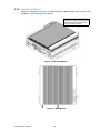
Dimension Diagram................................................................................... 3
Figure 1.1 Dimension Diagram of ITA-3630 ................................ 3
Figure 1.2 Exploded Diagram of ITA-3630 .................................. 4
Table 1.3: Part List ...................................................................... 4
1.4
1.5
Chapter
2
H/W Installation....................................5
2.1
2.2
Introduction ............................................................................................... 6
Jumpers and Connectors .......................................................................... 6
2.2.1 Jumper Description ....................................................................... 6
2.2.2 Jumper and Connector Location................................................... 7
Figure 2.1 Jumper and Connector Location on Main Board ........ 7
Table 2.1: Jumpers...................................................................... 7
Table 2.2: JLVDS1: LVDS Voltage Selection .............................. 8
Table 2.3: JCOMS1: CMOS Clear Function................................ 8
Table 2.4: PSON1: Startup-up Mode Selection........................... 8
Table 2.5: VCCGPIO1: GPIO Voltage Selection ......................... 8
I/O Connectors .......................................................................................... 9
Figure 2.2 ITA-3630-S0A1E Rear I/O Interfaces ......................... 9
Figure 2.3 ITA-3630 Front I/O Interfaces..................................... 9
2.3.1 COM Connector .......................................................................... 10
Table 2.6: COM Connector Pin Definition ................................. 10
2.3.2 HDMI Connector ......................................................................... 10
Table 2.7: HDMI Connector Pin Definition................................. 10
2.3.3 VGA Connector........................................................................... 11
Table 2.8: VGA Connector Pin Definition .................................. 11
2.3.4 USB 2.0 Connector ..................................................................... 11
Table 2.9: USB2.0 Connector Pin Definition ............................. 11
2.3.5 USB 3.0 Connector ..................................................................... 12
Table 2.10: USB3.0 Connector Pin Definition ............................. 12
2.3.6 DIO Connector ............................................................................ 12
Table 2.11: DIO Connector Pin Definition ................................... 12
2.3.7 Audio in Connector ..................................................................... 12
2.3.8 PS/2 Connector........................................................................... 13
Table 2.12: PS/2 Connector Pin Definition ................................. 13
2.3.9 LAN Connector ........................................................................... 13
Table 2.13: Ethernet Connector Pin Definition ........................... 13
Table 2.14: LED Color Definition ................................................. 13
2.3.10 Phoenix Terminal Connector ...................................................... 14
Table 2.15: Power Connector Pin Definition................................ 14
2.3.11 LPT Connector............................................................................ 14
Table 2.16: LPT Connector Pin Definition ................................... 14
2.3.12 LVDS Connector ......................................................................... 15
Table 2.17: LVDS Connector Pin Definition ................................ 15
2.3.13 LED Indicators for System Status ............................................... 15
2.3
vii
ITA-3630 User Manual
Chapter
Chapter
3
System Setup .................................... 17
3.1
Introduction ............................................................................................. 18
3.1.1 Installing Mainboard mini-PCIe card and mini SATA.................. 18
Figure 3.1 Installing Mainboard mini-PCIe card and mini SATA 18
3.1.2 Installing USB Dongle................................................................. 19
Figure 3.2 Installing USB Dongle .............................................. 19
3.1.3 Installing HDD Module ................................................................ 20
Figure 3.3 Installing HDD Module.............................................. 20
Figure 3.4 Installing HDD+CF Module....................................... 21
3.1.4 Installing Foot Stand ................................................................... 21
Figure 3.5 Installing Foot Stand................................................. 21
3.1.5 Installation Notes ........................................................................ 22
Figure 3.6 Desktop Mount ......................................................... 22
Figure 3.7 Wall Mount ............................................................... 22
4
BIOS Setting ...................................... 23
4.1
Introduction ............................................................................................. 24
Figure 4.1: Setup Program Initial Screen ................................... 24
Entering Setup ........................................................................................ 24
Figure 4.2: POST Screen ........................................................... 24
4.2.1 Main Setup.................................................................................. 25
Figure 4.3: Main Setup Screen................................................... 25
4.2.2 Advanced BIOS Features Setup................................................. 26
Figure 4.4: Advanced BIOS Features Setup Screen.................. 26
Figure 4.5 ACPI Configuration................................................... 26
Figure 4.6: CPU Configuration (1) .............................................. 27
Figure 4.7 CPU Configuration (2) .............................................. 27
Figure 4.8 SATA Configuration.................................................. 28
Figure 4.9: USB Configuration.................................................... 29
Figure 4.10:Super I/O Configuration........................................... 30
Figure 4.11Serial Port Configuration .......................................... 30
Figure 4.12:H/W Monitor COnfiguration ..................................... 31
Figure 4.13:CPU PPM Configuration.......................................... 32
Figure 4.14:APM Configuration .................................................. 33
4.2.3 Advanced Chipset Features Setup ............................................. 33
Figure 4.15Advanced Chipset Features Setup........................... 33
Figure 4.16PCH-IO Configuration .............................................. 34
Figure 4.17Chipset USB Configuration ...................................... 34
Figure 4.18PCH Azalia Configuration......................................... 35
Figure 4.19:System Agent (SA) Configuration............................ 36
Figure 4.20Graphics Configuration Menu................................... 36
Figure 4.21LCD Control.............................................................. 37
4.2.4 Boot Setup .................................................................................. 38
Figure 4.22:Boot Setup............................................................... 38
Figure 4.23Boot Option Priorities ............................................... 39
Figure 4.24:CSM Parameter....................................................... 39
4.2.5 Security Setup ............................................................................ 40
Figure 4.25:Setup Security Menu ............................................... 40
4.2.6 Save & Exit Setup....................................................................... 41
Figure 4.26:Setup Save & Exit Menu.......................................... 41
4.2
Chapter
5
Driver Installation.............................. 43
5.1
5.2
Introduction ............................................................................................. 44
Driver Installation .................................................................................... 44
5.2.1 Chipset Windows Driver Setup ................................................... 45
ITA-3630 User Manual
viii
5.2.2
5.2.3
5.2.4
5.2.5
5.2.6
Chapter
VGA Windows Driver Setup........................................................ 45
ME Windows Driver Setup .......................................................... 46
LAN Windows Driver Setup ........................................................ 46
USB 3.0 Windows Driver Setup .................................................. 47
Audio Windows Driver Installation .............................................. 47
6
GPIO Programming Guide ................49
6.1
6.2
6.3
ITA-3630 Digital DIO Definition ............................................................... 50
Configuration Sequence.......................................................................... 50
Function Call for Reference .................................................................... 54
Appendix A
Programming the Watchdog Timer..59
A.1
Programming the Watchdog Timer ......................................................... 60
A.1.1 Watchdog Timer Overview.......................................................... 60
A.1.2 Programming the Watchdog Timer ............................................. 60
Table A.1: Watchdog Timer Registers ....................................... 60
A.1.3 Example Program ....................................................................... 61
ix
ITA-3630 User Manual
ITA-3630 User Manual
x
Chapter
1
1
Overview
Sections include:
Introduction
Specifications
Power Information
Environment Specifications
Dimension Diagram
1.1 Introduction
The ITA-3630 is a fan-less, compact embedded industrial computer chassis with
CoreTM i7/i5/i3 dual core processor and wide voltage input range, which is specially
designed for intelligent transportation - Road Surveillance. This powerful computing
platform can stand operation 24 hours a day, 7 days a week.
1.2 Specifications
Processor and Chipset: CoreTM i7/i5/i3 processor + Intel® HM76 chipset
BIOS: AMI SPI 64 Mb Flash
Memory: On-board 4 GB DDR3 1333/1600 MHz
Display: Integrated graphics HD4000, with up to 256 MB SDRAM shared system memory
Dual Display:
– Single display resolution up to 2048 x 1536 @ 60 Hz
– Dual Display resolution up to 1920 x 1200 @ 60 Hz
Storage: Supports 2 x 2.5” HDD slot or 1 x CF slot and 1 x 2.5” HDD slot
Expansion Slot: Supports 1 x Mini PCIe slot
Ethernet: 2 x 10/100/1000M Ethernet (Controller chip: Intel i210-AT)
USB: 4 x USB2.0 and 2 x USB 3.0
VGA: 1 x VGA
HDMI:1 x HDMI
LVDS: 1 x LVDS (Reserved pin header on main board)
Serial I/O: 2 x DB9, RS232/422/485 with automatic flow control
Digital I/O: 1 x 8-ch GPIO
Audio: 1 x Speaker out with 2 x 4 w amplifer; 1 Mic input
Reserved Zone:
– 1 x LPT
– 1 x LVDS
– 2 x VGA (Optional PCA-5650 graphic card expansion for 2 VGA)
Dimensions (W x H x D):
– 213 x 82.7 x 240 mm (without ears)
– 253 x 86.6 x 240 mm (with ears)
Weight: 3.75 kg
1.3 Power Information
ITA-3630 supports DC 9 ~ 36 V wide voltage input
Table 1.1: Power
DC voltage input
9 V - 36 V
DC current
7.2 A - 1.8 A
DC power interface
2-pin terminal block
ITA-3630 User Manual
2
Table 1.2: Environmental Specifications
With industrial HDD: 0 ~ 40°C
With CF card: -25 ~ 60 °C (With 0.7 m/s airflow)
SAfety Certificate
Temperature
-10 ~ 50°C (With industrial standard SSD/CF/mSATA)
Storage Temperature
-40 ~ 85°C
Humidity
95% @ 40º C, non-condensing
With Compact Flash: 2 Grms @ 5 ~ 500 Hz, random, 1 hr/axis
Vibration
With 2.5” HDD: 1 Grms @ 5 ~ 500 Hz, random, 1 hr/axis
IEC60068-2-6 Sine 2G @ 5 ~ 500Hz, 1hr/axis
Shock
With Compact Flash: 20G, IEC-68-2-27, half-sine wave, 11 ms
duration
With 2.5” HDD: 10G, IEC-68-2-27, half-sine wave, 11 ms duration
Safety
UL, CCC, BSMI, CE and FCC compliant
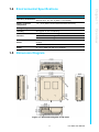
1.5 Dimension Diagram
Figure 1.1 Dimension Diagram of ITA-3630
3
ITA-3630 User Manual
Overview
Operating Temperature
Chapter 1
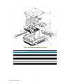
1.4 Environmental Specifications
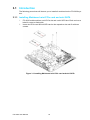
Figure 1.2 Exploded Diagram of ITA-3630
Table 1.3: Part List
1
Heat sink
9
USB tray
2
Chassis foot stand
10
HDD Tray
3
Chassis
11
2.5” HDD fix bracket
4
Front panel
12
HDD buffer rubber
5
Blank bracket
13
Thermal pad
6
Blank bracket (CF)
14
Top cover
7
USB bracket
15
Rubber foot pad
8
Main board
ITA-3630 User Manual
4
Chapter
2
2
H/W Installation
Sections include:
Introduction
Jumpers and Connectors
I/O Connectors
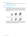
2.1 Introduction
The following sections show the internal jumpers setting and the external connectors
pin assignment for application integration.
2.2 Jumpers and Connectors
2.2.1 Jumper Description
You may configure the ITA-3630 to match the needs of your application by setting
jumpers. A jumper is a metal bridge used to close an electric circuit. It consists of two
metal pins and a small metal clip (often protected by a plastic cover) that slides over
the pins to connect them. To close a jumper, you remove the clip. Sometime a jumper
will have three pins, labelled 1, 2 and 3. In this case you would connect either pins 1
and 2, or 2 and 3.
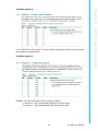
Open
Closed
2-3 Closed
The jumpers setting are schematically depicted in this manual as follows.
Open
断开
Closed
闭合
2-3 Closed
闭合 2-3
A pair of needle-nose pliers may be helpful when working with jumpers. If you have
any doubts about the best hardware configuration for your application, contact your
local distributor or sales representative before you make any changes. Generally, you
simply need a standard cable to make most connections.
ITA-3630 User Manual
6
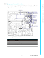
The board has a number of connectors and jumpers that allow you to configure your
system to suit your application. The table below lists the function of each of the connectors and jumpers.The locations of jumpers and connector on the board are shown
in Figure 2.1.
Chapter 2
2.2.2 Jumper and Connector Location
H/W Installation
Figure 2.1 Jumper and Connector Location on Main Board
Table 2.1: Jumpers
Label
Function
JLVDS1
LVDS voltage selection
JCOMS1
Clear CMOS settings
PSON1
Start-up mode selection
VCCGPIO1
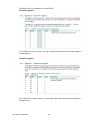
GPIO voltage selection
7
ITA-3630 User Manual
Table 2.2: JLVDS1: LVDS Voltage Selection
Closed Pins
Setting
3-4
+V12
2-4
+V5
4-6
Normal (+V3.3)*
*Default setting
+V5
+V3.3
Table 2.3: JCOMS1: CMOS Clear Function
Closed Pins
Setting
1-2
Default*
2-3
Clear CMOS
* Default setting
Table 2.4: PSON1: Startup-up Mode Selection
Closed Pins
Setting
1-2
AT Mode
2-3
ATX Mode*
* Default setting
Table 2.5: VCCGPIO1: GPIO Voltage Selection
Closed Pins
Setting
1-3
+V5_SB
2-4
Normal (+V3_SB)*
3-5
+V5
4-6
+V3.3
* Default setting
ITA-3630 User Manual
8
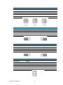
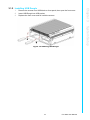
PS/2 Audio
COM x 2
USB2.0 x 4
HDMI
VGA Power Button
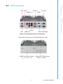
Figure 2.2 ITA-3630-S0A1E Rear I/O Interfaces
Reserved I/O connector for LPT/LVDS/COM via a cable
2 x USB2.0 connector bracket
Easy-plug CF/DOM module
Figure 2.3 ITA-3630 Front I/O Interfaces
9
ITA-3630 User Manual
H/W Installation
DIO
LAN x 2
USB3.0 x 2
DC Input
Chapter 2
2.3 I/O Connectors
2.3.1 COM Connector
ITA-3630 provides two D-sub 9-pin connectors for RS-232/422/485. The default setting is RS-232.
Table 2.6: COM Connector Pin Definition
RS-232
RS-422
RS-485
Pin
Signal Name
Signal Name
Signal Name
1
DCD
Tx-
DATA-
2
RxD
Tx+
DATA+
3
TxD
Rx+
NC
4
DTR
Rx-
NC
5
GND
GND
GND
6
DSR
NC
NC
7
RTS
NC
NC
8
CTS
NC
NC
9
RI
NC
NC
2.3.2 HDMI Connector
Table 2.7: HDMI Connector Pin Definition
Pin
Signal Name
Signal Name Signal Name
1
TMDS Data2+
11
TMDS Clock Shiled
2
TMDS Data2 Shiled
12
TMDS Clock-
3
TMDS Data2-
13
CEC
4
TMDS Data1+
14
Reserved
5
TMDS Data1 Shiled
15
SCL
6
TMDS Data1-
16
SDA
7
TMDS Data0+
17
DDC/CEC Ground
8
TMDS Data0 Shiled
18
+5V Power
9
TMDS Data0-
19
Hot Plug Detect
10
TMDS Clock+
ITA-3630 User Manual
10
ITA-3630 offers one D-sub 15-pin female connector, which supports max. resolution
of 2048 x 1563.
Pin
Signal Name
Pin
Signal Name
1
Red
9
+5V
2
Green
10
GND
3
Blue
11
NC
4
NC
12
DDC-DATA
5
GND
13
H-SYNC
6
GND
14
V-SYNC
7
GND
15
DDC-CLK
8
GND
?
?
2.3.4 USB 2.0 Connector
ITA-3630 provides four USB interface connectors, which are USB UHCI, Rev. 2.0
compliant. The USB interface can be disabled in the system BIOS setup.
Table 2.9: USB2.0 Connector Pin Definition
Pin
Signal Name
Pin
Signal Name
1
+V5(VCC)
3
USB DATA+
2
USB DATA-
4
GND
11
ITA-3630 User Manual
H/W Installation
Table 2.8: VGA Connector Pin Definition
Chapter 2
2.3.3 VGA Connector
2.3.5 USB 3.0 Connector
ITA-3630 provides two USB interface connectors, which are USB UHCI, Rev. 3.0
compliant. The USB interface can be disabled in the system BIOS setup.
Table 2.10: USB3.0 Connector Pin Definition
Pin
Signal Name
Pin
Signal Name
1
+V5(VCC)
6
StdA_SSRX+
2
D-
7
GND_DRAIN
3
D+
8
StdA_SSTX-
4
GND
9
StdA_SSTX+
5
StdA_SSRX-
2.3.6 DIO Connector
ITA-3630 provides one 8-bit DIO, D-sub 9-pin male connector without isolation
protection.
Table 2.11: DIO Connector Pin Definition
Pin
Signal Name
Pin
Signal Name
1
GPIO0
6
GPIO4
2
GPIO1
7
GPIO5
3
GPIO2
8
GPIO6
4
GPIO3
9
GPIO7
5
GND
?
?
2.3.7 Audio in Connector
ITA-3630 provides one integrated Mic-in/speaker out audio connector.
ITA-3630 User Manual
12
Chapter 2
2.3.8 PS/2 Connector
ITA-3630 provides a PS/2 keyboard and mouse connector.
Pin
Signal Name
Pin
Signal Name
1
KB_Z_DAT
4
+V5_PS2
2
MS_Z_DAT
5
KB_Z_CLK
3
GND
6
MS_Z_CLK
2.3.9 LAN Connector
ITA-3630 provides two RJ-45 Ethernet connectors with LEDs indicating network
status.
Table 2.13: Ethernet Connector Pin Definition
Pin
Signal Name
Signal Name
A1/B1
MDIO0+
MDIO0+
A2/B2
MDIO0-
MDIO0-
A3/B3
MDIO1+
MDIO1+
A4/B4
MDIO2+
MDIO2+
A5/B5
MDIO2-
MDIO2-
A6/B6
MDIO1-
MDIO1-
A7/B7
MDIO3+
MDIO3+
A8/B8
MDIO3-
MDIO3-
A9/B9
LED GREEN-
LED GREEN-
A10/B10
LED GREEN+
LED GREEN+
A11/B11
1000M LED
1000M LED
A12/B12
100m/10M LED
100m/10M LED
Table 2.14: LED Color Definition
GB Connection
Green (Upper left LED)
MB Connection
Orange (Upper left LED)
Connection Status
Green, flickering (Upper right LED)
13
ITA-3630 User Manual
H/W Installation
Table 2.12: PS/2 Connector Pin Definition
2.3.10 Phoenix Terminal Connector
ITA-3630 provides one 2-pin phoenix terminal connector for 9 V ~ 36 V power input.
Table 2.15: Power Connector Pin Definition
Pin
Signal Name
Pin
Signal Name
1
Positive pole
2
GND
2.3.11 LPT Connector
ITA-3630 provides one parallel connector (optional), which can be connected to the
reserved position on front panel via a cable.
Table 2.16: LPT Connector Pin Definition
Pin
Signal Name
Pin
Signal Name
1
LPT_z_STB#
14
LPT_AFD#
2
LPT_z_PD0
15
LPT_ERR#
3
LPT_PD1
16
LPT_INIT#
4
LPT_PD2
17
LPT_SLIN#
5
LPT_PD3
18
GND
6
LPT_PD4
19
GND
7
LPT_PD5
20
GND
8
LPT_PD6
21
GND
9
LPT_PD7
22
GND
10
LPT_ACK#
23
GND
11
LPT_BUSY
24
GND
12
LPT_PE
25
GND
13
LPT_SLCT
ITA-3630 User Manual
14
ITA-3630 provides one LPT connector (optional), which can be connected to the
reserved position on front panel via a cable.
Pin
Signal Name
Pin
Signal Name
1
TXL0+
2
TXL1+
3
TXL2+
4
TXL3+
5
TXU0+
6
TXU1+
7
TXU2+
8
TXU3+
9
TXU3-
10
TXLCLK-
11
TXL0-
12
TXL1-
13
TXL2-
14
TXL3-
15
TXU0-
16
TXU1-
17
TXU2-
18
TXUCLK+
19
TXLCLK+
20
LVCC
21
BLENABLE
22
GND
23
GND
24
GND
25
GND
26
GND
2.3.13 LED Indicators for System Status
LEDs on the rear panel are used to indicate system health and avtive status.
For detailed information of LED definition, please refer to below table.
Item
LED
1
PWR
2
HDD
Status
Color
Description
On
Green
System power is on and system is safe.
On
Yellow
There is data receiving and transmitting on SATA.
Off
There is no data receiving and transmitting on SATA.
15
ITA-3630 User Manual
H/W Installation
Table 2.17: LVDS Connector Pin Definition
Chapter 2
2.3.12 LVDS Connector
ITA-3630 User Manual
16
Chapter
3
3
System Setup
Sections include:
Installing Mainboard mini-PCIe
card and mini SATA
Installing USB Dongle
Installing HDD Module
Installing Foot Stand
Installing Notes
3.1 Introduction
The following procedures will instruct you to install all modules into the ITA-3630 system.
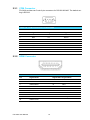
3.1.1 Installing Mainboard mini-PCIe card and mini SATA
1.
2.
ITA-3630 mainboard has a mini-PCIe slot and a mini SATA slot. Each one has a
label for users to distinguish.
Insert mini-PCIe card and mSATA card to the respective slot and fix with two
screws.
Figure 3.1 Installing Mainboard mini-PCIe card and mini SATA
ITA-3630 User Manual
18
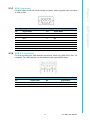
1.
2.
3.
Remove the screws near USB blade on front panel, then open the front cover.
Insert USB Dongle into USB socket.
Replave the front cover and fix it with the screws.
Chapter 3
3.1.2 Installing USB Dongle
System Setup
Figure 3.2 Installing USB Dongle
19
ITA-3630 User Manual
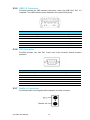
3.1.3 Installing HDD Module
The ITA-3630 reserves a space for dual HDD module and HDD+CF module. Please
refer to the following instructions to install the hard disk drive.
1. Place the HDD into 2.5” HDD holder and fill in 4 rubbers.
2. Place two HDDs onto HDD holder, and secure them with 8 screws, then sitck
the cooling pad.
3. Place HDD holder onto HDD bracket and secure it with 4 screws.
4. Connect the complete HDD module to the chassis and fix it with screws.
Figure 3.3 Installing HDD Module
ITA-3630 User Manual
20
Place rubbers into HDD holder.
Fix HDD onto the holder with 4 screws and sitck the cooling pad.
Place HDD holder onto HDD bracket and secure it with screws.
Place HDD bracket onto the chassis.
Fix CF module board onto CF tray.
Insert the CF card into CF module board and fix it with fixed plastic shell.
Place CF tray onto HDD bracket and secure it with the screws.
Chapter 3
1.
2.
3.
4.
5.
6.
7.
System Setup
Figure 3.4 Installing HDD+CF Module
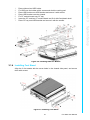
3.1.4 Installing Foot Stand
Align the 2 foot stands with the screw holes in the chassis side panel, and secure
them with screws.
Figure 3.5 Installing Foot Stand
21
ITA-3630 User Manual
3.1.5 Installation Notes
When the computer is running, no object should be placed within 30 mm above the
heatsink to avoid the impact on airflow.
To ensure an effective cooling during
operation, no object should be placed
within 30 mm above the heatsink to
avoid the impact on airflow.
Figure 3.6 Desktop Mount
Figure 3.7 Wall Mount
ITA-3630 User Manual
22
Chapter
4
BIOS Setting
4
4.1 Introduction
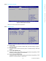
AMIBIOS has been integrated into many motherboards for over a decade. This
chapter introduces how to configure BIOS for ITA-3630 series.With the AMIBIOS
Setup program, you can modify BIOS settings and control the special features of
your computer. The Setup program uses a number of menus forsaking changes and
turning the special features on or off. This chapter describes the basic navigation of
the ITA-3630 setup screens.
Figure 4.1: Setup Program Initial Screen
AMI’s BIOS ROM has a built-in Setup program that allows users to modify the basic
system configuration. This type of information is stored in BIOS ROM so it retains the
Setup information when the power is turned off.
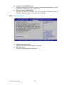
4.2 Entering Setup
Turn on the computer to enter POST screen, and BIOS and CPU information will be
shown.press <DEL> and you will immediately be allowed to enter Setup.
Figure 4.2: POST Screen
ITA-3630 User Manual
24
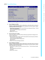
When you first enter the BIOS Setup Utility, you will enter the Main setup screen. You
can always return to the Main setup screen by selecting the Main tab. There are two
Main Setup options. They are described in this section. The Main BIOS Setup screen
is shown below.
Chapter 4
4.2.1 Main Setup
BIOS Setting
Figure 4.3: Main Setup Screen
The Main BIOS setup screen has two main frames. The left frame displays all the
options that can be configured. Grayed-out options cannot be configured; options in
blue can. The right frame displays the key legend.
Above the key legend is an area reserved for a text message. When an option is
selected in the left frame, it is highlighted in white. Often a text message will accompany it.
System Time / System Date
Use this option to change the system time and date. Highlight System Time or
System Date using the <Arrow> keys. Enter new values through the keyboard.
Press the <Tab> key or the <Arrow> keys to move between fields. The date
must be entered in MM/DD/YY format. The time must be entered in HH:MM:SS
format.
25
ITA-3630 User Manual
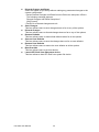
4.2.2 Advanced BIOS Features Setup
Select the Advanced tab from the ITA-3630 setup screen to enter the Advanced
BIOS Setup screen. You can select any of the items in the left frame of the screen,
such as CPU Configuration, to go to the sub menu for that item. You can display an
Advanced BIOS Setup option by highlighting it using the <Arrow> keys. All Advanced
BIOS Setup options are described in this section. The Advanced BIOS Setup screen
is shown below. The sub menus are described on the following pages.
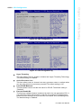
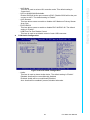
Figure 4.4: Advanced BIOS Features Setup Screen
4.2.2.1 ACPI Configuration
Figure 4.5 ACPI Configuration
Enable Hibernation
This item allows users to enable or disable Hibernation.
ACPI Sleep State
This item allows users to select APCI state during system hibernation.
S3 Video Repost
This item is used to decide whether to call VBIOS when the system resumes
from S3/SRT. The default setting is “Disabled”.
ITA-3630 User Manual
26
Chapter 4
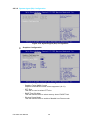
4.2.2.2 CPU Configuration
BIOS Setting
Figure 4.6: CPU Configuration (1)
Figure 4.7 CPU Configuration (2)
Hyper Threading
This item allows users to enable or disable Intel Hyper Threading Technology.
The default setting is “Enabled”.
Active Processor Core
This item allows users to choose how many processor cores to activate when
you are using a dual or quad cores processor.The default setting is “All”.
Limit CPUID Maximum
This item allows users to set the limit value for CPUID. The default setting is
“Disabled”.
Execute Disable Bit
This item is a hardware feature introduced by Intel in its new generation CPU. It
can help CPU realize self-protection under the circumstance of hostile attack
based on buffer overflow, so as to avoid the virus attack, such as blasting wave.
The default setting is “Enabled”.
27
ITA-3630 User Manual
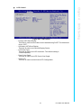
Hardware Prefectcher
This item allows users to enable or disable Hardware Prefecther Technology.
The default setting is “Enabled”.
Adjacent Cache Line Prefetch
This item allows users to enable or disable sequential access to memory. The
default setting is “Enabled”.
Intel Virtualization Technology
This item is a system virtualization technology adopted in CPU produced by
Intel. It allows multiple operating systems to run simultaneously on the same
system. It adopts Vanderpool Technology, which allows multiple systems to run
on the same system and applications can run in their own individual space. The
default setting is “Enabled”.
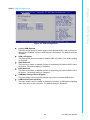
4.2.2.3 SATA Configuration
Figure 4.8 SATA Configuration
SATA Mode Selection
This item allows users to select configuration mode of SATA Controller(s). The
default setting is “AHCI”.
ITA-3630 User Manual
28
Chapter 4
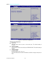
4.2.2.4 USB Configuration
BIOS Setting
Figure 4.9: USB Configuration
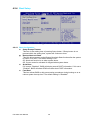
Legacy USB Support
This item allows users to enable support for traditional USB. It will be automatically set as “Disabled” when no USB device is connected. The default setting is
“Enabled”.
USB 3.0 Support
This item allows users to enable or disable USB 3.0 (XHCI). The default setting
is “Enabled”.
XHCI Hand-off
This item is to enable or disable function of supporting OS without XHCI Handoff feature. The default setting is “Enabled”.
EHCI Hand-off
This item is to enable or disable function of supporting OS without EHCI Handoff feature. The default setting is “Disabled”.
USB Mass Storage Driver Support
This item allows users to set the specific type of the connected USB device.
USB Device Power-up Delay
This item allows users to enable or disable the function of USB device reporting
max. delay time to host controller. The default setting is “Disabled”.
29
ITA-3630 User Manual
4.2.2.5 Super I/O Configuration
Figure 4.10: Super I/O Configuration
Figure 4.11 Serial Port Configuration
Serial Port 0 Configuration
Serial Port
This item allows users to open or close serial port. The default setting is
“Enabled”.
Serial Port Mode
This item allows users to set serial port as RS232/422/485. The default setting is
“RS232”.
Change Settings
IO=3F8h; IRQ=4;
IO=3F8h; IRQ=3,4,5,6,7,10,11,12;
This item allows users to select IO address and IRQ to change serial port settings.
ITA-3630 User Manual
30
Device Mode
This item allow users to select device mode. The default setting is “Normal
Mode”.
4.2.2.6 H/W Monitor
Chapter 4
BIOS Setting
Figure 4.12: H/W Monitor COnfiguration
PC Health Status
This item is used to hardware safety detection. BIOS will display the current system temperature, CPU temperature and other related voltage values. All these
parameters have a certain range, so operations out of the range should be
avoided.
31
ITA-3630 User Manual
4.2.2.7 CPU PPM Configuration
Figure 4.13: CPU PPM Configuration
EIST
This item is used to set CPU SpeedStep function. The default setting is
“Enabled”.
Turbo Mode
This item is used to set CPU Turbo mode function. The default setting is
“Enabled”.
CPU C3/C6/7 Report
This item is used to set CPU C-state function. The default setting is “Enabled”.
Config TDP LOCK
This item is used to set Config TDP LOCK function. The default setting is “Disabled”.
ACPI T State
This item is used to set ACPI T State function. The default setting is “Disabled”.
ITA-3630 User Manual
32
Chapter 4
4.2.2.8 APM Configuration
BIOS Setting
Figure 4.14: APM Configuration
Board Power Mode
This item is used to set power on mode: AT or ATX mode.
4.2.3 Advanced Chipset Features Setup
Figure 4.15 Advanced Chipset Features Setup
33
ITA-3630 User Manual
4.2.3.1 PCH-IO Configuration
Figure 4.16 PCH-IO Configuration
SLP_S4 Assertion Width
This item is used to set the min. delay of SLP_S4# signal when booting. The
default setting is “4-5 Seconds”.
Restore AC Power Loss
This item is used to set power status when the power in on.
Power Off: Power button should be pressed after the power is on.
Power On: No action required after the power is on.
Last State: Resume to the last state before the power is off.
USB Configuration
Figure 4.17 Chipset USB Configuration
– XHCI Pre-Boot Driver
This item allows users to enable or disable XHCI Pre-Boot Driver. The default
setting is “Enable”.
ITA-3630 User Manual
34
– Azalia
This item is used to detect Azalia device. The default setting is “Enable”.
Disabled: Azalia will be unconditionally disabled.
Enabled: Azalia will be unconditionally Enabled.
Auto: Azalia will be enabled if present, disabled otherwise.
35
ITA-3630 User Manual
BIOS Setting
Figure 4.18 PCH Azalia Configuration
Chapter 4
– xHCI Mode
This item is used to select xHCI controller mode. THe default setting is
“Smart Auto”.
– HS Port #1/#2/#3/#4 Switchable
Enable: BIOS will let the port connect to EHCI; Disable: BIOS will let the port
connect to xHCI. The default setting is “Enable”.
– xHCI Streams
This item allows users to enable or disable xHCI Maximum Primary Stream
Array Size.
– EHCI1/EHCI2
This item allows users to enable or disable EHCI #1/EHCI #2. The default
setting is “Enable”.
– USB Ports Per-Port Disable Control
This item is used to set disable control of each USB connector.
PCH Azalia Configuration
4.2.3.2 System Agent (SA) Configuration
Figure 4.19: System Agent (SA) Configuration
Graphics Configuration
–
–
–
–
Figure 4.20 Graphics Configuration Menu
Graphics Turbo IMON Current
Graphics turbo IMON current values supported (14-31).
GTT Size
This item is used to select GTT size.
DVMT Total Gfx Mem
This item allows users to select memory size of DVMT Total.
Gfx Low Power Mode
This item allows users to enable of disable Low Power mode.
ITA-3630 User Manual
36
LCD Control
–
–
–
–
Figure 4.21 LCD Control
Primary IGFX Boot Display
This item is used to select video device started during POST. The default setting is “CRT”.
Secondary IGFX Boot Display
This item is used to set Second Display Device.
LCD Panel Type
This item is used to set LCD resolution. The default setting is
“1024x768(24bit)”.
Panel Color Depth
This item is used to set LFP Panel Color Depth.
Active LFP
This item is used to select Active LFP Configuration.
37
ITA-3630 User Manual
BIOS Setting
–
Chapter 4
4.2.4 Boot Setup
Figure 4.22: Boot Setup
4.2.4.1 Boot Configuration
Setup Prompt Timeout
This item is the waiting time of pressing Setup button. If Setup button is not
pressed within the setting time, system will continue to boot.
Bootup NumLock State
This item allows users to active Bootup NumLock State function after the system
is power on to DOS. The default setting is “On”.
On: NumLock function is on when system boots.
Off: Cursor control is activated for keypad when system boots.
Quiet Boot
If it is set to “Disabled”, BIOS will display normal POST information; If it is set to
“Enabled”, BIOS will show OEM icon rather than POST information.
Fast Boot
This item allows BIOS to skip some testing procedures during booting so as to
reduce system boot-up time. The default setting is “Disabled”.
ITA-3630 User Manual
38
Chapter 4
4.2.4.2 Boot Option Priorities
BIOS Setting
Figure 4.23 Boot Option Priorities
This item is used to set device boot sequence.
4.2.4.3 CSM Parameter
Figure 4.24: CSM Parameter
Launch CSM
This item allows user to enable or disable CSM. The default setting is “Enable”.
Boot option filter
This item is used to control boot device system. The default setting is “UEFI and
Legacy”.
Launch PXE OpROM policy
This item is used to control UEFI execution and backward compatibility of PXE
OpROM. The default setting is “Do not Launch”.
Launch Storage OpROM policy
This item is used to control UEFI execution and backward compatibility of PXE
OpROM. The default setting is ““Legacy only”.
39
ITA-3630 User Manual
Launch Video OpROM policy
This item is used to control UEFI execution and backward compatibility of PXE
OpROM. The default setting is ““Legacy only”.
Other PCI device ROM priority
This item is used for PCI device that is not the same as network, which is
defined by massive storage or video booted by OpROM.
4.2.5 Security Setup
Figure 4.25: Setup Security Menu
Administrator Password
This item is used to set Administrator Password.
User Password
This item is used to set User Password.
ITA-3630 User Manual
40
Chapter 4
4.2.6 Save & Exit Setup
BIOS Setting
Figure 4.26: Setup Save & Exit Menu
Save Changes and Exit
When you have completed system configuration, select this option to save your
changes, exit BIOS setup and reboot the computer so the new system configuration parameters can take effect.
1.Select Save Changes and Exit from the Exit menu and press <Enter>. The following message appears:
Save Configuration Changes and Exit Now?
[Ok] [Cancel]
2.Select Ok or Cancel.
Discard Changes and Exit
Select this option to quit Setup without making any permanent changes to the
system configuration.
1.Select Exit Discard Changes and Exit from the Exit menu and press <Enter>.
The following message appears:
Discard Changes and Exit Setup Now?
[Ok] [Cancel]
2.Select Ok to discard changes and exit.
Save Changes and Reset
When you have completed system configuration, select this option to save your
changes, exit BIOS setup and reboot the computer so the new system configuration parameters can take effect.
1.Select Save Changes and Reset and press <Enter>. The following message
appears:
Save configuration and Reset?
[Yes] [No]
2.Select Ok or Cancel.
41
ITA-3630 User Manual
Discard Changes and Reset
Select this option to quit Setup without making any permanent changes to the
system configuration.
1.Select Discard Changes and Reset from the Exit menu and press <Enter>.
The following message appears:
Discard Changes and Reset Setup Now?
[Ok] [Cancel]
2.Select Ok to discard changes and exit.
Save Changes
This item allows users to save changes done so far to any of the options.
Discard Changes
This item allows users to discard changes done so far to any of the options.
Restore Defaults
This item allows users to restore/load default values for all the options.
Save as User Defaults
This item allows users to save the changes done so far as user defaults.
Restore User Defaults
This item allows users to restore the user defaults to all the options.
Boot Override
This item allows users to set boot device.
Launch EFI Shell from filesystem device
This item allows to boot EFI shell from system file device.
ITA-3630 User Manual
42
Chapter
5
5
Driver Installation
Sections include:
Chipset Windows Driver Setup
VGA Windows Driver Setup
ME Windows Driver Setup
LAN Windows Driver Setup
USB 3.0 Windows Driver Setup
Audio Windows Driver Setup
5.1 Introduction
Advantech offers a complete range of Device Driver and software supports for Windows programming developers. You can apply the Windows Device Drivers to the
most popular Windows Programming tools, such as Visual C++, Visual Basic, Borland C++ Builder and Borland Delphi.
Here Windows 7 is taken as an example.
5.2 Driver Installation
Insert the driver CD into your system’s CD-ROM drive. You can see the ITA-3630
driver folder items.
ITA-3630 User Manual
44
Insert the driver CD into your system’s CD-ROM drive. You can see the driver folder
items. Navigate to the "Drv_01Chipset" folder and click "Setup" to complete the
installation of the driver.
Chapter 5
5.2.1 Chipset Windows Driver Setup
Driver Installation
5.2.2 VGA Windows Driver Setup
Insert the driver CD into your system’s CD-ROM drive. You can see the driver folders
items. Navigate to the "Drv_02VGA" folder and click "Setup" to complete the installation of the drivers.
45
ITA-3630 User Manual
5.2.3 ME Windows Driver Setup
Insert the driver CD into your system’s CD-ROM drive. You can see the driver folders
items. Navigate to the "Drv_03ME" folder and click "Setup" to complete the installation of the drivers.
5.2.4 LAN Windows Driver Setup
Insert the driver CD into your system’s CD-ROM drive. You can see the driver folders
items. Navigate to the "Drv_04LAN" folder and click "Autorun" to complete the installation of the drivers.
ITA-3630 User Manual
46
Insert the driver CD into your system’s CD-ROM drive. You can see the driver folders
items. Navigate to the "Drv_05USB3.0" folder, and click "Setup" to complete the
installation of the drivers.
Chapter 5
5.2.5 USB 3.0 Windows Driver Setup
Driver Installation
5.2.6 Audio Windows Driver Installation
Insert the driver CD into your system’s CD-ROM drive. You can see the driver folders
items. Navigate to the "Drv_ 06AUDIO”" folder and click "WDM_R264.exe" to complete the installation of the drivers.
47
ITA-3630 User Manual
ITA-3630 User Manual
48
Chapter
6
6
GPIO Programming
Guide
This chapter introduces GPIO programming Guide.
Please carefully read and study the below screenshots and source codes in blue.
Please download specification of NXP Semiconductors PCA955 for programming.
6.1 ITA-3630 Digital DIO Definition
See Section 2.3.6.
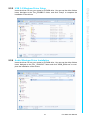
6.2 Configuration Sequence
ITA-3630’s GPIO is realized through PCA9554 GPIO IC connected to ICH SMBUS.
Therefore, the configuration and access to GPIO IC is completed by IO Space
accessing to ICH SMBUS controller.
Below is the diagram of ICH SMBUS IO Space:
SMB_BASE + Offset
Mnemonic
REgister Name
Default
Type
00h
HST_STS
Host Status
00h
R/WC, RO,
R/WC (special)
02h
HST_CNT
Host Control
00h
R/W, WO
03h
HST_CMD
Host Command
00h
R/W
04h
XMIT_SLVA
Transmit Slave
Address
00h
R/W
05h
HST_D0
Host Data 0
00h
R/W
06h
HST_D1
Host Data 1
00h
R/W
For ITA-3630, IO address of the above SMB_BASE is 0xF040.
The detailed SMBUS IO control access code, please refer to Chapter 3.
The corresponding SMBUS slave address of PCA9554 of GPIO 00 - GPIO 07 on
ITA-3630 is 0x40 (8bit address):
GPIO 00 – GPIO 07: PCA9554 0x40 (IO0 – IO7)
ITA-3630 User Manual
50
Chapter 6
Below is the sketch of PCA9554:
GPIO Programming Guide
Below is the diagram of PCA9554 register:
51
ITA-3630 User Manual
PCA9554 has in all 4 registers to control GPIO.
PCA9554 register 0:
If one GPIO Pin is set to Input, you can read input value from the bit that register 0
corresponds to.
PCA9554 register 1:
If one GPIO Pin is set to Output, you can read input value from the bit that register 1
corresponds to.
ITA-3630 User Manual
52
Chapter 6
PCA9554 register 2:
PCA9554 register 3:
Register 3 is used to set each GPIO as Input or Output:
If the bit is ‘0’, the corresponding GPIO pin is set as Ouput;
If the bit is ‘1’, the corresponding GPIO pin is set as Input.
53
ITA-3630 User Manual
GPIO Programming Guide
If one GPIO Pin is set to Input, you can control the polarity of input pin from the bit
that register 2 corresponds to.
Example:
Here take ITA-3630 as an example. Assume GPIO 00 is set as Output and GPIO 7 is
set as Input, with two pins interconnected, how to set the corresponding register?
GPIO 00 corresponds to PCA9554 0x40 IO0, while GPIO 07 corresponds to
PCA9554 0x40 IO7.
Set GPIO 00 as Output:
1. Read SMBUS slave 0x40 register 3 byte value;
2. Set bit 0 of the value read in step 1 as 0 and write it to SMBUS slave 0x40 register 3;
3. Read SMBUS slave 0x40 register 1 byte value;
4. Set bit 0 of the value read in step 3 as 0 or 1 according to low or high of the output value, then write it back to SMBUS slave 0x40 register 1.
Set GPIO 07 as Input:
1. Read SMBUS slave 0x40 register 3 byte value;
2. Set bit 7 of the value read in step 1 as 1 and write it to SMBUS slave 0x40 register 3;
3. Read SMBUS slave 0x40 register 0 byte value;
4. Decide low or high of the input value through bit7 value read in step3.
6.3 Function Call for Reference
ICH SMBUS Access Code
(The following code is realized by simulating the access of BIOS to SMBUS. It uses
Borand C++ 3.1 for compiling and is successfully tested under DOS (So far, it is not
tested under other OSs).
#define SMBUS_PORT 0xF040//SMB_BASE?0xF040
typedef unsigned char BYTE;
/////////////////////////////////////////////////////////////////////////////////////////////////////
BYTE smbus_read_byte(BYTE addr, BYTE offset)
// Read SMBUS Register byte value. Read one byte value each time. addr is slave
address (such as 0x40), and offset is register offset.
{
int
i;
BYTE data;
outportb(SMBUS_PORT + 4, (addr | 1));//
Write
slave
address
to
SMB_BASE + 4 (When reading, bit 0 of slave address should be set as 1, so here
addr|1 is available)
newiodelay();//delay
newiodelay();//delay
chk_smbus_ready();// Whether SMBUS is ready
outportb(SMBUS_PORT + 3, offset);// Write register offset to SMB_BASE +
3
ITA-3630 User Manual
54
outportb(SMBUS_PORT + 2, 0x48);// Write SMBUS
SMB_BASE + 2. 0x48 means starting byte data transmission
newiodelay();//delay
newiodelay();//delay
command
to
chk_smbus_ready();//Whether SMBUS is ready
return(inportb(SMBUS_PORT + 5));// Byte value read from SMB_BASE + 5
}
/////////////////////////////////////////////////////////////////////////////////////////////////////
void
smbus_write_byte(BYTE addr, BYTE offset, BYTE value)
// Write SMBUS Register byte value. Write one byte value each time. addr is slave
address (such as 0x40), and offset is register offset.
{
int
i;
outportb(SMBUS_PORT + 4, addr);// Write slave address to SMB_BASE +
4 (When writing, slave address bit 0 should be set as 0)
moredelay();//longer delay
moredelay();//longer delay
chk_smbus_ready();//Whether SMBUS is ready
outportb(SMBUS_PORT + 3, offset);// Write register offset to SMB_BASE +
3
moredelay();//longer delay
moredelay();//longer delay
outportb(SMBUS_PORT + 5, value);//Write data value to SMB_BASE + 5
moredelay();//longer delay
moredelay();//longer delay
outportb(SMBUS_PORT + 2, 0x48);// Write SMBUS
SMB_BASE + 2.. 0x48 means starting byte data transmission.
moredelay();//longer delay
moredelay();//longer delay
command
to
for (i = 0; i <= 0x100; i++)
55
ITA-3630 User Manual
GPIO Programming Guide
for (i = 0; i <= 0x100; i++)
{
newiodelay();//longer delay
}
Chapter 6
newiodelay();//delay
newiodelay();//delay
{
newiodelay();//longer delay
}
chk_smbus_ready();//?Whether SMBUS is ready
}
/////////////////////////////////////////////////////////////////////////////////////////////////////
int
chk_smbus_ready()
//To decide whether SMBUS is ready or has completed the action, you should wait for
a long time to check whether SMBUS has successfully transmitted the command.
Since error may rarely occurs, BIOS code does not make judgement on the return
value of this function in read and write of SUMBUS byte.
{
int
i, result = 1;
BYTE data;
for (i = 0; i <= 0x800; i++)
{
//SMB_BASE + 0 is SMBUS status value
data = inportb(SMBUS_PORT);//Read SMBUS status value once
data = check_data(SMBUS_PORT);//Read SMBUS status value several timesoutportb(SMBUS_PORT, data);//?Write back SMBUS status value which
will clear status value (Write 1 to the corresponding bit means clearing status)
if (data & 0x02)
{
//If bit 1 is set (which means the command is completed),
SMBUS is ready
result = 0;//SMBUS ready
break;
}
if (!(data & 0xBF))
{
//If all bits are 0 except bit 2 (which means error occurs on
SMBUS), SMBUS is ready
result = 0;//SMBUS ready
break;
}
if (data & 0x04)
{
//If bit 2 is set (which means error occurs on SMBUS), error
occurs on SMBUS which is rarely the case
result = 1;//SMBUS error
break;
}
}
ITA-3630 User Manual
56
Chapter 6
returnresult;
}
/////////////////////////////////////////////////////////////////////////////////////////////////////
BYTE check_data(WORD addr)
{
int
i;
BYTE data;
returndata;
}
/////////////////////////////////////////////////////////////////////////////////////////////////////
void
newiodelay()
//Shorter delay
{
outportb(0xeb, 0);//IO port 0xeb No real device occupies. Write a value to
this port can realize delay function. You can also choose other method according to
the real situation.
}
/////////////////////////////////////////////////////////////////////////////////////////////////////
void
moredelay()
//Longer delay
{
int
i;
for (i = 0; i < 20; i++)
{
outportb(0xeb, 0);//IO port 0xeb No real device occupies. Write a
value to this port can realize delay function. You can also choose other method
according to the real situation.
}
}
************************************************************************
GPIO Simcodes
(Here GPIO 00 and GPIO 07 in Chapter 2 are taken as examples)
Output High to GPIO 00:
data = smbus_read_byte(0x40, 0x03);// Read slave 0x40 register 3 byte
57
ITA-3630 User Manual
GPIO Programming Guide
for(i = 0; i <= 6; i++)
{
data = inportb(addr);
if (data != 0)
break;
}
data &= 0xfe;//bit 0 is set as 0
smbus_write_byte(0x40, 0x03, data)//Write back. GPIO 00 is set for output
data = smbus_read_byte(0x40, 0x01)//Read slave 0x40 register 1
data |= 0x01;//bit 0 is set as 1 which stands for high
smbus_write_byte(0x40, 0x01, data)//Write back. Output high value
Read Input Value from GPIO 07:
data = smbus_read_byte(0x40, 0x03);//Read slave 0x40 register 3 byte
data |= 0x80;//bit 7??1
smbus_write_byte(0x40, 0x03, data)//Write back. GPIO 07 is set for input
data = smbus_read_byte(0x40, 0x00)//Read slave 0x40 register 0. Then,
the response value of bit 7 should know whether the input is low or high
ITA-3630 User Manual
58
Appendix
A
A
Programming the
Watchdog Timer
A.1 Programming the Watchdog Timer
The ITA-3630's watchdog timer can be used to monitor system software operation
and take corrective action if the software fails to function within the programmed
period. This section describes the operation of the watchdog timer and how to program it.
A.1.1 Watchdog Timer Overview
The watchdog timer is built into the super I/O controller SMSC SCH3114. It provides
the following user-programmable functions:
Can be enabled or disabled via user program
Timer can be set from 1 to 255 seconds or 1 to 255 minutes
Generates an interrupt or resets signal if the software fails to reset the timer
before time-out
A.1.2 Programming the Watchdog Timer
The I/O port address of the watchdog timer is 680h (hex).
Table A.1: Watchdog Timer Registers
Address: 680h (hex)
Register Shift Read/Write
Description
65 (hex)
write
Set seconds or minutes as units for the timer.
Write 0 to bit 7: set second as counting unit. [default]
Write 1 to bit 7: set minutes as counting unit.
write
0: Stop timer [default]
01~FF (hex): The amount of the count, in seconds or minutes, depends on the value set in register 65 (hex). This
number decides how long the watchdog timer waits for
strobe before generating an interrupt or reset signal. Writing
a new value to this register can reset the timer to count with
the new value.
read/write
Configure watchdog timer
Bit 1:Write 1 to enable keyboard to reset the timer, 0 to disable. [default]
Bit 2: Write 1 to enable mouse to reset the timer, 0 to disable.[default]
Bit 7~4: Set the interrupt mapping of watchdog timer:
1111=IRQ15
……
0011=IRQ3
0010=IRQ2
0001=IRQ1
0000=Disable [default]
read/write
Control watchdog timer
Bit0: Read watchdog state; 1=Timer timeout
Bit2: Write 1 to immediately generate timeout signal, and
automatically return to 0 (Write only).
Bit3: Writer 1 to allow triggering of timer timeout when P20
is effective, 0 to disable. [default]
66 (hex)
67 (hex)
68 (hex)
ITA-3630 User Manual
60
;----------------------------------------------------------1. Enable watchdog timer and set 10 sec. as timeout interval
;----------------------------------------------------------Mov dx,A65h ; Select register 65h, watchdog timer I/O port address 680h+ register
shifts 65h
Mov al,80h ; Set second as counting unit
Out dx,al
Mov dx,A66h ; Select register 66h, watchdog timer I/O port address 680h+ register
shift 66h
Mov al,10 ; Set timeout interval as 10 seconds and start counting
Out dx,al
;----------------------------------------------------------2. Enable watchdog timer and set 5 min. as timeout interval
;----------------------------------------------------------Mov dx,A65h ; Select register 65h, watchdog timer I/O port address 680h+ register
shifts 65h
Mov al,00h ; Set minute as counting unit
Out dx,al
680h
Mov dx,A66h ; Select register 66h, watchdog timer I/O port address 680h+ register
shifts 66h
Mov al,5 ;Set timeout interval as 5 minutes and start counting
Out dx,al
;----------------------------------------------------------3. Enable watchdog timer to be reset by mouse
;----------------------------------------------------------Mov dx,A67h ; Select register 67h, watchdog timer I/O port address 680h+ register
shifts 67h
In al,dx
Or al,4h ; Enable watchdog timer to be reset by mouse
Out dx,al
;----------------------------------------------------------4. Enable watchdog timer to be reset by keyboard
;----------------------------------------------------------Mov dx,A67h ; Select register 67h, watchdog timer I/O port address 680h+ register
shifts 67h
In al,dx
Or al,2h ; Enable watchdog timer to be reset by keyboard
Out dx,al
;----------------------------------------------------------5. Generate a time-out signal without timer counting
;----------------------------------------------------------Mov dx,A68h ; Select register 68h, watchdog timer I/O port address 680h+ register
shifts 68h
In al,dx
Or al,4h ; Generate a time-out signal
Out dx,al
;----------------------------------------------------------61
ITA-3630 User Manual
Appendix A Programming the Watchdog Timer
A.1.3 Example Program
www.advantech.com
Please verify specifications before quoting. This guide is intended for reference
purposes only.
All product specifications are subject to change without notice.
No part of this publication may be reproduced in any form or by any means,
electronic, photocopying, recording or otherwise, without prior written permission of the publisher.
All brand and product names are trademarks or registered trademarks of their
respective companies.
© Advantech Co., Ltd. 2014