1
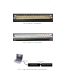
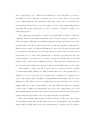
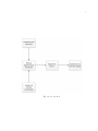
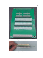
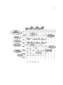
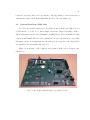
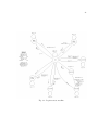
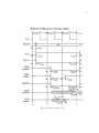
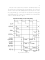
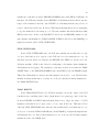
RE-ENGINEERING OF A BLACK BOX FOR THE PURPOSE OF UPGRADE
AND MAINTENANCE
by
Nathanael R. Weidler
A report submitted in partial fulfillment
of the requirements for the degree
of
MASTER OF SCIENCE
in
Computer Engineering
Approved:
Dr. Tam Chantem
Major Professor
Dr. Jacob Gunther
Committee Member
Dr. Koushik Chakraborty
Committee Member
UTAH STATE UNIVERSITY
Logan, Utah
2014
ii
Copyright
c Nathanael R. Weidler 2014
All Rights Reserved
iii
Abstract
Re-Engineering of a Black Box for the Purpose of Upgrade and Maintenance
by
Nathanael R. Weidler, Master of Science
Utah State University, 2014
Major Professor: Dr. Tam Chantem
Department: Electrical and Computer Engineering
There existed an aging electrical system that needed to be upgraded. An upgrade was
necessary for this system because the cost to maintain the aging technology was becoming
too great. There were, however, no available schematics or technical papers describing this
system. In order to upgrade the system, it first needed to be reverse engineered. The
system to be upgraded was a device that would pass data back and forth from a personal
computer to a proprietary storage device. The device to be upgraded communicated with
the personal computer over a standard Small Computer System Interface (SCSI) interface
and with the proprietary storage device through a non-standard 92-pin interface. The SCSI
interface needed to be replaced by an Ethernet interface. The 92-pin interfaced needed
to be reverse engineered so that it could continue to interface with the storage device as
that was not going to be changed in any way. This report describes this process from the
beginning to the end. It includes the different phases needed to reverse engineer the custom
interface and the design and testing of the newly designed electrical system to replace the
aging technology.
(51 pages)
iv
Public Abstract
Re-Engineering of a Black Box for the Purpose of Upgrade and Maintenance
by
Nathanael R. Weidler, Master of Science
Utah State University, 2014
Major Professor: Dr. Tam Chantem
Department: Electrical and Computer Engineering
An entity had a product, and became concerned that their technology was aging and
becoming very expensive to build. That entity decided that this product needed to be
upgraded to deal with these concerns. In order to upgrade the product, it needed to be
reverse engineered first. This is because no plans or schematics existed for the current product. The re-engineered product needed to continue to communicate with existing hardware.
This paper contains the process of reverse engineering and re-engineering the product for
the entity.
v
I would like to dedicate this work to my wife Jenni and son Benjamin. This is for them.
vi
Acknowledgments
I would like to acknowledge the team of highly skilled and qualified engineers who
helped me through every step of this process. They are Jason Swasey, Melvin Graff, and
Brent Ware. This project would not have been a success without their contributions.
I would also like to thank Wally Gibbons as he was my mentor while I designed the
schematics for the replacement board.
Finally, I would like to thank Dr. Tam Chantem for aiding and advising me on this
project.
Nathanael R. Weidler
vii
Contents
Page
Abstract . . . . . . . . . . . . . . . . . . . . . . . . . . . . . . . . . . . . . . . . . . . . . . . . . . . . . . .
iii
Public Abstract . . . . . . . . . . . . . . . . . . . . . . . . . . . . . . . . . . . . . . . . . . . . . . . . .
iv
Acknowledgments . . . . . . . . . . . . . . . . . . . . . . . . . . . . . . . . . . . . . . . . . . . . . . .
vi
List of Figures . . . . . . . . . . . . . . . . . . . . . . . . . . . . . . . . . . . . . . . . . . . . . . . . . .
ix
Acronyms . . . . . . . . . . . . . . . . . . . . . . . . . . . . . . . . . . . . . . . . . . . . . . . . . . . . . .
x
1 Introduction . . . . . . . . . . . . . . . . . . . . . . . . . . . . . . . . . . . . . . . . . . . . . . . . .
1.1 Background . . . . . . . . . . . . . . . . . . . . . . . . . . . . . . . . . . . .
1.2 Goals . . . . . . . . . . . . . . . . . . . . . . . . . . . . . . . . . . . . . . .
1
1
4
2 Analysis of Current Functionality . . . . . . . . . . . . . . . . . . . . . . . . . . . . . . . .
6
3 Limited Manual Dissection of the Pass-Through Box . . . . . . . . . . . . . . . .
7
4 Reverse Engineering of the Pass-Through
4.1 Pin Characterization . . . . . . . . . . . .
4.2 Data Bus . . . . . . . . . . . . . . . . . .
4.3 Ramps . . . . . . . . . . . . . . . . . . . .
4.4 The Search for a Standard . . . . . . . . .
4.5 PCI Protocol Background . . . . . . . . .
4.5.1 Address Phase . . . . . . . . . . .
4.5.2 Claiming the Transaction . . . . .
4.5.3 Data Phase . . . . . . . . . . . . .
4.5.4 Illegal Behavior . . . . . . . . . . .
4.5.5 Mandatory PCI Signals . . . . . .
5 Designing a New Pass-Through Box . .
5.1 FPGA . . . . . . . . . . . . . . . . . .
5.2 Processor . . . . . . . . . . . . . . . .
5.3 Power . . . . . . . . . . . . . . . . . .
5.4 MICTOR Connectors . . . . . . . . .
5.5 Universal Serial Bus (USB) Chip . . .
Box
. . .
. . .
. . .
. . .
. . .
. . .
. . .
. . .
. . .
. . .
....
. . .
. . .
. . .
. . .
. . .
.
.
.
.
.
.
.
.
.
.
.
....
. . .
. . .
. . .
. . .
. . .
6 Implementation and Testing of New Design . .
6.1 Smoke Test . . . . . . . . . . . . . . . . . . . .
6.2 PCI Implementation in the FPGA . . . . . . .
6.3 Arbiter . . . . . . . . . . . . . . . . . . . . . .
6.4 PCI State Machine . . . . . . . . . . . . . . . .
....
. . .
. . .
. . .
. . .
. . .
. . .
. . .
. . .
. . .
. . .
.
.
.
.
.
.
....
. . .
. . .
. . .
. . .
. . .
. . .
. . .
. . .
. . .
. . .
....
. . .
. . .
. . .
. . .
. . .
.....
. . . .
. . . .
. . . .
. . . .
.
.
.
.
.
.
.
.
.
.
.
....
. . .
. . .
. . .
. . .
. . .
. . .
. . .
. . .
. . .
. . .
....
. . .
. . .
. . .
. . .
. . .
. . .
. . .
. . .
. . .
. . .
....
. . .
. . .
. . .
. . .
. . .
....
. . .
. . .
. . .
. . .
. . .
.
.
.
.
.
.
....
. . .
. . .
. . .
. . .
....
. . .
. . .
. . .
. . .
.
.
.
.
.
...
. .
. .
. .
. .
. .
. .
. .
. .
. .
. .
....
. . .
. . .
. . .
. . .
. . .
....
. . .
. . .
. . .
. . .
9
9
12
13
13
14
15
15
17
17
18
. . 19
.
19
.
20
.
20
.
20
.
21
...
. .
. .
. .
. .
22
22
23
29
29
viii
6.4.1
6.4.2
Target States . . . . . . . . . . . . . . . . . . . . . . . . . . . . . . .
Initiator States . . . . . . . . . . . . . . . . . . . . . . . . . . . . . .
31
35
7 Conclusion and Future Work . . . . . . . . . . . . . . . . . . . . . . . . . . . . . . . . . . . . 40
References . . . . . . . . . . . . . . . . . . . . . . . . . . . . . . . . . . . . . . . . . . . . . . . . . . . . . . 41
ix
List of Figures
Figure
Page
1.1
Male side - 92-pin interface. . . . . . . . . . . . . . . . . . . . . . . . . . . .
2
1.2
Female side - 92-pin interface. . . . . . . . . . . . . . . . . . . . . . . . . . .
2
1.3
Setup read/write data from proprietary hard drive. . . . . . . . . . . . . . .
2
1.4
Project flow. . . . . . . . . . . . . . . . . . . . . . . . . . . . . . . . . . . .
5
4.1
Breakout board front. . . . . . . . . . . . . . . . . . . . . . . . . . . . . . .
11
4.2
Breakout board top. . . . . . . . . . . . . . . . . . . . . . . . . . . . . . . .
11
4.3
Breakout board side. . . . . . . . . . . . . . . . . . . . . . . . . . . . . . . .
12
4.4
Start of a ramp fie viewed in a hex editor. . . . . . . . . . . . . . . . . . . .
14
4.5
PCI transaction. . . . . . . . . . . . . . . . . . . . . . . . . . . . . . . . . .
16
5.1
Re-designed pass-through box populated board. . . . . . . . . . . . . . . . .
21
6.1
System level block diagram. . . . . . . . . . . . . . . . . . . . . . . . . . . .
25
6.2
Registers state machine. . . . . . . . . . . . . . . . . . . . . . . . . . . . . .
26
6.3
Rabbit external read. . . . . . . . . . . . . . . . . . . . . . . . . . . . . . . .
27
6.4
Rabbit external write. . . . . . . . . . . . . . . . . . . . . . . . . . . . . . .
28
6.5
Arbiter state machine. . . . . . . . . . . . . . . . . . . . . . . . . . . . . . .
30
6.6
PCI state machine. . . . . . . . . . . . . . . . . . . . . . . . . . . . . . . . .
32
x
Acronyms
C/BE
Command/Byte Enable
COTS
Commercial off the Shelf
DEVSEL
Device Select
FPGA
Field Programable Gate Array
GNT
Grant
I/O
Input/Output
IORD
In/Out Read
IOWR
In/Out Write
IRDY
Initiator Ready
LSB
Least Significant Bit
MICTOR
Matched Impedance Connector
PC
Personal Computer
PCB
Printed Circuit Board
PCI
Peripheral Component Interconnect
RAM
Random Access Memory
SCSI
Small Computer System Interface
TRDY
Target Ready
UART
Universal Asynchronous Receiver/Transmitter
USB
Universal Serial Bus
VHDL
VHSIC Hardware Description Language
VHSIC
Very High Speed Integrated Circuit
1
Chapter 1
Introduction
1.1
Background
There was an entity with an aging technology who wanted to upgrade this technology.
This entity, hereto referred to as the customer, expressed a desire for the author to upgrade
this technology. The author accepted this interesting project, and therefore agreed to aid
the customer in their desire.
The technology that the customer wanted to upgrade will be referred to as, the passthrough box, and is the subject of this project. This box will be referred to as the passthrough box because this name describes its basic functionality. This device (the passthrough box) enables the customer to transfer data from a Personal Computer (PC) to
another proprietary device which is equivalent to an external hard drive. This proprietary
hard drive will not be discussed here as it is outside the scope of this report. The passthrough box is the interface for the customer to transfer data from a PC to their proprietary
external hard drive. The current methodology for transferring data from a PC through the
pass-through box to the proprietary hard drive takes two steps. In step 1, the PC connects
to the pass-through box using an external Small Computer System Interface (SCSI) cable.
In step 2, the pass-through box connects to the proprietary hard drive through a 92-pin
interface. The male side of the 92-pin interface can be see in Fig. 1.1 and the female side
can be seen in Fig. 1.2. The data is transferred directly to the proprietary hard drive from
the PC through the pass-through box. It was not believed that the pass through box stores
the data, but simply transfers it in real time. An illustration of this can be seen in Fig. 1.3.
The task at hand was not only to upgrade the pass-through box, but was also to
reverse-engineer it. The customer had little working knowledge of how the pass-through
box transferred data. For this reason, this project was not just an upgrade, but a reverse
2
Fig. 1.1: Male side - 92-pin interface.
Fig. 1.2: Female side - 92-pin interface.
Fig. 1.3: Setup read/write data from proprietary hard drive.
3
and re-engineering project. This was in particular, the reason why this project was so
interesting. It is more than just a design project, it is a reverse engineer and re-design
project. Although the specific steps taken, and hereafter described, are not generalized; the
careful student can use this project as an example of reverse engineering and ingenuity in
upgrading. The practices and methodology used could indeed be applied to many reverse
engineering projects.
One requirement was that the re-engineered pass-through box must be completely
compatible with the proprietary external hard drive as that would not be upgraded or
changed in anyway. This was a very difficult requirement because the interface between the
pass-through box and the proprietary hard drive was an undocumented 92-pin interface.
This is in vast contrast to the known SCSI interface between the PC and the pass-through
box as that was a known protocol. At the time the project was accepted, it was not even
known if the protocol between the pass-through box and the proprietary hard drive was
a known standard or a custom protocol. In the re-engineered pass-through box, the SCSI
interface will be replaced with an Ethernet interface. This was a major driving factor as
the customer found it difficult and expensive to find external SCSI hardware on newer PCs.
The remainder of this report will be divided into five chapters as follows: analysis
of current functionality (Chapter 2), limited manual dissection of the pass-through box
(Chapter 3), reverse engineering of the pass-through box (Chapter 4), designing a new
version of the pass-through box (Chapter 5), implementation and testing of the new design
(Chapter 6). The phases did not necessarily happen in any particular order. In fact,
multiple phases were carried out in parallel to each other. While these phases are explicitly
broken down for clarity in presenting this report, any reverse engineering project would
include similar phases. It is left to the reader to glean practices and ideas from this specific
example that may help in their own reverse engineering and re-design tasks.
Each of the remaining chapters played a critical role in the overall project. The analysis
of current functionality of the pass-through box may seem overly simplistic, but a thoughtful
engineer will see its importance in a reverse-engineering and re-design project. The engineer
4
must be intimately familiar with the current functionality of the device he is re-engineering
to be sure that all functionality is replicated in the new design. The chapter on manual
dissection is also critical. In the case of this project, the pass-through box was not to
be taken apart component by component, but this is a very helpful process in a reverse
engineering effort. In the case of this project, individual components were identified to
help the designer create a new pass-through box. This exercise is at times more helpful
than at others, but the small amount of effort verses the potential reward is surely worth
the exertion involved. The chapter on reverse engineering the pass-through box takes the
reader through the process that was used here and the methodology used can certainly be
helpful in future re-engineering projects. The designing a new pass-through box chapter
covers the selection of the main components the author used to build up the re-designed
pass through box. The final chapter covers the implementation of the firmware in the Field
Programmable Gate Array (FPGA) as well as verification of the new design.
See Fig. 1.4 for a high-level overview of the flow of the project.
1.2
Goals
The following are the goals of this project:
• Reverse engineer the 92-pin interface between the pass-through box and the proprietary hard drive;
• Upgrade the pass-through box to no longer rely on aging SCSI technology;
• Re-engineer the pass-through box to be compatible with the current proprietary hard
drive, but be built with modern components that will be available for purchase for
8-10 years;
• Design the firmware in an FPGA that will be part of the re-engineered pass-through
box. The functionality of this firmware will depend upon the reverse engineering of
the 92-pin interface.
5
Fig. 1.4: Project flow.
6
Chapter 2
Analysis of Current Functionality
This phase is perhaps the most straightforward of all phases of the project. The purpose
of this phase was for the author to convince himself that the current implementation of the
pass-through box did indeed work as described. This was a crucial, even if it was a trivial,
step in the process. If the current implementation of the pass-through box was not able to
transfer data to and from the proprietary hard drive, then there would have been no way to
reverse engineer the interface between the pass-through box and the proprietary hard drive.
This would make the project a failure before it began as that interface was the key to the
success of the entire project. For without a means to create good communications between
the pass-through box and the proprietary hard drive, the task of reverse engineering that
interface would be almost impossible.
As was previously stated, this phase was quite straightforward once the necessary
hardware was in place. A SCSI PC card was acquired to insert into a laptop to provide an
external SCSI interface. This was needed to connect the PC to the pass-through box. This
was the main part of the lab setup that needed to be tested. Using proprietary software
that was provided by the customer and installed onto the PC, files were transferred from
the PC to the pass-through device to the proprietary hard drive and then read back by the
PC with data flowing in the other direction. The author was convinced that the current
implementation did in fact work. This confirmed that there was a system to transfer data
to and from the proprietary hard drive.
7
Chapter 3
Limited Manual Dissection of the Pass-Through Box
This phase was more involved than the first but was not, however, as in-depth as it
may have been. This is because the customer demanded that none of the pass-through
boxes they furnished to the author could be destroyed through the reverse engineering
efforts. If the author had been able to destroy a pass-through box, the design of the
current hardware could have been reverse engineered in its entirety. Each component would
have been carefully removed from the circuit board and then each trace would have been
tracked to rebuild the schematics of the current implementation. This was forbidden by the
customer as it would have destroyed a pass-through box in the process. Others, without
this limitation, will be able to gain many insights by carefully removing and documenting
each component from the circuit board. Then using an ohm-meter to learn which pins of
which components were connected to other pins of other components. This would be the
method to reverse engineer the schematic for the hardware.
Although this method was not employed for this project, there were still obvious gains
to be made from by the dissection of the device. The chassis was removed from the passthrough box to reveal the Printed Circuit Board (PCB). Although components were not
removed from the PCB, some part numbers were readable and a quick internet search
revealed what they were in some cases. Also, there were many components that had part
numbers that were so old that their functions were indeterminable. There were many
gate level components. Although it was interesting to determine what they were, their
discovery proved unhelpful. The fact that gate level components were identified did not
help determine what they did since the author did not know what they were connected to.
The main components with valid part numbers were 5V static Random Access Memory
(RAM), a digital signal processor, a small amount of flash memory, SCSI terminators, and
8
an FPGA.
The discovery of these components validated hypothesis that had begun to form in the
mind of the author. These theories were that the re-engineered pass-through box should
contain an FPGA and a microprocessor. The SCIS terminators made sense for the old
pass-through box as it used a SCSI connection to a PC, however those would not be needed
in the re-engineered version. There would also need to be some memory in the re-engineered
version of the pass-through box in order to store FPGA configurations and software for the
microprocessor. Interestingly, it was found that the static RAM used 5V. Learning about
the power levels in the pass-through box was an important piece of the puzzle.
9
Chapter 4
Reverse Engineering of the Pass-Through Box
This was perhaps the most critical phase in the development of this project. Without
knowing more about the way the pass-through box operates there would have been no way
to move forward with the re-engineering of a newly designed pass-through box. Several
tools were utilized during this phase of the project. These tools were crucial to the project
and nothing could have been done without them. The tools were used in order to decipher
the interface between the pass-through box and the proprietary external hard drive. They
were as follows: laptops with external SCSI cards, a hardware SCSI analyzer, a software
SCSI analyzer, a logic analyzer, and a multimeter.
4.1
Pin Characterization
The major obstacle to the project was the unknown, undocumented 92-pin interface
between the pass-through box and the proprietary hard drive. Therefore, the initial objective was to decipher that interface. The first part of deciphering the interface was to
characterize each pin. Using the ohmmeter functionality on the multimeter resistances to
ground of each pin were measured and categorized. Electrical ground was determined to be
tied to chassis ground by the following observations: there were two very large guide pins
coming out of the pass-through box to guide the mating of it with the proprietary hard
drive. These pins were exposed metal whereas most of the rest of the pass-through box
was anodized. The hypothesis was drawn that these pins were a chassis ground to unify
the ground of the pass-through box with the ground of the proprietary hard drive. Based
on this assumption and the belief that chassis ground may be tied to electrical ground, a
connection was bridged from each of the pins in the 92-pin interface to these large guide
pins, looking for electrical ground. The results of this test showed that several pins had a
10
resistance of under 1 ohm with the guide pins. This test proved that chassis ground and
electrical ground were tied together, and therefore a ground reference point was found for
comparison to the other pins. There were grouping that emerged from this first analysis.
There were groups of pins that exhibited the same resistances to ground. These pins were
placed into groups for further analysis.
The next step in the process of analyzing the pins in the unknown interface was to
use the voltmeter setting on the multimeter to analyze the steady-state voltages of each
pin. This was a very important step and is something that will have significance through
the project. The findings of these analyses were important because it further solidified the
groupings that were made using the ohmmeter. It seemed that pins that were in the same
group based on resistance measured to ground were also placed in a similar group when
put together with other pins that shared their steady state voltages. At this point, pins of
similar steady state voltages and resistances to ground were grouped together.
Thus far, the electrical analysis had been quite simplistic, using simple tools, yet groups
of similar pins had already emerged. For more in depth analysis, more advanced tools would
be required. Hence, the breakout board and the logic analyzer became indispensable. The
breakout board was a custom hardware board. See Fig. 4.1 for a front view, Fig. 4.2 for a
top view, and Fig. 4.3 for a side view of the breakout board. The breakout board bridged
the 92-pin interface. It was plugged into the male 92-pin connector on the pass-through box
and it plugged into the female 92-pin connector on the proprietary hard drive. It contained
92 posts, each tied to one of the 92 pins on the interface between the pass-through box and
the proprietary hard drive. These posts exist merely as a sniffer to the line, as the line was
not terminated at the post. A logic analyzer could be connected to each post. The entire
purpose of the breakout board was to expose the signals of the 92-pin interface to the logic
analyzer. As signals would be exchanged between the pass-through box and the proprietary
hard drive, they would be exposed at the corresponding post on the breakout board. The
logic analyzer was connected to each post on the breakout board.
For the first test of the logic analyzer to sniff the signals passing over the 92-pin
11
Fig. 4.1: Breakout board front.
Fig. 4.2: Breakout board top.
12
Fig. 4.3: Breakout board side.
interface, the trigger was set to anything. Immediately a flurry of activity was seen on the
logic analyzer. This activity lasted for around 30 seconds before suddenly stopping. This
test was repeated several times with the same result. This activity could be seen regardless
of whether or not there was data being transferred from a computer to the proprietary hard
drive. The flood of activity was seen on the logic analyzer even if there was no computer
connected to the pass through device at all. These results indicated that the pass-through
box was not as passive as it initially seemed, but did in fact have intelligence built-in. It
was not only a box that passed information. The flurry of activity meant that there was
some kind of built-in test or at least an initial data transfer going on that was scheduled to
occur on power up regardless of anything else. This was hypothesized to be either a test
for the 92-pin interface or a protocol exchange, or possibly both. At this point, the test
remained very crude. Nothing specific was analyzed because no signals had been identified.
4.2
Data Bus
The obvious next series of tests would be focused on determining how data was passed
over the 92-pin interface. It was hypothesized that, if known, data was written to the passthrough box then perhaps this same data would be passed unencrypted across the 92-pin
interface. If this was the case, then the data could be looked for using the logic analyzer
to piece it together bit by bit. If this was not the case, the project would be even more
difficult than previously determined. The software provided by the customer was used to
write known data sets to the proprietary hard drive. After days of trying to find some order
to pins in the 92-pin interface, the idea was given to send ramps of data across the interface.
13
4.3
Ramps
A raw hex file was created which contained nothing but a binary ramp. This ramp
started with a key word that could be identifiable in hex such as FEEDCODE then followed
by hex zero and then incremented by one. See Fig. 4.4 as an example of a ramp file. This
was a large file (several megabytes), and there was no way to capture all these transitions
with a single run of the logic analyzer. Furthermore, it was difficult to know on what signal
the logic analyzer needed to be triggered. After a series of tests, it was determined that
there needed to be a small wait period after the system was powered on and the proprietary
hard drive engaged before the efforts to find the data bus using data ramps would have any
use. This was because of the vast amount of activity that occurred as the proprietary hard
drive was engaged. With a lot of trial and error, a method to trigger the logic analyzer as
data began pouring across the 92-pin interface was devised. With eagle eyes pouring over
the data sets that were collected a data bus began to emerge bit by bit starting with the
LSB (Least Significant Bit). With several thought out tests using creative ramp files and
the painstaking analysis of the results, a 32-bit data bus emerged from the chaos of the
92-pin interface.
4.4
The Search for a Standard
The series of careful tests and analysis brought about the identification of the data
bus. The next tests were to identify an address bus. Logic dictated that if there was
data being written, surely there must be an address specified where to the data would be
written. If ramps of data were being written it was logical to think that each data word was
being written one after another and there needed to be an address that was incrementing
in some way. Perhaps an address for each data word? The following questions needed to be
answered: Was the data written in blocks and so only one address was needed per block?
Should each data word be sent with its own address? Observations were made that there
were changes on the data bus every so often in between valid data being sent, but this was
assumed to be caused by floating pins because there never seemed to consistent pattern
to these changes. There might be several valid data words in a row and then suddenly
14
Fig. 4.4: Start of a ramp fie viewed in a hex editor.
gibberish, followed by more valid data. Although this was puzzling, it was assumed to be
invalid data and caused by floating pins.
Through careful analysis of data, a discovery was made. If the data bus was looked
at during times when data was not valid, and the data at those times was byte reversed,
the data on the line appeared to be incrementing but not by a set amount. It was then
discovered that the byte reversed data on the data bus was incrementing by how many
data words were written since the last time this byte reversed data was on the line. The
Peripheral Component Interconnect (PCI) reference guide was consulted and this matched
with the standard, Every PCI transaction starts off with an address phase one PCI clock
period in duration The target device is identified by driving a start address within its
assigned range onto the PCI address/data bus. It was decided that the PCI standard would
be investigated to see if sense could be made of all the other signals when matching them
to the PCI protocol [1].
4.5
PCI Protocol Background
At face value, the PCI standard was a good fit as it had been around for quite some
time and the pass-through box was known to be more than a decade old as well. Intel
defined the PCI bus and the first release became available on June 22, 1992. During a PCI
transaction, there are always two participants: the initiator (also known as the bus master)
15
and the target. The initiator, as the name implies, will always initiate a PCI transfer.
The target is the device which is addressed by the initiator to perform a data transfer,
either a read or a write. A PCI system can have multiple initiators and targets. The PCI
bus is synchronized to a CLK signal which is between 0 and 33MHz (Mega Hertz). There
are several phases to each PCI transaction including the address phase, the claiming the
transaction phase, the data phase, and transaction completion [1]. See Fig. 4.5 for reference
to a typical PCI transaction.
4.5.1
Address Phase
The address phase is the first phase of every PCI transaction. This phase lasts for one
clock cycle. During this phase the initiator indicates who the target will be and what type of
transaction it is requesting. The target is identified by the address the initiator drives onto
the address/data bus and the type of transaction is identified by the 4-bit operation code,
also called the command, driven onto the PCI Command/Byte Enable (C/BE) bus. The
initiator also asserts the FRAME signal (it is low asserted) to indicate that the address on
the address/data bus and the command on the C/BE bus are valid and that a transaction
has started. This is a 1-cycle phase, thus every PCI target device must latch the values of
the address and the target during the single clock cycle. Each device must then decode the
address to determine if it was the target the initiator was beginning the transaction with.
After the one clock address phase, the address/data bus will be used strictly for data. The
target is responsible for keeping track of the address from this point out as there may be
several data phases in a single PCI transaction [1].
4.5.2
Claiming the Transaction
It is next the responsibility of the target to complete the next phase of the transaction.
When the target decodes the address and determines that it is the target of the initiated
transaction, it must assert the DEVSEL (Device Select) signal. This is a low asserted signal.
If DEVSEL is not asserted within a predetermined amount of clock cycles the transaction
is terminated. A typical timeout period before which the target must assert the DEVSEL
16
Fig. 4.5: PCI transaction.
17
line is six clock cycles [1].
4.5.3
Data Phase
The data phase is the next phase. During this phase data is driven onto the address/data bus. If the master had initiated a write, then it is responsible for driving the
data onto the bus. If it had initiated a read, then the target would be driving the data
onto the bus. The number of data bytes being transferred is indicated by the number of
bits asserted on the C/BE bus, now being used as byte enable instead of transferring the
command word [1].
The data phase must be at least one PCI clock cycle long, but it can be extended. Both
devices involved in the transaction must indicate that they are ready for the transaction
to end in order for this phase to be over. The initiator asserts IRDY (Initiator Ready), a
low-asserted signal and the target asserts TRDY (Target Ready), a low-asserted signal, to
indicate they are both ready to end the data phase. In the absence of either of these signals,
the transaction will be extended into a wait state [1].
There is no initial indication of how many data phases a single transaction will be.
Data will continue to be transferred as indicated above until on the last data phase, the
initiator will de-assert FRAME as it asserts IRDY. When the target samples FRAME deasserted and IRDY asserted it will end the final transaction as the others when it is ready
with the assertion of TRDY. After this final transaction, the initiator will return the PCI
bus to its idle state as it de-asserts the IRDY signal. At this point the PCI bus is free for
another transaction to be initiated [1].
4.5.4
Illegal Behavior
The PCI standard is actually very vague on what to do in response to illegal behavior.
The recommendation is that if a PCI device detects an illegal sequence of signals it must
relinquish the bus and return to an idle state. The idea is that if all devices relinquish the
bus and do not go into an error state they will be able to participate in future transactions.
18
This is done so that the bus can be utilized as much as possible, even in the event an error
occurs [1].
4.5.5
Mandatory PCI Signals
As the PCI protocol was examined in depth, it became obvious that there were several
signals that were mandatory to find in order for the 92-pin interface to be PCI compliant.
Those signals were: FRAME, IRDY, TRDY, DEVSEL, Grant (GNT), and C/BE (a 4-bit
bus). It was decided that the 92-pin interface would be fitted to the PCI protocol inasmuch
as was possible. Again through analysis of various data sets, each of these basic signals to the
PCI protocol was identified as appearing on the 92-pin interface between the pass-through
box and the proprietary hard drive. It became clear where data phases were located. The
data was controlled using the ramp files, so the ramp on the data bus was easily detected.
Once the data phases were found, signals were moved around on the logic analyzer until
candidates for each of the necessary signals were found. A signal became a candidate if
it behaved just like a PCI signal would behave. There may be a signal that remained low
for the duration of the data phase and that would be a candidate for the FRAME signal.
Each of the candidates were vetted until only one of each remained and that was given the
appropriate label. The vetting process was initiating many transactions and eliminating
candidates that did not behave as expected.
19
Chapter 5
Designing a New Pass-Through Box
The design of the new pass-through box was one of the most critical phases of the
project. Any errors in the design would delay the final solution and cost more money than
was expected. It was crucial to be thorough with the selection of the components in order
to mitigate these risks. It was also critical to be cautious with the design of the schematic
in order to ensure that the components were connected to each other in a way that would
ensure proper functionality.
5.1
FPGA
As the design of the new pass-through box was started before the interface was com-
pletely reverse engineered, care had to be taken to ensure compliance with whatever protocol
may be used on the 92-pin interface. For this reason, it was obvious that an FPGA would
be used in the newly designed pass-through box. Restraints were placed on the designer
when selecting a part. The customer was looking for a low-cost solution to the re-designed
pass-through box the designer needed to pay attention to cost. Further, the customer
placed the requirement that the new pass-through box must be made with common COTS
(commercial-off-the-shelf) parts that would be in production for the next 10 years. Also,
the designer was familiar with the Xilinx family for FPGAs, and therefore decided to start
there to find a chip that would suit the needs of the project.
A long list of potential parts were searched out and vetted and a final decision was
made. In the end, the Spartan 3 XCS200-PQG208 was selected. This was selected based on
its price, availability and the fact that there would be the option to go to a larger (XCS400)
or smaller (XCS50) FPGA without changing the layout of the design. The chosen FPGA
had 200K system gates, 30K distributed RAM bits, 216K block RAM bits, 12 dedicated
20
multipliers and a maximum of 173 user Input/Outputs (I/O). It was important to have a
lot of user I/O so that we could map most of the signals from the 92-pin interface to the
FPGA for further development [2].
5.2
Processor
The MiniCore RCM6700 Rabbit microprocessor was chosen to be the brain of the re-
engineered pass-through box. The main reason why the Rabbit was chosen was because the
programmer had some previous experience with this processor. It supported a version of the
C programing language called Dynamic C and provided full support for a TCP/IP stack.
That was important to the programmer. The Rabbit would communicate with the FPGA
using an 8-bit data bus and an 8-bit address bus. This bus was clocked using a 25MHz
clock. A development Rabbit board was purchased. With some basic programs and the
help of a logic analyzer it was determined that it would be adequate for the project [3, 4].
5.3
Power
The PCB was designed to have three power planes in addition to the 5V input. They
were 3.3V, 1.2V, and 2.5V. These were the voltages required by the FPGA and the Rabbit
processor. The 3.3V power plane was used by most of the other parts as well. A linear
regulator was chosen to drop the 5V input to the desired voltages. For each voltage the
same part was used. It was a Linear Technology adjustable 1.1A single resistor low dropout
regulator. The part number was: LT3080EDD#PBF. This was a simple to use regulator
and the datasheet was instrumental in getting the output voltage set properly [5].
5.4
MICTOR Connectors
An interesting part of the new PCB was the MICTORs (Matched Impedance Connec-
tor) that were utilized. Instead of needing to rely on the breakout board for further analysis,
its functionality would be built into the new PCB. Traces were routed to these MICTORs
(three were used in total) which would be interesting to observe on the logic analyzer. This
was very convenient and would get rid of almost a hundred loose wires coming from the
21
breakout board and going to the logic analyzer. The large number of wires was replaced
with just three that went from the MICTORs directly to the logic analyzer [6].
5.5
Universal Serial Bus (USB) Chip
In order to program the Rabbit processor while mounted on the new PCB it needed
a USB interface to a PC. To do this a simple circuit was designed including a USB to
Universal Asynchronous Receiver/Transmitter (UART) Bridge. The part number for this
component is FT232RL. The PC could communicate directly to the Rabbit processor using
this simple circuit. It is implemented in the same way as it appears on the Digi Rabbit
development board part number 101-1327 [7, 8].
Figure 5.1 is an image of the completed and populated PCB of the re-designed passthrough box.
Fig. 5.1: Re-designed pass-through box populated board.
22
Chapter 6
Implementation and Testing of New Design
6.1
Smoke Test
Once the board was assembled it was to be visually inspected. Upon inspection it was
found that a jumper was located too close to a switch. This was noted and a change in the
layout for future boards was made. Besides that, no defects in workmanship were discovered.
A multimeter was used to check several key resistors and to ensure that there were no
egregious short circuits, such as power connected to ground with little or no resistance in
between. Once the resistors were confirmed to be accurate, power needed to be applied to
the board and a smoke test carried out. The careful engineer never wants any smoke to
leave the parts assembled on their board. The board was connected to a desktop power
supply and the on switch was engaged. There was no immediate sound, smell, or sight to
indicate that there were any problems with the board. The three voltage 1.2V, 2.5V, and
3.3V, as well as the input 5V, were all checked at various test points and they all were
functioning correctly.
The next step was to test the functionality of the board. A Rabbit processor was
installed in the slot provided and power was applied. An Ethernet cable was connected
to the RJ-45 on the board as well as to a test computer. When a sample program was
attempted to load to the Rabbit, there was an error and communication could not be
established. Several attempts were made but it did not work at all. The data sheets and
documentation were consulted and it was determined to remove R13 from the board. This
is a resistor connected to a push button switch whose purpose was meant to be manually
resetting the Rabbit processor. It was determined that this circuit was actually holding the
Rabbit processor in reset. In addition to removing R13, resistor R76 needed to be stuffed.
This was previously a no connect, but with the addition of a 61.9 ohm resistor there the
23
Rabbit would be able to reset itself through software.
These changes were implemented and the Rabbit reset problem was fixed. This was
determined to be the reason why the test computer could not communicate with the Rabbit
to load new software because the documentation stated that a software reset occurred before
the new program would be loaded to the flash memory on the Rabbit [3].
The next component to test would be the FPGA and the MICTOR connectors to
the logic analyzer. This was accomplished using several different test bit files and the dip
switches on the board. In addition, the MICTOR connectors were attached to the logic
analyzer. Each position of the dip switches correlated with exactly one line to go high on
the logic analyzer. By carefully selecting the correlation between the position of the dip
switches and the lines they caused to go high the author was able to determine that the
traces from the FPGA to the MICTOR connectors were laid out properly and that the
MICTOR connectors would all report valid signals. This was a painstaking process, but
it was worth it as the author relied heavily on the logic analyzer to continue to debug the
92-pin interface.
The new prototype pass-through board was a great success in aiding the author to
continue to figure out the 92-pin interface. With the FPGA and the Rabbit microprocessor
that was programmable by them, the author was able to test theories and implement designs
to replace the functionality of the old pass-through box. This was especially crucial not
only in solidifying that the 92-pin interface used the PCI protocol but also in determining
the custom hand shaking that the pass-through box and the proprietary hard drive did to
come on line. This was briefly discussed earlier in this paper, but its details are largely
outside the scope.
6.2
PCI Implementation in the FPGA
It was decided that while the 92-pin interface and the protocol between the pass-through
box and the proprietary hard drive was still under investigation the implementation of the
PCI protocol in the FPGA would be custom built rather than using an existing core available
for purchase from Xilinx. This was decided to be the best path of action because it was
24
still not known for certain that the pass-through box and proprietary hard drive did in
fact communication using standard PCI. If there was something non-standard about the
interface and the standard PCI core was implemented in the FPGA in the pass-through box
to control the 92-pin interface something might behave improperly. This also gave flexibility
in the design of the interface.
The Very High Speed Integrated Circuit (VHSIC) Hardware Description Language
(VHDL) needed to be divided into small pieces to ease the design. Each design would be
tested both in simulation using Modelsim and in the FPGA itself with the aid of Chipscope.
The VHDL code was broken down into four segments, each containing a state machine.
These modules are as follows: the FPGA registers, the PCI bus arbiter, the PCI state
machine, and the system ready state machine. The various modules will be discussed
hereafter with the exception of the system ready state machine. The system ready state
machine ensured that the devices were ready and then issued enable signals. See Fig. 6.1
for a top-level block diagram of the various components.
Although the state machine was quite simplistic, it was critically important to the
success of the re-engineering project. See Fig. 6.2 for a diagram of the state machine for
this section.
This was the interface between the Rabbit processor and the FPGA. The Rabbit itself
received data from the connected PC using standard TCP/IP. However, in order to transfer
data from the Rabbit to the FPGA, the Rabbit’s standard needed to be implemented in the
FPGA. The Rabbit used an 8-bit address bus, an 8-bit data bus, a read strobe, and a write
strobe. The FPGA needed to be very sensitive to the read and write strobe as the 8-bit
data bus was a bi-directional bus. When data would be transferred from the FPGA to the
Rabbit, a read cycle, the Rabbit would drive an address onto the address bus, then after the
next rising edge of the clock it would assert the low-asserted In/Out Read (IORD) signal.
By the next rising edge of the clock (the third from the time the transaction started) The
Rabbit would assume that the FPGA has driven valid data onto the data bus and would
latch it. See Fig. 6.3.
25
Fig. 6.1: System level block diagram.
26
Fig. 6.2: Registers state machine.
27
Fig. 6.3: Rabbit external read.
28
When data would be transferred from the Rabbit to the FPGA, the Rabbit would
drive an address onto the address bus and then on the next rising edge of the clock it would
assert the low-asserted In/out Write (IOWR) signal and begin driving data onto the data
bus. By the third rising edge of the clock the data on the data bus was considered valid
and the IOWR signal would be de-asserted. It was on this third clock cycle that the FPGA
would need to latch the valid data. See Fig. 6.4.
Fig. 6.4: Rabbit external write.
29
This process was complicated because the clock seen in both diagrams and referred to
above was internal to the Rabbit. It did not deliver this clock to the FPGA through some
interface. This meant that the FPGA needed to sample the bus’s and signals at twice the
rate of the Rabbit’s internal clock to avoid missing transitions. The internal clock of the
Rabbit was 25MHz so the FPGA sampled the above discussed signals at 50MHz.
6.3
Arbiter
The arbiter state machine is a basic arbitrating module. The arbiter asserts the device-
specific grant signal for each device to allow them to take over the PCI bus. There are three
devices which may request the bus. These three devices are as follows: device 0, device 9,
and device 10. Device 0 is located in the pass-through box and the other two devices are
located in the proprietary hard drive. Priority is given to device 0 when no other device is
requesting the bus. Priority is then given to device 9 and then 10. Priority was assigned in
order to avoid gridlock. However in order to prevent one device from dominating the bus,
this priority only applies when the state machine in in the ARBITRATE state. If there
is a case when another device is requesting the bus when another state has the bus the
priority changes. The priorities are as follows: When device 0 has the bus, device 10 has
next priority and then device 9. When device 9 has the bus, device 0 has next priority and
then device 10, and when device 10 has the bus, device 9 has next priority and then device
0. See Fig. 6.5 for a graphical description of the PCI arbiter.
In addition to giving priority to the various devices which may request the PCI bus,
the arbiter monitors various PCI signals so it knows when a device is finished with the bus.
The arbiter monitors FRAME and IRDY to accomplish this purpose.
6.4
PCI State Machine
This is by far the most complicated state machine that was implemented in the re-
engineered pass-through box. This state machine had gone through numerous iterations
to get to the point where it was represented in this report. The state machine does not
fully support the entire PCI standard. This PCI state machine supports reads, and writes,
30
Fig. 6.5: Arbiter state machine.
31
and configuration reads and writes initiated by the re-engineered pass-through box and
writes initiated by the two devices on the proprietary hard drive. This was all that was
necessary to implement to get all the functionality that was desired from the re-engineered
pass-through box. Single PCI bus transactions as well as burst transactions are supported.
There are two pieces to the PCI state machine. One part is the device in the pass-through
box acting as an initiator, and the other is the device acting as a target. See Fig. 6.6 for a
graphical description of the PCI state machine.
6.4.1
Target States
START
The default state for the PCI state machine is at the top of the diagram and is labeled.
In this state, the PCI signals are all high Z on the pass-through box’s side meaning that it
is not driving the bus with any value, but watching the values for key transitions. When
the re-engineered pass-through box is acting as a target, it is being written to by a device.
The state machine will transition from the START state to the DECODE ADDRESS state
when the signals GO and FRAME are low. The GO signal is an internal signal specific to
the FPGA in the re-engineered pass-through box. It indicates that the Rabbit has passed
the FPGA data and it is waiting in a FIFO to be passed along to the proprietary hard
drive. It is important for the GO signal to be low; if it was not low, the PCI state machine
would service that data first. When FRAME is low, that indicates that there is a device
taking command of the PCI bus.
DECODE ADDRESS
In the DECODE ADDRESS state, the PCI state machine latches the address and the
opcode that are on the PCI bus and determines if it is the target of the PCI transaction.
There is an internal signal to the PCI state machine called targeted. A value of 1 indicates
that the pass-through box is the target of a PCI transaction and a value of 0 indicates that
it is not the target of a PCI transaction. From the DECODE ADDRESS state the PCI state
32
Fig. 6.6: PCI state machine.
33
machine transitions to TARG REJECT in the case that the signal targeted remains low.
In the case that the signal targeted goes high, this indicates that the address on the PCI
address bus was the address of the pass-through box and the state machine can transition
to one of three states, either TARG ACCEPT, TARG SAMPLE, or STOP WITH DATA.
TARG REJECT
In the TARG REJECT state, the PCI state machine waits until the FRAME signal is
de-asserted, meaning it returns to a value of 1. This means that whatever PCI transaction
occurred on the bus is over and the state machine returns to the START state and is free
to either wait for the next transaction to occur or start its own.
TARG SAMPLE
In the TARG SAMPLE state, the PCI state machine is reading data off the bus that
the initiator is placing there. The PCI state machine drives DEVSEL low indicating it
knows that it was the target of the transaction and also drives TRDY low, indicating that
the target device is ready to latch data off the bus. It drives STOP high indicating that it
is not attempting to stop the transaction, but it may proceed. This state is transitioned to
either from the DECODE ADDRESS state of the TARG ACCEPT state. In both cases, the
transition to this state occurs when both IRDY and FRAME are low. IRDY is driven by
the initiator and indicates that the data on the bus is valid. As long as IRDY and FRAME
remain low, the PCI state machine remains in the TARG SAMPLE state latching new data
and internally incrementing the address where the data belongs. This is support of a burst
transfers. A transition to a new state will occur when either FRAME goes high and the
next state will be TARG DISCNT, or IRDY goes high and the next state will be TARG
ACCEPT.
TARG ACCEPT
In the TARG ACCEPT state, the PCI state machine awaits the initiator to indicate
it is driving valid data onto the PCI bus by driving the IRDY line low. The state machine
34
transitions to this state from the DECODE ADDRESS state when IRDY is still high. In
this state, the PCI state machine drives DEVSEL low indicating it knows that it was the
target of the transaction and also drives TRDY low, indicating that the target device is
ready to latch data off the bus. It drives STOP high indicating that it is not attempting
to stop the transaction, but it may proceed. The state machine will wait in this state until
IRDY is driven low. In the event that IRDY is driven low and FRAME remains low, the
state machine will transition to TARG SAMPLE. If IRDY is driven low and FRAME goes
high, the next state will be STOP WITH DATA.
STOP WITH DATA
In the STOP WITH DATA state, the PCI state machine knows that there is only
one more valid data word to appear on the PCI bus before the transaction is over. In
this state, the last data word is latched and DEVSEL and TRDY are driven low by the
PCI state machine. STOP is also driven low indicating to the initiator that it thinks the
PCI transaction is stopping. The transition to this state is made from either the TARG
ACCEPT state or the DECODE ADDRESS state when IRDY is low but FRAME is high.
This is the PCI standard to indicate the last transaction is about to occur. The PCI state
machine is always in this state for exactly one clock cycle and then it always transitions to
the TARG DISCNCT state.
TARG DISCNT
In the TARG DISCNT state, the PCI state machine restores the values of the PCI
bus that it was controlling back to their default states before giving up control of the bus.
It drives DEVSEL and TRDY high indicating that it is no longer the target of a PCI
transaction and that it is no longer ready to receive data off the bus. This state follows
either the STOP WITH DATA state after the state machine has been in that state for one
clock cycle or from the TARG SAMPLE state when FRAME goes high indicating that the
PCI transaction is over. After being in this state for one clock cycle, the PCI state machine
transitions back to the START state.
35
6.4.2
Initiator States
START
The description of the START state in the previous section is the same when the device
is acting as an initiator with the exception of the way the PCI state machine transitions
out of the state. The PCI state machine watches the value of two signals, GO and READY.
These are both signals internal to the FPGA and indicate the readiness of the pass-through
box to act as an initiator. If GO is asserted HIGH but READY is not, then the state
machine transitions to a wait state. If both signals are asserted high then the state machine
proceeds to the REQUEST state.
WAIT
In the WAIT state, the PCI state machine awaits READY to go high. When it does,
the state machine transitions to the REQUEST STATE.
REQUEST
In the REQUEST state, the PCI state machine awaits permission from the arbiter to
continue the transaction. The state machine low asserts its request line, req 0 and remains
in this state until the arbiter responds by high asserting this devices grant signal, grant 0.
From here the PCI state machine transitions to the ADDRESS state.
ADDRESS
In the ADDRESS state, the PCI state machine takes control of the bus. It drives
FRAME low, indicating a transaction is beginning, IRDY high, indicating it is neither
driving valid data nor latching valid data off the bus. It drives the 4-bit opcode of the
transaction onto the C/BE bus, the 32-bit address onto the ADDRESS/DATA bus, and
the parity of them both onto the 1-bit parity bus. In the event that the upper three bits of
the opcode are 101, this indicates that either a configuration read or a configuration write
will be the purpose of this transaction. This type of transaction is used to either write or
36
read the device’s device ID. If a configuration transaction is in the works, then the id-select
signal of the intended target device is driven high, and the logic assures that only one of
the two device’s id-select signals may be driven high at one time. After being in this state
for one clock cycle, the state machine transitions to the FAST TARGET state.
FAST TARGET
In the FAST TARGET state, FRAME is driven by the value of the done signal, which
is an internal signal which would typically be low here as it indicates whether or not the
pass-through box has finished the PCI transaction. IRDY, IDSEL9, IDSEL10, and all four
bits of the C/BE bus are all driven low. If the lowest bit of the opcode is a 1 (indicating
a write transaction), the ADDRESS/DATA bus and the PARITY signal are driven with
the internal values. For the DATA/ADDRESS bus it will be the next data word off the
FIFO coming from the Rabbit, and the parity line will be the parity computed by the parity
engine inside the FPGA. If the lowest bit of the opcode is a 0 (indicating a read request),
the ADDRESS/DATA bus and the PARITY lines will be high impedance. If the intended
target (either device 9 or 10) has not yet driven DEVSEL to 0, then the state machine will
transition to MED TARGET. If the intended target has driven STOP to 0 and DEVSEL
to 0 but is driving TRDY to 1, then the state machine will transition to DISCONCT
WITHOUT DATA. If the target has driven STOP, DEVSEL, and TRDY to 0 then the
state machine will transition to DISCNCT WITH DATA. In the case that DEVSEL and
TRDY are driven low but STOP is high, the machine will transition to SAMPLE. In the
case that DEVSEL is driven low but STOP and TRDY are high, the next state will be
NOT READY.
MED TARGET
MED TARGET is an exact duplicate of FAST TARGET, except that if DEVSEL is
still high it will transition to SLOW TARGET. All other state transitions and the signals
the PCI state machine drives are the same as FAST TARGET. This state simply indicates
that the target has taken an extra clock cycle to respond.
37
SLOW TARGET
SLOW TARGET is an exact duplicate of FAST TARGET, except that if DEVSEL is
still high it will transition to SUBTRACT TARGET. All other state transitions and the
signals the PCI state machine drives are the same as FAST TARGET. This state simply
indicates that the target has taken two extra clock cycle to respond.
SUBTRACT TARGET
SUBTRACT TARGET is an exact duplicate of FAST TARGET, except that if DEVSEL is still high it will transition to DISCNCT WITHOUT DATA. All other state transitions and the signals the PCI state machine drives are the same as FAST TARGET. This
state simply indicates that the target has taken three extra clock cycle to respond, or in
the case that DEVSEL is still high, the target has not responded before timeout and the
state machine will go through the process of releasing the PCI bus.
SAMPLE
In the SAMPLE state, either the pass-through box is latching the data off the PCI bus
in the case of a read transaction, or the target device is latching data off the bus that the
pass-through box is driving there. The PCI state machine drives FRAME with the value
of the internal done signal. This would be low if the transaction is still in progress or high
if it is finished. IRDY, the four bits of the C/BE bus, IDSEL0, and IDSEL10 are all driven
low. In the case of a read the ADDRESS/DATA bus, as well as the parity line, will be
high impedance, but the values will be latched and stored in a FIFO. In the case of a write
transaction, the state machine will drive the ADDRESS/DATA bus and the parity line
with the next data word and the correct parity value. The signal with the highest priority
to determine the next state will be the DEVSEL signal. If DEVSEL goes high then the
next state will be ABORT WITH ERROR. The next highest priority is given to the DONE
signal, if it is high then the next state will be DISCNCT WITH DATA. This will also be
the next state if DEVSEL, STOP, and TRDY are all driven low by the target. If DEVSEL
and TRDY remain low and stop remains high, the next state will again be SAMPLE and
38
another data word will either be read or written. In the case that DEVSEL is low and
TRDY and STOP are high, the next state will be not ready. If DEVSEL and STOP are
low but TRDY is high, the next state will be DISCNCT WITHOUT DATA.
NOT READY
In the NOT READY state, the pass-through box is waiting for the target to become
ready to receive or transmit data. The PCI state machine drives the same signals to the
same values in this state as it does in the SAMPLE state, but it does not latch any data
off the bus ever. The PCI state machine ended up in this state because the TRDY line was
high indicating that the target is not currently ready for the next PCI transaction. The
state machine will wait in this state until TRDY is again driven low by the target while
DEVSEL remains low and STOP remains high. In the case that DEVSEL, STOP, and
TRDY are all driven low, the next state will be DISCNT WITH DATA. If DEVSEL and
STOP are driven low and TRDY remains high, the next state will be DISNCT WITHOUT
DATA. The signal with the highest priority in this state is the DEVSEL signal. If DEVSEL
is driven high by the target, then the next state will be ABORT WITH ERROR.
DISCNT WITH DATA
In the DISCNT WITH DATA state, the PCI state machine begins to relinquish control
of the bus but finishes the final transaction before it does so. The state machine came to
this state because either the target drove the STOP signal low indicating it was stopping the
transaction, or the DONE signal was asserted internally to the FPGA indicating that the
state machine was ending the transaction. In this state, the state machine drives FRAME
and IRDY high, but still drives the four bits of the C/BE bus, IDSEL9, and IDSEL10 low.
It still looks at the lower bit of the opcode sent and in the case of a read, it latches the
final data word off the PCI bus, and in the case of a write it drives the final data word and
parity onto the PCI bus. After being in this state for one clock cycle, the state machine
transitions to the DISCNT state.
39
DISCNT WITHOUT DATA
The DISCNT WITHOUT DATA state is the same in every way as the DISCNT WITH
DATA state with the exception that no more data words will be read or written during this
state. This is because the TRDY signal is high indicating that the target is not ready to
read or write data. The next state will always be the DISNCT state after one clock cycle.
DISCNCT
The DISNCT state is an exact duplicate of the START state with the exception that
it does not look at the GO or READY signals. The purpose of this state is to continue
a PCI transaction that the target has stopped prematurely by asserting the STOP signal
low. From this state, if DONE is high, then the state machine transitions back to START.
If DONE is not high, indicating the PCI transaction was stopped prematurely; the state
machine transitions to the WAIT state again to continue the transaction in progress.
ABORT WITH ERROR
In order to get to the ABORT WITH ERROR state, the DEVSEL signal must go
high when it is not supposed to. This is an error condition and any transaction that had
occurred is invalid. In this state, the PCI state machine drive FRAME and IRDY back high
and assert the system error flag by driving SERR low. The next state will be the CLEAR
ERROR state after one clock cycle.
CLEAR ERROR
In this state, all signals that the PCI state machine were driving are returned to their
defaults including SERR which is driven high. After one clock cycle the PCI state machine
transitions back to START.
40
Chapter 7
Conclusion and Future Work
This project was extremely challenging, but it was also very interesting. The reverse
engineering stage was exceptionally suspenseful as it was lived in real time. There were
times when it seemed impossible to figure out how the pass-through box worked and how
it communicated with the proprietary hard drive. This project had taken over two years
to get to this point in which data can be passed back and forth from the proprietary hard
drive to a test computer with an Ethernet port, and the reverse direction going through
the re-engineered pass-through box. However, all the requirements have been met and the
customer is pleased.
As the concept has been proven that the pass-through box can be replaced without
the use of any of the original schematics or detailed manuals, one must wonder how can
this project be improved? Some ideas for future work would be creating a faster interface
between the pass-through box and the PC so that data may be transferred faster. One
bottle neck in the transfer of data is the 8-bit bus between the Rabbit and the FPGA.
Perhaps the Rabbit could be replaced with a different processor which would allow for a
wider data bus, or possibly even a processor embedded inside the FPGA. Either a soft-core
or hard-core processor could suffice, although a soft-core would likely be less expensive.
41
References
[1] T. Shanely and D. Andersoning, PCI System Architecture. Mindshare, Inc., July 2007.
[2] XILINX. (December 4, 2009) Spartan-3 fpga family data sheet. [Online]. Available:
http://www.xilinx.com/support/documentation/data sheets/ds099.pdf
[3] Digi International. (2013) Rabbit 6000 microprocessor user’s manual. [Online].
Available: http://ftp1.digi.com/support/documentation/90001108 H.pdf
[4] ——. (2013) Minicore rcm5700/rcm6700 user’s manual. [Online]. Available: http:
//ftp1.digi.com/support/documentation/90001191 F.pdf
[5] Linear Technology. (December 4, 2009) Adjustable 1.1a single resistor low dropout
regulator. [Online]. Available: http://cds.linear.com/docs/en/datasheet/3080fc.pdf
[6] J. GERACE. (March, 2000) Plug assembly, .354[9.00] vertical, .025[0.64]cl, gull wing
lead, mictor.
[7] Future Technology Devices International Ltd. (2010) Ft232r usb uart ic. [Online]. Available: http://www.ftdichip.com/Support/Documents/DataSheets/ICs/DS FT232R.pdf
[8] Digi International. (February 15, 2010) Rcm6xxx interface board. [Online]. Available:
http://ftp1.digi.com/support/documentation/0900272 b.pdf