1
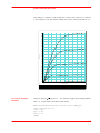
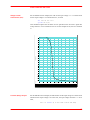
GETTING STARTED WITH HSPICE
Vbb 2 0 DC -2V
*Input Signal
*Vin 3 0 PWL 0ns 0V 0.4ns 5V 14.6ns 5V 0.4ns 0V
Vin 3 0 PULSE (0 5 0n 0.4n 0.4n 14.6n 30n)
*Inverter Circuit
M1 4 3 0 2 NENH L=2u W=4u AD=32p
M2 1 4 4 2 NDEP L=4u W=2u AS=32p
Cout 4 0 0.1pf
*Vout 4 0
*Include statement to obtain MOS model file
.INCLUDE "full_path_to_spice_model/nmos.3"
*
*For Voltage Transfer Characteristic (VTC)
.DC Vin 0 5 0.1
.PROBE DC V(4)
*For propagation delay and power
.TRAN 0.1ns 60ns
*For propagation delay
.PROBE TRAN V(3) V(4)
*For average power over one full Vin cycle
.MEAS TRAN avgpow AVG POWER FROM=30n TO=60n
.OPTIONS PROBE POST MEASOUT
.END
5
6
7
8
9
10
11
12
13
14
15
16
17
18
19
20
21
22
23
24
25
26
27
The first line of the SPICE file contains the name of the circuit. This line must always be
present. As in the second line, all lines beginning with an asterisk (*) are comments and
are optional. This file is more heavily commented than usual.
Lines 4 and 5 specify power supplies which are independent voltage sources. A voltage
source identifier always begins with V or v. In order to interconnect components, nodes
represented by integers are used. For example, Vdd is connected with its + terminal on
node 1 and its – terminal on node 0. Note that 0 is always used as the ground node. Vdd
is identified as a DC source with value +5V. The + and V are optional. This circuit is
somewhat unusual in that it has a substrate bias voltage Vbb ≠ 0 to give different circuit characteristics.
Vin in lines 7 and 8 is the input voltage to the circuit for transient analyses. Two alternative specifications, PWL (Piece-Wise Linear) and PULSE are given. The PWL specification begins with *; it is commented out and thus is not used although these two
specifications are identical for the first 30 ns. PULSE is useful for simple periodic waveforms such as clocks and PWL is useful for non-periodic waveforms. See the on-line
SPICE manual for the format of these waveform specifications.
Lines 10 and 11 describe the two MOSFETs in the inverter. The use of M# as the identifier designates a MOSFET. The order of the nodes is drain(D), gate(G), source(S) and
substrate(B). For example, node 4 is connected to the drain of M1 and to the gate and
source of M2. Next, NENH and NDEP give the name of the model for each of the transistors. The length L and width W of the channel of each device is given. The abbreviation
u designates “micro” which, for length in the MKS system, gives microns, µ. In addition, for transient analysis, the areas of the drain of M1 and the source of M2 are given.
The abbreviation p designates "pico" which is µ2. Line 12 specifies a capacitive load on
the inverter output of 0.1 pf. Line 15 includes the file nmos.3 containing the models
DIGITAL CIRCUIT SIMULATION USING HSPICE
3