1
Troubleshooting
2-49
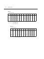
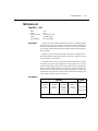
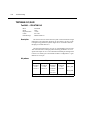
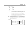
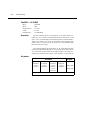
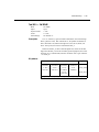
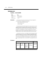
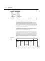
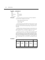
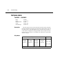
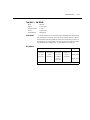
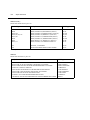
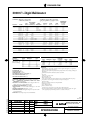
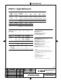
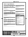
Test 403.1 — NON INV BEX2
Bank
Inputs
Expected Value
Limits
Fault Message
Description
VAC
Open
<none specified>
<none specified>
<none>
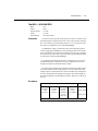
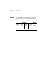
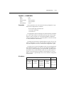
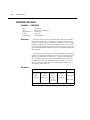
This test places the ACV front end in the non-inverting configuration.
Logic levels for this configuration are as follows:
K102: /SETK1 low, /RESETK1 high
U103: Pins 8 and 9 low
U105: Pin 9 high
The signal path is from ACIN through K102 to the plus input of U102. Resistors R117 (9.9MΩ) and R146 (1.1MΩ) to form a ÷10 at the input. The
feedback path for U102 is from the minus input through U103 (pins 6 and 7)
to node ACFE. The ACFE signal bypasses U112 through U103 (pin 16 low).
The signal is then coupled across C115 to U118 which is configured for x2
gain.
The output of U118 goes to U110 (TRMS converter) through the parallel
combination of R129, C113 and C114. The output of the TRMS converter
(OUT) is fed back through its own internal buffer. The buffer output signal
(BUFF OUT) is then labeled AC_MED. The AC_MED signal is selected at
U163 and fed to the A/D buffer (U166) through Q117. The A/D buffer is set
up for ×1 gain through U129 (/×1 low). This test is a setup phase for the next
test.
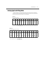
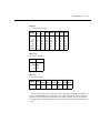
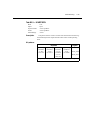
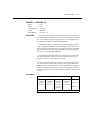
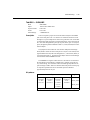
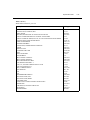
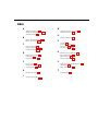
Bit patterns
Bit pattern
Q
Q
87654321
—U106—
011v0011
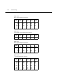
Q
Q
87654321
—U109—
11011111
Q
Q
87654321
—U134—
1v01000v
—U130—
10011101
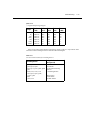
Register
Q
Q
87654321
—U121—
01110000
ACDC_STB
MUX_STB
IC pins: Q8=11, Q7=12, Q6=13, Q5=14, Q4=7, Q3=6, Q2=5, Q1=4