1
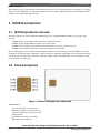
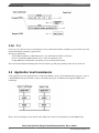
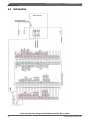
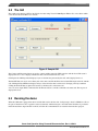
Freescale Semiconductor
Application Note
Document Number: AN4453
Rev. 0, 2/2012
Smart Card Operation Using
Freescale Microcontrollers
by:
Norman Guo
Contents
1 Introduction
1
Introduction................................................................1
This application note describes the operation fundamentals of
a smart card and how to use an MCU to communicate with it.
For ease of use, a graphic user interface (GUI) is provided as
an example.
2
ISO7816 Introduction...............................................2
This application note describes the operation fundamentals of
a smart card and how to use an MCU to communicate with it.
For ease of use, a graphic user interface (GUI) is provided as
an example.
There are many types of IC cards. The communication method
determines if the cards are contact cards or contactless
(wireless) cards. Implanted chips determine if the cards are
memory cards with only memory, or CPU cards which are
implanted with CPU. A CPU card, or smart card, has a CPU,
memory, and I/O on it. It runs a COS (Card Operating System)
to manage these resources. Different manufactures may adopt
different card operating systems.
3
This application note is based on a widely used CPU card
made by Watchdata. It is a contact type card running
TimeCOS. The ISO 7816 standard defines the necessary
protocols to communicate with a smart card. Although the
communication software is tested with TimeCOS, the basic
communication protocol (ISO 7816, T = 0) implemented in
this application note is common with all smart cards.
5
© 2012 Freescale Semiconductor, Inc.
4
2.1
ISO7816 protocols overview. . .......................2
2.2
Electrical interface.........................................2
2.3
Character frame.............................................3
2.4
Transmission level protocol...........................3
2.5
Application level transmission. .....................8
Smard Card COS.....................................................10
3.1
COS Introduction.........................................10
3.2
File System...................................................11
Hardware Circuit.....................................................12
4.1
Hardware Introduction.................................12
4.2
Schematics...................................................13
Software...................................................................15
5.1
Firmware.......................................................15
5.2
The GUI........................................................15
5.3
Running the demo........................................16
6
Conclusion...............................................................17
7
References...............................................................17
ISO7816 Introduction
This application note provides hardware circuit and software source codes for the card operation. A PC GUI is also provided,
and uses a specific USB driver to communicate with the smart card reader by USB. Integrated Circuit Cards Interface Device
(CCID) is not covered in this application note.
2 ISO7816 Introduction
2.1 ISO7816 protocols overview
The electric interface of contact cards and communication protocol are defined in ISO7816. Here are some parts of the
protocols:
•
•
•
•
ISO/IEC 7816-1 specifies physical characteristics for cards with contacts.
ISO/IEC 7816-2 specifies dimensions and location of the contacts.
ISO/IEC 7816-3 specifies electrical interface and transmission protocols for asynchronous cards.
ISO/IEC 7816-4 specifies organization, security and commands for interchange.
Because ISO7816 protocols use bi-directional, half-duplex transmission, the SCI module on Freescale MCUs can be easily
configured to fit. The SCI can be configured to a single-wire mode to implement a half-duplex serial connection with a smart
card. In this mode, the pin TxD is controlled by software as output or input. The TPM module can be configured to provide
the clock signal to the smart card.
2.2 Electrical interface
Figure 1. Position of the pads on a smart card
Signal definitions:
•
•
•
•
•
•
VCC: Power supply to the smart card.
RST: Reset signal goes into the smart card.
CLK: Clock signal goes into the smart card.
GND: Ground.
I/O: Bi direction signal for serial data.
RFU: Reserved for future use.
Smart Card Operation Using Freescale Microcontrollers, Rev. 0, 2/2012
2
Freescale Semiconductor, Inc.
ISO7816 Introduction
The cards are contained in three classes, based on operating voltage:
• Class A: 5 V
• Class B: 3 V
• Class C: 1.8 V
2.3 Character frame
One character is composed of 10 bits, and each bit is transmitted as I/O in one Elementary Time Unit (ETU). One ETU is
determined by the frequency of CLK (f), clock rate conversion integer (Fi), and baud rate adjustment integer (Di).
1 ETU = Fi / Di * (1/f)
Fi and Di are encoded in TAi (refer to Answer To Reset), default values are Fi=372, Di=1. If a 1.5 MHz CLK is used, by
default, 1 ETU = 372 / 1 * (1/1.5 MHz) = 248 us. You should configure the baud rate of the communication port as 4032 bps
(1/248 us).
The character is transmitted on the bidirectional I/O. Because it is a half-duplex channel, the reader and card cannot send data
at the same time. If there is a parity error in a byte transmission, the receiver shall send an error signal by pulling the I/O line
low at 10.5±0.2 ETU for duration of 1 to 2 ETU, which leads to a resend of the same data byte.
2.4 Transmission level protocol
When a smart card is inserted into the smart card reader and contacts are connected, the following procedures should be
conducted to operate and exchange information with it:
Activation: Activate the smart card. Receive Answer To Reset (ATR) information.
Exchange Information: Exchange information with the card based on T=0 (half-duplex transmission of characters) or T=1
(half-duplex transmission of blocks) protocol.
Deactivation: Deactivate the smart card.
The following sections contain more detailed descriptions.
2.4.1 Activation
When the reader detects the insertion of a card, it applies power to it. Refer to the following figure for a cold reset. The
minimum clock frequency f should be 1 MHz, and the maximum is 5 MHz. After RST is released to logic high, the ATR
should come from the card within a 400/f and 40000/f period of time. If the ATR does not come, the reader should apply a
deactivation.
Smart Card Operation Using Freescale Microcontrollers, Rev. 0, 2/2012
Freescale Semiconductor, Inc.
3
ISO7816 Introduction
2.4.2 Deactivation
The following figure should be followed to deactivate the smart card:
The reader should assert the RST first, then stop CLK, and finally, power off the smart card.
2.4.3 Answer To Reset
After cold reset, the reader will receive ATR, which has a maximum length of 33 bytes. The following table is a typical list of
the characters that should be included in ATR:
Table 1. Sample ATR
Characters
Initial character (mandatory)
TS
Format byte (mandatory)
T0
Description
Encodes Y1 and K
Table continues on the next page...
Smart Card Operation Using Freescale Microcontrollers, Rev. 0, 2/2012
4
Freescale Semiconductor, Inc.
ISO7816 Introduction
Table 1. Sample ATR (continued)
Characters
Interface bytes (optional)
Description
TA1
Encodes Fi and Di
TB1
Deprecated
TC1
Encodes N
TD1
Encodes Y2 and T
TA2
Specific mode byte
TB2
Deprecated
TC2
Specific to T=0
TD2
Encodes Y3 and T
...
TAi
TBi
TCi
TDi
Historical bytes (optional)
Encodes Yi+1 and T
T1
T2
...
Tk
Check byte (conditional)
TCK
Check character
Following is a brief introduction of these bytes. For more detailed descriptions, please refer to the protocol ISO-7816.
TS
The bits of a byte are transmitted on the I/O clocked by CLK, using either direct conversion or inverse conversion,
determined by TS. The TS has two possible patterns:
• HLHHLLLLLLH indicates an inverse convention. L presents bit 1, H presents bit 0. MSB transmitted first. In this case,
the SCI receives TS and decodes it as 0x3F.
• HLHHLHHHLLH indicates a direct convention. H presents bit 1, L presents bit 0. LSB transmitted first. In this case,
the SCI receives TS and decodes it as 0x3B.
T0
Y1 (Bit5 Bit6 Bit7 Bit8) indicates the presence of TA1 TB1 TC1 TD1. For example: Bit5 = 1 then TA1 present, Bit5 = 0
then TA1 absent. Bit6 is for TB1, Bit7 for TC1 and Bit8 for TD1.
K is the number of historical characters.
Smart Card Operation Using Freescale Microcontrollers, Rev. 0, 2/2012
Freescale Semiconductor, Inc.
5
ISO7816 Introduction
Interface bytes TAi, TBi, TCi, and TDi
Yi (Bit5 Bit6 Bit7 Bit8 of TDi) indicates the presence of TAi+1 TB i+1 TC i+1 TD i+1. If TDi is absent, then TAi+1 TBi+1 TCi+1
TDi+1 are all absent.
T (Bit4 Bit3 Bit2 Bit1 of TDi) is used to indicate a transmission protocol, qualify interface bytes. For example, T=0 refers to
the half-duplex protocol transmitting characters; T=1 refers to the half-duplex protocol transmitting blocks.
TAi TBi TCi encodes the clock rate conversion integer (Fi), the value of the baud rate adjustment integer (Di), the maximum
value of the frequency supported (f max), and extra guide time (N).
Historical bytes
These historical bytes T1,T2 to Tk provide the operating information of the card. If the first byte T1 is:
• 0x00: Indicates a status indicator in last three historical bytes.
• 0x10: Followed by DIR data reference.
• 0x80: Indicates a status indicator may present.
• 0x81 to 0x8F: Reserved for future use.
Any other value indicates a proprietary format.
TCK
This is a checksum byte formed by exclusive-oring all the bytes before TCK, starting from T0. If only T=0 is indicated, TCK
shall be absent.
2.4.4 Protocol and Parameters Selection (PPS)
Protocol and Parameters Selection (PPS) should be initiated by the reader, starting with PPSS (0xFF), followed by PPS0 and
optional PPS1, PPS2, and PPS3. With these proposed transmission protocol and parameters, the last byte is a checksum.
A successful response is also started with PPSS, followed PPS0, optional PPS1, PPS2, PPS3, and checksum byte. In most
cases, the response is the same as the PPS request. If the card does not support PPS or the reader uses the default parameters,
then PPS is not needed.
2.4.5 T=0
T=0 is a character level protocol. The process is always initiated by the reader by sending a command header, then waiting
for procedure bytes. According to the procedure bytes, the reader may send or receive the remaining optional data bytes, or
just receive the response status bytes.
Command Header
The command header includes five bytes: CLA, INS, P1, P2 and P3.
Smart Card Operation Using Freescale Microcontrollers, Rev. 0, 2/2012
6
Freescale Semiconductor, Inc.
ISO7816 Introduction
Code
Description
CLA
Class of command
INS
Instruction code
P1
Instruction parameters
P2
Instruction parameters
P3
Indicates the number of bytes to be transferred during the command
CLA indicates the class of command. If Bit8=0, then it is an inter industry class, else it is a proprietary class. Values 000x
xxxx and 01xx xxxx are commonly used classes.
The INS byte tells the card what to do. For example, 0xE0 means create file, 0xE4 means delete file and 0xD0 means write
binary.
P1, P2 are parameters for the command. For example, P1 P2 provide the file ID when executing a create file instruction.
P3 indicates the number of bytes to be transmitted. If the reader is sending data to the card, P3=0 means no data to be
transmitted. If the reader is reading data from the card, P3=0 means there are 256 bytes to be read.
Procedure bytes
After sending the command header, the reader will receive a procedure byte, before deciding what to do next.
If the byte is:
• 0x60, the reader deems it as a NULL byte and takes no action. Wait for a procedure byte.
• 0x6X except 0x60 or 0x9X, the reader deems it as the first status byte SW1 and takes no action. Wait for the second
status byte SW2.
• the same as the transmitted instruction byte INS, then it is an ACK byte. All remaining bytes should be transmitted. If
the value is the exclusive OR with sent INS, one remaining next byte should be transmitted.
Status bytes
In the last phase, the reader receives the status bytes SW1 and SW2. The following is a list of some typical status bytes:
• 0x9000: Command executed correctly.
• 0x61XX: SW2 encodes the number of bytes still available to be transmitted.
• 0x6E00: CLA not supported.
• 0x6D00: Instruction code not supported or invalid.
Please refer to ISO-7816 for more detailed descriptions.
Transmission Protocol Data Unit (TPDU)
The command header with its optional data bytes is named command TPDU. The response optional data bytes with
mandatory status bytes is named response TPDU. The following figure shows how the reader sends data to a smart card using
T=0 protocol.
Smart Card Operation Using Freescale Microcontrollers, Rev. 0, 2/2012
Freescale Semiconductor, Inc.
7
ISO7816 Introduction
2.4.6 T=1
For T=1 protocol, the basic unit to be transmitted is a block. A block frame includes a mandatory prologue field, an optional
information field and a mandatory epilogue field.
The epilogue includes the:
• Node Address (NAD) byte, which indicates the source and destination address of the block,
• Protocol Control Byte (PCB), which is used to control the transmission, and
• Length (LEN) byte, which indicates the number of bytes in the information field.
The content in the information field depends on the block frame type. The epilogue field provides an error check code.
2.5 Application level transmission
At the application level, the Application Protocol Data Unit (APDU) is used to send commands and get responses. A pair of
command APDU and response APDU is called a command-response pair. An APDU will be mapped to TPDU when
transmitting.
Refer to the following figure for the structure of the APDU frame. Please note the difference from the TPDU frame:
Smart Card Operation Using Freescale Microcontrollers, Rev. 0, 2/2012
8
Freescale Semiconductor, Inc.
ISO7816 Introduction
The header is four bytes (while the TPDU has five). The Lc field indicates the number of bytes in Data field, the Le field
indicates the expected number of bytes to be received. Normally the length of Lc and Le is one byte. Some cards explicitly
support extended fields of up to 3 bytes. There are four types of APDU command-response pairs:
Case 1: The command only has command header, no data field. The response only has trailer, no Data field.
Case 2: The command only has command header, no data field. The response has Data field and trailer.
Besides the normal response, the card may also respond:
• SW1:SW2 = 0x6700, which indicates the process aborted because the expected length Le is wrong;
• SW1:SW2 = 0x6CXX, which indicates the process aborted, Le was not accepted and a new length XX is indicated. The
reader shall issue the same command with XX;
• SW1:SW2 = 0x9XXX except 0x9000. SW1 and SW2 should be mapped to the response APDU without any change.
Smart Card Operation Using Freescale Microcontrollers, Rev. 0, 2/2012
Freescale Semiconductor, Inc.
9
Smard Card COS
Case 3: The command has command header and data field. The response only has trailer, no Data field.
Case 4: The command has command header and data field. The response has Data field and trailer.
After the reader issues the first TPDU with P3 = Lc, the response TPDU may be SW1:SW2 = 0x9000, as shown in the figure.
It is also possible to receive the following responses:
• SW1:SW2 with SW1 = 0x6X except 0x61, 0x62, 0x63. Indicates the process is aborted;
• SW1:SW2 with SW1 = 0x61, then SW2, which indicates the number of extra bytes available for retrieve. The reader
should use the INS = Get Response command with the smaller one of Le and SW2 to receive the data;
• SW1:SW2 = 0x62XX or 0x63XX or 0x9XXX except 0x9000. This response TPDU should be mapped to response
APDU without any change.
3 Smard Card COS
Smart Card Operation Using Freescale Microcontrollers, Rev. 0, 2/2012
10
Freescale Semiconductor, Inc.
Smard Card COS
3.1 COS Introduction
The Smart Card Operating System (COS) is a small operating system which resides in the smart card. It is similar to DOS
and Windows running on a PC, but much smaller and more specific. The following figure shows the typical structure of the
smart card:
The COS is stored in ROM, and CPU manages the transmission, stores the runtime command parameters, response, security
states, and temporary keys, in RAM. The application data is stored in EEPROM in a file format with security features
implemented. A COS has four functional modules:
Transmission management
The transmission management module receives commands and responds to the commands based on transmission protocol,
normally using ISO7816. T=0 is mandatory, and T=1 is optional. It should ensure the integrity of the transmission data.
Command interpreter
This module interprets the received commands and jumps to the appropriate function modules. After executing the
commands, it sends back status bytes indicating the result, and may also send back data as required.
Security control
The security module protects the card from unauthorized access. It can assign different levels of access rights for different
files.
File management
This module is responsible for organizing and managing the data stored in the card. Three types of files, which are Master
file (MF), Dedicated file (DF), and Elementary file (EF), are used to structure the file system.
3.2 File System
The application data is stored in the smart card in a file structure. There are three types of files:
• Master File (MF)
• Dedicated File (DF)
• Elementary File (EF)
Smart Card Operation Using Freescale Microcontrollers, Rev. 0, 2/2012
Freescale Semiconductor, Inc.
11
Hardware Circuit
Each card has only one MF, which is the root of the file system. The MF may contain DFs and EFs. A DF can be an
application DF that is hosting an application, or a parent that contains DFs. It can also contain zero or more EFs. The EF is
the unit to store application data. Each file has a unique identifier that can be used to select it. The MF has a reserved
identifier 0x3F00. It can be referenced directly anywhere in the file structure.
When compared with the DOS file system, MF is like the root directory, DF is like the directory and EF is like the file within
the directory.
The file can be operated by issuing APDU commands. For example, the command Read Binary can be used to read back the
contents of a specific file referenced by file ID.
APDU command for Read Binary EF: 00 B0 90 00 10:
• CLA 00: indicates it is an inter-industry class.
• INS B0: it is the ISO command code for binary file reading.
• P1 90: 0b10010000, bit8 is set to 1, which makes bit5 to bit 1 the short file ID 0x10.
• P2 00: read start from offset 00.
• Le 10: number of bytes expected to be returned.
4 Hardware Circuit
4.1 Hardware Introduction
The hardware circuit for the smart card reader is based on the demo board DEMOJM. The MCU is MC9S08JM60. SCI1 is
configured as single-wire mode, and TxD1 is used to communicate with the card’s I/O. In design practice, a parity error
rarely happens when an MCU communicates with a smart card, so the retransmission of a character on parity error is not
implemented in this example. TPM1 channel 0 is used to provide a clock to the card. All wires connected to the smart card
slot are from jumper J1.
Smart Card Operation Using Freescale Microcontrollers, Rev. 0, 2/2012
12
Freescale Semiconductor, Inc.
Hardware Circuit
•
•
•
•
•
•
PTE0/TxD1 is connected to I/O through a series resistor.
PTE2/TPM1CH0 is connected to CLK.
PTE3 is connected to RST.
VSS is connected to GND.
VDD goes through a transistor BC807 to the card’s VCC. The card’s power supply is controlled by PTG0.
PTG1/KBIP1 is connected to the normal open switch on the slot. When a card inserted into the slot, the switch will
close, which forces PTG1/KBIP1 to low. This is used to detect the insertion of a smart card.
The DEMOJM is configured in device mode. Please refer to its user manual for a detailed description of the configuration
and jumper settings.
Smart Card Operation Using Freescale Microcontrollers, Rev. 0, 2/2012
Freescale Semiconductor, Inc.
13
Hardware Circuit
4.2 Schematics
Smart Card Operation Using Freescale Microcontrollers, Rev. 0, 2/2012
14
Freescale Semiconductor, Inc.
Software
5 Software
5.1 Firmware
There are two main functional modules in the firmware. One is the USB module, which receives commands sent from the
PC, saves the APDU commands in the command buffer, and sets a flag of command received. In the main loop, when smart
card module finds this flag set, it will parse the APDU command, send it to the smart card, and get response from the smart
card. It then stores the optional response data and mandatory status bytes in response buffer. The USB module sends the
response back to the PC. Besides the control end point EP0, four end points are implemented:
Name
Direction
Type
Size (in bytes)
Description
EP1
Out
Interrupt
8
used to send a toggle data to the MCU periodically, to inform the
MCU the USB link is good. The MCU will toggle an LED when
receiving the toggling data.
EP2
In
Interrupt
8
used to inform the application software on the PC that events
occurred. In the example code, when the smart card is inserted or
removed from the slot, the application software on the PC will be
informed through this pipe.
EP3
Out
Bulk
64
used to send APDU commands to the MCU.
EP4
In
Bulk
64
used to send response APDU from smart card to PC.
The first byte in APDU command and response buffer is the length of the command or the response. For example, a pair of
command and response in the buffer may look like:
This is a command (Get Challenge) to get random data from the smart card. In the command buffer:
• 05 is the length of the command.
• 00 CLA
• 84 INS
• 00 P1
• 00 P2
• 04 Le
In the response buffer:
• 06 is the length of the response, including data and status bytes.
• 92, 87, FC, and 2D are the random data sent back by the smart card.
• 90 and 00 are the status bytes SW1 and SW2, and it means the command is executed correctly.
Smart Card Operation Using Freescale Microcontrollers, Rev. 0, 2/2012
Freescale Semiconductor, Inc.
15
Software
5.2 The GUI
The graphics user interface (GUI) on the PC side is written using Visual C# 2008 Express Edition. It is a free edition which
can be downloaded from Microsoft’s website.
Figure 2. Sample GUI
The Connect and Disconnect buttons are used to connect and disconnect the USB connection with the board. The status is
displayed in area 1. Area 2 displays whether the smart card is inserted in the slot or not.
Clicking the Get Challenge button displays 8 bytes of random data generated by the card, and is displayed in area 3.
The Read EF button is used to read a binary file on the smart card. The file ID is fixed to 0x10. The length of the file is 0x10
(16). Clicking the Read EF button displays 16 bytes of data from the smart card in area 4. Changing some bytes and then
clicking the Write EF button, updates the new data to the binary file on the smart card.
Area 5 is used to input APDU command. Click the Execute button to send the command to the smart card. The response is
displayed in area 6.
5.3 Running the demo
When the USB cable is plugged into the PC and the demo run for the first time, it will prompt to install a USB driver. Choose
the option “Install from a list or specific location (Advanced)” and then navigate to the folder where the driver is provided to
finish the installation. Open the GUI on the PC, and click the command buttons as needed for demonstration purposes.
Smart Card Operation Using Freescale Microcontrollers, Rev. 0, 2/2012
16
Freescale Semiconductor, Inc.
Conclusion
ISO7816 compatible commands can be executed. See the following list for examples. For more commands, refer to the
ISO7816 protocol.
• Get challenge (8 bytes): 00 84 00 00 08
• Get challenge (4 bytes): 00 84 00 00 04
• Select MF: 00 A4 00 00 02 3F 00
• Get Response: 00 C0 00 00 12
• Select ED: 00 A4 00 00 02 00 10
• Update binary: 00 D6 90 00 0A 00 11 22 33 44 55 66 77 88 99
6 Conclusion
This application note makes a brief introduction of ISO7816, and uses the SCI in single-wire mode to emulate the protocol. It
implements the basic communication protocol of ISO 7816 (T = 0), and provides some examples of inter-operation with
COS. Other commands can also be manually input on the GUI that can be sent to the smart card, and a response will be
displayed. The source codes are provided, and can be easily migrated to other MCUs such as the Kinetis family, which has
ISO7816 compatible UART.
7 References
Datasheet MC9S08JM60.
DEMOJMUM.
AC133 HandsonWorkshopHowToMakeaGraphicalUserInterfaceforYourUSBApplication.
Watchdata TimeCOS Reference Manual.
Smart Card Operation Using Freescale Microcontrollers, Rev. 0, 2/2012
Freescale Semiconductor, Inc.
17
How to Reach Us:
Home Page:
www.freescale.com
Web Support:
http://www.freescale.com/support
USA/Europe or Locations Not Listed:
Freescale Semiconductor
Technical Information Center, EL516
2100 East Elliot Road
Tempe, Arizona 85284
+1-800-521-6274 or +1-480-768-2130
www.freescale.com/support
Europe, Middle East, and Africa:
Freescale Halbleiter Deutschland GmbH
Technical Information Center
Schatzbogen 7
81829 Muenchen, Germany
+44 1296 380 456 (English)
+46 8 52200080 (English)
+49 89 92103 559 (German)
+33 1 69 35 48 48 (French)
www.freescale.com/support
Japan:
Freescale Semiconductor Japan Ltd.
Headquarters
ARCO Tower 15F
1-8-1, Shimo-Meguro, Meguro-ku,
Tokyo 153-0064
Japan
0120 191014 or +81 3 5437 9125
[email protected]
Asia/Pacific:
Freescale Semiconductor China Ltd.
Exchange Building 23F
No. 118 Jianguo Road
Chaoyang District
Beijing 100022
China
+86 10 5879 8000
[email protected]
For Literature Requests Only:
Freescale Semiconductor Literature Distribution Center
1-800-441-2447 or +1-303-675-2140
Fax: +1-303-675-2150
[email protected]
Document Number: AN4453
Rev. 0, 2/2012
Information in this document is provided solely to enable system and software
implementers to use Freescale Semiconductors products. There are no express or implied
copyright licenses granted hereunder to design or fabricate any integrated circuits or
integrated circuits based on the information in this document.
Freescale Semiconductor reserves the right to make changes without further notice to any
products herein. Freescale Semiconductor makes no warranty, representation, or
guarantee regarding the suitability of its products for any particular purpose, nor does
Freescale Semiconductor assume any liability arising out of the application or use of any
product or circuit, and specifically disclaims any liability, including without limitation
consequential or incidental damages. "Typical" parameters that may be provided in
Freescale Semiconductor data sheets and/or specifications can and do vary in different
applications and actual performance may vary over time. All operating parameters,
including "Typicals", must be validated for each customer application by customer's
technical experts. Freescale Semiconductor does not convey any license under its patent
rights nor the rights of others. Freescale Semiconductor products are not designed,
intended, or authorized for use as components in systems intended for surgical implant
into the body, or other applications intended to support or sustain life, or for any other
application in which failure of the Freescale Semiconductor product could create a
situation where personal injury or death may occur. Should Buyer purchase or use
Freescale Semiconductor products for any such unintended or unauthorized application,
Buyer shall indemnify Freescale Semiconductor and its officers, employees, subsidiaries,
affiliates, and distributors harmless against all claims, costs, damages, and expenses, and
reasonable attorney fees arising out of, directly or indirectly, any claim of personal injury
or death associated with such unintended or unauthorized use, even if such claims alleges
that Freescale Semiconductor was negligent regarding the design or manufacture of
the part.
RoHS-compliant and/or Pb-free versions of Freescale products have the functionality and
electrical characteristics as their non-RoHS-complaint and/or non-Pb-free counterparts.
For further information, see http://www.freescale.com or contact your Freescale
sales representative.
For information on Freescale's Environmental Products program, go to
http://www.freescale.com/epp.
Freescale™ and the Freescale logo are trademarks of Freescale Semiconductor, Inc.
All other product or service names are the property of their respective owners.
© 2012 Freescale Semiconductor, Inc.