1
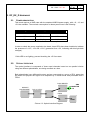
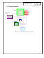
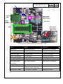
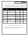
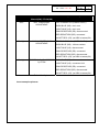
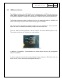
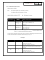
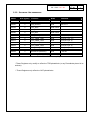
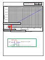
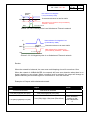
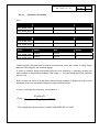
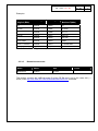
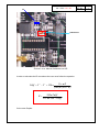
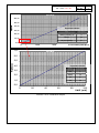
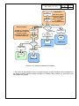
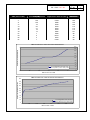
USER MANUAL
Function: Optical to RF
(DIGITAL)
Class: VME
PH/ESS document
No:
PH-ESS-02-01
Created :
11.10.2006
Modified:
date
Page
Rev.No.
1 of 29
1
RF_RX_D v1.0
Optical to RF Digital VMEbus Interface Card
and S/W
Summary:
This document describes the functionality of the RF_Rx_Digital card as well as the generic
S/W that has been developed for it.
Prepared by :
Checked by :
Approved by :
Markus Joos, PH/ESS
for information,
you can contact :
Tel.
Fax.
E-Mails
Markus Joos
+41.22.7672364
+41.22.7671025
[email protected]
Angel Monera
+41.22.7678925
+41.22.7678925
[email protected]
PH/ESS Document. No.
PH – ESS – ## – ##
Page
Rev. No.
2 of 29
1
Table of Contents
1.
Introduction ........................................................................................................................... 3
2.
RF_RX_D Hardware .............................................................................................................. 4
2.1.
Power description ........................................................................................................................ 4
2.2.
Optical Interface ........................................................................................................................... 4
2.2.1. Photodiodes Modules: .................................................................................................................................5
2.2.1.1.
Photodiode selection (Depending of the signal to transmit).................................................................7
2.2.1.2.
Photodiode configuration (Threshold and Selection) ...........................................................................7
2.2.1.3.
Signal Detection Circuit ........................................................................................................................9
2.2.2. Photodiodes Modules – Post processing Logic...........................................................................................9
2.2.2.1.
Frequency divider: ..............................................................................................................................10
2.2.2.2.
Output Format Selection.....................................................................................................................10
2.3.
VMEbus interface ....................................................................................................................... 11
2.3.1. Addr module sellection ..............................................................................................................................12
2.3.2. Software: Vme addres map .......................................................................................................................13
2.3.3. Registers Description.................................................................................................................................14
2.3.3.1.
EDA Identification ...............................................................................................................................14
2.3.3.2.
Signal Detection (only for ocp-srx) .....................................................................................................14
2.3.3.3.
VRef Registers (Only for TRR or equivalent photodiodes) ................................................................15
2.3.3.4.
Frequency Counters ...........................................................................................................................19
2.3.3.5.
Board Identification.............................................................................................................................20
2.4.
Calibration procedures (Trr or similar photodiode)................................................................ 21
2.4.1.
2.4.2.
2.4.3.
Manual Calibration (Fix Vref Values).........................................................................................................21
Through VME Knowing the Signals and Photodiodes used......................................................................24
Through VME Unknowing the Signals and Photodiodes...........................................................................24
2.5.
Board configuration- Jumpers and switch .............................................................................. 27
2.6.
Fibre / cable connections .......................................................................................................... 27
2.7.
Front-panel LEDs ....................................................................................................................... 28
2.8.
References or more information............................................................................................... 28
3.
TTC common software ....................................................................................................... 29
3.3.
3.3.1.
3.3.2.
Introduction ................................................................................................................................ 29
H/W Environment.......................................................................................................................................29
S/W Environment .......................................................................................................................................29
3.4.
Test programs ............................................................................................................................ 29
3.5.
The user library .......................................................................................................................... 29
PH/ESS Document. No.
PH – ESS – ## – ##
Page
Rev. No.
3 of 29
1
1. INTRODUCTION
The RF_RX_D (Optical to RF VMEbus card) is an interface VME card developed as receiver
of RF_TX_D VMEbus Interface card.
The two boards used together provide 3 digital optical channels, with an 1bit analog to digital
converter (comparator), and output LVPECL AC or DC coupled.
This document contains a hardware description of the board and all the accessible registers
of the RF_RX_D card as well as a description of the generic S/W that has been developed
for this card. At the end of this document, some basic examples of configuration procedures
are proposed.
PH/ESS Document. No.
PH – ESS – ## – ##
Page
4 of 29
Rev. No.
1
2. RF_RX_D HARDWARE
2.1.
POWER DESCRIPTION
This board requires a VME crate with the standard VME64 power supply, with +12, -12, and
+5 Volts available. The nominal consumption for these power lines is the following:
Voltage
Current (A)
Fuse Current
5V
2A
3A
+12V
150mA
0.5A
-12V
16mA
0.1A
Table 2.1: Power consumption
In order to check the power supplied to the board, three LEDs have been installed to indicate
the presence of +12V, -12V and +3.3V* (generated from +5V, indicating with this light both
voltages).
*If this LED is not lighting, proceed checking the +5V fuse state.
2.2.
OPTICAL INTERFACE
The optical interface is composed of three equal channels based on two parallel circuits
using two different photodiodes, one being mounted at a time.
Both photodiodes have differential output and are connected to a group of ECL gates that
will clean and prepare the signal to be amplified by a coaxial driver and processed with a
FPGA.
COAX DRIVER
MODULE
PHOTODIODE
SMA
CONNECTOR
PCL to LVPCL
FREQ
SPLITTER
FPGA
Picture 2.2: Optical Interface Diagram
PH/ESS Document. No.
PH – ESS – ## – ##
2.2.1. PHOTODIODES MODULES:
OCP
R
Power selector
Resistor
R
Truelight
Picture 2.2.1.a: Photodiodes Module in EDA 1380
Page
Rev. No.
5 of 29
1
PH/ESS Document. No.
PH – ESS – ## – ##
R
Truelight
(TRR)
Page
Rev. No.
6 of 29
1
TRR selector
(Disconnect
OCP selector)
Power
supply
selector
Inductance
OCP
OCP selector
(Disconnect
TRR selector)
Back side
Picture 2.2.1.b: important points in the board EDA 1382
Block
Signal
Vref Value
Light Green
OCP Place/ socket
Supported: Not adjustable
Dark Green
Truelight Place/ socket
Not supported
VIOLET UP RES.
3.3 Volts supply
Only one connected
VIOLET DOWN RES
5 Volts supply
Only one connected
PINK RESISTORS
Truelight signal selected
when 0R0 res. Are placed
RED RESISTORS
OCP signal selected
when 0R0 res. Are placed
BLUE RESISTORS
Resistor unbalancing the
Thevenin Network manually
when R /= 0R0 res.
BLUE INDUCTANCE
FPGA Control Thevenin
when placed (1uH)
(back side)
Table 2.2.1: Block description
PH/ESS Document. No.
Page
PH – ESS – ## – ##
2.2.1.1.
7 of 29
Rev. No.
1
PHOTODIODE SELECTION (DEPENDING OF THE SIGNAL TO TRANSMIT)
To the table below summarizes a review coming from the “Laser and Photodiodes
Evaluation” that shows the bandwidth and signal types that each Photodiode can receive.
For more information and characteristics, check the evaluation document or datasheets.
Photodiode
Bandwidth
Signal
Supported
Threshold
Thevenin
adjustable
10MHz square
YES
NO
Tb >10us
10KHz square
NO
NO
Freq > 300Mhz
5ns width 11Khz
(pulse)
Tb < 10us to 1ns
10MHz square
YES
NO
Freq: ~100 KHz to ~500 MHz
400MHz square
Tb > 10us
10KHz square
NO
NO
YES
YES
Positive
pulses YES
(maximum 16us
width)
YES
Example
OCP SRX 03
Time of bit (Tb) < 10us to 2ns
Freq: ~100 KHz to ~250 MHz
OCP SRX 03
OCP SRX 24
OCP SRX 24
5ns width 11Khz
(pulse)
Truelight
50KHz to 400Mhz
10MHz square
400MHz square
Truelight
Tb(high) < 16us
Table 2.2.1.1: Signals supported by each photodiode.
2.2.1.2.
PHOTODIODE CONFIGURATION (THRESHOLD AND SELECTION)
The table below shows a brief summary of the necessary adjusts that need to be done in
each channel to select the photodiode that is going to be used.
/
PH/ESS Document. No.
PH – ESS – ## – ##
Photodiode
Mode:
Page
8 of 29
Rev. No.
1
Components to replace
Manual(HW) / FPGA(SW)
OCP
NOT THRESHOLD
ADJUSTABLE
OCP CONNECTED (GREEN LIGHT)
DARK BLUE (DB) : don’t care
LIGHT BLUE (LB) : don’t care
PINK RESISTORS (PR): disconnected
RED RESISTORS (RR): connected
VIOLET RES. (VR): just 0R0 in bottom(5V)
Truelight
MANUAL THRESHOLD
ADJUSTABLE
TRUELIGHT CONN. (GREEN DARK)
DARK BLUE (DB) : 10ohms resistor
LIGHT BLUE (LB) : disconnected
PINK RESISTORS (PR): connected
RED RESISTORS (RR): disconnected
VIOLET RES. (VR): just 0R0 in bottom(5V)
Truelight
THRESHOLD ADJUSTABLE
by FPGA
DARK BLUE (DB) : 0ohms resistor
LIGHT BLUE (LB) : connected 1uH
PINK RESISTORS (PR): connected
RED RESISTORS (RR): disconnected
VIOLET RES. (VR): just 0R0 in bottom(5V)
Table 2.2.1.2: photodiode selection table
Insert examples pictures
PH/ESS Document. No.
PH – ESS – ## – ##
Page
Rev. No.
9 of 29
1
*******************************************************************************************
In case that another photodiode is going to be used, it has to be connected on:
−
OCP place if the Output format is pure PECL for all the bandwidth
−
TRUELIGHT place if the Output is differential NO PECL, with AGC in the last stage of
the preamplifier or with and internal AC coupled in the output.
In both cases the voltage must be selected between 3.3V and 5V with the Violet Resistors
*******************************************************************************************
*In FPGA mode VME FPGA who unbalances the Thevenin network. For this, it is necessary
write in the Vref Register a value different from 0. This makes it possible to unbalance the
network from ~0 to ~750mv.
2.2.1.3.
SIGNAL DETECTION CIRCUIT
The signal Detection circuit works ONLY with the OCP SRX photodiode. This circuit will
translate the signal detection state from the OCP to the Front panel.
A LED on the FP indicates the presence of optical power in each channel through a GREEN
light or the absence with a RED light.
In a future Firmware version signal detection for Truelight Photodiodes, based on the
frequency of the received signal, will be added. Meanwhile, the Frequency detectors
registers can be used to know the signal presence
2.2.2. PHOTODIODES MODULES – POST PROCESSING LOGIC
The post-processing logic is based on a few ECL gates that will increase the signal power in
order to drive the signal through long cables. The user will be able to choose the output
format between AC coupled 50 Ω or DC coupled LVPCL.
Another function of the Post Processing circuit is to split the signal and apply a frequency
divider with the objective to be able to monitor the frequency with the FPGA through the VME
interface.
PH/ESS Document. No.
Page
PH – ESS – ## – ##
Rev. No.
10 of 29
1
Output CAP:
AC/DC coupling selector
Picture 2.2.2: Photodiodes Post-Processing Logic
2.2.2.1.
FREQUENCY DIVIDER:
The Frequency Divider is composed of 5 Flip-Flops (FF) that divide the frequency by 16.
2.2.2.2.
OUTPUT FORMAT SELECTION
In order to select the format of the output (50Ω AC coupled ~800Vpp) or DC coupled
LVPECL, you must place in the output of the system a capacitor of 100 nf (AC) or a 0Ω
RESISTOR for DC coupling.
Insert picture capacitor output
Picture 2.2.2.2: Location of the Output Capacitor 0R0 Resistor
PH/ESS Document. No.
PH – ESS – ## – ##
2.3.
Page
Rev. No.
11 of 29
1
VMEBUS INTERFACE
The VMEbus interface of the RF_RX_D cards is implemented in its FPGA and based on a
VHDL Module developed by the AB/RF group. This Module has been developed especially
for VME64 but adapted for using some functionality of VME64X (like automatic addressing).
The firmware installed has been configured to work in the addressing mode of: A24/D16 and
works as a memory decoder, where all the memory space is available.
The access modes (dictated by address modifier) are only available for 0x39 and 0x3D,
where the there is no distinction between privilege user and normal user
From this 24bits of memory address, 6 bits are used for the module address [A23 to A18].
This address can be set up using the two rotary switches.
SW1
SW2
Picture 2.3: Module address selector
In addition, it is possible to fix automatically the module address by using the geographical
address of VME64x.
In order to select the source of the module address (rotary switches or GEO addr.), from the
8 bits of the R.S. the 2 lower bits are designated to select it.
PH/ESS Document. No.
Page
PH – ESS – ## – ##
Rev. No.
12 of 29
1
2.3.1. ADDR MODULE SELLECTION
Address space available:
Note:
M represent XXXX (any combination of 4 bits)
N represent XX (any combination of 2 bits)
0xM(N+0)0000 to 0xM(N+3) FFFF
Rotary Switch
1
Rotary
Switch 2
M
Bits(3:2)= N
Î 256 Kbytes of memory
Module address (MA)
Automatic GEO Address (5bits + 0)*
Bits(1:0)= “1 to
3”
M
[A23…A19] <= GEOGA(4 : 0)
A18 <= 0
Bits(3:2)= N
0xMN Manual Address
Bits(1:0)= “0”
[A23…A20] <= M
[A19…A18] <= N
*Requires VME64X crate
Table 2.3.1: Address and ADDR Mode selection
In others words, the bottom rotary switch (sw1) controls the addressing mode with the lower
two bits, which switches to automatic mode if the bit(0) or bit(1) = 1.
Examples:
Rotary Switch 1
Rotary Switch 2
0xF
0
Module MODO / ADDRESS / SPACE
Manual address
Module address: 0xF0 0000
Board space: 0xF00000 to 0xF3 FFFF
0xF
1
Automatic address
Module address: Depends on the slot into which the card
is plugged
0xF
4
Manual address
Module address: 0xF4 0000
Board space: 0xF40000 to 0xF7 FFFF
Table2.3.1.b: Examples of Module Addr
PH/ESS Document. No.
PH – ESS – ## – ##
Page
Rev. No.
13 of 29
1
2.3.2. SOFTWARE: VME ADDRES MAP
Offset
Size (bytes)
Function
Mode
Remarks
0x0000
2
EDA ID
Read
0x1382
0x0004
2
SIG_DETEC**
Read
bits 3 to 1
0x000A
2
CH1_REF*
Read / Write
0x000C
2
CH2_REF*
Read / Write
0x000E
2
CH3_REF
Read / Write
0x0010
2
CH1_FREQ_LOW
Read
Freq Ch1 (15..0)
0x0012
2
CH1_FREQ_HIGH
Read
Freq Ch1 (31..16)
0x0014
2
CH2_FREQ_LOW
Read
Freq Ch2 (15..0)
0x0016
2
CH2_FREQ_HIGH
Read
Freq Ch2 (31..16)
0x0018
2
CH3_FREQ_LOW
Read
Freq Ch3 (15..0)
0x001A
2
CH3_FREQ_HIGH
Read
Freq Ch3 (31..16)
0x003A
2
BOARD ID (CERN ID)
Read
0x016C
Others
Unused
Table 2.3.2: VME Memory Map
* These Registers only modify or affect the TRR photodiode (or any Photodiode placed in its
sockets)
** These Registers only affect the OCP photodiodes
PH/ESS Document. No.
Page
PH – ESS – ## – ##
14 of 29
Rev. No.
1
2.3.3. REGISTERS DESCRIPTION
2.3.3.1.
EDA IDENTIFICATION
Name
Offset
Size
Access
EDA ID
0x0000
16 bits
R
The EDA ID is just a register that can be used to identify the board. This default value is
0x1382, which correspond to the EDA number assigned to the project.
2.3.3.2.
SIGNAL DETECTION (ONLY FOR OCP-SRX)
Name
Offset
Size
Access
SIG_DETEC
0x0004
3 bits (3:1)
R
The register Signal Detect represents the signal detection in the OCP photodiodes (if there
are not OCP SRX installed, the value of this register can be false).
This register is connected to the front panel LEDs that indicate the signal presence with a
green light and no signal with red light.
For other photodiodes, use the frequency counters registers.
Examples:
Hex Value
SD in Ch 1
SD in Ch 2
SD in Ch 3
0x00
0x02
X
X
X
0x08
0x0A
X
0x0C
0x0E
Nothing: No signal
X
0x04
0x06
X: Signal Detected
X
X
X
X
X
X
X
Table 2.3.3.2: Signal detection combinations
PH/ESS Document. No.
PH – ESS – ## – ##
2.3.3.3.
Page
Rev. No.
15 of 29
1
VREF REGISTERS (ONLY FOR TRR OR EQUIVALENT PHOTODIODES)
These registers only work with the photodiodes plugged in the Truelight socket.
Name
Offset
Size
Access
Default
Values
CH1_REF
0x000A
8 bits
R/W
0x000A
CH2_REF
0x000C
8 bits
R/W
0x000A
CH3_REF
0x000E
8 bits
R/W
0x000A
CHX_REF are a group of register that control the previously mentioned Thevenin Network in
the 3 channels. The values of these registers will be sent to the DAC to modify the network.
The modification is linear and follows the equation:
Vdiff = V + − V − = 120 •
Voff (202 + R ) − Vcc • R
(202) • (202 + R )
Voff (mV ) = DACvalue * 4.7mV
Where:
Vdiff is the differential voltage between the differential lines
Voff is the DAC voltage value
R is the Manual Thevenin modifier
Supposing a R=0 we can obtain this graph where is possible to select graphically the value
for the register (the value is in Decimal, do not forget to change to hexadecimal)
PH/ESS Document. No.
Page
PH – ESS – ## – ##
800,00
Rev. No.
16 of 29
1
Vdiff
700,00
600,00
Vdiff (mV)
500,00
400,00
300,00
200,00
Optimal Value for Sinusoidal/Square signals (0x00)
100,00
0,00
50
0
Default value for everything (TRR)
100
150
200
Register Value (DEC)
Optimal value for pulse (TRR) (0x15)
Picture 2.3.3.3a : Vdiff variation with Vref_register
Positive
pulse
Vdiff
(0)
V-
Output
V+
Reference for BOTH LINES
Negative
pulse
Noise when low level is keep more than 10us
Picture 2.3.3.3b: Positive pulse in balanced Thevenin network
250
PH/ESS Document. No.
Page
PH – ESS – ## – ##
Positive
pulse
V-
17 of 29
Rev. No.
1
New reference for Negative
Line (Controlled by VME)
Theoretical reference for BOTH LINES
Vdiff
V+
New reference for Positive Line (Controlled by
hardware – Resistor -
Out
Pulse width reduced
Picture 2.3.3.3c: Positive pulse in an Unbalanced Thevenin network
V-
New reference for Negative Line
(Controlled by VME)
Negative
pulse
Vdiff
V+
Out
No cross NO signal
Theoretical reference for both LINES
New reference for Positive Line
(Controlled by hardware – Resistor -
Picture 2.3.3.3d: Negative pulse in an Unbalanced Thevenin network
Review:
When the network is balanced, the user must avoid keeping a level for more than 10us.
When the network is UNBALANCED, the network will force zero detection when there is no
signal, negative or zero signal. When a positive level is received, the output will change to
positive following the received signal for a maximum of 10us will received.
Examples of Outputs with unbalanced network:
Input
Output
notes
Low level 50 seconds
Low level 50 seconds
Low (50s) high(5us) low (50s)
Low (50s) high(5us) low (50s)
Low (50s) high(50us) low (50s)
Low (50s) high(~10us) low (50s+ 40us)
AGC actuation,
setting up the
level received to
0
PH/ESS Document. No.
PH – ESS – ## – ##
Page
Rev. No.
18 of 29
1
Examples of VREF adjustment:
Supposing just FPGA modification (R=0), the Vdiff can vary from 0 to 0.71Vots (Voff = .2V
(0xFF in the Vref Register))
The Comparator used (ADCPM553) nees, at least, 10mv of differential voltage between its
inputs. If we don’t want the comparator to oscillate, we need to fix the Vdiff voltage in at
least 20/30mV (minimum voltage + some more for noise immunity). Then, the value to write
in the register (following the equations or the graph) is 0x0A.
This value ensures the reception of all the signals with all the receivers but is not optimised.
Note: any value different from 0 will generate duty cycle distortion in the high frequency
signals. The user must decide what he exactly needs and set up these values as convenient
is for him.
Insert pictureeeeeeeeeeeeeeeeeeeeeeeeeee
PH/ESS Document. No.
Page
PH – ESS – ## – ##
2.3.3.4.
Rev. No.
19 of 29
1
FREQUENCY COUNTERS
CH1
Name
Offset
Size
Access
CH1_FREQ_LOW
0x0010
16 bits
R
CH1_FREQ_HIGH
0x0012
16 bits
R
Name
Offset
Size
Access
CH2_FREQ_LOW
0x0014
16 bits
R
CH2_FREQ_HIGH
0x0016
16 bits
R
Name
Offset
Size
Access
CH3_FREQ_LOW
0x0018
16 bits
R
CH3_FREQ_HIGH
0x001A
16 bits
R
CH2
CH3
These registers are generated by internal counters that count the number of rising clocks
between rising edges in the received signals.
In order to measure higher frequencies than the clock frequency, a frequency divider has
been installed on the board (4 hardware Flips-Flops = > 1/16) and inside the FPGA (software
divider 1/22)
Every counter has a size of 32 bits that is divided in two registers of 16bits that must be read
separately due to the fact that the board has only A24/D16 access.
In order to calculate the frequency, the equation is:
Freq =
80 • 16 • 22
Re gLow + Re gHigh • 65536*
* This multiplication must be done in LONG UNSIGNED INT or FLOAT
PH/ESS Document. No.
Page
PH – ESS – ## – ##
Rev. No.
20 of 29
1
Examples:
Frequency
Original (MHz)
ValueReg1
Value Reg2
Frequency
Measured (MHz)
10
0x0000
0x0B00
10
40.078
0x0000
0x02BF
40.0568
0x0000
0x02BE
40.113
0x0000
0x0047
396.619
0x0000
0x0046
402.285
Pulse 1MHz
0x0000
0x6e00
1MHz
Pulse 11.245KHz
0x0026
0x361A
11.245027KHz
No signal
0xFFFF
0xFFFF
6Hz
400.78
Table 2.3.3.4 : Typical examples of values of the frequency counter
2.3.3.5.
BOARD IDENTIFICATION
Name
Offset
Size
Access
BOARD ID
0x003A
16 bits
R
This register contains the VME64x board ID of the RF-RX and is set to the value 364 ( =
0x16C). See http://ess.web.cern.ch/ESS/boardIDistribution/PHP/ for details
PH/ESS Document. No.
PH – ESS – ## – ##
2.4.
Page
Rev. No.
21 of 29
1
CALIBRATION PROCEDURES (TRR OR SIMILAR PHOTODIODE)
The calibration procedure will apply only to the channels where a TRUELIGHT or equivalent
photodiode is installed.
The OCP photodiodes DO NOT REQUIRE ANY CALIBRATION. Only be
selected (see section 2.2.1.1)
The calibration procedure can be done manually or trough VME, dividing this last option in
two different scenarios.
Knowing the frequency and type of the signal received
Unknowing the frequency and type of the signal received
In order to read and modify the board’s registers the program rfrxscope * has been
developed. It helps the user accessing the board registers in an interactive way.
* rfrxscope has been written by Markus Joos.
2.4.1. MANUAL CALIBRATION (FIX VREF VALUES)
This configuration will be applied when a VME controller is not present or block the
references to avoid third part modifications or intromission.
The manual modification is done by modifying the Resistors R and disconnecting/desoldering the inductance (more information about full Truelight Set UP in section 2.2.1)
PH/ESS Document. No.
Page
PH – ESS – ## – ##
R
Rev. No.
Inductance
Picture 2.4.1a: Manual Calibration set UP
In order to calculate the R convenient the user must follow the equation:
Vdiff = V + − V − = 120 •
R=
Or the next Graphs:
Vcc • R
(202) • (202 + R )
202 • Vdiff
Vcc • 0.594 − Vdiff
22 of 29
1
PH/ESS Document. No.
Page
PH – ESS – ## – ##
70,0
23 of 29
Rev. No.
1
R/Vdiff
60,0
R(ohm
s)
50,0
40,0
Important values:
30,0
Freq
R in Ohms
20,0
>1MHz (centred in 0)
0
10,0
Pulses
3.5
All (not optimal)
2.1
0,0
0
200
7,0
400
600
800
Vdiff (mV)
R/Vdiff
6,0
R(ohms)
5,0
4,0
Important values:
3,0
2,0
1,0
Vdiff
R in Ohms
0mV
0
20mV
1.4
30V
2.1
50V
3.5
0,0
0
20
40
60
Pictures 2.4.1b: Calibration Graphs
80
100
Vdiff (mV)
PH/ESS Document. No.
PH – ESS – ## – ##
Page
24 of 29
Rev. No.
1
2.4.2. THROUGH VME KNOWING THE SIGNALS AND PHOTODIODES USED.
The calibration can be done with monitor software like rfrxscope (By Markus Joos) or with
readRXD monitor (Tcl application that run over Markus Joos Vme_Drivers).
If the user is close to the board and knows the type of receivers that are mounted and which
signal type they are receiving.
Then, apply these rules
Photodiode
Signal
Vref Value
OCP SRX 03
1Mhz to 100Mhz clocks
No adjustment required
OCP SRX 03
400Mhz or Pulses clocks
Don’t care – Not supported
OCP SRX 24
1Mhz to 500Mhz clocks
No adjustment required
OCP SRX 24
Pulses
Don’t care – Not supported
Truelight
0.5Mhz to 400Mhz clocks
Required: 0x00
Truelight
Pulses
Required: 0x15
Truelight
Any (not optimal)
Required: 0x0A
Table 2.4.2: Manual Calibration Values
2.4.3. THROUGH VME UNKNOWING THE SIGNALS AND PHOTODIODES
This will be the procedure (algorithm) to apply when the user doesn’t know what types or
receivers are installed in the board and which types of signals are received.
Like in the same procedure, VME access software will be required in order to read and
modify the desired registers.
PH/ESS Document. No.
Page
PH – ESS – ## – ##
This value works
with all the signals
with an optical
power from 0dbm
to -26dbm
(Not Optimal Value)
Wait 54
secs
If there is a Truelight Write 0xFF
with NO pulse, this will
block the signal,
revealing the OCP if we
Wait 54
continue Receiving
secs
Write 0x0A
10Hz<F<100Khz
Frequency
?
Blocking signal:
F > 10Hz
1
Initialization:
Start
Write 0x0A
F>100Khz
Rev. No.
25 of 29
<10Hz or
0XFFFF FFFF
NO SIGNAL
END
END
Frequency
?
<10Hz or
0XFFFF FFFF
Write 0x3A**
(TRUELIHT)
(TRUELIHT)
Write 0x00
END
OCP
END
(TRUELIHT)
Picture 2.4.3: Remote Calibration Procedure
** This value is the minimum value to accept the pulse in good conditions and correspond to
the worst scenario possible (signal reception at -27dBm). More values can be found in the
next tables and graphs
PH/ESS Document. No.
Page
PH – ESS – ## – ##
Power Received in
dBm (5.6ns width)
-5
-7
-9
-11
-13
-15
-17
-19
-21
-23
-25
-27
Rev. No.
Value Hex for obtain a
output Pulse widh of 5,6ns
0xB5
0XA0
0X88
0X78
0X70
0X70
0X70
0X65
0X58
0X4C
0X44
0X3A
Pw (uW)
316
199
125
79
50
31
19
12
7
5
3
1
26 of 29
1
Value Dec
181
160
136
120
112
112
112
101
88
76
68
58
TRR V reference value for Pulse transmision
200
Vref Value por input/output pulse 5,7V
180
160
140
120
100
80
60
40
Tx Configuration Ch3 with Vref
0x70 (560mv) 5,6ns width pulse
20
0
-30
-25
-20
-15
-10
0
-5
dBm received in TRR
TRR V reference value for Pulse transmision
200
Vref Value por input/output pulse 5,7V
180
160
140
120
100
80
60
40
Tx Configuration Ch3 with Vref
0x70 (560mv) 5,6ns width pulse
20
0
0
50
100
150
200
uW received in TRR
250
300
350
PH/ESS Document. No.
PH – ESS – ## – ##
2.5.
Page
27 of 29
Rev. No.
BOARD CONFIGURATION- JUMPERS AND SWITCH
Element
Description
LSB rotary switch
See 2.3.1 section
MSB rotary switch
See 2.3.1 section
Reset(Front Panel)
button
Generate a Soft reset of the FPGA when is pressed
ST5
Always OFF
ST4
Always ON
TP25
Frequency selector0 for the JTAG
TP26
Frequency selector1 for the JTAG
ST3
If ST3 is ON -> the FPGA will be reprogrammed when the VME
crate reset will be activated (triggered by a VMEbus SYSRESET)
Table 2.5: Jumpers and Switch descriptions
2.6.
FIBRE / CABLE CONNECTIONS
Connector name
To be connected to
Format
CH1 IN Optical Link
RF Digital TX
Optical (Digital or Analog)
CH1 RF Out
50omhs LOAD
LVPECL 50ohms AC/DC coupled
CH2 IN Optical Link
RF Digital TX
Optical (Digital or Analog)
CH2 RF Out
50ohms LOAD
LVPECL 50ohms AC/DC coupled
CH3 IN Optical Link
RF Digital TX
Optical (Digital or Analog)
CH3 RF Out
50ohms LOAD
LVPECL 50ohms AC/DC coupled
J5
JTAG
JTAG MODE (FPGA)
J6
JTAG
BIT BLASTER MODE (EEPROM)
Table 2.6: Connectors and Descriptions
1
PH/ESS Document. No.
PH – ESS – ## – ##
2.7.
Page
Rev. No.
28 of 29
1
FRONT-PANEL LEDS
LED
Description
VME COMM
Indicates if the last VME cycle was successful or wrong
ERROR LED
Indicates an error in ?????
CH1 LED (SD CH1)
Indicates Optical signal (only OCP*) when is receiving >-30dbm
CH2 LED (SD CH2)
Indicates Optical signal (only OCP*) when is receiving >-30dbm
CH3 LED (SD CH3)
Indicates Optical signal (only OCP*) when is receiving >-30dbm
Table 2.7: Front Panel LEDS
*Possible modification in the definitive board for signal detection based in the Frequency
detection valid for all photodiodes.
2.8.
REFERENCES OR MORE INFORMATION
Lasers and Photodiodes evaluation (by Angel Monera)
EDA documents (https://edms.cern.ch/nav/eda-01382)
RF_RX_D TCL console Manual
RF_TX_D User Manual
PH/ESS Document. No.
PH – ESS – ## – ##
3.
TTC COMMON SOFTWARE
3.3.
INTRODUCTION
3.3.1. H/W ENVIRONMENT
3.3.2. S/W ENVIRONMENT
3.4.
TEST PROGRAMS
3.5.
THE USER LIBRARY
Page
Rev. No.
29 of 29
1