1
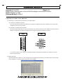
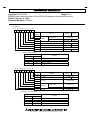
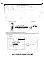
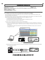
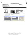
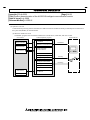
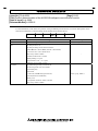
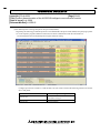
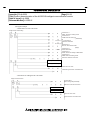
TECHNICAL BULLETIN
[Issue No.] FA-A-0059
[Page] 1/22
[Title] Product discontinuation of the A1SD51S intelligent communication module
[Date of Issue] July 2009
[Relevant Models] A1SD51S
Thank you for your continued support of Mitsubishi programmable controllers, MELSEC series.
Production of the following MELSEC-AnS series model will be discontinued.
1. Model to be discontinued
Product name
Model
A1SD51S Intelligent communication module
A1SD51S
2. Schedule
y Transition to made-to-order production: December 31, 2009
y Order acceptance:
Through May 31, 2010
y Production discontinuation:
June 30, 2010
3. Reasons for discontinuing production
Some parts of the above product are now obsolete. Therefore, we will have difficulty to maintain the production system.
4. Repair acceptance
y Repair acceptance: Through June 30, 2017 (For 7 years after production discontinuation)
5. Alternative models
Discontinued model
A1SD51S
Alternative model*1
y QD51 (RS-232: 2 channels)
y QD51-R24 (RS-232: 1 channel, RS-422/485: 1 channel)
To replace the discontinued model with the QD51 or QD51-R24, transition to a MELSEC-Q series system is required.
Note that MELSEC-AnS series modules can be utilized on MELSEC-Q series systems by using extension base units
QA1S6 B.
For use of the QA1S6 B, applicable CPU and other module models are restricted.
For details, refer to the QCPU User’s Manual (Hardware Design, Maintenance and Inspection).
*1 In some applications, a computer link module (A1SJ71UC24-R2/R4/PRF) or a serial communication module
(QJ71C24N(-R2/R4)) can be used as an alternative.
For details, refer to “9. No-protocol mode of a computer link module (A1SJ71UC24-R2/R4/PRF)” or “10. Pre-defined
protocol function of the serial communication module (QJ71C24N(-R2/R4)).
HEAD OFFICE : TOKYO BUILDING, 2-7-3 MARUNOUCHI, CHIYODA-KU, TOKYO 100-8310, JAPAN
NAGOYA WORKS : 1-14, YADA-MINAMI 5-CHOME, HIGASHI-KU, NAGOYA, JAPAN
TECHNICAL BULLETIN
[Issue No.] FA-A-0059
[Page] 2/22
[Title] Product discontinuation of the A1SD51S intelligent communication module
[Date of Issue] July 2009
[Relevant Models] A1SD51S
6. Differences in performance specifications between the A1SD51S and the QD51(-R24)
The following table shows differences in performance specifications.
Item
A1SD51S
QD51
Input: 27 points
General input/output
programmable controller CPU)
Interface
Input: 26 points
Output: 23 points
(2 points: For task start from the
QD51-R24
Output: 23 points
(2 points: For task start from the programmable controller CPU)
RS-232
2 channels (D-sub 9-pin)
2 channels (D-sub 9-pin)
RS-422/485
1 channel (D-sub 25-pin)
-
Power failure protection
Yes
1 channel (D-sub 9-pin)
1 channel
(Two-piece terminal block)
None
Refer to “8. (3) (c) Common memory reading and writing”.
A7PHP, A7HGP, A7LMS,
Console
VG-620, VT-382,
PC/AT personal computer
PC/AT personal computer
HEAD OFFICE : TOKYO BUILDING, 2-7-3 MARUNOUCHI, CHIYODA-KU, TOKYO 100-8310, JAPAN
NAGOYA WORKS : 1-14, YADA-MINAMI 5-CHOME, HIGASHI-KU, NAGOYA, JAPAN
TECHNICAL BULLETIN
[Issue No.] FA-A-0059
[Page] 3/22
[Title] Product discontinuation of the A1SD51S intelligent communication module
[Date of Issue] July 2009
[Relevant Models] A1SD51S
7. Replacement procedure
The following is the procedure for replacing the A1SD51S with the QD51(-R24).
START
Connect a console and an external device to the QD51(-R24).
8(1) Connecting a console and an external device to the QD51(-R24)
Connect GX Developer to the CPU module.
In GX Developer, configure the intelligent function module switch
settings for the QD51(-R24).
Set Switch 2 to 0004H (Programming mode).
8(2) Setting the mode
Modify the BASIC program that has been used for the A1SD51S.
8(3) Modifying the BASIC program used for the A1SD51S
Modify the sequence program.
8(4) Modifying the sequence program
Debug the programs.
In the QD51(-R24) intelligent function module switch setting
dialog box of GX Developer, change the Switch 2 value to any
of 0000H to 0003H (Run mode or Multitask debug mode).
8(2) Setting the mode
END
HEAD OFFICE : TOKYO BUILDING, 2-7-3 MARUNOUCHI, CHIYODA-KU, TOKYO 100-8310, JAPAN
NAGOYA WORKS : 1-14, YADA-MINAMI 5-CHOME, HIGASHI-KU, NAGOYA, JAPAN
TECHNICAL BULLETIN
[Issue No.] FA-A-0059
[Page] 4/22
[Title] Product discontinuation of the A1SD51S intelligent communication module
[Date of Issue] July 2009
[Relevant Models] A1SD51S
8. Replacing the A1SD51S with the QD51(-R24)
(1) Connecting a console and an external device to the QD51(-R24)
(a) Connection to the RS-232 interface
Since the same RS-232 interface specifications are applied to the QD51(-R24) and the A1SD51S, the existing cable
and RS-232 converter can be reused.
(b) Connection to the RS-422/485 interface
Because the QD51(-R24) uses a two-piece terminal block, the existing connector for the A1SD51S cannot be reused. In
addition, wiring must be checked and changed since the signals are assigned to different positions.
For connection details, refer to the Q Corresponding Intelligent Communication Module User’s Manual, “RS-232
Interface Specifications”.
(2) Setting the mode
The mode of the QD51(-R24) is set in the intelligent function module setting dialog box of GX Developer while the mode
of the A1SD51S is set with the mode setting switch on the module.
HEAD OFFICE : TOKYO BUILDING, 2-7-3 MARUNOUCHI, CHIYODA-KU, TOKYO 100-8310, JAPAN
NAGOYA WORKS : 1-14, YADA-MINAMI 5-CHOME, HIGASHI-KU, NAGOYA, JAPAN
TECHNICAL BULLETIN
[Issue No.] FA-A-0059
[Page] 5/22
[Title] Product discontinuation of the A1SD51S intelligent communication module
[Date of Issue] July 2009
[Relevant Models] A1SD51S
(a) Switch 1
b7 b6 b5 b4 b3 b2 b1 b0
Bit
Contents
position
b0
b1
Console
b3
Not used
b4
Console, debugger type
b5
Ctrl + C setting
b6
Not used
Access possible time setting after Y reset
b7
ON(1)
Refer to *1
Channel setting
Software
b2
OFF(0)
Not used
Used
Fixed on OFF
VT
VG
Disabled
Enabled
Fixed on OFF
200 ms
2000 ms
OFF(0)
ON(1)
*1 Console (Channel setting)
Bit position
Contents
b1
b0
OFF
OFF
Without console
OFF
ON
With console CH.1
ON
OFF
With console CH.2
ON
ON
Setting impossible
bF bE bD bC bB bA b9 b8
Bit
Contents
position
b8
Not used
b9
Flash ROM write protection setting
bA
bB
Not used
bC
bD
Debugger
bE
bF
Fixed on OFF
Without
With
Fixed on OFF
Channel setting
Software
Refer to *2
Not used
Not used
Fixed on OFF
*2 Debugger (Channel setting)
Bit position
Contents
bD
bC
OFF
OFF
Without a debugger
OFF
ON
With debugger CH.1
ON
OFF
With debugger CH.2
ON
ON
Setting impossible
Used
HEAD OFFICE : TOKYO BUILDING, 2-7-3 MARUNOUCHI, CHIYODA-KU, TOKYO 100-8310, JAPAN
NAGOYA WORKS : 1-14, YADA-MINAMI 5-CHOME, HIGASHI-KU, NAGOYA, JAPAN
TECHNICAL BULLETIN
[Issue No.] FA-A-0059
[Page] 6/22
[Title] Product discontinuation of the A1SD51S intelligent communication module
[Date of Issue] July 2009
[Relevant Models] A1SD51S
(b) Switch 2
Set value
Description
0000H
0001H
0002H
0003H
0004H
0005H to 000FH
Remark
Run mode
Mode for executing the BASIC program.
Multitask debug mode
Mode for debugging by connecting a debugger.
Programming mode
Mode for programming by connecting a console.
Setting prohibited
-
(c) Switch 3 to Switch 5
Set 0000H.
(3) Modifying the BASIC program used for the A1SD51S
Programs used for the A1SD51S can be utilized for the QD51(-R24).
However, modification of the BASIC program may be required since the following setting items may be different between
these models.
(a) Channels
Available channels differ for each model of the QD51(-R24).
If a channel not available for the QD51(-R24) has been used on the A1SD51S, modify the BASIC program and change
the channel setting.
Item
A1SD51S
QD51
QD51-R24
CH.1 (RS-232)
CH.2 (RS-232)
CH.3 (RS-422/485)
: Available,
(b) Data bit and stop bit
The data bit and stop bit settings differ.
Correct the BASIC program.
Item
A1SD51S
QD51
QD51-R24
Data bit
5, 6, 7, 8
7, 8
Stop bit
1, 1.5, 2
1, 2
HEAD OFFICE : TOKYO BUILDING, 2-7-3 MARUNOUCHI, CHIYODA-KU, TOKYO 100-8310, JAPAN
NAGOYA WORKS : 1-14, YADA-MINAMI 5-CHOME, HIGASHI-KU, NAGOYA, JAPAN
: N/A
TECHNICAL BULLETIN
[Issue No.] FA-A-0059
[Page] 7/22
[Title] Product discontinuation of the A1SD51S intelligent communication module
[Date of Issue] July 2009
[Relevant Models] A1SD51S
(c) Common memory reading and writing
The common memory of the QD51(-R24) is not backed up with a battery.
If a backup is needed, use the file register (R) in a programmable controller CPU.
In that case, change the part for accessing the common memory with the GETMEM and PUTMEM commands to the
part for accessing the file register (R) with the PCRD and PCWT commands.
(d) PCRD and PCWT commands
The following processing codes for the A1SD51S cannot be executed for QCPUs and QnACPUs.
For processing available for the alternative, change the processing code.
(PCRD command)
Processing codes for the A1SD51S
Processing
Description
Code
2(&H2)
4(&H4)
5(&H5)
7(&H7)
8(&H8)
9(&H9)
Reading of expansion file register data
Monitoring the expansion file register
515(&H203)
Reading of Q/QnA series device memory
monitor registered by the PCWT command
Reading of continuous address designation
data in the expansion file register
Reading of sequence programs
Reading of microcomputer programs
11(&HB)
Reading of expansion comment data
14(&HE)
Description
Code
the PCWT command
Reading of comment data
13(&HD)
Processing
Monitoring of the device monitor register by
10(&HA)
12(&HC)
Processing codes for the QD51(-R24)
Reading of the special function module buffer
memory
Reading of programmable controller CPU
model name
-
533(&H215)
513(&H201)
Not available for the Q/QnA series.
Reading of Q/QnA series intelligent function
module buffer memory
Reading of Q/QnA series programmable
controller CPU model name
Reading of parameter data(Reading of
MELSECNET/10 parameters)
21(&H15)
Reading of network information
22(&H16)
Reading of routing parameters
-
Not available for the Q/QnA series.
HEAD OFFICE : TOKYO BUILDING, 2-7-3 MARUNOUCHI, CHIYODA-KU, TOKYO 100-8310, JAPAN
NAGOYA WORKS : 1-14, YADA-MINAMI 5-CHOME, HIGASHI-KU, NAGOYA, JAPAN
TECHNICAL BULLETIN
[Issue No.] FA-A-0059
[Page] 8/22
[Title] Product discontinuation of the A1SD51S intelligent communication module
[Date of Issue] July 2009
[Relevant Models] A1SD51S
(PCWT command)
Processing codes for the A1SD51S
Processing
Description
Code
2(&H2)
Device memory monitor registration
3(&H3)
Random writing to device memory
4(&H4)
Writing to expansion file register
5(&H5)
Expansion file register monitor registration
6(&H6)
Random writing to expansion file register
7(&H7)
8(&H8)
9(&H9)
515(&H203)
Writing to Q/QnA series device memory
Writing of sequence program
Writing of microcomputer program
11(&HB)
Writing of expansion comment data
15(&HF)
Description
Code
to expansion file register
Writing of comment data
14(&HE)
Processing
Continuous address designation data writing
10(&HA)
12(&HC)
Processing codes for the QD51(-R24)
Writing to special function module buffer
memory
-
533(&H215)
Not available for the Q/QnA series.
Writing to Q/QnA series intelligent function
module buffer memory
Writing of parameter data (Writing of
MELSECNET/10 parameters)
-
Not available for the Q/QnA series.
Analysis of parameter data
HEAD OFFICE : TOKYO BUILDING, 2-7-3 MARUNOUCHI, CHIYODA-KU, TOKYO 100-8310, JAPAN
NAGOYA WORKS : 1-14, YADA-MINAMI 5-CHOME, HIGASHI-KU, NAGOYA, JAPAN
TECHNICAL BULLETIN
[Issue No.] FA-A-0059
[Page] 9/22
[Title] Product discontinuation of the A1SD51S intelligent communication module
[Date of Issue] July 2009
[Relevant Models] A1SD51S
(e) DATE$ function
Modify the BASIC program since the DATE$ function processing is different between the discontinued and alternative
models.
Processing
A1SD51S
QD51(-R24)
Action
Reads only the last two digits of
the year.
If the last two digits are 90 or
Reading
more, the first two digits are 19. If
Reads the four-digit year as it is.
Modify the program to use
four-digit year processing.
the last two digits are less than 90,
the first two digits are 20.
Writes only the last two digits of
Writing
the year.
Writes the four-digit year as it is.
Designate the year as four digits
correctly.
(4) Modifying the sequence program
When the Task start signal (Y19) has been used to start a task, add the YCHECK instruction in the sequence program.
On the A1SD51S, an interrupt occurs upon turn-ON of the Task start signal (Y19), which starts a task.
The QD51(-R24) monitors the Task start signal (Y19) at intervals of 10ms for starting a task.
By executing the YCHECK command as shown below, the task can be started at the same timing as the A1SD51S.
Start
Specify Task 1.
Specify Task start.
Execute Y check.
HEAD OFFICE : TOKYO BUILDING, 2-7-3 MARUNOUCHI, CHIYODA-KU, TOKYO 100-8310, JAPAN
NAGOYA WORKS : 1-14, YADA-MINAMI 5-CHOME, HIGASHI-KU, NAGOYA, JAPAN
TECHNICAL BULLETIN
[Issue No.] FA-A-0059
[Page] 10/22
[Title] Product discontinuation of the A1SD51S intelligent communication module
[Date of Issue] July 2009
[Relevant Models] A1SD51S
9. No-protocol mode of a computer link module (A1SJ71UC24-R2/R4/PRF)
When the A1SD51S has been used only for data communication with external devices and you want to utilize the existing
MELSEC-AnS series system without change, a computer link module (A1SJ71UC24-R2/R4/PRF) can be used instead of the
A1SD51S.
However, the BASIC program for some processing (e.g. conversion between strings and numerals (ASCII and BIN), data
sorting, etc.) needs to be replaced with a sequence program.
In the no-protocol mode, a user-defined message format is used for communication with an external device.
A1SJ71UC24-R2/R4/PRF
External device
Send
0 0 0 1 0 0 1 0 0 0 1 1 0 1 0 0
Data
Receive
(1) When the A1SJ71UC24-R2/R4/PRF sends data to an external device
The data to be sent are stored in the buffer memory of the A1SJ71UC24-R2/R4/PRF, and the Send request signal
(Y(n+1)0) is turned on.
Programmable
controller CPU
Computer link module
Buffer memory
Sequence
program
1)Write
(TO instruction)
2) Send request
signal ON
(Y(n+1)0)
External device
No-protocol mode
buffer memory
(Send area)
Data
(00H to FFH)
4) Send
completed
signal ON
3)
Data
(00H to FFH)
(Xn0)
HEAD OFFICE : TOKYO BUILDING, 2-7-3 MARUNOUCHI, CHIYODA-KU, TOKYO 100-8310, JAPAN
NAGOYA WORKS : 1-14, YADA-MINAMI 5-CHOME, HIGASHI-KU, NAGOYA, JAPAN
TECHNICAL BULLETIN
[Issue No.] FA-A-0059
[Page] 11/22
[Title] Product discontinuation of the A1SD51S intelligent communication module
[Date of Issue] July 2009
[Relevant Models] A1SD51S
(2) When the A1SJ71UC24-R2/R4/PRF receives data from an external device
The Read request signal (Xn1) is turned on, and the received data are read out from the buffer memory of the
A1SJ71UC24-R2/R4/PRF.
Programmable
controller CPU
Computer link module
Buffer memory
Sequence
program
2) Read
request
signal ON
(Xn1)
3) Read
(FROM instruction)
Data
4) Read complete
signal ON
(Y(n+1)1)
(00H to FFH)
No-protocol mode
buffer memory
(Receive area)
External device
1)
Data
(00H to FFH)
HEAD OFFICE : TOKYO BUILDING, 2-7-3 MARUNOUCHI, CHIYODA-KU, TOKYO 100-8310, JAPAN
NAGOYA WORKS : 1-14, YADA-MINAMI 5-CHOME, HIGASHI-KU, NAGOYA, JAPAN
TECHNICAL BULLETIN
[Issue No.] FA-A-0059
[Page] 12/22
[Title] Product discontinuation of the A1SD51S intelligent communication module
[Date of Issue] July 2009
[Relevant Models] A1SD51S
10. Pre-defined protocol function of the serial communication module (QJ71C24N(-R2/R4))
If the A1SD51S has been used for data communication with an external device, the pre-defined protocol function of the
QJ71C24N(-R2/R4) can be utilized for it.
The following operations, which have been performed from a BASIC program of the A1SD51S, can be registered to the flash
ROM of the QJ71C24N(-R2/R4) after setting protocols on the GX Configurator-SC screen.
y Communication setting for RS-232 and RS-422/485
y Communication data conversion between strings and numbers (ASCII-BIN conversion)
y Processing such as writing received data to CPU devices
(1) Features of the pre-defined protocol function of the QJ71C24N(-R2/R4)
(a) Protocols for communication with an external device can be created easily on the GX Configurator-SC setting screen.
Without creating sequence programs, communication protocols (including a communication procedure) can be created
and registered.
Also, communication data conversion between strings and numbers (ASCII-BIN conversion) can be set on the GX
Configurator-SC screen.
GX Configurator-SC
Pre-defined protocol support function
QJ71C24N(-R2/R4)
External device
Temperature controller, bar-code reader, etc.
0
1
2
3
4
5
6
7
8
9
A
B
C
D
E
F
RS-232 or RS-422/485
(b) Data to be sent can be read from CPU devices to the QJ71C24N(-R2/R4), and data received by the QJ71C24N(-R2/R4)
can be written to CPU devices.
QJ71C24N
(-R2/R4)
D0
External device
D0
CPU device data can be
automatically read and set into
the packet before transmission.
HEAD OFFICE : TOKYO BUILDING, 2-7-3 MARUNOUCHI, CHIYODA-KU, TOKYO 100-8310, JAPAN
NAGOYA WORKS : 1-14, YADA-MINAMI 5-CHOME, HIGASHI-KU, NAGOYA, JAPAN
TECHNICAL BULLETIN
[Issue No.] FA-A-0059
[Page] 13/22
[Title] Product discontinuation of the A1SD51S intelligent communication module
[Date of Issue] July 2009
[Relevant Models] A1SD51S
(c) The debugging support function of GX Configurator-SC allows line data and communication signal checking and state
monitoring, making debugging easy even without a line analyzer.
GX Configurator-SC
External device
QJ71C24N(-R2/R4)
Temperature controller, bar-code reader, etc.
0
1
2
3
4
5
6
7
8
9
A
B
C
D
E
F
RS-232 or RS-422/485
Debugging support function
Protocol execution log display
Circuit trace
State monitor
(e) Data configured in GX Configurator-SC can be registered to the flash ROM of the QJ71C24N(-R2/R4).
HEAD OFFICE : TOKYO BUILDING, 2-7-3 MARUNOUCHI, CHIYODA-KU, TOKYO 100-8310, JAPAN
NAGOYA WORKS : 1-14, YADA-MINAMI 5-CHOME, HIGASHI-KU, NAGOYA, JAPAN
TECHNICAL BULLETIN
[Issue No.] FA-A-0059
[Page] 14/22
[Title] Product discontinuation of the A1SD51S intelligent communication module
[Date of Issue] July 2009
[Relevant Models] A1SD51S
(2) Operation overview
Communication processing with an external device differs between the A1SD51S and the pre-defined protocol function of
the QJ71C24N(-R2/R4) as described below.
(a) When the A1SD51S is used
The BASIC program of the A1SD51S initializes the external device, sends data, and receives data.
Startup instruction
A1SD51S (BASIC program)
Initialization
CPU module
Communication setting
for A1SD51S
External device
Initialization
Initialization of external device
CPU devices
Data transmission
Send instruction
Reading send data
from CPU devices
ASCII-BIN conversion
Creating send messages
Sending messages
Sending
Data reception
Clearing the receive buffer
CPU devices
Receiving data
Receiving
Checking received messages
ASCII-BIN conversion
Writing received data to
CPU devices
Receive signal ON
HEAD OFFICE : TOKYO BUILDING, 2-7-3 MARUNOUCHI, CHIYODA-KU, TOKYO 100-8310, JAPAN
NAGOYA WORKS : 1-14, YADA-MINAMI 5-CHOME, HIGASHI-KU, NAGOYA, JAPAN
TECHNICAL BULLETIN
[Issue No.] FA-A-0059
[Page] 15/22
[Title] Product discontinuation of the A1SD51S intelligent communication module
[Date of Issue] July 2009
[Relevant Models] A1SD51S
(b) When the pre-defined protocol function of the QJ71C24N(-R2/R4) is used
In GX Configurator-SC, an initialization packet for communication with the external device and send and receive
packets can be set, and these settings can be registered to the flash ROM of the QJ71C24N(-R2/R4).
Once a pre-defined protocol is registered, data can be sent or received by specifying a packet No. in the sequence
program (CPRTCL instruction).
Up to 256 packets can be registered to the flash ROM of the QJ71C24N(-R2/R4).
Send instruction
(CPRTCL instruction)
CPU devices
Initialization
Startup instruction
(CPRTCL instruction)
QJ71C24N(-R2/R4)
(Pre-defined protocol function)
Data transmission
CPU module
Receive instruction
(CPRTCL instruction)
Initialization
Initialization of external device
Reading send data from
CPU devices
ASCII-BIN conversion
Creating send messages
Sending messages
Sending
Clearing the receive buffer
Data reception
CPU devices
Communication setting for
QJ71C24N(-R2/R4)
External device
Receiving data
Receiving
Checking received messages
ASCII-BIN conversion
Writing received data to
CPU devices
HEAD OFFICE : TOKYO BUILDING, 2-7-3 MARUNOUCHI, CHIYODA-KU, TOKYO 100-8310, JAPAN
NAGOYA WORKS : 1-14, YADA-MINAMI 5-CHOME, HIGASHI-KU, NAGOYA, JAPAN
TECHNICAL BULLETIN
[Issue No.] FA-A-0059
[Page] 16/22
[Title] Product discontinuation of the A1SD51S intelligent communication module
[Date of Issue] July 2009
[Relevant Models] A1SD51S
For the initialization, send, and receive packets of the pre-defined protocol function, conversion data options can be
selected in combination so that the setting will be suitable for the external device.
Header
Data 1
Data 2
Element
Data n
Terminator
Setting
Header
Any ASCII string or binary code can be set.
Data
The data part can be set.
Example
"STX", "ENQ", 1AB2C3
The data part settings can be altered as follows:
y HEX
ASCII or ASCII
HEX (decimal or hexadecimal)
y Conversion size: word or double word
y Byte swap: enable or disable
-
y Number of data: fixed or variable
y Blank padding: 0 or space
y Sign character: none, +, 0, or space
y Delimiter: none, comma, or space
Terminator
Any ASCII string or binary code can be set.
The following check codes are available.
y Horizontal parity
y Sum check
y 16-bit CRC (MODBUS(R) specifications)
y ASCII (decimal or hexadecimal)
y Binary code
y Complement calculation: enable or disable
y Byte swap: enable or disable
HEAD OFFICE : TOKYO BUILDING, 2-7-3 MARUNOUCHI, CHIYODA-KU, TOKYO 100-8310, JAPAN
NAGOYA WORKS : 1-14, YADA-MINAMI 5-CHOME, HIGASHI-KU, NAGOYA, JAPAN
"ETX", [CR], 1AB2C3
TECHNICAL BULLETIN
[Issue No.] FA-A-0059
[Page] 17/22
[Title] Product discontinuation of the A1SD51S intelligent communication module
[Date of Issue] July 2009
[Relevant Models] A1SD51S
(3) A BASIC program example of the A1SD51S and the corresponding pre-defined protocol setting example for the
QJ71C24N(-R2/R4)
The following BASIC program for bar-code reader connection to RS-232 of the A1SD51S can be replaced with the
pre-defined protocol setting of the QJ71C24N(-R2/R4) as described later.
(a) BASIC program example of the A1SD51S (a bar-code reader is connected as an external device.)
10 '/*-- Open communication port --*/
20 DIM RSSET1%(3), RSSET2%(4), RSSND%(4), RSRCV%(4), RSRCV2%(4), RDAT%(20)
30 RSSET1%(0) = 9600 : RSSET1%(1) = &H107 : RSSET1%(2) = &H1
40 RSSET2%(0) = 18 : RSSET2%(1) = &HF00 : RSSET2%(3) = 1024
50 RSSND%(0) = 1 : RSSND%(2) = 30
60 ZOPEN #CHN,RSSET1%()
70 ZCNTL #CHN, 0, RSSET2%()
80 '/*-- Waiting for CPU instruction --*/
90 ON ERROR GOTO *GETERRPRC
100 WHILE(1)
110 IF ( B@(Y,INITIN) = 1 ) THEN GOSUB *INISYAL
120 IF ( B@(Y,READIN) = 1 ) THEN GOSUB *READSEQ
130 WEND
140 END
150 '
160 *READSEQ
170 RCVNG = 0
180 RSRCV2%(0) = 80
190 RSRCV2%(2) = 0
200 ZCNTL #CHN,0,RSRCV2%()
210 RCVDAT$ = SPACE$(15)+CHR$(0)+CHR$(0)
220 SNDBUF$ = "G" : GOSUB *TXTSEND : GOSUB *TXTRCV
230 IF ( LEN(RCVDAT$) <> BARLEN ) AND ( BARLEN > 0 ) THEN RCVOK = 0
240 RCVDAT$ = LEFT$(( RCVDAT$ + SPACE$(15) ), 15 ) '
250 PUTMEM TO BARBUF, &H20 FROM RCVDAT$, 0, 17
260 IF( RCVOK = 0 ) THEN B@(X,READNG) = 1
270 IF( RCVOK = 1 ) THEN B@(X,READOK) = 1
280 WHILE ( B@(Y,READIN) = 1 ): WEND
290 B@(X,READOK) = 0 : B@(X,READNG) = 0
300 RETURN
310 '
320 *TXTRCV
330 RCVBUF$ = ""
340 RCVOK = 0
HEAD OFFICE : TOKYO BUILDING, 2-7-3 MARUNOUCHI, CHIYODA-KU, TOKYO 100-8310, JAPAN
NAGOYA WORKS : 1-14, YADA-MINAMI 5-CHOME, HIGASHI-KU, NAGOYA, JAPAN
TECHNICAL BULLETIN
[Issue No.] FA-A-0059
[Page] 18/22
[Title] Product discontinuation of the A1SD51S intelligent communication module
[Date of Issue] July 2009
[Relevant Models] A1SD51S
350 RCVBYT$ = SPACE$(1)
360 FTIMEOUT = 0
370 RSRCV%(0) = 1
380 RSRCV%(1) = 0
390 RSRCV%(2) = 30
400 ZRECEIVE #CHN, 0, RSRCV%(), RCVBYT$
410 IF ( FTIMEOUT = 0 ) THEN RCVBUF$ = RCVBYT$
420 ZCNTL #CHN,0,RSRCV2%() 'Get number of received data
430 WHILE( (FTIMEOUT = 0) AND ((0 <> RSRCV2%(2)) OR (RCVOK = 0)) )
440 RCVBYT$ = SPACE$(1)
450 RSRCV%(0) = 1
460 RSRCV%(1) = 0
470 RSRCV%(2) = 0
480 ZRECEIVE #CHN, 0, RSRCV%(), RCVBYT$
490 IF ( RCVOK = 0 ) THEN RCVBUF$ = RCVBUF$ + RCVBYT$
500 IF ( RCVBYT$ = CHR$(3) ) THEN RCVOK = 1
510 ZCNTL #CHN,0,RSRCV2%() 'Get number of received data
520 WEND
530 RETURN
540 '
550 *INISYAL
560 RDAT% = 0 'Bar-code reader initialization
570 GETMEM TO RDAT%(),0 FROM BARBUF,0,18
580 B@(X,INITOK) = 0
590 B@(X,INITNG) = 0
600 '
610 SNDBUF$ = "SSET": GOSUB *INISEND
620 SNDBUF$ = "CODE3=5": GOSUB *INISEND
630 SNDBUF$ = "WP12"+CHR$(&H30+MULTILBL): GOSUB *INISEND
640 SNDBUF$ = "SAVE": GOSUB *INISEND
650 SNDBUF$ = "SEND": GOSUB *INISEND
660 IF( B@(X,INITNG) = 0 ) THEN B@(X,INITOK) = 1
670 WHILE ( B@(Y,INITIN) = 1 ): WEND
680 B@(X,INITOK) = 0
690 B@(X,INITNG) = 0
700 RETURN
710 '
HEAD OFFICE : TOKYO BUILDING, 2-7-3 MARUNOUCHI, CHIYODA-KU, TOKYO 100-8310, JAPAN
NAGOYA WORKS : 1-14, YADA-MINAMI 5-CHOME, HIGASHI-KU, NAGOYA, JAPAN
TECHNICAL BULLETIN
[Issue No.] FA-A-0059
[Page] 19/22
[Title] Product discontinuation of the A1SD51S intelligent communication module
[Date of Issue] July 2009
[Relevant Models] A1SD51S
720 *INISEND
730 IF( B@(X,INITNG) <> 0 ) THEN RETURN
740 GOSUB *TXTSEND
750 RCVBUF$ = SPACE$(3)
760 RSRCV%(0) = 3
770 RSRCV%(1) = 0
780 RSRCV%(2) = 30
790 FTIMEOUT = 0
800 ZRECEIVE #CHN, 0, RSRCV%(), RCVBUF$
810 IF(( RCVBUF$ <> "OK"+CHR$(13) ) OR ( FTIMEOUT = 1 )) THEN B@(X,INITNG) = 1
820 RETURN
830 '
840 *TXTSEND
850 SNDBUF$ = SNDBUF$ + CHR$(13)
860 RSSND%(0) = LEN( SNDBUF$ )
870 RSSND%(2) = 30
880 FTIMEOUT = 0
890 ZSEND #CHN,0,RSSND%(),SNDBUF$
900 RETURN
910 '/*-- END --*/
HEAD OFFICE : TOKYO BUILDING, 2-7-3 MARUNOUCHI, CHIYODA-KU, TOKYO 100-8310, JAPAN
NAGOYA WORKS : 1-14, YADA-MINAMI 5-CHOME, HIGASHI-KU, NAGOYA, JAPAN
TECHNICAL BULLETIN
[Issue No.] FA-A-0059
[Page] 20/22
[Title] Product discontinuation of the A1SD51S intelligent communication module
[Date of Issue] July 2009
[Relevant Models] A1SD51S
(b) Pre-defined protocol setting example for the QJ71C24N(-R2/R4)
Registering the following pre-defined protocols to the flash ROM of the QJ71C24N(-R2/R4) and specifying a packet
No. in the sequence program (CPRTCL instruction) will allow communication with the external device.
1) GX Configurator-SC (Pre-defined protocol support function) setting
Configure protocol No.2 and No.3 so that the data to be sent will be read from the following CPU devices and set
into a send packet.
Item
Protocol No.2
Protocol No.3
Sending data storage area
D100 (Code Number)
D101 (Bar Code Type)
D102 (Parameter)
HEAD OFFICE : TOKYO BUILDING, 2-7-3 MARUNOUCHI, CHIYODA-KU, TOKYO 100-8310, JAPAN
NAGOYA WORKS : 1-14, YADA-MINAMI 5-CHOME, HIGASHI-KU, NAGOYA, JAPAN
TECHNICAL BULLETIN
[Issue No.] FA-A-0059
[Page] 21/22
[Title] Product discontinuation of the A1SD51S intelligent communication module
[Date of Issue] July 2009
[Relevant Models] A1SD51S
2) Program example
y Initialization of a bar-code reader
Single mode, initial setting
Predefined
protocol
ready
Protocol No.1
SSET: Change to setting mode.
Initial
setting
execution
command
Protocol No.2
CODE: Set bar-code type.
(CODE128)
Protocol No.2
Stores send data.
Code Number
Bar Code Type
Parameter
Protocol No.3
WP12n: Set to Read mode.
(single)
Protocol No.3
Stores send data.
Protocol No.4
SAVE: Saves the setting to EEP-ROM.
Protocol No.5
SEND: Exits the setting mode.
Executes CPRTCL instruction.
Processing for normal completion
Processing for error completion
Stores an error code.
Initial setting execution command OFF
y Instruction for reading the bar-code reader
Single mode execution
Predefined
protocol
ready
Protocol No.6
LON: Timing ON (Read ON)
Read
execution
command
CPRTCL instruction execution
Processing for normal completion
Processing for error completion
Stores an error code.
Read execution command OFF
HEAD OFFICE : TOKYO BUILDING, 2-7-3 MARUNOUCHI, CHIYODA-KU, TOKYO 100-8310, JAPAN
NAGOYA WORKS : 1-14, YADA-MINAMI 5-CHOME, HIGASHI-KU, NAGOYA, JAPAN
TECHNICAL BULLETIN
[Issue No.] FA-A-0059
[Page] 22/22
[Title] Product discontinuation of the A1SD51S intelligent communication module
[Date of Issue] July 2009
[Relevant Models] A1SD51S
11. Related manuals
For replacement, refer to the following manuals.
(1) Details of the QD51(-R24)
Manual name
Manual number (model code)
SH-080089
Q Corresponding Intelligent Communication Module User's Manual
(13JR16)
(2) No-protocol mode details of the A1SJ71UC24-R2/R4/PRF
Manual name
Manual number (model code)
SH-3511
Computer Link Module (Com. link func./Print. func.) User's Manual
(13JE77)
(3) Details of the pre-defined protocol function of the QJ71C24N(-R2/R4)
Manual name
Manual number (model code)
GX Configurator-SC Version 2 Operating Manual (Pre-defined protocol support
SH-080850ENG
function)
(13JU66)
HEAD OFFICE : TOKYO BUILDING, 2-7-3 MARUNOUCHI, CHIYODA-KU, TOKYO 100-8310, JAPAN
NAGOYA WORKS : 1-14, YADA-MINAMI 5-CHOME, HIGASHI-KU, NAGOYA, JAPAN