1
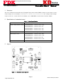
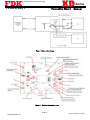
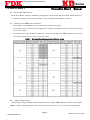
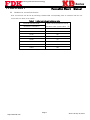
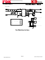
Delivering Next Generation Technology Series FPKD-EVB01 Evaluation Board Manual 1/16 Brick DC-DC Power module KD series (Full digital) Evaluation board user’s manual Version 01.03 Sep 18, 2015 Http://www.fdk.com Delivering Next Generation Technology Series Evaluation Board FPKD-EVB01 Manual 1 Product overview ...................................................................................................................................................................................... 2 2 Specification of evaluation board........................................................................................................................................................ 2 3 Layout ............................................................................................................................................................................................................ 2 4 Terminal, switch description ................................................................................................................................................................. 3 5 Handling method(details of power module, please refer to each KD series data sheet) .............................................. 4 6 5.1 Connection ......................................................................................................................................................................................... 4 5.2 Remote ON/OFF function ........................................................................................................................................................... 6 5.3 Settings of PMBus devise address........................................................................................................................................... 6 5.4 Output voltage setting................................................................................................................................................................... 6 5.5 Over current limited value variable function ........................................................................................................................ 7 Primary function list ................................................................................................................................................................................. 8 Http://www.fdk.com Page 1 Ver 01.03 Sep 18, 2015 Delivering Next Generation Technology Series Evaluation Board FPKD-EVB01 1 Manual Overview This is an evaluation board for KD series (full digital) brick power module. PMBus interface can be used to set the output voltage, turn on/off delay, rise/fall time etc. and also can be used to get the input voltage, output voltage, output current etc. . Control from PC is available, via our USB-PMBus communication interface adapter. 2 Specification of evaluation board Table 1 List of specification Input voltage operation range 36V~60V Output voltage default settings FPKD48*3R330*A evaluation board→3.3V FPKD48*6R018*A evaluation board→6V FPKD48*01208*A evaluation board→12V FPKD48*01806*A evaluation board→18V Output voltage variable range -50%~+20% of default setting Rated output current FPKD48*3R330*A evaluation board→30A FPKD48*6R018*A evaluation board→:16A FPKD48*01208*A evaluation board→8A FPKD48*01806*A evaluation board→5.5A Communication system 3 PMBus Specification Rev.1.2 compliant Layout Figure 1 Http://www.fdk.com Evaluation board top view Page 2 Ver 01.03 Sep 18, 2015 Delivering Next Generation Technology Series Evaluation Board FPKD-EVB01 4 Manual Terminal and switch descriptions Table 2 List of terminal, switch Name Function CN1 Power module input pin (+) CN2 Power module input pin (-) CN3 Remote ON/OFF control pin CN4 Input current measurement-use pin (+) CN5 Input current measurement-use pin (-) CN8 Load connection pin (+) CN9 Load connection pin (-) CN10 For parallel connection PMBus in, out signal pin 1 (PMBus slave connector 1) CN11 PMBus communication pin ※connect to our USB-PMBus communication interface adaptor (PMBus Master connector) CN12 For parallel connection PMBus in, out signal pin 2 (PMBus slave connector 2) TP1 Input voltage measurement-use pin (-) TP2 Input voltage measurement-use pin (+) TP3 Output voltage measurement-use pin (+) TP4 Output voltage measurement-use pin (-) JP1 Short pin for Output voltage (+)- Remote-sense (+) JP2 Short pin for TRIM-UP JP3 Short pin for TRIM-DOWN VR1 TRIM-UP volume adjustment VR2 TRIM-DOWN volume adjustment SW1 Manual remote ON/OFF switch Http://www.fdk.com Page 3 Ver 01.03 Sep 18, 2015 Delivering Next Generation Technology Series Evaluation Board FPKD-EVB01 5 Manual Handling method (details of power module, please refer to each KD series data sheet) 5.1 Connection Connect the power module input pins (CN1, CN2) to DC Power. Connect the load connection pins (CN8, CN9) to the target Load. In order to measure the input current, placed and connect an ammeter within the input current measurement pins (CN4, CN5). (Short these pins CN4,CN5 by a cable if you are not intent to measure the input current) In order to measure the input voltage, please connect the input measurement-use pins (TP1, TP2) to the voltmeter. In order to measure the output voltage, please connect the output measurement-use pins (TP3, TP4) to the voltmeter. Connect the Remote ON/OFF control pin (CN3) if you are intent to Remote ON/OFF outside the evaluation board.(Voltage level of CN3 must be in the range of -0.5V~20V with reference to the CN2) Connect the PMBus interface pin (CN11) to USB-PMBus communication interface adaptor if you are intent to use the communication function to control the evaluation board. (Details of the USB-PMBus communication interface adaptor please refer to USB-PMBus communication interface adaptor user’s manual) Parallel connection of the evaluation boards or connected to other PMBus devises needs parallel connection pin (CN10, CN12) to enable the communications. If the remote sense is unnecessary please short jumper pin (JP1) which short the Output voltage (+) and Remote-sense (+). (open jumper to enable the remote sense, connect Load(+) with the first pin of JP1) Short jumper pin (JP2) to trim-up the output voltage to adjust output voltage higher than the rated output voltage by using TRIM-UP adjustment volume (VR1). Short jumper pin (JP3) to trim-down the output voltage to adjust output voltage lower than the rated output voltage by using TRIM-DOWN adjustment volume (VR2). (Please refer to KD series user’s manual and each KD series Data sheets for further details) Http://www.fdk.com Page 4 Ver 01.03 Sep 18, 2015 Delivering Next Generation Technology Series Evaluation Board FPKD-EVB01 Manual Figure 2 Connection image HIGH LOW Figure 3 Http://www.fdk.com Detailed description view Page 5 Ver 01.03 Sep 18, 2015 Delivering Next Generation Technology Series Evaluation Board FPKD-EVB01 5.2 Manual Remote ON/OFF function The output ON/OFF control is available by changing the manual remote ON/OFF switch (SW1). However, it is under the condition of the remote ON/OFF control pin (CN3) either OPEN or in H level. 5.3 Settings of the PMBus devise address Devise address of the PMBus is sets by mounting the resistances (R1, R2). Corresponding value of resistances and addresses are shown in the Table3. Please use nearest value of E24 series for R1 and R2. The addresses 0 to 8, 12, 40 and 55 in decimal are reserved according to the SMBus specifications and may not be usable. Please do not set those resistance values. Table 3 5.4 Corresponding Addresses and resistance values Output voltage setting Default output voltage settings can be changed either by using the TRIM adjustment volume or by using the PMBus interface command. Please refer to the KD series data sheets or user’s manual for further details. Http://www.fdk.com Page 6 Ver 01.03 Sep 18, 2015 Delivering Next Generation Technology Series Evaluation Board FPKD-EVB01 5.5 Manual Variable over current limit function Over current limit can be set by mounting resistance R3. Corresponding value of resistance and the over current limit are shown in the Table4. Table 4 Limited current and resistance value External resistance(R3) Resistance value(KΩ) Over current protection circuit Operation start current value 10.000 15 15.400 30 23.700 45 36.500 60 54.900 75 84.500 90 130.000 100 OPEN 125 (%) ※(%) is the ratio of rated current value Http://www.fdk.com Page 7 Ver 01.03 Sep 18, 2015 Delivering Next Generation Technology Series Evaluation Board FPKD-EVB01 6 Manual Primary functions list Supported primary functions and their initial configurations, setting/changing method of this product are listed in the table below. Table 5 Function List of functions Default configuration Setting changing method PMBus devise address setting 18(DEC) (12h(HEX)) By attaching resistance Manual remote ON/OFF switch OFF SW1 Remote ON/OFF control Remote ON/OFF pin or Signal through Remote ON/OFF pin PMBus communication or by PMBus command Maximum output voltage control 135% of rated voltage By PMBus command Output voltage trimming 0V By PMBus command Margin voltage setting High: 105% of rated voltage By PMBus command Low: 95% of rated voltage Margin voltage ON/OFF control OFF By PMBus command Turn on delay control 10msec By PMBus command Rise time control 15msec By PMBus command Output over voltage protection 130% of rated voltage By PMBus command Output under voltage protection 40% of rated voltage By PMBus command Output over current protection 125% of rated current By PMBus command Over temperature protection 125℃ By PMBus command Input under voltage protection Start:34.5V By PMBus command Stop:32.5V Input over voltage protection 103V By PMBus command ※Please refer to the KD series data sheet for further details information of available PMBus commands in this product. Http://www.fdk.com Page 8 Ver 01.03 Sep 18, 2015 Delivering Next Generation Technology Series Evaluation Board FPKD-EVB01 Manual Circuit diagram TP2 + C1 100uF 100V C2 33uF 100V 2.2uF C3 100V C4 0T-008 2.2uF 0T-008 VOUT+ 2 0T-008 JP1 8 VINON_OFF VOUT- 4 OCPSEL 5 1 1 4 C5 22uF C6 22uF 25V 25V + 2 SW1 3 7 SENSE+ 100V 3 GND1 CN8 VIN+ 1 CN2 0T-008 TP3 DCDC1 CN5 1 + 0T-008 CN4 10uH C7 22uF JP2 L1 F1 CCF1F5 not-m TP1 CN1 C8 220uF 25V 25V TP4 2 5 2 not-m 6 SDA 11 SDA TRIM 13 SCL SMBALERT/PGOOD 14 ADDR1 ISHARE_O 15 ADDR0 SGND CN9 R3 6 1 VR1 3 500K 0P-008 1 SCL R1 0T-008 GND1 R2 12 SMBALERT 9 ISHARE JP3 G3T-12AP CN3 2 24KΩ 2 10 1 VR2 3 500K 24KΩ GND2 GND2 CN10 1 2 3 4 5 8 TO ANOTHER DCDC MODULE B5B-XH-A 15 1 14 CN11 7 13 DCDC1 PIN NUMBER 2 1 SDA 2 SCL 6 3 12 5 TO USB-I2C BOARD 4 SMBALERT 11 B4B-XH-A 10 3 TOP VIEW 4 9 CN12 ISHARE 1 2 3 4 5 TO ANOTHER DCDC MODULE B5B-XH-A GND2 Figure 4 Evaluation board circuit diagram Http://www.fdk.com Page 9 Ver 01.03 Sep 18, 2015