1
KIT-VR5500-TP
User’s Manual
5. INTERFACE SPECIFICATIONS
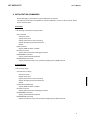
This chapter describes the specifications of the connectors used for control that are required for the
user system.
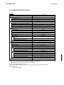
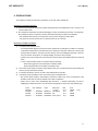
Pin arrangement table
Pin number
Signal name
Input/output (user side)
Treatment (user side)
A1
CLKOUT
Output
22 - 33 Ω series resistor (recommended)
A2
TRCDATA0
Output
22 - 33 Ω series resistor (recommended)
A3
TRCDATA1
Output
22 - 33 Ω series resistor (recommended)
A4
TRCDATA2
Output
22 - 33 Ω series resistor (recommended)
A5
TRCDATA3
Output
22 - 33 Ω series resistor (recommended)
A6
TRCEND
Output
22 - 33 Ω series resistor (recommended)
A7
DDI
Input
4.7k - 10 kΩ pullup
A8
DCK
Input
4.7k - 10 kΩ pullup
A9
DMS
Input
4.7k - 10 kΩ pullup
A10
DDO
Output
A11
DRST-
Input
A12
Rmode*/
Input/Output
22 - 33 Ω series resistor (recommended)
4.7k - 50 kΩ pulldown
4.7k - 10 kΩ pullup
BkTGIO*
A13
NC.
------
Open
Pin number
Signal name
Input/output (user side)
B1-B10
GND
------
Connection to the power GND
B11
NC.
------
Open
B12
NC.
------
Open
B13
+3.3V
------
Connection to the power
Treatment (user side)
A11: Open or It connects ColdReset* via an external circuit with VR5500 ES1.1.
This signal is negative logic.
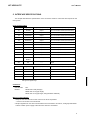
Connectors
Manufacturer:
Models:
KEL
8830E-026-170S (straight)
8830E-026-170L (right angle)
8831E-026-170L (right angle, fixing hardware attached)
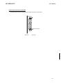
Wiring on Target System
1.Keep the wire from the CPU to the connector as short as possible.
>>100 mm or shorter is recommended.
2.Output signals from CPU are recommended to be connected to connectors, via high-speed CMOS
buffers of which power supply is the same one with CPU I/O buffers.
9