1
FD 1-40 Frequency Downconverter
Instructions and Manual
V 1.1
FD40-Manual_1V1.doc
- Rev C, Nov. 2013 -
Features:
Input Frequency Range 0.1 ... 40MHz
8 Independent Output Channels
Individually Selectable L.O. Frequencies for Every Channel
LabVIEW TM Source Code Available
Typical Application: Ion FT-ICR Experiments
Contents
Safety Hints
.
.
.
Principle of Operation .
.
Target Application
.
.
Internal Structure
.
.
User Interface .
.
.
Useful Gain Settings .
.
How to connect the device
.
Miscellaneous Data
.
.
Frequency Characteristics
.
Appendix A: List of Commands .
.
.
.
.
.
.
.
.
.
.
.
.
.
.
.
.
.
.
.
.
2
3
3
4
5
5
6
7
8
11
Dr. Stefan Stahl - Electronics for Science and Research Kellerweg 23, D - 67582 Mettenheim Germany
www.stahl-electronics.com
2
Safety Hints
This device has to be powered by 230V ac voltage. In normal operation opening of the
device case is not necessary or recommended. If, by any means, opening of the case is
nessessary, observe appropriate safety measures. This device must be operated by
qualified persons only.
The device must not be run under the following conditions:
- Ambient temperature below 0° or above 45°
- relative humidity above 75%
Ventilation: Ensure a clearing distance of at least 5cm around the case (top, rear, and
both sides) to enable air flow cooling. Preventing air flow aroud the device will result in
overheating and irreversible damage.
If by accident the device was mechanically or electrically damaged, consult manufacturer
before putting back into operation or before applying repair measures.
Contact Adress:
Dr. Stefan Stahl - Elektronik-Entwicklung
Kellerweg 23
67582 Mettenheim, Germany
Phone: +49 (0) 6242 2368, mobile: +49 (0) 177-3434 328
.
.
.
.
.
.
.
.
.
.
.
.
.
.
.
.
.
.
.
3
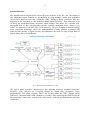
Principle of Operation
This device is intended for downconverion of ion signals from the MHz-range (1 to 40MHz)
down to the LF (low frequency) range of 0…40kHz. It is a multichannel device, which has 2
inputs and 8 output channels. Generally the downconversion acts like illustrated in the
following diagram. This process effectively shifts a selected frequency range down towards
zero, bringing the signals of interest to a more convenient, i.e. smaller frequency range. The
amount of frequency shift is defined by the L.O. (local oscillator) frequency. In the FD 1-40
this frequency can be chosen for every output channel individually. The whole device therefore
provides the possibility to examine 8 independent frequency windows (each 40kHz wide) in
the range from 1MHz to 40MHz, all at the same time and in real time mode (without data loss).
fig. 1: Illustration of a downconversion process. The signal pattern shown is arbitrarily chosen.
Target Application
The envisaged target application is the ion detection via FT-ICR (Fourier-Transform Ion
Cyclotron Resoanance) in a miniaturized EBIT-type Penning ion trap. Unlike conventional FTICR, the cyclotron frequencies are considerably higher, bringing up the neccessity to down
convert all ion signals to lower frequencies. As can be seen in the following illustration, the
down converter forms together with an 8 channel 40kHz-FFT-analyzer a 40MHz FFT analyzer
set up with 8-channel real time capability. Each of the 8 resulting frequency windows
represents a 40kHz wide section of the input signal coming from the ion trap.
fig. 2 : Illustration of the target application, including the 8-channel down converter FD 1-40.
4
Internal Structure
The simplified block diagram below shows the inner structure of the FD 1-40. The signals on
two independent input channels are pre-amplified by programmable variable gain apmplifiers
(VGA-Gain), digitized with fast (100MHz) 12Bit analog-to-digital converters and subsequently down converted by two dedicated digital signal processors. Each processor (type
GC4016) has 4 individual down conversion output channel. This allows for a constant, noninterrupted flow of data, providing the real-time capability mentioned above, which is very
useful, for achieving a real time ion FT-ICR detection. The use of digital (instead of analog)
down conversion technology allows the implementation of many channels in parallel with
relatively little amount of signal circuitry and elliminates the need for using a large bank of
high-Q analog filters for all channels.
fig. 3: Internal structure of the FD 1-40
The typical down converter characteristics, like sideband rejection, stopband supression,
frequency slope (fall-off) are essentially defined by digital filter parameters. These
programmable FIR (finite response filters) are located inside the DDC (Digital Down
Converter) Chips and loaded with a default set of values. After powering the whole device the
microcontroller, which takes control of the whole device, performs this initialization with filter
coefficients.
5
User Interface
The following screen shot, taken from the implemented FD 1-40 setting/control program, gives
an impression of the most important settings. In a user program the functionality is advisable to
integrate in such a way, that only the most important paramters are accessible. Facing the
considerable number of free parameters which could be changed accidentally this procedure is
highly recommended. Source codes in LabVIEWTM are available for easy implementation into
own programs and can ba adapted accordingly.
fig.4 : Screen shot of user interface for controlling the FD 1-40 parameters
Useful Gain Settings
In order to achieve a reasonably good signal to noise ratio (S/N) and avoidance of frequency
crosstalk from unwanted sidebands, the following input settings can be used:
DDC-Gain
VGA Gain
=
=
16, fixed
50 for a signal strength at the input, which is no larger than 1.6mVpp
20 for a signal .
.
.
.
no larger than 4mVpp
10 for a signal .
.
.
.
no larger than 8mVpp
5 for a signal .
.
.
.
no larger than 16mVpp
2 for a signal .
.
.
.
no larger than 40mVpp
1 for a signal .
.
.
.
no larger than 80mVpp
(all voltages are understood at 50Ohm input- and source impedance)
Note, that larger input levels can easily cause fast degradation of stopband-rejection and cause
strong intermodulation effects. In order to run the FD 1-40 in a optimal state, the input signal
has to be monitored, e.g. by an oscilloscope or level meter, and the VGA setting should be
adjusted according to the input level, using the table above.
Note also, that too conservative (= too small) VGA Gain settings will result in poorer
performance of the signal to noise-floor ratio, and should be avoided also. However, the
rejection of unwanted siedebands might be for most FT-ICR application more crucial, therefore
non-linear effects caused by a too large VGA Gain might be of primary interest.
6
For typical sideband rejection figures, see data on page 8-10.
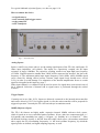
How to connect the device
- to signal sources
- to an external clock/trigger source
- to the control PC
- to FFT analysers
fig. 5
front side view
Analog Inputs:
Inputs A and B (see picture above) are the analog signal inputs of the FD 1-40, and feature 50
Ohms input impedance (AC-related). The inputs are capacitively coupled, the DC-input
resistance is larger 10MOhm. The capacitive coupling results in an input high pass frequency
of 32kHz. Signal frequencies smaller than 32kHz will be supressed the stronger, the lower the
frequency is. The maximum usable input signal frequency is 40.0 MHz. Above 40MHz signal
errors caused by aliasing effects become relevant. Input signal levels should never exceed
2.0Vpp in order to avoid damage. For adaptation of the internal amplification factor to certain
signal levels applied at this input see page 3.
Either input channel A or channel B can be used as source for signal down conversion in any of
the 8 channels. Selection of channel A/B as signal source is performed through the control
software.
Trigger Inputs:
Currently not in use (Okt. 2013). Inputs are directely connected to the internal microcontroller
and can be driven by 0V/5V level pulse signals, in case the microcontroller will be prepared for
triggered operation. Currently the FD 1-40 runs always in continious mode.
10MHz Reference Input:
The FD 1-40 features an highly stable, expensive internal 10MHz reference clock source,
which is based on an oven controlled quartz-oscillator. It has a ultra low temperature drift (<<
0.01ppm/K) and remarkably low aging (< 0.03ppm / yr). Stability in 1s is around 10-11. Since
all internal clocking circuitry is derived from this single clock source, the numbers mentioned
above apply also for all remaining frequencies, i.e. the local oscillator frequency, by which the
signal spectra are shifted, and signal sampling frequency as well.
7
However, if an external clock source is preferred, it is possible to apply a 10MHz
signal to the “10MHz Input” port. In this case, and if the user control is set to “external clock
source“ accordingly, a CMOS-logic level signal of 10MHz can be applied here. The level
should be 0V/3.3V up to 0V/5V signals. No input termination is foreseen. That requires a short
distance to the signal source/signal generator (< 40cm cable length preferable) in order to avoid
signal reflection effects on the transmission line. Input resistance is 650 Ohms nominally. The
external clock frequency should not deviate by more than 1,0% from exact 10MHz (up or
down), otherwise the reliability of communication with a control PC via USB is at risk.
Note, that in case a correct external clock signal is missing, but the device is set to “external
clock” the FD 1-40 will be completely halted without the possibility to switch back to the
internal source. This is caused by the fact, that also the internal microcontroller is supplied
from this single clock source. In this case cycling the supply power will bring him back to
normal operation.
USB-Portand Software Installation
A standard “type A“ connector socket provides the possibility to connect the FD 1-40 to a
control PC. In order to establish communication, the appropriate USB driver has to be installed
on the PC. A Silicon Laboratories CP2102 chip is used for running the USB communication,
so a suitable driver should be used (see provided software, which is included in the delivery)
or downloaded from Silicon Laboratories Inc. The FD 1-40 device will appear and can be
accessed by means of a virtual COM port on the control PC. The functionality of virtual COM
ports is supported by almost all programming languages, including LabVIEWTM. After
installing an appropriate driver, the user software can make use of the established
communcation; send commands and read data.
After this USB connection has been established, install the user surface by extracting the
zipped file “NFsa40.zip” into an appropriate directory and run the “setup” installer.
Down Conversion Outputs
Eight independent low frequency outputs, corresponding to the 8 internal down conversion
channels, are located at the rear side of the device. Their nominal frequency range is 0 to
40kHz, being adapted to the 40kHz range of an OROS FFT analyzer, or similar analyzers, with
which the next signal processing step can be performed. Frequencies above 40kHz should not
be considered for further processing, they contain remains of aliasing sidebands. The nominal
output voltage range is 0..4.6Vpp, having a DC offset around 2.1V. Despite the fact, that the
output impedance is only a few Ohms, and therefore very low, a termination with 50 Ohm is
neither necessary nor recommended in favour of avoiding unneccessary loads on the FD 1-40
outputs.
230V Power
230V ac sine, 50…60Hz mains supply is recommended. Even though the device features a
wide range (110…230V~) switch mode power supply, it is recommended to run the device
with 230V ac. Power consumption is less than 50W.
Miscellaneous Data
Dimensions (W x H x L):
Weight:
254mm x 132mm x 255mm
approx. 4.7 kg
8
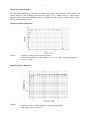
Frequency Characteristics
The following graphs show examples of measured frequency characteristics of the device. Of
special interest is the sideband rejection ratio (pages 9-10), which states, to which degree
signals outside the selected 40kHz window are folded into the region of interest due to nonlinear and quantisation errors.
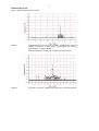
Output Frequency Response
Graph 1:
frequency response of down converted output.
measurement parameters: output channel 1, L.O. 26.517 MHz, input signal at input A
sine wave, 10mVrms
Input Frequency Response
Graph 2:
frequency response of input channels A / B, doubly-logarithmic
input signal: sine wave, 10mVrms
9
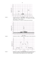
Sideband Rejection
(Note: complex/shifted mode assumed )
Graph 3:
Sideband rejection for L.O at 26.517MHz, 40MHz observation span
settings: VGA Gain = 2, DDC Gain = 16, test signal: sine, 10mVrms
input channel A, output channel 1
mesaurement device: Yokogawa SA2400 spectrum analyzer
Graph 4:
parameters as before, 15MHz observation span, centered around fLO
10
Graph 5:
Sideband rejection for L.O at 20MHz, 40MHz observation span
settings: VGA Gain = 2, DDC Gain = 16, test signal: sine, 10mVrms
input channel A, output channel 1
mesaurement device: Yokogawa SA2400 spectrum analyzer
Graph 6:
Parameters as before, 15 MHz observation span, centered around fLO
Graph 7:
Parameters as before, 500 kHz observation span, centered around fLO
The three central points correspond to the non-suppressed, userselected frequency band and define the level reference (0dB).
11
Appendix A:
List of Commands
Commands of the FD 1-40 / FSA40,
to be sent via the serial USB connection once the latter has been established using Windows™
drivers:
*****************************************************************************
---------> COMMANDS OF FSA40
*****************************************************************************
_____________________________________________________________________________
-> Reset FSA40
----------------------------------------------------------------------------Format: RST[CR] || rst[CR]
This command generate software reset on uC and put system into default state.
Default state means VGA disabled, AD conversion disabled, DDC disabled,
serial output mode configured on DDC, 10Mhz on all chanels are set,
coarse gain for all chanels is set to 2, phase is set to 0 rad,
chanels 1 to 4 input are conigured to bus A,
chanels 5 to 8 input are conigured to bus B.
Response: No
____________________________________________________________________________
-> External/Internal clock
----------------------------------------------------------------------------Format: X[AHex][CR] || x[AHex][CR]
[AHex] - ASCII converted hexadecimal number;
0 means external clock enable,
any other number means internal clock enable.
Response: No
_____________________________________________________________________________
-> VGA enable/disable
----------------------------------------------------------------------------Format: E[Ch][AHex][CR] || e[Ch][AHex][CR]
[Ch] - 'A' or 'B' , selects DDC A or B,
[AHex] - ASCII converted hexadecimal number;
0 means disable,
any other number means enable.
Response: No
_____________________________________________________________________________
-> VGA gain set
----------------------------------------------------------------------------Format: G[Ch][AHex][CR] || g[Ch][AHex][CR]
[Ch] - 'A' or 'B' , selects DDC A or B,
[AHex] - ASCII converted hexadecimal number;
Reguler values are 0 - 7;
Meanings:
0 - Gain 0.5 X,
1 - Gain 1 X,
2 - Gain 2 X,
3 - Gain 5 X,
12
4 - Gain 10 X,
5 - Gain 20 X,
6 - Gain 50 X,
7 - Gain 100 X.
Response: No
_____________________________________________________________________________
-> AD converter enable/disable
----------------------------------------------------------------------------Format: C[Ch][AHex][CR] || c[Ch][AHex][CR]
[Ch] - 'A' or 'B' , selects DDC A or B,
[AHex] - ASCII converted hexadecimal number,
0 means disable,
any other number means enable.
Response: No
_____________________________________________________________________________
-> FIFO write enable
----------------------------------------------------------------------------Format: F[AHex][CR] || f[Ch][AHex][CR]
[AHex] - ASCII converted hexadecimal number;
Meanings:
[bit1][bit0] - 01 - write enable bus A FIFO and send
first block of data,
02 - write enable bus B FIFO and send
first block of data,
03 - write enable both buses FIFOs and
send first block of data,
[bit3][bit2] - Block data size
00 - 256 points
01 - 512 points
10 - 1024 points
11 - 2048 points
Response: Yes
Format of response: V{[Hex] X n}[CR] || W{[Hex] X n}[CR]
V means A bus, W means B bus;
Hex - hexadecimal number 0 - ff;
n = Block data size X 2 bytes
Point (2 bytes) is organised as: [LSB][MSB].
!!! FIFO's deep is 32768 words (16 bits).
FIFO's write will be automaticaly disabled after full flag would be set.
_____________________________________________________________________________
-> FIFO A block read
----------------------------------------------------------------------------Format: V[CR] || v[CR]
Response: Yes
Format of response: V{[Hex] X n}[CR]
V means A bus;
Hex - hexadecimal number 0 - ff;
n = Block data size X 2 bytes
Point (2 bytes) is organised as: [LSB][MSB].
!!! FIFO's deep is 32768 words (16 bits).
FIFO's write will be automaticaly disabled after full flag would be set.
_____________________________________________________________________________
13
-> FIFO B block read
----------------------------------------------------------------------------Format: W[CR] || w[CR]
Response: Yes
Format of response: W{[Hex] X n}[CR]
W means B bus;
Hex - hexadecimal number 0 - ff;
n = Block data size X 2 bytes
Point (2 bytes) is organised as: [LSB][MSB].
!!! FIFO's deep is 32768 words (16 bits).
FIFO's write will be automaticaly disabled after full flag would be set.
_____________________________________________________________________________
-> DDC register read
----------------------------------------------------------------------------Format: D[Ch][R][AHex1][AHex2][AHex3][AHex4][CR] ||
d[Ch][r][AHex1][AHex2][AHex3][AHex4][CR]
[Ch] - 'A' or 'B' , selects DDC A or B,
[AHex1,2,3,4] - ASCII converted hexadecimal number;
[AHex1][AHex2] - Page number;
Regular pages:
Global page 0,
Cfir pages:
Ch1 0,1, Ch2 8,9, Ch3 16,17, Ch4 24,25,
Pfir pages:
Ch1 2-5 Ch2 10-13, Ch3 18-21, Ch4 26-29,
Freq page:
Ch1 6, Ch2 14, Ch3 22, Ch4 30,
Control page:
Ch1 7, Ch2 15, Ch3 23, Ch4 31,
Resampler pages: 32-65,
Output data pages: 96, 97,
Output config page: 98.
[AHex3][AHex4] - Byte address;
Regular values:
Global page: 0-7,
Cfir pages 1, 9, 17, 25: 16-21,
Freq pages 6, 14, 22, 30: 16-21,
Output config page 98: 16-28,
All other pages: 16-31.
Response: Yes
Format of response: D[Ch][R][AHex1][AHex2][AHex3][AHex4][AHex5][AHex6][CR]
[Ch] - 'A' or 'B' , selects DDC A or B,
[AHex1,2,3,4,5,6] - ASCII converted hexadecimal number;
[AHex1][AHex2] - Page number;
Regular pages:
Global page 0,
Cfir pages:
Ch1 0,1, Ch2 8,9, Ch3 16,17, Ch4 24,25,
Pfir pages:
Ch1 2-5 Ch2 10-13, Ch3 18-21, Ch4 26-29,
Freq page:
Ch1 6, Ch2 14, Ch3 22, Ch4 30,
Control page:
Ch1 7, Ch2 15, Ch3 23, Ch4 31,
Resampler pages: 32-65,
Output data pages: 96, 97,
Output config page: 98.
[AHex3][AHex4] - Byte address;
Regular values:
14
Global page: 0-7,
Cfir pages 1, 9, 17, 25: 16-21,
Freq pages 6, 14, 22, 30: 16-21,
Output config page 98: 16-28,
All other pages: 16-31.
[AHex5][AHex6] - Value of register 0 - ff.
_____________________________________________________________________________
-> DDC register write
----------------------------------------------------------------------------Format: D[Ch][W][AHex1][AHex2][AHex3][AHex4][AHex5][AHex6][CR]
[Ch] - 'A' or 'B' , selects DDC A or B,
[AHex1,2,3,4,5,6] - ASCII converted hexadecimal number;
[AHex1][AHex2] - Page number;
Regular pages:
Global page 0,
Cfir pages:
Ch1 0,1, Ch2 8,9, Ch3 16,17, Ch4 24,25,
Pfir pages:
Ch1 2-5 Ch2 10-13, Ch3 18-21, Ch4 26-29,
Freq page:
Ch1 6, Ch2 14, Ch3 22, Ch4 30,
Control page:
Ch1 7, Ch2 15, Ch3 23, Ch4 31,
Resampler pages: 32-65,
Output data pages: 96, 97,
Output config page: 98.
[AHex3][AHex4] - Byte address;
Regular values:
Global page: 0-7,
Cfir pages 1, 9, 17, 25: 16-21,
Freq pages 6, 14, 22, 30: 16-21,
Output config page 98: 16-28,
All other pages: 16-31.
[AHex5][AHex6] - Value of register 0 - ff.
Response: No
______________________________________________________________________________
-> DDC configuration command
----------------------------------------------------------------------------Format: D[Ch]C[AHex][CR] || d[Ch]c[AHex][CR]
[Ch] - 'A' or 'B' , selects DDC A or B,
[AHex] - ASCII converted hexadecimal number;
[bit1][bit0] - 00 - means config DDC to complex mode
with uC output;
01 - means config DDC to real mode with
serial output;
20 - means config DDC to complex mode with
serial output;
[bit6][bit5] - this bits impacts real mode with serial
output, only;
00 - output filters 68%,
01 - output filters 80% (default value),
20 - output filters 100%.
Response: No
_____________________________________________________________________________
-> DDC output FIFO read
----------------------------------------------------------------------------Format: A[AHex][CR] || a[AHex][CR]
[AHex] - ASCII converted hexadecimal number;
Meanings:
15
[bit3][bit2][bit1][bit0]
bit0 = 1 - Chanel A
bit1 = 1 & bit0 = 0 - Chanel B
[bit3][bit2] - Block data size
00 - 256 points
01 - 512 points
10 - 1024 points
11 - 2048 points
Response: Yes
Format of response: A{[Hex] X n}[CR] || B{[Hex] X n}[CR]
A or B chanel;
Hex - hexadecimal number 0 - ff;
n = Block data size X 8 X 2 bytes;
Point (8 X 2 bytes) is organised as:
AI([LSB][MSB]), AQ([LSB][MSB]),
BI([LSB][MSB]), BQ([LSB][MSB]),
CI([LSB][MSB]), CQ([LSB][MSB]),
DI([LSB][MSB]), DQ([LSB][MSB]).
!!! This command is aplicable if DDC is configured in uC complex mode, only.
_____________________________________________________________________________
-> DDC chanel synch
----------------------------------------------------------------------------Format: Y[AHex][CR]
[AHex] - ASCII converted hexadecimal number;
Meanings:
1 - synchronise processes in DDC A,
2 - synchronise processes in DDC B,
3 - synchronise processes in both DDCs (!!!Important - this
command have to be send after turning on or reconfiguration
both DDC for proper operation!!!).
Response: No
_____________________________________________________________________________
-> System state
----------------------------------------------------------------------------Format: S?[CR]
Response: Yes
Format of response: SS[AHex1][AHex2][CR]
[AHex1,2] - ASCII converted hexadecimal number;
[AHex1] - [bit0] - 0 means external clock,
1 means internal clock,
[bit1] - 0 means no errors detected,
1 means errors detected,
[bit2] - 0 output mode of chanel A is serial,
1 output mode of chanel A is uC,
[bit3] - 0 output mode of chanel B is serial,
1 output mode of chanel B is uC,
[bit4] - 0 means VGA of chanel A disabled,
1 means VGA of chanel A enabled,
[bit5] - 0 means VGA of chanel B disabled,
1 means VGA of chanel B enabled,
[bit6] - 0 means AD conversion of A chanel is disabled,
1 means AD conversion of A chanel is enabled,
[bit7] - 0 means AD conversion of B chanel is disabled,
1 means AD conversion of B chanel is enabled;
[AHex2] - [bit0] - 0 means external clock,
1 means internal clock,
[bit1] - 0 means no errors detected,
1 means errors detected,
[bit2] - 0 output mode of chanel A is serial,
16
[bit3]
[bit4]
[bit5]
[bit6]
[bit7]
1 output mode of
chanel A is uC,
- 0 output mode of chanel B is serial,
1 output mode of chanel B is uC,
- 0 means VGA of chanel A disabled,
1 means VGA of chanel A enabled,
- 0 means VGA of chanel B disabled,
1 means VGA of chanel B enabled,
- 0 means AD conversion of A chanel is disabled,
1 means AD conversion of A chanel is enabled,
- 0 means AD conversion of B chanel is disabled,
1 means AD conversion of B chanel is enabled;
***************************************************************************************
***************************************************************************************
***************************************EXAMPLES****************************************
***************************************************************************************
***************************************************************************************
//...Regular start-up procedure
EA1
GA1
CA1
EB1
GB1
CB1
Y3
//...Enable VGA A
//...Set gain of VGA A to 1
//...Enable AD conversion A
//...Enable VGA B
//...Set gain of VGA B to 1
//...Enable AD conversion A
//...Synchronise DDCs
//...Frequency setting
DAW0612f8
DAW061314
DAW061400
DAW061520
//...Ch1 set to 10000100.00 Hz
DAW0E12f1
DAW0E1329
DAW0E1400
DAW0E1520
//...Ch2 set to 10000200.00 Hz
DAW1612ea
DAW16133e
DAW161400
DAW161520
//...Ch3 set to 10000300.00 Hz
DAW1E12e2
DAW1E1353
DAW1E1400
DAW1E1520
//...Ch4 set to 10000400.00 Hz
DBW0612db
DBW061368
DBW061400
DBW061520
//...Ch5 set to 10000500.00 Hz
DBW0E12d4
DBW0E137d
DBW0E1400
DBW0E1520
//...Ch6 set to 10000600.00 Hz
DBW1612cc
DBW161392
DBW161400
DBW161520
//...Ch7 set to 10000700.00 Hz
DBW1E12c5
DBW1E13a7
DBW1E1400
DBW1E1520
//...Ch4 set to 10000800.00 Hz
// fn = 2^32 * f / 80 000 000.00Hz (32 bit number, positive values only)
17
//...Bus selecting
DAW071b01
DAW0F1b01
DAW171b01
DAW1F1b01
DBW071b00
DBW0F1b00
DBW171b00
DBW1F1b00
//...Ch1 input
//...Ch2 input
//...Ch3 input
//...Ch4 input
//...Ch5 input
//...Ch6 input
//...Ch7 input
//...Ch8 input
from
from
from
from
from
from
from
from
bus B
bus B
bus B
bus B
bus A
bus A
bus A
bus A
//...Coarse gain setting
DAW071900
DAW0F1910
DAW171920
DAW1F1930
DBW071940
DBW0F1950
DBW171960
DBW1F1970
//...Ch1 coarse gain set to 1
//...Ch2 coarse gain set to 2
//...Ch3 coarse gain set to 4
//...Ch4 coarse gain set to 8
//...Ch5 coarse gain set to 16
//...Ch6 coarse gain set to 32
//...Ch7 coarse gain set to 64
//...Ch8 coarse gain set to 128
//...Coniguring output filter in real mode, serial output
DAC01 //...68% filter select on DDC A outputs
DBC01 //...68% filter select on DDC B outputs
Y3
//...Synchronise DDCs
//...Default configuration
DAC21 //...80% filter select on DDC A outputs
DBC21 //...80% filter select on DDC B outputs
Y3
//...Synchronise DDCs
DAC41 //...100% filter select on DDC A outputs
DBC41 //...100% filter select on DDC B outputs
Y3
//...Synchronise DDCs