1
LogiCORE IP
Interleaver/De-Interleaver v6.0
DS250 March 1, 2011
Product Specification
Introduction
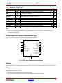
LogiCORE IP Facts Table
The interleaver/de-interleaver core is appropriate for any
application that requires data to be rearranged in an interleaved fashion, including many popular communications
standards such as CDMA2000 and DVB Terrestrial(T),
Cable(C), and Satellite(S).
The multiple configuration mode is particularly useful for
standards that require swapping between a number of
convolutional interleavers, for example, ITU J.83 Annex B.
Core Specifics
Supported
Device Family (1)
Virtex-7 and Kintex-7,
Virtex-6, Virtex-5, Virtex-4,
Spartan-6, Spartan-3/XA, Spartan-3E/XA,
Spartan-3A/3AN/3A DSP/XA
Supported User
Interfaces
Not Applicable
Provided with Core
Documentation
Features
Design Files
•
Example Design
•
•
High-speed compact
symbol interleaver/de-interleaver
Supports many popular standards, such as DVB and
CDMA2000
Drop-in module for Kintex™-7, Virtex ®-7,
Spartan®-6, Virtex-6, Virtex-5, Virtex-4, and
•
•
•
•
•
•
•
•
Forney Convolutional and Rectangular Block type
architectures available
Easy-to-use interface signals
Fully synchronous design using a single clock
Symbol size from 1 to 256 bits
Internal or external symbol RAM
Convolutional type features:
• Parameterizable number of branches
• Parameterizable branch lengths
• Supports uniform and non-uniform branch
length increments
• Multiple configurations with on-the-fly
swapping
Rectangular Block type features:
• Parameterizable, variable, or selectable numbers
of rows and columns
• Parameterizable or variable block size
• Can change numbers of rows/columns or block
size at start of each new block
• Row and column permutations
• Multiple permutations for selectable rows or
columns
• Input validity checking
Use with Xilinx CORE Generator™ software and
Xilinx System Generator for DSP v13.1
Available under terms of the SignOnce IP Site License
Netlist
Not Provided
Test Bench
VHDL
Constraints File
Simulation
Model
Spartan-3/XA, Spartan-3E/XA and Spartan-3A/AN/3A
DSP/XA FPGAs
•
Product Specification
Not Applicable
VHDL behavioral model in the xilinxcorelib library
VHDL UniSim structural model
Verilog UniSim structural model
Tested Design Tools
Design Entry
Tools
Simulation
CORE Generator tool 13.1
System Generator for DSP 13.1
Mentor Graphics ModelSim 6.6d
Cadence Incisive Enterprise Simulator (IES) 10.2
Synopsys VCS and VCS MX 2010.06
ISIM 13.1
Synthesis Tools
N/A
Support
Provided by Xilinx, Inc.
1. For a complete listing of supported devices, see the release notes
for this core.
© Copyright 2003 - 2006, 2008, 2010 - 2011 Xilinx, Inc. XILINX, the Xilinx logo, Kintex, Virtex, Spartan, ISE and other designated brands included herein are
trademarks of Xilinx in the United States and other countries. Simulink is a registered trademark of The MathWorks, Inc. All other trademarks are the property of their
respective owners.
DS250 March 1, 2011
Product Specification
www.xilinx.com
1
LogiCORE IP Interleaver/De-Interleaver v6.0
Functional Description
An interleaver is a device that rearranges the order of a sequence of input symbols. The term symbol is used to
describe a collection of bits. In some applications, a symbol is a single bit. In others, a symbol is a bus.
The classic use of interleaving is to randomize the location of errors introduced in signal transmission. Interleaving
spreads a burst of errors out so that error correction circuits have a better chance of correcting the data.
If a particular interleaver is used at the transmit end of a channel, the inverse of that interleaver must be used at the
receive end to recover the original data. The inverse interleaver is referred to as a de-interleaver.
Two types of interleaver/de-interleavers can be generated with this core: Forney Convolutional and Rectangular
Block. Although they both perform the general interleaving function of rearranging symbols, the way in which the
symbols are rearranged and their methods of operation are entirely different.
For very large interleavers, it may be preferable to store the data symbols in external memory. The core provides an
option to store data symbols in internal FPGA RAM or in external RAM. This is explained in more detail in the section External Symbol Memory, page 30.
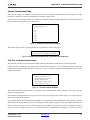
Forney Convolutional Operation
Figure 1 shows the operation of a Forney Convolutional Interleaver. The core operates as a series of delay line shift
registers. Input symbols are presented to the input commutator arm on DIN. Output symbols are extracted from the
output commutator arm on DOUT. Both commutator arms start at branch 0 and advance to the next branch after the
next rising clock edge. After the last branch (B-1) has been reached, the commutator arms both rotate back to branch
0 and the process is repeated.
X-Ref Target - Figure 1
0
1
2
L
2*L
DOUT
DIN
(B-3)
(B-2)
(B-1)
(B-3) * L
(B-2) * L
(B-1) * L
Figure 1: Forney Convolutional Interleaver
In Figure 1, the branches increase in length by a uniform amount, L. The core allows interleavers to be specified in
this way, or the branch lengths can be passed in via a file, allowing each branch to be any length. Although branch
0 appears to be a zero-delay connection, there is still a delay of a number of clock cycles between DIN and DOUT
because of the fundamental latency of the core. For clarity, this is not illustrated in Figure 1.
DS250 March 1, 2011
Product Specification
www.xilinx.com
2
LogiCORE IP Interleaver/De-Interleaver v6.0
The only difference between an interleaver and a de-interleaver is that branch 0 is the longest in the de-interleaver
and the branch length is decremented by L rather than incremented. Branch (B-1) has length 0. This is illustrated in
Figure 2.
If a file is used to specify the branch lengths, it is arbitrary whether the resulting core is called an interleaver or
de-interleaver. All that matters is that one must be the inverse of the other. If a file is used, each branch length is
individually controllable. This is illustrated in Figure 3. The file syntax is shown in Figure 13, page 25.
X-Ref Target - Figure 2
0
(B-1) * L
1
(B-2) * L
2
(B-3) * L
DOUT
DIN
(B-3)
(B-2)
2*L
L
(B-1)
Figure 2: Forney Convolutional De-interleaver
X-Ref Target - Figure 3
0
1
2
branch_length_vector(0)
branch_length_vector(1)
branch_length_vector(2)
DOUT
DIN
(B-3)
(B-2)
(B-1)
branch_length_vector(B-3)
branch_length_vector(B-2)
branch_length_vector(B-1)
Figure 3: Forney Convolutional Interleaver/De-interleaver with Branch Lengths Set by File
DS250 March 1, 2011
Product Specification
www.xilinx.com
3
LogiCORE IP Interleaver/De-Interleaver v6.0
Configuration Swapping
It is possible for the core to store a number of pre-defined configurations. Each configuration can have a different
number of branches and branch length constant. It is even possible for each configuration to have every individual
branch length defined by file.
The configuration can be changed at any time by asserting FD and NEW_CONFIG and selecting the required configuration on CONFIG_SEL.
The core assumes all configurations are either for an interleaver or de-interleaver, depending on what was selected
in the GUI. It is possible to switch between interleaving and de-interleaving by defining the individual branch
lengths for every branch of each configuration.
The details for each configuration are specified in a COE file. See COE Files for Multiple Configurations, page 25 for
details. The timing for a configuration swap is described in the section Multiple Configuration Timing, page 28.
Rectangular Block Operation
The Rectangular Block Interleaver works by writing the input data symbols into a rectangular memory array in a
certain order and then reading them out in a different, mixed-up order. The input symbols must be grouped into
blocks. Unlike the Convolutional Interleaver, where symbols can be continuously input, the Rectangular Block
Interleaver inputs one block of symbols and then outputs that same block with the symbols rearranged. No new
inputs can be accepted while the interleaved symbols from the previous block are being output.
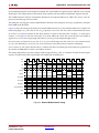
The rectangular memory array is composed of a number of rows and columns as shown in Figure 4.
X-Ref Target - Figure 4
Row\Column
0
1
...
(C-2)
(C-1)
0
1
:
(R-2)
(R-1)
Figure 4: Row and Column Indexing Scheme
The Rectangular Block Interleaver operates as follows:
1.
All the input symbols in an entire block are written row-wise, left to right, starting with the top row.
2.
Inter-row permutations are performed if required.
3.
Inter-column permutations are performed if required.
4.
The entire block is read column-wise, top to bottom, starting with the left column.
The de-interleaver operates in the reverse way:
1.
All the input symbols in an entire block are written column-wise, top to bottom, starting with the left column.
2.
Inter-row permutations are performed if required.
3.
Inter-column permutations are performed if required.
4.
The entire block is read row-wise, left to right, starting with the top row.
DS250 March 1, 2011
Product Specification
www.xilinx.com
4
LogiCORE IP Interleaver/De-Interleaver v6.0
An example of Rectangular Block Interleaver operation is shown in Figure 5. This example has 3 rows, 4 columns
and a block size of 12. The inter-row permutation pattern is {2, 0, 1}. This means row 0 is permuted to row 2, row 1
is permuted to row 0, and row 2 is permuted to row 1. The meaning of the permute vector differs for the de-interleaver.
X-Ref Target - Figure 5
Input Data = {0, 1, 2, 3, 4, 5, 6, 7, 8, 9, 10, 11}
Write row-wise, starting with top row
0
1
2
3
4
5
6
7
8
9
10
11
Inter-row permutations Pr[0:2] = {2, 0, 1}
4
5
6
7
8
9
10
11
0
1
2
3
Output Data = {4, 8, 0, 5, 9, 1, 6, 10, 2, 7, 11, 3}
Figure 5: Block Interleaving Example with Row Permutations
Although this example shows only row permutations, it is possible to do both row and column permutations simultaneously. This is shown in Figure 6.
Figure 7 shows the output data from the interleaver of Figure 6 being de-interleaved. All the parameters are the
same, apart from mode, which is set to de-interleaver in this case. Notice how the permute vectors are identical to
those for the interleaver, but they are interpreted in a different way. This ensures that output data from the interleaver is correctly restored to the original data by the de-interleaver, as shown in Figure 8.
The inter-row permutation pattern is again {2, 0, 1}. However, for the de-interleaver this means row 2 is permuted
to row 0, row 0 is permuted to row 1, and row 1 is permuted to row 2.
DS250 March 1, 2011
Product Specification
www.xilinx.com
5
LogiCORE IP Interleaver/De-Interleaver v6.0
X-Ref Target - Figure 6
Input Data = {0, 1, 2, 3, 4, 5, 6, 7, 8, 9, 10, 11}
Write row-wise, starting with top row
0
1
2
3
4
5
6
7
8
9
10
11
Inter-row permutations Pr[0:2] = {2, 0, 1}
4
5
6
7
8
9
10
11
0
1
2
3
Inter-column permutations Pc[0:3] = {3, 1, 0, 2}
6
5
7
4
10
9
11
8
2
1
3
0
Output Data = {6, 10, 2, 5, 9, 1, 7, 11, 3, 4, 8, 0}
Figure 6: Block Interleaving Example with Row and Column Permutations
The core can be configured with fixed, variable, or selectable rows and columns. The block size can be fixed, variable or set to always equal R * C. If the block size is variable or less than R * C, row and column permutations are not
supported. If the block size is less than R * C, the interleaver is described as pruned.
DS250 March 1, 2011
Product Specification
www.xilinx.com
6
LogiCORE IP Interleaver/De-Interleaver v6.0
X-Ref Target - Figure 7
Input Data = {6, 10, 2, 5, 9, 1, 7, 11, 3, 4, 8, 0}
Write column-wise, starting with left column
6
5
7
4
10
9
11
8
2
1
3
0
Inter-row permutations Pr[0:2] = {2, 0, 1}
2
1
3
0
6
5
7
4
10
9
11
8
Inter-column permutations Pc[0:3] = {3, 1, 0, 2}
0
1
2
3
4
5
6
7
8
9
10
11
Output Data = {0, 1, 2, 3, 4, 5, 6, 7, 8, 9, 10, 11}
Figure 7: Block De-interleaving Example with Row and Column Permutations
Row permutations are not supported if the row type is variable. Column permutations are not supported if the column type is variable.
Selectable rows/columns can be used when the number of possible values for the number of rows or columns is
known and is relatively small. In this mode, the number of rows/columns is still run-time variable but chosen from
a small set of predetermined values, stored within the core. Permutations are possible when using selectable rows
or columns. A different permutation vector can be stored for each row or column select value.
DS250 March 1, 2011
Product Specification
www.xilinx.com
7
LogiCORE IP Interleaver/De-Interleaver v6.0
X-Ref Target - Figure 8
Input Data = {0, 1, 2, 3, 4, 5, 6, 7, 8, 9, 10, 11}
Interleaver, I
Transmit
{6, 10, 2, 5, 9, 1, 7, 11, 3, 4, 8, 0}
De-interleaver, I-1
(All parameters identical to
Interleaver, except for Mode.)
Output Data = {0, 1, 2, 3, 4, 5, 6, 7, 8, 9, 10, 11}
Figure 8: Block Interleaver, De-interleaver Operation
In general, the most efficient core is one with constant rows, columns, and block size. The number of optional pins
should be kept to a minimum. For every optional pin or extra feature, such as row or column permutations, there is
a price to pay in terms of area and speed.
More details on the available block size types and choosing the appropriate one are given in the section Block Size
Type, page 21.
The core also provides optional outputs to check the validity of inputs, such as BLOCK_SIZE. These can sometimes
be useful in a receiver to detect if things have gone catastrophically wrong before further error correction is
attempted.
Block Interleaver Specifications
Sometimes, a specification requires a Rectangular Block Interleaver, but it is specified in the form of an equation. It
is not always immediately obvious that the equation represents a block interleaver.
It may be necessary to evaluate the equation for a number of values to see if it can be translated into the parameters
required by the block interleaver core.
For example, one way of defining a block interleaver is to specify that the symbols are all written to a memory in
sequential order (0, 1, ... block_size-1) as in the write phase of Figure 5. The symbols are then read back from memory in an order defined by the following equation:
Read Addressi = 2c(i mod R) + BROc(Round Down(i/R))
where i increments from 0 to block_size-1, 2c is the number of columns and R is the number of rows. BROc(x) is the
bit-reversed c-bit value of x, for example, BRO3(1) = 4.
DS250 March 1, 2011
Product Specification
www.xilinx.com
8
LogiCORE IP Interleaver/De-Interleaver v6.0
Examination of the Read Address equation shows that the first part, 2c(i mod R), yields the start address of each
row. The second part, BROc(Round Down(i/R)), yields how far along the row to go. The BRO part produces column
permutations. For example, if c=3, column 4 is permuted to column 1 and column 1 is permuted to column 4.
If c=3 and R=4, then the resultant column permute vector is {0, 4, 2, 6, 1, 5, 3, 7}.
Pinout
Some of the pins are optional. These should be selected only if they are genuinely required, as their inclusion might
result in an increase in the core size.
Representative symbols for the Forney Convolutional type and Rectangular Block type are shown in Figure 9 and
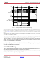
Figure 11, respectively.
Table 1 summarizes the signal functions. They are described in more detail in the remainder of this section. Timing
examples are shown in the section Timing, Latency and FDO Delay, page 27.
Table 1: Core Signal Pinout
SIgnal
BLOCK_SIZE<>
Direction
Input
Description
Conv
Rect
Block Size: If block size is variable.
-
O
BLOCK_SIZE_VALID
Output
Block Size Valid: Indicates if an invalid value is sampled on
BLOCK_SIZE.
-
O
BLOCK_START
Output
Block Start: Indicates first symbol of block on DOUT.
-
O
BLOCK_END
Output
Block End: Indicates last symbol of block on DOUT.
-
O
CLK
Input
Clock: Clock input, all core operation is synchronous with the CLK input.
M
M
CE
Input
Clock Enable: Freezes state of core when low.
O
O
COL<>
Input
Number of Columns: If the number of columns is variable, this specifies
how many columns are in the block.
-
O
COL_SEL<>
Input
Column Select: If the number of columns is selectable, this specifies
which predefined value for the number for columns to use.
-
O
COL_SEL_VALID
Output
Column Select Valid: A 1 means “valid.” A 0 means “invalid.”
-
O
COL_VALID
Output
Column Valid: A 1 means “valid.” A 0 means “invalid.”
-
O
CONFIG_SEL<>
Input
Configuration Select: Select one from a number of pre-defined
configurations.
O
-
DIN<>
Input
Data Input: Input symbols to be interleaved/deinterleaved.
M
M
Data Output: Output symbols after interleaving/deinterleaving.
M
M
First Data: Indicates first symbol on DIN.
M
M
First Data Out: Flags propagation of first symbol to DOUT.
O
-
Input
New Data: Indicates new data on DIN.
M
O
Output
New Data Out: ND delayed by latency.
O
-
New Configuration: Indicates that configuration has changed.
O
-
Read Address: For external symbol RAM.
O
O
Read Data: Read data value from external symbol RAM.
O
O
DOUT<>
FD
FDO
ND
NDO
NEW_CONFIG
Output
Input
Output
Input
RD_ADDR<>
Output
RD_DATA<>
Input
RD_EN
Output
Read Enable: High when reading data from external symbol RAM.
O
O
RDY
Output
Output Ready: Indicates valid data on port DOUT.
O
O
RFD
Output
Ready for Data: Indicates that the core is ready to receive new data.
O
O
DS250 March 1, 2011
Product Specification
www.xilinx.com
9
LogiCORE IP Interleaver/De-Interleaver v6.0
Table 1: Core Signal Pinout (Cont’d)
SIgnal
RFFD
Direction
Output
Description
Conv
Rect
Ready for First Data: Indicates that FD can be asserted.
O
O
ROW<>
Input
Number of Rows: If the number of rows is variable, this specifies how
many rows are in the block.
-
O
ROW_SEL<>
Input
Row Select: If the number of rows is selectable, this specifies which
predefined value for the number for rows to use.
-
O
ROW_SEL_VALID
Output
Row Select Valid: A 1 means “valid.” A 0 means “invalid.”
-
O
ROW_VALID
Output
Row Valid: 1 means “valid.” A 0 means “invalid.”
-
O
Synchronous Reset: Reinitializes core control logic.
O
O
SCLR
Input
WR_ADDR<>
Output
Write Address: For external symbol RAM.
O
O
WR_DATA<>
Output
Write Data: Write data value for external symbol RAM.
O
O
WR_EN
Output
Write Enable: High when writing data to external symbol RAM.
O
O
Notes:
1.
2.
<> signifies that a signal can be a multi-bit bus.
The last two columns define whether the pin is Mandatory (M), Optional (O) or not available, (-) for the Convolutional and
Rectangular Block Interleavers.
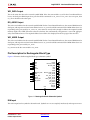
Pin Description for Forney Convolutional Type
Figure 9 illustrates the Forney Convolutional type schematic symbol.
X-Ref Target - Figure 9
DIN
FD
ND
CE
SCLR
CONFIG_SEL
NEW_CONFIG
RD_DATA
CLK
DOUT
FDO
NDO
RDY
RFD
RFFD
WR_DATA
WR_ADDR
RD_ADDR
WR_EN
RD_EN
Figure 9: Forney Convolutional Schematic Symbol
DIN Input
This is the input bus for symbols to be interleaved. Symbols on DIN are sampled, interleaved, and output on DOUT.
FD Input
The FD (First Data) input is used to:
1.
Initialize the core commutator arms to the branch 0 tap.
2.
Indicate that the value on the DIN port is the first symbol in a sequence of symbols.
DS250 March 1, 2011
Product Specification
www.xilinx.com
10
LogiCORE IP Interleaver/De-Interleaver v6.0
The term “valid FD pulse” is used to describe the case when FD and ND (and CE, if appropriate) are asserted
logic-high while a rising edge of CLK occurs. It is recommended that a valid FD pulse last for only a single clock
cycle. However, the core supports the case where it is asserted logic-high for multiple clock cycles. The data symbols, sampled from the DIN port, all pass through branch 0 while valid FD pulses are sampled.
Only one valid FD pulse is required after power-on-reset or initialization. FD can be asserted subsequently. However, the behavior then depends on the value on the optional RFFD output (or its internal equivalent if there is no
RFFD output).
Referring to Figure 1, the commutator arms cycle periodically, returning to the initial starting position after B symbols have been sampled. A logic-high on the RFFD output indicates that the symbol sampled on the DIN port
(assuming a valid ND pulse is also sampled), passes through the branch 0 tap of the input commutator arm. Therefore, sampling a valid FD pulse while RFFD is logic-high does not actually affect the synchronization of the commutator arms (assuming that a valid FD pulse has been previously sampled). This is the preferred mode of operation,
as it ensures that symbols already in the branch memory eventually appear on the DOUT port in the appropriate
interleaved/de-interleaved order.
If a valid FD pulse is received when RFFD is logic-low, the core aborts the previous interleave operation and the
commutator arms are reset to branch 0. The periodic cycling of the commutator arms is disrupted. Therefore, the
symbols that are already in the branch memory do not appear on the DOUT output port in the expected interleaved/de-interleaved order.
ND Input
When the ND (New Data) input is sampled logic-high, it signals the core that a new symbol on DIN should be sampled on the same rising clock edge. Every new input symbol, including the first, must be qualified by ND. ND differs
from CE in that the core is not frozen when ND is low. The core processes the new sample as far as possible. Like all
the synchronous inputs, ND is ignored if CE is low. For every input symbol qualified by ND, a new symbol is also output on DOUT.
CE Input
The Clock Enable input is an optional input pin. When CE is deasserted (low), all the synchronous inputs are
ignored and the core remains in its current state.
An example of CE operation is shown in Figure 10. In this case, the core ignores symbol Di2 and all the other synchronous inputs at this time. The state of the core is frozen while CE is low.
SCLR Input
When SCLR is asserted (high), all the core flip-flops are synchronously initialized. The core remains in this state
until SCLR is deasserted.
The synchronous initialization has the effect of resetting the commutator arms to the branch 0 position. The
branches themselves are not cleared.
SCLR is an optional pin, as the core can function correctly without it. The mandatory FD input causes the logic to be
synchronously initialized every time it is asserted.
DS250 March 1, 2011
Product Specification
www.xilinx.com
11
LogiCORE IP Interleaver/De-Interleaver v6.0
X-Ref Target - Figure 10
CLK
SCLR
CE
DIN
Di0
Di1
Di2
Di3
DOUT
Figure 10: CE and SCLR Timing
CONFIG_SEL Input
If the number of configurations is more than one, then CONFIG_SEL selects which configuration to use for the current block. CONFIG_SEL is sampled when FD is asserted. NEW_CONFIG must also be asserted. More details on the
use of multiple configurations are given in the section Configuration Swapping, page 4.
NEW_CONFIG Input
NEW_CONFIG must be asserted at the same time as FD when a configuration swap is to occur. This distinguishes
between an ordinary FD pulse and one where the configuration is also to be swapped. NEW_CONFIG must always be
asserted for the very first FD pulse. This causes the core to load the initial configuration. The core cannot operate
correctly until a valid FD pulse with NEW_CONFIG high has occurred at least once.
DOUT Output
This is the output bus for the interleaved/de-interleaved symbols. This bus always has the same width as DIN. One
new symbol is output on DOUT for each input symbol sampled on DIN. The number of clock cycles between an
input symbol being sampled and a new output appearing on DOUT is termed the latency of the core. Note that this
is not the number of cycles from a particular symbol being sampled on DIN and the same symbol finally appearing
on DOUT. For the first symbol, this is termed the FDO delay and is dependent on the interleaver branch lengths. This
delay is different for each input symbol because of the interleaving process. The latency is always the same, regardless of branch lengths. Latency and the FDO delay are described further on, in the section Timing, Latency and FDO
Delay, page 27.
FDO Output
First Data Out (FDO) is a time-delayed version of the FD input. FDO is asserted high when the value sampled on DIN
at the time of the FD pulse appears on DOUT. The FDO delay is dependent on the latency and the branch lengths. The
FDO output is useful for synchronizing circuits downstream of the interleaver. It can be used to tell those circuits
when to start a new block if the data is arranged in blocks.
NDO Output
New Data Out (NDO) is a time-delayed version of the ND input. A new symbol is output on DOUT for every symbol
input on DIN. NDO is asserted high whenever a new symbol is output. The delay from ND to NDO is dependent only
on the latency, as the symbol being qualified by NDO is not the same as the one qualified by ND. The NDO output is
also useful for synchronizing circuits downstream of the interleaver. It can be used to tell those circuits when to
sample a new input.
NDO remains low until after the first valid FD pulse.
DS250 March 1, 2011
Product Specification
www.xilinx.com
12
LogiCORE IP Interleaver/De-Interleaver v6.0
RDY Output
The RDY (Ready) output is similar to NDO. It signals valid data on DOUT. The difference from NDO is that RDY is not
asserted until the input symbol sampled with the first FD pulse finally appears on DOUT. NDO is asserted as each zero
(or other symbol) that was in the branch memory prior to the FD pulse is flushed out. RDY is not asserted for this
data.
If branch 0 has length 0, RDY and NDO are identical. This is because the first symbol output on DOUT after the FD
pulse is the one that was sampled with FD.
RFD Output
Ready for Data (RFD) indicates that the core is ready to sample new data on DIN. For the Convolutional type, RFD
is permanently high because the core is always ready for new data. The output is provided only for consistency
with other Xilinx cores that provide handshaking signals. The core does not sample new data during synchronous
resets, even though RFD is high.
RFFD Output
When Ready for First Data (RFFD) is asserted high, it indicates that FD may be asserted without affecting the synchronization of the commutator arms. When a valid FD pulse is received, RFFD is deasserted immediately. It then
remains low until B symbols have been sampled. B is the number of branches, as shown in Figure 1. It is then reasserted high, indicating that the commutator arms are back at position 0. An FD pulse can safely be applied at this
time, although it is unnecessary unless an FDO output pulse is required.
Although RFFD is an optional output, it is always required internal to the core because FD-aborts must be detected.
An FD-abort takes place when a valid FD pulse occurs when the commutator arms are not located at branch 0. This
situation is described in the FD Input section.
Unlike all the other outputs, RFFD is not a glitch-free output.
RD_EN Output
This optional pin is present when external symbol memory is selected. It is the read enable for the RAM. The core
asserts the RD_EN output high when there is a valid read address on RD_ADDR and it needs to read the contents of
that RAM location.
WR_EN Output
This is the write enable for the external symbol RAM. The core asserts the WR_EN output high when there is a valid
write address on WR_ADDR and it needs to write to that RAM location.
RD_DATA Input
This is the read data bus from the external symbol RAM. It has the same width as DIN. For the Convolutional Interleaver, one of the dual-port RAM output data ports should be connected to RD_DATA. This should be a different
port from the one used by WR_DATA.
RD_DATA is simply passed straight back out on DOUT. It is not registered or modified in any way inside the core.
DS250 March 1, 2011
Product Specification
www.xilinx.com
13
LogiCORE IP Interleaver/De-Interleaver v6.0
WR_DATA Output
This is the write data bus to the external symbol RAM. It has the same width as DIN. For the Convolutional Interleaver, the dual-port RAM input data port should be connected to WR_DATA. If RD_DATA uses one port, then
WR_DATA should use the other port.
RD_ADDR Output
This is the read address for the external symbol RAM. For the Convolutional Interleaver, the external RAM must be
dual-port, with separate read and write address busses. RD_ADDR should be connected to the RAM address bus corresponding to the port used by RD_DATA. RD_ADDR must be exactly wide enough to address the required symbol
memory depth. The CORE Generator software calculates this automatically and generates a core with appropriately sized address busses. The required address bus width is also displayed on the last page of the core GUI.
WR_ADDR Output
This is the read address for the external symbol RAM. For the Convolutional Interleaver, the external RAM must be
dual-port, with separate read and write address busses. WR_ADDR should be connected to the RAM address bus corresponding to the port used by WR_DATA.
WR_ADDR must be the same width as RD_ADDR.
Pin Description for Rectangular Block Type
Figure 11 illustrates the Rectangular Block type schematic symbol.
X-Ref Target - Figure 11
DIN
FD
ND
CE
SCLR
BLOCK_SIZE
COL
COL_SEL
ROW
ROW_SEL
RD_DATA
DOUT
BLOCK_START
BLOCK_END
RDY
RFD
RFFD
BLOCK_SIZE_VALID
COL_VALID
COL_SEL_VALID
ROW_VALID
ROW_SEL_VALID
WR_DATA
WR_ADDR
RD_ADDR
WR_EN
CLK
RD_EN
Figure 11: Rectangular Block Schematic Symbol
DIN Input
This is the input bus for symbols to be interleaved. Symbols on DIN are sampled, interleaved, and output on DOUT.
DS250 March 1, 2011
Product Specification
www.xilinx.com
14
LogiCORE IP Interleaver/De-Interleaver v6.0
FD Input
The First Data (FD) input is used to indicate that the value on the DIN port is the first symbol in a new block.
The term “valid FD pulse” is used to describe the case when FD (and ND and CE, if appropriate) is asserted
logic-high while a rising edge of CLK occurs.
FD must be asserted at the beginning of each new block input to the core. FD should not be reasserted until the core
is ready to accept a new block of data. This is N sample periods (while data is sampled) plus N clock periods (while
data is output), where N equals the block size. The optional RFFD output is provided to determine when it is safe to
start a new block.
If a valid FD pulse is received before the core is ready for a new block to be started, the core aborts the previous
interleave operation and starts a new block. The internal operation of the core is disrupted, which means the symbols that are already in the symbol memory do not appear on the DOUT output port in the expected interleaved/de-interleaved order. DOUT is undefined until data from the new block starts to appears on DOUT. The
optional RFFD output is available when it is necessary to determine when it is safe to assert FD.
ND Input
When the optional ND (New Data) input is sampled logic-high, it signals the core that a new symbol on DIN should
be sampled on the same rising clock edge. If ND is selected, every new input symbol, including the first, must be
qualified by ND. ND differs from CE in that the core is not frozen when ND is low. The core processes the new sample
as far as possible. Like all the synchronous inputs, ND is ignored if CE is low. ND is also ignored when the core is busy
processing a received block. The optional RFD output is available to flag when this is the case, if required.
CE Input
The Clock Enable input is an optional input pin. When CE is deasserted (low), all the synchronous inputs are
ignored and the core remains in its current state.
An example of CE operation is shown in Figure 10. In this case, the core ignores symbol Di2 and all the other synchronous inputs at this time. The state of the core is frozen while CE is low.
BLOCK_SIZE Input
This optional input is automatically selected if variable block sizes are chosen in the GUI. The width of the input is
also entered in the GUI. Take care not to make this port any wider than necessary, as this increases the size of the
core.
BLOCK_SIZE is resampled at the start of each new block when FD is sampled high. Illegal values on BLOCK_SIZE
can be detected using the BLOCK_SIZE_VALID output, if necessary. See Block Size Type, page 21, for details of illegal BLOCK_SIZE values.
COL Input
This optional input is automatically selected if the variable number of columns option is chosen in the GUI. The
width of the input is also entered in the GUI. As with BLOCK_SIZE, care should be taken not to make this port any
wider than necessary, as this increases the size of the core.
COL is resampled at the start of each new block when FD is sampled high. The number sampled from the COL input
tells the core how many columns there are in the block. Illegal values on COL can be detected using the COL_VALID
output, if necessary.
DS250 March 1, 2011
Product Specification
www.xilinx.com
15
LogiCORE IP Interleaver/De-Interleaver v6.0
COL_SEL Input
This optional input is automatically selected if the selectable number of columns option is chosen in the GUI. The
width of the input is determined from the number of selectable columns entered in the GUI. Again, care should be
taken not to make this any larger than necessary, as this increases the size of the core.
COL_SEL is resampled at the start of each new block when FD is sampled high. The number sampled from the
COL_SEL input tells the core which value to use from the COE file. 0 means use the first value, 1 the second, and so
on.
The value sampled on COL_SEL must correspond to a predefined number of columns in the COE file. An illegal
value on COL_SEL can be detected using the COL_SEL_VALID output, if necessary.
An example of an illegal COL_SEL value would be three possible numbers of columns being defined in the COE file.
These would be selected using a two-bit COL_SEL bus. ‘00,’ ‘01’ and ‘10’ would all be valid COL_SEL inputs, but ‘11’
would be illegal because there is no corresponding column number for that COL_SEL value in the COE file.
ROW Input
This optional input is automatically selected if the variable number of rows option is chosen in the GUI. The width
of the input is also entered in the GUI. Care should be taken not to make this port any wider than necessary, as
doing so increases the size of the core.
ROW is resampled at the start of each new block when FD is sampled high. The number sampled from the ROW input
tells the core how many rows are in the block. Illegal values on ROW can be detected using the ROW_VALID output,
if necessary.
ROW_SEL Input
This optional input is automatically selected if the selectable number of rows option is chosen in the GUI. The width
of the input is determined from the number of selectable rows entered in the GUI. Care should be taken not to make
this any larger than necessary, as doing so increases the size of the core.
ROW_SEL is resampled at the start of each new block when FD is sampled high. The number sampled from the
ROW_SEL input tells the core which value to use from the COE file. 0 means use the first value, 1 the second, and so
on. An illegal value on ROW_SEL can be detected using the ROW_SEL_VALID output, if necessary. Illegal ROW_SEL
values are defined in the same way as for COL_SEL. See the description of COL_SEL Input for more details.
SCLR Input
When SCLR is asserted (high), all the core flip-flops are synchronously initialized. The core remains in this state
until SCLR is deasserted.
The synchronous initialization resets only the core control logic. The symbol memory itself is not cleared.
SCLR is an optional pin; the core can function correctly without it. The mandatory FD input causes the control logic
to be synchronously initialized every time it is asserted.
DOUT Output
This is the output bus for the interleaved/de-interleaved symbols. This bus always has the same width as DIN.
The core does not start to output the symbols from the block in an interleaved/de-interleaved fashion until all the
symbols from the block have been sampled.
DS250 March 1, 2011
Product Specification
www.xilinx.com
16
LogiCORE IP Interleaver/De-Interleaver v6.0
The number of clock cycles between the last input symbol in a block being sampled and the first symbol from that
block appearing on DOUT is termed the latency of the core. Note that this definition differs from the one used for the
Convolutional interleaver. The number of cycles from the first symbol being sampled on DIN to the first symbol of
the same block finally appearing on DOUT is termed the FDO delay or BLOCK_START delay. This delay is dependent
on the interleaver block size.
The delay from an input symbol being sampled on DIN to that same symbol finally appearing on DOUT is different
for each input symbol because of the interleaving process.
Latency and the BLOCK_START delay are described further on in Timing, Latency and FDO Delay, page 27.
BLOCK_START Output
BLOCK_START has similar functionality to FDO in the Convolutional interleaver. It is asserted high when the first
symbol of a block appears on DOUT. The BLOCK_START delay is dependent on the latency and the block size. The
BLOCK_START output is useful for synchronizing circuits downstream of the interleaver. It can be used to tell those
circuits when to start a new block.
BLOCK_END Output
BLOCK_END is asserted high when the last symbol of a block appears on DOUT. As with BLOCK_START, this cannot
be the last symbol from the block as sampled on DIN, because of the interleaving process.
BLOCK_SIZE_VALID Output
This optional output is available when the block size is not constant, that is, if the block size type is either variable
or equal to R * C.
If the block size type is variable, BLOCK_SIZE_VALID signals whether a legal or illegal value is sampled on the
BLOCK_SIZE input. If an illegal value is sampled, BLOCK_SIZE_VALID goes low a predefined number of clock
cycles later.
If the block size type is R * C, BLOCK_SIZE_VALID signals that the block size, generated from the values sampled
on ROW or ROW_SEL, or on COL or COL_SEL, is legal.
Table 2 lists the number of clock cycles from FD being sampled high to BLOCK_SIZE_VALID (or any of the other
*_VALID outputs) changing. Once a *_VALID output has gone low, it remains low until “Valid Delay” clock cycles
after the next block is started. The latency is defined in Table 5 and always equals a constant. Thus, the Valid Delay
is always constant.
Table 2: Clock Cycles from FD
Block Size
Type
Selectable Rows
or Columns
Valid Delay
(clock cycles)
Variable
-
latency-2
Row x Column
No
2
Row x Column
Yes
4
Regardless of the block size type chosen, the block size must never go below the absolute minimum value given in
Table 3.
DS250 March 1, 2011
Product Specification
www.xilinx.com
17
LogiCORE IP Interleaver/De-Interleaver v6.0
COL_VALID Output
This optional output is available when a variable number of columns is selected. If an illegal value is sampled on the
COL input, COL_VALID goes low a predefined number of clock cycles later. Table 2 lists the number of clock cycles
from FD being sampled high to COL_VALID changing.
See Table 3 for details of illegal COL values.
COL_SEL_VALID Output
This optional output is available when a selectable number of columns is chosen. If an illegal value is sampled on
the COL_SEL input, COL_SEL_VALID goes low a predefined number of clock cycles later. Table 2 lists the number
of clock cycles from FD being sampled high to COL_SEL_VALID changing.
See COL_SEL Input for an explanation of an illegal COL_SEL value.
ROW_VALID Output
This optional output is available when a variable number of rows is selected. If an illegal value is sampled on the
ROW input, ROW_VALID goes low a predefined number of clock cycles later. Table 2 lists the number of clock cycles
from FD being sampled high to ROW_VALID changing.
See Table 3 for details of illegal ROW values.
ROW_SEL_VALID Output
This optional output is available when a selectable number of rows is chosen. If an illegal value is sampled on the
ROW_SEL input, ROW_SEL_VALID goes low a predefined number of clock cycles later. Table 2 lists the number of
clock cycles from FD being sampled high to ROW_SEL_VALID changing.
See ROW_SEL Input for an explanation of an illegal ROW_SEL value.
RDY Output
The RDY (Ready) output signals valid interleaved/de-interleaved data on DOUT. Under normal operation, RDY is
high the whole time a block is being output on DOUT.
RFD Output
RFD (Ready for Data) indicates that the core is ready to sample new data on DIN. Under normal operation, RFD is
high. If N is the block size, the core samples N symbols and RFD immediately goes low. RFD remains low for N clock
cycles and then go high again.
ND and DIN are ignored when RFD is low.
If any of the *_VALID outputs go low, RFD (and RFFD) are forced high one clock cycle later.
RFFD Output
When RFFD (Ready for First Data) is asserted high, it indicates that FD can be safely asserted without affecting any
processing for previous blocks.
When a valid FD pulse is received, RFFD is deasserted immediately. It then remains low until N symbols have been
sampled and a further N clock cycles have elapsed, where N is the block size. It is then reasserted high, indicating
that an FD pulse can be safely applied at this time.
DS250 March 1, 2011
Product Specification
www.xilinx.com
18
LogiCORE IP Interleaver/De-Interleaver v6.0
If any of the *_VALID outputs go low, RFFD (and RFD) are forced high one clock cycle later.
RD_EN Output
This optional pin is present when external symbol memory is selected. The Rectangular Block Interleaver uses only
a single port symbol RAM and RD_EN is simply driven high all the time. Note that it is high even when CE is low,
so care must be taken if using it to drive an enable input external to the core. It might be necessary to AND it with
CE.
WR_EN Output
This is the write enable for the external symbol RAM. This has the same functionality as described previously for
the Convolutional Interleaver.
RD_DATA Input
This is the read data bus from the external symbol RAM. It has the same functionality as described previously for
the Convolutional Interleaver, except the RAM only needs to be single-port in this case.
WR_DATA Output
This is the write data bus to the external symbol RAM. It has the same functionality as described previously for the
Convolutional Interleaver, except the RAM only needs to be single-port in this case.
RD_ADDR Output
This is the address for the external symbol RAM. As the RAM is only single-port for the Rectangular Block Interleaver, there only needs to be one address bus. RD_ADDR and WR_ADDR are actually identical for the Rectangular
Block Interleaver.
WR_ADDR Output
For the Rectangular Block Interleaver, this is just a duplicate of RD_ADDR.
CORE Generator Software Parameters
The CORE Generator GUI for the Interleaver/De-interleaver core uses several screens for setting core parameters.
To move between screens, click Next or Back. After selecting the desired parameters for type of core you want, click
Generate to generate the core when you reach the final screen.
Note that some parameters are relevant to both types of interleavers, and some are specific to only one type.
Component Name
Used as the base name of the output files generated for the core. Names must begin with a letter and must be composed of the following characters: a to z, 0 to 9 and “_”.
Memory Style
The following options are available:
•
Distributed. The core should not use any block memories, if possible. This is useful if they are required
elsewhere in the design.
DS250 March 1, 2011
Product Specification
www.xilinx.com
19
LogiCORE IP Interleaver/De-Interleaver v6.0
•
Block. The core should use block memories wherever possible. This keeps the number of slices used to a
minimum, but may waste block memory.
•
Automatic. Allow the core to use the most appropriate style of memory for each case, based on required
memory depth.
Symbol Memory Type
Allows the symbol memory to be specified as internal or external. If external is selected, then all the optional pins
required for external memory access are automatically added.
Mode
Determines whether the core is to be an interleaver or de-interleaver.
For the Forney Convolutional type, the branch lengths are incremented from branch 0, as shown in Figure 1, or decremented from branch 0, as shown in Figure 2. If the branch lengths are specified in a file, the mode is irrelevant.
For the Rectangular Block type, this determines whether a write rows, read columns or write columns, read rows
operation is performed.
Symbol Width
This is the bus width of the DIN and DOUT ports.
Pipelining
Three levels of pipelining are available. Select Maximum if speed is important. This might result in a slight increase
in area. The latency of the Convolutional type also increases slightly. The behavior of the Rectangular Block type is
identical whether level of pipelining is selected.
In general, it is recommended that Maximum pipelining is used.
Medium and Maximum pipelining have the effect of adding input registers to DIN, FD, and ND in the Convolutional type. Maximum pipelining results in some additional internal registering within the core compared to
Medium pipelining.
In the Rectangular Block type, a number of internal circuits are pipelined to improve performance. Medium and
Maximum pipelining are actually identical for the Rectangular Block type. It might be possible to further improve
performance by adding extra registers on all the synchronous inputs and outputs external to the core.
Optional Pins
Check the boxes of the optional pins that are required. Each selected pin can result in more FPGA resources being
used and can result in a reduced maximum operating frequency.
System Generator for DSP Graphical User Interface
The Symbol Interleaver/De-interleaver core is available through Xilinx System Generator for DSP, a design tool that
enables the use of the model-based design environment Simulink® for FPGA design. The Symbol Interleaver/De-interleave core is one of the DSP building blocks provided in the Xilinx blockset for Simulink. The core
can be found in the Xilinx Blockset in the Communication section. The block is called “Interleaver/De-interleaver
6.0." See the System Generator User Manual for more information.
DS250 March 1, 2011
Product Specification
www.xilinx.com
20
LogiCORE IP Interleaver/De-Interleaver v6.0
The controls in the System Generator GUI work identically to those in the CORE Generator GUI, although the layout has changed slightly. See "CORE Generator Software Parameters," page 19, for detailed information about all
other parameters.
Forney Convolutional Specific Parameters
Number of Branches
The value for the variable B in Figure 1, Figure 2, and Figure 3. The value must always be specified, even when
using a file to define branch lengths.
Length of Branches
Either a constant difference between branch lengths, as in Figure 1 and Figure 2, or the branch lengths specified
from a file, as in Figure 3. Figure 13 provides an example of the file syntax in the latter case.
Number of Configurations
If greater than 1, the core is generated with CONFIG_SEL and NEW_CONFIG inputs. The parameters for each configuration are defined in a COE file. The number of parameters defined must exactly match the number of configurations specified.
Architecture
Controls whether look-up table ROMs or logic circuits are used to compute some of the internal results in the core.
Which option is best depends on the other core parameters. It is recommended that both options are tried. This
parameter has no effect on the core behavior.
Rectangular Block-Specific Parameters
Block Size Type
There are three possibilities:
1.
Constant. Block size never changes. The block can be pruned (block size < row * col). The block size must be
chosen so that the last symbol is on the last row. An unpruned interleaver uses a smaller quantity of FPGA
resources than a pruned one, so pruning should be used only if necessary.
Figure 12 provides an example with three rows and four columns. Using the preceding rule, the only legal block
sizes are 9, 10, 11 and 12.
This block size type can be used only if the row and column types are also set to constant.
Row and column permutations are not supported for pruned block sizes.
2.
Rows * Columns. If the number of rows and columns is constant, selecting this option has the same effect as
setting the block size type to constant and entering a value of rows * columns for the block size.
If the number of rows or columns is not constant, selecting this option means the core calculates the block size
automatically whenever a new row or column value is sampled. Pruning is impossible with this block size type.
3.
Variable. Block size is sampled from the BLOCK_SIZE input at the beginning of every block. The value
sampled on BLOCK_SIZE must be such that the last symbol falls on the last row, as previously described.
If the block size is already available external to the core, selecting this option is usually more efficient than
selecting “rows * columns” for the block size type.
DS250 March 1, 2011
Product Specification
www.xilinx.com
21
LogiCORE IP Interleaver/De-Interleaver v6.0
Row and column permutations are not supported for the variable block size type.
X-Ref Target - Figure 12
0
1
2
3
4
5
6
7
8
9
X
X
Block Size = 10 - Legal
0
1
2
3
4
5
6
X
X
X
X
X
Block Size = 7 - Illegal
Figure 12: Legal and Illegal Block Sizes
Block Size Constant Value
This parameter is relevant only if constant block size type is selected. It must meet the constraints described in the
Block Size Type section.
BLOCK_SIZE Port Width
This parameter is relevant only if variable block size type is selected. It sets the width of the BLOCK_SIZE input bus.
The smallest possible value should be used to keep the core as small as possible.
Column Type
There are three possibilities:
1.
Constant. The number of columns is always equal to the Column Constant Value parameter.
2.
Variable. The number of columns is sampled from the COL input at the start of each new block. Column
permutations are not supported for the variable column type.
3.
Selectable. COL_SEL is sampled at the start of each new block. This value is then used to select from one of the
possible values for number of columns provided in the COE file.
Column Constant Value
This parameter is relevant only if constant column type is selected. The number of columns is fixed at this value.
COL Port Width
This parameter is relevant only if variable column type is selected. It sets the width of the COL input bus. The smallest possible value should be used to keep the core as small as possible.
Minimum Number of Columns
This parameter is relevant only if variable column type is selected. In this case, the core has to cope potentially with
a wide range of possible values for the number of columns. If the smallest value that will actually occur is known,
then the amount of logic in the core can sometimes be reduced. The largest possible value should be used for this
parameter to keep the core as small as possible.
DS250 March 1, 2011
Product Specification
www.xilinx.com
22
LogiCORE IP Interleaver/De-Interleaver v6.0
Number of Selectable Columns
If the selectable column type has been chosen, this parameter defines how many valid selection values have been
defined in the COE file. Only add select values you need.
Use Column Permute File
This tells the CORE Generator software that a column permute vector exists in the COE file and column permutations are to be performed. Remember this is only possible for unpruned interleaver/de-interleavers.
Row Type
There are three possibilities:
1.
Constant. The number of rows is always equal to the Row Constant Value parameter.
2.
Variable. The number of rows is sampled from the ROW input at the start of each new block. Row permutations
are not supported for the variable row type.
3.
Selectable. ROW_SEL is sampled at the start of each new block. This value is then used to select from one of the
possible values for number of rows provided in the COE file.
Row Constant Value
This parameter is relevant only if constant row type is selected. The number of rows is fixed at this value.
ROW Port Width
This parameter is relevant only if variable row type is selected. It sets the width of the ROW input bus. The smallest
possible value should be used to keep the core as small as possible.
Number of Selectable Rows
If the selectable row type has been chosen, this parameter defines how many valid selection values have been
defined in the COE file. Only add select values you need.
Minimum Number of Rows
This parameter is relevant only if variable row type is selected. In this case the core has to potentially cope with a
wide range of possible values for the number of rows. If the smallest value that will actually occur is known, then
the amount of logic in the core can sometimes be reduced. The largest possible value should be used for this parameter to keep the core as small as possible.
Use Row Permute File
This tells the CORE Generator software that a row permute vector exists in the COE file, and row permutations are
to be performed. Remember this is possible only for unpruned interleaver/de-interleavers.
DS250 March 1, 2011
Product Specification
www.xilinx.com
23
LogiCORE IP Interleaver/De-Interleaver v6.0
Parameter Ranges
Valid ranges for the parameters are provided in Table 3.
Table 3: Parameter Ranges
Parameter
Min
Max
Notes
1
256
-
Number of Configurations
1
256
Number of Branches
2
256
1
Branch Length Constant
1
See notes
1,2
Branch Lengths
1
See notes
1
Block Size Constant
6
65025
1,3
Block Size Width
3
16
1
Column Constant
2
255
1,4
Column Width
2
8
1
Minimum Number of Columns
2
255
1,4
Number of Selectable Columns
2
32
-
Row Constant
1
255
1,4
Row Width
1
8
1
Minimum Number of Rows
1
255
1,4
Number of Selectable Rows
2
32
-
Symbol Width
Forney Convolutional:
Rectangular Block:
Notes:
1.
2.
3.
4.
This parameter is limited such that the maximum depth of individual memories within the core do not exceed certain limits. The GUI
detects if these limits have been exceeded. This can mean the maximum value allowed by the GUI appears to be less than the
absolute maximum value given in Table 3. In reality, these parameters are limited by the maximum size of device available.
The branch length constant is the value entered as the constant difference between consecutive branches. The GUI displays the
range of legal values, based on the restrictions mentioned in Note 1.
Block Size Constant must be within the following range: (R-1) * C < Block Size Constant <= R * C, where R = number of rows and
C = number of columns. If there is only a single row, then Block Size Constant must equal the number of columns.
The resulting block size must be within the absolute limits for Block SIze Constant given in this table.
COE File Format
In certain cases, some parameter values are passed to the CORE Generator software via a COE (COEfficient) file.
This is an ASCII text file with a single radix header followed by a number of vectors. The radix can be 2, 10, or 16.
Each vector must be terminated by a semi-colon.
The GUI reads the COE file and writes out one or more MIF files when the core is generated. The VHDL and Verilog
behavioral simulation models for the core rely on these MIF files. For correct operation when using MIF files, they
must be copied to the directory in which the simulation is to be run.
The vectors used in the COE file differ depending on whether the core is a Forney Convolutional or Rectangular
Block type.
DS250 March 1, 2011
Product Specification
www.xilinx.com
24
LogiCORE IP Interleaver/De-Interleaver v6.0
Forney Convolutional Type
If the branch lengths are defined in a file, then it must be a correctly formatted COE file. The length of all the
branches is defined in a comma-separated list in a branch_length_vector.
Figure 13 shows an example COE file for a Forney Convolution interleaver with eight branches. Note that the number of branches must also be set to 8 in the GUI.
X-Ref Target - Figure 13
radix=10;
branch_length_vector=
3,
10,
20,
40,
80,
160,
320,
640;
Figure 13: Example Convolutional COE File
The branch length values can also be placed on a single line as shown in Figure 14.
X-Ref Target - Figure 14
radix=10;
branch_length_vector=3,10,20,40,80,160,320,640;
Figure 14: Example Convolutional COE File Values on a Single Line
COE Files for Multiple Configurations
The COE file is used to specify the branch length constant and number of branches for each configuration.
Figure 15 shows a COE file for an example with 16 configurations. If CONFIG_SEL = 0 then the interleaver has 128
branches and a branch length constant of 1. If CONFIG_SEL = 3 then the interleaver has 64 branches and a branch
length constant of 2.
X-Ref Target - Figure 15
radix=10;
number_of_branches_vector=
128,128,128,64,128,32,128,16,128,
8,128,128,128,128,128,128;
branch_length_constant_vector=
1,1,2,2,3,4,4,8,5,16,6,1,7,1,8,1;
Figure 15: ITU J.83 Annex B COE File
The number of elements in the number_of_branches_vector and the branch_length_constant_vector must equal the
number of configurations.
If the number of configurations is not a power of two, then out-of-range values on the CONFIG_SEL input results in
the core selecting configuration 0.
It is possible to define the individual branch length for every branch in each configuration. If this option is selected,
then the branch_length_constant_vector must be replaced with a branch_length_vector. The number of elements in
this vector must be the exact sum of all the elements of the number_of_branches_vector. An example is shown in
Figure 16. In this example, if CONFIG_SEL = 0, then an interleaver with branches of lengths 1, 2, 3, and 4 is selected.
DS250 March 1, 2011
Product Specification
www.xilinx.com
25
LogiCORE IP Interleaver/De-Interleaver v6.0
If CONFIG_SEL = 1, an interleaver with branches of 4, 3, 2, and 1 is selected. This is one way of having a single core
switch between interleaving and de-interleaving. If CONFIG_SEL = 2, an interleaver with branches of 1, 4 and 5 is
selected.
X-Ref Target - Figure 16
radix=10;
number_of_branches_vector=
4,4,3;
branch_length_vector=
1,2,3,4,4,3,2,1,1,4,5;
Figure 16: Multiple Configuration COE File Defining Each Individual Branch Length
Rectangular Block Type
If row or column permutations are to be used, then the row and/or column permutation vectors are passed to the
CORE generator software using a COE file. Figure 17 shows an example COE file for the permutations used in
Figure 6.
X-Ref Target - Figure 17
radix=10;
row_permute_vector=
2,0,1;
col_permute_vector=
3,1,0,2;
Figure 17: Example Rectangular COE File
If the row or column type is “selectable,” the row and/or column select vectors are also passed in via the COE file.
These tell the core how to map the value sampled on the ROW_SEL and COL_SEL inputs to a particular number of
rows or columns. If row or column permutations are to be used in conjunction with selectable rows or columns,
then it is possible to have a different permute vector for every row and column select value. For example, in
Figure 18 there are three selectable row values. If ROW_SEL = ‘00’ the interleaver has three rows. ‘01’ gives four rows
and ‘10’ gives five rows. ‘11’ is an illegal ROW_SEL input because a fourth value is not defined in the
row_select_vector. Also, if ROW_SEL=’00’ the row permute vector is [2, 0, 1]. If ROW_SEL=’01’ the vector is [3, 2, 0, 1],
and if ROW_SEL=’10’ the vector is [0, 1, 2, 3, 4] (that is, no row permutations). The col_select_vector and col_permute
vector work in the same way.
The supplied COE file must be compatible with the other parameters entered in the GUI, such as number of selectable rows.
X-Ref Target - Figure 18
radix=10;
row_select_vector=
3,4,5;
col_select_vector=
4,6,5;
row_permute_vector=
2,0,1,
3,2,0,1,
0,1,2,3,4;
col_permute_vector=
3,1,0,2,
3,1,0,2,4,5,
2,1,3,0,4;
Figure 18: Example Rectangular COE File with Selectable Rows and Columns
DS250 March 1, 2011
Product Specification
www.xilinx.com
26
LogiCORE IP Interleaver/De-Interleaver v6.0
Timing, Latency and FDO Delay
The precise definitions of latency and FDO Delay differ for the different types of interleaver/de-interleaver. Each is
described separately.
Forney Convolutional Timing
The latency is the number of clock cycles from a new symbol being sampled on DIN, to a new symbol appearing on
DOUT. Note that these are generally not the same symbol, as they have been interleaved or de-interleaved.
The latency is dependent on the pipelining level selected as shown in Table 4.
Table 4: Forney Convolutional Latency
Pipelining
Latency(1)
Minimum
3
Medium
4
Maximum
5
Note:
1.
Add one clock cycle to these figures if external symbol RAM is used.
The FDO delay is the delay from the first symbol being sampled with an FD pulse to that symbol being output on
DOUT. The FDO delay is comprised of two parts: a number of valid ND pulses, including the FD pulse, and the
latency. The GUI reports the FDO delay as the number of new symbols that must be sampled, including the FD pulse,
plus latency clock cycles. This is when FDO is actually asserted, assuming CE is high all the time. The number of new
symbols that must be sampled is dependent on the number of branches and the length of branch 0.
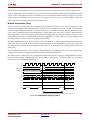
An example, with a latency of four clock cycles, is shown in Figure 19. In this example, the input symbols Di2 and
Di7 are ignored because ND is low. When Di0 is sampled, a new symbol, Do0, appears on DOUT after four clock
cycles. Di0 finally appears on DOUT when FDO goes high. Therefore, Do4 = Di0. Do5 is not the same as Di1 because
the input symbols have been interleaved. Do1 and Do5 are held for two clock cycles because Di2 and Di7 are not
sampled due to ND.
X-Ref Target - Figure 19
CLK
FD
ND
DIN
Di0
Di1
Di2
DOUT
Di3
Di4
Di5
Do0
Di6
Do1
Di7
Di8
Do2
Di9
Do3
Di10
Do4
Di11
Do5
FDO
NDO
RDY
RFFD
FDO Delay = 5 samples + Latency of 4 clock cycles
Latency = 4
Figure 19: Forney Convolutional Interleaver Interface Timing
The FDO delay is reported as five samples (Di0 to Di5, Di2 not included) plus the four clock cycle latency. Note that
ND being low does affect the count of the number of samples, but it does not affect the latency.
DS250 March 1, 2011
Product Specification
www.xilinx.com
27
LogiCORE IP Interleaver/De-Interleaver v6.0
This is the first FD pulse after a reset, so RDY stays low until FDO is asserted. NDO is just a delayed version of ND.
In this example, there are four branches. RFFD goes low after the first sample is taken and goes high after the fourth
sample is taken. This indicates that the commutator arms are connected to branch 0 again. See Figure 3. It is now
safe to reassert FD, although this is not necessary. RFFD goes low again as soon as another sample is taken and
remains low until the commutator arms are back at branch 0.
Multiple Configuration Timing
Figure 20 shows the timing when the configuration is swapped using CONFIG_SEL. In this example, the core
switches from configuration 0 to configuration 1 at time t1. RFFD was high when FD was asserted, so the core continues to output configuration 0 data for Latency clock cycles, as defined previously. After this number of clock
cycles, DOUT is unknown until the first configuration 1 symbol appears on DOUT. This is at time t2. After this point
only configuration 1 data can be output, as the interleaver configuration has now been switched. The “XX” in the
figure indicates that DOUT is undefined between valid configuration 1 output symbols. It actually outputs some
residual value left over from a previous configuration interleaver.
Maximum pipelining was used in this example, so the core continues to output configuration 0 symbols for five
clock cycles after the FD pulse. In the interleaver case, this exactly matches the number of cycles to the FDO for the
first configuration 1 symbol. For a de-interleaver this is not true, as the delay to FDO is generally more than five
clock cycles.
If RFFD had been low when FD was asserted, an abort would have occurred in the same way as for a single configuration case, and no more configuration 0 data would be output after the FD pulse.
The timing of RFFD reflects the new configuration immediately after the FD pulse. Configuration 0 has three
branches in this example, so RFFD pulses every three samples. Configuration 1 has five branches, so RFFD begins
pulsing every five samples after the FD pulse.
X-Ref Target - Figure 20
CLK
FD
NEW_CONFIG
0
CONFIG_SEL
1
ND
DIN
DOUT
54
55
49
56
47
57
45
58
52
59
50
60
48
61
55
62
53
63
51
64
58
65
XX
FDO
NDO
RDY
RFFD
t1
t2
DOUT continues to output valid configuration 0 data for Latency clock cycles
Figure 20: Configuration Swapping Timing
DS250 March 1, 2011
Product Specification
www.xilinx.com
28
LogiCORE IP Interleaver/De-Interleaver v6.0
Rectangular Block Timing
The latency is the number of clock cycles from the last symbol in a block being sampled on DIN to the first symbol
from that block appearing on DOUT.
The latency is dependent on the block size type, row and column types and whether there are any permutations. All
the possible values are shown in Table 5.
Table 5: Rectangular Block Latency
Block Size
Type
Column
Type
Row
Type
Row or Column
Permutations
Latency
(Clock Cycles)
Constant
-
-
No
4
Constant
-
-
Yes
6
Row * Column
-
-
No
4
Row * Column
-
-
Yes
6
Variable
Constant
Constant
N/A
6
Variable
Not Constant
-
N/A
9
Variable
-
Not Constant
N/A
9
The FDO delay, or BLOCK_START delay, is the delay from the first symbol of a block being sampled with an FD pulse
to the first symbol of the same block being output on DOUT. Note that this can be a different symbol to the one sampled when FD was asserted due to the interleaving process. The BLOCK_START delay is composed of two parts: a
number of valid ND pulses, including the FD pulse, and the latency. The GUI reports the BLOCK_START delay as the
number of new symbols that must be sampled, including the FD pulse, plus a number of clock cycles. This is when
BLOCK_START is actually asserted, assuming CE is high all the time. The number of new symbols that must be sampled is equal to the block size.
An example is shown in Figure 21. In this example, the block size is variable and the number of rows and columns
is constant. There are two rows and for columns. There are no permutations. Using Table 5, the latency is six clock
cycles.
The block size is resampled at the start of each new block. FD is sampled high at time t1, signaling the start of a new
block. The block size is sampled as ‘7’ at this time. If the core had ROW, COL, ROW_SEL or COL_SEL inputs, they
would also be sampled at time t1.
Using Table 2, we see that the delay to the *_VALID outputs changing is 6 - 2 = 4 clock cycles. BLOCK_SIZE_VALID
changes four clock cycles after FD is asserted. Note that the latency is always six clock cycles and the Valid Delay is
always four clock cycles, regardless of the block size.
RFFD goes low immediately after FD is sampled, signaling that it is no longer safe to assert FD. If FD is asserted high
again before RFFD goes high, a new block is started and the current block is aborted.
The seven input symbols are sampled. ‘3’ is ignored because ND is low. ‘7’ is the seventh and final symbol in the
block. As soon as this has been sampled (at time t3), RFD goes low to signal that the core cannot accept any more
data on DIN. ND and DIN are now ignored until RFD goes high again. This is seven clock cycles, for a block length
of 7. The number of clock cycles from the last symbol being sampled to RFD going high again is always equal to the
block length. ND has no effect on this because it is being ignored.
DS250 March 1, 2011
Product Specification
www.xilinx.com
29
LogiCORE IP Interleaver/De-Interleaver v6.0
X-Ref Target - Figure 21
t2
t1
t3
t4
t5
t6
CLK
FD
ND
DIN
0
1
2
3
4
5
6
7
0
DOUT
8
9
A
B
C
D
5
1
6
2
7
4
BLOCK_START
BLOCK_END
RDY
RFFD
RFD
BLOCK_SIZE
7
BLOCK_SIZE_VALID
VALID Delay = 4 clock cycles
Latency = 6 clock cycles
BLOCK_START Delay = 7 samples + Latency of 6 clock cycles
Figure 21: Rectangular Block Interleaver Interface Timing
RFFD is reasserted at the same time as RFD (time t5) to signal that a new block can be safely started. Notice how it is
possible to start a new block even though the data from the previous block has still to appear on DOUT. The dashed
FD pulse in Figure 21 indicates the earliest time at which FD could be safely reasserted without aborting the current
block.
If an invalid block size is sampled, RFD and RFFD are forced high one clock cycle after BLOCK_SIZE_VALID (or any
of the other *_VALID) outputs goes low.
The BLOCK_START Delay is reported as 7 samples (‘0’, ‘1’, ‘2’, ‘4’, ‘5’, ‘6’ and ‘7’) plus the six clock cycle latency. Note
that ND being low does affect the count of the number of samples, but it does not affect the latency.
The output symbols are always output consecutively on DOUT, even if there were gaps between some of the input
symbols. In the example, there was a one clock cycle gap between ‘2’ and ‘4’ because ND was deasserted, but this has
no effect on the rate at which data is output on DOUT.
RDY is always high when the data on DOUT corresponds to data that was sampled as part of a block on DIN. RDY
goes high at time t4 to signal the first interleaved symbol of the block is on DOUT. It goes low again at time t6, as all
the symbols for this block have now been output.
External Symbol Memory
The core can use internal or external memory to store the data symbols. External memory might be necessary if
there is insufficient block RAM left in the FPGA to implement a large interleaver.
The Convolutional Interleaver requires a dual-port RAM, with separate addresses for read and write ports. The
Rectangular Block interleaver requires only a single-port RAM.
DS250 March 1, 2011
Product Specification
www.xilinx.com
30
LogiCORE IP Interleaver/De-Interleaver v6.0
The connections for a Convolutional Interleaver example are shown in Figure 22. It is assumed the dual-port RAM
behaves in the same way as a standard Xilinx block RAM. The ports shown are the standard Xilinx block RAM
ports. The ENA/ENB ports act as clock enables for operations on the A and B ports respectively. In this case the A port
is used for write operations and the B port for read operations.
X-Ref Target - Figure 22
‘0’
Interleaver Core
DIN
FD
ND
CE
SCLR
CONFIG_SEL
NEW_CONFIG
RD_DATA
CLK
DOUT
FDO
NDO
RDY
RFD
RFFD
WR_DATA
WR_ADDR
RD_ADDR
WR_EN
RD_EN
External Dual-Port RAM
DOUTA
DOUTB
DINA
DINB
ADDRA
ADDRB
WEA
WEB
ENA
ENB
WR_ADDR
CLKA CLKB
CLK
Figure 22: Connections to External Symbol RAM for Convolutional Interleaver
The connections for a Rectangular Block Interleaver are shown in Figure 23. This is similar to the dual-port case;
however the Rectangular Block Interleaver does not perform simultaneous reads and writes so only a single port is
required. The EN input acts as a clock enable for all operations. If the core has a CE input, then the RAM should be
enabled with the same signal to prevent DOUT changing when CE is low. The CE could also be sourced from inside
the FPGA.
X-Ref Target - Figure 23
Internal to FPGA
External to FPGA
Interleaver Core
DIN
FD
ND
CE
SCLR
RD_DATA
CLK
External Single-Port RAM
DOUT
RDY
RFD
RFFD
WR_DATA
WR_ADDR
RD_ADDR
WR_EN
RD_EN
DOUT
DIN
ADDR
WE
EN
CLK
CLK
Figure 23: Connections to External Symbol RAM for Rectangular Interleaver
All the outputs for the external RAM are registered in the core. To achieve predictable timing when accessing the
external RAM, these registers should be mapped into IOBs using the appropriate mapper options. It is possible to
DS250 March 1, 2011
Product Specification
www.xilinx.com
31
LogiCORE IP Interleaver/De-Interleaver v6.0
insert additional registers on the outputs if required. The same number of registers must be added to every external
RAM output. This simply increases the latency of the interleaver by the number of additional registers inserted.
The CORE Generator software automatically determines the required address bus width. This value is also displayed on the final page of the core GUI.
The timing for accessing the external symbol RAM is identical to the timing for accessing a synchronous dual-port
block RAM inside the FPGA.
Figure 24 shows the timing of the dual-port external RAM interface for a Convolutional Interleaver example. The
interleaving begins at t1. The value on DIN at t2 is ignored, as ND is low. The first write to external memory occurs
at t3, when 1 is written to address 0. The delay from the FD pulse to the first write is (Latency - 1) clock cycles.
Latency = 6 in Figure 24. The first read occurs at t4, when address 0 is read. This causes the first real symbol to
appear on RD_DATA and FDO goes high. Note that RD_DATA is passed straight through to DOUT.
No write occurs at t5 because ND was low at t2. WR_DATA still changes, but the value of 3 is not written because
WR_EN is low. Similarly RD_EN is low at t6, so no read occurs at that time and DOUT remains unchanged.
DOUT is shown as “XX” after t5 because this is a residual value left over from the previous interleave operation. It is
the contents of RAM address 2 after t5 and address 4 after t7.
The timing diagram does not show realistic clock-to-output delays, as this is a function of where the final output
registers are placed in the FPGA (preferably in the IOBs) and the PCB layout.
X-Ref Target - Figure 24
CLK
FD
ND
DIN
1
2
3
4
5
6
7
8
9
10
11
WR_EN
RD_EN
0
WR_ADDR
1
RD_ADDR
1
WR_DATA
3
0
2
2
3
4
1
XX
RD_DATA/DOUT
6
10
4
7
5
6
XX
FDO
NDO
t1
t2
t3
t4
t5
t6
t7
Figure 24: External RAM Interface Timing
DS250 March 1, 2011
Product Specification
www.xilinx.com
32
LogiCORE IP Interleaver/De-Interleaver v6.0
Core Resource Utilization
The area of the Forney Convolutional Interleaver increases with the number of branches, the length of the branches
and the symbol width. Some example configurations are shown in Table 6.
The area of the Rectangular Block interleaver increases with the block size and if row, column or block size are
selectable or variable. Adding optional pins such as RFD also increases the size. Some example configurations are
shown in Table 7.
The slice counts can be reduced slightly by selecting the option to map primary I/O registers into IOBs during
placement. This option should certainly be selected if the core I/Os are to be connected directly onto a PCB via the
FPGA package pins. This gives lower output clock-to-out times and predictable set-up and hold times.
The map options used were: map -pr b -ol high
The par options used were: par -ol high
Performance Characteristics
It is important to set a maximum period constraint on the core clock input. The figures in Table 6 and Table 7 show
clock speeds that can be achieved when this is done. It may be possible to improve slightly on these values by trying
different seed values for the place-and-route software. If necessary, performance can be increased by selecting a part
with a faster speed grade.
For performance characterization, the examples used a wrapper, external to the core, which adds an extra register
on every synchronous input and output.
DS250 March 1, 2011
Product Specification
www.xilinx.com
33
LogiCORE IP Interleaver/De-Interleaver v6.0
Table 6: Example Forney Convolutional Implementations
Parameter
DVB-T Tx
DVB-T Rx
ITU J.83 Annex B
Mode
Interleaver
De-interleaver
Interleaver
Number of Configurations
1
1
16
Number of Branches
12
12
Configurable(8 to 128)
Branch Length Constant
17
17
Configurable(1 to 16)
Symbol Width
8
8
7
Pipelining
Maximum
Maximum
Maximum
Optional Pins
FDO, RDY, RFFD,
FDO, RDY, RFFD
RDY, RFFD
Internal/External Symbol RAM
Internal
Internal
External
Memory Style
Automatic
Automatic
Automatic
Spartan-6 XC6SLX75
Test cases used an xc6slx75-fgg484 (with -2 and -3 speed grade) device and ISE speed file version ADVANCED 1.04g
2010-02-17.
Area (LUT/FF pairs) (1)
Block RAMs 16K/8K
(3)
Maximum Clock Frequency
(speed grades -2 and -3) (1)(2)
217
197
194
1/0
1/0
4/2
205/251 MHz
213/250 MHz
124/157 MHz
Virtex-6 XC6VLX75T
Test cases used an xc6vlx75t-ff484 (with -1 and -3 speed grade) device and ISE speed file version ADVANCED 1.05c
2010-02-17.
Area (LUT/FF pairs) (1)
Block RAMs
36K/18K (3)
Maximum Clock Frequency
(speed grades -1 and -3) (1)(2)
144
152
201
0/1
0/1
2/2
331/434 MHz
328/434 MHz
191/241 MHz
Virtex-5 XC5VSX95T
Test cases used an xc5vsx95t-ff1136 (with -1 and -2 speed grades) device and ISE speed file version PRODUCTION
1.67 2010-02-17, STEPPING.
Area (LUT/FF pairs) (1)
Block RAMs
36K/18K (3)
Maximum Clock Frequency
(speed grades -1 and -2) (1)(2)
181
204
231
0/1
0/1
2/2
270/322 MHz
273/324 MHz
185/210 MHz
Notes:
1.
2.
3.
Area and maximum clock frequencies are provided as a guide. They can vary with new releases of the Xilinx
implementation tools, etc.
Clock frequency does not take clock jitter into account and should be derated by an amount appropriate to the clock
source jitter specification.
This is the total number of block RAMs used when map was run. In reality two 18k block RAM primitives can usually
be packed together, giving an absolute minimum total block RAM usage of block RAMs (36k) + (block RAMs (18k)/2)
(rounded up).
DS250 March 1, 2011
Product Specification
www.xilinx.com
34
LogiCORE IP Interleaver/De-Interleaver v6.0
Table 7: Example Rectangular Block Implementations
Parameter
3GPP2 – F-SPDCCH
3GPP2 – F-SPDCCH
Mode
Interleaver
Interleaver
Block Size Type
Rows * Columns
Rows * Columns
Column Type
Selectable
Selectable
Row Type
Constant
Constant
Permutations
Column
Column
Symbol Width
1
1
Pipelining
Maximum
Maximum
Optional Pins
None
CE, ND, SCLR, RDY, RFD, RFFD
Memory Style
Automatic
Automatic
Spartan-6 XC6SLX75
Test cases used an xc6slx75-fgg484 (with -2 and -3 speed grade) device and ISE speed file version ADVANCED 1.04g
2010-02-17.
Area (LUT/FF pairs) (1)
58
93
Block RAMs 36K/18K (3)
0/1
0/1
Maximum Clock Frequency
(speed grades -2 and -3) (1)(2)
227/251 MHz
223/251 MHz
Virtex-6 XC6VLX75T
Test cases used an xc6vlx75t-ff484 (with -1 and -3 speed grade) device and ISE speed file version ADVANCED 1.05c
2010-02-17.
Area (LUT/FF pairs) (1)
Block RAMs
36K/18K (3)
Maximum Clock Frequency
(speed grades -1 and -3) (1)(2)
60
98
0/1
0/1
343/444 MHz
345/442 MHz
Virtex-5 XC5VSX95T
Test cases used an xc5vsx95t-ff1136 (with -1 and -2 speed grades) device and ISE speed file version PRODUCTION
1.67 2010-02-17, STEPPING.
Area (LUT/FF pairs) (1)
Block RAMs
36K/18K (3)
Maximum Clock Frequency
(speed grades -1 and -2) (1)(2)
74
108
0/1
0/1
336/390 MHz
339/390 MHz
Notes:
1.
2.
3.
Area and maximum clock frequencies are provided as a guide. They can vary with new releases of the Xilinx
implementation tools, etc.
Clock frequency does not take clock jitter into account and should be derated by an amount appropriate to the clock
source jitter specification.
This is the total number of block RAMs used when map was run. In reality two 18k block RAM primitives can usually
be packed together, giving an absolute minimum total block RAM usage of block RAMs (36k) + (block RAMs (18k)/2)
(rounded up).
DS250 March 1, 2011
Product Specification
www.xilinx.com
35
LogiCORE IP Interleaver/De-Interleaver v6.0
Parameter Values in the XCO File
Table 8 defines valid entries for the XCO parameters. Parameters are not case sensitive. Default values are displayed
in bold.
Xilinx strongly suggests that XCO parameters not be manually edited in the XCO file; instead, use the CORE Generator GUI to configure the core and perform range and parameter value checking.
Table 8: Parameter File Information
XCO Parameter
Valid Values
architecture
rom_based, logic_based
block_end
true, false
block_size_constant_
value
Integer in the range defined in Table 3 (default value is 15)
block_size_port_width
Integer in the range defined in Table 3 (default value is 4)
block_size_type
constant, rows_columns, variable
block_size_valid
true, false
block_start
true, false
branch_length_constant Integer in the range defined in Table 3 (default value is 1)
branch_length_type
constant_difference_between_consecutive_branches
use_coe_file_to_define_branch_lengths
coe_file_defines_branch_length_constant_for_each_configuration
coe_file_defines_individual_branch_lengths_for_every_branch_in_each_configuration
ce
true, false
coefficient_file
Path of coe file if coe file required (default is blank)
column_permutations
none, use_coe_file_to_define_column_permutations
col_port_width
Integer in the range defined in Table 3 (default value is 4)
col_sel_valid
true, false
col_valid
true, false
component_name
ASCII text starting with a letter and based upon the following character set:
a..z, 0..9 and _ (default is blank)
fdo
true, false
memory_style
automatic, distributed, block
minimum_columns
Integer in the range defined in Table 3 (default value is 15)
minimum_rows
Integer in the range defined in Table 3 (default value is 15)
mode
interleaver, deinterleaver
nd
true, false
ndo
true, false
number_of_branches
Integer in the range defined in Table 3 (default value is 16)
number_of_columns
constant, selectable, variable
number_of_columns_
constant_value
Integer in the range defined in Table 3 (default value is 15)
number_of_columns_
selectable_value
Integer in the range defined in Table 3 (default value is 4)
number_of_
configurations
Integer in the range defined in Table 3 (default values is 1)
number_of_rows
constant, selectable, variable
DS250 March 1, 2011
Product Specification
www.xilinx.com
36
LogiCORE IP Interleaver/De-Interleaver v6.0
Table 8: Parameter File Information (Cont’d)
XCO Parameter
Valid Values
number_of_rows_
constant_value
Integer in the range defined in Table 3 (default value is 15)
number_of_rows_
selectable_value
Integer in the range defined in Table 3 (default value is 4)
pipelining
minimum, maximum, medium
rdy
true, false
rfd
true, false
rffd
true, false
row_permutations
none, use_coe_file_to_define_row_permutations
row_port_width
Integer in the range defined in Table 3 (default value is 4)
row_sel_valid
true, false
row_valid
true, false
sclr
true, false
symbol_memory
internal, external
symbol_width
Integer in the range defined in Table 3 (default value is 1)
type
forney, rectangular
Simulation Models
The core has a number of options for simulation models:
•
VHDL behavioral model in the xilinxcorelib library
•
VHDL UniSim-based structural simulation model
•
Verilog UniSim-based structural simulation model
The models required may be selected in the CORE Generator project options.
Xilinx recommends that simulations utilizing UniSim-based structural models be run using a resolution of 1 ps.
Some Xilinx library components require a 1 ps resolution to work properly in either functional or timing simulation.
The UniSim-based structural simulation models may produce incorrect results if simulated with a resolution other
than 1 ps. See the “Register Transfer Level (RTL) Simulation Using Xilinx Libraries” section in Chapter 6 of the Synthesis and Simulation Design Guide for more information. This document is part of the ISE® Software Manuals set
available at www.xilinx.com/support/documentation/dt_ise.htm.
Support
Xilinx provides technical support at www.xilinx.com/support for this LogiCORE product when used as described
in the product documentation. Xilinx cannot guarantee timing, functionality, or support of product if implemented
in devices that are not defined in the documentation, if customized beyond that allowed in the product
documentation, or if changes are made to any section of the design labeled DO NOT MODIFY.
Refer to the IP Release Notes Guide (XTP025) for further information on this core. On the first page there is a link to
“All DSP IP.” The relevant core can then be selected from the displayed list.
For each core, there is a master Answer Record that contains the Release Notes and Known Issues list for the core
being used. The following information is listed for each version of the core:
DS250 March 1, 2011
Product Specification
www.xilinx.com
37
LogiCORE IP Interleaver/De-Interleaver v6.0
•
New Features
•
Bug Fixes
•
Known Issues
Ordering Information
This Xilinx LogiCORE IP product is provided under the terms of the SignOnce IP Site License.
To evaluate this core in hardware, generate an evaluation license, which can be accessed from the Xilinx IP Evaluation page.
After purchasing the core, you will receive instructions for registering and generating a full core license. The full
license can be requested and installed from the Xilinx IP Center for use with the Xilinx CORE Generator software
v13.1. The CORE Generator software is bundled with the ISE® Design Suite software v13.1 at no additional charge.
Contact your local Xilinx sales representative for pricing and availability on Xilinx LogiCORE products and software.
Revision History
The following table shows the revision history for this document.
Date
Version
Revision
03/28/03
1.0
Revision History added to document
12/11/03
2.0
Updated to v3.1 standards.
03/09/04
3.0
Updated to v4.0 standards.
04/28/05
4.0
Updated to support Spartan-3E and Xilinx tools v7.1i.
09/28/06
5.0
Updated to version 5.0 standards and Xilinx tools v8.2i.
03/24/08
5.1
Updated to version 5.1 standards and Xilinx tools v10.1.
04/19/10
6.0
Updated to version 6.0 to support Virtex-6 and Spartan-6 and ISE v12.1
03/01/11
6.1
Support added for Virtex-7 and Kintex-7. ISE Design Suite 13.1
Notice of Disclaimer
Xilinx is providing this product documentation, hereinafter “Information,” to you “AS IS” with no warranty of any kind, express
or implied. Xilinx makes no representation that the Information, or any particular implementation thereof, is free from any
claims of infringement. You are responsible for obtaining any rights you may require for any implementation based on the
Information. All specifications are subject to change without notice. XILINX EXPRESSLY DISCLAIMS ANY WARRANTY
WHATSOEVER WITH RESPECT TO THE ADEQUACY OF THE INFORMATION OR ANY IMPLEMENTATION BASED
THEREON, INCLUDING BUT NOT LIMITED TO ANY WARRANTIES OR REPRESENTATIONS THAT THIS
IMPLEMENTATION IS FREE FROM CLAIMS OF INFRINGEMENT AND ANY IMPLIED WARRANTIES OF
MERCHANTABILITY OR FITNESS FOR A PARTICULAR PURPOSE. Except as stated herein, none of the Information may be
copied, reproduced, distributed, republished, downloaded, displayed, posted, or transmitted in any form or by any means
including, but not limited to, electronic, mechanical, photocopying, recording, or otherwise, without the prior written consent of
Xilinx.
DS250 March 1, 2011
Product Specification
www.xilinx.com
38