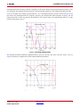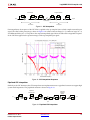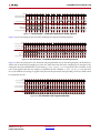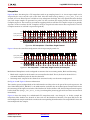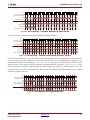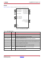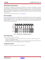
1
LogiCORE IP CIC Compiler v3.0
DS845 June 22, 2011
Product Specification
Introduction
LogiCORE IP Facts Table
The Xilinx ® LogiCORE™ IP CIC Compiler core
provides the ability to design and implement
AXI4-Stream-compliant Cascaded Integrator-Comb
(CIC) filters.
Core Specifics
Supported
Device Family(1)
Virtex-7, Kintex-7, Artix™-7, Zynq™-7000,
Virtex-6, Spartan-6,
Supported User
Interfaces
AXI4-Stream
Provided with Core
Features
Documentation
•
AXI4-Stream-compliant interfaces
Design Files
•
Decimation or interpolation
Example Design
•
Fixed or programmable rate change from 4 to 8192
Test Bench
•
Three to six CIC stages
Constraints File
•
One or two differential delays
Simulation
Model
•
Support of signed, two’s complement input data
from 2 bits to 24 bits
•
Full or limited precision output data
•
Single or multichannel support for up to 16
channels
•
Hardware folding for small footprint
implementations
•
Optional mapping to XtremeDSP™ Slices
•
Synchronous clear input
•
Clock enable input
•
Use with Xilinx CORE Generator™ software and
Xilinx System Generator for DSP v13.2
Product Specification
Netlist
Not Provided
VHDL
N/A
VHDL and Verilog
Tested Design Tools
Design Entry
Tools
CORE Generator 13.2
System Generator for DSP 13.2
Simulation(2)
Mentor Graphics ModelSim
Cadence Incisive Enterprise Simulator (IES)
Synopsys VCS and VCS MX
ISim
Synthesis Tools
XST 13.2
Support
Provided by Xilinx, Inc.
1.
2.
For a complete listing of supported devices, see the release notes for this
core.
For the supported version of the tools, see the ISE Design Suite 13:
Release Notes Guide
© Copyright 2011. Xilinx, Inc. Xilinx, the Xilinx logo, Artix, ISE, Kintex, Spartan, Virtex, Zynq, and other designated brands included herein are trademarks of Xilinx in
the United States and other countries. MATLAB and Simulink are registered trademarks of The MathWorks, Inc. ARM is a registered trademark of ARM in the EU and
other countries. The AMBA trademark is a registered trademark of ARM Limited. All other trademarks are the property of their respective owners.
DS845 June 22, 2011
Product Specification
www.xilinx.com
1
LogiCORE IP CIC Compiler v3.0
Overview
Cascaded Integrator-Comb (CIC) filters, also known as Hogenauer filters, are multirate filters often used for
implementing large sample rate changes in digital systems. They are typically employed in applications that have
a large excess sample rate. That is, the system sample rate is much larger than the bandwidth occupied by the
processed signal as in digital down converters (DDCs) and digital up converters (DUCs). Implementations of CIC
filters have structures that use only adders, subtractors, and delay elements. These structures make CIC filters
appealing for their hardware-efficient implementations of multirate filtering.
Theory of Operation
The following description of the CIC decimator and interpolator is based closely on that provided in [Ref 1]. The
general concept of a CIC filter is the low-pass response that results from filtering an input signal with a cascade of
N unit-amplitude, rectangular windows of length R*M. The system response of such filter is
H ( z) = [
R*M −1
∑z
−k
]N
k =0
or
Equation 1
H ( z) =
− R *M
(1 − z
)
−1 N
(1 − z )
N
where
N is the number of CIC stages
R is the rate change (decimation or interpolation)
M is the differential delay in the comb section stages of the filter
The implementation of this filter response with a clever combination of comb filter sections, integrator sections, and
up-sampling (for interpolation) and down-sampling (for decimation) gives rise to the hardware-efficient
implementation of CIC filters.
DS845 June 22, 2011
Product Specification
www.xilinx.com
2
LogiCORE IP CIC Compiler v3.0
Frequency Response Characteristics
The frequency response of a CIC filter is obtained by evaluating Equation 1 at:
z = e 2 jπf
Equation 2
Where f is the discrete-time frequency, normalized to the higher frequency in a rate changing filter - input sampling
frequency in a CIC decimation, or output sampling frequency in a CIC interpolator. Evaluating Equation 1 in the
z-plane at the sample points defined by Equation 2 gives a magnitude frequency response as shown in Equation 3.
⎡ sin(πRMf ) ⎤
H( f ) = ⎢
⎥
⎣ sin(πf ) ⎦
N
Equation 3
This magnitude response is low-pass. In the design process of a CIC filter implementation, the parameters R, M,
and N are selected to provide adequate passband characteristics over the frequency range from zero to a
predetermined cutoff frequency fc. This passband frequency range is typically the bandwidth of interest occupied
by the signal undergoing processing by the CIC filter. Figure 1 shows the frequency response of a 3-stage (N = 3)
CIC filter with unity differential delay (M = 1) and a sample rate change R = 7.
According to Equation 3 and as seen in Figure 1, there are nulls in the magnitude response (transfer function zeros)
at integer multiples of f =1/(RM). Thus, the differential delay parameter, M, can be used as a design parameter to
control the placement of the nulls.
X-Ref Target - Figure 1
Figure 1: CIC Magnitude Response
DS845 June 22, 2011
Product Specification
www.xilinx.com
3
LogiCORE IP CIC Compiler v3.0
Figure 2 shows the effect of the differential delay M on the magnitude response of a filter with three stages (N = 3)
and a sample rate change R = 7. Besides the effect on the placement of the response nulls, increasing M also
increases the amount of attenuation in side lobes of the magnitude response.
X-Ref Target - Figure 2
Figure 2: CIC Magnitude Response – Effect of Differential Delay M
The rate change parameter R can also be used to control the frequency response of the CIC filter. The effect of R on
the magnitude response can be seen in Figure 3. In essence, increasing the rate change increases the length of the
cascaded unit-amplitude, rectangular window of length R*M. This results in an increase in attenuation and
decrease of the width of the response side lobes.
X-Ref Target - Figure 3
Figure 3: CIC Magnitude Response – Effect of Rate Change R
DS845 June 22, 2011
Product Specification
www.xilinx.com
4
LogiCORE IP CIC Compiler v3.0
The number of stages parameters, N, can also be used to affect the CIC filter magnitude response. This effect can be
understood from the fundamental concept of a cascade of N filtering stages, each with an impulse response of a
unit-amplitude, rectangular window. The larger the number of cascaded stages, the more attenuated the magnitude
response side lobes become. This can be seen in Figure 4.
X-Ref Target - Figure 4
Figure 4: CIC Magnitude Response – Effect of Number of Stages N
Increasing N has the effect of increasing the order of the zeros in the frequency response. This, in turn, increases the
attenuation at frequencies in the locality of the zero. This effect is clearly illustrated in Figure 4 where we see
increasing attenuation of the filter side lobes as N is increased.
As the order of the zeros increase, the passband droop also increases, thus narrowing the filter bandwidth. The
increased droop might not be acceptable in some applications. The droop is frequently corrected using an
additional (non-CIC-based) stage of filtering after the CIC decimator. In the case of a CIC interpolator, the signal can
be pre-compensated to account for the impact in the passband as the signal is up-sampled by the CIC interpolator.
DS845 June 22, 2011
Product Specification
www.xilinx.com
5
LogiCORE IP CIC Compiler v3.0
A compensation filter (not part of the CIC Compiler) can be used to flatten the passband frequency response. For a
CIC decimator, the compensation filter operates at the decimated sample rate. The compensation filter provides
(x/ sin(x))N shaping. An example of a third order (N = 3) R = 64 compensated CIC system is shown in Figure 5. The
plot shows the uncompensated CIC frequency response, the compensation filter frequency response, and the
compensated CIC. In this case, because the number of CIC stages is three, the compensation filter has a cubic
response of the form (x/sin(x))3.
X-Ref Target - Figure 5
Figure 5: CIC Droop Compensation
The compensation filter coefficients employed were [-1, 4, 16, 32, –64, 136, –352, 1312, –352, 136, –64, 32, –16, 4, -1].
Figure 6 provides an exploded view of the compensated filter passband.
X-Ref Target - Figure 6
Figure 6: CIC Droop Compensation – Exploded View
DS845 June 22, 2011
Product Specification
www.xilinx.com
6
LogiCORE IP CIC Compiler v3.0
CIC Decimator
When the output of the filter given by Equation 1 is decimated (down-sampled) by a factor R, the response of the
filter referenced to the lower, down-sampled output rate is expressed in Equation 4 as:
H ( z) =
(1 − z − M ) N
(1 − z −1 ) N
Equation 4
This response can be viewed as a cascade of N integrators and N comb filters.
H ( z) =
1
* (1 − z − M ) N
−1 N
(1 − z )
Equation 5
A block diagram of a realization of this response can be seen in Figure 7. There are two sections to the CIC
decimator filter: an integrator section with N integrator stages that processes input data samples at a sampling rate
fs, and a comb section that operates at the lower sampling rate fs / R. This comb section consists of N comb stages
with a differential delay of M samples per stage. The down sampling operation decimates the output of the
integrator section by passing only every Rth sample to the comb section of the filter.
X-Ref Target - Figure 7
Integrator Section
Z -1
SIgIn
+
Comb Section
Z -1
Z -1
...
+
Z -M
+
Downsampling by R
Z
+
+
...
-M
+
+
Z -M
+
+
SigOut
N comb filters
N integrators
Figure 7: CIC Decimation Filter
Referring back to Figure 1, when the CIC filter is employed as a decimator, the frequency bands in the interval
k
⎢R⎥
± f c , k = 1,2,...⎢ ⎥
RM
⎣2⎦
Equation 6
alias back into the filter passband. Care must be taken to ensure that the integrated side lobe levels do not impact
the intended application. Figure 8 shows an example of a CIC decimator response prior to down-sampling to help
illustrate the effect of aliasing. In Figure 8, the ideal response of a decimator with sampling rate change of R = 8,
number of stages N = 3, and differential delay M = 1 is shown. The spectrum of the decimator input is also shown
containing energy in the intended passband (low frequencies up to a cutoff frequency fc = 1/32 cycles/sample) and
in the stopband (around 1/4 cycles/sample). The output of the decimator (without down-sampling) is shown to
demonstrate the attenuation produced by this CIC filter. The dashed vertical lines in Figure 8 indicate the frequency
ranges that alias to the passband when down-sampling. In this figure, the frequency axis is normalized to the
(higher) sampling frequency prior to down-sampling.
DS845 June 22, 2011
Product Specification
www.xilinx.com
7
LogiCORE IP CIC Compiler v3.0
X-Ref Target - Figure 8
Figure 8: CIC Decimator Response before Down-sampling
Figure 9 shows the output spectrum of the CIC decimator example. In Figure 9, the frequency axis is normalized
relative to the lower sampling rate obtained after down-sampling. Because of this re-normalization of frequencies,
the plots in Figure 9 can be conceptualized as a zoomed view of the frequency range from 0 to 1/(2*R) = 1/16
cycles/sample of Figure 8.
X-Ref Target - Figure 9
Figure 9: CIC Decimator Output Spectrum
DS845 June 22, 2011
Product Specification
www.xilinx.com
8
LogiCORE IP CIC Compiler v3.0
The important points to note from Figure 9 are:
•
The solid red plot shows the CIC output spectrum if no aliasing occurred.
•
The dashed red plot shows the stopband output spectrum when aliased due to down-sampling. This aliased
spectrum affects the final output of the CIC decimator by contributing additively to the output spectrum.
•
The solid blue plot is the actual output of the CIC decimator which clearly shows the contribution of the
aliased spectrum from down-sampling.
Again, care must be taken to ensure that the CIC decimator parameters are properly chosen to avoid detrimental
effects from aliasing.
Pipelined CIC Decimator
To support high system clock frequencies, the CIC decimator is implemented using the pipelined architecture
shown in Figure 10.
X-Ref Target - Figure 10
Pipelined
Integrator
Section
Pipelined
Comb Section
Z -M
SIgIn
Z -1
+
Z -1
+
Z -1
...
+
Z -1
+
Downsampling
by R
Z
Z -1
-M
...
+
Z -M
+
+
Z -1
+
Z -1
SigOut
+
Figure 10: Pipelined CIC Decimator
Register Growth in CIC Decimator
The CIC datapath undergoes internal register growth that is a function of all the design parameters: N, M, R in
addition to the input sample precision B. As shown in [Ref 1], the output bit width of a CIC decimator with full
precision is given by
Bmax = ⎡N log 2 RM + B ⎤
Equation 7
where ⎡ ⎤ denotes the ceiling operator. The CIC Compiler supports both full and limited precision output. For full
precision, the CIC decimator implementation uses Bmax bits internally for each of the integrator and differentiator
stages. This introduces no quantization error at the output. For limited precision (that is, output bit width less than
Bmax), the registers in the integrator and comb stages are sized to limit the quantization noise variance at the output
as described in [Ref 1]. Consequently, the hardware resources in a CIC decimator implementation can be reduced
when using limited precision output at the cost of quantization noise. This ability to trade off resources and
quantization noise is important to achieve an optimum implementation.
CIC Interpolator
The structure for a CIC interpolator filter is shown in Figure 11. This structure is similar to that of a CIC decimator
with the integrator and comb sections in reverse order. In this case, there is an up-sampling of data by a factor, R,
between the comb and integrator sections. This rate increase is done by inserting R-1 zero-valued samples between
consecutive samples of the comb section output. The up-sampled and filtered data stream is output at the sample
rate fs.
DS845 June 22, 2011
Product Specification
www.xilinx.com
9
LogiCORE IP CIC Compiler v3.0
X-Ref Target - Figure 11
Comb Section
Z -M
Z -M
-
SIgIn
+
+
Integrator Section
Z -M
-
...
+
+
Z -1
+
+
+
Z
-1
Z -1
...
+
SigOut
+
Upsampling R
N integrators
N comb filters
Figure 11: CIC Interpolator
For interpolation, the response of the CIC filter is applied to the up-sampled (zero-valued samples inserted) input
signal. The effect of this processing is shown in Figure 12 in a filter with rate change R = 7, number of stages N = 4,
and differential delay M = 1. The peaks in the output interpolated signal show the effect of the magnitude response
of the CIC filter applied to the spectrum images of the up-sampled input signal.
X-Ref Target - Figure 12
Figure 12: CIC Interpolator Response
Pipelined CIC Interpolator
Similarly to the CIC decimator, the CIC interpolator core implementation uses a pipelined structure to support high
system clock frequencies. This pipelined structure is shown in Figure 13.
X-Ref Target - Figure 13
Pipelined
Comb Section
Z -M
SIgIn
Z -1
+
+
Z -M
Z -1
...
+
+
Z
-
Pipelined
Integrator
Section
-M
-
Z -1
+
Z -1
Z
+
Upsampling
by R
-1
+
Z -1
+
+
+
Z -1
...
+
Z -1
SigOut
+
Figure 13: Pipelined CIC Interpolator
DS845 June 22, 2011
Product Specification
www.xilinx.com
10
LogiCORE IP CIC Compiler v3.0
Register Growth in CIC Interpolator
The datapath in a CIC interpolator also undergoes internal register growth that is a function of all the design
parameters: N, M, R, in addition to the input sample precision B. As shown in [Ref 1], the registers in the comb and
integrator sections grow monotonically with the maximum register size occurring at the output of the last stage
(output of the CIC filter). The maximum register width is given by Equation 8:
⎡
⎤
( RM ) N
Bmax = ⎢log 2
+ B⎥
R
⎢
⎥
Equation 8
where ⎡ ⎤ denotes the ceiling operator. The CIC Compiler always sizes the internal stage registers according to the
register growth as described in [Ref 1]. The output of the filter can be selected to be full or limited precision (with
truncation or rounding) to accommodate an output width specific to an application. Using limited precision does
not affect the internal register sizes and only the final stage output is scaled, and rounded if desired, to provide the
selected output width.
Output Width and Gain
As illustrated by Equation 7 and Equation 8, the gain of a CIC filter is a function of all the key design parameters.
When the output width is equal to the maximum register width, the core outputs the full precision result and the
magnitude of the core output reflects the filter gain. When the output width is set to less than the maximum register
width, the output is truncated with a corresponding reduction in gain.
When the core is configured to have a programmable rate change, there is a corresponding change in gain as the
filter rate is changed. When the output is specified to full precision, the change in gain is apparent in the core output
magnitude as the rate is changed. When the output is truncated, the core shifts the internal result, given the Bmax for
the current rate change, to fully occupy the output bits.
Control Signals and Timing
Symbol data to be processed is loaded into the CIC Compiler core using the Data Input Channel. Processed symbol
data is unloaded using the Data Output Channel. Both of these use the AXI4-Stream protocol. Figure 14 shows the
basics of this protocol.
TVALID is driven by the channel master to show that it has data to transfer, and TREADY is driven by the channel
slave to show that it is ready to accept data. When both TVALID and TREADY are high, a transfer takes place.
Points A in the diagram show clock cycles where no data is transferred because neither the master or the slave is
ready. Point B shows two clock cycles where data is not transferred because the Master does not have any data to
transfer. This is known as a master waitstate. Point C shows a clock cycle where no data is transferred because the
slave is not ready to accept data. This is known as a slave waitstate. Master and slave waitstates can extend for any
number of clock cycles.
DS845 June 22, 2011
Product Specification
www.xilinx.com
11
LogiCORE IP CIC Compiler v3.0
X-Ref Target - Figure 14
ACLK
TVALID
A
B
A
TREADY
TDATA
C
D1
D2
D3
D4
D5
D6
D7
D8
Figure 14: AXI Transfers and Terminology
When the master asserts TVALID high, it must remain asserted (and the associated data remain stable) until the
slave asserts TREADY high.
Figure 14 shows the loading of 8 samples. The upstream master drives TVALID and the CIC Compiler drives
TREADY. In this case, both the master and the CIC Compiler insert waitstates.
Figure 14 also shows the unloading of 8 samples. The CIC Compiler drives TVALID and the downstream slave
drives TREADY. In this case, both the CIC Compiler and the slave insert waitstates. This only applies when the core
is configured to have a TREADY port on the Data Output Channel (XCO HAS_DOUT_TREADY = true). When this
is false, there is no TREADY signal on the Data Output Channel and the downstream slave cannot insert waitstates.
The slave must be able to respond immediately on every clock cycle where the CIC Compiler produces data
(m_axis_data_tvalid asserted high). If the slave cannot respond immediately, then data is lost.
For multiple-channel implementations, the CIC Compiler core supports time-multiplexed input and output. The
filter input data in the DATA field of the Data Input Channel's TDATA vector (s_axis_data_tdata) is expected
to have an ordered, time-multiplexed format. The core produces time-multiplexed output data on the DATA field of
the Data Output Channel's TDATA vector (m_axis_data_tdata). Two additional fields are included in
multichannel implementation. The CHAN_SYNC field in the Data Output Channel's TUSER vector
(m_axis_data_tuser) indicates the output corresponding to the first channel in the time-multiplexed stream.
The CHAN_OUT field in the Data Output Channel's TUSER vector (m_axis_data_tuser) contains the channel
number for each output in the time-multiplexed steam.
For programmable rate implementations, the RATE field in the Configuration Channel's TDATA vector
(s_axis_config_tdata) controls the rate change in the CIC Compiler filter core. The RATE field is sampled
when s_axis_config_tvalid and s_axis_config_tready are both asserted high. The core uses the new
RATE value on the next input sample, for a single channel implementation, or the next input to the first channel, for
multiple channel implementations.
All of the waveforms (Figure 15 to Figure 24) are shown with HAS_DOUT_TREADY = false. Setting this to true
allows the downstream data slave to delay the data output of the CIC Compiler. It also allows the Data Input
Channel to buffer samples so that they can be supplied at a faster rate than the core can process them.
To simplify the waveforms, the following field aliases are used:
•
DIN is used to represent the DATA field in the Data Input Channel's TDATA vector (s_axis_data_tdata)
•
DOUT is used to represent the DATA field in the Data Output Channel's TDATA vector (m_axis_data_tdata)
•
CHAN_SYNC is used to represent the CHAN_SYNC field in the Data Output Channel's TUSER vector
(m_axis_data_tuser)
•
CHAN_OUT is used to represent the CHAN_OUT field in the Data Output Channel's TUSER vector
(m_axis_data_tuser)
•
RATE is used to represent the RATE field in the Configuration Channel's TDATA vector (s_axis_config_tdata)
DS845 June 22, 2011
Product Specification
www.xilinx.com
12
LogiCORE IP CIC Compiler v3.0
Decimator
The timing for a CIC decimator with a down-sampling factor R = 4 is shown in Figure 15. In this example, the core
is not oversampled and can accept a new input sample on every clock edge. Some number of clock cycles after the
first input sample has been written to the filter, m_axis_data_tvalid is asserted by the filter to indicate that the
first output sample is available. This time interval is a function of the down-sampling factor R and a fixed latency
that is related to internal pipeline registers in the core. The number of pipeline stages depends on the core
parameters. After the first output sample has been produced, subsequent outputs are available every R clock cycles.
X-Ref Target - Figure 15
ACLK
S_AXIS_DATA_TREADY
S_AXIS_DATA_TVALID
DIN
x0
x1
x2
x3
x4
x5
M_AXIS_DATA_TVALID
DOUT
y0
y1
y2
y3
Figure 15: CIC Decimator – Fixed Rate, Single Channel
Figure 16 shows the timing for the same filter configuration with an input sample period of 3. At point A in the
waveform, the CIC Compiler is ready to accept data but the master does not provide it. The CIC Compiler continues
to ask until it is provided (point B). At point C in the waveform, the master provides data before the CIC Compiler
requests it. The master has to continue supplying this data until the CIC Compiler accepts it (at point D).
X-Ref Target - Figure 16
ACLK
S_AXIS_DATA_TREADY
A
B
input sample period
S_AXIS_DATA_TVALID
C
DIN
x0
x1
x2
x3
x4
D
x5
M_AXIS_DATA_TVALID
output sample period
DOUT
y0
y1
y2
Figure 16: CIC Decimator – Fixed Rate, Single Channel, Oversampled
Multichannel Decimators can be configured to produce data in two timing modes, Block and Streaming:
•
Block mode: samples for the channels are produced back-to-back. That is, the data for channel N+1 is
produced immediately after the data for channel N.
•
Streaming mode: samples for the channels are produced evenly over the entire sample period.
See Figure 18 and Figure 19 more information.
These modes operate independently of the AXI4 interface and they refer to the part of the core that processes the
data. When HAS_DOUT_TREADY = 1 the AXI4 interface can buffer data in the Data Output Channel which means
that streaming mode can start to behave like block mode. If the downstream system does not consume data when
it first becomes available, the Data Output Channel can start to fill. In this case, the Data Output Channel produces
back-to-back data (using m_axis_data_tvalid) until the buffer in the channel is empty, even though the
processing part of the core did not produce it back-to-back.
Figure 17 shows the timing for a multichannel CIC decimator with a rate change R = 4. In this example the
decimator filter handles three channels of data and is configured to use the block-based interface. The input to the
decimator DIN shows the time-multiplexed samples with labels to indicate the corresponding channel number. The
output of the decimator DOUT shows the time-multiplexed data.
DS845 June 22, 2011
Product Specification
www.xilinx.com
13
LogiCORE IP CIC Compiler v3.0
X-Ref Target - Figure 17
ACLK
S_AXIS_DATA_TREADY
S_AXIS_DATA_TVALID
DIN
ch0x0
ch1x0
ch2x0
ch0x1
ch1x1
ch2x1
ch0x2
ch1x2
ch2x2
ch0y0
ch1y0
ch2y0
ch0y1
ch1y1
ch2y1
0
1
2
0
1
2
S_AXIS_DATA_TLAST
M_AXIS_DATA_TVALID
DOUT
CHAN_SYNC
CHAN_OUT
M_AXIS_DATA_TLAST
Figure 17: CIC Decimator – Fixed Rate, Multichannel, Block interface
Figure 18 shows the timing for the same filter configuration using the streaming interface.
X-Ref Target - Figure 18
ACLK
S_AXIS_DATA_TREADY
S_AXIS_DATA_TVALID
DIN
ch0x0
ch1x0
ch2x0
ch0x1
ch1x1
ch2x1
ch0x2
ch1x2
ch2x2
S_AXIS_DATA_TLAST
M_AXIS_DATA_TVALID
DOUT
ch0y0
ch1y0
ch2y0
ch0y1
ch1y1
ch2y1
0
1
2
0
1
2
CHAN_SYNC
CHAN_OUT
M_AXIS_DATA_TLAST
Figure 18: CIC Decimator – Fixed Rate, Multichannel, Streaming interface
Figure 19 shows the timing for a CIC decimator with programmable rate. In the timing diagram, the decimator is
shown with an initial down-sampling rate value of 4. After some time, the down sampling rate is changed to 7 by
setting the value in the RATE field to 7 and asserting s_axis_config_tvalid at point A in the waveform. As the
rate is only applied when the next sample is accepted by the CIC Compiler, s_axis_config_tready deasserts
for a cycle while the rate change is applied. This prevents the upstream master providing a new rate which cannot
be accepted by the core.
X-Ref Target - Figure 19
ACLK
S_AXIS_DATA_TREADY
S_AXIS_DATA_TVALID
DIN
x0
x1
x2
x3
x4
S_AXIS_CONFIG_TVALID
S_AXIS_CONFIG_TREADY
A
RATE
7
M_AXIS_DATA_TVALID
DOUT
y0
y1
y2
y3
y4
Figure 19: CIC Decimator with Programmable Rate
DS845 June 22, 2011
Product Specification
www.xilinx.com
14
LogiCORE IP CIC Compiler v3.0
Interpolator
Figure 20 shows the timing for a CIC interpolator with an up-sampling factor R = 4. A new input sample can be
accepted by the core every 4th cycle of the clock. After the initial start-up latency, m_axis_data_tvalid is
asserted, and a new filter output is available on every subsequent clock edge. For every input delivered to the filter
core, four output samples are generated. At point A in the waveform, the master provides data before the CIC
Compiler requests it. The master has to continue supplying this data until the CIC Compiler accepts it (at point B).
At point C in the waveform, the CIC Compiler is ready to accept data but the master does not provide it. The CIC
Compiler continues to ask until it is provided (point D).
X-Ref Target - Figure 20
ACLK
S_AXIS_DATA_TREADY
C
S_AXIS_DATA_TVALID
DIN
A
x1
x0
D
B
x2
x3
x4
x5
M_AXIS_DATA_TVALID
DOUT
y0
y1
y2
y3
Figure 20: CIC Interpolator – Fixed Rate, Single Channel
Figure 21 shows the same filter configuration with an input sample period of 8.
X-Ref Target - Figure 21
ACLK
S_AXIS_DATA_TREADY
S_AXIS_DATA_TVALID
DIN
x0
x1
x2
M_AXIS_DATA_TVALID
DOUT
y0
y1
y2
y3
Figure 21: CIC Interpolator – Fixed Rate, Single Channel, Oversampled
Multichannel Interpolators can be configured to consume data in two timing modes, Block and Streaming:
•
Block mode: samples for the channels are consumed back-to-back. That is, the data for channel N+1 is
consumed immediately after the data for channel N.
•
Streaming mode: samples for the channels are consumed evenly over the entire sample period
See Figure 22 and Figure 23 for more information.
These modes operate independently of the AXI4 interface and they refer to the part of the core that processes the
data. When HAS_DOUT_TREADY = 1 the AXI4 interface can buffer data in the Data Input Channel which means
that streaming mode might start to behave like block mode. Until its buffer is full, the Data Input Channel requests
back-to-back data (using s_axis_data_tready) even though the processing part of the core does not consume it
immediately.
Figure 22 shows the timing for a multichannel CIC interpolator with a rate change R = 4. In this example the
interpolator filter handles two channels of data and uses the block-based interface. The input DIN shows the
time-multiplexed samples with labels to indicate the corresponding channel number. The output DOUT shows the
time-multiplexed data samples.
DS845 June 22, 2011
Product Specification
www.xilinx.com
15
LogiCORE IP CIC Compiler v3.0
X-Ref Target - Figure 22
ACLK
S_AXIS_DATA_TREADY
S_AXIS_DATA_TVALID
DIN
ch0x0
ch1x0
ch0x1
ch1x1
ch0x2
ch1x2
S_AXIS_DATA_TLAST
M_AXIS_DATA_TVALID
DOUT
ch0y0
ch1y0
ch0y1
ch1y1
ch0y2
ch1y2
ch0y3
ch1y3
ch0y4
ch1y4
ch0y5
ch1y5
ch0y6
ch1y6
ch0y7
ch1y7
0
1
0
1
0
1
0
1
0
1
0
1
0
1
0
1
CHAN_SYNC
CHAN_OUT
M_AXIS_DATA_TLAST
Figure 22: CIC Interpolator – Fixed Rate, Multichannel, Block interface
Figure 23 shows the same filter configuration using the streaming interface.
X-Ref Target - Figure 23
ACLK
S_AXIS_DATA_TREADY
S_AXIS_DATA_TVALID
DIN
ch0x0
ch1x0
ch0x1
ch1x1
ch0x2
ch1x2
S_AXIS_DATA_TLAST
M_AXIS_DATA_TVALID
DOUT
ch0y0
ch1y0
ch0y1
ch1y1
ch0y2
ch1y2
ch0y3
ch1y3
ch0y4
ch1y4
ch0y5
ch1y5
ch0y6
ch1y6
ch0y7
ch1y7
0
1
0
1
0
1
0
1
0
1
0
1
0
1
0
1
CHAN_SYNC
CHAN_OUT
M_AXIS_DATA_TLAST
Figure 23: CIC Interpolator – Fixed Rate, Multichannel, Streaming interface
Figure 24 shows the timing for a CIC interpolator with programmable rate. In the timing diagram, the interpolator
is shown with an initial up-sampling rate value of 4. After some time, the up-sampling rate is changed to 7 by
setting the RATE field to 7 and asserting s_axis_config_tvalid at point A in the waveform. As the rate is only
applied when the next sample for the first channel is accepted by the CIC Compiler, s_axis_config_tready
deasserts until the rate change is applied (point B). In this example, the sample (x1) following point A is for the
second channel, so the rate is not applied here. This prevents the upstream master providing a new rate which
cannot be accepted by the core.
X-Ref Target - Figure 24
ACLK
S_AXIS_DATA_TREADY
S_AXIS_DATA_TVALID
DIN
x0
x1
x0
x1
S_AXIS_CONFIG_TVALID
S_AXIS_CONFIG_TREADY
A
RATE
7
B
M_AXIS_DATA_TVALID
DOUT
y0
y1
y2
y3
y4
y0
y1
Figure 24: CIC Interpolator with Programmable Rate
DS845 June 22, 2011
Product Specification
www.xilinx.com
16
LogiCORE IP CIC Compiler v3.0
Pinout
Figure 25 and Table 1 illustrate and define the schematic symbol signal names.
X-Ref Target - Figure 25
S?AXIS?DATA?TVALID
M?AXIS?DATA?TVALID
S?AXIS?DATA?TREADY
M?AXIS?DATA?TREADY
S?AXIS?DATA?TDATA
M?AXIS?DATA?TDATA
M?AXIS?DATA?TUSER
S?AXIS?DATA?TLAST
M?AXIS?DATA?TLAST
S?AXIS?CONFIG?TVALID
S?AXIS?CONFIG?TREADY
S?AXIS?CONFIG?TDATA
EVENT?TLAST?MISSING
EVENT?TLAST?UNEXPECTED
EVENT?HALTED
ACLK
ARESETN
ACLKEN
$3??
Figure 25: Core Schematic Symbol
Table 1: Core Signal Pinout
Name
Direction
Description
aclk
Input
Rising edge clock
aclken
Input
Active high clock enable (optional).
aresetn
Input
Active low synchronous clear (optional, always take priority over aclken).
A minimum aresetn active pulse of two cycles is required.
s_axis_config_tvalid
Input
TVALID for the Configuration Channel.
Asserted by the external master to signal that it is able to provide data.
s_axis_config_tready
Output
s_axis_config_tdata
Input
TDATA for the Configuration Channel.
Carries the configuration information: RATE.
s_axis_data_tvalid
Input
TVALID for the Data Input Channel.
Used by the external master to signal that it is able to provide data.
s_axis_data_tready
Output
TREADY for the Data Input Channel.
Used by the CIC Compiler to signal that it is ready to accept data.
s_axis_data_tdata
Input
DS845 June 22, 2011
Product Specification
TREADY for the Configuration Channel.
Asserted by the CIC Compiler to signal that it is ready to accept configuration data.
TDATA for the Data Input Channel.
Carries the unprocessed sample data.
www.xilinx.com
17
LogiCORE IP CIC Compiler v3.0
Table 1: Core Signal Pinout (Cont’d)
Name
s_axis_data_tlast
Direction
Input
Description
TLAST for the Data Input Channel.
Only present in multichannel mode.
Asserted by the external master on the sample corresponding to the last channel.
This is not used by the CIC Compiler except to generate the events
event_tlast_unexpected and event_tlast_missing events
m_axis_data_tvalid
Input
TVALID for the Data Output Channel.
Asserted by the CIC Compiler to signal that it is able to provide sample data.
m_axis_data_tready
Output
m_axis_data_tdata
Input
TDATA for the Data Output Channel.
Carries the processed sample data
m_axis_data_tuser
Input
TUSER for the Data Output Channel.
Only present in multichannel mode.
TREADY for the Data Output Channel.
Asserted by the external slave to signal that it is ready to accept data. Only present
when the XCO parameter HAS_DOUT_TREADY is true.
Carries additional per-sample information:
CHAN_OUT
CHAN_SYNC
m_axis_data_tlast
Input
TLAST for the Data Output Channel.
Only present in multichannel mode.
Asserted by the CIC Compiler on the sample corresponding to the last channel.
event_tlast_missing
Output
Asserted when s_axis_data_tlast is not asserted on the data sample corresponding to
the last channel.
Only present in multichannel mode.
event_tlast_unexpected
Output
Asserted when s_axis_data_tlast is asserted on a data sample that does not
correspond to the last channel.
Only present in multichannel mode.
event_halted
Output
Asserted when the CIC Compiler tries to write data to the Data Output Channel and it
is unable to do so.
Only present when the XCO HAS_DOUT_TREADY is true.
CORE Generator Graphical User Interface
The CIC Compiler core GUI has three pages used to configure the core plus three informational/analysis tabs.
Tab 1: IP Symbol
The IP Symbol tab illustrates the core pinout.
DS845 June 22, 2011
Product Specification
www.xilinx.com
18
LogiCORE IP CIC Compiler v3.0
Tab 2: Frequency Response
The Freq. Response tab (Figure 26), the default tab when the CORE Generator software is started, displays the filter
frequency response (magnitude only). The content of the tab can be adjusted to fit the entire window or un-docked
(as shown) into a separate window.
X-Ref Target - Figure 26
Figure 26: Frequency Response tab
It is important to note that the frequency axis in this plot is also normalized frequency as in other plots shown in this
data sheet. Although the values in the GUI plot range from 0 to 1.0, they represent the same range of frequencies as
in the other figures, that is, the range from 0 to 1/2 the sampling frequency. It is also important to note that the
normalizing sampling frequency implied in the GUI plot depends on the type of filter. For a CIC decimator, the
normalizing sampling frequency is the higher, input sampling frequency. For a CIC interpolator, the normalizing
frequency is the higher, output sampling frequency.
•
Response Magnitude: Specifies the magnitude scaling of the frequency response: Normalized; Full Precision
(the absolute filter gain) and Output Quantization (the effective filter gain given the core output width). In
previous versions of the core, the frequency response was always normalized. All plots shown in Theory of
Operation, page 2 use normalized magnitude.
•
Passband Range: Two fields are available to specify the passband range, the left-most being the minimum
value and the right-most the maximum value. The values are specified in the same units as on the graph x-axis
(for example, normalized to pi radians per second). For the specified range, the passband maximum,
minimum and ripple values are calculated and displayed (in dB).
•
Stopband Range: Two fields are available to specify the stopband range, the left-most being the minimum
value and the right-most the maximum value. The values are specified in the same units as on the graph x-axis
(for example, normalized to pi radians per second). For the specified range, the stopband maximum value is
calculated and displayed (in dB).
Note: The user can specify any range for the passband or stopband, allowing closer analysis of any region of the response.
DS845 June 22, 2011
Product Specification
www.xilinx.com
19
LogiCORE IP CIC Compiler v3.0
Tab 3: Implementation Details
Resource Estimates
Based on the options selected, this field displays the XtremeDSP slice count and 18K block RAM numbers (9K block
RAM numbers for Spartan ®-6 devices). The resource numbers are an estimate; for exact resource usage, and
slice/LUT-FlipFlop pair information, a MAP report should be consulted.
AXI4-Stream Port Structure
This section shows how the CIC Compiler’s fields are mapped to the AXI4 channels. This information can be copied
to the clipboard and pasted as plain text into other applications.
Filter Specification
•
Component Name: The name of the core component to be instantiated. The name must begin with a letter and
be composed of the following characters: a to z, 0 to 9, and “_”.
•
Filter Type: The CIC Compiler core supports both interpolator and decimator types. When the filter type is
selected as decimator, the input sample stream is down-sampled by the factor R. When an interpolator is
selected, the input sample is up-sampled by R.
•
Number of Stages: Number of integrator and comb stages. If N stages are specified, there are N integrators
and N comb stages in the filter. The valid range for this parameter is 3 to 6.
•
Differential Delay: Number of unit delays employed in each comb filter in the comb section of either a
decimator or interpolator. The valid range of this parameter is 1 or 2.
•
Number of Channels: Number of channels to support in implementation. The valid range of this parameter is
1 to 16
•
Fixed/Programmable: Type of rate change is fixed or programmable.
•
Fixed or Initial Rate: Rate change factor (for fixed type) or initial rate change factor (for programmable type).
For an interpolation filter, the rate change specifies the amount of up-sampling. For a decimator, it specifies the
amount of down-sampling.
•
Minimum Rate: Minimum rate change factor for programmable rate change.
•
Maximum Rate: Maximum rate change factor for programmable rate change.
•
Hardware Oversampling Specification format: Selects which format is used to specify the hardware
oversampling rate, the number of clock cycles available to the core to process an input sample and generate an
output. This value directly affects the level of parallelism in the core implementation and resources used.
When “Frequency Specification” is selected, the user specifies the Input Sampling Frequency and Clock
Frequency. The ratio between these values along with other core parameters determine the hardware
oversampling rate. When “Sample Period” is selected, the user specifies the integer number of clock cycles
between input samples.
•
Input Sample Frequency: This field can be an integer or real value. It specifies the sample frequency for one
channel. The upper limit is set based on the clock frequency and filter parameters such as interpolation rate
and number of channels.
•
Clock Frequency: This field can be an integer or real value. The limits are set based on the sample frequency,
interpolation rate and number of channels. This field influences architecture choices only; the specified
clock rate might not be achievable by the final implementation.
•
Input Sample Period: Integer number of clock cycles between input samples. When the multiple channels
have been specified, this value should be the integer number of clock cycles between the time division
multiplexed input sample data stream.
DS845 June 22, 2011
Product Specification
www.xilinx.com
20
LogiCORE IP CIC Compiler v3.0
Implementation Options
•
Input Data Width: Number of bits for input data. The valid range of this parameter is 2 to 24.
•
Quantization: Type of quantization for limited precision output, Full Precision or Truncation. This
quantization applies only to the output and is not applied in the intermediate stages of the CIC Compiler filter.
•
Output Data Width: Number of bits for output data. The valid range of this parameter is up to 48 bits with the
minimum value set to the input data width.
•
Use XtremeDSP Slice: Use DSP hardware primitive slices in the filter implementation.
•
Use Streaming Interface: Specifies if a streaming interface is used for multiple channel implementations. See
Decimator, page 13, for further details.
•
Has DOUT TREADY: Specifies if the Data Output Channel has a TREADY
•
ACLKEN: Determines if the core has a clock enable input (aclken).
•
ARESETN: Determines if the core has an active low synchronous clear input (aresetn).
Note:
a.
The signal aresetn always takes priority over aclken, that is, aresetn takes effect regardless of the state
of aclken.
b.
The signal aresetn is active low.
c.
The signal aresetn should be held active for at least 2 clock cycles. This is because, for performance,
aresetn is internally registered before being fed to the reset port of primitives.
Summary
In addition to all the parameterization values of the core, the summary page displays:
•
Bits per Stage: The number of bits used in each of the stages of the CIC Compiler filter implementation. These
numbers are computed based on the register growth analysis presented in [Ref 1].
•
Latency: The input to output latency in the CIC Compiler core implementation. When HAS_DOUT_TREADY
is true then the actual latency might be greater than reported because throughput can be controlled by the
system connected to the Data Output Channel. The value reported by CORE Generator is the minimum
latency.
System Generator for DSP Graphical User Interface
The CIC Compiler core is available through Xilinx System Generator for DSP, a design tool that enables the use of
the model-based design environment, Simulink ® product for FPGA design. The CIC Compiler core is one of the
DSP building blocks provided in the Xilinx blockset for Simulink. The core can be found in the Xilinx Blockset in the
DSP section. The block is called “CIC Compiler v3.0.” See the System Generator User Manual for more information.
This section describes each tab of the System Generator for DSP GUI and details the parameters that differ from the
CORE Generator GUI. See CORE Generator Graphical User Interface, page 18, for detailed information about all
other parameters.
DS845 June 22, 2011
Product Specification
www.xilinx.com
21
LogiCORE IP CIC Compiler v3.0
Tab 1: Filter Specification
The Filter Specification tab is used to define the basic filter configuration as on the Filter Specification, page 20, of
the CORE Generator GUI.
•
Hardware Oversampling Specification format: Selects which method is used to specify the hardware
oversampling rate. This value directly affects the level of parallelism of the core implementation and resources
used. When “Maximum Possible” is selected, the core uses the maximum oversampling given the sample
period of the signal connected to the Data field of the s_axis_data_tdata port. When “Hardware
Oversampling Rate” is selected, the user can specify the oversampling rate. When “Sample Period” is selected,
the core clock is connected to the system clock, and the value specified for the Sample Period parameter sets
the input sample rate the core supports. The Sample Period parameter also determines the hardware
oversampling rate of the core. When “Sample Period” is selected, the core is forced to use the
s_axis_data_tvalid control port. See Decimator, page 13, for more details on the core control ports.
•
Sample Period: Specifies the input sample period supported by the core.
•
Hardware Oversampling Rate: Specifies the hardware oversampling rate to be applied to the core.
Tab 2: Implementation Options
The Implementation tab is used to define implementation options. See Implementation Options, page 21, of the
CORE Generator GUI for details of all the core parameters on this tab.
•
Has ARESETN: Specifies if the core has a reset pin (the equivalent of selecting the Has ARESETN option in the
CORE Generator GUI).
•
Has ACLKEN: Specifies if the core has a clock enable pin (the equivalent of selecting the Has ACLKEN option
in the CORE Generator GUI).
•
Has DOUT TREADY: Specifies if the core has a TREADY pin for the Data Output Channel (the equivalent of
selecting the HAS_DOUT_TREADY option in the CORE Generator GUI)
•
FPGA Area Estimation: See the System Generator documentation for detailed information about this option.
Using the CIC Compiler IP Core
The CORE Generator GUI performs error-checking on all input parameters. Resource estimation and optimum
latency information are also available.
Several files are produced when a core is generated, and customized instantiation templates for Verilog and VHDL
design flows are provided in the .veo and .vho files, respectively. For detailed instructions, see the CORE Generator
software documentation.
Simulation Models
The core has a number of options for simulation models:
•
VHDL behavioral model in the xilinxcorelib library
•
VHDL UNISIM-based structural simulation model
•
Verilog UNISIM-based structural simulation model
The models required can be selected in the CORE Generator software project options.
Xilinx recommends that simulations utilizing UNISIM-based structural models are run using a resolution of 1 ps.
Some Xilinx library components require a 1 ps resolution to work properly in either functional or timing simulation.
The UNISIM-based structural simulation models might produce incorrect results if simulated with a resolution
other than 1 ps. See the “Register Transfer Level (RTL) Simulation Using Xilinx Libraries” section in Chapter 6 of
[Ref 2] for more information. This document is part of the ISE® Software Manuals set available at
www.xilinx.com/support/documentation/dt_ise.htm.
DS845 June 22, 2011
Product Specification
www.xilinx.com
22
LogiCORE IP CIC Compiler v3.0
XCO Parameters
Table 2 defines valid entries for the XCO parameters. Parameters are not case sensitive. Default values are displayed
in bold. Xilinx strongly suggests that XCO parameters are not manually edited in the XCO file; instead, use the
CORE Generator GUI to configure the core and perform range and parameter value checking. The XCO parameters
are useful for defining the interface to other Xilinx tools.
Table 2: XCO Parameters
XCO Parameter
Valid Values
Component_Name
ASCII text using characters: a..z, 0..9 and ‘_’ ; starting with a letter
Filter_Type
Interpolation, Decimation
Number_Of_Stages
3,4,5,6
Differential_Delay
1,2
Number_Of_Channels
1 - 16
Sample_Rate_Changes
Fixed, Programmable
Fixed_Or_Initial_Rate
4 - 8192
Minimum_Rate
4 - 8191
Maximum_Rate
5 - 8192
RateSpecification
Frequency_Specification, Sample_Period
Input_Sample_Frequency
0.000001 - 600.0
Clock_Frequency
0.000001 - 600.0
SamplePeriod
1 - 10000000
Input_Data_Width
2 - 24
Default is 18
Quantization
Full_Precision, Truncation
Output_Data_Width
2 - 104
Use_Xtreme_DSP_Slice
false, true
Use_Streaming_Interface
true, false
HAS_DOUT_TREADY
false, true
HAS_ACLKEN
false, true
HAS_ARESETN
false, true
Demonstration Test Bench
When the core is generated using CORE Generator, a demonstration test bench is created. This is a simple VHDL
test bench that exercises the core.
The demonstration test bench source code is one VHDL file: demo_tb/tb_<component_name>.vhd in the
CORE Generator output directory. The source code is comprehensively commented.
DS845 June 22, 2011
Product Specification
www.xilinx.com
23
LogiCORE IP CIC Compiler v3.0
Using the Demonstration Test Bench
The demonstration test bench instantiates the generated CIC Compiler core. Either the behavioral model or the
netlist can be simulated within the demonstration test bench.
•
Behavioral model: Ensure that the CORE Generator project options are set to generate a behavioral model.
After generation, this creates a behavioral model wrapper named <component_name>.vhd. Compile this file
into the work library (see your simulator documentation for information on how to do this).
•
Netlist: If the CORE Generator project options were set to generate a structural model, a VHDL or Verilog
netlist named <component_name>.vhd or <component_name>.v was generated. If this option was not set,
generate a netlist using the netgen program, for example:
netgen -sim -ofmt vhdl <component_name>.ngc <component_name>_netlist.vhd
Compile the netlist into the work library (see your simulator documentation for more information on how to
do this).
Compile the demonstration test bench into the work library. Then simulate the demonstration test bench. View the
test bench's signals in your simulator's waveform viewer to see the operations of the test bench.
The Demonstration Test Bench in Detail
The demonstration test bench performs the following tasks:
•
Instantiate the core
•
Generate a clock signal
•
Drive the core's clock enable and reset input signals (if present)
•
Drive the core's input signals to demonstrate core features (see following sections for details)
•
Provide signals showing the separate fields of AXI4 TDATA and TUSER signals
The demonstration test bench drives the core's input signals to demonstrate the features and modes of operation of
the core. The test bench drives a sine wave into the CIC core. In multichannel mode, the frequency of the sine wave
increases with each channel. The output of the core shows the same sine wave (or waves in multichannel mode) but
in a decimated or interpolated format. Alias signals are used to decode the AXI4 channels and allow easy viewing
of the input and output data.
The operations performed by the demonstration test bench are appropriate for the configuration of the generated
core, and are a subset of the following operations (in order):
1.
Asserts reset at the start of the test. Only available when the core is configured with a reset (HAS_ARESETN =
true).
2.
Sends data to CIC Compiler core with no waitstates. The upstream master supplies data to the CIC Compiler
core at the input sample rate.
3.
Sends data to CIC Compiler core with waitstates. The upstream master adds random waitstates to the input
samples by deasserting s_axis_data_tvalid.
4.
Asserts and deasserts clock enable (aclken) on alternating clock cycles. This has the effect of halving the input
sample rate. Only available when the core is configured with a clock enable (HAS_ACLKEN = true)
5.
Changes the rate of the core. Only available in programmable rate cores.
6.
Injects waitstates on Data Output Channel. The downstream slave keeps m_axis_data_tready deasserted
for random periods of time. Only available when the core is configured with a TREADY on the Data Output
Channel (HAS_DOUT_TREADY = true).
DS845 June 22, 2011
Product Specification
www.xilinx.com
24
LogiCORE IP CIC Compiler v3.0
Customizing the Demonstration Test Bench
It is possible to modify the demonstration test bench to drive the core's inputs with different data or to perform
different operations. Input data generated on the fly using a function called calculate_next_input_sample().
By default it generates a sine wave, but could be modified to generate an impulse (for example).
The clock frequency of the core can be modified by changing the CLOCK_PERIOD constant
Event Signals
The CIC Compiler core provides some real-time non-AXI signals to report information about the core's status.
These event signals are updated on a clock cycle by clock cycle basis, and are intended for use by reactive
components such as interrupt controllers. These signals are not optionally configurable from the GUI, but are
removed by synthesis tools if left unconnected.
event_tlast_missing
This event signal is asserted for a single clock cycle when s_axis_data_tlast is low on the data sample
corresponding to the last channel. This is intended to show a mismatch between the CIC Compiler and the
upstream data source with regard to the channel synchronisation. The event pin is only available when the core is
configured to have multiple channels.
event_tlast_unexpected
This event signal is asserted for a single clock cycle when the CIC Compiler sees s_axis_data_tlast high on any
incoming data sample that does not correspond to the last channel.
This is intended to show a mismatch between the CIC Compiler and the upstream data source with regard to
channel synchronisation.
If there are multiple unexpected highs on s_axis_data_tlast, then this is asserted for each of them. The event
pin is only available when the core is configured to have multiple channels.
event_halted
This event is asserted on every cycle where the CIC Compiler needs to write data to the Data Output Channel but
cannot because the buffers in the channel are full. When this occurs, the CIC Compiler core is halted and all activity
stops until space is available in the channel's buffers.
The event pin is only available when HAS_DOUT_TREADY is true.
DS845 June 22, 2011
Product Specification
www.xilinx.com
25
LogiCORE IP CIC Compiler v3.0
AXI4-Stream Considerations
The conversion to AXI4-Stream interfaces brings standardization and enhances interoperability of Xilinx IP
LogiCORE solutions. Other than general control signals such as aclk, aclken and aresetn, and event signals, all
inputs and outputs to the CIC Compiler are conveyed via AXI4-Stream channels. A channel always consists of
TVALID and TDATA plus additional ports (such as TREADY, TUSER and TLAST) when required and optional
fields. Together, TVALID and TREADY perform a handshake to transfer a message, where the payload is TDATA,
TUSER and TLAST.
For further details on AXI4-Stream interfaces, see [Ref 3] and [Ref 4].
Basic Handshake
Figure 27 shows the transfer of data in an AXI4-Stream channel. TVALID is driven by the source (master) side of the
channel and TREADY is driven by the receiver (slave). TVALID indicates that the values in the payload fields
(TDATA, TUSER and TLAST) are valid. TREADY indicates that the slave is ready to receive data. When both
TVALID and TREADY are true in a cycle, a transfer occurs. The master and slave set TVALID and TREADY respectively for the next transfer appropriately.
X-Ref Target - Figure 27
ACLK
TVALID
TREADY
TDATA
D1
D2
D3
D4
TLAST
L1
L2
L3
L4
TUSER
U1
U2
U3
U4
Figure 27: Data Transfer in an AXI4-Stream Channel
AXI4 Channel Rules
All of the AXI4 channels follow the same rules:
•
All TDATA and TUSER fields are packed in little endian format. That is, bit 0 of a sub-field is aligned to the
same side as bit 0 of TDATA or TUSER
•
All TDATA and TUSER vectors are multiples of 8 bits. After all fields in a TDATA or TUSER vector have been
concatenated, the overall vector is padded to bring it up to an 8 bit boundary.
Configuration Channel
This channel is only present in programmable rate configurations.
DS845 June 22, 2011
Product Specification
www.xilinx.com
26
LogiCORE IP CIC Compiler v3.0
Pinout
Table 3: Configuration Channel Pinout
Port Name
Port Width
Direction
Description
s_axis_config_tdata
Variable.
See the CORE Generator GUI when
configuring the CIC Compiler.
In
Carries the configuration information: RATE
s_axis_config_tvalid
1
In
Asserted by the external master to signal that
it is able to provide data.
s_axis_config_tready
1
Out
Asserted by the CIC Compiler to signal that it
is able to accept data.
TDATA Fields
The Configuration Channel (s_axis_config) is an AXI4 channel that carries the fields in Table 4 in its TDATA vector:
Table 4: Configuration Channel TDATA Fields
Field Name
Width
Padded
Description
RATE
log2(maximum rate + 1)
Yes
The interpolation or decimation rate of the core.
The RATE field should be extended to the next 8 bit boundary if it does not already finish on an 8 bit boundary. The
CIC Compiler core ignores the value of the padding bits, so they can be driven to any value. Connecting them to
constant values can help reduce device resource usage.
TDATA Format
The configuration channel has one field which is packed into the s_axis_config_tdata vector as shown in
Figure 28 (starting from the LSB):
X-Ref Target - Figure 28
s_axis_config_tdata[MSB downto 0]
RATE
PAD
Padding only required if RATE
width not a multiple of 8.
Value ignored by core.
DS845_28_040511
Figure 28: Configuration Channel TDATA (s_axis_config_tdata) Format
DS845 June 22, 2011
Product Specification
www.xilinx.com
27
LogiCORE IP CIC Compiler v3.0
Data Input Channel
The Data Input Channel contains the sample data to be transformed.
Pinout
Table 5: Data Input Channel Pinout
Port Name
Port Width
Direction
Description
s_axis_data_tdata
Variable.
See the CORE Generator GUI
when configuring the CIC
Compiler.
In
Carries the sample data
s_axis_data_tvalid
1
In
Asserted by the upstream master to signal that it is able
to provide data
s_axis_data_tlast
1
In
Asserted by the upstream master on the sample
corresponding to the last channel. This is not used by
the CIC Compiler except to generate the events:
• event_tlast_unexpected
• event_tlast_missing
Only available when the core is configured to have
multiple channels.
s_axis_data_tready
1
Out
Used by the CIC Compiler to signal that it is ready to
accept data
TDATA Fields
The DATA field is packed into the s_axis_data_tdata vector as follows:
Table 6: Data Input Channel TDATA Fields
Field Name
DATA
Width
2 to 24
Padded
Yes
Description
The sample data to be processed in two's complement format.
The DATA field should be extended to the next 8-bit boundary if it does not already finish on an 8-bit boundary. The
CIC Compiler core ignores the value of the padding bits, so they can be driven to any value. Connecting them to
constant values can help reduce device resource usage.
TDATA Format
The Data Input Channel's TDATA vector (s_axis_data_tdata) has one field (DATA) which is packed as follows
X-Ref Target - Figure 29
s_axis_data_tdata[MSB downto 0]
PAD
DATA
Padding only required if data width
not a multiple of 8. Value ignored by core.
DS845_29_040511
Figure 29: Data Input Channel TDATA (s_axis_data_tdata) Format
DS845 June 22, 2011
Product Specification
www.xilinx.com
28
LogiCORE IP CIC Compiler v3.0
Data Output Channel
The Data Output Channel contains the processed samples, which are carried on TDATA. In addition, TUSER carries
per-sample status information relating to the sample data on TDATA. This status information is intended for use by
downstream slaves that directly process data samples. It cannot get out of synchronisation with the data as it is
transferred in the same channel. The following information is classed as per-sample status:
1.
2.
CHAN_SYNC
CHAN_OUT
Pinout
.
Table 7: Data Output Channel Pinout
Port Name
Port Width
Direction
m_axis_data_tdata
Variable.
See the CORE Generator GUI when
configuring the CIC Compiler.
Out
Carries the sample data.
m_axis_data_tuser
Variable.
See the CORE Generator GUI when
configuring the CIC Compiler.
Out
Carries additional per-sample.
Only available when the core is configured to have
multiple channels.
m_axis_data_tvalid
1
Out
Asserted by the CIC Compiler to signal that it is able
to provide sample data.
m_axis_data_tlast
1
Out
Asserted by the CIC Compiler on the sample
corresponding to the last channel.
Only available when the core is configured to have
multiple channels.
m_axis_data_tready 1
In
Description
Asserted by the external slave to signal that it is ready
to accept data.
Only available when the core is configured to have a
TREADY on the Data Output Channel.
TDATA Fields
The DATA field is packed into the m_axis_data_tdata vector as follows:
Table 8: Data Output Channel TDATA Fields
Field Name
DATA
Width
2 to 104
Padded
Description
Yes - sign extended
The processed sample data in two's complement format.
The DATA field is sign extended to the next 8 bit boundary if it does not already finish on an 8 bit boundary.
TDATA Format
The Data Output Channel's TDATA vector (m_axis_data_tdata) has one field (DATA) which is packed as
shown in Figure 30:
X-Ref Target - Figure 30
m_axis_data_tdata[MSB downto 0]
DATA
PAD
Padding only required if DATA width
not a multiple of 8.Value is the sign
extension of the data.
DS845_30_040511
Figure 30: Data Output Channel TDATA (m_axis_data_tdata) Format
DS845 June 22, 2011
Product Specification
www.xilinx.com
29
LogiCORE IP CIC Compiler v3.0
TUSER Fields
The Data Output Channel carries the fields in Table 9 in its TUSER vector:
Table 9: Data Output Channel TUSER Fields
Field Name
Width
Padded
Description
CHAN_OUT
log2 (number of
channels)
Yes zero extended
The number of the channel (0 indexed) corresponding to the sample on
m_axis_data_tdata.
CHAN_SYNC
1
Yes zero extended
Asserted with the sample corresponding to the first channel.
Only available when the core is configured to have multiple channels.
All fields with padding should be 0 extended to the next 8 bit boundary if they do not already finish on an 8 bit
boundary.
TUSER Format
The fields are packed into the m_axis_data_tuser vector in the following order (starting from the LSB):
1.
CHAN_OUT plus padding
2.
CHAN_SYNC plus padding
X-Ref Target - Figure 31
m_axis_data_tuser[MSB downto 0]
PAD
Value is 0
CHAN_SYNC
PAD
Value is 0
CHAN_OUT
DS845_31_040511
Figure 31: Data Output Channel TUSER (m_axis_data_tuser) Format
DS845 June 22, 2011
Product Specification
www.xilinx.com
30
LogiCORE IP CIC Compiler v3.0
Migrating to CIC Compiler v3.0 from Earlier Versions
XCO Parameter Changes
The CORE Generator software core update feature can be used to update an existing CIC Compiler XCO file to version v3.0 of the CIC Compiler core. The core can then be regenerated to create a new netlist. See the CORE Generator software documentation for more information on this feature. It should be noted that the update mechanism
alone does not create a core compatible with v2.0. See Instructions for Minimum Change Migration. CIC Compiler
v3.0 has additional parameters for AXI4-Stream support. Table 10 shows the changes to XCO parameters from v2.0
to v3.0.
Table 10: XCO Parameter Changes from v2.0 to v3.0
Version 2.0
Version 3.0
Notes
GUI_Behaviour
GUI_Behaviour
Unchanged
Filter_Type
Filter_Type
Unchanged
Number_of_Stages
Number_of_Stages
Unchanged
Differential_Delay
Differential_Delay
Unchanged
Number_Of_Channels
Number_Of_Channels
Unchanged
Sample_Rate_Changes
Sample_Rate_Changes
Unchanged
Fixed_Or_Initial_Rate
Fixed_Or_Initial_Rate
Unchanged
Minimum_Rate
Minimum_Rate
Unchanged
Maximum_Rate
Maximum_Rate
Unchanged
RateSpecification
RateSpecification
Unchanged
Input_Sample_Frequency
Input_Sample_Frequency
Unchanged
Clock_Frequency
Clock_Frequency
Unchanged
HardwareOversamplingRate
HardwareOversamplingRate
Unchanged
SamplePeriod
SamplePeriod
Unchanged
Passband_Min
Passband_Min
Unchanged
Stopband_Min
Stopband_Min
Unchanged
Passband_Max
Passband_Max
Unchanged
Stopband_Max
Stopband_Max
Unchanged
Input_Data_Width
Input_Data_Width
Unchanged
Output_Data_Width
Output_Data_Width
Unchanged
Quantization
Quantization
Unchanged
CE
HAS_ACLKEN
Renamed
SCLR
HAS_ARESETN
Renamed
ND
ND
Unchanged
Use_Streaming_Interface
Use_Streaming_Interface
Unchanged
Use_Xtreme_DSP_Slice
Use_Xtreme_DSP_Slice
Unchanged
HAS_DOUT_TREADY
New
DS845 June 22, 2011
Product Specification
www.xilinx.com
31
LogiCORE IP CIC Compiler v3.0
Port Changes
Table 11 details the changes to port naming, additional or deprecated ports and polarity changes from v2.0 to v3.0
Table 11: Port Changes from Version 2.0 to Version 3.0
Version 2.0
Version 3.0
Notes
CLK
ACLK
Renamed
CE
ALCKEN
Renamed
SCLR
ARESETN
Renamed
Polarity change (now active low)
Minimum length now two clock cycles
DIN
S_AXIS_DATA_TDATA
Renamed
ND
S_AXIS_DATA_TVALID
Renamed
RFD
S_AXIS_DATA_TREADY
Renamed
S_AXIS_DATA_TLAST
New signal
RATE
S_AXIS_CONFIG_TDATA
Renamed
RATE_WE
S_AXIS_CONFIG_TVALID
Renamed
S_AXIS_CONFIG_TREADY
New signal
DOUT
M_AXIS_DATA_TDATA
Renamed
RDY
M_AXIS_DATA_TVALID
Renamed
M_AXIS_DATA_TREADY
New signal
Optional
M_AXIS_DATA_TLAST
New signal
CHAN_SYNC
M_AXIS_DATA_TUSER
Renamed
CHAN_OUT
M_AXIS_DATA_TUSER
Renamed
event_tlast_missing
New signal
event_tlast_unexpected
New signal
event_halted
New signal
Latency Changes
HAS_DOUT_TREADY = 0
The latency of the core is identical to that of the equivalent configuration of v2.0.
HAS_DOUT_TREADY = 1
The latency of the core is variable, so that only the minimum possible latency can be determined. The latency is a
minimum of 3 cycles longer than for the equivalent configuration of v2.0. The update process cannot account for
this and guarantee equivalent performance.
Instructions for Minimum Change Migration
To configure the CIC Compiler v3.0 to most closely mimic the behaviour of v2.0 the translation is as follows:
XCO Parameters - Set HAS_DOUT_TREADY to 0. This makes the interface equivalent to the v2.0 version with ND
enabled:
s_axis_data_tvalid is equivalent to ND.
s_axis_data_tready is equivalent to RFD.
m_axis_data_tvalid is equivalent to RDY.
DS845 June 22, 2011
Product Specification
www.xilinx.com
32
LogiCORE IP CIC Compiler v3.0
If you previously had ND disabled (that is, had the ND XCO parameter as false) then tie s_axis_data_tvalid to
1. This means you are always able to supply data, and the data transfer is solely controlled by
s_axis_data_tready (previously RFD).
If you previously had SCLR set to true then remember that the reset pulse is now active low and must be a
minimum of two clock cycles long.
Performance and Resource Utilization
Table 12 through Table 19 provide performance and resource usage information for a number of different filter
configurations.
The maximum clock frequency results were obtained by double-registering input and output ports to reduce
dependence on I/O placement. The inner level of registers used a separate clock signal to measure the path from the
input registers to the first output register through the core.
The resource usage results do not include the preceding “characterization” registers and represent the true logic
used by the core to implement a single multiplier. LUT counts include SRL16s or SRL32s (according to device
family).
The map options used were: “map -ol high“
The par options used were: “par -ol high”
Clock frequency does not take clock jitter into account and should be derated by an amount appropriate to the clock
source jitter specification.
The maximum achievable clock frequency and the resource counts might also be affected by other tool options,
additional logic in the FPGA device, using a different version of Xilinx tools, and other factors.
For the performance figures in Table 12 to Table 19 none of the optional pins (aclken, aresetn,
m_axis_data_tready) were used.
CIC Decimator
The Virtex ®-7 FPGA test cases in Table 12 were characterized on an XC7VX485T device (package ffg1157, speed -1)
using ISE speed file version "PREVIEW 1.01r 2011-05-03".
Rate
Stages
Diff. Delay
Input Width
Output Width
Chan.
Input Sample
Period
LUT-FF pairs
XtremeDSP
Slices
Fmax
(MHz)
Table 12: CIC Decimator: Virtex-7 XC7VX485T
Decimation
4
3
1
2
8
1
1
53
4
547
Decimation
4
3
1
4
10
1
1
64
4
547
Decimation
4
3
1
8
14
1
1
85
4
537
Decimation
4
3
1
12
18
1
1
100
4
547
Decimation
4
3
1
16
22
1
1
129
4
547
Decimation
4
3
1
20
26
1
1
134
4
547
Varying Input Width
DS845 June 22, 2011
Product Specification
www.xilinx.com
33
LogiCORE IP CIC Compiler v3.0
Rate
Stages
Diff. Delay
Input Width
Output Width
Chan.
Input Sample
Period
LUT-FF pairs
XtremeDSP
Slices
Fmax
(MHz)
Table 12: CIC Decimator: Virtex-7 XC7VX485T (Cont’d)
Decimation
4
3
1
18
24
1
1
126
4
547
Decimation
4
4
1
18
26
1
1
129
5
516
Decimation
4
5
1
18
28
1
1
178
7
547
Decimation
4
6
1
18
30
1
1
209
8
506
4
3
1
18
24
1
1
126
4
547
Decimation
8
3
1
18
27
1
1
152
4
547
Decimation
16
3
1
18
30
1
1
153
4
476
Decimation
32
3
1
18
33
1
1
166
4
516
Decimation
64
3
1
18
36
1
1
182
4
470
Decimation
128
3
1
18
39
1
1
196
4
491
Decimation
256
3
1
18
42
1
1
217
4
531
Varying Stages
Varying Rate
Decimation
Varying Differential Delay
Decimation
4
3
1
4
10
1
1
64
4
547
Decimation
4
3
2
4
13
1
1
75
4
537
Decimation
4
3
1
8
14
1
1
85
4
537
Decimation
4
3
2
8
17
1
1
87
4
547
Decimation
4
3
1
12
18
1
1
100
4
547
Decimation
4
3
2
12
21
1
1
110
4
531
Decimation
4
3
1
16
22
1
1
129
4
547
Decimation
4
3
2
16
25
1
1
139
4
537
Decimation
4
3
1
20
26
1
1
134
4
547
Decimation
4
3
2
20
29
1
1
149
4
547
Decimation
4
3
1
18
26
1
1
126
4
547
Decimation
4
3
1
18
26
8
1
273
4
497
Decimation
4
3
1
18
26
16
1
311
4
497
Decimation
4 to 32
3
1
18
22
1
1
188
4
365
Decimation
8 to 128
3
1
18
22
1
1
224
4
375
Decimation
5 to 50
3
1
18
22
1
1
201
4
355
Varying Channels
Programmable Rate
Varying Input Sample Period
Decimation
4
6
1
18
30
1
1
209
8
506
Decimation
4
6
1
18
30
1
2
156
4
405
Decimation
4
6
1
18
30
1
6
184
2
547
DS845 June 22, 2011
Product Specification
www.xilinx.com
34
LogiCORE IP CIC Compiler v3.0
The Virtex-6 FPGA test cases in Table 13 were characterized on an XC6VLX75T device (package ff784, speed -1)
using ISE speed file version "PRODUCTION 1.14 2011-05-03".
Rate
Stages
Diff. Delay
Input Width
Output Width
Chan.
Input Sample
Period
LUT-FF pairs
XtremeDSP
Slices
Fmax
(MHz)
Table 13: CIC Decimator: Virtex-6 XC6VLX75T
Decimation
4
3
1
2
8
1
1
54
4
468
Decimation
4
3
1
4
10
1
1
57
4
468
Decimation
4
3
1
8
14
1
1
81
4
468
Decimation
4
3
1
12
18
1
1
103
4
468
Decimation
4
3
1
16
22
1
1
122
4
468
Decimation
4
3
1
20
26
1
1
143
4
468
Decimation
4
3
1
18
24
1
1
123
4
468
Decimation
4
4
1
18
26
1
1
127
5
468
Decimation
4
5
1
18
28
1
1
160
7
468
Decimation
4
6
1
18
30
1
1
200
8
468
Decimation
4
3
1
18
24
1
1
123
4
468
Decimation
8
3
1
18
27
1
1
146
4
468
Decimation
16
3
1
18
30
1
1
157
4
468
Decimation
32
3
1
18
33
1
1
169
4
468
Decimation
64
3
1
18
36
1
1
191
4
468
Decimation
128
3
1
18
39
1
1
197
4
468
Decimation
256
3
1
18
42
1
1
205
4
468
Varying Input Width
Varying Stages
Varying Rate
Varying Differential Delay
Decimation
4
3
1
4
10
1
1
57
4
468
Decimation
4
3
2
4
13
1
1
74
4
468
Decimation
4
3
1
8
14
1
1
81
4
468
Decimation
4
3
2
8
17
1
1
88
4
468
Decimation
4
3
1
12
18
1
1
103
4
468
Decimation
4
3
2
12
21
1
1
111
4
468
Decimation
4
3
1
16
22
1
1
122
4
468
Decimation
4
3
2
16
25
1
1
120
4
468
Decimation
4
3
1
20
26
1
1
143
4
468
Decimation
4
3
2
20
29
1
1
151
4
468
4
3
1
18
26
1
1
123
4
468
Varying Channels
Decimation
DS845 June 22, 2011
Product Specification
www.xilinx.com
35
LogiCORE IP CIC Compiler v3.0
Rate
Stages
Diff. Delay
Input Width
Output Width
Chan.
Input Sample
Period
LUT-FF pairs
XtremeDSP
Slices
Fmax
(MHz)
Table 13: CIC Decimator: Virtex-6 XC6VLX75T (Cont’d)
Decimation
4
3
1
18
26
8
1
273
4
468
Decimation
4
3
1
18
26
16
1
303
4
468
Decimation
4 to 32
3
1
18
22
1
1
189
4
468
Decimation
8 to 128
3
1
18
22
1
1
214
4
468
Decimation
5 to 50
3
1
18
22
1
1
189
4
468
Programmable Rate
Varying Input Sample Period
Decimation
4
6
1
18
30
1
1
200
8
468
Decimation
4
6
1
18
30
1
2
171
4
468
Decimation
4
6
1
18
30
1
6
181
2
468
The Kintex™-7 FPGA test cases in Table 14 were characterized on an XC7K160T device (package fbg484, speed -1)
using ISE speed file version "ADVANCED 1.01j 2011-05-03".
Rate
Stages
Diff. Delay
Input Width
Output Width
Chan.
Input Sample
Period
LUT-FF pairs
XtremeDSP
Slices
Fmax
(MHz)
Table 14: CIC Decimator: Kintex-7 XC7K160T
Decimation
4
3
1
2
8
1
1
52
4
492
Decimation
4
3
1
4
10
1
1
65
4
526
Decimation
4
3
1
8
14
1
1
89
4
526
Decimation
4
3
1
12
18
1
1
111
4
526
Decimation
4
3
1
16
22
1
1
139
4
526
Decimation
4
3
1
20
26
1
1
123
4
526
Decimation
4
3
1
18
24
1
1
126
4
526
Decimation
4
4
1
18
26
1
1
125
5
492
Decimation
4
5
1
18
28
1
1
164
7
518
Decimation
4
6
1
18
30
1
1
223
8
526
Decimation
4
3
1
18
24
1
1
126
4
526
Decimation
8
3
1
18
27
1
1
155
4
526
Decimation
16
3
1
18
30
1
1
169
4
509
Decimation
32
3
1
18
33
1
1
156
4
526
Varying Input Width
Varying Stages
Varying Rate
DS845 June 22, 2011
Product Specification
www.xilinx.com
36
LogiCORE IP CIC Compiler v3.0
Rate
Stages
Diff. Delay
Input Width
Output Width
Chan.
Input Sample
Period
LUT-FF pairs
XtremeDSP
Slices
Fmax
(MHz)
Table 14: CIC Decimator: Kintex-7 XC7K160T (Cont’d)
Decimation
64
3
1
18
36
1
1
185
4
526
Decimation
128
3
1
18
39
1
1
198
4
526
Decimation
256
3
1
18
42
1
1
204
4
526
Varying Differential Delay
Decimation
4
3
1
4
10
1
1
65
4
526
Decimation
4
3
2
4
13
1
1
70
4
526
Decimation
4
3
1
8
14
1
1
89
4
526
Decimation
4
3
2
8
17
1
1
96
4
526
Decimation
4
3
1
12
18
1
1
111
4
526
Decimation
4
3
2
12
21
1
1
117
4
526
Decimation
4
3
1
16
22
1
1
139
4
526
Decimation
4
3
2
16
25
1
1
132
4
526
Decimation
4
3
1
20
26
1
1
123
4
526
Decimation
4
3
2
20
29
1
1
146
4
492
Decimation
4
3
1
18
26
1
1
126
4
526
Decimation
4
3
1
18
26
8
1
269
4
459
Decimation
4
3
1
18
26
16
1
307
4
492
Decimation
4 to 32
3
1
18
22
1
1
182
4
386
Decimation
8 to 128
3
1
18
22
1
1
199
4
361
Decimation
5 to 50
3
1
18
22
1
1
192
4
377
Varying Channels
Programmable Rate
Varying Input Sample Period
Decimation
4
6
1
18
30
1
1
223
8
526
Decimation
4
6
1
18
30
1
2
171
4
526
Decimation
4
6
1
18
30
1
6
179
2
526
DS845 June 22, 2011
Product Specification
www.xilinx.com
37
LogiCORE IP CIC Compiler v3.0
The Spartan-6 FPGA test cases in Table 15 were characterized on an XC6SLX150 device (package fgg484, speed -2)
using ISE speed file version "PRODUCTION 1.19a 2011-05-03".
Rate
Stages
Diff. Delay
Input Width
Output Width
Chan.
Input Sample
Period
Slices
XtremeDSP
Slices
Fmax
(MHz)
Table 15: CIC Decimator: Spartan-6 XC6SLX150
Decimation
4
3
1
2
8
1
1
59
4
329
Decimation
4
3
1
4
10
1
1
63
4
329
Decimation
4
3
1
8
14
1
1
83
4
329
Decimation
4
3
1
12
18
1
1
105
4
329
Decimation
4
3
1
16
22
1
1
125
4
329
Decimation
4
3
1
20
26
1
1
140
4
329
Decimation
4
3
1
18
24
1
1
133
4
329
Decimation
4
4
1
18
26
1
1
142
5
329
Decimation
4
5
1
18
28
1
1
168
7
308
Decimation
4
6
1
18
30
1
1
206
8
329
Decimation
4
3
1
18
24
1
1
133
4
329
Decimation
8
3
1
18
27
1
1
143
4
329
Decimation
16
3
1
18
30
1
1
145
4
329
Decimation
32
3
1
18
33
1
1
170
4
329
Decimation
64
3
1
18
36
1
1
186
4
329
Decimation
128
3
1
18
39
1
1
221
4
329
Decimation
256
3
1
18
42
1
1
200
4
329
Varying Input Width
Varying Stages
Varying Rate
Varying Differential Delay
Decimation
4
3
1
4
10
1
1
63
4
329
Decimation
4
3
2
4
13
1
1
70
4
329
Decimation
4
3
1
8
14
1
1
83
4
329
Decimation
4
3
2
8
17
1
1
98
4
329
Decimation
4
3
1
12
18
1
1
105
4
329
Decimation
4
3
2
12
21
1
1
106
4
329
Decimation
4
3
1
16
22
1
1
125
4
329
Decimation
4
3
2
16
25
1
1
131
4
329
Decimation
4
3
1
20
26
1
1
140
4
329
Decimation
4
3
2
20
29
1
1
146
4
329
DS845 June 22, 2011
Product Specification
www.xilinx.com
38
LogiCORE IP CIC Compiler v3.0
Rate
Stages
Diff. Delay
Input Width
Output Width
Chan.
Input Sample
Period
Slices
XtremeDSP
Slices
Fmax
(MHz)
Table 15: CIC Decimator: Spartan-6 XC6SLX150 (Cont’d)
Decimation
4
3
1
18
26
1
1
133
4
329
Decimation
4
3
1
18
26
8
1
287
4
329
Decimation
4
3
1
18
26
16
1
306
4
329
Decimation
4 to 32
3
1
18
22
1
1
176
4
313
Decimation
8 to 128
3
1
18
22
1
1
226
4
329
Decimation
5 to 50
3
1
18
22
1
1
207
4
329
Varying Channels
Programmable Rate
Varying Input Sample Period
Decimation
4
6
1
18
30
1
1
206
8
329
Decimation
4
6
1
18
30
1
2
144
4
329
Decimation
4
6
1
18
30
1
6
175
2
329
DS845 June 22, 2011
Product Specification
www.xilinx.com
39
LogiCORE IP CIC Compiler v3.0
CIC Interpolator
The Virtex-7 FPGA test cases in Table 16 were characterized on an XC7VX485T device (package ffg1157, speed -1)
using ISE speed file version "PREVIEW 1.01r 2011-05-03".
Rate
Stages
Diff. Delay
Input Width
Output Width
Chan.
Input Sample
Period
LUT-FF pairs
XtremeDSP
Slices
Fmax
(MHz)
Table 16: CIC Interpolator: Virtex-7 XC7VX485T
Interpolation
4
3
1
2
6
1
4
46
4
531
Interpolation
4
3
1
4
8
1
4
60
4
547
Interpolation
4
3
1
8
12
1
4
80
4
547
Interpolation
4
3
1
12
16
1
4
111
4
497
Interpolation
4
3
1
16
20
1
4
115
4
526
Interpolation
4
3
1
20
24
1
4
153
4
506
Interpolation
4
3
1
18
22
1
4
142
4
547
Interpolation
4
4
1
18
24
1
4
133
5
547
Interpolation
4
5
1
18
26
1
4
155
7
491
Interpolation
4
6
1
18
28
1
4
192
8
537
Interpolation
4
3
1
18
22
1
4
142
4
547
Interpolation
8
3
1
18
24
1
8
129
4
537
Interpolation
16
3
1
18
26
1
16
148
4
491
Interpolation
32
3
1
18
28
1
32
173
4
516
Interpolation
64
3
1
18
30
1
64
168
4
516
Interpolation
128
3
1
18
32
1
128
175
4
497
Interpolation
256
3
1
18
34
1
256
167
4
506
Varying Input Width
Varying Stages
Varying Rate
Varying Differential Delay
Interpolation
4
3
1
4
8
1
4
60
4
547
Interpolation
4
3
2
4
11
1
4
61
4
547
Interpolation
4
3
1
8
12
1
4
80
4
547
Interpolation
4
3
2
8
15
1
4
88
4
531
Interpolation
4
3
1
12
16
1
4
111
4
497
Interpolation
4
3
2
12
19
1
4
99
4
547
Interpolation
4
3
1
16
20
1
4
115
4
526
Interpolation
4
3
2
16
23
1
4
117
4
547
Interpolation
4
3
1
20
24
1
4
153
4
506
Interpolation
4
3
2
20
27
1
4
141
4
531
DS845 June 22, 2011
Product Specification
www.xilinx.com
40
LogiCORE IP CIC Compiler v3.0
Rate
Stages
Diff. Delay
Input Width
Output Width
Chan.
Input Sample
Period
LUT-FF pairs
XtremeDSP
Slices
Fmax
(MHz)
Table 16: CIC Interpolator: Virtex-7 XC7VX485T (Cont’d)
Interpolation
4
3
1
18
26
1
4
142
4
547
Interpolation
4
3
1
18
26
8
4
263
4
497
Interpolation
4
3
1
18
26
16
4
295
4
476
Interpolation
4 to 32
3
1
18
22
1
4
178
4
355
Interpolation
8 to 128
3
1
18
22
1
8
209
4
355
Interpolation
5 to 50
3
1
18
22
1
5
177
4
375
Varying Channels
Programmable Rate
Varying Input Sample Period
Interpolation
4
6
1
18
28
1
4
192
8
537
Interpolation
4
6
1
18
28
1
8
157
4
516
Interpolation
4
6
1
18
28
1
24
189
2
537
The Virtex-6 FPGA test cases in Table 17 were characterized on an XC6VLX75T device (package ff784, speed -1)
using ISE speed file version "PRODUCTION 1.14 2011-05-03".
Rate
Stages
Diff. Delay
Input Width
Output Width
Chan.
Input Sample
Period
LUT-FF pairs
XtremeDSP
Slices
Fmax
(MHz)
Table 17: CIC Interpolator: Virtex-6 XC6VLX75T
Interpolation
4
3
1
2
6
1
4
42
4
468
Interpolation
4
3
1
4
8
1
4
58
4
468
Interpolation
4
3
1
8
12
1
4
77
4
468
Interpolation
4
3
1
12
16
1
4
103
4
468
Interpolation
4
3
1
16
20
1
4
122
4
468
Interpolation
4
3
1
20
24
1
4
143
4
468
Interpolation
4
3
1
18
22
1
4
128
4
468
Interpolation
4
4
1
18
24
1
4
141
5
468
Interpolation
4
5
1
18
26
1
4
159
7
468
Interpolation
4
6
1
18
28
1
4
177
8
468
Interpolation
4
3
1
18
22
1
4
128
4
468
Interpolation
8
3
1
18
24
1
8
143
4
468
Varying Input Width
Varying Stages
Varying Rate
DS845 June 22, 2011
Product Specification
www.xilinx.com
41
LogiCORE IP CIC Compiler v3.0
Rate
Stages
Diff. Delay
Input Width
Output Width
Chan.
Input Sample
Period
LUT-FF pairs
XtremeDSP
Slices
Fmax
(MHz)
Table 17: CIC Interpolator: Virtex-6 XC6VLX75T (Cont’d)
Interpolation
16
3
1
18
26
1
16
126
4
468
Interpolation
32
3
1
18
28
1
32
134
4
468
Interpolation
64
3
1
18
30
1
64
156
4
468
Interpolation
128
3
1
18
32
1
128
178
4
468
Interpolation
256
3
1
18
34
1
256
159
4
468
Varying Differential Delay
Interpolation
4
3
1
4
8
1
4
58
4
468
Interpolation
4
3
2
4
11
1
4
62
4
468
Interpolation
4
3
1
8
12
1
4
77
4
468
Interpolation
4
3
2
8
15
1
4
80
4
468
Interpolation
4
3
1
12
16
1
4
103
4
468
Interpolation
4
3
2
12
19
1
4
97
4
468
Interpolation
4
3
1
16
20
1
4
122
4
468
Interpolation
4
3
2
16
23
1
4
131
4
468
Interpolation
4
3
1
20
24
1
4
143
4
468
Interpolation
4
3
2
20
27
1
4
132
4
468
Interpolation
4
3
1
18
26
1
4
128
4
468
Interpolation
4
3
1
18
26
8
4
246
4
468
Interpolation
4
3
1
18
26
16
4
266
4
468
Interpolation
4 to 32
3
1
18
22
1
4
166
4
468
Interpolation
8 to 128
3
1
18
22
1
8
197
4
468
Interpolation
5 to 50
3
1
18
22
1
5
181
4
468
Varying Channels
Programmable Rate
Varying Input Sample Period
Interpolation
4
6
1
18
28
1
4
177
8
468
Interpolation
4
6
1
18
28
1
8
171
4
468
Interpolation
4
6
1
18
28
1
24
180
2
468
DS845 June 22, 2011
Product Specification
www.xilinx.com
42
LogiCORE IP CIC Compiler v3.0
The Kintex-7 FPGA test cases in Table 18 were characterized on an XC7K160T device (package fbg484, speed -1)
using ISE speed file version "ADVANCED 1.01j 2011-05-03".
Rate
Stages
Diff. Delay
Input Width
Output Width
Chan.
Input Sample
Period
LUT-FF pairs
XtremeDSP
Slices
Fmax
(MHz)
Table 18: CIC Interpolator: Kintex-7 XC7K160T
Interpolation
4
3
1
2
6
1
4
46
4
518
Interpolation
4
3
1
4
8
1
4
57
4
526
Interpolation
4
3
1
8
12
1
4
81
4
526
Interpolation
4
3
1
12
16
1
4
96
4
518
Interpolation
4
3
1
16
20
1
4
113
4
492
Interpolation
4
3
1
20
24
1
4
128
4
526
Interpolation
4
3
1
18
22
1
4
126
4
518
Interpolation
4
4
1
18
24
1
4
136
5
526
Interpolation
4
5
1
18
26
1
4
164
7
526
Interpolation
4
6
1
18
28
1
4
210
8
518
Interpolation
4
3
1
18
22
1
4
126
4
518
Interpolation
8
3
1
18
24
1
8
149
4
509
Interpolation
16
3
1
18
26
1
16
139
4
518
Interpolation
32
3
1
18
28
1
32
141
4
526
Interpolation
64
3
1
18
30
1
64
164
4
518
Interpolation
128
3
1
18
32
1
128
167
4
526
Interpolation
256
3
1
18
34
1
256
165
4
492
Varying Input Width
Varying Stages
Varying Rate
Varying Differential Delay
Interpolation
4
3
1
4
8
1
4
57
4
526
Interpolation
4
3
2
4
11
1
4
59
4
492
Interpolation
4
3
1
8
12
1
4
81
4
526
Interpolation
4
3
2
8
15
1
4
79
4
492
Interpolation
4
3
1
12
16
1
4
96
4
518
Interpolation
4
3
2
12
19
1
4
99
4
526
Interpolation
4
3
1
16
20
1
4
113
4
492
Interpolation
4
3
2
16
23
1
4
128
4
526
Interpolation
4
3
1
20
24
1
4
128
4
526
Interpolation
4
3
2
20
27
1
4
127
4
526
DS845 June 22, 2011
Product Specification
www.xilinx.com
43
LogiCORE IP CIC Compiler v3.0
Rate
Stages
Diff. Delay
Input Width
Output Width
Chan.
Input Sample
Period
LUT-FF pairs
XtremeDSP
Slices
Fmax
(MHz)
Table 18: CIC Interpolator: Kintex-7 XC7K160T (Cont’d)
Interpolation
4
3
1
18
26
1
4
126
4
518
Interpolation
4
3
1
18
26
8
4
261
4
484
Interpolation
4
3
1
18
26
16
4
294
4
484
Interpolation
4 to 32
3
1
18
22
1
4
183
4
370
Interpolation
8 to 128
3
1
18
22
1
8
184
4
311
Interpolation
5 to 50
3
1
18
22
1
5
188
4
386
Varying Channels
Programmable Rate
Varying Input Sample Period
Interpolation
4
6
1
18
28
1
4
210
8
518
Interpolation
4
6
1
18
28
1
8
155
4
526
Interpolation
4
6
1
18
28
1
24
164
2
526
The Spartan-6 FPGA test cases in Table 19 were characterized on an XC6SLX150 device (package fgg484, speed -2)
using ISE speed file version "PRODUCTION 1.19a 2011-05-03".
Rate
Stages
Diff. Delay
Input Width
Output Width
Chan.
Input Sample
Period
Slices
XtremeDSP
Slices
Fmax
(MHz)
Table 19: CIC Interpolator: Spartan-6 XC6SLX150
Interpolation
4
3
1
2
6
1
4
49
4
329
Interpolation
4
3
1
4
8
1
4
55
4
329
Interpolation
4
3
1
8
12
1
4
75
4
329
Interpolation
4
3
1
12
16
1
4
96
4
329
Interpolation
4
3
1
16
20
1
4
123
4
329
Interpolation
4
3
1
20
24
1
4
130
4
329
Interpolation
4
3
1
18
22
1
4
148
4
329
Interpolation
4
4
1
18
24
1
4
133
5
329
Interpolation
4
5
1
18
26
1
4
159
7
329
Interpolation
4
6
1
18
28
1
4
184
8
329
Interpolation
4
3
1
18
22
1
4
148
4
329
Interpolation
8
3
1
18
24
1
8
128
4
329
Varying Input Width
Varying Stages
Varying Rate
DS845 June 22, 2011
Product Specification
www.xilinx.com
44
LogiCORE IP CIC Compiler v3.0
Rate
Stages
Diff. Delay
Input Width
Output Width
Chan.
Input Sample
Period
Slices
XtremeDSP
Slices
Fmax
(MHz)
Table 19: CIC Interpolator: Spartan-6 XC6SLX150 (Cont’d)
Interpolation
16
3
1
18
26
1
16
137
4
329
Interpolation
32
3
1
18
28
1
32
143
4
329
Interpolation
64
3
1
18
30
1
64
168
4
329
Interpolation
128
3
1
18
32
1
128
176
4
329
Interpolation
256
3
1
18
34
1
256
180
4
329
Varying Differential Delay
Interpolation
4
3
1
4
8
1
4
55
4
329
Interpolation
4
3
2
4
11
1
4
54
4
329
Interpolation
4
3
1
8
12
1
4
75
4
329
Interpolation
4
3
2
8
15
1
4
84
4
329
Interpolation
4
3
1
12
16
1
4
96
4
329
Interpolation
4
3
2
12
19
1
4
100
4
329
Interpolation
4
3
1
16
20
1
4
123
4
329
Interpolation
4
3
2
16
23
1
4
121
4
329
Interpolation
4
3
1
20
24
1
4
130
4
329
Interpolation
4
3
2
20
27
1
4
127
4
329
Interpolation
4
3
1
18
26
1
4
148
4
329
Interpolation
4
3
1
18
26
8
4
258
4
329
Interpolation
4
3
1
18
26
16
4
286
4
329
Interpolation
4 to 32
3
1
18
22
1
4
204
4
329
Interpolation
8 to 128
3
1
18
22
1
8
171
4
329
Interpolation
5 to 50
3
1
18
22
1
5
207
4
329
Varying Channels
Programmable Rate
Varying Input Sample Period
Interpolation
4
6
1
18
28
1
4
184
8
329
Interpolation
4
6
1
18
28
1
8
147
4
329
Interpolation
4
6
1
18
28
1
24
158
2
329
DS845 June 22, 2011
Product Specification
www.xilinx.com
45
LogiCORE IP CIC Compiler v3.0
References
1.
Eugene B. Hogenauer, An Economical Class of Digital Filters for Decimation and Interpolation, IEEE Transactions on
Acoustics, Speech, and Signal Processing, Vol. ASSP-29, No. 2, April 1981.
2.
Synthesis and Simulation Design Guide
3.
Xilinx AXI Design Reference Guide (UG761)
4.
AMBA 4 AXI4-Stream Protocol Version: 1.0 Specification.
Support
Xilinx provides technical support for this LogiCORE product when used as described in the product
documentation. Xilinx cannot guarantee timing, functionality, or support of product if implemented in devices that
are not defined in the documentation, if customized beyond that allowed in the product documentation, or if
changes are made to any section of the design labeled DO NOT MODIFY.
See the IP Release Notes Guide (XTP025) for further information on this core. There is a link to all the DSP IP and
then to each core. For each core, there is a master Answer Record that contains the Release Notes and Known Issues
list for each core. The following information is listed for each version of the core:
• New Features
• Bug Fixes
• Known Issues
Ordering Information
This LogiCORE IP module is included at no additional cost with the Xilinx ISE Design Suite software and is
provided under the terms of the Xilinx End User License Agreement. Use the CORE Generator software included
with the ISE Design Suite to generate the core. For more information, visit the core page.
Information about additional Xilinx LogiCORE IP modules is available at the Xilinx IP Center. For pricing and
availability of other Xilinx LogiCORE IP modules and software, contact your local Xilinx sales representative.
Revision History
The following table shows the revision history for this document:
Date
Version
06/22/11
1.0
DS845 June 22, 2011
Product Specification
Revision
Initial Xilinx release. The previous (non-AXI) version of this core data sheet is DS613.
www.xilinx.com
46
LogiCORE IP CIC Compiler v3.0
Notice of Disclaimer
The information disclosed to you hereunder (the “Materials”) is provided solely for the selection and use of Xilinx products. To
the maximum extent permitted by applicable law: (1) Materials are made available “AS IS” and with all faults, Xilinx hereby
DISCLAIMS ALL WARRANTIES AND CONDITIONS, EXPRESS, IMPLIED, OR STATUTORY, INCLUDING BUT NOT
LIMITED TO WARRANTIES OF MERCHANTABILITY, NON-INFRINGEMENT, OR FITNESS FOR ANY PARTICULAR
PURPOSE; and (2) Xilinx shall not be liable (whether in contract or tort, including negligence, or under any other theory of
liability) for any loss or damage of any kind or nature related to, arising under, or in connection with, the Materials (including
your use of the Materials), including for any direct, indirect, special, incidental, or consequential loss or damage (including loss
of data, profits, goodwill, or any type of loss or damage suffered as a result of any action brought by a third party) even if such
damage or loss was reasonably foreseeable or Xilinx had been advised of the possibility of the same. Xilinx assumes no
obligation to correct any errors contained in the Materials or to notify you of updates to the Materials or to product
specifications. You may not reproduce, modify, distribute, or publicly display the Materials without prior written consent.
Certain products are subject to the terms and conditions of the Limited Warranties which can be viewed at
http://www.xilinx.com/warranty.htm; IP cores may be subject to warranty and support terms contained in a license issued to
you by Xilinx. Xilinx products are not designed or intended to be fail-safe or for use in any application requiring fail-safe
performance; you assume sole risk and liability for use of Xilinx products in Critical Applications:
http://www.xilinx.com/warranty.htm#critapps.
DS845 June 22, 2011
Product Specification
www.xilinx.com
47