1
MODEL
373XXA
VECTOR NETWORK ANALYZER
MAINTENANCE MANUAL
490 JARVIS DRIVE l MORGAN HILL, CA 95037-2809
P/N: 10410-00185
REVISION: D
PRINTED: MARCH 2000
COPYRIGHT 1996 ANRITSU CO.
WARRANTY
The ANRITSU product(s) listed on the title page is (are) warranted against defects in materials and
workmanship for one year from the date of shipment.
ANRITSU’s obligation covers repairing or replacing products which prove to be defective during the
warranty period. Buyers shall prepay transportation charges for equipment returned to ANRITSU
for warranty repairs. Obligation is limited to the original purchaser. ANRITSU is not liable for consequential damages.
LIMITATION OF WARRANTY
The foregoing warranty does not apply to ANRITSU connectors that have failed due to normal wear.
Also, the warranty does not apply to defects resulting from improper or inadequate maintenance by
the Buyer, unauthorized modification or misuse, or operation outside of the environmental specifications of the product. No other warranty is expressed or implied, and the remedies provided herein
are the Buyer’s sole and exclusive remedies.
TRADEMARK ACKNOWLEDGEMENTS
V Connector and K Connector are registered trademarks of ANRITSU Company.
ANACAT is a registered trademark of EEsof, Inc.
Ink Jet and Think Jet are registered trademarks of Hewlett-Packard Co.
MS-DOS is a registered trademark of Microsoft Corporation.
NOTICE
ANRITSU Company has prepared this manual for use by ANRITSU Company personnel and customers as a guide for the proper installation, operation and maintenance of ANRITSU Company
equipment and computer programs. The drawings, specifications, and information contained herein
are the property of ANRITSU Company, and any unauthorized use or disclosure of these drawings,
specifications, and information is prohibited; they shall not be reproduced, copied, or used in whole
or in part as the basis for manufacture or sale of the equipment or software programs without the
prior written consent of ANRITSU Company.
Table of Contents, Narrative
Chapter 1 — General Service Information
This chapter provides a general description of Series373XXA Vector Network Analyzer systems, system serial numbers, and frequency ranges. It explains the level of maintenance covered in this manual and the service strategy used throughout this manual. It also contains static-sensitive component
handling precautions and a list of recommended test equipment.
Chapter 2 — Replaceable Parts
This chapter lists all replaceable subassemblies and components for all373XXA models. It explains
the ANRITSUexchange assembly program and provides parts ordering information.
Chapter 3 — Operational Tests
This chapter contains procedures that provide a means of fully testing the373XXA VNA system for
proper operation and signal stability. These tests are intended to be used as a periodic check of the
operational functionality of the373XXA.
Chapter 4 — Performance Verification Procedures
This chapter provides detailed procedures for verifying that the performance of the373XXA meets
minimum performance standards.
Chapter 5 — Troubleshooting
This chapter provides information for troubleshooting Series373XXA Vector Network Analyzer systems. The troubleshooting procedures contained in this chapter support fault isolation down to a replaceable subassembly.
Chapter 6 — Adjustments
This chapter provides adjustment procedures for all models of Series373XXA Vector Network Analyzer systems. These procedures are used after replacement or repair of one or more critical subassemblies, or as indicated by the Performance Verification Procedures contained in Chapter 4.
Chapter 7 — System Description
This chapter provides descriptions of the functional operation of the major assemblies contained in
Series373XXA Vector Network Analyzer systems. The operation of all major circuit blocks is described so that the reader may better understand the function of each assembly as part of the overall
operation.
Chapter 8— Removal and Replacement Procedures
This chapter describes how to gain access to all of the major assemblies and major parts for ¬troubleshooting and/or replacement.
Appendix A — Diagnostic Menus
This appendix contains descriptions and usage information for the Diagnostic Menus that are available via the front panel Option Menu key.
Appendix B — Error Codes/Messages
This appendix contains a listing of the Error Codes/Messages. Also included is a description of the information fields that are part of the error messages.
373XXA MM
i
Appendix C — Connector Maintenance Check Procedures
This appendix contains procedures and information needed to perform maintenance checks (including pin-depth measurements) for the connectors on all ANRITSU supplied Calibration/Verification
Kit components, Through-cables, and other associated RF/microwave components.
Appendix D — Performance Specifications
Appendix E — Verification Software Users Guide
This appendix contains the Model 360X/372XXB VNA Performance Verification Software Users
Guide, P/N: 10410-00208. This Software Users Guide explains in detail the procedures to be used for
the installation and operation of the 373XXA VNA Verification Software on your computer/controller.
Index
ii
373XXA MM
Table of Contents, Detailed
Chapter 1 General Information
1-1
SCOPE OF MANUAL · · · · · · · · · · · · · · · · · · · · · · · 1-3
1-2
INTRODUCTION · · · · · · · · · · · · · · · · · · · · · · · · · 1-3
1-3
IDENTIFICATION NUMBER · · · · · · · · · · · · · · · · · · 1-3
1-4
ONLINE MANUAL · · · · · · · · · · · · · · · · · · · · · · · · 1-3
1-5
SYSTEM DESCRIPTION · · · · · · · · · · · · · · · · · · · · · 1-4
1-6
RELATED MANUALS· · · · · · · · · · · · · · · · · · · · · · · 1-4
1-7
STANDARD OPTIONS · · · · · · · · · · · · · · · · · · · · · · 1-4
1-8
SERVICE STRATEGY · · · · · · · · · · · · · · · ·
Functional Assembly Level Troubleshooting · · · ·
Internal Hardware Adjustments and Calibrations·
Internal Service Log · · · · · · · · · · · · · · · · ·
System Test/Certification · · · · · · · · · · · · · ·
Preventive Service · · · · · · · · · · · · · · · · · ·
Servicing Specially Modified Instruments · · · · ·
·
·
·
·
·
·
·
·
·
·
·
·
·
·
·
·
·
·
·
·
·
·
·
·
·
·
·
·
·
·
·
·
·
·
·
·
·
·
·
·
·
·
·
·
·
·
·
·
·
1-5
1-5
1-5
1-5
1-6
1-6
1-6
1-9
SERVICE SUPPORT · · · · · · · ·
Technical Support · · · · · · · · · ·
Field Service Kits · · · · · · · · · ·
Service Software · · · · · · · · · · ·
Verification Kits · · · · · · · · · · ·
Test Fixtures/ Aids · · · · · · · · · ·
Failed Assembly Exchange Program
·
·
·
·
·
·
·
·
·
·
·
·
·
·
·
·
·
·
·
·
·
·
·
·
·
·
·
·
·
·
·
·
·
·
·
·
·
·
·
·
·
·
·
·
·
·
·
·
·
1-6
1-7
1-7
1-7
1-8
1-8
1-8
1-10
PERFORMANCE SPECIFICATIONS · · · · · · · · · · · · · · 1-9
1-11
SERVICE CENTERS · · · · · · · · · · · · · · · · · · · · · · · 1-9
1-12
STATIC SENSITIVE COMPONENT HANDLING
PROCEDURES · · · · · · · · · · · · · · · · · · · · · · · · · · 1-9
1-13
RECOMMENDED TEST EQUIPMENT · · · · · · · · · · · · · 1-9
373XXA MM
·
·
·
·
·
·
·
·
·
·
·
·
·
·
·
·
·
·
·
·
·
·
·
·
·
·
·
·
·
·
·
·
·
·
·
·
·
·
·
·
·
·
·
·
·
·
·
·
·
·
·
·
·
·
·
·
iii
Chapter 2 Replaceable Parts
2-1
INTRODUCTION · · · · · · · · · · · · · · · · · · · · · · · · · 2-3
2-2
EXCHANGE ASSEMBLY PROGRAM · · · · · · · · · · · · · · 2-3
2-3
REPLACEABLE SUBASSEMBLIES AND PARTS · · · · · · · 2-3
2-4
PARTS ORDERING INFORMATION · · · · · · · · · · · · · · 2-4
Chapter 3 Operational Tests
3-1
INTRODUCTION · · · · · · · · · · · · · · · · · · · · · · · · · 3-3
3-2
CHECKING THE SERVICE LOG · · · · · · · · · · · · · · · · 3-4
3-3
SELF TEST · · · · · · · · · · · · · · · · · · · · · · · · · · · · 3-5
3-4
PERIPHERALS AND INTERFACES
LCD Test · · · · · · · · · · · · · · · ·
Front Panel Test · · · · · · · · · · · ·
External Keyboard Interface Test · · ·
Printer Interface Test · · · · · · · · ·
GPIB Interface Test · · · · · · · · · ·
3-5
SIGNAL PATH · · · · · · · · · · · · · · · · · · · · · · · · · · 3-10
·
·
·
·
·
·
·
·
·
·
·
·
·
·
·
·
·
·
·
·
·
·
·
·
·
·
·
·
·
·
·
·
·
·
·
·
·
·
·
·
·
·
·
·
·
·
·
·
·
·
·
·
·
·
·
·
·
·
·
·
·
·
·
·
·
·
·
·
·
·
·
·
·
·
·
·
·
·
·
·
·
·
·
·
3-6
3-6
3-7
3-7
3-7
3-9
Chapter 4 Performance Verification
iv
4-1
INTRODUCTION · · · · · · · · · · · · · · · · · · · · · · · · · 4-3
4-2
CALIBRATION AND MEASUREMENT CONDITIONS · · · · 4-3
Standard Conditions · · · · · · · · · · · · · · · · · · · · · · · · 4-3
Special Precautions: · · · · · · · · · · · · · · · · · · · · · · · · 4-4
4-3
MEASUREMENT ACCURACY · · · · · · · · · · · · · · · · · · 4-4
Verification Software · · · · · · · · · · · · · · · · · · · · · · · 4-4
Verification Result Determination · · · · · · · · · · · · · · · · 4-5
4-4
VERIFICATION PROCEDURE · · · · · · · · · · · · · · · · · 4-5
4-5
KEY SYSTEM PARAMETERS · · · · · · · · · · · · · · · · · 4-6
Measurement Environment Considerations · · · · · · · · · · · 4-6
Measurement Technique · · · · · · · · · · · · · · · · · · · · · 4-7
373XXA MM
Chapter 5 Troubleshooting
5-1
INTRODUCTION · · · · · · · · · · · · · · · · · · · · · · · · · 5-3
5-2
ASSOCIATED INFORMATION IN THIS MANUAL · · · · · · 5-3
5-3
RECOMMENDED TEST EQUIPMENT · · · · · · · · · · · · · 5-4
5-4
SYSTEM DOES NOT POWER-UP
Line Source and Interface Checks
Power Supply Voltages Check · · ·
Power Supply Module Check · · ·
5-5
SYSTEM DOES NOT BOOT-UP · · · · · · · · · · · · · · · · · 5-7
Boot-up Process Sequence · · · · · · · · · · · · · · · · · · · · · 5-7
Troubleshooting Boot-up Problems · · · · · · · · · · · · · · · · 5-8
Hard Disk Problem 1 · · · · · · · · · · · · · · · · · · · · · · · 5-8
Hard Disk Problem 2 · · · · · · · · · · · · · · · · · · · · · · · 5-9
Floppy Disk Problems · · · · · · · · · · · · · · · · · · · · · · · 5-9
Screen Display Problems · · · · · · · · · · · · · · · · · · · · · 5-10
5-6
SYSTEM HAS ERROR CODE · · · · · · · · · · · · · · · · · 5-10
Phase Lock Error Codes (6000 Series) · · · · · · · · · · · · · · 5-11
Service Log Snap Shot Data · · · · · · · · · · · · · · · · · · · 5-12
5-7
SOURCE/TEST SET/RECEIVER · · · · · ·
Signal Source Phase Lock Loop Assemblies ·
Signal Source/Test Set Module Error Codes·
Isolation Procedures · · · · · · · · · · · · ·
·
·
·
·
·
·
·
·
·
·
·
·
·
·
·
·
·
·
·
·
·
·
·
·
·
·
·
·
·
·
·
·
·
·
·
·
·
·
·
·
5-17
5-17
5-18
5-19
5-8
PERIPHERALS/ INTERFACE · · · · · · ·
CRT Display Test Failures: · · · · · · · · ·
Front Panel Test Failures: · · · · · · · · · ·
External Keyboard Interface Test Failures: ·
Printer Interface Test Failures: · · · · · · ·
GPIB Interface Test Failures: · · · · · · · ·
·
·
·
·
·
·
·
·
·
·
·
·
·
·
·
·
·
·
·
·
·
·
·
·
·
·
·
·
·
·
·
·
·
·
·
·
·
·
·
·
·
·
·
·
·
·
·
·
·
·
·
·
·
·
·
·
·
·
·
·
5-21
5-21
5-22
5-22
5-22
5-22
5-9
MEASUREMENT IN QUESTION · · · · · · · · · · · · · · · 5-22
Measurement Conditions Check List · · · · · · · · · · · · · · 5-23
·
·
·
·
·
·
·
·
·
·
·
·
·
·
·
·
·
·
·
·
·
·
·
·
·
·
·
·
·
·
·
·
·
·
·
·
·
·
·
·
·
·
·
·
·
·
·
·
·
·
·
·
·
·
·
·
·
·
·
·
·
·
·
·
5-4
5-4
5-4
5-6
Chapter 6 Adjustments
6-1
INTRODUCTION · · · · · · · · · · · · · · · · · · · · · · · · · 6-3
6-2
LO1 CALIBRATION · · · · · · · · · · · · · · · · · · · · · · · · 6-3
Calibration Procedure · · · · · · · · · · · · · · · · · · · · · · · 6-3
Post Calibration Actions · · · · · · · · · · · · · · · · · · · · · · 6-3
373XXA MM
v
6-3
LO 2 CALIBRATION · · · · · · · · · · · · · · · · · · · · · · · 6-4
Calibration Procedure · · · · · · · · · · · · · · · · · · · · · · · 6-4
Post Calibration Actions · · · · · · · · · · · · · · · · · · · · · · 6-5
6-4
FREQUENCY CALIBRATION · · · · · · · · · · · · · · · · · · 6-5
Calibration Procedure · · · · · · · · · · · · · · · · · · · · · · · 6-6
Post Calibration Actions · · · · · · · · · · · · · · · · · · · · · · 6-7
6-5
RF POWER/ALC CALIBRATION· · · · · · · · · · · · · · · · · 6-8
Calibration Procedure · · · · · · · · · · · · · · · · · · · · · · · 6-9
Post Calibration Actions · · · · · · · · · · · · · · · · · · · · · 6-10
6-6
SOURCE LOCK THRESHOLD · · · · · · · · · · · · · · · · · 6-11
Calibration Procedure · · · · · · · · · · · · · · · · · · · · · · 6-12
Post Calibration Actions · · · · · · · · · · · · · · · · · · · · · 6-12
6-7
A8 ADJUSTMENT (37397A) · · · · · · · · · · · · · · · · · · 6-13
Calibration Procedure · · · · · · · · · · · · · · · · · · · · · · 6-13
Post Calibration Actions · · · · · · · · · · · · · · · · · · · · · 6-13
6-8
A21A2 ADJUSTMENT (37397A) · · · · · · · · · · · · · · · · 6-14
Calibration Procedure · · · · · · · · · · · · · · · · · · · · · · 6-14
Post Calibration Actions · · · · · · · · · · · · · · · · · · · · · 6-15
Chapter 7 System Description
vi
7-1
INTRODUCTION · · · · · · · · · · · · · · · · · · · · · · · · · 7-3
7-2
SYSTEM OVERVIEW · · · · · · · · · · · · · · · · · · · · · · · 7-3
7-3
ANALOG SUBSYSTEM ASSEMBLIES · · · · · · · · · · · · · 7-7
Signal Source Module · · · · · · · · · · · · · · · · · · · · · · · 7-7
Test Set Module · · · · · · · · · · · · · · · · · · · · · · · · · · 7-8
A7 PCB, 10 MHz Timebase · · · · · · · · · · · · · · · · · · · 7-9
Receiver Module · · · · · · · · · · · · · · · · · · · · · · · · · 7-10
A8, Source Lock/ Signal Separation and Control PCB · · · · · 7-11
IF Section · · · · · · · · · · · · · · · · · · · · · · · · · · · · · 7-11
A7 PCB, LO3 · · · · · · · · · · · · · · · · · · · · · · · · · · 7-12
A5 A/D Converter PCB · · · · · · · · · · · · · · · · · · · · · · 7-12
7-4
DIGITAL SUBSYSTEM ASSEMBLIES ·
A9 Main Processor PCB Assembly· · · ·
A13 I/O Interface #1 PCB Assembly · · ·
A14 I/O Interface #2 PCB Assembly · · ·
A15 Graphics Processor PCB Assembly ·
A16 Hard Disk PCB Assembly · · · · · ·
Floppy Disk Drive Assembly · · · · · · ·
A24 VME Bus Terminator PCB · · · · ·
·
·
·
·
·
·
·
·
·
·
·
·
·
·
·
·
·
·
·
·
·
·
·
·
·
·
·
·
·
·
·
·
·
·
·
·
·
·
·
·
·
·
·
·
·
·
·
·
·
·
·
·
·
·
·
·
·
·
·
·
·
·
·
·
·
·
·
·
·
·
·
·
·
·
·
·
·
·
·
·
·
·
·
·
·
·
·
·
·
·
·
·
·
·
·
·
7-13
7-13
7-15
7-15
7-16
7-16
7-16
7-16
373XXA MM
7-5
MAIN CHASSIS ASSEMBLIES · · ·
A17 System Motherboard Assembly ·
Front Panel Assembly · · · · · · · ·
Rear Panel Assembly · · · · · · · · ·
A18 Rear Panel Interface PCB· · · ·
Power Supply Module · · · · · · · ·
Internal VGA Monitor · · · · · · · ·
·
·
·
·
·
·
·
·
·
·
·
·
·
·
·
·
·
·
·
·
·
·
·
·
·
·
·
·
·
·
·
·
·
·
·
·
·
·
·
·
·
·
·
·
·
·
·
·
·
·
·
·
·
·
·
·
·
·
·
·
·
·
·
·
·
·
·
·
·
·
·
·
·
·
·
·
·
·
·
·
·
·
·
·
·
·
·
·
·
·
·
·
·
·
·
·
·
·
7-16
7-16
7-16
7-17
7-17
7-18
7-19
Chapter 8 Remove and Replace Procedures
8-1
INTRODUCTION · · · · · · · · · · · · · · · · · · · · · · · · · 8-3
8-2
EQUIPMENT REQUIRED · · · · · · · · · · · · · · · · · · · · 8-3
8-3
COVERS · · · · · · · · · · · · · · · · · · · · · · · · · · · · · · 8-4
8-4
A1–A9 AND A13–A16 PCBS · · · · · · · · · · · · · · · · · · · 8-6
A1 – A9 PCBs · · · · · · · · · · · · · · · · · · · · · · · · · · · 8-6
A13 – A16 PCB’s · · · · · · · · · · · · · · · · · · · · · · · · · · 8-6
8-5
A9 PCB BBRAM CHIP · · · · · · · · · · · · · · · · · · · · · · 8-6
8-6
A9 PCB SRAM BATTERY · · · · · · · · · · · · · · · · · · · · 8-10
8-7
A24 VME BUS TERMINATOR PCB · · · · · · · · · · · · · · 8-12
8-8
FRONT PANEL ASSEMBLY · · · · · · · · · · · · · · · · · · 8-12
8-9
VGA DISPLAY MONITOR · · · · · · · · · · · · · · · · · · · · 8-14
8-10
LIQUID CRYSTAL DISPLAY (LCD) · · · · · · · · · · · · · · 8-16
8-11
FLOPPY DISK DRIVE · · · · · · · · · · · · · · · · · · · · · · 8-17
8-12
REAR PANEL ASSEMBLY · · · · · · · · · · · · · · · · · · · 8-19
8-13
FAN ASSEMBLY · · · · · · · · · · · · · · · · · · · · · · · · · 8-21
8-14
POWER SUPPLY MODULE · · · · · · · · · · · · · · · · · · · 8-21
8-15
A18 REAR PANEL PCB · · · · · · · · · · · · · · · · · · · · · 8-22
8-16
TEST SET MODULE ASSEMBLIES
Transfer Switch · · · · · · · · · · · ·
Input Coupler(s)/ Low Freq Bridge(s)
Power Amplifier · · · · · · · · · · ·
Buffer Amplifier/ Sampler(A31) · · ·
Switched Doubler Module Assembly·
373XXA MM
·
·
·
·
·
·
·
·
·
·
·
·
·
·
·
·
·
·
·
·
·
·
·
·
·
·
·
·
·
·
·
·
·
·
·
·
·
·
·
·
·
·
·
·
·
·
·
·
·
·
·
·
·
·
·
·
·
·
·
·
·
·
·
·
·
·
·
·
·
·
·
·
·
·
·
·
·
·
·
·
·
·
·
·
8-25
8-25
8-26
8-26
8-27
8-28
vii
8-17
SIGNAL SOURCE MODULES · · ·
Removal of Signal Source Module · ·
A21A2 Source Control PCB · · · · ·
A21A1 Source YIG Bias Control PCB
Switched Filter Assembly · · · · · ·
Down Converter Assembly · · · · · ·
YIG Oscillator Assembly · · · · · · ·
·
·
·
·
·
·
·
·
·
·
·
·
·
·
·
·
·
·
·
·
·
·
·
·
·
·
·
·
·
·
·
·
·
·
·
·
·
·
·
·
·
·
·
·
·
·
·
·
·
·
·
·
·
·
·
·
·
·
·
·
·
·
·
·
·
·
·
·
·
·
·
·
·
·
·
·
·
·
·
·
·
·
·
·
·
·
·
·
·
·
·
·
·
·
·
·
·
·
8-29
8-29
8-31
8-32
8-33
8-33
8-34
Appendix A Diagnostics Menus
A-1
INTRODUCTION · · · · · · · · · · · · · · · · · · · · · · · · · A-3
A-2
DIAGNOSTICS MENUS
Start Self Test · · · · · ·
Read Service Log · · · ·
Installed Options · · · ·
Peripheral Tests · · · · ·
Troubleshooting · · · · ·
H/W Calibrations · · · ·
·
·
·
·
·
·
·
·
·
·
·
·
·
·
·
·
·
·
·
·
·
·
·
·
·
·
·
·
·
·
·
·
·
·
·
·
·
·
·
·
·
·
·
·
·
·
·
·
·
·
·
·
·
·
·
·
·
·
·
·
·
·
·
·
·
·
·
·
·
·
·
·
·
·
·
·
·
·
·
·
·
·
·
·
·
·
·
·
·
·
·
·
·
·
·
·
·
·
·
·
·
·
·
·
·
·
·
·
·
·
·
·
·
·
·
·
·
·
·
·
·
·
·
·
·
·
·
·
·
·
·
·
·
·
·
·
·
·
·
·
·
·
·
·
·
·
·
A-3
A-3
A-3
A-4
A-4
A-4
A-5
Appendix B Error Messages
viii
B-1
INTRODUCTION · · · · · · · · · · · · · · · · · · · · · · · · · B-3
B-2
OPERATIONAL ERROR MESSAGES · · · · · · · · · · · · · · B-3
B-3
DISK RELATED ERROR MESSAGES· · · · · · · · · · · · · · B-3
B-4
GPIB RELATED ERROR MESSAGES · · · · · · · · · · · · · · B-3
B-5
SERVICE LOG ERROR MESSAGES
0000 - 0099 · · · · · · · · · · · · · ·
0100 - 3999 · · · · · · · · · · · · · ·
4000 - 4999 · · · · · · · · · · · · · ·
5000 - 5999 · · · · · · · · · · · · · ·
6000 - 6999 · · · · · · · · · · · · · ·
7000 - 7999 · · · · · · · · · · · · · ·
8000 - 8999 · · · · · · · · · · · · · ·
·
·
·
·
·
·
·
·
·
·
·
·
·
·
·
·
·
·
·
·
·
·
·
·
·
·
·
·
·
·
·
·
·
·
·
·
·
·
·
·
·
·
·
·
·
·
·
·
·
·
·
·
·
·
·
·
·
·
·
·
·
·
·
·
·
·
·
·
·
·
·
·
·
·
·
·
·
·
·
·
·
·
·
·
·
·
·
·
·
·
·
·
·
·
·
·
·
·
·
·
·
·
·
·
·
·
·
·
·
·
·
·
B-3
B-3
B-3
B-4
B-4
B-4
B-4
B-4
373XXA MM
Appendix C Connector Maintenance Check Procedures
C-1
INTRODUCTION · · · · · · · · · · · · · · · · · · · · · · · · · C-3
C-2
PRECAUTIONS · · · · · · · ·
Pin Depth Problems · · · · · · ·
Pin-Depth Tolerance· · · · · · ·
Avoid Over Torquing Connectors
Teflon Tuning Washers · · · · ·
Avoid Mechanical Shock · · · ·
Keep Connectors Clean · · · · ·
Visual Inspection · · · · · · · ·
C-3
REPAIR/ MAINTENANCE · · · · · · · · · · · · · · · · · · · C-5
·
·
·
·
·
·
·
·
·
·
·
·
·
·
·
·
·
·
·
·
·
·
·
·
·
·
·
·
·
·
·
·
·
·
·
·
·
·
·
·
·
·
·
·
·
·
·
·
·
·
·
·
·
·
·
·
·
·
·
·
·
·
·
·
·
·
·
·
·
·
·
·
·
·
·
·
·
·
·
·
·
·
·
·
·
·
·
·
·
·
·
·
·
·
·
·
·
·
·
·
·
·
·
·
·
·
·
·
·
·
·
·
·
·
·
·
·
·
·
·
·
·
·
·
·
·
·
·
·
·
·
·
·
·
·
·
C-3
C-3
C-4
C-4
C-4
C-4
C-4
C-5
Appendix D Performance Specifications
Appendix D Performance Specifications
Appendix E Performance Verification Software User’s Guide
Subject Index
373XXA MM
ix/x
Chapter 1
General Information
Table of Contents
1-1
SCOPE OF MANUAL · · · · · · · · · · · · · · · · · · · · · · · 1-3
1-2
INTRODUCTION · · · · · · · · · · · · · · · · · · · · · · · · · 1-3
1-3
IDENTIFICATION NUMBER · · · · · · · · · · · · · · · · · · 1-3
1-4
ONLINE MANUAL · · · · · · · · · · · · · · · · · · · · · · · · 1-3
1-5
SYSTEM DESCRIPTION · · · · · · · · · · · · · · · · · · · · · 1-4
1-6
RELATED MANUALS· · · · · · · · · · · · · · · · · · · · · · · 1-4
1-7
STANDARD OPTIONS · · · · · · · · · · · · · · · · · · · · · · 1-4
1-8
SERVICE STRATEGY · · · · · · · · · · · · · · · ·
Functional Assembly Level Troubleshooting · · · ·
Internal Hardware Adjustments and Calibrations·
Internal Service Log · · · · · · · · · · · · · · · · ·
System Test/Certification · · · · · · · · · · · · · ·
Preventive Service · · · · · · · · · · · · · · · · · ·
Servicing Specially Modified Instruments · · · · ·
·
·
·
·
·
·
·
·
·
·
·
·
·
·
·
·
·
·
·
·
·
·
·
·
·
·
·
·
·
·
·
·
·
·
·
·
·
·
·
·
·
·
·
·
·
·
·
·
·
1-5
1-5
1-5
1-5
1-6
1-6
1-6
1-9
SERVICE SUPPORT · · · · · · · ·
Technical Support · · · · · · · · · ·
Field Service Kits · · · · · · · · · ·
Service Software · · · · · · · · · · ·
Verification Kits · · · · · · · · · · ·
Test Fixtures/ Aids · · · · · · · · · ·
Failed Assembly Exchange Program
·
·
·
·
·
·
·
·
·
·
·
·
·
·
·
·
·
·
·
·
·
·
·
·
·
·
·
·
·
·
·
·
·
·
·
·
·
·
·
·
·
·
·
·
·
·
·
·
·
1-6
1-7
1-7
1-7
1-8
1-8
1-8
1-10
PERFORMANCE SPECIFICATIONS · · · · · · · · · · · · · · 1-9
1-11
SERVICE CENTERS · · · · · · · · · · · · · · · · · · · · · · · 1-9
1-12
STATIC SENSITIVE COMPONENT HANDLING
PROCEDURES · · · · · · · · · · · · · · · · · · · · · · · · · · 1-9
1-13
RECOMMENDED TEST EQUIPMENT · · · · · · · · · · · · · 1-9
·
·
·
·
·
·
·
·
·
·
·
·
·
·
·
·
·
·
·
·
·
·
·
·
·
·
·
·
·
·
·
·
·
·
·
·
·
·
·
·
·
·
·
·
·
·
·
·
·
·
·
·
·
·
·
·
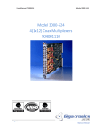
Figure 1-1. Series 373XXA Vector Network Analyzer System
Chapter 1
General Information
1-1
SCOPE OF MANUAL
This manual provides general service and preventive maintenance information for the ANRITSU 373XXA family of Vector Network
Analyzer (VNA) systems. It contains procedures for:
q
Testing the instrument for proper operation.
q
Verifying measurement accuracy and traceability to National Institute of Standards and Technology (NIST).
q
Troubleshooting a failed instrument to the exchange subassembly level or the subsystem requiring adjustment.
q
Adjusting instrument internal sub-systems.
q
Locating and replacing failed parts.
Throughout this manual, the terms “373XXA” and “373XXA VNA”
will be used interchangeably to refer to all Series 37300A Network
Analyzer system models, unless otherwise noted.
1-2
1-3
1-4
INTRODUCTION
This chapter of the manual provides a general description of 373XXA
VNA systems, system serial numbers, frequency ranges, and related
manuals. Also included is information about the level of maintenance covered in this manual, service strategy, available service facilities, and
static-sensitive component handling precautions. A list of recommended
test equipment is also provided.
IDENTIFICATION
NUMBER
All ANRITSU instruments are assigned a six-digit ID number, such as
“401001”. This number appears on a decal affixed to the rear panel.
Please use this identification number during any correspondence with
ANRITSU Customer Service about this instrument.
ONLINE MANUAL
This manual is available on CD ROM as an Adobe Acrobat™ (*.pdf)
file. The file can be viewed using Acrobat Reader™, a free program
that is also available on the CD ROM. This file is “linked” such that
the viewer can choose a topic to view from the displayed “bookmark”
list and “jump” to the manual page on which the topic resides. The
text can also be word-searched. Contact ANRITSU Customer Service
for price and availability.
373XXA MM
1-3
SYSTEM DESCRIPTION
1-5
SYSTEM DESCRIPTION
373XXA Model Frequencies
Model
Freq Range
37317A
22.5 MHz to 8.6 GHz
37325A
40.0 MHz to 13.5 GHz
37347A
40.0 MHz to 20.0 GHz
37369A
40.0 MHz to 40.0 GHz
37397A
40.0 MHz to 65.0 GHz
1-6
RELATED MANUALS
GENERAL INFORMATION
The 373XXA Analyzers are microprocessor controlled Vector Network
Analyzers. Each is a single-instrument system that contains a built-in
signal source, a test set, and an analyzer subsystem. A typical model
(37369A) is shown in Figure 1-1. These analyzers are produced in five
models that cover a range of from 22.5 MHz to 65 GHz. The table at left
lists the frequencies for each model.
The 373XXA Vector Network Analyzer Operation Manual (10410-00183)
describes the front panel operation for all 373XXA models. It also contains general information, specifications, and Performance Verification
procedures for all models.
The 37XXX Series Vector Network Analyzer Programming Manual
(10410-00200) describes all 373XXA GPIB commands and provides
programming information for operation of the 373XXA remotely via
the IEEE-488 General Purpose Interface Bus. Included at the rear of
this manual is the 37XXX Series Vector Network Analyzer GPIB
Quick Reference Guide (10410-00201).
Model 360X/373XXA VNA Performance Verification Software Users
Guide, P/N: 10410-00208 (located in Appendix E at the rear of this
manual). This Software Users Guide explains in detail the procedures
to be used for the installation and operation of the 373XXA VNA Verification Software on your computer/controller.
1-7
STANDARD OPTIONS
The standard 373XXA VNA options and their respective Upgrade Kit part
numbers are:
Option*
Description
Upgrade Kit
Opt 1
Rack Mount with slides
ND39486
Opt 1A
Rack Mount
ND40916
Opt 2A
Time Domain (Microwave
Units)
ND39477
Opt 2B
Time Domain (RF Units)
ND40914
Opt 10A
High Stability Ovenized Time
Base
ND45045
∗ All options listed can be installed at ANRITSU Service Centers
1-4
373XXA MM
GENERAL INFORMATION
1-8
SERVICE STRATEGY
SERVICE STRATEGY
This paragraph provides an overview of the 373XXA VNA service strategy and available service facilities. It also provides references to the information in various locations in this manual needed to accomplish the service functions required for the 373XXA VNA.
Appendices - Refer to the Appendices at the rear of this manual for detailed descriptions of the following:
Functional Assembly
Level Troubleshooting
q
Diagnostics Menus and GPIB Commands.
q
Error Messages.
q
System Block Diagrams.
q
Parts Locator Diagrams.
The 373XXA modular design, extensive built-in diagnostics, and automated service tools are designed to support fast exchange of functional assembly level repairs.
Failed assemblies are not field repairable. Once an assembly is found
to be faulty, it should be returned to an authorized ANRITSU Service
Center for exchange. Refer to the description of the Exchange Assembly Program in Chapter 2, Replaceable Parts.
The procedures for troubleshooting a failed 373XXA VNA are described in this manual in Chapter 5, Troubleshooting.
Internal Hardware
Adjustments and
Calibrations
There are five automated internal hardware field calibrations. Two of
them are used to characterize the 373XXA frequency and power generation sub-systems. These calibrations insure fast, consistent phase lock of
system frequencies and proper compensation, leveling, and flatness of
system power at the front panel test ports.
To conduct these calibrations, you need only connect the appropriate
test equipment (counter or power meter) to the 373XXA and initiate
the calibration. The 373XXA will control itself and the externally connected test equipment to perform measurements and store calibration
constants in its internal battery backed RAM (BBRAM).
The procedures for adjusting the 373XXA VNA are described in this
manual in Chapter 6, Adjustments.
Internal Service Log
The 373XXA continuously monitors itself for proper operation. Should a
failure occur, it notifies the user via a failure message on the display
screen. (In remote-only operation, it also sets the GPIB Status Byte, if
enabled.) It also writes the error message along with some data pertinent
to the failure to an internal service log stored in battery backed memory.
The service log can be checked at any time to view (without erasing)
all error messages that were written into it. It is capable of storing
373XXA MM
1-5
SERVICE SUPPORT
GENERAL INFORMATION
more than 30 pages of service messages and data. The 373XXA will
automatically remove the oldest errors first to make room for new errors, if necessary. To check the contents of the service log, use the procedure described in Chapter 3, Operational Tests.
NOTE
A printed or disk file copy of the Service Log (with the failure in question) must be made available to ANRITSU
when exchanging a failed assembly, or when requesting
service support. Refer to Chapter 2, Replaceable Parts, for
further information.
System
Test/Certification
Quick operational checkout of the system may be accomplished by the
system user or for incoming inspection purposes using the “Operational
Checkout” chapter in the 373XXA Operations Manual. Those procedures
are useful in quickly verifying that the instrument’s primary measurement functions are operational and stable.
Full operational testing of the system is detailed in Chapter 3, Operational Tests. These tests should be performed annually, or more often
depending on system use.
Verification of the system’s measurement accuracy and other key performance parameters may be done using the procedures in Chapter 4,
Performance Verification. This should be performed annually, or more
often depending on system use.
Preventive Service
The 373XXA A9 Processor PCB contains a battery backed memory/real
time clock chip (BBRAM) and a static memory (SRAM) backup battery.
These have a finite life span and should be replaced periodically per the
procedures in Chapter 8, Removal and Replacement Procedures.
The BBRAM chip has a rated life span of 4 years. The SRAM backup
battery has a worst case elapsed time for SRAM battery protection of
200 days. The SRAM battery life span will vary according to how the
system is used; that is, how often the system is powered off for extended periods of time.
Servicing Specially
Modified Instruments
Instruments with customer requested special modifications performed by
ANRITSU will have an identifying Specials Modification number printed
on the rear panel. This number will be preceded with the letters SM, i.e.,
SM1234 is special modification number 1234.
Special instruments may have service requirements different from
those specified in this manual. Contact your local Service Center if you
need more information when servicing such instruments.
1-9
1-6
SERVICE SUPPORT
The following paragraphs briefly describe the various service support
services and aids available to you to help you maintain your 373XXA.
373XXA MM
GENERAL INFORMATION
Technical Support
SERVICE SUPPORT
Technical service support is available by contacting any ANRITSU
Worldwide Service Center (refer to paragraph 1-11). Or, service support
may be obtained directly from the factory by contacting:
ANRITSU Company
ATTN: Customer Service
490 Jarvis Drive
Morgan Hill, CA 95037-2809
Telephone: (408)-778-2000
FAX: (408)-778-0239
If servicing or repairing your own system and you need technical support, you will need to FAX or mail a printout of the items listed below
to the ANRITSU Customer Support Engineer:
q
q
q
q
Field Service Kits
Measurement data in question
“Operational Tests” results
System state (from UTILITY menu)
Service Log (from DIAGNOSTICS menu)
The field service kit listed below is available through your local ANRITSU
Sales or Service Center:
ND37200A-2, Field Service Kit
This kit provides for automated field test and performance verification
of the 373XXA. It is packaged in a hardened rolling case that also has
space for two, user supplied, verification and calibration kits and other
accessories.
The ND37200A-2, Field Service Kit is comprised of all major subassemblies of all models 40 Ghz and below high-end frequency.
ND53269, Field Service Kit
This kit provides for automated field test and performance verification
of the 373XXA 50 and 65 GHz models (37397A). It supplements kit
ND37200A-2.
Service Software
The service software listed below is contained on the diskette located at
the rear of this manual:
ANRITSU 37XXX Test Software (2300-178).
This software contains a series of automated tests designed to insure
the 373XXA signal paths are functioning properly and capable of supporting stable calibrations and measurements. See Operational Tests
Chapter for details.
ANRITSU 37XXX Performance Verification Software (2300-237).
This software is used to verify the 373XXA published measurement accuracy and traceability to the U.S. National Institute of Standards and
Technology (NIST). See Chapter 4, Performance Verification, for details.
373XXA MM
1-7
SERVICE SUPPORT
Verification Kits
GENERAL INFORMATION
The ANRITSU Verification Kits listed below are used in conjunction with
the 37XXX Performance Verification Software (above). See Chapter 4, Performance Verification, for further information.
N Verification Kit (Model 3663)
Contains precision N Connector components with characteristics that
are traceable to the NIST.
Use for Models 37317A and below with Option 7N and 7 NF.
3.5 mm Verification Kit (Model 3666)
Contains precision 3.5 mm Connector components with characteristics
that are traceable to the NIST.
Use for Models 37347A and below with Option 7A.
GPC-7 Verification Kit (Model 3667)
Contains precision GPC-7 Connector components with characteristics
that are traceable to the NIST.
Use for Models 37317A and below with Option 7A.
K Verification Kit (Model 3668)
Contains precision K Connector components that are traceable to the
NIST.
V Verification Kit (Model 3669B)
Contains precision V Connector components that are traceable to the
NIST.
Test Fixtures/ Aids
The test fixtures and test aids listed below are available through your local ANRITSU Sales or Service Center:
Rear Panel Printer Port Test Fixture (B39553).
This test fixture is used to check out digital printer interface circuits
on the rear panel assembly.
GPIB Cable (2100-2).
This cable is used to check out digital GPIB interface circuits on the
rear panel assembly.
Failed Assembly
Exchange Program
The exchange program allows a customer to quickly exchange a failed
subassembly for a factory refurbished, fully system-tested and unit that is
under warranty. This results in significant time and price savings as compared with ordering a new assembly.
Refer to Chapter 2, Replaceable Parts, for a complete list of exchangeable assemblies for all Series 373XXA models.
NOTE
When sending a failed assembly to the factory for exchange, a copy of the Service Log must always accompany the failed assembly. Refer to Chapter 2, Replaceable
Parts, for further information.
1-8
373XXA MM
GENERAL INFORMATION
1-10
1-11
1-12
1-13
PERFORMANCE SPECIFICATIONS
PERFORMANCE
SPECIFICATIONS
The performance specifications for all Series 373XXA models are contained in the Technical Data Sheets that are located in Appendix D,
Performance Specifications.
SERVICE CENTERS
ANRITSU Company offers a full range of repair and calibration services
at fully staffed and equipped service centers throughout the world. Table
2-1, located on page 2-4, lists all ANRITSU services centers.
STATIC SENSITIVE
COMPONENT
HANDLING
PROCEDURES
The 373XXA contains components that can be damaged by static electricity. Figure 1-2 illustrates the precautions that should be followed when
handling static-sensitive subassemblies and components. If followed,
these precautions will minimize the possibilities of static-shock damage to
these items.
RECOMMENDED TEST
EQUIPMENT
Table 1-1 lists the recommended test equipment to be used for all maintenance activities for all Series 373XXA models. Note the “Use” codes
listed in the right hand column of the table. These codes list the applicable maintenance activities for the equipment listed.
373XXA MM
1-9
RECOMMENDED TEST EQUIPMENT
GENERAL INFORMATION
Table 1-1. Recommended Test Equipment (1 of 2)
INSTRUMENT
Computer/Controller
CRITICAL
SPECIFICATION
PC with Windows 95 or later and National Instruments GPIB hardware and software.
Test Software
Floppy Disk
Formatted, IBM PC format
GPIB Cable
RECOMMENDED
MANUFACTURER/MODEL
Any
USE*
*
O, P
ANRITSU 2300-178
O
DS/HD 1.44 Mbyte
A
ANRITSU 2100-2, or equivalent
O, P,
A
RF/Microwave Cable
DC – 40 GHz, K type connectors (male
or female), Length, 3 ft.
Any
P, A
BNC Cable
Length, 4 ft., 2 each
Any
O
ANRITSU B39553
O
Printer Port Test
Fixture
Thru Line
For models 37317A and below
For models 37325A and above:
ANRITSU 3670A50-2, 3671A50-2
ANRITSU 3670K50-2, 3671K50-2
O, P
Calibration Kit
For models 37317A and below, with Opt 7A:
For models 37317A and below, with Opt 7N or
7NF:
For models 37325A and above:
For models 37325A and below, with Opt 7S:
For model 37397A
ANRITSU 3651-1*
ANRITSU 3653
O, P
Performance Verification Software
Connector Verification
Kit
∗
ANRITSU 3652-1*
ANRITSU 3650-1*
ANRITSU 3654B
ANRITSU 2300-237
P
For models 37217B and below w/Opt 7A:
For models 37217B and below, with Opt 7N or
7NF:
For models 37225B and above:
For models 37247B and below, with Opt 7S:
ANRITSU 3667
P
For model 37397A
ANRITSU 3669B
ANRITSU 3663
ANRITSU 3668
ANRITSU 3666
Calibration Kit sliding load (Option {-1}), required for Performance Verification only.
∗∗ USE CODES:
A Adjustment / Internal Hardware Calibration
O Operational Testing
P Performance Verification
T Troubleshooting
1-10
373XXA MM
GENERAL INFORMATION
RECOMMENDED TEST EQUIPMENT
Table 1-1. Recommended Test Equipment (2 of 2)
INSTRUMENT
CRITICAL
SPECIFICATION
RECOMMENDED
MANUFACTURER/MODEL
USE*
*
Assurance Air Line
For models 37317A and below w/Opt 7A:
For models 37317A and below w/Opt 7N:
For models 37317A and below w/Opt 7NF:
For models 37317A and above:
For models 37317A and below w/Opt 7S:
ANRITSU 18A50
ANRITSU 18NF50
ANRITSU 18N50
ANRITSU T1519
ANRITSU T1147-2
P
Offset Termination
For models 37317A and below w/Opt 7A, 7N,
7NF:
All other models
ANRITSU 29A50-20
P
Frequency Counter
Frequency: 0.1 to 26.5 GHz
Input Impedance: 50Ω
EIP Microwave, Inc., Model 578B
Digital Multimeter
Resolution: 4 12 digits
DC Accuracy: 0.1 %
AC Accuracy: 0.1 %
Any
T
Oscilloscope
Bandwidth: DC to 100 MHz
Sensitivity: 2 mV
Horiz. Sensitivity: 50 ns/division
Tektronix, Inc.
Model 2445
T
Power Meter 1, with:
Power Range: –30 to +20 dBm
(1 mW to 100 mW)
Other: GPIB controllable
HP 437B with Option 22 (GPIB)
P, A
Power Sensor 1
or:
Frequency Range: 0.05 to 50 GHz
Power Range: –70 to +47 dBm
(100 pW to 50 W)
Other: GPIB controllable
Frequency Range: 0.01 to 40 GHz
HP 8487A
P, A
Power Meter 2, with:
Power Sensor 2
Power Meter and Power
Sensor
Gauging Set
Frequency Range: to 65 GHz
GPC-7 Gauging Set
K Connector Gauging Set
ANRITSU 29KF50-15
P, A
Gigatronics 8541 or 8542
Gigatronics 80304A
Anritsu Model ML24xxA Power Meter
and MA2474A (40 GHz and below)
and Model SC6230 (to 65 GHz)
Power Sensors
ANRITSU 01-161
ANRITSU 01-162
P, A
O, T
∗∗ USE CODES:
A Adjustment / Internal Hardware Calibration
O Operational Testing
P Performance Verification
T Troubleshooting
373XXA MM
1-11
STATIC HANDLING
GENERAL INFORMATION
1.
Do not touch exposed contacts on
any static sensitive component.
2.
4.
Wear a static-discharge wristband
when working with static sensitive
components.
5.
7.
Handle PCBs only by their edges. 8.
Do not handle by the edge connectors.
Do not slide static sensitive compo- 3.
nent across any surface.
Do not handle static sensitive components in areas where the floor or
work surface covering is capable of
generating a static charge.
Label all static sensitive devices.
6.
Keep component leads shorted together whenever possible.
Lift & handle solid state devices by
their bodies – never by their leads.
9.
Transport and store PCBs and
other static sensitive devices in
static-shielded containers.
10.
ADDITIONAL PRECAUTIONS:
Keep workspaces clean and free of any objects capable of holding or storing a static charge.
•
Connect soldering tools to an earth ground.
•
Use only special anti-static suction or wick-type desoldering tools.
•
Figure 1-2. Static Sensitive Component Handling Procedures
1-12
373XXA MM
Chapter 2
Replaceable Parts
Table of Contents
2-1
INTRODUCTION · · · · · · · · · · · · · · · · · · · · · · · · · 2-3
2-2
EXCHANGE ASSEMBLY PROGRAM · · · · · · · · · · · · · · 2-3
2-3
REPLACEABLE SUBASSEMBLIES AND PARTS · · · · · · · 2-3
2-4
PARTS ORDERING INFORMATION · · · · · · · · · · · · · · 2-4
Chapter 2
Replaceable Parts
2-1
2-2
INTRODUCTION
This chapter provides replaceable parts information for all 373XXA
models. The major replaceable 373XXA assemblies and parts are listed
in Tables 2-2 through 2-8. The locations of these assemblies/parts are
shown in Figures 2-1 through 2-4.
EXCHANGE ASSEMBLY
PROGRAM
ANRITSU maintains a module exchange program for selected subassemblies. If a malfunction occurs in one of these subassemblies, the defective
item can be exchanged. Upon receiving your request, ANRITSU will ship
the exchange subassembly to you, typically within 24 hours. You then
have 45 days in which to return the defective item. All exchange subassemblies or RF assemblies are warranted for 90 days from the date of
shipment, or for the balance of the original equipment warranty, whichever is longer.
NOTE
When sending a failed assembly to the factory for exchange, a copy of the Service Log must always accompany the failed assembly. This copy may be a printout, or a
saved disk copy. Due to the importance of the service log
information to the ANRITSU factory Service Engineers,
the exchange prices are only valid if the service log data is
included with the failed assembly.
Please have the exact model number and serial number of your unit
available when requesting this service, as the information about your
unit is filed according to the instrument’s model and serial number.
For more information about the program, contact your local sales representative or call ANRITSU Customer Service direct (refer to paragraph 2-4.
2-3
REPLACEABLE
SUBASSEMBLIES AND
PARTS
Tables 2-2 through 2-5, (starting page 2-5) list the major replaceable subassemblies and parts for the 373XXA. These assemblies/parts are presently covered by the ANRITSU exchange assembly program. Table 2-6
(page 2-6) lists disposable parts for the 373XXA, and Table 2-7 and 2-8
lists factory-repairable parts for the 373XXA. (The parts listed in Tables
2-6 through 2-8 are not presently on the exchange assembly program.)
NOTE
The 373XXA A17 Motherboard PCB Assembly is not a
field-replaceable item.
373XXA MM
2-3
PARTS ORDERING INFORMATION
2-4
PARTS ORDERING
INFORMATION
REPLACEABLE PARTS
All parts listed in Tables 2-2 through 2- 8 may be ordered from your local
ANRITSU service center (Table 2-1). Or, they may be ordered directly
from the factory at the following address:
ANRITSU Company
ATTN: Customer Service
490 Jarvis Drive
Morgan Hill, CA 95037-2809
Telephone: (408)-778-2000
FAX: (408)-778-0239
Table 2-1. ANRITSU Service Centers
UNITED STATES
ANRITSU COMPANY
490 Jarvis Drive
Morgan Hill, CA 95037-2809
Telephone: (408) 778-2000
FAX: (408) 778-0239
ANRITSU ANRITSU COMPANY
685 Jarvis Drive
Morgan Hill, CA 95037-2809
Telephone: (408) 776-8300
FAX: (408) 776-1744
ANRITSU ANRITSU COMPANY
10 Kingsbridge Road
Fairfield, NJ 07004
Telephone: (201) 227-8999
FAX: (201) 575-0092
AUSTRALIA
ANRITSU PTY. LTD.
Level 2, 410 Church Street
North Parramatta
NSW 2151 Australia
Telephone: 026-30-81-66
Fax: 026-83-68-84
BRAZIL
ANRITSU ANRITSU ELECTRONICA
LTDA.
Praia de Botafogo, 440-SL 2401-Botafogo
2225-Rio de Janeiro-RJ-Brasil
Telephone: 021-28-69-141
Fax: 021-53-71-456
1800 Onna Atsugi-shi
Kanagawa-Prf. 243 Japan
Telephone: 0462-23-1111
FAX: 0462-25-8379
FRANCE
ANRITSU CORPORATION
#2103 Korea World Trade Center
159-1 Samsung-Dong
Kangnam-ku, Seoul
Telephone: (02) 551-2250
FAX: (02) 551-4941
ANRITSU ANRITSU S.A
9 Avenue du Quebec
Zone de Courtaboeuf
91951 Les Ulis Cedex
Telephone: 016-44-66-546
FAX: 016-44-61-065
GERMANY
ANRITSU ANRITSU GmbH
Rudolf Diesel Strabe 17
8031 Gilching
Telephone: 08-10-58-055
FAX: 08-10-51-700
INDIA
MEERA AGENCIES (P) LTD.
A-23 Hauz Khas
New Delhi 110 016
Telephone: 011-685-3959
FAX: 011-686-6720
ISRAEL
TECH-CENT, LTD
Haarad St. No. 7, Ramat Haahayal
Tel-Aviv 69701
Telephone: (03) 64-78-563
FAX: (03) 64-78-334
CANADA
ITALY
ANRITSU ANRITSU INSTRUMENTS LTD.
215 Stafford Road, Unit 102
Nepean, Ontario K2H 9C1
Telephone: (613) 828-4090
FAX: (613) 828-5400
ANRITSU ANRITSU Sp.A
Roma Office
Via E. Vittorini, 129
00144 Roma EUR
Telephone: (06) 50-22-666
FAX: (06) 50-22-4252
CHINA
ANRITSU BEIJING SERVICE
CENTER
2-4
416W Beijing Fortune Building
5 Dong San Huan Bei Lu
Chao Yang Qu, Beijing 100004, China
Telephone: 86-1-50-17-559
FAX: 86-1-50-17-558
JAPAN
KOREA
SINGAPORE
ANRITSU ANRITSU (SINGAPORE) PTE
LTD
3 Shenton Way #24-03
Shenton House
Singapore 0106
Telephone: 011-65-2265206
FAX: 011-65-2265207
SWEDEN
ANRITSU ANRITSU AB
Box 247
S-127 25 Skarholmen
Telephone: (08) 74-05-840
FAX: (08) 71-09-960
TAIWAN
ANRITSU CO., LTD.
8F, No. 96, Section 3
Chien Kuo N. Road
Taipei, Taiwan, R.O.C.
Telephone: (02) 515-6050
FAX: (02) 509-5519
UNITED KINGDOM
ANRITSU ANRITSU LTD.
200 Capability Green
Luton, Bedfordshire
LU1 3LU, England
Telephone: 05-82-41-88-53
FAX: 05-82-31-303
ANRITSU CORPORATION
373XXA MM
REPLACEABLE PARTS
PARTS ORDERING INFORMATION
Table 2-2. Printed Circuit Board Assemblies
Reference
Designator
373XXA
Option
Assembly / Part
Part Number
A1
LO1
D46866-3
A1
LO1
D86866-4*
A2
LO2
D50725-3
A3
Test A IF
D38503-4
A4
Reference IF
D41794-3
A4
Reference IF
D41794-4*
A5
A/D
D38505-3
A6
Test B IF
D38503-5
A7
LO3
D38507-3
LO3
D38507-4
A8
Source Lock/ Separation Control
D47488-3
A8
Source Lock/ Separation Control
D49334-3*
A9
Main Processor
B38509
A13
I/O #1
D38513-3
A14
I/O #2
D38514-3
A15
Graphics Processor
D44281-3
A16
Hard Disk (w/ PCB)
D41041-3
A18
Rear Panel PCB
D44255-3
A19**
Front Panel Switch PCB
A20**
Front Panel Control PCB
A21A1
Source YIG/Bias Control (p/o Signal Source Module)
D48516-3
A21A1
Source YIG/Bias Control (p/o Signal Source Module)
D48512-3*
A21A2
Source Control (p/o Signal Source Module)
D41841-3
A21A2
Source Control (p/o Signal Source Module)
D48513-3*
A24
VME Bus Terminator
D38524-3
A7
Opt 10
See Table 2-5
∗ Required for 37397A
∗∗ Part of the Front Panel Assembly (refer to Table 2-5).
373XXA MM
2-5
PARTS ORDERING INFORMATION
REPLACEABLE PARTS
Table 2-3. Test Set Assembly RF/Microwave Components, 37317A, 37325A, 37347A, 37369A
Assembly / Part
373XXA Model / Option
Part Number
Transfer Switch
All
D28580-1
46535*
Step Attenuator, 70 dB
All
4612K
Low Frequency Bridge w/ Bias Tee
37311A, 37317A
D28985
Coupler w/ Bias Tee
37325A and higher
D28967
40 GHz Quad Buffer Amp/Power Amplifier
37369A only
ND47533
Switched Doubler Module (SDM)
37369A only
D28685
All
Port 2 Step Attenuator
4612K
6 dB Pad
37369A only
43KC-10
20 dB Pad
37347A and below
43KC-20
20 GHz Quad Buffer Amp/Power Amplifier
All except 37369A
ND47532
* Used on serial numbers 975004, 975101, 975103, 980102, 980104, 980201, 980302, 980402, 980403, 980405,
980406, 980407, 980602, 980603, 980701, and above.
Table 2-4. Test Set Assembly RF/Microwave Components, 37397A
Assembly / Part
Part Number
Pinswitch
29855
Switched Doubler Module (SDM)
47520
Quadrupler (SQM)
48998
37GHz High Pass Filter
49247
Mux Coupler (Port 1)
49470
Mux Coupler (Port 2)
49480
Shaped Pad
52956
Bias Tee
53409
16.8 GHz Lowpass Filter
B28912
Access Loops (Front and Rear Panel)
B35569-195
Transfer Switch
D27030
3 dB Fixed Attenuator
ND26178
Step Attenuator
ND52564
Coupler
ND52929
Quad Buffer Amplifier/Power Amplifier
ND53249
2-6
373XXA MM
REPLACEABLE PARTS
PARTS ORDERING INFORMATION
Table 2-5. Miscellaneous /Integrated Assemblies
Assembly / Part
10 MHz Ovenized Oscillator
373XXA Model / Option
Part Number
Opt 10 only
ND39476
Power Supply Module
All
40-116
VGA Monitor
All
2000-322
Floppy Disk Assy
All
C38550
Front Panel Assy (w/ Front Panel, A19 and A20 PCB’s, and all Model
All
ND42700
All
B38533
ID Overlays)
Fan Assembly, Rear Panel
Front Panel Assy (incudes front panel, A19 and A20 PCBs, and all
model ID overlays)
LCD Equipped
ND44606
Power Supply
LCD Equipped
40-114
Liquid Crystal Display (LCD)
LCD Equipped
15-88
Liquid Crystal Display (LCD)
LCD Equipped
SN:972701 and above
15-92
Liquid Crystal Display (LCD)
LCD Equipped
SN:994600 and above
15-100
Table 2-6. Consummsable Parts
Assembly / Part
373XXA Model / Option
Part Number
System Software
All
2300-212
Front Panel Encoder Knob
All
2000-577
Front Panel Amber Lens
All
790-412
Fuse, 8A, Fast Blow 3AG Cartridge type (F1 Line fuse for power
supply assembly)
All
631-72
Battery Backed RAM
All
54-1350
Back-Up Battery
All
633-20
LCD Back Light Driver PCB
LCD Equipped
2000-770
LCD Back Light Lamp
LCD Equipped
632-55
373XXA MM
2-7
PARTS ORDERING INFORMATION
REPLACEABLE PARTS
Table 2-7. Signal Source Module RF/Microwave Components
Assembly / Part
373XXA Model / Option
Part Number
YIG Oscillator (2 - 20 GHz)
All
C21620-1
Down Converter
All
D27532
Switched Filter
37317A and below
D45243
Switched Filter
37325A and above
D45244
Table 2-8. Factory Repairable Non-Exchange Parts
Assembly / Part
2-8
373XXA Model / Option
Part Number
Test Port Connector, K-Male
All
34UK50
Test Port Connector, GPC-7
Opt 7A only
34UA50
Test Port Connector, 3.5 mm
Opt 7S only
34US50
Test Port Connector, type N
Opt 7N only
34UN50
Test Port Connector, type NF
Opt 7NF only
34UNF50
Test Port Connector, V
37397A
34YV50
373XXA MM
REPLACEABLE PARTS
PARTS ORDERING INFORMATION
Ovenized Reference Oscillator
(Option 10 only)
Power
Supply
Module
Printed Circuit
Board Assemblies,
A13-A16
Fan Assembly
Printed Circuit Board
Assemblies, A1-A9
VGA Monitor
Assembly
Signal
Source
Module
Front Panel Assembly
(Includes Front Panel PCB)
Figure 2-1. Major Assemblies Location Diagram (Top
373XXA MM
3
4
View)
2-9
PARTS ORDERING INFORMATION
Port 1
Coupler/Bridge*
Switched Doubler
Module**
REPLACEABLE PARTS
Port 2 Step
Attenuator
Port 2
Coupler/Bridge*
Floppy Disk Drive
Assembly
Step Attenuator
70dB
Transfer
Switch
A17 Motherboard
PCB Assembly
Power
Amplifier
A24 VME Bus
Terminator
PCB Assembly
20/40 GHz
Quad Buffer
Amp/Sampler*
* Refer to Table 2-3
** Model 37369A Only
10dB/20dB Pads*
A18 Rear Panel
PCB Assembly
Figure 2-2. Major Assemblies Location Diagram (Bottom View) (Not 37397A)
2-10
373XXA MM
REPLACEABLE PARTS
PARTS ORDERING INFORMATION
Port 1 Coupler
Port 2 Step Attenuator
Port 2 Coupler
Port 2 Bias Tee
Port 1 Bias Tee
Floppy Disk Drive Assy
Switched Doubler Module
Port 1 Step Attenuator
Port 2 37 GHz Hipass Filter
Port 1 MUX Coupler
Port 2 SQM
Port 2 MUX Coupler
Transfer Switch
SPDT Switch
A17 PCB
Port 1 37 GHz Hipass Filter
Power Amplifier
Port 1 SQM
Sampler/Buffer Amplifier
Shaped Pads
A24 PCB
A18 Rear Panel PCB
Figure 2-3. Major Assemblies Location Diagram (Bottom View) (37397A)
373XXA MM
2-11
PARTS ORDERING INFORMATION
REPLACEABLE PARTS
Figure 2-4. Signal Source Parts Location Diagram
2-12
373XXA MM
Chapter 3
Operational Tests
Table of Contents
3-1
INTRODUCTION · · · · · · · · · · · · · · · · · · · · · · · · · 3-3
3-2
CHECKING THE SERVICE LOG · · · · · · · · · · · · · · · · 3-4
3-3
SELF TEST · · · · · · · · · · · · · · · · · · · · · · · · · · · · 3-5
3-4
PERIPHERALS AND INTERFACES
LCD Test · · · · · · · · · · · · · · · ·
Front Panel Test · · · · · · · · · · · ·
External Keyboard Interface Test · · ·
Printer Interface Test · · · · · · · · ·
GPIB Interface Test · · · · · · · · · ·
3-5
SIGNAL PATH · · · · · · · · · · · · · · · · · · · · · · · · · · 3-10
·
·
·
·
·
·
·
·
·
·
·
·
·
·
·
·
·
·
·
·
·
·
·
·
·
·
·
·
·
·
·
·
·
·
·
·
·
·
·
·
·
·
·
·
·
·
·
·
·
·
·
·
·
·
·
·
·
·
·
·
·
·
·
·
·
·
·
·
·
·
·
·
·
·
·
·
·
·
·
·
·
·
·
·
3-6
3-6
3-7
3-7
3-7
3-9
Chapter 3
Operational Tests
3-1
INTRODUCTION
The tests in this section provide a means of fully testing the 373XXA VNA
system for proper operation and signal stability. These tests are intended
to be used as a periodic check of the operational functionality of the
373XXA.
The tests should be performed in their entirety at least once annually.
Although there is no requirement to do so, the tests should generally
be run in the sequence presented.
NOTE
The procedures presented in Chapter 4, Performance Verification, provide the means to test the accuracy of the tests
performed by the 373XXA.
Please ensure you have read and fully understand the servicing concepts for the 373XXA presented in Chapter 1 prior to continuing with
this chapter.
Operational Tests for the 373XXA consist of the following:
q
Checking the Service Log
q
Self Test
q
Peripherals and Interface Testing
q
Signal Path Tests (includes Checking the Service Log and Self
Test.)
These tests are described in paragraphs 3-2 through 3-5, which start
on the next page.
373XXA MM
3-3
CHECKING THE SERVICE LOG
3-2
CHECKING THE
SERVICE LOG
OPERATIONAL TESTS
Checking the service log consists of viewing the entries written into the
log.
CAUTION
The service log contains historical information about instrument condition and any failures that may have occurred. It should be cleared only by a qualified service
engineer. Such clearing shuld be accomplished only upon
determining that the errors need not be saved to disk, or
printed out for service purposes.
Procedure:
DIAGNOSTICS
OPTIONS
START SELF TEST
TRIGGERS
READ SERVICE LOG
REAR PANEL
OUTPUT
INSTALLED OPTIONS
DIAGNOSTICS
PERIPHERAL TESTS
MULTIPLE SOURCE
CONTROL
TROUBLESHOOTING
(FOR SERVICE
ONLY)
PRESS <ENTER> TO
SELECT
HW CALIBRATIONS
(FOR SERVICE
ONLY)
PRESS <ENTER>
TO SELECT
Step 1.
Press the Option Menu key (Enhancement key group) to display the OPTIONS menu.
Step 2.
Select DIAGNOSTICS from menu (left); then select
READ SERVICE LOG from the DIAGNOSTICS menu.
The 373XXA will now display the contents of the service
log. The display consists of a header and an error listing.
The header contains a variety of system service information. The error listing contains error messages for failures
that may have occurred during operation.
NOTE
• Errors 7201–7209, GPIB remote operation programming errors, report that one
or more external GPIB programming errors has been detected. These messages
do not indicate a 373XXA system fault.
• Informational messages 0000–0099 report
the pass/fail status of a peripheral access.
These messages do not indicate a 373XXA
system fault.
Any other error messages in the service log may indicate
an instrument problem and should be investigated. Refer
to the Chapter 5, Troubleshooting, for further information.
CAUTION
The CLEAR SERVICE LOG menu selection will immediately and permanently clear
all the error message entries from the service log. (However, it will not clear the
header information.) See Caution message
at top of page.
3-4
373XXA MM
OPERATIONAL TESTS
3-3
SELF TEST
SELF TEST
The self test performs a series of tests that verify that various internal
373XXA circuits are functional and operating properly.
To start the self test:
Step 1.
Press the Option Menu key (Enhancement key group) to display the OPTIONS menu.
Step 2.
Select DIAGNOSTICS from menu; then select START
SELF TEST (below).
OPTIONS
DIAGNOSTICS
TRIGGERS
START SELF TEST
REAR PANEL
OUTPUT
READ SERVICE LOG
DIAGNOSTICS
MULTIPLE SOURCE
CONTROL
PRESS <ENTER> TO
SELECT
INSTALLED OPTIONS
PERIPHERAL TESTS
TROUBLESHOOTING
(FOR SERVICE
ONLY)
HW CALIBRATIONS
(FOR SERVICE
ONLY)
PRESS <ENTER> TO
SELECT
Step 3.
Wait for test sequence to complete. (Once invoked, this test
requires no user interaction or external equipment.)
Upon completion, the net pass/fail result of the self test is shown on
the CRT display. If the 373XXA is in remote-only operation, the results are reported via the GPIB output buffer. If the self test fails, detailed error messages will be written into the service log.
If self test fails:
q Check the service log to view failure messages.
q Proceed to Chapter 5, Troubleshooting.
373XXA MM
3-5
PERIPHERALS AND INTERFACES
3-4
PERIPHERALS AND
INTERFACES
LCD Test
OPERATIONAL TESTS
These tests are used to verify the operation of the liquid-crystal display
(LCD), front panel keys, and peripheral devices that are used with the
373XXA. They consist of the following:
q
LCD Test
q
Front Panel Test
q
External Keyboard Interface Test
q
Printer Interface Test
q
GPIB Interface Test
This test verifies that the 373XXA LCD is functioning correctly.
NOTE
The External VGA Out Connector can also be tested when
using this procedure if an external VGA monitor is connected.
Procedure:
Step 1.
Press the Option Menu key (Enhancement key group) to display the OPTIONS menu.
Step 2.
Select DIAGNOSTICS from menu; then in sequence select: PERIPHERAL TESTS, and then CRT DISPLAY.
See diagram below.
OPTIONS
PERIPHERAL TESTS
DIAGNOSTICS
TRIGGERS
START SELF TEST
CRT DISPLAY
REAR PANEL
OUTPUT
READ SERVICE LOG
FRONT PANEL
INSTALLED OPTIONS
EXTERNAL KEYBOARD
DIAGNOSTICS
MULTIPLE SOURCE
CONTROL
PRESS <ENTER> TO
SELECT
PERIPHERAL TESTS
TROUBLESHOOTING
(FOR SERVICE
ONLY)
PRINTER INTERFACE
GPIB INTERFACE
PREVIOUS MENU
HW CALIBRATIONS
(FOR SERVICE
ONLY)
PRESS <ENTER> TO
SELECT
PRESS <ENTER> TO
SELECT
Step 3.
Follow instructions on the CRT screen until test is completed.
If test fails, proceed to Chapter 5, Troubleshooting.
3-6
373XXA MM
OPERATIONAL TESTS
Front Panel Test
PERIPHERALS AND INTERFACES
This test verifies that the control keys in each of the 373XXA key groups
are functioning correctly.
Procedure:
Step 1.
Press the Option Menu key (Enhancement key group) to display the OPTIONS menu.
Step 2.
Select DIAGNOSTICS from menu; then in sequence select: PERIPHERAL TESTS, and then FRONT PANEL.
See diagram below.
OPTIONS
DIAGNOSTICS
PERIPHERAL TESTS
TRIGGERS
START SELF TEST
CRT DISPLAY
REAR PANEL
OUTPUT
READ SERVICE LOG
FRONT PANEL
INSTALLED OPTIONS
EXTERNAL KEYBOARD
DIAGNOSTICS
MULTIPLE SOURCE
CONTROL
PRESS <ENTER> TO
SELECT
PERIPHERAL TESTS
TROUBLESHOOTING
(FOR SERVICE
ONLY)
HW CALIBRATIONS
(FOR SERVICE
ONLY)
PRINTER INTERFACE
GPIB INTERFACE
PREVIOUS MENU
PRESS <ENTER> TO
SELECT
PRESS <ENTER> TO
SELECT
Step 3.
Follow instructions on the screen until test is completed.
If test fails, proceed to Chapter 5, Troubleshooting.
External Keyboard
Interface Test
This test verifies that the 373XXA external keyboard interface is functioning correctly.
Equipment Required:
An IBM compatible keyboard is required for this test.
Procedure:
Step 1.
Press the Option Menu key (Enhancement key group) to display the OPTIONS menu.
Step 2.
Select DIAGNOSTICS from menu; then in sequence select: PERIPHERAL TESTS, and then EXTERNAL KEYBOARD. See diagram above.
Step 3.
Follow instructions on the screen until test is completed.
If test fails, proceed to Chapter 5, Troubleshooting.
Printer Interface Test
373XXA MM
This test verifies that the 373XXA printer interface is functioning correctly.
3-7
PERIPHERALS AND INTERFACES
OPERATIONAL TESTS
Equipment Required:
Printer Test Fixture (ANRITSU PN: B39553)
Procedure:
Step 1.
Press the Option Menu key (Enhancement key group) to display the OPTIONS menu.
Step 2.
Select DIAGNOSTICS from menu; then in sequence select: PERIPHERAL TESTS, and then PRINTER INTERFACE. See diagram below.
OPTIONS
DIAGNOSTICS
PERIPHERAL TESTS
TRIGGERS
START SELF TEST
CRT DISPLAY
REAR PANEL
OUTPUT
READ SERVICE LOG
FRONT PANEL
INSTALLED OPTIONS
EXTERNAL KEYBOARD
DIAGNOSTICS
MULTIPLE SOURCE
CONTROL
PRESS <ENTER> TO
SELECT
PERIPHERAL TESTS
TROUBLESHOOTING
(FOR SERVICE
ONLY)
HW CALIBRATIONS
(FOR SERVICE
ONLY)
PRINTER INTERFACE
GPIB INTERFACE
PREVIOUS MENU
PRESS <ENTER> TO
SELECT
PRESS <ENTER> TO
SELECT
Step 3.
Follow instructions on the screen until test is completed.
If test fails, proceed to Chapter 5, Troubleshooting.
3-8
373XXA MM
OPERATIONAL TESTS
GPIB Interface Test
PERIPHERALS AND INTERFACES
This test verifies that the 373XXA printer interface is functioning correctly.
Equipment Required:
GPIB cable (ANRITSU PN: 2100-2), or equivalent
CAUTION
Insure that no other cables are connected to either of the
two rear panel GPIB ports when performing this test.
Procedure:
Step 1.
Press the Option Menu key (Enhancement key group) to display the OPTIONS menu.
Step 2.
Select DIAGNOSTICS from menu; then in sequence select: PERIPHERAL TESTS, and then GPIB INTERFACE. See diagram below.
OPTIONS
PERIPHERAL TESTS
DIAGNOSTICS
TRIGGERS
START SELF TEST
CRT DISPLAY
REAR PANEL
OUTPUT
READ SERVICE LOG
FRONT PANEL
INSTALLED OPTIONS
EXTERNAL KEYBOARD
DIAGNOSTICS
MULTIPLE SOURCE
CONTROL
PRESS <ENTER> TO
SELECT
PERIPHERAL TESTS
TROUBLESHOOTING
(FOR SERVICE
ONLY)
PRINTER INTERFACE
GPIB INTERFACE
PREVIOUS MENU
HW CALIBRATIONS
(FOR SERVICE
ONLY)
PRESS <ENTER> TO
SELECT
PRESS <ENTER> TO
SELECT
Step 3.
Follow instructions on the screen until test is completed.
If test fails, proceed to Chapter 5, Troubleshooting.
373XXA MM
3-9
SIGNAL PATH
3-5
SIGNAL PATH
OPERATIONAL TESTS
These are a series of automated tests designed to insure the 373XXA internal signal paths are functioning properly and are capable of supporting stable calibrations and measurements. These test are performed using a software test program and an external computer/controller.
The test software performs the following operations and tests:
q
Service Log Check
q
Self Test
q
Basic Sweep Operation and Speed Test
q
High Level Noise Test
q
System Stability Test
q
RF Power Generation and Control Test
q
Step Attenuators Accuracy and Repeatability Test
q
Video IF Bandwidth Filters Operation Test
q
Sampler Efficiency and Stability Test
q
LO1/LO2 Linearity Test
q
Source FM/Lock Signal Linearity Test
Equipment required:
37XXX Test Software (ANRITSU PN: 2300-178)
External computer/controller; refer to Table 1-1 located on page 1-9.
GPIB cable (ANRITSU PN: 2100-2), or equivalent
Procedure:
Step 1.
Refer to file “Readme.txt” of the distribution disk for information regarding setup of the computer/controller.
Step 2.
Using the GPIB cable, connect the external computer/controller to the IEEE 488.2 GPIB Interface port on the
373XXA rear panel.
Step 3.
Program may be run from floppy disk or copied to any
folder in the computer and run from there.
Step 4.
Peform Non-Ratio and Transmission tests.
If any tests fail, refer to the Troubleshooting and Help selections of the
Test Software menu for assistance.
3-10
373XXA MM
Chapter 4
Performance Verification
Table of Contents
4-1
INTRODUCTION · · · · · · · · · · · · · · · · · · · · · · · · · 4-3
4-2
CALIBRATION AND MEASUREMENT CONDITIONS · · · · 4-3
Standard Conditions · · · · · · · · · · · · · · · · · · · · · · · · 4-3
Special Precautions: · · · · · · · · · · · · · · · · · · · · · · · · 4-4
4-3
MEASUREMENT ACCURACY · · · · · · · · · · · · · · · · · · 4-4
Verification Software · · · · · · · · · · · · · · · · · · · · · · · 4-4
Verification Result Determination · · · · · · · · · · · · · · · · 4-5
4-4
VERIFICATION PROCEDURE · · · · · · · · · · · · · · · · · · 4-5
4-5
KEY SYSTEM PARAMETERS · · · · · · · · · · · · · · · · · 4-6
Measurement Environment Considerations · · · · · · · · · · · 4-6
Measurement Technique · · · · · · · · · · · · · · · · · · · · · 4-7
373XXA MM
4-1
4-2
373XXA MM
Chapter 4
Performance Verification
4-1
INTRODUCTION
This chapter provides specific procedures to be used to verify that the
373XXA is making accurate, traceable S-parameter measurements. You
should perform the verification procedures in paragraph 4-3, “Verifying
Measurement Accuracy,” at least once annually.
Additionally, this chapter includes procedures that may be used to
measure the following key system performance parameters:
q
Effective Source Match
q
Effective Directivity
q
System Dynamic Range
q
Frequency Accuracy
q
Power Level Accuracy
The Operational Tests described in Chapter 3 should be performed
prior to verifying system performance.
Please ensure you have read and fully understand the servicing concepts for the 373XXA presented in Chapter 1 prior to continuing with
this chapter.
4-2
CALIBRATION AND
MEASUREMENT
CONDITIONS
Extremes in the surrounding environmental conditions and the condition
and stability of the test port connectors, through-cable, and calibration kit
determine system measurement integrity to a large extent.
These are all user controlled conditions, and as such, should be evaluated periodically for impact on system performance. If these conditions
vary significantly with time, the system verification procedures should
be performed more often than the recommended annual cycle.
Standard Conditions
The standard conditions specified below must be observed when performing any of the operations in this chapter — both during calibration and
during measurement.
Warm-up Time: One hour minimum.
Environmental Conditions:
Temperature: 23 +/- 3 deg C
Relative Humidity: 20-50% recommended.
373XXA MM
4-3
MEASUREMENT ACCURACY
PERFORMANCE VERIFICATION
Error Correction:
Perform software-guided 12 term calibration.
Special Precautions:
When performing the procedures in this chapter, observe the following
precautions:
q
q
q
q
4-3
MEASUREMENT
ACCURACY
Verification Software
Minimize vibration and movement of system and attached components and through-cable.
Clean and check pin depth and condition of all adapters,
through-cable(s), and calibration components.
Pre-shape the through-cable(s) so as to minimize its movement during calibration and measurement activities.
Ensure the system remains motion free in stable environmental
conditions as defined above throughout warm-up, calibration, and
measurement activities.
The verification procedures described in the following paragraphs verify
the published measurement accuracy and measurement traceability* for
the 373XXA.
These procedures use the ANRITSU VNA Verification Software, PN:
2300-237, and the NIST traceable impedance transfer standards contained in the appropriate ANRITSU Verification Kit. The Standard Conditions and Special Precautions described in paragraph 4-2 should be
observed when performing these procedures.
The appropriate ANRITSU Verification Kit to be used for performing
these procedures is model dependent, as follows:
q
q
q
Models 37317A and below, with Opt 7A: Verification Kit 3667
All Models using K Connector test ports: Verification Kit 3668
Models 37397A: Verification Kit 3669B
The impedance transfer standards contained in these kits are:
q
q
q
q
20 dB Attenuation Standard
50 dB Attenuation Standard
50 Ohm Air Line Standard
25 Ohm Mismatch (Beatty) Standard
The verification software performs the following functions:
q
q
q
q
It guides the user through a full 12 Term calibration of the 373XXA.
It guides the user through the measurement of the S-parameters of
the NIST traceable impedance transfer standards (below).
It verifies the measured values are within the specified measurement uncertainty limits.
It indicates the pass/fail status of the measurements on the CRT
display. It can also provide a hard copy printout of the measured
∗ Traceability to the U.S. National Institute of Standards and Technology (NIST)
4-4
373XXA MM
PERFORMANCE VERIFICATION
VERIFICATION PROCEDURE
data, measurement uncertainties, and the impedance transfer standards used.
NOTE
The total verification uncertainty in these
373XXA measurements includes the measurement uncertainty of the verification
standards and the 373XXA measurement
uncertainty.
Verification Result
Determination
The software verification process compares the measured S-parameter
data of the impedance transfer standards against the original standard
data for those devices that was obtained using the Factory Standard 360
Vector Network Analyzer System (at ANRITSU). The factory Standard
360 system is traceable to NIST through the ANRITSU Calibration Laboratory’s Impedance Standards. These standards are traceable to NIST
through precision mechanical measurements, NIST approved microwave
theory impedance derivation methods, and electrical impedance comparison measurements.
The quality of the verification results is very dependent on the degree
of care taken by the user in maintaining, calibrating, and using the
system. The most critical factors are:
q
q
q
The stability and quality of the devices in the calibration and verification kits.
The condition of 373XXA test port connectors and through-cables.
The pin depths of all connectors, and the proper torquing of connections. These same factors also affect 373XXA measurement quality.
Consult the Operating Manuals supplied with the ANRITSU Calibration and Verification Kits for proper use, care, and maintenance of the
devices contained in these kits.
4-4
VERIFICATION
PROCEDURE
The performance verification procedure for the ANRITSU 373XXA VNA
is described below. Refer also to the Model 360X/37XXX VNA Performance Verification Software Users Guide, P/N: 10410-00162, which is located in Appendix E at the rear of this manual. This Software Users
Guide explains in detail the procedures to be used for the installation and
operation of the Verification Software on your computer/controller.
Equipment required:
ANRITSU 37300A Verification Software, PN: 2300-237 (Version 3.1
or above of 2300-237 software is necessary to verify the 37397A).
External computer/controller; refer to Table 1-1 located on page 1-9.
373XXA MM
4-5
KEY SYSTEM PARAMETERS
PERFORMANCE VERIFICATION
ANRITSU Verification Kit appropriate for the 373XXA model; refer
to paragraph 4-3.
GPIB cable (ANRITSU PN: 2100-2), or equivalent
Procedure:
Step 1.
Using the GPIB cable, connect the external computer/controller to the IEEE 488.2 GPIB Interface port on the
373XXA rear panel.
Step 2.
Insert the CD ROM into its drive and install the 2300-237
software.
Step 3.
Follow the directions displayed on the computer screen to
perform all tests.
If the calibration fails, check the connectors of the calibration kit devices and the impedance transfer standards for
damage, cleanliness, and proper connection and torquing.
These are the most common causes for verification failures.
If the problem persists, check system Directivity, Match,
and Dynamic Range, as described in the next paragraph.
4-5
KEY SYSTEM
PARAMETERS
Measurement
Environment
Considerations
The following paragraphs describe procedures for automated measurement of the key system performance parameters listed below. Measurement of these parameters is not required for system verification; however,
it is highly recommended to ensure that the complete 373XXA measurement environment is stable and capable of supporting accurate measurements.
q
Effective Source Match
q
Effective Directivity
q
System Dynamic Range
q
Frequency Accuracy
q
Power Level Accuracy
As with the verification procedures, the quality of the measurement of the
system performance parameters listed above is very dependent on the
measurement environment.
The complete 373XXA measurement environment consists of:
q
q
4-6
Condition and stability of the test ports, through-cable, and calibration kit mating connectors.
Settings and stability of the surrounding environment, especially
temperature, humidity, and vibration. To maintain the highest system performance, avoid changing these conditions, especially tem-
373XXA MM
PERFORMANCE VERIFICATION
q
Measurement
Technique
KEY SYSTEM PARAMETERS
perature, during warm-up, calibration, and when making measurements on your DUT.
The use of proper microwave connector mating techniques.
The measurements of the key system performance parameters are performed using the ANRITSU 37XXX Test Software, PN: 2300-178.
NOTE
The Standard Conditions and Special Precautions described in paragraph 4-2 should be observed when performing these measurements.
The software will use the following standards to determine system performance values:
q
q
q
q
Assurance Air Line Set
Offset Termination
Frequency Counter
Power Meter
Equipment required:
37XXX Test Software (ANRITSU PN: 2300-178)
External computer/controller; refer to Table 1-1 located on page 1-9.
GPIB cable (ANRITSU PN: 2100-2), or equivalent
Measurement Procedure:
Step 1.
Refer to file “Readme.txt” of the distribution disk for in-
formation regarding setup of the computer/controller.
Step 2.
Using the GPIB cable, connect the external computer/controller to the the 373XXA IEEE 488.2 GPIB rear panel connector.
Step 3.
Program may be run from floppy disk or copied to any
folder in the computer and run from there.
Step 4.
Follow the directions displayed on the computer screen to
perform all tests.
NOTE
Some tests require that the first test selected must be the
12-Term Calibration. The software will guide you through
this calibration.
If any tests fail, refer to the Troubleshooting and Help selections of the Test Software menu for assistance.
373XXA MM
4-7/4-8
Chapter 5
Troubleshooting
Table of Contents
5-1
INTRODUCTION · · · · · · · · · · · · · · · · · · · · · · · · · 5-3
5-2
ASSOCIATED INFORMATION IN THIS MANUAL · · · · · · 5-3
5-3
RECOMMENDED TEST EQUIPMENT · · · · · · · · · · · · · 5-4
5-4
SYSTEM DOES NOT POWER-UP
Line Source and Interface Checks
Power Supply Voltages Check · · ·
Power Supply Module Check · · ·
5-5
SYSTEM DOES NOT BOOT-UP · · · · · · · · · · · · · · · · · 5-7
Boot-up Process Sequence · · · · · · · · · · · · · · · · · · · · · 5-7
Troubleshooting Boot-up Problems · · · · · · · · · · · · · · · · 5-8
Hard Disk Problem 1 · · · · · · · · · · · · · · · · · · · · · · · 5-8
Hard Disk Problem 2 · · · · · · · · · · · · · · · · · · · · · · · 5-9
Floppy Disk Problems · · · · · · · · · · · · · · · · · · · · · · · 5-9
Screen Display Problems · · · · · · · · · · · · · · · · · · · · · 5-10
5-6
SYSTEM HAS ERROR CODE · · · · · · · · · · · · · · · · · 5-10
Phase Lock Error Codes (6000 Series) · · · · · · · · · · · · · · 5-11
Service Log Snap Shot Data · · · · · · · · · · · · · · · · · · · 5-12
5-7
SOURCE/TEST SET/RECEIVER · · · · · ·
Signal Source Phase Lock Loop Assemblies ·
Signal Source/Test Set Module Error Codes·
Isolation Procedures · · · · · · · · · · · · ·
·
·
·
·
·
·
·
·
·
·
·
·
·
·
·
·
·
·
·
·
·
·
·
·
·
·
·
·
·
·
·
·
·
·
·
·
·
·
·
·
5-17
5-17
5-18
5-19
5-8
PERIPHERALS/ INTERFACE · · · · · · ·
CRT Display Test Failures: · · · · · · · · ·
Front Panel Test Failures: · · · · · · · · · ·
External Keyboard Interface Test Failures: ·
Printer Interface Test Failures: · · · · · · ·
GPIB Interface Test Failures: · · · · · · · ·
·
·
·
·
·
·
·
·
·
·
·
·
·
·
·
·
·
·
·
·
·
·
·
·
·
·
·
·
·
·
·
·
·
·
·
·
·
·
·
·
·
·
·
·
·
·
·
·
·
·
·
·
·
·
·
·
·
·
·
·
5-21
5-21
5-22
5-22
5-22
5-22
5-9
MEASUREMENT IN QUESTION· · · · · · · · · · · · · · · · 5-22
Measurement Conditions Check List · · · · · · · · · · · · · · 5-23
·
·
·
·
·
·
·
·
·
·
·
·
·
·
·
·
·
·
·
·
·
·
·
·
·
·
·
·
·
·
·
·
·
·
·
·
·
·
·
·
·
·
·
·
·
·
·
·
·
·
·
·
·
·
·
·
·
·
·
·
·
·
·
·
5-4
5-4
5-4
5-6
Many of the troubleshooting procedures presented in this chapter require the removal of instrument covers to gain access to printed circuit assemblies and other major assemblies.
WARNING
Hazardous voltages are present inside the instrument when ac line power is connected. Turn off the
instrument and remove the line cord before removing any covers or panels. Trouble shooting or repair
procedures should only be performed by service personnel who are fully aware of the potential hazards.
CAUTION
Many assemblies in the 373XXA contain
static-sensitive components. Improper handling of
these assemblies may result in damage to the assemblies. Always observe the static-sensitive component
handling precautions described in Chapter 1, Figure
1-2.
CAUTION
Never operate the 373XXA with connector J3 of the
A21A2 Source Control PCB disconnected. Operation
in this mode may cause damage the A31 Buffer
Amplifier/Sampler assembly.
Chapter 5
Troubleshooting
5-1
INTRODUCTION
This chapter provides specific procedures to be followed when troubleshooting 373XXA VNA systems. While performing these procedures, always observe the warnings and cautions on the opposite page.
To use the troubleshooting procedures in this chapter:
1.
Select the paragraph heading (starting with paragraph 5-4) that
best describes the nature of the 373XXA VNA system fault. Refer
to the Table of Contents page.
2.
Perform the procedure contained in the selected paragraph. In
general, the steps within each procedure should be followed in the
order presented.
3.
When removing and replacing the various assemblies and components specified by the troubleshooting procedures in this chapter,
refer to Chapter 8, Remove and Replace Procedures, as necessary.
4.
If a step cannot be successfully completed, stop; correct the immediate problem, and then continue on to the next step until all the
appropriate steps in the procedure are completed.
5.
After troubleshooting and correcting a problem, perform the procedures in Chapter 3, (Operational Tests) and Chapter 4 (Performance Verification), as appropriate. This should be done to insure
that the system has been fully and correctly restored to proper operation.
The procedures described in this chapter provide a general approach
to troubleshooting 373XXA VNA problems. They are particularly useful for problems where the 373XXA is only partially functional. The Internal Diagnostic Menus described in Appendix A are very useful for
evaluating 373XXA system performance. They may be used alone, or
in conjunction with the procedures in this chapter.
Please ensure you have read and fully understand the servicing concepts for the 373XXA presented in Chapter 1 prior to continuing with
this chapter.
5-2
ASSOCIATED
INFORMATION IN THIS
MANUAL
373XXA MM
While using the troubleshooting procedures in this chapter, refer also the
the following information:
5-3
RECOMMENDED TEST EQUIPMENT
5-3
5-4
TROUBLESHOOTING
q
Appendix A, Diagnostics Menus, fully describes the 373XXA Diagnostics menu tree, including the SERVICE LOG menu.
q
Appendix B, Error Codes and Messages, for details on each of the
373XXA hardware related error messages.
q
Chapter 6, System Description, for a brief technical description of
the 373XXA VNA system operation.
RECOMMENDED TEST
EQUIPMENT
The recommended test equipment for the troubleshooting procedures presented in this chapter is listed in Chapter 1, Table 1-1 (page 1-9).
SYSTEM DOES NOT
POWER-UP
If the 373XXA does not power-up when connected to a source of AC power
and the Power key is pressed, perform the power supply checks described
below.
WARNING
Hazardous voltages are present inside the instrument
when ac line power is connected. Turn off the instrument
and remove the line cord before removing any covers or
panels. Trouble shooting or repair procedures should only
be performed by service personnel who are fully aware of
the potential hazards.
Line Source and
Interface Checks
Check as follows:
Step 1.
Verify that the AC power source is providing stable power
at the correct line voltage.
NOTE
The 373XXA is designed to automatically
sense and operate with AC power line voltages in the range of 85 - 240 VAC, with a
frequency of 48 - 63 Hz (540 VA maximum).
Power Supply
Voltages Check
Step 2.
Verify that the power input cord is in good condition.
Step 3.
ensure that the system power line fuse is installed, that it
is not open, and that it is the correct value (8 A, Slow
Blow).
Verify that the 373XXA power supply voltages are correct as follows:
Step 1.
5-4
Press the 373XXA Power key off, and and disconnect the
power input cord from the 373XXA. ensure all external connections to the system front and rear panel are also disconnected.
373XXA MM
TROUBLESHOOTING
SYSTEM DOES NOT POWER-UP
Step 2.
Remove bottom panel, and lay the system down on its left
(monitor) side. Refer to Chapter 8, Remove and Replace
Procedures.
Step 3.
Reconnect the power line input cord to the system and
Press the 373XXA Power key on.
Step 4.
Using a DMM or an oscilloscope, measure the DC power
supply voltages listed in Table 5-1. Connect the
DMM/oscilloscope to the top of the cable connectors at J13
and J4 on the Motherboard (A17). Refer to Figure 5-1 and
Table 5-1.
Table 5-1. 373XXA DC Power Supply Voltage Checks
Connect To:
DC Supply Voltage
Conn Com (Pin) Meas (Pin)
AC Ripple and
Noise
J13
8
16
0 Vdc
J13
8
1
+4.8 Vdc
+1% / –0%
50 mVpp
J4
4
1
+9 Vdc
+5% / –0%
100 mVpp
J4
4
6
+18 Vdc
+10% / –0%
100 mVpp
J4
4
10
–18 Vdc
+10% / –0%
100 mVpp
J4
4
12
+27 Vdc
+5% / –0%
100 mVpp
J4
4
14
–27 Vdc
+5% / –0%
100 mVpp
50 mVpp
372XXA A17 Motherboard D38517-3
(shown upside down)
J4
1
14
1
J13
16
Figure 5-1. Location of Connectors for Power Supply Voltage Checks
373XXA MM
5-5
SYSTEM DOES NOT POWER-UP
Step 5.
TROUBLESHOOTING
Connect the common lead of the oscilloscope to J13, pin 8.
Measure the Power Supply Sync signal (PS_SYNC) on J13,
pin 14:
Specification: 2-4 vpp Sine Wave at 109.89 KHz
NOTE
The power supply module will power-up without the
PS_SYNC signal being present. However, the lack of this
signal will introduce signal purity problems when the system is performing measurements.
Power Supply Module
Check
If any of the DC voltage tests fail, verify that the power supply module is
operating properly with minimal impact from the system as described in
the procedures below.
NOTE
If a power supply voltage is low, it may be due to excessive
current draw from the system and not a fault in the power
supply.
Steps 1 through 4 verify the operation of the + 9, ±18, and ±27 Vdc
supplies:
Step 1.
Press the 373XXA Power key off, and and disconnect the
power input cord.
Step 2.
Disconnect the power supply module from the A17 Motherboard at J4.
Step 3.
Reconnect the power line input cord to the system and
press the 373XXA Power key on.
Step 4.
Using a DMM and/or an oscilloscope, measure the power
supply voltages at the power supply connector pins that
correspond to the Motherboard pins for the + 9, ±18, and
±27 Vdc supplies. Refer to Table 5-1 and Figure 5-1 (previous page).
Steps 5 through 8 check the +5 volt supply. This power supply requires at least a 10% load to turn on. Therefore, at least one of the digital PCBs A9, A13, or A14 (which use the 5 volt supply) must be installed in the system during this procedure.
5-6
Step 5.
Press the 373XXA Power key off, and reconnect the power
supply module to the Motherboard at J4.
Step 6.
Unplug digital PCB’s A13 and A14.
Step 7.
Press the 373XXA Power key on.
373XXA MM
TROUBLESHOOTING
SYSTEM DOES NOT BOOT-UP
Step 8.
Using a DMM and/or an oscilloscope, measure the +5 volt
power supply at connector J13 on the Motherboard. Refer
to Figure 5-1 and Table 5-1, (page 505).
Step 9.
Press the 373XXA Power key off, and and reinstall the A13
and A14 PCB’s removed in Step 6.
If any of the DC voltage tests fail in steps 1 through 8 above, replace
the power supply module.
If any of the DC voltage tests fail with the power supply module connected to the 373XXA Motherboard — but pass with it disconnected —
then the most probable cause of the failure is that one of the 373XXA
assemblies is demanding an excessive amount of current. To locate the
failed assembly:
5-5
SYSTEM DOES NOT
BOOT-UP
Boot-up Process
Sequence
1.
Press the 373XXA Power key off, and unplug a single assembly.
2.
Press the 373XXA Power key on, and note if the failed power supply functions normally.
3.
Repeat Steps 1 and 2 until an assembly is found that clears the
power supply failure. The removed assembly is suspect and
should be replaced.
If the 373XXA does not boot-up when it is powered-up, perform the
checks described below.
The boot-up process is controlled by the firmware located on the A9
PCB assembly (processor PROM) The boot-up activities include:
q
Testing and initializing the A9 Main Processor PCB
q
Testing communication between the A9 PCB and the digital PCB
assemblies (A13, A14, A15, A16). The following messages will be
displayed at this juncture:
n Initializing front panel knob (A14/A20)....
n Initializing GPIB (A13/A18)....
n Initializing external keyboard (A13)....
n Initializing external trigger (A13/A5)....
n Initializing front panel (A14/A20)....
373XXA MM
q
Loading of system software from disk into memory
q
Starting operation of the system software.
q
System is booting—message is displayed.
5-7
SYSTEM DOES NOT BOOT-UP
TROUBLESHOOTING
At this point, the system software continues the boot-up process by
performing the following activities:
q
Issues command to A15 PCB to change display from TEXT mode
to GRAPHIC mode and display ANRITSU logo.
q
Performs basic communication tests between the digital system
(A13, etc.) and the analog subsystem (A1-A8, A21A1, A21A2);
this is part of a minimal self test.
q
Conducts an IF Calibration
q
Resets and loads the front panel state that was in effect prior to
the last power down
q
Starts the measurement process
NOTE
The system software fully controls the 373XXA VNA system after boot-up (with operator intervention and guidance). The system software is only loaded once upon initial
power up.
Troubleshooting
Boot-up Problems
To start the troubleshooting of boot-up related problems, perform the
following preliminary checks:
1.
Note any error messages displayed on the CRT display during the
boot-up process.
2.
Observe the front panel and the display during the boot-up process for information as to which part of the process failed or did
not execute.
3.
Verify that the system power supplies are working properly as per
paragraph 5-4, above. Note particularly the operation of power
supplies immediately after power-up.
4.
Try to boot the instrument from the floppy disk and repeat steps 1
and 2 above.
Upon completion of the preliminary checks (above), perform the following procedures, as appropriate.
Hard Disk Problem 1
If a hard disk problem is indicated during bootup from a floppy disk, but
the system can bootup correctly from the hard disk:
Step 1.
Boot up from the hard disk, then format the Hard Disk using the procedure below.
CAUTION
Formatting the hard disk will erase all files on the hard
disk. Before starting the disk formatting process, copy any
files you wish to save to a floppy disk.
5-8
373XXA MM
TROUBLESHOOTING
SYSTEM DOES NOT BOOT-UP
Step 2.
Press the Utility Menu key (System State key group) to display the UTILITY FUNCTIONS OPTIONS menu. From
menu, select GENERAL DISK UTILITIES (see below).
SELECT UTILITY
FUNCTION OPTIONS
GPIB ADDRESSES
DISPLAY
INSTRUMENT
STATE PARAMS
GENERAL
DISK UTILITIES
CALIBRATION
COMPONENT
UTILITIES
l
l
FLOPPY DISK
UTILITIES
HARD DISK
UTILITIES
DISPLAY
DIRECTORY
DISPLAY
DIRECTORY
DELETE FILES
DELETE FILES
COPY FILES
TO HARD DISK
COPY FILES
TO HARD DISK
FORMAT
FLOPPY DISK
FORMAT
HARD DISK
HARD DISK
UTILITIES
FLOPPY DISK
UTILITIES
PRESS <ENTER> TO
SELECT
PRESS <ENTER> TO
SELECT
PRESS <ENTER> TO
SELECT
Hard Disk Problem 2
Floppy Disk Problems
373XXA MM
Step 3.
If FLOPPY DISK UTILITIES menu appears, select
HARD DISK UTILITIES.
Step 4.
From HARD DISK UTILITIES menu, select FORMAT
HARD DISK.
Step 5.
After formatting is complete, reload System Software from
the master floppy diskettes. Retry boot-up. If fail, contact
ANRITSU Customer Service Center.
If system does not bootup from hard disk and floppy disk:
Step 1.
When the five initializing messages are displayed after
power on, press any key within 2 seconds.
Step 2.
Follow the instruction on the display to format the hard
drive. After formatting is complete, reinstall system software from the master floppy diskettes. Retry boot-up.
Step 3.
If fails, replace the A16 Hard Disk PCB; reinstall system
software from the master floppy diskettes.
Step 4.
Retry boot-up. If fail, contact ANRITSU Customer Service
Center.
If a floppy disk problem is indicated during bootup from floppy disk but
the system is able to bootup from the hard disk:
Step 1.
Ensure the floppy disk media is in good condition
Step 2.
Verify disk drive connection at Motherboard connector J2.
Step 3.
Retry boot-up. If fail, replace the A13 - I/O#1 PCB.
5-9
SYSTEM HAS ERROR CODE
Step 4.
Screen Display
Problems
TROUBLESHOOTING
Retry boot-up. If fail, replace the Floppy Disk Drive.
If the 373XXA system appears to have no screen display, perform the
preliminary check below and then perform checks 1 - 3, as appropriate:
Preliminary Check - Press the 373XXA Power key off and then on several times. Each time power is reapplied, pause and wait for the
373XXA software system to boot-up. During boot-up, observe the top
left hand portion of the CRT display.
NOTE
An alternative method to reset and re-boot the software
system is to press the red button on the A9 Main Processor
PCB. Observe the messages displayed on the screen during the boot-up process. Verify that the following messages
are present :
n Initializing front panel knob (A14/A20)....
n Initializing GPIB (A13/A18)....
n Initializing external keyboard (A13)....
n Initializing external trigger (A13/A5)....
Check 1:
Check 2:
5-6
5-10
SYSTEM HAS ERROR
CODE
If during boot-up the 373XXA does not attempt to display any messages at all, proceed as follows:
Step 1.
Replace the A15 Graphics Processor PCB.
Step 2.
Retry boot-up. If fail, replace the Internal VGA Monitor.
Step 3.
Retry boot-up. If fail, replace the A9, Main Processor PCB.
Step 4.
Retry boot-up. If fail, contact ANRITSU Customer Service
Center.
If the system halts before it completes all five digital sections, process
as follows:
Step 1.
Replace the PCB indicated on the last displayed message.
Example: If the system halt at the “Initializing front panel
knob (A14/A20)....,” replace the A14 and A20 PCBs.
Step 2.
Retry to boot the system. If it still fails, contact ANRITSU
Customer Service.
If the 373XXA detects a problem during normal operation, an error message consisting of an error code followed by a brief error message will be
displayed on the screen. The error code will also be written to the service
log along with some of the operating data gathered from the system at
the time of failure.
373XXA MM
TROUBLESHOOTING
SYSTEM HAS ERROR CODE
System error codes in the range 0100 - 3999 identify the suspected
failed subassembly in the two most-significant digits of the error code.
For example: error codes 0200 - 0299 are related to the A2, LO2 PCB
assembly. This error code assignment scheme allows for quick identification of suspect assemblies.
NOTE
Refer to Appendix B, Error Codes/Messages, for a list of
the error codes/messages for 37300A VNA systems.
There are cases when a fault on one assembly will cause a different assembly to be identified as faulty (per the error code designated). This
happens when a failure occurs on an assembly that provides a stimulus or a calibration signal to other assemblies in the system. Example:
the A7 LO3 PCB provides the IF Calibration signal to the A3, A4, and
A6 PCB’s. If the IF Cal signal is faulty, error codes will be reported for
the A3, A4, A6, and A7 PCB’s.
NOTE
An aide to troubleshooting system failures using error
codes is a good understanding of system and subassembly
operation. Refer to the descriptions of system and subassembly operation and block diagrams located in Chapter 7,
System Description.
Self TestError Codes
Error codes 0100 - 3999, with few exceptions, are produced as a result
of a failure when the system self test is run. These error codes will not
be displayed on the CRT screen. Only the overall result of the self test
(PASS/FAIL) will be displayed at the conclusion of the self test. However, any error codes due to the self test will be written to the service
log as the self test is executed.
NOTE
The exceptions are error codes with 00 in the two
least-significant digits, for example: 0500 A/D CONVERSION FAIL. These errors are produced at run time if a
problem is encountered when the system is actively making measurements.
Phase Lock Error
Codes (6000 Series)
The Phase Lock error codes (6000 - 6999) will have an alphabetical
suffix (code) following the message. For example: 6079 PHS LCK FAIL
ABCDG. This code consists of one or more letters from A - G that represent the sub assembly that was not locked and/or the nature of the
failure. The phase lock failure mode suffixes are listed in Table 5-2.
Note that most phase lock error codes will normally consist of a letter
identifying the unlocked assembly and the D and/or DE letters that
indicate the Source Module is also unlocked. This is normal since all
components in the phase lock loop must be correctly locked in order for
373XXA MM
5-11
SYSTEM HAS ERROR CODE
TROUBLESHOOTING
Table 5-2. Phase Lock Error Message Failure Suffixes
Failure
Suffix
Failed Assembly/
Failure Mode
Failure
Suffix
Failed Assembly/
Failure Mode
A
10 MHz not present
E
IF lock signal level too low
B
L01 unlocked
F
Ext synthesizer unlocked
C
L02 unlocked
G
L03 unlocked
D
Source unlocked
none
Unknown
the Source Module to achieve lock. Refer to Figure 5-2 for a flowchart
that troubleshoots the >40 GHz models (37397A).
Example 1: Any of the following error messages indicate that the
LO1 PCB assembly was not able to lock:
6002 PHS LCK FAIL B
6010 PHS LCK FAIL BD
6026 PHS LCK FAIL BDE
Also note that if the 10 MHz Reference fails, depending on the failure,
the system will not be able to lock any of the phase lock loop components: A1, A2, A7, A8, or Source Module.
Example 2: Either of the following error messages indicate a 10
MHz Reference problem:
6001 PHS LCK A
6015 PHS LCK ABCDG
Service Log Snap
Shot Data
Error codes will be written to the service log along with some data representing a “Snap Shot” of system conditions at the time of failure. Usually,
the data included in the snap shot helps to provide faster diagnosis of the
error condition. The common snap shot data items that will be useful
inassembly level troubleshooting and fault diagnosis efforts are listed in
Table 5-3.
NOTE
Some of the data included in the snap shot is useful only
for factory troubleshooting activities.
5-12
373XXA MM
TROUBLESHOOTING
SYSTEM HAS ERROR CODE
Table 5-3. Service Log Snap Shot Data Items
Item
Description
SWP
Sweep direction:
F = forward (S11, S21), R = reverse (S22, S12)
PWR
System source power setting
SYS
System frequency setting
A
The calibration results for the Test A Channel PCB (A3): This is a
series of 16 values divided into groups of four. Each group should
have values that are approximately 14 that of those in the previous
group.
The first group data values should be approximately: 1.00 0.00
0.00 1.00. The values of the next group should be 14 that of those
values i.e., 0.25 0.00 0.00 0.25. The same applies for the values
in the remaining two groups.
B
The calibration results for the Test B Channel PCB (A6). See description for “A” above.
R
The calibration results for the Reference A (or B) Channel PCB
(A4). See description for “A” above.
<OVL>
Indicates the value was too far out of range to be measurable.
PHSLCK
373XXA MM
Source Locking: L=Source Lock Mode, T=Tracking Mode, S=Set On
Mode
5-13
SYSTEM HAS ERROR CODE
TROUBLESHOOTING
Lock Failure DE
(Error Code 6XXX)
Yes
Fails both
Forward and
Reverse?
Go to
1
No
See Sheet 2
Yes
Fails below
38 GHz?
Yes
Fails above
38 GHz?
Yes
Normal power at
Port 1?
No
Yes
No
Fails above
38 GHz?
Not logical. Call
Customer Service
Normal power at
Port 1?
Normal power at
Port 1?
Yes
No
No
No
Yes
A8,YIG Osc, SW filter,
or Source PCB Failure
OK 40MHz
to 272MHz?
A8, Buffer Amp
Failure
No
No
Yes
SDM, SW filter, Xfer
Switch, or source
PCB failure
Buffer Amp, Power
Amp, or A1 Failure
SPDT Switch, SW
Filter, A8 or Source
PCB Failure
Yes
Buffer Amp, A4
or A8 Failure
Power Amp or
LO1 Failure
NOTE: Sampler/Buffer amplifiers are individually matched to
Power Amplifiers. If either fails, both should be replaced with
another matched set, part number ND53249.
Figure 5-2. Error Code DE Lock Failure Troubleshooting (37397A) (1 of 3)
5-14
373XXA MM
TROUBLESHOOTING
SYSTEM HAS ERROR CODE
1
From Sheet 1
Fails in
Forward only ?
Go to
2
No
See Sheet 3
Yes
Fails below
38 GHz?
Yes
Yes
Fails above
38 GHz?
Normal power at
Port 1 (S21)?
No
Yes
No
No
Not logical. Call
Customer Service
Normal power at
Port 1 (S21)?
Normal power at
Port 1 (S21)?
Yes
No
No
No
Yes
Buffer Amp, A4 or
A8 Failure
Fails above 38
GHz?
Ref A MUX
Coupler Failure
A8, A4, or Buffer
Amp Failure
Yes
Transfer Switch
or A8 Failure
Buffer Amp, A4,
or A8 Failure
SPDT Switch, Ref A
SQM, A8 or MUX
Coupler Failure
Figure 5-2. Error Code DE Lock Failure Troubleshooting (37397A) (2 of 3)
373XXA MM
5-15
SYSTEM HAS ERROR CODE
TROUBLESHOOTING
2
From Sheet 1
Reverse Fails
Only?
Not logical. Call
Customer Service
No
Yes
Fails below
38 GHz?
Yes
Yes
Fails above
38 GHz?
Normal power at
Port 2 (S12)?
No
Not logical. Call
Customer Service
Normal power at
Port 2 (S12)?
No
No
No
Yes
Ref B MUX Failure
Buffer Amp, A4
or A8 Failure
Fails above
38 GHz?
Yes
No
Normal power at
Port 2 (S12)?
Yes
No
A8, A4, or Buffer
Amp Failure
Yes
A8, transfer sw
failure
Ref B SQM, SPDT
Switch, A8, or MUX Failure
Buffer Amp, A8, or
A4 Failure
Figure 5-2. Error Code DE Lock Failure Troubleshooting (37397A) (3 of 3)
5-16
373XXA MM
TROUBLESHOOTING
5-7
SOURCE/TEST
SET/RECEIVER
SOURCE/TEST SET/RECEIVER
Because of the 373XXA phase-lock loop structure, it is not easy to distinguish between failures that occur in the Source Module, the Test Set
Module and the Receiver Module. In order to troubleshoot failures occurring in this group of modules, it is essential to be familiar with how each
module functions and how it interacts with the other modules. Refer to
Chapter 7, System description, for a functional description of each module.
For Model 37397A, refer to Figure 5-3 and Figure 5-4 (rear of section)
for aid in troubleshooting Test and Source Lock signal paths. Refer
also to Table 5-6 (rear of section) for a list of typical reference signal
values, and to Tables 5-7 and -8 for Transfer and DPDT Switch Voltages.
Signal Source Phase
Lock Loop Assemblies
The 373XXA assemblies that contain circuits that are part of the signal source phase-lock loop (Source Lock function) are listed in Table
5-4.
Table 5-4. Phase Lock Loop Assemblies**
Assemblies
Location
A21A1 Source YIG/Bias PCB
Source Module
A21A2 Source Control
Source Module
YIG Oscillator
Source Module
Switched Filter
Source Module
Down Converter
Source Module
Switched Doubler Module SDM*
Test Set Module
Transfer Switch
Test Set Module
Buffer Amplifier
Receiver Module
A1 LO1 PCB
Receiver Module
A2 LO2 PCB
Receiver Module
A4 Reference IF PCB
IF Section
A8 Source Lock/Signal Separation Control PCB
Analog Subsystem
A9 Main Processor PCB
Digital Subsystem
∗ Model 37369A only, ** See Figure 5-4 for 37397A models
Failures occurring in the Source Module, Test Set Module and Receiver Module will generally cause the system to produce “Phase Lock
Fail” error codes. Included with the Phase Lock Fail error codes are alphabetical suffixes that indicate the probable malfunctioned
sub-assembly.
Example: 6008 PHS LCK FAIL D
373XXA MM
5-17
SOURCE/TEST SET/RECEIVER
TROUBLESHOOTING
The letter “D” in the error code above indicates that the failure is possibly in the Source Module. (Refer to Table 5-3.)
Signal Source/Test
Set Module Error
Failures occurring in the Signal Source Module and Test Set Module will
also produce the error codes listed in Table 5-5.
Table 5-5. Signal Source/Test Set Module Error Codes
Error Codes
Possible Failed Assemblies
5110 RF PWR UNLEVELED
All components in Source Module
and Test Set Module
5210 REF A CHAN RF OVERLOAD
Transfer Switch
5220 REF B CHAN RF OVERLOAD
Transfer Switch
5230 TA CHAN RF OVERLOAD
Transfer Switch or A21A2 PCB
5240 TB CHAN RF OVERLOAD
Transfer Switch or A21A2 PCB
Codes
NOTE
The 373XXA has extensive built-in troubleshooting tools
that are useful for troubleshooting the failures listed in
Table 5-5. These and other troubleshooting tools are accessed from the Option Menu key, which is part of the enhancement keygroup. (From the select OPTIONS menu
select DIAGNOSTICS, then select TROUBLESHOOTING). Refer to Appendix A.
Troubleshooting tools that are available from the TROUBLESHOOTING menu that are useful for locating faults occurring in the
Source Module, Test Set Module and Receiver Module are:
NOTE
The troubleshooting tools listed below are used to test the
373XXA to factory set limits when the ANRITSU 37300A
Test Software (2300-178) is run.
When run from the TROUBLESHOOTING menu, not all
tests will display limit lines (as is the case when the
37300A Test Software 2300-178 is used).
NON-RATIO PARAMETERS
This function displays the output of each of the individual test set
channels. It is especially useful for verifying the performance of the
Buffer Amplifier and Power Amplifier.
NOTE
A through-line cable connecting Port 1 and Port 2 is required for this check.
5-18
373XXA MM
TROUBLESHOOTING
SOURCE/TEST SET/RECEIVER
By examining these displays in conjunction with other failure symptoms, the failed assembly can be located.
Example: Suppose the Non-Ratio Parameter screen display shows
power holes above 270 MHz on all traces and in both sweep directions.
A possible cause for this condition is a failure of the Power Amplifier
assembly at certain frequencies. (Refer to Analog Subsystem Block Diagram in Figure 7-2 on page 7-6).
LO1
This function allows user to verify whether the A1 LO1 PCB is operating properly.
LO2
This function allows the user to verify whether the A2 LO2 PCB is operating properly.
SOURCE
This function allows the user to verify whether the Source Module is
operating properly.
Isolation Procedures
Check #1
The procedures in the following paragraphs will help you isolate the fault
to the major assembly.
Proceed as follows:
Step 1.
Press Option Menu key and select the DIAGNOSTICS
menu option.
OPTIONS
DIAGNOSTICS
TRIGGERS
START SELF TEST
REAR PANEL
OUTPUT
READ SERVICE LOG
DIAGNOSTICS
MULTIPLE SOURCE
CONTROL
PRESS <ENTER> TO
SELECT
INSTALLED OPTIONS
PERIPHERAL TESTS
TROUBLESHOOTING
(FOR SERVICE
ONLY)
HW CALIBRATIONS
(FOR SERVICE
ONLY)
PRESS <ENTER> TO
SELECT
Step 2.
373XXA MM
Select the READ SERVICE LOG menu option to display
the error entry associated with the system failure. Observe
the snap shot data included as part of the error entry and
note the sweep direction indication for each error code. (Refer to Table 5-3.)
5-19
SOURCE/TEST SET/RECEIVER
Step 3.
TROUBLESHOOTING
Determine whether the failure occurs during forward measurements (S11, S21) and/or reverse measurements (S22,
S12):
If the problem occurs in both directions at all frequencies, the fault
could be in the Receiver Module, Signal Source Module, or Test Set
Module.
If the problem occurs in both directions at only certain frequencies, the
fault could be in the Signal Source Module.
If the problem occurs in only one direction, the fault could be in the
TEST SET MODULE.
Step 4.
Run the 37XXX Test Software (2300-178) program to verify
operation of the Buffer Amplifier, A1 LO1 PCB, A2 LO2
PCB, and Source control PCB.
Use the information obtained in steps 1 – 4 above to determine
whether the failure occurs in the Source Module, Test Module or Receiver Module. Replace the suspected failed assembly, and perform any
required adjustment(s). Then retest. If the 373XXA still fails, contact
ANRITSU Customer Service Center for further assistance.
NOTE
To obtain technical service support from your nearest
ANRITSU Customer Service Center, refer to Paragraph
1-8, Service Support Information.
Check #2
If you have determined that the failure occurs in both sweep directions, only at certain frequencies, and that Error Code 5110 is recorded in the Service Log, use the following procedures to determine
which assembly may have failed:
Step 1.
Set the 373XXA Start and Stop frequencies for the following bands:
Band
1
Start
22.5*/40 MHz
Stop
2.0 GHz
2
2.0 GHz
Upper band-edge frequency
for model. (20 GHz for
37369A)
3
20.0 GHz
40.0 GHz (for Model 37369A
only)
∗ Models 37311A and 37317A
Step 2.
5-20
If the problem occurs in Band 1, replace the Down Converter assembly and repeat test.
373XXA MM
TROUBLESHOOTING
PERIPHERALS/ INTERFACE
If it fails, contact ANRITSU Customer Service Center.
Step 3.
If the problem only occurs in Band 3, replace the Switched
Doubler Module assembly and repeat test.
If it fails, replace Switched filter and repeat test.
If it fails, contact ANRITSU Customer Service Center.
Step 4.
If the problem only occurs in Band 2, replace Switched Filter assembly and repeat test.
If it fails, contact ANRITSU Customer Service Center.
NOTE
After replacing a component, perform a Frequency Calibration and a RF power/ALC Calibration. Refer to Chapter 6, Adjustments.
Check #3
If you have determined that failure occurs in both sweep directions, at
all frequencies and Error Code 5110 is recorded in the Service Log, the
failed component could be any of the following assemblies:
1.
Transfer Switch
2.
Switched Doubler Module
3.
YIG Oscillator
4.
A21A1 YIG Bias PCB
5.
A21A2 Source Control PCB
Replace the components listed above in sequence. After each replacement recalibrate unit (see note above) and retest. If 373XXA still fails,
contact your nearest ANRITSU Customer Service Center.
5-8
PERIPHERALS/
INTERFACE
CRT Display Test
Failures:
373XXA MM
The following paragraphs contain procedures to be used for troubleshooting 373XXA peripheral or interface test failures. Select the paragraph
subheading that corresponds to the test that failed.
If the CRT Display Test failed, troubleshoot as follows:
Step 1.
Replace the CRT Monitor Assembly.
Step 2.
Perform the CRT Monitor Test again; if fail, replace the
A15, Graphics Processor PCB.
5-21
MEASUREMENT IN QUESTION
Step 3.
Front Panel Test
Failures:
External Keyboard
Interface Test
Failures:
Printer Interface Test
Failures:
GPIB Interface Test
Failures:
5-9
MEASUREMENT IN
QUESTION
TROUBLESHOOTING
Perform the CRT Monitor Test again; if fail, contact
ANRITSU Customer Service Center.
If the Front Panel Test failed, troubleshoot as follows:
Step 1.
Replace the Front Panel Assembly.
Step 2.
Perform the Front Panel Test again; if fail, replace the A14,
I/O#1 PCB.
Step 3.
Perform the Front Panel Test again; if fail, contact
ANRITSU Customer Service Center.
If the External Keyboard Interface Test failed, troubleshoot as follows:
Step 1.
Replace the A18, Rear Panel PCB.
Step 2.
Perform the External Keyboard Interface Test again; if fail,
replace the A13, I/O#1 PCB.
Step 3.
Perform the External Keyboard Interface Test again; if fail,
contact ANRITSU Customer Service Center.
If the Printer Interface Test failed, troubleshoot as follows:
Step 1.
Replace the A18, Rear Panel PCB.
Step 2.
Perform the Printer Interface Test again; if fail, replace the
A13, I/O#1 PCB.
Step 3.
Perform the Printer Interface Test again; if fail, contact
ANRITSU Customer Service Center.
If the GPIB Interface Test failed, troubleshoot as follows:
Step 1.
Replace the A18, Rear Panel PCB.
Step 2.
Perform the GPIB Interface Test again; if fail, replace the
A13, I/O#1 PCB.
Step 3.
Perform the GPIB Interface Test again; if fail, contact
ANRITSU Customer Service Center.
If the 373XXA measurement quality is suspect, the following paragraphs
provide guidelines and hints for determining possible measurement quality problems.
The quality of 373XXA VNA measurements is determined by the following test conditions and variables:
5-22
373XXA MM
TROUBLESHOOTING
Measurement
Conditions Check List
MEASUREMENT IN QUESTION
q
Condition of the 373XXA.
q
Quality and condition of the interface connections and connectors.
q
Quality and condition of the calibration components,
through-lines, adapters and fixtures.
q
Surrounding environmental conditions at the time of the measurement.
q
Selection and performance of the calibration for the DUT being
measured.
When determining possible measurement problems, check the following items:
1.
Check the DUT and the calibration conditions:
q
ensure the Calibration Components Coefficients data has been
installed into the system from the Calibration Kit in use.
q
ensure the proper calibration was done for the device being
measured:
n For high insertion loss device measurements the calibration should include isolation, high number of averages,
and lower IF Bandwidth settings during the calibration.
n For high return loss device measurements the calibration should also include a sliding load calibration.
q
Check DUT mating connector(s) condition and pin depth.
q
Measure an alternate known good DUT, if possible.
q
Check if the environment is stable enough for the accuracy required for the DUT measurement.
n The system should not be subjected to variations in temperature.
n The system should not be placed in direct sun light or
next to a changing cooling source, such as a fan or air
conditioning unit.
2.
373XXA MM
Check the calibration using known good components from the calibration kit. If measurements of these devices do not produce good
results:
q
Check through-cable stability including condition and pin
depth. Replace with a known good cable, if necessary.
q
Check condition and pin depth of calibration kit components.
Replace with known good components, if necessary.
q
Check condition and pin depth of test port connectors. Replace
with known good ones if necessary.
5-23
MEASUREMENT IN QUESTION
TROUBLESHOOTING
NOTE
The procedures for performing pin depth measurements
for the connectors used on ANRITSU products are contained in Appendix C, Connector Maintenance Check Procedures.
3.
Check the system performance as follows:
q
Perform the Signal Path Tests that are part of the Operational
Tests. Refer to Chapter 3, Operational Tests.
q
Check Match, Directivity, and Dynamic Range as described in
Chapter 4, Performance Verification.
q
Complete the remaining checks described in Chapter 4 (Performance Verification).
Table 5-6. Typical Reference Signal Values in dBm
Frequency
SQM In
SDM Out
MUX J4
MUX J1
Buffer Amp In
20 GHz
NA
+18
+6
NA
-26
37 GHz
NA
+20
+4
NA
-28
40 GHz
+19
NA
NA
+14
-28
50 GHz
+18
NA
NA
+14
-23
65 GHz
+16
NA
NA
+10
-26
Table 5-7. Typical Transfer Switch Voltages (CW, Single Channel Display)
Below 38 GHz
Above 38 GHz
Wire Color
S21
S12
S21
S12
Brown
+2.0
-3.3
+2.0
+2.0
Black
-6.7
+1.6
+1.6
+1.6
White
+1.6
-6.8
+1.6
+1.6
Grey
-3.3
+2.0
+2.0
+2.0
Figure 5-8. Typical SPDT Switch Voltages (CW, Single Channel Display)
Wire Color
Forward
Reverse
Brown
+1.2
-3.7
Grey
-3.7
+1.2
5-24
373XXA MM
TROUBLESHOOTING
SIGNAL PATHS
16.8 GHz
Lowpass
Filter
Test B
J3
9.516.25GHz
J4
YIG Oscillator
Test B 38 -65
GHz
40MHz - 65GHz (Test B)
Test A
Test A 38-65 GHz
X4
(SQM)
Reverse
37 GHz
HiPass Filter
Test A
38-65
GHz
40MHz19GHz
J3
Transfer Switch
(Test A/ Test B
control)
40MHz-38GHz
6.38.3GHz
J2
Front
Panel
Access
Loop**
Step
Attenuator
**
J1
MUX Coupler
(reverse)
J2
Test B 40MHz - 38GHz
J4
Bias Tee
**
Bias Tee
**
J2
Port 1
J3 Coupler
J3
J2
Coupled
Arm
DCV
Device
Under
Test
(DUT)
Port 2
Coupler
40MHz - 65GHz (Test A)
Test A 40MHz - 38GHz
Down
Converter
Rear
Panel
Access
Loop **
Coupled
Arm
J2
X2
(SDM)
15 dB
Pad
J1
MUX Coupler
(Forward)
J3
Switched Filter
J5
40MHz2GHz
37 GHz
HiPass Filter
SPDT Switch
J2
2-20GHz
Test B 38-65 GHz
X4
(SQM)
Forward
Step
Attenuator
**
First LO
(A1 PCB)
DC voltages
DC voltages
Power Amp
J4
J5
J2
J3
Sampler/Buffer Amp
J2
Digital Data to
Processor
Analog to Digital Converter
A5 PCB
J3
A3 PCB
Test A IF
J4
J3
J2
J2
A6 PCB
Test B IF
J1
J7
Test B
Second LO
(A2 PCB)
Test A
2.5 MHz CW
J4
2.5 MHz CW
NOTE: Sampler/Buffer amplifiers are individually matched to
Power Amplifiers. If either fails, both should be replaced with
another matched set, part number ND53249.
** Indicates not present on model 37297B or 37277B
Figure 5-3. 37397A Test Signal Path Diagram
373XXA MM
5-25
SIGNAL PATHS
TROUBLESHOOTING
16.8 GHz
Lowpass
Filter
Ref A
9.516.25GHz
J4
J3
X4
(SQM)
Forward
Ref A 38-65 GHz
Ref A 38-65 GHz
MUX Coupler
(forward)
J2
Ref B
YIG Oscillator
X4
(SQM)
Reverse
Ref B 38-65 GHz
37 GHz
HiPass Filter
3 dB Pad
Power Amp
DCV
Shaped Pad
Rear
Panel
Access
Loop **
J1
3 dB Pad
J1
X2
(SDM)
40MHz2GHz
J5
Ref B
38-65
GHz
40MHz19GHz
J5
40MHz-65GHz (Ref A)
J4
Switched Filter
Second LO
(A2 PCB)
(25-272MHz)
J1
SPDT Switch
2-20GHz
15 dB
Pad
37 GHz
HiPass Filter
First LO
(A1 PCB)
(357-536MHz)
40MHz-38GHz
J5
Transfer Switch
(Ref A/ Ref B
Control)
6.38.3GHz
J4
Sampler/Buffer Amp
3 dB pad
MUX Coupler
(reverse)
J5
Ref A 40MHz - 38GHz
3 dB pad
J4
Ref B 40MHz - 38GHz
Down
Converter
3 dB pad
Shaped Pad
3 dB pad
J5
40MHz 65GHz (Ref B)
J3
Ref A
Ref B
DCV
ALC Control PCB
49808-3
2.5 MHz CW
YIG tuning currents
DC
voltage
SDM Control
Bias Voltages to YIG,
Switched Filter
Down Converter, SAM
Control of SPDT
switch, transfer switch,
buffer amp, power
amp, ALC control
J8
J3
Digital and Analog Control
A21A1 PCB
A21A2 PCB
J1
DC voltage (6 MHz / Volt)
A8 PCB
Source Lock/ RF
J1
J2
Component Control
2.5 MHz CW
J4
J7
A4 PCB
Reference IF Processor
NOTE: Sampler/Buffer amplifiers are individually matched to
Power Amplifiers. If either fails, both should be replaced with
another matched set, part number ND53249.
** Indicates not present on model 37297B or 37277B
Figure 5-4. 37397A Source Lock Signal Path Diagram
5-26
373XXA MM
Chapter 6
Adjustments
Contents
6-1
INTRODUCTION · · · · · · · · · · · · · · · · · · · · · · · · · 6-3
6-2
LO1 CALIBRATION · · · · · · · · · · · · · · · · · · · · · · · · 6-3
Calibration Procedure · · · · · · · · · · · · · · · · · · · · · · · 6-3
Post Calibration Actions · · · · · · · · · · · · · · · · · · · · · · 6-3
6-3
LO 2 CALIBRATION · · · · · · · · · · · · · · · · · · · · · · · 6-4
Calibration Procedure · · · · · · · · · · · · · · · · · · · · · · · 6-4
Post Calibration Actions · · · · · · · · · · · · · · · · · · · · · · 6-5
6-4
FREQUENCY CALIBRATION · · · · · · · · · · · · · · · · · · 6-5
Calibration Procedure · · · · · · · · · · · · · · · · · · · · · · · 6-6
Post Calibration Actions · · · · · · · · · · · · · · · · · · · · · · 6-7
6-5
RF POWER/ALC CALIBRATION· · · · · · · · · · · · · · · · · 6-8
Calibration Procedure · · · · · · · · · · · · · · · · · · · · · · · 6-9
Post Calibration Actions · · · · · · · · · · · · · · · · · · · · · 6-10
6-6
SOURCE LOCK THRESHOLD · · · · · · · · · · · · · · · · · 6-11
Calibration Procedure · · · · · · · · · · · · · · · · · · · · · · 6-12
Post Calibration Actions · · · · · · · · · · · · · · · · · · · · · 6-12
6-7
A8 ADJUSTMENT (37397A) · · · · · · · · · · · · · · · · · · 6-13
Calibration Procedure · · · · · · · · · · · · · · · · · · · · · · 6-13
Post Calibration Actions · · · · · · · · · · · · · · · · · · · · · 6-13
6-8
A21A2 ADJUSTMENT (37397A) · · · · · · · · · · · · · · · · 6-14
Calibration Procedure · · · · · · · · · · · · · · · · · · · · · · 6-14
Post Calibration Actions · · · · · · · · · · · · · · · · · · · · · 6-15
Chapter 6
Adjustments
6-1
INTRODUCTION
This chapter contains procedures that are used to restore the calibration
of the 373XXA signal source and the related source lock system assemblies. Use these procedures after various signal source related assemblies
have been replaced due to troubleshooting or repair activities.
Please insure you have read and fully understand the servicing concepts for the 373XXA presented in Chapter 1 prior to continuing with
this chapter.
6-2
LO1 CALIBRATION
Calibration
Procedure
This procedure uses the 373XXA internal diagnostics and calibration
menus to adjust the A1 1st LO PCB assembly. Perform this calibation
procedure if:
q
The A1 PCB is replaced.
q
BBRAM chip on A9 Processor PCB is replaced and the Source
Lock Threshold Calibration data was not previously saved on
disk (that is, data is not available for recall from a floppy disk).
Perform the following steps:
Equipment Required
None
NOTE
Allow the 373XXA to warm-up at least 30 minutes prior to
performing calibration.
Procedure
Post Calibration
Actions
373XXA MM
Step 1.
Press the Option Menu key (Enhancement key group) to display the OPTIONS menu.
Step 2.
Select DIAGNOSTICS from menu.Then select in sequence: H/W CALIBRATIONS then LO1 CALIBRATION.
Step 3.
Follow the directions displayed on the 373XXA CRT screen,
until calibration is completed.
After the calibration process is completed, perform the following actions, as appropriate:
6-3
LO 2 CALIBRATION
ADJUSTMENTS
If calibration passes:
Save the calibration data to (hard) disk, as follows:
Step 1.
Press the Option Menu key (Enhancement key group) to display the OPTIONS menu.
Step 2.
Select DIAGNOSTICS from menu.Then select in sequence: H/W CALIBRATIONS |DISK OPERATIONS
|SAVE TO HARD DISK|HW_CAL.LO1.
NOTE
Also save the calibration data to floppy disk
for archival purposes as a backup in case of
a hard disk failure. Label the disk with calibration type, date, and system model and serial numbers. Set the copy protect tab on the
disk. Properly safeguard the disk so that it
will be available for later use, as needed.
If calibration fails:
Step 1.
6-3
LO 2 CALIBRATION
Calibration
Procedure
Repeat the calibration. If it still fails, then proceed to
Chapter 5, Troubleshooting.
This procedure uses the 373XXA internal diagnostics and calibration
menus to adjust the A2 2nd LO PCB assembly. Perform this calibation
procedure if:
q
The A2 PCB is replaced.
q
BBRAM chip on A9 Processor PCB is replaced and the LO2 Calibration data was not previously saved on disk (that is, data is not
available for recall from a floppy disk).
Perform the following steps:
Equipment Required
None
NOTE
Allow the 373XXA to warm-up at least 30 minutes prior to
performing calibration.
Procedure
Step 1.
6-4
Press the Option Menu key (Enhancement key group) to display the OPTIONS menu.
373XXA MM
ADJUSTMENTS
Post Calibration
Actions
FREQUENCY CALIBRATION
Step 2.
Select DIAGNOSTICS from menu.Then select in sequence: H/W CALIBRATIONS then LO2 CALIBRATION.
Step 3.
Follow the directions displayed on the 373XXA CRT screen,
until calibration is completed.
After the calibration process is completed, perform the following actions, as appropriate:
If calibration passes:
Save the calibration data to (hard) disk, as follows:
Step 1.
Press the Option Menu key (Enhancement key group) to display the OPTIONS menu.
Step 2.
Select DIAGNOSTICS from menu.Then select in sequence: H/W CALIBRATIONS |DISK OPERATIONS
|SAVE TO HARD DISK|HW_CAL.LO2.
NOTE
Also save the calibration data to floppy disk
for archival purposes as a backup in case of
a hard disk failure. Label the disk with calibration type date, and system model and serial numbers. Set the copy protect tab on the
disk. Properly safeguard the disk so that it
will be available for later use, as needed.
If calibration fails:
Step 1.
6-4
FREQUENCY
CALIBRATION
Repeat the calibration. If it still fails, then proceed to
Chapter 5, Troubleshooting.
This procedure uses the internal 373XXA diagnostics and calibration
menus, in conjunction with a suitable frequency counter, to adjust the signal source frequencies throughout the range of the 373XXA model being
calibrated. Perform this calibration procedure if:
q
The Source FM/Lock Linearity test in Chapter 3, Operational
Test, fails.
q
Other testing or troubleshooting reveals a possible problem with
the signal source frequency accuracy or phase lock loop.
q
Any of the following assemblies are replaced:
n A21A1 Source YIG/Bias
n A21A2 Source Controller
n Down Converter
373XXA MM
6-5
FREQUENCY CALIBRATION
ADJUSTMENTS
n YIG Oscillator
n Switched Filter
q
Calibration
Procedure
BBRAM chip on the A9 Processor PCB is replaced and the
Source Calibration Data was not previously saved on disk (thus
data could not be recalled from disk).
Perform the following steps:
Equipment Required
Refer to Table 1-1, located on page 1-9, for further information about
the following equipment:
EIP Model 578B Frequency Counter, or equivalent.
RF/Microwave Cable
GPIB cable, WILTRON 2100-2, or equivalent
NOTE
Allow the 373XXA and Frequency Counter to warm-up at
least 30 minutes prior to performing calibration.
Procedure
OPTIONS
Step 1.
Press the Option Menu key (Enhancement key group) to display the OPTIONS menu.
Step 2.
Select DIAGNOSTICS from menu; then select in sequence: H/W CALIBRATION, and then SOURCE
FREQUENCY CALIBRATION (below).
DIAGNOSTICS
TRIGGERS
START SELF TEST
REAR PANEL
OUTPUT
READ SERVICE LOG
DIAGNOSTICS
MULTIPLE SOURCE
CONTROL
PRESS <ENTER> TO
SELECT
INSTALLED OPTIONS
PERIPHERAL TESTS
TROUBLESHOOTING
(FOR SERVICE
ONLY)
H/W CALIBRATIONS
(FOR SERVICE
ONLY)
PRESS <ENTER> TO
SELECT
HARDWARE
CALIBRATIONS
(FOR SERVICE
ONLY)
LO1
CALIBRATION
LO2
CALIBRATION
HARDWARE
CALIBRATIONS
(FOR SERVICE
ONLY)
SOURCE FREQUENCY
CALIBRATION
START ALC
FREQ CALIBRATION
SOURCE ALC
CALIBRATION
PREVIOUS MENU
DISK OPERATIONS
PRESS <ENTER> TO
SELECT
PREVIOUS MENU
PRESS <ENTER> TO
SELECT
6-6
373XXA MM
ADJUSTMENTS
FREQUENCY CALIBRATION
Step 3.
Follow the directions displayed on the screen to set-up and
connect the frequency counter to the 373XXA. Refer also to
Figure 6-1 Select START SOURCE FREQ CALIBRATION from menu (above).
Dedicated GPIB
373XXA VNA
7
8
4
5
6
1
2
3
0
.
-
9
EIP
EIP 578B Frequency
Counter
Band 1
Band 2
Band 3
Microwave Cable
Figure 6-1. Test Setup for Frequency Calibration
Step 4.
Post Calibration
Actions
Follow the directions displayed on the 373XXA CRT screen,
until calibration is completed.
After the calibration process is completed, perform the following actions, as appropriate:
If calibration passes:
Save the calibration data to (hard) disk, as follows:
Step 1.
Press the Option Menu key (Enhancement key group) to display the OPTIONS menu.
Step 2.
Select DIAGNOSTICS from menu.Then select in sequence: H/W CALIBRATIONS |DISK OPERATIONS
|SAVE TO HARD DISK |HW_CAL.FRE.
NOTE
Also save the calibration data to floppy disk
for archival purposes as a backup in case of
a hard disk failure. Label the disk with calibration type (FRE), date, and system model
and serial numbers. Set the copy protect tab
on the disk. Properly safeguard the disk so
that it will be available for later use, as
needed.
Perform the Source FM/Lock Linearity test in Chapter 3, Operational
Tests. If the test fails, proceed to Chapter 5, Troubleshooting.
373XXA MM
6-7
RF POWER/ALC CALIBRATION
ADJUSTMENTS
If calibration fails:
6-5
RF POWER/ALC
CALIBRATION
q
Verify the GPIB cable is connected to the Dedicated GPIB (bottom) connector on the 373XXA rear panel.
q
Verify that the frequency counter is functioning correctly, the cable is in good condition, and all connections are secure.
q
Note which calibration step failed from the screen messages.
q
Repeat the calibration. If it still fails, then go to Chapter 5, Troubleshooting.
This procedure uses the 373XXA internal diagnostics and calibration
menus, in conjunction with a suitable power meter, to adjust the output power level of the signal source throughout the range of the
373XXA model being calibrated. Perform this calibration procedure if:
q
The Source Power/ALC test in Chapter 3, Operating Test, fails.
q
Other testing or troubleshooting reveals a possible problem with
RF Power accuracy or the ALC loop.
q
Any of the following assemblies are replaced:
n A21A1 Source YIG/Bias
n A21A2 Source Controller
n Down Converter
n YIG Oscillator
n Switched Filter
n Transfer Switch
n SDM (37369A)
n Coupler (37325A and above)
n Bridge (37317A and below)
n Port 1 Source Step Attenuator
n Buffer Amplifier
q
6-8
BBRAM chip on the A9 Processor PCB is replaced and the
Source Calibration Data was not previously saved on disk (thus
data could not be recalled from disk).
373XXA MM
ADJUSTMENTS
Calibration
Procedure
RF POWER/ALC CALIBRATION
Perform the following steps:
Equipment Required
Refer to Table 1-1, located on page 1-9, for further information about
the following equipment:
HP 437B Power Meter with HP 8487A Power Sensor
or:
ANRITSU ML24XXA with Version 2.02 or later, with ANRITSU
Power Sensors MA2474A and SC6230 for 50 and 65 GHz units.
or:
Gigatronics 8541/8542 with 80304A Power Sensor
GPIB cable, WILTRON 2100-2, or equivalent
NOTE
Allow the 373XXA and power meter to warm-up at least 30
minutes prior to performing calibration.
65 GHz Power Sensor Setup Procedure
The Anritsu SC6230 Power Sensor has an internal frequency calibration factors table. The ML24XX meter settings must be changed so
that the table will be used for frequencies above 50 GHz. To configure
the meter for the new calibration factors table, proceed as follows:
Step 1.
Press the Sensor key then Cal Factor softkey.
Step 2.
Press the More softkey.
Step 3.
Press the Use Table sofkey. Cursor will start blinking.
Step 4.
Press 1 then the Enter softkey.
Step 5.
Press the System key to exit.
Procedure
373XXA MM
Step 1.
Press the Option Menu key (Enhancement key group) to
display the OPTIONS menu.
Step 2.
Select DIAGNOSTICS from menu; then select in se-
6-9
RF POWER/ALC CALIBRATION
ADJUSTMENTS
Dedicated GPIB
ANRITSU 373XXA
VNA
7
8
9
4
5
6
1
2
3
0
.
-
ANRITSU ML24XXA
Power Meter
SC6230 Sensor
Figure 6-2. Equipment Set-Up for RF Power/ALC Calibration
quence: H/W CALIBRATIONS, and then SOURCE ALC
CALIBRATION (below).
OPTIONS
DIAGNOSTICS
TRIGGERS
START SELF TEST
REAR PANEL
OUTPUT
READ SERVICE LOG
DIAGNOSTICS
MULTIPLE SOURCE
CONTROL
PRESS <ENTER> TO
SELECT
INSTALLED OPTIONS
PERIPHERAL TESTS
TROUBLESHOOTING
(FOR SERVICE
ONLY)
H/W CALIBRATIONS
(FOR SERVICE
ONLY)
PRESS <ENTER> TO
SELECT
HARDWARE
CALIBRATIONS
(FOR SERVICE
ONLY)
HARDWARE
CALIBRATIONS
(FOR SERVICE
ONLY)
LO1
CALIBRATION
LO2
CALIBRATION
SOURCE FREQUENCY
CALIBRATION
START SOURCE
FREQ CALIBRATION
PREVIOUS MENU
Set-Up
PRESS <ENTER> TO
SELECT
SOURCE ALC
CALIBRATION
DISK OPERATIONS
PREVIOUS MENU
PRESS <ENTER> TO
SELECT
Post Calibration
Actions
6-10
Step 3.
Follow the directions displayed on the screen to set-up and
connect the power meter to the 373XXA. Refer also to Figure 6-2. Select START ALC CALIBRATION from menu.
Step 4.
Follow the directions displayed on the 373XXA CRT screen,
until calibration is completed.
Step 5.
If the software allows a Port 2 ALC Calibration, perform it
now.
After the calibration process is completed, perform the following actions, as appropriate:
373XXA MM
ADJUSTMENTS
SOURCE LOCK THRESHOLD
If calibration passes:
Save the calibration data to (hard) disk, as follows:
Step 1.
Press the Option Menu key (Enhancement key group) to display the OPTIONS menu.
Step 2.
Select DIAGNOSTICS from menu.Then select in sequence: H/W CALIBRATIONS |DISK OPERATIONS
|SAVE TO HARD DISK|HW_CAL.ALC.
NOTE
Also save the calibration data to floppy disk
for archival purposes as a backup in case of
a hard disk failure. Label the disk with calibration type (ALC), date, and system model
and serial numbers. Set the copy protect tab
on the disk. Properly safeguard the disk so
that it will be available for later use, as
needed.
Perform the RF Power Generation and Control test in Chapter 3, Operational Tests. If the test fails, proceed to Chapter 5, Troubleshooting.
If calibration fails:
6-6
SOURCE LOCK
THRESHOLD
Calibration
Procedure
373XXA MM
q
Verify the GPIB cable is connected to the Dedicated GPIB (bottom) connector on the 373XXA rear panel.
q
Verify that the power meter and sensor are functioning correctly,
the cables are in good condition, and all connections are secure.
q
Verify the correct power sensor data exists in the power meter.
q
Note the failed step in the calibration procedure from the screen
messages.
q
Repeat calibration. If it still fails then proceed to Chapter 5,
Troubleshooting.
This procedure uses the 373XXA internal diagnostics and calibration
menus to adjust the source lock threshold of the phase-lock loop. Perform this calibation procedure if:
q
The A4 PCB is replaced.
q
BBRAM chip on A9 Processor PCB is replaced and the Source
Lock Threshold Calibration data was not previously saved on
disk (that is, data is not available for recall from a floppy disk).
Perform the following steps:
6-11
SOURCE LOCK THRESHOLD
ADJUSTMENTS
Equipment Required
None
NOTE
Allow the 373XXA to warm-up at least 30 minutes prior to
performing calibration, and perform the ALC calibration
(paragraph 6-3) before doing this calibration.
Procedure
Post Calibration
Actions
Step 1.
If recalibrating a 37397A , install broadband terminations
to both ports or install a throughline between ports.
Step 2.
Press the Option Menu key (Enhancement key group) to display the OPTIONS menu.
Step 3.
Select DIAGNOSTICS from menu.Then select in sequence: H/W CALIBRATIONS then SOURCE THRESHOLD CALIBRATION.
Step 4.
Follow the directions displayed on the 373XXA CRT screen,
until calibration is completed.
After the calibration process is completed, perform the following actions, as appropriate:
If calibration passes:
Save the calibration data to (hard) disk, as follows:
Step 1.
Press the Option Menu key (Enhancement key group) to display the OPTIONS menu.
Step 2.
Select DIAGNOSTICS from menu.Then select in sequence: H/W CALIBRATIONS |DISK OPERATIONS
|SAVE TO HARD DISK|HW_CAL.SLT.
NOTE
Also save the calibration data to floppy disk
for archival purposes as a backup in case of
a hard disk failure. Label the disk with calibration type, date, and system model and serial numbers. Set the copy protect tab on the
disk. Properly safeguard the disk so that it
will be available for later use, as needed.
If calibration fails:
q
6-12
Repeat the calibration. If it still fails, then proceed to Chapter 5,
Troubleshooting.
373XXA MM
ADJUSTMENTS
6-7
A8 ADJUSTMENT
(37397A)
Calibration
Procedure
A8 ADJUSTMENT (37397A)
The adjustments are important to the operation of the VNA above 56
GHz. Improperly adjusted A8 Potentiometers may cause lock failures.
Perform these adjustments as follows:
q
The A8 PCB is replaced.
q
44733 Buffer Amp is replaced.
Perform the following steps:
Equipment Required
None
NOTE
Allow the 373XXA to warm-up at least 30 minutes prior to
performing calibration, and perform the ALC calibration
(paragraph 6-3) before doing this calibration.
Procedure
Post Calibration
Actions
Step 1.
Connect a V Throughline (3670V50-2 with FF Adapter) between Ports 1 and 2.
Step 2.
Set the 373XXA to sweep from 50 to 65 GHz.
Step 3.
Set RF power to 0 dB (default value).
Step 4.
Using Diagnostics menu, view Non-Ratio parameters.
Step 5.
View Channel 1 (Ref A) only, and activate Autoscale.
Step 6.
Adjust the “RA” potentiometer on top of A8 for the flattest
trace display. A small discontinuity at 56 GHz is normal.
Step 7.
Perform Step 6 for each of the four Non-Ratio channels.
After the calibration process is completed, perform the following actions, as appropriate:
If calibration passes:
Save the calibration data to (hard) disk, as follows:
373XXA MM
Step 1.
Press the Option Menu key (Enhancement key group) to display the OPTIONS menu.
Step 2.
Select DIAGNOSTICS from menu.Then select in sequence: H/W CALIBRATIONS |DISK OPERATIONS
|SAVE TO HARD DISK|HW_CAL.SLT.
6-13
A21A2 ADJUSTMENT (37397A)
ADJUSTMENTS
NOTE
Also save the calibration data to floppy disk
for archival purposes as a backup in case of
a hard disk failure. Label the disk with calibration type, date, and system model and serial numbers. Set the copy protect tab on the
disk. Properly safeguard the disk so that it
will be available for later use, as needed.
If calibration fails:
q
6-8
A21A2 ADJUSTMENT
(37397A)
Repeat the calibration. If it still fails, then proceed to Chapter 5,
Troubleshooting.
This adjustment ensures the correct RF power level will be available
to drive the source quadrupler modules (SQMs). Perform these adjustments as follows:
q
D454244 is replaced.
q
A21A2 PCB is replaced.
q
C21620 YIG Oscillator is replaced.
NOTE
Failure to perform this adjustment may result in intermittent operation.
Calibration
Procedure
Perform the following steps:
Refer to Table 1-1, located on page 1-9, for further information about
the following equipment:
HP 437B Power Meter with HP 8487A Power Sensor
or:
ANRITSU ML24XXA with Version 2.02 or later, with ANRITSU
Power Sensors MA2474A and SC6230 for 50 and 65 GHz units.
or:
Gigatronics 8541/8542 with 80304A Power Sensor
GPIB cable, WILTRON 2100-2, or equivalent
NOTE
Allow the 373XXA and power meter to warm-up at least 30
minutes prior to performing calibration.
6-14
373XXA MM
ADJUSTMENTS
A21A2 ADJUSTMENT (37397A)
Procedure
Post Calibration
Actions
Step 1.
With power off and the new part installed, disconnect the
RF cable from J4 of the Switched Filter.
Step 2.
Install Power Sensor (use a 6 or 10 dB pad for protection)
to Switched Filter J4.
Step 3.
Turn on the 373XXA and set it to 38 GHz, CW.
Step 4.
Adjust A21A2R238 for maximum power, but not over +26
dBm.
Step 5.
Remove the pad and sensor and reconnect the RF cable to
J4.
Step 6.
Perform the procedures in paragraph 6-4 and 6-5 (frequency and ALC calibrations).
After the calibration process is completed, perform the following actions, as appropriate:
If calibration passes:
Save the calibration data to (hard) disk, as follows:
Step 1.
Press the Option Menu key (Enhancement key group) to display the OPTIONS menu.
Step 2.
Select DIAGNOSTICS from menu.Then select in sequence: H/W CALIBRATIONS |DISK OPERATIONS
|SAVE TO HARD DISK|HW_CAL.SLT.
NOTE
Also save the calibration data to floppy disk
for archival purposes as a backup in case of
a hard disk failure. Label the disk with calibration type, date, and system model and serial numbers. Set the copy protect tab on the
disk. Properly safeguard the disk so that it
will be available for later use, as needed.
If calibration fails:
Repeat the calibration. If it still fails, then proceed to Chapter 5, Troubleshooting.
373XXA MM
6-15
Chapter 7
System Description
Table of Contents
7-1
INTRODUCTION · · · · · · · · · · · · · · · · · · · · · · · · · 7-3
7-2
SYSTEM OVERVIEW · · · · · · · · · · · · · · · · · · · · · · · 7-3
7-3
ANALOG SUBSYSTEM ASSEMBLIES · · · · · · · · · · · · · 7-7
Signal Source Module · · · · · · · · · · · · · · · · · · · · · · · 7-7
Test Set Module · · · · · · · · · · · · · · · · · · · · · · · · · · 7-8
A7 PCB, 10 MHz Timebase · · · · · · · · · · · · · · · · · · · 7-9
Receiver Module · · · · · · · · · · · · · · · · · · · · · · · · · 7-10
A8, Source Lock/ Signal Separation and Control PCB · · · · · 7-11
IF Section · · · · · · · · · · · · · · · · · · · · · · · · · · · · · 7-11
A7 PCB, LO3 · · · · · · · · · · · · · · · · · · · · · · · · · · 7-12
A5 A/D Converter PCB · · · · · · · · · · · · · · · · · · · · · · 7-12
7-4
DIGITAL SUBSYSTEM ASSEMBLIES ·
A9 Main Processor PCB Assembly· · · ·
A13 I/O Interface #1 PCB Assembly · · ·
A14 I/O Interface #2 PCB Assembly · · ·
A15 Graphics Processor PCB Assembly ·
A16 Hard Disk PCB Assembly · · · · · ·
Floppy Disk Drive Assembly · · · · · · ·
A24 VME Bus Terminator PCB · · · · ·
·
·
·
·
·
·
·
·
·
·
·
·
·
·
·
·
·
·
·
·
·
·
·
·
·
·
·
·
·
·
·
·
·
·
·
·
·
·
·
·
·
·
·
·
·
·
·
·
·
·
·
·
·
·
·
·
·
·
·
·
·
·
·
·
·
·
·
·
·
·
·
·
·
·
·
·
·
·
·
·
·
·
·
·
·
·
·
·
·
·
·
·
·
·
·
·
7-13
7-13
7-15
7-15
7-16
7-16
7-16
7-16
7-5
MAIN CHASSIS ASSEMBLIES · · ·
A17 System Motherboard Assembly ·
Front Panel Assembly · · · · · · · ·
Rear Panel Assembly · · · · · · · · ·
A18 Rear Panel Interface PCB· · · ·
Power Supply Module · · · · · · · ·
Internal VGA Monitor · · · · · · · ·
·
·
·
·
·
·
·
·
·
·
·
·
·
·
·
·
·
·
·
·
·
·
·
·
·
·
·
·
·
·
·
·
·
·
·
·
·
·
·
·
·
·
·
·
·
·
·
·
·
·
·
·
·
·
·
·
·
·
·
·
·
·
·
·
·
·
·
·
·
·
·
·
·
·
·
·
·
·
·
·
·
·
·
·
7-16
7-16
7-16
7-17
7-17
7-18
7-19
·
·
·
·
·
·
·
·
·
·
·
·
·
·
Chapter 7
System Description
7-1
INTRODUCTION
This chapter provides a brief overview of the functional assemblies
and major parts that comprise a typical Series 373XXA VNA system.
It also briefly describes the operation of each major assembly.
7-2
SYSTEM OVERVIEW
Series 373XXA Vector Network Analyzers are ratio measurement systems used to measure complex vector signal characteristics (real/imaginary, magnitude/phase, etc) of devices and systems in the 22.5 MHz to
65 GHz frequency range.
The 373XXA performs these measurements by sourcing a stimulus signal to the Device Under Test (DUT) that is connected to the front
panel Port 1 and/or Port2 connectors. (See Figure 7-1 on page 7-5). It
simultaneously measures the DUT response, which consists of reflected and/or transmitted (attenuated, or amplified) signals at the
connectors of the DUT. The reflected and/or transmitted signal(s) and
a sample of the stimulus signal, are down converted and then transformed into their real and imaginary vector components. The resultant vector components are measured and converted into digital information. This digital information is sent to the Main Processor PCB
where the desired S-parameter data is normalized and then presented
to the user via the front panel color display. The display information is
also sent to the rear panel VGA Out connector for use with an external
VGA monitor.
The normalized measurement information is also sent to the rear
panel Printer Out connector for use with an external printer and/or
plotter.
A front panel keypad, a rotary knob, and an IBM compatible keyboard
interface provide user interaction with 373XXA Main Processor PCB.
The system is equipped with internal hard disk and floppy disk drives
and battery backed internal memories for storage and retrieval of data
and front panel setup information.
The 373XXA implements an IEEE 488.2 interface. This GPIB interface allows an externally connected instrument controller to control
the 373XXA system in the “Remote-Only” mode. All 373XXA measurement and input/output operations may be controlled remotely in this
mode.
373XXA MM
7-3
SYSTEM OVERVIEW
SYSTEM DESCRIPTION
An internal service log stores a record of system failures, data about
the failures, and other key system service information. The service log
is implemented using internal battery-backed SRAM memory.
7-4
373XXA MM
SYSTEM DESCRIPTION
SYSTEM OVERVIEW
bias tee
a1 Loop
b1 Loop
FP Amp Loop
TEST SET MODULE**
0-70dB
Step Attenuator
PORT 1
EXTERNAL
KEYBOARD
QUAD
SAMPLER/BUFFER
µP
LOCK
DET
YIG OSC
2-20 GHz
* b1
YIG
IF / SYNC/ DET
S
S
F
FLTR / S/H / A/D
2X
DOUBLER
LVL
DET
LVL
DET
F
SWITCHED
FILTER
ALC
R
* a1
HARD
DISK
DRIVE
RAM
BBRAM
S/H
* a2
S/H
S
*b2
S
EXT VGA MONITOR
GPIB
INTERFACE
FLOPPY
DISK
DRIVE
ANALOG
MUX
S
R.P.
LOGIC
CKTS
VME BUS
A/D
D
GRAPHICS
PROCESSOR
PCB
S/H
REAR
PANEL
PCB
INTERNAL
VGA
MONITOR
INTERFACE
CTL
S
SIGNAL SOURCE
bias tee
CTL
D
S/H
S
DOWN
CONV
µP
68030
S/H
SDM
R
MAIN PROCESSOR PCB
FRONT
PANEL
PCB
D
S/H
µP
PORT 2
0-40dB
Step Attenuator
TO ANALOG PCB'S
(CTL & DATA)
HARM
GEN
L.O.
#1
L.O.
#2
A/D BUS
QUIET BUS
L.O.
#3
REF OSC
QUIET BUS
INTERFACE
&
CONTROL
A/D BUS
INTERFACE
&
CONTROL
EXTERNAL
KEYBOARD
INTERFACE
FRONT
PANEL
INTERFACE
FLOPPY
DISK DRIVE
CONTROL
VME
INTERFACE
I/O CONTROL
LOGIC
REAR PANEL
INTERFACE
&
CONTROL
10 MHz
I/O PCB'S
* pad values:
37347B and below
37369B
a channels
20dB
6dB
b channels
6db
3db
** For Models 37377A and 37397A, see Figures 5-3 and 5-4
*Model 37369A only
Figure 7-1. Overall Block Digram of 373XXA VNA System
373XXA MM
7-5
SYSTEM OVERVIEW
SYSTEM DESCRIPTION
D/A
A21A2
QB* SOURCE
CONTROL
QB*
P1 P2
A21A1
SOURCE
MAIN
YIG/BIAS COIL DRIVER
YIG
P1 BIAS
FM
DRIVER
2-20GHz
D/A
P2 BIAS
A8
SOURCE LOCK / SIGNAL
SEPARATION CONTROL
10 MHz
QB*
÷4
COUPLER / BIAS TEE
(LF BRIDGES
IN 37217A
AND BELOW)
-6MHz/V
2.5 MHz
A3
TEST A IF
IF SYNC
2.5M
SOURCE LOCK
(A4)
SOURCE
TRACK
(A2)
OPTIONAL
REFERENCE A
EXTENSION
13.5GHz LPF
LVL
DET
8.4GHz LPF
OPTIONAL
REFERENCE B
EXTENSION
3.3GHz LPF
x2
TA
89MHz
RA
RA
S
5.5GHz LPF
IF SYNC
2.5M
A4
REF IN
RB
89MHz
F
TB
S
0-40
OPTIONAL
QB*
A6
TEST B IF
POWER
AMP
S/H
IF SYNC
LVL
DET
10 MHz
S/H
80KHz
QB*
LVL
THR
DAC
SD
S/H
2.5M
H
10MHz
IRM
COMB
GENERATOR
CAL
10MHz
6.3 GHz FFO
A21A2
A1
SOURCE 1ST LO
CONTROL
ALC
D/A
EXT
H
25.0-272.5MHz
1Hz RES
10 MHz
500K
÷20
CAL
10 MHz
÷20
*Quiet Bus (from A14 101 PCB)
**Low Frequency Bridges for
Models 37211A & 37217A
±
From A1-A8 and A21A1/A21A2 PCBs
(Diagnostic Measurement Bus)
D/A
SIN
ROM
÷K
÷10
10 MHz
INT
80KHz
÷2,4,8
1MHz
±
EXT 10M OUT
2.42MHz
FRAC
Analog Monitor
EXT 10M IN
25.0-272.5MHz
1HZ RES
357-536.5MHz
50KHz RES
QB*
10 MHz
109.89KHz
TO
PS
POWER
SYNC
SUPPLY
80KHz
IF
IF
SYNC
SYNC
A7
A2
2ND LO 3RD LO
HH POWER
Quiet Bus
A/D
S/H
CAL
SOURCE
LOCK (A8)
A/D Bus
SD
IRM
RB
10 MHz
80KHz
H
RFF
CTL
S/H
CAL
RA
S
DOWN
CONVERTER
IRM
89MHz
LVL
DET
R
TA
S
F
S/H
SD
SRD/SAMP/
BUFFAMP
89MHz
A5
A/D
SWITCHED IF BW
10Hz-10KHz
80KHz
H
SDM
SWITCHED
XFER SWITCH**
0-70
FILTER (Above 20 GHz
units only))
R
10 MHz
÷M
÷125
400K
357-536.5MHz
50KHz RES
D/A
QB*
197-394M
1Hz RES
207-403MHz
1MHz RES
2 BITS
D/A
QB*
D/A
10 MHz
NCO
9-10MHz
1Hz RES
10 MHz
÷25
QB*
÷121
10 MHz
* Quiet Bus (from A14 PCB)
** Low Frequency Bridges for Models 37311A and 37317A.
± From A1-A8 and A21A1/A21A2 PCBs
(Diagnostic Measurement Bus)
48.4MHz
SOURCE
TRACK
(A8)
QB*
** For Models 37377A and 37397A, see Figures 5-3 and 5-4
372XX17.CDR
Figure 7-2. Analog Subsystem Block Diagram
7-6
373XXA MM
SYSTEM DESCRIPTION
7-3
ANALOG SUBSYSTEM
ASSEMBLIES
Signal Source Module
ANALOG SUBSYSTEM ASSEMBLIES
The following paragraphs briefly describe the major assemblies that comprise the 373XXA Analog Subsystem. Descriptions of the functions performed by each assembly are also included.
The Signal Source Module consists of the items listed below; refer to the
block diagram of the Analog Subsystem (Figure 7-2) at left.
q
2-20 GHz YIG Oscillator Assembly
q
A21A1 YIG/Bias Controller PCB
q
A21A2 Source Control PCB
q
Switched Filter Assembly
q
Down Converter Assembly
The Signal Source Module is a swept frequency signal generator that
produces a phase locked (and leveled) output signal within a range of
22.5 MHz to 20 GHz. All Series 373XXA VNA models employ
phase-lock control of the signal source module so that the output frequency is accurate and stable. The output signal is phase locked by
the –6 MHz/volt control signal fed back from the A8 Source Lock/Separation Control PCB Assembly (which is described in following paragraphs).
All Series 372XXB VNA models use a single YIG-tuned oscillator to
produce fundamental frequency source signals from 2.0 to 20 GHz. All
other output frequencies are derived from the fundamental frequencies generated by the YIG-tuned oscillator. The signal source output
frequencies for the low end portion of the frequency range (22.5 MHz
to 2.0 GHz) are produced by down converting YIG fundamental signals
in the range of 6.3225 to 8.3 GHz.
For Model 37369A, the signal source output frequencies for the high
end portion of the frequency range (20 to 40 GHz) are produced by the
Switched Doubler Module that doubles the YIG fundamental signals
in the range of 10 to 20 GHz. The Switched Doubler Module (SDM) is
located in the Test Set Module (described below.) The A21A2 Source
Control PCB assembly provides all bias and control signals for the
SDM.
The YIG-tuned oscillator generates a high-power RF output signal
that has low broadband noise and low spurious content. The frequency
of the YIG-tuned oscillator is controlled by means of :
q
The YIG main tuning coil
q
The YIG FM (fine tuning) coil
The system A9 Main Microprocessor PCB sends the data that represents the desired operating frequency to the A21A2 (Source Control)
PCB, which converts the frequency data to analog signals. These sig-
373XXA MM
7-7
ANALOG SUBSYSTEM ASSEMBLIES
SYSTEM DESCRIPTION
nals are then sent to the A21A1 YIG/Bias Controller PCB. This PCB
converts the analog signals to YIG main tuning coil current.
The main tuning coil current from A21A1 YIG/Bias Controller PCB
coarsely tunes the YIG-tuned Oscillator to within a few megahertz of
the final output frequency. The YIG phase-lock loop then fine tunes
the YIG-tuned oscillator to the exact output frequency via the FM (fine
tuning) coil.
The fundamental frequency source signal is leveled by a PIN Diode attenuator that is part of the Switched Filter Assembly. This attenuator
is controlled by the Automatic Leveling Control (ALC) circuits that are
located on the A21A2 Source Control PCB. The input to the ALC circuits is the DC feed-back signal from the leveling detectors located in
the Test Set Module.
Depending on the frequency of operation, the fundamental signal is
passed through one of four low-pass filters located in the Switched Filter Assembly. The cut-off frequencies for these filters are 3.3 GHz,
5.5 GHz, 8.4 GHz, and 13.5 GHz, respectively. The signal is then
passed through a 20 GHz high pass filter before being routed either directly to the Test Set Module, or to the Down-Converter Assembly .
The signal is switched to the Down-Converter Assembly only when the
373XXA is operating in the low end portion of its frequency range. The
frequency of the output signal from the Down-Converter Assembly is
22.5 MHz to 2 GHz for Models 37311Aand 37317A and 40 MHz to 2
GHz for Models 37225B and above. The output signal from the
Down-Converter Assembly is routed to the Test Set Module.
Test Set Module
The Test Set Module consists of the items listed below; refer to Figure 7-2.
q
Transfer Switch assembly
q
Two Couplers (Models 37325A and above) or two Low Frequency
Bridges (Models 37317A and below)
q
Switched Doubler Module for 20-40 GHz operation (Model
37369A)
In the Test Set Module, the 22.5 MHz – 20 GHz signal from the signal
source module is switched (via the Transfer Switch) between the front
panel Port 1 and Port 2 connectors. The Transfer Switch is controlled
by the A9 Main Processor PCB to set the direction of signal flow for
the desired test (Port 1 = Forward; Port 2 = reverse). For operation between 20 GHz and 40 GHz, the stimulus signal is routed to the
Switched Doubler Module before being sent to the Transfer Switch.
The stimulus signal is output to the DUT via directional couplers
mounted directly to the Port 1 and Port 2 front panel connectors. Note
that bridges are used instead of couplers in RF Models 37211B and
37217B.
7-8
373XXA MM
SYSTEM DESCRIPTION
ANALOG SUBSYSTEM ASSEMBLIES
Each output circuit path from the Transfer Switch contains a splitter.
One path from each splitter goes to the associated directional coupler
(Port 1/Port 2) and the other path feeds the associated “Reference” input of the Receiver Module (RA/RB), via a level detector. The output
generated by the two parallel configured level detectors is a DC signal
that corresponds to the output level of the stimulus signal. This signal
is the input signal for the ALC circuits located in the signal source
module. Only the detector in the currently selected sweep direction actually generates the ALC control signal.
The Test Set simultaneously receives the reflected and transmitted device-under-test (DUT) signals via the Port 1/Port 2 directional couplers. These two test signals, along with a sample of the output RF
stimulus (Reference) signal, are sent to the Receiver Module.
The a1 Reference signal is routed out of, and back into, the 373XXA
via extension loop located on the rear panel. This allows for injection
of user supplied signals in lieu of internal signals.
A7 PCB, 10 MHz
Timebase
Except for units equipped with Option 10 or 10A, the A7 PCB contains
the 10 MHz TCXO Reference Timebase that is the master timebase for
the system. It also contains the signal distribution and switching functions for all External/Internal 10 MHz reference signals.
The A7 PCB provides the fixed 2.42 MHz Local Oscillator signal and
the 80 kHz Calibration signal to the IF PCBS (A3, A4, and A6). These
signals are derived from the 10 MHz Reference Timebase.
Units equipped with Option 10 or 10A have a high-stability ovenized
timebase mounted inside the rear panel directly above the Power Supply Module. This timebase replaces the standard 10 MHz timebase located on the A7 PCB. The output from this timebase is routed to the
A7 PCB for distribution. It is powered by regulated +24 vdc from the
A7 PCB.
373XXA MM
7-9
ANALOG SUBSYSTEM ASSEMBLIES
Receiver Module
SYSTEM DESCRIPTION
The Receiver Module consists of the items listed below; refer to Figure 7-2.
q
Quad Sampler/Buffer Amplifier with integrated SRD (step recovery diode)
q
Power Amplifier
q
A1, LO1 PCB
q
A2, LO2 PCB
The Receiver Module is a four channel two stage Sampler/Buffer Amplifier and Down Conversion unit. It simultaneously converts the four
22.5 MHz - 40 GHz signals from the Test Set Module into three 2.5
MHz IF signals that are output to the IF Section.
The first stage of the Receiver Module uses harmonic sampling to
down-convert the four 22.5 MHz – 40 GHz output signals from the
Test Set Module down to 89 MHz signals. Any input signals below 270
MHz are passed directly through the four harmonic samplers to the
second stage without down-conversion. The drive signal to each of the
harmonic samplers is a comb of harmonics generated by a step recovery diode (SRD).
The Power Amplifier provides the signal that drives the SRD. The input to the Power Amplifier is the 357 – 536.5 MHz signal from the A1
First Local Oscillator (LO1) PCB. Regardless of the operating frequency, the Power Amplifier is biased on at all times to insure optimum thermal stability.
The second stage of the Receiver Module uses the 25.0 – 272.5 MHz
signal from the A2 Second Local Oscillator (LO2) PCB to down-convert
the 89 MHz signals into four 2.5 MHz IF signals TA, TB, RA, RB (two
test signals and two reference signals). Either the Reference A or the
Reference B IF signal is selected, as is appropriate for Forward/Reverse operation. The resultant three 2.5 MHz IF signals (Test A, Test
B, and Reference A/B) are output to the IF Section. A buffered version
of the Reference A/B signal is also fed to the A8 Source Lock/Signal
Separation Control PCB as the Source Lock signal.
The Receiver Module can also select the Reference A IF signal that is
output to the IF Section via the Test A switch path. This IF signal is
used during Line Reflect Line (LRL) Calibrations to ratio the Reference A and Reference B signals.
7-10
373XXA MM
SYSTEM DESCRIPTION
A8, Source Lock/
Signal Separation
and Control PCB
ANALOG SUBSYSTEM ASSEMBLIES
The Source Lock Phase Comparator circuit on the A8 Source Lock/ Signal
Separation Control PCB compares the Source Lock (Reference A/B) signal
from the Receiver Module with a signal derived from the10 MHz reference oscillator. The output of this circuit is the –6 MHz/V correction signal, which is routed to the circuit on the A21A2 Source Control PCB that
generates the FM coil tuning current signal. This signal is output to the
A21A1 YIG/Bias Controller PCB to fine tune the YIG-tuned oscillator to
the exact output frequency. When the YIG-tuned oscillator outputs the
exact frequency, the two inputs to the phase comparator circuit on the A8
PCB match and the phase-lock loop is locked.
The A8 PCB Assembly also provides bias and control signals to the
Test Set and Receiver Modules for operating the following circuits:
IF Section
q
Transfer Switch
q
Power Amplifier
q
Quad/Sampler Buffer Amplifier
q
Front Panel Forward/Reverse LEDs
The IF Section consists of the items listed below; refer to Figure 7-2.
q
A3 Test A IF PCB
q
A4, Reference IF PCB
q
A5, A/D Converter PCB
q
A6, Test B IF PCB
q
A7, Third Local Oscillator, LO3, PCB
The IF Section converts the three 2.5 MHz IF signals from the Receiver Module into six DC output signals. The A3 (Test A), A4 (Reference A/B), and A6 (Test B) PCBs down-convert the 2.5 MHz input IF
signals to 80 kHz IF signals and then adjust their amplitude for input
to the synchronous detector stage of each PCB. Each 80 kHz IF signal
is synchronously detected and converted into a pair of DC signals that
contain the information for the real and imaginary portions of the
original 80 KHz IF signal. Thus, the three IF signals (two test signals
and the reference signal) yield six DC signals that fully represent the
real and imaginary vector components of the DUT’s S-parameters.
The IF Section also checks the 2.5 MHz phase lock signal for proper
power level by comparing it to a known reference level on the A4 PCB.
A sample of the 2.5 MHz Reference A/B IF signal is sent to the A8
Source Lock/Separation Control PCB assembly for phase locking the
signal source module. The A3 and A6 PCBs are functionally identical
and physically interchangeable.
373XXA MM
7-11
ANALOG SUBSYSTEM ASSEMBLIES
A7 PCB, LO3
A5 A/D Converter PCB
SYSTEM DESCRIPTION
The A7, Third Local Oscillator (LO3) Assembly, provides a fixed
2.42 MHz Local Oscillator signal that is used on the A3, A4, and A6 PCBs
to down-convert the 2.5 MHz IF signals to 80 kHz. It also provides an 80
kHz standard signal for the IF Section Calibration process that occurs automatically approximately every six minutes. This automatic IF Section
Calibration is one of the 373XXA features that ensures rated measurement accuracy. Automatic IF Calibration can be turned off and/or invoked
at any time during measurement sweeps.
The A5 A/D Converter PCB contains a six-channel, two stage,
switched-filter sample-and-hold circuit and a 20 bit A/D converter. Each
of the six DC signals from the A3, A4, and A6 PCBs are input to a separate channel of the PCB. The first stage of each channel is a low-pass filter with four selectable cutoff frequencies of 10 kHz, 1 kHz, 100 Hz, and
10 Hz. The second stage of each channel is a sample-and-hold amplifier
that stores the signals during the A/D conversion process. Each channel
is sequentially selected for input to the 20 bit A/D converter.
The A5 A/D Converter PCB also derives the 109.89 kHz Power Supply
Synchronization Signal and the 80 kHz IF Synchronization Signal
from the 10 MHz Reference Timebase. Additional functions of the A5,
A/D Converter Assembly include:
q
Measurement of power supply voltages and other internal nodes
of the 372XXB for diagnostic purposes.
q
Measurement of an externally applied analog input signal. This
function is used for service purposes only.
q
External Trigger Input signal processing (from rear panel)
q
External Analog Output signal generation (to rear panel)
The A/D converter circuitry located on the A/5 PCB is used as a DVM
to measure various internal system analog monitor points on the
A1 – A8 and A21A1/ A21A2 PCBs. It is also used to monitor power
supply voltages and other critical points throughout the 373XXA,
which can be readout via the Diagnostics Menus. DVM readings are
also recorded in the service log for certain system failures.
7-12
373XXA MM
SYSTEM DESCRIPTION
7-4
DIGITAL SUBSYSTEM
ASSEMBLIES
DIGITAL SUBSYSTEM ASSEMBLIES
The following paragraphs briefly describe the major assemblies that comprise the 373XXA Digital Subsystem. The digital subsystem provides all
system control, I/O interface, digital signal processing, and data presentation functions.
The major assemblies that comprise the 373XXA digital PCB subsystem are listed below. Refer to Figure 7-3, at left.
A9 Main Processor
PCB Assembly
373XXA MM
q
A9, Main Processor PCB
q
A13, I/O Interface #1 PCB
q
A14, I/O Interface #2 PCB
q
A15, Graphics Processor PCB
q
A16, Hard Disk PCB
q
A18, Rear Panel Interface
q
Rear Panel Assembly
q
Front Panel Assembly
q
Floppy Disk Assembly
q
A24, VME Bus Terminator PCB
The major components that comprise the A9 Main Processor PCB are:
q
68040 Microprocessor (w/ integrated co-processor) – This is the
CPU for the 372XXB system.
q
4 MB DRAM – This is the main system memory. This memory is
volatile (non-battery backed). During normal operation, it stores
the 372XXB software that is loaded from disk at power-up.
q
8 KB BBRAM – This auxiliary memory chip contains a back-up
battery that is continuously recharged whenever power is applied. (The back-up battery has a four year minimum life span.)
This chip also contains real time and date clock functions. It is
used to store low level boot-up parameters, ALC calibration data,
source frequency calibration data, and service log header data.
q
512 KB SRAM – This auxiliary memory is backed-up by a
non-rechargeable Lithium battery that provides 200 days (maximum) of power-off protection. It is used to store current and
saved front panel setups, trace/normalization data, current RF
calibration data, current sweep frequency data, flat power calibration data, and the service log error list.
q
VME Bus interface chip – This chip is used to interface the Main
Processor PCB to the A13, A14, and A15 digital PCBs (via the
VME bus interface).
q
SCSI Bus interface – This chip is used to interface the Main Processor PCB to the A16 Hard Disk PCB.
7-13
DIGITAL SUBSYSTEM ASSEMBLIES
MICROPROCESSOR
PCB
SYSTEM DESCRIPTION
DRAM
MEMORY
ARRAY
SRAM
MEMORY
ARRAY WITH
BATTERY
BATTERY
BACKED
RAM/CLOCK
A18 REAR
PANEL PCB
A15 GRAPHICS PCB
BIAS TEE
GRAPHICS
PROCESSOR
EPROM /
FLASH
INTERRUPT
VECTOR
DRAM
TO
BIAS
TEES
DEGAUSS
CRT BRIGHT
MC CHIP
SCSI
COPROCESSOR
68040 µP
ETHERNET
CONTROLLER
VMECHIP2
VME
INTERFACE
SERIAL I/O
CONTROLLER
VIDEO
PALATTE
ANA OUT
DIGITAL IN
VME
TERMINATOR
BOARD
P/O J19*
LIMIT
LINES
P/O J19**
PRINTER
INTERFACE
A17
MOTHERBOARD PCB
HARD
DISK
TO A5 PCB
37XXA
GPIB
TO INTERNAL
VGA MONITOR
POT
EXT. ANA
EXT. DIG
LIMIT LINE
CONNECTORS
PARALLEL
PORT
CONNECTOR
37XXA
GPIB
CONNECTOR
LOGIC/
DECODING
VME BUS
A16
HARD DISK PCB
P/B
SWITCH
EXT. VGA
MONITOR
VGA
OUT
VRAM
REAR PANEL
BIAS TEE IN
SYSTEM
GPIB
SYSTEM
GPIB
CONNECTOR
TO A20
FRONT PANEL PCB
QUIET
BUS
(TO ANALOG
SUBSYSTEM*)
QUIET.
BUS
CONTROL
TO FLOPPY
DISK DRIVE ASSY
A/D
BUS
(TO A5 PCB*)
A/D
BUS
CONTROL
TO EXTERNAL
KEYBOARD
VME
TERMINATIONS
FRONT
PANEL
INTERFACE
DISK
DRIVE
CONTROL
EXTERNAL
KEYBOARD
CONTROL
VME
INTERFACE
LOGIC /
DECODING
A14 I/O 2 PCB
REAR
PANEL
INTERFACE
VME
INTERFACE
STATE
MACHINE
LOGIC /
DECODING
* See Figure 7-2
** For future use
A13 I/O 1 PCB
Figure 7-3. DigitalSubsystem Block Diagram
7-14
373XXA MM
SYSTEM DESCRIPTION
DIGITAL SUBSYSTEM ASSEMBLIES
q
A13 I/O Interface #1
PCB Assembly
A14 I/O Interface #2
PCB Assembly
System boot-up EPROM – This chip contains the boot-up instructions used by the system CPU at power-up.
This PCB assembly performs the following functions:
q
Floppy drive control – interface for the Floppy Drive Assembly.
q
External Keyboard control – interface for the front panel Keyboard connector.
q
Interface for the A18 Rear Panel PCB Assembly (below).
q
Interface and control for the rear panel IEEE 488.2 GPIB and
Dedicated GPIB interface connectors.
This PCB assembly contains a State Machine controller, decode logic, and
bus interface control circuits that perform the following functions:
q
Quiet Bus interface control. The Quiet Bus passes control and
data signals from the A9 Main Processor PCB to the A1 – A8,
and A21 PCBs and returns status and data signals back to the
A9 PCB. This bus is managed by the control circuits on the A14
PCB such that it is inactive during the the time that a measurement is being taken.
NOTE
The output data from the A5 PCB A/D converter is sent to
the A9 Main Processor PCB via the Quiet Bus, the A14
PCB, and the VME Bus.
q
A/D Bus interface control. During the measurement process, all
A/D selection and conversion functions on the A5 PCB are controlled exclusively by the A14 PCB State Machine Controller.
This is accomplished via the command lines of the A/D Bus.
q
Measurement control functions – the A14 PCB State Machine
Controller manages many of the 373XXA functions during a measurement, as follows:
n Quiet Bus interface control
n A/D Bus interface control:
q
Sample and Hold control for A5 PCB
q
A/D selection and conversion control for A5 PCB
n Check for phase lock condition
n Gain ranging
n Delay generation for IF Bandwidth setting function
The A14 PCB also provides the interface to the Front Panel A19 and
A20 PCBs
373XXA MM
7-15
MAIN CHASSIS ASSEMBLIES
A15 Graphics Processor PCB Assembly
A16 Hard Disk PCB
Assembly
Floppy Disk Drive
Assembly
A24 VME Bus
Terminator PCB
7-5
MAIN CHASSIS
ASSEMBLIES
A17 System Motherboard Assembly
SYSTEM DESCRIPTION
This PCB assembly contains circuitry that simultaneously drives both the
internal VGA monitor and an external VGA monitor (if used), as follows:
q
It receives measurement and display information from the A9
Main Processor PCB and generates screen display (video) information.
q
Provides interface and control for the internal VGA Monitor Assembly.
q
Provides interface for an external monitor via the rear panel
VGA Out connector.
The PCB assembly contains a pre-formatted hard disk drive assembly
and associated interface circuitry. The A16 PCB interfaces directly with
the A9 Main Processor PCB via the (A9) SCSI interface.
This unit is a standard 1.44 MByte DOS compatible format floppy disk
drive. It is physically mounted to the test set tray (not to the Front
Panel Assembly). It interfaces to the system via the A13 I/O Interface #1 PCB.
This PCB assembly terminates the VME bus to insure stable digital
data transfer on the bus. It plugs into the VME bus structure on the
bottom surface of the A17 Motherboard Assembly.
The assemblies described below are the major assemblies mounted to
the basic frame of the 373XXA.
The motherboard assembly provides signal routing and D.C. power
distribution paths for all major PCB assemblies of the Analog Subsystem (A1 – A8) and the Digital Subsystem (A9 – A16). It also contains
the VME Bus, Quiet Bus, and A/D Bus structures and other signal
routing paths. It does not contain any active components.
NOTE
The motherboard assembly is an integral part of the
373XXA chassis. It is not a field replaceable unit.
Front Panel Assembly
7-16
The Front Panel Assembly consists of the following assemblies and
parts:
q
A19 Front Panel Switch PCB – this assembly contains all of the
front panel switches for the 373XXA VNA.
q
A20 Front Panel Control PCB – this assembly contains the decode logic for the switches located on the A19 Front Panel Switch
PCB. This PCB interfaces with the A14 I/O Interface #2 PCB Assembly.
q
Front Panel LEDs, beeper, keys, controls, and connectors
q
Front panel overlay
373XXA MM
SYSTEM DESCRIPTION
MAIN CHASSIS ASSEMBLIES
q
Front panel casting
NOTE
The front panel is an integrated assembly that is replaceable only as a single unit.
Rear Panel Assembly
The Rear Panel Assembly includes the following rear panel connectors:
q
10 MHz Reference In and Out BNC connectors
q
External Trigger BNC connector
q
External Analog Input BNC connector
q
External Analog Output BNC connector
This assembly also includes:
A18 Rear Panel
Interface PCB
q
Reference Channel Extension Loops (Option 11)
q
Main system fan
q
The A18 Rear Panel PCB and associated connectors, circuitry,
and cables (below).
This PCB assembly contains the rear panel connectors listed below. It
also includes the associated circuitry and cabling interfaces that link
these connectors (and the rear panel fan assembly) to the A17 Motherboard PCB and other assemblies within the 373XXA.
q
IEEE 488.2 GPIB connector (with associated interface circuits)
q
Dedicated GPIB connector (with associated interface circuits)
q
Printer Out connector (with associated interface circuits)
q
VGA Out connector
q
CRT degauss and brightness controls
q
I/O Connector (and associated interface circuits)– This 25 pin
miniature D-sub connector contains:
n Limits Testing Status TTL outputs
n Port 1 and Port 2 Bias Inputs.
n Ext Dig In signal (same as External Trigger BNC)
n Ext Ana Out signal (same as External Analog Output BNC)
The A18 PCB also contains:
373XXA MM
q
Routing of –24 Vdc power to the rear panel system fan.
q
Routing of External Analog Out and External Trigger Input signals to the Mother Board.
7-17
MAIN CHASSIS ASSEMBLIES
Power Supply Module
SYSTEM DESCRIPTION
The Power Supply Module is a single self contained assembly mounted
on the rear panel. This module provides:
q
Unregulated +5, +9, ±18, and ±27 Vdc supply voltages to the
other assemblies of the 372XXB.
q
Dedicated AC line connection for the Internal VGA Monitor.
q
Thermal and over-current shutdown protection circuitry
q
Sensing and input power regulation for operation with
85 – 264 VAC, 48 – 63 Hz, universal AC line input power.
q
Internal fan cooling (for power supply module)
q
Supply voltages distribution
Table 7-1 identifies all 372XXB DC power supply voltages and lists
their usage by the various PCB assemblies. Unless otherwise indicated, supply voltages are regulated on the assembly using them. The
analog and digital power supply grounds are isolated.
NOTE
All power supply voltages listed in Table 7-1 can be accessed via the A/D bus for measurement by the the A/D
converter circuitry (e.g., DVM) located on the A5 A/D PCB
assembly.
Table 7-1. 372XXB Power Supply Voltages and Usages
Voltage
Assemblies Where Used
+5V
A1, A2, A3, A4, A5, A6, A7, A9, A13, A14, A15, A16, A18,
A19/A20 (P.O. Front Panel), A21A1/A21A2 (P.O. Source Module), A24, External Keyboard
+9V
A1, A2, A7, A8
+18V
A1, A2, A3, A4, A5, A6, A7, A8, A13
-18V
A1, A2, A3, A4, A5, A6, A7, A8, A13
+27V
A1, A2, A5, A7
-27V
A5, A18
The following supply voltages are derived from the +/-18 supply voltages on
the A13 I/O #1 PCB:
+12V
7-18
A9, A15
373XXA MM
SYSTEM DESCRIPTION
Internal VGA Monitor
MAIN CHASSIS ASSEMBLIES
The internal monitor assembly is powered from a dedicated AC Line
from the Power Supply Module. The degaussing and brightness controls for the internal monitor are located on the rear panel for easy access by the operator. There are no internal adjustments for this unit.
NOTE
The internal monitor assembly is not a field repairable
unit.
373XXA MM
7-19/7-20
Chapter 8
Remove and Replace
Procedures
Table of Contents
8-1
INTRODUCTION · · · · · · · · · · · · · · · · · · · · · · · · · 8-3
8-2
EQUIPMENT REQUIRED · · · · · · · · · · · · · · · · · · · · 8-3
8-3
COVERS · · · · · · · · · · · · · · · · · · · · · · · · · · · · · · 8-4
8-4
A1–A9 AND A13–A16 PCBS · · · · · · · · · · · · · · · · · · · 8-6
A1 – A9 PCBs · · · · · · · · · · · · · · · · · · · · · · · · · · · 8-6
A13 – A16 PCB’s · · · · · · · · · · · · · · · · · · · · · · · · · · 8-6
8-5
A9 PCB BBRAM CHIP · · · · · · · · · · · · · · · · · · · · · · 8-6
8-6
A9 PCB SRAM BATTERY · · · · · · · · · · · · · · · · · · · · 8-10
8-7
A24 VME BUS TERMINATOR PCB · · · · · · · · · · · · · · 8-12
8-8
FRONT PANEL ASSEMBLY · · · · · · · · · · · · · · · · · · 8-12
8-9
VGA DISPLAY MONITOR · · · · · · · · · · · · · · · · · · · · 8-14
8-10
LIQUID CRYSTAL DISPLAY (LCD) · · · · · · · · · · · · · · 8-16
8-11
FLOPPY DISK DRIVE · · · · · · · · · · · · · · · · · · · · · · 8-17
8-12
REAR PANEL ASSEMBLY · · · · · · · · · · · · · · · · · · · 8-19
8-13
FAN ASSEMBLY · · · · · · · · · · · · · · · · · · · · · · · · · 8-21
8-14
POWER SUPPLY MODULE · · · · · · · · · · · · · · · · · · · 8-21
8-15
A18 REAR PANEL PCB · · · · · · · · · · · · · · · · · · · · · 8-22
8-16
TEST SET MODULE ASSEMBLIES
Transfer Switch · · · · · · · · · · · ·
Input Coupler(s)/ Low Freq Bridge(s)
Power Amplifier · · · · · · · · · · ·
Buffer Amplifier/ Sampler(A31) · · ·
Switched Doubler Module Assembly·
·
·
·
·
·
·
·
·
·
·
·
·
·
·
·
·
·
·
·
·
·
·
·
·
·
·
·
·
·
·
·
·
·
·
·
·
·
·
·
·
·
·
·
·
·
·
·
·
·
·
·
·
·
·
·
·
·
·
·
·
·
·
·
·
·
·
·
·
·
·
·
·
·
·
·
·
·
·
·
·
·
·
·
·
8-25
8-25
8-26
8-26
8-27
8-28
8-17
SIGNAL SOURCE MODULES · · ·
Removal of Signal Source Module · ·
A21A2 Source Control PCB · · · · ·
A21A1 Source YIG Bias Control PCB
Switched Filter Assembly · · · · · ·
Down Converter Assembly · · · · · ·
YIG Oscillator Assembly · · · · · · ·
·
·
·
·
·
·
·
·
·
·
·
·
·
·
·
·
·
·
·
·
·
·
·
·
·
·
·
·
·
·
·
·
·
·
·
·
·
·
·
·
·
·
·
·
·
·
·
·
·
·
·
·
·
·
·
·
·
·
·
·
·
·
·
·
·
·
·
·
·
·
8-29
8-29
8-31
8-32
8-33
8-33
8-34
8-16
REMOVE / REPLACE TEST SET MODULE
ASSEMBLIES · · · · · · · · · · · · · · · · ·
Transfer Switch · · · · · · · · · · · · · · · · ·
Input Coupler(s)/Low Freq Bridge(s) · · · · ·
Power Amplifier · · · · · · · · · · · · · · · ·
Buffer Amplifier/Sampler(A31) · · · · · · · ·
Switched Doubler Module Assembly· · · · · ·
·
·
·
·
·
·
·
·
·
·
·
·
·
·
·
·
·
·
·
·
·
·
·
·
·
·
·
·
·
·
·
·
·
·
·
·
·
·
·
·
·
·
·
·
·
·
·
·
·
·
·
·
·
·
8-25
8-25
8-26
8-26
8-27
8-28
REMOVE / REPLACE SIGNAL SOURCE
MODULE ASSEMBLIES · · · · · · · · ·
Removal of Signal Source Module · · · · ·
A21A2 Source Control PCB · · · · · · · ·
A21A1 Source YIG Bias Control PCB · · ·
Switched Filter Assembly · · · · · · · · ·
Down Converter Assembly · · · · · · · · ·
YIG Oscillator Assembly · · · · · · · · · ·
·
·
·
·
·
·
·
·
·
·
·
·
·
·
·
·
·
·
·
·
·
·
·
·
·
·
·
·
·
·
·
·
·
·
·
·
·
·
·
·
·
·
·
·
·
·
·
·
·
·
·
·
·
·
·
·
·
·
·
·
·
·
·
8-29
8-29
8-31
8-32
8-33
8-33
8-34
8-17
·
·
·
·
·
·
·
·
·
·
·
·
·
·
·
·
·
·
·
·
·
·
·
·
·
·
·
·
·
·
·
·
·
·
·
·
·
·
·
·
·
·
Chapter 8
Remove and Replace
Procedures
8-1
INTRODUCTION
This chapter provides procedures for removing and replacing 373XXA
field exchangeable assemblies and components. When using these procedures, please observe the warning and caution notices below.
WARNING
Hazardous voltages are present inside the instrument
when ac line power is connected. Turn off the instrument
and remove the line cord before removing any covers or
panels.
CAUTION
Many assemblies in the 373XXA contain static-sensitive
components. Improper handling of these assemblies may
result in damage to the assemblies. Always observe the
static-sensitive component handling precautions described
in Chapter 1, Figure 1-2.
8-2
EQUIPMENT REQUIRED
373XXA MM
All procedures in this chapter require the use of either a #1 or #2 size
Phillips type screw driver. Any additional tool requirements are specified at the beginning of each procedure.
8-3
COVERS
8-3
COVERS
REMOVE AND REPLACE
Adjustment and troubleshooting operations require removal of the top
cover. Replacement of some 373XXA assemblies and parts require removal of all covers. The following procedures describe this process.
NOTE
It is only necessary to loosen the 373XXA handle assemblies to remove the top, bottom, or side covers. However, if
the front panel is to be removed, remove the handle assemblies at this time.
Preliminary:
q Switch the 373XXA power off. Remove the power cord.
Procedure:
Step 1.
Loosen (or remove) the right and left handle assemblies, as
follows:
n Place the 373XXA on its top (bottom-side up).
n Loosen/remove the screws at the sides of the handle assemblies.
n If removing handles, pull them away from unit and set
aside.
CAUTION
The green headed screws have Metric
threads.
Step 2.
To remove the top cover:
n Place the 373XXA in normal (top-side up) position.
n Remove the feet from the two top corners at the rear of
the 373XXAB (Figure 7-1).
n Remove the center screw from rear of the top cover.
n Lift and slide the top cover away from the 373XXA.
Step 3.
To remove the bottom cover:
n Place the 373XXA on its top (bottom-side up).
n Remove the feet from the two bottom corners at the rear
of the 373XXA.
n Remove the center screw from rear of the bottom cover.
n Lift and slide the top cover away from the 373XXA.
Step 4.
8-4
To remove the left cover:
373XXA MM
REMOVE AND REPLACE
COVERS
n Place the 373XXA on its right side (monitor down).
n If not already done, remove the feet from the two
left-side corners at the rear of the 373XXA.
n Remove two center screws from the left cover.
n Remove the center screw from rear of the left side cover.
n Lift and slide the side cover away from the 373XXA.
Step 5.
To remove the right cover:
n Place the 373XXA its left side (monitor up).
n If not already done, remove the feet from the two
right-side corners at the rear of the 373XXA.
n Remove the center screw from rear of the right side
cover.
n Remove the center screw from rear of the right side
cover.
n Lift and slide the side cover away from the 373XXA.
To replace the instrument covers, perform the steps above in the reverse order.
Figure 8-1. Exploded View of 372XXB Chassis Covers
373XXA MM
8-5
A1–A9 AND A13–A16 PCBS
8-4
A1–A9 AND A13–A16
PCBS
REMOVE AND REPLACE
This paragraph provides instructions for removing and replacing the
A1– A9 and A13 – A16 PCB’s, which are located underneath the covers of the large and small card-cages, respectively.
Preliminary:
q Switch the 373XXA power off. Remove the power cord.
Remove the top cover (paragraph 8-3).
A1 – A9 PCBs
Procedure:
Step 1.
Place the 373XXA in normal (top-side up) position.
Step 2.
Remove the two screws that secure the large card-cage
cover (Figure 8-2).
Step 3.
Remove the large card-cage cover and set aside.
Step 4.
Lift up on the edge tabs of the selected PCB(s) and lift
straight up.
To replace the PCB(s) and covers, perform the steps above in the reverse order.
A13 – A16 PCB’s
Procedure:
Step 1.
Place the 373XXA in normal (top-side up) position.
Step 2.
Remove the two screws that secure the large card-cage
cover (Figure 8-2).
Step 3.
Remove the large card-cage cover, then remove the small
card-cage cover and set aside.
Step 4.
Lift up on the edge tabs of the selected PCB(s) and lift
straight up.
To replace the PCB(s) and covers, perform the steps above in the reverse order.
8-5
8-6
A9 PCB BBRAM CHIP
This paragraph provides instructions for removing and replacing the
BBRAM Chip located on the A9 Main Processor PCB assembly.
373XXA MM
REMOVE AND REPLACE
A9 PCB BBRAM CHIP
A9 PCB Assembly
PCB Assemblies A13-A16
Printed Circuit Board
Assemblies, A1-A8
Figure 8-2. A1-A9 and A13-A16 PCB Assemblies Removal Diagram
373XXA MM
8-7
A9 PCB BBRAM CHIP
REMOVE AND REPLACE
Preliminary:
Before removing and replacing the BBRAM Chip it is necessary to
save the following calibration data to the hard disk: signal source Frequency, ALC, Source Lock Threshold, LO1 and LO2. Proceed as follows:
OPTIONS
Press the Option Menu key (Enhancement key group) to
display the OPTIONS menu (left).
Step 2.
Select DIAGNOSTICS from the menu. Then select in sequence: H/W CALIBRATIONS |DISK OPERATIONS
|SAVE TO HARD DISK |HW_CAL.ALL.
DIAGNOSTICS
TRIGGERS
START SELF TEST
REAR PANEL
OUTPUT
READ SERVICE LOG
DIAGNOSTICS
PERIPHERAL TESTS
MULTIPLE SOURCE
CONTROL
TROUBLESHOOTING
(FOR SERVICE
ONLY)
PRESS <ENTER>
TO SELECT
Step 1.
INSTALLED OPTIONS
NOTE
Also save the calibration data to floppy disk. Label the
disk with calibration type (ALL), date, and system model
and serial numbers. Set the copy protect tab on the disk.
Properly safeguard the disk so that it will be available for
later use, as needed.
H/W CALIBRATIONS
(FOR SERVICE
ONLY)
PRESS <ENTER> TO
SELECT
HARDWARE
CALIBRATIONS
(FOR SERVICE
ONLY)
H/W CALIBRATIONS
DISK OPERATIONS
SAVE
TO HARD DISK
LO1
CALIBRATION
SAVE
TO FLOPPY DISK
LO2
CALIBRATION
RECALL
FROM HARD DISK
SOURCE FREQUENCY
CALIBRATION
RECALL
FROM FLOPPY DISK
SOURCE ALC
CALIBRATION
DISK OPERATIONS
PREVIOUS MENU
PRESS <ENTER> TO
SELECT
Step 3.
Switch the 373XXA power off. Remove the power cord.
Remove/Replace Procedure:
Step 1.
Remove the top cover and the large card-cage cover to expose the A1 – A9 PCBs (refer to paragraph 8-4).
DELETE
FROM HARD DISK
Step 2.
Remove the A9 PCB from the unit.
DELETE
FROM FLOPPY DISK
Step 3.
Locate and remove the BBRAM chip from the A9 PCB. See
Figure 8-3.
Step 4.
Replace the BBRAM chip on the A9 PCB.
Step 5.
Reinstall the A9 PCB, the large card-cage cover, and the
top cover.
Step 6.
Reconnect power cord. Switch 373XXA power on.
COPY FROM HARD
TO FLOPPY DISK
COPY FROM FLOPPY
TO HARD DISK
PREVIOUS MENU
PRESS <ENTER> TO
SELECT
Post Replacement Procedure:
Recall the calibration data saved in the Preliminary step from the
floppy disk as follows:
8-8
Step 1.
Insert the floppy disk with the previously saved Source
Frequency and ALC Calibrations Data in the 373XXA
floppy disk drive.
Step 2.
Select DIAGNOSTICS from the menu (left). Then select in
sequence: H/W CALIBRATIONS |DISK OPERATIONS
|RECALL CAL FROM FLOPPY DISK|HW_CAL.ALL.
373XXA MM
REMOVE AND REPLACE
OPTIONS
START SELF TEST
REAR PANEL
OUTPUT
READ SERVICE LOG
MULTIPLE SOURCE
CONTROL
PRESS <ENTER>
TO SELECT
INSTALLED OPTIONS
PERIPHERAL TESTS
TROUBLESHOOTING
(FOR SERVICE
ONLY)
H/W CALIBRATIONS
(FOR SERVICE
ONLY)
PRESS <ENTER> TO
SELECT
HARDWARE
CALIBRATIONS
(FOR SERVICE
ONLY)
H/W CALIBRATIONS
DISK OPERATIONS
SAVE
TO HARD DISK
LO1
CALIBRATION
SAVE
TO FLOPPY DISK
LO2
CALIBRATION
RECALL
FROM HARD DISK
SOURCE FREQUENCY
CALIBRATION
RECALL
FROM FLOPPY DISK
SOURCE ALC
CALIBRATION
DELETE
FROM HARD DISK
DISK OPERATIONS
DELETE
FROM FLOPPY DISK
PREVIOUS MENU
PRESS <ENTER> TO
SELECT
NOTE
If unable to recall calibrations from disk, you must redo
the calibration data described in the Preliminary step on
the preceeding page.
DIAGNOSTICS
TRIGGERS
DIAGNOSTICS
A9 PCB BBRAM CHIP
Step 3.
Ensure the system sweeps several times without errors.
Step 4.
Refer to Chapter 3, Operational Tests. Perform the following:
n Check the Service Log for any new errors. (Note that the
service log is non-volatile; it may contain error entries
from a previous problem or service operation.)
n Run the Self Test procedure.
n Refer to Chapter 5, Troubleshooting, if any system errors
are reported.
COPY FROM HARD
TO FLOPPY DISK
COPY FROM FLOPPY
TO HARD DISK
PREVIOUS MENU
PRESS <ENTER> TO
SELECT
BBRAM
Chip
Figure 8-3. Location of BBRAM Chip on the A9 PCB
373XXA MM
8-9
A9 PCB SRAM BATTERY
8-6
A9 PCB SRAM BATTERY
REMOVE AND REPLACE
This paragraph provides instructions for removing and replacing the
SRAM Battery located on the A9 Main Processor PCB assembly.
Preliminary:
q Switch the 373XXA power off. Remove the power cord.
CAUTION
The SRAM battery incorporates flammable materials such
as lithium and organic solvents. If lithium batteries, such
as this one, are mistreated or incorrectly handled, they
may burst open and ignite. This can result in possible injury or fire. When handling the SRAM battery, carefully
following the following precautions:
• DO NOT short circuit.
• DO NOT disassemble, deform, or apply excessive pressure.
• DO NOT heat or incinerate.
• DO NOT apply solder directly.
• DO NOT mix model or new and old batteries.
• DO NOT charge.
• ALWAYS check that proper polarity is observed.
Remove/Replace Procedure:
Step 1.
Remove the top cover and the large card-cage cover to expose the A1 – A9 PCBs (refer to paragraph 8-4).
Step 2.
Remove the A9 PCB from the unit.
Step 3.
Locate and carefully remove the SRAM battery from the A9
PCB. See Figure 8-4.
Step 4.
Replace the SRAM battery on the A9 PCB, as follows:
- Insure that the pins are clean.
- Note the polarity and carefully press the batterly into
the socket.
Step 5.
Reinstall the A9 PCB, the large card-cage cover, and the
top cover.
Post Replacement Procedure:
8-10
Step 1.
Connect power cord. Switch 373XXA power on.
Step 2.
Ensure the system sweeps several times without errors.
Step 3.
Refer to Chapter 3, Operational Tests. Perform the following:
373XXA MM
REMOVE AND REPLACE
SAVE/RECALL
FRONT PANEL
AND CAL DATA
SAVE
RECALL
PRESS <ENTER> TO
SELECTFUNCTION
SAVE FRONT
PANEL SETUP TO
INTERNAL MEMORY
A9 PCB SRAM BATTERY
n Check the Service Log for any new errors. (Note that the
service log is non-volatile; it may contain error entries
from a previous problem or service operation.)
RECALL
(OR SAVE)
FRONT PANEL
SETUP IN
INTERNAL MEMORY
n Run the Self Test procedure.
FRONT PANEL
SETUP AND
CAL DATA
ON HARD DISK
FRONT PANEL
SETUP AND
CAL DATA
ON FLOPPY DISK
PRESS <ENTER>
TO SELECT
MEMORY 1
n Refer to Chapter 5, Troubleshooting, if any system errors
are reported.
Step 4.
Use front panel keys to set to Dual Channel Display 1 & 3.
Step 5.
Save front panel setup to memory as follows:
MEMORY 2
n Press the Save/Recall Menu key
MEMORY 3
MEMORY 4
n Select SAVE from menu (top left): then in sequence select: FRONT PANEL SETUP IN INTERNAL MEMORY
|MEMORY 1
MEMORY 5
MEMORY 6
MEMORY 7
MEMORY 8
MEMORY 9
MEMORY 10
Step 6.
Reset system to default settings by pressing the Default
key.
Step 7.
Ensure the system resets to back to the default
Quad-Channel display. Refer to Chapter 5, Troubleshooting, if it does not.
Step 8.
Recall the saved memory 1 setup as follows:
PREVIOUS MENU
PRESS <ENTER>
TO SELECT
OR
USE KEYPAD
SAVE/RECALL
FRONT PANEL
AND CAL DATA
SAVE
RECALL
PRESS <ENTER>
TO SELECT
FUNCTION
SAVE FRONT
PANEL SETUP TO
INTERNAL MEMORY
MEMORY 1
RECALL
(OR SAVE)
FRONT PANEL
SETUP IN
INTERNAL MEMORY
FRONT PANEL
SETUP AND
CAL DATA
ON HARD DISK
n Press the Save/Recall Menu key
n Select RECALL from menu (bottom left): then in sequence select: FRONT PANEL SETUP IN INTERNAL
MEMORY |MEMORY 1
FRONT PANEL
SETUP AND
CAL DATA
ON FLOPPY DISK
PRESS <ENTER>
TO SELECT
MEMORY 2
MEMORY 3
MEMORY 4
MEMORY 5
MEMORY 6
MEMORY 7
MEMORY 8
MEMORY 9
MEMORY 10
PREVIOUS MENU
PRESS <ENTER>
TO SELECT
OR
USE KEYPAD
SRAM
Battery
Figure 8-4. Location of SRAM Battery on the A9 PCB
373XXA MM
8-11
A24 VME BUS TERMINATOR PCB
8-7
A24 VME BUS
TERMINATOR PCB
REMOVE AND REPLACE
This paragraph provides instructions for removing and replacing the
A24 VME Bus Terminator PCB assembly.
Preliminary:
q Switch 373XXA power off. Remove the power cord.
q Remove bottom cover (paragraph 8-3).
Remove/Replace Procedure
Step 1.
Place the 373XXA on its top (bottom-side up).
Step 2.
Locate the A24 PCB assembly (Figure 8-5). Unplug A24
PCB assembly from the A17 Motherboard PCB by gently
pulling straight up on each side.
CAUTION
Be careful not bend or disturb the hard
co-ax lines located near right edge of A24
PCB.
8-8
FRONT PANEL
ASSEMBLY
This paragraph provides instructions for removing and replacing the
373XXA Front Panel assembly.
A17 Motherboard
PCB Assembly
A24 VME Bus Terminal
PCB Assembly
Figure 8-5. Location of the A24 VME Bus Terminator PCB Assembly
8-12
373XXA MM
REMOVE AND REPLACE
FRONT PANEL ASSEMBLY
Equipment Required:
q
Open-end wrench, 1 in.
Preliminary:
q Switch 373XXA power off. Remove the power cord.
q Remove handle assembles and all covers (paragraph 8-3).
Remove/Replace Procedure:
Step 1.
Place the 373XXA in normal (top-side up) position.
Step 2.
Remove the four corner screws and the top center screw
that secure the front panel assembly to the chassis (see
Figure 8-6).
Step 3.
Place the 373XXA on its top (bottom-side up).
Step 4.
Remove the screw that fastens the front panel casting extension lip to the Test Set Module tray. (See diagram at
left.)
Step 5.
Using a 1 in. open-end wrench, remove the nuts and washers that secure the Port 1 and Port 2 couplers/bridges to
the front panel casting.
Figure 8-6. Removal of Front Panel Assembly
373XXA MM
8-13
VGA DISPLAY MONITOR
REMOVE AND REPLACE
Step 6.
Locate the cable from the front panel Power switch to connector J20 on the A17 Motherboard PCB. Disconnect at
A17, J20 end.
Step 7.
Locate the cable from the front panel Keyboard interface
connector to connector J16 on the A17 Motherboard PCB.
Disconnect at A17, J16 end.
Step 8.
Locate the cables from the front panel Bias Input BNC connectors to connector P2 on the A18 Rear Panel PCB. Disconnect at A18, P2 end. (A18, P2 is the connector nearest to
the bottom lip of the rear panel.)
Step 9.
Gently pull front panel assembly several inches away from
chassis. Locate cable from A17 Motherboard PCB to connector J1 on A20 Front Panel PCB. Disconnect at A20, J1
end.
Step 10.
Separate the bias input cables (Step 8) from the cable harnesses, as necessary for removal. Pull front panel assembly
free and set aside.
To replace the front panel assembly, perform the steps above in the reverse order.
8-9
VGA DISPLAY MONITOR
This paragraph provides instructions for removing and replacing the
internal VGA Display Monitor assembly.
NOTE
It is not necessary to remove the front panel assembly to
perform this procedure.
Preliminary:
q Switch 373XXA power off. Remove the power cord.
q Remove all covers (paragraph 8-3).
Remove/Replace Procedure:
Step 1.
Place the 373XXA on its right side (monitor down).
Step 2.
At rear of monitor assembly, disconnect:
n The power cord (from the Power Supply Module)
n The data cable from motherboard CRT connector, J14
n The two cables from motherboard BRITE/DEGAUSS
connector, J15.
8-14
373XXA MM
REMOVE AND REPLACE
VGA DISPLAY MONITOR
NOTE
All the the cables mentioned above have keyed connectors.
Step 3.
Remove the four screws that fasten the monitor assembly
to the chassis (see Figure 8-7). Do not unfasten the screw
with the blue plastic washer under the screw head.
Step 4.
Gently move the monitor assembly to the rear and lift
away from chassis, with cables still attached. Place on
work surface next to unit.
To replace the Internal VGA Display Monitor assembly, perform the
steps above in the reverse order.
2 PL
J7
TEST A
TP4
TP1
TEST B
J2
J1
2 PL
Figure 8-7. Location of Internal VGA Monitor Assembly Mounting Screws
373XXA MM
8-15
LIQUID CRYSTAL DISPLAY (LCD)
8-10
LIQUID CRYSTAL
DISPLAY (LCD)
REMOVE AND REPLACE
This paragraph provides instructions for removing and replacing the
internal LCD assembly.
NOTE
It is not necessary to remove the front panel assembly to
perform this procedure.
Preliminary:
q Switch 373XXA power off. Remove the power cord.
q Remove all covers (paragraph 8-3).
Remove/Replace Procedure:
Step 1.
Place the 373XXA on its right side (monitor down).
Step 2.
Disconnect the connector from LCD back light driver PCB
Assembly and disconnect Flex PCB Assembly from LCD
Assembly.
Step 3.
Remove the four screws that fasten the monitor assembly
to the chassis (see Figure 8-8).
Step 4.
Gently move the monitor assembly to the rear and lift
away from chassis.
Step 5.
To replace the Internal LCD Monitor assembly, perform
the steps above in the reverse order.
LCD Back Light
Driver PCB
Connector
Flex PCB Assembly
Connector
4 Places
Figure 8-8. Location of Internal LCD Assembly Mounting Screws
8-16
373XXA MM
REMOVE AND REPLACE
8-10A
LCD BACKLIGHT
LAMP
FLOPPY DISK DRIVE
This paragraph provides instructions for the removal and replacement
of the LCD Backlight Lamp, which is recommended at approximately
10,000 hours of operation, or if the display becomes dim.
NOTE
The front panel assembly does not have to be removed.
Preliminary:
q Switch 373XXA power off. Remove the power cord.
q Remove all covers (paragraph 8-3).
Remove/Replace Procedure:
Step 1.
Remove the LCD assembly (paragraph 8-10).
Step 2.
Remove the Backlight Lamp cover as follows:
On Sharp LQ9D169 LCD displays, remove the three Phillips screws on the side opposite the PCB, then lift off the
cover.
On Sharp LQ9D340 LCD displays, on the side opposite the
PCB, remove the tape covering the center catch. Starting at
one end, very carefully push each catch clear of its tab
while gently lifting the cover. Release all five catches and
remove the cover.
8-11
FLOPPY DISK DRIVE
Step 3.
Carefull replace the Backlight Lamp, while being careful
not to apply pressure to the area where the glass tube and
the end caps of the Backlight Lamp meet.
Step 4.
Reinstall the Backlight Lamp cover.
Step 5.
Reinstall the LCD Assembly and reconnect electrical connectors.
Step 6.
Reinstall the top cover.
Step 7.
Turn the instrument on. Adjust the Brightness Potentiometer at the rear panel for maximum display brightness.
This paragraph provides instructions for removing and replacing the
Floppy Disk Drive assembly.
NOTE
It is not necessary to remove the front panel assembly to
perform this procedure.
373XXA MM
8-17
FLOPPY DISK DRIVE
REMOVE AND REPLACE
Figure 8-9. Location of Floppy Disk Drive Assembly Mounting Plate Screws
Preliminary:
q Switch 373XXA power off. Remove the power cord.
q Remove all covers (paragraph 8-3).
NOTE
All the the cables mentioned in the following procedure
have “keyed” connectors.
Remove/Replace Procedure:
8-18
Step 1.
Place the 373XXA on its top (bottom-side up).
Step 2.
At the floppy drive, disconnect the four-conductor Disk
Power cable that connects to J1 of the motherboard PCB.
Step 3.
At J2 on the motherboard PCB, disconnect the Floppy Control (ribbon) cable that goes to the floppy drive.
Step 4.
Remove the three screws that fasten the floppy disk drive
mounting plate to the chassis and to the Test Set Module
tray (see Figure 8-9).
Step 5.
Carefully pull the floppy disk drive assembly to the rear
and up to remove assembly.
Step 6.
Carefully remove the Floppy Control cable from the rear of
the floppy drive. Set aside for re-use.
373XXA MM
REMOVE AND REPLACE
REAR PANEL ASSEMBLY
To replace the Floppy Disk Drive assembly, perform the steps above in
the reverse order.
8-12
This paragraph provides instructions for removing and replacing the
Rear Panel Assembly.
REAR PANEL
ASSEMBLY
Equipment Required Option 11 only):
q
Connector torque wrench ( 516 in), ANRITSU Model 01-201, or
equivalent.
Preliminary:
q Switch 373XXA power off. Remove the power cord.
q Remove all covers (paragraph 8-3).
Remove/Replace Procedure:
Step 1.
Place the 373XXA in normal (top-side up) position.
Step 2.
Remove the three screws on each side of the chassis that
fasten to the rear panel assembly. See Figure 8-10.
10 MHz Ref
IEEE 488.2 GPIB
Out 0dBm 50 Ω
1n ±5dBm 50Ω
E2
C0
DT1
DC1
L4
PP1
T6
RL1
SR1
AH1
SH1
Refer to manual
for GPIB address
540VA MAX
85-264VAC48-63Hz
REPLACE FUSE ONLY WITH
SAME TYPE AND RATING
Εξτ
Ext
Anlg Out
Ext
Anlg In
100-120V 5A SB
220-240V 2.5A SB
Ext
Trigger
Display
1
Printer Out
3
3
VGA OUT
1
1
2
4 PL
External I/O
4
Port 2
FU
FUSE
SE
FUSE
SE
FU
ABLE PARTS INSIDE
QUALIFIED PERSONNEL
1
2
3
4
CAUTION
FOR CONTINUED FIRE
PROTECTION REPLACE
ONLY WITH SPECIFIED
TYPE AND RATED FUSE
REFER SERVICING TO
Reference Extension
Bias Fuses
Port 1
FU
WARNING
NO OPERATOR SERVICE-
RA In
RAOut
RB In
RB Out
SE
SE
CRT Brt
FU
CRT Degauss
Rear Panel Assembly screws (par 8-11)
Fan Assembly screws (par 8-12)
Power Supply Assembly screws (par 8-13)
A18 Rear Panel PCB screw (par 8-14)
Figure 8-10. Location of Mounting Screws for Rear Panel Assemblies
373XXA MM
8-19
REAR PANEL ASSEMBLY
REMOVE AND REPLACE
Step 3.
Remove the two screws located near top and middle of rear
panel (near fan-mounting screws). See Figure 8-10.
Step 4.
Locate cable from the rear-panel 10 MHz Ref In BNC connector to connector J2 of A7 PCB. Disconnect at A7, J2 end.
(Pull up gently to disconnect.)
Step 5.
Locate cable from the rear-panel 10 MHz Ref Out BNC
connector to connector J3 of A7 PCB. Disconnect at A7, J3
end.
Step 6.
Locate cable from the rear-panel Ext Anlg In BNC connector to connector J1 of A5 PCB. Disconnect at A5, J1 end.
Step 7.
Place the 373XXA on its right side (monitor down).
Step 8.
Locate the cables from the rear-panel Ext Trigger and Ext
Anlg Out BNC connectors to connector P13 of the A18 Rear
Panel PCB. Disconnect at A18, P13 end. (A18, P3 is the
fourth connector away from the rear panel bottom lip.)
Step 9.
Disconnect the large ribbon cable from connector P1 of the
A18 PCB at motherboard connector J12.
Step 10.
Disconnect the two cables from the Power Supply Module
at motherboard connectors J4 and J13.
Step 11.
Disconnect power cord from the Power Supply Module to
the internal VGA Display Monitor at the display monitor.
Step 12.
If373XXA is equipped with Option 11, Reference Loop Extension Cables:
n Using a 516 in. wrench, disconnect the external cable
Loops from the rear panel connectors.
n Using a 516 in. wrench, disconnect the semi-rigid coaxial
lines W141 and W145 at the inside of the rear panel. See
Figure 8-11 on page 8-23.
Step 13.
If373XXA is equipped with Option 10, High Stability Time
Base:
n Locate output cable from the high stability oscillator assembly (mounted above Power supply Module) to connector J1 of A7 PCB. Disconnect at A7, J1 end.
n Locate power cable from the high stability oscillator assembly to A17 Motherboard connector, J18. Disconnect
at A17, J18 end.
Step 14.
8-20
Place the373XXA in normal (top-side up) position. Gently
pull rear panel assembly away from chassis and lay flat on
373XXA MM
REMOVE AND REPLACE
FAN ASSEMBLY
work surface. Remove cables from cable harnesses, as required.
To replace the Rear Panel Assembly, perform the steps above in the reverse order.
8-13
FAN ASSEMBLY
This paragraph provides instructions for removing and replacing the
Rear Panel Fan Assembly.
Preliminary:
q Switch373XXA power off. Remove the power cord.
q Remove all covers (paragraph 8-3).
q Remove Rear Panel (paragraph 8-12).
Remove/Replace Procedure:
Step 1.
Place the Rear Panel Assembly on the work surface with
the A18 Rear Panel PCB up.
Step 2.
Disconnect the two conductor fan power cable at connector
P6 of the A18 PCB.
Step 3.
Turn Rear Panel Assembly over, and remove the four
screws that fasten the fan guard and fan assembly to the
rear panel. See Figure 8-10.
Step 4.
Remove the fan guard and separate the fan from the rear
panel.
To replace the Rear Panel Fan Assembly, perform the steps above in
the reverse order.
8-14
POWER SUPPLY
MODULE
This paragraph provides instructions for removing and replacing the
Power Supply Module.
Preliminary:
q Switch373XXA power off. Remove the power cord.
q Remove all covers (paragraph 8-3).
q Remove Rear Panel (paragraph 8-12).
Remove/Replace Procedure:
Step 1.
373XXA MM
Place the Rear Panel Assembly on the work surface with
the Power Supply Module down.
8-21
A18 REAR PANEL PCB
REMOVE AND REPLACE
Step 2.
Remove the six screws from the rear panel that fasten it to
the left and right edges of the Power Supply Module (see
Figure 8-10). Gently separate the two units.
To replace the Power Supply Module, perform the steps above in the
reverse order.
8-15
A18 REAR PANEL PCB
This paragraph provides instructions for removing and replacing the
A18 Rear Panel PCB assembly.
Equipment Required:
q Nut Driver,
9
32
in.
q Nut Driver,
3
16
in.
Preliminary:
q Switch373XXA power off. Remove the power cord.
q Remove all covers (paragraph 8-3).
q Remove Rear Panel (paragraph 8-12).
Remove/Replace Procedure:
Step 1.
Place the Rear Panel Assembly on the work surface with
the A18 Rear Panel PCB up.
Step 2.
Disconnect the two-conductor fan power cable at connector
P6 of the A18 PCB.
Step 3.
Disconnect the wiring for the rear panel Bias Fuses at connector P4 of the A18 PCB.
Step 4.
Turn Rear Panel Assembly over. Remove screw located at
lower left corner of the rear panel that fastens the A18
PCB to the Rear Panel Assembly (see Figure 8-10).
Step 5.
Using a 932 in. nut driver, remove the standoffs that fasten
the IEEE 488.2 GPIB and Dedicated GPIB connectors to
the rear panel.
Step 6.
Using a 316 in. nut driver, remove the standoffs that fasten
the Printer Out, VGA Out, and External/IO connectors
to the rear panel. Set standoffs aside for re-use.
Step 7.
Carefully separate the A18 PCB from the rear panel.
To replace the A18 Rear Panel PCB assembly, perform the steps above
in the reverse order.
8-22
373XXA MM
REMOVE AND REPLACE
A18 REAR PANEL PCB
11
REF
W135
W123
W127
W125
W135
J4
A33J3
J2
W131
REF A
A33J2
A32J5
TOP
TEST A
J3
J1
A33
A35J1
A35
A35J2
A31
W141
A31J8
FP OUT
A31J9
J8
A32J3
BOTTOM
J9
P/O A31
J10
W145
REF B
W132
A31J10
FP IN
J11
A31J11
TEST B
A32J3
J3
A36J2
A32
J1
A32J1
J2
A32J2
J1
A39J1
J2
W110
A39J2
A39
WI07
J4
A32J4
J2
W132
A32
A34
A34J3
J3
J1
W141
XFER SW
W109
W86
Signal Source Module
Output Connector
W87
A32J2
BOTTOM
W123
Input Connector
INSET A: XFER SWITCH DETAIL
Figure 8-11. Test Set Module Components Layout Diagram
for Models 37325A and Below
373XXA MM
8-23
A18 REAR PANEL PCB
REMOVE AND REPLACE
11 REF
W123
W144
W125
W124
6
43
J4
A33J3
J2
W131
RE F
A
T E ST
A
J1
A33
A33J2
A3 2 J 5
T OP
J3
A35J1
A35
W141
FP OUT
A3 1 J 8
A3 1 J 9
J8
P /
A32J3
BOTTOM
J9
O
A3 1
FP IN
J1 0 J1 1
W145
RE F
W132
A35J2
A3 1
B
A3 1 J 1 0
A3 1 J 1 1
T E ST
B
A3 2 J 3
J3
A3 6J 2
A3 2
J1
J2
A36J1
A36
A3 2 J 1
W8 1
A3 2 J 2
J1
A39J1
J2
W1 0 6
A39J2
A39
WI43
A3 2 J 4
J4
J2
A34
A34J3
J3
J1
W86
Figure 8-12. Test Set Module Components Layout Diagram
for Model 37369A (with Options 6 and 11)
8-24
373XXA MM
REMOVE AND REPLACE
8-16
TEST SET MODULE
ASSEMBLIES
TEST SET MODULE ASSEMBLIES
The following paragraphs provide instructions for removing and replacing the RF/microwave components that comprise the Test Set
Module .
Equipment Required:
q
Connector torque wrench ( 516 in), ANRITSU Model 01-201, or
equivalent.
q
Open-end wrench, 1 in.
CAUTION
Throughout these procedures, always use the 516 in. connector torque wrench for connecting the Test Set Module
semi-rigid coaxial lines and RF/microwave components.
Use of improper tools may damage the connectors, resulting in degraded instrument performance.
Preliminary:
q Switch373XXA power off. Remove the power cord.
q Remove all covers (paragraph 8-3).
Transfer Switch
Use the following procedure to remove/replace the Transfer Switch,
which is common to all 373XXA models.
Procedure:
Step 1.
For all models except 37269B: disconnect the semi-rigid coaxial line W87 from the input connector of the Transfer
Switch. See Figure 8-11.
For Model 37269B: loosen the two screws that fasten the
Transfer Switch mounting plate to the test set tray before
disconnecting the semi-rigid coaxial line (W80). See Figure 8-12.
373XXA MM
Step 2.
Disconnect the Transfer switch.
Step 3.
Carefully flex (do not bend) the rigid-coaxial lines to gain
access to the lower connectors of the Transfer Switch; see
Inset A on Figure 8-11. Remove rigid-coaxial lines from
these connectors.
Step 4.
Disconnect the Transfer Switch power cable at connector J5
of the A17 Motherboard PCB. Free the cable by separating
it from the cable harness and by temporarily removing the
A24 VME Terminator PCB.
Step 5.
Remove the two screws that fasten the Transfer Switch
mounting plate to the test set tray, and lift the Transfer
Switch assembly from the Test Set Module.
8-25
TEST SET MODULE ASSEMBLIES
REMOVE AND REPLACE
To replace the Transfer Switch assembly, perform the steps above in
the reverse order. W111 for Models 37211B and 37217B
Input Coupler(s)/ Low
Freq Bridge(s)
Use the following procedure to remove/replace the Input Coupler(s) of
all models 37225B through 37269B and the Low Frequency Bridges of
models 37211B and 37217B.
Procedure:
Step 1.
Using a 1 in. open-end wrench, remove the front panel nut
and washer of the Port1or Port2 coupler/bridge that is to
be removed.
Step 2.
Disconnect the two semi-rigid coaxial lines associated with
the coupler/bridge (see Figure 8-11).
Step 3.
Remove the two screws that fasten the coupler/bridge
bracket to the test set tray. Move coupler/bridge to the rear
and up to remove it from the Test Set Module.
To replace the coupler/bridge, perform the steps above in the reverse
order.
Power Amplifier
Use the following procedure to remove/replace the Power Amplifier assembly, which is common to all373XXA models.
Procedure:
Step 1.
Disconnect the Power Amplifier power cable at connector
J5 of the A17 Motherboard PCB. Free the cable by separating it from the cable harness and by temporarily removing
the A24 VME Terminator PCB.
Step 2.
Disconnect the PWR AMP IN cable on the side of the Power
Amplifier assembly; see Figure 8-13. (Pull out gently to disconnect.)
Step 3.
Remove the two screws that fasten the Power Amplifier assembly to the test set tray. Remove the two screws that fastens the assembly feet to the Buffer Amplifier/Sampler assembly.
Step 4.
Disconnect the Power Amplifier from the Buffer
Amplifier/Sampler by carefully pulling up on the connector
end of the rigid-coaxial line from the Power Amplifier. (See
Figure 8-13.) Carefully lift the assembly from the Test Set
Module.
To replace the Power Amplifier assembly, perform the steps above in
the reverse order.
8-26
373XXA MM
REMOVE AND REPLACE
TEST SET MODULE ASSEMBLIES
Output Connector
Power Cable
Power Amp
In Cable
A41 Power Amp Assy
P/O Buff Amp/Sampler (A31)
Rigid Coax Line
Figure 8-13. A41 Power Amplifier Assembly, Details
Buffer Amplifier/
Sampler(A31)
Use the following procedure to remove/replace the Buffer Amplifier/
Sampler assemblies of all models.
Preliminary:
q Remove the Power Amplifier assembly (see previous paragraph).
Procedure:
373XXA MM
Step 1.
Disconnect the semi-rigid coaxial lines, W83 and W84, from
the 20 dB pads that are part of the Buffer
Amplifier/Sampler assembly; see Figure 8-14. (For units
with Option 11, the semi-rigid coaxial lines are W46 and
W47.)
Step 2.
Disconnect the cables from connectors J1 through J7 of the
A31 Buffer Amplifier/Sampler assembly. (Pull up gently to
disconnect.) Note that the connector end of each cable is
marked with the associated A31 connector number.
Step 3.
Disconnect the two cable connectors from the TEST A connector body on the Buffer Amplifier/Sampler assembly (see
Figure 8-14). Similarly, disconnect the two cable connectors
from the REF A connector body.
8-27
TEST SET MODULE ASSEMBLIES
REMOVE AND REPLACE
NOTE
The matching pin numbers are identified on the cable connectors and on the connector body.)
Step 4.
Repeat Step 3 for the TEST B and REF B cable connectors.
Step 5.
Remove the nine screws that fasten the Buffer
Amplifier/Sampler assembly to the test set tray, and lift
the assembly from the Test Set Module.
To replace the Buffer Amplifier/Sampler assembly, perform the steps
above in the reverse order.
Switched Doubler
Module Assembly
Use the following procedure to remove/replace the Switched Doubler
Module (SDM) assembly for Model 37269B.
Procedure:
Step 1.
A31J8
Disconnect the SDM power cable from connector J17 of the
A17 Motherboard PCB. Free cable from cable clip, as necessary.
REF A
Connector Body
TEST A
Connector Body
J7
J6
J5
REF A
TEST A
W145
W132
J4
J3
REF B
TEST B
J2
J1
A31J10
REF A
TEST A
Figure 8-14. A31 Buffer Amplifier/Sampler Assembly, Details
8-28
373XXA MM
REMOVE AND REPLACE
SIGNAL SOURCE MODULES
Step 2.
Disconnect the semi-rigid coaxial line W81 from the input
connector of the SDM; see Figure 8-12.
Step 3.
Remove the two screws that fasten the SDM to the Test Set
Module tray.
Step 4.
Disconnect the semi-rigid coaxial line W80 from the output
connector of the SDM; see Figure 8-12. Carefully lift the assembly from the Test Set Module.
To replace the Switched Doubler Module assembly, perform the steps
above in the reverse order.
8-17
SIGNAL SOURCE
MODULES
The following paragraphs provide instructions for removing and replacing the RF/microwave components that comprise the Signal
Source Module.
Equipment Required:
q
Connector torque wrench ( 516 in), ANRITSU Model 01-201, or
equivalent.
CAUTION
Throughout these procedures, always use the 516 in. connector torque wrench for connecting the Signal Source
Module semi-rigid coaxial lines and RF/microwave components. Use of improper tools may damage the connectors,
resulting in degraded instrument performance.
Preliminary:
q Switch373XXA power off. Remove the power cord.
q Remove all covers (paragraph 8-3).
Removal of Signal
Source Module
Use the following procedure to remove the Signal Source Module from
the chassis. This step is necessary before any of the module components can be removed/replaced.
Procedure:
373XXA MM
Step 1.
Place the373XXA on its top (bottom-side up).
Step 2.
At J2 on the motherboard PCB, disconnect the Floppy Control (ribbon) cable that goes to the floppy drive. Dress the
ribbon cable away from the Signal Source Module output
connector; see Figure 8-11.
Step 3.
Disconnect the semi-rigid coaxial line W87* from the output connector of the Signal Source Module.
Step 4.
Place the373XXA in normal (top-side up) position.
8-29
SIGNAL SOURCE MODULES
REMOVE AND REPLACE
Step 5.
Disconnect the cables from connectors J1 and J2 of the
A21A2 Source Control PCB. (Pull up gently to disconnect.)
Note that the connector end of each cable is marked with
the associated A21A2 connector number.
Step 6.
Disconnect the cable from connector J3** of the A21A2
Source Control PCB. Dress cables away from the Signal
Source Module.
Step 7.
Remove the three screws that fasten the Signal Source
Module to the chassis side rail. See Figure 8-15.
Step 8.
Loosen the two captive screws that fasten the Signal
Source Module to the chassis (Figure 8-15).
Step 9.
Pull up at the rear of the Signal Source Module to disconnect the A21A1 Source YIG Bias Control PCB from the A17
Motherboard PCB. Lift the module from the chassis and
place on work surface.
To replace the Signal Source Module, perform the steps above in the
reverse order.
∗
W81 for Models 37269B
∗∗
Never operate unit with A21A2, J3 disconnected. Refer to Caution statement on
8-30
373XXA MM
REMOVE AND REPLACE
SIGNAL SOURCE MODULES
Captive Screws
A21A2 Source
Control PCB
Side Rail Mounting
Screws
Figure 8-15. Signal Source Module Removal Details
A21A2 Source Control
PCB
Use the following procedure to remove/replace the A21A2 Source Control PCB assembly.
Procedure:
Step 1.
Unfasten the two PCB retainers at the top corners of the
A21A2 Source Control PCB (see Figure 8-16). To unfasten,
turn screwdriver slot 14 turn counter-clockwise.
Step 2.
Pull the top of the A21A2 PCB away from the source module chassis back plate to clear PCB retainers. Gently pull
up to disconnect the A21A2 PCB from the socket on the
A21A1 Source YIG Bias Control PC. Remove from Source
Module.
To replace the A21A2 Source Control PCB assembly, perform the steps
above in the reverse order.
373XXA MM
8-31
SIGNAL SOURCE MODULES
REMOVE AND REPLACE
Figure 8-16. Signal Source Module Assemblies Removal Details
A21A1 Source YIG
Bias Control PCB
Use the following procedure to remove/replace the A21A1 Source YIG
Bias Control PCB assembly.
Procedure:
8-32
Step 1.
Disconnect the Switched Filter assembly power cable from
connector J1 of the A21A1 Source YIG Bias Control PCB.
(Pull up gently on ribbon cable to disconnect.)
Step 2.
Similarly, disconnect the Down Converter assembly power
cable from connector J4 of the A21A1 PCB.
Step 3.
Disconnect the YIG Oscillator assembly power cable from
connector J3 of the A21A1 PCB. Pull up on the flexible circuit connector “handle” to disconnect.
Step 4.
Remove the screw that fastens the front apron of the source
module chassis to the heatsink of the A21A1 PCB. See Figure 8-16.
373XXA MM
REMOVE AND REPLACE
SIGNAL SOURCE MODULES
Step 5.
Remove the four screws that fastens the back plate of the
source module chassis to the heatsink of the A21A1 PCB.
Step 6.
Place the Signal Source Module on its‘ back plate.
Step 7.
Unfasten the six PCB retainers on the bottom of the A21A1
PCB. (To unfasten, turn screwdriver slot 14 turn counter-clockwise.) Gently separate the A21A1 PCB (including
the heat sink) from the Signal Source Module.
To replace the A21A1 Source YIG Bias Control PCB assembly, perform
the steps above in the reverse order.
Switched Filter
Assembly
Use the following procedure to remove/replace the Switched Filter assembly.
Procedure:
Step 1.
Disconnect the power cable from connector P1 at the rear of
the Switched Filter assembly. (Use a small screw driver to
pry up gently at each end of the connector, as necessary.)
Step 2.
Disconnect the semi-rigid coaxial lines from connector J6
(top) and connector J3 (lower-front) of the Switched Filter
assembly.
Step 3.
Disconnect the semi-rigid coaxial line from the RF INPUT
(top) connector of the Down Converter assembly.
Step 4.
Remove the two screws that fasten the Switched Filter assembly to the source module chassis and lift the assembly
from the Signal Source Module.
Step 5.
Disconnect the semi-rigid coaxial line from connector J1
(bottom) of the Switched Filter assembly. Put this coaxial
line aside for re-use.
NOTE
When replacing the Switched Filter assembly, connect the
semi-rigid coaxial line to the bottom connector (J1), before
attaching the assembly to the Signal Source Module.
To replace the Switched Filter assembly, perform the steps above in
the reverse order.
Down Converter
Assembly
Use the following procedure to remove/replace the Down Converter
assembly.
Procedure:
Step 1.
373XXA MM
Disconnect the power cable from connector P1 at the front
of the Down Converter assembly.
8-33
SIGNAL SOURCE MODULES
REMOVE AND REPLACE
Step 2.
Disconnect the semi-rigid coaxial lines from the RF INPUT
connector and RF OUTPUT connector of the Down Converter assembly.
Step 3.
Remove the two screws that fasten the Down Converter assembly to the source module chassis and lift the assembly
from the Signal Source Module.
To replace the Down Converter assembly, perform the steps above in
the reverse order.
YIG Oscillator
Assembly
Use the following procedure to remove/replace the YIG Oscillator assembly.
Procedure:
Step 1.
Disconnect the YIG Oscillator assembly power cable from
connector J3 of the A21A1 PCB. Pull up on the flexible circuit connector “handle” to disconnect.
Step 2.
Disconnect the semi-rigid coaxial line from the connector
J6 (top) of the Switched Filter assembly.
Step 3.
Remove the four screws that fasten the YIG Oscillator assembly to the source module chassis and lift the assembly
from the Signal Source Module.
Step 4.
Disconnect the semi-rigid coaxial line from the output connector of the YIG Oscillator assembly. Put this coaxial line
aside for re-use.
NOTE
When replacing the YIG Oscillator assembly, connect the
semi-rigid coaxial line removed in Step 4 to the output
connector of the YIG Oscillator before attaching it to the
Signal Source Module.
To replace the YIG Oscillator assembly, perform the steps above in the
reverse order.
8-34
373XXA MM
Appendix A
Diagnostics Menus
Table of Contents
A-1
INTRODUCTION · · · · · · · · · · · · · · · · · · · · · · · · · A-3
A-2
DIAGNOSTICS MENUS
Start Self Test · · · · · ·
Read Service Log · · · ·
Installed Options · · · ·
Peripheral Tests · · · · ·
Troubleshooting · · · · ·
H/W Calibrations · · · ·
·
·
·
·
·
·
·
·
·
·
·
·
·
·
·
·
·
·
·
·
·
·
·
·
·
·
·
·
·
·
·
·
·
·
·
·
·
·
·
·
·
·
·
·
·
·
·
·
·
·
·
·
·
·
·
·
·
·
·
·
·
·
·
·
·
·
·
·
·
·
·
·
·
·
·
·
·
·
·
·
·
·
·
·
·
·
·
·
·
·
·
·
·
·
·
·
·
·
·
·
·
·
·
·
·
·
·
·
·
·
·
·
·
·
·
·
·
·
·
·
·
·
·
·
·
·
·
·
·
·
·
·
·
·
·
·
·
·
·
·
·
·
·
·
·
·
·
A-3
A-3
A-3
A-4
A-4
A-4
A-5
Appendix A
Diagnostics Menus
A-1
INTRODUCTION
This appendix contains descriptions and usage information for the
373XXA Diagnostic Menus that are available via the front panel Option Menu key.
A-2
DIAGNOSTICS MENUS
The internal diagnostic capabilities of the 373XXA are accessed via the
Options Menu key, which is part of the front panel Enhancement key
group. The selections available from the top level DIAGNOSTICS
menu (DG1) are listed below. See Figure A-1.
Start Self Test
q
Start Self Test
q
Read Service Log
q
Installed Options
q
Peripheral Tests
q
Troubleshooting
q
H/W Calibrations
The START SELF TEST selection, when invoked, will automatically
test circuits throughout the 373XXA. Once invoked, it requires no external devices or interaction by the user. The net pass/fail result of the
self-test is written to the CRT screen. Any self test failures will cause
detailed failure information to be written into the service log.
This menu is available to service and non-service personnel.
Read Service Log
The READ SERVICE LOG menu allows for viewing, printing, clearing, and saving the internal system service log to floppy disk. The
CLEAR LOG function is not recommended for non-service personnel.
The Service Log is made up of two parts, the log header and the error
listing. The log header contains key system parameters such as initial
system turn-on date/time/temperature, current power-on date/time/
temperature, total operational hours, system model, serial, and installed option numbers, date/time/temperature stamp of current service log viewing session, date/time/temperature of internal hardware
calibrations, and statistics about various internal system phase locking activities.
The error listing is a time ordered log containing the system faults
with details about the system condition at the time of the fault.
373XXA MM
A-3
DIAGNOSTICS MENUS
APPENDIX A
NOTE
The service log must always be printed out or saved to
disk and sent to the factory along with a failed assembly.
Due to the importance of the information provided by the
service log to ANRITSU factory Service Engineers, the exchange prices are only valid if the service log data (disk or
printout) is submitted to the factory with the failed assembly.
This menu is available to service and non-service personnel. However,
the service log should be cleared by service personnel only.
Installed Options
The INSTALLED OPTIONS menu lists installed option numbers and
descriptions.
This menu is available to service and non-service personnel.
Peripheral Tests
The PERIPHERAL TESTS menu (DG3) tests the printer and GPIB
ports, internal VGA monitor, front panel operation, and the external
IBM compatible keyboard (if keyboard is connected). These tests will
require some interaction and external devices such as the Printer Test
Connector (ANRITSU PN: B39553), a GPIB cable, and an external
IBM compatible keyboard as appropriate for the specific test.
This menu is available to service and non-service personnel.
Troubleshooting
The TROUBLESHOOTING menu (DG4) and its sub-menus provide a
host of pre-defined internal system modes and sub-system monitors
that provide information useful in evaluating proper system operation.
Most of these modes do not require any interaction or external test fixtures. (An exception is the FIRST IF BANDPASS selection which requires a thru line to be connected between the test ports.)
Menu DG4A and its sub-menus provide low level access to internal
system hardware. These menus allow the user to control system
latches, switches, and DACs. They also allow selection of key system
states such as set-on or search for lock. Many internal analog voltages
may be monitored via the 373XXA built-in DVM monitor network.
A-4
373XXA MM
APPENDIX A
DIAGNOSTICS MENUS
CAUTION
Always exit the troubleshooting mode via the DG4 menu
selection FINISHED, RECOVER FROM TROUBLESHOOTING to insure proper system state recovery from
your troubleshooting activities.
These menus are for service personnel only.
H/W Calibrations
The H/W CALIBRATIONS menus perform various internal automated
hardware calibrations, including ALC and Frequency calibrations. The
following equipment is required for these tests:
q
HP 437B Power Meter (or Gigatronics 8541/42 Power Meter)
q
ANRITSU ML24XXA with Version 2.02 or later, with ANRITSU
Power Sensors MA2474A and (TCD) for 65 GHz units.
q
EIP 20 GHz series counter w/ GPIB (Option -08)
You need only connect the power meter or counter appropriate for the
373XXA model, invoke the calibration desired, and wait until complete. The ALC and Frequency calibrations take 5 to 10 minutes each.
See Chapter 6, Adjustments, for further information.
The disk operations allow storage and retrieval of internal hardware
calibration data to and from floppy disk. This feature will be useful
when replacing the A9 Processor PCB since it contains the Battery
Backed RAM where the internal hardware calibration data resides.
Automated field calibrations for the LO1 and LO2 assemblies are not
presently implemented. Should these assemblies fail or require any
adjustment, they must be replaced under the exchange assembly program (refer to Chapter 1).
These menus are for service personnel only.
373XXA MM
A-5/A-6
SYSTEM DESCRIPTION
DIAGNOSTICS MENUS
MEN U TRIG
ME NU O RP1
TRIGGERS
MEASUREMENT
REAR PANEL
OUTPUT MODE
INTERNAL
OUTPUT ON (OFF)
EXTERNAL
SELECT MODE
XXXXXXXXXX
I.F. CALIBRATION
HORIZONTAL
OR PHASE LOCK
SCALING
AUTOMATIC ON (OFF)
I.F. CAL
TRIGGER
I.F. CAL
Enhancement
O pt ion
M e nu
Avg
Smooth
Menu
STOP/LOCK a2
X.XXXX V
PRESS <ENTER>
TO SELECT
OR TURN ON/OFF
Video
IF BW
Tr ac e
Smo oth
START/LOCK a1
X.XXXX V
ME NU DSK 2
M EN U D G7
MENU DG2
SELECT MODE
FOR OUTPUT
DISPLAY LOG
VERTICAL
M EN U D G6
PRINT LOG
PHASE LOCK
PRESS <ENTER>
TO SELECT
H/W CALIBRATIONS
DISK OPERATIONS
SAVE LOG
TO FLOPPY DISK
SAVE
TO HARD DISK
SAVE
TO FLOPPY DISK
CLEAR LOG
PREVIOUS MENU
PRESS <ENTER>
TO SELECT
RESOLUTION
1.000 V/DIV
ME NU DG3
PRESS <ENTER>
TO SELECT
OR TURN ON/OFF
M EN U D G1
OPTIONS
REAR PANEL
OUTPUT
FRONT PANEL
READ SERVICE LOG
DIAGNOSTICS
INSTALLED OPTIONS
MULTIPLE
SOURCE CONTROL
TROUBLESHOOTING
(FOR SERVICE
USE ONLY)
MENU DG5_ALC
SOURCE FREQUENCY
CALIBRATION
SOURCE ALC
CALIBRATION
B
DISK
OPERATIONS
PREVIOUS MENU
ME N U OM1
DEFINE
ON
PRESS <ENTER>
TO SELECT
PRESS <ENTER>
TO SELECT
TROUBLESHOOTING
(FOR SERVICE
USE ONLY)
NON-RATIOED
PARAMETERS
START ALC
FREQ CALIBRATION
A
PREVIOUS MENU
PRESS <ENTER>
TO SELECT
PRE
HW_CAL
ALC
HW_CAL
ALL
M ENU OM 2
EQUATION
TO EDIT
DISPLAYED
FREQ RANGE
BAND START FREQ
XXX.XXXXXXXXX GHz
BAND STOP FREQ
XXX.XXXXXXXXX GHz
BAND FUNCTIONS
EDIT SYSTEM
EQUATIONS
STORE BAND 1
BANDS STORED:
( XXXXXX)
CLEAR ALL
DEFINITIONS
SET MULTIPLE
SOURCE MODE
PRESS <ENTER>
TO SELECT
LO2
SOURCE
FIRST I.F.
BANDPASS
FILE 6
FILE 7
FILE 8
SOURCE 1
SOURCE 2
MORE
RECEIVER
EQUATION
SUMMARY
C.W.
ON(OFF)
MULTIPLIER
XX
DIVISOR
XX
OFFSET FREQ
XXX.XXXXXXXXX GHz
PREVIOUS MENU
PRESS <ENTER>
TO SELECT
FINISHED,
RECOVER FROM
TROUBLESHOOTING
PR ESS <E NTER>
TO SELECT
ME NU DSK 7
SELECT FILE
TO DELETE
FILE 1
FILE 2
FILE 3
ME NU DSK 9
FILE 4
SELEC T FILE
TO CO PY
FILE 5
PREVIO US MENU
PR ESS <E NTER>
TO SELECT
PR ES S <E NT ER>
TO SELE CT
PRESS < 1> FOR
PR EVIO US PAG E
PRESS <2> FOR
NEX T PAGE
FILE 6
FILE 7
FILE 8
PR EVIOUS MENU
FILE 1
FILE 2
FILE 3
FILE 4
FILE 5
PR ESS <E NTER>
TO SELECT
PRESS < 1> FOR
PR EVIO US PAG E
PRESS <2> FOR
NEX T PAGE
FILE 6
FILE 7
FILE 8
PREVIO US MENU
A
PR ESS <E NTER>
TO SELECT
PRESS < 1> FOR
PR EVIO US PAG E
PRESS <2> FOR
NEX T PAGE
B
MEN U DG4 _LO1
TROUBLESHOOTING
LO1
MENU DG4_LO2
TROUBLESHOOTING
LO2
ME NU DG4_ SO URCE
TROUBLESHOOTING
SOURCE
SOURCE LINEARITY
VOLTAGE
POWER OUTPUT
VOLTAGE
PREVIOUS MENU
EXTERNAL
A/D INPUT
DEFINE BANDS
BAND 1
FILE 1
FILE 2
FILE 3
FILE 4
FILE 5
PREVIOUS MENU
LO1
M ENU OM 3
EDIT SYSTEM
EQUATIONS
HARDWARE
CALIBRATION
(FOR SERVICE
USE ONLY)
HW_CAL
ME NU DG4
PRESS <ENTER>
TO SELECT
LO2
CALIBRATION
OFF
PRESS <ENTER>
TO SELECT
PRESS <ENTER>
TO SELECT
PREVIOUS MENU
LO1
CALIBRATION
MULTIPLE
SOURCE MODE
PREVIOUS MENU
START SOURCE
FREQ CALIBRATION
HARDWARE
CALIBRATIONS
(FOR SERVICE
USE ONLY)
PR ESS <E NTER>
TO SELECT
DEFINE BANDS
PREVIOUS MENU
HARDWARE
CALIBRATION
(FOR SERVICE
USE ONLY)
M EN U D G5
H/W CALIBRATIONS
(FOR SERVICE
USE ONLY)
MULTIPLE
SOURCE CONTROL
GPIB INTERFACE
MENU DG5_SRC
PERIPHERAL TESTS
PRESS <ENTER>
TO SELECT
PRINTER INTERFACE
COPY FROM HARD
TO FLOPPY DISK
COPY FROM FLOPPY
TO HARD DISK
EXTERNAL KEYBOARD
START SELF TEST
LO2
SELEC T FILE
T O R EA D
DELETE
FROM FLOPPY DISK
CRT
DIAGNOSTICS
TRIGGERS
HW_CAL
RECALL
FROM FLOPPY DISK
DELETE
FROM HARD DISK
PERIPHERAL TESTS
ME NU O PTNS
LO1
RECALL
FROM HARD DISK
A
REFERENCE VALUE
0.00 V
HW_CAL
SERVICE LOG
HORIZONTAL
VERTICAL SCALING
Av e rag e
SAVE
H/ W C ALI BRA TIO NS
M EN U OR P2
PRESS <ENTER>
TO SELECT
MAIN PHASE
LOCK VOLTAGE
MENU DG4_IFBP
FIRST I.F.
BANDPASS
D/A VOLTAGE
PREVIOUS MENU
PRESS <ENTER>
TO SELECT
OFFSET PHASE
LOCK VOLTAGE
DDS PHASE
LOCK VOLTAGE
MAIN D/A
VOLTAGE
OFFSET D/A
VOLTAGE
PREVIOUS MENU
TROUBLESHOOTING
FIRST I.F.
BANDPASS
PHASE LOCK
VOLTAGE
PRESS <ENTER>
TO SELECT
ME NU D G4A
TROUBLESHOOTING
(FOR SERVICE
USE ONLY)
RECEIVER MODE
SOURCE LOCK
SEARCH ON(OFF)
FOR LOCK
DVM CHANNEL
XXXX
(UNUSED CHANNEL)
ME NU D G4 _RCV R
LATCH CONTROL
LO1 FREQUENCY
XX.XXXX GHz
ADDRESS
XXX
(UNUSED ADDRESS)
HARMONIC NUM
XXX
TRIGGER READ
OUTPUT: X
PREVIOUS MENU
TRIGGER WRITE
INPUT: X
PRESS <ENTER>
TO SELECT
TROUBLESHOOTING
RECEIVER MODE
SOURCE LOCK
TRACKING
SET ON
PRESS <ENTER>
TO SELECT
PREVIOUS MENU
PRESS <ENTER>
TO SELECT
OR TURN ON/OFF
Figure A-1. Diagnostics Menus
373XXA MM
A-7/A-8
Appendix B
Error Messages
Table of Contents
B-1
INTRODUCTION · · · · · · · · · · · · · · · · · · · · · · · · · B-3
B-2
OPERATIONAL ERROR MESSAGES · · · · · · · · · · · · · · B-3
B-3
DISK RELATED ERROR MESSAGES· · · · · · · · · · · · · · B-3
B-4
GPIB RELATED ERROR MESSAGES · · · · · · · · · · · · · · B-3
B-5
SERVICE LOG ERROR MESSAGES
0000 - 0099 · · · · · · · · · · · · · ·
0100 - 3999 · · · · · · · · · · · · · ·
4000 - 4999 · · · · · · · · · · · · · ·
5000 - 5999 · · · · · · · · · · · · · ·
6000 - 6999 · · · · · · · · · · · · · ·
7000 - 7999 · · · · · · · · · · · · · ·
8000 - 8999 · · · · · · · · · · · · · ·
·
·
·
·
·
·
·
·
·
·
·
·
·
·
·
·
·
·
·
·
·
·
·
·
·
·
·
·
·
·
·
·
·
·
·
·
·
·
·
·
·
·
·
·
·
·
·
·
·
·
·
·
·
·
·
·
·
·
·
·
·
·
·
·
·
·
·
·
·
·
·
·
·
·
·
·
·
·
·
·
·
·
·
·
·
·
·
·
·
·
·
·
·
·
·
·
·
·
·
·
·
·
·
·
·
·
·
·
·
·
·
·
B-3
B-3
B-3
B-4
B-4
B-4
B-4
B-4
Appendix B
Error Messages
B-1
B-2
B-3
B-4
B-5
INTRODUCTION
This appendix provides a listing of error messages that appear on the
373XXA display or that are written to the internal software Service
Log.
OPERATIONAL ERROR
MESSAGES
Table B-1 provides a listing and description of the operational error
messages. For the most part, these errors are displayed only on the
373XXA display and are caused by incorrectly operating the 373XXA.
DISK RELATED ERROR
MESSAGES
Table B-2 provides a listing and description of the disk-related-error
messages. The numbered errors in this group are also written to the
Service Log, since they may indicate system problems.
GPIB RELATED ERROR
MESSAGES
Table B-3 provides a listing and description of GPIB-related error messages. These errors are entered in the Service Log and output as part
of the response of OGE/OGL commands.
SERVICE LOG ERROR
MESSAGES
Table B-4 provides a listing of the error messages that are written to
the internal system service log. Some of these messages may occur as
a result of incorrectly programming the 373XXA. This includes the
GPIB errors, 7204–7207, and errors in the 5000 range, RF Power. The
RF Power errors may be triggered when setting the 373XXA power to
a value greater than its reset level. This feature of the 373XXA lets
you take advantage of all available power; however, accuracy cannot
be guaranteed when power is unleveled. Refer to Chapter 5, paragraph 5-6 for additional guidance in interpreting these error codes.
The error messages in Table B-4 are numbered and organized as follows:
0000 - 0099
These messages generally indicate status or a pass/fail result of a Peripheral or Self test.
0100 - 3999
These messages primarily indicate a self-test failure with the suspect
assembly number being the two high-order digits. For example, error
0111 indicates test 11 for the A1 assembly has failed, similarly, error
0814 is related to the A8 assembly test #14, and error 2138 is related
to the A21 assembly test #38.
Since these errors are primarily self-test errors, they do not get displayed but only get written to the service log. Any exceptions to this
373XXA MM
B-3
SERVICE LOG ERROR MESSAGES
APPENDIX B
rule will be an assembly error code between xx00 - xx09, where xx is
the assembly that is suspected of failing during normal operation. For
example, error 0500 is a run-time error related to the A5 A/D assembly.
4000 - 4999
These messages indicate internal H/W calibration problems.
5000 - 5999
These messages indicate run-time RF power problems.
6000 - 6999
These messages indicate run-time phase lock problems. A letter or sequence of letters following the error message depict the suspect assembly(ies) as follows:
q
q
q
q
q
q
q
q
B-4
A = 10 MHz Reference
B = LO1 unlocked
C = LO2 unlocked
D = Source unlocked
E = IF lock signal level too low
F = External synthesizer unlocked
G = LO3 unlocked
None = Unknown
7000 - 7999
These messages indicate a run-time digital section problem.
8000 - 8999
These messages indicate a run-time processing system problem.
373XXA MM
APPENDIX B
SERVICE LOG ERROR MESSAGES
Table B-1. Operational Error Messages (1 of 2)
Error Message
Description
Corrective Action
ATTENUATOR UNAVAILABLE
Option 6 Port 2 Test Step Attenuator
is not installed.
Install Option 6 Step Attenuator,
DIFFERENT H/W SETUP. RECALL
ABORTED
Model and/or options is (are) different
from the recalled setup.
Reconfigure system to duplicate the
hardware setup that was used to store
the saved data.
DIFFERENT S/W VERSION, RECALL
ABORTED
Saved state not compatible with software version or options.
Load compatible software (S/W) version and retry.
FREQUENCIES HAVE REACHED
UPPER LIMIT
Frequencies being defined in Multiple
Source mode have reached upper limits of Sources.
Redefine frequencies to not exceed
limits of Sources.
MEMORY LOCATION CORRUPTED
Requested memory location is corrupted.
None. If problem reoccurs after storing a new setup, contact ANRITSU
Customer Service.
NO BANDS ARE STORED
No frequency bands have been defined and stored.
Define and store frequency bands to
turn on Multiple Source mode.
NO STORED MEMORY DATA
No data is stored in memory for display or trace math.
Store or re-save measurement data.
OPTION NOT INSTALLED
Selected an option that is not installed.
None.
OUT OF CAL RANGE
Entered values out of the selected
calibration range.
Change calibration range or re-enter
values that are within the current
range.
OUT OF H/W RANGE
Entered value is out of the instrument’s hardware range.
Re-enter values that are within range.
OUT OF RANGE
Entered value is out of range.
Re-enter values that are within range.
RECEIVER OUT OF RANGE BY
EQUATION
Equation defined in Multiple Source
mode places receiver frequency out of
range when attempting to store band.
Redefine frequency.
SOURCE 1 OUT OF RANGE BY
EQUATION
Equation defined in Multiple Source
mode places Source 1 frequency out
of range when attempting to store
band.
Redefine frequency.
SOURCE 2 OUT OF RANGE BY
EQUATION
Equation defined in Multiple Source
mode places Source 2 frequency out
of range when attempting to store
band.
Redefine frequency.
373XXA MM
B-5
SERVICE LOG ERROR MESSAGES
APPENDIX B
Table B-1. Operational Error Messages (2 of 2)
Error Message
Description
Corrective Action
STANDARD CAL NOT VALID FOR
WAVEGUIDE
Cannot use the standard method
when calibrating with waveguide.
Use the Offset Short method with
waveguide.
START F FOLLOWS PREVIOUS
STOP F
Start frequency of current band immediately follows stop frequency of previous band. Cannot be modified.
None.
START MUST BE LESS THAN STOP
Entered start frequency is greater
than the stop frequency.
Re-enter frequency values such that
the start frequency is lower than the
stop frequency.
STEP IS TOO LARGE
Entered harmonic frequency extends
the stop out of range.
Re-enter so that harmonic frequency
is within range.
STOP IS OVER RANGE
Entered value exceeds the instrument’s stop frequency.
Re-enter stop frequency.
SYSTEM NOT CALIBRATED
373XXA is uncalibrated for the selected measurement values.
Perform a measurement calibration.
TOO FEW POINTS, 2 MINIMUM
Entered too few discrete fill points, 2
is minimum.
Re-enter data points.
TOO MANY POINTS, 1601 MAXIMUM
Entered too many discrete fill points,
1601 points are the maximum allowed.
Re-enter data points.
UNDEFINED DIVIDE BY ZERO
Denominator cannot be zero in equation.
Make denominator a value other than
zero.
WINDOW TOO SMALL
Attempted to set time domain range
smaller than allowed
Re-enter larger time range.
OUT OF WINDOW RANGE
Attempted to set time domain range
larger than allowed
Re-enter values within allowed range.
B-6
373XXA MM
APPENDIX B
SERVICE LOG ERROR MESSAGES
Table B-2. Disk-Related-Error Messages (1 of 1)
Error Message
Description
Corrective Action
7140 GENERAL FLOPPY DRIVE
FAIL
Invalid disk media or format.
Use 1.44 MB diskette and/or format in
the 373XXA.
7142 FLOPPY DISK READ ERROR
Read error when accessing disk file.
Use 1.44 MB diskette and/or format in
the 373XXA.
7143: FLOPPY DISK WRITE ERROR
Error in writing to disk file.
Use 1.44 MB diskette and/or format in
the 373XXA.
7147 FLOPPY DISK UNAVAILABLE
Floppy disk is not available.
Install floppy diskette and/or check
floppy disk drive.
7170: GENERAL HARD DISK FAIL
General error in accessing hard disk.
Retry and if still fails, reformat the
hard disk drive and/or check floppy
disk drive.
7172: HARD DISK READ ERROR
Read error when accessing disk file.
Retry and if still fails, reformat the
hard disk drive and/or check floppy
disk drive.
7173: HARD DISK WRITE ERROR
Error in writing to disk file.
Retry and if still fails, reformat the
hard disk drive and/or check floppy
disk drive.
7177: HARD DISK UNAVAILABLE
Hard disk is not available.
Install hard disk drive and/or check
operation of hard disk.
8140: GENERAL DISK BUFFER ERROR
Out of RAM.
Press the System State, Default Program key, and retry. This will reset the
373XXA to the factory default state.
FILE NOT FOUND
Disk file not found.
None.
FLOPPY DISK HAS NO ROOM FOR
FILE
Floppy diskette is full.
Delete files or install new diskette.
FLOPPY DISK NOT READY
Floppy disk is not ready (or not installed.).
Install diskette in floppy drive.
FLOPPY DISK WRITE PROTECTED
Write protect tab in place on floppy
diskette.
Remove write-protect tab.
HARD DISK HAS NO ROOM FOR
FILE, DELETE EXISTING FILES(S)
TO CREATE SPACE
Hard disk is full.
Delete unneeded files.
373XXA MM
B-7
SERVICE LOG ERROR MESSAGES
APPENDIX B
Table B-3. GPIB-Related Error Messages (1 of 8)
Error Message
Description
These errors are entered in the Service Log and output as part of the response of OGE/OGL commands for GPIB commands. The list is subdivided into the type of GPIB error: 7204..., 7205..., 7206..., and 7207.
7204 GPIB COMMAND ERROR DESCRIPTIONS
Faulty program mnemonic syntax
Generated when the program mnemonic found was not one of the currently defined
program mnemonics for the 373XXA.
Faulty suffix mnemonic syntax
Generated when the suffix mnemonic found was not one of the currently defined suffix
mnemonics for the 373XXA.
Faulty mnemonic syntax
Generated when the mnemonic found was not one of the currently defined program or
suffix mnemonics for the 373XXA.
Missing Program Message
Separator
Generated when the required semicolon preceding the next program mnemonic was
not found.
Expected NRf data
Generated when a mnemonic is used that requires a trailing NRf numeric data element. The data element was either missing or the first character of the data element
was not one of the acceptable NRf characters.
NRf mantissa too long
The maximum allowable number of characters in the NRf numeric element mantissa is
255.
Exponent magnitude too large
The maximum allowable exponent magnitude in an NRf element is +/— 32000.
Faulty NRf syntax
Can be any number of syntactical errors such as more than one decimal point, inclusion of a decimal point in the exponent field, an invalid character imbedded in the numeric or no exponent value following the ‘E’.
Expected String Program Data
Generated when a mnemonic is used that requires a trailing string data element. The
date element was either missing or no open quote character was found.
Missing close quote character
Generated when a mnemonic is used that requires a trailing string data element. The
open quote character was found, but the close quote character was not.
Expected Arbitrary Block data
Generated when a mnemonic is used that requires a trailing arbitrary block data element and the trailing element was not an arbitrary block data element. Or in some
cases, the arbitrary block was empty.
Faulty Arbitrary Block
Generated when a defined length arbitrary block data element is terminated early with
an EOI or an indefinite length arbitrary block data element is not properly terminated.
Missing Program Data Separator
Two data elements of a program mnemonic that requires multiple program data elements, are not properly separated from each other by a comma.
B-8
373XXA MM
APPENDIX B
SERVICE LOG ERROR MESSAGES
Table B-3. GPIB-Related Error Messages (2 of 8)
Error Message
GET received during PM reception
Description
Generated when the GPIB Command ‘Group Execute Trigger’ is received during the
reception of a program message but before its proper termination with the end message. The partial program message up to but not including the ‘Group Execute Trigger’ will be executed. Execution of the Group Execute Trigger and any subsequent
program message elements received before the end message will be skipped.
7205 GPIB EXECUTION ERROR DESCRIPTIONS
Not permitted in a DDT command sequence
When executing a defined device trigger command sequence, a forbidden command
was detected.
Too much Arbitrary Block data
The arbitrary block supplied contained more data than was necessary for the currently
defined 373XXA state. This can occur when graph types, start/stop frequencies or
data points are changed.
Insufficient Arbitrary Block data
The arbitrary block supplied did not have enough data for the currently defined
373XXA state. This can occur when graph types, start/stop frequencies or data points
are changed.
Invalid parameter for current
graph type
An attempt was made to program a non-existent parameter for the current graph type.
For instance, a Smith chart does not have a reference or reference line position (mnemonics OFF and REF).
Parameter out of range
An attempt was made to program an out of integer range value for a parameter. This
error is detected by the GPIB MANAGER when converting and rounding to the appropriate integral size (signed/unsigned char/short or long).
Parameter value not permitted
A parameter value was not found in the list of permissible values for that parameter.
CW marker sweep not permitted
in time domain
The mnemonics M1C, M2C, M3C, M4C, M5C and M6C are forbidden in time domain.
Parameter unavailable in frequency domain
The mnemonic ODV and OTV are forbidden in frequency domain.
Port 2 Test Attenuator (OPT 6)
not installed
The mnemonic TA2 is forbidden when the attenuator is not installed.
Time Domain (OPT 2) not installed
An attempt was made to use one of the time domain mnemonics when the option is
not installed.
Return to Local not permitted in
Local Lockout
The mnemonic RTL failed due to being in the Local Lockout mode.
Calibration does not exist
An attempt was made to turn on flat power correction or vector error correction when
the corresponding calibration does not exist.
Cal term not available
An attempt was made to get a calibration term which does not exist for the current
calibration type.
373XXA MM
B-9
SERVICE LOG ERROR MESSAGES
APPENDIX B
Table B-3. GPIB-Related Error Messages (3 of 8)
Error Message
Description
Invalid cal term for calibration
type
An attempt was made to program a calibration term which does not exist for the current calibration type.
Front panel setup not valid
An attempt was made to get a front panel setup that did not contain a correct/valid
state.
Normalization data not valid
An attempt was made to reference normalization data when there was no normalization data currently stored.
Command sequence too long
An attempt was made to define a device trigger command sequence which had more
than 255 characters.
Unable to display menu
An attempt was made to display a menu which could not be displayed for the current
373XXA state.
String too long
An attempt was made to enter a string for the following mnemonics which exceeded
the specified maximum length.
LTD, LID, LMS and LNM - maximum length is 15 characters.
LOC - maximum length is 79 characters.
Must specify a calibration type
first
In order to perform a calibration, the calibration type must be specified by the use of
one of the Cxx mnemonics (i.e. C12, C8T, etc.) PRIOR to the issuance of the mnemonics CWC, TDC or BEG.
Parameter value unchanged
An attempt was made to change a start/stop frequency or number of data points to a
value outside of the current calibrated range with correction turned on.
Parameter change not permitted
An attempt was made to perform an illegal state change or action based on the current 373XXA state. This includes attempting to store an undefined band definition. Or
certain changes from the calibration state or the calibration define state when defining
discrete frequencies.
Parameter value out of range
Parameter out of hardware
range
An attempt was made to set a parameter to a value outside of the permissible range
of values for the parameter.
Standard cal method not valid
for waveguide
In a waveguide type of calibration, the standard (OSL) cal method is forbidden.
Out of calibrated range
An attempt was made to change a parameter not permitted to be changed with correction on.
Start must be must be less than
stop
An attempt was made to set a new start frequency, distance or time greater than or
equal to the current stop frequency, distance or time. Or to set a new stop frequency,
distance or time less than or equal to the current start frequency, distance or time.
Tune mode requires a 12 term
calibration
Perform a 12 term calibration prior to turning on tune mode.
B-10
373XXA MM
APPENDIX B
SERVICE LOG ERROR MESSAGES
Table B-3. GPIB-Related Error Messages (4 of 8)
Error Message
Description
Current and cal frequencies different
The flat power calibration setup does not match the current setup.
Stored data is invalid
An attempt was made to reference normalized data when normalized data was invalid.
Parameter change not permitted
on current state
An attempt was made to change a parameter while IF cal was active. It is not expected that this message will ever be seen. If you see this message, notify the factory.
Calibration may not be valid
An attempt was made to repeat the previous calibration when there was no record of a
previous calibration.
Calibration does not exist
An attempt was made to turn on flat power correction or vector error correction when
the corresponding calibration does not exist.
Current calibration is erased
When turning on Multiple Source Mode with vector error correction on, the calibration
is destroyed. Not really an error. Message is issued as a warning.
Time Domain and CW mode not
permitted
An attempt was made to turn on a time domain mode in CW. This is not permitted.
Not permitted in Time Domain
An attempt was made to select a group delay display or CW mode when in time domain mode or to select a dual overlay display with a frequency/time domain mismatch.
Time Domain not allowed
An attempt was made to turn on a time domain mode but the current 373XXA state
does not permit it.
Permitted only in diagnostic
mode
Must put the 373XXA into the diagnostics mode via the SDG command before using
this mnemonic.
Graph types not appropriate for
dual overlay
While in dual overlay mode, and attempt was made to change one of the active graph
types to a type which conflicts with dual overlay, or to change one of the active channels into or out of time domain which sets up a dual overlay conflict. Or an attempt
was made to select dual overlay mode when there would be a graph type conflict for a
frequency/time domain conflict.
New Discrete Fill not allowed in
current state
Cannot set up a new discrete fill definition while performing a calibration or when correction is turned on. Also cannot do this when group delay is the graph type on the
active channel.
Low Pass mode requires a harmonic sweep
Perform a TD harmonic sweep calibration prior to using this mnemonic.
Receiver out of range by equation
Problems with the internal source, external source or receiver equations in multiple
source mode.
New start less than previous
stop
An attempt was made to set the start frequency for the new multiple source mode
band definition to a frequency less than the stop frequency of the previous band.
373XXA MM
B-11
SERVICE LOG ERROR MESSAGES
APPENDIX B
Table B-3. GPIB-Related Error Messages (5 of 8)
Error Message
Description
Bad filename
The supplied filename was bad. The filename can have 8 characters maximum. No
extensions. The filename must start with and alpha type character (A thru Z). After
that the allowable characters are alpha, numeric (0 thru 9) and underscore (_).
Conflict with rotary knob
You should not be using the rotary knob and the GPIB at the same time.
Too many data points for external source
A 6700B series external source can handle 501 data points.
A 68000 series external source can handle 999 data points.
Recalled setup corrupted
Hardware mismatch in recalled
setup
Software mismatch in recalled
setup
These are problems with the recalled setup.
Too many data points for Discrete Fill
The maximum number of data points in discrete fill is 1601.
Not enough data points for Discrete Fill
The minimum number or data points in discrete fill is 2.
Discrete Fill end frequency out of
range
The number of points for discrete fill puts the end frequency out of range.
Step is too large
When setting up a time domain harmonic sweep, cannot get 2 data points because
the start frequency is too high for the approximate stop frequency. In a group delay
display, the delay aperture percent of sweep is less than one step size.
Range too small
An attempt was made to set a distance or time span value too small. This can also be
done via inappropriate values for start and stop.
Start or stop out of range
An attempt was made to set a distance or time start or stop value out of range. This
can also be done via inappropriate values for center and span.
No bands defined
An attempt was made to turn on multiple source mode with no band definitions.
Out of frequencies for new band
definition
Source out of range by equation
External source out of range by
equation
The current set of multiple source mode bands use up all the frequency range of the
373XXA. Therefore, no more bands can be defined.
File is read only
An attempt was made to write to a write protected file.
File not found
An attempt was made to access a non-existent file.
Floppy drive not ready
An attempt was made to access the floppy drive with no floppy disk installed.
Floppy disk full
Hard disk full
An attempt was made to write to a floppy disk or the hard disk when no space was left
on the disk.
B-12
373XXA MM
APPENDIX B
SERVICE LOG ERROR MESSAGES
Table B-3. GPIB-Related Error Messages (6 of 8)
Error Message
Description
Floppy disk write protected
An attempt was made to write to a write protected floppy disk.
Recalled setup or data file corrupt
An attempt to recall a setup from internal memory, the GPIB or disk failed due to software revision or hardware mismatch or checksum error.
New frequency list not allowed in
current state
Cannot set up a new discrete fill definition while performing a calibration or when correction is turned on. Also, cannot do this when group delay is the graph type on the
active channel.
State change not permitted
An attempt was made to perform an illegal state change or action based on the current instrument state. This includes attempting to store (1) an undefined band definition, (2) certain changes from the calibration state, or (3) the cal define state when
defining discrete frequencies.
Faulty label or file name
The label or file name associated with the current mnemonic is faulty.
Illegal characters in filename
The first character in a filename must be an alpha type. The remaining characters can
be alpha, numeric, or underscores. An extension is not permitted.
Filename too long
The maximum ledngth for filenames is 8 characters. An extension is not permitted.
Floppy disk read error
Floppy disk write error
Hard disk read error
Hard disk write error
Read or write error(s) occurred while attempting to access the indicated disk.
Floppy disk not found
Hard disk not found
General disk buffer error
General floppy drive failure
Floppy disk init failure
General hard disk failure
Hard disk control failure
Hard disk init failure
Unknown disk error
Other error messages which suggest that the indicated drive is in need of service.
7205 GPIB QUERY ERROR DESCRIPTIONS
No Response data available
Generated if the controller attempts to read response data from the 373XXA and none
is available.
No Response data after PM
completion
This is the same as the ‘no response data available’ case above except that a program message was currently being parsed and executed when the controller attempted to read data. Detection of this error was deferred until the parser/execution
block was finished with the current program message and it was observed that no response data was generated.
373XXA MM
B-13
SERVICE LOG ERROR MESSAGES
APPENDIX B
Table B-3. GPIB-Related Error Messages (7 of 8)
Error Message
Description
Response after Indefinite Response discarded
This error is generated when the 373XXA’s output queue has already received an Arbitrary ASCII response data element and an attempt is made to place another response data element of any kind into the queue. The new response data element is
discarded.
Interrupted - Response data discarded
This error is detected when the output queue contains unread response data and the
controller sends a new program message. The response data is discarded.
Unterminated - Partial PM will be
executed
This error is detected when the 373XXA’s input queue is currently receiving a program
message but has not yet received the end message, and the controller attempts to
read response data from the 373XXA. The partial program message in the input
queue is executed as if it were properly terminated.
Deadlock - Response data discarded
This error is detected when both of the 373XXA’s input and output queues are full and
the controller attempts to send another data byte. In order to prevent bus deadlock,
the contents of the output queue are discarded.
7205 GPIB DEVICE DEPENDENT ERROR DESCRIPTIONS
Q_SEND failure in [a procedure
name]
An unsuccessful attempt was made to send a message to a task.
The procedure name is the place in the software where the error was detected.
Q_RECEIVE failure in [a procedure name]
A failure was detected while waiting for the reception of a message from a task.
The procedure name is the place in the software where the error was detected.
Unable to allocate memory in [a
procedure name]
An attempt was made to allocate some temporary memory in order to accomplish a
task directed in the program message.
The procedure name is the place in the software where the error was detected.
Unable to release memory in [a
procedure name]
An attempt was made to return some temporary memory within a task and the return
failed for some reason.
The procedure name is the place in the software where the error was detected.
Unable to get service/error log
An unsuccessful attempt was made to get a copy of the service or error log.
Unable to get calibration term
An unsuccessful attempt was made to get a calibration term.
Unable to get raw or corrected
data
An unsuccessful attempt was made to get raw or corrected data.
Unable to get final data
An unsuccessful attempt was made to get final data.
Unable to get setup or data
An unsuccessful attempt was made to get the frequency list from the database.
Unable to get setup
An unsuccessful attempt was made to get a front panel setup.
B-14
373XXA MM
APPENDIX B
SERVICE LOG ERROR MESSAGES
Table B-3. GPIB-Related Error Messages (8 of 8)
Error Message
Description
Unable to store setup
An unsuccessful attempt was made to save a front panel setup.
Unable to get frequency list
An unsuccessful attempt was made to get setup, trace, or tabular datat from the database.
Unable to store label
An unsuccessful attempt was made to store a label in the database.
Calibration step failure
An error occurred while waiting for completion of a data collection sequence in calibration.
373XXA MM
B-15
SERVICE LOG ERROR MESSAGES
APPENDIX B
Table B-4. Service Log Error Messages (1 of 3)
0000 INFORMATIONAL MESSAGE
0511 A TO D COMM FAIL
0000 SELF TEST INFO MESSAGE
0512 A TO D 8 BIT D TO A FAIL
0094 PRNT INTERFACE TEST PASSED
0513 A TO D 12 BIT A TO D FAIL
0095 PRNT INTERFACE TEST FAILED
0514 A TO D STEERING DAC FAIL
0096 GPIB INTERFACE TEST PASSED
0515 A TO D CONV ACCURACY FAIL
0097 GPIB INTERFACE TEST FAILED
0516 A TO D SAMPL HOLD FAIL
0098 SELF TEST PASSED
0517 IF SYNC FAIL
0099 SELF TEST FAILED
0518 PWR SUPPLY SYNC FAIL
0111 LO1 COMM FAIL
0519 A TO D EXT ANAL OUTP FAIL
0112 LO1 PRE TUNE DAC FAIL
0520 PWR SUPPLY +5V FAIL
0113 LO1 PHS LCK IND FAIL
0521 PWR SUPPLY +9V FAIL
0114 PHS LCK ERR VOL OUT OF TOL
0522 PWR SUPPLY +12V FAIL
0115 LO1 LCK TIME FAIL
0524 PWR SUPPLY +18V FAIL
0211 LO2 COMM FAIL
0525 PWR SUPPLY -18V FAIL
0212 LO2 MAIN PREST DAC FAIL
0526 PWR SUPPLY +27V FAIL
0213 LO2 OFFS PREST DAC FAIL
0527 PWR SUPPLY -27V FAIL
0214 MAIN PHS LCK ERR VOL FAIL
0611 TB IF COMM FAIL
0215 OFFST PHS LCK ERR VOL FAIL
0612 TB IF 10V REF FAIL
0216 DDS PHS LCK ERR VOL FAIL
0613 TB IF LEVEL STATUS FAIL
0217 MAIN PHS LCK IND FAIL
0614 TB PHS CONTROL FAIL
0218 OFFST PHS LCK IND FAIL
0711 LO3 COMM FAIL
0219 DDS PHS LCK IND FAIL
0712 LO3 REF OSC FAIL
0220 LO2 LCK TIME FAIL
0713 LO3 48.4 LCK IND FAIL
0221 LO2 SRC TRACKING FAIL
0714 LO3 48.4 LCK ERR VOL FAIL
0311 TA IF COMM FAIL
0715 LO3 CAL REF PHS FAIL
0312 TA IF 10V REF FAIL
0811 SL SIG SEP COMM FAIL
0313 TA IF LEVEL STATUS FAIL
0812 DAC ADJUSTMENT FAIL
0314 TA PHS CONTROL FAIL
0813 TRANSFER SWITCH CNTRL FAIL
0411 REF IF COMM FAIL
0814 SRC LCK POL CONTROL FAIL
0412 REF IF 10V REF FAIL
0815 DIRECT MODE ATTEN FAIL
0413 REF IF LEV STATUS FAIL
0911 A9 VME BUS INTERFACE FAIL
0414 REF PHS CONTROL FAIL
0912 BBRAM CHECK FAIL
0500 A TO D CONVERSION FAIL
0913 SRAM CHECK FAIL
B-16
373XXA MM
APPENDIX B
SERVICE LOG ERROR MESSAGES
Table B-4. Service Log Error Messages (2 of 3)
0914 SCSI DEVICE FAIL
2127 SRC ALC CAL BND1 FAIL
0915 MCCHIP FAIL
2128 SRC ALC CAL BND2 FAIL
0915 MCCHIP TIMER 1 FAIL
2129 SRC ALC CAL BND3 FAIL
0916 MCCHIP TIMER 2 FAIL
2130 SRC ALC CAL BND4 FAIL
0917 MCCHIP TIMER 3 FAIL
2131 SRC ALC CAL BND5 FAIL
0918 MCCHIP TIMER 4 FAIL
2132 SRC ALC CAL BND6 FAIL
0919 CLOCK NOT RUNNING
2133 SRC ALC CAL BND7 FAIL
1311 A13 VME BUS INTERFACE FAIL
2134 SRC ALC CAL BND8 FAIL
1312 EXT KEYBD CNTRL FAIL
2135 SRC ALC CAL BND9 FAIL
1313 FLOPPY DISK CNTRL FAIL
2136 SRC ALC CAL BND10 FAIL
1411 A14 VME BUS INTERFACE FAIL
2137 SRC A1 FM PATH TUNE FAIL
1511 A15 VME BUS INTERFACE FAIL
2138 SRC A2 FM PATH TUNE FAIL
1512 VRAM CHECK FAIL
4100 LO1 CAL FAIL
1611 HARD DISK CONTROL FAIL
4200 LO2 CAL FAIL
1811 AUXILLARY IO FAIL
4301 SRC FREQ CAL MEAS UNSTABLE
1912 FRONT PANEL CNTRL FAIL
4302 SRC FREQ FM MAIN CAL FAIL
1913 ROTARY KNOB FAIL
4303 SRC FREQ FM SENS CAL FAIL
2111 SRC COMM FAIL
4304 SRC FREQ CAL VERIFY FAIL
2112 SRC FTUNE DAC FAIL
4401 SRC ALC LOG AMP CAL FAIL
2113 SRC STATE MACHINE DAC FAIL
4402 SRC ALC CAL VERIFY FAIL
2114 SRC FM CAL FAIL
4500 IF CAL FAIL
2115 SRC F TUNE PATH BND1 FAIL
4600 GAIN RANGING ERROR
2116 SRC F TUNE PATH BND2 FAIL
4700 STATE MACHINE FAIL
2117 SRC F TUNE PATH BND3 FAIL
5110 RF PWR UNLEVELED
2118 SRC F TUNE PATH BND4 FAIL
5210 REF A CHAN RF OVERLOAD
2119 SRC F TUNE PATH BND5 FAIL
5220 REF B CHAN RF OVERLOAD
2120 SRC F TUNE PATH BND6 FAIL
5230 TA CHAN RF OVERLOAD
2121 SRC F TUNE PATH BND7 FAIL
5240 TB CHAN RF OVERLOAD
2122 SRC F TUNE PATH BND8 FAIL
6001 - 6128 PHASE LOCK FAILURE
2123 SRC F TUNE PATH BND9 FAIL
7100 FILE MARKED READ ONLY
2124 SRC F TUNE PATH BND10 FAIL
7140 GENERAL FLOPPY DRIVE FAIL
2125 SRC PWR LEVEL DAC FAIL
7142 FLOPPY DISK READ ERROR
2126 SRC DETECTOR ZERO CAL FAIL
7143 FLOPPY DISK WRITE ERROR
373XXA MM
B-17
SERVICE LOG ERROR MESSAGES
APPENDIX B
Table B-4. Service Log Error Messages (3 of 3)
7146 FLOPPY DISK CHANGED
7222 PLOTTER OUT OF PAPER
7147 FLOPPY DISK UNAVAILABLE
7223 PLOTTER PEN UP
7169 FLOPPY INIT FAIL
7230 POWER METER NOT RESPONDING
7170 GENERAL HARD DISK FAIL
7240 FRQ COUNTER NOT RESPONDING
7172 HARD DISK READ ERROR
7250 EXT SOURCE NOT RESPONDING
7173 HARD DISK WRITE ERROR
7310 PRINTER NOT RESPONDING
7177 HARD DISK UNAVAILABLE
7311 PRINTER NOT READY
7199 HARD DISK INIT FAIL
7312 PRINTER OUT OF PAPER
7200 IEEE 488.2 GPIB BUS ERROR
7320 AUX I/O PORT ERROR
7201 ABORTED MESSAGES
7330 SERIAL PORT ERROR
7202 NOTHING TO SAY
7340 ETHERNET PORT ERROR
7203 NO LISTENER ON BUS
7350 EXT TRIG RATE TOO FAST
7204 GPIB COMMAND ERROR
7410 EXT KYBD ERROR
7205 GPIB EXECUTION ERROR
8100 PWR FAIL
7206 GPIB DEVICE SPECIFIC ERROR
8110 GENERAL VME BUS FAIL
7207 GPIB QUERY ERROR
8120 GENERAL MEMORY FAIL
7210 DEDICATED GPIB BUS ERROR
8121 NON-VOLATILE MEMORY FAIL
7220 PLOTTER NOT RESPONDING
8130 PROCESSING FAIL
7221 PLOTTER NOT READY
8140 GENERAL DISK BUFFER ERR
B-18
373XXA MM
Appendix C
Connector Maintenance
Check Procedures
Table of Contents
C-1
INTRODUCTION · · · · · · · · · · · · · · · · · · · · · · · · · C-3
C-2
PRECAUTIONS · · · · · · · ·
Pin Depth Problems · · · · · · ·
Pin-Depth Tolerance· · · · · · ·
Avoid Over Torquing Connectors
Teflon Tuning Washers · · · · ·
Avoid Mechanical Shock · · · ·
Keep Connectors Clean · · · · ·
Visual Inspection · · · · · · · ·
C-3
REPAIR/ MAINTENANCE · · · · · · · · · · · · · · · · · · · C-5
·
·
·
·
·
·
·
·
·
·
·
·
·
·
·
·
·
·
·
·
·
·
·
·
·
·
·
·
·
·
·
·
·
·
·
·
·
·
·
·
·
·
·
·
·
·
·
·
·
·
·
·
·
·
·
·
·
·
·
·
·
·
·
·
·
·
·
·
·
·
·
·
·
·
·
·
·
·
·
·
·
·
·
·
·
·
·
·
·
·
·
·
·
·
·
·
·
·
·
·
·
·
·
·
·
·
·
·
·
·
·
·
·
·
·
·
·
·
·
·
·
·
·
·
·
·
·
·
·
·
·
·
·
·
·
·
C-3
C-3
C-4
C-4
C-4
C-4
C-4
C-5
Appendix C
Connector Maintenance
Check Procedures
C-1
INTRODUCTION
This appendix provides general, precautionary information and instructions pertaining to precision connectors.
C-2
PRECAUTIONS
The following paragraphs are precautionary notes relating to maintenance considerations for precision connectors
Pin Depth Problems
REFERENCE
PLANE
REFERENCE
PLANE
PIN
DEPTH
(INCHES)
PIN
DEPTH
(INCHES)
FEMALE
MALE
Figure C-1. N Connector Pin Depth
Definition
1
0
Based on ANRITSU precision components returned for repair, destructive pin depth of mating connectors is the major cause of failure in the
field. When a precision component is mated with a connector having a
destructive pin depth, damage will likely occur to the precision component’s connector. A connector is considered to have destructive pin
depth when the center pin is too long in respect to the connector’s reference plane (Figure C-1).
Before mating an unknown or new device with your 373XXA Port connectors or calibration devices, always measure the pin depth of the device’s connectors. Use a ANRITSU Pin Depth Gauge, or equivalent, for
these measurements (Figure C-2). Also, measure the connector pindepth of a device when intermittent or degraded performance is suspected.
Gauging sets for measuring the pin-depth of precision connectors are
available from your nearest ANRITSU Service center, or from the factory. Instructions for measuring connector pin-depth are included with
the gauging set(s).
1
2
2
1
1
2
2
3
3
4
5
4
Figure C-2. Pin Depth Gauge
373XXA MM
C-3
PRECAUTIONS
Pin-Depth Tolerance
APPENDIX C
The center pin of a precision connector has a tolerances measured in
mils (one mil = 1/1000 inch). The connectors of test devices may not be
precision types and they may not have the proper pin-depth. These
connectors should be measured before mating to ensure suitability.
When gauging pin depth, if the connector being measured indicates
out of tolerance in the “+” region of the gauge (Table C-1), the center
pin is too long. Mating under this condition will likely damage the
mating connector. On the other hand, if the test device connector indicates out of tolerance in the “–” region, the center pin is too short.
While this will not cause any damage, it will result in a poor connection and a consequent degradation in performance.
Table C-1.
Port/
Conn. Type
Connector Pin-Depth Tolerance
Pin Depth
(MILS)
Gauge
Reading
+0.000
–0.003
–0.000
+0.004
Same As
Pin Depth
GPC-7
N Male
20
7
N Female
20
7
3.5 mm Male, Female
K Male, Female
V Male
V Female
+0.000
–0.004
Same As
Pin Depth
Avoid Over Torquing
Connectors
Over-torquing connectors is destructive; it may damage the connector
center pin. Finger-tight is usually sufficient, especially on Type N connectors. Should it be necessary to use a wrench to tighten SMA or
WSMA connectors, use a torque wrench that breaks at 8 inch-pounds.
As a general rule, never use pliers to tighten connectors.
Teflon Tuning
Washers
The center conductor on many precision connectors contains a small
teflon tuning washer located near the point of mating (interface). This
washer compensates for minor impedance discontinuities at the interface. The washer’s location is critical to the connector’s performance.
Do not disturb it.
Avoid Mechanical
Shock
Precision connectors are designed to withstand years of normal bench
handling. Do not drop or otherwise treat them roughly. They are laboratory-quality devices, and like other such devices, they require careful handling.
Keep Connectors
Clean
C-4
–0.004
+0.000
–0.000
+0.002
+0.0000
–0.0035
+0.000
to –0.001
+0.000
to –0.001
20
7
The precise geometry that makes a precision connector’s high performance possible can be disturbed by dirt and other contamination ad-
373XXA MM
APPENDIX C
REPAIR/ MAINTENANCE
hering to connector interfaces. When not in use, keep the connectors
covered.
Visual Inspection
Precision connectors should be inspected periodically. Check for the
following:
q
q
q
q
C-3
REPAIR/
MAINTENANCE
373XXA MM
Bent or broken center pin
Damaged threads
Other bent or damaged connector parts
Dirt or foreign material in connector cavity.
ANRITSU recommends that no maintenance other than cleaning be
attempted by the customer. Any device with a suspected defective connector should be returned to ANRITSU for repair and/or service when
needed.
C-5/C-6
Appendix D
Performance Specifications
APPENDIX D
PERFORMANCE SPECIFICATIONS
Appendix D
Performance Specifications
SYSTEM PERFORMANCE
Frequency Range:
RF Models:
37317A
22.5 MHz to 8.6 GHz
Microwave Models
37325A
40 MHz to 13.5 GHz
37347A
40 MHz to 20 GHz
37369A
40 MHz to 40 GHz
37397A
40 MHz to 65 GHz
Dynamic Range:
The following table gives dynamic range in two manners.
“Receiver Dynamic Range” is defined as the ratio of the
maximum signal level at Port 2 for 0.1 dB compression to
the noise floor at Port 2.
“System Dynamic Range” is defined as the ratio of the
power incident on Port 2 in a through line connection to
the noise floor at Port 2 (forward measurements only).
In preparing the table, 10 Hz IF bandwidth and 512 averages were used in calibration and measurement.
High Level Noise (typical)
<0.04 dB and <0.5° peak-to-peak variation in a 1 kHz IF
bandwidth up to 20 GHz. <0.08 dB and <1.0° peak-topeak variation up to 40 GHz. <0.25 dB and <2.5° peak-topeak variation up to 65 GHz.
Measurement Throughput:
Measurement times are based on a single 40 MHz to 20
GHz sweep with 10 kHz IF bandwidth (no averages) after
a full 12-term calibration. Sweep times include retrace and
bandswitch times.
Measurement Time (ms) vs. Data Points (typical):
Model
37317A
37325A
37347A
37369A
37397A
Freq
(GHz)
Max
Noise Receiver
Signal Into
Floor Dynamic
Port 2
(dBm) Range
(dBm)
Data Points
Port 1
Power
(dBm)
System
Dynamic
Range
Calibration
Type
3
51
101
401
1601
1 Port (3 Term)
60
250
330
960
3300
Full 2 Port
60
270
400
1000
3600
0.0225
+30
–95
125
0
95
2
+30
–98
130
0
98
8.6
+30
–98
130
0
98
0.04
+30
–65
100
+5
70
Measurement Time vs. Sweep Mode for 101 Data
Points (typical):
2
+30
–93
128
+5
98
13.5
+30
–93
128
+5
98
0.04
+30
–65
100
+5
70
2
+30
–93
128
+5
98
20
+30
–91
126
+5
96
0.04
+30
–65
100
+5
58
2
+30
–93
128
+5
86
20
+30
–90
125
0
83
40
+30
–83
123
–7
76
IF Bandwidth
Time (ms)
0.04
+30
–77
107
+10
70
10 kHz
350
2
+30
–105
135
+10
98
1 kHz
530
20
+30
–97
127
–2
90
100 Hz
1900
40
+30
–95
125
–7
88
10 Hz
14000
50
+30
–87
117
–2
80
65
+30
–77
107
–2
70
373XXA MM
Sweep Mode
Time (ms)
Linear
350
List
350
CW
230
Measurement Time vs. IF Bandwidth for 101 Data
Points (typical):
D-3
PERFORMANCE SPECIFICATIONS
Load Match
(dB)
Reflection
Frequency
Tracking (dB)
Transmission
Frequency Tracking (dB)
Isolation
(dB)
>44
>52
±0.003
±0.004
>105
>44
>52
±0.003
±0.004
>115
>42
>52
±0.004
±0.012
>112
>60
>60
±0.001
±0.001
>115
Connector
Frequency
(GHz)
GPC-7
0.0225
>52
2.0
>52
18
>52
GPC-7 LRL
Calibration
2.0
>60
18
>60
>60
>60
±0.001
±0.001
>112
N-Type
0.0225
>46
>36
>46
±0.004
±0.004
>105
2.0
>44
>36
>44
±0.004
±0.004
>115
18
>40
>32
>40
±0.005
±0.012
>112
0.0225
>44
>40
>44
±0.005
±0.030
>105
2.0
>44
>40
>44
±0.005
±0.030
>115
20
>44
>38
>44
±0.006
±0.050
>110
26.5
>44
>34
>44
±0.006
±0.070
>102
0.0225
>42
>40
>42
±0.005
±0.030
>105
2.0
>42
>40
>42
±0.005
±0.050
>115
20
>42
>34
>42
±0.006
±0.070
>110
40
>38
>34
>38
±0.006
±0.080
>100
0.04
>70
>36
>40
±0.050
±0.030
>105
2.0
>40
>36
>40
±0.050
±0.050
>115
20
>40
>36
>40
±0.060
±0.070
>110
40
>36
>32
>36
±0.060
±0.080
>100
50
>34
>30
>34
±0.080
±0.100
>90
65
>34
>28
>34
±0.100
±0.120
>80
3.5 mm
K
V
Directivity
(dB)
APPENDIX D
Source Match
(dB)
Measurement Time vs. Span for 101 Data Points (typical):
Frequency Span
Time (ms)
40 MHz to 40 GHz
500
20 GHz to 40 GHz
400
10 GHz to 11 GHz
250
TEST PORT CHARACTERISTICS
The specifications in the following table apply when the
proper Model 34U Universal Test Port Adapters are connected, with or without phase equal insertables, to the test
set ports and calibrated with the appropriate Anritsu or
other designated calibration kit at 23°C ±3°C using the
OSL calibration method with a sliding load to achieve
12-Term error correction (A 90 minute warm-up time is recommended.)
MEASUREMENT CAPABILITIES
Number of Channels: Four independent measurement
channels.
Parameters: S11, S21, S22, S12, or user-defined combinations of a1, a2, b1, and b2. All measurements are
made without the need to manually reverse the test device.
Measurement Frequency Range: Frequency range of
measurement can be narrowed within the calibration range
without recalibration. CW mode permits single frequency
measurements, also without recalibration. In addition, the
D-4
system accepts N discrete frequency points where
2£N£1601.
Domains: Frequency Domain, CW Draw, and optional
High Speed Time (Distance) Domain.
Formats: Log Magnitude, Phase, Log Magnitude and
Phase, Smith Chart (impedance), Smith Chart (Admittance), Linear Polar, Log Polar, Group Delay, Linear Magnitude, Linear Magnitude and Phase, Real, Imaginary, Real
and Imaginary, SWR, Power.
Data Points: 1601 maximum. Data points can be
switched to a value of 801, 401, 201, 101, or 51 points
without recalibration (if 1601 points were used in the calibration). In addition, the system accepts an arbitrary set of
N discrete data points where: 2£N£1601. CW mode permits selection of a single data point without recalibration.
Reference Delay: Can be entered in time or in distance
(when the dielectric constant is entered). Automatic reference delay feature adds the correct electrical length compensation at the push of a button. Software compensation
for the electrical length difference between reference and
test is always accurate and stable since measurement frequencies are always synthesized. In addition, the system
compensates reference phase delay for dispersive transmission media, such as waveguide and microstrip.
Markers: Six independent markers can be used to read
out measurement data. In delta-reference marker mode,
any one marker can be selected as the reference for the
373XXA MM
APPENDIX D
PERFORMANCE SPECIFICATIONS
other five. Markers can be directed automatically to the
minimum or maximum of a data trace.
Enhanced Markers: Marker search for a level or bandwidth, displaying an active marker for each channel, and
discrete or continuous (interpolated) markers.
Marker Sweep: Sweeps upward in frequency between
any two markers. Recalibration is not required during the
marker sweep.
Limit Lines: Either single or segmented limit lines can
be displayed. Two limit lines are available for each trace.
Single Limit Readouts: Interpolation algorithm determines the exact intersection frequencies of test data and
limit lines.
Segmented Limit Lines: A total of 20 segments (10 upper and 10 lower) can be generated per data trace. Complete segmented traces can be offset in both frequency
and amplitude.
Test Limits: Both single and segmented limits can be
used for PASS/FAIL testing. The active channel’s PASS or
FAIL status is indicated on CRT after each sweep. In addition, PASS/FAIL status is output through the rear panel I/O
connector as selectable TTL levels (PASS=0V, FAIL=+5V,
or PASS=+5V, FAIL=0V).
Tune Mode: Tune Mode optimizes sweep speed in tuning applications by updating forward S-parameters more
frequently than reverse ones. This mode allows the user to
select the ratio of forward sweeps to reverse sweeps after
a full 12-term calibration. The ratio of forward sweeps to
reverse sweeps can be set anywhere between 1:1 to
10,000:1.
Time: 0.001 ms
Distance: 0.1 µm
SWR: 1 pU
Power: 0.05 dB
Autoscale: Automatically sets Resolution and Offset to
fully display measurement data.
Reference Position: Can be set at any graticule line.
Annotation: Type of measurement, vertical and horizontal scale resolution, start/stop or center/span frequencies,
and reference position.
Blank Frequency Information: Blanking function removes all references to displayed frequencies on the CRT.
Frequency blanking can only be restored through a system
reset or GPIB command.
DISPLAY CAPABILITIES
Display Channels: Four, each of which can display any
S-parameter or user defined parameter in any format with
up to two traces per channel for a maximum of eight traces
simultaneously. A single channel, two channels (1 and 3,
or 2 and 4), or all four channels can be displayed simultaneously. Channels 1 and 3, or channels 2 and 4 can be
overlaid.
LCD: Color, 8.5-inch diagonal.
Trace Color: The color of display traces, memory, text,
markers and limit lines are all user definable.
Trace Overlay: Displays two data traces on the active
channel’s graticule simultaneously. The overlaid trace is
displayed in yellow and the primary trace is displayed in
red.
Trace Memory: A separate memory for each channel
can be used to store measurement data for later display or
subtraction, addition, multiplication or division with current
measurement data.
Scale Resolution (minimum):
Log Magnitude: 0.001 dB/div
Linear Magnitude: 1 pU
Phase: 0.01o
Group Delay: 0.001 ps
SOURCE CONTROL
Frequency Resolution: 1 kHz (1 Hz standard on RF
units and optional on Microwave units - Option 10A)
Source Power Level: The source power (dBm) may be
set from the 373XXA front panel menu or via GPIB. Refer
to Level Control Range table on next page.
In addition, the port 1 power may be attenuated in 10 dB
steps, using the internal 70 dB (60 dB for 37397A) step attenuator. Similarly, high input signals into port 2, not exceeding 1 watt, can be attenuated up to 40 dB, using the
internal port 2 step attenuator.
Power Accuracy: ±0.5 dB at 2 GHz at default power.
Power Meter Correction: The 373XXA offers a
user-selectable feature that corrects for test port power
variations and slope (on Port 1) using an external Hewlett-Packard 437B or Anritsu ML8403 power meter. Power
meter correction is available at a user-selectable power
level, if it is within the power adjustment range of the internal source. Once the test port power has been flattened,
its level may be changed within the remaining power adjustment range of the signal source.
Set-On Receiver Mode: The 373XXA can be configured
to measure the relative harmonic level of test devices with
Set-On Receiver Mode capability. The 373XXA’s unique
373XXA MM
MEASUREMENT ENHANCEMENT
Data Averaging: Averaging of 1 to 4096 averages can
be selected. Averaging can be toggled on/off with front
panel button. A front panel button turns data averaging
on/off, and a front panel LED indicates when averaging is
active.
Video IF Bandwidth: Front panel button selects four
levels of video IF bandwidth. MAXIMUM (10 kHz), NORMAL (1 kHz), REDUCED (100 Hz) and MINIMUM (10 Hz).
Trace Smoothing: Functions similarly to Data Averaging
but computes an average over a percentage range of the
data trace. The percentage of trace to be smoothed can
be selected from 0 to 20% of trace. Front panel button
turns smoothing on/off, and front panel LED indicates
when smoothing is active.
D-5
PERFORMANCE SPECIFICATIONS
Ref= 0dBm
LOG MAG
5dB/DIV
APPENDIX D
-7 dBm
Ref= 0dBm
LOG MAG
Available
Power
Available
Power
Typical
Typical
22.5 MHz
8.6 GHz
Model
37311A
and
37317A
Port
1
Power
Model 37317A Port 1 Power
-7 dBm
Ref= 5dBm
LOG MAG
5dB/DIV
Available
Power
Typical
40 MHz
20 GHz
Model 37347A
PortPort
1 Power
Model 37325A
and 37347A
1 Power
-7 dBm
Ref= -5dBm
LOG MAG
5dB/DIV
5dB/DIV
Available
Power
40 MHz
65 GHz
ModelModel
37297B
and
37397A
Port
1
Power
37397A Port 1 Power
phase locking scheme allows it to operate as a tuned receiver by locking all of its local oscillators to its internal
crystal reference oscillator. Set-On Receiver Mode capability significantly increases the versatility of the 373XXA VNA
in applications that check for harmonics, intermodulation
products, and signals of known frequency.
Dual Source Control Capability: Dual Source Control
capability allows a user to independently control the frequencies of two sources and the receiver without the need
for an external controller. The frequency ranges and output
powers of the two sources may be specified. A frequency
sweep may be comprised of up to five separate bands,
each with independent source and receiver settings, for
convenient testing of frequency translation devices such as
mixers. Up to five sub-bands may be tested in one sweep.
This feature enables users to easily test mixers, up/down
converters, multipliers, and other frequency conversion devices.
Source 1: The 373XXA internal source or any of the
family of 68XXXB, 69XXXA, or 6700B synthesizers..
Source #2: Any of ANRITSU’s family of 68XXXB,
69XXXA, or 6700B synthesizers.
Sweep Type: Linear, CW, Marker, or N-Discrete point
sweep.
POWER RANGE
Model
Typical
40 MHz
Rated Power
(dbm)
Minimum Power
Resolution (dB)
(dBm)
37317A
0
–95
0.05
37325A
+5
–90
0.05
37347A
+5
–90
0.05
37369A
–7
–97
0.05
37397A
–7
–79
0.05
40 GHz
Model
Model37369A
37369APort
Port11Power
Power
D-6
373XXA MM
APPENDIX D
PERFORMANCE SPECIFICATIONS
LEVEL CONTROL RANGE
(Without step attenuator)
37317A 37325A 37347A 37369A
37397A
Above Reset
Power*
+10 dB
+10 dB
+10 dB
+20 dB
+20 dB
Below Reset
Power
-25 dB
-25 dB
-25 dB
-20 dB
-20 dB <47 GHz
-12 dB ³47 GHz
*Source power above the reset level is allowed but not guaranteed,
especially over the full frequency range.
ture set by the number of frequency points. A frequency
step size of 100 kHz corresponds to 10 ms.
Measurement Repeatability (sweep to sweep): For
continuous measurement of a through connection, RSS
fluctuations due to phase and FM noise are:
141
. [ ( Phase Noise in deg ) 2 + ( τ g × Residual FM Noise in Hz ) 2 ]
Accuracy:
Error in τ g =
POWER FLATNESS
0. 5
360 ( Aperture in Hz )
\ Error in Phase (deg )
360
+ [ τ g × Aperture Freq . Error (Hz ) ]
Aperture (Hz )
Frequency Range (GHz)
Flatness (dB)
0.0225 to 13.5
±1.5
13.5 to 20
±2.0
20 to 40
±3.0
40 to 65
±5.0
SOURCE PURITY
(Specifications apply for all models at maximum rated
power.)
Harmonics & Harmonic Related:
15 dBc (37325A, 37347A, 37369A, 37397A)
35 dBc (37317A)
Nonharmonics: 35 dBc (standard)
Phase Noise: >60 dBc/Hz at 10 kHz offset and 20 GHz
center frequency
SOURCE FREQUENCY ACCURACY
Standard Time Base:
Aging:
<1 x 10⁻⁶/year
Stability: <1 x 10⁻⁶ over +15oC to +50oC range
High Stability Time Base (Option 10):
Aging:
<1 x 10⁻⁹/day
Stability: <5 x 10⁻⁹ over 0oC to +55oC range
GROUP DELAY CHARACTERISTICS
Group Delay is measured by computing the phase change
in degrees across a frequency step by applying the formula:
1 dΦ
τ g = −1/
360 d f
Aperture: Defined as the frequency span over which the
phase change is computed at a given frequency point. The
aperture can be changed without recalibration. The minimum aperture is the frequency range divided by the number of points in calibration and can be increased to 20% of
the frequency range without recalibration. The frequency
width of the aperture and the percent of the frequency
range are displayed automatically.
Range: The maximum delay range is limited to measuring no more than +180° of phase change within the aper-
373XXA MM
VECTOR ERROR CORRECTION
There are five methods of calibration:
1) Open-Short-Load (OSL). This calibration method
uses short circuits, open circuits, and terminations (fixed
or sliding)
2) Offset-Short (waveguide): This calibration method
uses short circuits and terminations.
3) LRL/LRM: T h e L i n e - R e f l e c t - L i n e ( L R L ) o r
Line-Reflect-Match (LRM) calibration uses transmission
lines and a reflective device or termination (LRM).
4) TRM: The Thru-Reflect-Match calibration uses short
circuits and fixed termination.
5) AutoCal: The VNA will serially drive an external
AutoCal module to perform a 2-port OSLT calibration.
AutoCal is a single two port calibration module with
built-in, switched, and characterized OSLT standards.
AutoCal provides quick, reliable, and accurate calibrations that exceed the performance of a standard broadband load OSLT calibration.
There are four vector error correction models available:
1) Full 12-Term
2) One Path/Two Port
3) Frequency Response (Transmission/Reflection)
4) Reflection Only
Full 12-term can always be used, if desired, since all
373XXA-series models automatically reverse the test signal. Front-panel display indicates the type of calibration
stored in memory. Front-panel button selects whether calibration is to be applied, and an LED lights when error correction is being applied.
Calibration Sequence: Prompts the user to connect the
appropriate calibration standard to Port 1 and/or Port 2.
Calibration standards may be measured simultaneously or
one at a time.
Calibration Standards: For coaxial calibrations the user
selects SMA, GPC-3.5, GPC-7, Type N, 2.4 mm, TNC, K,
or V Connector from a calibration menu. Use of fixed or
sliding loads can be selected for each connector type.
User defined calibration standards allow for entry of open
D-7
PERFORMANCE SPECIFICATIONS
capacitance, load and short inductances, load impedance,
and reflection standard offset lengths.
Reference Impedance: Modify the reference impedance
of the measurement to other than 50 ohms (but not 0).
LRL/LRM Calibration Capability: The LRL calibration
technique uses the characteristic impedance of a length of
transmission line as the calibration standard. A full LRL calibration consists merely of two transmission line measurements, a high reflection measurement, and an isolation
measurement. The LRM calibration technique is a variation
of the LRL technique that utilizes a precision termination
rather that a second length of transmission line. A third optional standard, either Line or Match, may be measured in
order to extend the frequency range of the calibration. This
extended calibration is achieved by mathematically concatenating either two LRL, two LRM, or one LRL and one
LRM calibration(s). Using these techniques, full 12-term error correction can be performed on the 373XXA VNA.
Adapter Removal Calibration: Built-in Adapter Removal
application software accurately characterizes and “removes” any adapter used during calibration what will not
be used for subsequent device measurements. This technique allows for accurate measurement of non-insertable
devices.
Dispersion Compensation: Selectable as Coaxial
(non-dispersive), Waveguide, or Microstrip (dispersive).
Reference Plane: Selectable as Middle of line 1 or Ends
of line 1.
Corrected Impedance: Determined by Calibration Standards.
HARD COPY
Printer: Menu selects full screen, graphical, tabular
data, S2P or Text output, and printer type. The number of
data points of tabular data can be selected as well as data
at markers only. Compatible with the 2225C InkJet, HP
QuietJet, HP 310/320/340 DeskJet, HP 500 Deskjet, HP
560C DeskJet (b/w only), HP LaserJet II, III, & IV Series,
and some Epson compatible printers with Parallel (Centronics) interfaces.
GPIB Plotters: The 37XXX VNA is compatible with HP
Models 7440A, 7470A, 7475A, and 7550A (in standard
mode) and Tektronix Model HC100 plotters. Menu selects
plotting of full or user-selected portions of graphical data.
Plotter is connected to the dedicated GPIB bus.
Performance: After selecting the Start Print button, front
panel operation and measurement capability is restored to
the user within 2 seconds.
STORAGE
Internal Memory: Ten front panel states (setup/calibration) can be stored and recalled from non-volatile memory
locations. The current front panel setup is automatically
stored in non-volatile memory at instrument power-down.
D-8
APPENDIX D
When power is applied, the instrument returns to its last
front panel setup.
Internal Hard Disk Drive: Used to store and recall measurement and calibration data and front-panel setups. All
files are MS-DOS compatable. File names can be 1 to 8
characters long, and must begin with a character, not a
number. Extensions are automatically assigned.
External SCSI Interface: Option 4 deletes the internal
hard disk drive, and adds a SCSI Interface connector to
the rear panel for connecting a SCSI-2 formatted hard disk
drive.
Internal Floppy Disk Drive: A 3.5-inch diskette drive
with 1.44 Mbytes formatted capacity is used to load measurement programs and to store and recall measurement
and calibration data and front panel setups. All files are
MS-DOS compatable. File names can be 1 to 8 characters long, and must begin with a character, not a number.
Extensions are automatically assigned.
Measurement Data: 102.8 kbytes per 1601 point
S-parameter data file.
Calibration Data: 187.3 kbytes per 1601 point
S-parameter data file (12-term cal plus setup).
Trace Memory File: 12.8 kbytes per 1601 point channel.
GPIB
GPIB INTERFACES - 2 PORTS
System GPIB (IEEE-488.2):
Connects to an external
controller for use in remote programming of the network
analyzer. Address can be set from the front panel and can
range from 1 to 30.
Interface Function Codes:
SH1, AH1, T6, TE0, L4,
LE0, SR1, RL1, PP1, DT1, DC0, C0.
Dedicated GPIB: Connects to external peripherals for
network analyzer controlled operations (e.g. GPIB plotters,
frequency counters, frequency synthesizers, and power
meters).
GPIB Data Transfer Formats:
ASCII, 32-bit floating
point, or 64-bit floating point. 32-bit and 64-bit floating point
data can be transferred with LSB or MSB first.
GPIB DATA COLLECTION SUMMARY
This section summarizes typical data collection times for
automated measurements using the 37XXX IEEE 488.2
GPIB bus. Throughput measurements for both tables were
made as follows: start the timer, trigger a sweep, wait for a
full sweep, transfer data across the GPIB and stop the
timer. Data throughput times are shown separately for
measurements made without calibration and with full
two-port, 12-term calibration.
Data Transfer Speed (with or without cal): 150 kbytes/
second
Measurement conditions: 40 MHz to 20 GHz sweep,
single channel, log magnitude display, 10 kHz IF bandwidth, and output final data.
373XXA MM
APPENDIX D
PERFORMANCE SPECIFICATIONS
Throughput Times (ms) without Correction (typical)
Data Format
3 Points*
101 Points
401 Points
1601 Points
32 Bit
230
650
1400
3600
64 Bit
230
680
1450
4000
ASCII
235
800
1700
5000
Throughput Times (ms) with Correction (typical)
Data Format
3 Points*
101 Points
401 Points
1601 Points
32 Bit
340
1200
2600
7800
64 Bit
350
1200
2700
8300
ASCII
350
1280
3000
9300
* Frequencies taken at 2, 4, and 6 GHz
GENERAL
37300A Front Panel Connectors and Controls:
Keyboard Input: An IBM-AT compatible keyboard can
be connected to the front panel for navigating through
front panel menus and disk directories, annotation of data
files and display labels, printing displays and pausing instrument sweeps.
Test Ports: Universal/K, male, connectors are standard
on all models except for 37397A, which has V Connector
test ports as standard. For other configurations check Option 7. For additional configurations check Test Port Converters.
Bias Inputs: Port 1 and 2: 0.5 amps maximum through
BNC connectors.
Port 1 Amplifier Loop: Access to insert an external
amplifier, ahead of the port 1 coupler or bridge, to increase port 1 power output, up to +30 dBm (1 watt) maximum.
37300A Rear Panel Connectors and Controls:
PRINTER OUT: Centronics interface for an external
printer.
VGA OUT: Provides VGA output of 373XXA video display.
10 MHz REF IN: Connects to external reference frequency standard, 10 MHz, +5 to –5 dBm, 50 ohms, BNC
female.
10 MHz REF OUT: Connects to internal reference frequency standard, 10 MHz, 0 dBm, 50 ohms, BNC female.
EXT ANALOG OUT: –10V to +10V with 5 mV resolution, varying in proportion to user-selected data (e.g., frequency, amplitude). BNC female.
EXT ANALOG IN: ±50 volt input for displaying external
signals on the CRT in Diagnostics mode. BNC female.
LINE SELECTION: P o we r su p p l y a u t o m a t i c a l l y
senses 100V, 120V, 220V or 240V lines.
EXTERNAL TRIGGER: External triggering for 373XXA
measurement, ±1V trigger. 10 kohm input impedance.
BNC female.
REFERENCE EXTENSION:
Provides access to a1
and b1 samplers; K or V Connector, female.
D-9
EXTERNAL SCSI: Provides SCSI-2 connector for connection of an external SCSI hard disk drive (Opt. 4).
EXTERNAL I/O: 25-pin DSUB connector.
EXTERNAL SCSI: Provides SCSI-2 connector for connection of an external SCSI hard disk drive (Opt. 4).
SERIAL: Provides control for AutoCal module.
LIMITS PASS/FAIL: S e l e c t a b l e
TTL levels
(Pass=0V, Fail=+5V or Pass=+5V, Fail=0V. Additionally, 0 volts (all displayed channels pass) or +5V
(any one of 4 displayed channels fail) output pass/fail
status (1 line).
EXTERNAL TRIGGER: External triggering for
373XXA measurement, ±1V trigger. 10 kohm input impedance. BNC female.
EXT ANALOG OUT: –10V to +10V with 5 mV resolution, varying in proportion to user-selected data (e.g.,
frequency, amplitude). BNC female.
Power Requirements: 85-240V, 48-63 Hz, 540 VA maximum
Dimensions: 267H x 432W x 585D mm (10.5H x 17W x
23D in.)
Weight: 34 kg (75 lb) - Maximum amount specified for
2-man lift requirement.
ENVIRONMENTAL
Storage Temperature Range: –40°C to +75°C
Operating Temperature Range: –0°C to +50°C
Relative Humidity: 5% to 95% at +40°C
EMI: Meets the emissions and immunity requirements of
EN55011/1991 Class A/CISPR-11 Class A
EN 50082-1/1993
IEC 801-2/1984 (4 kV CD, 8kV AD)
IEC 1000-4-3/1995 (3 V/m, 80-1000 MHz)
IEC 801-4/1988 (500V SL, 1000V PL)
IEC 1000-4-5/1995 (2 kV L-E, 1kV L-L)
GAIN COMPRESSION MEASUREMENT CAPABILITY
The 373XXA simplifies amplifier Gain Compression and
AM/PM measurements. Once an appropriate power and
frequency schedule is selected, a power meter calibration,
at a set level, will calibrate the linear VNA receiver channels, to accurately measure power in dBm. The 37300A
supports the HP437B, and Giga-tronics 8540B series
power meters. To measure power, b2/1, a user defined parameter, is automatically selected.
Swept Power Gain Compression: The 373XXA will display traditional Power out vs. Power in or Phase vs. Power
in, at one of up to 10 selectable frequencies. A separate
screen will easily show Power out and Power in at 1 dB, or
selected level Gain Compression, for all entered frequencies. (Check figure below).
Swept Frequency Gain Compression: Once Gain is
measured at the starting power, the user increments Power
in, observing Normalized Gain vs. Frequency. This aids in
373XXA OM
PERFORMANCE SPECIFICATIONS
analyzing the most critical compression frequencies of a
broadband amplifier.
CH1 : b2/1
POWER OUT
REF = 15.000 dBm
1.000 dB/DIV
CW MODE
CH3 : S21 FWD TRANS
PHASE
REF = 5.00°
2.00°/DIV
Power Out
APPENDIX D
response may be used to identify the nature of impedance
discontinuities in the device under test. Now, with Phasor
Impulse, it is possible to characterize complex impedances
on band-limited devices.
Windowing: Any one of four window functions may be
applied to the initial frequency data, to counteract the effects of processing data with a finite bandwidth. These windows provide a range of tradeoffs of main lobe width versus sidelobe level (ringing).
The general type of function used is the Blackman-Harris
window with the number of terms being varied from one to
four. Typical performance follows:
Phase
-12.00 dBm
5.00000000 GHz CW
8.00 dBm
Shows Power Out and Phase performance as a function of Input Power at a CW frequency.
HIGH SPEED TIME (DISTANCE) DOMAIN
MEASUREMENT CAPABILITY (OPTION 2)
Option 2, High Speed Time (Distance) Domain software allows the conversion of reflection or transmission measurements from the frequency domain to the time domain.
Measured S-parameter data is converted to the time domain by application of a Fast Fourier Transform (FFT) using the Chirp Z-Transform technique. Prior to conversion
any one of several selectable windowing functions may be
applied. Once the data is converted to the time domain, a
gating function may be applied to select the data of interest. The processed data may then be displayed in the time
domain with display start and stop times selected by the
user or in the distance domain with display start and stop
distance selected by the user. The data may also be converted back to the frequency domain with a time gate to
view the frequency response of the gated data.
Lowpass Mode: This mode displays a response equivalent to the classic TDR (Time Domain Reflectometer) response of the device under test. Lowpass response may
be displayed in either the impulse or step mode. This type
of processing requires a sweep over a harmonic series of
frequencies and an extrapolated or user-entered DC value.
Bandpass Mode: This mode displays a response equivalent to the time response of the device under test to a
band limited impulse. This type of processing may be used
with any arbitrary frequency sweep range, limited only by
the test set range or device under test response.
Phasor Impulse Mode: This mode displays a response
similar to the Lowpass impulse response, using data taken
over an arbitrary (band limited) sweep range. Detailed information, similar to that contained in the lowpass impulse
D-10
Types of Window
(Number of Terms)
First Side Lobe
Relative to Peak
Impulse Width1
Rectangular (1)
–13 dB
1.2W
Nominal-Hamming (2)
–43 dB
1.8W
Low Side Lobe,
Blackman-Harris (3)
–67 dB
2.1W
Minimum Side Lobe,
Blackman-Harris (4)
–92 dB
2.7W
1
W(Bin Width) = 1/2∆f sweep width
Example: When ∆f = 40 MHz to 40 GHz, W = 12.5 ps
When ∆f = 40 MHz to 65 GHz, W = 7.7 ps
Gating: A selective gating function may be applied to the
time domain data to remove unwanted responses, either in
a pass-band or reject-band (mask). This gating function
may be chosen as the convolution of any of the above window types with a rectangular gate of user defined position
and width. The gate may be specified by entering start and
stop times or center and span. The gated data may be displayed in the time domain, or converted back to the frequency domain.
Time Domain Display: Data processed to time domain
may be displayed as a function of time or as a function of
distance, provided the dielectric constant of the transmission media is entered correctly. In the case of dispersive
media such as waveguide or microstrip, the true distance
to a discontinuity is displayed in the distance mode. The
time display may be set to any arbitrary range by specifying either the start and stop times or the center time and
span. The unaliased (non-repeating) time range is given by
the formula:
Number of Frequency Data Points
UnaliasiedRange (ns ) =
Frequency Sweep Range (GHz )
The resolution is given by the formula:
Main Lobe Width (null \ null ) in ns =
kW
Freq Sweep Range (GHz )
373XXA MM
APPENDIX D
Where kW is two times the number of window terms
(for example, four for a two-term window)
For a 40 GHz sweep range with 1601 data points, the
unaliased range is 40.025 nanoseconds.
For a 65 GHz sweep with 1601 data points, the unaliased
range is 24.646 nanoseconds.
Frequency with Time Gate: Data that has been converted to time domain and selected by the application of
gating function may be converted back to the frequency
domain. This allows the display of the frequency response
of a single element contained in the device under test. Frequency response accuracy is a function of window and
gate type, and gate width. For a full reflection, minimum
gate and window accuracy is within 0.2 dB of the ungated
response over a 40 GHz range.
MEASUREMENT UNCERTAINTY
The graphs on pages D-13 through D-15 give measurement accuracy after 12-term vector error correction. The
errors are worst case contributions of residual directivity,
load and source match, frequency response, isolation, network analyzer dynamic accuracy, and connector repeatability. In preparing the following graphs, 10 Hz IF bandwidth
and averaging of 512 points were used (measured at
23±3° C). Changes in the IF bandwidth or averaging can
result in variations at low levels.
SYSTEM OPTIONS
OPTION 1, Rack Mounting: Rack mount kit containing a
set of track slides (90 tilt capability), mounting ears, and
front panel handles to let the instrument be mounted in a
standard 19-inch equipment rack.
OPTION 1A, Rack Mounting: Rack mounting kit containing a set of mounting ears and hardware to permanently
mount instrument in a standard 19-inch equipment rack.
OPTION 2, High Speed Time (Distance) Domain
Measurement Capability
OPTION 4, External SCSI-2 Hard Disk Drive Compatibility: Provides SCSI-2 rear panel connector for connection
of an external SCSI HDD. Remove internal HDD.
OPTION 7A/N/NF/S/K, Universal Test Port Configuration Replaces Universal/K Connector (standard) with:
7A Universal/GPC-7
7N Universal/N, male
7NF - Universal/N, female
7S Universal/3.5 mm, male
OPTION 10A, High Stability Time Base: Replaces the
standard temperature compensated crystal oscillator (with
a temperature stability of 1ppm over a 0 to 55 °C
range)with an ovenized crystal oscillator (aging stability of
1 x 10⁻⁹/day and temperature stability 5 x 10⁻⁹ over 0 to 55
°C range). Adds 1 Hz frequency resolution.
37200A
UPGRADE OPTIONS*
Upgrade to a higher frequency 37200A.
373XXA MM
PERFORMANCE SPECIFICATIONS
37200A Upgrade to an equivalent or higher frequency
37300A.
37200B Upgrade to a higher frequency 37200B.
37200B Upgrade to an equivalent or higher frequency
37300A.
37300A Upgrade to a higher frequency 37300A.
Please call your Anritsu representatives for pricing and delivery.
ON-SITE SUPPORT
Option ES 31: 3 year on-site repair.
Option ES 37: 3 year on-site verification
Option ES 38: 3 year on-site Mil-Std verification
Option ES 51: 5 year on-site repair.
Extended Service Options Additional, two year and four
year return to Anritsu service is available, as an option for
373XXA systems and components. Prices and details are
available from your Sales Representative or by contacting
the factory.
CALIBRATION KITS
Standard
3650 SMA/3.5 mm Calibration Kit
Option 1: Male and Female Sliding Terminations
3651 GPC-7 Calibration Kit
Option 1: Sliding Terminations
3652 K Connector Calibration Kit
Option 1: Male and Female Sliding Terminations
3653 Type N Calibration Kit
3654B Type V Calibration Kit; includes male & female
sliding terminations
Economy (8.6 GHz)
3750 SMA Calibration Kit
3751 GPC-7 Calibration Kit
3753 Type N, 50 W, Calibration Kit
3753-75 Type N, 75 , Calibration Kit
VERIFICATION KITS
3663 Type N Verifications Kit
3666 3.5 mm Verifications Kit
3667 GPC–7 Verifications Kit
3668 K Connector Verifications Kit
3669B V Connector Verifications Kit
SEMI-RIGID TEST PORT CABLES
3670A50-1, DC to 18 GHz, GPC–7 connectors, 1 foot
long, two required.
3670A50-2, DC to 18 GHz, GPC–7 connectors, 2 feet
long.
3670K50-1, DC to 40 GHz, K connectors, 1 foot long,
male/female, two required.
3670K50-2, DC to 40 GHz, K connectors, 2 feet long,
male/female.
D-11
PERFORMANCE SPECIFICATIONS
3670V50-1, DC to 65 GHz, V connectors, 1 foot long,
male/female, two required.
3670V50-2, DC to 65 GHz, V connectors, 2 feet long,
male/female.
FLEXIBLE TEST PORT CABLES
3671A50-1 GPC-7 Flexible Cables, 25 in. (1 pair).
3671A50-2 GPC-7 Flexible Cable, 38 in.
3671S50-1 3.5mm Flexible Cables, 25 in. (1 pair),
male/male.
3671S50-2 3.5mm Flexible Cable, 38 in., male.
3671K50-1 K Connector Flexible Cables, 25 in.
(1 pair), male/male.
3671K50-2 K Connector Flexible Cable, 38 in., male.
3671V50-1 Universal Test Port Converter On Each Side,
moving the VNAs V-type test port converter to the end of
the cable, 25 in., 2 each.
3671V50-2 Universal Test Port Converter On Each Side,
moving the VNAs V-type test port converter to the end of
the cable, 38 in., 1 each.
NOTE: All 3671-Series flexible test port cables mate to the
standard 34UK50 Universal K Connector Test Port.
TEST PORT CONVERTERS
34UA50 Test Port Converter, Universal/GPC-7
D-12
APPENDIX D
34UK50 Test Port Converter, Universal/K Connector,
male
34UN50 Test Port Converter, Universal/N, male
34UNF50 Test Port Converter, Universal/N, female
34UQ50 Test Port Converter, Universal/2.4 mm, male
34US50 Test Port Converter, Universal/3.5 mm. male
01-202, Wrench, for changing test set Test Port
Converters.
2100-1
2100-2
2100-4
2100-5
GPIB
GPIB
GPIB
GPIB
Cable,
Cable,
Cable,
Cable,
GPIB CABLES
1 m (3.3 ft.)
2 m (6.6 ft.)
4 m (13.2 ft.)
0.5 m (1.65 ft.)
ACCESSORIES
2000-660 HP 310 Deskjet Printer, Printer Stand,
Deskjet Printer Cartridge and Power cord.
2000-661 Extra Printer Cartridge
2000-662 Rechargeable Battery
2000-663 Power Cable, Europe
2000-664 Power Cable, Australia
2000-665 Power Cable, U.K.
2000-666 Power Cable, Japan
2000-667 Power Cable, South Africa
2225-1 Spare Parallel Interface Printer Cable
373XXA MM
APPENDIX D
PERFORMANCE SPECIFICATIONS
Model 37347A (K Connectors)
Reflection Measurements:
Model 37347A (K Connectors)
Transmission Measurements:
Reflection Magnitude Uncertainty
Transmission Magnitude Uncertainty
37x47A/B/3652/Reflection Only
37x47A/B/3652/Transmission Only
10
0
40 MHz
2 GHz
20 GHz
40 MHz
2 GHz
20 GHz
1
1
.1
-40
-35
-30
-25
-20
-15
-10
-5
0
1
-90
-80
-70
Reflection Phase Uncertainty
-60
-50
-40
-30
Device S21 (dB)
-20
-10
0
10
Transmission Phase Uncertainty
37x47A/B/3652/Reflection Only
37x47A/B/3652/Transmission Only
100
00
40 MHz
2 GHz
20 GHz
40 MHz
2 GHz
20 GHz
10
10
1
1
.1
-40
-35
-30
373XXA MM
-25
-20
-15
Device S11 (dB)
-10
-5
0
-90
-80
-70
-60
-50
-40
-30
Device S21 (dB)
-20
-10
0
10
D-13
PERFORMANCE SPECIFICATIONS
APPENDIX D
Model 37369A (K Connectors)
Transmission Measurements:
Model 37369A (K Connectors)
Reflection Measurements:
Transmission Magnitude Uncertainty
37x69A/B/3652/Transmission Only
Reflection Magnitude Uncertainty
37x69A/B/3652/Reflection Only
10
10
40 MHz
2 GHz
20 GHz
40 GHz
40 MHz
2 GHz
20 GHz
40 GHz
1
1
.1
-90
.1
-40
-35
-30
-25
-20
-15
Device S11 (dB)
-10
-5
-80
-70
-60
0
-50
-40
-30
Device S21 (dB)
-20
-10
0
10
Transmission Phase Uncertainty
37x69A/B/3652/Transmission Only
Reflection Phase Uncertainty
37x17A/B/3650/Reflection Only
100
100
40 MHz
2 GHz
20 GHz
40 GHz
40 MHz
2 GHz
20 GHz
40 GHz
10
10
1
.1
-90
1
-40
D-14
-35
-30
-25
-20
-15
Device S11 (dB)
-10
-5
-80
-70
-60
-50
-40
-30
Device S21 (dB)
-20
-10
0
10
0
373XXA MM
APPENDIX D
PERFORMANCE SPECIFICATIONS
Model 37397A (V Connectors)
Transmission Measurements:
Model 37397A (V Connectors)
Reflection Measurements:
Reflection Magnitude Uncertainty
Transmission Magnitude Uncertainty
37x97A/B/3654B/Reflection Only
37x97A/B/3654B/Transmission Only
10
10
40 MHz
20 GHz
40 GHz
50 GHz
65 GHz
40 MHz
20 GHz
40 GHz
50 GHz
65 GHz
1
1
.1
-40
-35
-30
-25
-20
-15
Device S11 (dB)
-10
-5
0
.1
-90
-80
-70
Reflection Phase Uncertainty
-60
-50
-40
-30
Device S21 (dB)
-20
-10
0
10
0
10
Transmission Phase Uncertainty
37x97A/B/3654B/Reflection Only
37x97A/B/3654B/Transmission Only
100
100
40 MHz
20 GHz
40 GHz
50 GHz
65 GHz
40 MHz
20 GHz
40 GHz
50 GHz
65 GHz
10
10
1
1
-40
-35
-30
373XXA MM
-25
-20
-15
Device S11 (dB)
-10
-5
0
-90
-80
-70
-60
-50
-40
-30
Device S21 (dB)
-20
-10
D-15/D-16
Appendix E
Performance Verification
Software User’s Guide
This appendix contains the Model 360X/37XXX Vector Network
Analyzer Performance VerificationSoftware User’s Guide. This
user’s guide provides technical data and procedures that can
aid you in performing maintenance on the 373XXA.
Subject
Index
Subject Index
Number
37397A Source Lock Signal Path
Diagram · · · · · · · · · · · · · · · · · · · · 5-26
37397A Test Signal Path Diagram · · · · · · 5-25
ASSOCIATED INFORMATION IN THIS MANUAL
5-3
Avoid Mechanical Shock · · · · · · · · · · · · C-4
Avoid Over Torquing Connectors · · · · · · · C-4
A
B
A13 I/O Interface #1 PCB Assembly · · · · · 7-15
A14 I/O Interface #2 PCB Assembly · · · · · 7-15
A15 Graphics Processor PCB Assembly · · · 7-16
A16 Hard Disk PCB Assembly · · · · · · · · 7-16
A17 System Motherboard Assembly · · · · · 7-16
A18 Rear Panel Interface PCB · · · · · · · · 7-17
A18 REAR PANEL PCB · · · · · · · · 8-22 -8 -24
A1-A9 and A13-A16 PCB Assemblies
Removal Diagram · · · · · · · · · · · · · · · · 8-7
A1–A9 AND A13–A16 PCBS · · · · · · · · · · 8-6
A21A1 Source YIG Bias Control PCB· · · · · 8-32
A21A2 ADJUSTMENT
(37397A) · · · · · · · · · · · · · · · · · 6-14 -6 -16
A21A2 Source Control PCB · · · · · · · · · · 8-31
A24 VME BUS TERMINATOR PCB · · · · · 8-12
A31 Buffer Amplifier/Sampler Assembly · · · 8-28
A41 Power Amplifier Assembly · · · · · · · · 8-27
A5 A/D Converter PCB · · · · · · · · · · · · 7-12
A7 PCB, 10 MHz Timebase · · · · · · · · · · · 7-9
A7 PCB, LO3 · · · · · · · · · · · · · · · · · · 7-12
A8 ADJUSTMENT (37397A) · · · · · · · · · 6-13
A8, Source Lock/ Signal Separation and
Control PCB · · · · · · · · · · · · · · · · · · 7-11
A9 Main Processor PCB Assembly · · · · · · 7-13
A9 PCB BBRAM CHIP · · · · · · · · · · 8-6 -8 -9
A9 PCB SRAM BATTERY · · · · · · · 8-10 -8 -11
Acrobat Reader · · · · · · · · · · · · · · · · · 1-3
Adjustments
A21A2 (37397A) · · · · · · · · · · · · · · · 6-14
A8 (37397A) · · · · · · · · · · · · · · · · · 6-13
Frequency Calibration · · · · · · · · · · · · 6-5
Internal Hardware Adjustments and
Calibratioin · · · · · · · · · · · · · · · · · · 1-5
Introduction to · · · · · · · · · · · · · · · · 6-3
LO1 Calibration · · · · · · · · · · · · · · · 6-3
LO2 Calibration · · · · · · · · · · · · · · · 6-4
RF Power/ALC Calibration · · · · · · · · · 6-8
Source Lock Threshold · · · · · · · · · · · 6-11
Adobe Acrobat · · · · · · · · · · · · · · · · · · 1-3
ANALOG SUBSYSTEM ASSEMBLIES 7-7 -7 -12
ANRITSU Service Centers · · · · · · · · · 1-9,2-4
Boot-up Problems · · · · · · · · · · · · · · · · 5-7
Boot-up Process Sequence · · · · · · · · · · · 5-7
Buffer Amplifier/ Sampler(A31) · · · · · · · · 8-27
372XXB MM
C
CALIBRATION AND MEASUREMENT CONDITIONS · · · · · · · · · · · · · · · · · · · · · · 4-3
CD ROM · · · · · · · · · · · · · · · · · · · · · 1-3
CHECKING THE SERVICE LOG · · · · · · · 3-4
Connector Maintenance
Cleaning · · · · · · · · · · · · · · · · · · · C-4
INTRODUCTION · · · · · · · · · · · · · · C-3
Mechanical Shock · · · · · · · · · · · · · · C-4
Pin Depth Problems · · · · · · · · · · · · · C-3
Pin Depth Tolerances · · · · · · · · · · · · C-4
Precautions· · · · · · · · · · · · · · · · · · C-3
Repair/Maintenance · · · · · · · · · · · · · C-5
Teflon Tuning Washer · · · · · · · · · · · · C-4
Torque · · · · · · · · · · · · · · · · · · · · C-4
Visual Inspection· · · · · · · · · · · · · · · C-5
Consummsable Parts · · · · · · · · · · · · · · 2-6
COVERS · · · · · · · · · · · · · · · · · · 8-4 -8 -5
CRT Display Test Failures: · · · · · · · · · · 5-21
D
Diagnostic Menus
INTRODUCTION · · · · · · · · · · · · · · A-3
Diagnostics Menus
H/W (Hardware) Calibrations · · · · · · · · A-5
Installed Options· · · · · · · · · · · · · · · A-4
Peripheral Tests · · · · · · · · · · · · · · · A-4
Read Service Log· · · · · · · · · · · · · · · A-3
Start Self Test · · · · · · · · · · · · · · · · A-3
Troubleshooting · · · · · · · · · · · · · · · A-4
DIAGNOSTICS MENUS · · · · · · · · · A-3 -A -6
Diagnostics Menus Flowchart · · · · · · · · · A-7
DIGITAL SUBSYSTEM ASSEMBLIES 7-13 -7 -15
DigitalSubsystem Block Diagram · · · · · · · 7-14
DISK RELATED ERROR MESSAGES · · · · B-3
Down Converter Assembly · · · · · · · · · · 8-33
Index-3
E TO P
INDEX
E
Electro-static discharge procedures · · · · · · 1-9
EQUIPMENT REQUIRED · · · · · · · · · · · 8-3
Error Code DE Lock Failure Troubleshooting 5-14
Error Codes · · · · · · · · · · · · · · · · · · 5-10
Error Messages
Disk Related · · · · · · · · · · · · · · · · · B-3
Disk Related Error Messages · · · · · · · · B-3
GPIB Related· · · · · · · · · · · · · · · · · B-3
INTRODUCTION · · · · · · · · · · · · · · B-3
Operational Error Messages· · · · · · · · · B-3
Service Log · · · · · · · · · · · · · · · · · · B-3
EXCHANGE ASSEMBLY PROGRAM · · · · · 2-3
Exploded View of 372XXB Chassis Covers · · 8-5
External Keyboard Interface Test · · · · · · · 3-7
F
Factory Repairable Non-Exchange Parts · · · 2-6
Failed Assembly Exchange Program · · · · · · 1-8
FAN ASSEMBLY · · · · · · · · · · · · · · · 8-21
Field Service Kits · · · · · · · · · · · · · · · · 1-7
FLOPPY DISK DRIVE · · · · · · · · · 8-17 -8 -18
Floppy Disk Drive Assembly · · · · · · · · · 7-16
Floppy Disk Problems· · · · · · · · · · · · · · 5-9
FREQUENCY CALIBRATION · · · · · · 6-5 -6 -7
Front Panel Assembly · · · · · · · · · · · · · 7-16
FRONT PANEL ASSEMBLY · · · · · · 8-12 -8 -13
Front Panel Test· · · · · · · · · · · · · · · · · 3-7
Front Panel Test Failures · · · · · · · · · · · 5-22
Functional Assembly Level Troubleshooting· · 1-5
G
GPIB Interface Test · · · · · · · · · · · · · · · 3-9
GPIB Interface Test Failures · · · · · · · · · 5-22
GPIB Related Error Messages · · · · · · · · · B-3
GPIB RELATED ERROR MESSAGES · · · · B-3
H
H/W Calibrations · · ·
Hard Disk Problem 1 ·
Hard Disk Problem 2 ·
Hard Disk Problems ·
·
·
·
·
·
·
·
·
·
·
·
·
·
·
·
·
·
·
·
·
·
·
·
·
·
·
·
·
·
·
·
·
·
·
·
·
·
·
·
·
·
·
·
·
·
·
·
·
·
·
·
·
A-5
5-8
5-9
5-8
I
IDENTIFICATION NUMBER · · · · · · · · · 1-3
IF Section· · · · · · · · · · · · · · · · · · · · 7-11
Input Coupler(s)/ Low Freq Bridge(s) · · · · · 8-26
Installed Options · · · · · · · · · · · · · · · · A-4
Internal Hardware Adjustments and
Calibration · · · · · · · · · · · · · · · · · · · 1-5
Index-4
Internal VGA Monitor · · · · · · · · · · · · · 7-19
Isolation Procedures, Troubleshooting · · · · 5-19
K
Keep Connectors Clean · · · · · · · · · · · · · C-4
KEY SYSTEM PARAMETERS · · · · · · 4-6 -4 -7
L
LCD BACKLIGHT LAMP · · · · · · · · · · · 8-17
LCD Test· · · · · · · · · · · · · · · · · · · · · 3-6
Line Source and Interface Checks · · · · · · · 5-4
LIQUID CRYSTAL DISPLAY (LCD) · · · · · 8-16
LO 2 CALIBRATION · · · · · · · · · · · · · · 6-4
LO1 CALIBRATION · · · · · · · · · · · · · · 6-3
Location of BBRAM Chip on the A9 PCB · · · 8-9
Location of Floppy Disk Drive Assembly Mounting
Plate Screws · · · · · · · · · · · · · · · · · · 8-18
Location of Internal LCD Assembly Mounting
Screws · · · · · · · · · · · · · · · · · · · · · 8-16
Location of Internal VGA Monitor Assembly
Mounting Screws· · · · · · · · · · · · · · · · 8-15
Location of Mounting Screws for Rear Panel Assemblies · · · · · · · · · · · · · · · · · · · · 8-19
Location of SRAM Battery on the A9 PCB · · 8-11
Location of the A24 VME Bus Terminator
PCB Assembly · · · · · · · · · · · · · · · · · 8-12
M
MAIN CHASSIS ASSEMBLIES · · · · 7-16 -7 -19
Major Assemblies Location Diagram (Bottom View)
(Not 37397A) · · · · · · · · · · · · · · · · 2-8 -2 -9
Major Assemblies Location Diagram
(Top View) · · · · · · · · · · · · · · · · · · · · 2-7
MANUAL SCOPE · · · · · · · · · · · · · · · · 1-3
MEASUREMENT ACCURACY · · · · · · · · 4-4
Measurement Conditions Check List · · · · · 5-23
Measurement Environment Considerations · · 4-6
MEASUREMENT IN QUESTION · · · 5-22 -5 -24
Measurement Technique · · · · · · · · · · · · 4-7
Miscellaneous /Integrated Assemblies · · · · · 2-6
O
ONLINE MANUAL · · · · · · · · · · · · · · ·
Operational Error Messages · · · · · · · · · ·
OPERATIONAL ERROR MESSAGES· · · · ·
Overall Block Digram of 373XXA VNA System
1-3
B-3
B-3
7-5
P
PARTS ORDERING INFORMATION · · 2-4 -2 -10
Performance Specifications · · · · · · · · D-1,1-1
372XXB MM
INDEX
R TO S
PERFORMANCE SPECIFICATIONS · · · · · 1-9
Performance Verification Software · · · · · · 1-4
Peripheral Tests· · · · · · · · · · · · · · · · · A-4
PERIPHERALS AND INTERFACES · · 3-6 -3 -9
PERIPHERALS/ INTERFACE · · · · · · · · 5-21
Phase Lock Error Codes (6000 Series) · · · · 5-11
Pin Depth
Problems · · · · · · · · · · · · · · · · · · · C-3
Tolerances · · · · · · · · · · · · · · · · · · C-4
Pin-Depth Tolerance · · · · · · · · · · · · · · C-4
Power Amplifier · · · · · · · · · · · · · · · · 8-26
Power Supply Module · · · · · · · · · · · · · 7-18
POWER SUPPLY MODULE · · · · · · · · · 8-21
Power Supply Module Check · · · · · · · · · · 5-6
Power Supply Voltages Check · · · · · · · · · 5-4
Precautions · · · · · · · · · · · · · · · · · · · C-3
PRECAUTIONS · · · · · · · · · · · · · C-3 -C -4
Preventive Service · · · · · · · · · · · · · · · 1-6
Printed Circuit Assemblies · · · · · · · · · · · 2-5
Printer Interface Test · · · · · · · · · · · · · · 3-7
Printer Interface Test Failures · · · · · · · · 5-22
R
Read Service Log · · · · · · · · · · · · · · · · A-3
Rear Panel Assembly · · · · · · · · · · · · · 7-17
REAR PANEL ASSEMBLY· · · · · · · 8-19 -8 -20
Receiver Module · · · · · · · · · · · · · · · · 7-10
RECOMMENDED TEST EQUIPMENT 1-9 -1 -11
Related Manuals · · · · · · · · · · · · · · · · 1-4
RELATED MANUALS · · · · · · · · · · · · · 1-4
Removal of Front Panel Assembly · · · · · · 8-13
Removal of Signal Source Module· · · · · · · 8-29
Remove and Replace
A12 VME Bus Terminator PCB · · · · · · 8-12
A13-A16 PCBs · · · · · · · · · · · · · · · · 8-6
A18 Rear Panel PCB · · · · · · · · · · · · 8-22
A1-A9 PCBs· · · · · · · · · · · · · · · · · · 8-6
A9 PCB BBRAM Chip · · · · · · · · · · · · 8-6
A9 PCB SRAM Battery · · · · · · · · · · · 8-10
Covers· · · · · · · · · · · · · · · · · · · · · 8-4
Equipment Required · · · · · · · · · · · · · 8-3
Fan Assembly · · · · · · · · · · · · · · · · 8-21
Floppy Disk Drive· · · · · · · · · · · · · · 8-17
Front Panel Assembly · · · · · · · · · · · 8-12
INTRODUCTION · · · · · · · · · · · · · · 8-3
LCD · · · · · · · · · · · · · · · · · · · · · 8-16
LCD Backlight Assembly · · · · · · · · · · 8-17
Power Supply Module· · · · · · · · · · · · 8-21
Rear Panel Assembly · · · · · · · · · · · · 8-19
Signal Source Modules · · · · · · · · · · · 8-29
372XXB MM
Test Set Modules · · · · · · · · · · · · · · 8-25
VGA Display Monitor · · · · · · · · · · · · 8-14
REPAIR/ MAINTENANCE· · · · · · · · · · · C-5
REPLACEABLE SUBASSEMBLIES AND
PARTS · · · · · · · · · · · · · · · · · · · · · · 2-3
RF POWER/ALC CALIBRATION · · · · 6-8 -6 -10
RF Power/ALC Calibration Adjustment · · · · 6-8
S
Scope of Manual · · · · · · · · · · · · · · · · · 1-3
Screen Display Problems · · · · · · · · · · · 5-10
Self Test · · · · · · · · · · · · · · · · · · · · · 3-5
SELF TEST · · · · · · · · · · · · · · · · · · · 3-5
Self TestError Codes · · · · · · · · · · · · · · 5-11
SERVICE CENTERS · · · · · · · · · · · · · · 1-9
service log · · · · · · · · · · · · · · · · · · · · B-3
Service Log · · · · · · · · · · · · · · 3-3 -3 -4,5-12
Service Log Error Messages · · · · · · · · · · B-3
Service Log Snap Shot Data· · · · · · · · · · 5-12
Service Software · · · · · · · · · · · · · · · · 1-7
SERVICE STRATEGY · · · · · · · · · · · · · 1-5
SERVICE SUPPORT · · · · · · · · · · · 1-6 -1 -8
Servicing Specially Modified Instruments · · · 1-6
SIGNAL PATH · · · · · · · · · · · · · · · · 3-10
Signal Source Module · · · · · · · · · · · · · · 7-7
Signal Source Module RF/Microwave
Components · · · · · · · · · · · · · · · · · · · 2-6
Signal Source Parts Location Diagram · · · · 2-10
Signal Source Phase Lock Loop Assemblies · 5-17
Signal Source Problems · · · · · · · · · · · · 5-17
Signal Source/Test Set Module Error · · · · · 5-18
Signal Source/Test Set Problems
Introduction to · · · · · · · · · · · · · · · 5-18
SOURCE LOCK THRESHOLD · · · · 6-11 -6 -12
SOURCE/TEST SET/RECEIVER · · · 5-17 -5 -20
S-parameter · · · · · · · · · · · · · · · · · · · 4-3
Special Precautions · · · · · · · · · · · · · · · 4-4
Specifications, Performance · · · · · · · · · · 1-1
Standard Conditions · · · · · · · · · · · · · · 4-3
STANDARD OPTIONS · · · · · · · · · · · · · 1-4
Start Self Test · · · · · · · · · · · · · · · · · · A-3
STATIC SENSITIVE COMPONENT HANDLING
PROCEDURES · · · · · · · · · · · · · · · · · 1-9
Switched Doubler Module Assembly · · · · · 8-28
Switched Filter Assembly · · · · · · · · · · · 8-33
SYSTEM HAS ERROR CODE· · · · · 5-10 -5 -16
System Description
A13 I/O Interface #1 PCB· · · · · · · · · · 7-15
A14 I/O Interface #2 PCB· · · · · · · · · · 7-15
A15 Graphic Processor PCB · · · · · · · · 7-16
Index-5/Index-6