1
Several documents and software packages are provided by Motorola that may be of interest to the user.
These are all available on the DSP website, accessible from www.mot.com. Several of the most useful
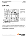
documents have been copied here, including the DSP56300 Family Manual (FamilyManual.pdf), the
DSP56301 User’s Manual (UsersManual.pdf), and the PCI application note AN1780 (PCI.pdf). Reference to these manuals will be made in this document.
Circuit Description
The DSP56301 operates at 3.3 volts, whereas the fiber optic parts operate at 5 volts. Toaccomodate the
two voltage requirements a 5 volt to 3.3 volts regulator is installed on the board, and only 5 volt power
is drawn from the edge connector. Several parts the EEPROM, FIFO and DRAM) were chosen in their
low voltage option. Two Cypress CY7C372I PALs operate from both 3.3 and 5 volt supplies and have
inputs that tolerate 5 volts and outputs that reach a maximum of 3.3 volts, providing a simple interface
between 3.3 and 5 volt parts.
The DSP is driven from the 33 MHz PCI bus clock, and employs an internal phase locked loop (PLL)
to multiply the input clock to its internal operating frequency of 78.4 MHz, s described in Section 2.1
of PCI.pdf, as follows PLL_INIT EQU
$750012
MOVEP #PLL_INIT,X:PCTL
; PLL = 33 MHz x 19 / 8 = 78.4 MHz
; Initialize PLL
The DSP boots from a 8k x 8 bit on-board EEPROM (Catalyst part number CAT28LV64P, any speed)
that operates at 3.3 volts. When the DSP RESET* signal makes a low to high transition the input lines
MODD to MODA are set to a 0001 by PAL U23 to cause the DSP to execute an internal program that
reads the DSP program from the EEPROM, and starts executing it from program address zero. The
RESET* line may be asserted low true by the host computer’s assertion of the PCIRST* line if the
jumper JP11 is installed. The Sun Microsystems Ultra 5 used for the interface board development
asserted this signal only during the power-up sequence and correctly released it several seconds prior
to accessing the interface board during the booting process. For host computers whose PCIRST* line
may not be well defined the jumper JP11 should be removed and booting accomplished instead from
a power-on reset circuit that asserts the RESET* line for several hundred milliseconds after the 5 volts
power has been turned on.
All DSP code executes from memory internal to the DSP, which must be loaded with the desired code.
There are three mechanisms for doing this. The boot code written to the EEPROM is generated with a
short script named "rom" that assembles and links a DSP source code file named "pciboot.asm"
written in assembly language with the assembler parameter DOWNLOAD=ROM to generate a
Motorola S-record file named "pci.s" that is loadable into an EEPROM burning machine. The script
"host" sets DOWNLOAD=HOST to generate a file named "pci.lod" that can be downloaded via the
host over the PCI bus to the DSP. The script "once" sets DOWNLOAD=ONCE to generate a file
named "pci.lod" that can be loaded into the DSP with the OnCE in-circuit emulator facility that
Motorola provides. The DSP source code file "pciboot.asm" has several conditional assembly
directives at the beginning to set execution and EEPROM load addresses to certain values depending
on the DOWNLOAD parameter, and to follow the protocol of the three different solftware loading
mechanisms. To summarize -
PCI Interface Board, pg. #2
Updated Dec. 2, 1999