1
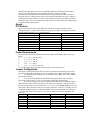
case the upper 12 bits (31:20) define the base PCI address. Therefore only 1
Mbyte of contiguous PCI memory space can be addressed. Figure xx illustrates
how a MBUS address is converted to a PCI address.
The FPGA requires the PCI target to handle 64 bit transfers and does not check
if the 64 bit transfer is not allowed. That means it cannot be used to address the
two other FPGAs on the Alpha board as those only handle 32 bit transfers. It
also currently does not respond to the PCI STOP signal that might be returned
by the target. This is a potential bug and will be fixed in an updated design.
Currently the state machines that handle MBUS transactions are synchronized to
the PCI clock. This means a 30ns delay between state transitions. Although this
simplifies the design, it results in a performance penalty. Once the prototype
design is working on the Alpha board, the FPGA will be changed so that the
MBUS state machines are asynchronous to improve MBUS performance.
Configuration
The MAGICFPGA is configured by writing to the appropriate configuration registers
according to the PCI specification. The MAGICFPGA responds to configuration reads
and writes when IDSEL 21 is driven.
The MAGICFPGA asks for 3 separate 16 bit (64 K) memory address spaces. The first is
for on chip registers which hold the PCI to MBUS translation address, as well as the
MBUS address space reserved for the chip. The other two address spaces are PCI
addresses defining Window A and Window B.
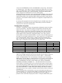
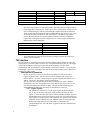
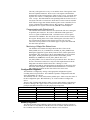
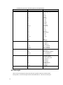
Table xx lists the values of the PCI configuration space. Bits indicated by “X” must be
written to configure the device. The last 3 bits of address 04h should be written as 110 to
enable memory reads/writes to the device as well as PCI bus mastership.
In principle, the PCI memory addresses should be set by the plug-n-play PCI protocol. In
that case user software would simply read these configuration registers to know what PCI
addresses to use for that device. However, the configuration registers can be changed at
any time by user software. In that case the software should be careful to not configure the
device with a PCI address used by another device on the board.
31
16 15
0 Address (hex)
Description
0x2CDF
0x2DEA
00h
Device ID
Vendor ID
7