1
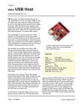
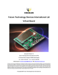
Future Technology Devices International Ltd.
VDIP2
Vinculum VNC1L Module
Datasheet
Document Reference No.: FT_000017
Version 1.0
Issue Date: 2010-03-08
Future Technology Devices International Ltd (FTDI)
Unit 1, 2 Seaward Place, Centurion Business Park, Glasgow, G41 1HH, United Kingdom
Tel.: +44 (0) 141 429 2777
Fax: + 44 (0) 141 429 2758
E-Mail (Support): [email protected]
Web: http://www.vinculum.com
Neither the whole nor any part of the information contained in, or the product described in this manual, may be adapted or reproduced
in any material or electronic form without the prior written consent of the copyright holder. This product and its documentation are
supplied on an as-is basis and no warranty as to their suitability for any particular purpose is either made or implied. Future Technology
Devices International Ltd will not accept any claim for damages howsoever arising as a result of use or failure of this product. Your
statutory rights are not affected. This product or any variant of it is not intended for use in any medical appliance, device or system in
which the failure of the product might reasonably be expected to result in personal injury. This document provides preliminar y
information that may be subject to change without notice. No freedom to use patents or other intellectual property rights is implied by
the publication of this document. Future Technology Devices International Ltd, Unit 1, 2 Seaward Place, Centurion Business Park,
Glasgow, G41 1HH, United Kingdom. Scotland Registered Number: SC136640
Copyright © 2010 Future Technology Devices International Limited
Document Reference No.: FT_000017
VDIP2 Vinculum VNC1L Module Datasheet Version 1.0
Clearance No.: FTDI# 145
`
1
Introduction
The VDIP2 module is an MCU to embedded USB host controller development module for the VNC1L I.C.
device.The VDIP2 is supplied on a PCB designed to fit into a 40 pin DIP socket, and provides access to
the UART, parallel FIFO, and SPI interface pins on the VNC1L device, via its AD and AC bus pins. All other
Vinculum I/O pins are also accessable. Not only is it ideal for developing and rapid prototyping of VNC1L
designs, but also an attractive quantity discount structure makes this module suitable for incorporation
into low and medium volume finished product designs.
Figure 1.1- VDIP2
The Vinculum VNC1L is the first of FTDI’s Vinculum family of Embedded USB host controller integrated
circuit devices. Not only is it able to handle the USB Host Interface, and data transfer functions but owing
to the inbuilt MCU and embedded Flash memory, Vinculum can encapsulate the USB device classes as
well. When interfacing to mass storage devices such as USB Flash drives, Vinculum also transparently
handles the FAT File structure communicating via UART, SPI or parallel FIFO interfaces via a simple to
implement command set. Vinculum provides a new cost effective solution for providing USB Host
capability into products that previously did not have the hardware resources available. The VNC1L is
available in Pb-free (RoHS compliant) compact 48-Lead LQFP package.
Copyright © 2009 Future Technology Devices International Limited
1
Document Reference No.: FT_000017
VDIP2 Vinculum VNC1L Module Datasheet Version 1.0
Clearance No.: FTDI# 145
`
Table of Contents
1
Introduction .................................................................... 1
2
Features .......................................................................... 3
3
Pin Out and Signal Description ........................................ 4
3.1
Module Pin Out.......................................................................... 4
3.2
Pin Signal Description ............................................................... 5
3.3
I/O Configuration Using The Jumper Pin Header ...................... 7
3.4
Default Interface I/O Pin Configuration .................................... 8
3.5
Signal Descriptions - UART Interface ........................................ 9
3.6
Signal Descriptions – Serial Peripheral Interface (SPI) ......... 10
3.6.1
SPI Slave Data Read Cycle ....................................................................... 10
3.6.2
SPI Slave Data Write Cycle ....................................................................... 11
SPI Slave Data Timing Diagrams ............................................................... 12
3.6.3
3.7
4
12
Signal Descriptions - Parallel FIFO Interface .......................... 13
3.7.1
Timing Diagram – Parallel FIFO Read Transaction ........................................ 14
3.7.2
Timing Diagram - Parallel FIFO Write Transaction ........................................ 15
Firmware....................................................................... 16
4.1.1
Firmware Support .................................................................................... 16
4.1.2
Firmware Upgrades .................................................................................. 16
5
Mechanical Dimensions ................................................. 17
6
Schematic Diagram ....................................................... 18
7
Contact Information ...................................................... 19
Appendix A – References ................................................................. 20
Appendix B – List of Figures and Tables .......................................... 21
List of Figures ................................................................................. 21
List of Tables ................................................................................... 21
Appendix C – Revision History ......................................................... 22
Copyright © 2009 Future Technology Devices International Limited
2
Document Reference No.: FT_000017
VDIP2 Vinculum VNC1L Module Datasheet Version 1.0
Clearance No.: FTDI# 145
`
2
Features
The VDIP2 has the following features:
Uses FTDI’s VNC1L embedded dual USB host
controller IC device
Program or update firmware via USB Flash
disk or via UART/Parallel FIFO/SPI interface
Two vertically mounted USB ‘A’ type USB
socket to interface with USB peripheral devices
Power and traffic indicator LED’s
Jumper selectable UART, parallel FIFO or SPI
MCU interfaces
VNC1L firmware programming control pins
PROG# and RESET# brought out onto jumper
interface
Single 5V supply input from USB connection
(no external supply necessary)
VDIP2 is a Pb-free, RoHS complaint
development module.
Auxiliary 3.3 V / 200 mA power output to
external logic.
Schematics, and firmware files available for
download from the Vinculum website
Copyright © 2009 Future Technology Devices International Limited
3
Document Reference No.: FT_000017
VDIP2 Vinculum VNC1L Module Datasheet Version 1.0
Clearance No.: FTDI# 145
`
3
Pin Out and Signal Description
3.1 Module Pin Out
Figure 3.1 – VDIP2 Module Pin Out (Top View)
Copyright © 2009 Future Technology Devices International Limited
4
Document Reference No.: FT_000017
VDIP2 Vinculum VNC1L Module Datasheet Version 1.0
Clearance No.: FTDI# 145
`
3.2 Pin Signal Description
Pin No.
Name
Pin Name
on PCB
Type
Description
1
NC
2
5V0
5V0
PWR Input
5.0 V module supply pin. This pin provides the 5.0V output on
the USB ‘A’ type socket, and also the 3.3V supply to VNCL2,
via an on-board 3.3 V L.D.O.
3
5V0
5V0
PWR Input
5.0 V module supply pin. This pin provides the 5.0V output on
the USB ‘A’ type socket, and also the 3.3V supply to VNCL2,
via an on-board 3.3 V L.D.O.
4
LED1
LD1
Output
USB port 1 traffic activity indicator LED. This pin is hard wired to
a green LED on board the PCB. It is also brought out onto this
pin which allows for the possibility of bring- ing out an additional
LED traffic indicator out of the VDIP2 board. For example, if the
VDIP2 USB connector is brought out onto an instrument front
panel, an activity LED could be mounted along side it.
5
LED2
LD2
Output
USB port 2 traffic activity indicator LED. This pin is hard wired to
a green LED on board the PCB. It is also brought out onto this
pin which allows for the possibility of bring- ing out an additional
LED traffic indicator out of the VDIP2 board. For example, if the
VDIP2 USB connector is brought out onto an instrument front
panel, an activity LED could be mounted along side it.
6
7
8
BDBUS7
BCBUS0
BCBUS1
BD7
BC0
BC1
I/O
I/O
I/O
Not connnected
9
5V0
5V0
PWR Input
10
BCBUS2
BC2
I/O
5V safe bidirectional data / control bus, BD bit 7
5V safe bidirectional data / control bus, BC bit 0
5V safe bidirectional data / control bus, BC bit 1
5.0 V module supply pin. This pin provides the 5.0V output on
the USB ‘A’ type socket, and also the 3.3V supply to VNC1L, via
an on-board 3.3 V L.D.O.
5V safe bidirectional data / control bus, BC bit 2
11
12
13
14
15
16
17
18
19
20
21
BCBUS3
GND
GND
ADBUS0
GND
ADBUS1
ADBUS2
ADBUS3
ADBUS4
ADBUS5
ADBUS6
BC3
GND
GND
AD0
GND
AD1
AD2
AD3
AD4
AD5
AD6
I/O
PWR
PWR
I/O
PWR
I/O
I/O
I/O
I/O
I/O
I/O
5V safe bidirectional data /
Module ground supply pin
Module ground supply pin
5V safe bidirectional data /
Module ground supply pin
5V safe bidirectional data /
5V safe bidirectional data /
5V safe bidirectional data /
5V safe bidirectional data /
5V safe bidirectional data /
5V safe bidirectional data /
22
ADBUS7
AD7
I/O
5V safe bidirectional data / control bus, AD bit 7
23
ACBUS0
AC0
I/O
5V safe bidirectional data / control bus, AC bit 0
24
ACBUS1
AC1
I/O
5V safe bidirectional data / control bus, AC bit 1
26
GND
GND
PWR
Module ground supply pin
27
ACBUS3
AC3
I/O
5V safe bidirectional data / control bus, AC bit 3
28
ACBUS4
AC4
I/O
5V safe bidirectional data / control bus, AC bit 4
29
ACBUS5
AC5
I/O
5V safe bidirectional data / control bus, AC bit 5
30
RESET#
RS#
Input
31
PROG#
PG#
Input
32
3V3
3V3
control bus, BC bit 3
control bus, AD bit 0
control
control
control
control
control
control
bus,
bus,
bus,
bus,
bus,
bus,
AD
AD
AD
AD
AD
AD
bit
bit
bit
bit
bit
bit
1
2
3
4
5
6
Can be used by an external device to reset the VNC1L. This pin
can be used in combi- nation with PROG# and the UART /
parallel FIFO / SPI interface to program firmware into the
VNC1L.
This
pin is used in combination with the RESET# pin and the
UART / parallel FIFO /
PWR Output 3.3V output from VDIP2’s on board 3.3V L.D.O.
Table 3.1 - Pin Signal Descriptions
Copyright © 2009 Future Technology Devices International Limited
5
Document Reference No.: FT_000017
VDIP2 Vinculum VNC1L Module Datasheet Version 1.0
Clearance No.: FTDI# 145
`
Pin No.
Name
Pin Name
on PCB
Type
Description
33
BDBUS0
BD0
I/O
5V safe bidirectional data / control bus, BD bit 0
34
35
36
37
BDBUS1
BDBUS2
BDBUS3
BDBUS4
BD1
BD2
BD3
BD4
I/O
I/O
I/O
I/O
5V
5V
5V
5V
38
3V3
3V3
PWR Output
3.3V output from VDIP2’s on board 3.3V L.D.O.
39
3V3
3V3
PWR Output
3.3V output from VDIP2’s on board 3.3V L.D.O.
40
NC
safe
safe
safe
safe
bidirectional
bidirectional
bidirectional
bidirectional
data
data
data
data
/
/
/
/
control
control
control
control
bus,
bus,
bus,
bus,
BD
BD
BD
BD
bit
bit
bit
bit
1
2
3
4
No Connect
Table 3.1 - Pin Signal Descriptions
Copyright © 2009 Future Technology Devices International Limited
6
Document Reference No.: FT_000017
VDIP2 Vinculum VNC1L Module Datasheet Version 1.0
Clearance No.: FTDI# 145
`
3.3 I/O Configuration Using The Jumper Pin Header
Two three way jumper pin headers are provided to allow for simple configuration of the I/O on data and
control bus pins of the VDIP2. This is done by a combination of pulling up or pulling down the VNC1L
ACBUS5 (pin 46) and ACBUS6 (pin 47). The relevant portion of the VDIP2 module schematic is shown in
Figure 3.2
Figure 3.2 – VDIP2 On-Board Jumper Pin Configuration.
ACBUS6
(VNC1L pin 47)
I/O Mode
ACBUS5
(VNC1L pin 46)
Pull-Up
Pull-Up
Serial UART
Pull-Up
Pull-Down
SPI
Pull-Down
Pull-Up
Parallel FIFO
Pull-Down
Pull-Down
Serial UART
Table 3.2 – VDIP2 Port Selection Jumper Pins
Copyright © 2009 Future Technology Devices International Limited
7
Document Reference No.: FT_000017
VDIP2 Vinculum VNC1L Module Datasheet Version 1.0
Clearance No.: FTDI# 145
`
3.4 Default Interface I/O Pin Configuration
The VNC1L device is pre-programmed with default settings for the I/O pins however they can be easily
changed to suit a designers needs. The default interface I/O pin configuration of the VNC1L device are
shown in Table 3.3
Pin
No.
14
16
17
18
19
20
21
22
23
24
25
27
Name
ADBUS0
ADBUS1
ADBUS2
ADBUS3
ADBUS4
ADBUS5
ADBUS6
ADBUS7
ACBUS0
ACBUS1
ACBUS2
ACBUS3
Pin
Name
on
PCB
AD0
AD1
AD2
AD3
AD4
AD5
AD6
AD7
AC0
AC1
AC2
AC3
Data and Control Bus Configuration
Options
Type
Description
UART
Interface
Parallel
FIFO
Interface
SPI Slave
Interface
I/O Port
I/O
5V safe bidirectional
data / control bus,
AD bit 0
TXD
D0
SCLK
PortAD0
I/O
5V safe bidirectional
data / control bus,
AD bit 1
RXD
D1
SDI
PortAD1
I/O
5V safe bidirectional
data / control bus,
AD bit 2
RTS#
D2
SDO
PortAD2
I/O
5V safe bidirectional
data / control bus,
AD bit 3
CTS#
D3
CS
PortAD3
I/O
5V safe bidirectional
data / control bus,
AD bit 4
DTR#
D4
NA
PortAD4
I/O
5V safe bidirectional
data / control bus,
AD bit 5
I/O
5V safe bidirectional
data / control bus,
AD bit 6
I/O
5V safe bidirectional
data / control bus,
AD bit 7
I/O
5V safe bidirectional
data / control bus,
AC bit 0
I/O
5V safe bidirectional
data / control bus,
AC bit 1
I/O
5V safe bidirectional
data / control bus,
AC bit 2
I/O
5V safe bidirectional
data / control bus,
AC bit 3
5V safe bidirectional
data / control bus,
28
ACBUS4
AC4
I/O
AC bit 4
Table 3.3 - Default Interface I/O Pin Configuration
NA
DSR#
D5
PortAD5
NA
DCD#
D6
PortAD6
NA
RI#
D7
PortAD7
NA
TXDEN#
RXF#
NA
PortAC0
NA
TXE#
NA
PortAC1
NA
RD#
NA
PortAC2
NA
WR
NA
NA
Copyright © 2009 Future Technology Devices International Limited
PortAC3
NA
PortAC4
8
Document Reference No.: FT_000017
VDIP2 Vinculum VNC1L Module Datasheet Version 1.0
Clearance No.: FTDI# 145
`
3.5 Signal Descriptions - UART Interface
The UART interface I/O pin description of the VNC1L device are shown in Table 3.4
Pin No.
Name
Type
Description
14
TXD
Output
Transmit asynchronous data output
16
RXD
Input
Receive asynchronous data input
17
RTS#
Output
Request To Send Control Output / Handshake signal
18
CTS#
Input
Clear To Send Control Input / Handshake signal
19
DTR#
Output
Data Terminal Ready Control Output / Handshake signal
20
DSR#
Input
Data Set Ready Control Input / Handshake signal
21
DCD#
Input
Data Carrier Detect Control Input
Input
Ring Indicator Contro l Input. When the RemoteakeW up option is
enabled in the EEPROM, taking RI# low can be used to resume the PC
USB Host controller from suspend
22
RI#
23
TXDEN#
Input
Enable Transmit Data for RS485 designs
Table 3.4 - Default I/O Pin Configuration – UART Interface
Copyright © 2009 Future Technology Devices International Limited
9
Document Reference No.: FT_000017
VDIP2 Vinculum VNC1L Module Datasheet Version 1.0
Clearance No.: FTDI# 145
`
3.6 Signal Descriptions – Serial Peripheral Interface (SPI)
The SPI I/O pin description of the VNC1L device are shown in Table 3.5
Pins No
Name
Type
Description
14
SCLK
Input
SPI Clock input, 12MHz maximum.
16
SDI
Input
SPI Serial Data Input
17
SDO
Output
SPI Serial Data Output
18
CS
Input
SPI Chip Select Input
Table 3.5 - Data and Control Bus Signal Mode Options – SPI Slave Interface
3.6.1 SPI Slave Data Read Cycle
When in SPI mode, the timing of a read operation is shown in Figure 3.3
Figure 3.3 – SPI Slave Data Read Cycle.
From Start - SPI CS must be held high for the entire read cycle, and must be taken low for at least one
clock period after t he read is co mpleted. The first bit on SPI Data In is the R/W bit - inputting a ‘1’ here
a llows data to be read fro m the chip. The next bit is the address bit, ADD, which is used to indicate
whether the data register (‘0’) or the status register (‘1’) is read from. During the SPI read cycle a byte of
data will start being output on SPI Data Out on the next clock cycle after t he address bit, MSBAfterfirst.t
he data has been clocked out of the chip, t he status of SPI Data. Out should be checked to see if the
data read is new data. A ‘0’ level here on SPI Data Out means that the data read is new data. A ‘1’
indicates that the data read is old data, and the read cycle should be repeated to get new data.
Remember that CS must be held low for at least one clock period before being taken high again to
continue with the next read or write cycle.
Copyright © 2009 Future Technology Devices International Limited
10
Document Reference No.: FT_000017
VDIP2 Vinculum VNC1L Module Datasheet Version 1.0
Clearance No.: FTDI# 145
`
3.6.2 SPI Slave Data Write Cycle
When in SPI mode, the timing of a write operation is shown in
Figure 3.4 – SPI Slave Data Write Cycle.
From Start - SPI CS must be held high for the entire write cycle, and must be taken low for at least
one clock period after t he write is co mpletedThe. first bit on SPI Data In is the R/W bit - inputting
a ‘0’ here a llows data to be written to the chip. The next bit is the address bit, ADD, which is used
to indicate whether the data register (‘0’) or the status register (‘1’) is written to. During the SPI
write cycle a byte of data can be input to SPI Data In on the next clock cycle after t he address bit,
MSBAfterfirst.t he data has been clocked in to the chip, t he status of SPI Data Out should be
checked to see if the data read was accepted. A ‘0’ level on SPI Data Out means that the data
write was accepted. A ‘1’ indicates that the internal buffer is full, and the write should be repeated.
Remember that CS must be held low for at least one clock period before being taken high again to
continue with the next read or write cycle.
Copyright © 2009 Future Technology Devices International Limited
11
Document Reference No.: FT_000017
VDIP2 Vinculum VNC1L Module Datasheet Version 1.0
Clearance No.: FTDI# 145
`
3.6.3 SPI Slave Data Timing Diagrams
Figure 3.5 – SPI Slave Data Timing Diagrams.
Time
Description
Min
T1
SPICLK Period
83
T2
SPICLK High
20
T3
SPICLK Low
20
T4
Input Setup Time
10
T5
Input Hold Time
10
T6
Output Hold Time
2
T7
Output Valid Time
Table 3.6 - SPI Slave Data Timing
Time
-
Typical
Max
Unit
-
-
ns
-
-
ns
-
-
ns
-
-
ns
-
-
ns
-
-
ns
-
20
ns
Description
0
RXF#
1
TXE#
2
-
3
-
4
RXF IRQEn
5
TXE IRQEn
6
-
7
Table 3.7 - SPI Slave Status Register (ADD=’1’)
Copyright © 2009 Future Technology Devices International Limited
12
Document Reference No.: FT_000017
VDIP2 Vinculum VNC1L Module Datasheet Version 1.0
Clearance No.: FTDI# 145
`
3.7 Signal Descriptions - Parallel FIFO Interface
The Parallel FIFO interface I/O pin description of the VNC1L device is shown in Table 3.8
Pin No.
Name
Type
Description
14
D0
I/O
FIFO Data Bus Bit 0
16
D1
I/O
FIFO Data Bus Bit 1
17
D2
I/O
FIFO Data Bus Bit 2
18
D3
I/O
FIFO Data Bus Bit 3
19
D4
I/O
FIFO Data Bus Bit 4
20
D5
I/O
FIFO Data Bus Bit 5
21
D6
I/O
FIFO Data Bus Bit 6
22
D7
I/O
FIFO Data Bus Bit 7
23
RXF#
OUTPUT
When high, do not read data from the FIFO. When low, there is data
available in the FIFO which can be read by stro bing RD# low, then high
again.
24
TXE#
OUTPUT
When high, do not write data into the FIFO. When low, data can be
written into the FIFO by strobing WR high, then low.
INPUT
Enables the current
FIFO data byte on D0...D7 when low. Fetched the
next FIFO data byte (if avail- able) fro m the recei ve FIFO buffer w hen
RD# goes fro m high to low
25
RD#
Writes the data byte on the D0...D7 pins into the transmit FIFO buffer
27
WR
INPUT
when WR goes from high to low.
Table 3.8 - Default Interface I/O Pin Configuration Option – Paralle FIFO Interface
Copyright © 2009 Future Technology Devices International Limited
13
Document Reference No.: FT_000017
VDIP2 Vinculum VNC1L Module Datasheet Version 1.0
Clearance No.: FTDI# 145
`
3.7.1 Timing Diagram – Parallel FIFO Read Transaction
When in parallel FIFO interface mode, the timing of a read is shown in Figure 3.6 and Table 3.9
Figure 3.6 - FIFO Read Cycle.
Time
Description
Min
Max
Unit
T1
RD# Active Pulse Width
50
-
ns
T2
RD# to RD# Pre-Charge Time
50 + T6
-
ns
T3
RD# Active to Valid Data*
20
50
ns
T4
0
-
ns
T5
Valid Data Hold Time from RD#
Inactive*
RD# Inactive to RXF#
0
25
ns
T6
RXF# Inactive After RD# Cycle
80
-
ns
Table 3.9 FIFO Read Cycle Timing
* Load = 30pF
Copyright © 2009 Future Technology Devices International Limited
14
Document Reference No.: FT_000017
VDIP2 Vinculum VNC1L Module Datasheet Version 1.0
Clearance No.: FTDI# 145
`
3.7.2 Timing Diagram - Parallel FIFO Write Transaction
When in parallel FIFO interface mode, the timing of a write operation is shown in Figure 3.7 and Table
3.10
Figure 3.7 - FIFO Write Cycle.
Time
Description
Min
Max
Unit
T7
WR Active Pulse Width
50
-
ns
T8
WR to WR Pre-Charge Time
50
-
ns
T9
WR Active to Valid Data
20
-
ns
T10
Data Hold Time from WR
Inactive*
WR Inactive to TXE#
0
-
ns
T11
5
25
ns
T12
TXE# Inactive After WR Cycle
80
-
ns
Table 3.10 - FIFO Write Cycle Timing
Copyright © 2009 Future Technology Devices International Limited
15
Document Reference No.: FT_000017
VDIP2 Vinculum VNC1L Module Datasheet Version 1.0
Clearance No.: FTDI# 145
`
4
Firmware
4.1.1 Firmware Support
There are currently 6 standard firmware versions available for VDIP2 module which can be downloaded
from the FTDI website.
VDAP Firmware: USB Host for single Flash Disk and General Purpose USB peripherals. Selectable
UART, FIFO or SPI interface command monitor.
VDPS Firmware: USB Host for single Flash Disk and General Purpose USB peripherals. USB Slave
port connection for connecting to host PC. Selectable UART, FIFO or SPI interface command
monitor.
VDFC Firmware: USB Host for two Flash Disks, Selectable UART, FIFO or SPI interface command
monitor.
VCDC Firmware: USB Host for automatic connection to USB Communications Class Devices. UART
interface command monitor.
VDIF Firmware: USB Host for single Flash Disk and General Purpose USB peripherals. Selectable
UART, FIFO, SPI or USB interface command monitor.
4.1.2 Firmware Upgrades
The VDIP2 module is supplied pre-loaded with the VDAP firmware.
There are two methods of upgrading the firmware on the VDIP2. These methods are described in a
Vinculum Firmware manual please refer to:http://www.vinculum.com/documents/fwspecs/UM_VinculumFirmware_V205.pdf
Copyright © 2009 Future Technology Devices International Limited
16
Document Reference No.: FT_000017
VDIP2 Vinculum VNC1L Module Datasheet Version 1.0
Clearance No.: FTDI# 145
`
5
Mechanical Dimensions
Figure 5.1 VDIP2 Dimensions (Top View)
Figure 5.2 VDIP2 Dimensions (Side View)
Copyright © 2009 Future Technology Devices International Limited
17
Document Reference No.: FT_000017
VDIP2 Vinculum VNC1L Module Datasheet Version 1.0
Clearance No.: FTDI# 145
`
6
Schematic Diagram
Figure 6.1 - Schematic Diagram
Copyright © 2009 Future Technology Devices International Limited
18
Document Reference No.: FT_000017
VDIP2 Vinculum VNC1L Module Datasheet Version 1.0
Clearance No.: FTDI# 145
`
7
Contact Information
Head Office – Glasgow, UK
Future Technology Devices International Limited
Unit 1, 2 Seaward Place,
Centurion Business Park
Glasgow, G41 1HH
United Kingdom
Tel: +44 (0) 141 429 2777
Fax: +44 (0) 141 429 2758
E-mail (Sales)
[email protected]
E-mail (Support) [email protected]
E-mail (General Enquiries) [email protected]
Web Site URL
http://www.ftdichip.com
Web Shop URL
http://www.ftdichip.com
Branch Office – Taipei, Taiwan
Future Technology Devices International Limited (Taiwan)
2F, No 516, Sec. 1 NeiHu Road
Taipei 114
Taiwan, R.O.C.
Tel: +886 (0) 2 8791 3570
Fax: +886 (0) 2 8791 3576
E-mail (Sales)
[email protected]
E-mail (Support) [email protected]
E-mail (General Enquiries) [email protected]
Web Site URL
http://www.ftdichip.com
Branch Office – Hillsboro, Oregon, USA
Future Technology Devices International Limited (USA)
7235 NW Evergreen Parkway, Suite 600
Hillsboro, OR 97123-5803
USA
Tel: +1 (503) 547 0988
Fax: +1 (503) 547 0987
E-Mail (Sales)
[email protected]
E-Mail (Support) [email protected]
E-Mail (General Enquiries) [email protected]
Web Site URL
http://www.ftdichip.com
Branch Office – Shanghai, China
Future Technology Devices International Limited (China)
Room 408, 317 Xianxia Road,
ChangNing District,
ShangHai, China
Tel: +86 (21) 62351596
Fax: +86(21) 62351595
E-Mail (Sales): [email protected]
E-Mail (Support): [email protected]
E-Mail (General Enquiries): [email protected]
Web Site URL
http://www.ftdichip.com
Distributor and Sales Representatives
Please visit the Sales Network page of the FTDI Web site for the contact details of our distributor(s) and sales
representative(s) in your country.
Copyright © 2009 Future Technology Devices International Limited
19
Document Reference No.: FT_000017
VDIP2 Vinculum VNC1L Module Datasheet Version 1.0
Clearance No.: FTDI# 145
`
Appendix A – References
http://www.vinculum.com/documents/fwspecs/UM_VinculumFirmware_V205.pdf
Copyright © 2009 Future Technology Devices International Limited
20
Document Reference No.: FT_000017
VDIP2 Vinculum VNC1L Module Datasheet Version 1.0
Clearance No.: FTDI# 145
`
Appendix B – List of Figures and Tables
List of Figures
Figure 1.1- VDIP2 ......................................................................................................................... 1
Figure 3.1 – VDIP2 Module Pin Out (Top View) ................................................................................. 4
Figure 3.2 – VDIP2 On-Board Jumper Pin Configuration. ................................................................... 7
Figure 3.3 – SPI Slave Data Read Cycle. ........................................................................................ 10
Figure 3.4 – SPI Slave Data Write Cycle. ....................................................................................... 11
Figure 3.5 – SPI Slave Data Timing Diagrams................................................................................. 12
Figure 3.6 - FIFO Read Cycle. ....................................................................................................... 14
Figure 3.7 - FIFO Write Cycle. ...................................................................................................... 15
Figure 5.1 VDIP2 Dimensions (Top View) ....................................................................................... 17
Figure 5.2 VDIP2 Dimensions (Side View) ...................................................................................... 17
Figure 7.1 - Schematic Diagram ................................................................................................... 18
List of Tables
Table 3.1 - Pin Signal Descriptions .................................................................................................. 5
Table 3.2 – VDIP2 Port Selection Jumper Pins .................................................................................. 7
Table 3.5 - Data and Control Bus Signal Mode Options – SPI Slave Interface ...................................... 10
Table 3.6 - SPI Slave Data Timing ................................................................................................ 12
Table 3.7 - SPI Slave Status Register (ADD=’1’) ............................................................................. 12
Table 3.8 - Default Interface I/O Pin Configuration Option – Paralle FIFO Interface ............................ 13
Table 3.9 FIFO Read Cycle Timing ................................................................................................. 14
Table 3.10 - FIFO Write Cycle Timing ............................................................................................ 15
Copyright © 2009 Future Technology Devices International Limited
21
Document Reference No.: FT_000017
VDIP2 Vinculum VNC1L Module Datasheet Version 1.0
Clearance No.: FTDI# 145
`
Appendix C – Revision History
Version 0.90
Initial Datasheet Created
March 2007
Version 0.91
Datasheet Updated table 4,5 and 8
April 2007
Version 1.0
Datasheet Updated (Reformatted)
08 March 2010
Datasheet Updated (Mechanical Drawings)
Added Appendix A and B
Added schematic
Copyright © 2009 Future Technology Devices International Limited
22