1
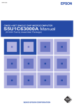
CMOS 16-BIT SINGLE CHIP MICROCOMPUTER
S1C17 Family
S1C17 Core Manual
NOTICE
No part of this material may be reproduced or duplicated in any form or by any means without the written permission
of Seiko Epson. Seiko Epson reserves the right to make changes to this material without notice. Seiko Epson does not
assume any liability of any kind arising out of any inaccuracies contained in this material or due to its application or
use in any product or circuit and, further, there is no representation that this material is applicable to products requiring high level reliability, such as medical products. Moreover, no license to any intellectual property rights is granted by
implication or otherwise, and there is no representation or warranty that anything made in accordance with this material will be free from any patent or copyright infringement of a third party. This material or portions thereof may contain
technology or the subject relating to strategic products under the control of the Foreign Exchange and Foreign Trade
Law of Japan and may require an export license from the Ministry of International Trade and Industry or other approval
from another government agency.
© SEIKO EPSON CORPORATION 2007, All rights reserved.
Configuration of product number
Devices
S1
C
17xxx
F
00E1
00
Packing specifications
00 : Besides tape & reel
0A : TCP BL
2 directions
0B : Tape & reel BACK
0C : TCP BR
2 directions
0D : TCP BT
2 directions
0E : TCP BD
2 directions
0F : Tape & reel FRONT
0G : TCP BT
4 directions
0H : TCP BD
4 directions
0J : TCP SL
2 directions
0K : TCP SR
2 directions
0L : Tape & reel LEFT
0M: TCP ST
2 directions
0N : TCP SD
2 directions
0P : TCP ST
4 directions
0Q : TCP SD
4 directions
0R : Tape & reel RIGHT
99 : Specs not fixed
Specification
Package
D: die form; F: QFP, B: BGA
Model number
Model name
C: microcomputer, digital products
Product classification
S1: semiconductor
Development tools
S5U1
C
17000
H2
1
00
Packing specifications
00: standard packing
Version
1: Version 1
Tool type
Hx : ICE
Dx : Evaluation board
Ex : ROM emulation board
Mx : Emulation memory for external ROM
Tx : A socket for mounting
Cx : Compiler package
Sx : Middleware package
Corresponding model number
17xxx: for S1C17xxx
Tool classification
C: microcomputer use
Product classification
S5U1: development tool for semiconductor products
CONTENTS
– Contents –
1 Summary .......................................................................................................................1-1
1.1 Features ...........................................................................................................................1-1
2 Registers .......................................................................................................................2-1
2.1
2.2
2.3
2.4
General-Purpose Registers (R0–R7) ...............................................................................2-1
Program Counter (PC) .....................................................................................................2-1
Processor Status Register (PSR).....................................................................................2-2
Stack Pointer (SP) ............................................................................................................2-4
2.4.1 About the Stack Area .........................................................................................2-4
2.4.2 SP Operation at Subroutine Call/Return ............................................................2-4
2.4.3 SP Operation when an Interrupt Occurs ............................................................2-5
2.4.4 Saving/Restoring Register Data Using a Load Instruction ................................2-6
2.5 Register Notation and Register Numbers ........................................................................2-7
2.5.1 General-Purpose Registers ...............................................................................2-7
2.5.2 Special Registers ...............................................................................................2-7
3 Data Formats.................................................................................................................3-1
3.1 Data Formats Handled in Operations Between Registers ...............................................3-1
3.1.1 Unsigned 8-Bit Transfer (Register → Register) ..................................................3-1
3.1.2 Signed 8-Bit Transfer (Register → Register) ......................................................3-1
3.1.3 16-Bit Transfer (Register → Register) ................................................................3-2
3.1.4 24-Bit Transfer (Register → Register) ................................................................3-2
3.2 Data Formats Handled in Operations Between Memory and a Register .........................3-2
3.2.1
3.2.2
3.2.3
3.2.4
3.2.5
3.2.6
3.2.7
Unsigned 8-Bit Transfer (Memory → Register) ..................................................3-3
Signed 8-Bit Transfer (Memory → Register) ......................................................3-3
8-Bit Transfer (Register → Memory) ..................................................................3-3
16-Bit Transfer (Memory → Register) ................................................................3-3
16-Bit Transfer (Register → Memory) ................................................................3-4
32-Bit Transfer (Memory → Register) ................................................................3-4
32-Bit Transfer (Register → Memory) ................................................................3-4
4 Address Map .................................................................................................................4-1
4.1 Address Space .................................................................................................................4-1
4.2 Processor Information in the Core I/O Area ....................................................................4-2
4.2.1 Trap Table Base Register (TTBR, 0xffff80).........................................................4-2
4.2.2 Processor ID Register (IDIR, 0xffff84) ...............................................................4-2
4.2.3 Debug RAM Base Register (DBRAM, 0xffff90)..................................................4-2
5 Instruction Set ..............................................................................................................5-1
5.1 List of Instructions ............................................................................................................5-1
5.2 Addressing Modes (without ext extension) .....................................................................5-5
5.2.1 Immediate Addressing .......................................................................................5-5
5.2.2 Register Direct Addressing ................................................................................5-5
5.2.3 Register Indirect Addressing ..............................................................................5-6
5.2.4 Register Indirect Addressing with Post-increment/decrement or Pre-decrement ... 5-6
5.2.5 Register Indirect Addressing with Displacement ...............................................5-7
5.2.6 Signed PC Relative Addressing ........................................................................5-7
5.2.7 PC Absolute Addressing ....................................................................................5-7
S1C17 FAMILY S1C17 CORE MANUAL
EPSON
i
CONTENTS
5.3 Addressing Modes with ext.............................................................................................5-8
5.3.1 Extension of Immediate Addressing ..................................................................5-8
5.3.2 Extension of Register Direct Addressing ...........................................................5-9
5.3.3 Extension of Register Indirect Addressing ........................................................5-10
5.3.4 Extension of Register Indirect Addressing with Displacement ..........................5-11
5.3.5 Extension of Signed PC Relative Addressing ...................................................5-11
5.3.6 Extension of PC Absolute Addressing ..............................................................5-12
5.4 Data Transfer Instructions ...............................................................................................5-13
5.5
5.6
5.7
5.8
Logical Operation Instructions.........................................................................................5-14
Arithmetic Operation Instructions ....................................................................................5-15
Shift and Swap Instructions.............................................................................................5-16
Branch and Delayed Branch Instructions ........................................................................5-17
5.8.1 Types of Branch Instructions .............................................................................5-17
5.8.2 Delayed Branch Instructions .............................................................................5-21
5.9 System Control Instructions ............................................................................................5-22
5.10 Conversion Instructions .................................................................................................5-23
5.11 Coprocessor Instructions ..............................................................................................5-24
6 Functions ......................................................................................................................6-1
6.1 Transition of the Processor Status ....................................................................................6-1
6.1.1 Reset State ........................................................................................................6-1
6.1.2 Program Execution State ...................................................................................6-1
6.1.3 Interrupt Handling ..............................................................................................6-1
6.1.4 Debug Interrupt ..................................................................................................6-1
6.1.5 HALT and SLEEP Modes ...................................................................................6-1
6.2 Program Execution ...........................................................................................................6-2
6.2.1 Instruction Fetch and Execution .........................................................................6-2
6.2.2 Execution Cycles and Flags...............................................................................6-3
6.3 Interrupts ..........................................................................................................................6-6
6.3.1 Priority of Interrupts ...........................................................................................6-6
6.3.2 Vector Table........................................................................................................6-7
6.3.3 Interrupt Handling ..............................................................................................6-7
6.3.4 Reset .................................................................................................................6-7
6.3.5 Address Misaligned Interrupt .............................................................................6-8
6.3.6 NMI ....................................................................................................................6-8
6.3.7 Maskable External Interrupts .............................................................................6-8
6.3.8 Software Interrupts ............................................................................................6-9
6.3.9 Interrupt Masked Period.....................................................................................6-9
6.4 Power-Down Mode ..........................................................................................................6-10
6.5 Debug Circuit ..................................................................................................................6-11
6.5.1 Debugging Functions ........................................................................................6-11
6.5.2 Resource Requirements and Debugging Tools.................................................6-11
6.5.3 Registers for Debugging ...................................................................................6-12
7 Details of Instructions ..................................................................................................7-1
adc
adc/c
adc/nc
adc
add
add/c
add/nc
add
add.a
ii
%rd, %rs ............................................................................................................................. 7-2
%rd, %rs ............................................................................................................................. 7-2
%rd, %rs ............................................................................................................................. 7-2
%rd, imm7 .......................................................................................................................... 7-3
%rd, %rs ............................................................................................................................. 7-4
%rd, %rs ............................................................................................................................. 7-4
%rd, %rs ............................................................................................................................. 7-4
%rd, imm7 .......................................................................................................................... 7-5
%rd, %rs ............................................................................................................................. 7-6
EPSON
S1C17 FAMILY S1C17 CORE MANUAL
CONTENTS
add.a/c
add.a/nc
add.a
add.a
add.a
and
and/c
and/nc
and
brk
call
call.d
call
call.d
calla
calla.d
calla
calla.d
cmc
cmc/c
cmc/nc
cmc
cmp
cmp/c
cmp/nc
cmp
cmp.a
cmp.a/c
cmp.a/nc
cmp.a
cv.ab
cv.al
cv.as
cv.la
cv.ls
di
ei
ext
halt
int
intl
jpa
jpa.d
jpa
jpa.d
jpr
jpr.d
jpr
jpr.d
jreq
jreq.d
jrge
jrge.d
jrgt
jrgt.d
jrle
jrle.d
jrlt
%rd, %rs ............................................................................................................................. 7-6
%rd, %rs ............................................................................................................................. 7-6
%rd, imm7 .......................................................................................................................... 7-7
%sp, %rs ............................................................................................................................ 7-8
%sp, imm7 ......................................................................................................................... 7-9
%rd, %rs ............................................................................................................................ 7-10
%rd, %rs ............................................................................................................................ 7-10
%rd, %rs ............................................................................................................................ 7-10
%rd, sign7 ......................................................................................................................... 7-11
........................................................................................................................................... 7-12
%rb .................................................................................................................................... 7-13
%rb .................................................................................................................................... 7-13
sign10 ................................................................................................................................ 7-14
sign10 ................................................................................................................................ 7-14
%rb .................................................................................................................................... 7-15
%rb .................................................................................................................................... 7-15
imm7 .................................................................................................................................. 7-16
imm7 .................................................................................................................................. 7-16
%rd, %rs ............................................................................................................................ 7-17
%rd, %rs ............................................................................................................................ 7-17
%rd, %rs ............................................................................................................................ 7-17
%rd, sign7 ......................................................................................................................... 7-18
%rd, %rs ............................................................................................................................ 7-19
%rd, %rs ............................................................................................................................ 7-19
%rd, %rs ............................................................................................................................ 7-19
%rd, sign7 ......................................................................................................................... 7-20
%rd, %rs ............................................................................................................................ 7-21
%rd, %rs ............................................................................................................................ 7-21
%rd, %rs ............................................................................................................................ 7-21
%rd, imm7 ......................................................................................................................... 7-22
%rd, %rs ............................................................................................................................ 7-23
%rd, %rs ............................................................................................................................ 7-24
%rd, %rs ............................................................................................................................ 7-25
%rd, %rs ............................................................................................................................ 7-26
%rd, %rs ............................................................................................................................ 7-27
........................................................................................................................................... 7-28
........................................................................................................................................... 7-29
imm13 ................................................................................................................................ 7-30
........................................................................................................................................... 7-31
imm5 .................................................................................................................................. 7-32
imm5, imm3 ...................................................................................................................... 7-33
%rb .................................................................................................................................... 7-34
%rb .................................................................................................................................... 7-34
imm7 .................................................................................................................................. 7-35
imm7 .................................................................................................................................. 7-35
%rb .................................................................................................................................... 7-36
%rb .................................................................................................................................... 7-36
sign10 ................................................................................................................................ 7-37
sign10 ................................................................................................................................ 7-37
sign7 .................................................................................................................................. 7-38
sign7 .................................................................................................................................. 7-38
sign7 .................................................................................................................................. 7-39
sign7 .................................................................................................................................. 7-39
sign7 .................................................................................................................................. 7-40
sign7 .................................................................................................................................. 7-40
sign7 .................................................................................................................................. 7-41
sign7 .................................................................................................................................. 7-41
sign7 .................................................................................................................................. 7-42
S1C17 FAMILY S1C17 CORE MANUAL
EPSON
iii
CONTENTS
jrlt.d
jrne
jrne.d
jruge
jruge.d
jrugt
jrugt.d
jrule
jrule.d
jrult
jrult.d
ld
ld
ld
ld
ld
ld
ld
ld
ld
ld
ld
ld
ld
ld
ld.a
ld.a
ld.a
ld.a
ld.a
ld.a
ld.a
ld.a
ld.a
ld.a
ld.a
ld.a
ld.a
ld.a
ld.a
ld.a
ld.a
ld.a
ld.a
ld.a
ld.a
ld.a
ld.a
ld.a
ld.a
ld.a
ld.b
ld.b
ld.b
ld.b
ld.b
ld.b
ld.b
ld.b
iv
sign7 .................................................................................................................................. 7-42
sign7 .................................................................................................................................. 7-43
sign7 .................................................................................................................................. 7-43
sign7 .................................................................................................................................. 7-44
sign7 .................................................................................................................................. 7-44
sign7 .................................................................................................................................. 7-45
sign7 .................................................................................................................................. 7-45
sign7 .................................................................................................................................. 7-46
sign7 .................................................................................................................................. 7-46
sign7 .................................................................................................................................. 7-47
sign7 .................................................................................................................................. 7-47
%rd, %rs ............................................................................................................................ 7-48
%rd, [%rb] ......................................................................................................................... 7-49
%rd, [%rb]+ ....................................................................................................................... 7-49
%rd, [%rb]- ........................................................................................................................ 7-49
%rd, -[%rb] ........................................................................................................................ 7-49
%rd, [%sp + imm7] ........................................................................................................... 7-51
%rd, [imm7] ....................................................................................................................... 7-52
%rd, sign7 ......................................................................................................................... 7-53
[%rb], %rs ......................................................................................................................... 7-54
[%rb]+, %rs ....................................................................................................................... 7-54
[%rb]-, %rs ........................................................................................................................ 7-54
-[%rb], %rs ........................................................................................................................ 7-54
[%sp + imm7], %rs ........................................................................................................... 7-56
[imm7], %rs ....................................................................................................................... 7-57
%rd, %pc ........................................................................................................................... 7-58
%rd, %rs ............................................................................................................................ 7-59
%rd, %sp ........................................................................................................................... 7-60
%rd, [%rb] ......................................................................................................................... 7-61
%rd, [%rb]+ ....................................................................................................................... 7-61
%rd, [%rb]- ........................................................................................................................ 7-61
%rd, -[%rb] ........................................................................................................................ 7-61
%rd, [%sp] ......................................................................................................................... 7-63
%rd, [%sp]+ ....................................................................................................................... 7-63
%rd, [%sp]-........................................................................................................................ 7-63
%rd, -[%sp]........................................................................................................................ 7-63
%rd, [%sp + imm7] ........................................................................................................... 7-65
%rd, [imm7] ....................................................................................................................... 7-66
%rd, imm7 ......................................................................................................................... 7-67
%sp, %rs ........................................................................................................................... 7-68
%sp, imm7 ........................................................................................................................ 7-69
[%rb], %rs ......................................................................................................................... 7-70
[%rb]+, %rs ....................................................................................................................... 7-70
[%rb]-, %rs ........................................................................................................................ 7-70
-[%rb], %rs ........................................................................................................................ 7-70
[%sp], %rs ......................................................................................................................... 7-72
[%sp]+, %rs ....................................................................................................................... 7-72
[%sp]-, %rs ........................................................................................................................ 7-72
-[%sp], %rs ........................................................................................................................ 7-72
[%sp + imm7], %rs ........................................................................................................... 7-74
[imm7], %rs ....................................................................................................................... 7-75
%rd, %rs ............................................................................................................................ 7-76
%rd, [%rb] ......................................................................................................................... 7-77
%rd, [%rb]+ ....................................................................................................................... 7-77
%rd, [%rb]- ........................................................................................................................ 7-77
%rd, -[%rb] ........................................................................................................................ 7-77
%rd, [%sp + imm7] ........................................................................................................... 7-79
%rd, [imm7] ....................................................................................................................... 7-80
[%rb], %rs ......................................................................................................................... 7-81
EPSON
S1C17 FAMILY S1C17 CORE MANUAL
CONTENTS
ld.b
ld.b
ld.b
ld.b
ld.b
ld.ca
ld.ca
ld.cf
ld.cf
ld.cw
ld.cw
ld.ub
ld.ub
ld.ub
ld.ub
ld.ub
ld.ub
ld.ub
nop
not
not/c
not/nc
not
or
or/c
or/nc
or
ret
ret.d
retd
reti
reti.d
sa
sa
sbc
sbc/c
sbc/nc
sbc
sl
sl
slp
sr
sr
sub
sub/c
sub/nc
sub
sub.a
sub.a/c
sub.a/nc
sub.a
sub.a
sub.a
swap
xor
xor/c
xor/nc
xor
[%rb]+, %rs ....................................................................................................................... 7-81
[%rb]-, %rs ........................................................................................................................ 7-81
-[%rb], %rs ........................................................................................................................ 7-81
[%sp + imm7], %rs ........................................................................................................... 7-83
[imm7], %rs ....................................................................................................................... 7-84
%rd, %rs ............................................................................................................................ 7-85
%rd, imm7 ......................................................................................................................... 7-86
%rd, %rs ............................................................................................................................ 7-87
%rd, imm7 ......................................................................................................................... 7-88
%rd, %rs ............................................................................................................................ 7-89
%rd, imm7 ......................................................................................................................... 7-90
%rd, %rs ............................................................................................................................ 7-91
%rd, [%rb] ......................................................................................................................... 7-92
%rd, [%rb]+ ....................................................................................................................... 7-92
%rd, [%rb]- ........................................................................................................................ 7-92
%rd, -[%rb] ........................................................................................................................ 7-92
%rd, [%sp + imm7] ........................................................................................................... 7-94
%rd, [imm7] ....................................................................................................................... 7-95
........................................................................................................................................... 7-96
%rd, %rs ............................................................................................................................ 7-97
%rd, %rs ............................................................................................................................ 7-97
%rd, %rs ............................................................................................................................ 7-97
%rd, sign7 ......................................................................................................................... 7-98
%rd, %rs ............................................................................................................................ 7-99
%rd, %rs ............................................................................................................................ 7-99
%rd, %rs ............................................................................................................................ 7-99
%rd, sign7 ........................................................................................................................ 7-100
.......................................................................................................................................... 7-101
.......................................................................................................................................... 7-101
.......................................................................................................................................... 7-102
.......................................................................................................................................... 7-103
.......................................................................................................................................... 7-103
%rd, %rs ........................................................................................................................... 7-104
%rd, imm7 ........................................................................................................................ 7-105
%rd, %rs ........................................................................................................................... 7-106
%rd, %rs ........................................................................................................................... 7-106
%rd, %rs ........................................................................................................................... 7-106
%rd, imm7 ........................................................................................................................ 7-107
%rd, %rs ........................................................................................................................... 7-108
%rd, imm7 ........................................................................................................................ 7-109
.......................................................................................................................................... 7-110
%rd, %rs ........................................................................................................................... 7-111
%rd, imm7 ........................................................................................................................ 7-112
%rd, %rs ........................................................................................................................... 7-113
%rd, %rs ........................................................................................................................... 7-113
%rd, %rs ........................................................................................................................... 7-113
%rd, imm7 ........................................................................................................................ 7-114
%rd, %rs ........................................................................................................................... 7-115
%rd, %rs ........................................................................................................................... 7-115
%rd, %rs ........................................................................................................................... 7-115
%rd, imm7 ........................................................................................................................ 7-116
%sp, %rs .......................................................................................................................... 7-117
%sp, imm7 ....................................................................................................................... 7-118
%rd, %rs ........................................................................................................................... 7-119
%rd, %rs ........................................................................................................................... 7-120
%rd, %rs ........................................................................................................................... 7-120
%rd, %rs ........................................................................................................................... 7-120
%rd, sign7 ........................................................................................................................ 7-121
S1C17 FAMILY S1C17 CORE MANUAL
EPSON
v
CONTENTS
Appendix List of S1C17 Core Instructions.................................................................. Ap-1
vi
EPSON
S1C17 FAMILY S1C17 CORE MANUAL
1 SUMMARY
1 Summary
The S1C17 Core is a Seiko Epson original 16-bit RISC-type processor.
It features low power consumption, high-speed operation with a maximum 60 MHz to 90 MHz clock, large address
space up to 16M bytes addressable, main instructions executable in one clock cycle, and a small sized design. The
S1C17 Core is suitable for embedded applications that do not need a lot of data processing power like the S1C33
Cores the high-end processors, such as controllers and sequencers for which an eight-bit CPU is commonly used.
The S1C17 Core incorporates a coprocessor interface allowing implementation of additional computing features.
Furthermore, Seiko Epson provides a software development environment similar to the S1C33 Family that includes
an IDE work bench, a C compiler, a serial ICE and a debugger, for supporting the developer to develop application
software.
1.1 Features
Processor type
• Seiko Epson original 16-bit RISC processor
• 0.35–0.15 µm low power CMOS process technology
Operating-clock frequency
• 90 MHz maximum (depending on the processor model and process technology)
Instruction set
• Code length:
16-bit fixed length
• Number of instructions:
111 basic instructions (184 including variations)
• Execution cycle:
Main instructions executed in one cycles
• Extended immediate instructions: Immediate extended up to 24 bits
• Compact and fast instruction set optimized for development in C language
Register set
• Eight 24-bit general-purpose registers
• Two 24-bit special registers
• One 8-bit special register
Memory space and bus
• Up to 16M bytes of memory space (24-bit address)
• Harvard architecture using separated instruction bus (16 bits) and data bus (32 bits)
Interrupts
• Reset, NMI, and 32 external interrupts supported
• Address misaligned interrupt
• Debug interrupt
• Direct branching from vector table to interrupt handler routine
• Programmable software interrupts with a vector number specified (all vector numbers specifiable)
Power saving
• HALT (halt instruction)
• SLEEP (slp instruction)
Coprocessor interface
• ALU instructions can be enhanced
S1C17 FAMILY S1C17 CORE MANUAL
EPSON
1-1
1 SUMMARY
THIS PAGE IS BLANK.
1-2
EPSON
S1C17 FAMILY S1C17 CORE MANUAL
2 REGISTERS
2 Registers
The S1C17 Core contains eight general-purpose registers and three special registers.
Special registers
bit 23
General-purpose registers
bit 0
PC
SP
bit 23
7
6
5
4
3
2
1
0
PSR
7
6
IL[2:0]
5
4
3
IE
C
2
1
V
Z
0
N
bit 0
R7
R6
R5
R4
R3
R2
R1
R0
Figure 2.1 Registers
2.1 General-Purpose Registers (R0–R7)
Register name
Symbol
R0–R7
General-Purpose Register
Size
R/W
Initial value
24 bits
R/W
0x000000 or indeterminate
The eight registers R0–R7 (r0–r7) are 24-bit general-purpose registers that can be used for data manipulation, data
transfer, memory addressing, or other general purposes. The contents of all of these registers are handled as 24-bit
data or addresses. 8- or 16-bit data can be sign- or zero-extended to a 24-bit quantity when it is loaded into one of
these registers using a load instruction or a conversion instruction. When these registers are used for address references, 24-bit memory space can be accessed directly.
At initial reset, the contents of the general-purpose registers are set to 0 (may be indeterminate without initialization
depending on the configuration).
2.2 Program Counter (PC)
Register name
Symbol
PC
Program Counter
Size
R/W
Initial value
24 bits
R
(Reset vector)
The Program Counter (hereinafter referred to as the “PC”) is a 24-bit counter for holding the address of an instruction to be executed. More specifically, the PC value indicates the address of the next instruction to be executed.
As the instructions in the S1C17 Core are fixed at 16 bits in length, the LSB (bit 0) of the PC is always 0.
Although the S1C17 Core allows the PC to be referenced in a program, the user cannot alter it. Note, however, that
the value actually loaded into the register when a ld.a %rd,%pc instruction (can be executed as a delayed instruction) is executed is the “PC value for the ld instruction + 2.”
At an initial reset, the reset vector (address) written at the top of vector table indicated by TTBR is loaded into the
PC, and the processor starts executing a program from the address indicated by the PC.
23
1 0
Effective address
0
Figure 2.2.1 Program Counter (PC)
S1C17 FAMILY S1C17 CORE MANUAL
EPSON
2-1
2 REGISTERS
2.3 Processor Status Register (PSR)
Symbol
PSR
Register name
Processor Status Register
Size
R/W
Initial value
8 bits
R/W
0x00
The Processor Status Register (hereinafter referred to as the “PSR”) is an 8-bit register for storing the internal status
of the processor.
The PSR stores the internal status of the processor when the status has been changed by instruction execution. It is
referenced in arithmetic operations or branch instructions, and therefore constitutes an important internal status in
program composition. The PSR does not allow the program to directly alter its contents except for the IE bit.
As the PSR affects program execution, whenever an interrupt occurs, the PSR is saved to the stack, except for debug interrupts, to maintain the PSR value. The IE flag (bit 4) in it is cleared to 0. The reti instruction is used to
return from interrupt handling, and the PSR value is restored from the stack at the same time.
PSR
Initial value
7
6
5
IL[2:0]
0
0
0
4
IE
0
3
C
0
2
V
0
1
Z
0
0
N
0
Figure 2.3.1 Processor Status Register (PSR)
IL[2:0] (bits 7–5): Interrupt Level
These bits indicate the priority levels of the processor interrupts. Maskable interrupt requests are accepted only
when their priority levels are higher than that set in the IL bit field. When an interrupt request is accepted, the
IL bit field is set to the priority level of that interrupt, and all interrupt requests generated thereafter with the
same or lower priority levels are masked, unless the IL bit field is set to a different level or the interrupt handler
routine is terminated by the reti instruction.
IE (bit 4): Interrupt Enable
This bit controls maskable external interrupts by accepting or disabling them. When IE bit = 1, the processor
enables maskable external interrupts. When IE bit = 0, the processor disables maskable external interrupts.
When an interrupt is accepted, the PSR is saved to the stack and this bit is cleared to 0. However, the PSR is not
saved to the stack for debug interrupts, nor is this bit cleared to 0.
C (bit 3): Carry
This bit indicates a carry or borrow. More specifically, this bit is set to 1 when, in an add or subtract instruction
in which the result of operation is handled as an unsigned 16-bit integer, the execution of the instruction resulted in exceeding the range of values representable by an unsigned 16-bit integer, or is reset to 0 when the result
is within the range of said values.
The C flag is set under the following conditions:
(1) When an addition executed by an add instruction resulted in a value greater than the maximum value 0xffff
representable by an unsigned 16-bit integer
(2) When a subtraction executed by a subtract instruction resulted in a value smaller than the minimum value
0x0000 representable by an unsigned 16-bit integer
V (bit 2): OVerflow
This bit indicates that an overflow or underflow occurred in an arithmetic operation. More specifically, this bit
is set to 1 when, in an add or subtract instruction in which the result of operation is handled as a signed 16-bit
integer, the execution of the instruction resulted in an overflow or underflow, or is reset to 0 when the result of
the add or subtract operation is within the range of values representable by a signed 16-bit integer. This flag is
also reset to 0 by executing a logical operation instruction.
2-2
EPSON
S1C17 FAMILY S1C17 CORE MANUAL
2 REGISTERS
The V flag is set under the following conditions:
(1) When negative integers are added together, the operation produced a 0 (positive) in the sign bit (most significant bit of the result)
(2) When positive integers are added together, the operation resulted in a 1 (negative) in the sign bit (most significant bit of the result)
(3) When a negative integer is subtracted from a positive integer, the operation resulted in producing a 1 (negative) in the sign bit (most significant bit of the result)
(4) When a positive integer is subtracted from a negative integer, the operation resulted in producing a 0 (positive)
in the sign bit (most significant bit of the result)
Z (bit 1): Zero
This bit indicates that an operation resulted in 0. More specifically, this bit is set to 1 when the execution of a
logical operation, arithmetic operation, or shift instruction resulted in 0, or is otherwise reset to 0.
N (bit 0): Negative
This bit indicates a sign. More specifically, the most significant bit (bit 15) of the result of a logical operation,
arithmetic operation, or shift instruction is copied to this N flag.
S1C17 FAMILY S1C17 CORE MANUAL
EPSON
2-3
2 REGISTERS
2.4 Stack Pointer (SP)
Register name
Symbol
SP
Stack Pointer
Size
R/W
Initial value
24 bits
R/W
0x000000
The Stack Pointer (hereinafter referred to as the “SP”) is a 24-bit register for holding the start address of the stack.
The stack is an area locatable at any place in the system RAM, the start address of which is set in the SP during the
initialization process. The 2 low-order bits of the SP are fixed to 0 and cannot be accessed for writing. Therefore,
the addresses specifiable by the SP are those that lie on 32-bit boundaries.
23
2 1 0
32-bit boundary address
0 0
Fixed
(read only)
Figure 2.4.1 Stack Pointer (SP)
2.4.1 About the Stack Area
The size of an area usable as the stack is limited according to the RAM size available for the system and the size of
the area occupied by ordinary RAM data. Care must be taken to prevent the stack and data area from overlapping.
Furthermore, as the SP becomes 0x000000 when it is initialized upon reset, “last stack address + 4, with 2 loworder bits = 0” must be written to the SP in the beginning part of the initialization routine. A load instruction may
be used to write this address. If an interrupt occurs before the stack is set up, it is possible that the PC or PSR will
be saved to an indeterminate location, and normal operation of a program cannot be guaranteed. To prevent such a
problem, NMIs (nonmaskable interrupts) that cannot be controlled in software are masked out in hardware until the
SP is initialized.
2.4.2 SP Operation at Subroutine Call/Return
A subroutine call instruction, call or calla, uses four bytes of the stack. The call/calla instruction saves the
contents of the PC (return address) onto the stack before branching to a subroutine. The saved address is restored
into the PC by the ret instruction, and the program is returned to the address next to that of the call/calla instruction.
SP operation by the call/calla instruction
(1) SP = SP - 4
(2) PC → [SP]
0xffffff
7
0xffffff
0
7
0
SP
SP = SP - 4
0x000000
0x00
PC[23:16]
PC[15:8]
PC[7:0]
0x000000
Figure 2.4.2.1 SP and Stack (1)
2-4
EPSON
S1C17 FAMILY S1C17 CORE MANUAL
2 REGISTERS
SP operation by the ret instruction
(1) [SP] → PC
(2) SP = SP + 4
0xffffff
7
0xffffff
0
7
0
SP = SP + 4
SP
0x00
PC[23:16]
PC[15:8]
PC[7:0]
0x00
PC[23:16]
PC[15:8]
PC[7:0]
0x000000
0x000000
Figure 2.4.2.2 SP and Stack (2)
2.4.3 SP Operation when an Interrupt Occurs
If an interrupt or a software interrupt resulting from the int/intl instruction occurs, the processor enters an interrupt handling process.
The processor saves the contents of the PC and PSR into the stack indicated by the SP before branching to the relevant interrupt handler routine. This is to save the contents of the two registers before they are altered by interrupt
handling. The PC and PSR data is saved into the stack as shown in the diagram below.
For returning from the handler routine, the reti instruction is used to restore the contents of the PC and PSR from
the stack. In the reti instruction, the PC and PSR are read out of the stack, and the SP address is altered as shown
in the diagram below.
SP operation when an interrupt occurred
(1) SP = SP - 4
(2) PC → [SP]
(3) PSR → [SP + 3]
0xffffff
7
0xffffff
0
7
0
SP
0x00
PC[23:16]
PC[15:8]
PC[7:0]
SP = SP - 4
0x000000
0x000000
Figure 2.4.3.1 SP and Stack (3)
SP operation when the reti instruction is executed
(1) [SP] → PC
(2) [SP+ 3] → PSR
(3) SP = SP + 4
0xffffff
7
0xffffff
0
7
0
SP = SP + 4
SP
PSR
PC[23:16]
PC[15:8]
PC[7:0]
PSR
PC[23:16]
PC[15:8]
PC[7:0]
0x000000
0x000000
Figure 2.4.3.2 SP and Stack (4)
S1C17 FAMILY S1C17 CORE MANUAL
EPSON
2-5
2 REGISTERS
2.4.4 Saving/Restoring Register Data Using a Load Instruction
The S1C17 Core provides load instructions to save and restore register data to/from the stack instead of push/pop
instructions.
Saving register data into the stack
Example: ld.a -[%sp],%r0
(1) SP = SP - 4
(2) R0 → [SP]
0xffffff
7
0xffffff
0
7
0
SP
0x00
R0[23:16]
R0[15:8]
R0[7:0]
SP = SP - 4
0x000000
0x000000
Figure 2.4.4.1 SP and Stack (5)
Restoring register data from the stack
Example: ld.a %r0,[%sp]+
(1) [SP] → R0
(2) SP = SP + 4
0xffffff
7
0xffffff
0
7
0
SP = SP + 4
SP
0x00
R0[23:16]
R0[15:8]
R0[7:0]
0x00
R0[23:16]
R0[15:8]
R0[7:0]
0x000000
0x000000
Figure 2.4.4.2 SP and Stack (6)
In addition to the instructions shown above, some other load instructions have been provided for operating the
stack. Refer to Chapter 7, “Details of Instructions,” for more information on those instructions.
2-6
EPSON
S1C17 FAMILY S1C17 CORE MANUAL
2 REGISTERS
2.5 Register Notation and Register Numbers
The following describes the register notation and register numbers in the S1C17 Core instruction set.
2.5.1 General-Purpose Registers
In the instruction code, a general-purpose register is specified using a 3-bit field, with the register number entered
in that field. In the mnemonic, a register is specified by prefixing the register name with “%.”
%rs
rs is a metasymbol indicating the general-purpose register that holds the source data to be operated on or
transferred. The register is actually written as %r0, %r1, ... or %r7.
%rd
rd is a metasymbol indicating the general-purpose register that is the destination in which the result of operation is to be stored or data is to be loaded. The register is actually written as %r0, %r1, ... or %r7.
%rb
rb is a metasymbol indicating the general-purpose register that holds the base address of memory to be accessed. In this case, the general-purpose registers serve as an index register. The register is actually written
as [%r0], [%r1], ... or [%r7], with each register name enclosed in brackets “[]” to denote register indirect addressing.
In register indirect addressing, the post-increment/decrement and pre-decrement functions provided for
continuous memory addresses can be used.
Post-increment function
Example: ld %rd,[%rb]+
; (1)ld %rd,[%rb] (2)%rb = %rb + 2
The base address is incremented by an amount equal to the accessed size after the memory has been accessed.
Post-decrement function
Example: ld.a %rd,[%rb]- ; (1)ld.a %rd,[%rb] (2)%rb = %rb - 4
The base address is decremented by an amount equal to the accessed size after the memory has been accessed.
Pre-decrement function
Example: ld.b -[%rb],%rs ; (1)%rb = %rb - 1 (2)ld.b [%rb],%rs
The base address is decremented by an amount equal to the access size before accessing the memory.
Also any desired value can be specified as the address increment/decrement value using the ext instruction.
rb is also used as a symbol indicating the register that contains the jump address for the call or jump instructions. In this case, the brackets “[]” are unnecessary, and the register is written as %r0, %r1, ... or
%r7.
The bit field that specifies a register in the instruction code contains the code corresponding to a given register
number. The relationship between the general-purpose registers and the register numbers is listed in the table below.
Table 2.5.1.1 General-Purpose Registers
General-purpose register
Register number
Register notation
R0
R1
R2
R3
R4
R5
R6
R7
0
1
2
3
4
5
6
7
%r0
%r1
%r2
%r3
%r4
%r5
%r6
%r7
2.5.2 Special Registers
The special registers that can be directly specified in the S1C17 Core instructions are the SP (Stack Pointer)
and PC (Program Counter) only. The register is actually written as %sp, [%sp], -[%sp], [%sp]+, [%sp]-,
[%sp+imm7], or %pc.
S1C17 FAMILY S1C17 CORE MANUAL
EPSON
2-7
2 REGISTERS
THIS PAGE IS BLANK.
2-8
EPSON
S1C17 FAMILY S1C17 CORE MANUAL
3 DATA FORMATS
3 Data Formats
3.1 Data Formats Handled in Operations Between Registers
The S1C17 Core can handle 8-, 16-, and 24-bit data in register operations. In this manual, data sizes are expressed
as follows:
Byte, B, or b
8-bit data
16-bit data
Word, W, or w
24-bit data
Address data, A, a
Data sizes can be selected only in data transfer (load instruction) between one general-purpose register and another.
In an 8-bit data transfer with a general-purpose register as the destination, the data is sign- or zero-extended to 16
bits before being loaded into the register. Whether the data will be sign- or zero-extended is determined by the load
instruction used.
In a 16-bit or 8-bit data transfer using a general-purpose register as the source, the data to be transferred is stored in
the low-order 16 bits or the low-order 8 bits of the source register.
The data transfer sizes and types are described below.
3.1.1 Unsigned 8-Bit Transfer (Register → Register)
Example: ld.ub
%rd,%rs
23
%rs
16 15
8 7
X
X
0
Byte
0
23
16 15
8 7
%rd 0 0 0 0 0 0 0 0 0 0 0 0 0 0 0 0
0
Byte
Figure 3.1.1.1 Unsigned 8-Bit Transfer (Register → Register)
Bits 23–8 in the destination register are set to 0x0000.
3.1.2 Signed 8-Bit Transfer (Register → Register)
Example: ld.b
%rd,%rs
23
%rs
16 15
X
0
23
8 7
X
16 15
S
0
Byte
8 7
%rd 0 0 0 0 0 0 0 0 S S S S S S S S S
0
Byte
Figure 3.1.2.1 Signed 8-Bit Transfer (Register → Register)
Bits 15–8 in the destination register are sign-extended and bits 23–16 are set to 0x00.
S1C17 FAMILY S1C17 CORE MANUAL
EPSON
3-1
3 DATA FORMATS
3.1.3 16-Bit Transfer (Register → Register)
Example: ld
%rd,%rs
23
16 15
%rs
0
X
0
23
16-bit data
16 15
0
%rd 0 0 0 0 0 0 0 0
16-bit data
Figure 3.1.3.1 16-Bit Transfer (Register → Register)
Bits 23–16 in the destination register are set to 0x00.
3.1.4 24-Bit Transfer (Register → Register)
Example: ld.a
%rd,%rs
23
0
%rs
24-bit data
23
0
%rd
24-bit data
Figure 3.1.4.1 24-Bit Transfer (Register → Register)
3.2 Data Formats Handled in Operations Between Memory and
a Register
The S1C17 Core can handle 8-, 16-, and 32-bit data in memory operations. In this manual, data sizes are expressed
as follows:
Byte, B, or b
8-bit data
16-bit data
Word, W, or w
32-bit data
Address data, A, a
Data sizes can be selected only in data transfer (load instruction) between memory and a general-purpose register.
In an 8-bit data transfer with a general-purpose register as the destination, the data is sign- or zero-extended to 16
bits before being loaded into the register. Whether the data will be sign- or zero-extended is determined by the load
instruction used.
In a 16-bit or 8-bit data transfer using a general-purpose register as the source, the data to be transferred is stored in
the low-order 16 bits or the low-order 8 bits of the source register.
Memory is accessed in little endian format one byte, 16 bits, or 32 bits at a time.
If memory is to be accessed in 16-bit or 32-bit units, the specified base address must be on a 16-bit boundary (least
significant address bit = 0) or 32-bit boundary (2 low-order address bits = 00), respectively. Unless this condition is
satisfied, an address-misaligned interrupt is generated.
31
8-bit data
24 23
Byte 3
16 15
Byte 2
31
0
Word 1
31
0
Byte 0
16 15
16-bit data
32-bit data
8 7
Byte 1
Word 0
24 23
0
0x00
Address data
Figure 3.2.1 Data Format (Little Endian)
∗ Handling the eight high-order bits during 32-bit accesses
During writing, the eight high-order bits are written as 0. During reading from a memory, the eight high-order
bits are ignored. However, the eight high-order bits are effective as the PSR value only in the stack operation
when an interrupt occurs.
The data transfer sizes and types are described below.
3-2
EPSON
S1C17 FAMILY S1C17 CORE MANUAL
3 DATA FORMATS
3.2.1 Unsigned 8-Bit Transfer (Memory → Register)
Example: ld.ub
%rd,[%rb]
7
0
Byte
[%rb]
0
23
16 15
8 7
%rd 0 0 0 0 0 0 0 0 0 0 0 0 0 0 0 0
0
Byte
Figure 3.2.1.1 Unsigned 8-Bit Transfer (Memory → Register)
Bits 23–8 in the destination register are set to 0x0000.
3.2.2 Signed 8-Bit Transfer (Memory → Register)
Example: ld.b
%rd,[%rb]
7
[%rb] S
0
Byte
0
23
16 15
8 7
%rd 0 0 0 0 0 0 0 0 S S S S S S S S S
0
Byte
Figure 3.2.2.1 Signed 8-Bit Transfer (Memory → Register)
Bits 15–8 in the destination register are sign-extended and bits 23–16 are set to 0x00.
3.2.3 8-Bit Transfer (Register → Memory)
Example: ld.b
[%rb],%rs
23
16 15
%rs
8 7
X
X
0
Byte
7
[%rb]
0
Byte
Figure 3.2.3.1 8-Bit Transfer (Register → Memory)
3.2.4 16-Bit Transfer (Memory → Register)
Example: ld
%rd,[%rb]
7
0b∗∗∗∗∗1
[%rb] 0b∗∗∗∗∗0
0
Byte 1
Byte 0
0
23
16 15
%rd 0 0 0 0 0 0 0 0
8 7
Byte 1
0
Byte 0
Figure 3.2.4.1 16-Bit Transfer (Memory → Register)
Bits 23–16 in the destination register are set to 0x00.
S1C17 FAMILY S1C17 CORE MANUAL
EPSON
3-3
3 DATA FORMATS
3.2.5 16-Bit Transfer (Register → Memory)
Example: ld
[%rb],%rs
23
%rs
16 15
8 7
X
7
0b∗∗∗∗∗∗∗1
[%rb] 0b∗∗∗∗∗∗∗0
Byte 1
0
Byte 0
0
Byte 1
Byte 0
Figure 3.2.5.1 16-Bit Transfer (Register → Memory)
3.2.6 32-Bit Transfer (Memory → Register)
Example: ld.a
%rd,[%rb]
7
0b∗∗∗∗∗∗11
0b∗∗∗∗∗∗10
0b∗∗∗∗∗∗01
[%rb] 0b∗∗∗∗∗∗00
0
Byte 3
Byte 2
Byte 1
Byte 0
23
%rd
Ignored after read
16 15
8 7
Byte 2
Byte 1
0
Byte 0
Figure 3.2.6.1 32-Bit Transfer (Memory → Register)
3.2.7 32-Bit Transfer (Register → Memory)
Example: ld.a
[%rb],%rs
23
%rs
16 15
7
0b∗∗∗∗∗∗11
0b∗∗∗∗∗∗10
0b∗∗∗∗∗∗01
[%rb] 0b∗∗∗∗∗∗00
8 7
Byte 2
Byte 1
0
Byte 0
0
0x00
Byte 2
Byte 1
Byte 0
0
Figure 3.2.7.1 32-Bit Transfer (Register → Memory)
3-4
EPSON
S1C17 FAMILY S1C17 CORE MANUAL
4 ADDRESS MAP
4 Address Map
4.1 Address Space
The S1C17 Core supports a 24-bit address allowing linear use of address space up to 16M bytes. Addresses
0xfffe00 to 0xffffff are reserved as an I/O area for the core. In addition to this area, a 64-byte area located in the
user RAM is required for debugging.
Figure 4.1.1 shows the address space of the S1C17 Core.
0xff ffff
0xff fe00
0xff fdff
Reserved core I/O area
0x00 0000
Figure 4.1.1 Address Space of the S1C17 Core
The boot address and debug RAM address depend on the specifications of each the S1C17 Series models. Refer to
the Technical Manual of each model.
S1C17 FAMILY S1C17 CORE MANUAL
EPSON
4-1
4 ADDRESS MAP
4.2 Processor Information in the Core I/O Area
The reserved core I/O area contains the processor information described below.
4.2.1 Trap Table Base Register (TTBR, 0xffff80)
Register name Address
Trap table
base register
Bit
Name
FFFF80 D31–24 –
D23 TTBR23
(L)
|
|
D0 TTBR0
Function
Unused (fixed at 0)
Trap table base address
TTBR[7:0] is fixed at 0x0.
Setting
Init. R/W
0x0
0x0–0xFFFD00
(256 byte units)
0x0
∗
R
R
Remarks
Initial value is set by
the TTBR pins of the
C17 macro.
This is a read-only register that contains the trap table base address.
The trap table (also called a vector table) contains the vectors to the interrupt handler routines (handler routine start
address) that will be read by the S1C17 Core to execute the handler when an interrupt occurs. The boot address
from which the program starts running after a reset must be written to the top of the trap table.
4.2.2 Processor ID Register (IDIR, 0xffff84)
Register name Address
Bit
FFFF84
(B)
D7
|
D0
Processor ID
register
Name
IDIR7
|
IDIR0
Function
Setting
Init. R/W
0x10
Processor ID
0x10: S1C17 Core
0x10
Remarks
R
This is a read-only register that contains the ID code to represent a processor model. The S1C17 Core’s ID code is
0x10.
4.2.3 Debug RAM Base Register (DBRAM, 0xffff90)
Register name Address
Debug RAM
base register
Bit
Name
Function
Unused (fixed at 0)
FFFF90 D31–24 –
D23 DBRAM23 Debug RAM base address
(L)
|
|
DBRAM[5:0] is fixed at 0x0.
D0 DBRAM0
Setting
Init. R/W
0x0
0x0–0xFFFDC0
(64 byte units)
0x0
∗
R
R
Remarks
Initial value is set in
the C17 RTL-define
DBRAM_BASE.
This is a read-only register that contains the start address of a work area (64 bytes) for debugging.
∗ In addition to the above registers, the reserved core I/O area contains some registers for debugging. For the debug
registers, refer to Section 6.5, “Debug Circuit.”
4-2
EPSON
S1C17 FAMILY S1C17 CORE MANUAL
5 INSTRUCTION SET
5 Instruction Set
The S1C17 Core instruction codes are all fixed to 16 bits in length which, combined with pipelined processing, allows most important instructions to be executed in one cycle. For details, refer to the description of each instruction
in the latter sections of this manual.
5.1 List of Instructions
Table 5.1.1 S1C17 Instructions List
Classification
Data transfer
ld.b
ld.ub
ld
ld.a
Mnemonic
%rd,%rs
%rd,[%rb]
%rd,[%rb]+
%rd,[%rb]%rd,-[%rb]
%rd,[%sp+imm7]
%rd,[imm7]
[%rb],%rs
[%rb]+,%rs
[%rb]-,%rs
-[%rb],%rs
[%sp+imm7],%rs
[imm7],%rs
%rd,%rs
%rd,[%rb]
%rd,[%rb]+
%rd,[%rb]%rd,-[%rb]
%rd,[%sp+imm7]
%rd,[imm7]
%rd,%rs
%rd,sign7
%rd,[%rb]
%rd,[%rb]+
%rd,[%rb]%rd,-[%rb]
%rd,[%sp+imm7]
%rd,[imm7]
[%rb],%rs
[%rb]+,%rs
[%rb]-,%rs
-[%rb],%rs
[%sp+imm7],%rs
[imm7],%rs
%rd,%rs
%rd,imm7
%rd,[%rb]
%rd,[%rb]+
%rd,[%rb]%rd,-[%rb]
%rd,[%sp+imm7]
%rd,[imm7]
[%rb],%rs
[%rb]+,%rs
[%rb]-,%rs
-[%rb],%rs
[%sp+imm7],%rs
[imm7],%rs
%rd,%sp
%rd,%pc
%rd,[%sp]
%rd,[%sp]+
%rd,[%sp]%rd,-[%sp]
S1C17 FAMILY S1C17 CORE MANUAL
Function
General-purpose register (byte) → general-purpose register (sign-extended)
Memory (byte) → general-purpose register (sign-extended)
Memory address post-increment, post-decrement, and pre-decrement functions
can be used.
Stack (byte) → general-purpose register (sign-extended)
Memory (byte) → general-purpose register (sign-extended)
General-purpose register (byte) → memory
Memory address post-increment, post-decrement, and pre-decrement functions
can be used.
General-purpose register (byte) → stack
General-purpose register (byte) → memory
General-purpose register (byte) → general-purpose register (zero-extended)
Memory (byte) → general-purpose register (zero-extended)
Memory address post-increment, post-decrement, and pre-decrement functions
can be used.
Stack (byte) → general-purpose register (zero-extended)
Memory (byte) → general-purpose register (zero-extended)
General-purpose register (16 bits) → general-purpose register
Immediate → general-purpose register (sign-extended)
Memory (16 bits) → general-purpose register
Memory address post-increment, post-decrement, and pre-decrement functions
can be used.
Stack (16 bits) → general-purpose register
Memory (16 bits) → general-purpose register
General-purpose register (16 bits) → memory
Memory address post-increment, post-decrement, and pre-decrement functions
can be used.
General-purpose register (16 bits) → stack
General-purpose register (16 bits) → memory
General-purpose register (24 bits) → general-purpose register
Immediate → general-purpose register (zero-extended)
Memory (32 bits) → general-purpose register *
Memory address post-increment, post-decrement, and pre-decrement functions
can be used.
Stack (32 bits) → general-purpose register *
Memory (32 bits) → general-purpose register *
General-purpose register (32 bits, zero-extended) → memory *
Memory address post-increment, post-decrement, and pre-decrement functions
can be used.
General-purpose register (32 bits, zero-extended) → stack *
General-purpose register (32 bits, zero-extended) → memory *
SP → general-purpose register
PC → general-purpose register
Stack (32 bits) → general-purpose register *
Stack pointer post-increment, post-decrement, and pre-decrement functions can
be used.
EPSON
5-1
5 INSTRUCTION SET
Classification
Data transfer
Integer arithmetic
operation
Logical operation
5-2
ld.a
Mnemonic
[%sp],%rs
[%sp]+,%rs
[%sp]-,%rs
-[%sp],%rs
%sp,%rs
%sp,imm7
%rd,%rs
add
add/c
add/nc
%rd,imm7
add
%rd,%rs
add.a
add.a/c
add.a/nc
%sp,%rs
add.a
%rd,imm7
%sp,imm7
%rd,%rs
adc
adc/c
adc/nc
%rd,imm7
adc
%rd,%rs
sub
sub/c
sub/nc
%rd,imm7
sub
%rd,%rs
sub.a
sub.a/c
sub.a/nc
%sp,%rs
sub.a
%rd,imm7
%sp,imm7
%rd,%rs
sbc
sbc/c
sbc/nc
%rd,imm7
sbc
%rd,%rs
cmp
cmp/c
cmp/nc
%rd,sign7
cmp
%rd,%rs
cmp.a
cmp.a/c
cmp.a/nc
%rd,imm7
cmp.a
%rd,%rs
cmc
cmc/c
cmc/nc
%rd,sign7
cmc
%rd,%rs
and
and/c
and/nc
%rd,sign7
and
%rd,%rs
or
or/c
or/nc
%rd,sign7
or
%rd,%rs
xor
xor/c
xor/nc
%rd,sign7
xor
%rd,%rs
not
not/c
not/nc
%rd,sign7
not
Function
General-purpose register (32 bits, zero-extended) → stack *
Stack pointer post-increment, post-decrement, and pre-decrement functions can
be used.
General-purpose register (24 bits) → SP
Immediate → SP
16-bit addition between general-purpose registers
Supports conditional execution (/c: executed if C = 1, /nc: executed if C = 0).
16-bit addition of general-purpose register and immediate
24-bit addition between general-purpose registers
Supports conditional execution (/c: executed if C = 1, /nc: executed if C = 0).
24-bit addition of SP and general-purpose register
24-bit addition of general-purpose register and immediate
24-bit addition of SP and immediate
16-bit addition with carry between general-purpose registers
Supports conditional execution (/c: executed if C = 1, /nc: executed if C = 0).
16-bit addition of general-purpose register and immediate with carry
16-bit subtraction between general-purpose registers
Supports conditional execution (/c: executed if C = 1, /nc: executed if C = 0).
16-bit subtraction of general-purpose register and immediate
24-bit subtraction between general-purpose registers
Supports conditional execution (/c: executed if C = 1, /nc: executed if C = 0).
24-bit subtraction of SP and general-purpose register
24-bit subtraction of general-purpose register and immediate
24-bit subtraction of SP and immediate
16-bit subtraction with carry between general-purpose registers
Supports conditional execution (/c: executed if C = 1, /nc: executed if C = 0).
16-bit subtraction of general-purpose register and immediate with carry
16-bit comparison between general-purpose registers
Supports conditional execution (/c: executed if C = 1, /nc: executed if C = 0).
16-bit comparison of general-purpose register and immediate
24-bit comparison between general-purpose registers
Supports conditional execution (/c: executed if C = 1, /nc: executed if C = 0).
24-bit comparison of general-purpose register and immediate
16-bit comparison with carry between general-purpose registers
Supports conditional execution (/c: executed if C = 1, /nc: executed if C = 0).
16-bit comparison of general-purpose register and immediate with carry
Logical AND between general-purpose registers
Supports conditional execution (/c: executed if C = 1, /nc: executed if C = 0).
Logical AND of general-purpose register and immediate
Logical OR between general-purpose registers
Supports conditional execution (/c: executed if C = 1, /nc: executed if C = 0).
Logical OR of general-purpose register and immediate
Exclusive OR between general-purpose registers
Supports conditional execution (/c: executed if C = 1, /nc: executed if C = 0).
Exclusive OR of general-purpose register and immediate
Logical inversion between general-purpose registers (1's complement)
Supports conditional execution (/c: executed if C = 1, /nc: executed if C = 0).
Logical inversion of general-purpose register and immediate (1's complement)
EPSON
S1C17 FAMILY S1C17 CORE MANUAL
5 INSTRUCTION SET
Classification
Shift and swap
sr
sa
sl
swap
Immediate extension ext
cv.ab
Conversion
cv.as
cv.al
cv.la
cv.ls
jpr
Branch
jpr.d
jpa
ipa.d
jrgt
jrgt.d
jrge
jrge.d
jrlt
jrlt.d
jrle
jrle.d
jrugt
jrugt.d
jruge
jruge.d
jrult
jrult.d
jrule
jrule.d
jreq
jreq.d
jrne
jrne.d
call
call.d
calla
calla.d
ret
ret.d
int
intl
reti
reti.d
brk
retd
nop
System control
halt
slp
ei
di
Coprocessor control ld.cw
ld.ca
ld.cf
Mnemonic
%rd,%rs
%rd,imm7
%rd,%rs
%rd,imm7
%rd,%rs
%rd,imm7
%rd,%rs
imm13
%rd,%rs
%rd,%rs
%rd,%rs
%rd,%rs
%rd,%rs
sign10
%rb
imm7
%rb
sign7
sign7
sign7
sign7
sign7
sign7
sign7
sign7
sign7
sign7
sign10
%rb
imm7
%rb
imm5
imm5,imm3
%rd,%rs
%rd,imm7
%rd,%rs
%rd,imm7
%rd,%rs
%rd,imm7
Function
Logical shift to the right with the number of bits specified by the register
Logical shift to the right with the number of bits specified by immediate
Arithmetic shift to the right with the number of bits specified by the register
Arithmetic shift to the right with the number of bits specified by immediate
Logical shift to the left with the number of bits specified by the register
Logical shift to the left with the number of bits specified by immediate
Bytewise swap on byte boundary in 16 bits
Extend operand in the following instruction
Convert signed 8-bit data into 24 bits
Convert signed 16-bit data into 24 bits
Convert 32-bit data into 24 bits
Converts 24-bit data into 32 bits
Converts 16-bit data into 32 bits
PC relative jump
Delayed branching possible
Absolute jump
Delayed branching possible
PC relative conditional jump
Branch condition: !Z & !(N ^ V)
Delayed branching possible
PC relative conditional jump
Branch condition: !(N ^ V)
Delayed branching possible
PC relative conditional jump
Branch condition: N ^ V
Delayed branching possible
PC relative conditional jump
Branch condition: Z | N ^ V
Delayed branching possible
PC relative conditional jump
Branch condition: !Z & !C
Delayed branching possible
PC relative conditional jump
Branch condition: !C
Delayed branching possible
PC relative conditional jump
Branch condition: C
Delayed branching possible
PC relative conditional jump
Branch condition: Z | C
Delayed branching possible
PC relative conditional jump
Branch condition: Z
Delayed branching possible
PC relative conditional jump
Branch condition: !Z
Delayed branching possible
PC relative subroutine call
Delayed call possible
Absolute subroutine call
Delayed call possible
Return from subroutine
Delayed return possible
Software interrupt
Software interrupt with interrupt level setting
Return from interrupt handling
Delayed call possible
Debug interrupt
Return from debug processing
No operation
HALT mode
SLEEP mode
Enable interrupts
Disable interrupts
Transfer data to coprocessor
Transfer data to coprocessor and get results and flag statuses
Transfer data to coprocessor and get flag statuses
∗ The ld.a instruction accesses memories in 32-bit length. During data transfer from a register to a memory, the
32-bit data in which the eight high-order bits are set to 0 is written to the memory. During reading from a memory, the eight high-order bits of the read data are ignored.
S1C17 FAMILY S1C17 CORE MANUAL
EPSON
5-3
5 INSTRUCTION SET
The symbols in the above table each have the meanings specified below.
Table 5.1.2 Symbol Meanings
Symbol
%rs
%rd
[%rb]
[%rb]+
[%rb]-[%rb]
%sp
[%sp],[%sp+imm7]
[%sp]+
[%sp]-[%sp]
imm3,imm5,imm7,imm13
sign7,sign10
5-4
Description
General-purpose register, source
General-purpose register, destination
Memory addressed by general-purpose register
Memory addressed by general-purpose register with address post-incremented
Memory addressed by general-purpose register with address post-decremented
Memory addressed by general-purpose register with address pre-decremented
Stack pointer
Stack
Stack with address post-incremented
Stack with address post-decremented
Stack with address pre-decremented
Unsigned immediate (numerals indicating bit length)
Signed immediate (numerals indicating bit length)
EPSON
S1C17 FAMILY S1C17 CORE MANUAL
5 INSTRUCTION SET
5.2 Addressing Modes (without ext extension)
The instruction set of the S1C17 Core has seven discrete addressing modes, as described below. The processor determines the addressing mode according to the operand in each instruction before it accesses data.
(1) Immediate addressing
(2) Register direct addressing
(3) Register indirect addressing
(4) Register indirect addressing with post-increment/post-decrement/pre-decrement
(5) Register indirect addressing with displacement
(6) Signed PC relative addressing
(7) PC absolute addressing
5.2.1 Immediate Addressing
The immediate included in the instruction code that is indicated as immX (unsigned immediate) or signX (signed
immediate) is used as the source data. The immediate size specifiable in each instruction is indicated by a numeral
in the symbol (e.g., imm7 = unsigned 7 bits; sign7 = signed 7 bits). For signed immediates such as sign7, the most
significant bit is the sign bit, which is extended to 16 or 24 bits when the instruction is executed.
Example: ld %r0,0x70
; Load 16-bit data
Before execution
After execution
r0 = 0xXXXXXX
r0 = 0x00fff0
The immediate sign7 can represent values in the range of +63 to -64 (0b0111111 to 0b1000000).
Except in the case of shift-related instructions, immediate data can be extended to a maximum of 24 bits by a combined use of the operand value and the ext instruction.
Example: ext
imm13 (1)
ext
imm13 (2)
ld.a %r0,imm7
; Load 24-bit data
r0 after execution
23
r0
20 19
imm13(3:0) (1)
7 6
imm13 (2)
0
imm7
5.2.2 Register Direct Addressing
The content of a specified register is used directly as the source data. Furthermore, if this addressing mode is specified as the destination for an instruction that loads the result in a register, the result is loaded in this specified register. The instructions that have the following symbols as the operand are executed in this addressing mode.
%rs
rs is a metasymbol indicating the general-purpose register that holds the source data to be operated on or
transferred. The register is actually written as %r0, %r1, ... or %r7.
%rd
rd is a metasymbol indicating the general-purpose register that is the destination for the result of operation.
The register is actually written as %r0, %r1, ... or %r7. Depending on the instruction, it will also be used
as the source data.
Special register names are written as follows:
Stack pointer
%sp
Program counter
%pc
The register names are always prefixed by “%” to discriminate them from symbol names, label names, and the like.
S1C17 FAMILY S1C17 CORE MANUAL
EPSON
5-5
5 INSTRUCTION SET
5.2.3 Register Indirect Addressing
In this mode, memory is accessed indirectly by specifying a general-purpose register or the stack pointer that holds
the address needed. This addressing mode is used only for load instructions that have [%rb] or [%sp] as the operand. Actually, this general-purpose register is written as [%r0], [%r1], ... [%r7], or [%sp], with the register
name enclosed in brackets “[].”
The processor refers to the content of a specified register as the base address, and transfers data in the format that is
determined by the type of load instruction.
Examples: Memory → Register
ld.b %r0,[%r1]
; Load 8-bit data
ld
%r0,[%r1]
; Load 16-bit data
ld.a %r0,[%r1]
; Load 24-bit data
Register → Memory
ld.b [%r1],%r0
ld
[%r1],%r0
ld.a [%r1],%r0
; Store 8-bit data
; Store 16-bit data
; Store 24-bit data
In this example, the address indicated by r1 is the memory address from or to which data is to be transferred.
In 16-bit and 24-bit transfers, the base address that is set in a register must be on a 16-bit boundary (least significant
address bit = 0) or 32-bit boundary (2 low-order address bits = 0), respectively. Otherwise, an address-misaligned
interrupt will be generated.
5.2.4 Register Indirect Addressing with Post-increment/decrement or
Pre-decrement
As in register indirect addressing, the memory location to be accessed is specified indirectly by a general-purpose
register or the stack pointer. In this addressing mode, the base address held in a specified register is incremented/
decremented by an amount equal to the transferred data size before or after a data transfer. In this way, data can be
read from or written to continuous addresses in memory only by setting the start address once at the beginning.
∗ Increment/decrement size (without ext)
Byte transfer (ld.b, ld.ub): rb → rb + 1, rb → rb - 1
16-bit transfer (ld):
rb → rb + 2, rb → rb - 2
24-bit transfer (ld.a):
rb → rb + 4, rb → rb - 4
Register indirect addressing with post-increment
When a data transfer finishes, the base address is incremented.
This addressing mode is specified by enclosing the register name in brackets “[],” which is then suffixed by “+.”
The register name is actually written as [%r0]+, [%r1]+, ... [%r7]+, or [%sp]+.
Register indirect addressing with post-decrement
When a data transfer finishes, the base address is decremented.
This addressing mode is specified by enclosing the register name in brackets “[],” which is then suffixed by “-.”
The register name is actually written as [%r0]-, [%r1]-, ... [%r7]-, or [%sp]-.
Register indirect addressing with pre-decrement
The base address is decremented before a data transfer starts.
This addressing mode is specified by enclosing the register name in brackets “[],” which is prefixed by “-.”
The register name is actually written as -[%r0], -[%r1], ... -[%r7], or -[%sp].
5-6
EPSON
S1C17 FAMILY S1C17 CORE MANUAL
5 INSTRUCTION SET
5.2.5 Register Indirect Addressing with Displacement
In this mode, memory is accessed beginning with the address that is derived by adding a specified immediate (displacement) to the register content. Unless ext instructions are used, this addressing mode can only be used for load
instructions that have [%sp+imm7] as the operand.
Example: ld.b %r0,[%sp+0x10]
The byte data at the address derived by adding 0x10 to the content of the current SP is loaded into the R0
register.
If ext instructions described in Section 5.3 are used, ordinary register indirect addressing ([%rb]) becomes a special addressing mode in which the immediate specified by the ext instruction constitutes the displacement.
Example: ext
imm13
ld.b %rd,[%rb]
The memory address to be accessed is “%rb+imm13.”
5.2.6 Signed PC Relative Addressing
This addressing mode is used for the jpr, jr∗, and call instructions that have a signed 7- or 10-bit immediate
(sign7/sign10) or %rb in their operand. When these instructions are executed, the program branches to the address
derived by twice adding the sign7/sign10 value (16-bit boundary) or the rb register value to the current PC.
Example: PC + 0 jrne 0x04
The program branches to the PC + 8 address when the jrne branch
:
:
condition holds true.
:
:
(PC + 0) + 0x04 ∗ 2 → PC + 8
PC + 8
5.2.7 PC Absolute Addressing
This addressing mode is used for the jpa, and calla instructions that have an unsigned 7-bit immediate (imm7)
or %rb in their operand. When these instructions are executed, the program directly branches to the address specified with the imm7 or rb register value by loading the value to the PC. Also this addressing mode is used for the
int and intl instructions that execute interrupt handler routines.
Example: int 0x03
Executes the interrupt handler of vector No. 3 (TTBR + 0xc).
S1C17 FAMILY S1C17 CORE MANUAL
EPSON
5-7
5 INSTRUCTION SET
5.3 Addressing Modes with ext
The immediate specifiable in 16-bit, fixed-length instruction code is specified in a bit field of a 7- or 10-bit length,
depending on the instruction used. The ext instructions are used to extend the size of this immediate.
The ext instructions are used in combination with data transfer, arithmetic/logic, or branch instructions, and is
placed directly before the instruction whose immediate needs to be extended. The instruction is expressed in the
form ext imm13, in which the immediate size extendable by one ext instruction is 13 bits and up to two ext
instructions can be written in succession to extend the immediate further.
The ext instructions are effective only for the instructions for which the immediate extension written directly after
ext is possible, and have no effect for all other instructions. When three or more ext instructions have been described sequentially, the last two are effective and others are ignored.
When an instruction, which does not support the extension in the ext instruction, follows an ext, the ext instruction will be executed as a nop instruction.
5.3.1 Extension of Immediate Addressing
Extension of imm7
The imm7 immediate is extended to a 16-, 20-, or 24-bit immediate.
Extending to a 16-bit immediate
To extend the immediate to 16-bit quantity, enter one ext instruction directly before the target instruction.
Example: ext imm13
add %rd,imm7
; = add %rd,imm16
Extended immediate
15
7 6
imm13(8:0)
0
imm7
Extending to a 20-bit immediate
To extend the immediate to 20-bit quantity, enter one ext instruction directly before the target instruction.
Example: ext
imm13
add.a %rd,imm7 ; = add.a %rd,imm20
Extended immediate
23
20 19
0 0 0 0
7 6
imm13
0
imm7
Bits 23–20 are filled with 0 (zero-extension).
Extending to a 24-bit immediate
To extend the immediate to 24-bit quantity, enter two ext instructions directly before the target instruction.
Example: ext imm13
(1)
ext imm13
(2)
ld
%rd,[imm7] ; = ld
%rd,[imm24]
Extended immediate
23
20 19
imm13(3:0) (1)
5-8
7 6
imm13 (2)
0
imm7
EPSON
S1C17 FAMILY S1C17 CORE MANUAL
5 INSTRUCTION SET
Extension of sign7
The sign7 immediate is extended to a 16-bit immediate.
Extending to a 16-bit immediate
To extend the immediate to 16-bit quantity, enter one ext instruction directly before the target instruction.
Example: ext imm13
ld
%rd,sign7
Extended immediate
15
S
7 6
imm13(8:0)
0
sign7
Bit 8 of the imm13 in the ext instruction is the sign, with the immediate extended to become signed
16-bit data. The most significant bit in sign7 is handled as the MSB data of 7-bit data, and not as the
sign.
5.3.2 Extension of Register Direct Addressing
Extending register-to-register operation instructions
Register-to-register operation instructions are extended by one or two ext instructions. Unlike data transfer
instructions, these instructions add or subtract the content of the rs register and the immediate specified by an
ext instruction according to the arithmetic operation to be performed. They then store the result in the rd register. The content of the rd register does not affect the arithmetic operation performed. An example of how to
extend for an add operation is shown below.
Extending to rs + imm13 (for 16-bit and 24-bit operation instructions)
To extend to rs + imm13, enter one ext instruction directly before the target instruction.
Example: ext
imm13
add.a %rd,%rs
If not extended, rd = rd + rs
When extended by one ext instruction, rd = rs + imm13
23
0
Data
+
rs
23
13 12
0
Immediate 0 0 0 0 0 0 0 0 0 0 0
imm13
23
0
Data + imm13
rd
Extending to rs + imm16 (for 16-bit operation instructions)
To extend to rs + imm16, enter two ext instructions directly before the target instruction.
Example: ext imm13
(1)
ext imm13
(2)
add %rd,%rs
If not extended, rd = rd + rs
When extended by two ext instructions, rd = rs + imm16
23
16 15
0
rs X X X X X X X X
Data
+
15
23
imm13 (2)
0
16 15
rd 0 0 0 0 0 0 0 0
S1C17 FAMILY S1C17 CORE MANUAL
0
13 12
(1)
imm13(2:0)
Immediate
Data + imm16
EPSON
5-9
5 INSTRUCTION SET
Extending to rs + imm24 (24-bit operation instructions)
To extend to rs + imm24, enter two ext instructions directly before the target instruction.
Example: ext
imm13
(1)
ext
imm13
(2)
add.a %rd,%rs
If not extended, rd = rd + rs
When extended by two ext instructions, rd = rs + imm24
23
0
Data
+
rs
23
13 12
imm13(10:0) (1)
Immediate
0
imm13 (2)
23
0
Data + imm24
rd
5.3.3 Extension of Register Indirect Addressing
Adding displacement to [%rb]
Memory is accessed at the address derived by adding the immediate specified by an ext instruction to the address that is indirectly referenced by [%rb].
Adding a 13-bit immediate
Memory is accessed at the address derived by adding the 13-bit immediate specified by imm13 to the address
specified by the rb register. During address calculation, imm13 is zero-extended to 24-bit quantity.
Example: ext
imm13
ld.b %rd,[%rb] ; = ld.b %rd,[%rb+imm13]
23
0
Memory address pointer
+
rb
23
13 12
Immediate 0 0 0 0 0 0 0 0 0 0 0
Adding a 24-bit immediate
Memory is accessed at the address
specified by the rb register.
Example: ext
imm13
ext
imm13
ld.b %rd,[%rb]
0
imm13
derived by adding the 24-bit immediate specified by imm24 to the address
(1)
(2)
; = ld.b
%rd,[%rb+imm24]
23
0
Memory address pointer
+
rb
23
Immediate
5-10
13 12
imm13(10:0) (1)
0
imm13 (2)
EPSON
S1C17 FAMILY S1C17 CORE MANUAL
5 INSTRUCTION SET
5.3.4 Extension of Register Indirect Addressing with Displacement
Extending [%sp+imm7] displacement
The immediate (imm7) in displacement-added register indirect addressing instructions is extended.
The extended data and the SP are added to comprise the source or destination address of transfer.
Extending to a 20-bit immediate
To extend the immediate to 20-bit quantity, enter one ext instruction directly before the target instruction.
Example: ext imm13
ld
%rd,[%sp+imm7]
; = ld
%rd,[%sp+imm20]
0
23
Stack pointer
+
SP
23
20 19
Immediate 0 0 0 0
7 6
0
imm13
imm7
Extending to a 24-bit immediate
To extend the immediate to 24-bit quantity, enter two ext instructions directly before the target instruction.
Example: ext imm13 (1)
ext imm13 (2)
ld
%rd,[%sp+imm7]
; = ld
%rd,[%sp+imm24]
23
0
Stack pointer
+
SP
23
20 19
Immediate imm13(3:0) (1)
7 6
0
imm13 (2)
imm7
5.3.5 Extension of Signed PC Relative Addressing
Extending the displacement of PC relative branch instructions
The sign7 immediate in PC relative branch instructions is extended to a signed 21-bit or a signed 24-bit immediate. The sign7 immediate in PC relative branch instructions is multiplied by 2 for conversion to a relative
value for the jump address, and the derived value is then added to PC to determine the jump address. The ext
instructions extend this relative jump address value.
Extending to a 21-bit immediate
To extend the sign7 immediate to a 21-bit immediate, enter one ext instruction directly before the target instruction.
Example: ext
imm13
jrgt sign7
; = jrgt sign21
23
21 20
Immediate S S S S
23
PC
8 7
imm13
+
0
0
Current address
0
New address
0
23
PC
1 0
sign7
0
The most significant bit “S” in the immediate that has been extended by the ext instruction is the sign, with
which bits 23–21 are extended to become signed 21-bit data. The most significant bit in sign7 is handled as the
MSB data of 7-bit data, and not as the sign.
S1C17 FAMILY S1C17 CORE MANUAL
EPSON
5-11
5 INSTRUCTION SET
Extending to a 24-bit immediate
To extend the sign7 immediate to a 24-bit immediate, enter two ext instructions directly before the target instruction.
Example: ext
imm13
(1)
ext
imm13
(2)
jrgt sign7
; = jrgt sign24
23
21 20
8 7
Immediate S (1)
imm13(2:0)
1 0
imm13 (2)
sign7
+
23
PC
0
0
Current address
0
New address
0
23
0
PC
The most significant bit “S” in the immediate that has been extended by ext instructions is the sign. Bits 12–3
in the first ext instruction are unused.
Also the sign10 operand in the jpr and call instructions can be extended to 24-bit quantity using one ext
instruction.
Example: ext
imm13
call sign10
; = call sign24
23
11 10
Immediate S
imm13
1 0
sign10
0
+
23
PC
0
Current address
0
New address
0
23
0
PC
5.3.6 Extension of PC Absolute Addressing
Extending the branch destination address
The imm7 immediate is extended to a 20- or 24-bit immediate.
Extending to a 20-bit immediate
To extend the immediate to 20-bit quantity, enter one ext instruction directly before the target instruction.
Example: ext
imm13
calla imm7
; = calla imm20
23
20 19
Immediate 0 0 0 0
7 6
imm13
0
imm7
23
0
New address
PC
Extending to a 24-bit immediate
To extend the immediate to 24-bit quantity, enter two ext instructions directly before the target instruction.
Example: ext imm13
(1)
ext imm13
(2)
jpa imm7
; = jpa imm24
23
20 19
Immediate imm13(3:0) (1)
7 6
imm13 (2)
23
PC
5-12
0
imm7
0
New address
EPSON
S1C17 FAMILY S1C17 CORE MANUAL
5 INSTRUCTION SET
5.4 Data Transfer Instructions
The transfer instructions in the S1C17 Core support data transfer between one register and another, as well as between a register and memory. A transfer data size and data extension format can be specified in the instruction code.
In mnemonics, this specification is classified as follows:
ld.b
ld.ub
ld
ld.a
Signed byte data transfer
Unsigned byte data transfer
16-bit data transfer
24/32-bit data transfer
In signed byte transfers to registers, the source data is sign-extended to 16 bits. In unsigned byte transfers, the
source data is zero-extended to 16 bits.
In transfers in which data is transferred from registers, data of a specified size on the lower side of the register is the
data to be transferred.
If the destination of transfer is a general-purpose register, the register content after a transfer is as follows:
Signed byte data transfer
23
16 15
8 7
rd 0 0 0 0 0 0 0 0 S S S S S S S S S
0
Byte data
Extended with the sign in bit 7 of the byte data
Unsigned byte data transfer
23
16 15
8 7
rd 0 0 0 0 0 0 0 0 0 0 0 0 0 0 0 0
0
Byte data
16-bit data transfer
23
16 15
0
rd 0 0 0 0 0 0 0 0
16-bit data
24/32-bit data transfer
23
rd
0
24-bit data
Refer to Chapter 3, “Data Formats,” for the data layout in the memory.
S1C17 FAMILY S1C17 CORE MANUAL
EPSON
5-13
5 INSTRUCTION SET
5.5 Logical Operation Instructions
Four discrete logical operation instructions are available for use with the S1C17 Core.
and
or
xor
not
Logical AND
Logical OR
Exclusive-OR
Logical NOT
All logical operations are performed in a specified general-purpose register (R0–R7). The source is one of two, either 16-bit data in a specified general-purpose register or immediate data (7, 13, or 16 bits).
When a logical operation is performed, the V flag (bit 2) in the PSR is cleared.
Conditional execution
The logical operation instructions for between registers (op %rd,%rs) allow use of the switches to specify
whether the instruction will be executed or not depending on the C flag status.
Unconditional execution instructions
op %rd,%rs
(op = and, or, xor, not)
The instruction without a switch will be always executed regardless how the C flag is set.
Example: and %rd,%rs
Instructions executable under C condition
op/c %rd,%rs
(op = and, or, xor, not)
The instruction with the /c switch will be executed only when the C flag has been set to 1.
Example: or/c %rd,%rs
Instructions executable under NC condition
op/nc %rd,%rs
(op = and, or, xor, not)
The instruction with the /nc switch will be executed only when the C flag has been cleared to 0.
Example: xor/nc %rd,%rs
5-14
EPSON
S1C17 FAMILY S1C17 CORE MANUAL
5 INSTRUCTION SET
5.6 Arithmetic Operation Instructions
The instruction set of the S1C17 Core supports add/subtract, and compare instructions for arithmetic operations.
add
add.a
adc
sub
sub.a
sbc
cmp
cmp.a
cmc
16-bit addition
24-bit addition
16-bit addition with carry
16-bit subtraction
24-bit subtraction
16-bit subtraction with borrow
16-bit comparison
24-bit comparison
16-bit comparison with borrow
The above arithmetic operations are performed between one general-purpose register and another (R0–R7), or between a general-purpose register and an immediate. Furthermore, the add.a and sub.a instructions can perform
operations between the SP and a general-purpose register/immediate. Immediates in sizes smaller than the operation unit (16 bits or 24 bits), except for the cmp instruction, are zero-extended when operation is performed.
The cmp instruction compares two operands, and may alter a flag, depending on the comparison result. Basically,
it is used to set conditions for conditional jump instructions. If an immediate smaller than operation unit in size is
specified as the source, it is sign-extended when comparison is performed.
Conditional execution
The arithmetic operation instructions for between registers (op %rd,%rs) allow use of the switches to specify
whether the instruction will be executed or not depending on the C flag status.
Unconditional execution instructions
op %rd,%rs
(op = add, add.a, adc, sub, sub.a, sbc, cmp, cmp.a, cmc)
The instruction without a switch will be always executed regardless how the C flag is set.
Example: add %rd,%rs
Instructions executable under C condition
op/c %rd,%rs
(op = add, add.a, adc, sub, sub.a, sbc, cmp, cmp.a, cmc)
The instruction with the /c switch will be executed only when the C flag has been set to 1.
Example: sub/c %rd,%rs
Instructions executable under NC condition
op/nc %rd,%rs
(op = add, add.a, adc, sub, sub.a, sbc, cmp, cmp.a, cmc)
The instruction with the /nc switch will be executed only when the C flag has been cleared to 0.
Example: cmp/nc %rd,%rs
S1C17 FAMILY S1C17 CORE MANUAL
EPSON
5-15
5 INSTRUCTION SET
5.7 Shift and Swap Instructions
The S1C17 Core supports instructions to shift or swap the register data.
Logical shift right
Logical shift left (= Arithmetic shift left)
Arithmetic shift right
Swap upper and lower bytes
sr
sl
sa
swap
The shift operation is effective for bits 15 to 0 in the specified register and bits 23 to 16 are set to 0.
The number of bits to be shifted can be specified to 0–3 bits, 4 bits, or 8 bits using the operand imm5 or the rs register.
%rs/imm7 = 0–3:
Shift 0 to 3 bits
%rs/imm7 = 4–7:
Shift 4 bits (fixed)
%rs/imm7 = 8 or more: Shift 8 bits (fixed)
Example: sr
sl
sa
%rd,1
%rd,7
%rd,0xf
Bits 15–0 in %rd logically shifted one bit to the right
Bits 15–0 in %rd logically shifted four bits to the left
Bits 15–0 in %rd arithmetically shifted eight bits to the right
23
sr Logical shift right
rd
16 15
0
0 0 0 0 0 0 0 0
C
0
23
sl Logical shift left
rd
16 15
0
0
0 0 0 0 0 0 0 0
C
23
rd
16 15
0
sa Arithmetic shift right 0 0 0 0 0 0 0 0
C
MSB
Sign bit
The swap instruction replaces the contents of general-purpose registers with each other, as shown below.
23
16 15
rs X X X X X X X X
23
8 7
Byte 1
16
rd 0 0 0 0 0 0 0 0
Byte 0
15
5-16
0
Byte 0
Byte 1
8 7
EPSON
0
S1C17 FAMILY S1C17 CORE MANUAL
5 INSTRUCTION SET
5.8 Branch and Delayed Branch Instructions
5.8.1 Types of Branch Instructions
(1) PC relative jump instructions
PC relative jump instructions include the following:
jr*
jpr
jpr
sign7
sign10
%rb
PC relative jump instructions are provided for relocatable programming, so that the program branches to the address calculated as PC + 2 (the next address of the branch instruction) + signed displacement (specified by the
operand).
The number of instruction steps to the jump address is specified for sign7/10 or rb. However, since the instruction length in the S1C17 Core is fixed to 16 bits, the value of sign7/10 is doubled to become a word address in
16-bit units. Therefore, the displacement actually added to the PC is a signed 8-bit/11-bit quantity derived by
doubling sign7/10 (least significant bit always 0). When the rb register is used to specify the displacement, the
register contents are added to the PC without doubling.
The specifiable displacement can be extended by the ext instruction, as shown below.
For branch instructions used singly
jr* sign7
Functions as “jr* sign8” (sign8 = {sign7, 0})
For the jr* instructions that are used singly, a signed 7-bit displacement (sign7) can be specified.
23
8 7
1 0
sign8 S S S S S S S S S S S S S S S S S
+
2
+
Current address
PC
sign7
0
Branch destination address
PC
0
0
The range of addresses to which jumped is (PC - 126) to (PC + 128).
jpr
sign10
Functions as “jpr sign11” (sign11 = {sign10, 0})
For the jpr instruction that is used singly, a signed 10-bit displacement (sign10) can be specified.
23
11 10
sign11 S S S S S S S S S S S S S S
+
2
+
Current address
PC
PC
1 0
sign10
Branch destination address
0
0
0
The range of addresses to which jumped is (PC - 2,046) to (PC + 2,048).
S1C17 FAMILY S1C17 CORE MANUAL
EPSON
5-17
5 INSTRUCTION SET
When extended by one ext instruction
ext imm13
jr* sign7
Functions as “jr* sign21” (sign21 = {imm13, sign7, 0})
The imm13 specified by the ext instruction is extended as the 13 high-order bits of sign21.
23
21 20
8 7
sign21 S S S S
imm13
1 0
sign7
0
PC
+
2
+
Current address
0
PC
Branch destination address
0
The range of addresses to which jumped is (PC - 1,048,574) to (PC + 1,048,576).
ext
jpr
imm13
sign10
Functions as “jpr sign24” (sign24 = {imm13, sign10, 0})
The imm13 specified by the ext instruction is extended as the 13 high-order bits of sign24.
23
11 10
sign24 S
1 0
imm13
sign10
0
PC
+
2
+
Current address
0
PC
Branch destination address
0
The range of addresses to which jumped is (PC - 8,388,606) to (PC + 8,388,608).
When extended by two ext instructions
ext imm13
ext imm13'
jr* sign7
Functions as “jr* sign24”
The imm13 specified by the first ext instruction is effective for only 3 bits, from bit 2 to bit 0 (with the 10
high-order bits ignored), so that sign24 is configured as follows:
sign24 = {imm13(2:0), imm13', sign7, 0}
23
21 20
sign24 S
8 7
imm13'
1 0
sign7
0
PC
+
2
+
Current address
0
PC
Branch destination address
0
imm13(2:0)
The range of addresses to which jumped is (PC - 8,388,606) to (PC + 8,388,608).
The above range of addresses to which jumped is a theoretical value, and is actually limited by the range of
memory areas used.
5-18
EPSON
S1C17 FAMILY S1C17 CORE MANUAL
5 INSTRUCTION SET
For jpr %rb
jpr %rb
A signed 24-bit relative value is specified for rb.
The jump address is configured as follows:
{rb(23:1), 0}
23
1 0
%rb S
D(23:1)
X
PC
+
2
+
Current address
0
PC
Branch destination address
0
The least significant bit in the rb register is always handled as 0.
The range of addresses to which jumped is (PC - 8,388,606) to (PC + 8,388,608).
The above range of addresses to which jumped is a theoretical value, and is actually limited by the range of
memory areas used.
Branch conditions
The jpr instruction is an unconditional jump instruction that always cause the program to branch.
Instructions with names beginning with jr are conditional jump instructions for which the respective branch
conditions are set by a combination of flags, so that only when the conditions are satisfied do they cause the
program to branch to a specified address. The program does not branch unless the conditions are satisfied.
The conditional jump instructions basically use the result of the comparison of two values by the cmp instruction to determine whether to branch. For this reason, the name of each instruction includes a character that represents relative magnitude.
The types of conditional jump instructions and branch conditions are listed in Table 5.8.1.1.
Table 5.8.1.1 Conditional Jump Instructions and Branch Conditions
Instruction
jrgt
jrge
jrlt
jrle
jrugt
jruge
jrult
jrule
jreq
jrne
Flag condition
Greater Than
Greater or Equal
Less Than
Less or Equal
Unsigned, Greater Than
Unsigned, Greater or Equal
Unsigned, Less Than
Unsigned, Less or Equal
Equal
Not Equal
Comparison of A:B
Remark
!Z & !(N ^ V)
A>B
Used to compare
!(N ^ V)
A≥B
signed data
N^V
A<B
Z | (N ^ V)
A≤B
!Z & !C
A>B
Used to compare
!C
A≥B
unsigned data
C
A<B
Z|C
A≤B
Z
A=B
!Z
A≠B
Comparison of A:B made when “cmp A,B”
(2) Absolute jump instructions
The absolute jump instruction jpa causes the program to unconditionally branch to the location indicated by
the content of a specified general-purpose register (rb) or an immediate imm7 (can be extended to imm20 or
imm24 using the ext instruction) as the absolute address. When the content of the rb register or the immediate
is loaded into the PC, its least significant bit is always made 0.
jpa %rb
23
1 0
rb
D(23:1)
X
PC
Branch destination address
0
S1C17 FAMILY S1C17 CORE MANUAL
EPSON
5-19
5 INSTRUCTION SET
jpa imm7
23
20 19
7 6
imm7 with no ext 0 0 0 0 0 0 0 0 0 0 0 0 0 0 0 0 0
0
imm7
X
imm7 with one ext 0 0 0 0
imm13
imm7
X
imm7 with two ext imm13(3:0)
imm13'
imm7
X
PC
Branch destination address
0
(3) PC relative call instructions
The PC relative call instruction call sign10/%rb is a subroutine call instruction that is useful for relocatable programming, as it causes the program to unconditionally branch to a subroutine starting from an address
calculated as PC + 2 (the next address of the branch instruction) + signed displacement (specified by the operand). During branching, the program saves the address of the instruction next to the call instruction (for delayed branching, the address of the second instruction following call) to the stack as the return address. When
the ret instruction is executed at the end of the subroutine, this address is loaded into the PC, and the program
returns to it from the subroutine.
Note that because the instruction length is fixed to 16 bits, the least significant bit of the displacement is always
handled as 0 (sign10 doubled, rb is not doubled), causing the program to branch to an even address.
As with the PC relative jump instructions, the specifiable displacement can be extended by the ext instruction.
For details on how to extend the displacement, refer to the “(1) PC relative jump instructions.”
(4) Absolute call instructions
The absolute call instruction calla causes the program to unconditionally call a subroutine starting from the
location indicated by the content of a specified general-purpose register (rb) or an immediate imm7 (can be extended to imm20 or imm24 using the ext instruction) as the absolute address. When the content of the rb register or the immediate is loaded into the PC, its least significant bit is always made 0. (Refer to the “(2) Absolute
jump instructions.”)
(5) Software interrupts
The software interrupts int and intl are the instructions that cause the software to generate an interrupt with
the vector numbers specified by the operand imm5, by which a specified interrupt handler routine can be executed. When a software interrupt occurs, the processor saves the PSR and the instruction address next to int/
intl to the stack, and reads the specified vector from the vector table in order to execute an interrupt handler
routine. Therefore, to return from the interrupt handler routine, the reti instruction must be used, as it restores
the PSR as well as the PC from the stack. For details on the software interrupt, refer to Section 6.3, “Interrupts.”
(6) Return instructions
The ret instruction, which is a return instruction for the call and calla instructions, loads the saved return
address from the stack into the PC as it terminates the subroutine. Therefore, the value of the SP when the ret
instruction is executed must be the same as when the subroutine was executed (i.e., one that indicates the return
address).
The reti instruction is a return instruction for the interrupt handler routine. Since the PSR is saved to the
stack along with the return address in interrupt handling, the content of the PSR must be restored from the stack
using the reti instruction. In the reti instruction, the PC and the PSR are read out of the stack in that order.
As in the case of the ret instruction, the value of the SP when the reti instruction is executed must be the
same as when the subroutine was executed.
(7) Debug interrupts
The brk and retd instructions are used to call a debug interrupt handler routine, and to return from that routine. Since these instructions are basically provided for the debug firmware, please do not use them in application programs. For details on the functionality of these instructions, refer to Section 6.5, “Debug Circuit.”
5-20
EPSON
S1C17 FAMILY S1C17 CORE MANUAL
5 INSTRUCTION SET
5.8.2 Delayed Branch Instructions
The S1C17 Core uses pipelined instruction processing, in which instructions are executed while other instructions
are being fetched. In a branch instruction, because the instruction that follows it has already been fetched when it is
executed, the execution cycles of the branch instruction can be reduced by one cycle by executing the prefetched instruction before the program branches. This is referred to as a delayed branch function, and the instruction executed
before branching (i.e., the instruction at the address next to the branch instruction) is referred to as a delayed slot
instruction.
The delayed branch function can be used in the instructions listed below, which in mnemonics is identified by the
extension “.d” added to the branch instruction name.
Delayed branch instructions
jrgt.d
jrge.d
jrlt.d
jrule.d
jreq.d
jrne.d
ret.d
reti.d
jrle.d
call.d
jrugt.d
calla.d
jruge.d
jpr.d
jrult.d
jpa.d
Delayed slot instructions
All instructions other than those listed below can be used as a delayed slot instruction.
Instructions that cannot be used as a delayed slot instruction
brk call calla ext halt int jpa jpr
jr*
ret
retd
reti
slp
The ext instruction cannot be used to expand the operand of delayed slot instructions.
A delayed slot instruction is always executed regardless of whether the delayed branch instruction used is conditional or unconditional and whether it branches.
In “non-delayed” branch instructions (those not followed by the extension “.d”), the instruction at the address
next to the branch instruction is not executed if the program branches; however, if it is a conditional jump and
the program does not branch, the instruction at the next address is executed as the one that follows the branch
instruction.
The return address saved to the stack by the call.d or calla.d instruction becomes the address for the next
instruction following the delayed slot instruction, so that the delayed slot instruction is not executed when the
program returns from the subroutine.
No interrupts occur in between a delayed branch instruction and a delayed slot instruction, as they are masked
out by hardware.
Application for leaf subroutines
The following shows an example application of delayed branch instructions for achieving a fast leaf subroutine
call.
Example:
jpr.d SUB
; Jumps to a subroutine by a delayed branch instruction
ld.a
%r7,%pc ; Loads the return address into a general-purpose register by
; a delayed slot instruction
add.a %r1,%r2 ; Return address
:
:
SUB:
:
:
jpr
%r7
; Return
Notes: • The ld.a %rd,%pc instruction must be executed as a delayed slot instruction. If it does not
follow a delayed branch instruction, the PC value that is loaded into the rd register may not be
the next instruction address to the ld.a instruction.
• The delayed branch instruction listed below can only be used with the ld.a %rd,%pc delayed slot instruction.
- jpr.d %rb/sign10
- jr*.d sign7
- jpa.d %rb/imm7
S1C17 FAMILY S1C17 CORE MANUAL
EPSON
5-21
5 INSTRUCTION SET
5.9 System Control Instructions
The following five instructions are used to control the system.
nop
halt
slp
ei
di
Only increments the PC, with no other operations performed
Places the processor in HALT mode
Places the processor in SLEEP mode
Enables interrupts
Disables interrupts
For details on HALT and SLEEP modes, refer to Section 6.4, “Power-Down Mode,” and the Technical Manual for
each S1C17 model.
For details on the interrupt control, refer to Section 6.3, “Interrupts.”
5-22
EPSON
S1C17 FAMILY S1C17 CORE MANUAL
5 INSTRUCTION SET
5.10 Conversion Instructions
The 8/16/24/32 data conversion instructions listed below are provided for supporting C compiler.
cv.ab %rd,%rs
Converts Byte data (8 bits) into 24-bit data with sign extended.
23
8 7
rs
X
S
23
0
Byte
8 7
rd S S S S S S S S S S S S S S S S S
0
8 bits
cv.as %rd,%rs
Converts 16-bit data into 24-bit data with sign extended.
23
rs
16 15
X
23
0
S
Word
16 15
0
rd S S S S S S S S S
16 bits
cv.al %rd,%rs
Extracts the high-order 8 bits to convert 32-bit data into 24-bit data.
23
8 7
rs
X
23
rd
0
8 bits
16 15
0
8 bits
Unchanged
cv.la %rd,%rs
Extracts the high-order 8 bits to convert 24-bit data into 32-bit data.
23
rs
16 15
0
8 bits
X
8 7
23
rd 0 0 0 0 0 0 0 0 0 0 0 0 0 0 0 0
0
8 bits
cv.ls %rd,%rs
Extends the sign to convert 16-bit data into 32-bit data.
23
rs
16 15
X
23
0
S
Word
16 15
0
rd 0 0 0 0 0 0 0 0 S S S S S S S S S S S S S S S S
S1C17 FAMILY S1C17 CORE MANUAL
EPSON
5-23
5 INSTRUCTION SET
5.11 Coprocessor Instructions
The S1C17 Core incorporates a coprocessor interface and provides the dedicated coprocessor instructions listed below.
ld.cw
ld.ca
ld.cf
Transfer data to the coprocessor
Transfer data and input the results and flag status to/from the coprocessor
Input flag status from the coprocessor
The ld.cw and ld.ca instructions send two 24-bit data set in the rd (data 0) and rs (data 1) registers to the coprocessor. Data 1 can also be specified in an immediate imm7. In this case, the 7-bit immediate can be extended into
imm20 or imm24 using the ext instruction.
The ld.ca instruction inputs the results from the coprocessor to the rd register.
The ld.ca and ld.cf instructions input the flag status from the coprocessor and set it to the PSR (C, V, Z, and N
flags).
The concrete commands and status of the coprocessor vary with each coprocessor connected to the chip. Refer to
the user’s manual for the coprocessor used.
5-24
EPSON
S1C17 FAMILY S1C17 CORE MANUAL
6 FUNCTIONS
6 Functions
This chapter describes the processing status of the S1C17 Core and outlines the operation.
6.1 Transition of the Processor Status
The diagram below shows the transition of the operating status in the S1C17 Core.
Reset state
Interrupt
handling
Debug
interrupt
handling
slp
instruction
Interrupt
SLEEP mode
reti
instruction
Interrupt
Program execution state
Debug
interrupt
halt
instruction
retd
instruction
Interrupt
HALT mode
Figure 6.1.1 Processor Status Transition Diagram
6.1.1 Reset State
The processor is initialized when the reset signal is asserted, and then starts processing from the reset vector when
the reset signal is deasserted.
6.1.2 Program Execution State
This is a state in which the processor executes the user program sequentially. The processor state transits to another
when an interrupt occurs or the slp or halt instruction is executed.
6.1.3 Interrupt Handling
When a software or other interrupt occurs, the processor enters an interrupt handling state. The following are the
possible causes of the need for interrupt handling:
(1) External interrupt
(2) Software interrupt
(3) Address misaligned interrupt
(4) NMI
6.1.4 Debug Interrupt
The S1C17 Core incorporates a debugging assistance facility to increase the efficiency of software development. To
use this facility, a dedicated mode known as “debug mode” is provided. The processor can be switched from user
mode to this mode by the brk instruction or a debug interrupt. The processor does not normally enter this mode.
6.1.5 HALT and SLEEP Modes
The processor is placed in HALT or SLEEP mode to reduce power consumption by executing the halt or slp
instruction in the software (see Section 6.4). Normally the processor can be taken out of HALT or SLEEP mode by
NMI or an external interrupt as well as initial reset.
S1C17 FAMILY S1C17 CORE MANUAL
EPSON
6-1
6 FUNCTIONS
6.2 Program Execution
Following initial reset, the processor loads the reset vector (address of the reset handler routine) into the PC and
starts executing instructions beginning with the address. As the instructions in the S1C17 Core are fixed to 16 bits
in length, the PC is incremented by 2 each time an instruction is fetched from the address indicated by the PC. In
this way, instructions are executed successively.
When a branch instruction is executed, the processor checks the PSR flags and whether the branch conditions have
been satisfied, and loads the jump address into the PC.
When an interrupt occurs, the processor loads the address for the interrupt handler routine from the vector table into
the PC.
The vector table contains interrupt vectors beginning with the reset vector and is located from the address set in the
TTBR register (0xffff80). The start address can be set to the TTBR in the configuration.
6.2.1 Instruction Fetch and Execution
Internally in the S1C17 Core, instructions are processed in three pipelined stages, so that the basic instructions
except for the branch instructions and data transfer instructions with the memory address increment/decrement
function can be executed in one clock cycle.
Pipelining speeds up instruction processing by executing one instruction while fetching another. In the 3-stage
pipeline, each instruction is processed in three stages, with processing of instructions occurring in parallel, for
faster instruction execution.
Basic instruction stages
Instruction fetch
Instruction decode
Instruction execution / Memory access / Register write
Hereinafter, each stage is represented by the following symbols:
F (for Fetch): Instruction fetch
D (for Decode): Instruction decode
E (for Execute): Instruction execution, memory access, register write
Pipelined operation
Clock
PC
PC + 2
PC + 4
F
D
E
F
D
E
F
D
E
Figure 6.2.1.1 Pipelined Operation
Note: The pipelined operation shown above uses the internal memory. If external memory or low-speed
external devices are used, one or more wait cycles may be inserted depending on the devices
used, with the E stage kept waiting.
6-2
EPSON
S1C17 FAMILY S1C17 CORE MANUAL
6 FUNCTIONS
6.2.2 Execution Cycles and Flags
The following shows the number of cycles required for executing each instruction in a 1-cycle accessible memory
connected to the Harvard bus and the flag change status.
Depending on the model, clock cycles spent by the external bus arbiter and wait cycles inherent in the external
devices may be added.
Table 6.2.2.1 Number of Instruction Execution Cycles and Flag Status
Classification
Data transfer
Mnemonic
ld.b
ld.ub
ld
ld.a
%rd,%rs
%rd,[%rb]
%rd,[%rb]+
%rd,[%rb]%rd,-[%rb]
%rd,[%sp+imm7]
%rd,[imm7]
[%rb],%rs
[%rb]+,%rs
[%rb]-,%rs
-[%rb],%rs
[%sp+imm7],%rs
[imm7],%rs
%rd,%rs
%rd,[%rb]
%rd,[%rb]+
%rd,[%rb]%rd,-[%rb]
%rd,[%sp+imm7]
%rd,[imm7]
%rd,%rs
%rd,sign7
%rd,[%rb]
%rd,[%rb]+
%rd,[%rb]%rd,-[%rb]
%rd,[%sp+imm7]
%rd,[imm7]
[%rb],%rs
[%rb]+,%rs
[%rb]-,%rs
-[%rb],%rs
[%sp+imm7],%rs
[imm7],%rs
%rd,%rs
%rd,imm7
%rd,[%rb]
%rd,[%rb]+
%rd,[%rb]%rd,-[%rb]
%rd,[%sp+imm7]
%rd,[imm7]
[%rb],%rs
[%rb]+,%rs
[%rb]-,%rs
-[%rb],%rs
[%sp+imm7],%rs
[imm7],%rs
%rd,%sp
%rd,%pc
%rd,[%sp]
%rd,[%sp]+
%rd,[%sp]%rd,-[%sp]
S1C17 FAMILY S1C17 CORE MANUAL
Cycle
1
1–2∗1
2
2
2
2
1
1–2∗1
2
2
2
2
1
1
1–2∗1
2
2
2
2
1
1
1
1–2∗1
2
2
2
2
1
1–2∗1
2
2
2
2
1
1
1
1–2∗1
2
2
2
2
1
1–2∗1
2
2
2
2
1
1
1
1–2∗1
2
2
2
Flag
IL
–
–
–
–
–
–
–
–
–
–
–
–
–
–
–
–
–
–
–
–
–
–
–
–
–
–
–
–
–
–
–
–
–
–
–
–
–
–
–
–
–
–
–
–
–
–
–
–
–
–
–
–
–
–
EPSON
IE
–
–
–
–
–
–
–
–
–
–
–
–
–
–
–
–
–
–
–
–
–
–
–
–
–
–
–
–
–
–
–
–
–
–
–
–
–
–
–
–
–
–
–
–
–
–
–
–
–
–
–
–
–
–
C
–
–
–
–
–
–
–
–
–
–
–
–
–
–
–
–
–
–
–
–
–
–
–
–
–
–
–
–
–
–
–
–
–
–
–
–
–
–
–
–
–
–
–
–
–
–
–
–
–
–
–
–
–
–
V
–
–
–
–
–
–
–
–
–
–
–
–
–
–
–
–
–
–
–
–
–
–
–
–
–
–
–
–
–
–
–
–
–
–
–
–
–
–
–
–
–
–
–
–
–
–
–
–
–
–
–
–
–
–
Z
–
–
–
–
–
–
–
–
–
–
–
–
–
–
–
–
–
–
–
–
–
–
–
–
–
–
–
–
–
–
–
–
–
–
–
–
–
–
–
–
–
–
–
–
–
–
–
–
–
–
–
–
–
–
N
–
–
–
–
–
–
–
–
–
–
–
–
–
–
–
–
–
–
–
–
–
–
–
–
–
–
–
–
–
–
–
–
–
–
–
–
–
–
–
–
–
–
–
–
–
–
–
–
–
–
–
–
–
–
Remark
∗1: 1 cycle when ext is not
used
2 cycles when ext is
used
6-3
6 FUNCTIONS
Mnemonic
Classification
Data transfer
Integer arithmetic
operation
Logical operation
6-4
[%sp],%rs
[%sp]+,%rs
[%sp]-,%rs
-[%sp],%rs
%sp,%rs
%sp,imm7
%rd,%rs
add
%rd,%rs
add/c
%rd,%rs
add/nc
%rd,imm7
add
%rd,%rs
add.a
%rd,%rs
add.a/c
add.a/nc %rd,%rs
%sp,%rs
add.a
%rd,imm7
%sp,imm7
%rd,%rs
adc
%rd,%rs
adc/c
%rd,%rs
adc/nc
%rd,imm7
adc
%rd,%rs
sub
%rd,%rs
sub/c
%rd,%rs
sub/nc
%rd,imm7
sub
%rd,%rs
sub.a
%rd,%rs
sub.a/c
sub.a/nc %rd,%rs
%sp,%rs
sub.a
%rd,imm7
%sp,imm7
%rd,%rs
sbc
%rd,%rs
sbc/c
%rd,%rs
sbc/nc
%rd,imm7
sbc
%rd,%rs
cmp
%rd,%rs
cmp/c
%rd,%rs
cmp/nc
%rd,sign7
cmp
%rd,%rs
cmp.a
%rd,%rs
cmp.a/c
cmp.a/nc %rd,%rs
%rd,imm7
cmp.a
%rd,%rs
cmc
%rd,%rs
cmc/c
%rd,%rs
cmc/nc
%rd,sign7
cmc
%rd,%rs
and
%rd,%rs
and/c
%rd,%rs
and/nc
%rd,sign7
and
%rd,%rs
or
%rd,%rs
or/c
%rd,%rs
or/nc
%rd,sign7
or
%rd,%rs
xor
%rd,%rs
xor/c
%rd,%rs
xor/nc
%rd,sign7
xor
%rd,%rs
not
%rd,%rs
not/c
%rd,%rs
not/nc
%rd,sign7
not
ld.a
Cycle
1–2∗1
2
2
2
1
1
1
1
1
1
1
1
1
1
1
1
1
1
1
1
1
1
1
1
1
1
1
1
1
1
1
1
1
1
1
1
1
1
1
1
1
1
1
1
1
1
1
1
1
1
1
1
1
1
1
1
1
1
1
1
1
1
IL
–
–
–
–
–
–
–
–
–
–
–
–
–
–
–
–
–
–
–
–
–
–
–
–
–
–
–
–
–
–
–
–
–
–
–
–
–
–
–
–
–
–
–
–
–
–
–
–
–
–
–
–
–
–
–
–
–
–
–
–
–
–
EPSON
IE
–
–
–
–
–
–
–
–
–
–
–
–
–
–
–
–
–
–
–
–
–
–
–
–
–
–
–
–
–
–
–
–
–
–
–
–
–
–
–
–
–
–
–
–
–
–
–
–
–
–
–
–
–
–
–
–
–
–
–
–
–
–
Flag
V
C
–
–
–
–
–
–
–
–
–
–
–
–
↔
↔
↔
–
↔
–
↔
↔
–
–
–
–
–
–
–
–
–
–
–
–
↔
↔
↔
–
↔
–
↔
↔
↔
↔
↔
–
↔
–
↔
↔
–
–
–
–
–
–
–
–
–
–
–
–
↔
↔
↔
–
↔
–
↔
↔
↔
↔
↔
–
↔
–
↔
↔
–
↔
–
–
–
–
–
↔
↔
↔
↔
–
↔
–
↔
↔
0
–
0
–
0
–
0
–
0
–
0
–
0
–
0
–
0
–
0
–
–
0
–
0
–
0
–
0
–
0
–
0
Z
–
–
–
–
–
–
↔
↔
↔
↔
–
–
–
–
–
–
↔
↔
↔
↔
↔
↔
↔
↔
–
–
–
–
–
–
↔
↔
↔
↔
↔
↔
↔
↔
↔
↔
↔
↔
↔
↔
↔
↔
↔
↔
↔
↔
↔
↔
↔
↔
↔
↔
↔
↔
↔
↔
↔
↔
N
–
–
–
–
–
–
↔
↔
↔
↔
–
–
–
–
–
–
↔
↔
↔
↔
↔
↔
↔
↔
–
–
–
–
–
–
↔
↔
↔
↔
↔
↔
↔
↔
–
–
–
–
↔
↔
↔
↔
↔
↔
↔
↔
↔
↔
↔
↔
↔
↔
↔
↔
↔
↔
↔
↔
Remark
∗1: 1 cycle when ext is not
used
2 cycles when ext is
used
S1C17 FAMILY S1C17 CORE MANUAL
6 FUNCTIONS
Mnemonic
Classification
Shift and swap
sr
sa
sl
swap
Immediate extension ext
cv.ab
Conversion
cv.as
cv.al
cv.la
cv.ls
jpr
Branch
jpr.d
jpa
ipa.d
jrgt
jrgt.d
jrge
jrge.d
jrlt
jrlt.d
jrle
jrle.d
jrugt
jrugt.d
jruge
jruge.d
jrult
jrult.d
jrule
jrule.d
jreq
jreq.d
jrne
jrne.d
call
call.d
calla
calla.d
ret
ret.d
int
intl
reti
reti.d
brk
retd
nop
System control
halt
slp
ei
di
Coprocessor control ld.cw
ld.ca
ld.cf
%rd,%rs
%rd,imm7
%rd,%rs
%rd,imm7
%rd,%rs
%rd,imm7
%rd,%rs
imm13
%rd,%rs
%rd,%rs
%rd,%rs
%rd,%rs
%rd,%rs
sign10
%rb
imm7
%rb
sign7
sign7
sign7
sign7
sign7
sign7
sign7
sign7
sign7
sign7
sign10
%rb
imm7
%rb
imm5
imm5,imm3
%rd,%rs
%rd,imm7
%rd,%rs
%rd,imm7
%rd,%rs
%rd,imm7
S1C17 FAMILY S1C17 CORE MANUAL
IL
–
–
–
–
–
–
–
–
–
–
–
–
–
–
IE
–
–
–
–
–
–
–
–
–
–
–
–
–
–
Flag
V
C
–
↔
–
↔
–
↔
–
↔
–
↔
–
↔
–
–
–
–
–
–
–
–
–
–
–
–
–
–
–
–
Z
↔
↔
↔
↔
↔
↔
–
–
–
–
–
–
–
–
N
↔
↔
↔
↔
↔
↔
–
–
–
–
–
–
–
–
–
–
–
–
–
–
–
–
–
–
–
–
–
–
–
–
–
–
–
–
–
–
–
–
–
–
–
–
–
–
–
–
–
–
–
–
–
–
–
–
–
–
–
–
–
–
–
–
–
–
–
–
–
–
–
–
–
–
–
–
–
–
–
–
–
–
–
–
–
–
–
–
–
–
–
–
–
–
–
–
–
–
–
–
–
↔
↔
0
0
↔
–
–
↔
–
–
↔
–
–
↔
–
–
↔
–
↔
–
–
–
–
–
–
0
↔
–
–
–
1
0
–
–
↔
–
–
–
–
–
–
–
↔
–
–
–
–
–
–
–
↔
–
–
–
–
–
–
–
↔
–
–
–
–
–
–
1
–
–
↔
↔
↔
↔
1
–
–
↔
↔
↔
↔
Cycle
1
1
1
1
1
1
1
1
1
1
1
1
1
3
2(.d)
3
2(.d)
2–3∗2
2(.d)
2–3∗2
2(.d)
2–3∗2
2(.d)
2–3∗2
2(.d)
2–3∗2
2(.d)
2–3∗2
2(.d)
2–3∗2
2(.d)
2–3∗2
2(.d)
2–3∗2
2(.d)
2–3∗2
2(.d)
4
3(.d)
4
3(.d)
3
2(.d)
3
3
3
2(.d)
4
4
1
6
6
1
1
1
EPSON
Remark
∗2: 2 cycles when not
jumped
3 cycles when jumped
6-5
6 FUNCTIONS
6.3 Interrupts
When an interrupt occurs during program execution, the processor enters an interrupt handling state. The interrupt
handling state is a process by which the processor branches to the corresponding user’s service routine for the
interrupt that occurred. The processor returns after branching and starts executing the program from where it left
off.
6.3.1 Priority of Interrupts
The interrupts supported by the S1C17 Core, their vector addresses and the priority of these interrupts are listed in
the table below.
Table 6.3.1.1 Vector Address and Priority of Interrupts
Interrupt
Reset
Address misaligned interrupt
Debug interrupt
NMI
Software interrupt
Maskable external interrupt
Vector address (Hex)
Priority
TTBR + 0x00
TTBR + 0x04
(0xfffc00)
TTBR + 0x08
TTBR + 0x00 to TTBR + 0x7c
TTBR + 0x00 to TTBR + 0x7c
High
Low
When two or more interrupts occur simultaneously, they are processed in order of priority beginning with the one
that has the highest priority.
When an interrupt occurs, the processor disables interrupts that would occur thereafter and performs interrupt
handling. To support multiple interrupts (or another interrupt from within an interrupt), set the IE flag in the PSR
to 1 in the interrupt handler routine to enable interrupts during interrupt handling. Basically, even when multiple
interrupts are enabled, interrupts whose priorities are below the one set by the IL[2:0] bits in the PSR are not
accepted.
The debug interrupt does not use the vector table and the stack. The PC and PSR are saved in a specific area along
with R0.
The table below shows the addresses that are referenced when a debug interrupt occurs.
Table 6.3.1.2 Debug Interrupt Handler Start Address and Register Save Area
Address
Content
0xfffc00
DBRAM set value + 0x00
DBRAM set value + 0x04
Debug interrupt handler start address
PC and PSR save area
R0 save area
(DBRAM: See Section 4.2.3)
During debug interrupt handling, neither other interrupts nor multiple debug interrupts are accepted. They are kept
pending until the debug interrupt handling currently underway finishes.
6-6
EPSON
S1C17 FAMILY S1C17 CORE MANUAL
6 FUNCTIONS
6.3.2 Vector Table
Vector table in the S1C17 Core
The table below lists the interrupts for which the vector table is referenced during interrupt handling.
Table 6.3.2.1 Vector List
Vector No.
Software interrupt No.
0 (0x00)
1 (0x01)
2 (0x02)
3 (0x03)
:
31 (0x1f)
Interrupt
Reset
Address misaligned interrupt
NMI
Maskable external interrupt 3
:
Maskable external interrupt 31
Vector address
TTBR + 0x00
TTBR + 0x04
TTBR + 0x08
TTBR + 0x0c
:
TTBR + 0x7c
The vector address is one that contains a vector (or the jump address) for the user’s interrupt handler routine
that is provided for each interrupt and is executed when the relevant interrupt occurs. Because an address value
is stored, each vector address is located at a 16-bit boundary. The memory area in which these vectors are
stored is referred to as the “vector table.” The “TTBR” in the Vector Address column represents the base (start)
address of the vector table. For the TTBR value, refer to the Technical Manual of each model. The set value can
be read from TTBR (trap table base register) located at address 0xffff80.
6.3.3 Interrupt Handling
When an interrupt occurs, the processor starts interrupt handling. (This interrupt handling does not apply for reset
and debug interrupts.)
The interrupt handling performed by the processor is outlined below.
(1) Suspends the instructions currently being executed.
An interrupt is generated synchronously with the rising edge of the system clock at the end of the cycle of the
currently executed instruction.
(2) Saves the contents of the PC and PSR to the stack (SP), in that order.
(3) Clears the IE (interrupt enable) bit in the PSR to disable maskable interrupts that would occur thereafter. If
the generated interrupt is a maskable interrupt, the IL (interrupt level) in the PSR is rewritten to that of the
generated interrupt.
(4) Reads the vector for the generated interrupt from the vector table, and sets it in the PC. The processor thereby
branches to the user’s interrupt handler routine.
After branching to the user’s interrupt handler routine, when the reti instruction is executed at the end of interrupt
handling, the saved data is restored from the stack in order of the PC and PSR, and the processing returns to the
suspended instructions.
6.3.4 Reset
The processor is reset by applying a low-level pulse to its rst_n pin. All the registers are thereby cleared to 0.
The processor starts operating at the rising edge of the reset pulse to perform a reset sequence. In this reset
sequence, the reset vector is read out from the top of the vector table and set in the PC. The processor thereby
branches to the user’s initialization routine, in which it starts executing the program. The reset sequence has priority
over all other processing.
S1C17 FAMILY S1C17 CORE MANUAL
EPSON
6-7
6 FUNCTIONS
6.3.5 Address Misaligned Interrupt
The load instructions that access memory or I/O areas are characteristic in that the data size to be transferred is
predetermined for each instruction used, and that the accessed addresses must be aligned with the respective datasize boundaries.
Instruction
Transfer data size
Address
ld.b/ld.ub
ld
ld.a
Byte (8 bits)
16 bits
32 bits
Byte boundary (applies to all addresses)
16-bit boundary (least significant address bit = 0)
32-bit boundary (two least significant address bits = 00)
If the specified address in a load instruction does not satisfy this condition, the processor assumes an address
misaligned interrupt and performs interrupt handling. Even in this case the load instruction is executed as the least
significant bit or the two low-order bits of the address set to 0. The PC value saved to the stack in interrupt handling
is the address of the load instruction that caused the interrupt.
This interrupt does not occur in the program branch instructions as the least significant bit of the PC is always fixed
to 0. The same applies to the vector for interrupt handling.
6.3.6 NMI
An NMI is generated when the nmi_n input on the processor is asserted low. When an NMI occurs, the processor
performs interrupt handling after it has finished executing the instruction currently underway.
6.3.7 Maskable External Interrupts
The S1C17 Core can accept up to 32 types of maskable external interrupts (however, the first three interrupt causes
use the save vector address as the reset interrupt, address misaligned interrupt, and NMI). It is only when the IE
(interrupt enable) flag in the PSR is set that the processor accepts a maskable external interrupt. Furthermore, their
acceptable interrupt levels are limited by the IL (interrupt level) field in the PSR. The interrupt levels (0–7) in the
IL field dictate the interrupt levels that can be accepted by the processor, and only interrupts with priority levels
higher than that are accepted. Interrupts with the same interrupt level as IL cannot be accepted.
The IE flag can be set in the software. When an interrupt occurs, the IE flag is cleared to 0 (interrupts disabled)
after the PSR is saved to the stack, and the maskable interrupts remain disabled until the IE flag is set in the handler
routine or the handler routine is terminated by the reti instruction that restores the PSR from the stack. The IL
field is set to the priority level of the interrupt that occurred.
Multiple interrupts or the ability to accept another interrupt during interrupt handling if its priority is higher than
that of the currently serviced interrupt can easily be realized by setting the IE flag in the interrupt handler routine.
When the processor is reset, the PSR is initialized to 0 and the maskable interrupts are therefore disabled, and the
interrupt level is set to 0 (interrupts with priority levels 1–7 enabled).
The following describes how the maskable interrupts are accepted and processed by the processor.
(1) Suspends the instructions currently being executed.
The interrupt is accepted synchronously with the rising edge of the system clock at the end of the cycle of the
currently executed instruction.
(2) Saves the contents of the PC (current value) and PSR to the stack (SP), in that order.
(3) Clears the IE flag in the PSR and copy the priority level of the accepted interrupt to the IL field.
(4) Reads the vector for the interrupt from the vector address in the vector table, and sets it in the PC. The processor
then branches to the interrupt handler routine.
In the interrupt handler routine, the reti instruction should be executed at the end of processing. In the reti
instruction, the saved data is restored from the stack in order of the PC and PSR, and the processing returns to the
suspended instructions.
6-8
EPSON
S1C17 FAMILY S1C17 CORE MANUAL
6 FUNCTIONS
6.3.8 Software Interrupts
The S1C17 Core provides the int imm5 and intl imm5,imm3 instructions allowing the software to generate
any interrupts. The operand imm5 specifies a vector number (0–31) in the vector table. In addition to this, the intl
instruction has the operand imm3 to specify an interrupt level (0–7) to be set to the IL field in the PSR.
The processor performs the same interrupt handling as that of a hardware interrupt.
6.3.9 Interrupt Masked Period
Address misaligned interrupts, NMIs, debug interrupts, and external maskable interrupts are masked between the
specific instructions listed below and cannot be generated during that period (pending state). When the processor
exits the masked period, the pending interrupt can be accepted.
(1)
(2)
(3)
(4)
(5)
(6)
Between the ext instruction and the next instruction
Between a delayed branch (.d) instruction and the delayed slot instruction that follows
Between the retd instruction and the next instruction (located at the return address)
Between the reti or reti.d ∗1 instruction and the next instruction (located at the return address) ∗2
Between the int, ei, di, slp, or halt instruction and the next instruction ∗2
Between a conditional jump (jr*) instruction and the next instruction when the condition has not been met ∗2
∗1 An interrupt that occurs when the reti.d instruction is being executed will be accepted after the delayed slot
instruction that follows and the next instruction (located at the return address) are executed.
|
reti.d
Delayed slot instruction
Interrupt masked state
|
Instruction at return address Interrupt masked state still continues, so the next instruction will be executed
before interrupts can be generated.
Next instruction
Interrupt mask is released.
∗2 The debug interrupt may occur even in the conditions (4) to (6).
S1C17 FAMILY S1C17 CORE MANUAL
EPSON
6-9
6 FUNCTIONS
6.4 Power-Down Mode
The S1C17 Core supports two power-down modes: HALT and SLEEP modes.
HALT mode
Program execution is halted at the same time that the S1C17 Core executes the halt instruction, and the
processor enters HALT mode.
HALT mode commonly turns off only the S1C17 Core operation, note, however that modules to be turned off
depend on the implementation of the clock control circuit outside the core. Refer to the technical manual of
each model for details.
SLEEP mode
Program execution is halted at the same time the S1C17 Core executes the slp instruction, and the processor
enters SLEEP mode.
SLEEP mode commonly turns off the S1C17 Core and on-chip peripheral circuit operations, thereby it
significantly reduces the current consumption in comparison to HALT mode. However, modules to be turned
off depend on the implementation of the clock control circuit outside the core. Refer to the technical manual of
each model for details.
Canceling HALT or SLEEP mode
Initial reset is one cause that can bring the processor out of HALT or SLEEP mode. Other causes depend on the
implementation of the clock control circuit outside the S1C17 Core.
Initial reset, maskable external interrupts, NMI, and debug interrupts are commonly used for canceling HALT
and SLEEP modes.
The interrupt enable/disable status set in the processor does not affect the cancellation of HALT or SLEEP
mode even if an interrupt signal is used as the cancellation. In other words, interrupt signals are able to cancel
HALT and SLEEP modes even if the IE flag in PSR or the interrupt enable bits in the interrupt controller
(depending on the implementation) are set to disable interrupts.
When the processor is taken out of HALT or SLEEP mode using an interrupt that has been enabled (by the
interrupt controller and IE flag), the corresponding interrupt handler routine is executed. Therefore, when the
interrupt handler routine is terminated by the reti instruction, the processor returns to the instruction next to
halt or slp.
When the interrupt has been disabled, the processor restarts the program from the instruction next to halt or
slp after the processor is taken out of HALT or SLEEP mode.
6-10
EPSON
S1C17 FAMILY S1C17 CORE MANUAL
6 FUNCTIONS
6.5 Debug Circuit
The S1C17 Core has a debug circuit to assist in software development by the user.
6.5.1 Debugging Functions
The debug circuit provides the following functions:
• Instruction break
A debug interrupt is generated before the set instruction address is executed. An instruction break can be set at
two addresses.
• Single step
A debug interrupt is generated every instruction executed.
• Forcible break
A debug interrupt is generated by an external input signal.
• Software break
A debug interrupt is generated when the brk instruction is executed.
When a debug interrupt occurs, the processor performs the following processing:
(1) Suspends the instructions currently being executed.
(2) Saves the contents of the PC and PSR, and R0, in that order, to the addresses specified below.
PC/PSR → DBRAM + 0x0
R0
→ DBRAM + 0x4
(DBRAM: Start address of the work area for debugging in the user RAM)
(3) Loads address 0xfffc00 to PC and branches to the debug interrupt handler routine.
In the interrupt handler routine, the retd instruction should be executed at the end of processing to return to the
suspended instructions. When returning from the interrupt by the retd instruction, the processor restores the saved
data in order of the R0 and the PC and PSR.
Neither hardware interrupts nor NMI interrupts are accepted during a debug interrupt.
6.5.2 Resource Requirements and Debugging Tools
The on-chip debug function requires a 64-byte work area. For the work area for debugging, refer to the Technical
Manual of each model.
Debugging is performed by connecting a serial ICE to the debug pins of the S1C17 Core and entering debug
commands from the debugger being run on a personal computer. The tools listed below are required for debugging.
• S1C17 Family Serial ICE (S5U1C17001H)
• S1C17 Family C Compiler Package
S1C17 FAMILY S1C17 CORE MANUAL
EPSON
6-11
6 FUNCTIONS
6.5.3 Registers for Debugging
The reserved core I/O area contains the debug registers described below.
0xFFFF90: Debug RAM Base Register (DBRAM)
Register name Address
D[23:0]
Bit
Name
Function
Setting
Unused (fixed at 0)
FFFF90 D31–24 –
D23 DBRAM23 Debug RAM base address
(L)
|
|
DBRAM[5:0] is fixed at 0x0.
D0 DBRAM0
Debug RAM
base register
Init. R/W
0x0
0x0–0xFFFDC0
(64 byte units)
0x0
∗
R
R
Remarks
Initial value is set in
the C17 RTL-define
DBRAM_BASE.
DBRAM[23:0]: Debug RAM Base Address Bits
This is a read-only register that contains the start address of a work area (64 bytes) for debugging.
0xFFFFA0: Debug Control Register (DCR)
Register name Address
Debug control
register
FFFFA0
(B)
Bit
D7–5
D4
D3
D2
D1
D0
Name
–
DR
IBE1
IBE0
SE
DM
Function
Reserved
Debug request flag
Instruction break #1 enable
Instruction break #0 enable
Single step enable
Debug mode
Setting
Init. R/W
–
1
1
1
1
1
Occurred
Enable
Enable
Enable
Debug mode
D[7:5]
Reserved
D4
DR: Debug Request Flag
Indicates whether an external debug request has occurred or not.
1 (R):
Occurred
0 (R):
Not occurred (default)
1 (W): Flag is reset
0 (W): Has no effect
0
0
0
0
0
Not occurred
Disable
Disable
Disable
User mode
–
0
0
0
0
0
Remarks
– 0 when being read.
R/W Reset by writing 1.
R/W
R/W
R/W
R
This flag is cleared (reset to 0) by writing 1. The flag must be cleared before the debug handler routine
has been terminated by executing the retd instruction.
D3
IBE1: Instruction Break #1 Enable Bit
Enables/disables instruction break #1.
1 (R/W): Enable
0 (R/W): Disable (default)
When this bit is set to 1, instruction fetch addresses will be compared with the value set in the
Instruction Break Address Register 1 (0xffffb4), and an instruction break will occur if they are matched.
Setting this bit to 0 disables the comparison.
D2
IBE0: Instruction Break #0 Enable Bit
Enables/disables instruction break #0.
1 (R/W): Enable
0 (R/W): Disable (default)
When this bit is set to 1, instruction fetch addresses will be compared with the value set in the
Instruction Break Address Register 0 (0xffffb0), and an instruction break will occur if they are matched.
Setting this bit to 0 disables the comparison.
D1
SE: Single Step Enable Bit
Enables/disables single-step execution.
1 (R/W): Enable
0 (R/W): Disable (default)
D0
DM: Debug Mode Bit
Indicates the current operation mode of the processor (debug mode or user mode).
1 (R):
Debug mode
0 (R):
User mode (default)
6-12
EPSON
S1C17 FAMILY S1C17 CORE MANUAL
6 FUNCTIONS
0xFFFFB0: Instruction Break Address Register 0 (IBAR0)
Register name Address
Instruction
break address
register 0
D[23:0]
Bit
Name
FFFFB0 D31–24 –
D23 IBAR023
(L)
|
|
D0 IBAR00
Function
Unused (fixed at 0)
Instruction break address #0
IBAR00 is fixed at 0.
Setting
0x0
0x0–0xFFFDE
Init. R/W
0x0
0x0
Remarks
R
R/W
IBAR0[23:0]: Instruction Break Address #0
This register is used to set instruction break address #0. (Default: 0x000000)
0xFFFFB4: Instruction Break Address Register 1 (IBAR1)
Register name Address
Instruction
break address
register 1
D[23:0]
Bit
Name
FFFFB4 D31–24 –
D23 IBAR123
(L)
|
|
D0 IBAR10
Function
Unused (fixed at 0)
Instruction break address #1
IBAR10 is fixed at 0.
Setting
0x0
0x0–0xFFFDE
Init. R/W
0x0
0x0
Remarks
R
R/W
IBAR1[23:0]: Instruction Break Address #1
This register is used to set instruction break address #1. (Default: 0x000000)
0xFFFFC0: Serial Status Register for Debugging (SSR)
Register name Address
Serial status
register for
debugging
FFFFC0
(B)
Bit
D7–3
D2
D1
D0
Name
–
RXDEN
TDBE
RDBF
Function
Reserved
Receive disable
Transmit data buffer empty flag
Receive data buffer full flag
Setting
–
1 Disable
1 Empty
1 Full
0 Enable
0 Not empty
0 Not full
Init. R/W
–
1
1
0
Remarks
– 0 when being read.
R/W
R
R
D[7:3]
Reserved
D2
RXDEN: Receive Disable Bit
Enables/disables receive operation in the serial interface for the on-chip debug monitor.
1 (R/W): Disable (default)
0 (R/W): Enable
D1
TDBE: Transmit Data Buffer Empty Flag
Indicates transmit buffer status in the serial interface for the on-chip debug monitor.
1 (R):
Empty (default)
0 (R):
Not empty
D0
RDBF: Receive Data Buffer Full Flag
Indicates receive buffer status in the serial interface for the on-chip debug monitor.
1 (R):
Full
0 (R):
Not full (default)
0xFFFFC2: Serial Transmit/Receive Data Register for Debugging (SDR)
Register name Address
Bit
Name
Function
Serial transmit/ FFFFC2
(B)
receive data
register for
debugging
D7
|
|
D0
TXRXD7
|
|
TXRXD0
Transmit/receive data
D[7:0]
Setting
0x0–0xFF
Init. R/W
0x0
Remarks
R/W
TXRXD[7:0]: Transmit/Receive Data
This is the transmit/receive data register of the serial interface for the on-chip debug monitor used to set
transmit data and to store received data. (Default: 0x00)
S1C17 FAMILY S1C17 CORE MANUAL
EPSON
6-13
6 FUNCTIONS
THIS PAGE IS BLANK.
6-14
EPSON
S1C17 FAMILY S1C17 CORE MANUAL
7 DETAILS OF INSTRUCTIONS
7 Details of Instructions
This section explains all the instructions in alphabetical order.
Symbols in the instruction reference
%rd, rd
%rs, rs
%rb, rb
%sp, sp
%pc, pc
General-purpose registers (R0–R7) or their contents used as the destination
General-purpose registers (R0–R7) or their contents used as the source
General-purpose registers (R0–R7) or their contents that hold the base address to be accessed in
register indirect addressing
Stack pointer (SP) or its content
Program counter (PC) or its content
The register field (rd, rs) in the code contains a general-purpose register number.
R0 = 0b000, R1 = 0b001 . . . R7 = 0b111
immX
signX
IL
IE
C
V
Z
N
–
↔
1
0
Unsigned immediate X bits in length. The X contains a number representing the bit length of the
immediate.
Signed immediate X bits in length. The X contains a number representing the bit length of the
immediate. Furthermore, the most significant bit is handled as the sign bit.
Interrupt level field
Interrupt enable flag
Carry flag
Overflow flag
Zero flag
Negative flag
Indicates that the bit is not changed by instruction execution
Indicates that the bit is set (= 1) or reset (= 0) by instruction execution
Indicates that the bit is set (= 1) by instruction execution
Indicates that the bit is reset (= 0) by instruction execution
S1C17 FAMILY S1C17 CORE MANUAL
EPSON
7-1
7 DETAILS OF INSTRUCTIONS
adc
%rd, %rs
adc/c %rd, %rs
adc/nc %rd, %rs
Function
Code
16-bit addition with carry
Standard)
rd(15:0) ← rd(15:0) + rs(15:0) + C, rd(23:16) ← 0
Extension 1) rd(15:0) ← rs(15:0) + imm13(zero extended) + C, rd(23:16) ← 0
Extension 2) rd(15:0) ← rs(15:0) + imm16 + C, rd(23:16) ← 0
15
14
13
12
11
10
0
0
1
1
1
0
0
0
Flag
IL
–
–
|
|
|
|
|
0
0
|
|
|
IE
1
1
C
|
|
|
1
1
V
|
|
|
1
1
Z
|
|
|
0
0
|
9
8
|
|
|
rd
rd
rd
7
|
|
|
|
|
|
6
5
4
3
1
0
0
1
0
0
|
|
|
0
1
|
|
|
0
0
|
|
|
1
1
|
|
|
2
1
|
|
|
rs
rs
rs
0
adc
|
adc/c
|
adc/nc
|
N
– | ↔| ↔| ↔| ↔
–
|
|
|
– | ↔| ↔| ↔
adc
adc/c, adc/nc
Mode
Src: Register direct %rs = %r0 to %r7
Dst: Register direct %rd = %r0 to %r7
CLK
One cycle
Description
(1) Standard
adc %rd,%rs
; rd ← rd + rs + C
The content of the rs register and C (carry) flag are added to the rd register. The operation is
performed in 16-bit size, and bits 23–16 of the rd register are set to 0.
(2) Extension 1
ext imm13
adc %rd,%rs
; rd ← rs + imm13 + C
The 13-bit immediate imm13 and C (carry) flag are added to the content of the rs register after
being zero-extended, and the result is loaded into the rd register. The operation is performed
in 16-bit size, and bits 23–16 of the rd register are set to 0. The content of the rs register is not
altered.
(3) Extension 2
ext imm13
ext imm13
adc %rd,%rs
; imm13(2:0) = imm16(15:13)
; = imm16(12:0)
; rd ← rs + imm16 + C
The 16-bit immediate imm16 and C (carry) flag are added to the content of the rs register, and
the result is loaded into the rd register. The operation is performed in 16-bit size, and bits 23–16
of the rd register are set to 0. The content of the rs register is not altered.
(4) Conditional execution
The /c or /nc suffix on the opcode specifies conditional execution.
adc/c Executed as adc when the C flag is 1 or executed as nop when the flag is 0
adc/nc Executed as adc when the C flag is 0 or executed as nop when the flag is 1
In this case, the ext instruction can be used to extend the operand.
(5) Delayed slot instruction
This instruction may be executed as a delayed slot instruction by writing it directly after
a branch instruction with the “d” bit. In this case, extension of the immediate by the ext
instruction cannot be performed.
Example
(1) adc
%r0,%r1
; r0 = r0 + r1 + C
(2) Addition of 32-bit data, data 1 = {r2, r1}, data 2 = {r4, r3}, result = {r2, r1}
add %r1,%r3
; Addition of the low-order word
adc %r2,%r4
; Addition of the high-order word
7-2
EPSON
S1C17 FAMILY S1C17 CORE MANUAL
7 DETAILS OF INSTRUCTIONS
adc %rd, imm7
Function
16-bit addition with carry
Standard)
rd(15:0) ← rd(15:0) + imm7(zero extended) + C, rd(23:16) ← 0
Extension 1) rd(15:0) ← rd(15:0) + imm16 + C, rd(23:16) ← 0
Extension 2) Unusable
Code
15
14
13
12
11
10
1
0
0
0
0
1
Flag
IL
–
|
|
|
IE
C
|
V
|
Z
|
|
9
8
|
rd
7
|
|
6
5
|
4
|
3
2
imm7
|
|
1
|
0
|
N
– | ↔| ↔| ↔| ↔
Mode
Src: Immediate data (unsigned)
Dst: Register direct %rd = %r0 to %r7
CLK
One cycle
Description
(1) Standard
adc %rd,imm7
; rd ← rd + imm7 + C
The 7-bit immediate imm7 and C (carry) flag are added to the rd register after being zeroextended. The operation is performed in 16-bit size, and bits 23–16 of the rd register are set to 0.
(2) Extension 1
ext imm13
adc %rd,imm7
; imm13(8:0) = imm16(15:7)
; rd ← rd + imm16 + C, imm7 = imm16(6:0)
The 16-bit immediate imm16 and C (carry) flag are added to the rd register. The operation is
performed in 16-bit size, and bits 23–16 of the rd register are set to 0.
(3) Delayed slot instruction
This instruction may be executed as a delayed slot instruction by writing it directly after
a branch instruction with the “d” bit. In this case, extension of the immediate by the ext
instruction cannot be performed.
Example
(1) adc
%r0,0x7f
; r0 = r0 + 0x7f + C
(2) ext
adc
0x1ff
%r1,0x7f
; r1 = r1 + 0xffff + C
S1C17 FAMILY S1C17 CORE MANUAL
EPSON
7-3
7 DETAILS OF INSTRUCTIONS
add
%rd, %rs
add/c %rd, %rs
add/nc %rd, %rs
Function
Code
16-bit addition
Standard)
rd(15:0) ← rd(15:0) + rs(15:0), rd(23:16) ← 0
Extension 1) rd(15:0) ← rs(15:0) + imm13(zero extended), rd(23:16) ← 0
Extension 2) rd(15:0) ← rs(15:0) + imm16, rd(23:16) ← 0
15
0
0
0
Flag
IL
–
–
14
|
|
|
|
|
0
0
0
13
|
|
|
IE
1
1
1
C
12
|
|
|
1
1
1
V
11
|
|
|
1
1
1
Z
10
|
|
|
0
0
0
|
9
8
|
|
|
rd
rd
rd
7
|
|
|
|
|
|
6
1
0
0
5
|
|
|
0
0
1
4
|
|
|
0
0
0
3
|
|
|
0
0
0
|
|
|
2
1
|
|
|
rs
rs
rs
0
|
|
|
add
add/c
add/nc
N
– | ↔| ↔| ↔| ↔
–
|
|
|
– | ↔| ↔| ↔
add
add/c, add/nc
Mode
Src: Register direct %rs = %r0 to %r7
Dst: Register direct %rd = %r0 to %r7
CLK
One cycle
Description
(1) Standard
add %rd,%rs
; rd ← rd + rs
The content of the rs register is added to the rd register. The operation is performed in 16-bit
size, and bits 23–16 of the rd register are set to 0.
(2) Extension 1
ext imm13
add %rd,%rs
; rd ← rs + imm13
The 13-bit immediate imm13 is added to the content of the rs register after being zero-extended,
and the result is loaded into the rd register. The operation is performed in 16-bit size, and bits
23–16 of the rd register are set to 0. The content of the rs register is not altered.
(3) Extension 2
ext imm13
ext imm13
add %rd,%rs
; imm13(2:0) = imm16(15:13)
; = imm16(12:0)
; rd ← rs + imm16
The 16-bit immediate imm16 is added to the content of the rs register, and the result is loaded
into the rd register. The operation is performed in 16-bit size, and bits 23–16 of the rd register
are set to 0. The content of the rs register is not altered.
(4) Conditional execution
The /c or /nc suffix on the opcode specifies conditional execution.
add/c Executed as add when the C flag is 1 or executed as nop when the flag is 0
add/nc Executed as add when the C flag is 0 or executed as nop when the flag is 1
In this case, the ext instruction can be used to extend the operand.
(5) Delayed slot instruction
This instruction may be executed as a delayed slot instruction by writing it directly after
a branch instruction with the “d” bit. In this case, extension of the immediate by the ext
instruction cannot be performed.
Example
7-4
(1) add
%r0,%r0
; r0 = r0 + r0
(2) ext
ext
add
0x1
0x1fff
%r1,%r2
; r1 = r2 + 0x3fff
EPSON
S1C17 FAMILY S1C17 CORE MANUAL
7 DETAILS OF INSTRUCTIONS
add %rd, imm7
Function
16-bit addition
Standard)
rd(15:0) ← rd(15:0) + imm7(zero extended), rd(23:16) ← 0
Extension 1) rd(15:0) ← rd(15:0) + imm16, rd(23:16) ← 0
Extension 2) Unusable
Code
15
14
13
12
11
10
1
0
0
0
0
0
Flag
IL
–
|
|
|
IE
C
|
V
|
Z
|
|
9
8
|
rd
7
|
|
6
5
|
4
|
3
2
imm7
|
|
1
|
0
|
N
– | ↔| ↔| ↔| ↔
Mode
Src: Immediate data (unsigned)
Dst: Register direct %rd = %r0 to %r7
CLK
One cycle
Description
(1) Standard
add %rd,imm7
; rd ← rd + imm7
The 7-bit immediate imm7 is added to the rd register after being zero-extended. The operation is
performed in 16-bit size, and bits 23–16 of the rd register are set to 0.
(2) Extension 1
ext imm13
add %rd,imm7
; imm13(8:0) = imm16(15:7)
; rd ← rd + imm16, imm7 = imm16(6:0)
The 16-bit immediate imm16 is added to the rd register. The operation is performed in 16-bit
size, and bits 23–16 of the rd register are set to 0.
(3) Delayed slot instruction
This instruction may be executed as a delayed slot instruction by writing it directly after
a branch instruction with the “d” bit. In this case, extension of the immediate by the ext
instruction cannot be performed.
Example
(1) add
%r0,0x3f
; r0 = r0 + 0x3f
(2) ext
add
0x1ff
%r1,0x7f
; r1 = r1 + 0xffff
S1C17 FAMILY S1C17 CORE MANUAL
EPSON
7-5
7 DETAILS OF INSTRUCTIONS
add.a
%rd, %rs
add.a/c %rd, %rs
add.a/nc %rd, %rs
Function
Code
24-bit addition
Standard)
rd(23:0) ← rd(23:0) + rs(23:0)
Extension 1) rd(23:0) ← rs(23:0) + imm13(zero extended)
Extension 2) rd(23:0) ← rs(23:0) + imm24
15
0
0
0
Flag
IL
–
14
|
|
|
|
0
0
0
IE
–
13
|
|
|
|
1
1
1
C
–
12
|
|
|
|
1
1
1
V
–
11
|
|
|
|
0
0
0
Z
–
10
|
|
|
|
0
0
0
|
|
|
9
8
|
|
|
rd
rd
rd
7
|
|
|
|
|
|
6
1
0
0
5
|
|
|
0
0
1
4
|
|
|
0
0
0
3
|
|
|
0
0
0
|
|
|
2
1
|
|
|
rs
rs
rs
0
|
|
|
add.a
add.a/c
add.a/nc
N
–
Mode
Src: Register direct %rs = %r0 to %r7
Dst: Register direct %rd = %r0 to %r7
CLK
One cycle
Description
(1) Standard
add.a %rd,%rs
; rd ← rd + rs
The content of the rs register is added to the rd register.
(2) Extension 1
ext
imm13
add.a %rd,%rs
; rd ← rs + imm13
The 13-bit immediate imm13 is added to the content of the rs register after being zero-extended,
and the result is loaded into the rd register. The content of the rs register is not altered.
(3) Extension 2
ext
imm13
ext
imm13
add.a %rd,%rs
; imm13(10:0) = imm24(23:13)
; = imm24(12:0)
; rd ← rs + imm24
The 24-bit immediate imm24 is added to the content of the rs register, and the result is loaded
into the rd register. The content of the rs register is not altered.
(4) Conditional execution
The /c or /nc suffix on the opcode specifies conditional execution.
add.a/c Executed as add.a when the C flag is 1 or executed as nop when the flag is 0
add.a/nc Executed as add.a when the C flag is 0 or executed as nop when the flag is 1
In this case, the ext instruction can be used to extend the operand.
(5) Delayed slot instruction
This instruction may be executed as a delayed slot instruction by writing it directly after
a branch instruction with the “d” bit. In this case, extension of the immediate by the ext
instruction cannot be performed.
Example
7-6
(1) add.a
%r0,%r0
; r0 = r0 + r0
(2) ext
ext
add.a
0x7ff
0x1fff
%r1,%r2
; r1 = r2 + 0xffffff
EPSON
S1C17 FAMILY S1C17 CORE MANUAL
7 DETAILS OF INSTRUCTIONS
add.a %rd, imm7
Function
24-bit addition
Standard)
rd(23:0) ← rd(23:0) + imm7(zero extended)
Extension 1) rd(23:0) ← rd(23:0) + imm20(zero extended)
Extension 2) rd(23:0) ← rd(23:0) + imm24
Code
15
14
13
12
11
10
0
1
1
0
0
0
Flag
IL
–
|
|
IE
–
|
|
C
–
|
|
V
–
|
|
Z
–
|
|
|
9
8
|
rd
7
|
|
6
5
|
4
|
3
2
imm7
|
|
1
|
0
|
N
–
Mode
Src: Immediate data (unsigned)
Dst: Register direct %rd = %r0 to %r7
CLK
One cycle
Description
(1) Standard
add.a %rd,imm7
; rd ← rd + imm7
The 7-bit immediate imm7 is added to the rd register after being zero-extended.
(2) Extension 1
ext
imm13
add.a %rd,imm7
; = imm20(19:7)
; rd ← rd + imm20, imm7 = imm20(6:0)
The 20-bit immediate imm20 is added to the rd register after being zero-extended.
(3) Extension 2
ext
imm13
ext
imm13
add.a %rd,imm7
; imm13(3:0) = imm24(23:20)
; = imm24(19:7)
; rd ← rd + imm24, imm7 = imm24(6:0)
The 24-bit immediate imm24 is added to the rd register.
(4) Delayed slot instruction
This instruction may be executed as a delayed slot instruction by writing it directly after
a branch instruction with the “d” bit. In this case, extension of the immediate by the ext
instruction cannot be performed.
Example
(1) add.a
%r0,0x7f
; r0 = r0 + 0x7f
(2) ext
ext
add.a
0xf
0x1fff
%r1,0x7f
; r1 = r1 + 0xffffff
S1C17 FAMILY S1C17 CORE MANUAL
EPSON
7-7
7 DETAILS OF INSTRUCTIONS
add.a %sp, %rs
Function
24-bit addition
Standard)
sp(23:0) ← sp(23:0) + rs(23:0)
Extension 1) sp(23:0) ← rs(23:0) + imm13(zero extended)
Extension 2) sp(23:0) ← rs(23:0) + imm24
Code
15
14
13
12
11
10
9
8
7
6
5
4
3
0
0
1
1
0
0
0
0
0
0
0
0
1
Flag
IL
–
|
|
IE
–
|
|
C
–
|
|
V
–
|
|
Z
–
|
|
|
|
|
|
|
|
|
|
2
1
|
rs
0
|
N
–
Mode
Src: Register direct %rs = %r0 to %r7
Dst: Register direct %sp
CLK
One cycle
Description
(1) Standard
add.a %sp,%rs
; sp ← sp + rs
The content of the rs register is added to the stack pointer SP.
(2) Extension 1
ext
imm13
add.a %sp,%rs
; sp ← rs + imm13
The 13-bit immediate imm13 is added to the content of the rs register after being zero-extended,
and the result is loaded into the stack pointer SP. The content of the rs register is not altered.
(3) Extension 2
imm13
ext
ext
imm13
add.a %sp,%rs
; imm13(10:0) = imm24(23:13)
; = imm24(12:0)
; sp ← rs + imm24
The 24-bit immediate imm24 is added to the content of the rs register, and the result is loaded
into the stack pointer SP. The content of the rs register is not altered.
(4) Delayed slot instruction
This instruction may be executed as a delayed slot instruction by writing it directly after
a branch instruction with the “d” bit. In this case, extension of the immediate by the ext
instruction cannot be performed.
Example
7-8
(1) add.a
%sp,%r0
; sp = sp + r0
(2) ext
ext
add.a
0x1
0x1fff
%sp,%r2
; sp = r2 + 0x3fff
EPSON
S1C17 FAMILY S1C17 CORE MANUAL
7 DETAILS OF INSTRUCTIONS
add.a %sp, imm7
Function
24-bit addition
Standard)
sp(23:0) ← sp(23:0) + imm7(zero extended)
Extension 1) sp(23:0) ← sp(23:0) + imm20(zero extended)
Extension 2) sp(23:0) ← sp(23:0) + imm24
Code
15
14
13
12
11
10
9
8
7
0
1
1
0
0
1
0
0
0
Flag
IL
–
|
|
IE
–
|
|
C
–
|
|
V
–
|
|
Z
–
|
|
|
|
|
|
6
5
|
4
|
3
2
imm7
|
|
1
|
0
|
N
–
Mode
Src: Immediate data (unsigned)
Dst: Register direct %sp
CLK
One cycle
Description
(1) Standard
add.a %sp,imm7
; sp ← sp + imm7
The 7-bit immediate imm7 is added to the stack pointer SP after being zero-extended.
(2) Extension 1
ext
imm13
add.a %sp,imm7
; = imm20(19:7)
; sp ← sp + imm20, imm7 = imm20(6:0)
The 20-bit immediate imm20 is added to the stack pointer SP after being zero-extended.
(3) Extension 2
ext
imm13
ext
imm13
add.a %sp,imm7
; imm13(3:0) = imm24(23:20)
; = imm24(19:7)
; sp ← sp + imm24, imm7 = imm24(6:0)
The 24-bit immediate imm24 is added to the stack pointer SP.
(4) Delayed slot instruction
This instruction may be executed as a delayed slot instruction by writing it directly after
a branch instruction with the “d” bit. In this case, extension of the immediate by the ext
instruction cannot be performed.
Example
(1) add.a
%sp,0x7f
; sp = sp + 0x7f
(2) ext
add.a
0x1fff
%sp,0x7f
; sp = sp + 0xfffff
S1C17 FAMILY S1C17 CORE MANUAL
EPSON
7-9
7 DETAILS OF INSTRUCTIONS
and
%rd, %rs
and/c %rd, %rs
and/nc %rd, %rs
Function
Code
16-bit logical AND
Standard)
rd(15:0) ← rd(15:0) & rs(15:0), rd(23:16) ← 0
Extension 1) rd(15:0) ← rs(15:0) & imm13(zero extended), rd(23:16) ← 0
Extension 2) rd(15:0) ← rs(15:0) & imm16, rd(23:16) ← 0
15
14
13
12
11
10
0
0
1
0
1
1
0
0
Flag
IL
–
|
|
|
|
0
0
IE
–
|
|
|
|
1
1
C
–
|
|
|
|
0
0
V
|
|
|
1
1
Z
|
|
|
1
1
|
|
|
9
8
|
|
|
rd
rd
rd
7
|
|
|
|
|
|
6
5
4
3
1
0
0
0
0
0
|
|
|
0
1
|
|
|
0
0
|
|
|
0
0
|
|
|
2
1
|
|
|
rs
rs
rs
0
|
|
|
and
and/c
and/nc
N
0 | ↔| ↔
Mode
Src: Register direct %rs = %r0 to %r7
Dst: Register direct %rd = %r0 to %r7
CLK
One cycle
Description
(1) Standard
and %rd,%rs
; rd ← rd & rs
The content of the rs register and that of the rd register are logically AND’ed, and the result is
loaded into the rd register. The operation is performed in 16-bit size, and bits 23–16 of the rd
register are set to 0.
(2) Extension 1
ext imm13
and %rd,%rs
; rd ← rs & imm13
The content of the rs register and the zero-extended 13-bit immediate imm13 are logically
AND’ed, and the result is loaded into the rd register. The operation is performed in 16-bit size,
and bits 23–16 of the rd register are set to 0. The content of the rs register is not altered.
(3) Extension 2
ext imm13
ext imm13
and %rd,%rs
; imm13(2:0) = imm16(15:13)
; = imm16(12:0)
; rd ← rs & imm16
The content of the rs register and the 16-bit immediate imm16 are logically AND’ed, and the
result is loaded into the rd register. The operation is performed in 16-bit size, and bits 23–16 of
the rd register are set to 0. The content of the rs register is not altered.
(4) Conditional execution
The /c or /nc suffix on the opcode specifies conditional execution.
and/c Executed as and when the C flag is 1 or executed as nop when the flag is 0
and/nc Executed as and when the C flag is 0 or executed as nop when the flag is 1
In this case, the ext instruction can be used to extend the operand.
(5) Delayed slot instruction
This instruction may be executed as a delayed slot instruction by writing it directly after
a branch instruction with the “d” bit. In this case, extension of the immediate by the ext
instruction cannot be performed.
Example
7-10
(1) and
%r0,%r0
; r0 = r0 & r0
(2) ext
ext
and
0x1
0x1fff
%r1,%r2
; r1 = r2 & 0x3fff
EPSON
S1C17 FAMILY S1C17 CORE MANUAL
7 DETAILS OF INSTRUCTIONS
and %rd, sign7
Function
16-bit logical AND
Standard)
rd(15:0) ← rd(15:0) & sign7(sign extended), rd(23:16) ← 0
Extension 1) rd(15:0) ← rd(15:0) & sign16, rd(23:16) ← 0
Extension 2) Unusable
Code
15
14
13
12
11
10
1
0
1
0
0
0
Flag
IL
–
|
|
IE
–
|
|
C
–
|
|
V
|
Z
|
|
9
8
|
rd
7
|
|
6
5
|
4
|
3
2
sign7
|
|
1
|
0
|
N
0 | ↔| ↔
Mode
Src: Immediate data (signed)
Dst: Register direct %rd = %r0 to %r7
CLK
One cycle
Description
(1) Standard
and %rd,sign7
; rd ← rd & sign7
The content of the rd register and the sign-extended 7-bit immediate sign7 are logically AND’
ed, and the result is loaded into the rd register. The operation is performed in 16-bit size, and
bits 23–16 of the rd register are set to 0.
(2) Extension 1
ext imm13
and %rd,sign7
; imm13(8:0) = sign16(15:7)
; rd ← rd & sign16, sign7 = sign16(6:0)
The content of the rd register and the 16-bit immediate sign16 are logically AND’ed, and the
result is loaded into the rd register. The operation is performed in 16-bit size, and bits 23–16 of
the rd register are set to 0.
(3) Delayed slot instruction
This instruction may be executed as a delayed slot instruction by writing it directly after
a branch instruction with the “d” bit. In this case, extension of the immediate by the ext
instruction cannot be performed.
Example
(1) and
%r0,0x3e
; r0 = r0 & 0xfffe
(2) ext
and
0x7ff
%r1,0x3f
; r1 = r1 & 0x1fff
S1C17 FAMILY S1C17 CORE MANUAL
EPSON
7-11
7 DETAILS OF INSTRUCTIONS
brk
Function
Code
Flag
Debugging interrupt
Standard)
A[DBRAM ] ← {psr, pc + 2}, A[DBRAM + 0x4] ← r0, pc ← 0xfffc00
Extension 1) Unusable
Extension 2) Unusable
15
14
13
12
11
10
9
8
0
0
0
0
0
0
0
1
IL
–
|
|
IE
0
|
|
C
–
|
|
V
–
|
|
Z
–
|
|
|
|
|
7
6
5
4
3
2
1
0
1
1
0
0
0
0
|
|
|
|
|
|
0
|
0
N
–
Mode
–
CLK
Four cycles
Description
Calls a debugging handler routine.
The brk instruction stores the address (PC + 2) that follows this instruction, the contents of the
PSR, and the contents of the R0 register into the work area for debugging (DBRAM), then sets the
mini-monitor start address (0xfffc00) to the PC. Thus the program branches to the debug-handler
routine. Furthermore the processor enters the debug mode.
The retd instruction must be used for return from the debug-handler routine.
This instruction is provided for debug firmware. Do not use it in the user program.
Example
brk
7-12
; Executes the debug-handler routine
EPSON
S1C17 FAMILY S1C17 CORE MANUAL
7 DETAILS OF INSTRUCTIONS
call %rb
call.d %rb
Function
Code
PC relative subroutine call
Standard)
sp ← sp - 4, A[sp] ← pc + 2, pc ← pc + 2 + rb
Extension 1) Unusable
Extension 2) Unusable
15
0
0
Flag
IL
–
14
|
|
|
0
0
IE
–
13
|
|
|
0
0
C
–
12
|
|
|
0
0
V
–
11
|
|
|
10
0
|
0
|
Z
|
–
0
0
9
|
|
0
0
8
|
|
1
1
|
|
7
0
1
6
|
|
0
0
5
|
|
0
0
4
|
|
0
0
3
|
|
0
0
|
|
2
1
|
|
rb
rb
0
|
|
call
call.d
N
–
Mode
Register direct %rb = %r0 to %r7
CLK
call
call.d
Description
(1) Standard
call %rb
Four cycles
Three cycles
Stores the address of the following instruction into the stack, then adds the contents of the rb
register to the PC (PC + 2) for calling the subroutine that starts from the address set to the PC.
The LSB of the rb register is invalid and is always handled as 0. When the ret instruction
is executed in the subroutine, the program flow returns to the instruction following the call
instruction.
(2) Delayed branch (d bit (bit 7) = 1)
call.d %rb
When call.d %rb is specified, the d bit (bit 7) in the instruction code is set and the
following instruction becomes a delayed slot instruction.
The delayed slot instruction is executed before branching to the subroutine. Therefore the
address (PC + 4) of the instruction that follows the delayed slot instruction is stored into the
stack as the return address.
When the call.d instruction is executed, interrupts cannot occur because traps are masked
between the call.d and delayed slot instructions.
Example
call
Caution
When the call.d instruction (delayed branch) is used, be careful to ensure that the next
instruction is limited to those that can be used as a delayed slot instruction. If any other instruction
is executed, the program may operate indeterminately. For the usable instructions, refer to the
instruction list in the Appendix.
%r0
; Calls the subroutine that starts from pc + 2 + r0.
S1C17 FAMILY S1C17 CORE MANUAL
EPSON
7-13
7 DETAILS OF INSTRUCTIONS
call sign10
call.d sign10
Function
Code
PC relative subroutine call
Standard)
sp ← sp - 4, A[sp] ← pc + 2, pc ← pc + 2 + sign10 × 2
Extension 1) sp ← sp - 4, A[sp] ← pc + 2, pc ← pc + 2 + sign24
Extension 2) Unusable
15
0
0
Flag
IL
–
14
|
|
|
0
0
IE
–
13
0
|
0
|
C
|
–
12
|
|
|
1
1
V
–
11
|
|
|
1
1
Z
–
10
|
|
|
0
1
|
|
9
8
7
6
5
|
|
|
|
|
|
|
|
4
sign10
|
sign10
|
3
2
1
0
|
|
|
|
|
|
|
|
call
call.d
N
–
Mode
Signed PC relative
CLK
call
call.d
Description
(1) Standard
call sign10 ; = "call sign11"
; sign10 = sign11(10:1), sign11(0) = 0
Four cycles
Three cycles
Stores the address of the following instruction into the stack, then doubles the signed 10-bit
immediate sign10 and adds it to the PC (PC + 2) for calling the subroutine that starts from
the address. The sign10 specifies a word address in 16-bit units. When the ret instruction is
executed in the subroutine, the program flow returns to the instruction following the call
instruction.
The sign10 (×2) allows branches within the range of PC - 1,022 to PC + 1,024.
(2) Extension 1
ext
imm13
; = sign24(23:11)
call sign10 ; = "call sign24"
; sign10 = sign24(10:1), sign24(0) = 0
The ext instruction extends the displacement into 24 bits using its 13-bit immediate imm13.
The 24-bit displacement is added to the PC.
The sign24 allows branches within the range of PC - 8,388,606 to PC + 8,388,608.
(3) Delayed branch (d bit (bit 10) = 1)
call.d sign10
When call.d sign10 is specified, the d bit (bit 10) in the instruction code is set and
the following instruction becomes a delayed slot instruction. The delayed slot instruction is
executed before branching to the subroutine. Therefore the address (PC + 4) of the instruction
that follows the delayed slot instruction is stored into the stack as the return address.
When the call.d instruction is executed, interrupts cannot occur because traps are masked
between the call.d and delayed slot instructions.
Example
Caution
7-14
ext
call
0x1fff
0x0
; Calls the subroutine that starts from the
; address specified by pc + 2 - 0x400.
When the call.d instruction (delayed branch) is used, be careful to ensure that the next
instruction is limited to those that can be used as a delayed slot instruction. If any other instruction
is executed, the program may operate indeterminately. For the usable instructions, refer to the
instruction list in the Appendix.
EPSON
S1C17 FAMILY S1C17 CORE MANUAL
7 DETAILS OF INSTRUCTIONS
calla
%rb
calla.d %rb
Function
Code
PC absolute subroutine call
Standard)
sp ← sp - 4, A[sp] ← pc + 2, pc ← rb
Extension 1) Unusable
Extension 2) Unusable
15
0
0
Flag
IL
–
14
|
|
|
0
0
IE
–
13
|
|
|
0
0
C
–
12
|
|
|
0
0
V
–
11
|
|
|
0
0
Z
–
Mode
PC absolute
CLK
calla
calla.d
Description
(1) Standard
calla %rb
10
|
|
|
0
0
9
|
|
0
0
8
|
|
1
1
|
|
7
0
1
6
|
|
0
0
5
|
|
0
0
4
|
|
0
0
3
|
|
1
1
|
|
2
1
|
|
rb
rb
0
|
|
calla
calla.d
N
–
Four cycles
Three cycles
Stores the address of the following instruction into the stack, then sets the contents of the rb
register to the PC for calling the subroutine that starts from the address set to the PC. The LSB
of the rb register is invalid and is always handled as 0. When the ret instruction is executed in
the subroutine, the program flow returns to the instruction following the calla instruction.
(2) Delayed branch (d bit (bit 7) = 1)
calla.d %rb
When calla.d is specified, the d bit (bit 7) in the instruction code is set and the following
instruction becomes a delayed slot instruction.
The delayed slot instruction is executed before branching to the subroutine. Therefore the
address (PC + 4) of the instruction that follows the delayed slot instruction is stored into the
stack as the return address.
When the calla.d instruction is executed, interrupts cannot occur because traps are masked
between the calla.d and delayed slot instructions.
Example
calla
Caution
When the calla.d instruction (delayed branch) is used, be careful to ensure that the next
instruction is limited to those that can be used as a delayed slot instruction. If any other instruction
is executed, the program may operate indeterminately. For the usable instructions, refer to the
instruction list in the Appendix.
%r0
S1C17 FAMILY S1C17 CORE MANUAL
; Calls the subroutine that starts from the
; address stored in the r0 register.
EPSON
7-15
7 DETAILS OF INSTRUCTIONS
calla imm7
calla.d imm7
Function
Code
PC absolute subroutine call
Standard)
sp ← sp - 4, A[sp] ← pc + 2, pc ← imm7
Extension 1) sp ← sp - 4, A[sp] ← pc + 2, pc ← imm20
Extension 2) sp ← sp - 4, A[sp] ← pc + 2, pc ← imm24
15
0
0
Flag
IL
–
14
|
|
|
0
0
IE
–
13
|
|
|
0
0
C
–
12
|
|
|
0
0
V
–
11
|
|
|
0
0
Z
–
10
|
|
|
Mode
PC absolute
CLK
calla
calla.d
Description
(1) Standard
calla imm7
1
1
9
|
|
0
0
8
|
|
1
1
7
|
|
0
1
|
|
6
5
4
|
|
|
|
3
2
imm7
|
|
imm7
|
|
1
0
|
|
|
|
calla
calla.d
N
–
Four cycles
Three cycles
Stores the address of the following instruction into the stack, then sets the 7-bit immediate
imm7 to the PC for calling the subroutine that starts from the address set to the PC. The LSB
of the imm7 is invalid and is always handled as 0. When the ret instruction is executed in the
subroutine, the program flow returns to the instruction following the calla instruction.
(2) Extension 1
ext
imm13
call imm7
; = imm20(19:7)
; = "call imm20", imm7 = imm20(6:0)
The ext instruction extends the destination address into 20 bits using its 13-bit immediate
imm13. The 20-bit destination address is set to the PC.
(3) Extension 2
imm13
ext
ext
imm13
call imm7
; imm13(3:0) = imm24(23:20)
; = imm24(19:7)
; = "call imm24", imm7 = imm24(6:0)
The 24-bit destination address is set to the PC.
(4) Delayed branch (d bit (bit 7) = 1)
calla.d imm7
When calla.d is specified, the d bit (bit 7) in the instruction code is set and the following
instruction becomes a delayed slot instruction. The delayed slot instruction is executed before
branching to the subroutine. Therefore the address (PC + 4) of the instruction that follows the
delayed slot instruction is stored into the stack as the return address.
When the calla.d instruction is executed, interrupts cannot occur because traps are masked
between the calla.d and delayed slot instructions.
Example
Caution
7-16
ext
calla
0x1fff
0x0
; Calls the subroutine that starts from
; address 0xfff80.
When the calla.d instruction (delayed branch) is used, be careful to ensure that the next
instruction is limited to those that can be used as a delayed slot instruction. If any other instruction
is executed, the program may operate indeterminately. For the usable instructions, refer to the
instruction list in the Appendix.
EPSON
S1C17 FAMILY S1C17 CORE MANUAL
7 DETAILS OF INSTRUCTIONS
cmc
%rd, %rs
cmc/c %rd, %rs
cmc/nc %rd, %rs
Function
Code
16-bit comparison with carry
Standard)
rd(15:0) - rs(15:0) - C
Extension 1) rs(15:0) - imm13(zero extended) - C
Extension 2) rs(15:0) - imm16 - C
15
0
0
0
Flag
IL
–
–
14
|
|
|
|
|
0
0
0
13
|
|
|
IE
1
1
1
C
12
|
|
|
1
1
1
V
11
|
|
|
1
1
1
Z
10
|
|
|
1
1
1
|
|
|
9
|
|
|
rd
rd
rd
7
|
|
|
|
|
|
6
1
0
0
5
|
|
|
0
0
1
4
|
|
|
0
0
0
3
|
|
|
1
1
1
|
|
|
2
1
|
|
|
rs
rs
rs
0
|
|
|
cmc
cmc/c
cmc/nc
N
– | ↔| ↔| ↔| ↔
–
8
|
– | ↔| ↔| ↔
cmc
cmc/c, cmc/nc
Mode
Src: Register direct %rs = %r0 to %r7
Dst: Register direct %rd = %r0 to %r7
CLK
One cycle
Description
(1) Standard
cmc %rd,%rs
; rd - rs - C
Subtracts the contents of the rs register and C (carry) flag from the contents of the rd register,
and sets or resets the flags (C, V, Z and N) according to the results. The operation is performed
in 16-bit size. It does not change the contents of the rd register.
(2) Extension 1
ext imm13
cmc %rd,%rs
; rs - imm13 - C
Subtracts the contents of the 13-bit immediate imm13 and C (carry) flag from the contents of
the rs register, and sets or resets the flags (C, V, Z and N) according to the results. The imm13
is zero-extended into 16 bits prior to the operation. The operation is performed in 16-bit size. It
does not change the contents of the rd and rs registers.
(3) Extension 2
ext imm13
ext imm13
cmc %rd,%rs
; imm13(2:0) = imm16(15:13)
; = imm16(12:0)
; rs - imm16 - C
Subtracts the contents of the 16-bit immediate imm16 and C (carry) flag from the contents of
the rs register, and sets or resets the flags (C, V, Z and N) according to the results. The operation
is performed in 16-bit size. It does not change the contents of the rd and rs registers.
(4) Conditional execution
The /c or /nc suffix on the opcode specifies conditional execution.
cmc/c Executed as cmc when the C flag is 1 or executed as nop when the flag is 0
cmc/nc Executed as cmc when the C flag is 0 or executed as nop when the flag is 1
In this case, the ext instruction can be used to extend the operand.
(5) Delayed slot instruction
This instruction may be executed as a delayed slot instruction by writing it directly after
a branch instruction with the “d” bit. In this case, extension of the immediate by the ext
instruction cannot be performed.
Example
(1) cmc
(2) ext
cmc
%r0,%r1 ;
;
0x1fff
%r1,%r2 ;
;
S1C17 FAMILY S1C17 CORE MANUAL
Changes the flags according to the results of
r0 - r1 - C.
Changes the flags according to the results of
r2 - 0x1fff - C.
EPSON
7-17
7 DETAILS OF INSTRUCTIONS
cmc %rd, sign7
Function
16-bit comparison with carry
Standard)
rd(15:0) - sign7(sign extended) - C
Extension 1) rd(15:0) - sign16 - C
Extension 2) Unusable
Code
15
14
13
12
11
10
1
0
0
1
0
1
Flag
IL
–
|
|
|
IE
C
|
V
|
Z
|
|
9
8
|
rd
7
|
|
6
5
|
4
|
3
2
sign7
|
|
1
|
0
|
N
– | ↔| ↔| ↔| ↔
Mode
Src: Immediate data (signed)
Dst: Register direct %rd = %r0 to %r7
CLK
One cycle
Description
(1) Standard
cmc %rd,sign7
; rd - sign7 - C
Subtracts the contents of the signed 7-bit immediate sign7 and C (carry) flag from the contents
of the rd register, and sets or resets the flags (C, V, Z and N) according to the results. The sign7
is sign-extended into 16 bits prior to the operation. The operation is performed in 16-bit size. It
does not change the contents of the rd register.
(2) Extension 1
ext imm13
cmc %rd,sign7
; imm13(8:0) = sign16(15:7)
; rd - sign16 - C, sign7 = sign16(6:0)
Subtracts the contents of the signed 16-bit immediate sign16 and C (carry) flag from the
contents of the rd register, and sets or resets the flags (C, V, Z and N) according to the results.
The operation is performed in 16-bit size. It does not change the contents of the rd register.
(3) Delayed slot instruction
This instruction may be executed as a delayed slot instruction by writing it directly after
a branch instruction with the “d” bit. In this case, extension of the immediate by the ext
instruction cannot be performed.
Example
7-18
(1) cmc
%r0,0x7f ; Changes the flags according to the results of
; r0 - 0x7f - C.
(2) ext
cmc
0x1ff
%r1,0x7f ; Changes the flags according to the results of
; r1 - 0xffff - C.
EPSON
S1C17 FAMILY S1C17 CORE MANUAL
7 DETAILS OF INSTRUCTIONS
cmp
%rd, %rs
cmp/c %rd, %rs
cmp/nc %rd, %rs
Function
Code
16-bit comparison
Standard)
rd(15:0) - rs(15:0)
Extension 1) rs(15:0) - imm13(zero extended)
Extension 2) rs(15:0) - imm16
15
0
0
0
Flag
IL
–
–
14
|
|
|
|
|
0
0
0
13
|
|
|
IE
1
1
1
C
12
|
|
|
1
1
1
V
11
|
|
|
1
1
1
Z
10
|
|
|
1
1
1
|
|
|
9
|
|
|
rd
rd
rd
7
|
|
|
|
|
|
6
1
0
0
5
|
|
|
0
0
1
4
|
|
|
0
0
0
3
|
|
|
0
0
0
|
|
|
2
1
|
|
|
rs
rs
rs
0
|
|
|
cmp
cmp/c
cmp/nc
N
– | ↔| ↔| ↔| ↔
–
8
|
– | ↔| ↔| ↔
cmp
cmp/c, cmp/nc
Mode
Src: Register direct %rs = %r0 to %r7
Dst: Register direct %rd = %r0 to %r7
CLK
One cycle
Description
(1) Standard
cmp %rd,%rs
; rd - rs
Subtracts the contents of the rs register from the contents of the rd register, and sets or resets the
flags (C, V, Z and N) according to the results. The operation is performed in 16-bit size. It does
not change the contents of the rd register.
(2) Extension 1
ext imm13
cmp %rd,%rs
; rs - imm13
Subtracts the 13-bit immediate imm13 from the contents of the rs register, and sets or resets the
flags (C, V, Z and N) according to the results. The imm13 is zero-extended into 16 bits prior to
the operation. The operation is performed in 16-bit size. It does not change the contents of the
rd and rs registers.
(3) Extension 2
ext imm13
ext imm13
cmp %rd,%rs
; imm13(2:0) = imm16(15:13)
; = imm16(12:0)
; rs - imm16
Subtracts the 16-bit immediate imm16 from the contents of the rs register, and sets or resets the
flags (C, V, Z and N) according to the results. The operation is performed in 16-bit size. It does
not change the contents of the rd and rs registers.
(4) Conditional execution
The /c or /nc suffix on the opcode specifies conditional execution.
cmp/c Executed as cmp when the C flag is 1 or executed as nop when the flag is 0
cmp/nc Executed as cmp when the C flag is 0 or executed as nop when the flag is 1
In this case, the ext instruction can be used to extend the operand.
(5) Delayed slot instruction
This instruction may be executed as a delayed slot instruction by writing it directly after
a branch instruction with the “d” bit. In this case, extension of the immediate by the ext
instruction cannot be performed.
Example
(1) cmp
(2) ext
ext
cmp
%r0,%r1 ;
;
0x1
0x1fff
;
%r1,%r2 ;
S1C17 FAMILY S1C17 CORE MANUAL
Changes the flags according to the results of
r0 - r1.
Changes the flags according to the results of
r2 - 0x3fff.
EPSON
7-19
7 DETAILS OF INSTRUCTIONS
cmp %rd, sign7
Function
16-bit comparison
Standard)
rd(15:0) - sign7(sign extended)
Extension 1) rd(15:0) - sign16
Extension 2) Unusable
Code
15
14
13
12
11
10
1
0
0
1
0
0
Flag
IL
–
|
|
|
IE
C
|
V
|
Z
|
|
9
8
|
rd
7
|
|
6
5
|
4
|
3
2
sign7
|
|
1
|
0
|
N
– | ↔| ↔| ↔| ↔
Mode
Src: Immediate data (signed)
Dst: Register direct %rd = %r0 to %r7
CLK
One cycle
Description
(1) Standard
cmp %rd,sign7
; rd - sign7
Subtracts the signed 7-bit immediate sign7 from the contents of the rd register, and sets or resets
the flags (C, V, Z and N) according to the results. The sign7 is sign-extended into 16 bits prior
to the operation. The operation is performed in 16-bit size. It does not change the contents of
the rd register.
(2) Extension 1
ext imm13
cmp %rd,sign7
; imm13(8:0) = sign16(15:7)
; rd - sign16, sign7 = sign16(6:0)
Subtracts the signed 16-bit immediate sign16 from the contents of the rd register, and sets or
resets the flags (C, V, Z and N) according to the results. The operation is performed in 16-bit
size. It does not change the contents of the rd register.
(3) Delayed slot instruction
This instruction may be executed as a delayed slot instruction by writing it directly after
a branch instruction with the “d” bit. In this case, extension of the immediate by the ext
instruction cannot be performed.
Example
7-20
(1) cmp
%r0,0x3f ; Changes the flags according to the results of
; r0 - 0x3f.
(2) ext
cmp
0x1ff
%r1,0x7f ; Changes the flags according to the results of
; r1 - 0xffff.
EPSON
S1C17 FAMILY S1C17 CORE MANUAL
7 DETAILS OF INSTRUCTIONS
cmp.a
%rd, %rs
cmp.a/c %rd, %rs
cmp.a/nc %rd, %rs
Function
Code
24-bit comparison
Standard)
rd(23:0) - rs(23:0)
Extension 1) rs(23:0) - imm13(zero extended)
Extension 2) rs(23:0) - imm24
15
0
0
0
Flag
IL
–
–
14
|
|
|
|
|
0
0
0
13
|
|
|
IE
1
1
1
12
|
|
|
C
1
1
1
V
11
|
|
|
0
0
0
Z
10
|
|
|
1
1
1
|
|
|
|
–
|
8
|
|
|
rd
rd
rd
7
|
|
|
|
|
|
6
1
0
0
5
|
|
|
0
0
1
4
|
|
|
0
0
0
3
|
|
|
0
0
0
|
|
|
2
1
|
|
|
rs
rs
rs
0
|
|
|
cmp.a
cmp.a/c
cmp.a/nc
N
– | ↔| – | ↔| –
–
9
– | ↔| –
cmp.a
cmp.a/c, cmp.a/nc
Mode
Src: Register direct %rs = %r0 to %r7
Dst: Register direct %rd = %r0 to %r7
CLK
One cycle
Description
(1) Standard
cmp.a %rd,%rs
; rd - rs
Subtracts the contents of the rs register from the contents of the rd register, and sets or resets the
flags (C, V, Z and N) according to the results. It does not change the contents of the rd register.
(2) Extension 1
imm13
ext
cmp.a %rd,%rs
; rs - imm13
Subtracts the 13-bit immediate imm13 from the contents of the rs register, and sets or resets the
flags (C, V, Z and N) according to the results. The imm13 is zero-extended into 24 bits prior to
the operation. It does not change the contents of the rd and rs registers.
(3) Extension 2
ext
imm13
ext
imm13
cmp.a %rd,%rs
; imm13(10:0) = imm24(23:13)
; = imm24(12:0)
; rs - imm24
Subtracts the 24-bit immediate imm24 from the contents of the rs register, and sets or resets the
flags (C, V, Z and N) according to the results. It does not change the contents of the rd and rs
registers.
(4) Conditional execution
The /c or /nc suffix on the opcode specifies conditional execution.
cmp.a/c Executed as cmp.a when the C flag is 1 or executed as nop when the flag is 0
cmp.a/nc Executed as cmp.a when the C flag is 0 or executed as nop when the flag is 1
In this case, the ext instruction can be used to extend the operand.
(5) Delayed slot instruction
This instruction may be executed as a delayed slot instruction by writing it directly after
a branch instruction with the “d” bit. In this case, extension of the immediate by the ext
instruction cannot be performed.
Example
(1) cmp.a
%r0,%r1
(2) ext
ext
cmp.a
0x1
0x1fff
%r1,%r2
S1C17 FAMILY S1C17 CORE MANUAL
; Changes the flags according to the results of
; r0 - r1.
; Changes the flags according to the results of
; r2 - 0x3fff.
EPSON
7-21
7 DETAILS OF INSTRUCTIONS
cmp.a %rd, imm7
Function
24-bit comparison
Standard)
rd(23:0) - imm7(zero extended)
Extension 1) rd(23:0) - imm20(zero extended)
Extension 2) rd(23:0) - imm24
Code
15
14
13
12
11
10
0
1
1
1
0
0
Flag
IL
–
|
|
IE
|
C
|
V
|
Z
|
|
9
8
|
rd
7
|
|
6
5
|
4
|
3
2
imm7
|
|
1
|
0
|
N
– | ↔| – | ↔| –
Mode
Src: Immediate data (unsigned)
Dst: Register direct %rd = %r0 to %r7
CLK
One cycle
Description
(1) Standard
cmp.a %rd,imm7
; rd - imm7
Subtracts the 7-bit immediate imm7 from the contents of the rd register, and sets or resets the
flags (C, V, Z and N) according to the results. The imm7 is zero-extended into 24 bits prior to
the operation. It does not change the contents of the rd register.
(2) Extension 1
imm13
ext
cmp.a %rd,imm7
; = imm20(19:7)
; rd - imm20, imm7 = imm20(6:0)
Subtracts the 20-bit immediate imm20 from the contents of the rd register, and sets or resets the
flags (C, V, Z and N) according to the results. The imm20 is zero-extended into 24 bits prior to
the operation. It does not change the contents of the rd register.
(3) Extension 2
imm13
ext
ext
imm13
cmp.a %rd,imm7
; imm13(3:0) = imm24(23:20)
; = imm24(19:7)
; rd - imm24, imm7 = imm24(6:0)
Subtracts the 24-bit immediate imm24 from the contents of the rd register, and sets or resets the
flags (C, V, Z and N) according to the results. It does not change the contents of the rd register.
(4) Delayed slot instruction
This instruction may be executed as a delayed slot instruction by writing it directly after
a branch instruction with the “d” bit. In this case, extension of the immediate by the ext
instruction cannot be performed.
Example
7-22
(1) cmp.a
%r0,0x7f ; Changes the flags according to the results of
; r0 - 0x7f.
(2) ext
ext
cmp.a
0xf
0x1fff
%r1,0x7f ; Changes the flags according to the results of
; r1 - 0xffffff.
EPSON
S1C17 FAMILY S1C17 CORE MANUAL
7 DETAILS OF INSTRUCTIONS
cv.ab %rd, %rs
Function
Data conversion from byte to 24 bits
Standard)
rd(23:8) ← rs(7), rd(7:0) ← rs(7:0)
Extension 1) Unusable
Extension 2) Unusable
Code
15
14
13
12
11
10
0
0
1
0
1
0
Flag
IL
–
|
|
IE
–
|
|
C
–
|
|
V
–
|
|
Z
–
|
|
|
9
8
|
rd
7
|
|
6
5
4
3
0
1
1
1
|
|
|
|
2
1
|
rs
0
|
N
–
Mode
Src: Register direct %rs = %r0 to %r7
Dst: Register direct %rd = %r0 to %r7
CLK
One cycle
Description
(1) Standard
The eight low-order bits of the rs register are transferred to the rd register after being signextended to 24 bits.
23
rs
8 7
X
S
23
0
Byte
8 7
rd S S S S S S S S S S S S S S S S S
0
8 bits
(2) Delayed slot instruction
This instruction may be executed as a delayed slot instruction by writing it directly after a
branch instruction with the “d” bit.
Example
When the R1 register contains 0x80
cv.ab %r0,%r1 ; r0 = 0xffff80
S1C17 FAMILY S1C17 CORE MANUAL
EPSON
7-23
7 DETAILS OF INSTRUCTIONS
cv.al %rd, %rs
Function
Data conversion from 32 bits to 24 bits
Standard)
rd(23:16) ← rs(7:0), rd(15:0) ← rd(15:0)
Extension 1) Unusable
Extension 2) Unusable
Code
15
14
13
12
11
10
0
0
1
0
1
0
Flag
IL
–
|
|
IE
–
|
|
C
–
|
|
V
–
|
|
Z
–
|
|
|
9
8
|
rd
7
|
|
6
5
4
3
1
1
1
1
|
|
|
|
2
1
|
rs
0
|
N
–
Mode
Src: Register direct %rs = %r0 to %r7
Dst: Register direct %rd = %r0 to %r7
CLK
One cycle
Description
(1) Standard
The eight low-order bits of the rs register are transferred to the eight high-order bits of the rd
register.
23
8 7
rs
X
23
rd
0
8 bits
16 15
8 bits
0
Unchanged
(2) Delayed slot instruction
This instruction may be executed as a delayed slot instruction by writing it directly after a
branch instruction with the “d” bit.
Example
7-24
When the R1 register contains 0xff and the R0 register contains 0x0
cv.al %r0,%r1 ; r0 = 0xff0000
EPSON
S1C17 FAMILY S1C17 CORE MANUAL
7 DETAILS OF INSTRUCTIONS
cv.as %rd, %rs
Function
Data conversion from 16 bits to 24 bits
Standard)
rd(23:16) ← rs(15), rd(15:0) ← rs(15:0)
Extension 1) Unusable
Extension 2) Unusable
Code
15
14
13
12
11
10
0
0
1
0
1
0
Flag
IL
–
|
|
IE
–
|
|
C
–
|
|
V
–
|
|
Z
–
|
|
|
9
8
|
rd
7
|
|
6
5
4
3
1
0
1
1
|
|
|
|
2
1
|
rs
0
|
N
–
Mode
Src: Register direct %rs = %r0 to %r7
Dst: Register direct %rd = %r0 to %r7
CLK
One cycle
Description
(1) Standard
The 16 low-order bits of the rs register are transferred to the rd register after being signextended to 24 bits.
23
rs
16 15
X
23
S
0
Word
16 15
rd S S S S S S S S S
0
16 bits
(2) Delayed slot instruction
This instruction may be executed as a delayed slot instruction by writing it directly after a
branch instruction with the “d” bit.
Example
When the R1 register contains 0x8000
cv.as %r0,%r1 ; r0 = 0xff8000
S1C17 FAMILY S1C17 CORE MANUAL
EPSON
7-25
7 DETAILS OF INSTRUCTIONS
cv.la %rd, %rs
Function
Data conversion from 24 bits to 32 bits
Standard)
rd(23:8) ← 0, rd(7:0) ← rs(23:16)
Extension 1) Unusable
Extension 2) Unusable
Code
15
14
13
12
11
10
0
0
1
0
1
0
Flag
IL
–
|
|
IE
–
|
|
C
–
|
|
V
–
|
|
Z
–
|
|
|
9
8
|
rd
7
|
|
6
5
4
3
0
1
1
0
|
|
|
|
2
1
|
rs
0
|
N
–
Mode
Src: Register direct %rs = %r0 to %r7
Dst: Register direct %rd = %r0 to %r7
CLK
One cycle
Description
(1) Standard
The eight high-order bits of the rs register are transferred to the eight low-order bits of the rd
register. The 16 high-order bits of the rd register are set to 0.
23
rs
16 15
0
8 bits
X
8 7
23
rd 0 0 0 0 0 0 0 0 0 0 0 0 0 0 0 0
0
8 bits
(2) Delayed slot instruction
This instruction may be executed as a delayed slot instruction by writing it directly after a
branch instruction with the “d” bit.
Example
7-26
When the R1 register contains 0x800000
cv.la %r0,%r1 ; r0 = 0x000080
EPSON
S1C17 FAMILY S1C17 CORE MANUAL
7 DETAILS OF INSTRUCTIONS
cv.ls %rd, %rs
Function
Data conversion from 16 bits to 32 bits
Standard)
rd(23:16) ← 0, rd(15:0) ← rs(15)
Extension 1) Unusable
Extension 2) Unusable
Code
15
14
13
12
11
10
0
0
1
0
1
0
Flag
IL
–
|
|
IE
–
|
|
C
–
|
|
V
–
|
|
Z
–
|
|
|
9
8
|
rd
7
|
|
6
5
4
3
1
0
1
0
|
|
|
|
2
1
|
rs
0
|
N
–
Mode
Src: Register direct %rs = %r0 to %r7
Dst: Register direct %rd = %r0 to %r7
CLK
One cycle
Description
(1) Standard
Bit 15 (sign bit of 16-bit data) of the rs register is transferred to the 16 low-order bits of the rd
register. The eight high-order bits of the rd register are set to 0.
23
rs
16 15
X
23
S
16 15
0
Word
0
rd 0 0 0 0 0 0 0 0 S S S S S S S S S S S S S S S S
(2) Delayed slot instruction
This instruction may be executed as a delayed slot instruction by writing it directly after a
branch instruction with the “d” bit.
Example
When the R1 register contains 0x008000
cv.ls %r0,%r1 ; r0 = 0x00ffff
S1C17 FAMILY S1C17 CORE MANUAL
EPSON
7-27
7 DETAILS OF INSTRUCTIONS
di
Function
Code
Flag
Disable interrupts
Standard)
psr(IE) ← 0
Extension 1) Unusable
Extension 2) Unusable
15
14
13
12
11
10
9
8
0
0
0
0
0
0
0
0
IL
–
|
|
IE
0
|
|
C
–
|
|
V
–
|
|
Z
–
|
|
|
|
|
7
6
5
4
3
2
1
0
1
0
0
0
0
0
|
|
|
|
|
|
0
|
0
N
–
Mode
–
CLK
One cycle
Description
(1) Standard
Resets the IE bit in the PSR to disable external maskable interrupts.
The reset interrupt, address misaligned interrupt, and NMI will be accepted even if the IE bit is
set to 0.
(2) Delayed slot instruction
This instruction may be executed as a delayed slot instruction by writing it directly after a
branch instruction with the “d” bit.
Example
7-28
di
; Disables external maskable interrupts.
EPSON
S1C17 FAMILY S1C17 CORE MANUAL
7 DETAILS OF INSTRUCTIONS
ei
Function
Code
Flag
Enable interrupts
Standard)
psr(IE) ← 1
Extension 1) Unusable
Extension 2) Unusable
15
14
13
12
11
10
9
8
0
0
0
0
0
0
0
0
IL
–
|
|
IE
1
|
|
C
–
|
|
V
–
|
|
Z
–
|
|
|
|
|
7
6
5
4
3
2
1
0
0
1
0
0
0
0
|
|
|
|
|
|
0
|
0
N
–
Mode
–
CLK
One cycle
Description
(1) Standard
Sets the IE bit in the PSR to enable external maskable interrupts.
(2) Delayed slot instruction
This instruction may be executed as a delayed slot instruction by writing it directly after a
branch instruction with the “d” bit.
Example
ei
; Enables external maskable interrupts.
S1C17 FAMILY S1C17 CORE MANUAL
EPSON
7-29
7 DETAILS OF INSTRUCTIONS
ext imm13
Function
Immediate extension
Standard)
Extends the immediate data/operand of the following instruction
Extension 1) Unusable
Extension 2) Unusable
Code
15
14
13
0
1
0
Flag
IL
–
|
|
IE
–
|
|
C
–
|
|
12
11
|
V
–
|
10
|
Z
–
|
9
|
8
|
7
|
6
5
imm13
|
|
4
|
3
|
2
|
1
|
0
|
N
–
Mode
Immediate data (unsigned)
CLK
One cycle
Description
Extends the immediate data or operand of the following instruction.
When extending an immediate data, the immediate data in the ext instruction will be placed on the
high-order side and the immediate data in the target instruction to be extended is placed on the loworder side.
Up to two ext imm3 instructions can be used sequentially. In this case, the immediate data in the
first ext instruction is placed on the most upper part. When three or more ext instructions have
been described sequentially, the last two are effective and others are ignored.
See descriptions of each instruction for the extension contents and the usage.
Interrupts for the ext instruction (not including reset and debug break) are masked in the hardware,
and interrupt handling is determined when the target instruction to be extended is executed. In this
case, the return address from interrupt handling is the beginning of the ext instruction.
Example
Caution
7-30
ext
ext
add.a
0x7ff
0x1fff
%r1,%r2
; r1 = r2 + 0xffffff
When a load instruction that transfers data between memory and a register follows the ext
instruction, an address misaligned interrupt may occur before executing the load instruction (if the
address that is specified with the immediate data in the ext instruction as the displacement is not a
boundary address according to the transfer data size). When an address misaligned interrupt occurs,
the trap handling saves the address of the load instruction into the stack as the return address. If
the trap handler routine is returned by simply executing the reti instruction, the previous ext
instruction is invalidated. Therefore, it is necessary to modify the return address in that case.
EPSON
S1C17 FAMILY S1C17 CORE MANUAL
7 DETAILS OF INSTRUCTIONS
halt
Function
Code
Flag
HALT
Standard)
Sets the processor to HALT mode
Extension 1) Unusable
Extension 2) Unusable
15
14
13
12
11
10
9
8
0
0
0
0
0
0
0
0
IL
–
|
|
IE
–
|
|
C
–
|
|
V
–
|
|
Z
–
|
|
|
|
|
7
6
5
4
3
2
1
0
0
0
0
1
0
0
|
|
|
|
|
|
0
|
0
N
–
Mode
–
CLK
Six cycles
Description
Sets the processor to HALT mode for power saving.
Program execution is halted at the same time that the S1C17 Core executes the halt instruction,
and the processor enters HALT mode.
HALT mode commonly turns off only the S1C17 Core operation, note, however that modules to be
turned off depend on the implementation of the clock control circuit outside the core.
Initial reset is one cause that can bring the processor out of HALT mode. Other causes depend on
the implementation of the clock control circuit outside the S1C17 Core.
Initial reset, maskable external interrupts, NMI, and debug interrupts are commonly used for
canceling HALT mode.
The interrupt enable/disable status set in the processor does not affect the cancellation of HALT
mode even if an interrupt signal is used as the cancellation. In other words, interrupt signals are
able to cancel HALT mode even if the IE flag in PSR or the interrupt enable bits in the interrupt
controller (depending on the implementation) are set to disable interrupts.
When the processor is taken out of HALT mode using an interrupt that has been enabled (by the
interrupt controller and IE flag), the corresponding interrupt handler routine is executed. Therefore,
when the interrupt handler routine is terminated by the reti instruction, the processor returns to
the instruction next to halt.
When the interrupt has been disabled, the processor restarts the program from the instruction next
to halt after the processor is taken out of HALT mode.
Refer to the technical manual of each model for details of HALT mode.
Example
halt
S1C17 FAMILY S1C17 CORE MANUAL
; Sets the processor in HALT mode.
EPSON
7-31
7 DETAILS OF INSTRUCTIONS
int imm5
Function
Code
Flag
Software interrupt
Standard)
sp ← sp - 4, A[sp] ← {psr, pc + 2}, pc ← vector (vector No. = imm5)
Extension 1) Unusable
Extension 2) Unusable
15
14
13
12
11
10
9
8
7
0
1
1
1
0
1
0
0
0
IL
–
|
|
IE
0
|
|
C
–
|
|
V
–
|
|
Z
–
|
|
|
|
|
|
6
5
|
4
3
imm5
|
|
2
|
|
1
0
0
|
1
N
–
Mode
Immediate data (unsigned)
CLK
Three cycles
Description
Generates the interrupt of the vector number specified with the imm5.
The int instruction saves the address of the next instruction and the contents of the PSR into the
stack, then reads the specified interrupt vector from the trap table and sets it to the PC. By this
processing, the program flow branches to the specified interrupt handler routine.
imm5
0x00
0x01
0x02
0x03
:
0x1f
Vector No.
0
1
2
3
:
31
Vector address
TTBR + 0x00
TTBR + 0x04
TTBR + 0x08
TTBR + 0x0c
:
TTBR + 0x7c
Cause of interrupt
Reset interrupt
Address misaligned interrupt
NMI
External maskable interrupt 0x03
:
External maskable interrupt 0x1f
The TTBR is the trap table base address.
The reti instruction should be used for return from the handler routine.
Example
7-32
int
2
; Generates an NMI.
EPSON
S1C17 FAMILY S1C17 CORE MANUAL
7 DETAILS OF INSTRUCTIONS
intl imm5, imm3
Function
Code
Flag
Software interrupt with interrupt level setting
Standard)
sp ← sp - 4, A[sp] ← {psr, pc + 2}, pc ← vector (vector No. = imm5),
psr(IL) ← imm3
Extension 1) Unusable
Extension 2) Unusable
15
14
13
12
11
10
0
1
1
1
0
1
IL
|
IE
↔| 0
|
|
C
–
|
|
V
–
|
|
Z
–
|
|
|
9
8
7
imm3
|
|
|
6
5
|
4
3
imm5
|
|
2
|
|
1
1
0
|
1
N
–
Mode
Immediate data (unsigned)
CLK
Three cycles
Description
Generates the interrupt of the vector number specified with the imm5.
The intl instruction saves the address of the next instruction and the contents of the PSR into
the stack, then reads the specified interrupt vector from the trap table and sets it to the PC. By this
processing, the program flow branches to the specified interrupt handler routine. In addition to this,
the imm3 value is set to the IL bits in the PSR (interrupt level) to disable interrupts of which the
interrupt level is lower than the imm3 while the interrupt handler routine is executed.
The altered IL bits are restored to the value before the intl instruction is executed when the
interrupt handler routine is terminated by the reti instruction.
Example
intl
0x3,0x2
S1C17 FAMILY S1C17 CORE MANUAL
; Generates an external maskable interrupt 0x3
; and set the IL bits to 0x2.
EPSON
7-33
7 DETAILS OF INSTRUCTIONS
jpa %rb
jpa.d %rb
Function
Code
Unconditional PC absolute jump
Standard)
pc ← rb
Extension 1) Unusable
Extension 2) Unusable
15
0
0
Flag
IL
–
14
|
|
|
0
0
IE
–
13
|
|
|
0
0
C
–
12
|
|
|
0
0
V
–
11
|
|
|
Mode
PC absolute
CLK
jpa
jpa.d
Description
(1) Standard
jpa %rb
0
0
Z
–
10
|
|
|
0
0
9
|
|
0
0
8
|
|
1
1
|
|
7
0
1
6
|
|
1
1
5
|
|
0
0
4
|
|
0
0
3
|
|
1
1
|
|
2
1
|
|
rb
rb
0
|
|
jpa
jpa.d
N
–
Three cycles
Two cycles
The content of the rb register is loaded to the PC, and the program branches to that address. The
LSB of the rb register is ignored and is always handled as 0.
(2) Delayed branch (d bit (bit 7) = 1)
jpa.d %rb
For the jpa.d instruction, the next instruction becomes a delayed slot instruction. A delayed
slot instruction is executed before the program branches. Interrupts are masked in intervals
between the jpa.d instruction and the next instruction, so no interrupts occur.
Example
jpa
Caution
When the jpa.d instruction (delayed branch) is used, be careful to ensure that the next instruction
is limited to those that can be used as a delayed slot instruction. If any other instruction is executed,
the program may operate indeterminately. For the usable instructions, refer to the instruction list in
the Appendix.
7-34
%r0 ; Jumps to the address specified by the r0 register.
EPSON
S1C17 FAMILY S1C17 CORE MANUAL
7 DETAILS OF INSTRUCTIONS
jpa imm7
jpa.d imm7
Function
Code
Unconditional PC absolute jump
Standard)
pc ← imm7
Extension 1) pc ← imm20
Extension 2) pc ← imm24
15
0
0
Flag
IL
–
14
|
|
|
13
0
0
|
IE
|
|
–
0
0
C
–
12
|
|
|
0
0
V
–
11
|
|
|
0
0
Z
–
Mode
PC absolute
CLK
jpa
jpa.d
Description
(1) Standard
jpa imm7
10
|
|
|
0
0
9
|
|
1
1
8
|
|
1
1
7
|
|
0
1
|
|
6
5
4
|
|
|
|
3
2
imm7
|
|
imm7
|
|
1
0
|
|
|
|
jpa
jpa.d
N
–
Three cycles
Two cycles
The 7-bit immediate imm7 is loaded to the PC, and the program branches to that address. The
LSB of the imm7 is ignored and is always handled as 0.
(2) Extension 1
ext imm13
jpa imm7
; = imm20(19:7)
; = "jpa imm20", imm7 = imm20(6:0)
The ext instruction extends the destination address into 20 bits using its 13-bit immediate
imm13. The 20-bit destination address is set to the PC.
(3) Extension 2
ext imm13
ext imm13
jpa imm7
; imm13(3:0) = imm24(23:20)
; = imm24(19:7)
; = "jpa imm24", imm7 = imm24(6:0)
The 24-bit destination address is set to the PC.
(4) Delayed branch (d bit (bit 7) = 1)
jpa.d imm7
For the jpa.d instruction, the next instruction becomes a delayed slot instruction. A delayed
slot instruction is executed before the program branches. Interrupts are masked in intervals
between the jpa.d instruction and the next instruction, so no interrupts occur.
Example
ext
jpa
Caution
When the jpa.d instruction (delayed branch) is used, be careful to ensure that the next instruction
is limited to those that can be used as a delayed slot instruction. If any other instruction is executed,
the program may operate indeterminately. For the usable instructions, refer to the instruction list in
the Appendix.
0x30
0x00 ; Jumps to the address 0x18000.
S1C17 FAMILY S1C17 CORE MANUAL
EPSON
7-35
7 DETAILS OF INSTRUCTIONS
jpr %rb
jpr.d %rb
Function
Code
Unconditional PC relative jump
Standard)
pc ← pc + 2 + rb
Extension 1) Unusable
Extension 2) Unusable
15
0
0
Flag
IL
–
14
|
|
|
0
0
IE
–
13
|
|
|
0
0
C
–
12
|
|
|
0
0
V
–
11
|
|
|
0
0
Z
–
Mode
Signed PC relative
CLK
jpr
jpr.d
Description
(1) Standard
jpr %rb
10
|
|
|
0
0
9
|
|
0
0
8
|
|
1
1
|
|
7
0
1
6
|
|
1
1
5
|
|
0
0
4
|
|
0
0
3
|
|
0
0
|
|
2
1
|
|
rb
rb
0
|
|
jpr
jpr.d
N
–
Three cycles
Two cycles
The content of the rb register is added to the PC (PC + 2), and the program branches to that
address.
(2) Delayed branch (d bit (bit 7) = 1)
jpr.d %rb
For the jpr.d instruction, the next instruction becomes a delayed slot instruction. A delayed
slot instruction is executed before the program branches. Interrupts are masked in intervals
between the jpr.d instruction and the next instruction, so no interrupts occur.
; pc ← pc + 2 + r0
Example
jpr
Caution
When the jpr.d instruction (delayed branch) is used, be careful to ensure that the next instruction
is limited to those that can be used as a delayed slot instruction. If any other instruction is executed,
the program may operate indeterminately. For the usable instructions, refer to the instruction list in
the Appendix.
7-36
%r0
EPSON
S1C17 FAMILY S1C17 CORE MANUAL
7 DETAILS OF INSTRUCTIONS
jpr sign10
jpr.d sign10
Function
Code
Unconditional PC relative jump
Standard)
pc ← pc + 2 + sign10 × 2
Extension 1) pc ← pc + 2 + sign24
Extension 2) Unusable
15
0
0
Flag
IL
–
14
|
|
|
13
0
0
|
IE
|
|
–
0
0
C
–
12
|
|
|
1
1
V
–
11
|
|
|
0
0
Z
–
10
|
|
|
Mode
Signed PC relative
CLK
jpr
jpr.d
Description
(1) Standard
jpr sign10
0
1
|
|
9
8
7
6
5
|
|
|
|
|
|
|
|
4
sign10
|
sign10
|
3
2
1
0
|
|
|
|
|
|
|
|
jpr
jpr.d
N
–
Three cycles
Two cycles
; = "jp sign11", sign7 = sign11(8:1), sign11(0)=0
Doubles the signed 10-bit immediate sign10 and adds it to the PC (PC + 2). The program flow
branches to the address. The sign10 specifies a word address in 16-bit units.
The sign10 (×2) allows branches within the range of PC - 1,022 to PC + 1,024.
(2) Extension 1
ext imm13
jpr sign10
; = sign24(23:11)
; = "jpr sign24", sign10 = sign24(10:1), sign24(0)=0
The ext instruction extends the displacement to be added to the PC (PC + 2) into 24 bits using
its 13-bit immediate imm13.
The sign24 allows branches within the range of PC - 8,388,606 to PC + 8,388608.
(3) Delayed branch (d bit (bit 10) = 1)
jpr.d sign10
For the jpr.d instruction, the next instruction becomes a delayed slot instruction. A delayed
slot instruction is executed before the program branches. Interrupts are masked in intervals
between the jpr.d instruction and the next instruction, so no interrupts occur.
Example
ext
jpr
Caution
When the jpr.d instruction (delayed branch) is used, be careful to ensure that the next instruction
is limited to those that can be used as a delayed slot instruction. If any other instruction is executed,
the program may operate indeterminately. For the usable instructions, refer to the instruction list in
the Appendix.
0x20
0x00 ; Jumps to the address specified by pc + 2 + 0x10000.
S1C17 FAMILY S1C17 CORE MANUAL
EPSON
7-37
7 DETAILS OF INSTRUCTIONS
jreq sign7
jreq.d sign7
Function
Code
Conditional PC relative jump
Standard)
pc ← pc + 2 + sign7 × 2 if Z is true
Extension 1) pc ← pc + 2 + sign21 if Z is true
Extension 2) pc ← pc + 2 + sign24 if Z is true
15
0
0
Flag
IL
–
14
|
|
|
0
0
IE
–
13
0
|
0
|
C
|
–
12
|
|
|
0
0
V
–
11
|
|
|
1
1
Z
–
10
|
|
|
Mode
Signed PC relative
CLK
jreq
jreq.d
Description
(1) Standard
jreq sign7
1
1
9
|
|
1
1
8
|
|
0
0
7
|
|
0
1
|
|
6
5
4
|
|
|
|
3
2
sign7
|
|
sign7
|
|
1
0
|
|
|
|
jreq
jreq.d
N
–
Two cycles (when not branched), Three cycles (when branched)
Two cycles
; = "jreq sign8", sign7 = sign8(7:1), sign8(0)=0
If the condition below has been met, this instruction doubles the signed 7-bit immediate sign7
and adds it to the PC (PC + 2) for branching the program flow to the address. It does not branch
if the condition has not been met.
• Z flag = 1 (e.g. “A = B” has resulted by cmp A,B)
The sign7 specifies a word address in 16-bit units.
The sign7 (×2) allows branches within the range of PC - 126 to PC + 128.
(2) Extension 1
ext
imm13
jreq sign7
; = sign21(20:8)
; = "jreq sign21", sign7 = sign21(7:1), sign21(0)=0
The ext instruction extends the displacement to be added to the PC (PC + 2) into signed 21
bits using its 13-bit immediate data imm13. The sign21 allows branches within the range of PC
- 1,048,574 to PC + 1,048,576.
(3) Extension 2
imm13
ext
ext
imm13
jreq sign7
; imm13(2:0)= sign24(23:21)
; = sign24(20:8)
; = "jreq sign24", sign7 = sign24(7:1), sign24(0)=0
The ext instructions extend the displacement to be added to the PC (PC + 2) into signed 24
bits using their 13-bit immediates (imm13 × 2). The sign24 allows branches within the range of
PC - 8,388,606 to PC + 8,388,608.
(4) Delayed branch (d bit (bit 7) = 1)
jreq.d sign7
For the jreq.d instruction, the next instruction becomes a delayed slot instruction. A delayed
slot instruction is executed before the program branches. Interrupts are masked in intervals
between the jreq.d instruction and the next instruction, so no interrupts occur.
Example
Caution
7-38
cmp
jreq
%r0,%r1
0x2
; Skips the next instruction if r1 = r0.
When the jreq.d instruction (delayed branch) is used, be careful to ensure that the next
instruction is limited to those that can be used as a delayed slot instruction. If any other instruction
is executed, the program may operate indeterminately. For the usable instructions, refer to the
instruction list in the Appendix.
EPSON
S1C17 FAMILY S1C17 CORE MANUAL
7 DETAILS OF INSTRUCTIONS
jrge sign7
jrge.d sign7
Function
Code
Conditional PC relative jump (for judgment of signed operation results)
Standard)
pc ← pc + 2 + sign7 × 2 if !(N^V) is true
Extension 1) pc ← pc + 2 + sign21 if !(N^V) is true
Extension 2) pc ← pc + 2 + sign24 if !(N^V) is true
15
0
0
Flag
IL
–
14
|
|
|
0
0
IE
–
13
|
|
|
0
0
C
–
12
|
|
|
0
0
V
–
11
|
|
|
0
0
Z
–
10
|
|
|
Mode
Signed PC relative
CLK
jrge
jrge.d
Description
(1) Standard
jrge sign7
1
1
9
|
|
1
1
8
|
|
1
1
7
|
|
0
1
|
|
6
5
4
|
|
|
|
3
2
sign7
|
|
sign7
|
|
1
0
|
|
|
|
jrge
jrge.d
N
–
Two cycles (when not branched), Three cycles (when branched)
Two cycles
; = "jrge sign8", sign7 = sign8(7:1), sign8(0)=0
If the condition below has been met, this instruction doubles the signed 7-bit immediate sign7
and adds it to the PC (PC + 2) for branching the program flow to the address. It does not branch
if the condition has not been met.
• N flag = V flag (e.g. “A ≥ B” has resulted by cmp A,B)
The sign7 specifies a word address in 16-bit units.
The sign7 (×2) allows branches within the range of PC - 126 to PC + 128.
(2) Extension 1
ext
imm13
jrge sign7
; = sign21(20:8)
; = "jrge sign21", sign7 = sign21(7:1), sign21(0)=0
The ext instruction extends the displacement to be added to the PC (PC + 2) into signed 21
bits using its 13-bit immediate data imm13. The sign21 allows branches within the range of PC
- 1,048,574 to PC + 1,048,576.
(3) Extension 2
imm13
ext
ext
imm13
jrge sign7
; imm13(2:0)= sign24(23:21)
; = sign24(20:8)
; = "jrge sign24", sign7 = sign24(7:1), sign24(0)=0
The ext instructions extend the displacement to be added to the PC (PC + 2) into signed 24
bits using their 13-bit immediates (imm13 × 2). The sign24 allows branches within the range of
PC - 8,388,606 to PC + 8,388,608.
(4) Delayed branch (d bit (bit 7) = 1)
jrge.d sign7
For the jrge.d instruction, the next instruction becomes a delayed slot instruction. A delayed
slot instruction is executed before the program branches. Interrupts are masked in intervals
between the jrge.d instruction and the next instruction, so no interrupts occur.
Example
cmp
jrge
Caution
When the jrge.d instruction (delayed branch) is used, be careful to ensure that the next
instruction is limited to those that can be used as a delayed slot instruction. If any other instruction
is executed, the program may operate indeterminately. For the usable instructions, refer to the
instruction list in the Appendix.
%r0,%r1
0x2
S1C17 FAMILY S1C17 CORE MANUAL
; r0 and r1 contain signed data.
; Skips the next instruction if r0 ≥ r1.
EPSON
7-39
7 DETAILS OF INSTRUCTIONS
jrgt sign7
jrgt.d sign7
Function
Code
Conditional PC relative jump (for judgment of signed operation results)
Standard)
pc ← pc + 2 + sign7 × 2 if !Z&!(N^V) is true
Extension 1) pc ← pc + 2 + sign21 if !Z&!(N^V) is true
Extension 2) pc ← pc + 2 + sign24 if !Z&!(N^V) is true
15
0
0
Flag
IL
–
14
|
|
|
0
0
IE
–
13
|
|
|
0
0
C
–
12
|
|
|
0
0
V
–
11
|
|
|
0
0
Z
–
10
|
|
|
Mode
Signed PC relative
CLK
jrgt
jrgt.d
Description
(1) Standard
jrgt sign7
1
1
9
|
|
1
1
8
|
|
0
0
7
|
|
0
1
|
|
6
5
4
|
|
|
|
3
2
sign7
|
|
sign7
|
|
1
0
|
|
|
|
jrgt
jrgt.d
N
–
Two cycles (when not branched), Three cycles (when branched)
Two cycles
; = "jrgt sign8", sign7 = sign8(7:1), sign8(0)=0
If the condition below has been met, this instruction doubles the signed 7-bit immediate sign7
and adds it to the PC (PC + 2) for branching the program flow to the address. It does not branch
if the condition has not been met.
• Z flag = 0 and N flag = V flag (e.g. “A > B” has resulted by cmp A,B)
The sign7 specifies a word address in 16-bit units.
The sign7 (×2) allows branches within the range of PC - 126 to PC + 128.
(2) Extension 1
ext
imm13
jrgt sign7
; = sign21(20:8)
; = "jrgt sign21", sign7 = sign21(7:1), sign21(0)=0
The ext instruction extends the displacement to be added to the PC (PC + 2) into signed 21
bits using its 13-bit immediate data imm13. The sign21 allows branches within the range of PC
- 1,048,574 to PC + 1,048,576.
(3) Extension 2
imm13
ext
ext
imm13
jrgt sign7
; imm13(2:0)= sign24(23:21)
; = sign24(20:8)
; = "jrgt sign24", sign7 = sign24(7:1), sign24(0)=0
The ext instructions extend the displacement to be added to the PC (PC + 2) into signed 24
bits using their 13-bit immediates (imm13 × 2). The sign24 allows branches within the range of
PC - 8,388,606 to PC + 8,388,608.
(4) Delayed branch (d bit (bit 7) = 1)
jrgt.d sign7
For the jrgt.d instruction, the next instruction becomes a delayed slot instruction. A delayed
slot instruction is executed before the program branches. Interrupts are masked in intervals
between the jrgt.d instruction and the next instruction, so no interrupts occur.
Example
cmp
jrgt
Caution
When the jrgt.d instruction (delayed branch) is used, be careful to ensure that the next
instruction is limited to those that can be used as a delayed slot instruction. If any other instruction
is executed, the program may operate indeterminately. For the usable instructions, refer to the
instruction list in the Appendix.
7-40
%r0,%r1
0x2
; r0 and r1 contain signed data.
; Skips the next instruction if r0 > r1.
EPSON
S1C17 FAMILY S1C17 CORE MANUAL
7 DETAILS OF INSTRUCTIONS
jrle sign7
jrle.d sign7
Function
Code
Conditional PC relative jump (for judgment of signed operation results)
Standard)
pc ← pc + 2 + sign7 × 2 if Z | (N^V) is true
Extension 1) pc ← pc + 2 + sign21 if Z | (N^V) is true
Extension 2) pc ← pc + 2 + sign24 if Z | (N^V) is true
15
0
0
Flag
IL
–
14
|
|
|
0
0
IE
–
13
|
|
|
0
0
C
–
12
|
|
|
0
0
V
–
11
|
|
|
1
1
Z
–
10
|
|
|
Mode
Signed PC relative
CLK
jrle
jrle.d
Description
(1) Standard
jrle sign7
0
0
9
|
|
0
0
8
|
|
1
1
7
|
|
0
1
|
|
6
5
4
|
|
|
|
3
2
sign7
|
|
sign7
|
|
1
0
|
|
|
|
jrle
jrle.d
N
–
Two cycles (when not branched), Three cycles (when branched)
Two cycles
; = "jrle sign8", sign7 = sign8(7:1), sign8(0)=0
If the condition below has been met, this instruction doubles the signed 7-bit immediate sign7
and adds it to the PC (PC + 2) for branching the program flow to the address. It does not branch
if the condition has not been met.
• Z flag = 1 or N flag ≠ V flag (e.g. “A ≤ B” has resulted by cmp A,B)
The sign7 specifies a word address in 16-bit units.
The sign7 (×2) allows branches within the range of PC - 126 to PC + 128.
(2) Extension 1
ext
imm13
jrle sign7
; = sign21(20:8)
; = "jrle sign21", sign7 = sign21(7:1), sign21(0)=0
The ext instruction extends the displacement to be added to the PC (PC + 2) into signed 21
bits using its 13-bit immediate data imm13. The sign21 allows branches within the range of PC
- 1,048,574 to PC + 1,048,576.
(3) Extension 2
imm13
ext
ext
imm13
jrle sign7
; imm13(2:0)= sign24(23:21)
; = sign24(20:8)
; = "jrle sign24", sign7 = sign24(7:1), sign24(0)=0
The ext instructions extend the displacement to be added to the PC (PC + 2) into signed 24
bits using their 13-bit immediates (imm13 × 2). The sign24 allows branches within the range of
PC - 8,388,606 to PC + 8,388,608.
(4) Delayed branch (d bit (bit 7) = 1)
jrle.d sign7
For the jrle.d instruction, the next instruction becomes a delayed slot instruction. A delayed
slot instruction is executed before the program branches. Interrupts are masked in intervals
between the jrle.d instruction and the next instruction, so no interrupts occur.
Example
cmp
jrle
Caution
When the jrle.d instruction (delayed branch) is used, be careful to ensure that the next
instruction is limited to those that can be used as a delayed slot instruction. If any other instruction
is executed, the program may operate indeterminately. For the usable instructions, refer to the
instruction list in the Appendix.
%r0,%r1
0x2
S1C17 FAMILY S1C17 CORE MANUAL
; r0 and r1 contain signed data.
; Skips the next instruction if r0 ≤ r1.
EPSON
7-41
7 DETAILS OF INSTRUCTIONS
jrlt sign7
jrlt.d sign7
Function
Code
Conditional PC relative jump (for judgment of signed operation results)
Standard)
pc ← pc + 2 + sign7 × 2 if N^V is true
Extension 1) pc ← pc + 2 + sign21 if N^V is true
Extension 2) pc ← pc + 2 + sign24 if N^V is true
15
0
0
Flag
IL
–
14
|
|
|
0
0
IE
–
13
|
|
|
0
0
C
–
12
|
|
|
0
0
V
–
11
|
|
|
1
1
Z
–
10
|
|
|
Mode
Signed PC relative
CLK
jrlt
jrlt.d
Description
(1) Standard
jrlt sign7
0
0
9
|
|
0
0
8
|
|
0
0
7
|
|
0
1
|
|
6
5
4
|
|
|
|
3
2
sign7
|
|
sign7
|
|
1
0
|
|
|
|
jrlt
jrlt.d
N
–
Two cycles (when not branched), Three cycles (when branched)
Two cycles
; = "jrlt sign8", sign7 = sign8(7:1), sign8(0)=0
If the condition below has been met, this instruction doubles the signed 7-bit immediate sign7
and adds it to the PC (PC + 2) for branching the program flow to the address. It does not branch
if the condition has not been met.
• N flag ≠ V flag (e.g. “A < B” has resulted by cmp A,B)
The sign7 specifies a word address in 16-bit units.
The sign7 (×2) allows branches within the range of PC - 126 to PC + 128.
(2) Extension 1
ext
imm13
jrlt sign7
; = sign21(20:8)
; = "jrlt sign21", sign7 = sign21(7:1), sign21(0)=0
The ext instruction extends the displacement to be added to the PC (PC + 2) into signed 21
bits using its 13-bit immediate data imm13. The sign21 allows branches within the range of PC
- 1,048,574 to PC + 1,048,576.
(3) Extension 2
imm13
ext
ext
imm13
jrlt sign7
; imm13(2:0)= sign24(23:21)
; = sign24(20:8)
; = "jrlt sign24", sign7 = sign24(7:1), sign24(0)=0
The ext instructions extend the displacement to be added to the PC (PC + 2) into signed 24
bits using their 13-bit immediates (imm13 × 2). The sign24 allows branches within the range of
PC - 8,388,606 to PC + 8,388,608.
(4) Delayed branch (d bit (bit 7) = 1)
jrlt.d sign7
For the jrlt.d instruction, the next instruction becomes a delayed slot instruction. A delayed
slot instruction is executed before the program branches. Interrupts are masked in intervals
between the jrlt.d instruction and the next instruction, so no interrupts occur.
Example
cmp
jrlt
Caution
When the jrlt.d instruction (delayed branch) is used, be careful to ensure that the next
instruction is limited to those that can be used as a delayed slot instruction. If any other instruction
is executed, the program may operate indeterminately. For the usable instructions, refer to the
instruction list in the Appendix.
7-42
%r0,%r1
0x2
; r0 and r1 contain signed data.
; Skips the next instruction if r0 < r1.
EPSON
S1C17 FAMILY S1C17 CORE MANUAL
7 DETAILS OF INSTRUCTIONS
jrne sign7
jrne.d sign7
Function
Code
Conditional PC relative jump
Standard)
pc ← pc + 2 + sign7 × 2 if !Z is true
Extension 1) pc ← pc + 2 + sign21 if !Z is true
Extension 2) pc ← pc + 2 + sign24 if !Z is true
15
0
0
Flag
IL
–
14
|
|
|
0
0
IE
–
13
0
|
0
|
C
|
–
12
|
|
|
0
0
V
–
11
|
|
|
1
1
Z
–
10
|
|
|
Mode
Signed PC relative
CLK
jrne
jrne.d
Description
(1) Standard
jrne sign7
1
1
9
|
|
1
1
8
|
|
1
1
7
|
|
0
1
|
|
6
5
4
|
|
|
|
3
2
sign7
|
|
sign7
|
|
1
0
|
|
|
|
jrne
jrne.d
N
–
Two cycles (when not branched), Three cycles (when branched)
Two cycles
; = "jrne sign8", sign7 = sign8(7:1), sign8(0)=0
If the condition below has been met, this instruction doubles the signed 7-bit immediate sign7
and adds it to the PC (PC + 2) for branching the program flow to the address. It does not branch
if the condition has not been met.
• Z flag = 0 (e.g. “A ≠ B” has resulted by cmp A,B)
The sign7 specifies a word address in 16-bit units.
The sign7 (×2) allows branches within the range of PC - 126 to PC + 128.
(2) Extension 1
ext
imm13
jrne sign7
; = sign21(20:8)
; = "jrne sign21", sign7 = sign21(7:1), sign21(0)=0
The ext instruction extends the displacement to be added to the PC (PC + 2) into signed 21
bits using its 13-bit immediate data imm13. The sign21 allows branches within the range of PC
- 1,048,574 to PC + 1,048,576.
(3) Extension 2
imm13
ext
ext
imm13
jrne sign7
; imm13(2:0)= sign24(23:21)
; = sign24(20:8)
; = "jrne sign24", sign7 = sign24(7:1), sign24(0)=0
The ext instructions extend the displacement to be added to the PC (PC + 2) into signed 24
bits using their 13-bit immediates (imm13 × 2). The sign24 allows branches within the range of
PC - 8,388,606 to PC + 8,388,608.
(4) Delayed branch (d bit (bit 7) = 1)
jrne.d sign7
For the jrne.d instruction, the next instruction becomes a delayed slot instruction. A delayed
slot instruction is executed before the program branches. Interrupts are masked in intervals
between the jrne.d instruction and the next instruction, so no interrupts occur.
Example
Caution
cmp
jrne
%r0,%r1
0x2
; Skips the next instruction if r0 ≠ r1.
When the jrne.d instruction (delayed branch) is used, be careful to ensure that the next
instruction is limited to those that can be used as a delayed slot instruction. If any other instruction
is executed, the program may operate indeterminately. For the usable instructions, refer to the
instruction list in the Appendix.
S1C17 FAMILY S1C17 CORE MANUAL
EPSON
7-43
7 DETAILS OF INSTRUCTIONS
jruge sign7
jruge.d sign7
Function
Code
Conditional PC relative jump (for judgment of unsigned operation results)
Standard)
pc ← pc + 2 + sign7 × 2 if !C is true
Extension 1) pc ← pc + 2 + sign21 if !C is true
Extension 2) pc ← pc + 2 + sign24 if !C is true
15
0
0
Flag
IL
–
14
|
|
|
0
0
IE
–
13
|
|
|
0
0
C
–
12
|
|
|
0
0
V
–
11
|
|
|
1
1
Z
–
10
0
|
0
|
|
9
|
|
1
1
8
|
|
1
1
7
|
|
0
1
|
|
6
5
4
|
|
|
|
3
2
sign7
|
|
sign7
|
|
1
0
|
|
|
|
jruge
jruge.d
N
–
Mode
Signed PC relative
CLK
jruge
jruge.d
Description
(1) Standard
jruge sign7 ; = "jruge sign8", sign7 = sign8(7:1), sign8(0)=0
Two cycles (when not branched), Three cycles (when branched)
Two cycles
If the condition below has been met, this instruction doubles the signed 7-bit immediate sign7
and adds it to the PC (PC + 2) for branching the program flow to the address. It does not branch
if the condition has not been met.
• C flag = 0 (e.g. “A ≥ B” has resulted by cmp A,B)
The sign7 specifies a word address in 16-bit units.
The sign7 (×2) allows branches within the range of PC - 126 to PC + 128.
(2) Extension 1
ext
imm13 ; = sign21(20:8)
jruge sign7 ; = "jruge sign21", sign7 = sign21(7:1), sign21(0)=0
The ext instruction extends the displacement to be added to the PC (PC + 2) into signed 21
bits using its 13-bit immediate data imm13. The sign21 allows branches within the range of PC
- 1,048,574 to PC + 1,048,576.
(3) Extension 2
imm13 ; imm13(2:0)= sign24(23:21)
ext
ext
imm13 ; = sign24(20:8)
jruge sign7 ; = "jruge sign24", sign7 = sign24(7:1), sign24(0)=0
The ext instructions extend the displacement to be added to the PC (PC + 2) into signed 24
bits using their 13-bit immediates (imm13 × 2). The sign24 allows branches within the range of
PC - 8,388,606 to PC + 8,388,608.
(4) Delayed branch (d bit (bit 7) = 1)
jruge.d sign7
For the jruge.d instruction, the next instruction becomes a delayed slot instruction. A delayed
slot instruction is executed before the program branches. Interrupts are masked in intervals
between the jruge.d instruction and the next instruction, so no interrupts occur.
Example
cmp
jruge
Caution
When the jruge.d instruction (delayed branch) is used, be careful to ensure that the next
instruction is limited to those that can be used as a delayed slot instruction. If any other instruction
is executed, the program may operate indeterminately. For the usable instructions, refer to the
instruction list in the Appendix.
7-44
%r0,%r1
0x2
; r0 and r1 contain unsigned data.
; Skips the next instruction if r0 ≥ r1.
EPSON
S1C17 FAMILY S1C17 CORE MANUAL
7 DETAILS OF INSTRUCTIONS
jrugt sign7
jrugt.d sign7
Function
Code
Conditional PC relative jump (for judgment of unsigned operation results)
Standard)
pc ← pc + 2 + sign7 × 2 if !Z&!C is true
Extension 1) pc ← pc + 2 + sign21 if !Z&!C is true
Extension 2) pc ← pc + 2 + sign24 if !Z&!C is true
15
0
0
Flag
IL
–
14
|
|
|
0
0
IE
–
13
|
|
|
0
0
C
–
12
|
|
|
0
0
V
–
11
|
|
|
1
1
Z
–
10
0
|
0
|
|
9
|
|
1
1
8
|
|
0
0
7
|
|
0
1
|
|
6
5
4
|
|
|
|
3
2
sign7
|
|
sign7
|
|
1
0
|
|
|
|
jrugt
jrugt.d
N
–
Mode
Signed PC relative
CLK
jrugt
jrugt.d
Description
(1) Standard
jrugt sign7 ; = "jrugt sign8", sign7 = sign8(7:1), sign8(0)=0
Two cycles (when not branched), Three cycles (when branched)
Two cycles
If the condition below has been met, this instruction doubles the signed 7-bit immediate sign7
and adds it to the PC (PC + 2) for branching the program flow to the address. It does not branch
if the condition has not been met.
• Z flag = 0 and C flag = 0 (e.g. “A > B” has resulted by cmp A,B)
The sign7 specifies a word address in 16-bit units.
The sign7 (×2) allows branches within the range of PC - 126 to PC + 128.
(2) Extension 1
ext
imm13 ; = sign21(20:8)
jrugt sign7 ; = "jrugt sign21", sign7 = sign21(7:1), sign21(0)=0
The ext instruction extends the displacement to be added to the PC (PC + 2) into signed 21
bits using its 13-bit immediate data imm13. The sign21 allows branches within the range of PC
- 1,048,574 to PC + 1,048,576.
(3) Extension 2
imm13 ; imm13(2:0)= sign24(23:21)
ext
ext
imm13 ; = sign24(20:8)
jrugt sign7 ; = "jrugt sign24", sign7 = sign24(7:1), sign24(0)=0
The ext instructions extend the displacement to be added to the PC (PC + 2) into signed 24
bits using their 13-bit immediates (imm13 × 2). The sign24 allows branches within the range of
PC - 8,388,606 to PC + 8,388,608.
(4) Delayed branch (d bit (bit 7) = 1)
jrugt.d sign7
For the jrugt.d instruction, the next instruction becomes a delayed slot instruction. A delayed
slot instruction is executed before the program branches. Interrupts are masked in intervals
between the jrugt.d instruction and the next instruction, so no interrupts occur.
Example
cmp
jrugt
Caution
When the jrugt.d instruction (delayed branch) is used, be careful to ensure that the next
instruction is limited to those that can be used as a delayed slot instruction. If any other instruction
is executed, the program may operate indeterminately. For the usable instructions, refer to the
instruction list in the Appendix.
%r0,%r1
0x2
S1C17 FAMILY S1C17 CORE MANUAL
; r0 and r1 contain unsigned data.
; Skips the next instruction if r0 > r1.
EPSON
7-45
7 DETAILS OF INSTRUCTIONS
jrule sign7
jrule.d sign7
Function
Code
Conditional PC relative jump (for judgment of unsigned operation results)
Standard)
pc ← pc + 2 + sign7 × 2 if Z | C is true
Extension 1) pc ← pc + 2 + sign21 if Z | C is true
Extension 2) pc ← pc + 2 + sign24 if Z | C is true
15
0
0
Flag
IL
–
14
|
|
|
0
0
IE
–
13
|
|
|
0
0
C
–
12
|
|
|
0
0
V
–
11
|
|
|
1
1
Z
–
10
1
|
1
|
|
9
|
|
0
0
8
|
|
1
1
7
|
|
0
1
|
|
6
5
4
|
|
|
|
3
2
sign7
|
|
sign7
|
|
1
0
|
|
|
|
jrule
jrule.d
N
–
Mode
Signed PC relative
CLK
jrule
jrule.d
Description
(1) Standard
jrule sign7 ; = "jrule sign8", sign7 = sign8(7:1), sign8(0)=0
Two cycles (when not branched), Three cycles (when branched)
Two cycles
If the condition below has been met, this instruction doubles the signed 7-bit immediate sign7
and adds it to the PC (PC + 2) for branching the program flow to the address. It does not branch
if the condition has not been met.
• Z flag = 1 or C flag = 1 (e.g. “A ≤ B” has resulted by cmp A,B)
The sign7 specifies a word address in 16-bit units.
The sign7 (×2) allows branches within the range of PC - 126 to PC + 128.
(2) Extension 1
ext
imm13 ; = sign21(20:8)
jrule sign7 ; = "jrule sign21", sign7 = sign21(7:1), sign21(0)=0
The ext instruction extends the displacement to be added to the PC (PC + 2) into signed 21
bits using its 13-bit immediate data imm13. The sign21 allows branches within the range of PC
- 1,048,574 to PC + 1,048,576.
(3) Extension 2
imm13 ; imm13(2:0)= sign24(23:21)
ext
ext
imm13 ; = sign24(20:8)
jrule sign7 ; = "jrule sign24", sign7 = sign24(7:1), sign24(0)=0
The ext instructions extend the displacement to be added to the PC (PC + 2) into signed 24
bits using their 13-bit immediates (imm13 × 2). The sign24 allows branches within the range of
PC - 8,388,606 to PC + 8,388,608.
(4) Delayed branch (d bit (bit 7) = 1)
jrule.d sign7
For the jrule.d instruction, the next instruction becomes a delayed slot instruction. A delayed
slot instruction is executed before the program branches. Interrupts are masked in intervals
between the jrule.d instruction and the next instruction, so no interrupts occur.
Example
cmp
jrule
Caution
When the jrule.d instruction (delayed branch) is used, be careful to ensure that the next
instruction is limited to those that can be used as a delayed slot instruction. If any other instruction
is executed, the program may operate indeterminately. For the usable instructions, refer to the
instruction list in the Appendix.
7-46
%r0,%r1
0x2
; r0 and r1 contain unsigned data.
; Skips the next instruction if r0 ≤ r1.
EPSON
S1C17 FAMILY S1C17 CORE MANUAL
7 DETAILS OF INSTRUCTIONS
jrult sign7
jrult.d sign7
Function
Code
Conditional PC relative jump (for judgment of unsigned operation results)
Standard)
pc ← pc + 2 + sign7 × 2 if C is true
Extension 1) pc ← pc + 2 + sign21 if C is true
Extension 2) pc ← pc + 2 + sign24 if C is true
15
0
0
Flag
IL
–
14
|
|
|
0
0
IE
–
13
|
|
|
0
0
C
–
12
|
|
|
0
0
V
–
11
|
|
|
1
1
Z
–
10
1
|
1
|
|
9
|
|
0
0
8
|
|
0
0
7
|
|
0
1
|
|
6
5
4
|
|
|
|
3
2
sign7
|
|
sign7
|
|
1
0
|
|
|
|
jrult
jrult.d
N
–
Mode
Signed PC relative
CLK
jrult
jrult.d
Description
(1) Standard
jrult sign7 ; = "jrult sign8", sign7 = sign8(7:1), sign8(0)=0
Two cycles (when not branched), Three cycles (when branched)
Two cycles
If the condition below has been met, this instruction doubles the signed 7-bit immediate sign7
and adds it to the PC (PC + 2) for branching the program flow to the address. It does not branch
if the condition has not been met.
• C flag = 1 (e.g. “A < B” has resulted by cmp A,B)
The sign7 specifies a word address in 16-bit units.
The sign7 (×2) allows branches within the range of PC - 126 to PC + 128.
(2) Extension 1
ext
imm13 ; = sign21(20:8)
jrult sign7 ; = "jrult sign21", sign7 = sign21(7:1), sign21(0)=0
The ext instruction extends the displacement to be added to the PC (PC + 2) into signed 21
bits using its 13-bit immediate data imm13. The sign21 allows branches within the range of PC
- 1,048,574 to PC + 1,048,576.
(3) Extension 2
imm13 ; imm13(2:0)= sign24(23:21)
ext
ext
imm13 ; = sign24(20:8)
jrult sign7 ; = "jrult sign24", sign7 = sign24(7:1), sign24(0)=0
The ext instructions extend the displacement to be added to the PC (PC + 2) into signed 24
bits using their 13-bit immediates (imm13 × 2). The sign24 allows branches within the range of
PC - 8,388,606 to PC + 8,388,608.
(4) Delayed branch (d bit (bit 7) = 1)
jrult.d sign7
For the jrult.d instruction, the next instruction becomes a delayed slot instruction. A delayed
slot instruction is executed before the program branches. Interrupts are masked in intervals
between the jrult.d instruction and the next instruction, so no interrupts occur.
Example
cmp
jrult
Caution
When the jrult.d instruction (delayed branch) is used, be careful to ensure that the next
instruction is limited to those that can be used as a delayed slot instruction. If any other instruction
is executed, the program may operate indeterminately. For the usable instructions, refer to the
instruction list in the Appendix.
%r0,%r1
0x2
S1C17 FAMILY S1C17 CORE MANUAL
; r0 and r1 contain unsigned data.
; Skips the next instruction if r0 < r1.
EPSON
7-47
7 DETAILS OF INSTRUCTIONS
ld %rd, %rs
Function
16-bit data transfer
Standard)
rd(15:0) ← rs(15:0), rd(23:16) ← 0
Extension 1) Unusable
Extension 2) Unusable
Code
15
14
13
12
11
10
0
0
1
0
1
0
Flag
IL
–
|
|
IE
–
|
|
C
–
|
|
V
–
|
|
Z
–
|
|
|
9
8
|
rd
7
|
|
6
5
4
3
0
0
1
0
|
|
|
|
2
1
|
rs
0
|
N
–
Mode
Src: Register direct %rs = %r0 to %r7
Dst: Register direct %rd = %r0 to %r7
CLK
One cycle
Description
(1) Standard
The 16 low-order bits of the rs register are transferred to the rd register. The eight high-order
bits of the rd register are set to 0.
(2) Delayed slot instruction
This instruction may be executed as a delayed slot instruction by writing it directly after a
branch instruction with the “d” bit.
Example
7-48
ld
%r0,%r1
; r0 ← r1(15:0)
EPSON
S1C17 FAMILY S1C17 CORE MANUAL
7 DETAILS OF INSTRUCTIONS
ld
ld
ld
ld
%rd, [%rb]
%rd, [%rb]+
%rd, [%rb]%rd, -[%rb]
Function
16-bit data transfer
ld %rd, [%rb]
Standard)
rd(15:0) ← W[rb], rd(23:16) ← 0
Extension 1) rd(15:0) ← W[rb + imm13], rd(23:16) ← 0
Extension 2) rd(15:0) ← W[rb + imm24], rd(23:16) ← 0
ld %rd, [%rb]+ (with post-increment option)
Standard)
rd(15:0) ← W[rb], rd(23:16) ← 0, rb(23:0) ← rb(23:0) + 2
Extension 1) rd(15:0) ← W[rb + imm13], rd(23:16) ← 0, rb(23:0) ← rb(23:0) + imm13
Extension 2) rd(15:0) ← W[rb + imm24], rd(23:16) ← 0, rb(23:0) ← rb(23:0) + imm24
ld %rd, [%rb]- (with post-decrement option)
Standard)
rd(15:0) ← W[rb], rd(23:16) ← 0, rb(23:0) ← rb(23:0) - 2
Extension 1) rd(15:0) ← W[rb + imm13], rd(23:16) ← 0, rb(23:0) ← rb(23:0) - imm13
Extension 2) rd(15:0) ← W[rb + imm24], rd(23:16) ← 0, rb(23:0) ← rb(23:0) - imm24
ld %rd, -[%rb] (with pre-decrement option)
Standard)
rb(23:0) ← rb(23:0) - 2, rd(15:0) ← W[rb], rd(23:16) ← 0
Extension 1) rb(23:0) ← rb(23:0) - imm13, rd(15:0) ← W[rb + imm13], rd(23:16) ← 0
Extension 2) rb(23:0) ← rb(23:0) - imm24, rd(15:0) ← W[rb + imm24], rd(23:16) ← 0
Code
15
0
0
0
0
Flag
IL
–
14
|
|
|
|
|
0
0
0
0
IE
–
13
|
|
|
|
|
1
1
1
1
C
–
12
|
|
|
|
|
0
0
0
0
V
–
11
|
|
|
|
|
0
0
0
0
Z
–
10
|
|
|
|
|
0
0
0
0
|
|
|
|
9
8
|
|
|
|
rd
rd
rd
rd
7
|
|
|
|
|
|
|
|
6
0
0
1
1
5
|
|
|
|
0
1
1
0
4
|
|
|
|
1
1
1
1
3
|
|
|
|
0
0
0
0
|
|
|
|
2
1
|
|
|
|
rb
rb
rb
rb
0
|
|
|
|
ld
%rd,[%rb]
ld
%rd,[%rb]+
ld
%rd,[%rb]-
ld
%rd,-[%rb]
N
–
Mode
Src: Register indirect %rb = %r0 to %r7
Dst: Register direct %rd = %r0 to %r7
CLK
One cycle (two cycles when the ext instruction or an increment/decrement option is used)
Description
(1) Standard
ld %rd,[%rb]
; memory address = rb
The 16-bit data in the specified memory location is transferred to the rd register. The rb register
contains the memory address to be accessed. The eight high-order bits of the rd register are set
to 0.
(2) Extension 1
ext imm13
ld
%rd,[%rb]
; memory address = rb + imm13
The e x t instruction changes the addressing mode to register indirect addressing with
displacement. As a result, the content of the rb register with the 13-bit immediate imm13 added
comprises the memory address, the 16-bit data in which is transferred to the rd register. The
content of the rb register is not altered. The eight high-order bits of the rd register are set to 0.
S1C17 FAMILY S1C17 CORE MANUAL
EPSON
7-49
7 DETAILS OF INSTRUCTIONS
(3) Extension 2
ext imm13
ext imm13
ld
%rd,[%rb]
; imm13(10:0) = imm24(23:13)
; = imm24(12:0)
; memory address = rb + imm24
The addressing mode changes to register indirect addressing with displacement, so the content
of the rb register with the 24-bit immediate imm24 added comprises the memory address, the
16-bit data in which is transferred to the rd register. The content of the rb register is not altered.
The eight high-order bits of the rd register are set to 0.
(4) Address increment/decrement option
Specifying the []+, []-, or -[] option will automatically increment/decrement the memory
address. This allows the program to simply perform continuous data transfer.
ld
%rd,[%rb]+
Load instruction with post-increment option
The memory address will be incremented after the data transfer has
finished.
ld
%rd,[%rb]-
Load instruction with post-decrement option
The memory address will be decremented after the data transfer has
finished.
ld
%rd,-[%rb]
Load instruction with pre-decrement option
The memory address will be decremented before starting the data
transfer.
The address increment/decrement sizes are listed below.
When no ext is used (as in (1) shown above): 2 (16-bit size)
When one ext is used (as in (2) shown above): imm13
When two ext are used (as in (3) shown above): imm24
(5) Delayed slot instruction
This instruction may be executed as a delayed slot instruction by writing it directly after
a branch instruction with the “d” bit. In this case, extension of the immediate by the ext
instruction cannot be performed.
Caution
7-50
The rb register and the displacement must specify a 16-bit boundary address (least significant bit =
0). Specifying an odd address causes an address misaligned interrupt. Note, however, that the data
transfer is performed by setting the least significant bit of the address to 0.
EPSON
S1C17 FAMILY S1C17 CORE MANUAL
7 DETAILS OF INSTRUCTIONS
ld %rd, [%sp + imm7]
Function
16-bit data transfer
Standard)
rd(15:0) ← W[sp + imm7], rd(23:16) ← 0
Extension 1) rd(15:0) ← W[sp + imm20], rd(23:16) ← 0
Extension 2) rd(15:0) ← W[sp + imm24], rd(23:16) ← 0
Code
15
14
13
12
11
10
1
1
1
0
1
0
Flag
IL
–
|
|
IE
–
|
|
C
–
|
|
V
–
|
|
Z
–
|
|
|
9
8
|
rd
7
|
|
6
5
|
4
3
2
imm7
|
|
|
1
|
0
|
N
–
Mode
Src: Register indirect with displacement
Dst: Register direct %rd = %r0 to %r7
CLK
Two cycles
Description
(1) Standard
ld %rd,[%sp + imm7]
; memory address = sp + imm7
The 16-bit data in the specified memory location is transferred to the rd register. The content
of the current SP with the 7-bit immediate imm7 added as displacement comprises the memory
address to be accessed. The eight high-order bits of the rd register are set to 0.
(2) Extension 1
ext imm13
ld
%rd,[%sp + imm7]
; = imm20(19:7)
; memory address = sp + imm20,
; imm7 = imm20(6:0)
The ext instruction extends the displacement to a 20-bit quantity. As a result, the content of the
SP with the 20-bit immediate imm20 added comprises the memory address, the 16-bit data in
which is transferred to the rd register. The eight high-order bits of the rd register are set to 0.
(3) Extension 2
ext imm13
ext imm13
ld
%rd,[%sp + imm7]
;
;
;
;
imm13(3:0) = imm24(23:20)
= imm24(19:7)
memory address = sp + imm24,
imm7 = imm24(6:0)
The two ext instructions extend the displacement to a 24-bit quantity. As a result, the content
of the SP with the 24-bit immediate imm24 added comprises the memory address, the 16-bit
data in which is transferred to the rd register. The eight high-order bits of the rd register are set
to 0.
(4) Delayed slot instruction
This instruction may be executed as a delayed slot instruction by writing it directly after
a branch instruction with the “d” bit. In this case, extension of the immediate by the ext
instruction cannot be performed.
Example
Caution
ext
ld
0x1
%r0,[%sp + 0x2]
; r0 ← [sp + 0x82]
The SP and the displacement must specify a 16-bit boundary address (least significant bit = 0).
Specifying an odd address causes an address misaligned interrupt. Note, however, that the data
transfer is performed by setting the least significant bit of the address to 0.
S1C17 FAMILY S1C17 CORE MANUAL
EPSON
7-51
7 DETAILS OF INSTRUCTIONS
ld %rd, [imm7]
Function
16-bit data transfer
Standard)
rd(15:0) ← W[imm7], rd(23:16) ← 0
Extension 1) rd(15:0) ← W[imm20], rd(23:16) ← 0
Extension 2) rd(15:0) ← W[imm24], rd(23:16) ← 0
Code
15
14
13
12
11
10
1
1
0
0
1
0
Flag
IL
–
|
|
IE
–
|
|
C
–
|
|
V
–
|
|
Z
–
|
|
9
|
8
|
rd
7
|
|
6
5
|
4
|
3
2
imm7
|
|
1
|
0
|
N
–
Mode
Src: Immediate data (unsigned)
Dst: Register direct %rd = %r0 to %r7
CLK
One cycle
Description
(1) Standard
ld %rd,[imm7]
; memory address = imm7
The 16-bit data in the memory address specified with the 7-bit immediate imm7 is transferred to
the rd register. The eight high-order bits of the rd register are set to 0.
(2) Extension 1
ext imm13
ld
%rd,[imm7]
; = imm20(19:7)
; memory address = imm20,
; imm7 = imm20(6:0)
The ext instruction extends the memory address to a 20-bit quantity. As a result, the 16-bit
data in the memory address specified with the 20-bit immediate imm20 is transferred to the rd
register. The eight high-order bits of the rd register are set to 0.
(3) Extension 2
ext imm13
ext imm13
ld
%rd,[imm7]
;
;
;
;
imm13(3:0) = imm24(23:20)
= imm24(19:7)
memory address = sp + imm24,
imm7 = imm24(6:0)
The two ext instructions extend the memory address to a 24-bit quantity. As a result, the 16-bit
data in the memory address specified with the 24-bit immediate imm24 is transferred to the rd
register. The eight high-order bits of the rd register are set to 0.
(4) Delayed slot instruction
This instruction may be executed as a delayed slot instruction by writing it directly after
a branch instruction with the “d” bit. In this case, extension of the immediate by the ext
instruction cannot be performed.
Example
Caution
7-52
ext
ld
0x1
%r0,[0x2]
; r0 ← [0x82]
The imm7 must specify a 16-bit boundary address (least significant bit = 0). Specifying an odd
address causes an address misaligned interrupt. Note, however, that the data transfer is performed
by setting the least significant bit of the address to 0.
EPSON
S1C17 FAMILY S1C17 CORE MANUAL
7 DETAILS OF INSTRUCTIONS
ld %rd, sign7
Function
16-bit data transfer
Standard)
rd(6:0) ← sign7(6:0), rd(15:7) ← sign7(6), rd(23:16) ← 0
Extension 1) rd(15:0) ← sign16(15:0), rd(23:16) ← 0
Extension 2) Unusable
Code
15
14
13
12
11
10
1
0
0
1
1
0
Flag
IL
–
|
|
IE
–
|
|
C
–
|
|
V
–
|
|
Z
–
|
|
9
|
8
|
rd
7
|
|
6
5
|
4
|
3
2
sign7
|
|
1
|
0
|
N
–
Mode
Src: Immediate data (signed)
Dst: Register direct %rd = %r0 to %r7
CLK
One cycle
Description
(1) Standard
ld %rd,sign7
; rd ← sign7 (sign-extended)
The 7-bit immediate sign7 is loaded to the rd register after being sign-extended to a 16-bit
quantity.
(2) Extension 1
ext imm13
ld
%rd,sign7
; = sign16(15:7)
; rd ← sign16, sign7 = sign16(6:0)
The immediate data is extended into a 16-bit quantity by the ext instruction and it is loaded to
the rd register.
(3) Delayed slot instruction
This instruction may be executed as a delayed slot instruction by writing it directly after
a branch instruction with the “d” bit. In this case, extension of the immediate by the ext
instruction cannot be performed.
Example
ld
%r0,0x3f
S1C17 FAMILY S1C17 CORE MANUAL
; r0 ← 0xffff (r0 = 0x00ffff)
EPSON
7-53
7 DETAILS OF INSTRUCTIONS
ld
ld
ld
ld
[%rb], %rs
[%rb]+, %rs
[%rb]-, %rs
-[%rb], %rs
Function
16-bit data transfer
ld [%rb], %rs
Standard)
W[rb] ← rs(15:0)
Extension 1) W[rb + imm13] ← rs(15:0)
Extension 2) W[rb + imm24] ← rs(15:0)
ld [%rb]+, %rs (with post-increment option)
Standard)
W[rb] ← rs(15:0), rb(23:0) ← rb(23:0) + 2
Extension 1) W[rb + imm13] ← rs(15:0), rb(23:0) ← rb(23:0) + imm13
Extension 2) W[rb + imm24] ← rs(15:0), rb(23:0) ← rb(23:0) + imm24
ld [%rb]-, %rs (with post-decrement option)
Standard)
W[rb] ← rs(15:0), rb(23:0) ← rb(23:0) - 2
Extension 1) W[rb + imm13] ← rs(15:0), rb(23:0) ← rb(23:0) - imm13
Extension 2) W[rb + imm24] ← rs(15:0), rb(23:0) ← rb(23:0) - imm24
ld -[%rb], %rs (with pre-decrement option)
Standard)
rb(23:0) ← rb(23:0) - 2, W[rb] ← rs(15:0)
Extension 1) rb(23:0) ← rb(23:0) - imm13, W[rb + imm13] ← rs(15:0)
Extension 2) rb(23:0) ← rb(23:0) - imm24, W[rb + imm24] ← rs(15:0)
Code
15
0
0
0
0
Flag
IL
–
14
|
|
|
|
|
0
0
0
0
IE
–
13
|
|
|
|
|
1
1
1
1
C
–
12
|
|
|
|
|
0
0
0
0
V
–
11
|
|
|
|
|
0
0
0
0
Z
–
10
|
|
|
|
|
1
1
1
1
|
|
|
|
9
8
|
|
|
|
rs
rs
rs
rs
7
|
|
|
|
|
|
|
|
6
0
0
1
1
5
|
|
|
|
0
1
1
0
4
|
|
|
|
1
1
1
1
3
|
|
|
|
0
0
0
0
|
|
|
|
2
1
|
|
|
|
rb
rb
rb
rb
0
|
|
|
|
ld
[%rb],%rs
ld
[%rb]+,%rs
ld
[%rb]-,%rs
ld
-[%rb],%rs
N
–
Mode
Src: Register direct %rs = %r0 to %r7
Dst: Register indirect %rb = %r0 to %r7
CLK
One cycle (two cycles when the ext instruction or an increment/decrement option is used)
Description
(1) Standard
ld [%rb],%rs
; memory address = rb
The 16 low-order bits of the rs register are transferred to the specified memory location. The rb
register contains the memory address to be accessed.
(2) Extension 1
ext imm13
ld
[%rb],%rs
; memory address = rb + imm13
The e x t instruction changes the addressing mode to register indirect addressing with
displacement. As a result, the 16 low-order bits of the rs register are transferred to the address
indicated by the content of the rb register with the 13-bit immediate imm13 added. The content
of the rb register is not altered.
7-54
EPSON
S1C17 FAMILY S1C17 CORE MANUAL
7 DETAILS OF INSTRUCTIONS
(3) Extension 2
ext imm13
ext imm13
ld
[%rb],%rs
; imm13(10:0) = imm24(23:13)
; = imm24(12:0)
; memory address = rb + imm24
The addressing mode changes to register indirect addressing with displacement, so the 16 loworder bits of the rs register are transferred to the address indicated by the content of the rb
register with the 24-bit immediate imm24 added. The content of the rb register is not altered.
(4) Address increment/decrement option
Specifying the []+, []-, or -[] option will automatically increment/decrement the memory
address. This allows the program to simply perform continuous data transfer.
ld
[%rb]+,%rs
Load instruction with post-increment option
The memory address will be incremented after the data transfer has
finished.
ld
[%rb]-,%rs
Load instruction with post-decrement option
The memory address will be decremented after the data transfer has
finished.
ld
-[%rb],%rs
Load instruction with pre-decrement option
The memory address will be decremented before starting the data
transfer.
The address increment/decrement sizes are listed below.
When no ext is used (as in (1) shown above): 2 (16-bit size)
When one ext is used (as in (2) shown above): imm13
When two ext are used (as in (3) shown above): imm24
(5) Delayed slot instruction
This instruction may be executed as a delayed slot instruction by writing it directly after
a branch instruction with the “d” bit. In this case, extension of the immediate by the ext
instruction cannot be performed.
Caution
The rb register and the displacement must specify a 16-bit boundary address (least significant bit =
0). Specifying an odd address causes an address misaligned interrupt. Note, however, that the data
transfer is performed by setting the least significant bit of the address to 0.
S1C17 FAMILY S1C17 CORE MANUAL
EPSON
7-55
7 DETAILS OF INSTRUCTIONS
ld [%sp + imm7], %rs
Function
16-bit data transfer
Standard)
W[sp + imm7] ← rs(15:0)
Extension 1) W[sp + imm20] ← rs(15:0)
Extension 2) W[sp + imm24] ← rs(15:0)
Code
15
14
13
12
11
10
1
1
1
1
1
0
Flag
IL
–
|
|
IE
–
|
|
C
–
|
|
V
–
|
|
Z
–
|
|
|
9
8
|
rs
7
|
|
6
5
|
4
3
2
imm7
|
|
|
1
|
0
|
N
–
Mode
Src: Register direct %rs = %r0 to %r7
Dst: Register indirect with displacement
CLK
Two cycles
Description
(1) Standard
ld [%sp + imm7],%rs
; memory address = sp + imm7
The 16 low-order bits of the rs register are transferred to the specified memory location. The
content of the current SP with the 7-bit immediate imm7 added as displacement comprises the
memory address to be accessed.
(2) Extension 1
ext imm13
ld
[%sp + imm7],%rs
; = imm20(19:7)
; memory address = sp + imm20,
; imm7 = imm20(6:0)
The ext instruction extends the displacement to a 20-bit quantity. As a result, the 16 low-order
bits of the rs register are transferred to the address indicated by the content of the SP with the
20-bit immediate imm20 added.
(3) Extension 2
ext imm13
ext imm13
ld
[%sp + imm7],%rs
;
;
;
;
= imm24(23:20)
= imm24(19:7)
memory address = sp + imm24,
imm7 = imm24(6:0)
The two ext instructions extend the displacement to a 24-bit quantity. As a result, the 16 loworder bits of the rs register are transferred to the address indicated by the content of the SP with
the 24-bit immediate imm24 added.
(4) Delayed slot instruction
This instruction may be executed as a delayed slot instruction by writing it directly after
a branch instruction with the “d” bit. In this case, extension of the immediate by the ext
instruction cannot be performed.
Example
Caution
7-56
ext
ld
0x1
[%sp + 0x2],%r0
; W[sp + 0x82] ← 16 low-order bits of r0
The SP and the displacement must specify a 16-bit boundary address (least significant bit = 0).
Specifying an odd address causes an address misaligned interrupt. Note, however, that the data
transfer is performed by setting the least significant bit of the address to 0.
EPSON
S1C17 FAMILY S1C17 CORE MANUAL
7 DETAILS OF INSTRUCTIONS
ld [imm7], %rs
Function
16-bit data transfer
Standard)
W[imm7] ← rs(15:0)
Extension 1) W[imm20] ← rs(15:0)
Extension 2) W[imm24] ← rs(15:0)
Code
15
14
13
12
11
10
1
1
0
1
1
0
Flag
IL
–
|
|
IE
–
|
|
C
–
|
|
V
–
|
|
Z
–
|
|
|
9
8
|
rs
7
|
|
6
5
|
4
|
3
2
imm7
|
|
1
|
0
|
N
–
Mode
Src: Register direct %rs = %r0 to %r7
Dst: Immediate data (unsigned)
CLK
One cycle
Description
(1) Standard
ld [imm7],%rs
; memory address = imm7
The 16 low-order bits of the rs register are transferred to the memory address specified with the
7-bit immediate imm7.
(2) Extension 1
ext imm13
ld
[imm7],%rs
; = imm20(19:7)
; memory address = imm20, imm7 = imm20(6:0)
The ext instruction extends the memory address to a 20-bit quantity. As a result, the 16 loworder bits of the rs register are transferred to the memory address specified with the 20-bit
immediate imm20.
(3) Extension 2
ext imm13
ext imm13
ld
[imm7],%rs
; = imm24(23:20)
; = imm24(19:7)
; memory address = imm24, imm7 = imm24(6:0)
The two ext instructions extend the memory address to a 24-bit quantity. As a result, the 16
low-order bits of the rs register are transferred to the memory address specified with the 24-bit
immediate imm24.
(4) Delayed slot instruction
This instruction may be executed as a delayed slot instruction by writing it directly after
a branch instruction with the “d” bit. In this case, extension of the immediate by the ext
instruction cannot be performed.
Example
Caution
ext
ld
0x1
[0x2],%r0
; W[0x82] ← 16 low-order bits of r0
The imm7 must specify a 16-bit boundary address (least significant bit = 0). Specifying an odd
address causes an address misaligned interrupt. Note, however, that the data transfer is performed
by setting the least significant bit of the address to 0.
S1C17 FAMILY S1C17 CORE MANUAL
EPSON
7-57
7 DETAILS OF INSTRUCTIONS
ld.a %rd, %pc
Function
Code
Flag
24-bit data transfer
Standard)
rd(23:0) ← pc(23:0) + 2
Extension 1) Unusable
Extension 2) Unusable
15
14
13
12
11
10
0
0
1
1
1
1
IL
–
|
|
IE
–
|
|
C
–
|
|
V
–
|
|
Z
–
|
|
|
9
8
|
rd
7
|
|
6
5
4
3
2
1
0
1
1
0
0
0
|
|
|
|
|
0
|
0
N
–
Mode
Src: Register direct %pc
Dst: Register direct %rd = %r0 to %r7
CLK
One cycle
Description
The content of the PC (PC + 2) is transferred to the rd register.
Example
ld.a
Caution
When this instruction is executed, a value equal to the PC of this instruction plus 2 is loaded into
the register. This instruction must be executed as a delayed slot instruction. If it does not follow
a delayed branch instruction, the PC value that is loaded into the rd register may not be the next
instruction address to the ld.a instruction.
7-58
%r0,%pc
; r0 ← pc + 2
EPSON
S1C17 FAMILY S1C17 CORE MANUAL
7 DETAILS OF INSTRUCTIONS
ld.a %rd, %rs
Function
24-bit data transfer
Standard)
rd(23:0) ← rs(23:0)
Extension 1) Unusable
Extension 2) Unusable
Code
15
14
13
12
11
10
0
0
1
0
1
0
Flag
IL
–
|
|
IE
–
|
|
C
–
|
|
V
–
|
|
Z
–
|
|
|
9
8
|
rd
7
|
|
6
5
4
3
0
0
1
1
|
|
|
|
2
1
|
rs
0
|
N
–
Mode
Src: Register direct %rs = %r0 to %r7
Dst: Register direct %rd = %r0 to %r7
CLK
One cycle
Description
(1) Standard
The content of the rs register (24-bit data) is transferred to the rd register.
(2) Delayed slot instruction
This instruction may be executed as a delayed slot instruction by writing it directly after a
branch instruction with the “d” bit.
Example
ld.a
%r0,%r1
S1C17 FAMILY S1C17 CORE MANUAL
; r0 ← r1
EPSON
7-59
7 DETAILS OF INSTRUCTIONS
ld.a %rd, %sp
Function
Code
Flag
24-bit data transfer
Standard)
rd(23:2) ← sp(23:2), rd(1:0) ← 0
Extension 1) Unusable
Extension 2) Unusable
15
14
13
12
11
10
0
0
1
1
1
1
IL
–
|
|
IE
–
|
|
C
–
|
|
V
–
|
|
Z
–
|
|
|
9
8
|
rd
7
|
|
6
5
4
3
2
1
0
0
1
0
0
0
|
|
|
|
|
0
|
0
N
–
Mode
Src: Register direct %sp
Dst: Register direct %rd = %r0 to %r7
CLK
One cycle
Description
The content of the SP (24-bit data) is transferred to the rd register.
Example
ld.a
7-60
%r0,%sp
; r0 ← sp
EPSON
S1C17 FAMILY S1C17 CORE MANUAL
7 DETAILS OF INSTRUCTIONS
ld.a
ld.a
ld.a
ld.a
%rd, [%rb]
%rd, [%rb]+
%rd, [%rb]%rd, -[%rb]
Function
32-bit data transfer
ld.a %rd, [%rb]
Standard)
rd(23:0) ← A[rb](23:0), ignored ← A[rb](31:24)
Extension 1) rd(23:0) ← A[rb + imm13](23:0), ignored ← A[rb + imm13](31:24)
Extension 2) rd(23:0) ← A[rb + imm24](23:0), ignored ← A[rb + imm24](31:24)
ld.a %rd, [%rb]+ (with post-increment option)
Standard)
rd(23:0) ← A[rb](23:0), ignored ← A[rb](31:24), rb(23:0) ← rb(23:0) + 4
Extension 1) rd(23:0) ← A[rb + imm13](23:0), ignored ← A[rb + imm13](31:24),
rb(23:0) ← rb(23:0) + imm13
Extension 2) rd(23:0) ← A[rb + imm24](23:0), ignored ← A[rb + imm24](31:24),
rb(23:0) ← rb(23:0) + imm24
ld.a %rd, [%rb]- (with post-decrement option)
Standard)
rd(23:0) ← A[rb](23:0), ignored ← A[rb](31:24), rb(23:0) ← rb(23:0) - 4
Extension 1) rd(23:0) ← A[rb + imm13](23:0), ignored ← A[rb + imm13](31:24),
rb(23:0) ← rb(23:0) - imm13
Extension 2) rd(23:0) ← A[rb + imm24](23:0), ignored ← A[rb + imm24](31:24),
rb(23:0) ← rb(23:0) - imm24
ld.a %rd, -[%rb] (with pre-decrement option)
Standard)
rb(23:0) ← rb(23:0) - 4, rd(23:0) ← A[rb](23:0), ignored ← A[rb](31:24)
Extension 1) rb(23:0) ← rb(23:0) - imm13, rd(23:0) ← A[rb + imm13](23:0),
ignored ← A[rb + imm13](31:24)
Extension 2) rb(23:0) ← rb(23:0) - imm24, rd(23:0) ← A[rb + imm24](23:0),
ignored ← A[rb + imm24](31:24)
Code
15
0
0
0
0
Flag
IL
–
14
|
|
|
|
|
0
0
0
0
IE
–
13
|
|
|
|
|
1
1
1
1
C
–
12
|
|
|
|
|
0
0
0
0
V
–
11
|
|
|
|
|
0
0
0
0
Z
–
10
|
|
|
|
|
0
0
0
0
|
|
|
|
9
8
|
|
|
|
rd
rd
rd
rd
7
|
|
|
|
|
|
|
|
6
0
0
1
1
5
|
|
|
|
0
1
1
0
4
|
|
|
|
1
1
1
1
3
|
|
|
|
1
1
1
1
|
|
|
|
2
1
|
|
|
|
rb
rb
rb
rb
0
|
|
|
|
ld.a
%rd,[%rb]
ld.a
%rd,[%rb]+
ld.a
%rd,[%rb]-
ld.a
%rd,-[%rb]
N
–
Mode
Src: Register indirect %rb = %r0 to %r7
Dst: Register direct %rd = %r0 to %r7
CLK
One cycle (two cycles when the ext instruction or an increment/decrement option is used)
Description
(1) Standard
ld.a %rd,[%rb]
; memory address = rb
The 32-bit data (the eight high-order bits are ignored) in the specified memory location is
transferred to the rd register. The rb register contains the memory address to be accessed.
S1C17 FAMILY S1C17 CORE MANUAL
EPSON
7-61
7 DETAILS OF INSTRUCTIONS
(2) Extension 1
ext
imm13
ld.a %rd,[%rb]
; memory address = rb + imm13
The e x t instruction changes the addressing mode to register indirect addressing with
displacement. As a result, the content of the rb register with the 13-bit immediate imm13 added
comprises the memory address, the 32-bit data (the eight high-order bits are ignored) in which
is transferred to the rd register. The content of the rb register is not altered.
(3) Extension 2
ext
imm13
ext
imm13
ld.a %rd,[%rb]
; = imm24(23:13)
; = imm24(12:0)
; memory address = rb + imm24
The addressing mode changes to register indirect addressing with displacement, so the content
of the rb register with the 24-bit immediate imm24 added comprises the memory address, the
32-bit data (the eight high-order bits are ignored) in which is transferred to the rd register. The
content of the rb register is not altered.
(4) Address increment/decrement option
Specifying the []+, []-, or -[] option will automatically increment/decrement the memory
address. This allows the program to simply perform continuous data transfer.
ld.a
%rd,[%rb]+
Load instruction with post-increment option
The memory address will be incremented after the data transfer has
finished.
ld.a
%rd,[%rb]-
Load instruction with post-decrement option
The memory address will be decremented after the data transfer has
finished.
ld.a
%rd,-[%rb]
Load instruction with pre-decrement option
The memory address will be decremented before starting the data
transfer.
The address increment/decrement sizes are listed below.
When no ext is used (as in (1) shown above): 4 (32-bit size)
When one ext is used (as in (2) shown above): imm13
When two ext are used (as in (3) shown above): imm24
(5) Delayed slot instruction
This instruction may be executed as a delayed slot instruction by writing it directly after
a branch instruction with the “d” bit. In this case, extension of the immediate by the ext
instruction cannot be performed.
Caution
7-62
The rb register and the displacement must specify a 32-bit boundary address (two least significant
bits = 0). Specifying other address causes an address misaligned interrupt. Note, however, that the
data transfer is performed by setting the two least significant bits of the address to 0.
EPSON
S1C17 FAMILY S1C17 CORE MANUAL
7 DETAILS OF INSTRUCTIONS
ld.a
ld.a
ld.a
ld.a
%rd, [%sp]
%rd, [%sp]+
%rd, [%sp]%rd, -[%sp]
Function
32-bit data transfer
ld.a %rd, [%sp]
Standard)
rd(23:0) ← A[sp](23:0), ignored ← A[sp](31:24)
Extension 1) rd(23:0) ← A[sp + imm13](23:0), ignored ← A[sp + imm13](31:24)
Extension 2) rd(23:0) ← A[sp + imm24](23:0), ignored ← A[sp + imm24](31:24)
ld.a %rd, [%sp]+ (with post-increment option)
Standard)
rd(23:0) ← A[sp](23:0), ignored ← A[sp](31:24), sp(23:0) ← sp(23:0) + 4
Extension 1) rd(23:0) ← A[sp + imm13](23:0), ignored ← A[sp + imm13](31:24),
sp(23:0) ← sp(23:0) + imm13
Extension 2) rd(23:0) ← A[sp + imm24](23:0), ignored ← A[sp + imm24](31:24),
sp(23:0) ← sp(23:0) + imm24
ld.a %rd, [%sp]- (with post-decrement option)
Standard)
rd(23:0) ← A[sp](23:0), ignored ← A[sp](31:24), sp(23:0) ← sp(23:0) - 4
Extension 1) rd(23:0) ← A[sp + imm13](23:0), ignored ← A[sp + imm13](31:24),
sp(23:0) ← sp(23:0) - imm13
Extension 2) rd(23:0) ← A[sp + imm24](23:0), ignored ← A[sp + imm24](31:24),
sp(23:0) ← sp(23:0) - imm24
ld.a %rd, -[%sp] (with pre-decrement option)
Standard)
sp(23:0) ← sp(23:0) - 4, rd(23:0) ← A[sp](23:0), ignored ← A[sp](31:24)
Extension 1) sp(23:0) ← sp(23:0) - imm13, rd(23:0) ← A[sp + imm13](23:0),
ignored ← A[sp + imm13](31:24)
Extension 2) sp(23:0) ← sp(23:0) - imm24, rd(23:0) ← A[sp + imm24](23:0),
ignored ← A[sp + imm24](31:24)
Code
15
0
0
0
0
Flag
IL
–
14
|
|
|
|
|
0
0
0
0
IE
–
13
|
|
|
|
|
1
1
1
1
C
–
12
|
|
|
|
|
1
1
1
1
V
–
11
|
|
|
|
|
1
1
1
1
Z
–
10
|
|
|
|
|
1
1
1
1
|
|
|
|
9
8
|
|
|
|
rd
rd
rd
rd
7
|
|
|
|
|
|
|
|
6
0
0
1
1
5
|
|
|
|
0
1
1
0
4
|
|
|
|
1
1
1
1
3
|
|
|
|
1
1
1
1
2
|
|
|
|
0
0
0
0
1
|
|
|
|
0
0
0
0
0
|
|
|
|
0
ld.a
%rd,[%sp]
0
ld.a
%rd,[%sp]+
0
ld.a
%rd,[%sp]-
0
ld.a
%rd,-[%sp]
N
–
Mode
Src: Register indirect %sp
Dst: Register direct %rd = %r0 to %r7
CLK
One cycle (two cycles when the ext instruction or an increment/decrement option is used)
Description
(1) Standard
ld.a %rd,[%sp]
; memory address = sp
The 32-bit data (the eight high-order bits are ignored) in the specified memory location is
transferred to the rd register. The SP contains the memory address to be accessed.
S1C17 FAMILY S1C17 CORE MANUAL
EPSON
7-63
7 DETAILS OF INSTRUCTIONS
(2) Extension 1
ext
imm13
ld.a %rd,[%sp]
; memory address = sp + imm13
The e x t instruction changes the addressing mode to register indirect addressing with
displacement. As a result, the content of the SP with the 13-bit immediate imm13 added
comprises the memory address, the 32-bit data (the eight high-order bits are ignored) in which
is transferred to the rd register. The content of the SP is not altered.
(3) Extension 2
ext
imm13
ext
imm13
ld.a %rd,[%sp]
; = imm24(23:13)
; = imm24(12:0)
; memory address = sp + imm24
The addressing mode changes to register indirect addressing with displacement, so the content
of the SP with the 24-bit immediate imm24 added comprises the memory address, the 32-bit
data (the eight high-order bits are ignored) in which is transferred to the rd register. The content
of the SP is not altered.
(4) Address increment/decrement option
Specifying the []+, []-, or -[] option will automatically increment/decrement the SP. This
allows the program to simply perform continuous data transfer.
ld.a
%rd,[%sp]+
Load instruction with post-increment option
The SP will be incremented after the data transfer has finished.
ld.a
%rd,[%sp]-
Load instruction with post-decrement option
The SP will be decremented after the data transfer has finished.
ld.a
%rd,-[%sp]
Load instruction with pre-decrement option
The SP will be decremented before starting the data transfer.
The address increment/decrement sizes are listed below.
When no ext is used (as in (1) shown above): 4 (32-bit size)
When one ext is used (as in (2) shown above): imm13
When two ext are used (as in (3) shown above): imm24
(5) Delayed slot instruction
This instruction may be executed as a delayed slot instruction by writing it directly after
a branch instruction with the “d” bit. In this case, extension of the immediate by the ext
instruction cannot be performed.
Caution
7-64
The displacement must specify a 32-bit boundary address (two least significant bits = 0). Specifying
other address causes an address misaligned interrupt. Note, however, that the data transfer is
performed by setting the two least significant bits of the address to 0.
EPSON
S1C17 FAMILY S1C17 CORE MANUAL
7 DETAILS OF INSTRUCTIONS
ld.a %rd, [%sp + imm7]
Function
32-bit data transfer
Standard)
rd(23:0) ← A[sp + imm7](23:0), ignored ← A[sp + imm7](31:24)
Extension 1) rd(23:0) ← A[sp + imm20](23:0), ignored ← A[sp + imm20](31:24)
Extension 2) rd(23:0) ← A[sp + imm24](23:0), ignored ← A[sp + imm24](31:24)
Code
15
14
13
12
11
10
1
1
1
0
1
1
Flag
IL
–
|
|
IE
–
|
|
C
–
|
|
V
–
|
|
Z
–
|
|
|
9
8
|
rd
7
|
|
6
5
|
4
3
2
imm7
|
|
|
1
|
0
|
N
–
Mode
Src: Register indirect with displacement
Dst: Register direct %rd = %r0 to %r7
CLK
Two cycles
Description
(1) Standard
ld.a %rd,[%sp + imm7]
; memory address = sp + imm7
The 32-bit data (the eight high-order bits are ignored) in the specified memory location is
transferred to the rd register. The content of the current SP with the 7-bit immediate imm7
added as displacement comprises the memory address to be accessed.
(2) Extension 1
imm13
ext
ld.a %rd,[%sp + imm7]
; = imm20(19:7)
; memory address = sp + imm20,
; imm7 = imm20(6:0)
The ext instruction extends the displacement to a 20-bit quantity. As a result, the content of the
SP with the 20-bit immediate imm20 added comprises the memory address, the 32-bit data (the
eight high-order bits are ignored) in which is transferred to the rd register.
(3) Extension 2
imm13
ext
ext
imm13
ld.a %rd,[%sp + imm7]
;
;
;
;
imm13(3:0) = imm24(23:20)
= imm24(19:7)
memory address = sp + imm24,
imm7 = imm24(6:0)
The two ext instructions extend the displacement to a 24-bit quantity. As a result, the content
of the SP with the 24-bit immediate imm24 added comprises the memory address, the 32-bit
data (the eight high-order bits are ignored) in which is transferred to the rd register.
(4) Delayed slot instruction
This instruction may be executed as a delayed slot instruction by writing it directly after
a branch instruction with the “d” bit. In this case, extension of the immediate by the ext
instruction cannot be performed.
Example
Caution
ext
ld.a
0x1
%r0,[%sp + 0x2]
; r0 ← [sp + 0x82]
The SP and the displacement must specify a 32-bit boundary address (two least significant bits =
0). Specifying other address causes an address misaligned interrupt. Note, however, that the data
transfer is performed by setting the two least significant bits of the address to 0.
S1C17 FAMILY S1C17 CORE MANUAL
EPSON
7-65
7 DETAILS OF INSTRUCTIONS
ld.a %rd, [imm7]
Function
32-bit data transfer
Standard)
rd(23:0) ← A[imm7](23:0), ignored ← A[imm7](31:24)
Extension 1) rd(23:0) ← A[imm20](23:0), ignored ← A[imm20](31:24)
Extension 2) rd(23:0) ← A[imm24](23:0), ignored ← A[imm24](31:24)
Code
15
14
13
12
11
10
1
1
0
0
1
1
Flag
IL
–
|
|
IE
–
|
|
C
–
|
|
V
–
|
|
Z
–
|
|
|
9
8
|
rd
7
|
|
6
5
|
4
|
3
2
imm7
|
|
1
|
0
|
N
–
Mode
Src: Immediate data (unsigned)
Dst: Register direct %rd = %r0 to %r7
CLK
One cycle
Description
(1) Standard
ld.a %rd,[imm7]
; memory address = sp + imm7
The 32-bit data (the eight high-order bits are ignored) in the memory address specified with the
7-bit immediate imm7 is transferred to the rd register.
(2) Extension 1
ext
imm13
ld.a %rd,[imm7]
; = imm20(19:7)
; memory address = imm20, imm7 = imm20(6:0)
The ext instruction extends the displacement to a 20-bit quantity. As a result, the 32-bit data (the
eight high-order bits are ignored) in the memory address specified with the 20-bit immediate
imm20 is transferred to the rd register.
(3) Extension 2
imm13
ext
ext
imm13
ld.a %rd,[imm7]
; imm13(3:0) = imm24(23:20)
; = imm24(19:7)
; memory address = imm24, imm7 = imm24(6:0)
The two ext instructions extend the displacement to a 24-bit quantity. As a result, the 32-bit
data (the eight high-order bits are ignored) in the memory address specified with the 24-bit
immediate imm24 is transferred to the rd register.
(4) Delayed slot instruction
This instruction may be executed as a delayed slot instruction by writing it directly after
a branch instruction with the “d” bit. In this case, extension of the immediate by the ext
instruction cannot be performed.
Example
ext
ld.a
Caution
The imm7 must specify a 32-bit boundary address (two least significant bits = 0). Specifying other
address causes an address misaligned interrupt. Note, however, that the data transfer is performed
by setting the two least significant bits of the address to 0.
7-66
0x1
%r0,[0x2] ; r0 ← [0x82]
EPSON
S1C17 FAMILY S1C17 CORE MANUAL
7 DETAILS OF INSTRUCTIONS
ld.a %rd, imm7
Function
24-bit data transfer
Standard)
rd(6:0) ← imm7, rd(23:7) ← 0
Extension 1) rd(19:0) ← imm20, rd(23:20) ← 0
Extension 2) rd(23:0) ← imm24
Code
15
14
13
12
11
10
1
0
0
1
1
1
Flag
IL
–
|
|
IE
–
|
|
C
–
|
|
V
–
|
|
Z
–
|
|
9
|
8
|
rd
7
|
|
6
5
|
4
|
3
2
imm7
|
|
1
|
0
|
N
–
Mode
Src: Immediate data (unsigned)
Dst: Register direct %rd = %r0 to %r7
CLK
One cycle
Description
(1) Standard
ld.a %rd,imm7
; rd ← imm7 (zero-extended)
The 7-bit immediate imm7 is loaded to the rd register after being zero-extended.
(2) Extension 1
ext
imm13
ld.a %rd,imm7
; = sign20(19:7)
; rd ← imm20 (zero-extended),
; imm7 = imm20(6:0)
The immediate data is extended into a 20-bit quantity by the ext instruction and it is loaded to
the rd register after being zero-extended.
(3) Extension 2
ext
imm13
ext
imm13
ld.a %rd,imm7
; = imm24(23:20)
; = imm24(19:7)
; rd ← imm24, imm7 = imm24(6:0)
The immediate data is extended into a 24-bit quantity by the ext instruction and it is loaded to
the rd register.
(4) Delayed slot instruction
This instruction may be executed as a delayed slot instruction by writing it directly after
a branch instruction with the “d” bit. In this case, extension of the immediate by the ext
instruction cannot be performed.
Example
ld.a
%r0,0x3f
S1C17 FAMILY S1C17 CORE MANUAL
; r0 ← 0x00003f
EPSON
7-67
7 DETAILS OF INSTRUCTIONS
ld.a %sp, %rs
Function
Code
Flag
24-bit data transfer
Standard)
sp(23:2) ← rs(23:2)
Extension 1) Unusable
Extension 2) Unusable
15
14
13
12
11
10
0
0
1
1
1
1
IL
–
|
|
IE
–
|
|
C
–
|
|
V
–
|
|
Z
–
|
|
|
9
8
|
rs
7
|
|
6
5
4
3
2
1
1
0
1
0
0
0
|
|
|
|
|
0
|
0
N
–
Mode
Src: Register direct %rs = %r0 to %r7
Dst: Register direct %sp
CLK
One cycle
Description
The content of the rs register (24-bit data) is transferred to the SP.
Example
ld.a
7-68
%sp,%r0
; sp ← r0
EPSON
S1C17 FAMILY S1C17 CORE MANUAL
7 DETAILS OF INSTRUCTIONS
ld.a %sp, imm7
Function
24-bit data transfer
Standard)
sp(6:2) ← imm7(6:2), sp(23:7) ← 0
Extension 1) sp(19:2) ← imm20(19:2), sp(23:20) ← 0
Extension 2) sp(23:2) ← imm24(23:2)
Code
15
14
13
12
11
10
9
8
7
1
0
1
1
1
1
0
0
0
Flag
IL
–
|
|
IE
–
|
|
C
–
|
|
V
–
|
|
Z
–
|
|
|
|
|
|
6
5
|
4
|
3
2
imm7
|
|
1
|
0
|
N
–
Mode
Src: Immediate data (unsigned)
Dst: Register direct %sp
CLK
One cycle
Description
(1) Standard
ld.a %sp,imm7
; sp ← imm7 (zero-extended)
The 7-bit immediate imm7 is loaded to the SP after being zero-extended.
(2) Extension 1
ext
imm13
ld.a %sp,imm7
; = sign20(19:7)
; sp ← imm20 (zero-extended),
; imm7 = imm20(6:0)
The immediate data is extended into a 20-bit quantity by the ext instruction and it is loaded to
the SP after being zero-extended.
(3) Extension 2
imm13
ext
ext
imm13
ld.a %sp,imm7
; = imm24(23:20)
; = imm24(19:7)
; sp ← imm24, imm7 = imm24(6:0)
The immediate data is extended into a 24-bit quantity by the ext instruction and it is loaded to
the SP.
(4) Delayed slot instruction
This instruction may be executed as a delayed slot instruction by writing it directly after
a branch instruction with the “d” bit. In this case, extension of the immediate by the ext
instruction cannot be performed.
Example
ext
ld.a
0x8
%sp,0x0
S1C17 FAMILY S1C17 CORE MANUAL
; sp ← 0x400
EPSON
7-69
7 DETAILS OF INSTRUCTIONS
ld.a
ld.a
ld.a
ld.a
[%rb], %rs
[%rb]+, %rs
[%rb]-, %rs
-[%rb], %rs
Function
32-bit data transfer
ld.a [%rb], %rs
Standard)
A[rb](23:0) ← rs(23:0), A[rb](31:24) ← 0
Extension 1) A[rb + imm13](23:0) ← rs(23:0), A[rb + imm13](31:24) ← 0
Extension 2) A[rb + imm24](23:0) ← rs(23:0), A[rb + imm24](31:24) ← 0
ld.a [%rb]+, %rs (with post-increment option)
Standard)
A[rb](23:0) ← rs(23:0), A[rb](31:24) ← 0, rb(23:0) ← rb(23:0) + 4
Extension 1) A[rb + imm13](23:0) ← rs(23:0), A[rb + imm13](31:24) ← 0, rb(23:0) ← rb(23:0) + imm13
Extension 2) A[rb + imm24](23:0) ← rs(23:0), A[rb + imm24](31:24) ← 0, rb(23:0) ← rb(23:0) + imm24
ld.a [%rb]-, %rs (with post-decrement option)
Standard)
A[rb](23:0) ← rs(23:0), A[rb](31:24) ← 0, rb(23:0) ← rb(23:0) - 4
Extension 1) A[rb + imm13](23:0) ← rs(23:0), A[rb + imm13](31:24) ← 0, rb(23:0) ← rb(23:0) - imm13
Extension 2) A[rb + imm24](23:0) ← rs(23:0), A[rb + imm24](31:24) ← 0, rb(23:0) ← rb(23:0) - imm24
ld.a -[%rb], %rs (with pre-decrement option)
Standard)
rb(23:0) ← rb(23:0) - 4, A[rb](23:0) ← rs(23:0), A[rb](31:24) ← 0
Extension 1) rb(23:0) ← rb(23:0) - imm13, A[rb + imm13](23:0) ← rs(23:0), A[rb + imm13](31:24) ← 0
Extension 2) rb(23:0) ← rb(23:0) - imm24, A[rb + imm24](23:0) ← rs(23:0), A[rb + imm24](31:24) ← 0
Code
15
0
0
0
0
Flag
IL
–
14
|
|
|
|
|
0
0
0
0
IE
–
13
|
|
|
|
|
1
1
1
1
C
–
12
|
|
|
|
|
0
0
0
0
V
–
11
|
|
|
|
|
0
0
0
0
Z
–
10
|
|
|
|
|
1
1
1
1
|
|
|
|
9
8
|
|
|
|
rs
rs
rs
rs
7
|
|
|
|
|
|
|
|
6
0
0
1
1
5
|
|
|
|
0
1
1
0
4
|
|
|
|
1
1
1
1
3
|
|
|
|
1
1
1
1
|
|
|
|
2
1
|
|
|
|
rb
rb
rb
rb
0
|
|
|
|
ld.a
[%rb],%rs
ld.a
[%rb]+,%rs
ld.a
[%rb]-,%rs
ld.a
-[%rb],%rs
N
–
Mode
Src: Register direct %rs = %r0 to %r7
Dst: Register indirect %rb = %r0 to %r7
CLK
One cycle (two cycles when the ext instruction or an increment/decrement option is used)
Description
(1) Standard
ld.a [%rb],%rs
; memory address = rb
The content of the rs register (24-bit data) is transferred to the specified memory location. The
rb register contains the memory address to be accessed. This instruction writes 32-bit data with
the eight high-order bits set to 0 in the memory.
(2) Extension 1
imm13
ext
ld.a [%rb],%rs
; memory address = rb + imm13
The e x t instruction changes the addressing mode to register indirect addressing with
displacement. As a result, the content of the rs register is transferred to the address indicated
by the content of the rb register with the 13-bit immediate imm13 added. The content of the rb
register is not altered.
7-70
EPSON
S1C17 FAMILY S1C17 CORE MANUAL
7 DETAILS OF INSTRUCTIONS
(3) Extension 2
ext
imm13
ext
imm13
ld.a [%rb],%rs
; imm13(10:0) = imm24(23:13)
; = imm24(12:0)
; memory address = rb + imm24
The addressing mode changes to register indirect addressing with displacement, so the content
of the rs register is transferred to the address indicated by the content of the rb register with the
24-bit immediate imm24 added. The content of the rb register is not altered.
(4) Address increment/decrement option
Specifying the []+, []-, or -[] option will automatically increment/decrement the memory
address. This allows the program to simply perform continuous data transfer.
ld.a
[%rb]+,%rs
Load instruction with post-increment option
The memory address will be incremented after the data transfer has
finished.
ld.a
[%rb]-,%rs
Load instruction with post-decrement option
The memory address will be decremented after the data transfer has
finished.
ld.a
-[%rb],%rs
Load instruction with pre-decrement option
The memory address will be decremented before starting the data
transfer.
The address increment/decrement sizes are listed below.
When no ext is used (as in (1) shown above): 4 (32-bit size)
When one ext is used (as in (2) shown above): imm13
When two ext are used (as in (3) shown above): imm24
(5) Delayed slot instruction
This instruction may be executed as a delayed slot instruction by writing it directly after
a branch instruction with the “d” bit. In this case, extension of the immediate by the ext
instruction cannot be performed.
Caution
The rb register and the displacement must specify a 32-bit boundary address (two least significant
bits = 0). Specifying other address causes an address misaligned interrupt. Note, however, that the
data transfer is performed by setting the two least significant bits of the address to 0.
S1C17 FAMILY S1C17 CORE MANUAL
EPSON
7-71
7 DETAILS OF INSTRUCTIONS
ld.a
ld.a
ld.a
ld.a
[%sp], %rs
[%sp]+, %rs
[%sp]-, %rs
-[%sp], %rs
Function
32-bit data transfer
ld.a [%sp], %rs
Standard)
A[sp](23:0) ← rs(23:0), A[sp](31:24) ← 0
Extension 1) A[sp + imm13](23:0) ← rs(23:0), A[sp + imm13](31:24) ← 0
Extension 2) A[sp + imm24](23:0) ← rs(23:0), A[sp + imm24](31:24) ← 0
ld.a [%sp]+, %rs (with post-increment option)
Standard)
A[sp](23:0) ← rs(23:0), A[sp](31:24) ← 0, sp(23:0) ← sp(23:0) + 4
Extension 1) A[sp + imm13](23:0) ← rs(23:0), A[sp + imm13](31:24) ← 0, sp(23:0) ← sp(23:0) + imm13
Extension 2) A[sp + imm24](23:0) ← rs(23:0), A[sp + imm24](31:24) ← 0, sp(23:0) ← sp(23:0) + imm24
ld.a [%sp]-, %rs (with post-decrement option)
Standard)
A[sp](23:0) ← rs(23:0), A[sp](31:24) ← 0, sp(23:0) ← sp(23:0) - 4
Extension 1) A[sp + imm13](23:0) ← rs(23:0), A[sp + imm13](31:24) ← 0, sp(23:0) ← sp(23:0) - imm13
Extension 2) A[sp + imm24](23:0) ← rs(23:0), A[sp + imm24](31:24) ← 0, sp(23:0) ← sp(23:0) - imm24
ld.a -[%sp], %rs (with pre-decrement option)
Standard)
sp(23:0) ← sp(23:0) - 4, A[sp](23:0) ← rs(23:0), A[sp](31:24) ← 0
Extension 1) sp(23:0) ← sp(23:0) - imm13, A[sp + imm13](23:0) ← rs(23:0), A[sp + imm13](31:24) ← 0
Extension 2) sp(23:0) ← sp(23:0) - imm24, A[sp + imm24](23:0) ← rs(23:0), A[sp + imm24](31:24) ← 0
Code
15
0
0
0
0
Flag
IL
–
14
|
|
|
|
|
0
0
0
0
IE
–
13
|
|
|
|
|
1
1
1
1
C
–
12
|
|
|
|
|
1
1
1
1
V
–
11
|
|
|
|
|
1
1
1
1
Z
–
10
|
|
|
|
|
1
1
1
1
|
|
|
|
9
8
|
|
|
|
rs
rs
rs
rs
7
|
|
|
|
|
|
|
|
6
0
0
1
1
5
|
|
|
|
0
1
1
0
4
|
|
|
|
1
1
1
1
3
|
|
|
|
1
1
1
1
2
|
|
|
|
1
1
1
1
1
|
|
|
|
0
0
0
0
0
|
|
|
|
0
ld.a
[%sp],%rs
0
ld.a
[%sp]+,%rs
0
ld.a
[%sp]-,%rs
0
ld.a
-[%sp],%rs
N
–
Mode
Src: Register direct %rs = %r0 to %r7
Dst: Register indirect %sp
CLK
One cycle (two cycles when the ext instruction or an increment/decrement option is used)
Description
(1) Standard
ld.a [%sp],%rs
; memory address = sp
The content of the rs register (24-bit data) is transferred to the specified memory location. The
SP contains the memory address to be accessed. This instruction writes 32-bit data with the
eight high-order bits set to 0 in the memory.
(2) Extension 1
ext
imm13
ld.a [%sp],%rs
; memory address = sp + imm13
The e x t instruction changes the addressing mode to register indirect addressing with
displacement. As a result, the content of the rs register is transferred to the address indicated
by the content of the SP with the 13-bit immediate imm13 added. The content of the SP is not
altered.
7-72
EPSON
S1C17 FAMILY S1C17 CORE MANUAL
7 DETAILS OF INSTRUCTIONS
(3) Extension 2
ext
imm13
ext
imm13
ld.a [%sp],%rs
; imm13(10:0) = imm24(23:13)
; = imm24(12:0)
; memory address = sp + imm24
The addressing mode changes to register indirect addressing with displacement, so the content
of the rs register is transferred to the address indicated by the content of the SP with the 24-bit
immediate imm24 added. The content of the SP is not altered.
(4) Address increment/decrement option
Specifying the []+, []-, or -[] option will automatically increment/decrement the SP. This
allows the program to simply perform continuous data transfer.
ld.a
[%sp]+,%rs
Load instruction with post-increment option
The SP will be incremented after the data transfer has finished.
ld.a
[%sp]-,%rs
Load instruction with post-decrement option
The SP will be decremented after the data transfer has finished.
ld.a
-[%sp],%rs
Load instruction with pre-decrement option
The SP will be decremented before starting the data transfer.
The address increment/decrement sizes are listed below.
When no ext is used (as in (1) shown above): 4 (32-bit size)
When one ext is used (as in (2) shown above): imm13
When two ext are used (as in (3) shown above): imm24
(5) Delayed slot instruction
This instruction may be executed as a delayed slot instruction by writing it directly after
a branch instruction with the “d” bit. In this case, extension of the immediate by the ext
instruction cannot be performed.
Caution
The SP and the displacement must specify a 32-bit boundary address (two least significant bits =
0). Specifying other address causes an address misaligned interrupt. Note, however, that the data
transfer is performed by setting the two least significant bits of the address to 0.
S1C17 FAMILY S1C17 CORE MANUAL
EPSON
7-73
7 DETAILS OF INSTRUCTIONS
ld.a [%sp + imm7], %rs
Function
32-bit data transfer
Standard)
A[sp + imm7](23:0) ← rs(23:0), A[sp + imm7](31:24) ← 0
Extension 1) A[sp + imm20](23:0) ← rs(23:0), A[sp + imm20](31:24) ← 0
Extension 2) A[sp + imm24](23:0) ← rs(23:0), A[sp + imm24](31:24) ← 0
Code
15
14
13
12
11
10
1
1
1
1
1
1
Flag
IL
–
|
|
IE
–
|
|
C
–
|
|
V
–
|
|
Z
–
|
|
|
9
8
|
rs
7
|
|
6
5
|
4
3
2
imm7
|
|
|
1
|
0
|
N
–
Mode
Src: Register direct %rs = %r0 to %r7
Dst: Register indirect with displacement
CLK
Two cycles
Description
(1) Standard
ld.a [%sp + imm7],%rs
; memory address = sp + imm7
The content of the rs register is transferred to the specified memory location. The content of
the current SP with the 7-bit immediate imm7 added as displacement comprises the memory
address to be accessed. This instruction writes 32-bit data with the eight high-order bits set to 0
in the memory.
(2) Extension 1
ext
imm13
ld.a [%sp + imm7],%rs
; = imm20(19:7)
; memory address = sp + imm20,
; imm7 = imm20(6:0)
The ext instruction extends the displacement to a 20-bit quantity. As a result, the content of
the rs register is transferred to the address indicated by the content of the SP with the 20-bit
immediate imm20 added.
(3) Extension 2
ext
imm13
ext
imm13
ld.a [%sp + imm7],%rs
;
;
;
;
imm13(3:0) = imm24(23:20)
= imm24(19:7)
memory address = sp + imm24,
imm7 = imm24(6:0)
The two ext instructions extend the displacement to a 24-bit quantity. As a result, the content
of the rs register is transferred to the address indicated by the content of the SP with the 24-bit
immediate imm24 added.
(4) Delayed slot instruction
This instruction may be executed as a delayed slot instruction by writing it directly after
a branch instruction with the “d” bit. In this case, extension of the immediate by the ext
instruction cannot be performed.
Example
Caution
7-74
ext
ld.a
0x1
[%sp + 0x2],%r0
; [sp + 0x82] ← r0
The SP and the displacement must specify a 32-bit boundary address (two least significant bits =
0). Specifying other address causes an address misaligned interrupt. Note, however, that the data
transfer is performed by setting the two least significant bits of the address to 0.
EPSON
S1C17 FAMILY S1C17 CORE MANUAL
7 DETAILS OF INSTRUCTIONS
ld.a [imm7], %rs
Function
32-bit data transfer
Standard)
A[imm7](23:0) ← rs(23:0), A[imm7](31:24) ← 0
Extension 1) A[imm20](23:0) ← rs(23:0), A[imm20](31:24) ← 0
Extension 2) A[imm24](23:0) ← rs(23:0), A[imm24](31:24) ← 0
Code
15
14
13
12
11
10
1
1
0
1
1
1
Flag
IL
–
|
|
IE
–
|
|
C
–
|
|
V
–
|
|
Z
–
|
|
|
9
8
|
rs
7
|
|
6
5
|
4
|
3
2
imm7
|
|
1
|
0
|
N
–
Mode
Src: Register direct %rs = %r0 to %r7
Dst: Immediate data (unsigned)
CLK
One cycle
Description
(1) Standard
ld.a [imm7],%rs
; memory address = imm7
The content of the rs register is transferred to the memory address specified with the 7-bit
immediate imm7. This instruction writes 32-bit data with the eight high-order bits set to 0 in the
memory.
(2) Extension 1
imm13
ext
ld.a [imm7],%rs
; = imm20(19:7)
; memory address = imm20, imm7 = imm20(6:0)
The ext instruction extends the displacement to a 20-bit quantity. As a result, the content of the
rs register is transferred to the memory address specified with the 20-bit immediate imm20.
(3) Extension 2
imm13
ext
ext
imm13
ld.a [imm7],%rs
; imm13(3:0) = imm24(23:20)
; = imm24(19:7)
; memory address = imm24, imm7 = imm24(6:0)
The two ext instructions extend the displacement to a 24-bit quantity. As a result, the content
of the rs register is transferred to the memory address specified with the 24-bit immediate
imm24.
(4) Delayed slot instruction
This instruction may be executed as a delayed slot instruction by writing it directly after
a branch instruction with the “d” bit. In this case, extension of the immediate by the ext
instruction cannot be performed.
Example
Caution
ext
ld.a
0x1
[0x2],%r0
; [0x82] ← r0
The imm7 must specify a 32-bit boundary address (two least significant bits = 0). Specifying other
address causes an address misaligned interrupt. Note, however, that the data transfer is performed
by setting the two least significant bits of the address to 0.
S1C17 FAMILY S1C17 CORE MANUAL
EPSON
7-75
7 DETAILS OF INSTRUCTIONS
ld.b %rd, %rs
Function
Signed byte data transfer
Standard)
rd(7:0) ← rs(7:0), rd(15:8) ← rs(7), rd(23:16) ← 0
Extension 1) Unusable
Extension 2) Unusable
Code
15
14
13
12
11
10
0
0
1
0
1
0
Flag
IL
–
|
|
IE
–
|
|
C
–
|
|
V
–
|
|
Z
–
|
|
|
9
8
|
rd
7
|
|
6
5
4
3
0
0
0
0
|
|
|
|
2
1
|
rs
0
|
N
–
Mode
Src: Register direct %rs = %r0 to %r7
Dst: Register direct %rd = %r0 to %r7
CLK
One cycle
Description
(1) Standard
The eight low-order bits of the rs register are transferred to the rd register after being signextended to 16 bits. The eight high-order bits of the rd register are set to 0.
(2) Delayed slot instruction
This instruction may be executed as a delayed slot instruction by writing it directly after a
branch instruction with the “d” bit.
Example
7-76
ld.b
%r0,%r1
; r0 ← r1(7:0) sign-extended
EPSON
S1C17 FAMILY S1C17 CORE MANUAL
7 DETAILS OF INSTRUCTIONS
ld.b
ld.b
ld.b
ld.b
%rd, [%rb]
%rd, [%rb]+
%rd, [%rb]%rd, -[%rb]
Function
Signed byte data transfer
ld.b %rd, [%rb]
Standard)
rd(7:0) ← B[rb], rd(15:8) ← B[rb](7), rd(23:16) ← 0
Extension 1) rd(7:0) ← B[rb + imm13], rd(15:8) ← B[rb + imm13](7), rd(24:16) ← 0
Extension 2) rd(7:0) ← B[rb + imm24], rd(15:8) ← B[rb + imm24](7), rd(24:16) ← 0
ld.b %rd, [%rb]+ (with post-increment option)
Standard)
rd(7:0) ← B[rb], rd(15:8) ← B[rb](7), rd(23:16) ← 0, rb(23:0) ← rb(23:0) + 1
Extension 1) rd(7:0) ← B[rb + imm13], rd(15:8) ← B[rb + imm13](7), rd(24:16) ← 0,
rb(23:0) ← rb(23:0) + imm13
Extension 2) rd(7:0) ← B[rb + imm24], rd(15:8) ← B[rb + imm24](7), rd(24:16) ← 0,
rb(23:0) ← rb(23:0) + imm24
ld.b %rd, [%rb]- (with post-decrement option)
Standard)
rd(7:0) ← B[rb], rd(15:8) ← B[rb](7), rd(23:16) ← 0, rb(23:0) ← rb(23:0) - 1
Extension 1) rd(7:0) ← B[rb + imm13], rd(15:8) ← B[rb + imm13](7), rd(24:16) ← 0,
rb(23:0) ← rb(23:0) - imm13
Extension 2) rd(7:0) ← B[rb + imm24], rd(15:8) ← B[rb + imm24](7), rd(24:16) ← 0,
rb(23:0) ← rb(23:0) - imm24
ld.b %rd, -[%rb] (with pre-decrement option)
Standard)
rb(23:0) ← rb(23:0) - 1, rd(7:0) ← B[rb], rd(15:8) ← B[rb](7), rd(23:16) ← 0
Extension 1) rb(23:0) ← rb(23:0) - imm13, rd(7:0) ← B[rb + imm13],
rd(15:8) ← B[rb + imm13](7), rd(24:16) ← 0
Extension 2) rb(23:0) ← rb(23:0) - imm24, rd(7:0) ← B[rb + imm24],
rd(15:8) ← B[rb + imm24](7), rd(24:16) ← 0
Code
15
0
0
0
0
Flag
IL
–
14
|
|
|
|
|
0
0
0
0
IE
–
13
|
|
|
|
|
1
1
1
1
C
–
12
|
|
|
|
|
0
0
0
0
V
–
11
|
|
|
|
|
0
0
0
0
Z
–
10
|
|
|
|
|
0
0
0
0
|
|
|
|
9
8
|
|
|
|
rd
rd
rd
rd
7
|
|
|
|
|
|
|
|
6
0
0
1
1
5
|
|
|
|
0
1
1
0
4
|
|
|
|
0
0
0
0
3
|
|
|
|
0
0
0
0
|
|
|
|
2
1
|
|
|
|
rb
rb
rb
rb
0
|
|
|
|
ld.b
%rd,[%rb]
ld.b
%rd,[%rb]+
ld.b
%rd,[%rb]-
ld.b
%rd,-[%rb]
N
–
Mode
Src: Register indirect %rb = %r0 to %r7
Dst: Register direct %rd = %r0 to %r7
CLK
One cycle (two cycles when the ext instruction or an increment/decrement option is used)
Description
(1) Standard
ld.b %rd,[%rb]
; memory address = rb
The byte data in the specified memory location is transferred to the rd register after being signextended to 16 bits. The rb register contains the memory address to be accessed. The eight highorder bits of the rd register are set to 0.
S1C17 FAMILY S1C17 CORE MANUAL
EPSON
7-77
7 DETAILS OF INSTRUCTIONS
(2) Extension 1
ext
imm13
ld.b %rd,[%rb]
; memory address = rb + imm13
The e x t instruction changes the addressing mode to register indirect addressing with
displacement. As a result, the content of the rb register with the 13-bit immediate imm13 added
comprises the memory address, the byte data in which is transferred to the rd register after being
sign-extended to 16 bits. The eight high-order bits of the rd register are set to 0. The content of
the rb register is not altered.
(3) Extension 2
ext
imm13
ext
imm13
ld.b %rd,[%rb]
; imm13(10:0) = imm24(23:13)
; = imm24(12:0)
; memory address = rb + imm24
The addressing mode changes to register indirect addressing with displacement, so the content
of the rb register with the 24-bit immediate imm24 added comprises the memory address, the
byte data in which is transferred to the rd register after being sign-extended to 16 bits. The eight
high-order bits of the rd register are set to 0. The content of the rb register is not altered.
(4) Address increment/decrement option
Specifying the []+, []-, or -[] option will automatically increment/decrement the memory
address. This allows the program to simply perform continuous data transfer.
ld.b
%rd,[%rb]+
Load instruction with post-increment option
The memory address will be incremented after the data transfer has
finished.
ld.b
%rd,[%rb]-
Load instruction with post-decrement option
The memory address will be decremented after the data transfer has
finished.
ld.b
%rd,-[%rb]
Load instruction with pre-decrement option
The memory address will be decremented before starting the data
transfer.
The address increment/decrement sizes are listed below.
When no ext is used (as in (1) shown above): 1 (byte size)
When one ext is used (as in (2) shown above): imm13
When two ext are used (as in (3) shown above): imm24
(5) Delayed slot instruction
This instruction may be executed as a delayed slot instruction by writing it directly after
a branch instruction with the “d” bit. In this case, extension of the immediate by the ext
instruction cannot be performed.
7-78
EPSON
S1C17 FAMILY S1C17 CORE MANUAL
7 DETAILS OF INSTRUCTIONS
ld.b %rd, [%sp + imm7]
Function
Signed byte data transfer
Standard)
rd(7:0) ← B[sp + imm7], rd(15:8) ← B[sp + imm7](7), rd(23:16) ← 0
Extension 1) rd(7:0) ← B[sp + imm20], rd(15:8) ← B[sp + imm20](7), rd(23:16) ← 0
Extension 2) rd(7:0) ← B[sp + imm24], rd(15:8) ← B[sp + imm24](7), rd(23:16) ← 0
Code
15
14
13
12
11
10
1
1
1
0
0
0
Flag
IL
–
|
|
IE
–
|
|
C
–
|
|
V
–
|
|
Z
–
|
|
|
9
8
|
rd
7
|
|
6
5
|
4
3
2
imm7
|
|
|
1
|
0
|
N
–
Mode
Src: Register indirect with displacement
Dst: Register direct %rd = %r0 to %r7
CLK
Two cycles
Description
(1) Standard
ld.b %rd,[%sp + imm7]
; memory address = sp + imm7
The byte data in the specified memory location is transferred to the rd register after being signextended to 16 bits. The content of the current SP with the 7-bit immediate imm7 added as
displacement comprises the memory address to be accessed. The eight high-order bits of the rd
register are set to 0.
(2) Extension 1
imm13
ext
ld.b %rd,[%sp + imm7]
; = imm20(19:7)
; memory address = sp + imm20,
; imm7 = imm20(6:0)
The ext instruction extends the displacement to a 20-bit quantity. As a result, the content of
the SP with the 20-bit immediate imm20 added comprises the memory address, the byte data in
which is transferred to the rd register after being sign-extended to 16 bits. The eight high-order
bits of the rd register are set to 0.
(3) Extension 2
ext
imm13
ext
imm13
ld.b %rd,[%sp + imm7]
;
;
;
;
= imm24(31:19)
= imm24(18:6)
memory address = sp + imm24,
imm7 ← imm24(5:0)
The two ext instructions extend the displacement to a 24-bit quantity. As a result, the content
of the SP with the 24-bit immediate imm24 added comprises the memory address, the byte data
in which is transferred to the rd register after being sign-extended to 16 bits. The eight highorder bits of the rd register are set to 0.
(4) Delayed slot instruction
This instruction may be executed as a delayed slot instruction by writing it directly after
a branch instruction with the “d” bit. In this case, extension of the immediate by the ext
instruction cannot be performed.
Example
ext
ld.b
0x1
%r0,[%sp + 0x1]
S1C17 FAMILY S1C17 CORE MANUAL
; r0 ← [sp + 0x81] sign-extended
EPSON
7-79
7 DETAILS OF INSTRUCTIONS
ld.b %rd, [imm7]
Function
Signed byte data transfer
Standard)
rd(7:0) ← B[imm7], rd(15:8) ← B[imm7](7), rd(23:16) ← 0
Extension 1) rd(7:0) ← B[imm20], rd(15:8) ← B[imm20](7), rd(23:16) ← 0
Extension 2) rd(7:0) ← B[imm24], rd(15:8) ← B[imm24](7), rd(23:16) ← 0
Code
15
14
13
12
11
10
1
1
0
0
0
0
Flag
IL
–
|
|
IE
–
|
|
C
–
|
|
V
–
|
|
Z
–
|
|
|
9
8
|
rd
7
|
|
6
5
|
4
|
3
2
imm7
|
|
1
|
0
|
N
–
Mode
Src: Immediate data (unsigned)
Dst: Register direct %rd = %r0 to %r7
CLK
One cycle
Description
(1) Standard
ld.b %rd,[imm7]
; memory address = imm7
The byte data in the memory address specified with the 7-bit immediate imm7 is transferred to
the rd register after being sign-extended to 16 bits. The eight high-order bits of the rd register
are set to 0.
(2) Extension 1
imm13
ext
ld.b %rd,[imm7]
; = imm20(19:7)
; memory address = imm20, imm7 = imm20(6:0)
The ext instruction extends the displacement to a 20-bit quantity. As a result, the byte data in
the memory address specified with the 20-bit immediate imm20 is transferred to the rd register
after being sign-extended to 16 bits. The eight high-order bits of the rd register are set to 0.
(3) Extension 2
imm13
ext
ext
imm13
ld.b %rd,[imm7]
; = imm24(31:19)
; = imm24(18:6)
; memory address = imm24, imm7 ← imm24(5:0)
The two ext instructions extend the displacement to a 24-bit quantity. As a result, the byte
data in the memory address specified with the 24-bit immediate imm24 is transferred to the rd
register after being sign-extended to 16 bits. The eight high-order bits of the rd register are set
to 0.
(4) Delayed slot instruction
This instruction may be executed as a delayed slot instruction by writing it directly after
a branch instruction with the “d” bit. In this case, extension of the immediate by the ext
instruction cannot be performed.
Example
7-80
ext
ld.b
0x1
%r0,[0x1] ; r0 ← [0x81] sign-extended
EPSON
S1C17 FAMILY S1C17 CORE MANUAL
7 DETAILS OF INSTRUCTIONS
ld.b
ld.b
ld.b
ld.b
[%rb], %rs
[%rb]+, %rs
[%rb]-, %rs
-[%rb], %rs
Function
Signed byte data transfer
ld.b [%rb], %rs
Standard)
B[rb] ← rs(7:0)
Extension 1) B[rb + imm13] ← rs(7:0)
Extension 2) B[rb + imm24] ← rs(7:0)
ld.b [%rb]+, %rs (with post-increment option)
Standard)
B[rb] ← rs(7:0), rb(23:0) ← rb(23:0) + 1
Extension 1) B[rb + imm13] ← rs(7:0), rb(23:0) ← rb(23:0) + imm13
Extension 2) B[rb + imm24] ← rs(7:0), rb(23:0) ← rb(23:0) + imm24
ld.b [%rb]-, %rs (with post-decrement option)
Standard)
B[rb] ← rs(7:0), rb(23:0) ← rb(23:0) - 1
Extension 1) B[rb + imm13] ← rs(7:0), rb(23:0) ← rb(23:0) - imm13
Extension 2) B[rb + imm24] ← rs(7:0), rb(23:0) ← rb(23:0) - imm24
ld.b -[%rb], %rs (with pre-decrement option)
Standard)
rb(23:0) ← rb(23:0) - 1, B[rb] ← rs(7:0)
Extension 1) rb(23:0) ← rb(23:0) - imm13, B[rb + imm13] ← rs(7:0)
Extension 2) rb(23:0) ← rb(23:0) - imm24, B[rb + imm24] ← rs(7:0)
Code
15
0
0
0
0
Flag
IL
–
14
|
|
|
|
|
0
0
0
0
IE
–
13
|
|
|
|
|
1
1
1
1
C
–
12
|
|
|
|
|
0
0
0
0
V
–
11
|
|
|
|
|
0
0
0
0
Z
–
10
|
|
|
|
|
1
1
1
1
|
|
|
|
9
8
|
|
|
|
rs
rs
rs
rs
7
|
|
|
|
|
|
|
|
6
0
0
1
1
5
|
|
|
|
0
1
1
0
4
|
|
|
|
0
0
0
0
3
|
|
|
|
0
0
0
0
|
|
|
|
2
1
|
|
|
|
rb
rb
rb
rb
0
|
|
|
|
ld.b
[%rb],%rs
ld.b
[%rb]+,%rs
ld.b
[%rb]-,%rs
ld.b
-[%rb],%rs
N
–
Mode
Src: Register direct %rs = %r0 to %r7
Dst: Register indirect %rb = %r0 to %r7
CLK
One cycle (two cycles when the ext instruction or an increment/decrement option is used)
Description
(1) Standard
ld.b [%rb],%rs
; memory address = rb
The eight low-order bits of the rs register are transferred to the specified memory location. The
rb register contains the memory address to be accessed.
(2) Extension 1
imm13
ext
ld.b [%rb],%rs
; memory address = rb + imm13
The e x t instruction changes the addressing mode to register indirect addressing with
displacement. As a result, the eight low-order bits of the rs register are transferred to the address
indicated by the content of the rb register with the 13-bit immediate imm13 added. The content
of the rb register is not altered.
S1C17 FAMILY S1C17 CORE MANUAL
EPSON
7-81
7 DETAILS OF INSTRUCTIONS
(3) Extension 2
ext
imm13
ext
imm13
ld.b [%rb],%rs
; = imm24(23:13)
; = imm24(12:0)
; memory address = rb + imm24
The addressing mode changes to register indirect addressing with displacement, so the eight
low-order bits of the rs register are transferred to the address indicated by the content of the rb
register with the 24-bit immediate imm24 added. The content of the rb register is not altered.
(4) Address increment/decrement option
Specifying the []+, []-, or -[] option will automatically increment/decrement the memory
address. This allows the program to simply perform continuous data transfer.
ld.b
[%rb]+,%rs
Load instruction with post-increment option
The memory address will be incremented after the data transfer has
finished.
ld.b
[%rb]-,%rs
Load instruction with post-decrement option
The memory address will be decremented after the data transfer has
finished.
ld.b
-[%rb],%rs
Load instruction with pre-decrement option
The memory address will be decremented before starting the data
transfer.
The address increment/decrement sizes are listed below.
When no ext is used (as in (1) shown above): 1 (byte size)
When one ext is used (as in (2) shown above): imm13
When two ext are used (as in (3) shown above): imm24
(5) Delayed slot instruction
This instruction may be executed as a delayed slot instruction by writing it directly after
a branch instruction with the “d” bit. In this case, extension of the immediate by the ext
instruction cannot be performed.
7-82
EPSON
S1C17 FAMILY S1C17 CORE MANUAL
7 DETAILS OF INSTRUCTIONS
ld.b [%sp + imm7], %rs
Function
Signed byte data transfer
Standard)
B[sp + imm7] ← rs(7:0)
Extension 1) B[sp + imm20] ← rs(7:0)
Extension 2) B[sp + imm24] ← rs(7:0)
Code
15
14
13
12
11
10
1
1
1
1
0
0
Flag
IL
–
|
|
IE
–
|
|
C
–
|
|
V
–
|
|
Z
–
|
|
|
9
8
|
rs
7
|
|
6
5
|
4
3
2
imm7
|
|
|
1
|
0
|
N
–
Mode
Src: Register direct %rs = %r0 to %r7
Dst: Register indirect with displacement
CLK
Two cycles
Description
(1) Standard
ld.b [%sp + imm7],%rs
; memory address = sp + imm7
The eight low-order bits of the rs register are transferred to the specified memory location. The
content of the current SP with the 7-bit immediate imm7 added as displacement comprises the
memory address to be accessed.
(2) Extension 1
ext
imm13
ld.b [%sp + imm7],%rs
; = imm20(19:7)
; memory address = sp + imm20,
; imm7 = imm20(6:0)
The ext instruction extends the displacement to a 20-bit quantity. As a result, the eight loworder bits of the rs register are transferred to the address indicated by the content of the SP with
the 20-bit immediate imm20 added.
(3) Extension 2
ext
imm13
ext
imm13
ld.b [%sp + imm7],%rs
;
;
;
;
= imm24(23:20)
= imm24(19:7)
memory address = sp + imm24,
imm7 = imm24(6:0)
The two ext instructions extend the displacement to a 24-bit quantity. As a result, the eight
low-order bits of the rs register are transferred to the address indicated by the content of the SP
with the 24-bit immediate imm24 added.
(4) Delayed slot instruction
This instruction may be executed as a delayed slot instruction by writing it directly after
a branch instruction with the “d” bit. In this case, extension of the immediate by the ext
instruction cannot be performed.
Example
ext
ld.b
0x1
[%sp + 0x1],%r0
S1C17 FAMILY S1C17 CORE MANUAL
; B[sp + 0x81] ← 8 low-order bits of r0
EPSON
7-83
7 DETAILS OF INSTRUCTIONS
ld.b [imm7], %rs
Function
Signed byte data transfer
Standard)
B[imm7] ← rs(7:0)
Extension 1) B[imm20] ← rs(7:0)
Extension 2) B[imm24] ← rs(7:0)
Code
15
14
13
12
11
10
1
1
0
1
0
0
Flag
IL
–
|
|
IE
–
|
|
C
–
|
|
V
–
|
|
Z
–
|
|
|
9
8
|
rs
7
|
|
6
5
|
4
|
3
2
imm7
|
|
1
|
0
|
N
–
Mode
Src: Register direct %rs = %r0 to %r7
Dst: Immediate data (unsigned)
CLK
One cycle
Description
(1) Standard
ld.b [imm7],%rs
; memory address = sp + imm7
The eight low-order bits of the rs register are transferred to the memory address specified with
the 7-bit immediate imm7.
(2) Extension 1
ext
imm13
ld.b [imm7],%rs
; = imm20(19:7)
; memory address = imm20, imm7 = imm20(6:0)
The ext instruction extends the displacement to a 20-bit quantity. As a result, the eight loworder bits of the rs register are transferred to the memory address specified with the 20-bit
immediate imm20.
(3) Extension 2
ext
imm13
ext
imm13
ld.b [imm7],%rs
; = imm24(23:20)
; = imm24(19:7)
; memory address = imm24, imm7 = imm24(6:0)
The two ext instructions extend the displacement to a 24-bit quantity. As a result, the eight
low-order bits of the rs register are transferred to the memory address specified with the 24-bit
immediate imm24.
(4) Delayed slot instruction
This instruction may be executed as a delayed slot instruction by writing it directly after
a branch instruction with the “d” bit. In this case, extension of the immediate by the ext
instruction cannot be performed.
Example
7-84
ext
ld.b
0x1
[0x1],%r0
; B[0x81] ← 8 low-order bits of r0
EPSON
S1C17 FAMILY S1C17 CORE MANUAL
7 DETAILS OF INSTRUCTIONS
ld.ca %rd, %rs
Function
Transfer data to the coprocessor and get the results
Standard)
co_dout0 ← rd, co_dout1 ← rs, rd ← co_din, psr(C, V, Z, N) ← co_cvzn
Extension 1) Unusable
Extension 2) Unusable
Code
15
14
13
12
11
10
0
0
1
1
0
1
Flag
IL
–
|
|
IE
|
C
|
V
|
Z
|
|
9
8
|
rd
7
|
|
6
5
4
3
0
0
1
1
|
|
|
|
2
1
|
rs
0
|
N
– | ↔| ↔| ↔| ↔
Mode
Src: Register direct %rs = %r0 to %r7
Dst: Register direct %rd = %r0 to %r7
CLK
One cycle
Description
(1) Standard
Transfers data set in the rd and rs registers to the coprocessor and gets the operation results by
the coprocessor. The results are loaded to the rd register and the C, V, Z, and N flags in the PSR.
(2) Delayed slot instruction
This instruction may be executed as a delayed slot instruction by writing it directly after a
branch instruction with the “d” bit.
S1C17 FAMILY S1C17 CORE MANUAL
EPSON
7-85
7 DETAILS OF INSTRUCTIONS
ld.ca %rd, imm7
Function
Transfer data to the coprocessor and get the results
Standard)
co_dout0 ← rd, co_dout1 ← imm7, rd ← co_din, psr(C, V, Z, N) ← co_cvzn
Extension 1) co_dout0 ← rd, co_dout1 ← imm20, rd ← co_din, psr(C, V, Z, N) ← co_cvzn
Extension 2) co_dout0 ← rd, co_dout1 ← imm24, rd ← co_din, psr(C, V, Z, N) ← co_cvzn
Code
15
14
13
12
11
10
0
1
1
1
1
1
Flag
IL
–
|
|
IE
|
C
|
V
|
Z
|
|
9
8
|
rd
7
|
|
6
5
|
4
|
3
2
imm7
|
|
1
|
0
|
N
– | ↔| ↔| ↔| ↔
Mode
Src: Immediate data (unsigned)
Dst: Register direct %rd = %r0 to %r7
CLK
One cycle
Description
(1) Standard
ld.ca %rd,imm7
; co_dout1 data = imm7
Transfers data set in the rd register and 7-bit immediate imm7 to the coprocessor and gets the
operation results by the coprocessor. The results are loaded to the rd register and the C, V, Z,
and N flags in the PSR.
(2) Extension 1
ext
imm13
ld.ca %rd,imm7
; = imm20(19:7)
; co_dout1 data = imm20, imm7 = imm20(6:0)
The ext instruction extends the immediate to a 20-bit quantity. As a result, data set in the
rd register and 20-bit immediate imm20 are transferred to the coprocessor and the results are
loaded to the rd register and the C, V, Z, and N flags in the PSR.
(3) Extension 2
ext
imm13
ext
imm13
ld.ca %rd,imm7
; = imm24(31:19)
; = imm24(18:6)
; co_dout1 data = imm24, imm7 ← imm24(5:0)
The two ext instructions extend the displacement to a 24-bit quantity. As a result, data set in
the rd register and 24-bit immediate imm24 are transferred to the coprocessor and the results are
loaded to the rd register and the C, V, Z, and N flags in the PSR.
(4) Delayed slot instruction
This instruction may be executed as a delayed slot instruction by writing it directly after
a branch instruction with the “d” bit. In this case, extension of the immediate by the ext
instruction cannot be performed.
7-86
EPSON
S1C17 FAMILY S1C17 CORE MANUAL
7 DETAILS OF INSTRUCTIONS
ld.cf %rd, %rs
Function
Transfer data to the coprocessor and get the flag status
Standard)
co_dout0 ← rd, co_dout1 ← rs, psr(C, V, Z, N) ← co_cvzn
Extension 1) Unusable
Extension 2) Unusable
Code
15
14
13
12
11
10
0
0
1
1
0
1
Flag
IL
–
|
|
IE
|
C
|
V
|
Z
|
|
9
8
|
rd
7
|
|
6
5
4
3
0
0
0
1
|
|
|
|
2
1
|
rs
0
|
N
– | ↔| ↔| ↔| ↔
Mode
Src: Register direct %rs = %r0 to %r7
Dst: Register direct %rd = %r0 to %r7
CLK
One cycle
Description
(1) Standard
Transfers data set in the rd and rs registers to the coprocessor and gets the flag status of the
coprocessor to the C, V, Z, and N flags in the PSR.
(2) Delayed slot instruction
This instruction may be executed as a delayed slot instruction by writing it directly after a
branch instruction with the “d” bit.
S1C17 FAMILY S1C17 CORE MANUAL
EPSON
7-87
7 DETAILS OF INSTRUCTIONS
ld.cf %rd, imm7
Function
Transfer data to the coprocessor and get the flag status
Standard)
co_dout0 ← rd, co_dout1 ← imm7, psr(C, V, Z, N) ← co_cvzn
Extension 1) co_dout0 ← rd, co_dout1 ← imm20, psr(C, V, Z, N) ← co_cvzn
Extension 2) co_dout0 ← rd, co_dout1 ← imm24, psr(C, V, Z, N) ← co_cvzn
Code
15
14
13
12
11
10
1
1
0
1
0
1
Flag
IL
–
|
|
IE
|
C
|
V
|
Z
|
|
9
8
|
rd
7
|
|
6
5
|
4
|
3
2
imm7
|
|
1
|
0
|
N
– | ↔| ↔| ↔| ↔
Mode
Src: Immediate data (unsigned)
Dst: Register direct %rd = %r0 to %r7
CLK
One cycle
Description
(1) Standard
ld.cf %rd,imm7
; co_dout1 data = imm7
Transfers data set in the rd register and 7-bit immediate imm7 to the coprocessor and gets the
flag status of the coprocessor to the C, V, Z, and N flags in the PSR.
(2) Extension 1
imm13
ext
ld.cf %rd,imm7
; = imm20(19:7)
; co_dout1 data = imm20, imm7 = imm20(6:0)
The ext instruction extends the immediate to a 20-bit quantity. As a result, data set in the rd
register and 20-bit immediate imm20 are transferred to the coprocessor and the flag status is
loaded to the C, V, Z, and N flags in the PSR.
(3) Extension 2
imm13
ext
ext
imm13
ld.cf %rd,imm7
; = imm24(31:19)
; = imm24(18:6)
; co_dout1 data = imm24, imm7 ← imm24(5:0)
The two ext instructions extend the displacement to a 24-bit quantity. As a result, data set in
the rd register and 24-bit immediate imm24 are transferred to the coprocessor and the flag status
is loaded to the C, V, Z, and N flags in the PSR.
(4) Delayed slot instruction
This instruction may be executed as a delayed slot instruction by writing it directly after
a branch instruction with the “d” bit. In this case, extension of the immediate by the ext
instruction cannot be performed.
7-88
EPSON
S1C17 FAMILY S1C17 CORE MANUAL
7 DETAILS OF INSTRUCTIONS
ld.cw %rd, %rs
Function
Transfer data to the coprocessor
Standard)
co_dout0 ← rd, co_dout1 ← rs
Extension 1) Unusable
Extension 2) Unusable
Code
15
14
13
12
11
10
0
0
1
1
0
1
Flag
IL
–
|
|
IE
–
|
|
C
–
|
|
V
–
|
|
Z
–
|
|
|
9
8
|
rd
7
|
|
6
5
4
3
0
0
1
0
|
|
|
|
2
1
|
rs
0
|
N
–
Mode
Src: Register direct %rs = %r0 to %r7
Dst: Register direct %rd = %r0 to %r7
CLK
One cycle
Description
(1) Standard
Transfers data set in the rd and rs registers to the coprocessor. The rd register and the C, V, Z,
and N flags in the PSR are not altered.
(2) Delayed slot instruction
This instruction may be executed as a delayed slot instruction by writing it directly after a
branch instruction with the “d” bit.
S1C17 FAMILY S1C17 CORE MANUAL
EPSON
7-89
7 DETAILS OF INSTRUCTIONS
ld.cw %rd, imm7
Function
Transfer data to the coprocessor
Standard)
co_dout0 ← rd, co_dout1 ← imm7
Extension 1) co_dout0 ← rd, co_dout1 ← imm20
Extension 2) co_dout0 ← rd, co_dout1 ← imm24
Code
15
14
13
12
11
10
0
1
1
1
1
0
Flag
IL
–
|
|
IE
–
|
|
C
–
|
|
V
–
|
|
Z
–
|
|
|
9
8
|
rd
7
|
|
6
5
|
4
|
3
2
imm7
|
|
1
|
0
|
N
–
Mode
Src: Immediate data (unsigned)
Dst: Register direct %rd = %r0 to %r7
CLK
One cycle
Description
(1) Standard
ld.cw %rd,imm7
; co_dout1 data = imm7
Transfers data set in the rd register and 7-bit immediate imm7 to the coprocessor. The rd register
and the C, V, Z, and N flags in the PSR are not altered.
(2) Extension 1
ext
imm13
ld.cw %rd,imm7
; = imm20(19:7)
; co_dout1 data = imm20, imm7 = imm20(6:0)
The ext instruction extends the immediate to a 20-bit quantity. As a result, data set in the rd
register and 20-bit immediate imm20 are transferred to the coprocessor. The rd register and the C,
V, Z, and N flags in the PSR are not altered.
(3) Extension 2
ext
imm13
ext
imm13
ld.cw %rd,imm7
; = imm24(31:19)
; = imm24(18:6)
; co_dout1 data = imm24, imm7 ← imm24(5:0)
The two ext instructions extend the displacement to a 24-bit quantity. As a result, data set in
the rd register and 24-bit immediate imm24 are transferred to the coprocessor. The rd register
and the C, V, Z, and N flags in the PSR are not altered.
(4) Delayed slot instruction
This instruction may be executed as a delayed slot instruction by writing it directly after
a branch instruction with the “d” bit. In this case, extension of the immediate by the ext
instruction cannot be performed.
7-90
EPSON
S1C17 FAMILY S1C17 CORE MANUAL
7 DETAILS OF INSTRUCTIONS
ld.ub %rd, %rs
Function
Unsigned byte data transfer
Standard)
rd(7:0) ← rs(7:0), rd(15:8) ← 0, rd(23:16) ← 0
Extension 1) Unusable
Extension 2) Unusable
Code
15
14
13
12
11
10
0
0
1
0
1
0
Flag
IL
–
|
|
IE
–
|
|
C
–
|
|
V
–
|
|
Z
–
|
|
|
9
8
|
rd
7
|
|
6
5
4
3
0
0
0
1
|
|
|
|
2
1
|
rs
0
|
N
–
Mode
Src: Register direct %rs = %r0 to %r7
Dst: Register direct %rd = %r0 to %r7
CLK
One cycle
Description
(1) Standard
The eight low-order bits of the rs register are transferred to the rd register after being zeroextended to 16 bits. The eight high-order bits of the rd register are set to 0.
(2) Delayed slot instruction
This instruction may be executed as a delayed slot instruction by writing it directly after a
branch instruction with the “d” bit.
Example
ld.ub
%r0,%r1
S1C17 FAMILY S1C17 CORE MANUAL
; r0 ← r1(7:0) zero-extended
EPSON
7-91
7 DETAILS OF INSTRUCTIONS
ld.ub
ld.ub
ld.ub
ld.ub
%rd, [%rb]
%rd, [%rb]+
%rd, [%rb]%rd, -[%rb]
Function
Unsigned byte data transfer
ld.ub %rd, [%rb]
Standard)
rd(7:0) ← B[rb], rd(15:8) ← 0, rd(23:16) ← 0
Extension 1) rd(7:0) ← B[rb + imm13], rd(15:8) ← 0, rd(24:16) ← 0
Extension 2) rd(7:0) ← B[rb + imm24], rd(15:8) ← 0, rd(24:16) ← 0
ld.ub %rd, [%rb]+ (with post-increment option)
Standard)
rd(7:0) ← B[rb], rd(15:8) ← 0, rd(23:16) ← 0, rb(23:0) ← rb(23:0) + 1
Extension 1) rd(7:0) ← B[rb + imm13], rd(15:8) ← 0, rd(24:16) ← 0, rb(23:0) ← rb(23:0) + imm13
Extension 2) rd(7:0) ← B[rb + imm24], rd(15:8) ← 0, rd(24:16) ← 0, rb(23:0) ← rb(23:0) + imm24
ld.ub %rd, [%rb]- (with post-decrement option)
Standard)
rd(7:0) ← B[rb], rd(15:8) ← 0, rd(23:16) ← 0, rb(23:0) ← rb(23:0) - 1
Extension 1) rd(7:0) ← B[rb + imm13], rd(15:8) ← 0, rd(24:16) ← 0, rb(23:0) ← rb(23:0) - imm13
Extension 2) rd(7:0) ← B[rb + imm24], rd(15:8) ← 0, rd(24:16) ← 0, rb(23:0) ← rb(23:0) - imm24
ld.ub %rd, -[%rb] (with pre-decrement option)
Standard)
rb(23:0) ← rb(23:0) - 1, rd(7:0) ← B[rb], rd(15:8) ← 0, rd(23:16) ← 0
Extension 1) rb(23:0) ← rb(23:0) - imm13, rd(7:0) ← B[rb + imm13], rd(15:8) ← 0, rd(24:16) ← 0
Extension 2) rb(23:0) ← rb(23:0) - imm24, rd(7:0) ← B[rb + imm24], rd(15:8) ← 0, rd(24:16) ← 0
Code
15
0
0
0
0
Flag
IL
–
14
|
|
|
|
|
0
0
0
0
IE
–
13
|
|
|
|
|
1
1
1
1
C
–
12
|
|
|
|
|
0
0
0
0
V
–
11
|
|
|
|
|
0
0
0
0
Z
–
10
|
|
|
|
|
0
0
0
0
|
|
|
|
9
8
|
|
|
|
rd
rd
rd
rd
7
|
|
|
|
|
|
|
|
6
0
0
1
1
5
|
|
|
|
0
1
1
0
4
|
|
|
|
0
0
0
0
3
|
|
|
|
1
1
1
1
|
|
|
|
2
1
|
|
|
|
rb
rb
rb
rb
0
|
|
|
|
ld.ub
%rd,[%rb]
ld.ub
%rd,[%rb]+
ld.ub
%rd,[%rb]-
ld.ub
%rd,-[%rb]
N
–
Mode
Src: Register indirect %rb = %r0 to %r7
Dst: Register direct %rd = %r0 to %r7
CLK
One cycle (two cycles when the ext instruction or an increment/decrement option is used)
Description
(1) Standard
ld.ub %rd,[%rb]
; memory address = rb
The byte data in the specified memory location is transferred to the rd register after being zeroextended to 16 bits. The rb register contains the memory address to be accessed. The eight highorder bits of the rd register are set to 0.
(2) Extension 1
ext
imm13
ld.ub %rd,[%rb]
; memory address = rb + imm13
The e x t instruction changes the addressing mode to register indirect addressing with
displacement. As a result, the content of the rb register with the 13-bit immediate imm13 added
comprises the memory address, the byte data in which is transferred to the rd register after being
zero-extended to 16 bits. The eight high-order bits of the rd register are set to 0. The content of
the rb register is not altered.
7-92
EPSON
S1C17 FAMILY S1C17 CORE MANUAL
7 DETAILS OF INSTRUCTIONS
(3) Extension 2
ext
imm13
ext
imm13
ld.ub %rd,[%rb]
; imm13(10:0) = imm24(23:13)
; = imm24(12:0)
; memory address = rb + imm24
The addressing mode changes to register indirect addressing with displacement, so the content
of the rb register with the 24-bit immediate imm24 added comprises the memory address, the
byte data in which is transferred to the rd register after being zero-extended to 16 bits. The eight
high-order bits of the rd register are set to 0. The content of the rb register is not altered.
(4) Address increment/decrement option
Specifying the []+, []-, or -[] option will automatically increment/decrement the memory
address. This allows the program to simply perform continuous data transfer.
ld.ub
%rd,[%rb]+ Load instruction with post-increment option
The memory address will be incremented after the data transfer has
finished.
ld.ub
%rd,[%rb]- Load instruction with post-decrement option
The memory address will be decremented after the data transfer has
finished.
ld.ub
%rd,-[%rb] Load instruction with pre-decrement option
The memory address will be decremented before starting the data
transfer.
The address increment/decrement sizes are listed below.
When no ext is used (as in (1) shown above): 1 (byte size)
When one ext is used (as in (2) shown above): imm13
When two ext are used (as in (3) shown above): imm24
(5) Delayed slot instruction
This instruction may be executed as a delayed slot instruction by writing it directly after
a branch instruction with the “d” bit. In this case, extension of the immediate by the ext
instruction cannot be performed.
S1C17 FAMILY S1C17 CORE MANUAL
EPSON
7-93
7 DETAILS OF INSTRUCTIONS
ld.ub %rd, [%sp + imm7]
Function
Unsigned byte data transfer
Standard)
rd(7:0) ← B[sp + imm7], rd(15:8) ← 0, rd(23:16) ← 0
Extension 1) rd(7:0) ← B[sp + imm20], rd(15:8) ← 0, rd(23:16) ← 0
Extension 2) rd(7:0) ← B[sp + imm24], rd(15:8) ← 0, rd(23:16) ← 0
Code
15
14
13
12
11
10
1
1
1
0
0
1
Flag
IL
–
|
|
IE
–
|
|
C
–
|
|
V
–
|
|
Z
–
|
|
|
9
8
|
rd
7
|
|
6
5
|
4
3
2
imm7
|
|
|
1
|
0
|
N
–
Mode
Src: Register indirect with displacement
Dst: Register direct %rd = %r0 to %r7
CLK
Two cycles
Description
(1) Standard
ld.ub %rd,[%sp + imm7]
; memory address = sp + imm7
The byte data in the specified memory location is transferred to the rd register after being zeroextended to 16 bits. The content of the current SP with the 7-bit immediate imm7 added as
displacement comprises the memory address to be accessed. The eight high-order bits of the rd
register are set to 0.
(2) Extension 1
imm13
ext
ld.ub %rd,[%sp + imm7]
; = imm20(19:7)
; memory address = sp + imm20,
; imm7 = imm20(6:0)
The ext instruction extends the displacement to a 20-bit quantity. As a result, the content of
the SP with the 20-bit immediate imm20 added comprises the memory address, the byte data in
which is transferred to the rd register after being zero-extended to 16 bits. The eight high-order
bits of the rd register are set to 0.
(3) Extension 2
ext
imm13
ext
imm13
ld.ub %rd,[%sp + imm7]
;
;
;
;
= imm24(31:19)
= imm24(18:6)
memory address = sp + imm24,
imm7 ← imm24(5:0)
The two ext instructions extend the displacement to a 24-bit quantity. As a result, the content
of the SP with the 24-bit immediate imm24 added comprises the memory address, the byte data
in which is transferred to the rd register after being zero-extended to 16 bits. The eight highorder bits of the rd register are set to 0.
(4) Delayed slot instruction
This instruction may be executed as a delayed slot instruction by writing it directly after
a branch instruction with the “d” bit. In this case, extension of the immediate by the ext
instruction cannot be performed.
Example
7-94
ext
ld.ub
0x1
%r0,[%sp + 0x1] ; r0 ← [sp + 0x81] zero-extended
EPSON
S1C17 FAMILY S1C17 CORE MANUAL
7 DETAILS OF INSTRUCTIONS
ld.ub %rd, [imm7]
Function
Unsigned byte data transfer
Standard)
rd(7:0) ← B[imm7], rd(15:8) ← 0, rd(23:16) ← 0
Extension 1) rd(7:0) ← B[imm20], rd(15:8) ← 0, rd(23:16) ← 0
Extension 2) rd(7:0) ← B[imm24], rd(15:8) ← 0, rd(23:16) ← 0
Code
15
14
13
12
11
10
1
1
0
0
0
1
Flag
IL
–
|
|
IE
–
|
|
C
–
|
|
V
–
|
|
Z
–
|
|
|
9
8
|
rd
7
|
|
6
5
|
4
|
3
2
imm7
|
|
1
|
0
|
N
–
Mode
Src: Immediate data (unsigned)
Dst: Register direct %rd = %r0 to %r7
CLK
One cycle
Description
(1) Standard
ld.ub %rd,[imm7]
; memory address = imm7
The byte data in the memory address specified with the 7-bit immediate imm7 is transferred to
the rd register after being zero-extended to 16 bits. The eight high-order bits of the rd register
are set to 0.
(2) Extension 1
imm13
ext
ld.ub %rd,[imm7]
; = imm20(19:7)
; memory address = imm20, imm7 = imm20(6:0)
The ext instruction extends the displacement to a 20-bit quantity. As a result, the byte data in
the memory address specified with the 20-bit immediate imm20 is transferred to the rd register
after being zero-extended to 16 bits. The eight high-order bits of the rd register are set to 0.
(3) Extension 2
imm13
ext
ext
imm13
ld.ub %rd,[imm7]
; = imm24(31:19)
; = imm24(18:6)
; memory address = imm24, imm7 ← imm24(5:0)
The two ext instructions extend the displacement to a 24-bit quantity. As a result, the byte
data in the memory address specified with the 24-bit immediate imm24 is transferred to the rd
register after being zero-extended to 16 bits. The eight high-order bits of the rd register are set
to 0.
(4) Delayed slot instruction
This instruction may be executed as a delayed slot instruction by writing it directly after
a branch instruction with the “d” bit. In this case, extension of the immediate by the ext
instruction cannot be performed.
Example
ext
ld.ub
0x1
%r0,[0x1] ; r0 ← [0x81] zero-extended
S1C17 FAMILY S1C17 CORE MANUAL
EPSON
7-95
7 DETAILS OF INSTRUCTIONS
nop
Function
Code
Flag
No operation
Standard)
No operation
Extension 1) Unusable
Extension 2) Unusable
15
14
13
12
11
10
9
8
0
0
0
0
0
0
0
0
IL
–
|
|
IE
–
|
|
C
–
|
|
V
–
|
|
Z
–
|
|
|
|
|
7
6
5
4
3
2
1
0
0
0
0
0
0
0
|
|
|
|
|
|
0
|
0
N
–
Mode
–
CLK
One cycle
Description
(1) Standard
The nop instruction just takes one cycle and no operation results. The PC is incremented (+2).
(2) Delayed slot instruction
This instruction may be executed as a delayed slot instruction by writing it directly after a
branch instruction with the “d” bit.
Example
7-96
nop
nop
; Waits 2 cycles
EPSON
S1C17 FAMILY S1C17 CORE MANUAL
7 DETAILS OF INSTRUCTIONS
not
%rd, %rs
not/c %rd, %rs
not/nc %rd, %rs
Function
Code
16-bit logical negation
Standard)
rd(15:0) ← !rs(15:0), rd(23:16) ← 0
Extension 1) rd(15:0) ← !imm13(zero extended), rd(23:16) ← 0
Extension 2) rd(15:0) ← !imm16, rd(23:16) ← 0
15
14
13
12
11
10
0
0
1
0
1
1
0
0
Flag
IL
–
|
|
|
|
0
0
IE
–
|
|
|
|
1
1
C
–
|
|
|
|
0
0
V
|
|
|
1
1
Z
|
|
|
1
1
|
|
|
9
8
|
|
|
rd
rd
rd
7
|
|
|
|
|
|
6
5
4
3
1
0
1
1
0
0
|
|
|
0
1
|
|
|
1
1
|
|
|
1
1
|
|
|
2
1
|
|
|
rs
rs
rs
0
|
|
|
not
not/c
not/nc
N
0 | ↔| ↔
Mode
Src: Register direct %rs = %r0 to %r7
Dst: Register direct %rd = %r0 to %r7
CLK
One cycle
Description
(1) Standard
not %rd,%rs
; rd ← !rs
The low-order 16 bits of the rs register are reversed, and the result is loaded into the rd register.
The operation is performed in 16-bit size, and bits 23–16 of the rd register are set to 0.
(2) Extension 1
ext imm13
not %rd,%rs
; rd ← !imm13
All the bits of the zero-extended 13-bit immediate imm13 are reversed after zero-extended into
16 bits, and the result is loaded into the rd register. The operation is performed in 16-bit size,
and bits 23–16 of the rd register are set to 0.
(3) Extension 2
ext imm13
ext imm13
not %rd,%rs
; imm13(2:0) = imm16(15:13)
; = imm16(12:0)
; rd ← !imm16
All the bits of the 16-bit immediate imm16 are reversed, and the result is loaded into the rd
register. The operation is performed in 16-bit size, and bits 23–16 of the rd register are set to 0.
(4) Conditional execution
The /c or /nc suffix on the opcode specifies conditional execution.
not/c Executed as not when the C flag is 1 or executed as nop when the flag is 0
not/nc Executed as not when the C flag is 0 or executed as nop when the flag is 1
In this case, the ext instruction can be used to extend the operand.
(5) Delayed slot instruction
This instruction may be executed as a delayed slot instruction by writing it directly after
a branch instruction with the “d” bit. In this case, extension of the immediate by the ext
instruction cannot be performed.
Example
When r1 = 0x555555
not %r0,%r1
S1C17 FAMILY S1C17 CORE MANUAL
; r0 = 0xaaaaaa
EPSON
7-97
7 DETAILS OF INSTRUCTIONS
not %rd, sign7
Function
16-bit logical negation
Standard)
rd(15:0) ← !sign7(sign extended), rd(23:16) ← 0
Extension 1) rd(15:0) ← !sign16, rd(23:16) ← 0
Extension 2) Unusable
Code
15
14
13
12
11
10
1
0
1
0
1
1
Flag
IL
–
|
|
IE
–
|
|
C
–
|
|
V
|
Z
|
|
9
8
|
rd
7
|
|
6
5
|
4
|
3
2
sign7
|
|
1
|
0
|
N
0 | ↔| ↔
Mode
Src: Immediate data (signed)
Dst: Register direct %rd = %r0 to %r7
CLK
One cycle
Description
(1) Standard
not %rd,sign7
; rd ← !sign7
All the bits of the sign-extended 7-bit immediate sign7 are reversed after sign-extended into 16
bits, and the result is loaded into the rd register. The operation is performed in 16-bit size, and
bits 23–16 of the rd register are set to 0.
(2) Extension 1
ext imm13
not %rd,sign7
; imm13(8:0) = sign16(15:7)
; rd ← !sign16, sign7 = sign16(6:0)
All the bits of the sign-extended 16-bit immediate sign16 are reversed, and the result is loaded
into the rd register. The operation is performed in 16-bit size, and bits 23–16 of the rd register
are set to 0.
(3) Delayed slot instruction
This instruction may be executed as a delayed slot instruction by writing it directly after
a branch instruction with the “d” bit. In this case, extension of the immediate by the ext
instruction cannot be performed.
Example
7-98
(1) not
%r0,0x7f
; r0 = 0x00ffc0
(2) ext
not
0x1ff
%r1,0x7f
; r1 = 0x000000
EPSON
S1C17 FAMILY S1C17 CORE MANUAL
7 DETAILS OF INSTRUCTIONS
or
%rd, %rs
or/c %rd, %rs
or/nc %rd, %rs
Function
Code
16-bit logical OR
Standard)
rd(15:0) ← rd(15:0) | rs(15:0), rd(23:16) ← 0
Extension 1) rd(15:0) ← rs(15:0) | imm13(zero extended), rd(23:16) ← 0
Extension 2) rd(15:0) ← rs(15:0) | imm16, rd(23:16) ← 0
15
14
13
12
11
10
0
0
1
0
1
1
0
0
Flag
IL
–
|
|
|
|
0
0
IE
–
|
|
|
|
1
1
C
–
|
|
|
|
0
0
V
|
|
|
1
1
Z
|
|
|
1
1
|
|
|
9
8
|
|
|
rd
rd
rd
7
|
|
|
|
|
|
6
5
4
3
1
0
0
1
0
0
|
|
|
0
1
|
|
|
0
0
|
|
|
1
1
|
|
|
2
1
|
|
|
rs
rs
rs
0
|
|
|
or
or/c
or/nc
N
0 | ↔| ↔
Mode
Src: Register direct %rs = %r0 to %r7
Dst: Register direct %rd = %r0 to %r7
CLK
One cycle
Description
(1) Standard
or
%rd,%rs
; rd ← rd | rs
The content of the rs register and that of the rd register are logically OR’ed, and the result is
loaded into the rd register. The operation is performed in 16-bit size, and bits 23–16 of the rd
register are set to 0.
(2) Extension 1
ext imm13
or
%rd,%rs
; rd ← rs | imm13
The content of the rs register and the zero-extended 13-bit immediate imm13 are logically OR’
ed, and the result is loaded into the rd register. The operation is performed in 16-bit size, and
bits 23–16 of the rd register are set to 0. The content of the rs register is not altered.
(3) Extension 2
ext imm13
ext imm13
or
%rd,%rs
; imm13(2:0) = imm16(15:13)
; = imm16(12:0)
; rd ← rs | imm16
The content of the rs register and the zero-extended 16-bit immediate imm16 are logically OR’
ed, and the result is loaded into the rd register. The operation is performed in 16-bit size, and
bits 23–16 of the rd register are set to 0. The content of the rs register is not altered.
(4) Conditional execution
The /c or /nc suffix on the opcode specifies conditional execution.
or/c
Executed as or when the C flag is 1 or executed as nop when the flag is 0
or/nc Executed as or when the C flag is 0 or executed as nop when the flag is 1
In this case, the ext instruction can be used to extend the operand.
(5) Delayed slot instruction
This instruction may be executed as a delayed slot instruction by writing it directly after
a branch instruction with the “d” bit. In this case, extension of the immediate by the ext
instruction cannot be performed.
Example
(1) or
%r0,%r0
; r0 = r0 | r0
(2) ext
ext
or
0x1
0x1fff
%r1,%r2
; r1 = r2 | 0x3fff
S1C17 FAMILY S1C17 CORE MANUAL
EPSON
7-99
7 DETAILS OF INSTRUCTIONS
or %rd, sign7
Function
16-bit logical OR
Standard)
rd(15:0) ← rd(15:0) | sign7(sign extended), rd(23:16) ← 0
Extension 1) rd(15:0) ← rd(15:0) | sign16, rd(23:16) ← 0
Extension 2) Unusable
Code
15
14
13
12
11
10
1
0
1
0
0
1
Flag
IL
–
|
|
IE
–
|
|
C
–
|
|
V
|
Z
|
|
9
8
|
rd
7
|
|
6
5
|
4
|
3
2
sign7
|
|
1
|
0
|
N
0 | ↔| ↔
Mode
Src: Immediate data (signed)
Dst: Register direct %rd = %r0 to %r7
CLK
One cycle
Description
(1) Standard
or
%rd,sign7
; rd ← rd | sign7
The content of the rd register and the sign-extended 7-bit immediate sign7 are logically OR’ed,
and the result is loaded into the rd register. The operation is performed in 16-bit size, and bits
23–16 of the rd register are set to 0.
(2) Extension 1
ext imm13
or
%rd,sign7
; imm13(8:0) = sign16(15:7)
; rd ← rd | sign16, sign7 = sign16(6:0)
The content of the rd register and the 16-bit immediate sign16 are logically OR’ed, and the
result is loaded into the rd register. The operation is performed in 16-bit size, and bits 23–16 of
the rd register are set to 0.
(3) Delayed slot instruction
This instruction may be executed as a delayed slot instruction by writing it directly after
a branch instruction with the “d” bit. In this case, extension of the immediate by the ext
instruction cannot be performed.
Example
7-100
(1) or
%r0,0x3e
; r0 = r0 | 0xfffe
(2) ext
or
0xff
%r1,0x7f
; r1 = r1 | 0x7fff
EPSON
S1C17 FAMILY S1C17 CORE MANUAL
7 DETAILS OF INSTRUCTIONS
ret
ret.d
Function
Code
Return from subroutine
Standard)
pc ← A[sp](23:0), sp ← sp + 4
Extension 1) Unusable
Extension 2) Unusable
15
0
0
Flag
IE
–
14
|
|
|
0
0
C
–
13
|
|
|
0
0
V
–
12
|
|
|
Mode
–
CLK
ret
ret.d
Description
(1) Standard
ret
0
0
Z
–
11
|
|
|
0
0
10
|
|
0
0
9
|
|
0
0
8
|
|
1
1
|
|
7
0
1
6
|
|
0
0
5
|
|
1
1
4
|
|
0
0
3
|
|
0
0
|
|
2
0
0
1
|
|
0
0
0
|
|
0
ret
0
ret.d
N
–
Three cycles
Two cycles
Restores the PC value (return address) that was saved into the stack when the call/calla
instruction was executed for returning the program flow from the subroutine to the routine that
called the subroutine. The SP is incremented by 32 bits.
If the SP has been modified in the subroutine, it is necessary to return the SP value before
executing the ret instruction.
(2) Delayed branch (d bit (bit 7) = 1)
ret.d
For the ret.d instruction, the next instruction becomes a delayed slot instruction. A delayed
slot instruction is executed before the program returns from the subroutine. Interrupts are
masked in intervals between the ret.d instruction and the next instruction, so no interrupts
occur.
Example
Caution
ret.d
add
%r0,%r1
; Executed before return from the subroutine
When the ret.d instruction (delayed branch) is used, be careful to ensure that the next instruction
is limited to those that can be used as a delayed slot instruction. If any other instruction is executed,
the program may operate indeterminately. For the usable instructions, refer to the instruction list in
the Appendix.
S1C17 FAMILY S1C17 CORE MANUAL
EPSON
7-101
7 DETAILS OF INSTRUCTIONS
retd
Function
Code
Flag
Return from a debug-interrupt handler routine
Standard)
r0 ← A[DBRAM + 0x4](23:0), {psr, pc} ← A[DBRAM + 0x0]
Extension 1) Unusable
Extension 2) Unusable
15
14
13
12
11
10
9
8
0
0
0
0
0
0
0
1
IL
|
IE
|
C
|
V
|
Z
|
|
|
|
7
6
5
4
3
2
1
0
1
1
0
1
0
0
|
|
|
|
|
|
0
|
0
N
↔| ↔| ↔| ↔| ↔| ↔
Mode
–
CLK
Four cycles
Description
Restore the contents of the R0, PSR, and PC that were saved to the work area for debugging
(DBRAM) when an debug interrupt occurred to the respective registers, and return from the debug
interrupt handler routine.
This instruction is provided for debug firmware. Do not use it in the user program.
Example
retd
7-102
; Return from a debug interrupt handler routine
EPSON
S1C17 FAMILY S1C17 CORE MANUAL
7 DETAILS OF INSTRUCTIONS
reti
reti.d
Function
Code
Return from trap handler routine
Standard)
{psr, pc} ← A[sp], sp ← sp + 4
Extension 1) Unusable
Extension 2) Unusable
15
0
0
Flag
IL
14
|
|
0
0
13
|
|
IE
0
0
12
|
|
C
0
0
V
11
|
|
0
0
Z
10
|
|
0
0
9
|
|
0
0
8
|
|
1
1
|
|
7
0
1
6
|
|
0
0
5
|
|
1
1
4
|
|
0
0
3
|
|
1
1
|
|
2
0
0
1
|
|
0
0
0
|
|
0
reti
0
reti.d
N
↔| ↔| ↔| ↔| ↔| ↔
Mode
–
CLK
reti
reti.d
Description
(1) Standard
reti
Three cycles
Two cycles
Restores the contents of the PC and PSR that were saved to the stack when an interrupt occurred
to the respective registers, and return from the trap handler routine. The SP is incremented by an
amount equivalent to 32-bits.
(2) Delayed branch (d bit (bit 7) = 1)
reti.d
For the reti.d instruction, the next instruction becomes a delayed slot instruction. A delayed
slot instruction is executed before the program returns from the trap handler routine. Interrupts
are masked in intervals between the reti.d instruction and the next instruction, so no
interrupts occur.
Example
reti
S1C17 FAMILY S1C17 CORE MANUAL
; Return from a trap handler routine
EPSON
7-103
7 DETAILS OF INSTRUCTIONS
sa %rd, %rs
Function
Arithmetic shift to the right
Standard)
Shift the content of rd to right as many bits as specified by rs (0–3, 4, or 8 bits),
MSB ← MSB (sign bit)
Extension 1) Unusable
Extension 2) Unusable
Code
15
14
13
12
11
10
0
0
1
0
1
1
Flag
IL
–
|
|
IE
|
C
|
V
|
|
Z
|
9
8
|
rd
7
|
|
6
5
4
3
1
1
0
1
|
|
|
|
2
1
|
rs
0
|
N
– | ↔| – | ↔| ↔
Mode
Src: Register direct %rs = %r0 to %r7
Dst: Register direct %rd = %r0 to %r7
CLK
One cycle
Description
(1) Standard
The rd register is shifted as shown in the diagram below.
The number of bits to be shifted is specified by the rs register value as follows:
rs = 0–3:
0–3 bits
rs = 4–7:
4 bits
rs = 8 or more: 8 bits
The sign bit is copied to bit 15 of the rd register. The operation is performed in 16-bit size, and
bits 23–16 of the rd register are set to 0.
23
rd register
16
15
X X X X X X X X
S
0
C
Sign bit
(after execution)
0 0 0 0 0 0 0 0
S ... S
C
(2) Delayed slot instruction
This instruction may be executed as a delayed slot instruction by writing it directly after a
branch instruction with the “d” bit included.
7-104
EPSON
S1C17 FAMILY S1C17 CORE MANUAL
7 DETAILS OF INSTRUCTIONS
sa %rd, imm7
Function
Arithmetic shift to the right
Standard)
Shift the content of rd to right as many bits as specified by imm7 (0–3, 4, or 8 bits),
MSB ← MSB (sign bit)
Extension 1) imm7 is extended to imm20
Extension 2) imm7 is extended to imm24
Code
15
14
13
12
11
10
1
0
1
1
0
1
Flag
IL
–
|
|
IE
|
C
|
V
|
|
Z
|
9
8
|
rd
7
|
|
6
5
|
4
|
3
2
imm7
|
|
1
|
0
|
N
– | ↔| – | ↔| ↔
Mode
Src: Immediate (unsigned)
Dst: Register direct %rd = %r0 to %r7
CLK
One cycle
Description
(1) Standard
The rd register is shifted as shown in the diagram below.
The number of bits to be shifted is specified by the 7-bit immediate imm7 as follows:
imm7 = 0–3:
0–3 bits
imm7 = 4–7:
4 bits
imm7 = 8 or more: 8 bits
The sign bit is copied to the most significant bit of the rd register. The operation is performed in
16-bit size, and bits 23–16 of the rd register are set to 0.
23
rd register
16
15
X X X X X X X X
S
0
C
Sign bit
(after execution)
0 0 0 0 0 0 0 0
S ... S
C
(2) Extension
Using the ext instruction extends the 7-bit immediate imm7 to 20-bit immediate imm20
or 24-bit immediate imm24. However, there is no difference in operation from the standard
instruction without extension.
(3) Delayed slot instruction
This instruction may be executed as a delayed slot instruction by writing it directly after a
branch instruction with the “d” bit included. In this case, extension of the immediate by the ext
instruction cannot be performed.
S1C17 FAMILY S1C17 CORE MANUAL
EPSON
7-105
7 DETAILS OF INSTRUCTIONS
sbc
%rd, %rs
sbc/c %rd, %rs
sbc/nc %rd, %rs
Function
Code
16-bit subtraction with borrow
Standard)
rd(15:0) ← rd(15:0) - rs(15:0) - C, rd(23:16) ← 0
Extension 1) rd(15:0) ← rs(15:0) - imm13(zero extended) - C, rd(23:16) ← 0
Extension 2) rd(15:0) ← rs(15:0) - imm16 - C, rd(23:16) ← 0
15
14
13
12
11
10
0
0
1
1
1
0
0
0
Flag
IL
–
–
|
|
|
|
|
0
0
|
|
|
IE
1
1
C
|
|
|
1
1
V
|
|
|
1
1
Z
|
|
|
0
0
|
9
8
|
|
|
rd
rd
rd
7
|
|
|
|
|
|
6
5
4
3
1
0
1
1
0
0
|
|
|
0
1
|
|
|
1
1
|
|
|
1
1
|
|
|
2
1
|
|
|
rs
rs
rs
0
sbc
|
sbc/c
|
sbc/nc
|
N
– | ↔| ↔| ↔| ↔
–
|
|
|
– | ↔| ↔| ↔
sbc
sbc/c, sbc/nc
Mode
Src: Register direct %rs = %r0 to %r7
Dst: Register direct %rd = %r0 to %r7
CLK
One cycle
Description
(1) Standard
sbc %rd,%rs
; rd ← rd - rs - C
The content of the rs register and C (carry) flag are subtracted from the rd register. The
operation is performed in 16-bit size, and bits 23–16 of the rd register are set to 0.
(2) Extension 1
ext imm13
sbc %rd,%rs
; rd ← rs - imm13 - C
The 13-bit immediate imm13 and C (carry) flag are subtracted from the rs register after being
zero-extended, and the result is loaded into the rd register. The operation is performed in 16-bit
size, and bits 23–16 of the rd register are set to 0. The content of the rs register is not altered.
(3) Extension 2
ext imm13
ext imm13
sbc %rd,%rs
; imm13(2:0) = imm16(15:13)
; = imm16(12:0)
; rd ← rs - imm16 - C
The 16-bit immediate imm16 and C (carry) flag are subtracted from the rs register, and the
result is loaded into the rd register. The operation is performed in 16-bit size, and bits 23–16 of
the rd register are set to 0. The content of the rs register is not altered.
(4) Conditional execution
The /c or /nc suffix on the opcode specifies conditional execution.
sbc/c Executed as sbc when the C flag is 1 or executed as nop when the flag is 0
sbc/nc Executed as sbc when the C flag is 0 or executed as nop when the flag is 1
In this case, the ext instruction can be used to extend the operand.
(5) Delayed slot instruction
This instruction may be executed as a delayed slot instruction by writing it directly after
a branch instruction with the “d” bit. In this case, extension of the immediate by the ext
instruction cannot be performed.
Example
(1) sbc
%r0,%r1
; r0 = r0 - r1 - C
(2) Subtraction of 32-bit data
data 1 = {r2, r1}, data2 = {r4, r3}, result = {r2, r1}
sub %r1,%r3
; Subtraction of the low-order word
sbc %r2,%r4
; Subtraction of the high-order word
7-106
EPSON
S1C17 FAMILY S1C17 CORE MANUAL
7 DETAILS OF INSTRUCTIONS
sbc %rd, imm7
Function
16-bit subtraction with borrow
Standard)
rd(15:0) ← rd(15:0) - imm7(zero extended) - C, rd(23:16) ← 0
Extension 1) rd(15:0) ← rd(15:0) - imm16 - C, rd(23:16) ← 0
Extension 2) Unusable
Code
15
14
13
12
11
10
1
0
0
0
1
1
Flag
IL
–
|
|
|
IE
C
|
V
|
Z
|
|
9
8
|
rd
7
|
|
6
5
|
4
|
3
2
imm7
|
|
1
|
0
|
N
– | ↔| ↔| ↔| ↔
Mode
Src: Immediate data (unsigned)
Dst: Register direct %rd = %r0 to %r7
CLK
One cycle
Description
(1) Standard
sbc %rd,imm7
; rd ← rd - imm7 - C
The 7-bit immediate imm7 and C (carry) flag are subtracted from the rd register after being
zero-extended. The operation is performed in 16-bit size, and bits 23–16 of the rd register are
set to 0.
(2) Extension 1
ext imm13
sbc %rd,imm7
; imm13(8:0) = imm16(15:7)
; rd ← rd - imm16 - C, imm7 = imm16(6:0)
The 16-bit immediate imm16 and C (carry) flag are subtracted from the rd register. The
operation is performed in 16-bit size, and bits 23–16 of the rd register are set to 0.
(3) Delayed slot instruction
This instruction may be executed as a delayed slot instruction by writing it directly after
a branch instruction with the “d” bit. In this case, extension of the immediate by the ext
instruction cannot be performed.
Example
(1) sbc
%r0,0x7f
; r0 = r0 - 0x7f - C
(2) ext
sbc
0x1ff
%r1,0x7f
; r1 = r1 - 0xffff - C
S1C17 FAMILY S1C17 CORE MANUAL
EPSON
7-107
7 DETAILS OF INSTRUCTIONS
sl %rd, %rs
Function
Logical shift to the left
Standard)
Shift the content of rd to left as many bits as specified by rs (0–3, 4, or 8 bits),
LSB ← 0
Extension 1) Unusable
Extension 2) Unusable
Code
15
14
13
12
11
10
0
0
1
0
1
1
Flag
IL
–
|
|
IE
|
C
|
V
|
|
Z
|
9
8
|
rd
7
|
|
6
5
4
3
1
1
1
0
|
|
|
|
2
1
|
rs
0
|
N
– | ↔| – | ↔| ↔
Mode
Src: Register direct %rs = %r0 to %r7
Dst: Register direct %rd = %r0 to %r7
CLK
One cycle
Description
(1) Standard
The rd register is shifted as shown in the diagram below.
The number of bits to be shifted is specified by the rs register value as follows:
rs = 0–3:
0–3 bits
rs = 4–7:
4 bits
rs = 8 or more: 8 bits
Data “0” is placed in the least significant bit of the rd register. The operation is performed in
16-bit size, and bits 23–16 of the rd register are set to 0.
23
16 15
rd register
X X X X X X X X
(after execution)
0 0 0 0 0 0 0 0
0
0
0
(2) Delayed slot instruction
This instruction may be executed as a delayed slot instruction by writing it directly after a
branch instruction with the “d” bit included.
7-108
EPSON
S1C17 FAMILY S1C17 CORE MANUAL
7 DETAILS OF INSTRUCTIONS
sl %rd, imm7
Function
Logical shift to the left
Standard)
Shift the content of rd to left as many bits as specified by imm7 (0–3, 4, or 8 bits),
LSB ← 0
Extension 1) imm7 is extended to imm20
Extension 2) imm7 is extended to imm24
Code
15
14
13
12
11
10
1
0
1
1
1
0
Flag
IL
–
|
|
IE
|
C
|
V
|
|
Z
|
9
8
|
rd
7
|
|
6
5
|
4
|
3
2
imm7
|
|
1
|
0
|
N
– | ↔| – | ↔| ↔
Mode
Src: Immediate (unsigned)
Dst: Register direct %rd = %r0 to %r7
CLK
One cycle
Description
(1) Standard
The rd register is shifted as shown in the diagram below.
The number of bits to be shifted is specified by the 7-bit immediate imm7 as follows:
imm7 = 0–3:
0–3 bits
imm7 = 4–7:
4 bits
imm7 = 8 or more: 8 bits
Data “0” is placed in the least significant bit of the rd register. The operation is performed in
16-bit size, and bits 23–16 of the rd register are set to 0.
23
16 15
rd register
X X X X X X X X
(after execution)
0 0 0 0 0 0 0 0
0
0
0
(2) Extension
Using the ext instruction extends the 7-bit immediate imm7 to 20-bit immediate imm20
or 24-bit immediate imm24. However, there is no difference in operation from the standard
instruction without extension.
(3) Delayed slot instruction
This instruction may be executed as a delayed slot instruction by writing it directly after a
branch instruction with the “d” bit included. In this case, extension of the immediate by the ext
instruction cannot be performed.
S1C17 FAMILY S1C17 CORE MANUAL
EPSON
7-109
7 DETAILS OF INSTRUCTIONS
slp
Function
Code
Flag
SLEEP
Standard)
Place the processor in SLEEP mode
Extension 1) Unusable
Extension 2) Unusable
15
14
13
12
11
10
9
8
0
0
0
0
0
0
0
0
IL
–
|
|
IE
–
|
|
C
–
|
|
V
–
|
|
Z
–
|
|
|
|
|
7
6
5
4
3
2
1
0
0
0
1
0
0
0
|
|
|
|
|
|
0
|
0
N
–
Mode
–
CLK
Six cycles
Description
Places the processor in SLEEP mode for power saving.
Program execution is halted at the same time that the S1C17 Core executes the slp instruction, and
the processor enters SLEEP mode.
SLEEP mode commonly turns off the S1C17 Core and on-chip peripheral circuit operations,
thereby it significantly reduces the current consumption in comparison to HALT mode.
Initial reset is one cause that can bring the processor out of SLEEP mode. Other causes depend on
the implementation of the clock control circuit outside the S1C17 Core.
Initial reset, maskable external interrupts, NMI, and debug interrupts are commonly used for
canceling SLEEP mode.
The interrupt enable/disable status set in the processor does not affect the cancellation of SLEEP
mode even if an interrupt signal is used as the cancellation. In other words, interrupt signals are
able to cancel SLEEP mode even if the IE flag in PSR or the interrupt enable bits in the interrupt
controller (depending on the implementation) are set to disable interrupts.
When the processor is taken out of SLEEP mode using an interrupt that has been enabled (by the
interrupt controller and IE flag), the corresponding interrupt handler routine is executed. Therefore,
when the interrupt handler routine is terminated by the reti instruction, the processor returns to
the instruction next to slp.
When the interrupt has been disabled, the processor restarts the program from the instruction next
to slp after the processor is taken out of SLEEP mode.
Refer to the technical manual of each model for details of SLEEP mode.
Example
7-110
slp
; The processor is placed in SLEEP mode.
EPSON
S1C17 FAMILY S1C17 CORE MANUAL
7 DETAILS OF INSTRUCTIONS
sr %rd, %rs
Function
Logical shift to the right
Standard)
Shift the content of rd to right as many bits as specified by rs (0–3, 4, or 8 bits),
MSB ← 0
Extension 1) Unusable
Extension 2) Unusable
Code
15
14
13
12
11
10
0
0
1
0
1
1
Flag
IL
–
|
|
IE
|
C
|
V
|
|
Z
|
9
8
|
rd
7
|
|
6
5
4
3
1
1
0
0
|
|
|
|
2
1
|
rs
0
|
N
– | ↔| – | ↔| ↔
Mode
Src: Register direct %rs = %r0 to %r7
Dst: Register direct %rd = %r0 to %r7
CLK
One cycle
Description
(1) Standard
The rd register is shifted as shown in the diagram below.
The number of bits to be shifted is specified by the rs register value as follows:
rs = 0–3:
0–3 bits
rs = 4–7:
4 bits
rs = 8 or more: 8 bits
Data “0” is placed in the bit 15 of the rd register. The operation is performed in 16-bit size, and
bits 23–16 of the rd register are set to 0.
23
16
rd register
X X X X X X X X
(after execution)
0 0 0 0 0 0 0 0
15
0
0
C
0
C
(2) Delayed slot instruction
This instruction may be executed as a delayed slot instruction by writing it directly after a
branch instruction with the “d” bit included.
S1C17 FAMILY S1C17 CORE MANUAL
EPSON
7-111
7 DETAILS OF INSTRUCTIONS
sr %rd, imm7
Function
Logical shift to the right
Standard)
Shift the content of rd to right as many bits as specified by imm7 (0–3, 4, or 8 bits),
MSB ← 0
Extension 1) imm7 is extended to imm20
Extension 2) imm7 is extended to imm24
Code
15
14
13
12
11
10
1
0
1
1
0
0
Flag
IL
–
|
|
IE
|
C
|
V
|
|
Z
|
9
8
|
rd
7
|
|
6
5
|
4
|
3
2
imm7
|
|
1
|
0
|
N
– | ↔| – | ↔| ↔
Mode
Src: Immediate (unsigned)
Dst: Register direct %rd = %r0 to %r7
CLK
One cycle
Description
(1) Standard
The rd register is shifted as shown in the diagram below.
The number of bits to be shifted is specified by the 7-bit immediate imm7 as follows:
imm7 = 0–3:
0–3 bits
imm7 = 4–7:
4 bits
imm7 = 8 or more: 8 bits
Data “0” is placed in the bit 15 of the rd register. The operation is performed in 16-bit size, and
bits 23–16 of the rd register are set to 0.
23
16
rd register
X X X X X X X X
(after execution)
0 0 0 0 0 0 0 0
15
0
0
C
0
C
(2) Extension
Using the ext instruction extends the 7-bit immediate imm7 to 20-bit immediate imm20
or 24-bit immediate imm24. However, there is no difference in operation from the standard
instruction without extension.
(3) Delayed slot instruction
This instruction may be executed as a delayed slot instruction by writing it directly after a
branch instruction with the “d” bit included. In this case, extension of the immediate by the ext
instruction cannot be performed.
7-112
EPSON
S1C17 FAMILY S1C17 CORE MANUAL
7 DETAILS OF INSTRUCTIONS
sub
%rd, %rs
sub/c %rd, %rs
sub/nc %rd, %rs
Function
Code
16-bit subtraction
Standard)
rd(15:0) ← rd(15:0) - rs(15:0), rd(23:16) ← 0
Extension 1) rd(15:0) ← rs(15:0) - imm13(zero extended), rd(23:16) ← 0
Extension 2) rd(15:0) ← rs(15:0) - imm16, rd(23:16) ← 0
15
14
13
12
11
10
0
0
1
1
1
0
0
0
Flag
IL
–
–
|
|
|
|
|
0
0
|
|
|
IE
1
1
C
|
|
|
1
1
V
|
|
|
1
1
Z
|
|
|
0
0
|
9
8
|
|
|
rd
rd
rd
7
|
|
|
|
|
|
6
5
4
3
1
0
1
0
0
0
|
|
|
0
1
|
|
|
1
1
|
|
|
0
0
|
|
|
2
1
|
|
|
rs
rs
rs
0
|
|
|
sub
sub/c
sub/nc
N
– | ↔| ↔| ↔| ↔
–
|
|
|
– | ↔| ↔| ↔
sub
sub/c, sub/nc
Mode
Src: Register direct %rs = %r0 to %r7
Dst: Register direct %rd = %r0 to %r7
CLK
One cycle
Description
(1) Standard
sub %rd,%rs
; rd ← rd - rs
The content of the rs register is subtracted from the rd register. The operation is performed in
16-bit size, and bits 23–16 of the rd register are set to 0.
(2) Extension 1
ext imm13
sub %rd,%rs
; rd ← rs - imm13
The 13-bit immediate imm13 is subtracted from the rs register after being zero-extended, and
the result is loaded into the rd register. The operation is performed in 16-bit size, and bits 23–16
of the rd register are set to 0. The content of the rs register is not altered.
(3) Extension 2
ext imm13
ext imm13
sub %rd,%rs
; imm13(2:0) = imm16(15:13)
; = imm16(12:0)
; rd ← rs - imm16
The 16-bit immediate imm16 is subtracted from the rs register, and the result is loaded into the
rd register. The operation is performed in 16-bit size, and bits 23–16 of the rd register are set to 0.
The content of the rs register is not altered.
(4) Conditional execution
The /c or /nc suffix on the opcode specifies conditional execution.
sub/c Executed as sub when the C flag is 1 or executed as nop when the flag is 0
sub/nc Executed as sub when the C flag is 0 or executed as nop when the flag is 1
In this case, the ext instruction can be used to extend the operand.
(5) Delayed slot instruction
This instruction may be executed as a delayed slot instruction by writing it directly after
a branch instruction with the “d” bit. In this case, extension of the immediate by the ext
instruction cannot be performed.
Example
(1) sub
%r0,%r0
; r0 = r0 - r0
(2) ext
ext
sub
0x1
0x1fff
%r1,%r2
; r1 = r2 - 0x3fff
S1C17 FAMILY S1C17 CORE MANUAL
EPSON
7-113
7 DETAILS OF INSTRUCTIONS
sub %rd, imm7
Function
16-bit subtraction
Standard)
rd(15:0) ← rd(15:0) - imm7(zero extended), rd(23:16) ← 0
Extension 1) rd(15:0) ← rd(15:0) - imm16, rd(23:16) ← 0
Extension 2) Unusable
Code
15
14
13
12
11
10
1
0
0
0
1
0
Flag
IL
–
|
|
|
IE
C
|
V
|
Z
|
|
9
8
|
rd
7
|
|
6
5
|
4
|
3
2
imm7
|
|
1
|
0
|
N
– | ↔| ↔| ↔| ↔
Mode
Src: Immediate data (unsigned)
Dst: Register direct %rd = %r0 to %r7
CLK
One cycle
Description
(1) Standard
sub %rd,imm7
; rd ← rd - imm7
The 7-bit immediate imm7 is subtracted from the rd register after being zero-extended. The
operation is performed in 16-bit size, and bits 23–16 of the rd register are set to 0.
(2) Extension 1
ext imm13
sub %rd,imm7
; imm13(8:0) = imm16(15:7)
; rd ← rd - imm16, imm7 = imm16(6:0)
The 16-bit immediate imm16 is subtracted from the rd register. The operation is performed in
16-bit size, and bits 23–16 of the rd register are set to 0.
(3) Delayed slot instruction
This instruction may be executed as a delayed slot instruction by writing it directly after
a branch instruction with the “d” bit. In this case, extension of the immediate by the ext
instruction cannot be performed.
Example
7-114
(1) sub
%r0,0x3f
; r0 = r0 - 0x3f
(2) ext
sub
0x1ff
%r1,0x4f
; r1 = r1 - 0xffff
EPSON
S1C17 FAMILY S1C17 CORE MANUAL
7 DETAILS OF INSTRUCTIONS
sub.a
%rd, %rs
sub.a/c %rd, %rs
sub.a/nc %rd, %rs
Function
Code
24-bit subtraction
Standard)
rd(23:0) ← rd(23:0) - rs(23:0)
Extension 1) rd(23:0) ← rs(23:0) - imm13(zero extended)
Extension 2) rd(23:0) ← rs(23:0) - imm24
15
0
0
0
Flag
IL
–
14
|
|
|
|
0
0
0
IE
–
13
|
|
|
|
1
1
1
C
–
12
|
|
|
|
1
1
1
V
–
11
|
|
|
|
0
0
0
Z
–
10
|
|
|
|
0
0
0
|
|
|
9
8
|
|
|
rd
rd
rd
7
|
|
|
|
|
|
6
1
0
0
5
|
|
|
0
0
1
4
|
|
|
1
1
1
3
|
|
|
0
0
0
|
|
|
2
1
|
|
|
rs
rs
rs
0
|
|
|
sub.a
sub.a/c
sub.a/nc
N
–
Mode
Src: Register direct %rs = %r0 to %r7
Dst: Register direct %rd = %r0 to %r7
CLK
One cycle
Description
(1) Standard
sub.a %rd,%rs
; rd ← rd - rs
The content of the rs register is subtracted from the rd register.
(2) Extension 1
ext
imm13
sub.a %rd,%rs
; rd ← rs - imm13
The 13-bit immediate imm13 is subtracted from the content of the rs register after being zeroextended, and the result is loaded into the rd register. The content of the rs register is not
altered.
(3) Extension 2
ext
imm13
ext
imm13
sub.a %rd,%rs
; imm13(10:0) = imm24(23:13)
; = imm24(12:0)
; rd ← rs - imm24
The 24-bit immediate imm24 is subtracted from the content of the rs register, and the result is
loaded into the rd register. The content of the rs register is not altered.
(4) Conditional execution
The /c or /nc suffix on the opcode specifies conditional execution.
sub.a/c Executed as sub.a when the C flag is 1 or executed as nop when the flag is 0
sub.a/nc Executed as sub.a when the C flag is 0 or executed as nop when the flag is 1
In this case, the ext instruction can be used to extend the operand.
(5) Delayed slot instruction
This instruction may be executed as a delayed slot instruction by writing it directly after
a branch instruction with the “d” bit. In this case, extension of the immediate by the ext
instruction cannot be performed.
Example
(1) sub.a
%r0,%r0
; r0 = r0 - r0
(2) ext
ext
sub.a
0x7ff
0x1fff
%r1,%r2
; r1 = r2 - 0xffffff
S1C17 FAMILY S1C17 CORE MANUAL
EPSON
7-115
7 DETAILS OF INSTRUCTIONS
sub.a %rd, imm7
Function
24-bit subtraction
Standard)
rd(23:0) ← rd(23:0) - imm7(zero extended)
Extension 1) rd(23:0) ← rd(23:0) - imm20(zero extended)
Extension 2) rd(23:0) ← rd(23:0) - imm24
Code
15
14
13
12
11
10
0
1
1
0
1
0
Flag
IL
–
|
|
IE
–
|
|
C
–
|
|
V
–
|
|
Z
–
|
|
|
9
8
|
rd
7
|
|
6
5
|
4
|
3
2
imm7
|
|
1
|
0
|
N
–
Mode
Src: Immediate data (unsigned)
Dst: Register direct %rd = %r0 to %r7
CLK
One cycle
Description
(1) Standard
sub.a %rd,imm7
; rd ← rd - imm7
The 7-bit immediate imm7 is subtracted from the rd register after being zero-extended.
(2) Extension 1
ext
imm13
sub.a %rd,imm7
; = imm20(19:7)
; rd ← rd - imm20, imm7 = imm20(6:0)
The 20-bit immediate imm20 is subtracted from the rd register after being zero-extended.
(3) Extension 2
ext
imm13
ext
imm13
sub.a %rd,imm7
; imm13(3:0) = imm24(23:20)
; = imm24(19:7)
; rd ← rd - imm24, imm7 = imm24(6:0)
The 24-bit immediate imm24 is subtracted from the rs register.
(4) Delayed slot instruction
This instruction may be executed as a delayed slot instruction by writing it directly after
a branch instruction with the “d” bit. In this case, extension of the immediate by the ext
instruction cannot be performed.
Example
7-116
(1) sub.a
%r0,0x7f
; r0 = r0 - 0x7f
(2) ext
ext
sub.a
0xf
0x1fff
%r1,0x7f
; r1 = r1 - 0xffffff
EPSON
S1C17 FAMILY S1C17 CORE MANUAL
7 DETAILS OF INSTRUCTIONS
sub.a %sp, %rs
Function
24-bit subtraction
Standard)
sp(23:0) ← sp(23:0) - rs(23:0)
Extension 1) sp(23:0) ← rs(23:0) - imm13(zero extended)
Extension 2) sp(23:0) ← rs(23:0) - imm24
Code
15
14
13
12
11
10
9
8
7
6
5
4
3
0
0
1
1
0
0
0
0
0
0
0
1
1
Flag
IL
–
|
|
IE
–
|
|
C
–
|
|
V
–
|
|
Z
–
|
|
|
|
|
|
|
|
|
|
2
1
|
rs
0
|
N
–
Mode
Src: Register direct %rs = %r0 to %r7
Dst: Register direct %sp
CLK
One cycle
Description
(1) Standard
sub.a %sp,%rs
; sp ← sp - rs
The content of the rs register is subtracted from the stack pointer SP.
(2) Extension 1
ext
imm13
sub.a %sp,%rs
; sp ← rs - imm13
The 13-bit immediate imm13 is subtracted from the content of the rs register after being zeroextended, and the result is loaded into the stack pointer SP. The content of the rs register is not
altered.
(3) Extension 2
ext
imm13
ext
imm13
sub.a %sp,%rs
; imm13(10:0) = imm24(23:13)
; = imm24(12:0)
; sp ← rs - imm24
The 24-bit immediate imm24 is subtracted from the content of the rs register, and the result is
loaded into the stack pointer SP. The content of the rs register is not altered.
(4) Delayed slot instruction
This instruction may be executed as a delayed slot instruction by writing it directly after
a branch instruction with the “d” bit. In this case, extension of the immediate by the ext
instruction cannot be performed.
Example
(1) sub.a
%sp,%r0
; sp = sp - r0
(2) ext
ext
sub.a
0x1
0x1fff
%sp,%r2
; sp = r2 - 0x3fff
S1C17 FAMILY S1C17 CORE MANUAL
EPSON
7-117
7 DETAILS OF INSTRUCTIONS
sub.a %sp, imm7
Function
24-bit subtraction
Standard)
sp(23:0) ← sp(23:0) - imm7(zero extended)
Extension 1) sp(23:0) ← sp(23:0) - imm20(zero extended)
Extension 2) sp(23:0) ← sp(23:0) - imm24
Code
15
14
13
12
11
10
9
8
7
0
1
1
0
1
1
0
0
0
Flag
IL
–
|
|
IE
–
|
|
C
–
|
|
V
–
|
|
Z
–
|
|
|
|
|
|
6
5
|
4
|
3
2
imm7
|
|
1
|
0
|
N
–
Mode
Src: Immediate data (unsigned)
Dst: Register direct %sp
CLK
One cycle
Description
(1) Standard
sub.a %sp,imm7
; sp ← sp - imm7
The 7-bit immediate imm7 is subtracted from the stack pointer SP after being zero-extended.
(2) Extension 1
ext
imm13
sub.a %sp,imm7
; = imm20(19:7)
; sp ← sp - imm20, imm7 = imm20(6:0)
The 20-bit immediate imm20 is subtracted from the stack pointer SP after being zero-extended.
(3) Extension 2
ext
imm13
ext
imm13
sub.a %sp,imm7
; imm13(3:0) = imm24(23:20)
; = imm24(19:7)
; sp ← sp - imm24, imm7 = imm24(6:0)
The 24-bit immediate imm24 is subtracted from the stack pointer SP.
(4) Delayed slot instruction
This instruction may be executed as a delayed slot instruction by writing it directly after
a branch instruction with the “d” bit. In this case, extension of the immediate by the ext
instruction cannot be performed.
Example
7-118
(1) sub.a
%sp,0x7f
; sp = sp - 0x7f
(2) ext
sub.a
0x1fff
%sp,0x7f
; sp = sp - 0xfffff
EPSON
S1C17 FAMILY S1C17 CORE MANUAL
7 DETAILS OF INSTRUCTIONS
swap %rd, %rs
Function
Swap
Standard)
rd(15:8) ← rs(7:0), rd(7:0) ← rs(15:8), rd(23:16) ← 0
Extension 1) Unusable
Extension 2) Unusable
Code
15
14
13
12
11
10
0
0
1
0
1
1
Flag
IL
–
|
|
IE
–
|
|
C
–
|
|
V
–
|
|
Z
–
|
|
|
9
8
|
rd
7
|
|
6
5
4
3
1
1
1
1
|
|
|
|
2
1
|
rs
0
|
N
–
Mode
Src: Register direct %rs = %r0 to %r7
Dst: Register direct %rd = %r0 to %r7
CLK
One cycle
Description
(1) Standard
Swaps the byte order of the 16 low-order bits of the rs register high and low and loads the
results to the rd register.
23
16 15
rs X X X X X X X X
23
8 7
Byte 1
0
Byte 0
16
rd 0 0 0 0 0 0 0 0
Byte 0
15
Byte 1
8 7
0
(2) Delayed slot instruction
This instruction may be executed as a delayed slot instruction by writing it directly after a
branch instruction with the “d” bit.
Example
When r1 = 0x123456
swap %r2,%r1
S1C17 FAMILY S1C17 CORE MANUAL
; 0x005634 → r2
EPSON
7-119
7 DETAILS OF INSTRUCTIONS
xor
%rd, %rs
xor/c %rd, %rs
xor/nc %rd, %rs
Function
Code
16-bit exclusive OR
Standard)
rd(15:0) ← rd(15:0) ^ rs(15:0), rd(23:16) ← 0
Extension 1) rd(15:0) ← rs(15:0) ^ imm13(zero extended), rd(23:16) ← 0
Extension 2) rd(15:0) ← rs(15:0) ^ imm16, rd(23:16) ← 0
15
14
13
12
11
10
0
0
1
0
1
1
0
0
Flag
IL
–
|
|
|
|
0
0
IE
–
|
|
|
|
1
1
C
–
|
|
|
|
0
0
V
|
|
|
1
1
Z
|
|
|
1
1
|
|
|
9
8
|
|
|
rd
rd
rd
7
|
|
|
|
|
|
6
5
4
3
1
0
1
0
0
0
|
|
|
0
1
|
|
|
1
1
|
|
|
0
0
|
|
|
2
1
|
|
|
rs
rs
rs
0
|
|
|
xor
xor/c
xor/nc
N
0 | ↔| ↔
Mode
Src: Register direct %rs = %r0 to %r7
Dst: Register direct %rd = %r0 to %r7
CLK
One cycle
Description
(1) Standard
xor
%rd,%rs
; rd ← rd ^ rs
The content of the rs register and that of the rd register are exclusively OR’ed, and the result is
loaded into the rd register. The operation is performed in 16-bit size, and bits 23–16 of the rd
register are set to 0.
(2) Extension 1
imm13
ext
xor
%rd,%rs
; rd ← rs ^ imm13
The content of the rs register and the zero-extended 13-bit immediate imm13 are exclusively
OR’ed, and the result is loaded into the rd register. The operation is performed in 16-bit size,
and bits 23–16 of the rd register are set to 0. The content of the rs register is not altered.
(3) Extension 2
ext imm13
ext imm13
xor %rd,%rs
; imm13(2:0) = imm16(15:13)
; = imm16(12:0)
; rd ← rs ^ imm16
The content of the rs register and the 16-bit immediate imm16 are exclusively OR’ed, and the
result is loaded into the rd register. The operation is performed in 16-bit size, and bits 23–16 of
the rd register are set to 0. The content of the rs register is not altered.
(4) Conditional execution
The /c or /nc suffix on the opcode specifies conditional execution.
xor/c Executed as xor when the C flag is 1 or executed as nop when the flag is 0
xor/nc Executed as xor when the C flag is 0 or executed as nop when the flag is 1
In this case, the ext instruction can be used to extend the operand.
(5) Delayed slot instruction
This instruction may be executed as a delayed slot instruction by writing it directly after
a branch instruction with the “d” bit. In this case, extension of the immediate by the ext
instruction cannot be performed.
Example
7-120
(1) xor
%r0,%r0
; r0 = r0 ^ r0
(2) ext
ext
xor
0x1
0x1fff
%r1,%r2
; r1 = r2 ^ 0x3fff
EPSON
S1C17 FAMILY S1C17 CORE MANUAL
7 DETAILS OF INSTRUCTIONS
xor %rd, sign7
Function
16-bit exclusive OR
Standard)
rd(15:0) ← rd(15:0) ^ sign7(sign extended), rd(23:16) ← 0
Extension 1) rd(15:0) ← rd(15:0) ^ sign16, rd(23:16) ← 0
Extension 2) Unusable
Code
15
14
13
12
11
10
1
0
1
0
1
0
Flag
IL
–
|
|
IE
–
|
|
C
–
|
|
V
|
Z
|
|
9
8
|
rd
7
|
|
6
5
|
4
|
3
2
sign7
|
|
1
|
0
|
N
0 | ↔| ↔
Mode
Src: Immediate data (signed)
Dst: Register direct %rd = %r0 to %r7
CLK
One cycle
Description
(1) Standard
xor %rd,sign7
; rd ← rd ^ sign7
The content of the rd register and the sign-extended 7-bit immediate sign7 are exclusively OR’
ed, and the result is loaded into the rd register. The operation is performed in 16-bit size, and
bits 23–16 of the rd register are set to 0.
(2) Extension 1
ext imm13
xor %rd,sign7
; imm13(8:0) = sign16(15:7)
; rd ← rd ^ sign16, sign7 = sign16(6:0)
The content of the rd register and the 16-bit immediate sign16 are exclusively OR’ed, and the
result is loaded into the rd register. The operation is performed in 16-bit size, and bits 23–16 of
the rd register are set to 0.
(3) Delayed slot instruction
This instruction may be executed as a delayed slot instruction by writing it directly after
a branch instruction with the “d” bit. In this case, extension of the immediate by the ext
instruction cannot be performed.
Example
(1) xor
%r0,0x3e
; r0 = r0 ^ 0xfffe
(2) ext
xor
0x1ff
%r1,0x7f
; r1 = r1 ^ 0xffff
S1C17 FAMILY S1C17 CORE MANUAL
EPSON
7-121
7 DETAILS OF INSTRUCTIONS
THIS PAGE IS BLANK.
7-122
EPSON
S1C17 FAMILY S1C17 CORE MANUAL
S1C17 FAMILY S1C17 CORE MANUAL
Appendix List of S1C17 Core Instructions
Symbols in the Instruction List
S1C17 Core Instruction Set
Registers/Register Data
Flags
%rd, rd:
%rs, rs:
%rb, rb:
IL:
IE:
C:
V:
Z:
N:
–:
↔:
1:
0:
%sp, sp:
%pc, pc:
A general-purpose register (R0–R7) used as the destination register or its contents
A general-purpose register (R0–R7) used as the source register or its contents
A general-purpose register (R0–R7) that has stored a base address to be accessed in
the register indirect addressing mode or its contents
Stack pointer (SP) or its contents
Program counter (PC) or its contents
Memory/Addresses/Memory Data
EPSON
[%rb], [%sp]:
[%rb]+, [%sp]+:
[%rb]-, [%sp]-:
-[%rb], -[%sp]:
[%sp+immX]:
[imm7]:
B[XXX]:
W[XXX]:
A[XXX]:
Specification for register indirect addressing
Specification for register indirect addressing with post-increment
Specification for register indirect addressing with post-decrement
Specification for register indirect addressing with pre-decrement
Specification for register indirect addressing with a displacement
Specification for a memory address with an immediate data
An address specified with XXX, or the byte data stored in the address
A 16-bit address specified with XXX, or the word data stored in the address
A 32-bit address specified with XXX, or the 24-bit or 32-bit data stored in the address
Immediate
A X-bit unsigned immediate data
A X-bit signed immediate data
Bit Field
(X):
(X:Y):
{X, Y···}:
Bit X of data
A bit field from bit X to bit Y
Indicates a bit (data) configuration.
Code
rd, rs, rb:
d:
Register number (R0 = 0 ... R7 = 7)
Delayed bit (0: Standard branch instruction, 1: Delayed branch instruction)
Functions
←:
+:
-:
&:
|:
^:
!:
Indicates that the right item is loaded or set to the left item.
Addition
Subtraction
AND
OR
XOR
NOT
EXT
∗X:
–:
Indicates that the operand can be extended (see the Remarks on each page for the
extended operand).
Indicates that the operand cannot be extended.
D
:
–:
Indicates that the instruction can be used as a delayed instruction.
Indicates that the instruction cannot be used as a delayed instruction.
Ap-1
APPENDIX LIST OF S1C17 CORE INSTRUCTIONS
immX:
signX:
Interrupt level
Interrupt enable flag
Carry flag
Overflow flag
Zero flag
Negative flag
Not changed
Set (1), reset (0) or not changed
Set (1)
Reset (0)
S1C17 Core Instruction Set
EPSON
S1C17 FAMILY S1C17 CORE MANUAL
Mnemonic
Flags
Function
Cycle
EXT
Code
Opcode
Operand
IL IE C V Z N
MSB
LSB
ld.b
%rd, %rs
rd(7:0)←rs(7:0), rd(15:8)←rs(7), rd(23:16)←0
1
0 0 1 0 1 0
– – – – – – –
0 0 0 0
rd
rs
%rd, [%rb]
rd(7:0)←B[rb], rd(15:8)←B[rb](7), rd(23:16)←0
1, 2∗7 – – – – – – ∗1
0 0 1 0 0 0
0 0 0 0
rb
rd
%rd, [%rb]+
rd(7:0)←B[rb], rd(15:8)←B[rb](7), rd(23:16)←0, rb(23:0)←rb(23:0)+1
2
0 0 1 0 0 0
– – – – – – ∗6
0 1 0 0
rb
rd
%rd, [%rb]rd(7:0)←B[rb], rd(15:8)←B[rb](7), rd(23:16)←0, rb(23:0)←rb(23:0)-1
2
0 0 1 0 0 0
– – – – – – ∗6
1 1 0 0
rb
rd
%rd, -[%rb]
rb(23:0)←rb(23:0)-1, rd(7:0)←B[rb], rd(15:8)←B[rb](7), rd(23:16)←0
2
0 0 1 0 0 0
– – – – – – ∗6
1 0 0 0
rb
rd
rd
imm7
– – – – – – ∗5
rd(7:0)←B[sp+imm7], rd(15:8)←B[sp+imm7](7), rd(23:16)←0
2
%rd, [%sp+imm7] 1 1 1 0 0 0
rd
imm7
– – – – – – ∗4
1 1 0 0 0 0
1
rd(7:0)←B[imm7], rd(15:8)←B[imm7](7), rd(23:16)←0
%rd, [imm7]
rs
rb
0 0 0 0
0 0 1 0 0 1
1, 2∗7 – – – – – – ∗1
B[rb]←rs(7:0)
[%rb], %rs
rs
rb
0 1 0 0
– – – – – – ∗6
0 0 1 0 0 1
2
B[rb]←rs(7:0), rb(23:0)←rb(23:0)+1
[%rb]+, %rs
rs
rb
1 1 0 0
– – – – – – ∗6
0 0 1 0 0 1
2
B[rb]←rs(7:0), rb(23:0)←rb(23:0)-1
[%rb]-, %rs
rs
rb
1 0 0 0
– – – – – – ∗6
0 0 1 0 0 1
2
rb(23:0)←rb(23:0)-1, B[rb]←rs(7:0)
-[%rb], %rs
rs
imm7
– – – – – – ∗5
2
B[sp+imm7]←rs(7:0)
[%sp+imm7], %rs 1 1 1 1 0 0
rs
imm7
– – – – – – ∗4
1 1 0 1 0 0
1
B[imm7]←rs(7:0)
[imm7], %rs
rd
rs
0 0 0 1
– – – – – – –
0 0 1 0 1 0
1
rd(7:0)←rs(7:0), rd(15:8)←0, rd(23:16)←0
%rd, %rs
ld.ub
rd
rb
0 0 0 1
0 0 1 0 0 0
1, 2∗7 – – – – – – ∗1
rd(7:0)←B[rb], rd(15:8)←0, rd(23:16)←0
%rd, [%rb]
rd
rb
0 1 0 1
– – – – – – ∗6
0 0 1 0 0 0
2
rd(7:0)←B[rb], rd(15:8)←0, rd(23:16)←0, rb(23:0)←rb(23:0)+1
%rd, [%rb]+
rd
rb
1 1 0 1
– – – – – – ∗6
0 0 1 0 0 0
2
rd(7:0)←B[rb], rd(15:8)←0, rd(23:16)←0, rb(23:0)←rb(23:0)-1
%rd, [%rb]rd
rb
1 0 0 1
– – – – – – ∗6
0 0 1 0 0 0
2
rb(23:0)←rb(23:0)-1, rd(7:0)←B[rb], rd(15:8)←0, rd(23:16)←0
%rd, -[%rb]
rd
imm7
– – – – – – ∗5
2
rd(7:0)←B[sp+imm7], rd(15:8)←0, rd(23:16)←0
%rd, [%sp+imm7] 1 1 1 0 0 1
rd
imm7
– – – – – – ∗4
1 1 0 0 0 1
1
rd(7:0)←B[imm7], rd(15:8)←0, rd(23:16)←0
%rd, [imm7]
rd
rs
0 0 1 0
– – – – – – –
0 0 1 0 1 0
1
rd(15:0)←rs(15:0), rd(23:16)←0
%rd, %rs
ld
rd
sign7
– – – – – – ∗2
1 0 0 1 1 0
1
rd(6:0)←sign7(6:0), rd(15:7)←sign7(6), rd(23:16)←0
%rd, sign7
rd
rb
0 0 1 0
0 0 1 0 0 0
1, 2∗7 – – – – – – ∗1
rd(15:0)←W[rb], rd(23:16)←0
%rd, [%rb]
rd
rb
0 1 1 0
– – – – – – ∗6
0 0 1 0 0 0
2
rd(15:0)←W[rb], rd(23:16)←0, rb(23:0)←rb(23:0)+2
%rd, [%rb]+
rd
rb
1 1 1 0
– – – – – – ∗6
0 0 1 0 0 0
2
rd(15:0)←W[rb], rd(23:16)←0, rb(23:0)←rb(23:0)-2
%rd, [%rb]rd
rb
1 0 1 0
– – – – – – ∗6
0 0 1 0 0 0
2
rb(23:0)←rb(23:0)-2, rd(15:0)←W[rb], rd(23:16)←0
%rd, -[%rb]
rd
imm7
– – – – – – ∗5
2
rd(15:0)←W[sp+imm7], rd(23:16)←0
%rd, [%sp+imm7] 1 1 1 0 1 0
rd
imm7
– – – – – – ∗4
1 1 0 0 1 0
1
rd(15:0)←W[imm7], rd(23:16)←0
%rd, [imm7]
rs
rb
0 0 1 0
0 0 1 0 0 1
1, 2∗7 – – – – – – ∗1
W[rb]←rs(15:0)
[%rb], %rs
rs
rb
0 1 1 0
– – – – – – ∗6
0 0 1 0 0 1
2
W[rb]←rs(15:0), rb(23:0)←rb(23:0)+2
[%rb]+, %rs
rs
rb
1 1 1 0
– – – – – – ∗6
0 0 1 0 0 1
2
W[rb]←rs(15:0), rb(23:0)←rb(23:0)-2
[%rb]-, %rs
rs
rb
1 0 1 0
– – – – – – ∗6
0 0 1 0 0 1
2
rb(23:0)←rb(23:0)-2, W[rb]←rs(15:0)
-[%rb], %rs
Remarks
∗1) With one EXT: base address = rb+imm13, With two EXT: base address = rb+imm24
∗2) With one EXT: data = sign16
∗3) With one EXT: data = imm20, With two EXT: data = imm24
∗4) With one EXT: base address = imm20, With two EXT: base address = imm24
∗5) With one EXT: base address = sp+imm20, With two EXT: base address = sp+imm24
∗6) With one EXT: base address = rb+imm13, address increment/decrement rb/sp ← rb/sp±imm13, With two EXT: base address = rb+imm24, address increment/decrement rb/sp ← rb/sp±imm24
∗7) With no EXT: 1 cycle, With EXT: 2 cycles
D
APPENDIX LIST OF S1C17 CORE INSTRUCTIONS
Ap-2
Data Transfer Instructions (1)
S1C17 FAMILY S1C17 CORE MANUAL
Data Transfer Instructions (2)
S1C17 Core Instruction Set
EPSON
D
Ap-3
APPENDIX LIST OF S1C17 CORE INSTRUCTIONS
Flags
Mnemonic
Code
EXT
Cycle
Function
MSB
LSB
IL IE C V Z N
Operand
Opcode
rs
imm7
– – – – – – ∗5
2
W[sp+imm7]←rs(15:0)
[%sp+imm7], %rs 1 1 1 1 1 0
ld
rs
imm7
– – – – – – ∗4
1 1 0 1 1 0
1
W[imm7]←rs(15:0)
[imm7], %rs
rd
rs
0 0 1 1
– – – – – – –
0 0 1 0 1 0
1
rd(23:0)←rs(23:0)
%rd, %rs
ld.a
rd
imm7
– – – – – – ∗3
1 0 0 1 1 1
1
rd(6:0)←imm7(6:0), rd(23:7)←0
%rd, imm7
rd
rb
0 0 1 1
0 0 1 0 0 0
1, 2∗8 – – – – – – ∗1
rd(23:0)←A[rb](23:0), ignored←A[rb](31:24)
%rd, [%rb]
rd
rb
0 1 1 1
– – – – – – ∗6
0 0 1 0 0 0
2
rd(23:0)←A[rb](23:0), ignored←A[rb](31:24), rb(23:0)←rb(23:0)+4
%rd, [%rb]+
rd
rb
1 1 1 1
– – – – – – ∗6
0 0 1 0 0 0
2
rd(23:0)←A[rb](23:0), ignored←A[rb](31:24), rb(23:0)←rb(23:0)-4
%rd, [%rb]rd
rb
1 0 1 1
– – – – – – ∗6
0 0 1 0 0 0
2
rb(23:0)←rb(23:0)-4, rd(23:0)←A[rb](23:0), ignored←A[rb](31:24)
%rd, -[%rb]
rd
imm7
– – – – – – ∗5
2
rd(23:0)←A[sp+imm7](23:0), ignored←A[sp+imm7](31:24)
%rd, [%sp+imm7] 1 1 1 0 1 1
%rd, [imm7]
rd(23:0)←A[imm7](23:0), ignored←A[imm7](31:24)
1
1 1 0 0 1 1
– – – – – – ∗4
imm7
rd
[%rb], %rs
A[rb](23:0)←rs(23:0), A[rb](31:24)←0
1, 2∗8 – – – – – – ∗1
0 0 1 0 0 1
0 0 1 1
rb
rs
[%rb]+, %rs
A[rb](23:0)←rs(23:0), A[rb](31:24)←0, rb(23:0)←rb(23:0)+4
2
0 0 1 0 0 1
– – – – – – ∗6
0 1 1 1
rb
rs
[%rb]-, %rs
A[rb](23:0)←rs(23:0), A[rb](31:24)←0, rb(23:0)←rb(23:0)-4
2
0 0 1 0 0 1
– – – – – – ∗6
1 1 1 1
rb
rs
-[%rb], %rs
rb(23:0)←rb(23:0)-4, A[rb](23:0)←rs(23:0), A[rb](31:24)←0
2
0 0 1 0 0 1
– – – – – – ∗6
1 0 1 1
rb
rs
[%sp+imm7], %rs 1 1 1 1 1 1
A[sp+imm7](23:0)←rs(23:0), A[sp+imm7](31:24)←0
2
– – – – – – ∗5
imm7
rs
[imm7], %rs
A[imm7](23:0)←rs(23:0), A[imm7](31:24)←0
1
1 1 0 1 1 1
– – – – – – ∗4
imm7
rs
%rd, %sp
1
0 0 1 1 1 1
– – – – – – –
0 0 1 0 0 0 0 rd(23:2)←sp(23:2), rd(1:0)←0
rd
%rd, %pc (∗7)
1
0 0 1 1 1 1
– – – – – – –
0 1 1 0 0 0 0 rd(23:0)←pc(23:0)+2
rd
%rd, [%sp]
1, 2∗8 – – – – – – ∗1
0 0 1 1 1 1
0 0 1 1 0 0 0 rd(23:0)←A[sp](23:0), ignored←A[sp](31:24)
rd
%rd, [%sp]+
2
0 0 1 1 1 1
– – – – – – ∗6
0 1 1 1 0 0 0 rd(23:0)←A[sp](23:0), ignored←A[sp](31:24), sp(23:0)←sp(23:0)+4
rd
%rd, [%sp]2
0 0 1 1 1 1
– – – – – – ∗6
1 1 1 1 0 0 0 rd(23:0)←A[sp](23:0), ignored←A[sp](31:24), sp(23:0)←sp(23:0)-4
rd
%rd, -[%sp]
2
0 0 1 1 1 1
– – – – – – ∗6
1 0 1 1 0 0 0 sp(23:0)←sp(23:0)-4, rd(23:0)←A[sp](23:0), ignored←A[sp](31:24)
rd
[%sp], %rs
1, 2∗8 – – – – – – ∗1
0 0 1 1 1 1
0 0 1 1 1 0 0 A[sp](23:0)←rs(23:0), A[sp](31:24)←0
rs
[%sp]+, %rs
2
0 0 1 1 1 1
– – – – – – ∗6
0 1 1 1 1 0 0 A[sp](23:0)←rs(23:0), A[sp](31:24)←0, sp(23:0)←sp(23:0)+4
rs
[%sp]-, %rs
2
0 0 1 1 1 1
– – – – – – ∗6
1 1 1 1 1 0 0 A[sp](23:0)←rs(23:0), A[sp](31:24)←0, sp(23:0)←sp(23:0)-4
rs
-[%sp], %rs
2
0 0 1 1 1 1
– – – – – – ∗6
1 0 1 1 1 0 0 sp(23:0)←sp(23:0)-4, A[sp](23:0)←rs(23:0), A[sp](31:24)←0
rs
%sp, %rs
1
0 0 1 1 1 1
– – – – – – –
1 0 1 0 0 0 0 sp(23:2)←rs(23:2)
rs
%sp, imm7
sp(6:2)←imm7(6:2), sp(23:7)←0
1
1 0 1 1 1 1 0 0 0
– – – – – – ∗3
imm7
Remarks
∗1) With one EXT: base address = rb+imm13, With two EXT: base address = rb+imm24
∗2) With one EXT: data = sign16
∗3) With one EXT: data = imm20, With two EXT: data = imm24
∗4) With one EXT: base address = imm20, With two EXT: base address = imm24
∗5) With one EXT: base address = sp+imm20, With two EXT: base address = sp+imm24
∗6) With one EXT: base address = rb+imm13, address increment/decrement rb/sp ← rb/sp±imm13, With two EXT: base address = rb+imm24, address increment/decrement rb/sp ← rb/sp±imm24
∗7) The "ld.a %rd, %pc" instruction should be used as a delayed slot instruction for the jr*.d, jpr.d, or jpa.d delayed branch instruction.
∗8 ) With no EXT: 1 cycle, With EXT: 2 cycles
EPSON
S1C17 FAMILY S1C17 CORE MANUAL
Mnemonic
Code
MSB
LSB
Operand
Opcode
rs
rd
1 0 0 0
0 0 1 1 1 0
%rd, %rs
add
rd
rs
0 0 0 0
0 0 1 1 1 0
%rd, %rs
add/c
rd
rs
0 1 0 0
0 0 1 1 1 0
%rd, %rs
add/nc
rd
imm7
1 0 0 0 0 0
%rd, imm7
add
rd
rs
1 0 0 0
0 0 1 1 0 0
%rd, %rs
add.a
rd
rs
0 0 0 0
0 0 1 1 0 0
%rd, %rs
add.a/c
rd
rs
0 1 0 0
0 0 1 1 0 0
%rd, %rs
add.a/nc
rs
0 0 1 1 0 0 0 0 0 0 0 0 1
%sp, %rs
add.a
rd
imm7
0 1 1 0 0 0
%rd, imm7
imm7
0 1 1 0 0 1 0 0 0
%sp, imm7
adc
%rd, %rs
0 0 1 1 1 0
1 0 0 1
rs
rd
adc/c
%rd, %rs
0 0 1 1 1 0
0 0 0 1
rs
rd
adc/nc
%rd, %rs
0 0 1 1 1 0
0 1 0 1
rs
rd
adc
%rd, imm7
1 0 0 0 0 1
imm7
rd
sub
%rd, %rs
0 0 1 1 1 0
1 0 1 0
rs
rd
sub/c
%rd, %rs
0 0 1 1 1 0
0 0 1 0
rs
rd
sub/nc
%rd, %rs
0 0 1 1 1 0
0 1 1 0
rs
rd
sub
%rd, imm7
1 0 0 0 1 0
imm7
rd
sub.a
%rd, %rs
0 0 1 1 0 0
1 0 1 0
rs
rd
sub.a/c
%rd, %rs
0 0 1 1 0 0
0 0 1 0
rs
rd
sub.a/nc
%rd, %rs
0 0 1 1 0 0
0 1 1 0
rs
rd
sub.a
%sp, %rs
0 0 1 1 0 0 0 0 0 0 0 1 1
rs
%rd, imm7
0 1 1 0 1 0
imm7
rd
%sp, imm7
0 1 1 0 1 1 0 0 0
imm7
sbc
%rd, %rs
0 0 1 1 1 0
1 0 1 1
rs
rd
sbc/c
%rd, %rs
0 0 1 1 1 0
0 0 1 1
rs
rd
sbc/nc
%rd, %rs
0 0 1 1 1 0
0 1 1 1
rs
rd
sbc
%rd, imm7
1 0 0 0 1 1
imm7
rd
cmp
%rd, %rs
0 0 1 1 1 1
1 0 0 0
rs
rd
cmp/c
%rd, %rs
0 0 1 1 1 1
0 0 0 0
rs
rd
cmp/nc
%rd, %rs
0 0 1 1 1 1
0 1 0 0
rs
rd
cmp
%rd, sign7
1 0 0 1 0 0
sign7
rd
Remarks
∗1) With one EXT: rd ← rs <op> imm13, With two EXT: rd ← rs <op> imm16
∗2) With one EXT: rd ← rs <op> imm13, With two EXT: rd ← rs <op> imm24
∗3) With one EXT: data = imm16/sign16
∗4) With one EXT: data = imm20, With two EXT: data = imm24
Function
rd(15:0)←rd(15:0)+rs(15:0), rd(23:16)←0
rd(15:0)←rd(15:0)+rs(15:0), rd(23:16)←0 if C = 1 (nop if C = 0)
rd(15:0)←rd(15:0)+rs(15:0), rd(23:16)←0 if C = 0 (nop if C = 1)
rd(15:0)←rd(15:0)+imm7(zero extended), rd(23:16)←0
rd(23:0)←rd(23:0)+rs(23:0)
rd(23:0)←rd(23:0)+rs(23:0) if C = 1 (nop if C = 0)
rd(23:0)←rd(23:0)+rs(23:0) if C = 0 (nop if C = 1)
sp(23:0)←sp(23:0)+rs(23:0)
rd(23:0)←rd(23:0)+imm7(zero extended)
sp(23:0)←sp(23:0)+imm7(zero extended)
rd(15:0)←rd(15:0)+rs(15:0)+C, rd(23:16)←0
rd(15:0)←rd(15:0)+rs(15:0)+C, rd(23:16)←0 if C = 1 (nop if C = 0)
rd(15:0)←rd(15:0)+rs(15:0)+C, rd(23:16)←0 if C = 0 (nop if C = 1)
rd(15:0)←rd(15:0)+imm7(zero extended)+C, rd(23:16)←0
rd(15:0)←rd(15:0)-rs(15:0), rd(23:16)←0
rd(15:0)←rd(15:0)-rs(15:0), rd(23:16)←0 if C = 1 (nop if C = 0)
rd(15:0)←rd(15:0)-rs(15:0), rd(23:16)←0 if C = 0 (nop if C = 1)
rd(15:0)←rd(15:0)-imm7(zero extended), rd(23:16)←0
rd(23:0)←rd(23:0)-rs(23:0)
rd(23:0)←rd(23:0)-rs(23:0) if C = 1 (nop if C = 0)
rd(23:0)←rd(23:0)-rs(23:0) if C = 0 (nop if C = 1)
sp(23:0)←sp(23:0)-rs(23:0)
rd(23:0)←rd(23:0)-imm7(zero extended)
sp(23:0)←sp(23:0)-imm7(zero extended)
rd(15:0)←rd(15:0)-rs(15:0)-C, rd(23:16)←0
rd(15:0)←rd(15:0)-rs(15:0)-C, rd(23:16)←0 if C = 1 (nop if C = 0)
rd(15:0)←rd(15:0)-rs(15:0)-C, rd(23:16)←0 if C = 0 (nop if C = 1)
rd(15:0)←rd(15:0)-imm7(zero extended)-C, rd(23:16)←0
rd(15:0)-rs(15:0)
rd(15:0)-rs(15:0) if C = 1 (nop if C = 0)
rd(15:0)-rs(15:0) if C = 0 (nop if C = 1)
rd(15:0)-sign7(sign extended)
Cycle
1
1
1
1
1
1
1
1
1
1
1
1
1
1
1
1
1
1
1
1
1
1
1
1
1
1
1
1
1
1
1
1
IL
–
–
–
–
–
–
–
–
–
–
–
–
–
–
–
–
–
–
–
–
–
–
–
–
–
–
–
–
–
–
–
–
IE
–
–
–
–
–
–
–
–
–
–
–
–
–
–
–
–
–
–
–
–
–
–
–
–
–
–
–
–
–
–
–
–
Flags
C V
↔↔
– ↔
– ↔
↔↔
– –
– –
– –
– –
– –
– –
↔↔
– ↔
– ↔
↔↔
↔↔
– ↔
– ↔
↔↔
– –
– –
– –
– –
– –
– –
↔↔
– ↔
– ↔
↔↔
↔↔
– ↔
– ↔
↔↔
Z
↔
↔
↔
↔
–
–
–
–
–
–
↔
↔
↔
↔
↔
↔
↔
↔
–
–
–
–
–
–
↔
↔
↔
↔
↔
↔
↔
↔
N
↔
↔
↔
↔
–
–
–
–
–
–
↔
↔
↔
↔
↔
↔
↔
↔
–
–
–
–
–
–
↔
↔
↔
↔
↔
↔
↔
↔
EXT
∗1
∗1
∗1
∗3
∗2
∗2
∗2
∗2
∗4
∗4
∗1
∗1
∗1
∗3
∗1
∗1
∗1
∗3
∗2
∗2
∗2
∗2
∗4
∗4
∗1
∗1
∗1
∗3
∗1
∗1
∗1
∗3
D
APPENDIX LIST OF S1C17 CORE INSTRUCTIONS
Ap-4
S1C17 Core Instruction Set
Integer Arithmetic Operation Instructions (1)
S1C17 FAMILY S1C17 CORE MANUAL
S1C17 Core Instruction Set
Integer Arithmetic Operation Instructions (2)
Mnemonic
Code
MSB
LSB
Operand
Opcode
rs
rd
1 0 0 0
0 0 1 1 0 1
%rd, %rs
cmp.a
rd
rs
0 0 0 0
0 0 1 1 0 1
%rd, %rs
cmp.a/c
rd
rs
0 1 0 0
0 0 1 1 0 1
%rd, %rs
cmp.a/nc
rd
imm7
0 1 1 1 0 0
%rd, imm7
cmp.a
rd
rs
1 0 0 1
0 0 1 1 1 1
%rd, %rs
cmc
rd
rs
0 0 0 1
0 0 1 1 1 1
%rd, %rs
cmc/c
rd
rs
0 1 0 1
0 0 1 1 1 1
%rd, %rs
cmc/nc
rd
sign7
1 0 0 1 0 1
%rd, sign7
cmc
Remarks
∗1) With one EXT: rd ← rs <op> imm13, With two EXT: rd ← rs <op> imm16
∗2) With one EXT: rd ← rs <op> imm13, With two EXT: rd ← rs <op> imm24
∗3) With one EXT: data = imm16/sign16
∗4) With one EXT: data = imm20, With two EXT: data = imm24
Function
rd(23:0)-rs(23:0)
rd(23:0)-rs(23:0) if C = 1 (nop if C = 0)
rd(23:0)-rs(23:0) if C = 0 (nop if C = 1)
rd(23:0)-imm7(zero extended)
rd(15:0)-rs(15:0)-C
rd(15:0)-rs(15:0)-C if C = 1 (nop if C = 0)
rd(15:0)-rs(15:0)-C if C = 0 (nop if C = 1)
rd(15:0)-sign7(sign extended)-C
Logic Operation Instructions
EPSON
1
1
1
1
1
1
1
1
IL
–
–
–
–
–
–
–
–
IE
–
–
–
–
–
–
–
–
Flags
C V
↔ –
– –
– –
↔ –
↔↔
– ↔
– ↔
↔↔
Z
↔
↔
↔
↔
↔
↔
↔
↔
N
–
–
–
–
↔
↔
↔
↔
EXT
D
∗2
∗2
∗2
∗4
∗1
∗1
∗1
∗3
S1C17 Core Instruction Set
Function
rd(15:0)←rd(15:0)&rs(15:0), rd(23:16)←0
rd(15:0)←rd(15:0)&rs(15:0), rd(23:16)←0 if C = 1 (nop if C = 0)
rd(15:0)←rd(15:0)&rs(15:0), rd(23:16)←0 if C = 0 (nop if C = 1)
rd(15:0)←rd(15:0)&sign7(sign extended), rd(23:16)←0
rd(15:0)←rd(15:0) | rs(15:0), rd(23:16)←0
rd(15:0)←rd(15:0) | rs(15:0), rd(23:16)←0 if C = 1 (nop if C = 0)
rd(15:0)←rd(15:0) | rs(15:0), rd(23:16)←0 if C = 0 (nop if C = 1)
rd(15:0)←rd(15:0) | sign7(sign extended), rd(23:16)←0
rd(15:0)←rd(15:0)^rs(15:0), rd(23:16)←0
rd(15:0)←rd(15:0)^rs(15:0), rd(23:16)←0 if C = 1 (nop if C = 0)
rd(15:0)←rd(15:0)^rs(15:0), rd(23:16)←0 if C = 0 (nop if C = 1)
rd(15:0)←rd(15:0)^sign7(sign extended), rd(23:16)←0
rd(15:0)←!rs(15:0), rd(23:16)←0
rd(15:0)←!rs(15:0), rd(23:16)←0 if C = 1 (nop if C = 0)
rd(15:0)←!rs(15:0), rd(23:16)←0 if C = 0 (nop if C = 1)
rd(15:0)←!sign7(sign extended), rd(23:16)←0
Cycle
1
1
1
1
1
1
1
1
1
1
1
1
1
1
1
1
IL
–
–
–
–
–
–
–
–
–
–
–
–
–
–
–
–
IE
–
–
–
–
–
–
–
–
–
–
–
–
–
–
–
–
Flags
C V
– 0
– 0
– 0
– 0
– 0
– 0
– 0
– 0
– 0
– 0
– 0
– 0
– 0
– 0
– 0
– 0
Z
↔
↔
↔
↔
↔
↔
↔
↔
↔
↔
↔
↔
↔
↔
↔
↔
N
↔
↔
↔
↔
↔
↔
↔
↔
↔
↔
↔
↔
↔
↔
↔
↔
EXT
∗1
∗1
∗1
∗2
∗1
∗1
∗1
∗2
∗1
∗1
∗1
∗2
∗3
∗3
∗3
∗2
D
APPENDIX LIST OF S1C17 CORE INSTRUCTIONS
Ap-5
Mnemonic
Code
Opcode
Operand
MSB
LSB
and
%rd, %rs
0 0 1 0 1 1
1 0 0 0
rd
rs
and/c
%rd, %rs
0 0 1 0 1 1
0 0 0 0
rs
rd
and/nc
%rd, %rs
0 0 1 0 1 1
0 1 0 0
rs
rd
and
%rd, sign7
1 0 1 0 0 0
sign7
rd
or
%rd, %rs
0 0 1 0 1 1
1 0 0 1
rs
rd
or/c
%rd, %rs
0 0 1 0 1 1
0 0 0 1
rs
rd
or/nc
%rd, %rs
0 0 1 0 1 1
0 1 0 1
rs
rd
or
%rd, sign7
1 0 1 0 0 1
sign7
rd
xor
%rd, %rs
0 0 1 0 1 1
1 0 1 0
rs
rd
xor/c
%rd, %rs
0 0 1 0 1 1
0 0 1 0
rs
rd
xor/nc
%rd, %rs
0 0 1 0 1 1
0 1 1 0
rs
rd
xor
%rd, sign7
1 0 1 0 1 0
sign7
rd
not
%rd, %rs
0 0 1 0 1 1
1 0 1 1
rs
rd
not/c
%rd, %rs
0 0 1 0 1 1
0 0 1 1
rs
rd
not/nc
%rd, %rs
0 0 1 0 1 1
0 1 1 1
rs
rd
not
%rd, sign7
1 0 1 0 1 1
sign7
rd
Remarks
∗1) With one EXT: rd ← rs <op> imm13, With two EXT: rd ← rs <op> imm16
∗2) With one EXT: data = sign16
∗3) With one EXT: rd ← !imm13, With two EXT: rd ← !imm16
Cycle
S1C17 Core Instruction Set
EPSON
S1C17 FAMILY S1C17 CORE MANUAL
Flags
Mnemonic
Code
EXT D
Cycle
Function
MSB
LSB
IL IE C V Z N
Operand
Opcode
sign10
– – – – – – ∗4
0 0 0 1 0 d
–
3
pc←pc+2+sign11; sign11={sign10,0} (∗3)
sign10
jpr / jpr.d
rb
0 0 0 0 0 0 0 1 d 1 0 0 0
–
2(.d) – – – – – – –
pc←pc+2+rb (∗3)
%rb
imm7
– – – – – – ∗2
0 0 0 0 0 0 1 1 d
–
3
pc←imm7 (∗3)
imm7
jpa / jpa.d
rb
0 0 0 0 0 0 0 1 d 1 0 0 1
–
2(.d) – – – – – – –
pc←rb (∗3)
%rb
sign7
– – – – – – ∗1
0 0 0 0 0 1 1 0 d
–
pc←pc+2+sign8 if !Z&!(N^V) is true; sign8={sign7,0} (∗3)
sign7
jrgt / jrgt.d
sign7
– – – – – – ∗1
0 0 0 0 0 1 1 1 d
–
2
pc←pc+2+sign8 if !(N^V) is true; sign8={sign7,0} (∗3)
sign7
jrge / jrge.d
sign7
0 0 0 0 1 0 0 0 d
–
(false) – – – – – – ∗1
pc←pc+2+sign8 if N^V is true; sign8={sign7,0} (∗3)
sign7
jrlt / jrlt.d
sign7
– – – – – – ∗1
0 0 0 0 1 0 0 1 d
–
or
pc←pc+2+sign8 if Z | (N^V) is true; sign8={sign7,0} (∗3)
sign7
jrle / jrle.d
sign7
– – – – – – ∗1
0 0 0 0 1 0 1 0 d
–
3
pc←pc+2+sign8 if !Z&!C is true; sign8={sign7,0} (∗3)
sign7
jrugt / jrugt.d
sign7
0 0 0 0 1 0 1 1 d
–
(true) – – – – – – ∗1
pc←pc+2+sign8 if !C is true; sign8={sign7,0} (∗3)
jruge / jruge.d sign7
jrult / jrult.d
sign7
pc←pc+2+sign8 if C is true; sign8={sign7,0} (∗3)
∗5
–
0 0 0 0 1 1 0 0 d
– – – – – – ∗1
sign7
jrule / jrule.d
sign7
pc←pc+2+sign8 if Z | C is true; sign8={sign7,0} (∗3)
–
0 0 0 0 1 1 0 1 d
– – – – – – ∗1
sign7
jreq / jreq.d
sign7
pc←pc+2+sign8 if Z is true; sign8={sign7,0} (∗3)
2(.d) – – – – – – ∗1
–
0 0 0 0 1 1 1 0 d
sign7
jrne / jrne.d
sign7
pc←pc+2+sign8 if !Z is true; sign8={sign7,0} (∗3)
–
0 0 0 0 1 1 1 1 d
– – – – – – ∗1
sign7
call / call.d
sign10
sp←sp-4, A[sp]←pc+2(d=0)/4(d=1), pc←pc+2+sign11; sign11={sign10,0} (∗3)
4
–
0 0 0 1 1 d
– – – – – – ∗4
sign10
%rb
sp←sp-4, A[sp]←pc+2(d=0)/4(d=1), pc←pc+2+rb (∗3)
3(.d) – – – – – – –
–
0 0 0 0 0 0 0 1 d 0 0 0 0
rb
calla / calla.d imm7
sp←sp-4, A[sp]←pc+2(d=0)/4(d=1), pc←imm7 (∗3)
4
–
0 0 0 0 0 1 0 1 d
– – – – – – ∗2
imm7
%rb
sp←sp-4, A[sp]←pc+2(d=0)/4(d=1), pc←rb (∗3)
3(.d) – – – – – – –
–
0 0 0 0 0 0 0 1 d 0 0 0 1
rb
ret / ret.d
3, 2(.d) – – – – – – –
–
0 0 0 0 0 0 0 1 d 0 1 0 0 0 0 0 pc←A[sp](23:0), sp←sp+4 (∗3)
int
imm5
3
–
0 1 1 1 0 1 0 0 0
– 0 – – – – –
0 1 sp←sp-4, A[sp]←{psr, pc+2}, pc←vector(TTBR+imm5×4)
imm5
intl
imm5, imm3
3
–
0 1 1 1 0 1 imm3
↔ 0 – – – – –
1 1 sp←sp-4, A[sp]←{psr, pc+2}, pc←vector(TTBR+imm5×4), psr(IL)←imm3
imm5
reti / reti.d
3, 2(.d) ↔ ↔ ↔ ↔ ↔ ↔ –
–
0 0 0 0 0 0 0 1 d 0 1 0 1 0 0 0 {psr, pc}←A[sp], sp←sp+4
brk
4
–
0 0 0 0 0 0 0 1 0 1 1 0 0 0 0 0 A[DBRAM]←{psr, pc+2}, A[DBRAM+4]←r0, pc←0xfffc00
– 0 – – – – –
retd
4
–
0 0 0 0 0 0 0 1 0 1 1 0 1 0 0 0 r0←A[DBRAM+4](23:0), {psr, pc}←A[DBRAM]
↔↔↔↔↔↔ –
Remarks
∗1) With one EXT: displacement = sign21 (= {imm13, sign7, 0}), With two EXT: displacement = sign24 (= {1st imm13(2:0), 2nd imm13, sign7, 0})
∗2) With one EXT: absolute address= sign20 (= {imm13, imm7}), With two EXT: absolute address = sign24 (= {1st imm13(3:0), 2nd imm13, imm7})
∗3) These instructions become a delayed branch instruction when the d bit in the code is set to 1 by suffixing ".d" to the opcode (jrgt.d, call.d, etc.).
∗4) With one EXT: displacement = sign24 (= {imm13, sign10, 0})
∗5) The conditional branch instructions other than delayed instructions (without ".d") are executed in two cycles when the program flow does not branch or three cycles when the program flow branches.
Immediate Extension Instruction
Mnemonic
Function
Code
Opcode
Operand
MSB
LSB
ext
imm13
Extends the immediate or operand of the following instruction.
0 1 0
imm13
Remarks
∗1) One or two ext instruction can be placed prior to the instructions that can be extended.
S1C17 Core Instruction Set
Cycle
1
Flags
EXT
IL IE C V Z N
– – – – – – ∗1
D
–
APPENDIX LIST OF S1C17 CORE INSTRUCTIONS
Ap-6
Branch Instructions
S1C17 FAMILY S1C17 CORE MANUAL
S1C17 Core Instruction Set
Shift and Swap Instructions
Flags
Mnemonic
Code
EXT
Cycle
Function
MSB
LSB
IL IE C V Z N
Operand
Opcode
rs
rd
1 1 0 0
– – ↔ – ↔↔ –
0 0 1 0 1 1
1
Logical shift to right; rd(15:0)←rd(15:0)>>rs(15:0), rd(23:16)←0, zero enters to MSB (∗1)
%rd, %rs
sr
rd
imm7
– – ↔ – ↔ ↔ ∗2
1 0 1 1 0 0
1
Logical shift to right; rd(15:0)←rd(15:0)>>imm7, rd(23:16)←0, zero enters to MSB (∗1)
%rd, imm7
rd
rs
1 1 0 1
– – ↔ – ↔↔ –
0 0 1 0 1 1
1
Arithmetical shift to right; rd(15:0)←rd(15:0)>>rs(15:0), rd(23:16)←0, sign copied to MSB (∗1)
%rd, %rs
sa
rd
imm7
– – ↔ – ↔ ↔ ∗2
1 0 1 1 0 1
Arithmetical shift to right; rd(15:0)←rd(15:0)>>imm7, rd(23:16)←0, sign copied to MSB (∗1) 1
%rd, imm7
rd
rs
1 1 1 0
– – ↔ – ↔↔ –
0 0 1 0 1 1
1
Logical shift to left; rd(15:0)←rd(15:0)<<rs(15:0), rd(23:16)←0, zero enters to LSB (∗1)
%rd, %rs
sl
rd
imm7
– – ↔ – ↔ ↔ ∗2
1 0 1 1 1 0
1
Logical shift to left; rd(15:0)←rd(15:0)<<imm7, rd(23:16)←0, zero enters to LSB (∗1)
%rd, imm7
rd
rs
1 1 1 1
– – – – – – –
0 0 1 0 1 1
1
rd(15:8)←rs(7:0), rd(7:0)←rs(15:8), rd(23:16)←0
%rd, %rs
swap
Remarks
∗1) Number of bits to be shifted: Zero to three bits when rs/imm7 = 0–3, four bits when rs/imm7 = 4–7, eight bits when rs/imm7 ≥ 8
∗2) With one EXT: immediate = imm20, With two EXT: immediate = imm24
Conversion Instructions
EPSON
MSB
0 0
0 0
0 0
0 0
0 0
S1C17 Core Instruction Set
Code
1
1
1
1
1
0
0
0
0
0
1
1
1
1
1
0
0
0
0
0
0
1
1
0
1
rd
rd
rd
rd
rd
1
0
1
1
0
1
1
1
1
1
LSB
rs
rs
rs
rs
rs
1
1
1
0
0
Function
rd(23:8)←rs(7), rd(7:0)←rs(7:0)
rd(23:16)←rs(15), rd(15:0)←rs(15:0)
rd(23:16)←rs(7:0), rd(15:0)←rd(15:0)
rd(23:8)←0, rd(7:0)←rs(23:16)
rd(23:16)←0, rd(15:0)←rs(15)
1
1
1
1
1
System Control Instructions
Mnemonic
Opcode
Operand
nop
halt
slp
ei
di
MSB
0 0
0 0
0 0
0 0
0 0
0
0
0
0
0
IL
–
–
–
–
–
IE
–
–
–
–
–
Flags
C V
– –
– –
– –
– –
– –
Z
–
–
–
–
–
N
–
–
–
–
–
EXT
D
–
–
–
–
–
S1C17 Core Instruction Set
Code
0
0
0
0
0
Cycle
0
0
0
0
0
0
0
0
0
0
0
0
0
0
0
0
0
0
0
0
0
0
0
0
0
0
0
0
0
1
0
0
0
1
0
0
0
1
0
0
0
1
0
0
0
0
0
0
0
0
LSB
0 0
0 0
0 0
0 0
0 0
Function
No operation
HALT mode
SLEEP mode
psr(IE)←1
psr(IE)←0
Cycle
1
6
6
1
1
IL
–
–
–
–
–
IE
–
–
–
1
0
Flags
C V
– –
– –
– –
– –
– –
Z
–
–
–
–
–
N
–
–
–
–
–
EXT
–
–
–
–
–
D
–
–
Ap-7
APPENDIX LIST OF S1C17 CORE INSTRUCTIONS
Mnemonic
Opcode
Operand
cv.ab
%rd, %rs
cv.as
%rd, %rs
cv.al
%rd, %rs
cv.la
%rd, %rs
cv.ls
%rd, %rs
D
Mnemonic
Code
Function
MSB
LSB
Operand
Opcode
rs
rd
0 0 1 0
0 0 1 1 0 1
co_dout0←rd, co_dout1←rs
%rd, %rs
ld.cw
rd
imm7
0 1 1 1 1 0
co_dout0←rd, co_dout1←imm7
%rd, imm7
rd
rs
0 0 1 1
0 0 1 1 0 1
co_dout0←rd, co_dout1←rs, rd←co_din, psr(C, V, Z, N)←co_cvzn
%rd, %rs
ld.ca
rd
imm7
0 1 1 1 1 1
co_dout0←rd, co_dout1←imm7, rd←co_din, psr(C, V, Z, N)←co_cvzn
%rd, imm7
rd
rs
0 0 0 1
0 0 1 1 0 1
co_dout0←rd, co_dout1←rs, psr(C, V, Z, N)←co_cvzn
%rd, %rs
ld.cf
rd
imm7
1 1 0 1 0 1
co_dout0←rd, co_dout1←imm7, psr(C, V, Z, N)←co_cvzn
%rd, imm7
Remarks
∗1) With one EXT: co_dout1 output = imm20, With two EXT: co_dout1 output = imm24
S1C17 Core Instruction Set
Cycle
1
1
1
1
1
1
IL
–
–
–
–
–
–
IE
–
–
–
–
–
–
Flags
C V
– –
– –
↔↔
↔↔
↔↔
↔↔
Z
–
–
↔
↔
↔
↔
EXT
N
– –
– ∗1
↔ –
↔ ∗1
↔ –
↔ ∗1
D
APPENDIX LIST OF S1C17 CORE INSTRUCTIONS
Ap-8
Coprocessor Interface Instructions
EPSON
S1C17 FAMILY S1C17 CORE MANUAL
International Sales Operations
AMERICA
ASIA
EPSON ELECTRONICS AMERICA, INC.
EPSON (CHINA) CO., LTD.
23F, Beijing Silver Tower 2# North RD DongSanHuan
ChaoYang District, Beijing, CHINA
Phone: +86-10-6410-6655
Fax: +86-10-6410-7320
HEADQUARTERS
2580 Orchard Parkway
San Jose, CA 95131, U.S.A.
Phone: +1-800-228-3964
Fax: +1-408-922-0238
SALES OFFICE
Northeast
301 Edgewater Place, Suite 210
Wakefield, MA 01880, U.S.A.
Phone: +1-800-922-7667
Fax: +1-781-246-5443
EUROPE
EPSON EUROPE ELECTRONICS GmbH
HEADQUARTERS
Riesstrasse 15
80992 Munich, GERMANY
Phone: +49-89-14005-0
Fax: +49-89-14005-110
DÜSSELDORF BRANCH OFFICE
SHANGHAI BRANCH
7F, High-Tech Bldg., 900, Yishan Road
Shanghai 200233, CHINA
Phone: +86-21-5423-5522
Fax: +86-21-5423-5512
EPSON HONG KONG LTD.
20/F, Harbour Centre, 25 Harbour Road
Wanchai, Hong Kong
Phone: +852-2585-4600
Fax: +852-2827-4346
Telex: 65542 EPSCO HX
EPSON Electronic Technology Development
(Shenzhen) LTD.
12/F, Dawning Mansion, Keji South 12th Road
Hi- Tech Park, Shenzhen
Phone: +86-755-2699-3828
Fax: +86-755-2699-3838
EPSON TAIWAN TECHNOLOGY & TRADING LTD.
Altstadtstrasse 176
51379 Leverkusen, GERMANY
Phone: +49-2171-5045-0
Fax: +49-2171-5045-10
14F, No. 7, Song Ren Road
Taipei 110
Phone: +886-2-8786-6688
FRENCH BRANCH OFFICE
EPSON SINGAPORE PTE., LTD.
Fax: +886-2-8786-6660
1 Avenue de l’ Atlantique, LP 915 Les Conquerants
Z.A. de Courtaboeuf 2, F-91976 Les Ulis Cedex, FRANCE
Phone: +33-1-64862350
Fax: +33-1-64862355
1 HarbourFront Place
#03-02 HarbourFront Tower One, Singapore 098633
Phone: +65-6586-5500
Fax: +65-6271-3182
UK & IRELAND BRANCH OFFICE
SEIKO EPSON CORPORATION
KOREA OFFICE
8 The Square, Stockley Park, Uxbridge
Middx UB11 1FW, UNITED KINGDOM
Phone: +44-1295-750-216/+44-1342-824451
Fax: +44-89-14005 446/447
50F, KLI 63 Bldg., 60 Yoido-dong
Youngdeungpo-Ku, Seoul, 150-763, KOREA
Phone: +82-2-784-6027
Fax: +82-2-767-3677
Scotland Design Center
GUMI OFFICE
Integration House, The Alba Campus
Livingston West Lothian, EH54 7EG, SCOTLAND
Phone: +44-1506-605040
Fax: +44-1506-605041
2F, Grand B/D, 457-4 Songjeong-dong
Gumi-City, KOREA
Phone: +82-54-454-6027
Fax: +82-54-454-6093
SEIKO EPSON CORPORATION
SEMICONDUCTOR OPERATIONS DIVISION
IC Sales Dept.
IC International Sales Group
421-8, Hino, Hino-shi, Tokyo 191-8501, JAPAN
Phone: +81-42-587-5814
Fax: +81-42-587-5117
S1C17 Family
S1C17 Core Manual
SEMICONDUCTOR OPERATIONS DIVISION
EPSON Electronic Devices Website
http://www.epson.jp/device/semicon_e
Document code: 410905900
Issue April, 2007
Printed in Japan
L
A