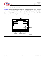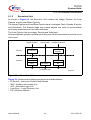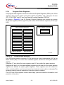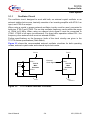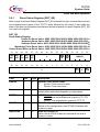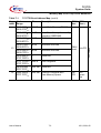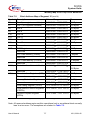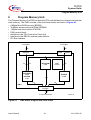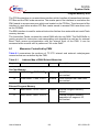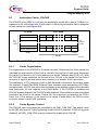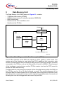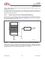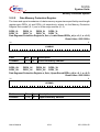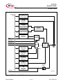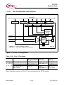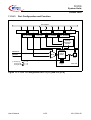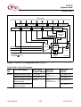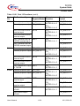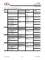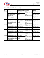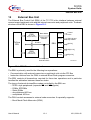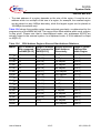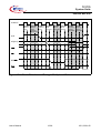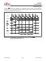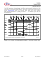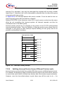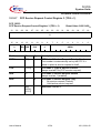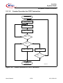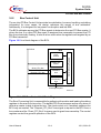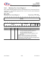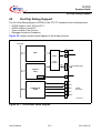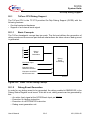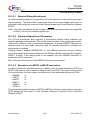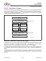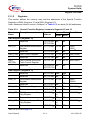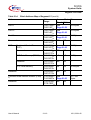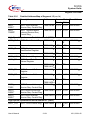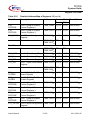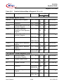
1
U s e r ’ s M a n u a l , V 2 .0 , F e b . 2 0 0 1 TC1775 System Units 32-Bit Single-Chip Microcontroller Microcontrollers N e v e r s t o p t h i n k i n g . Edition 2001-02 Published by Infineon Technologies AG, St.-Martin-Strasse 53, D-81541 München, Germany © Infineon Technologies AG 2001. All Rights Reserved. Attention please! The information herein is given to describe certain components and shall not be considered as warranted characteristics. Terms of delivery and rights to technical change reserved. We hereby disclaim any and all warranties, including but not limited to warranties of non-infringement, regarding circuits, descriptions and charts stated herein. Infineon Technologies is an approved CECC manufacturer. Information For further information on technology, delivery terms and conditions and prices please contact your nearest Infineon Technologies Office in Germany or our Infineon Technologies Representatives worldwide. Warnings Due to technical requirements components may contain dangerous substances. For information on the types in question please contact your nearest Infineon Technologies Office. Infineon Technologies Components may only be used in life-support devices or systems with the express written approval of Infineon Technologies, if a failure of such components can reasonably be expected to cause the failure of that life-support device or system, or to affect the safety or effectiveness of that device or system. Life support devices or systems are intended to be implanted in the human body, or to support and/or maintain and sustain and/or protect human life. If they fail, it is reasonable to assume that the health of the user or other persons may be endangered. U s e r ’ s M a n u a l , V 2 .0 , F e b . 2 0 0 1 TC1775 System Units 32-Bit Single-Chip Microcontroller Microcontrollers N e v e r s t o p t h i n k i n g . TC1775 System Units User’s Manual Revision History: 2001-02 Previous Version: Page V2.0 V1.0, 2000-11 (B-Step, PDF only)1) V1.1, 2000-05 (A-Step, PDF and limited print)2) V1.0, 2000-04 (A-Step, PDF only)2) Subjects (major changes since last revision) 1) This version is an intermediate version for the B-Step created for release purposes of the final version V2.0. 2) These versions for the A-Step have been created as an “Advance Information” for key customers and have not been published officially. We Listen to Your Comments Any information within this document that you feel is wrong, unclear or missing? Your feedback will help us to continuously improve the quality of this document. Please send your proposal (including a reference to this document) to: [email protected] TC1775 System Units Table of Contents 1 1.1 1.1.1 1.1.2 1.1.3 1.1.4 1.1.5 1.2 1.3 1.4 1.4.1 1.4.1.1 1.4.1.2 1.4.1.3 1.4.1.4 1.4.2 1.4.2.1 1.4.2.2 1.4.3 1.5 Page Introduction . . . . . . . . . . . . . . . . . . . . . . . . . . . . . . . . . . . . . . . . . . . . . . 1-1 About this Document . . . . . . . . . . . . . . . . . . . . . . . . . . . . . . . . . . . . . . . . 1-1 Related Documentations . . . . . . . . . . . . . . . . . . . . . . . . . . . . . . . . . . . 1-1 Textual Conventions . . . . . . . . . . . . . . . . . . . . . . . . . . . . . . . . . . . . . . 1-1 Reserved, Undefined, and Unimplemented Terminology . . . . . . . . . . 1-3 Register Access Modes . . . . . . . . . . . . . . . . . . . . . . . . . . . . . . . . . . . . 1-3 Abbreviations . . . . . . . . . . . . . . . . . . . . . . . . . . . . . . . . . . . . . . . . . . . . 1-4 System Architecture Features of the TC1775 . . . . . . . . . . . . . . . . . . . . . 1-6 Block Diagram . . . . . . . . . . . . . . . . . . . . . . . . . . . . . . . . . . . . . . . . . . . . . 1-9 On-Chip Peripheral Units of the TC1775 . . . . . . . . . . . . . . . . . . . . . . . . 1-10 Serial Interfaces . . . . . . . . . . . . . . . . . . . . . . . . . . . . . . . . . . . . . . . . . 1-11 Asynchronous/Synchronous Serial Interfaces . . . . . . . . . . . . . . . . 1-11 High-Speed Synchronous Serial Interfaces . . . . . . . . . . . . . . . . . . 1-13 TwinCAN Interface . . . . . . . . . . . . . . . . . . . . . . . . . . . . . . . . . . . . . 1-15 Serial Data Link Interface . . . . . . . . . . . . . . . . . . . . . . . . . . . . . . . 1-17 Timer Units . . . . . . . . . . . . . . . . . . . . . . . . . . . . . . . . . . . . . . . . . . . . 1-19 General Purpose Timer Unit . . . . . . . . . . . . . . . . . . . . . . . . . . . . . 1-19 General Purpose Timer Array . . . . . . . . . . . . . . . . . . . . . . . . . . . . 1-21 Analog-to-Digital Converters . . . . . . . . . . . . . . . . . . . . . . . . . . . . . . . 1-24 Pin Definitions and Functions . . . . . . . . . . . . . . . . . . . . . . . . . . . . . . . . 1-26 2 TC1775 Processor Architecture . . . . . . . . . . . . . . . . . . . . . . . . . . . . . . 2-1 2.1 Central Processing Unit . . . . . . . . . . . . . . . . . . . . . . . . . . . . . . . . . . . . . . 2-2 2.1.1 Instruction Fetch Unit . . . . . . . . . . . . . . . . . . . . . . . . . . . . . . . . . . . . . . 2-3 2.1.2 Execution Unit . . . . . . . . . . . . . . . . . . . . . . . . . . . . . . . . . . . . . . . . . . . 2-4 2.1.3 General Purpose Register File . . . . . . . . . . . . . . . . . . . . . . . . . . . . . . 2-5 2.1.4 Program State Registers . . . . . . . . . . . . . . . . . . . . . . . . . . . . . . . . . . . 2-6 2.1.5 Data Types . . . . . . . . . . . . . . . . . . . . . . . . . . . . . . . . . . . . . . . . . . . . . 2-7 2.1.6 Addressing Modes . . . . . . . . . . . . . . . . . . . . . . . . . . . . . . . . . . . . . . . . 2-7 2.1.7 Instruction Formats . . . . . . . . . . . . . . . . . . . . . . . . . . . . . . . . . . . . . . . 2-7 2.1.8 Tasks and Contexts . . . . . . . . . . . . . . . . . . . . . . . . . . . . . . . . . . . . . . . 2-7 2.1.8.1 Upper and Lower Contexts . . . . . . . . . . . . . . . . . . . . . . . . . . . . . . . 2-8 2.1.8.2 Context Save Areas . . . . . . . . . . . . . . . . . . . . . . . . . . . . . . . . . . . . . 2-9 2.1.8.3 Fast Context Switching . . . . . . . . . . . . . . . . . . . . . . . . . . . . . . . . . . 2-9 2.1.9 Interrupt System . . . . . . . . . . . . . . . . . . . . . . . . . . . . . . . . . . . . . . . . 2-10 2.1.10 Trap System . . . . . . . . . . . . . . . . . . . . . . . . . . . . . . . . . . . . . . . . . . . 2-10 2.1.11 Protection System . . . . . . . . . . . . . . . . . . . . . . . . . . . . . . . . . . . . . . . 2-11 2.1.11.1 Permission Levels . . . . . . . . . . . . . . . . . . . . . . . . . . . . . . . . . . . . . 2-11 2.1.11.2 Memory Protection Model . . . . . . . . . . . . . . . . . . . . . . . . . . . . . . . 2-11 2.1.11.3 Watchdog Timer and ENDINIT Protection . . . . . . . . . . . . . . . . . . . 2-12 2.1.12 Reset System . . . . . . . . . . . . . . . . . . . . . . . . . . . . . . . . . . . . . . . . . . 2-12 2.2 Processor Registers . . . . . . . . . . . . . . . . . . . . . . . . . . . . . . . . . . . . . . . 2-13 User’s Manual I-1 V2.0, 2001-02 TC1775 System Units Table of Contents 2.2.1 2.2.1.1 2.2.1.2 2.2.1.3 2.2.2 2.2.2.1 2.2.2.2 2.2.3 2.2.4 2.2.4.1 2.2.5 2.2.5.1 2.2.5.2 2.2.6 2.2.7 2.2.8 2.2.9 2.3 2.3.1 2.3.1.1 2.3.1.2 2.3.2 2.3.3 2.3.4 2.3.5 2.3.6 2.3.6.1 2.3.6.2 2.3.6.3 2.3.7 2.3.7.1 2.3.7.2 2.3.7.3 2.3.8 2.3.8.1 2.3.8.2 2.3.9 2.3.9.1 2.3.9.2 2.3.9.3 2.3.9.4 2.3.9.5 Page Program State Information Registers . . . . . . . . . . . . . . . . . . . . . . . . Program Counter (PC) . . . . . . . . . . . . . . . . . . . . . . . . . . . . . . . . . . Program Status Word (PSW) . . . . . . . . . . . . . . . . . . . . . . . . . . . . . Previous Context Information Register (PCXI) . . . . . . . . . . . . . . . Context Management Registers . . . . . . . . . . . . . . . . . . . . . . . . . . . . Free Context List Head Pointer (FCX) . . . . . . . . . . . . . . . . . . . . . . Previous Context Pointer (PCX) . . . . . . . . . . . . . . . . . . . . . . . . . . Free Context List Limit Pointer (LCX) . . . . . . . . . . . . . . . . . . . . . . . . Stack Management . . . . . . . . . . . . . . . . . . . . . . . . . . . . . . . . . . . . . . Interrupt Stack Pointer (ISP) . . . . . . . . . . . . . . . . . . . . . . . . . . . . . Interrupt and Trap Control . . . . . . . . . . . . . . . . . . . . . . . . . . . . . . . . . Interrupt Vector Table Pointer (BIV) . . . . . . . . . . . . . . . . . . . . . . . Trap Vector Table Pointer (BTV) . . . . . . . . . . . . . . . . . . . . . . . . . . System Control Register . . . . . . . . . . . . . . . . . . . . . . . . . . . . . . . . . . Memory Protection Registers . . . . . . . . . . . . . . . . . . . . . . . . . . . . . . Debug Registers . . . . . . . . . . . . . . . . . . . . . . . . . . . . . . . . . . . . . . . . CSFR Address Table . . . . . . . . . . . . . . . . . . . . . . . . . . . . . . . . . . . . . Instruction Set Overview . . . . . . . . . . . . . . . . . . . . . . . . . . . . . . . . . . . . Arithmetic Instructions . . . . . . . . . . . . . . . . . . . . . . . . . . . . . . . . . . . . Integer Arithmetic . . . . . . . . . . . . . . . . . . . . . . . . . . . . . . . . . . . . . . DSP Arithmetic . . . . . . . . . . . . . . . . . . . . . . . . . . . . . . . . . . . . . . . Compare Instructions . . . . . . . . . . . . . . . . . . . . . . . . . . . . . . . . . . . . . Bit Operations . . . . . . . . . . . . . . . . . . . . . . . . . . . . . . . . . . . . . . . . . . Address Arithmetic . . . . . . . . . . . . . . . . . . . . . . . . . . . . . . . . . . . . . . . Address Comparison . . . . . . . . . . . . . . . . . . . . . . . . . . . . . . . . . . . . . Branch Instructions . . . . . . . . . . . . . . . . . . . . . . . . . . . . . . . . . . . . . . Unconditional Branch . . . . . . . . . . . . . . . . . . . . . . . . . . . . . . . . . . . Conditional Branch . . . . . . . . . . . . . . . . . . . . . . . . . . . . . . . . . . . . Loop Instructions . . . . . . . . . . . . . . . . . . . . . . . . . . . . . . . . . . . . . . Load and Store Instructions . . . . . . . . . . . . . . . . . . . . . . . . . . . . . . . . Load/Store Basic Data Types . . . . . . . . . . . . . . . . . . . . . . . . . . . . Load Bit . . . . . . . . . . . . . . . . . . . . . . . . . . . . . . . . . . . . . . . . . . . . . Store Bit and Bit Field . . . . . . . . . . . . . . . . . . . . . . . . . . . . . . . . . . Context Related Instructions . . . . . . . . . . . . . . . . . . . . . . . . . . . . . . . Context Saving and Restoring . . . . . . . . . . . . . . . . . . . . . . . . . . . . Context Loading and Storing . . . . . . . . . . . . . . . . . . . . . . . . . . . . . System Instructions . . . . . . . . . . . . . . . . . . . . . . . . . . . . . . . . . . . . . . System Call . . . . . . . . . . . . . . . . . . . . . . . . . . . . . . . . . . . . . . . . . . Synchronization Primitives . . . . . . . . . . . . . . . . . . . . . . . . . . . . . . . Access to the Core Special Function Registers . . . . . . . . . . . . . . . Enabling/Disabling the Interrupt System . . . . . . . . . . . . . . . . . . . . RET and RFE . . . . . . . . . . . . . . . . . . . . . . . . . . . . . . . . . . . . . . . . User’s Manual I-2 2-16 2-16 2-17 2-21 2-23 2-23 2-24 2-25 2-26 2-26 2-27 2-27 2-28 2-29 2-30 2-30 2-31 2-34 2-34 2-35 2-42 2-46 2-50 2-52 2-53 2-54 2-54 2-55 2-56 2-57 2-57 2-59 2-59 2-60 2-60 2-60 2-61 2-61 2-61 2-62 2-62 2-63 V2.0, 2001-02 TC1775 System Units Table of Contents Page 2.3.9.6 2.3.9.7 2.3.10 2.4 2.4.1 2.4.2 2.4.3 2.4.4 Trap Instructions . . . . . . . . . . . . . . . . . . . . . . . . . . . . . . . . . . . . . . No Operation . . . . . . . . . . . . . . . . . . . . . . . . . . . . . . . . . . . . . . . . . 16-Bit Instructions . . . . . . . . . . . . . . . . . . . . . . . . . . . . . . . . . . . . . . . CPU Pipelines . . . . . . . . . . . . . . . . . . . . . . . . . . . . . . . . . . . . . . . . . . . . CPU Pipeline Overview . . . . . . . . . . . . . . . . . . . . . . . . . . . . . . . . . . . Integer and Load/Store Pipelines . . . . . . . . . . . . . . . . . . . . . . . . . . . Loop Pipeline . . . . . . . . . . . . . . . . . . . . . . . . . . . . . . . . . . . . . . . . . . . Context Operations . . . . . . . . . . . . . . . . . . . . . . . . . . . . . . . . . . . . . . 3 3.1 3.1.1 3.1.2 3.1.2.1 3.1.2.2 3.1.2.3 3.1.2.4 3.1.2.5 3.1.2.6 3.1.3 3.1.3.1 3.1.3.2 3.1.3.3 3.1.4 3.1.5 3.1.6 3.2 3.2.1 3.2.2 3.2.3 3.2.4 3.3 Clock System . . . . . . . . . . . . . . . . . . . . . . . . . . . . . . . . . . . . . . . . . . . . . 3-1 Clock Generation Unit . . . . . . . . . . . . . . . . . . . . . . . . . . . . . . . . . . . . . . . 3-3 Oscillator Circuit . . . . . . . . . . . . . . . . . . . . . . . . . . . . . . . . . . . . . . . . . . 3-4 Phase-Locked Loop (PLL) . . . . . . . . . . . . . . . . . . . . . . . . . . . . . . . . . . 3-5 N-Divider . . . . . . . . . . . . . . . . . . . . . . . . . . . . . . . . . . . . . . . . . . . . . 3-5 VCO Frequency Ranges . . . . . . . . . . . . . . . . . . . . . . . . . . . . . . . . . 3-5 Lock Detection . . . . . . . . . . . . . . . . . . . . . . . . . . . . . . . . . . . . . . . . . 3-5 K-Divider . . . . . . . . . . . . . . . . . . . . . . . . . . . . . . . . . . . . . . . . . . . . . 3-6 Clock Source Control . . . . . . . . . . . . . . . . . . . . . . . . . . . . . . . . . . . . 3-6 Enable/Disable Control . . . . . . . . . . . . . . . . . . . . . . . . . . . . . . . . . . 3-7 Determining the System Clock Frequency . . . . . . . . . . . . . . . . . . . . . 3-7 PLL Bypass Operation . . . . . . . . . . . . . . . . . . . . . . . . . . . . . . . . . . . 3-7 VCO Bypass Operation . . . . . . . . . . . . . . . . . . . . . . . . . . . . . . . . . . 3-8 PLL Operation . . . . . . . . . . . . . . . . . . . . . . . . . . . . . . . . . . . . . . . . . 3-8 PLL Clock Control and Status Register . . . . . . . . . . . . . . . . . . . . . . . 3-11 Startup Operation . . . . . . . . . . . . . . . . . . . . . . . . . . . . . . . . . . . . . . . 3-12 PLL Loss of Lock Operation . . . . . . . . . . . . . . . . . . . . . . . . . . . . . . . 3-13 Power Management and Clock Gating . . . . . . . . . . . . . . . . . . . . . . . . . 3-14 Clock Control . . . . . . . . . . . . . . . . . . . . . . . . . . . . . . . . . . . . . . . . . . . 3-15 Module Clock Generation . . . . . . . . . . . . . . . . . . . . . . . . . . . . . . . . . 3-16 Clock Control Registers . . . . . . . . . . . . . . . . . . . . . . . . . . . . . . . . . . . 3-17 CLC Register Implementations . . . . . . . . . . . . . . . . . . . . . . . . . . . . . 3-22 RTC Clock Generator . . . . . . . . . . . . . . . . . . . . . . . . . . . . . . . . . . . . . . 3-23 4 4.1 4.2 4.3 4.4 4.5 System Control Unit . . . . . . . . . . . . . . . . . . . . . . . . . . . . . . . . . . . . . . . Overview . . . . . . . . . . . . . . . . . . . . . . . . . . . . . . . . . . . . . . . . . . . . . . . . . Registers Overview . . . . . . . . . . . . . . . . . . . . . . . . . . . . . . . . . . . . . . . . . SCU Control Register . . . . . . . . . . . . . . . . . . . . . . . . . . . . . . . . . . . . . . . Port 5 Trace Control . . . . . . . . . . . . . . . . . . . . . . . . . . . . . . . . . . . . . . . . Identification Registers . . . . . . . . . . . . . . . . . . . . . . . . . . . . . . . . . . . . . . 5 5.1 5.2 Reset and Boot Operation . . . . . . . . . . . . . . . . . . . . . . . . . . . . . . . . . . 5-1 Overview . . . . . . . . . . . . . . . . . . . . . . . . . . . . . . . . . . . . . . . . . . . . . . . . . 5-1 Reset Registers . . . . . . . . . . . . . . . . . . . . . . . . . . . . . . . . . . . . . . . . . . . . 5-2 User’s Manual I-3 2-63 2-63 2-63 2-64 2-64 2-64 2-66 2-67 4-1 4-1 4-2 4-3 4-6 4-8 V2.0, 2001-02 TC1775 System Units Table of Contents Page 5.2.1 5.2.2 5.3 5.3.1 5.3.2 5.3.3 5.3.4 5.3.4.1 5.3.4.2 5.3.5 5.4 5.4.1 5.4.2 5.4.3 5.4.4 5.4.5 5.4.6 Reset Status Register (RST_SR) . . . . . . . . . . . . . . . . . . . . . . . . . . . . 5-3 Reset Request Register (RST_REQ) . . . . . . . . . . . . . . . . . . . . . . . . . 5-5 Reset Operations . . . . . . . . . . . . . . . . . . . . . . . . . . . . . . . . . . . . . . . . . . . 5-7 Power-On Reset . . . . . . . . . . . . . . . . . . . . . . . . . . . . . . . . . . . . . . . . . 5-7 External Hardware Reset . . . . . . . . . . . . . . . . . . . . . . . . . . . . . . . . . . . 5-7 Software Reset . . . . . . . . . . . . . . . . . . . . . . . . . . . . . . . . . . . . . . . . . . 5-8 Watchdog Timer Reset . . . . . . . . . . . . . . . . . . . . . . . . . . . . . . . . . . . . 5-9 Watchdog Timer Reset Lock . . . . . . . . . . . . . . . . . . . . . . . . . . . . . . 5-9 Deep-Sleep Wake-Up Reset . . . . . . . . . . . . . . . . . . . . . . . . . . . . . 5-10 State of the TC1775 after Reset . . . . . . . . . . . . . . . . . . . . . . . . . . . . 5-11 Booting Scheme . . . . . . . . . . . . . . . . . . . . . . . . . . . . . . . . . . . . . . . . . . 5-13 Hardware Booting Scheme . . . . . . . . . . . . . . . . . . . . . . . . . . . . . . . . 5-13 Software Booting Scheme . . . . . . . . . . . . . . . . . . . . . . . . . . . . . . . . . 5-13 Boot Options . . . . . . . . . . . . . . . . . . . . . . . . . . . . . . . . . . . . . . . . . . . 5-14 Boot Configuration Handling . . . . . . . . . . . . . . . . . . . . . . . . . . . . . . . 5-15 Normal Boot Options . . . . . . . . . . . . . . . . . . . . . . . . . . . . . . . . . . . . . 5-15 Debug Boot Options . . . . . . . . . . . . . . . . . . . . . . . . . . . . . . . . . . . . . 5-15 6 6.1 6.2 6.2.1 6.2.2 6.3 6.3.1 6.3.2 6.3.2.1 6.3.2.2 6.3.2.3 6.3.3 6.3.3.1 6.3.3.2 6.3.3.3 6.3.3.4 6.3.3.5 6.3.4 Power Management . . . . . . . . . . . . . . . . . . . . . . . . . . . . . . . . . . . . . . . . 6-1 Power Management Overview . . . . . . . . . . . . . . . . . . . . . . . . . . . . . . . . . 6-1 Power Management Control Registers . . . . . . . . . . . . . . . . . . . . . . . . . . 6-3 Power Management Control Register PMG_CON . . . . . . . . . . . . . . . 6-4 Power Management Control and Status Register PMG_CSR . . . . . . . 6-5 Power Management Modes . . . . . . . . . . . . . . . . . . . . . . . . . . . . . . . . . . . 6-6 Idle Mode . . . . . . . . . . . . . . . . . . . . . . . . . . . . . . . . . . . . . . . . . . . . . . . 6-6 Sleep Mode . . . . . . . . . . . . . . . . . . . . . . . . . . . . . . . . . . . . . . . . . . . . . 6-7 Entering Sleep Mode . . . . . . . . . . . . . . . . . . . . . . . . . . . . . . . . . . . . 6-7 TC1775 State During Sleep Mode . . . . . . . . . . . . . . . . . . . . . . . . . . 6-7 Exiting Sleep Mode . . . . . . . . . . . . . . . . . . . . . . . . . . . . . . . . . . . . . 6-7 Deep Sleep Mode . . . . . . . . . . . . . . . . . . . . . . . . . . . . . . . . . . . . . . . . 6-8 Entering Deep Sleep Mode . . . . . . . . . . . . . . . . . . . . . . . . . . . . . . . 6-8 TC1775 State During Deep Sleep Mode . . . . . . . . . . . . . . . . . . . . . 6-8 Exiting Deep Sleep Mode . . . . . . . . . . . . . . . . . . . . . . . . . . . . . . . . 6-9 Exiting Deep Sleep Mode With A Power-On Reset Signal . . . . . . . 6-9 Exiting Deep Sleep Mode With an NMI Signal . . . . . . . . . . . . . . . . 6-9 Summary of TC1775 Power Management States . . . . . . . . . . . . . . . 6-10 7 7.1 7.2 Memory Map of On-Chip Local Memories . . . . . . . . . . . . . . . . . . . . . . 7-1 TC1775 Address Map . . . . . . . . . . . . . . . . . . . . . . . . . . . . . . . . . . . . . . . 7-2 Memory Segment 15 - Peripheral Units . . . . . . . . . . . . . . . . . . . . . . . . . . 7-6 8 8.1 Program Memory Unit . . . . . . . . . . . . . . . . . . . . . . . . . . . . . . . . . . . . . . 8-1 Memories Controlled by PMU . . . . . . . . . . . . . . . . . . . . . . . . . . . . . . . . . 8-2 User’s Manual I-4 V2.0, 2001-02 TC1775 System Units Table of Contents Page 8.2 8.3 8.3.1 8.3.2 8.3.3 8.3.4 8.3.5 8.4 8.5 8.5.1 8.6 8.6.1 8.6.2 Scratch-Pad RAM, SPRAM . . . . . . . . . . . . . . . . . . . . . . . . . . . . . . . . . . . 8-3 Instruction Cache, ICACHE . . . . . . . . . . . . . . . . . . . . . . . . . . . . . . . . . . . 8-4 Cache Organization . . . . . . . . . . . . . . . . . . . . . . . . . . . . . . . . . . . . . . . 8-4 Cache Bypass Control . . . . . . . . . . . . . . . . . . . . . . . . . . . . . . . . . . . . . 8-4 Refill Buffer . . . . . . . . . . . . . . . . . . . . . . . . . . . . . . . . . . . . . . . . . . . . . 8-5 Refill Sequence for Cache and Refill Buffer . . . . . . . . . . . . . . . . . . . . 8-5 Cache Flush Operation . . . . . . . . . . . . . . . . . . . . . . . . . . . . . . . . . . . . 8-5 External Code Fetches via External Bus Interface Unit . . . . . . . . . . . . . . 8-6 Boot ROM . . . . . . . . . . . . . . . . . . . . . . . . . . . . . . . . . . . . . . . . . . . . . . . . 8-7 Bootstrap Loader Support . . . . . . . . . . . . . . . . . . . . . . . . . . . . . . . . . . 8-7 PMU Registers . . . . . . . . . . . . . . . . . . . . . . . . . . . . . . . . . . . . . . . . . . . . . 8-8 PMU Control Register . . . . . . . . . . . . . . . . . . . . . . . . . . . . . . . . . . . . . 8-9 External Instruction Fetch Control Register . . . . . . . . . . . . . . . . . . . . 8-11 9 9.1 9.1.1 9.1.2 9.1.3 9.1.4 9.2 9.2.1 9.2.2 9.2.3 9.2.4 9.3 9.3.1 9.3.2 9.3.3 9.3.4 Data Memory Unit . . . . . . . . . . . . . . . . . . . . . . . . . . . . . . . . . . . . . . . . . 9-1 DMU Trap Generation . . . . . . . . . . . . . . . . . . . . . . . . . . . . . . . . . . . . . . . 9-3 FPI Bus Error . . . . . . . . . . . . . . . . . . . . . . . . . . . . . . . . . . . . . . . . . . . . 9-3 Range Error . . . . . . . . . . . . . . . . . . . . . . . . . . . . . . . . . . . . . . . . . . . . . 9-4 DMU Register Access Error . . . . . . . . . . . . . . . . . . . . . . . . . . . . . . . . . 9-4 Cache Management Error . . . . . . . . . . . . . . . . . . . . . . . . . . . . . . . . . . 9-4 Overlay Functionality . . . . . . . . . . . . . . . . . . . . . . . . . . . . . . . . . . . . . . . . 9-5 Redirection From External Code to Internal Data Memory . . . . . . . . . 9-6 Redirection From External Code to External Data Memory . . . . . . . . . 9-7 Redirection From External Code via CODE to External Data Memory 9-8 Redirection From Ports to External Data Memory . . . . . . . . . . . . . . . . 9-9 DMU Registers . . . . . . . . . . . . . . . . . . . . . . . . . . . . . . . . . . . . . . . . . . . 9-10 Control Register . . . . . . . . . . . . . . . . . . . . . . . . . . . . . . . . . . . . . . . . . 9-11 Synchronous Trap Flag Register . . . . . . . . . . . . . . . . . . . . . . . . . . . . 9-12 Asynchronous Trap Flag Register . . . . . . . . . . . . . . . . . . . . . . . . . . . 9-13 Overlay Functionality Registers . . . . . . . . . . . . . . . . . . . . . . . . . . . . . 9-14 10 10.1 10.2 10.2.1 10.2.2 10.2.3 10.3 10.4 10.4.1 10.4.2 Memory Protection System . . . . . . . . . . . . . . . . . . . . . . . . . . . . . . . . 10-1 Memory Protection Overview . . . . . . . . . . . . . . . . . . . . . . . . . . . . . . . . . 10-1 Memory Protection Registers . . . . . . . . . . . . . . . . . . . . . . . . . . . . . . . . 10-3 PSW Protection Fields . . . . . . . . . . . . . . . . . . . . . . . . . . . . . . . . . . . . 10-7 Data Memory Protection Register . . . . . . . . . . . . . . . . . . . . . . . . . . 10-11 Code Memory Protection Register . . . . . . . . . . . . . . . . . . . . . . . . . . 10-14 Sample Protection Register Set . . . . . . . . . . . . . . . . . . . . . . . . . . . . . . 10-17 Memory Access Checking . . . . . . . . . . . . . . . . . . . . . . . . . . . . . . . . . . 10-18 Permitted versus Valid Accesses . . . . . . . . . . . . . . . . . . . . . . . . . . 10-18 Crossing Protection Boundaries . . . . . . . . . . . . . . . . . . . . . . . . . . . 10-19 User’s Manual I-5 V2.0, 2001-02 TC1775 System Units Table of Contents 11 11.1 11.2 11.2.1 11.2.2 11.2.3 11.2.4 11.2.5 11.2.6 11.2.7 11.2.8 11.2.8.1 11.2.8.2 11.3 11.3.1 11.3.2 11.3.3 11.4 11.4.1 11.4.2 11.4.3 11.5 11.5.1 11.5.2 11.5.3 11.6 11.6.1 11.6.2 11.6.3 11.7 11.7.1 11.7.2 11.7.3 11.8 11.8.1 11.8.2 11.8.3 11.9 11.9.1 11.9.2 11.10 11.10.1 Page Parallel Ports . . . . . . . . . . . . . . . . . . . . . . . . . . . . . . . . . . . . . . . . . . . . 11-1 General Port Operation . . . . . . . . . . . . . . . . . . . . . . . . . . . . . . . . . . . . . 11-2 Port Kernel Registers . . . . . . . . . . . . . . . . . . . . . . . . . . . . . . . . . . . . . . . 11-5 Data Output Register . . . . . . . . . . . . . . . . . . . . . . . . . . . . . . . . . . . . . 11-7 Data Input Register . . . . . . . . . . . . . . . . . . . . . . . . . . . . . . . . . . . . . . 11-8 Direction Register . . . . . . . . . . . . . . . . . . . . . . . . . . . . . . . . . . . . . . . 11-9 Open Drain Control Register . . . . . . . . . . . . . . . . . . . . . . . . . . . . . . 11-10 Input Configuration Register . . . . . . . . . . . . . . . . . . . . . . . . . . . . . . 11-11 Pull-Up/Pull-Down Device Control . . . . . . . . . . . . . . . . . . . . . . . . . . 11-12 Output Characteristics Control Register . . . . . . . . . . . . . . . . . . . . . 11-14 Alternate Port Functions . . . . . . . . . . . . . . . . . . . . . . . . . . . . . . . . . 11-17 Alternate Input Functions . . . . . . . . . . . . . . . . . . . . . . . . . . . . . . . 11-17 Alternate Output Functions . . . . . . . . . . . . . . . . . . . . . . . . . . . . . 11-17 Port 0 . . . . . . . . . . . . . . . . . . . . . . . . . . . . . . . . . . . . . . . . . . . . . . . . . . 11-18 Features . . . . . . . . . . . . . . . . . . . . . . . . . . . . . . . . . . . . . . . . . . . . . . 11-18 Registers . . . . . . . . . . . . . . . . . . . . . . . . . . . . . . . . . . . . . . . . . . . . . 11-18 Port Configuration and Function . . . . . . . . . . . . . . . . . . . . . . . . . . . 11-19 Port 1 . . . . . . . . . . . . . . . . . . . . . . . . . . . . . . . . . . . . . . . . . . . . . . . . . . 11-20 Features . . . . . . . . . . . . . . . . . . . . . . . . . . . . . . . . . . . . . . . . . . . . . . 11-20 Registers . . . . . . . . . . . . . . . . . . . . . . . . . . . . . . . . . . . . . . . . . . . . . 11-20 Port Configuration and Function . . . . . . . . . . . . . . . . . . . . . . . . . . . 11-21 Port 2 . . . . . . . . . . . . . . . . . . . . . . . . . . . . . . . . . . . . . . . . . . . . . . . . . . 11-22 Features . . . . . . . . . . . . . . . . . . . . . . . . . . . . . . . . . . . . . . . . . . . . . . 11-22 Registers . . . . . . . . . . . . . . . . . . . . . . . . . . . . . . . . . . . . . . . . . . . . . 11-22 Port Configuration and Function . . . . . . . . . . . . . . . . . . . . . . . . . . . 11-23 Port 3 . . . . . . . . . . . . . . . . . . . . . . . . . . . . . . . . . . . . . . . . . . . . . . . . . . 11-24 Features . . . . . . . . . . . . . . . . . . . . . . . . . . . . . . . . . . . . . . . . . . . . . . 11-24 Registers . . . . . . . . . . . . . . . . . . . . . . . . . . . . . . . . . . . . . . . . . . . . . 11-24 Port Configuration and Function . . . . . . . . . . . . . . . . . . . . . . . . . . . 11-25 Port 4 . . . . . . . . . . . . . . . . . . . . . . . . . . . . . . . . . . . . . . . . . . . . . . . . . . 11-31 Features . . . . . . . . . . . . . . . . . . . . . . . . . . . . . . . . . . . . . . . . . . . . . . 11-31 Registers . . . . . . . . . . . . . . . . . . . . . . . . . . . . . . . . . . . . . . . . . . . . . 11-31 Port Configuration and Function . . . . . . . . . . . . . . . . . . . . . . . . . . . 11-32 Port 5 . . . . . . . . . . . . . . . . . . . . . . . . . . . . . . . . . . . . . . . . . . . . . . . . . . 11-35 Features . . . . . . . . . . . . . . . . . . . . . . . . . . . . . . . . . . . . . . . . . . . . . . 11-35 Registers . . . . . . . . . . . . . . . . . . . . . . . . . . . . . . . . . . . . . . . . . . . . . 11-35 Port Configuration and Function . . . . . . . . . . . . . . . . . . . . . . . . . . . 11-36 Port 6 . . . . . . . . . . . . . . . . . . . . . . . . . . . . . . . . . . . . . . . . . . . . . . . . . . 11-37 Features . . . . . . . . . . . . . . . . . . . . . . . . . . . . . . . . . . . . . . . . . . . . . . 11-37 Port 6 Functions . . . . . . . . . . . . . . . . . . . . . . . . . . . . . . . . . . . . . . . . 11-37 Port 7 . . . . . . . . . . . . . . . . . . . . . . . . . . . . . . . . . . . . . . . . . . . . . . . . . . 11-38 Features . . . . . . . . . . . . . . . . . . . . . . . . . . . . . . . . . . . . . . . . . . . . . . 11-38 User’s Manual I-6 V2.0, 2001-02 TC1775 System Units Table of Contents Page 11.10.2 11.11 11.11.1 11.11.2 11.11.3 11.12 11.12.1 11.12.2 11.12.3 11.13 11.13.1 11.13.2 11.13.3 11.14 11.14.1 11.14.2 11.14.3 11.15 11.15.1 11.15.2 11.15.3 11.16 11.16.1 11.16.2 11.16.3 Port 7 Functions . . . . . . . . . . . . . . . . . . . . . . . . . . . . . . . . . . . . . . . . Port 8 . . . . . . . . . . . . . . . . . . . . . . . . . . . . . . . . . . . . . . . . . . . . . . . . . . Features . . . . . . . . . . . . . . . . . . . . . . . . . . . . . . . . . . . . . . . . . . . . . . Registers . . . . . . . . . . . . . . . . . . . . . . . . . . . . . . . . . . . . . . . . . . . . . Port Configuration and Function . . . . . . . . . . . . . . . . . . . . . . . . . . . Port 9 . . . . . . . . . . . . . . . . . . . . . . . . . . . . . . . . . . . . . . . . . . . . . . . . . . Features . . . . . . . . . . . . . . . . . . . . . . . . . . . . . . . . . . . . . . . . . . . . . . Registers . . . . . . . . . . . . . . . . . . . . . . . . . . . . . . . . . . . . . . . . . . . . . Port Configuration and Function . . . . . . . . . . . . . . . . . . . . . . . . . . . Port 10 . . . . . . . . . . . . . . . . . . . . . . . . . . . . . . . . . . . . . . . . . . . . . . . . . Features . . . . . . . . . . . . . . . . . . . . . . . . . . . . . . . . . . . . . . . . . . . . . . Registers . . . . . . . . . . . . . . . . . . . . . . . . . . . . . . . . . . . . . . . . . . . . . Port Configuration and Function . . . . . . . . . . . . . . . . . . . . . . . . . . . Port 11 . . . . . . . . . . . . . . . . . . . . . . . . . . . . . . . . . . . . . . . . . . . . . . . . . Features . . . . . . . . . . . . . . . . . . . . . . . . . . . . . . . . . . . . . . . . . . . . . . Registers . . . . . . . . . . . . . . . . . . . . . . . . . . . . . . . . . . . . . . . . . . . . . Port Configuration and Function . . . . . . . . . . . . . . . . . . . . . . . . . . . Port 12 . . . . . . . . . . . . . . . . . . . . . . . . . . . . . . . . . . . . . . . . . . . . . . . . . Features . . . . . . . . . . . . . . . . . . . . . . . . . . . . . . . . . . . . . . . . . . . . . . Registers . . . . . . . . . . . . . . . . . . . . . . . . . . . . . . . . . . . . . . . . . . . . . Port Configuration and Function . . . . . . . . . . . . . . . . . . . . . . . . . . . Port 13 . . . . . . . . . . . . . . . . . . . . . . . . . . . . . . . . . . . . . . . . . . . . . . . . . Features . . . . . . . . . . . . . . . . . . . . . . . . . . . . . . . . . . . . . . . . . . . . . . Registers . . . . . . . . . . . . . . . . . . . . . . . . . . . . . . . . . . . . . . . . . . . . . Port Configuration and Function . . . . . . . . . . . . . . . . . . . . . . . . . . . 11-38 11-39 11-39 11-39 11-40 11-41 11-41 11-41 11-42 11-43 11-43 11-43 11-44 11-45 11-45 11-45 11-46 11-47 11-47 11-47 11-48 11-52 11-52 11-52 11-53 12 12.1 12.2 12.3 12.3.1 12.3.2 12.4 12.4.1 12.4.2 12.4.3 12.4.4 12.4.5 12.4.6 12.4.7 12.4.8 12.4.9 External Bus Unit . . . . . . . . . . . . . . . . . . . . . . . . . . . . . . . . . . . . . . . . . 12-1 Overview . . . . . . . . . . . . . . . . . . . . . . . . . . . . . . . . . . . . . . . . . . . . . . . . 12-2 EBU Features . . . . . . . . . . . . . . . . . . . . . . . . . . . . . . . . . . . . . . . . . . . . 12-3 Basic EBU Operation . . . . . . . . . . . . . . . . . . . . . . . . . . . . . . . . . . . . . . . 12-4 Internal to External Operation . . . . . . . . . . . . . . . . . . . . . . . . . . . . . . 12-6 External to Internal Operation . . . . . . . . . . . . . . . . . . . . . . . . . . . . . . 12-6 EBU Signal Description . . . . . . . . . . . . . . . . . . . . . . . . . . . . . . . . . . . . . 12-7 Output Clock, CLKOUT . . . . . . . . . . . . . . . . . . . . . . . . . . . . . . . . . . . 12-8 Address Bus, A[25:0] . . . . . . . . . . . . . . . . . . . . . . . . . . . . . . . . . . . . . 12-8 Address/Data Bus, AD[31:0] . . . . . . . . . . . . . . . . . . . . . . . . . . . . . . . 12-8 Read/Write Strobes, RD and RD/WR . . . . . . . . . . . . . . . . . . . . . . . . 12-8 Address Latch Enable, ALE . . . . . . . . . . . . . . . . . . . . . . . . . . . . . . . . 12-9 Byte Control Signals, BCx . . . . . . . . . . . . . . . . . . . . . . . . . . . . . . . . . 12-9 Variable Wait State Control, WAIT . . . . . . . . . . . . . . . . . . . . . . . . . 12-10 Chip Select Lines, CSx . . . . . . . . . . . . . . . . . . . . . . . . . . . . . . . . . . 12-11 EBU Arbitration Signals, HOLD, HLDA and BREQ . . . . . . . . . . . . . 12-11 User’s Manual I-7 V2.0, 2001-02 TC1775 System Units Table of Contents 12.4.10 12.4.11 12.4.12 12.5 12.5.1 12.5.1.1 12.5.1.2 12.5.2 12.5.3 12.5.4 12.5.4.1 12.5.4.2 12.6 12.6.1 12.6.2 12.6.3 12.6.4 12.7 12.7.1 12.7.1.1 12.7.1.2 12.7.1.3 12.7.2 12.7.3 12.7.4 12.7.4.1 12.7.4.2 12.8 12.9 12.9.1 12.9.2 12.10 12.10.1 12.10.2 12.10.3 12.10.4 12.10.5 12.10.6 12.11 12.11.1 12.11.2 12.11.3 Page EBU Chip Select, CSFPI . . . . . . . . . . . . . . . . . . . . . . . . . . . . . . . . . Instruction Fetch Indication Signal, CODE . . . . . . . . . . . . . . . . . . . Emulation Support Signals, CSEMU and CSOVL . . . . . . . . . . . . . . Detailed Internal to External EBU Operation . . . . . . . . . . . . . . . . . . . . EBU Address Regions . . . . . . . . . . . . . . . . . . . . . . . . . . . . . . . . . . . Address Region Selection . . . . . . . . . . . . . . . . . . . . . . . . . . . . . . Address Region Parameters . . . . . . . . . . . . . . . . . . . . . . . . . . . . Driver Turn-Around Wait States . . . . . . . . . . . . . . . . . . . . . . . . . . . . Data Width of External Devices . . . . . . . . . . . . . . . . . . . . . . . . . . . . Basic Access Timing . . . . . . . . . . . . . . . . . . . . . . . . . . . . . . . . . . . . Access to Non-Multiplexed Devices . . . . . . . . . . . . . . . . . . . . . . Access to Multiplexed Devices . . . . . . . . . . . . . . . . . . . . . . . . . . Detailed External to Internal EBU Operation . . . . . . . . . . . . . . . . . . . . EBU Signal Direction . . . . . . . . . . . . . . . . . . . . . . . . . . . . . . . . . . . . Address Translation . . . . . . . . . . . . . . . . . . . . . . . . . . . . . . . . . . . . . External to Internal Access Controls . . . . . . . . . . . . . . . . . . . . . . . . Basic Access Timing . . . . . . . . . . . . . . . . . . . . . . . . . . . . . . . . . . . . Arbitration . . . . . . . . . . . . . . . . . . . . . . . . . . . . . . . . . . . . . . . . . . . . . . External Bus Arbitration . . . . . . . . . . . . . . . . . . . . . . . . . . . . . . . . . . Arbitration Modes . . . . . . . . . . . . . . . . . . . . . . . . . . . . . . . . . . . . . Arbitration Signals . . . . . . . . . . . . . . . . . . . . . . . . . . . . . . . . . . . . Arbitration Sequence . . . . . . . . . . . . . . . . . . . . . . . . . . . . . . . . . . Internal Request to the EBU . . . . . . . . . . . . . . . . . . . . . . . . . . . . . . External Requests to the EBU . . . . . . . . . . . . . . . . . . . . . . . . . . . . . Atomic Read-Modify-Write Accesses . . . . . . . . . . . . . . . . . . . . . . . Internal to External Read-Modify-Write Access . . . . . . . . . . . . . . External to Internal Read-Modify-Write Access . . . . . . . . . . . . . . EBU Boot Process . . . . . . . . . . . . . . . . . . . . . . . . . . . . . . . . . . . . . . . . Emulation Support . . . . . . . . . . . . . . . . . . . . . . . . . . . . . . . . . . . . . . . . Emulation Boot . . . . . . . . . . . . . . . . . . . . . . . . . . . . . . . . . . . . . . . . Overlay Memory . . . . . . . . . . . . . . . . . . . . . . . . . . . . . . . . . . . . . . . External Instruction Fetches . . . . . . . . . . . . . . . . . . . . . . . . . . . . . . . . Signal List . . . . . . . . . . . . . . . . . . . . . . . . . . . . . . . . . . . . . . . . . . . . Basic Functions . . . . . . . . . . . . . . . . . . . . . . . . . . . . . . . . . . . . . . . . External Instruction Fetch Control Register . . . . . . . . . . . . . . . . . . . Cycle Definitions of Burst Mode Timing . . . . . . . . . . . . . . . . . . . . . . Typical Burst Flash Memory Configuration . . . . . . . . . . . . . . . . . . . Arbitration between EBU and PMU for External Accesses . . . . . . . EBU Registers . . . . . . . . . . . . . . . . . . . . . . . . . . . . . . . . . . . . . . . . . . . Clock Control Register . . . . . . . . . . . . . . . . . . . . . . . . . . . . . . . . . . . Global Control Register . . . . . . . . . . . . . . . . . . . . . . . . . . . . . . . . . . Address Select Registers . . . . . . . . . . . . . . . . . . . . . . . . . . . . . . . . User’s Manual I-8 12-12 12-12 12-12 12-13 12-13 12-13 12-16 12-17 12-18 12-21 12-21 12-25 12-29 12-29 12-30 12-32 12-32 12-34 12-35 12-36 12-36 12-38 12-39 12-40 12-41 12-41 12-41 12-42 12-45 12-45 12-45 12-47 12-47 12-47 12-48 12-50 12-56 12-56 12-57 12-58 12-59 12-61 V2.0, 2001-02 TC1775 System Units Table of Contents Page 12.11.4 12.11.5 12.11.6 12.11.7 12.11.8 12.11.9 12-62 12-65 12-66 12-69 12-70 12-71 Bus Configuration Registers . . . . . . . . . . . . . . . . . . . . . . . . . . . . . . Emulator Configuration Register . . . . . . . . . . . . . . . . . . . . . . . . . . . Emulator Bus Configuration Register . . . . . . . . . . . . . . . . . . . . . . . Emulator Address Select Register . . . . . . . . . . . . . . . . . . . . . . . . . . External Access Configuration Register . . . . . . . . . . . . . . . . . . . . . EBU Register Address Range . . . . . . . . . . . . . . . . . . . . . . . . . . . . . 13 13.1 13.2 13.3 13.3.1 13.3.1.1 13.3.1.2 13.3.1.3 13.3.1.4 13.3.1.5 13.3.1.6 13.4 13.4.1 13.4.1.1 13.4.1.2 13.4.2 13.5 13.5.1 13.5.2 13.6 13.7 13.8 13.9 13.9.1 13.9.2 13.9.3 13.9.4 13.9.5 13.9.6 13.9.7 13.10 13.11 Interrupt System . . . . . . . . . . . . . . . . . . . . . . . . . . . . . . . . . . . . . . . . . 13-1 Overview . . . . . . . . . . . . . . . . . . . . . . . . . . . . . . . . . . . . . . . . . . . . . . . . 13-2 External Interrupts . . . . . . . . . . . . . . . . . . . . . . . . . . . . . . . . . . . . . . . . . 13-4 Service Request Nodes . . . . . . . . . . . . . . . . . . . . . . . . . . . . . . . . . . . . . 13-4 Service Request Control Registers . . . . . . . . . . . . . . . . . . . . . . . . . . 13-4 Service Request Flag (SRR) . . . . . . . . . . . . . . . . . . . . . . . . . . . . . 13-6 Request Set and Clear Bits (SETR, CLRR) . . . . . . . . . . . . . . . . . . 13-6 Enable Bit (SRE) . . . . . . . . . . . . . . . . . . . . . . . . . . . . . . . . . . . . . . 13-6 Service Request Flag (SRR) . . . . . . . . . . . . . . . . . . . . . . . . . . . . . 13-7 Type-of-Service Control (TOS) . . . . . . . . . . . . . . . . . . . . . . . . . . . 13-7 Service Request Priority Number (SRPN) . . . . . . . . . . . . . . . . . . . 13-7 Interrupt Control Units . . . . . . . . . . . . . . . . . . . . . . . . . . . . . . . . . . . . . . 13-9 Interrupt Control Unit (ICU) . . . . . . . . . . . . . . . . . . . . . . . . . . . . . . . . 13-9 ICU Interrupt Control Register (ICR) . . . . . . . . . . . . . . . . . . . . . . . 13-9 Operation of the Interrupt Control Unit (ICU) . . . . . . . . . . . . . . . . 13-11 PCP Interrupt Control Unit (PICU) . . . . . . . . . . . . . . . . . . . . . . . . . . 13-12 Arbitration Process . . . . . . . . . . . . . . . . . . . . . . . . . . . . . . . . . . . . . . . 13-13 Controlling the Number of Arbitration Cycles . . . . . . . . . . . . . . . . . . 13-13 Controlling the Duration of Arbitration Cycles . . . . . . . . . . . . . . . . . 13-14 Entering an Interrupt Service Routine . . . . . . . . . . . . . . . . . . . . . . . . . 13-14 Exiting an Interrupt Service Routine . . . . . . . . . . . . . . . . . . . . . . . . . . 13-15 Interrupt Vector Table . . . . . . . . . . . . . . . . . . . . . . . . . . . . . . . . . . . . . 13-16 Usage of the TC1775 Interrupt System . . . . . . . . . . . . . . . . . . . . . . . . 13-19 Spanning Interrupt Service Routines Across Vector Entries . . . . . . 13-19 Configuring Ordinary Interrupt Service Routines . . . . . . . . . . . . . . . 13-20 Interrupt Priority Groups . . . . . . . . . . . . . . . . . . . . . . . . . . . . . . . . . 13-20 Splitting Interrupt Service Across Different Priority Levels . . . . . . . 13-21 Using different Priorities for the same Interrupt Source . . . . . . . . . . 13-22 Software Initiated Interrupts . . . . . . . . . . . . . . . . . . . . . . . . . . . . . . . 13-23 Interrupt Priority 1 . . . . . . . . . . . . . . . . . . . . . . . . . . . . . . . . . . . . . . 13-23 CPU Service Request Nodes . . . . . . . . . . . . . . . . . . . . . . . . . . . . . . . 13-24 Service Request Register Table . . . . . . . . . . . . . . . . . . . . . . . . . . . . . 13-26 14 14.1 Trap System . . . . . . . . . . . . . . . . . . . . . . . . . . . . . . . . . . . . . . . . . . . . . 14-1 Trap System Overview . . . . . . . . . . . . . . . . . . . . . . . . . . . . . . . . . . . . . 14-1 User’s Manual I-9 V2.0, 2001-02 TC1775 System Units Table of Contents Page 14.2 14.2.1 14.2.2 14.2.3 14.2.4 14.2.5 14.3 14.3.1 14.4 14.4.1 14.4.2 14.4.3 14.4.4 Trap Classes . . . . . . . . . . . . . . . . . . . . . . . . . . . . . . . . . . . . . . . . . . . . . 14-3 Synchronous Traps . . . . . . . . . . . . . . . . . . . . . . . . . . . . . . . . . . . . . . 14-5 Asynchronous Traps . . . . . . . . . . . . . . . . . . . . . . . . . . . . . . . . . . . . . 14-5 Hardware Traps . . . . . . . . . . . . . . . . . . . . . . . . . . . . . . . . . . . . . . . . . 14-5 Software Traps . . . . . . . . . . . . . . . . . . . . . . . . . . . . . . . . . . . . . . . . . 14-5 Trap Descriptions . . . . . . . . . . . . . . . . . . . . . . . . . . . . . . . . . . . . . . . . 14-6 Trap Vector Table . . . . . . . . . . . . . . . . . . . . . . . . . . . . . . . . . . . . . . . . 14-10 Entering a Trap Service Routine . . . . . . . . . . . . . . . . . . . . . . . . . . . 14-11 Non-Maskable Interrupt . . . . . . . . . . . . . . . . . . . . . . . . . . . . . . . . . . . . 14-12 NMI Status Register . . . . . . . . . . . . . . . . . . . . . . . . . . . . . . . . . . . . . 14-12 External NMI Input . . . . . . . . . . . . . . . . . . . . . . . . . . . . . . . . . . . . . . 14-13 Phase-Locked Loop NMI . . . . . . . . . . . . . . . . . . . . . . . . . . . . . . . . . 14-13 Watchdog Timer NMI . . . . . . . . . . . . . . . . . . . . . . . . . . . . . . . . . . . . 14-14 15 15.1 15.2 15.2.1 15.2.2 15.2.3 15.2.4 15.2.5 15.3 15.3.1 15.3.1.1 15.3.1.2 15.3.1.3 15.3.1.4 15.3.1.5 15.3.2 15.3.2.1 15.3.2.2 15.3.2.3 15.3.2.4 15.3.3 15.3.3.1 15.3.3.2 15.4 15.4.1 15.4.2 15.4.3 15.4.3.1 Peripheral Control Processor . . . . . . . . . . . . . . . . . . . . . . . . . . . . . . . 15-1 Peripheral Control Processor Overview . . . . . . . . . . . . . . . . . . . . . . . . . 15-1 PCP Architecture . . . . . . . . . . . . . . . . . . . . . . . . . . . . . . . . . . . . . . . . . . 15-2 PCP Processor . . . . . . . . . . . . . . . . . . . . . . . . . . . . . . . . . . . . . . . . . 15-3 PCP Code Memory . . . . . . . . . . . . . . . . . . . . . . . . . . . . . . . . . . . . . . 15-4 PCP Parameter RAM . . . . . . . . . . . . . . . . . . . . . . . . . . . . . . . . . . . . . 15-4 FPI Bus Interface . . . . . . . . . . . . . . . . . . . . . . . . . . . . . . . . . . . . . . . . 15-4 PCP Interrupt Control Unit and Service Request Nodes . . . . . . . . . . 15-5 PCP Programming Model . . . . . . . . . . . . . . . . . . . . . . . . . . . . . . . . . . . 15-6 General Purpose Register Set of the PCP . . . . . . . . . . . . . . . . . . . . 15-6 Register R0 . . . . . . . . . . . . . . . . . . . . . . . . . . . . . . . . . . . . . . . . . . 15-7 Registers R1, R2, and R3 . . . . . . . . . . . . . . . . . . . . . . . . . . . . . . . 15-7 Registers R4 and R5 . . . . . . . . . . . . . . . . . . . . . . . . . . . . . . . . . . . 15-7 Register R6 . . . . . . . . . . . . . . . . . . . . . . . . . . . . . . . . . . . . . . . . . . 15-7 Register R7 . . . . . . . . . . . . . . . . . . . . . . . . . . . . . . . . . . . . . . . . . . 15-8 Contexts and Context Models . . . . . . . . . . . . . . . . . . . . . . . . . . . . . 15-10 Context Models . . . . . . . . . . . . . . . . . . . . . . . . . . . . . . . . . . . . . . 15-10 Context Save Area . . . . . . . . . . . . . . . . . . . . . . . . . . . . . . . . . . . . 15-13 Context Save and Restore Operation for CR6 and CR7 . . . . . . . 15-16 Initialization of the Contexts . . . . . . . . . . . . . . . . . . . . . . . . . . . . . 15-17 Channel Programs . . . . . . . . . . . . . . . . . . . . . . . . . . . . . . . . . . . . . . 15-18 Channel Restart Mode . . . . . . . . . . . . . . . . . . . . . . . . . . . . . . . . . 15-18 Channel Resume Mode . . . . . . . . . . . . . . . . . . . . . . . . . . . . . . . . 15-19 PCP Operation . . . . . . . . . . . . . . . . . . . . . . . . . . . . . . . . . . . . . . . . . . . 15-21 PCP Initialization . . . . . . . . . . . . . . . . . . . . . . . . . . . . . . . . . . . . . . . 15-21 Channel Invocation and Context Restore Operation . . . . . . . . . . . . 15-21 Channel Exit and Context Save Operation . . . . . . . . . . . . . . . . . . . 15-22 Normal Exit . . . . . . . . . . . . . . . . . . . . . . . . . . . . . . . . . . . . . . . . . 15-22 User’s Manual I-10 V2.0, 2001-02 TC1775 System Units Table of Contents Page 15.4.3.2 Error Condition Channel Exit . . . . . . . . . . . . . . . . . . . . . . . . . . . . 15.4.3.3 Debug Exit . . . . . . . . . . . . . . . . . . . . . . . . . . . . . . . . . . . . . . . . . . 15.5 PCP Interrupt Operation . . . . . . . . . . . . . . . . . . . . . . . . . . . . . . . . . . . 15.5.1 Issuing Service Requests to CPU or PCP . . . . . . . . . . . . . . . . . . . . 15.5.2 PCP Interrupt Control Unit . . . . . . . . . . . . . . . . . . . . . . . . . . . . . . . . 15.5.3 PCP Service Request Nodes . . . . . . . . . . . . . . . . . . . . . . . . . . . . . . 15.5.4 Issuing PCP Service Requests . . . . . . . . . . . . . . . . . . . . . . . . . . . . 15.5.4.1 Service Request on EXIT Instruction . . . . . . . . . . . . . . . . . . . . . . 15.5.4.2 Service Request on Error . . . . . . . . . . . . . . . . . . . . . . . . . . . . . . 15.5.4.3 Queue Full Operation . . . . . . . . . . . . . . . . . . . . . . . . . . . . . . . . . 15.6 PCP Error Handling . . . . . . . . . . . . . . . . . . . . . . . . . . . . . . . . . . . . . . . 15.6.1 Enforced PRAM Partitioning . . . . . . . . . . . . . . . . . . . . . . . . . . . . . . 15.6.2 Channel Watchdog . . . . . . . . . . . . . . . . . . . . . . . . . . . . . . . . . . . . . 15.6.3 Invalid Opcode . . . . . . . . . . . . . . . . . . . . . . . . . . . . . . . . . . . . . . . . . 15.6.4 Instruction Address Error . . . . . . . . . . . . . . . . . . . . . . . . . . . . . . . . . 15.7 Instruction Set Overview . . . . . . . . . . . . . . . . . . . . . . . . . . . . . . . . . . . 15.7.1 DMA Primitives . . . . . . . . . . . . . . . . . . . . . . . . . . . . . . . . . . . . . . . . 15.7.2 Load and Store . . . . . . . . . . . . . . . . . . . . . . . . . . . . . . . . . . . . . . . . 15.7.3 Arithmetic and Logical Instructions . . . . . . . . . . . . . . . . . . . . . . . . . 15.7.4 Bit Manipulation . . . . . . . . . . . . . . . . . . . . . . . . . . . . . . . . . . . . . . . . 15.7.5 Flow Control . . . . . . . . . . . . . . . . . . . . . . . . . . . . . . . . . . . . . . . . . . . 15.7.6 Addressing Modes . . . . . . . . . . . . . . . . . . . . . . . . . . . . . . . . . . . . . . 15.7.6.1 FPI Bus Addressing . . . . . . . . . . . . . . . . . . . . . . . . . . . . . . . . . . . 15.7.6.2 PRAM Addressing . . . . . . . . . . . . . . . . . . . . . . . . . . . . . . . . . . . . 15.7.6.3 Bit Addressing . . . . . . . . . . . . . . . . . . . . . . . . . . . . . . . . . . . . . . . 15.7.6.4 Flow Control Destination Addressing . . . . . . . . . . . . . . . . . . . . . . 15.8 Accessing PCP Resources from the FPI Bus . . . . . . . . . . . . . . . . . . . 15.8.1 Access to the PCP Control Registers . . . . . . . . . . . . . . . . . . . . . . . 15.8.2 Access to the PRAM . . . . . . . . . . . . . . . . . . . . . . . . . . . . . . . . . . . . 15.8.3 Access to the PCODE . . . . . . . . . . . . . . . . . . . . . . . . . . . . . . . . . . . 15.9 Debugging the PCP . . . . . . . . . . . . . . . . . . . . . . . . . . . . . . . . . . . . . . . 15.10 PCP Registers . . . . . . . . . . . . . . . . . . . . . . . . . . . . . . . . . . . . . . . . . . . 15.10.1 PCP Control and Status Register, PCP_CS . . . . . . . . . . . . . . . . . . 15.10.2 PCP Error/Debug Status Register, PCP_ES . . . . . . . . . . . . . . . . . . 15.10.3 PCP Interrupt Control Register, PCP_ICR . . . . . . . . . . . . . . . . . . . 15.10.4 PCP Service Request Control Register 0 (TOS = 0) . . . . . . . . . . . . 15.10.5 PCP Service Request Control Register 1 (TOS = 0) . . . . . . . . . . . . 15.10.6 PCP Service Request Control Register 2 (TOS = 1) . . . . . . . . . . . . 15.10.7 PCP Service Request Control Register 3 (TOS = 1) . . . . . . . . . . . . 15.11 PCP Instruction Set Details . . . . . . . . . . . . . . . . . . . . . . . . . . . . . . . . . 15.11.1 Instruction Codes and Fields . . . . . . . . . . . . . . . . . . . . . . . . . . . . . . 15.11.1.1 Conditional Codes . . . . . . . . . . . . . . . . . . . . . . . . . . . . . . . . . . . . 15-23 15-24 15-25 15-25 15-26 15-26 15-27 15-27 15-28 15-28 15-30 15-30 15-31 15-31 15-31 15-32 15-32 15-33 15-34 15-36 15-36 15-37 15-37 15-38 15-38 15-38 15-40 15-40 15-40 15-41 15-42 15-43 15-44 15-47 15-49 15-51 15-52 15-53 15-54 15-55 15-55 15-56 User’s Manual I-11 V2.0, 2001-02 TC1775 System Units Table of Contents Page 15.11.1.2 Instruction Fields . . . . . . . . . . . . . . . . . . . . . . . . . . . . . . . . . . . . . 15.11.2 Counter Operation for COPY Instruction . . . . . . . . . . . . . . . . . . . . . 15.11.3 Divide and Multiply Instructions . . . . . . . . . . . . . . . . . . . . . . . . . . . . 15.11.4 ADD, 32-Bit Addition . . . . . . . . . . . . . . . . . . . . . . . . . . . . . . . . . . . . 15.11.5 AND, 32-Bit Logical AND . . . . . . . . . . . . . . . . . . . . . . . . . . . . . . . . . 15.11.6 CHKB, Check Bit . . . . . . . . . . . . . . . . . . . . . . . . . . . . . . . . . . . . . . . 15.11.7 CLR, Clear Bit . . . . . . . . . . . . . . . . . . . . . . . . . . . . . . . . . . . . . . . . . 15.11.8 COMP, 32-Bit Compare . . . . . . . . . . . . . . . . . . . . . . . . . . . . . . . . . . 15.11.9 COPY, DMA Instruction . . . . . . . . . . . . . . . . . . . . . . . . . . . . . . . . . . 15.11.10 DEBUG, Debug Instruction . . . . . . . . . . . . . . . . . . . . . . . . . . . . . . . 15.11.11 DINIT, Divide Initialization Instruction . . . . . . . . . . . . . . . . . . . . . . . 15.11.12 DSTEP, Divide Instruction . . . . . . . . . . . . . . . . . . . . . . . . . . . . . . . . 15.11.13 INB, Insert Bit . . . . . . . . . . . . . . . . . . . . . . . . . . . . . . . . . . . . . . . . . . 15.11.14 EXIT, Exit Instruction . . . . . . . . . . . . . . . . . . . . . . . . . . . . . . . . . . . . 15.11.15 JC, Jump Conditionally . . . . . . . . . . . . . . . . . . . . . . . . . . . . . . . . . . 15.11.16 JL, Jump Long Unconditional . . . . . . . . . . . . . . . . . . . . . . . . . . . . . 15.11.17 LD, Load . . . . . . . . . . . . . . . . . . . . . . . . . . . . . . . . . . . . . . . . . . . . . 15.11.18 LDL, Load 16-bit Value . . . . . . . . . . . . . . . . . . . . . . . . . . . . . . . . . . 15.11.19 Multiply Initialization Instruction . . . . . . . . . . . . . . . . . . . . . . . . . . . . 15.11.20 MOV, Move Register to Register . . . . . . . . . . . . . . . . . . . . . . . . . . . 15.11.21 Multiply Instructions . . . . . . . . . . . . . . . . . . . . . . . . . . . . . . . . . . . . . 15.11.22 NEG, Negate . . . . . . . . . . . . . . . . . . . . . . . . . . . . . . . . . . . . . . . . . . 15.11.23 NOP, No Operation . . . . . . . . . . . . . . . . . . . . . . . . . . . . . . . . . . . . . 15.11.24 NOT, Logical NOT . . . . . . . . . . . . . . . . . . . . . . . . . . . . . . . . . . . . . . 15.11.25 OR, Logical OR . . . . . . . . . . . . . . . . . . . . . . . . . . . . . . . . . . . . . . . . 15.11.26 PRI, Prioritize . . . . . . . . . . . . . . . . . . . . . . . . . . . . . . . . . . . . . . . . . . 15.11.27 RL, Rotate Left . . . . . . . . . . . . . . . . . . . . . . . . . . . . . . . . . . . . . . . . . 15.11.28 RR, Rotate Right . . . . . . . . . . . . . . . . . . . . . . . . . . . . . . . . . . . . . . . 15.11.29 SET, Set Bit . . . . . . . . . . . . . . . . . . . . . . . . . . . . . . . . . . . . . . . . . . . 15.11.30 SHL, Shift Left . . . . . . . . . . . . . . . . . . . . . . . . . . . . . . . . . . . . . . . . . 15.11.31 SHR, Shift Right . . . . . . . . . . . . . . . . . . . . . . . . . . . . . . . . . . . . . . . . 15.11.32 ST, Store . . . . . . . . . . . . . . . . . . . . . . . . . . . . . . . . . . . . . . . . . . . . . 15.11.33 SUB, 32-Bit Subtract . . . . . . . . . . . . . . . . . . . . . . . . . . . . . . . . . . . . 15.11.34 XOR, 32-Bit Logical Exclusive OR . . . . . . . . . . . . . . . . . . . . . . . . . . 15.11.35 Flag Updates of Instructions . . . . . . . . . . . . . . . . . . . . . . . . . . . . . . 15.12 Programming of the PCP . . . . . . . . . . . . . . . . . . . . . . . . . . . . . . . . . . . 15.12.1 Initial PC of a Channel Program . . . . . . . . . . . . . . . . . . . . . . . . . . . 15.12.1.1 Channel Entry Table . . . . . . . . . . . . . . . . . . . . . . . . . . . . . . . . . . 15.12.1.2 Channel Resume . . . . . . . . . . . . . . . . . . . . . . . . . . . . . . . . . . . . . 15.12.2 Channel Management for Small and Minimum Contexts . . . . . . . . 15.12.3 Unused Registers as Globals or Constants . . . . . . . . . . . . . . . . . . . 15.12.4 Dispatch of Low Priority Tasks . . . . . . . . . . . . . . . . . . . . . . . . . . . . 15-57 15-59 15-60 15-61 15-62 15-63 15-63 15-64 15-65 15-66 15-66 15-67 15-67 15-68 15-69 15-70 15-70 15-72 15-72 15-72 15-73 15-74 15-74 15-74 15-75 15-76 15-76 15-77 15-77 15-78 15-78 15-79 15-80 15-81 15-82 15-83 15-83 15-83 15-84 15-85 15-85 15-85 User’s Manual I-12 V2.0, 2001-02 TC1775 System Units Table of Contents Page 15.12.5 15.12.6 15.12.7 15.13 15.13.1 15.13.2 15.13.3 15.13.4 15.14 15.14.1 15.14.2 15-86 15-86 15-87 15-88 15-88 15-88 15-89 15-91 15-93 15-93 15-93 Code Reuse Across Channels (Call and Return) . . . . . . . . . . . . . . Case-like Code Switches (Computed Go-To) . . . . . . . . . . . . . . . . . Simple DMA operation . . . . . . . . . . . . . . . . . . . . . . . . . . . . . . . . . . . PCP Programming Notes and Tips . . . . . . . . . . . . . . . . . . . . . . . . . . . Notes on PCP Configuration . . . . . . . . . . . . . . . . . . . . . . . . . . . . . . General Purpose Register Use . . . . . . . . . . . . . . . . . . . . . . . . . . . . Implementing Divide Algorithms . . . . . . . . . . . . . . . . . . . . . . . . . . . Implementing Multiply Algorithms . . . . . . . . . . . . . . . . . . . . . . . . . . PCP Implementation in TC1775 . . . . . . . . . . . . . . . . . . . . . . . . . . . . . PCP Memories . . . . . . . . . . . . . . . . . . . . . . . . . . . . . . . . . . . . . . . . . PCP Register Address Range . . . . . . . . . . . . . . . . . . . . . . . . . . . . . 16 FPI Bus and Bus Control . . . . . . . . . . . . . . . . . . . . . . . . . . . . . . . . . . 16-1 16.1 FPI Bus Overview . . . . . . . . . . . . . . . . . . . . . . . . . . . . . . . . . . . . . . . . . 16-1 16.2 Bus Control Unit . . . . . . . . . . . . . . . . . . . . . . . . . . . . . . . . . . . . . . . . . . . 16-4 16.2.1 FPI Bus Arbitration . . . . . . . . . . . . . . . . . . . . . . . . . . . . . . . . . . . . . . . 16-5 16.2.1.1 Arbitration Priority . . . . . . . . . . . . . . . . . . . . . . . . . . . . . . . . . . . . . 16-5 16.2.1.2 Bus Starvation Protection . . . . . . . . . . . . . . . . . . . . . . . . . . . . . . . 16-6 16.2.2 Error Handling . . . . . . . . . . . . . . . . . . . . . . . . . . . . . . . . . . . . . . . . . . 16-6 16.2.3 BCU Power Saving Mode . . . . . . . . . . . . . . . . . . . . . . . . . . . . . . . . . 16-9 16.2.4 BCU Registers . . . . . . . . . . . . . . . . . . . . . . . . . . . . . . . . . . . . . . . . . 16-10 16.2.4.1 BCU Control Register . . . . . . . . . . . . . . . . . . . . . . . . . . . . . . . . . 16-11 16.2.4.2 BCU Debug Registers . . . . . . . . . . . . . . . . . . . . . . . . . . . . . . . . . 16-12 16.2.4.3 BCU Service Request Control Register . . . . . . . . . . . . . . . . . . . . 16-15 17 17.1 17.2 17.3 17.4 17.5 System Timer . . . . . . . . . . . . . . . . . . . . . . . . . . . . . . . . . . . . . . . . . . . . Overview . . . . . . . . . . . . . . . . . . . . . . . . . . . . . . . . . . . . . . . . . . . . . . . . Kernel Functions . . . . . . . . . . . . . . . . . . . . . . . . . . . . . . . . . . . . . . . . . . Kernel Registers . . . . . . . . . . . . . . . . . . . . . . . . . . . . . . . . . . . . . . . . . . External Register . . . . . . . . . . . . . . . . . . . . . . . . . . . . . . . . . . . . . . . . . . STM Register Address Ranges . . . . . . . . . . . . . . . . . . . . . . . . . . . . . . . 17-1 17-1 17-1 17-4 17-7 17-8 18 18.1 18.2 18.3 18.4 18.4.1 18.4.2 18.4.2.1 18.4.2.2 18.4.2.3 18.4.2.4 Watchdog Timer . . . . . . . . . . . . . . . . . . . . . . . . . . . . . . . . . . . . . . . . . . Watchdog Timer Overview . . . . . . . . . . . . . . . . . . . . . . . . . . . . . . . . . . Features of the Watchdog Timer . . . . . . . . . . . . . . . . . . . . . . . . . . . . . . The EndInit Function . . . . . . . . . . . . . . . . . . . . . . . . . . . . . . . . . . . . . . . Watchdog Timer Operation . . . . . . . . . . . . . . . . . . . . . . . . . . . . . . . . . . WDT Register Overview . . . . . . . . . . . . . . . . . . . . . . . . . . . . . . . . . . Modes of the Watchdog Timer . . . . . . . . . . . . . . . . . . . . . . . . . . . . . . Time-Out Mode . . . . . . . . . . . . . . . . . . . . . . . . . . . . . . . . . . . . . . . Normal Mode . . . . . . . . . . . . . . . . . . . . . . . . . . . . . . . . . . . . . . . . . Disable Mode . . . . . . . . . . . . . . . . . . . . . . . . . . . . . . . . . . . . . . . . . Prewarning Mode . . . . . . . . . . . . . . . . . . . . . . . . . . . . . . . . . . . . . . 18-1 18-1 18-2 18-3 18-5 18-6 18-7 18-8 18-8 18-8 18-9 User’s Manual I-13 V2.0, 2001-02 TC1775 System Units Table of Contents Page 18.4.3 Password Access to WDT_CON0 . . . . . . . . . . . . . . . . . . . . . . . . . . 18.4.4 Modify Access to WDT_CON0 . . . . . . . . . . . . . . . . . . . . . . . . . . . . 18.4.5 Term Definitions for WDT_CON0 Accesses . . . . . . . . . . . . . . . . . . 18.4.6 Detailed Descriptions of the WDT Modes . . . . . . . . . . . . . . . . . . . . 18.4.6.1 Time-Out Mode Details . . . . . . . . . . . . . . . . . . . . . . . . . . . . . . . . 18.4.6.2 Normal Mode Details . . . . . . . . . . . . . . . . . . . . . . . . . . . . . . . . . . 18.4.6.3 Disable Mode Details . . . . . . . . . . . . . . . . . . . . . . . . . . . . . . . . . . 18.4.6.4 Prewarning Mode Details . . . . . . . . . . . . . . . . . . . . . . . . . . . . . . . 18.4.6.5 WDT Operation During Power-Saving Modes . . . . . . . . . . . . . . . 18.4.6.6 WDT Operation in OCDS Suspend Mode . . . . . . . . . . . . . . . . . . 18.4.7 Determining WDT Periods . . . . . . . . . . . . . . . . . . . . . . . . . . . . . . . . 18.4.7.1 Time-out Period . . . . . . . . . . . . . . . . . . . . . . . . . . . . . . . . . . . . . . 18.4.7.2 Normal Period . . . . . . . . . . . . . . . . . . . . . . . . . . . . . . . . . . . . . . . 18.4.7.3 WDT Period During Power-Saving Modes . . . . . . . . . . . . . . . . . 18.5 Handling the Watchdog Timer . . . . . . . . . . . . . . . . . . . . . . . . . . . . . . . 18.5.1 System Initialization . . . . . . . . . . . . . . . . . . . . . . . . . . . . . . . . . . . . . 18.5.2 Re-opening Access to Critical System Registers . . . . . . . . . . . . . . 18.5.3 Servicing the Watchdog Timer . . . . . . . . . . . . . . . . . . . . . . . . . . . . . 18.5.4 Handling the User-Definable Password Field . . . . . . . . . . . . . . . . . 18.5.5 Determining the Required Values for a WDT Access . . . . . . . . . . . 18.6 Watchdog Timer Registers . . . . . . . . . . . . . . . . . . . . . . . . . . . . . . . . . 18.6.1 Watchdog Timer Control Register 0 . . . . . . . . . . . . . . . . . . . . . . . . 18.6.2 Watchdog Timer Control Register 1 . . . . . . . . . . . . . . . . . . . . . . . . 18.6.3 Watchdog Timer Status Register . . . . . . . . . . . . . . . . . . . . . . . . . . . 18-10 18-11 18-12 18-13 18-13 18-14 18-15 18-16 18-17 18-17 18-18 18-19 18-20 18-21 18-22 18-22 18-23 18-23 18-24 18-27 18-28 18-29 18-31 18-32 19 19.1 19.1.1 19.1.2 19.1.3 19.1.4 19.1.5 19.1.6 19.1.7 19.1.8 19.1.9 19.2 19.3 19.3.1 19.3.1.1 19.3.1.2 19.3.1.3 Real Time Clock . . . . . . . . . . . . . . . . . . . . . . . . . . . . . . . . . . . . . . . . . . 19-1 RTC Kernel Description . . . . . . . . . . . . . . . . . . . . . . . . . . . . . . . . . . . . . 19-2 RTC Control . . . . . . . . . . . . . . . . . . . . . . . . . . . . . . . . . . . . . . . . . . . . 19-4 System Clock Operation . . . . . . . . . . . . . . . . . . . . . . . . . . . . . . . . . . 19-4 Cyclic Interrupt Generation . . . . . . . . . . . . . . . . . . . . . . . . . . . . . . . . 19-4 Alarm Interrupt Generation . . . . . . . . . . . . . . . . . . . . . . . . . . . . . . . . 19-4 48-bit Timer Operation . . . . . . . . . . . . . . . . . . . . . . . . . . . . . . . . . . . . 19-5 Defining the RTC Time Base . . . . . . . . . . . . . . . . . . . . . . . . . . . . . . . 19-5 Increased RTC Accuracy through Software Correction . . . . . . . . . . . 19-5 Hardware-dependent RTC Accuracy . . . . . . . . . . . . . . . . . . . . . . . . . 19-6 Interrupts . . . . . . . . . . . . . . . . . . . . . . . . . . . . . . . . . . . . . . . . . . . . . . 19-6 RTC Kernel Registers . . . . . . . . . . . . . . . . . . . . . . . . . . . . . . . . . . . . . . 19-7 Implementation of the RTC . . . . . . . . . . . . . . . . . . . . . . . . . . . . . . . . . 19-12 RTC Module Related External Registers . . . . . . . . . . . . . . . . . . . . . 19-13 Clock Control Register . . . . . . . . . . . . . . . . . . . . . . . . . . . . . . . . . 19-14 Interrupt Register . . . . . . . . . . . . . . . . . . . . . . . . . . . . . . . . . . . . . 19-15 Interrupt Cycle Times and Reload Values . . . . . . . . . . . . . . . . . . 19-16 User’s Manual I-14 V2.0, 2001-02 TC1775 System Units Table of Contents 19.3.2 20 20.1 20.1.1 20.1.2 20.1.2.1 20.1.2.2 20.1.2.3 20.1.2.4 20.1.3 20.1.3.1 20.1.3.2 20.1.4 20.1.4.1 20.1.4.2 20.1.4.3 20.1.4.4 20.1.5 20.2 20.3 20.3.1 20.3.2 20.3.2.1 20.3.3 20.3.3.1 20.3.3.2 20.3.4 20.4 20.4.1 20.4.1.1 20.4.1.2 20.4.1.3 20.4.2 20.4.3 20.4.4 20.4.4.1 20.4.5 20.4.6 20.4.7 20.4.7.1 20.4.7.2 Page RTC Register Address Ranges . . . . . . . . . . . . . . . . . . . . . . . . . . . . 19-16 On-Chip Debug Support . . . . . . . . . . . . . . . . . . . . . . . . . . . . . . . . . . . 20-1 TriCore CPU Debug Support . . . . . . . . . . . . . . . . . . . . . . . . . . . . . . . . . 20-2 Basic Concepts . . . . . . . . . . . . . . . . . . . . . . . . . . . . . . . . . . . . . . . . . 20-2 Debug Event Generation . . . . . . . . . . . . . . . . . . . . . . . . . . . . . . . . . . 20-2 External Debug Break Input . . . . . . . . . . . . . . . . . . . . . . . . . . . . . . 20-3 Software Debug Event Generation . . . . . . . . . . . . . . . . . . . . . . . . 20-3 Execution of a MTCR or MFCR Instruction . . . . . . . . . . . . . . . . . . 20-3 Debug Event Generation from Debug Triggers . . . . . . . . . . . . . . . 20-4 Debug Triggers . . . . . . . . . . . . . . . . . . . . . . . . . . . . . . . . . . . . . . . . . 20-4 Protection Mechanism . . . . . . . . . . . . . . . . . . . . . . . . . . . . . . . . . . 20-4 Combination of Triggers . . . . . . . . . . . . . . . . . . . . . . . . . . . . . . . . 20-5 Actions taken on a Debug Event . . . . . . . . . . . . . . . . . . . . . . . . . . . . 20-6 Assert an External Pin BRKOUT . . . . . . . . . . . . . . . . . . . . . . . . . . 20-6 Halt . . . . . . . . . . . . . . . . . . . . . . . . . . . . . . . . . . . . . . . . . . . . . . . . 20-6 Breakpoint Trap . . . . . . . . . . . . . . . . . . . . . . . . . . . . . . . . . . . . . . . 20-6 Software Breakpoint . . . . . . . . . . . . . . . . . . . . . . . . . . . . . . . . . . . 20-7 OCDS Registers . . . . . . . . . . . . . . . . . . . . . . . . . . . . . . . . . . . . . . . . 20-8 PCP Debug Support . . . . . . . . . . . . . . . . . . . . . . . . . . . . . . . . . . . . . . 20-16 Trace Module . . . . . . . . . . . . . . . . . . . . . . . . . . . . . . . . . . . . . . . . . . . . 20-17 Overview . . . . . . . . . . . . . . . . . . . . . . . . . . . . . . . . . . . . . . . . . . . . . 20-17 Pipeline Status Signals . . . . . . . . . . . . . . . . . . . . . . . . . . . . . . . . . . 20-17 Synchronizing with the Status and Indirect Streams . . . . . . . . . . 20-19 Indirect Addresses . . . . . . . . . . . . . . . . . . . . . . . . . . . . . . . . . . . . . . 20-20 Indirect Sync . . . . . . . . . . . . . . . . . . . . . . . . . . . . . . . . . . . . . . . . 20-20 Example . . . . . . . . . . . . . . . . . . . . . . . . . . . . . . . . . . . . . . . . . . . . 20-22 Trace Output Control . . . . . . . . . . . . . . . . . . . . . . . . . . . . . . . . . . . . 20-23 Debugger Interface (Cerberus) . . . . . . . . . . . . . . . . . . . . . . . . . . . . . . 20-24 RW Mode . . . . . . . . . . . . . . . . . . . . . . . . . . . . . . . . . . . . . . . . . . . . . 20-25 Entering RW Mode . . . . . . . . . . . . . . . . . . . . . . . . . . . . . . . . . . . 20-25 Data Type Support . . . . . . . . . . . . . . . . . . . . . . . . . . . . . . . . . . . . 20-25 FPI Bus Master Interface . . . . . . . . . . . . . . . . . . . . . . . . . . . . . . . 20-25 Communication Mode . . . . . . . . . . . . . . . . . . . . . . . . . . . . . . . . . . . 20-26 System Security . . . . . . . . . . . . . . . . . . . . . . . . . . . . . . . . . . . . . . . . 20-26 Triggered Transfers . . . . . . . . . . . . . . . . . . . . . . . . . . . . . . . . . . . . . 20-26 Tracing of Memory Locations . . . . . . . . . . . . . . . . . . . . . . . . . . . 20-26 Trace with External Bus Address . . . . . . . . . . . . . . . . . . . . . . . . . . . 20-27 Power Saving . . . . . . . . . . . . . . . . . . . . . . . . . . . . . . . . . . . . . . . . . . 20-27 Registers . . . . . . . . . . . . . . . . . . . . . . . . . . . . . . . . . . . . . . . . . . . . . 20-28 IOCONF Register . . . . . . . . . . . . . . . . . . . . . . . . . . . . . . . . . . . . 20-28 IOSR Register . . . . . . . . . . . . . . . . . . . . . . . . . . . . . . . . . . . . . . . 20-30 User’s Manual I-15 V2.0, 2001-02 TC1775 System Units Table of Contents Page 20.4.7.3 TRADDR Register . . . . . . . . . . . . . . . . . . . . . . . . . . . . . . . . . . . . 20-31 20.4.7.4 IOADDR, COMDATA and RWDATA Registers . . . . . . . . . . . . . . 20-31 20.5 OCDS Register Address Ranges . . . . . . . . . . . . . . . . . . . . . . . . . . . . 20-32 21 21.1 21.1.1 21.1.2 21.2 21.2.1 21.2.2 Register Overview . . . . . . . . . . . . . . . . . . . . . . . . . . . . . . . . . . . . . . . . 21-1 Segments 0 - 14 . . . . . . . . . . . . . . . . . . . . . . . . . . . . . . . . . . . . . . . . . . 21-2 Address Map . . . . . . . . . . . . . . . . . . . . . . . . . . . . . . . . . . . . . . . . . . . 21-2 Registers . . . . . . . . . . . . . . . . . . . . . . . . . . . . . . . . . . . . . . . . . . . . . . 21-4 Segment 15 (Peripheral Units) . . . . . . . . . . . . . . . . . . . . . . . . . . . . . . . 21-8 Address Map . . . . . . . . . . . . . . . . . . . . . . . . . . . . . . . . . . . . . . . . . . . 21-8 Registers . . . . . . . . . . . . . . . . . . . . . . . . . . . . . . . . . . . . . . . . . . . . . 21-12 22 22.1 22.2 Index . . . . . . . . . . . . . . . . . . . . . . . . . . . . . . . . . . . . . . . . . . . . . . . . . . . 22-1 Keyword Index . . . . . . . . . . . . . . . . . . . . . . . . . . . . . . . . . . . . . . . . . . . . 22-1 Register Index . . . . . . . . . . . . . . . . . . . . . . . . . . . . . . . . . . . . . . . . . . . . 22-8 User’s Manual I-16 V2.0, 2001-02 TC1775 System Units Introduction 1 Introduction This User’s Manual describes the Infineon TC1775, the first Infineon 32-bit microcontroller DSP, based on the Infineon TriCore Architecture. 1.1 About this Document This document is designed to be read primarily by design engineers and software engineers who need a detailed description of the interactions of the TC1775 functional units, registers, instructions, and exceptions. This TC1775 User’s Manual describes the features of the TC1775 with respect to the TriCore Architecture. Where the TC1775 directly implements TriCore architectural functions, this manual simply refers to those functions as features of the TC1775. In all cases where this manual describes a TC1775 feature without referring to the TriCore Architecture, this means that the TC1775 is a direct embodiment the TriCore Architecture. Where the TC1775 implements a subset of TriCore architectural features, this manual describes the TC1775 implementation, and then describes how it differs from the TriCore Architecture. For example, where the TriCore Architecture specifies up-to four Memory Protection Register Sets, the TC1775 implements but two. Such differences between the TC1775 and the TriCore Architecture are documented in the text covering each such subject. 1.1.1 Related Documentations A complete description of the TriCore architecture is found in the document titled “TriCore Architecture Manual”. The architecture of the TC1775 is described separately this way because of the configurable nature of the TriCore specification: different versions of the architecture may contain a different mix of systems components. The TriCore architecture, however, remains constant across all derivative designs in order to preserve compatibility. Additionally to this “TC1775 System Units User’s Manual”, a second document, the “TC1775 Peripheral Units User’s Manual”, is available. These two User’s Manuals together with the “TriCore Architecture Manual” are required for the understanding the complete TC1775 microcontroller functionality. Implementation-specific details such as electrical characteristics and timing parameters of the TC1775 can be found in the “TC1775 Data Sheet”. 1.1.2 Textual Conventions This document uses the following textual conventions for named components of the TC1775: User’s Manual 1-1 V2.0, 2001-02 TC1775 System Units Introduction • Functional units of the TC1775 are given in plain UPPER CASE. For example: “The EBU provides an interface to external peripherals”. • Pins using negative logic are indicated by an overbar. For example: “The BYPASS pin is latched with the rising edge of the PORST pin”. • Bit fields and bits in registers are in general referenced as “Register name.Bit field” or “Register name.Bit”. For example: “The Current CPU Priority Number bit field ICR.CCPN is cleared”. Most of the register names contain a module name prefix, separated by a underscore character “_” from the real register name (for example, “ASC0_CON”, where “ASC0” is the module name prefix, and “CON” is the real register name). In chapters describing peripheral modules the real register name is referenced also as kernel register name. • Variables used to describe sets of processing units or registers appear in mixed-case font. For example, register name “MSGCFGn” refers to multiple “MSGCFG” registers with variable n. The bounds of the variables are always given where the register expression is first used (for example, “n = 31 - 0”), and is repeated as needed in the rest of the text. • The default radix is decimal. Hexadecimal constants are suffixed with a subscript letter “H”, as in 100H. Binary constants are suffixed with a subscript letter “B”, as in: 111B. • When the extent of register fields, groups of signals, or groups of pins are collectively named in the body of the document, they are given as “NAME[A:B]“, which defines a range for the named group from B to A. Individual bits, signals, or pins are given as “NAME[C]” where the range of the variable C is given in the text. For example: CLKSEL[2:0], and TOS[0]. • Units are abbreviated as follows: – MHz = Megahertz – µs = Microseconds – kBaud, kBit = 1000 characters/bits per second – MBaud, MBit = 1,000,000 characters/bits per second – KByte = 1024 bytes of memory – MByte = 1048576 bytes of memory In general, the k prefix scales a unit by 1000 whereas the K prefix scales a unit by 1024. Hence, the KByte unit scales the expression preceding it by 1024. The kBaud unit scales the expression preceding it by 1000. The M prefix scales by 1,000,000 or 1048576, and µ scales by .000001. For example, 1 KByte is 1024 bytes, 1 MByte is 1024 × 1024 bytes, 1 kBaud/kBit are 1000 characters/bits per second, 1 MBaud/MBit are 1000000 characters/bits per second, and 1 MHz is 1,000,000 Hz. • Data format quantities are defined as follows: – Byte = 8-bit quantity – Half-word = 16-bit quantity – Word = 32-bit quantity – Double-word = 64-bit quantity User’s Manual 1-2 V2.0, 2001-02 TC1775 System Units Introduction 1.1.3 Reserved, Undefined, and Unimplemented Terminology In tables where register bit fields are defined, the following conventions are used to indicate undefined and unimplemented function. Further, types of bits and bit fields are defined using the abbreviations as shown in Table 1-1. Table 1-1 Bit Function Terminology Function of Bits Description Unimplemented Register bit fields named 0 indicate unimplemented functions with the following behavior. – Reading these bit fields returns 0. – Writing these bit fields has no effect. These bit fields are reserved. When writing, software should always set such bit fields to 0 in order to preserve compatibility with future products. Undefined Certain bit combinations in a bit field can be labeled “Reserved”, indicating that the behavior of the TC1775 is undefined for that combination of bits. Setting the register to undefined bit combinations may lead to unpredictable results. Such bit combinations are reserved. When writing, software must always set such bit fields to legal values as given in the tables. rw The bit or bit field can be read and written. r The bit or bit field can only be read (read-only). w The bit or bit field can only be written (write-only). h The bit or bit field can also be modified by hardware (such as a status bit). This symbol can be combined with ‘rw’ or ‘r’ bits to ‘rwh’ and ‘rh’ bits. 1.1.4 Register Access Modes Read and write access to registers and memory locations are sometimes restricted. In memory and register access tables, the following terms are used. Table 1-2 Access Terms Symbol Description U Access permitted in User Mode 0 or 1. SV Access permitted in Supervisor Mode. R Read-only register. 32 Only 32-bit word accesses are permitted to that register/address range. User’s Manual 1-3 V2.0, 2001-02 TC1775 System Units Introduction Table 1-2 Access Terms (cont’d) Symbol Description E Endinit protected register/address. PW Password protected register/address. NC No change, indicated register is not changed. BE Indicates that an access to this address range generates a Bus Error. nBE Indicates that no Bus Error is generated when accessing this address range, even though it is either an access to an undefined address or the access does not follow the given rules. nE Indicates that no Error is generated when accessing this address or address range, even though the access is to an undefined address or address range. True for CPU accesses (MTCR/MFCR) to undefined addresses in the CSFR range. X Undefined value or bit. 1.1.5 Abbreviations The following acronyms and termini are used within this document: ADC AGPR ALE ALU ASC BCU CAN CISC CPS CPU CSFR DGPR DMU EBU FPI GPR GPTA GPTU ICACHE I/O NMI OCDS User’s Manual Analog-to-Digital Converter Address General Purpose Register Address Latch Enable Arithmetic and Logic Unit Asynchronous/Synchronous Serial Controller Bus Control Unit Controller Area Network (License Bosch) Complex Instruction Set Computing CPU Slave Interface Registers Central Processing Unit Core Special Function Registers Data General Purpose Register Data Memory Unit External Bus Unit Flexible Peripheral Interconnect (Bus) General Purpose Register General Purpose Timer Array General Purpose Timer Unit Instruction Cache Input / Output Non-Maskable Interrupt On-Chip Debug Support 1-4 V2.0, 2001-02 TC1775 System Units Introduction OVRAM PCP PMU PLL PCODE PMU PRAM RAM RISC RTC SCU SDLM SFR SPRAM SRAM SSC STM WDT User’s Manual Code Overlay Memory Peripheral Control Processor Program Memory Unit Phase Locked Loop PCP Code Memory Program Memory Unit PCP Parameter RAM Random Access Memory Reduced Instruction Set Computing Real Time Clock System Control Unit Serial Data Link Module (J1850) Special Function Register Scratch-Pad Code Memory Static Data Memory Synchronous Serial Controller System Timer Watchdog Timer 1-5 V2.0, 2001-02 TC1775 System Units Introduction 1.2 System Architecture Features of the TC1775 The TC1775 combines three powerful technologies within one silicon die, achieving new levels of power, speed, and economy for embedded applications: • Reduced Instruction Set Computing (RISC) processor architecture • Digital signal processing (DSP) operations and addressing modes • On-chip memories and peripherals DSP operations and addressing modes provide the computational power necessary to efficiently analyze complex real-world signals. The RISC load/store architecture provides high computational bandwidth with low system cost. On-chip memory and peripherals are designed to support even the most demanding high-bandwidth real-time embedded control-systems tasks. Additional high-level features of the TC1775 include: • • • • • • • • Program Memory Unit — instruction memory and instruction cache Data Memory Unit — data memory and data cache Serial communication interfaces — flexible synchronous and asynchronous modes Peripheral Control Processor — DMA operations and interrupt servicing General purpose timers On-chip debugging and emulation facilities Flexible interconnections to external components Flexible power-management The TC1775 is a high performance microcontroller with TriCore CPU, program and data memories, buses, bus arbitration, an interrupt controller, a peripheral control processor several on-chip peripherals, and an external bus interface. The TC1775 is designed to meet the needs of the most demanding embedded control systems applications where the competing issues of price/performance, real-time responsiveness, computational power, data bandwidth, and power consumption are key design elements. The TC1775 offers several versatile on-chip peripheral units such as serial controllers, timer units, and Analog-to-Digital converters. Within the TC1775, all these peripheral units are connected to the TriCore CPU/system via the Flexible Peripheral Interconnect (FPI) Bus. Several I/O lines on the TC1775 ports are reserved for these peripheral units to communicate with the external world. High Performance 32-Bit CPU • 32-bit architecture with 4 GBytes unified data, program, and input/output address space • Fast automatic context-switch • Multiply-accumulate unit • Saturating integer arithmetic • High performance on-chip peripheral bus (FPI Bus) • Register based design with multiple variable register banks User’s Manual 1-6 V2.0, 2001-02 TC1775 System Units Introduction • • • • • Bit handling Packed data operations Zero overhead loop Precise exceptions Flexible power management Instruction Set with High Efficiency • 16/32-bit instructions for reduced code size • Data types include: Boolean, array of bits, character, signed and unsigned integer, integer with saturation, signed fraction, double word integers, and IEEE-754 single precision floating-point • Data formats include: Bit, 8-bit byte, 16-bit half word, 32-bit word, and 64-bit double word data formats • Powerful instruction set • Flexible and efficient addressing mode for high code density External Bus Interface • • • • • Programmable external bus interface for low cost system implementation Glueless interface to a wide selection of external memories 8/16/32 bit data transfer Support for big endian byte ordering at bus interface Flexible address generation and access timing Integrated On-Chip Memory • Main core code memory – 8 KBytes boot ROM (BROM) – 32 KBytes Scratch-pad RAM (SPRAM) – Optional 1 KByte Instruction Cache (ICache) for external code memory accesses • Main core data memory – 32 KBytes data memory (SRAM) – 8 KBytes data memory for standby operation (SBSRAM) • Peripheral Control Processor memory – 16 KBytes volatile code memory (PCODE) – 4 KBytes volatile parameter memory (PRAM) Interrupt System • • • • 105 Service Request Nodes (SRNs) Flexible interrupt prioritizing scheme with 256 interrupt priority levels Fast interrupt response Service requests are serviced either by CPU (= interrupt) or by PCP User’s Manual 1-7 V2.0, 2001-02 TC1775 System Units Introduction Peripheral Control Processor (PCP) • • • • Data move between any two memory or I/O locations Data move until predefined limit reached supported Read - Modify - Write capabilities Full computation capabilities including basic MUL/DIV – Read/move data and accumulate it to previously read data – Read two data values and perform arithmetic or logically operation and store result – Bit handling capabilities (testing, setting, clearing) – Flow control instructions (conditional/unconditional jumps, breakpoint) I/O Lines With Individual Bit Addressability • • • • Push/pull or open drain output mode Selectable input thresholds Programmable output speed Temperature compensation functionality Plastic Ball Grid Array (P-BGA) Package • The TC1775 is packaged in a P-BGA-329 package Temperature Ranges • Ambient temperature: -40 °C to +125 °C • Max. junction temperature: +150 °C System Clock Frequency • Maximum System Clock Frequency: 40 MHz Complete Development Support A variety of software and hardware development tools for the 32-bit microcontroller TC1775 is available from experienced international tool suppliers. The development environment for the Infineon 32-bit microcontroller includes the following tools: • Embedded Development Environment for TriCore Products • The TC1775 On-chip Debug Support (OCDS) provides a JTAG port for communication between external hardware and the system. • The Flexible Peripheral Interconnect Bus (FPI Bus) for on-chip interconnections and the FPI Bus control unit (BCU). • The System Timer (STM) with high-precision, long-range timing capabilities. • The TC1775 includes a power management system, a watchdog timer as well as a reset logic. User’s Manual 1-8 V2.0, 2001-02 OCDSE 16 16 16 16 JTAG IO BRKOUT BRKIN 16 16 5 2 16 16 16 16 16 16 16 16 Trace & OCDS Interrupt PCP Core 4 K Data-SRAM 128 8 2 ASC1 2 ASC0 16 K Code-SRAM GPTU Port 6 ADC0 Port 7 16 ADC1 Port 8 16 GPTA 2 Cerberrus & JTAG (PWR) PowerWatchdogReset SCU Port 9 5 2 5 9 (Overlay Functionality) OCDS Control Port 5 Port 12 Port 11 1-9 Port 10 32 KB SRAM + 8 KB Stand-by SRAM 16 Port 13 3 SSC1 FPI Bus 3 SSC0 64 4 Twin CAN STM BCU Interrupt FPI Bus TriCore CPU FPI Interface User’s Manual J1850 EBU Control 16 12 4 fCPUmax = 40 MHz 10 Address [25:16] 6 Port 3 16 16 16 16 fRTC = 32 kHz EBU (External Bus Unit) Port 4 RTC PLL 32 32 8 KB Boot ROM 32 KB Scratch Pad RAM 1 KB Instruction Cache PMU (Program Memory Unit) MCB04671 Addr. [15:0] 16 16 Addr./ Data [15:0] CLKIN CLKOUT XTAL3 XTAL4 XTAL1 XTAL2 Control VDD VSS 16 Addr./ Data (31:16] Port 0 Figure 1-1 Port 1 1.3 Port 2 DMU (Data Memory Unit) TC1775 System Units Introduction Block Diagram TC1775 Block Diagram V2.0, 2001-02 TC1775 System Units Introduction 1.4 On-Chip Peripheral Units of the TC1775 The following peripherals are all described in detail in the “TC1775 Peripheral Units User’s Manual”: • Two Asynchronous/Synchronous Serial Channels with baud rate generator, parity, framing, and overrun error detection • Two High Speed Synchronous Serial Channels with programmable data length and shift direction • TwinCAN Module with two interconnected CAN nodes for high efficiency data handling via FIFO buffering and gateway data transfer • Serial Data Link Module compliant to SAE Class B J1850 Specification • Multifunctional General Purpose Timer Unit with three 32-bit timer/counter • General Purpose Timer Array with a powerful set of digital signal filtering and timer functionality to realize autonomous and complex Input/Output management • Two Analog-to-Digital Converter Units with 8-bit, 10-bit, or 12-bit resolution and sixteen analog inputs each The next sections within this chapter provide an overview of these peripheral units. Note: Additionally to the “TC1775 System Units User’s Manual”, a 2nd document, the “TC1775 Peripheral Units User’s Manual”, is available. These two User’s Manuals together with the “TriCore Architecture Manual” are required for the understanding the complete TC1775 microcontroller functionality. User’s Manual 1-10 V2.0, 2001-02 TC1775 System Units Introduction 1.4.1 Serial Interfaces The TC1775 includes six serial peripheral interface units: – – – – Two Asynchronous/Synchronous Serial Interfaces (ASC0 and ASC1) Two High-Speed Synchronous Serial Interfaces (SSC0 and SSC1) One TwinCAN Interface One J1850 Serial Data Link Interface (SDLM) 1.4.1.1 Asynchronous/Synchronous Serial Interfaces Figure 1-2 shows a global view of the functional blocks of the two Asynchronous/ Synchronous Serial interfaces. Clock Control fASC0 P12.12 / RXD0A Address Decoder ASC0 Module (Kernel) RXD0 P12.13 / TXD0A TXD0 P13.2 / RXD0B P13.3 / TXD0B Interrupt Control Clock Control Address Decoder Port 12 & Port 13 Control fASC1 P12.14 / RXD1A ASC1 Module (Kernel) RXD1 P12.15 / TXD1A TXD1 P13.4 / RXD1B P13.5 / TXD1B Interrupt Control MCB04485 Figure 1-2 User’s Manual General Block Diagram of the ASC Interfaces 1-11 V2.0, 2001-02 TC1775 System Units Introduction Each ASC Module, ASC0 and ASC1, communicates with the external world via two pairs of two I/O lines each. The RXD line is the receive data input signal (in Synchronous Mode also output). TXD is the transmit output signal. Clock control, address decoding, and interrupt service request control are managed outside the ASC Module kernel. The Asynchronous/Synchronous Serial Interfaces provide serial communication between the TC1775 and other microcontrollers, microprocessors, or external peripherals. The ASC supports full-duplex asynchronous communication and half-duplex synchronous communication. In Synchronous Mode, data is transmitted or received synchronous to a shift clock which is generated by the ASC internally. In Asynchronous Mode, 8-bit or 9-bit data transfer, parity generation, and the number of stop bits can be selected. Parity, framing, and overrun error detection are provided to increase the reliability of data transfers. Transmission and reception of data are double-buffered. For multiprocessor communication, a mechanism is included to distinguish address bytes from data bytes. Testing is supported by a loop-back option. A 13-bit baud rate generator provides the ASC with a separate serial clock signal that can be very accurately adjusted by a prescaler implemented as a fractional divider. Features: • Full-duplex asynchronous operating modes – 8- or 9-bit data frames, LSB first – Parity bit generation/checking – One or two stop bits – Baud rate from 2.5 MBaud to 0.6 Baud (@ 40 MHz clock) – Multiprocessor Mode for automatic address/data byte detection – Loop-back capability • Half-duplex 8-bit synchronous operating mode – Baud rate from 5 MBaud to 406.9 Baud (@ 40 MHz clock) • Double buffered transmitter/receiver • Interrupt generation – on a transmitter buffer empty condition – on a transmit last bit of a frame condition – on a receiver buffer full condition – on an error condition (frame, parity, overrun error) • Two pin pairs RXD/TXD for each ASC available at Port 12 or Port 13 User’s Manual 1-12 V2.0, 2001-02 TC1775 System Units Introduction 1.4.1.2 High-Speed Synchronous Serial Interfaces Figure 1-3 shows a global view of the functional blocks of the two High-Speed Synchronous Serial interfaces (SSC). SSC0 Module (Kernel) SCLK Address Decoder Slave Master fSSC0 Clock Control Interrupt Control RXD P13.8 / MTSR0 TXD RXD P13.7 / MRST0 TXD Slave P13.6 / SCLK0 Master Port Control Interrupt Control SSC1 Module (Kernel) SCLK Address Decoder Slave Master fSSC1 Clock Control RXD TXD RXD TXD Slave Master P13.11 / MTSR1 P13.10 / MRST1 P13.9 / SCLK1 MCB04486 Figure 1-3 General Block Diagram of the SSC Interfaces Each of the SSC Modules has three I/O lines, located at Port 13. Each of the SSC Modules is further supplied by separate clock control, interrupt control, address decoding, and port control logic. The SSC supports full-duplex and half-duplex serial synchronous communication up to 20 MBaud (@ 40 MHz module clock). The serial clock signal can be generated by the SSC itself (master mode) or can be received from an external master (slave mode). Data width, shift direction, clock polarity, and phase are programmable. This allows communication with SPI-compatible devices. Transmission and reception of data are double-buffered. A 16-bit baud rate generator provides the SSC with a separate serial clock signal. User’s Manual 1-13 V2.0, 2001-02 TC1775 System Units Introduction Features: • Master and slave mode operation – Full-duplex or half-duplex operation • Flexible data format – Programmable number of data bits: 2-bit to 16-bit – Programmable shift direction: LSB or MSB shift first – Programmable clock polarity: idle low or high state for the shift clock – Programmable clock/data phase: data shift with leading or trailing edge of the shift clock • Baud rate generation from 20 MBaud to 305.18 Baud (@ 40 MHz module clock) • Interrupt generation – on a transmitter empty condition – on a receiver full condition – on an error condition (receive, phase, baud rate, transmit error) • Three-pin interface – Flexible SSC pin configuration User’s Manual 1-14 V2.0, 2001-02 TC1775 System Units Introduction 1.4.1.3 TwinCAN Interface Figure 1-4 shows a global view of the functional blocks of the TwinCAN Module. Clock Control fCAN TwinCAN Module Kernel Bitstream Processor Address Decoder Interrupt Control TXDC0 RXDC0 Message Buffers SR0 SR1 SR2 SR3 SR4 SR5 SR6 SR7 P13.13 / TXDCAN0 P13.12 / RXDCAN0 Port Control TXDC1 Interrupt Control Timing Control Error Handling Control RXDC1 P13.15 / TXDCAN1 P13.14 / RXDCAN1 MCB04674 Figure 1-4 General Block Diagram of the TwinCAN Interfaces The TwinCAN Module has four I/O lines located at Port 13. The TwinCAN Module is further supplied by a clock control, interrupt control, address decoding, and port control logic. The TwinCAN Module combines two Full-CAN interfaces into one module. Each FullCAN interface can either operate independently or share the TwinCAN module’s resources. Transmission and reception of CAN frames is handled autonomously in accordance to CAN specification V2.0 part B (active). Each of the two Full-CAN interfaces can receive and transmit standard frames with 11-bit identifiers as well as extended frames with 29-bit identifiers. Both CAN nodes share the TwinCAN module’s resources to optimize the CAN bus traffic handling as well as to minimize the CPU load. The flexible combination of Full-CAN functionality and FIFO architecture reduces the efforts to fulfill the real-time requirements of complex embedded control applications. Improved CAN bus monitoring functionality as well as the increased number of message objects permit precise and comfortable CAN bus traffic handling. Depending on the application, each of the 32 message objects can be individually assigned to one of the two CAN nodes. Gateway functionality allows automatic data exchange between two separate CAN bus systems, which decreases CPU load and improves the real time behavior of the entire system. User’s Manual 1-15 V2.0, 2001-02 TC1775 System Units Introduction The bit timings for both CAN nodes are derived from the peripheral clock (fCAN) and are programmable up to a data rate of 1 MBaud. A pair of receive and transmit pins connect each CAN node to a bus transceiver. Features: • • • • Full CAN functionality compliant with CAN specification V2.0 B active. Dedicated control registers are provided for each CAN node. A data transfer rate up to 1 MBaud is supported. Flexible and powerful message transfer control and error handling capabilities are implemented. • Full-CAN functionality: 32 message objects can be individually: – assigned to one of the two CAN nodes, – configured as transmit or receive objects, – participate in a 2, 4, 8, 16 or 32 message buffer with FIFO algorithm, – setup to handle frames with 11-bit or 29-bit identifiers, – provided with programmable acceptance mask register for filtering, – monitored via a frame counter, – configured to Remote Monitoring Mode. • Up to eight individually programmable interrupt nodes can be used. • CAN Analyzer Mode for bus monitoring is implemented. User’s Manual 1-16 V2.0, 2001-02 TC1775 System Units Introduction 1.4.1.4 Serial Data Link Interface Figure 1-5 shows a global view of the functional blocks of the Serial Data Link Interface (SDLM). fSDLM Clock Control RXD Address Decoder SDLM Module (Kernel) TXD Port Control P12.10 / RXJ1850 P12.11 / TXJ1850 Interrupt Control MCB04570 Figure 1-5 General Block Diagram of the SDLM Interface The SDLM Module communicates with the external world via two I/O lines located at Port 12, the J1850 bus. The RXD line is the receive data input signal and TXD is the transmit data output signal. The Serial Data Link Module provides serial communication to a J1850 based serial bus. J1850 bus transceivers must be implemented externally in a system. The SDLM Module conforms to the SAE Class B J1850 Specification and is compatible to Class 2 protocol. General SDLM Features: • • • • • • • • • Compliant to SAE Class B J1850 Specification Full support of GM Class 2 protocol Variable Pulse Width (VPW) format with 10.4 kBaud High speed receive/transmit 4x mode with 41.6 kBaud Digital noise filter Power save mode and automatic wake-up upon bus activity Support of single byte headers or consolidated headers CRC generation & check Support of block mode for receive and transmit User’s Manual 1-17 V2.0, 2001-02 TC1775 System Units Introduction Data Link Operation Features: • • • • • • 11-byte transmit buffer Double buffered 11-byte receive buffer Support of In-Frame Response (IFR) types 1, 2, 3 Advanced interrupt handling for RX, TX, and error conditions All interrupt sources can be enabled/disabled individually Support of automatic IFR Transmission for IFR types 1 and 2 for 3-byte consolidated headers Note: The J1850 module does not support the Pulse Width Modulation (PWM) data format. User’s Manual 1-18 V2.0, 2001-02 TC1775 System Units Introduction 1.4.2 Timer Units The TC1775 includes two timer units: – General Purpose Timer Unit (GPTU) – General Purpose Timer Array (GPTA) 1.4.2.1 General Purpose Timer Unit Figure 1-6 shows a global view of all functional blocks of the General Purpose Timer Unit (GPTU) Module. Clock Control fGPTU Address Decoder Interrupt Control SR0 SR1 SR2 SR3 SR4 SR5 SR6 SR7 GPTU Module (Kernel) IN0 IN1 IN2 IN3 IN4 IN5 IN6 IN7 OUT0 OUT1 OUT2 OUT3 OUT4 OUT5 OUT6 OUT7 IO0 IO1 IO2 IO3 Port Control IO4 IO5 IO6 IO7 P13.0 / GPT0 P13.1 / GPT1 P13.2 / GPT2 P13.3 / GPT3 P13.4 / GPT4 P13.5 / GPT5 P13.6 / GPT6 P13.7 / GPT7 MCB04489 Figure 1-6 General Block Diagram of the GPTU Interface The GPTU consists of three 32-bit timers designed to solve such application tasks as event timing, event counting, and event recording. The GPTU communicates with the external world via eight inputs/outputs located at Port 13. The three timers of the GPTU Module T0, T1, and T2, can operate independently from each other or can be combined: General Features: • • • • All timers are 32-bit precision timers with a maximum input frequency of fGPTU. Events generated in T0 or T1 can be used to trigger actions in T2 Timer overflow or underflow in T2 can be used to clock either T0 or T1 T0 and T1 can be concatenated to form one 64-bit timer User’s Manual 1-19 V2.0, 2001-02 TC1775 System Units Introduction Features of T0 and T1: • Each timer has a dedicated 32-bit reload register with automatic reload on overflow • Timers can be split into individual 8-, 16-, or 24-bit timers with individual reload registers • Overflow signals can be selected to generate service requests, pin output signals, and T2 trigger events • Two input pins can determine a count option Features of T2: • Optionally count up or down • Operating modes: – Timer – Counter – Quadrature counter • Options: – External start/stop, one-shot operation, timer clear on external event – Count direction control through software or an external event – Two 32-bit reload/capture registers • Reload modes: – Reload on overflow or underflow – Reload on external event: positive transition, negative transition, or both transitions • Capture modes: – Capture on external event: positive transition, negative transition, or both transitions – Capture and clear timer on external event: positive transition, negative transition, or both transitions • Can be split into two 16-bit counter/timers • Timer count, reload, capture, and trigger functions can be assigned to input pins. T0 and T1 overflow events can also be assigned to these functions. • Overflow and underflow signals can be used to trigger T0 and/or T1 and to toggle output pins • T2 events are freely assignable to the service request nodes. User’s Manual 1-20 V2.0, 2001-02 TC1775 System Units Introduction 1.4.2.2 General Purpose Timer Array Figure 1-7 shows a global block diagram of the General Purpose Timer Array (GPTA) implementation. fGPTA Clock Generation Unit Address Decoder SR00 SR01 Interrupt Control A/D Converter IO0 IO1 IN0 IN1 SR52 SR53 PTIN00 PTIN01 PTIN10 PTIN11 Filter & Prescaler Cells Phase Discriminator Logic Duty Cycle Measurement Digital Phase Locked Loop Signal Generation Unit Global Timer Cells Local Timer Cells Global Timers IO Sharing Unit with Emergency Shut-Off Clock Control GPTA Module Kernel IN62 IN63 IO16 IO17 AS0 AS1 AS62 AS63 OUT0 OUT1 OUT62 OUT63 Interrupt Control Unit IO14 IO15 IO30 IO31 Port Control IO32 IO33 IO46 IO47 IO48 IO49 IO62 IO63 P8.0 P8.1 P8.14 P8.15 P9.0 P9.1 P9.14 P9.15 P10.0 P10.1 P10.14 P10.15 P11.0 P11.1 P11.14 P11.15 MCB04490 Figure 1-7 GPTA Module Kernel Block Diagram The GPTA module has 64 input lines and 64 output lines which are connected with Port 8, Port 9, Port 10, and Port 11. The General Purpose Timer Array (GPTA) provides important digital signal filtering and timer support whose combination enables autonomous and complex functionalities. This architecture allows easy implementation and easy validation of any kind of timer functions. User’s Manual 1-21 V2.0, 2001-02 TC1775 System Units Introduction The GPTA provides a set of hardware modules required for high speed digital signal processing: • Filter and Prescaler Cells (FPC) support input noise filtering and prescaler operation. • Phase Discrimination Logic units (PDL) decode the direction information output by a rotation tracking system. • Duty Cycle Measurement Cells (DCM) provide pulse width measurement capabilities. • Digital Phase Locked Loop unit (PLL) generates a programmable number of GPTA module clock ticks during an input signal’s period. • Global Timer units (GT) driven by various clock sources are implemented to operate as time base for the associated “Global Timer Cells”. • Global Timer Cells (GTC) can be programmed to capture the contents of a Global Timer on an event occurring at an external port pin or at an internal FPC cell output. A GTC may be also used to control an external port pin with the result of an internal compare operation. GTCs can be logically concatenated to provide a common external port pin with a complex signal waveform. • Local Timer Cells (LTC) operating in timer, capture, or compare mode may be also tied together logically to drive a common external port pin with a complex signal waveform. LTC cells, enabled in timer or capture mode, can be clocked or triggered by – a prescaled GPTA module clock, – an FPC, PDL, DCM, PLL or GTC output signal line, – an external port pin. Some input lines driven by processor I/O pads may be shared by an LTC and a GTC to trigger their programmed operation simultaneously. The following list summarizes all blocks supported: Clock Generation Unit: • Filter and Prescaler Cell (FPC): – Six independent units. – Three operating modes (Prescaler, Delayed Debounce Filter, Immediate Debounce Filter). – fGPTA down-scaling capability. – fGPTA/2 maximum input signal frequency in Filter Mode. • Phase Discriminator Logic (PDL): – Two independent units. – Two operating modes (2 and 3 sensor signals). – fGPTA/4 maximum input signal frequency in 2-sensor mode, fGPTA/6 maximum input signal frequency in 3-sensor mode. • Duty Cycle Measurement (DCM): – Four independent units. – 0 - 100% margin and time-out handling. – fGPTA maximum resolution. User’s Manual 1-22 V2.0, 2001-02 TC1775 System Units Introduction – fGPTA/2 maximum input signal frequency. • Digital Phase Locked Loop (PLL): – One unit. – Arbitrary multiplication factor between 1 and 65535. – fGPTA maximum resolution. – fGPTA/2 maximum input signal frequency. Signal Generation Unit: • Global Timers (GT): – Two independent units. – Two operating modes (Free Running Timer and Reload Timer). – 24-bit data width. – fGPTA maximum resolution. – fGPTA/2 maximum input signal frequency. • Global Timer Cell (GTC): – 32 independent units. – Two operating modes (Capture, Compare and Capture after Compare). – 24-bit data width. – fGPTA maximum resolution. – fGPTA/2 maximum input signal frequency. • Local Timer Cell (LTC): – 64 independent units. – Three operating modes (Timer, Capture and Compare). – 16-bit data width. – fGPTA maximum resolution. – fGPTA/2 maximum input signal frequency. Interrupt Control Unit: • 111 interrupt sources generating 54 service requests. I/O Sharing Unit: • Able to process lines from FPC, GTC and LTC. • Emergency function. User’s Manual 1-23 V2.0, 2001-02 TC1775 System Units Introduction 1.4.3 Analog-to-Digital Converters The two on-chip Analog-to-Digital Converter (ADC) Modules of the TC1775 offer 8-bit, 10-bit, or 12-bit resolution including sample-and-hold functionality. The A/D converters operate by the method of the successive approximation. A multiplexer selects among up to 16 analog input channels for each ADC. Conversion requests are generated either under software control or by hardware. An automatic self-calibration adjusts the ADC modules to changing temperatures or process variations. Features: The following functions have been implemented in the two on-chip ADC Modules to fulfill the enhanced requirements of embedded control applications: • • • • • • • • • • • • • • • • • • 8-bit, 10-bit, 12-bit A/D conversion Successive approximation conversion method Total Unadjusted Error (TUE) of ± 2 LSB @ 10-bit resolution Integrated sample-and-hold functionality Sixteen analog input channels Dedicated control and status registers for each analog channel Flexible conversion request mechanisms Selectable reference voltages for each channel Programmable sample and conversion timing schemes Limit checking Broken wire - short circuit detection Flexible ADC Module service request control unit Synchronization of the two on-chip A/D Converters Automatic control of external analog multiplexer Equidistant samples initiated by timer External trigger inputs for conversion requests Two external trigger inputs, connected with the General Purpose Timer Array (GPTA) Power reduction and clock control feature Figure 1-8 shows a global view of the ADC module kernel with the module specific interface connections. Each of the ADC modules communicates with the external world via five digital I/O lines and sixteen analog inputs. Clock control, address decoding, and interrupt service request control are managed outside the ADC module kernel. Two trigger inputs and a synchronization bridge are used for internal control purposes. User’s Manual 1-24 V2.0, 2001-02 TC1775 System Units Introduction VAREF0 VSSA0 VSSM VAGND0 VDDA0 VDDM Clock Control fADC0 Port Control Address Decoder Interrupt Control SR0 SR1 SR2 SR3 ADC0 Module Kernel AIN0 P6.0 / AN0 AIN1 P6.1 / AN1 AIN14 PTIN00 PTIN01 AIN15 PTIN10 PTIN11 Port Control fADC1 ADC1 Module Kernel Address Decoder AIN0 AIN1 Interrupt Control SR0 SR1 SR2 SR3 AIN14 AIN15 VAGND1 VDDA1 VDDM VAREF1 VSSA1 VSSM Figure 1-8 User’s Manual P6.14 / AN14 P6.15 / AN15 Synchronization Bridge GPTA Clock Control P12.8 / AD0EXTIN0 P12.9 / AD0EXTIN1 P12.0 / AD0EMUX0 P12.1 / AD0EMUX1 P12.2 / AD0EMUX2 P12.6 / AD1EXTIN0 P12.7 / AD1EXTIN1 P12.3 / AD1EMUX0 P12.4 / AD1EMUX1 P12.5 / AD1EMUX2 P7.0 / AN16 P7.1 / AN17 P7.14 / AN30 P7.15 / AN31 MCB04491 General Block Diagram of the ADC Interface 1-25 V2.0, 2001-02 TC1775 System Units Introduction 1.5 Pin Definitions and Functions TESTMODE Alternate Functions CLKIN CLKOUT HDRST PORST General Control NMI CFG 4 BYPASS CLKSEL N.C.1 N.C.2 Oscillators / PLL JTAG / OCDS 3 7 XTAL1 XTAL2 XTAL3 XTAL4 VDDOSC VSSOSC VDDPLL VSSPLL TC 1775 TRST TCK TDI TDO TMS OCDSE BRKIN BRKOUT VDD VDDP05 Digital Circuitry Power Supply 3 VDDP813 VDDSRAM 10 5 External Bus Interface Port 5 16-Bit TRACE Port 6 16-Bit ADC0 Port 7 16-Bit ADC1 Port 8 16-Bit Port 9 16-Bit Port 10 16-Bit Port 11 16-Bit GPTA Port 12 16-Bit ADC0/1 J1850 / ASC0/1 Port 13 16-Bit GPTU / SSC0/1 / CAN VAREF0 6 VAGND0 VDDA0 2 VDDSB 29 VSS ADC0 / ADC1 Analog Power Supply Port 0 16-Bit Port 1 16-Bit Port 2 16-Bit Port 3 16-Bit Port 4 16-Bit ADC0 Analog Power Supply VSSA0 VAREF1 VAGND1 VDDSC VSSSC VDDA1 VDDM ADC1 Analog Power Supply VSSA1 VSSM MCA04679 Figure 1-9 User’s Manual TC1775 Pin Configuration 1-26 V2.0, 2001-02 TC1775 System Units Introduction 1 2 3 A VDDSC VSSSC VSSM 4 5 6 7 8 AN 3 AN 6 AN 9 AN 11 AN 15 9 10 11 12 13 14 15 16 17 18 19 20 21 22 23 VSSA0 P12. 13 P12. 9 P12. 5 P12. 1 P13 15 P13. 11 P13. 8 P13. 4 P13. 2 P11. 15 P11. 12 P11. 8 P11. 5 P11. 4 A B AN 16 AN 17 AN 0 AN 4 AN 7 AN 10 AN 13 VAGND0 P12. P12. 12 P12. 7 P12. 6 P12. V P13. DDSB 2 13 P13. 9 P13. 6 P13. 3 P13. 0 P11. 13 P11. 9 P11. 6 P11. 3 B C AN 19 AN 20 VDDM AN 1 AN 5 AN 8 AN 14 VAREF0 P12. P12. 11 P12. 8 P12. 4 P12. 3 N.C. 2 P13. 14 P13. 10 P13. 7 P13. 1 P11. 14 P11. 10 P11. 2 P11. 0 P11. 1 C D AN 23 AN 24 AN 21 AN 18 AN 2 VDD AN 12 VDDA0 N.C. P12. 10 VDD P12. 0 VDD P13. 12 VDD P11. 11 P11. 7 N.C. 2 P10. 13 P10. 14 D P813 P13. 5 VSS P813 E AN 26 AN 27 AN 25 AN 22 P10. 15 P10. 12 P10. 10 P10. 11 E F AN 29 AN 30 AN 28 VSS VDD P10. 9 P10. 7 P10. 8 F G AN 31 P10. 5 P10. 3 P10. 4 P10. 6 G VDD VDD P813 P10. 0 P10. 1 P10. 2 H P05 15 14 VDD P813 1 VAREF1 VSSA1 VAGND1 H VDDA1 P1.0 J P1.2 P1.4 P1.5 P1.3 K P1.6 P1.7 N.C. 2 VDD VSS VSS VSS VSS VSS VDD P9.9 P9.10 P9.11 K L P1.8 P1.9 P1.10 N.C. 2 VSS VSS VSS VSS VSS P9.8 P9.6 P9.5 P9.7 L M P1.12 P1.13 P1.11 VDD VSS VSS VSS VSS VSS VDD P9.2 P9.4 P9.3 M P9.1 P9.0 P8.15 N P1.1 P9.14 P9.12 P9.13 P9.15 J P05 P813 N P0.0 P1.14 P1.15 P0.1 VSS VSS VSS VSS VSS P8.14 P P0.4 P0.3 P0.2 VDD VSS VSS VSS VSS VSS VDD P8.13 P8.12 P8.11 P R CLK OUT P0.6 P0.5 P0.7 P8.8 P8.10 P8.9 P8.7 R T CLK IN P0.9 P0.8 VDD VDD P8.6 P8.5 P8.4 T P05 P813 P8.1 P8.3 P8.2 P8.0 U U P0.13 P0.11 P0.10 P0.12 V P0.15 P0.14 P4.0 VDD VSS CLK CLK CLK V SEL0 SEL2 SEL1 W P4.2 P4.1 P4.3 P4.6 HD RST CFG BY CFG 2 PASS 3 W Y P4.5 P4.4 P4.7 P4.15 NMI PO RST CFG 1 CFG 0 Y VSS VDD VSS AA OSC PLL PLL P2.2 VSS P2.12 VDD P3.3 VDD P3.9 P05 AA P4.9 P4.8 AB P4.11 P4.14 AC P4.12 P4.13 1 P4.10 P2.0 P2.1 P2.4 N.C. 2 P2.3 3 4 2 P2.5 P2.7 P2.6 5 P2.8 P2.14 P2.10 P2.13 P2.9 6 P3.1 P3.0 P2.11 P2.15 7 8 VDD P5.3 N.C. 1 P5.8 P5.1 P5.4 P5.7 P05 P3.5 P3.4 P3.2 9 P3.8 P3.7 P3.6 10 P3.12 P3.13 P3.11 P3.15 P3.10 P3.14 11 12 P5.0 P5.2 13 P5.5 P5.6 14 N.C. 2 P5.15 P5.10 P5.13 N.C. 1 P5.11 P5.14 P5.9 P5.12 15 VDD OCD SE TDO TRST XTAL 4 VDD TCK TMS XTAL 3 N.C. TEST AB 2 MODE BRK IN VDD XTAL XTAL AC 2 1 20 21 SRAM 16 VDD BRK OUT TDI SRAM 17 18 19 OSC 22 23 MCP04680 Figure 1-10 TC1775 Pinning: P-BGA-329 Package (top view) User’s Manual 1-27 V2.0, 2001-02 TC1775 System Units Introduction Table 1-3 Symbol Pin Definitions and Functions Pin I/O P0 P0.0 P0.1 P0.2 P0.3 P0.4 P0.5 P0.6 P0.7 P0.8 P0.9 P0.10 P0.11 P0.12 P0.13 P0.14 P0.15 In Functions Out N1 N4 P3 P2 P1 R3 R2 R4 T3 T2 U3 U2 U4 U1 V2 V1 User’s Manual I/O I/O I/O I/O I/O I/O I/O I/O I/O I/O I/O I/O I/O I/O I/O I/O Port 0 Port 0 serves as 16-bit general purpose I/O port or as lower external address/data bus AD[15:0] (multiplexed bus mode) or data bus D[15:0] (demultiplexed bus mode) for the EBU. Port 0 is used as data input by an external bus master when accessing modules on the internal FPI Bus. AD0 / D0 Address/data bus line 0 / Data bus line 0 AD1 / D1 Address/data bus line 1/ Data bus line 1 AD2 / D2 Address/data bus line 2 / Data bus line 2 AD3 / D3 Address/data bus line 3 / Data bus line 3 AD4 / D4 Address/data bus line 4 / Data bus line 4 AD5 / D5 Address/data bus line 5 / Data bus line 5 AD6 / D6 Address/data bus line 6 / Data bus line 6 AD7 / D7 Address/data bus line 7 / Data bus line 7 AD8 / D8 Address/data bus line 8 / Data bus line 8 AD9 / D9 Address/data bus line 9 / Data bus line 9 AD10 / D10 Address/data bus line 10 / Data bus line 10 AD11 / D11 Address/data bus line 11 / Data bus line 11 AD12 / D12 Address/data bus line 12 / Data bus line 12 AD13 / D13 Address/data bus line 13 / Data bus line 13 AD14 / D14 Address/data bus line 14 / Data bus line 14 AD15 / D15 Address/data bus line 15 / Data bus line 15 1-28 V2.0, 2001-02 TC1775 System Units Introduction Table 1-3 Symbol Pin Definitions and Functions (cont’d) Pin I/O P1 P1.0 P1.1 P1.2 P1.3 P1.4 P1.5 P1.6 P1.7 P1.8 P1.9 P1.10 P1.11 P1.12 P1.13 P1.14 P1.15 In Functions Out H2 H3 J1 J4 J2 J3 K1 K2 L1 L2 L3 M3 M1 M2 N2 N3 User’s Manual I/O I/O I/O I/O I/O I/O I/O I/O I/O I/O I/O I/O I/O I/O I/O I/O Port 1 Port 1 serves as 16-bit general purpose I/O port or as upper external address/data bus AD[31:16] (multiplexed bus mode) or data bus D[31:16] (demultiplexed bus mode) for the EBU. Port 1 is used as data input by an external bus master when accessing modules on the internal FPI Bus. AD16 / D16 Address/data bus line 16 / Data bus line 16 AD17 / D17 Address/data bus line 17 / Data bus line 17 AD18 / D18 Address/data bus line 18 / Data bus line 18 AD19 / D19 Address/data bus line 19 / Data bus line 19 AD20 / D20 Address/data bus line 20 / Data bus line 20 AD21 / D21 Address/data bus line 21 / Data bus line 21 AD22 / D22 Address/data bus line 22 / Data bus line 22 AD23 / D23 Address/data bus line 23 / Data bus line 23 AD24 / D24 Address/data bus line 24 / Data bus line 24 AD25 / D25 Address/data bus line 25 / Data bus line 25 AD26 / D26 Address/data bus line 26 / Data bus line 26 AD27 / D27 Address/data bus line 27 / Data bus line 27 AD28 / D28 Address/data bus line 28 / Data bus line 28 AD29 / D29 Address/data bus line 29 / Data bus line 29 AD30 / D30 Address/data bus line 30 / Data bus line 30 AD31 / D31 Address/data bus line 31 / Data bus line 31 1-29 V2.0, 2001-02 TC1775 System Units Introduction Table 1-3 Symbol Pin Definitions and Functions (cont’d) Pin I/O P2 P2.0 P2.1 P2.2 P2.3 P2.4 P2.5 P2.6 P2.7 P2.8 P2.9 P2.10 P2.11 P2.12 P2.13 P2.14 P2.15 In Functions Out AB3 AA4 Y5 AC4 AB4 AA5 AC5 AB5 AA6 AC6 AB6 AC7 Y7 AB7 AA7 AC8 User’s Manual I/O I/O I/O I/O I/O I/O I/O I/O I/O I/O I/O I/O I/O I/O I/O I/O Port 2 Port 2 serves as 16-bit general purpose I/O port or as lower external address bus for the EBU. When used as address bus, it outputs the addresses A[15:0] of an external access in demultiplexed bus mode. Port 2 is used as address input by an external bus master when accessing modules on the internal FPI Bus. A0 Address bus line 0 A1 Address bus line 1 A2 Address bus line 2 A3 Address bus line 3 A4 Address bus line 4 A5 Address bus line 5 A6 Address bus line 6 A7 Address bus line 7 A8 Address bus line 8 A9 Address bus line 9 A10 Address bus line 10 A11 Address bus line 11 A12 Address bus line 12 A13 Address bus line 13 A14 Address bus line 14 A15 Address bus line 15 1-30 V2.0, 2001-02 TC1775 System Units Introduction Table 1-3 Symbol Pin Definitions and Functions (cont’d) Pin I/O P3 P3.0 P3.1 P3.2 P3.3 P3.4 P3.5 P3.6 P3.7 P3.8 P3.9 P3.101) P3.111) P3.121) P3.131) P3.141) P3.151) 1) In Functions Out AB8 AA8 AC9 Y9 AB9 AA9 AC10 AB10 AA10 Y11 AC11 AB11 AA11 AA12 AC12 AB12 I/O I/O I/O I/O I/O I/O I/O I/O I/O I/O O O O O O O Port 3 P3 serves as 16-bit general purpose I/O port or as upper external address bus for the EBU. When used as address bus, it outputs the addresses A[25:16] of an external access in demultiplexed bus mode. P3[9:0] is used as address input by an external bus master when accessing modules on the internal FPI Bus. Port 3 also provides chip select output lines CS0 - CS3, CSEMU, and CSOVL. A16 Address bus line 16 A17 Address bus line 17 A18 Address bus line 18 A19 Address bus line 19 A20 Address bus line 20 A21 Address bus line 21 A22 Address bus line 22 A23 Address bus line 23 A24 Address bus line 24 A25 Address bus line 25 Chip select output line 3 CS3 Chip select output line 2 CS2 Chip select output line 1 CS1 Chip select output line 0 CS0 Chip select output for emulator region CSEMU Chip select output for emulator overlay memory CSOVL After reset, an internal pull-up device is enabled for this pin. User’s Manual 1-31 V2.0, 2001-02 TC1775 System Units Introduction Table 1-3 Symbol Pin Definitions and Functions (cont’d) Pin I/O P4 P4.01) P4.11) P4.22) P4.31) P4.41) P4.51) P4.61) P4.71) P4.81) P4.91) P4.101) P4.111) P4.121) P4.131) P4.141) P4.151) 1) 2) In Functions Out V3 W2 W1 W3 Y2 Y1 W4 Y3 AA2 AA1 AA3 AB1 AC1 AC2 AB2 Y4 I/O I/O O O I/O I/O I/O I/O I O I I I/O O O I/O Port 4 Port 4 is used as general purpose I/O port but also serves as control bus for the EBU control lines. RD Read control line Write control line RD/WR ALE Address latch enable output Address valid output ADV Byte control line 0 BC0 Byte control line 1 BC1 Byte control line 2 BC2 Byte control line 3 BC3 Wait input / End of burst input WAIT/IND Burst address advance output BAA Chip select FPI input CSFPI Hold request input HOLD Hold acknowledge input/output HLDA Bus request output BREQ Code fetch status output CODE SVM Supervisor mode input/output The CODE signal has the same timing as the CSx signals which are located at Port 3. After reset, an internal pull-up device is enabled for this pin. After reset, an internal pull-down device is enabled for this pin. User’s Manual 1-32 V2.0, 2001-02 TC1775 System Units Introduction Table 1-3 Symbol Pin Definitions and Functions (cont’d) Pin I/O P5 P5.0 P5.1 P5.2 P5.3 P5.4 P5.5 P5.6 P5.7 P5.8 P5.9 P5.10 P5.11 P5.12 P5.13 P5.14 P5.15 In Functions Out AB13 AA13 AC13 Y13 AA14 AB14 AC14 AA15 Y15 AC15 AA16 AB16 AC16 AA17 AB17 Y17 User’s Manual O O O O O O O O O O O O O O O O Port 5 Port 5 serves as 16-bit general purpose I/O port or as CPU or PCP trace output port for the OCDS logic. TRACE0 CPU or PCP trace output 0 TRACE1 CPU or PCP trace output 1 TRACE2 CPU or PCP trace output 2 TRACE3 CPU or PCP trace output 3 TRACE4 CPU or PCP trace output 4 TRACE5 CPU or PCP trace output 5 TRACE6 CPU or PCP trace output 6 TRACE7 CPU or PCP trace output 7 TRACE8 CPU or PCP trace output 8 TRACE9 CPU or PCP trace output 9 TRACE10 CPU or PCP trace output 10 TRACE11 CPU or PCP trace output 11 TRACE12 CPU or PCP trace output 12 TRACE13 CPU or PCP trace output 13 TRACE14 CPU or PCP trace output 14 TRACE15 CPU or PCP trace output 15 1-33 V2.0, 2001-02 TC1775 System Units Introduction Table 1-3 Symbol Pin Definitions and Functions (cont’d) Pin I P6 P6.0 P6.1 P6.2 P6.3 P6.4 P6.5 P6.6 P6.7 P6.8 P6.9 P6.10 P6.11 P6.12 P6.13 P6.14 P6.15 B3 C4 D5 A4 B4 C5 A5 B5 C6 A6 B6 A7 D7 B7 C7 A8 I I I I I I I I I I I I I I I I I P7 P7.0 P7.1 P7.2 P7.3 P7.4 P7.5 P7.6 P7.7 P7.8 P7.9 P7.10 P7.11 P7.12 P7.13 P7.14 P7.15 In Functions Out B1 B2 D4 C1 C2 D3 E4 D1 D2 E3 E1 E2 F3 F1 F2 G1 User’s Manual I I I I I I I I I I I I I I I I Port 6 Port 6 provides the analog input lines for the AD Converter 0 (ADC0). AN0 Analog input 0 / VAREF[1] input for ADC0 AN1 Analog input 1 / VAREF[2] input for ADC0 AN2 Analog input 2 / VAREF[3] input for ADC0 AN3 Analog input 3 AN4 Analog input 4 AN5 Analog input 5 AN6 Analog input 6 AN7 Analog input 7 AN8 Analog input 8 AN9 Analog input 9 AN10 Analog input 10 AN11 Analog input 11 AN12 Analog input 12 AN13 Analog input 13 AN14 Analog input 14 AN15 Analog input 15 Port 7 Port 7 provides the analog input lines for the AD Converter 1 (ADC1). AN16 Analog input 16 / VAREF[1] input for ADC1 AN17 Analog input 17 / VAREF[2] input for ADC1 AN18 Analog input 18 / VAREF[3] input for ADC1 AN19 Analog input 19 AN20 Analog input 20 AN21 Analog input 21 AN22 Analog input 22 AN23 Analog input 23 AN24 Analog input 24 AN25 Analog input 25 AN26 Analog input 26 AN27 Analog input 27 AN28 Analog input 28 AN29 Analog input 29 AN30 Analog input 30 AN31 Analog input 31 1-34 V2.0, 2001-02 TC1775 System Units Introduction Table 1-3 Symbol Pin Definitions and Functions (cont’d) Pin I/O P8 P8.0 P8.1 P8.2 P8.3 P8.4 P8.5 P8.6 P8.7 P8.8 P8.9 P8.10 P8.11 P8.12 P8.13 P8.14 P8.15 U23 U20 U22 U21 T23 T22 T21 R23 R20 R22 R21 P23 P22 P21 N20 N23 I/O I/O I/O I/O I/O I/O I/O I/O I/O I/O I/O I/O I/O I/O I/O I/O I/O P9 P9.0 P9.1 P9.2 P9.3 P9.4 P9.5 P9.6 P9.7 P9.8 P9.9 P9.10 P9.11 P9.12 P9.13 P9.14 P9.15 In Functions Out N22 N21 M21 M23 M22 L22 L21 L23 L20 K21 K22 K23 J21 J22 J20 J23 User’s Manual I/O I/O I/O I/O I/O I/O I/O I/O I/O I/O I/O I/O I/O I/O I/O I/O Port 8 Port 8 is a 16-bit bidirectional general purpose I/O port which also serves as input or output for the GPTA. IN0 / OUT0 line of GPTA IN1 / OUT1 line of GPTA IN2 / OUT2 line of GPTA IN3 / OUT3 line of GPTA IN4 / OUT4 line of GPTA IN5 / OUT5 line of GPTA IN6 / OUT6 line of GPTA IN7 / OUT7 line of GPTA IN8 / OUT8 line of GPTA IN9 / OUT9 line of GPTA IN10 / OUT10 line of GPTA IN11 / OUT11 line of GPTA IN12 / OUT12 line of GPTA IN13 / OUT13 line of GPTA IN14 / OUT14 line of GPTA IN15 / OUT15 line of GPTA Port 9 Port 9 is a 16-bit bidirectional general purpose I/O port which also serves as input or output for the GPTA. IN16 / OUT16 line of GPTA IN17 / OUT17 line of GPTA IN18 / OUT18 line of GPTA IN19 / OUT19 line of GPTA IN20 / OUT20 line of GPTA IN21 / OUT21 line of GPTA IN22 / OUT22 line of GPTA IN23 / OUT23 line of GPTA IN24 / OUT24 line of GPTA IN25 / OUT25 line of GPTA IN26 / OUT26 line of GPTA IN27 / OUT27 line of GPTA IN28 / OUT28 line of GPTA IN29 / OUT29 line of GPTA IN30 / OUT30 line of GPTA IN31 / OUT31 line of GPTA 1-35 V2.0, 2001-02 TC1775 System Units Introduction Table 1-3 Symbol Pin Definitions and Functions (cont’d) Pin I/O P10 P10.0 P10.1 P10.2 P10.3 P10.4 P10.5 P10.6 P10.7 P10.8 P10.9 P10.10 P10.11 P10.12 P10.13 P10.14 P10.15 H21 H22 H23 G21 G22 G20 G23 F22 F23 F21 E22 E23 E21 D22 D23 E20 I/O I/O I/O I/O I/O I/O I/O I/O I/O I/O I/O I/O I/O I/O I/O I/O I/O P11 P11.0 P11.1 P11.2 P11.3 P11.4 P11.5 P11.6 P11.7 P11.8 P11.9 P11.10 P11.11 P11.12 P11.13 P11.14 P11.15 In Functions Out C22 C23 C21 B23 A23 A22 B22 D20 A21 B21 C20 D19 A20 B20 C19 A19 User’s Manual I/O I/O I/O I/O I/O I/O I/O I/O I/O I/O I/O I/O I/O I/O I/O I/O Port 10 Port 10 is a 16-bit bidirectional general purpose I/O port which also serves as input or output for the GPTA. IN32 / OUT32 line of GPTA IN33 / OUT33 line of GPTA IN34 / OUT34 line of GPTA IN35 / OUT35 line of GPTA IN36 / OUT36 line of GPTA IN37 / OUT37 line of GPTA IN38 / OUT38 line of GPTA IN39 / OUT39 line of GPTA IN40 / OUT40 line of GPTA IN41 / OUT41 line of GPTA IN42 / OUT42 line of GPTA IN43 / OUT43 line of GPTA IN44 / OUT44 line of GPTA IN45 / OUT45 line of GPTA IN46 / OUT46 line of GPTA IN47 / OUT47 line of GPTA Port 11 Port 11 is a 16-bit bidirectional general purpose I/O port which also serves as input or output for the GPTA. IN48 / OUT48 line of GPTA IN49 / OUT49 line of GPTA IN50 / OUT50 line of GPTA IN51 / OUT51 line of GPTA IN52 / OUT52 line of GPTA IN53 / OUT53 line of GPTA IN54 / OUT54 line of GPTA IN55 / OUT55 line of GPTA IN56 / OUT56 line of GPTA IN57 / OUT57 line of GPTA IN58 / OUT58 line of GPTA IN59 / OUT59 line of GPTA IN60 / OUT60 line of GPTA IN61 / OUT61 line of GPTA IN62 / OUT62 line of GPTA IN63 / OUT63 line of GPTA 1-36 V2.0, 2001-02 TC1775 System Units Introduction Table 1-3 Symbol Pin Definitions and Functions (cont’d) Pin I/O P12 P12.0 P12.1 P12.2 P12.3 P12.4 P12.5 P12.6 P12.7 P12.8 P12.9 P12.10 P12.11 P12.12 P12.13 P12.14 P12.15 In Functions Out D13 A13 B13 C13 C12 A12 B12 B11 C11 A11 D11 C10 B10 A10 C9 B9 User’s Manual O O O O O O I I I I I O I/O O I/O O Port 12 Port 12 is a 16-bit bidirectional general purpose I/O port or serves as ADC control port and SDLM/ASC I/O port. AD0EMUX0 ADC0 external multiplexer control 0 AD0EMUX1 ADC0 external multiplexer control 1 AD0EMUX2 ADC0 external multiplexer control 2 AD1EMUX0 ADC1 external multiplexer control 0 AD1EMUX1 ADC1 external multiplexer control 1 AD1EMUX2 ADC1 external multiplexer control 2 AD1EXTIN0 ADC1 external trigger input 0 AD1EXTIN1 ADC1 external trigger input 1 AD0EXTIN0 ADC0 external trigger input 0 AD0EXTIN1 ADC0 external trigger input 1 RXJ1850 SDLM receiver input TXJ1850 SDLM transmitter output RXD0A ASC0 receiver input/output A TXD0A ASC0 transmitter output A RXD1A ASC1 receiver input/output A TXD1A ASC1 transmitter output A 1-37 V2.0, 2001-02 TC1775 System Units Introduction Table 1-3 Symbol Pin Definitions and Functions (cont’d) Pin In Functions Out I/O P13 I/O I/O I/O I/O I/O O I/O I/O I/O O I/O I/O I/O I/O P13.0 P13.1 P13.2 B19 C18 A18 P13.3 B18 P13.4 A17 P13.5 D17 P13.6 B17 P13.7 C17 P13.8 A16 I/O P13.9 P13.10 B16 C16 I/O I/O P13.11 A15 I/O P13.12 P13.13 P13.14 P13.15 D15 B15 C15 A14 I O I O CLKSEL0 V21 CLKSEL1 V23 CLKSEL2 V22 User’s Manual I I I Port 13 Port 13 is a 16-bit bidirectional general purpose I/O port that is also used as input/output for the serial interfaces (ASC, SSC, CAN) and timers (GPTU). GPT0 GPTU I/O line 0 GPT1 GPTU I/O line 1 GPT2 GPTU I/O line 2 RXD0B ASC0 receiver input/output B GPT3 GPTU I/O line 3 TXD0B ASC0 transmitter output B GPT4 GPTU I/O line 4 RXD1B ASC1 receiver input/output B GPT5 GPTU I/O line 5 TXD1B ASC1 transmitter output B GPT6 GPTU I/O line 6 SCLK0 SSC0 clock input/output GPT7 GPTU I/O line 7 MRST0 SSC0 master receive / slave transmit input/output MTSR0 SSC0 master transmit / slave receive output/input SCLK1 SSC1 clock input/output MRST1 SSC1 master receive / slave transmit input/output MTSR1 SSC1 master transmit / slave receive output/input RXDCAN0 CAN receiver input 0 TXDCAN0 CAN transmitter output 0 RXDCAN1 CAN receiver input 1 TXDCAN1 CAN transmitter output 1 PLL Clock Selection Inputs These pins are sampled during power-on reset (PORST = low); they determine the division rate in the feedback path of the PLL (N-Factor). The latched values of these input pins are available in the PLL Clock Control Register PLL_CLC. The combination BYPASS = 1 and CLKSEL[2:0] = 000B during power-on reset is reserved. 1-38 V2.0, 2001-02 TC1775 System Units Introduction Table 1-3 Pin Definitions and Functions (cont’d) Symbol Pin In Functions Out BYPASS W22 I PLL Bypass Control Input BYPASS is used for direct drive mode operation of the clock circuitry. This pin is sampled during power-on reset (PORST = low). Its level is latched into the PLL Clock Control Register PLL_CLC. The combination BYPASS = 1 and CLKSEL[2:0] = 000B during power-on reset is reserved. CFG0 CFG1 CFG2 CFG3 Y23 Y22 W21 W23 I I I I Operation Configuration Inputs The configuration inputs define the boot options of the TC1775 after a hardware reset operation. TRST2) AA19 I JTAG Module Reset/Enable Input A low level at this pin resets and disables the JTAG module. A high level enables the JTAG module. TCK2) AB19 I JTAG Module Clock Input TDI1) AC19 I JTAG Module Serial Data Input TDO AA18 O JTAG Module Serial Data Output AB20 I JTAG Module State Machine Control Input OCDSE Y19 I OCDS Enable Input A low level on this pin during power-on reset (PORST = low) enables the on-chip debug support (OCDS). In addition, the level of this pin during power-on reset determines the boot configuration. BRKIN1) AC20 I OCDS Break Input A low level on this pin causes a break in the chip’s execution when the OCDS is enabled. In addition, the level of this pin during power-on reset determines the boot configuration. BRKOUT AC18 O OCDS Break Output A low level on this pin indicates that a programmable OCDS event has occurred. NMI1) I Non-Maskable Interrupt Input A high-to-low transition on this pin causes a NMI-Trap request to the CPU. 1) TMS 1) 1) 2) Y20 These pins have an internal pull-up device connected. These pins have an internal pull-down device connected. User’s Manual 1-39 V2.0, 2001-02 TC1775 System Units Introduction Table 1-3 Pin Definitions and Functions (cont’d) Symbol Pin In Functions Out HDRST1) W20 I/O Hardware Reset Input/Reset Indication Output Assertion of this bidirectional open-drain pin causes a synchronous reset of the chip through external circuitry. This pin must be driven for a minimum duration. The internal reset circuitry drives this pin in response to a power-on, hardware, watchdog and power-down wake-up reset for a specific period of time. For a software reset, activation of this pin is programmable. PORST1) Y21 I Power-on Reset Input A low level on PORST causes an asynchronous reset of the entire chip. PORST is a fully asynchronous level sensitive signal. CLKIN T1 I EBU Clock Input CLKIN must be connected externally with CLKOUT. For finetuning of the external bus interface timing, this external connection can be an external delay circuit. CLKOUT R1 O Clock Output TEST MODE1) AB23 I Test Mode Select Input For normal operation of the TC1775, this pin should be connected to VDDP05. XTAL1 XTAL2 AC23 AC22 I O Oscillator/PLL/Clock Generator Input/Output Pins XTAL1 is the input to the oscillator amplifier and input to the internal clock generator. XTAL2 is the output of the oscillator amplifier circuit. For clocking the device from an external source, XTAL1 is driven with the clock signal while XTAL2 is left unconnected. For crystal oscillator operation XTAL1 and XTAL2 are connected to the crystal with the appropriate recommended oscillator circuitry. XTAL3 XTAL4 AB21 AA20 I O Real Time Clock Oscillator Input/Output XTAL3 and XTAL4 are the input and the output of the 32 kHz oscillator that is used for the Real Time Clock. 1) These pins have an internal pull-up device connected. User’s Manual 1-40 V2.0, 2001-02 TC1775 System Units Introduction Table 1-3 Pin Definitions and Functions (cont’d) Symbol Pin In Functions Out VDDOSC VSSOSC VDDPLL VSSPLL VSS AC21 – Main Oscillator Power Supply (2.5 V)3)5) AA21 – Main Oscillator Ground AA22 – PLL Power Supply (2.5 V)3)5) AA23 – PLL Ground F4,Y6, – V20, D18, K10 to K14, L10 to L14, M10 to M14, N10 to N14, P10 to P14 Ground VDD K4, P4 – V4, D6 Y10 D14 Y18 F20 K20 P20 Core Power Supply (2.5 V)3)5) 3)4)The voltage on power supply pins marked with 4) has to be raised earlier or at least at the same time (= time window of 1 µs) as on power supply pins marked with 3). 5) In order to minimize the danger of latch-up conditions, these 2.5 V V DD power supply pins should be kept at the same voltage level during normal operating mode. This condition is best achieved by generating the 2.5 V power supplies from a single voltage source. The condition is also valid in normal operating mode if a separate stand-by power supply VDDSB is used. User’s Manual 1-41 V2.0, 2001-02 TC1775 System Units Introduction Table 1-3 Pin Definitions and Functions (cont’d) Symbol Pin In Functions Out VDDP05 H4 M4 T4 Y8 Y12 – Ports 0 to 5 Power Supply (2.5 V)3)5) VDDP813 D8 D12 D16 H20 M20 T20 – Port 8-13 and Dedicated Pins Power Supply (3.3 - 5 V)4) VDDSRAM AC17, – AB18 SRAM (RAMs of DMU, PMU, and PCP) Power Supply (2.5 V)5) VDDSB VDDSC B14 – Stand-by Power Supply of 8K SBSRAM (2.5 V)5) A1 – ADC Short Circuit/Broken Wire Logic Power Supply (5 V)4) VSSSC VDDM VSSM VDDA0 VSSA0 VDDA1 VSSA1 VAREF0 VAGND0 VAREF1 VAGND1 A2 – ADC Short Circuit/Broken Wire Logic Ground C3 – ADC Digital Part Power Supply (5 V)4) A3 – ADC Digital Part Ground D9 – ADC0 Port and Analog Part Power Supply (2.5 V)3)5) A9 – ADC0 Port and Analog Part Ground H1 – ADC1 Port and Analog Part Power Supply (2.5 V)3)5) G3 – ADC1 Port and Analog Part Ground C8 – ADC0 Reference Voltage4) B8 – ADC0 Reference Ground G2 – ADC1 Reference Voltage4) G4 – ADC1 Reference Ground 3)4) The voltage on power supply pins marked with 4) has to be raised earlier or at least at the same time (= time window of 1 µs) than on power supply pins marked with 3). 5) In order to minimize the danger of latch-up conditions, these 2.5 V VDD power supply pins should be kept at the same voltage level during normal operating mode. This condition is typically achieved by generating the 2.5 V power supplies from a single voltage source. The condition is also valid in normal operating mode if a separate stand-by power supply VDDSB is used. User’s Manual 1-42 V2.0, 2001-02 TC1775 System Units Introduction Table 1-3 Pin Definitions and Functions (cont’d) Symbol Pin In Functions Out N.C.1 AB15, D10, Y14 – Not Connected 1 These pins must not be connected. N.C.2 AB22, C14, K3, AC3, L4, D21, Y16 – Not Connected 2 For compatibility reasons, these pins should not be connected. Any connection to 5V does not harm the device. User’s Manual 1-43 V2.0, 2001-02 TC1775 System Units TC1775 Processor Architecture 2 TC1775 Processor Architecture The Central Processing Unit (CPU) of the TC1775 is based on the Infineon TriCore 32-bit microcontroller-DSP processor core architecture. It is optimized for real-time embedded systems, and combines: • Reduced Instruction Set Computing (RISC) architecture • Digital signal processing (DSP) operations and data structures • Real-time responsiveness The RISC load/store architecture provides high computational bandwidth with low system cost. Its superscalar design has three pipelines. The TC1775 CPU is a Harvard-style architecture, with separate address and data buses for program and data memories. There are special instructions for common DSP operations and hardware-assisted data structure index generation for circular buffers (useful for filters) and bit-reversed indexing (useful for Fast Fourier Transforms). These features make it possible to efficiently analyze complex real-world signals. The CPU’s interrupt-processing architecture combines the quick responsiveness associated with microcontrollers with a high degree of interrupt-service flexibility. The architecture of the CPU minimizes interrupt latency by having few uninterruptable multicycle instructions, by supporting fast context switching, and supporting task-based memory protection. The combination of the interrupt-processing capabilities of the CPU and the Peripheral Control Processor (PCP) provide the system designer with tools to meet even the most demanding hard-deadline real-time scheduling requirements simply and efficiently. While the TriCore architecture employs 32-bit Instruction formats, frequently-used instructions have an optional 16-bit instruction format. This results in smaller code size, and faster code bandwidth. Additional benefits of this approach include lowered program memory requirements, lower system cost, and less power consumption. User’s Manual 2-1 V2.0, 2001-02 TC1775 System Units TC1775 Processor Architecture 2.1 Central Processing Unit This section provides an overview of the TC1775 Central Processing Unit (CPU) architecture. The basic features include the following. • • • • • • • • • • • • • • Data paths: 32 bits throughout Address space: 4 Gigabytes, unified, for data, program, and I/O Instruction formats: mixed 32-bit and 16-bit formats Low interrupt latency and flexible interrupt prioritization scheme Fast automatic context switching Separate multiply-accumulate unit Saturating integer arithmetic Bit-handling operations Packed-data operations Zero-overhead looping Flexible power management Byte and bit addressing Little-endian byte ordering Precise exceptions Figure 2-1 illustrates the architecture of the TC1775’s Central Processing Unit (CPU). It is comprised of an Instruction Fetch Unit, an Execution Unit, a General Purpose Register File, and several peripheral interfaces. Program Memory Unit (PMU) 64 TriCore CPU System Control Instruction Fetch Unit Interrupts Integer Pipeline Loop Pipeline Load/Store Pipeline Execution Unit Debug/ Emulation General Purpose Register File (GPR) 64 User’s Manual Test 64 Data Memory Unit (DMU) Figure 2-1 Core Register Access MCB04686 Central Processing Unit (CPU) Block Diagram 2-2 V2.0, 2001-02 TC1775 System Units TC1775 Processor Architecture 2.1.1 Instruction Fetch Unit Figure 2-2 shows the Instruction Fetch Unit. It prefetches and aligns incoming instructions from the 64-bit wide Program Memory Unit (PMU). The Issue Unit directs the instruction to the appropriate pipeline. The Instruction Protection Unit checks the validity of accesses to the PMU and also checks for instruction breakpoint conditions. The PC Unit is responsible for updating the issue and prefetch program counters. Program Memory Unit 64 Instruction Protection Prefetch PC Unit Align Injection Debug Issue Unit To Integer Pipeline To Loop Pipeline To Load/Store Pipeline MCA04687 Figure 2-2 User’s Manual Instruction Fetch Unit 2-3 V2.0, 2001-02 TC1775 System Units TC1775 Processor Architecture 2.1.2 Execution Unit As shown in Figure 2-3, the Execution Unit contains the Integer Pipeline, the Loop Pipeline, and the Load/Store Pipeline. The Integer Pipeline and Load/Store Pipeline have four stages: Fetch, Decode, Execute, and Write-back. The Execute stage may extend beyond one cycle to accommodate multi-cycle operations such as load instructions. The Loop Pipeline has two stages: Decode and Write-back. All three pipelines operate in parallel, permitting up to three instructions to execute in one clock cycle. Integer Pipeline Decode Loop Pipeline Load/Store Pipeline Load/Store Decode IP Decode MAC Execute Bit Processor ALU Address ALU Loop Exec. EA To Register File Figure 2-3 MCA04688 Execution Unit Figure 2-3 introduces the following acronyms and abbreviations: • • • • • IP Decode - Instruction Prefetch and Decode MAC - Multiply-Accumulate Unit ALU - Arithmetic/Logic Unit Loop Exec. - Loop Execution Unit EA - Effective Address User’s Manual 2-4 V2.0, 2001-02 TC1775 System Units TC1775 Processor Architecture 2.1.3 General Purpose Register File The CPU has a General Purpose Register (GPR) file, divided into an Address Register File (registers A0 through A15) and a Data Register File (registers D0 through D15). The data flow for instructions issued to/from the Load/Store Pipeline is steered through the Address Register File. The data flow for instructions issued to/from the Integer Pipeline and for data load/store instructions issued to/from the Load/Store Pipeline is steered through the Data Register File. To Pipelines Data Register File Address Register File General Purpose Register File 64 64 Data Alignment 128 To Data Memory Unit MCA04689 Figure 2-4 User’s Manual General Purpose Register File 2-5 V2.0, 2001-02 TC1775 System Units TC1775 Processor Architecture 2.1.4 Program State Registers The program state registers consist of 32 General Purpose Registers (GPRs), two 32-bit registers with program status information (PCXI and PSW), and a Program Counter (PC). PCXI, PSW, and PC are Core Special Function Registers (CSFRs). As shown in Figure 2-5, the 32 General Purpose Registers are divided into sixteen 32-bit data registers (D0 through D15) and sixteen 32-bit address registers (A0 through A15). General Purpose Registers Program Status Information A15 (Implict Addr.) A14 A13 A12 A11 (Return Addr.) A10 (Stack Pointer) A9 (Global Addr.) A8 (Global A10 Addr.) A7 A6 A5 A4 A3 A2 A1 (Global Addr.) A0 (Global Addr.) D15 (Implict Data) D14 D13 D12 D11 D10 D9 D8 D7 D6 D5 D4 D3 D2 D1 D0 Address Registers Data Registers PC PSW PCXI MCA04683 Figure 2-5 Program State Registers Four GPRs have special functions: D15 is used as an implicit data register, A10 is the Stack Pointer (SP), A11 is the return address register, and A15 is the implicit address register. Registers 0-7 are called the lower registers and 8-15 are called the upper registers. Registers A0 and A1 in the lower address registers and A8 and A9 in the upper address registers are defined as system global registers. These registers are not included in either context partition, and are not saved and restored across calls or interrupts.The operating system normally uses them to reduce system overhead. The PCXI and PSW registers contain status flags, previous execution information, and protection information. User’s Manual 2-6 V2.0, 2001-02 TC1775 System Units TC1775 Processor Architecture 2.1.5 Data Types The TriCore instruction set supports operations on booleans, bit-strings, characters, signed fractions, addresses, signed and unsigned integers, and single-precision floatingpoint numbers. Most instructions work on a specific data type, while others are useful for manipulating several data types. 2.1.6 Addressing Modes Addressing modes allow load and store instructions to efficiently access simple variables and data elements within data structures such as records, randomly and sequentially accessed arrays, stacks, and circular buffers. Simple variables and data elements are 1, 8, 16, 32 or 64 bits wide. Addressing modes provide efficient compilation of programs written in the C programming language, easy access to peripheral registers, and efficient implementation of typical DSP data structures. Hardware-assisted DSP data structures include circular buffers for filters and bit-reversed indexing for FFTs. The following seven addressing modes are supported in the TriCore architecture: • • • • • • • Absolute Base + Short Offset Base + Long Offset Pre-increment or pre-decrement Post-increment or post-decrement Circular (modulo) Bit-Reverse 2.1.7 Instruction Formats The CPU architecture supports both 16-bit and 32-bit instruction formats. All instructions have a 32-bit format. The 16-bit instructions are a subset of the 32-bit instructions, chosen because of their frequency of use and included to reduce code space. 2.1.8 Tasks and Contexts Throughout this document, the term task refers to an independent thread of control: Software-managed Tasks (SMTs) and Interrupt Service Routines (ISRs). Software-managed tasks are created through the services of a real-time kernel or operating system and dispatched under the control of scheduling software. Interrupt Service Routines (ISRs) are dispatched by hardware in response to an interrupt. An ISR is the code that is invoked by the processor directly on receipt of an interrupt. Softwaremanaged tasks are sometimes referred to as user tasks, assuming that they will execute in User Mode. User’s Manual 2-7 V2.0, 2001-02 TC1775 System Units TC1775 Processor Architecture Each task is allocated its own permission level. The individual permissions are enabled or disabled primarily by I/O mode bits in the Program Status Word (PSW). The processor state associated with a task is called the task’s context. The context includes everything the processor needs in order to define the current state of the task. The system saves the current task’s context when another task is about to run, and restores the task’s context when the task is to be resumed. The context includes the Program State Registers. The CPU efficiently manages and maintains the contexts of the tasks through hardware. 2.1.8.1 Upper and Lower Contexts The context is subdivided into the Upper Context and the Lower Context, as illustrated in Figure 2-6. The Upper Context consists of the upper address registers, A10 – A15, and the upper data registers, D8 – D15. These registers are designated as non-volatile, for purposes of function calling. The Upper Context also includes the PCXI and PSW registers. The Lower Context consists of the lower address registers, A2 through A7, the lower data registers, D0 through D7, and saved PC, and again the PCXI register. Both Upper and Lower Contexts include a Link Word contained in register PCXI. Contexts are saved in fixed-size memory areas (see Section 2.1.8.2); they are linked together via the link word. The Upper Context is saved automatically on Interrupts. It is also saved on CALL instructions and restored on RETURN instructions. The Lower Context must be saved and restored by the IISR if the ISR needs to use more registers than are available in the Upper Context. User’s Manual 2-8 V2.0, 2001-02 TC1775 System Units TC1775 Processor Architecture Lower Context Upper Context D7 D6 D5 D4 A7 A6 A5 A4 D3 D2 D1 D0 A3 A2 saved PC PCXI D15 D14 D13 D12 A15 A14 A13 A12 D11 D10 D9 D8 A11 (RA) A10 (SP) PSW PCXI (Link Word) MCA04684 Figure 2-6 2.1.8.2 Upper and Lower Contexts Context Save Areas The architecture uses linked lists of fixed-size Context Save Areas (CSAs) which accommodate systems with multiple interacting threads of control. A CSA is sixteen words of memory storage, aligned on a 16-word boundary. A single CSA can hold exactly one Upper or one Lower Context. Unused CSAs are linked together on a free list. They are allocated from the free list as needed and returned to it when no longer needed. Allocation and freeing are handled transparently by the processor. They are transparent to the applications code. Only system initialization code and certain operating system exception-handling routines need to access the CSAs or their lists explicitly. The number of CSAs that can be used is limited only by the size of the available data memory. Note: In the TC1775, Context Save Areas can only be located either in the local data scratch-pad RAM (SPRAM) or in external memory in the cacheable Segment 10. 2.1.8.3 Fast Context Switching The TC1775 CPU uses a uniform context-switching method for function calls, interrupts, and traps. In all cases, Upper Context of the task is automatically saved and restored by hardware. Saving and restoring of the Lower Context is left as an option for the new task. An explanation of CPU management of the contexts can be found in Section 2.2.2. Fast context switching is further enhanced by the TriCore’s unique memory subsystem User’s Manual 2-9 V2.0, 2001-02 TC1775 System Units TC1775 Processor Architecture design, which allows a complete Upper or Lower Context to be saved in as little as two clock cycles. 2.1.9 Interrupt System An interrupt request can be generated by the TC1775 on-chip peripheral units or it can be generated by external events. Requests can be targeted to either the CPU, or to the Peripheral Control Processor (PCP). In order to better differentiate the programmable stages of interrupt processing available in the TC1775, this document refers to an interrupt-triggering event as an Interrupt Service Request. The TC1775 interrupt system evaluates service requests for priority and to identify whether the CPU or PCP should receive the request. The highest-priority service request is then presented to the CPU (or PCP) by way of an interrupt. In specific contexts where this level of formality is not required, the term Interrupt is used generally to mean an event directed to the CPU, while the term service request describes an event that can be directed to either the CPU or the PCP. For a CPU interrupt, the entry code for the Interrupt Service Routine (ISR) is contained in an Interrupt Vector Table. Each entry in this table corresponds to a fixed-size code block. (If an ISR requires more code than fits in an entry, it must include a jump instruction to vector it to the rest of the ISR elsewhere in memory.) Each interrupt source is assigned an interrupt priority number. All priority numbers are programmable. The ISR uses the priority number to determine the location of the entry code block. The prioritization of service routines enables nested interrupts and the use of interrupt priority groups. See Chapter 13 for more information. 2.1.10 Trap System Trap events break the normal execution of code much like interrupts. But traps are different from interrupts in these ways: • Trap Service Routines (TSR) reside in the Trap Vector Table, separate from the Interrupt Vector Table. • A trap does not change the CPU’s interrupt priority. • Traps cannot be disabled by software, and are always active. A trap occurs as a result of an exception within one of the following classes of events. • • • • • • • • Reset Internal protection Instruction errors Context management Internal bus and peripheral errors Assertion System call Non-maskable interrupt User’s Manual 2-10 V2.0, 2001-02 TC1775 System Units TC1775 Processor Architecture Each entry in the Trap Vector Table corresponds to a fixed-size code block. (If a TSR requires more code than fits in an entry, it must include a jump instruction to vector it to the rest of the TSR located elsewhere in memory.) When a trap is taken, its Trap Identification Number (TIN) is placed in data register D15. The trap handler uses the TIN to identify the cause of the trap. During trap arbitration, the pending trap with the lowest TIN will be chosen to execute. See Chapter 14 for more information. 2.1.11 Protection System There are two protection systems in the TC1775. A memory-access protection system protects code and data memory regions, as described in Section 2.1.11.1 and Section 2.1.11.2. Access to sensitive system registers is protected by hardware against system malfunctions, as described in Section 2.1.11.3. 2.1.11.1 Permission Levels Each task can be assigned a specific permission level. Individual permissions are enabled through the I/O Mode bits in the Program Status Word (PSW). The three permission levels are listed here, in decreasing order of restrictiveness. • User-0 Mode – Used for tasks that do not access peripheral devices. – Tasks at this level do not have permission to enable or disable interrupts. • User-1 Mode – Used for tasks that access common, unprotected peripherals. – Accesses typically include read/write accesses to serial ports and read accesses to timers and most I/O status registers. – Tasks at this level may disable interrupts. • Supervisor Mode – Permits read/write access to system registers and all peripheral devices. – Tasks at this level may disable interrupts. 2.1.11.2 Memory Protection Model The Memory Protection Model of the CPU is based on address ranges, where each address range has an associated permission setting. Address ranges and their associated permissions are specified in identical sets of tables residing in the Core Special Function Register (CSFR) space. Each set is referred to as a Protection Register Set (PRS). The TC1775 incorporates two sets of Protection Register Sets each for code and data memory. The number of sets is implementation-specific. Other TriCore products may have implemented a different number (up to four) of Protection Register Sets. When the protection system is enabled the CPU checks every load/store or instruction fetch address before performing the access. Legal addresses must fall within one of the User’s Manual 2-11 V2.0, 2001-02 TC1775 System Units TC1775 Processor Architecture ranges specified in the currently selected PRS, and permission for that type of access must be present in the matching range. 2.1.11.3 Watchdog Timer and ENDINIT Protection Registers that control basic TC1775 configuration and operation can be protected via a special End-of-Initialization (ENDINIT) bit. The ENDINIT bit globally protects those TC1775 registers that control basic system configuration against unintentional modification. Write accesses to registers protected via this ENDINIT-bit are prohibited as long as this bit is set to 1. To clear the bit and to enable access to these registers again, a special password-protected access sequence to the Watchdog Timer registers must be performed. The bit must be set to 1 again within a defined time-out period, otherwise a system malfunction is assumed to have occurred, and the Watchdog Timer triggers a reset of the TC1775. See Chapter 18 for more details. 2.1.12 Reset System Several events will cause the TC1775 system to be reset: • Power-On Reset – Activated through an external pin when the power to the device is turned on (also called cold reset) • Hard Reset – Activated through an external pin (HDRST) during run time (also called warm reset) • Soft Reset – Activated through a software write to a reset-request register, which has a special protection mechanism to prevent accidental access • Watchdog Timer Reset – Activated through an error condition detected by the Watchdog Timer • Wake-up Reset – Activated through an external pin to wake the device from a power saving mode A status register allows the CPU to check which of the triggers caused the reset. User’s Manual 2-12 V2.0, 2001-02 TC1775 System Units TC1775 Processor Architecture 2.2 Processor Registers The processor contains general purpose registers to store instruction operands. It has special purpose registers for managing the state of the processor itself. The CPU’s operations are controlled by a set of Core Special Function Registers (CSFRs). These registers also provide status information about its operation. The CSFRs are split into the following groups: • • • • • • • Program State Information Context Management Stack Management Interrupt and Trap Control System Control Memory Protection Debug Control The following sections summarize these registers. The CSFRs are complemented by a set of General Purpose Registers (GPRs). Table 2-1 shows all CSFRs and GPRs. Table 2-1 Core Register Map Register Name Description D0 – D15 General Purpose Data Registers A0 – A15 General Purpose Address Registers PSW Program Status Word PCXI Previous Context Information Register PC Program Counter FCX Free CSA List Head Pointer LCX Free CSA List Limit Pointer ISP Interrupt Stack Pointer ICR ICU Interrupt Control Register BIV Interrupt Vector Table Pointer BTV Trap Vector Table Pointer SYSCON System Configuration Register DPRx_0 – DPRx_3 Data Segment Protection Registers for Set x (x = 0, 1) CPRx_0 – CPRx_1 Code Segment Protection Registers for Set x (x = 0, 1) DPMx_0 – DPMx_3 Data Protection Mode Register for Set x (x = 0, 1) CPMx_0 – CPMx_1 Code Protection Mode Register for Set x (x = 0, 1) DBGSR Debug Status Register User’s Manual 2-13 V2.0, 2001-02 TC1775 System Units TC1775 Processor Architecture Table 2-1 Core Register Map (cont’d) Register Name Description EXEVT External Break Input Event Specifier SWEVT Software Break Event Specifier CREVT Core SFR Access Event Specifier TRnEVT Trigger Event n Specifier (n = 0, 1) The CPU accesses the CSFRs through two instructions: MFCR and MTCR. The MFCR instruction (Move From Core Register) moves the contents of the addressed CSFR into a data register. MFCR can be executed on any privilege level. The MTCR instruction (Move To Core Register) moves the contents of a data register to the addressed CSFR. To prevent unauthorized writes to the CSFRs, the MTCR instruction can be executed on Supervisor privilege level only. The CSFRs are also mapped into the top of Segment 15 in the memory address space. This mapping makes the complete architectural state of the CPU visible in the address map. This feature provides efficient debug and emulator support. Note: The CPU is not allowed to access the CSFRs through this mechanism — it must use the MFCR and MTCR instructions. Trying to access the CSFRs through normal load and store instructions results in a MEM trap. The instruction set provides no single-bit, bit field, or load-modify-store accesses to the CSFRs. The only other instruction affecting a CSFR, is the RSTV instruction (Reset Overflow Flags), which resets only the overflow flags in the PSW, without modifying any of the other PSW bits. This instruction can be executed at any privilege level. Note: Access to the Core SFRs through their mapped addresses in segment 15 is implemented primarily for debug purposes. Special attention needs to be paid when accessing these registers. It is strongly advised to not write to the CSFRs while the core is executing. Reading the registers while the core is running does not guarantee coherent status information. A mid-range or high-range emulator can use the external bus as a fast route to the internal FPI Bus. However, certain restrictions are placed on this mode of operation regarding access to the CSFRs and GPRs: The external bus cannot be used to access state in the core (GPRs and CSFRs) while the core is running (not halted) and is configured to perform accesses to the external bus. Figure 2-7 shows the General Purpose Registers (GPRs). The 32-bit wide GPRs are split evenly into sixteen data registers, or DGPRs, (D0 to D15) and sixteen address registers, or AGPRs, (A0 to A15). Separation of data and address registers facilitates efficient performance of arithmetic and memory operations in parallel. Several instructions interchange information between data and address registers in order, for example, to create or derive table indexes. 64-bit values can be represented by User’s Manual 2-14 V2.0, 2001-02 TC1775 System Units TC1775 Processor Architecture concatenating two consecutive double-word-aligned data registers. Eight such extended-size registers (E0, E2, E4, E6, E8, E10, E12, and E14) are available. General Purpose Address Registers (AGPR) General Purpose Data Registers (DGPR) A15 (implicit address) A14 A13 A12 A11 (return address) A10 (stack pointer) A9 (global address) A8 (global address) A7 A6 A5 A4 A3 A2 A1 (global address) A0 (global address) D15 (implicit data) D14 D13 D12 D11 D10 D9 D8 D7 D6 D5 D4 D3 D2 D1 D0 Figure 2-7 E14 E12 E10 E8 E6 64-Bit Extended Data Registers E4 E2 E0 MCA04685 General Purpose Registers (GPRs) As shown in Figure 2-7, registers A0, A1, A8, and A9 are defined as System Global Registers. Their contents are not saved and restored across calls, traps, or interrupts. Register A10 is used as the Stack Pointer (SP) register. A11 is used to store the return address (RA) for calls and linked jumps and to store the return program counter (PC) value for interrupts and traps as part of the Upper Context. The 32-bit instructions have unlimited use of the GPRs. However, many 16-bit instructions implicitly use A15 as their address register and D15 as their data register to make the encoding of these instructions into 16 bits possible. There are no separate floating-point registers — the data registers are used to perform floating-point operations. Floating-point data is saved and restored automatically using the fast context-switching capabilities of the TC1775. The GPRs are an essential part of a task’s context. When saving or restoring a task’s context to and from memory, the context is split into the Upper Context and Lower Context as shown in Figure 2-6. Registers A2 through A7 and D0 through D7 are part of the Lower Context. Registers A10 through A15 and D8 through D15 are part of the Upper Context. User’s Manual 2-15 V2.0, 2001-02 TC1775 System Units TC1775 Processor Architecture 2.2.1 Program State Information Registers The PC, PSW, and PCXI registers hold and reflect Program State Information. When saving and restoring a task’s context, the contents of these registers are saved and restored or modified during this process. 2.2.1.1 Program Counter (PC) The Program Counter (PC) holds the address of the instruction which is currently fetched and forwarded to the CPU pipelines. The CPU handles updates of the PC automatically. Software can use the current value of the PC for various tasks, such as performing code address calculations. Reading the PC through software executed by the CPU must only be done with an MFCR instruction. Explicit writes to the PC through an MTCR instruction must not be done due to possible unexpected behavior of the CPU. Note: The CPU must not perform Load/Store instructions to the mapped address of the PC in Segment 15. A MEM trap will be generated in such a case. Note: Reading the PC while the Core is executing, either through an MFCR instruction or via its mapped address in Segment 15 (see below), will return a value which is representative of where the code is currently executed from, however, it is not guaranteed that the value returned will always correspond to an instruction that has been or will be executed. For example, it is possible for the PC to point to the target of a predicted branch which is subsequently resolved as mispredicted. Thus, the branch target instruction will not be executed; however, it should be possible to implement a statistical profile/coverage report with some degree of error by sampling the PC value while the CPU is running. In Debug Mode, explicit read and write operations to the PC can be performed using its mapped address in Segment 15. This must only be done through an FPI Bus master other than the CPU itself (through the DMU). Several restrictions apply to this operation: • Writing to the PC while the Core is executing is non-deterministic and the user is strongly advised not to do so. The correct sequence the user should adopt is: halt the Core, modify the PC, remove Core from Halt mode. • Reading the PC while the Core is halted will return the PC of the first instruction to be executed once the Core is released from Halt mode. The only exception to this is if an interrupt or asynchronous trap is received by the Core immediately after it is removed from Halt mode prior to the first instruction being executed. • Writing to the PC while the Core is halted will modify the PC in a deterministic way. the new value will be the PC of the first instruction to be executed once the Core is released from Halt mode. The only exception to this is if an interrupt or asynchronous trap is received by the Core immediately after it is removed from Halt mode prior to the first instruction being executed. User’s Manual 2-16 V2.0, 2001-02 TC1775 System Units TC1775 Processor Architecture PC Program Counter 31 30 29 28 Reset Values: Boot ROM Boot: BFFF FFFCH External Memory Boot: A000 0000H Emulator Boot: BE00 0000H 27 26 25 24 23 22 21 20 19 18 17 16 6 5 4 3 2 1 0 PC[31:16] rwh 15 14 13 12 11 10 9 8 7 PC[15:1] 0 rwh r Field Bits Type Description PC [31:1] rwh Program Counter 0 0 r Reserved Note: Bit 0 of the PC register is a read-only bit, hard-wired to 0. This ensures that only half-word aligned addresses can be placed into the PC (instructions can only be aligned to half-word addresses). 2.2.1.2 Program Status Word (PSW) The Program Status Word (PSW) register holds the instruction flags and the control bits for a number of options of the overall protection system. A special instruction is available that affects only the overflow flag bits in register PSW. The RSTV (Reset Overflow Flags) instruction clears bits V, SV, AV and SAV in PSW without modifying any other PSW bit. User’s Manual 2-17 V2.0, 2001-02 TC1775 System Units TC1775 Processor Architecture PSW Program Status Word Reset Value: 0000 0B80H 31 30 29 28 27 26 C V SV AV SAV 0 rwh rwh rwh rwh rwh r 15 14 13 12 11 10 25 9 0 PRS IO IS r rwh rwh rwh 24 23 8 7 6 21 5 20 19 18 17 16 4 3 2 1 0 GW CDE CDC rwh rwh rwh Field Bits Type Description CDC [6:0] rwh User’s Manual 22 Call Depth Counter Field The CDC field consists of two variable-width fields. The first is a mask field, consisting of a string of zero or more initial 1 bits, terminated by the first 0 bit. The remaining bits of the field are the call depth counter. 0ccccccB 6-bit counter; trap on overflow 10cccccB 5-bit counter; trap on overflow 110ccccB 4-bit counter; trap on overflow 1110cccB 3-bit counter; trap on overflow 11110ccB 2-bit counter; trap on overflow 111110cB 1-bit counter; trap on overflow 1111110B Trap every call (call trace mode) 1111111B Disable call depth counting When the call depth counter overflows, a trap is generated. Depending on the width of the mask field, the call depth counter can be set to overflow at any power of two boundary, from 1 to 64. Setting the mask field to 1111110B allows no bits for the counter, and causes every call to be trapped. This is used for call tracing. Setting the field to mask field to 1111111B disables call depth counting altogether. 2-18 V2.0, 2001-02 TC1775 System Units TC1775 Processor Architecture Field Bits Type Description CDE 7 rwh Call Depth Count Enable The CDE bit enables call-depth counting, provided that the CDC mask field is not all 1’s. CDE is set to 1 by default, but should be cleared by the SYSCALL instruction Trap Service Routine to allow a trapped SYSCALL instruction to execute without producing another trap upon return from the trap handler. It is then set again when the next SYSCALL instruction is executed. 0 Call depth counter disabled 1 Call depth counter enabled GW 8 rwh Global Register Write Permission GW controls whether the current execution thread has permission to modify the global address registers. Most tasks and ISRs will use the global address registers as “read only” registers, pointing to the global literal pool and key data structures. However, a task or ISR can be designated as the “owner” of a particular global address register, and is allowed to modify it. The system designer must determine which global address variables are used with sufficient frequency and/or in sufficiently time-critical code to justify allocation to a global address register. By compiler convention, global address register A0 is reserved as the base register for short form loads and stores. Register A1 is also reserved for compiler use. Registers A8 and A9 are not used by the compiler, and are available for holding critical system address variables. 0 Write permission to global registers A0, A1, A8, and A9 is disabled 1 Write permission to global registers A0, A1, A8, and A9 is enabled User’s Manual 2-19 V2.0, 2001-02 TC1775 System Units TC1775 Processor Architecture Field Bits Type Description IS 9 rwh Interrupt Stack Control Determines whether the current execution thread is using the shared global (interrupt) stack or a user stack. 0 User Stack. If an interrupt is taken when the IS bit is 0, then the stack pointer register is loaded from the ISP register before execution starts at the first instruction of the Interrupt Service Routine. 1 Shared Global Stack. If an interrupt is taken when the IS bit is 1, then the current value of the stack pointer register is used by the Interrupt Service Routine. IO [11:10] rwh Access Privilege Level Control This 2-bit field selects determines the access level to special function registers and peripheral devices. 00B User-0 Mode: No peripheral access. Access to segments 14 and 15 is prohibited and will result in a trap. This access level is given to tasks that need not directly access peripheral devices. Tasks at this level do not have permission to enable or disable interrupts. 01B User-1 Mode: regular peripheral access. This access level enables access to common peripheral devices that are not specially protected, including read/write access to serial I/O ports, read access to timers, and access to most I/O status registers. Tasks at this level may disable interrupts. 10B Supervisor Mode. This access level enables access to all peripheral devices. It enables read/ write access to core registers and protected peripheral devices. Tasks at this level may disable interrupts. 11B Reserved; this encoding is reserved and is not defined. User’s Manual 2-20 V2.0, 2001-02 TC1775 System Units TC1775 Processor Architecture Field Bits PRS [13:12] rwh Protection Register Set Selection The PRS field selects one of two possible sets of memory protection register values controlling load and store operations and instruction fetches within the current process. This field indicates the current protection register set. 00 Protection register set 0 selected 01 Protection register set 1 selected 10 Reserved; don’t use this combination 11 Reserved; don’t use this combination 0 [26:14] r Reserved; read as 0; should be written with 0; SAV 27 rwh Sticky Advance Overflow Flag This flag is set whenever the advanced overflow flag is set. It remains set until it is explicitly cleared by an RSTV (Reset Overflow bits) instruction. AV 28 rwh Advance Overflow Flag This flag is updated by all instructions that update the overflow flag and no others. This flag is determined as the boolean exclusive of the two most significant bits of the result. SV 29 rwh Sticky Overflow Flag This flag is set when an overflow occurs. This flag remains set until it is explicitly reset by an RSTV (Reset Overflow bits) instruction. V 30 rwh Overflow Flag This flag is set when an overflow occurs. C 31 rwh Carry Flag This flag is set when a carry occurs. 2.2.1.3 Type Description Previous Context Information Register (PCXI) This register holds information about the previous task’s context, and is saved and restored together with both the Upper and the Lower Context. It also contains the Previous Context Pointer (PCX), which holds the address of the previous task’s context save area (CSA). User’s Manual 2-21 V2.0, 2001-02 TC1775 System Units TC1775 Processor Architecture PCXI Previous Context Information Register 31 15 30 14 29 13 28 23 22 PCPN PIE UL 0 PCXS rwh rwh rwh r rwh 7 6 12 27 26 11 10 25 Reset Value: 0000 0000H 9 24 8 21 5 20 4 19 3 18 2 17 1 16 0 PCXO rwh Field Bits Type Description PCXO [15:0] rwh Previous Context Pointer Offset Field The combined PCXO and PCXS fields form the pointer PCX, which points to the CSA of the previous context. PCXS [19:16] rwh PCX Segment Address This field contains the segment address portion of the PCX. 0 20, 21 r Reserved; read as 0; should be written with 0; UL 22 rwh Upper/Lower Context Tag The UL context tag bit identifies the type of context saved. 0 Lower Context 1 Upper Context If the type does not match the type expected when a context restore operation is performed, a trap is generated. PIE 23 rwh Previous Interrupt Enable PIE indicates the state of the interrupt enable bit (ICR.IE) for the interrupted task. PCPN [31:24] rwh Previous CPU Priority Number This bit field contains the priority level number of the interrupted task. User’s Manual 2-22 V2.0, 2001-02 TC1775 System Units TC1775 Processor Architecture 2.2.2 Context Management Registers The Context Management Registers (CMR) are comprised of three pointer registers, FCX, PCX, and LCX. These pointers handle context management and are used during context save/restore operations. Each pointer register consists of two fields: a 16-bit offset and a 4-bit segment specifier. A Context Save Area (CSA) is an address range containing sixteen word locations (64 bytes). Each CSA can save one Upper Context or one Lower Context. Incrementing a CMR pointer offset value by 1 will point it at the CSA that is sixteen word locations above the previous one. The FCX pointer register points to the head of the CSA free list. The previous context pointer (PCX) points to the CSA of the previous task. PCX is part of the previous context information register PCXI. The LCX pointer register is used to recognize impending CSA list underflows. If the value of FCX used on an interrupt or CALL instruction matches the limit value, the context-save operation will be completed, but the target address will be forced to the trap vector address that handles CSA list depletion. 2.2.2.1 Free Context List Head Pointer (FCX) The FCX register points to the address of the next available context save area (CSA) in the linked list of CSAs. It is automatically updated on a context save operation to point to the next available CSA. FCX Free Context List Head Pointer 31 15 30 14 29 13 28 12 27 11 26 10 Reset Value: 0000 0000H 25 24 23 22 21 20 19 18 17 0 FCXS R rwh 9 8 7 6 5 4 3 2 1 16 0 FCXO rwh User’s Manual 2-23 V2.0, 2001-02 TC1775 System Units TC1775 Processor Architecture Field Bits Type Description FCXO [15:0] rwh FCXS [19:16] rwh FCX Segment Address Field This bit field is used in conjunction with the FCXO field. 0 [31:20] r Reserved; read as 0; should be written with 0; 2.2.2.2 FCX Offset Address Field The combined FCXO and FCXS fields form the FCX pointer, which points to the next available CSA. Previous Context Pointer (PCX) The Previous Context Pointer (PCX) holds the address of the CSA of the previous task. PCX is part of PCXI. It is shown for easy reference. The bits not relevant to the pointer function are shaded. PCX Previous Context Pointer 31 15 30 14 29 13 28 Reset Value: 0000 0000H 23 22 PCPN PIE UL 0 PCXS rwh rwh rwh r rwh 7 6 12 27 26 11 10 25 9 24 8 21 5 20 4 19 3 18 2 17 1 16 0 PCXO rwh Field Bits Type Description PCXO [15:0] rwh Previous Context Pointer Offset Field The combined PCXO and PCXS fields form the pointer PCX, which points to the CSA of the previous context. PCXS [19:16] rwh PCX Segment Address This field is used in conjunction with the PCXO field- 0 20, 21 r Reserved; read as 0; should be written with 0; Note: The shaded bit fields are described at register PCXI. User’s Manual 2-24 V2.0, 2001-02 TC1775 System Units TC1775 Processor Architecture 2.2.3 Free Context List Limit Pointer (LCX) The LCX register points to the last context save area (CSA) in the linked list of free CSAs. The value is used on a context save operation to detect the usage of the last entry, and to trigger a trap to the CPU to allow proper software reaction. LCX Free Context List Limit Pointer 31 15 30 14 29 13 28 12 27 11 26 10 Reset Value: 0000 0000H 25 24 23 22 21 20 19 18 17 0 LCXS R rw 9 8 7 6 5 4 3 2 1 16 0 LCXO rw Field Bits Type Description LCXO [15:0] rw LCXS [19:16] rw User’s Manual Previous Context Pointer Offset Field The LCXO and LCXS fields form the pointer LCX, which points to the last available CSA. LCX Segment Address This bit field is used in conjunction with the LCXO field. 2-25 V2.0, 2001-02 TC1775 System Units TC1775 Processor Architecture 2.2.4 Stack Management General purpose address register A10 is designated as the Stack Pointer (SP). The initial contents of this register are usually set by an RTOS instruction when a task is created. This allows a private stack area to be assigned to individual tasks. When entering Interrupt Service Routines (ISRs), the Stack Pointer is loaded with the contents of a separate register — the Interrupt Stack Pointer (ISP) — after saving its previous contents with the Upper Context. This helps to prevent interrupt service routines from accessing the private stack areas and possibly interfering with the context of software-managed tasks. 2.2.4.1 Interrupt Stack Pointer (ISP) To separate the private stack of software managed tasks from the stack used for interrupt service routines (ISRs), an automatic switch is implemented in the TC1775 to use the Interrupt Stack Pointer (ISP) when entering ISRs. After saving the Upper Context, and with it register A10 (used as the stack pointer), register A10 is loaded with the contents of register ISP. When returning from the ISR, the previous value of the Stack Pointer is restored through the Upper Context restore operation. Note: Register ISP is EndInit-protected! ISP Interrupt Stack Pointer 31 30 29 28 Reset Value: 0000 0100H 27 26 25 24 23 22 21 20 19 18 17 16 6 5 4 3 2 1 0 ISP[31:16] rw 15 14 13 12 11 10 9 8 7 ISP15:1] 0 rw r Field Bits Type Description ISP [31:1] rw Interrupt Stack Pointer 0 0 r Reserved; read as 0; should be written with 0; User’s Manual 2-26 V2.0, 2001-02 TC1775 System Units TC1775 Processor Architecture 2.2.5 Interrupt and Trap Control Three CSFRs support interrupt and trap handling: the Interrupt Control Register (ICR), the Interrupt Vector Table Pointer (BIV), and the Trap Vector Table Pointer (BTV). The ICR holds the current CPU priority number (CCPN), the enable/disable bit for the interrupt system, the pending interrupt priority number, and an implementation-specific control for the interrupt arbitration scheme. The other two registers hold the base addresses for the interrupt (BIV) and trap vector tables (BTV). 2.2.5.1 Interrupt Vector Table Pointer (BIV) The BIV register points to the start address of the Interrupt Vector Table in code memory. More detailed information on the functions associated with this register and the Interrupt Vector Table can be found in Chapter 13. Note: Register BIV is EndInit-protected! BIV Interrupt Vector Table Pointer 31 30 29 28 27 26 Reset Value: 0000 0000H 25 24 23 22 21 20 19 18 17 16 6 5 4 3 2 1 0 BIV[31:16] rw 15 14 13 12 11 10 9 8 7 BIV[15:1] 0 rw r Field Bits Type Description BIV [31:1] rw Base Address of Interrupt Vector Table 0 0 r Reserved; read as 0; should be written with 0; User’s Manual 2-27 V2.0, 2001-02 TC1775 System Units TC1775 Processor Architecture 2.2.5.2 Trap Vector Table Pointer (BTV) The BTV register points to the start address of the Trap Vector Table in code memory. More detailed information on the functions associated with this register and the Trap Vector Table can be found in Chapter 14. Note: Register BTV is EndInit-protected, BTV Trap Vector Table Pointer 31 30 29 28 27 Reset Value: A000 0100H 26 25 24 23 22 21 20 19 18 17 16 6 5 4 3 2 1 0 BTV[31:16] rw 15 14 13 12 11 10 9 8 7 BTV[15:1] 0 rw r Field Bits Type Description BTV [31:1] rw Base Address of Trap Vector Table 0 0 r Reserved; read as 0; should be written with 0; User’s Manual 2-28 V2.0, 2001-02 TC1775 System Units TC1775 Processor Architecture 2.2.6 System Control Register The System Configuration Control Register (SYSCON) provides the enable/disable bit for the memory protection system and a status flag for a Free Context List Depletion condition. SYSCON System Configuration Register 31 30 29 28 27 26 Reset Value: 0000 0000H 25 24 23 22 21 20 19 18 17 16 7 6 5 4 3 2 1 0 0 r 15 14 13 12 11 10 9 8 PRO FCD TEN SF 0 r rw rwh Field Bits Type Description FCDSF 0 rwh Free Context List Depletion Sticky Flag This sticky bit indicates that a FCD trap occurred since the bit was last cleared by software. 0 No FCD trap occurred since the last clear 1 An FCD trap occurred since the last clear PROTEN 1 rw Memory Protection Enable PROTEN enables the memory protection system. Memory protection is controlled through the memory protection register sets. Note that it is required to initialize the protection register sets prior to setting PROTEN to 1. 0 Memory Protection is disabled 1 Memory Protection is enabled 0 [31:2] r Reserved; read as 0; should be written with 0; User’s Manual 2-29 V2.0, 2001-02 TC1775 System Units TC1775 Processor Architecture 2.2.7 Memory Protection Registers As described in Section 2.1.11.2, memory ranges are protected from unauthorized read-, write-, or instruction-fetch accesses. The TC1775 contains register sets (PRSs) that specify the addresses and the access permissions for a number of memory ranges. The TC1775 incorporates two sets each for data and code memory protection. See Chapter 10 for detailed register descriptions. 2.2.8 Debug Registers Six registers are implemented in the CPU to support debugging. These registers define the conditions under which a debug event is generated, the actions taken on the assertion of a debug event, and the status information supplied to the debug functions. See Chapter 20 for detailed register descriptions. User’s Manual 2-30 V2.0, 2001-02 TC1775 System Units TC1775 Processor Architecture 2.2.9 CSFR Address Table Table 2-2 lists all CSFRs of the TC1775 and their physical addresses. Except for the General Purpose Registers (GPRs), two addresses are given for each of the CSFRs. The 32-bit address represents the mapped address of the register in segment 15. Access to these mapped locations can be performed through the CPU’s Slave Interface (CPS) by any FPI Bus master other than the CPU itself. The 16-bit address given for a register is the associated address when performing an access by the CPU through the MTCR and MFCR instructions. Access modes to the CSFRs are described in the following notes and, therefore, are not contained in Table 2-2. Note: The General Purpose Registers (GPRs) cannot be accessed by the CPU through MTCR and MFCR instructions. Therefore, they do not have a 16-bit address. Note: Write accesses to CSFRs through the CPS interface by an FPI Bus master while the CPU is running might lead to unexpected behavior. It is strongly advised to write to these registers only when the CPU is halted. Note: Read and write accesses from the FPI Bus must only be made with word-aligned word accesses. Any access not following this rule will be flagged with a bus error. The read or write operation will not be performed. Note: Read accesses from the FPI Bus can be performed in User or Supervisor Mode. Write accesses from the FPI Bus must be performed in Supervisor Mode. A write attempt in User Mode will be flagged with a bus error. The write operation will not be performed. Note: Registers ISP, BIV, and BTV are EndInit-protected. To write successfully to these registers, the ENDINIT bit in register WDT_CON0 of the Watchdog Timer must be cleared. See Chapter 18 for detailed information on the EndInit-protection. User’s Manual 2-31 V2.0, 2001-02 TC1775 System Units TC1775 Processor Architecture Table 2-2 CSFR Register Table Register Long Name Register Short Name Address Core Special Function Registers (CSFRs) PCXI Previous Context Information Register FFFF FE00H PSW Program Status Word FFFF FE04H PC Program Counter FFFF FE08H / FE08H SYSCON System Configuration Register FFFF FE14H / FE14H BIV Interrupt Vector Table Pointer FFFF FE20H / FE20H BTV Trap Vector Table Pointer FFFF FE24H / FE24H ISP Interrupt Stack Pointer FFFF FE28H / FE28H ICR ICU Interrupt Control Register FFFF FE2CH / FE2CH FCX Free CSA List Head Pointer FFFF FE38H / FE38H LCX Free CSA List Limit Pointer FFFF FE3CH / FE3CH General Purpose Registers (GPRs) D0 Data Register D0 (DGPR) FFFF FF00H D1 Data Register D1 (DGPR) FFFF FF04H D2 Data Register D2 (DGPR) FFFF FF08H D3 Data Register D3 (DGPR) FFFF FF0CH D4 Data Register D4 (DGPR) FFFF FF10H D5 Data Register D5 (DGPR) FFFF FF14H D6 Data Register D6 (DGPR) FFFF FF18H D7 Data Register D7 (DGPR) FFFF FF1CH D8 Data Register D8 (DGPR) FFFF FF20H D9 Data Register D9 (DGPR) FFFF FF24H D10 Data Register 10 (DGPR) FFFF FF28H D11 Data Register 11 (DGPR) FFFF FF2CH D12 Data Register 12 (DGPR) FFFF FF30H D13 Data Register 13 (DGPR) FFFF FF34H D14 Data Register 14 (DGPR) FFFF FF38H D15 Data Register 15 (DGPR) FFFF FF3CH A0 Address Register 0 (AGPR) Global Address Register FFFF FF80H User’s Manual 2-32 V2.0, 2001-02 TC1775 System Units TC1775 Processor Architecture Table 2-2 CSFR Register Table (cont’d) Register Long Name Register Short Name Address A1 Address Register 1 (AGPR) Global Address Register FFFF FF84H A2 Address Register 2 (AGPR) FFFF FF88H A3 Address Register 3 (AGPR) FFFF FF8CH A4 Address Register 4 (AGPR) FFFF FF90H A5 Address Register 5 (AGPR) FFFF FF94H A6 Address Register 6 (AGPR) FFFF FF98H A7 Address Register 7 (AGPR) FFFF FF9CH A8 Address Register 8 (AGPR) Global Address Register FFFF FFA0H A9 Address Register 9 (AGPR) Global Address Register FFFF FFA4H A10 (SP) Address Register 10 (AGPR) Stack Pointer FFFF FFA8H A11 (RA) Address Register 11 (AGPR) Return Address FFFF FFACH A12 Address Register 12 (AGPR) FFFF FFB0H A13 Address Register 13 (AGPR) FFFF FFB4H A14 Address Register 14 (AGPR) FFFF FFB8H A15 Address Register 15 (AGPR) FFFF FFBCH User’s Manual 2-33 V2.0, 2001-02 TC1775 System Units TC1775 Processor Architecture 2.3 Instruction Set Overview This section provides an overview of the TriCore instruction set architecture. The basic properties and uses of each instruction type are described, as well as the selection and use of the 16-bit (short) instructions. Note: The “TriCore Architecture Manual” describes each instruction more detailed. 2.3.1 Arithmetic Instructions Arithmetic instructions operate on data and addresses in registers. Status information about the result of the arithmetic operations is recorded in the five status flags in the Program Status Word (PSW) register. The status flags are described in Table 2-3. Table 2-3 PSW Status Flags Status Description Flag C Carry Flag This flag is set as the result of a carry out from an addition or subtraction instruction. Carry out can result from either signed or unsigned operations. It is also set by arithmetic shift. V Overflow Flag This flag is set when the signed result cannot be represented in the data size of the result; for example, when the result of a signed 32-bit operation is greater than 231 - 1. SV Sticky Overflow Flag This flag is set when the overflow flag is set. It remains set until it is explicitly cleared by an RSTV (Reset Overflow bits) instruction. AV Advance Overflow Flag This flag is updated by all instructions that update the overflow flag and no others. This flag is determined as the Boolean exclusive-or of the two mostsignificant bits of the result. SAV Sticky Advance Overflow Flag This flag is set whenever the advanced overflow flag is set. It remains set until it is explicitly cleared by an RSTV (Reset Overflow bits) instruction. The two signed overflow conditions (overflow and advance overflow) are calculated for all arithmetic instructions. In the case of packed instructions, the conditions are the OR of the conditions for each byte or half-word (parallel) operation. In the case of the multiply-accumulate instructions, the conditions are calculated after the accumulate operation. The unsigned overflow condition is carry for addition or borrow (no carry) for subtraction. User’s Manual 2-34 V2.0, 2001-02 TC1775 System Units TC1775 Processor Architecture Numerically, overflow for signed 32-bit values occurs when a positive result is greater than 7FFFFFFFH or a negative result is smaller than 80000000H. Overflow for unsigned 32-bit values occurs when the result is greater than FFFFFFFFH or less than 00000000H. The status flags can be read by software using the Move From Core Register (MFCR) instruction and can be written using the Move to Core Register (MTCR) instruction. The Trap on Overflow (TRAPV) and Trap on Sticky Overflow (TRAPSV) instructions can be used to cause a trap if the V and SV bits, respectively, are set. The overflow bits can be cleared using the Reset Overflow Bits instruction (RSTV). Individual arithmetic operations can be checked for overflow by reading and testing V. If it is necessary to know only if an overflow occurred somewhere in an entire block of computation, then the SV bit is reset before the block (using the RSTV instruction) and is tested after completion of the block (using MFCR). Jumping based on the overflow result can be done using a MFCR followed by a JZ.T or JNZ.T (conditional jump on the value of a bit). The AV and SAV bits are set as a result of the exclusive OR of the two most-significant bits of the particular data type (byte, half-word, word, or double-word) of the result, which indicates that an overflow almost occurred. Because most signal-processing applications can handle overflow by simply saturating the result, most of the arithmetic instructions have a saturating version for signed and unsigned overflow. Note that saturating versions of all instructions can be synthesized using short code sequences. When saturation is used for 32-bit signed arithmetic overflow, if the true result of the computation is greater than (231 - 1) or less than -231, the result is set to (231 - 1) or -231, respectively. The bounds for 16-bit signed arithmetic are (215 - 1) and -215. The bounds for 8-bit signed arithmetic are (27 - 1) and -27. When saturation is used for unsigned arithmetic, the lower bound is always zero and the upper bounds are (232 - 1), (216 - 1), and (28 - 1). Saturation is indicated in the instruction mnemonic by an “S”, and unsigned is indicated by a “U” following the period (.). For example, the instruction mnemonic for a signed saturating addition is ADDS, and the mnemonic for an unsigned saturating addition is ADDS.U. Saturation is also used for signed fractions in DSP operations. 2.3.1.1 Integer Arithmetic Move Move instructions move a value in a data register or a constant value in the instruction to a destination data register. Move can be used to quickly load a large constant into a data register. A 16-bit constant is created using MOV (which sign-extends the value to 32 bits) or MOV.U (which zero-extends to 32 bits). The MOVH (Move Highword) instruction loads a 16-bit constant into the most-significant sixteen bits of the register and zero fills the least significant sixteen bits, which is useful for loading a left-justified User’s Manual 2-35 V2.0, 2001-02 TC1775 System Units TC1775 Processor Architecture constant fraction. Loading a 32-bit constant can be done using a MOVH instruction followed by an ADDI (Add Immediate), or by a MOV.U followed by ADDIH (Add Immediate High Word). Addition and Subtraction There are three types of addition instructions: no saturation (ADD), signed saturation (ADDS), and unsigned saturation (ADDS.U). For extended precision addition, the ADDX (Add Extended) instruction sets the PSW carry bit to the value of the ALU carry out. The ADDC (Add with Carry) instruction uses the PSW carry bit as the carry in, and updates the PSW carry bit with the ALU carry out. For extended precision addition, the least significant word of the operands is added using the ADDX instruction, and the remaining words are added using the ADDC instruction. The ADDC and ADDX instructions do not support saturation. Often it is necessary to add 16-bit or 32-bit constants to integers. The ADDI (Add Immediate) and ADDIH (Add Immediate High) instructions add a 16-bit, sign-extended constant or a 16-bit constant, left-shifted by 16. Addition of any 32-bit constant can be done using ADDI followed by an ADDIH. All add instructions except those with constants have similar corresponding subtract instructions. Because the large immediate of ADDI is sign-extended, it may be used for both addition and subtraction. The RSUB (Reverse Subtract) instruction subtracts a register from a constant. Using zero as the constant yields negation as a special case. Multiply and Multiply-Add Multiplication of two 32-bit integers that produce a 32-bit result can be handled using MUL (Multiply Signed), MULS (Multiply Signed with Saturation), and MULS.U (Multiply Unsigned with Saturation). The MULM (Multiply with Multiword Result) and MULM.U (Multiply with Multiword Result Unsigned) instructions produce the full 64-bit result, which is stored to a register pair; MULM is for signed integers, and MULM.U is for unsigned integers. Special multiply instructions are used for DSP operations. The Multiply-Add instruction (MADD) multiplies two signed operands, adds the result to a third operand, and stores the result in a destination. Because the third operand and the destination do not use the same registers, the intermediate sums of a multi-term multiplyadd instruction can be saved without requiring any additional register moves. The MADD, MADDS (Multiply-Add with Saturation), and MADDS.U (Multiply-Add with Saturation Unsigned) instructions operate on and produce 32-bit integers; MADDS and MADDS.U will saturate on signed and unsigned overflow, respectively. The instructions MADDM (Multiply-Add with Multiword Result), MADDM.U (Multiply-Add with Multiword Result Unsigned), MADDMS (Multiply-Add Multiword with Saturation), and MADDMS.U (Multiply-Add Multiword with Saturation Unsigned) can be used to add the 64-bit product to a 64-bit source and produce a 64-bit result. User’s Manual 2-36 V2.0, 2001-02 TC1775 System Units TC1775 Processor Architecture The set of Multiply-Subtract (MSUB) instructions that supports the accumulation of products using subtraction instead of addition provides the same set of variations as the MADD instructions. Division Division of 32-bit by 32-bit integers is supported for both signed and unsigned integers. Because an atomic divide instruction would require an excessive number of cycles to execute, a divide-step sequence is used to reduce interrupt latency. The divide step sequence allows the divide time to be proportional to the number of significant quotient bits expected. The sequence begins with a Divide-Initialize instruction (DVINIT(.U), DVINIT.H(U), or DVINIT.B(U), depending on the size of the quotient and whether the operands are to be treated as signed or unsigned). The divide initialization instruction extends the 32-bit dividend to 64 bits, then shifts it left by 0, 16, or 24 bits. Simultaneously it shifts in that many copies of the quotient sign bit to the low-order bit positions. Then follows 4, 2, or 1 Divide-Step instructions (DVSTEP or DVSTEP.U). Each divide step instruction develops eight bits of quotient. At the end of the divide step sequence, the 32-bit quotient occupies the low-order word of the 64-bit dividend register pair and the remainder is held in the high-order word. If the divide operation was signed, the Divide-Adjust instruction (DVADJ) is required to perform a final adjustment of negative values. If the dividend and the divisor are both known to be positive, the DVADJ instruction can be omitted. Absolute Value, Absolute Difference A common operation on data is the computation of the absolute value of a signed number or the absolute value of the difference between two signed numbers. These operations are provided directly by the ABS and ABSDIF instructions and there is a version of each instruction which saturates when the result is too large to be represented as a signed number. Min, Max, Saturate Instructions are provided that directly calculate the minimum or maximum of two operands. The MIN and MAX instructions are used for signed integers, MIN.U and MAX.U are used for unsigned integers. The SAT instructions can be used to saturate the result of a 32-bit calculation before storing it in a byte or half-word in memory or a register. Conditional Arithmetic Instructions The conditional instructions — Conditional Add (CADD), Conditional Subtract (CSUB), and Select (SEL) — provide efficient alternatives to conditional jumps around very short User’s Manual 2-37 V2.0, 2001-02 TC1775 System Units TC1775 Processor Architecture sequences of code. All of the conditional instructions use a condition operand that controls the execution of the instruction. The condition operand is a data register with any non-zero value interpreted as TRUE and a zero value interpreted as FALSE. For the CADD and CSUB instructions, the addition/subtraction is performed if the condition is TRUE. For the CADDN and CSUBN instructions it is performed if the condition is FALSE. The SEL instruction copies one of its two source operands to its destination operand, with the selection of source operands determined by the value of the condition operand (This operation is the same as the C language “?” operation). A typical use might be to record the index value yielding the larger of two array elements: index_max = (a[i] > a[j]) ? i : j; If one of the two source operands in a Select instruction is the same as the destination operand, then the Select instruction implements a simple conditional move. This occurs fairly often in source statements of the general form: if (<condition>) then <variable> = <expression>; Provided that <expression> is simple, it is more efficient to evaluate it unconditionally into a source register, using a SEL instruction to perform the conditional assignment, rather than conditionally jumping around the assignment statement. Logical The TriCore architecture provides a complete set of 2-operand, bit-wise logic operations. In addition to the AND, OR, and XOR functions, there are the negations of the output — NAND, NOR, and XNOR — and negations of one of the inputs — ANDN and ORN (the negation of an input for XOR is the same as XNOR). Count Leading Zeroes, Ones, and Signs To provide efficient support for normalization of numerical results, prioritization, and certain graphics operations, three Count Leading instructions are provided: CLZ (Count Leading Zeros), CLO (Count Leading Ones), and CLS (Count Leading Signs). These instructions are used to determine the amount of left shifting necessary to remove redundant zeros, ones, or signs. Note that the CLS instruction returns the number of leading redundant signs, which is the number of leading signs minus one. Furthermore, the following special cases are defined: CLZ(0) = 32, CLO(-1) = 32, and CLS(0) = CLS(-1) = 31. For example, CLZ returns the number of consecutive zeros starting from the mostsignificant bit of the value in the source data register. In the example shown below (Table 2-8), there are seven zeros in the most-significant portion of the input register. If the most-significant bit of the input is a 1, CLZ returns 0. User’s Manual 2-38 V2.0, 2001-02 TC1775 System Units TC1775 Processor Architecture Data Register 000000011100000110111010101110101101 Count Leading Zero Logic 0 Figure 2-8 0 1 1 1 MCA04690 Operation of CLZ Instruction The Count Leading instructions are useful for parsing certain Huffman codes and bit strings consisting of Boolean flags because the code or bit string can be quickly classified by determining the position of the first one (scanning from left to right). Shift The shift instructions support multi-bit shifts. The shift amount is specified by a signed integer (n), which may be the contents of a register or a sign-extended constant in the instruction. If n ≥ 0, the data is shifted left by n[4:0]; otherwise, the data is shifted right by (-n)[4:0]. The (logical) shift instruction, SH, shifts in zeroes for both right and left shifts; the arithmetic shift instruction, SHA, shifts in sign bits for right shifts and zeroes for left shifts. The arithmetic shift with saturation instruction, SHAS, will saturate (on a left shift) if the sign bits that are shifted out are not identical to the sign bit of the result. Bit Field Extract and Insert The TriCore architecture supports three bit field extract instructions. The EXTR.U and EXTR instructions extract w (width) consecutive bits from the source, beginning with the bit number specified by the pos (position) operand. The width and position can be specified by two immediate values, by an immediate value and a data register, or by a data register pair. The EXTR.U instruction (Figure 2-9) zero-fills the most significant (32-w) bits of the result. User’s Manual 2-39 V2.0, 2001-02 TC1775 System Units TC1775 Processor Architecture Pos 31 0 31 0 Source Registers Destination Registers 0 Zero Fill Width MCA04691 Figure 2-9 Operation of EXTR.U Instruction The EXTR instruction (Figure 2-10) fills the most-significant bits of the result by signextending the bit field extracted (thus duplicating the most-significant bit of the bit field). Pos 31 Source Registers 0 S 31 Destination Registers 0 S S Sign Fill Width MCA04692 Figure 2-10 Operation of EXTR Instruction The DEXTR instruction (Figure 2-11), concatenates two data register sources to form a 64-bit value from which 32 consecutive bits are extracted. The operation can be thought of as a left shift by pos bits, followed by the truncation of the least significant 32 bits of the result. The value of pos is contained in a data register or is an immediate value in the instruction. The DEXTR instruction can be used to normalize the result of a DSP filter accumulation in which a 64-bit accumulator is used with several guard bits. The value of pos can be determined by using the CLS (Count Leading Signs) instruction. The DEXTR instruction can also be used to perform a multi-bit rotation by using the same source register for both of the sources that are concatenated. User’s Manual 2-40 V2.0, 2001-02 TC1775 System Units TC1775 Processor Architecture Pos 63 32 31 0 Source Registers 31 0 Destination Registers MCA04693 Figure 2-11 Operation of DEXTR Instruction The INSERT instruction (Figure 2-12) takes the w least significant bits of a source data register, shifted left by pos bits and substitutes them into the value of another source register. All other (32-w) bits of the value of the second register are passed through. The values of width and pos are specified in the same way as for EXTR(.U). There is also an alternative form of INSERT that allows a zero-extended 4-bit constant to be the value which is inserted. Width 31 0 31 0 Source Registers Destination Registers Pos MCA04694 Figure 2-12 Operation of INSERT Instruction User’s Manual 2-41 V2.0, 2001-02 TC1775 System Units TC1775 Processor Architecture 2.3.1.2 DSP Arithmetic DSP arithmetic instructions operate on 16-bit, signed fractional data in the 1.15 format (also known as Q15) and 32-bit signed fractional data in 1.31 format (also known as Q31). Data values in this format have a single high-order sign bit with a value of 0 or -1, followed by an implied binary point and fraction. Their values are in the range [-1, 1]. 16-bit DSP data is loaded into the most significant half of a data register, with the 16 least significant bits set to zero. The left alignment of 16-bit data allows it to be added directly to 32-bit data in 1.31 format. All other fractional formats can be synthesized by explicitly shifting data as required. Operations created for this format are multiplication, multiply-add, and multiply-subtract. The signed fractional formats 1.15 and 1.31 are supported with the MUL.Q and MULR.Q instructions. These instructions operate on two left-justified signed fractions and return a 32-bit signed fraction. Scaling The multiplier result can be shifted in two ways: • Left shifted by 1 – One sign bit is suppressed and the result is left-aligned, conserves the input format. • Not shifted – The result retains its two sign bits (2.30 format). – This format can be used with IIR filters, in which some of the coefficients are between 1 and 2, and to have one guard bit for accumulation. Special Case = -1 × -1 = +1 When multiplying the two maximum negative values (-1), the result should be the maximum positive number (+1). For example, 0x8000 * 0x8000 = 0x4000 0000 is correctly interpreted in Q format as: -1(1.15 format) * -1(1.15 format) = +1 (2.30 format) However, when the result is shifted left by one, the result is 0x8000 0000, which is incorrectly interpreted as: -1(1.15 format) * -1(1.15 format) = -1 (1.31 format) To avoid this problem, the result of a Q format operation (-1 * -1) that has been leftshifted by one (left-justified), is saturated to the maximum positive value. Thus, 0x8000 * 0x8000 = 0x7FFF FFFF is correctly interpreted in Q format as: -1(1.15 format) * -1(1.15 format) = (nearest representation of)+1 (1.31 format) User’s Manual 2-42 V2.0, 2001-02 TC1775 System Units TC1775 Processor Architecture This operation is completely transparent to the user and does not set the overflow flags. Guard Bits When accumulating sums (for example, in filter calculations) guard bits are often required to prevent overflow. The instruction set directly supports the use of one guard bit when using a 32-bit accumulator. When more guard bits are required, a register pair (64 bits) can be used. Rounding Rounding is used to retain the 16-bit most-significant bits of a 32-bit result. Rounding is combined with the MUL, MADD, MSUB instructions, and is implemented by adding 1 to bit 15 of a 32-bit register. Overflow and Saturation Saturation on signed and unsigned overflow is implemented as part of the MUL, MADD, and MSUB instructions. Sticky Advance Overflow and Block Scaling in FFT The Sticky Advance Overflow (SAV) bit is set whenever an overflow “almost” occurs. It can be used in block scaling of intermediate results during an FFT calculation. Before each pass of applying a butterfly operation, the SAV bit is cleared, and after the pass the SAV bit is tested. If it is set, all of the data is scaled (using an arithmetic right shift) before starting the next pass. This procedure gives the greatest dynamic range for intermediate results without the risk of overflow. Packed Arithmetic The packed arithmetic instructions partition a 32-bit word into several identical objects, which can then be fetched, stored, and operated on in parallel. These instructions, in particular, allow the full exploitation of the 32-bit word of the TriCore architecture in signal and data processing applications. The TriCore architecture supports two packed formats. The first format (Figure 2-13) divides the 32-bit word into two, 16-bit (half-word) values. Instructions which operate on data in this way are denoted in the instruction mnemonic by the “.H” and “.HU” data type modifiers. User’s Manual 2-43 V2.0, 2001-02 TC1775 System Units TC1775 Processor Architecture Half-word 1 Half-word 0 Operand m Half-word 1 Half-word 0 Operand n Operation Destination 1 Destination 0 Result MCA04695 Figure 2-13 Packed Half-word Data Format The second packed format (Figure 2-14) divides the 32-bit word into four, 8-bit values. Instructions that operate this way are denoted by the “.B” and “.BU” data type modifiers. Byte 3 Byte 2 Byte 1 Byte 0 Operand m Byte 3 Byte 2 Byte 1 Byte 0 Operand n Operation Destination 3 Destination 2 Destination 1 Destination 0 Result MCA04696 Figure 2-14 Packed Byte Data Format The loading and storing of packed values into data registers is supported by the normal Load Word (LD.W) and Store Word (ST.W) instructions. The packed objects can then be manipulated in parallel by a set of special packed arithmetic instructions that perform such arithmetic operations as addition, subtraction, multiplication, etc. Addition is performed on individual packed bytes or half-words using the ADD.B and ADD.H instructions and their saturating variations ADDS.B and ADDS.H. ADD.B ignores User’s Manual 2-44 V2.0, 2001-02 TC1775 System Units TC1775 Processor Architecture overflow/underflow within individual bytes, while ADDS.B will saturate individual bytes to the most positive, 8-bit signed integer (127) on individual overflow, or to the most negative, 8-bit signed integer (-128) on individual underflow. Similarly, the ADD.H instruction ignores overflow/underflow within individual half-words, while the ADDS.H will saturate individual half-words to the most positive 16-bit signed integer (215 - 1) on individual overflow, or to the most negative 16-bit signed integer (- 215) on individual underflow. Saturation for unsigned integers is also supported by the ADDS.BU and ADDS.HU instructions. Arithmetic on packed data also includes subtraction, multiplication, absolute value, and absolute difference. User’s Manual 2-45 V2.0, 2001-02 TC1775 System Units TC1775 Processor Architecture 2.3.2 Compare Instructions The compare instructions use a perform operation on the contents of two registers. The Boolean result (1 = true and 0 = false) is stored in the least significant bit of a data register, and the remaining bits in the register are cleared to zero. Figure 2-15 illustrates the operation of the LT (Less Than) compare instruction. 31 0 Da 31 A 0 B Db A < B? 31 0 Dc 0 MCA04697 Figure 2-15 LT Comparison The comparison instructions are: equal (EQ), not equal (NE), less than (LT), and greater than or equal to (GE), with versions for both signed and unsigned integers. Comparison conditions not explicitly provided in the instruction set can be obtained by either swapping the operands when comparing two registers, or by incrementing the constant by one when comparing a register and a constant (Table 2-4). Table 2-4 Equivalent Comparison Operations “Missing” Comparison Operation TriCore Equivalent Comparison Operation LE Dc, Da, Db GE Dc, Db, Da LE Dc, Da, const LT Dc, Da, (const + 1) GT Dc, Da, Db LT Dc, Db, Da GT Dc, Da, const GE Dc, Da, (const + 1) To accelerate the computation of complex conditional expressions, the accumulation of versions of the comparison instructions are supported. These instructions — as indicated in the instruction mnemonic by “op” preceding the “.” (for example, op.LT) — combine the result of the comparison with a previous comparison result. The combination is a logic AND, OR, or XOR; for example, AND.LT, OR.LT, and XOR.LT. Figure 2-16 illustrates combining the LT instruction with a Boolean operation. User’s Manual 2-46 V2.0, 2001-02 TC1775 System Units TC1775 Processor Architecture 31 Da 0 31 A 0 Db B A < B? 31 0 op Dc 31 op = AND, OR or XOR 0 Dc MCA04698 Figure 2-16 Combining LT Comparison with Boolean Operation The evaluation of the following C expression can be optimized using the combined compare-Boolean operation: d5 = (d1 < d2) || (d3 == d4); Assuming all variables are in registers, two instructions will compute the value in d5: lt or.eq d5,d1,d2 d5,d3,d4 ; compute (d1 < d2) ; or with (d3 == d4) Certain control applications require that several Booleans be packed into a single register. These packed bits can be used as an index into a table of constants or a jump table, which permits complex Boolean functions and/or state machines to be evaluated efficiently. To facilitate the packing of Boolean results into a register, compound Compare with Shift instructions (for example, SH.EQ) are supported. The result of the comparison is placed in the least significant bit of the result after the contents of the destination register have been shifted left by one position. Figure 2-17 illustrates the operation of the SH.LT (Shift Less Than) instruction. User’s Manual 2-47 V2.0, 2001-02 TC1775 System Units TC1775 Processor Architecture 31 Da 0 31 A 0 B Db A < B? 0 Dc Discarded Left Shift 1 31 0 Dc MCA04699 Figure 2-17 SH.LT Instruction For packed bytes, there are special compare instructions that perform four individual byte comparisons and produce a 32-bit mask consisting of four “extended” Booleans. For example, EQ.B yields a result where individual bytes are FFH for a match or 00H for no match. Similarly, for packed half-words there are special compare instructions that perform two individual half-word comparisons and produce two extended Booleans. The EQ.H instruction results in two extended Booleans: FFFFH for a match and 0000H for no match. There are even abnormal packed-word compare instructions that compare two words in the normal way but produce a single extended Boolean. The EQ.W instruction results in the extended Boolean FFFFFFFFH for match and 00000000H for no match. Extended Booleans are useful as masks, that can be used by subsequent bit-wise logic operations. Also, CLZ (count leading zeros) or CLO (count leading ones) can be used on the result to quickly find the position of the left-most match. Figure 2-18 shows an example of the EQ.B instruction. User’s Manual 2-48 V2.0, 2001-02 TC1775 System Units TC1775 Processor Architecture Da A B C A = E? D E B = F? C = G? Dc F G H Db D = H? MCA04700 Figure 2-18 EQ.B Instruction Operation User’s Manual 2-49 V2.0, 2001-02 TC1775 System Units TC1775 Processor Architecture 2.3.3 Bit Operations Instructions are provided that operate on single bits, denoted in the instruction mnemonic by the “T” data type modifier (for example, AND.T). There are eight instructions for combinatorial logic functions with two inputs, eight instructions with three inputs, and eight with two inputs and a shift. The one-bit result of a two-input function (for example, AND.T) is stored in the least significant bit of the destination data register, and the mostsignificant 31 bits are set to zero. The source bits can be any bit of any data register. This is illustrated in Figure 2-19. The available Boolean operations are: AND, NAND, OR, NOR, XOR, XNOR, ANDN, and ORN. 31 p1 0 31 Da p2 0 Db Boolean op 31 Dc 0 0 0 MCA04701 Figure 2-19 Boolean Operations Evaluation of complex Boolean equations can use the 3-input Boolean operations in which the output of a two-input instruction is combined with the least significant bit of a third data register to form the input to a further operation. The result is written to bit 0 of the third data register, with the remaining bits unchanged (Figure 2-20). User’s Manual 2-50 V2.0, 2001-02 TC1775 System Units TC1775 Processor Architecture 31 p1 0 31 p2 Da 0 Db Boolean op 31 0 Dc Boolean op 31 op = AND or OR 0 Dc MCA04702 Figure 2-20 Three-Input Boolean Operation Of the many possible three-input operations, eight have been singled out for the efficient evaluation of logical expressions. The eight instructions provided are: AND.AND.T, AND.ANDN.T, AND.NOR.T, AND.OR.T, OR.AND.T, OR.ANDN.T, OR.NOR.T, and OR.OR.T. Just as for the comparison instructions, the results of bit operations often need to be packed into a single register for controller applications. For this reason, the basic twoinput instructions can be combined with a shift prefix (for example, SH.AND.T). These operations first perform a single-bit left shift on the destination register and then store the result of the two-input logic function into its least significant bit (Figure 2-21). 31 p1 0 31 Da p2 0 Db Boolean op 0 31 Dc Discarded 31 Left Shift 1 0 Dc MCA04703 Figure 2-21 Shift Plus Boolean Operation User’s Manual 2-51 V2.0, 2001-02 TC1775 System Units TC1775 Processor Architecture 2.3.4 Address Arithmetic The TriCore architecture provides selected arithmetic operations on the address registers. These operations supplement the address calculations inherent in the addressing modes used by the load and store instructions. Initialization of base pointers requires loading a constant into an address register. When the base pointer is in the first 16 KBytes of each segment, this can be done using the Load Effective Address (LEA) instruction, using the absolute addressing mode. Loading a 32-bit constant into an address register can be accomplished using MOVH.A followed by an LEA that uses the base plus 16-bit offset addressing mode. For example, movh.a lea a5, ((ADDRESS+0x8000)>>16) & 0xffff a5, [a5](ADDRESS & 0xffff) The MOVH.A instruction loads a 16-bit immediate into the most-significant 16-bits of an address register and zero-fills the least significant 16-bits. Adding a 16-bit constant to an address register can be done using the LEA instruction with the base plus offset addressing mode. Adding a 32-bit constant to an address register can be done in two instructions: an Add Immediate High Word (ADDIH.A), which adds a 16-bit immediate to the most-significant 16 bits of an address register, followed by an LEA using the base plus offset addressing mode. For example, addih.a lea a8, ((OFFSET+0x8000)>>16) & 0xffff a8, [a8](OFFSET & 0xffff) The Add Scaled (ADDSC.A) instruction directly supports the use of a data variable as an index into an array of bytes, half-words, words, or double-words. User’s Manual 2-52 V2.0, 2001-02 TC1775 System Units TC1775 Processor Architecture 2.3.5 Address Comparison As with the comparison instructions that use the data registers (see Section 2.3.2), the comparison instructions using the address registers put the result of the comparison in the least significant bit of the destination data register and clear the remaining register bits to zeros. An example of the Less Than (LT.A) instruction is shown in Figure 2-22. 31 0 Aa 31 0 A B Ab A < B? 31 True False 0 Dc 1 0 0 MCA04704 Figure 2-22 LT.A Comparison Operation There are comparison instructions for equal (EQ.A), not equal (NE.A), less than (LT.A), and greater than or equal to (GE.A). As with the comparison instructions using the data registers, comparison conditions not explicitly provided in the instruction set can be obtained by swapping the two operand registers (Table 2-5). Table 2-5 Comparison Operations “Missing” Comparison Operation TriCore Equivalent Comparison Operation LE.A Dc, Aa, Ab GE.A Dc, Ab, Aa GT.A Dc, Aa, Ab LT.A Dc, Ab, Aa In addition to these instructions, instructions that test whether an address register is equal to zero (EQZ.A), or not equal to zero (NEZ.A) are supported. These instructions are useful to test for null pointers — a frequent operation when dealing with linked lists and complex data structures. User’s Manual 2-53 V2.0, 2001-02 TC1775 System Units TC1775 Processor Architecture 2.3.6 Branch Instructions Branch instructions change the flow of program control by modifying the value in the PC register. There are two types of branch instructions: conditional and unconditional. Whether or not a conditional branch is taken depends on the result of a Boolean compare operation (see Section 2.3.2) rather than on the state of condition codes. 2.3.6.1 Unconditional Branch There are three groups of unconditional branch instructions: Jump instructions, Jump and Link instructions, and Call and Return instructions. A Jump instruction simply loads the Program Counter with the address specified in the instruction. A Jump and Link instruction does the same, and also stores the address of the next instruction in the “return address register” A11/RA. A Jump and Link instruction can be used to implement a subroutine call when the called routine does not modify any of the caller’s non-volatile registers. The Call instructions differ from a Jump and Link in that they save the caller’s non-volatile registers in a dynamically-allocated save area. The Return instruction, in addition to performing the return jump, restores the nonvolatile registers. Each group of unconditional Jump instructions contains separate instructions that differ in how the target address is specified. There are instructions using a relative 24-bit signed displacement (J, JL, and CALL), instructions using 24 bits of displacement as an absolute address (JA, JLA, and CALLA), and instructions using the address contained in an address register (JI, JLI, CALLI, RET, and RFE). There are additional 16-bit instructions for a relative jump using an 8-bit displacement (J), an instruction for an indirect jump (JI), and an instruction for a return (RET). Both the 24-bit and 8-bit relative displacements are scaled by two before they are used, because all instructions must be aligned on an even address. The use of a 24-bit displacement is shown in Figure 2-23. 23 20 19 0 Displacement 31 28 27 21 20 0 0 Address 0000000 MCA04705 Figure 2-23 Displacement as Absolute Address User’s Manual 2-54 V2.0, 2001-02 TC1775 System Units TC1775 Processor Architecture 2.3.6.2 Conditional Branch The conditional branch instructions use the relative addressing mode, with a displacement value encoded in 4, 8, or 15 bits. The displacement is scaled by 2 before it is used, because all instructions must be aligned on an even (half-word) address. The scaled displacement is sign-extended to 32 bits before it is added to the program counter, unless otherwise noted. The Boolean test uses the contents of data registers, address registers, or individual bits in data registers. Conditional Jumps on Data Registers Six of the Conditional Jump instructions use a 15-bit signed displacement field: comparison for equality (JEQ), non-equality (JNE), less than (JLT), less than unsigned (JLT.U), greater than or equal (JGE), and greater than or equal unsigned (JGE.U). The second operand to be compared may be an 8-bit sign- or zero-extended constant. There are two 16-bit instructions that test whether the implicit D15 register is equal to zero (JZ) or not equal to zero (JNZ). The displacement is 8-bit in this case. Another two 16-bit instructions compare the implicit D15 register with a 4-bit, sign-extended constant (JEQ, JNE). The jump displacement field is limited to 4 zero-extended bits in this case. There is a full set of 16-bit instructions that compare a data register to zero: JZ, JNZ, JLTZ, JLEZ, JGTZ, and JGEZ. Because any data register may be specified, the jump displacement is limited to 4-bit zero-extended constant in this case. Conditional Jumps on Address Registers The Conditional Jump instructions that use address registers are a subset of the data register Conditional Jump instructions. Four Conditional Jump instructions use a 15-bit signed displacement field: comparison for equality (JEQ.A), non-equality (JNE.A), equal to zero (JZ.A), and non-equal to zero (JNZ.A). Because testing pointers for equality to zero is so frequent, two 16-bit instructions are provided (JZ.A and JNZ.A) with a displacement field limited to four zero-extended bits. Conditional Jumps on Bits Conditional jumps can be performed based on the value of any bit in any data register. The JZ.T instruction jumps when the bit is clear, and the JNZ.T instruction jumps when the bit is set. For these instructions, the jump displacement field is 15 bits. There are two 16-bit instructions that test any of the lower 16 bits in the implicit register D15 and have a displacement field of four zero-extended bits. User’s Manual 2-55 V2.0, 2001-02 TC1775 System Units TC1775 Processor Architecture 2.3.6.3 Loop Instructions Four special versions of Conditional Jump instructions are intended for efficient implementation of loops. The JNEI and JNED instructions are like a normal JNE instruction, but with an additional increment or decrement operation of the first register operand. The increment or decrement operation is performed unconditionally after the comparison. The jump displacement field is 15 bits. For example, a loop that should be executed for D3 = 3, …, 10 can be implemented as follows: lea loop1: ... jnei d3,3 d3,10,loop1 The LOOP instruction is a special kind of jump that utilizes the special TriCore hardware that implements “zero overhead” loops. The LOOP instruction only requires execution time in the pipeline the first and last time it is executed (for a given loop). For all other iterations of the loop, the LOOP instruction has zero execution time. For example, a loop that should be executed 100 times may be implemented as: mova loop2: ... loop a2,99 a2,loop2 The LOOP instruction above requires execution cycles the first and 100th time it is executed, but the other 98 executions require no cycles. Note that the LOOP instruction differs from the other Conditional Jump instructions in that it uses an address register for the iteration count, rather than a data register. This allows it to be used in filter calculations in which a large number of data register reads and writes occur each cycle. Using an address register for the LOOP instruction reduces the need for an extra data register read port. The LOOP instruction has a 32-bit version using a 15-bit displacement field (left-shifted by one bit and sign-extended), and a 16-bit version that uses a 4-bit displacement field. Unlike other 16-bit relative jumps, the 4-bit value is one-extended rather than zeroextended, because this instruction is specifically intended for loops. An unconditional variant of the LOOP instruction is provided (LOOPU) which utilizes the zero overhead LOOP hardware. Such an instruction is used at the end of a while LOOP body to optimize the jump back to the start of the while construct. User’s Manual 2-56 V2.0, 2001-02 TC1775 System Units TC1775 Processor Architecture 2.3.7 Load and Store Instructions The Load and Store instructions use seven addressing modes to move data between registers and memory (Table 2-6). The addressing mode determines the effective byte address for the Load or Store instruction and any update of the base pointer address register. Table 2-6 Addressing Modes Addressing Mode Syntax Effective Address Instruction Format Absolute constant {offset18[17:14], 14’bo, offset 18[13:0]} ABS Base + Short Offset [An]offset A[a]+sign_ext(offset10) BO Base + Long Offset [An]offset A[a]+sign_ext(offset16) BOL Pre-increment [+An]offset A[a]+sign_ext(offset10) BO Post-increment [An+]offset A[a] BO Circular [An+c]offset A[b]+A[b+1][15:0] (b is even) BO Bit-reverse [An+r] A[b]+A[b+1][15:0] (b is even) BO 2.3.7.1 Load/Store Basic Data Types The TriCore architecture defines loads and stores for the basic data types — corresponding to bytes, half-words, words and double-words — as well as for signed fractions and addresses. The movement of data between registers and memory for the basic data types is illustrated in Figure 2-24. Note that when the data loaded from memory is smaller than the destination register (that is, 8- and 16-bit quantities), the data is loaded into the least significant bits of the register (except for fractions which are loaded into the most significant bits of a register), and the remaining register bits are sign- or zero-extended to 32 bits, depending on the particular instruction. User’s Manual 2-57 V2.0, 2001-02 TC1775 System Units TC1775 Processor Architecture Registers Memory Data LD.D / 0 LD.DA 31 63 m1 ST.D / ST.DA 0 31 m1(63:32) m1(31:0) Dn+1 / An+1 Dn / An LD.W / 0 LD.A 31 31 0 0 m1 m1 Dn / An ST.W / ST.A 15 0 m1 15 s 0 m1 15 0 m1 LD.HU 31 7 0 s m1 LD.B 7 0 m1 ST.B 0 m1 15 0 m1 0 m1 Dn 0 zero fill 31 16 15 0 LD.H s s m1 Dn sign fill 31 16 15 0 ST.H x m1 Dn 31 7 0 LD.BU m1 15 16 15 LD.Q 0 zero fill 31 s sign fill 31 x 16 15 31 87 0 m1 Dn 87 0 m1 Dn 87 0 m1 Dn 0 m1 Dn 0 zero fill 31 16 15 0 ST.Q m1 x Dn MCA04706 Figure 2-24 Load/Store Basic Data Types User’s Manual 2-58 V2.0, 2001-02 TC1775 System Units TC1775 Processor Architecture 2.3.7.2 Load Bit The approach used to load individual bits depends on whether the bit within the word (or byte) is given statically or dynamically. Loading a single bit with a fixed bit offset from a byte pointer is accomplished with an ordinary load instruction. One then can extract, logically operate on, or jump on any bit in a register. Loading a single bit with a variable bit offset from a word-aligned byte pointer is done with a special scaled offset instruction. This offset instruction shifts the bit offset to the right by three positions (producing a byte offset), adds this result to the byte pointer above, and finally zeroes out the two lower bits, thus, aligning the access on a word boundary. A word load can then access the word that contains the bit which can be extracted with an extract instruction. The extract instruction uses only the lower five bits of the bit pointer, that is, the bits that were either shifted out or masked out above. An example is: ADDSC.AT LD.W EXTR.U 2.3.7.3 A8,A9,D8 D9,[A8] D10,D9,D8,1 ; A9 = byte pointer. D8 = bit offset. ; D10[0] = loaded bit. Store Bit and Bit Field The ST.T instruction can clear or set single memory or peripheral bits, resulting in reduced code size. ST.T statically specifies a byte address and a bit number within that byte, and indicates whether the bit should be set or cleared. The addressable range for this instruction is the first 16 KBytes of each of the 16 memory segments. Using any of the addressing modes, the Insert Mask (IMASK) instruction can be used in conjunction with the Load-Modify-Store (LDMST instruction) to store a single bit or a bit field to a location in memory. This operation is especially useful for reading and writing memory-mapped peripherals. The IMASK instruction is very similar to the INSERT instruction, but IMASK generates a data register pair that contains a mask and a value. The LDMST instruction uses the mask to indicate which portion of the word to modify. An example of a typical instruction sequence is: imask ldmst E8,3,4,2 _IOREG,E8 ; insert value = 3, position = 4, width = 2 ; at absolute address "_IOREG" To clarify the operation of the IMASK instruction, consider the following example. The binary value 1011B is to be inserted starting at bit position 7 (the width is four). The IMASK instruction would result in the following two values: 0000 0000 0000 0000 0000 0111 1000 0000 0000 0000 0000 0000 0000 0101 1000 0000 MASK VALUE To store a single bit with a variable bit offset from a word-aligned byte pointer, first the word address is determined in the same way as for the load above. Next the special scaled offset instruction shifts the bit offset to the right by three positions — which User’s Manual 2-59 V2.0, 2001-02 TC1775 System Units TC1775 Processor Architecture produces a byte offset — then adds this offset to the byte pointer above, and finally zeroes out the two lower bits, thus aligning the access on a word boundary. An IMASK and LDMST instruction can store the bit into the proper position in the word. An example is: ADDSC.AT IMASK LDMST 2.3.8 A8,A9,D8 E10,D9,D8,1 [A8],E10 ; A9 = byte pointer. D8 = bit offset. ; D9[0] = data bit. Context Related Instructions As well as the instructions that implicitly save and restore contexts (such as Calls and Returns), the TriCore instruction set includes instructions that allow a task’s contexts to be explicitly saved, restored, loaded, and stored. These instructions are detailed in the following sections. 2.3.8.1 Context Saving and Restoring The Upper Context of a task is always automatically saved on a call, interrupt, or trap. It is automatically restored on a return. However, the Lower Context of a task must be saved/restored explicitly. The SVLCX instruction (Save Lower Context) saves registers A2 through A7 and D0 through D7 together with the return address in register A11/RA and the PCXI. This operation is performed when using the FCX and PCX pointers to manage the CSA lists. The RSLCX instruction (Restore Lower Context) restores the Lower Context. It loads registers A2 through A7 and D0 through D7 from the CSA. It also loads A11/RA from the saved PC field. This operation is performed when using the FCX and PCX pointers to manage the CSA lists. The BISR instruction (Begin Interrupt Service Routine) enables the interrupt system (ICR.IE is set to one), allows the modification of the CPU priority number (CCPN), and saves the Lower Context in the same manner as the SVLCX instruction. 2.3.8.2 Context Loading and Storing The effective address of the memory area in which the context is stored to or loaded from is part of the Load or Store instruction. The effective address must resolve to a memory location aligned on a 16-word boundary; otherwise a data address alignment trap (ALN) is generated. The STUCX instruction (Store Upper Context) stores the same context information that is saved with an implicit Upper Context save operation: Registers A10 – A15 and D8 – D15, and the current PSW and PCXI. The LDUCX instruction (Load Upper Context) loads registers A10 – A15 and D8 – D15. The PSW and link word fields in the saved context in memory are ignored. The PSW, FCX, and PCXI are unaffected. User’s Manual 2-60 V2.0, 2001-02 TC1775 System Units TC1775 Processor Architecture The STLCX instruction (Store Lower Context) stores the same context information that is saved with an explicit Lower Context save operation: Registers A2 – A7 and D0 – D7, together with the return address (RA) in A11 and the PCXI. The LDLCX instruction (Load Lower Context) loads registers A2 through A7 and D0 through D7. The saved return address and the link word fields in the context stored in memory are ignored. Registers A11/RA, FCX, and PCXI are not affected. 2.3.9 System Instructions The system instructions allow user-mode and supervisor-mode programs to access and control various system services, including interrupts, and the TriCore’s debugging facilities. There are also instructions that read and write the core registers, for both user and supervisor-only mode programs. 2.3.9.1 System Call The SYSCALL instruction generates a system call trap, providing a secure mechanism for user-mode application code to request supervisor services. The system call trap — like other traps — vectors to the trap handler table, using the three-bit hardwarefurnished trap class ID as an index. The trap class ID for system call traps is six. The trap identification number (TIN) is specified by an immediate constant in the SYSCALL instruction, and serves to identify the specific supervisor service that is being requested. 2.3.9.2 Synchronization Primitives The TriCore architecture provides two synchronization primitives. These primitives provide a mechanism to software through which it can guarantee the ordering of various events within the machine. DSYNC The first primitive, DSYNC, provides a mechanism through which a data memory barrier can be implemented. The DSYNC instruction guarantees that all data accesses associated with instructions semantically prior to the DSYNC instruction are completed before any data memory accesses associated with an instruction semantically after DSYNC are initiated. This includes all accesses to the system bus and local data memory. ISYNC The second primitive, ISYNC, provides a mechanism through which the following can be guaranteed: • If an instruction semantically prior to ISYNC make a software visible change to a piece of architectural state, then the effects of this change are seen by all instructions semantically after ISYNC. For example, if an instruction changes a code range in the User’s Manual 2-61 V2.0, 2001-02 TC1775 System Units TC1775 Processor Architecture protection table, the use of an ISYNC will guarantee that all instructions after the ISYNC are fetched and matched against the new protection table entry. • All cached states in the pipeline, such as loop cache buffers, are invalidated. Operation of the ISYNC instruction is thus described as follows: 1. Wait until all instructions semantically prior to the ISYNC have completed. 2. Flush the CPU pipeline and cancel all instructions semantically after the ISYNC. 3. Invalidate all cached state in the pipeline. 4. Prefetch the next instruction after the ISYNC. 2.3.9.3 Access to the Core Special Function Registers The TriCore accesses the CSFRs through two instructions: MFCR and MTCR. The MFCR instruction (Move From Core Register) moves the contents of the addressed CSFR into a data register. MFCR can be executed at any privilege level. The MTCR instruction (Move To Core Register) moves the contents of a data register to the addressed CSFR. To prevent unauthorized writes to the CSFRs, the MTCR instruction can only be executed at the supervisor privilege level. The CSFRs are also mapped into the top of segment 15 in the memory address space. This mapping makes the complete architectural state of the core visible in the address map, which allows efficient debug and emulator support. Note: It is not permitted for the core to access the CSFRs through this mechanism; it must use MFCR and MTCR. There are no instructions allowing bit, bit field, or load-modify store accesses to the CSFRs. The RSTV instruction (Reset Overflow Flags) resets the overflow flags in the PSW, without modifying any of the other bits in the PSW. This instruction can be executed at any privilege level. 2.3.9.4 Enabling/Disabling the Interrupt System For non-interruptible operations, the ENABLE and DISABLE instructions allow the explicit enabling and disabling of interrupts in user and supervisor modes. While disabled, an interrupt will not be taken by the CPU regardless of the relative priorities of the CPU and the highest interrupt pending. The only “interrupt” that will be serviced while interrupts are disabled is the NMI (non-maskable interrupt) since it is a trap. If a user process accidentally disables interrupts for longer than a specified time, the Watchdog Timer can be used to recover. Programs executing in supervisor mode can use the 16-bit Begin ISR (BISR) instruction to save the Lower Context of the current task, set the current CPU priority number, and re-enable interrupts (which are disabled by the processor when an interrupt is taken). User’s Manual 2-62 V2.0, 2001-02 TC1775 System Units TC1775 Processor Architecture 2.3.9.5 RET and RFE The function return instruction (RET) is used to return from a function that was invoked via a CALL instruction. The return from exception instruction (RFE) is used to return from an interrupt or trap handler. The two instructions perform very similar operations; they restore the Upper Context of the calling function or interrupted task, and branch to the return address contained in register A11 (prior to the context restore operation). The instructions differ in the error checking they perform for call depth management. Issuing an RFE instruction when the current call depth (as tracked in the PSW) is nonzero generates a context nesting error trap. Conversely, a context call depth underflow trap is generated when an RET instruction is issued when the current call depth is zero. 2.3.9.6 Trap Instructions The Trap on Overflow (TRAPV) and Trap on Sticky Overflow (TRAPSV) instructions can be used to cause a trap if the PSW’s V and SV bits, respectively, are set (Section 2.3.1). 2.3.9.7 No Operation Although there are many ways to represent a no-operation (for example, adding zero to a register), an explicit NOP instruction is included so that it can be easily recognized, allowing the CPU to minimize power consumption during its execution. For example, a sequence of NOP instructions in a loop could be used as a low-power state that has a very fast interrupt response time. 2.3.10 16-Bit Instructions The 16-bit instructions are a subset of the 32-bit instruction set, chosen because of their frequency of static use. They significantly reduce static code size and thus provide a reduction in the cost of code memory and a higher effective instruction bandwidth. Because the 16-bit and 32-bit instructions all differ in the primary opcode, the two instruction sizes can be freely intermixed. The 16-bit instructions are formed by imposing one or more of the following format constraints: smaller constants, smaller displacements, smaller offsets, implicit source, destination, or base address registers, and combined source and destination registers (the 2-operand format). In addition, the 16-bit load and store instructions support only a limited set of addressing modes. The registers D15 and A15 are used as implicit registers in many 16-bit instructions. For example, there is a 16-bit compare instruction (EQ) that puts a Boolean result in D15, and a 16-bit conditional move instruction (CMOV) which is controlled by the Boolean in D15. The 16-bit load and store instructions are limited to the register indirect (base plus zero offset), base plus offset (with implicit base or source/destination register), and postincrement (with default offset) addressing modes. User’s Manual 2-63 V2.0, 2001-02 TC1775 System Units TC1775 Processor Architecture 2.4 CPU Pipelines This section describes the TC1775 CPU pipelines including the integer and load/store pipelines, and the loop pipeline. 2.4.1 CPU Pipeline Overview As specified by the TriCore architecture, the TC1775 implements a pipelined, superscalar processor architecture that allows the execution of up to three instructions in parallel. The processor pipeline design reduces branch latency, data dependencies, and overall system complexity. Two major pipelines perform integer operations and load/store operations. Each of these has four stages: Fetch (common to both), Decode, Execute, and Write-back. A third minor pipeline optimizes DSP loops. The three pipelines are illustrated in Figure 2-25. 2.4.2 Integer and Load/Store Pipelines The Integer Pipeline executes the following operation types. • • • • • Integer arithmetic and logical operations Bit-wise logical operations Multiply-accumulate (MAC) operations Integer division Conditional data jumps The Load/Store Pipeline executes the following operation types. • • • • • Load and Store operations Context-switch operations System operations Address arithmetic calculations Unconditional and conditional branch target calculations User’s Manual 2-64 V2.0, 2001-02 TC1775 System Units TC1775 Processor Architecture MAC Exe. 1 Integer Pipeline MAC Exe. 2 Integer Decode Write-back Integer Execute Fetch Load / Store Pipeline Load / Store Decode Load / Store Execute Write-back Loop Pipeline Loop Cache Buffer Loop Execute Write-back MCB04711 Figure 2-25 Pipeline Architecture The pipelines share a common fetch stage that can issue one instruction to each pipeline per cycle. Certain issue constraints apply. For instance, when two instructions are issued in parallel, the first instruction must be an integer pipeline instruction. An integer ADD followed by a load instruction can be issued in parallel, but a load followed in the pair by an integer ADD cannot. For example, the following code sequence takes four cycles. add sub ld.w xor st.w ld.a d0, d1, d2 d0, d0, d3 d1, [a0]0 d2, d1, d0 [a1]0, d2 a0, [a5]4 Cycle Integer Load/Store 1 add – 2 sub ld.w 3 xor st.w 4 – ld.a User’s Manual 2-65 V2.0, 2001-02 TC1775 System Units TC1775 Processor Architecture Note that on the third cycle, the XOR instruction and dependent store are dual-issued. The result from the XOR can be forwarded to the store instruction without any stall penalty. In general, all required forwarding paths are implemented so that dependent instructions can be executed without stall penalties. All simple integer operations, bit operations, and address arithmetic instructions execute in a single cycle. Divide instructions, such as DVSTEP, require eight uninterruptable cycles to execute. The multiply-accumulate (MAC) instructions are executed in a special two-stage MAC pipeline. The first stage contains two 16 × 16-bit multipliers. The second stage contains the accumulation, rounding and saturation logic. The MAC pipeline can perform a 32 × 32-bit multiply every two cycles with a latency of three cycles, or two 16 × 16-bit multiplies every cycle with a latency of two cycles. 2.4.3 Loop Pipeline The Loop Pipeline optimizes the execution of loops, such as those typically found in DSP applications. This pipeline is driven by the Loop Cache Buffer (LCB), which stores the location, target, and other required information. The loop instruction is executed in the Load/Store Pipeline on its first iteration, and in the loop pipeline thereafter. If the loop is single-issued, the LCB is updated when it is detected in the decode stage of the pipeline. On subsequent iterations of the loop, when the LCB detects the end of the loop, it automatically fetches the start of the loop body. Unlike a normal Branch Target Buffer hit, the loop instruction itself is not fetched. It is injected from the LCB into the Loop Pipeline during the last execute cycle. For example, the following code will execute as shown below: mov.a loop_start: add ld.w loop a0, number_of_iterations - 1 d0, d0, d1 d1, [a0+]4 d0, loop_start Cycle Integer Load/Store Loop 1 – mov.a – 2 add ld.w – 3 – loop – 4 – – – 5 add ld.w loop 6 add ld.w loop 7 add ld.w loop 8 add ld.w loop User’s Manual 2-66 V2.0, 2001-02 TC1775 System Units TC1775 Processor Architecture As can be seen, after the first pass through the loop, each subsequent iteration will take only one clock cycle, thereby providing zero overhead loop capability. 2.4.4 Context Operations Context save and context restore operations associated with calls, returns, interrupts, and so on, use the 128-bit data bus between the register file and the local on-chip data memory. The CPU contains dedicated hardware to optimize context switching, resulting in a context-save time to the on-chip local memory of between two and four cycles. User’s Manual 2-67 V2.0, 2001-02 TC1775 System Units Clock System 3 Clock System This chapter describes the TC1775’s clock system. Topics covered include clock gating, clock domains, clock generation, the operation of clock circuitry, boot-time operation, fail-safe operation, clock control registers, and power management. The TC1775 clock system performs the following functions: • Acquires and buffers incoming clock signals to create a master clock frequency • Distributes in-phase synchronized clock signals throughout the TC1775’s entire clock tree • Divides a system master clock frequency into lower frequencies required by the different modules for operation. • Dynamically reduces power consumption during operation in some functional units • Statically reduces power consumption through programmable power-saving modes • Reduces electromagnetic interference (EMI) • Provides a separate RTC clock The clock system must be operational before the TC1775 can function, so it contains special logic to handle power-up and reset operations. Its services are fundamental to the operation of the entire system, so it contains special fail-safe logic. Figure 3-1 shows the structure of the TC1775 clock system. The system clock fSYS is generated by the oscillator circuit and the phase-locked loop (PLL) unit. The module clocks are all derived from the system clock. Each peripheral module can define a specific operation frequency of its module clock fMOD. The functionality of the control blocks shown in Figure 3-1 varies depending on the functional unit being controlled. Some functional units, such as the FPI Bus or the watchdog timer, are directly driven by the system clock Detailed descriptions on the clock control register options for each unit are described in Section 3.2. User’s Manual 3-1 V2.0, 2001-02 TC1775 System Units Clock System WDT ASC0_CLC Register ASC0_CLK ICU ASC1_CLC Register ASC1_CLK FPI Bus (BCU) SSC0_CLC Register SSC0_CLK SCU SSC1_CLC Register SSC1_CLK PMU CAN_CLC Register CAN_CLK TriCore CPU SDLM_CLC Register SDLM_CLK DMU GPTU_CLC Register GPTU_CLK GPTA_CLC Register GPTA_CLK ADC0_CLC Register ADC0_CLK ADC1_CLC Register ADC1_CLK STM_CLC Register STM_CLK EBU_CLC Register EBU_CLK XTAL1 Main Oscillator & PLL XTAL2 System_CLK fSYS PLL_CLC Register fASC0 fASC1 fSSC0 fSSC1 fCAN fSDLM fGPTU fGPTA fADC0 fADC1 fSTM fEBU PCP_CLK fPCP ASC0 ASC1 SSC0 SSC1 CAN SDLM GPTU GPTA ADC0 ADC1 STM EBU PCP XTAL3 RTC Oscillator (32 kHz) XTAL4 RTC_CLC Register RTC_CLK fRTC RTC The module clock for these modules is switched off after reset (module is disabled). For these modules fMOD = fSYS. Its module clock can only be switched on or off (no clock divider). MCB04712 Figure 3-1 User’s Manual TC1775 Clocking System 3-2 V2.0, 2001-02 TC1775 System Units Clock System 3.1 Clock Generation Unit The Clock Generation Unit in the TC1775, shown in Figure 3-2, consists of an oscillator circuit and a Phase-Locked Loop (PLL). The PLL can convert a low-frequency external clock signal to a high-speed internal clock for maximum performance. The PLL also has fail-safe logic that detects degenerate external clock behavior such as abnormal frequency deviations or a total loss of the external clock. It can execute emergency actions if it looses its lock on the external clock. In general, the clock generation unit is controlled through the System Control Unit (SCU) module of the TC1775. Clock Generation Unit CGU XTAL1 1 Oscillator fOSC Circuit 1 & Phase Detect. VCO fVCO MUX 0 K Divider MUX 0 System_ CLK fSYS XTAL2 N Divider PLL Lock Detector CLKSEL[2:0] OSC_OK PLL Locked Deep NDIV[2:0] Sleep BYPASS VCO_ KDIV[2:0] PLL_ BYPASS BYPASS Register PLL_CLC System Control Unit SCU MCA04713 Figure 3-2 Clock Generation Unit Block Diagram Besides the two XTAL pins for the oscillator, input pins CFG[3:0], CLKSEL[2:0] and BYPASS are used for configuration of the clock generation unit. These inputs are checked by the SCU which generates the appropriate control signals and latches the state of these signals into register PLL_CLC. The following sections give descriptions of the various blocks of the clock generation unit. User’s Manual 3-3 V2.0, 2001-02 TC1775 System Units Clock System 3.1.1 Oscillator Circuit The oscillator circuit, designed to work with both, an external crystal oscillator or an external stable clock source, basically consists of an inverting amplifier with XTAL1 as input, and XTAL2 as output. When using a crystal, a proper external oscillator circuitry must be used, connected to both pins, XTAL1 and XTAL2. The on-chip oscillator frequency can be within the range of 1 MHz to 16 MHz. When using an external clock signal it must be connected to XTAL1. XTAL2 is left open (unconnected). For direct drive operation without PLL, the frequency of an external clock must not exceed 40 MHz. Further specifications on the frequency limits of the clock circuitry are given in the TC1775 device specifications (Data Sheet). Figure 3-3 shows the recommended external oscillator circuitries for both operating modes, external crystal mode and external input clock mode. VDDOSC VDDOSC External Clock Signal XTAL1 TC1775 Main Oscillator 1-16 MHz TC1775 Main Oscillator XTAL2 C1 XTAL1 XTAL2 C2 VSSOSC VSSOSC MCS04714 Figure 3-3 User’s Manual TC1775 Main Oscillator Circuitries 3-4 V2.0, 2001-02 TC1775 System Units Clock System 3.1.2 Phase-Locked Loop (PLL) The PLL consists of a voltage controlled oscillator (VCO) with a feedback path. A divider in the feedback path divides the VCO frequency down. The resulting frequency is then compared to the externally applied frequency. The phase detection logic determines the difference between the two clock signals and accordingly controls the frequency of the VCO. During start-up, the VCO increases its frequency until the divided feedback clock matches the external clock frequency. A lock detection logic monitors and signals this condition. The phase detection logic continues to monitor the two clock signals and adjusts the VCO clock if required. Due to this operation, the VCO clock of the PLL has a frequency which is a multiple of the externally applied clock. The factor for this is controlled through the value applied to the divider in the feedback path. That is why this factor is often called a multiplier, although it actually controls a divider. 3.1.2.1 N-Divider Control of the feedback divider is performed through three PLL configuration inputs, CLKSEL[2:0]. The state of these pins is sampled during a power-on reset, and latched into field NDIV in register PLL_CLC with the rising edge of the power-on reset signal, PORST. The possible values for NDIV and the resulting divider factor are listed in Table 3-2. 3.1.2.2 VCO Frequency Ranges Stable and reliable operation of the VCO, and minimization of the jitter (the frequency variations of the VCO output between adjustment points), is critical for precise clock generation. To provide optimum behavior, the following frequency range for fVCO must be selected: 150 MHz ≤ fVCO ≤ 200 MHz 3.1.2.3 [3.1] Lock Detection A lock detector circuit determines whether the PLL is locked appropriately to the external clock signal, and indicates the PLL lock state to the SCU. If the PLL looses synchronization to the external clock due to a failure of the external clock, the SCU detects this case and shuts off the oscillator input to the VCO via deactivation of the OSC_OK signal. User’s Manual 3-5 V2.0, 2001-02 TC1775 System Units Clock System 3.1.2.4 K-Divider The K-Divider is a software controlled divider. The bit field KDIV is provided in register PLL_CLC. Software can write to this field in order to change the system frequency fSYS. Table 3-3 lists the possible values for KDIV and the resulting division factor. The divider is designed such that a synchronous switching of the clock is performed without spurious or shortened clock pulses when software changes the divider factor KDIV. However, special attention has to be paid concerning the effect of such a clock change to the various modules in the system. For instance, changing the clock frequency while an external memory access is performed by the EBU could result in a failure of the access. It is strongly recommended to perform clock frequency changes only when no critical system operations are in progress to avoid hazardous effects. The K-Divider can be used in PLL operation and when direct clock input is selected (bypassing the VCO of the PLL). 3.1.2.5 Clock Source Control The clock system provides three ways for the generation of the system clock: • PLL Bypass Operation: The system clock is directly derived from the oscillator clock. In this case fSYS = fOSC. This option is controlled through the signal PLL_BYPASS. • VCO Bypass Operation: The system clock is derived from the oscillator clock, but optionally divided by the K-divider: fSYS = fOSC / KDIV. This option is controlled through the signal VCO_BYPASS (with PLL_BYPASS inactive, see Table 3-1). • PLL Operation: The system clock is derived from the oscillator clock, but multiplied by the PLL and optionally divided by the K-divider. fSYS = fOSC × N / KDIV. Both, VCO_BYPASS and PLL_BYPASS, must be inactive for this PLL operation. The external PLL configuration input pin BYPASS is provided to enable the bypass options. This pin is sampled during a power-on reset. Its state is latched in register PLL_CLC with the rising edge of PORST. Signals VCO_BYPASS and PLL_BYPASS are generated using the value of the BYPASS pin and the state of the pin CLKSEL[2] (the N-Divider is not used in the bypass mode). Table 3-1 shows how the clock source options are selected. User’s Manual 3-6 V2.0, 2001-02 TC1775 System Units Clock System Table 3-1 Clock Source Selection Pin Internal Signal Selected Operation CLKSEL[2:0] BYPASS PLL_ VCO_ BYPASS BYPASS – 0 0 0 PLL Operation System clock is generated by the PLL. 0XXB 1 1 0 PLL Bypass Operation System clock generated directly by external clock 1XXB 1 0 1 VCO Bypass Operation System clock generated by external clock, divided by the K-Divider. Note: Using the internal oscillator and bypassing the PLL might cause spikes during waking-up the CPU from idle mode, sleep mode or deep sleep mode. This is due to the fact, that the output of the internal oscillator is not filtered. 3.1.2.6 Enable/Disable Control If one of the bypass modes or Deep Sleep Mode is selected, the PLL is shut off by the SCU via the DEEP_SLEEP signal. In Deep Sleep Mode, also the main oscillator circuit is disabled. 3.1.3 Determining the System Clock Frequency This section gives the formulas for the determination of the system clock frequency for the three different clock source options. 3.1.3.1 PLL Bypass Operation In PLL bypass operation, the system clock has exactly the same frequency as the external clock source: fSYS = fVCO [3-2] It is recommended to use this mode only when using an external stable clock source. When using a crystal oscillator in this mode, the system clock might not have a duty cycle of 50% due to asymmetric thresholds and voltages at the oscillator circuitry. It has to be assured, that the minimum clock phase produced does not violate the specifications. Usually, a slower frequency than the specified maximum speed for the chip needs to be used in such a case. User’s Manual 3-7 V2.0, 2001-02 TC1775 System Units Clock System 3.1.3.2 VCO Bypass Operation In VCO bypass operation, the system clock is derived from the external clock frequency, divided by the K-factor. The possible K-factors are listed in Table 3-2. Note that the reset value for the KDIV is 111B, resulting in a K-factor of 10. fSYS = fOSC [3.3] K Since the minimum K-factor is 2, the external clock is at least divided by 2. This results in a 50% duty cycle of the clock. Thus, the limitations mentioned for the PLL bypass operation do not apply in the VCO bypass mode. 3.1.3.3 PLL Operation In PLL operation, the system clock is derived from the VCO frequency fVCO divided by the K-factor. fVCO is generated from the external clock multiplied by the N-factor. The system clock frequency fSYS can be made proportional to the ratio N / K, where the CLKSEL[2:0] input pins determine the clock scale factor N, and bit field PLL_CLC.KDIV determines the clock scale factor K. The selectable clock scale factors are summarized in Table 3-2. Table 3-2 PLL Scale Factors CLKSEL[2:0] NDIV[2:0] Selected N Factor KDIV[2:0] Selected K Factor 000 8 000 2 001 9 001 16 010 10 010 4 011 11 011 5 100 12 100 6 110 13 101 8 110 14 110 9 111 15 111 10 The VCO output frequency is determined by fVCO = N × fOSC User’s Manual 3-8 [3.4] V2.0, 2001-02 TC1775 System Units Clock System and the resulting system clock is determined by N K f SYS = f VCO ⁄ K = ---- × f OSC [3.5] Since stable operation of the VCO is only guaranteed if fVCO remains inside of the defined frequency range for the VCO (see Equation [3.1]), the external frequency fOSC is also confined to certain ranges depending on the chosen N-factor. Table 3-3 lists these ranges. Table 3-3 Input Frequencies and N Factor for fVCO CLKSEL[2:0] N-Factor fVCO = 150 MHz fVCO = 160 MHz fVCO = 200 MHz 000B 8 18.75 20 25 001B 9 16.67 17.76 22.22 010B 10 15 16 20 011B 11 13.64 14.55 18.18 100B 12 12.5 13.33 16.67 101B 13 11.54 12.31 15.38 110B 14 10.71 11.43 14.29 10 10.67 13.33 111B 15 Note: Shaded combinations should not be used because the maximum oscillator frequency of 16 MHz is exceeded. User’s Manual 3-9 V2.0, 2001-02 TC1775 System Units Clock System Output Frequencies fSYS derived from Various Output Factors Table 3-4 fSYS K-Factor fVCO = fVCO = fVCO = Duty Jitter Cycle [%] Selected KDIV Factor 150 MHz 160 MHz 200 MHz 2 000B 75 80 100 50 4 010B 37.5 40 50 50 51) 011B 30 32 40 40 6 100B 24.5 26.67 33.33 50 8 101B 18.75 20 25 50 91) 110B 16.67 17.78 22.22 44 10 111B 15 16 20 50 16 001B 9.38 10 12.5 50 1) linear depending on fVCO; at fVCO = 200 MHz ± 200 ps at fVCO = 150 MHz ± 250 ps additional jitter for odd K factors TBD These odd K-Factors should not be used (not tested because of the unsymmetrical duty cycle). Note: Shaded combinations cannot be used because the maximum system clock of 40 MHz is exceeded. Note: Further PLL characteristics are given in the TC1775 device specifications (Data Sheet). User’s Manual 3-10 V2.0, 2001-02 TC1775 System Units Clock System 3.1.4 PLL Clock Control and Status Register The PLL Clock Control and Status Register PLL_CLC is located in the address range reserved for the System Control Unit (SCU). It holds the hardware configuration bits of the PLL, latched at the end of power-on reset, and provides the control for the K-Factor as well as the PLL Lock status bit. Note that register PLL_CLC is specially protected. In order to write to PLL_CLC, the WDT_CON0.ENDINIT bit must be set to 0 through a password-protected access mechanism to register WDT_CON. The indicator “U” in the reset value of PLL_CLC indicates that the reset values for these bits are user-defined through the value applied to the PLL configuration pins. PLL_CLC PLL Clock Control Register 31 15 30 14 29 13 28 12 27 Reset Value: 0007 UU00H 26 25 24 23 22 21 20 19 18 17 0 KDIV r rw 11 10 9 8 7 6 5 4 3 PLL BYP NDIV 0 VCO BYP 1 LO CK 0 rh rh r rh r rh r 2 1 Field Bits Type Description LOCK 8 rh PLL Lock Status Flag 0 PLL is not locked 1 PLL is locked VCOBYP 10 rh VCO Bypass Status Flag Indicates the state of the BYPASS control input line latched with the rising edge of PORST. NDIV [14:12] rh PLL N-Factor Status Indicates the state of the CLKSEL[2:0] input lines latched with the rising edge of PORST. Definitions see Table 3-2 PLLBYP 15 rh PLL Bypass Status Flag Indicates the state of the BYPASS control input line latched with the rising edge of PORST. KDIV [18:16] User’s Manual 16 0 PLL K-Factor Selection Definitions see Table 3-2 3-11 V2.0, 2001-02 TC1775 System Units Clock System Field Bits Type Description 1 9 r 0 [7:0], 11, r [31:16] 3.1.5 Reserved; returns 1 if read; any write operation to this bit has no effect. Reserved; returns 0 if read; should be written with 0. Startup Operation When power is switched on to the TC1775, a low level has to be applied to the poweron reset pin, PORST. The part is asynchronously held in reset and the state of the PLL N-factor multiplier selection pins, CLKSEL[2:0], as well as the state of the PLL bypass pin, BYPASS, are enabled to control the operation of the clock circuitry. If pin BYPASS is at a high level, the PLL is disabled, and direct clock input is selected. The low level at pin PORST has to be held long enough to make sure that a stable clock is provided to the TC1775. In case of an external crystal oscillator, it can take several ms until the oscillator has started up and is stable. If the clock input is provided by another clock source with faster startup characteristics, the requirements for the PORST low level can be relaxed accordingly. If BYPASS is at a low level during power-on reset, both, the oscillator and the PLL start to operate. The voltage controlled oscillator (VCO) of the PLL will start up very quickly and generate an internal clock with the PLL base frequency. Usually, the oscillator with its external crystal and supporting external circuitry requires a time in the range of some ms to startup. As soon as it provides a stable clock frequency, the PLL will lock to this frequency according to the multiplier selection made through the CLKSEL[2:0] pins. This state is signalled by setting bit PLL_CLC.LOCK. Two situations are possible when PORST becomes inactive (low-to-high transition): 1. PLL is not locked (PLL_CLC.LOCK = 0): The PLL provides an emergency clock at PLL base frequency. The system clock will be at this PLL base frequency as long as the LOCK bit is not set. In this case, a program should wait for bit LOCK to be set before it proceeds time critical initialization procedures and operations. 2. PLL is locked (PLL_CLC.LOCK = 1): The PLL is already at its nominal frequency. With the low-to-high transition of the signal at PORST, the state of the pins BYPASS, CLKSEL[2:0], OCDSE, BRKIN and CFG[2:0] are latched internally in the SCU. The state of BYPASS, PLL_LOCK and CLKSEL[2:0] is latched into register PLL_CLC, while the state of the debug pins OCDSE and BRKIN, and the state of the configuration pins CFG[2:0] is latched in the reset status register RST_SR. User’s Manual 3-12 V2.0, 2001-02 TC1775 System Units Clock System 3.1.6 PLL Loss of Lock Operation The PLL provides mechanisms to detect a failure of the external clock and to bring the TC1775 into a safe state in such a case. If the PLL loses the lock to the external clock, either due to a break of the crystal or an external line, it resets its lock line PLL_LOCK. The clock control circuitry then sets the PLL Loss of Clock NMI flag (PLLNMI) in register NMISR and activates a NMI trap request to the CPU. In addition, it disables the oscillator input clock fOSC to the PLL to avoid unstable operation due to noise or sporadic clock pulses coming from the oscillator circuit and the PLL still trying to lock onto this invalid clocks. Without having an input clock, the PLL gradually slows down to its base frequency and remains there. While this frequency is defined within a certain frequency range, emergency actions can be taken by the CPU since the TC1775 is still clocked. The TC1775 remains in this state until the next power-on reset through pin PORST, where then the PLL tries to restart and lock to the external clock again. No other reset cause can terminate this loss-of-clock state to avoid unstable operation due to the PLL trying to lock again. Note that this fail safe mechanism is only provided if the PLL is enabled (BYPASS = 0), but not if direct clock input is selected (BYPASS = 1). User’s Manual 3-13 V2.0, 2001-02 TC1775 System Units Clock System 3.2 Power Management and Clock Gating Because power dissipation is related to the frequency of gate transitions, the TC1775 performs power management principally by clock gating - that is, controlling whether the clock is supplied to its various functional units. Gating off the clock to unused functional modules also reduces electromagnetic interference (EMI) since EMI is related to both the frequency and the number of gate transitions. Clock gating is done either dynamically or statically. Dynamic clock gating in this context means that the TC1775 itself enables or disables clock signals within some functional modules to conserve power. Static gating means that software must enable or disable clock signals to functional modules. Clock gating is performed differently at different levels of system scope: dynamic gating is generally performed at the lowest levels, either within a small region of logic, or at functional-unit boundaries for uncomplicated functions where hardware can dynamically determine whether that functionality is required, and can enable or disable it appropriately without software intervention. Static gating - which requires software intervention - is used to enable or disable clock delivery to individual high-level functional units, or to disable clock delivery globally at the clock’s source. When the clock to individual functional units is gated off, they are said to be in Sleep Mode. When the TC1775’s clock is gated off at its source, the TC1775 as a whole is said to be in Deep Sleep Mode. The TC1775 implements four levels of clock gating: 1. Gated dynamically at the register The clock is shut off to a particular local resource in a functional module when this resource is not being used in that clock cycle. This operation is done primarily in the CPU and the PCP data paths, where unused resources are easily identified and controlled in each clock cycle. 2. Gated dynamically at the functional unit (Idle Mode) The clock is shut off at the functional unit boundary when the unit has nothing useful to do. This operation is done primarily in the CPU and the PCP. For the CPU, idle mode is controlled via software. The PCP disables its own clock when no program is running. 3. Gated statically at each functional unit (Sleep Mode) Software can send a global sleep request to individual functional units requesting that they enter Sleep Mode. Software must determine when conditions are such that entering Sleep Mode is appropriate. The individual units can be programmed to ignore or respond to this signal. If programmed to respond, units will first complete pending operations, then will shut off their own clocks according to their own criteria. 4. Gated at the clock source (Deep Sleep Mode) The PLL and oscillator are shut off, thereby gating the clock to all functional units. The system can only be restored to operation by receiving a power-on reset signal from the PORST pin or a non-maskable interrupt signal from the NMI pin. Entering Deep User’s Manual 3-14 V2.0, 2001-02 TC1775 System Units Clock System Sleep Mode is under software control. Software must determine when conditions are such that entering Deep Sleep Mode is appropriate. 3.2.1 Clock Control The functionality of the clock control registers varies depending on the functional unit being controlled. The clock for the CPU is controlled by the CPU hardware itself. The clock is switched off to the CPU automatically during Idle and Sleep Mode. The PCP also controls its own clock automatically. Whenever the PCP is idle - that is when no channel program is running - the PCP shuts off its clock. It will automatically reenable the clock again when a PCP interrupt is detected. The PCP also controls the clocking of the PICU and PCP interrupt arbitration logic. The Peripheral Interrupt Control Unit (PICU) arbitrates service requests for the PCP and administers the PCP Interrupt Arbitration Bus. The FPI Bus clock has no clock control feature. It always runs at the system clock frequency fSYS. However, the FPI Bus is so designed that no signal lines are switching when there is no activity on the bus. Hence, power consumption of the FPI Bus is minimized by design. Similar operation applies to the CPU interrupt system. It runs with the system clock frequency fSYS, however, signal lines do only change when activity, such as an arbitration round, is required. The on-chip peripheral units of the TC1775, including the GPTU, GPTA, ASC0, ASC1, SSC0, SSC1, CAN, SDLM, and the System Timer (STM) each have dedicated clockcontrol registers. The generic name of these registers is given in this chapter as CLC. All clock control registers have the same bit field layout, however not all peripheral units implement all functions of these registers. In general, these registers control on/off state, clock frequency for Run Mode, operation in Sleep Mode, and operation during Debug Suspend Mode. User’s Manual 3-15 V2.0, 2001-02 TC1775 System Units Clock System 3.2.2 Module Clock Generation As shown in Figure 3-1 most of the of on-chip peripheral modules of the TC1775 have clock control registers implemented. The generic name of these registers is “CLC”. This section describes the general functionality of these CLC registers. All CLC registers have basically the same bit and bit field layout. However, not all CLC register functions are implemented for each peripheral unit. Table 3-5 defines in detail which bits and bit fields of the CLC registers are implemented for each peripheral module. The CLC register basically controls the generation of the peripheral module clock which is derived from the system clock. The following functions for the module are associated with the CLC register: • • • • Peripheral clock static on/off control Peripheral clock frequency in Run Mode Peripheral clock frequency/behavior in Sleep Mode Operation during Debug Suspend Mode System Clock fSYS Module Clock Generation Peripheral Module Clock fMOD CLC Register MCA04715 Figure 3-4 User’s Manual Module Clock Generation 3-16 V2.0, 2001-02 TC1775 System Units Clock System 3.2.3 Clock Control Registers MOD_CLC Clock Control Register 31 30 29 28 Reset Value: Module Specific 27 26 25 24 23 22 21 20 19 18 17 16 7 6 5 4 3 2 1 0 RMC 0 0 FS OE SB WE E DIS SP EN DIS S DIS R rw r r rw w rw rw r rw 0 r 15 14 13 12 11 10 9 8 Field Bits Type Description DISR 0 rw Module Disable Request Bit Used for enable/disable control of the module. 0 Module disable is not requested 1 Module disable is requested DISS 1 r Module Disable Status Bit Bit indicates the current status of the module 0 Module is enabled 1 Module is disabled SPEN 2 rw Module Suspend Enable Used for enabling the suspend mode. 0 Module cannot be suspended (suspend is disabled). 1 Module can be suspended (suspend is enabled). This bit is writable only if SBWE is set to 1 during the same write operation. EDIS 3 rw Sleep Mode Enable Control Used for module sleep mode control. 0 Sleep mode request is regarded. Module is enabled to go into sleep mode. 1 Sleep mode request is disregarded: Sleep mode cannot be entered on a request. User’s Manual 3-17 V2.0, 2001-02 TC1775 System Units Clock System Field Bits Type Description SBWE 4 w Module Suspend Bit Write Enable for OCDS Defines whether SPEN and FSOE are write protected. 0 Bits SPEN and FSOE are write protected 1 Bits SPEN and FSOE are overwritten by respective value of SPEN or FSOE This bit is a write only bit. The value written to this bit is not stored. Reading this bit returns always 0. FSOE 5 rw Fast Switch Off Enable Used for fast clock switch off in OCDS suspend mode. 0 Clock switch off in OCDS suspend mode via Disable Control Feature (Secure Clock Switch Off) 1 Fast clock switch off in OCDS suspend mode This is writable only if SBWE is set to 1 during the same write operation. RMC [15:8] rw 8-Bit Clock Divider Value in Run Mode Max. 8-bit divider value If RMC is set to 0 the module is disabled. 0 7, 6, r [31:16] Reserved; returns 0 if read; should be written with 0; Module Enable/Disable Control If a module is not used at all by an application, it can be completely shut off by setting bit DISR in its clock control register. For peripheral modules with a run mode clock divider field RMC, a second option to completely switch off the module is to set bit field RMC to 00H. This also disables the module’s operation. The status bit DISS always indicates whether a module is currently switched off (DISS = 1) or switched on (DISS = 0). With a few exceptions (STM_CLC, RTC_CLC, EBU_CLC), the default state of a peripheral module after reset is “module disabled” with DISS set. Write operations to the registers of disabled modules are not allowed. However, the CLC of a disabled module can be written. An attempt to write to any of the other writable registers of a disabled module except CLC will cause the Bus Control Unit (BCU) to generate a bus error. A read operation of registers of a disabled module (except ADC0/ADC1 and CAN) is allowed and does not generate a bus error. User’s Manual 3-18 V2.0, 2001-02 TC1775 System Units Clock System Note: A destructive read access occurring while a module is disabled is treated as a normal read access. This means, if a module register or a bit of it is cleared as a side-effect of a read access of an enabled module, it will not be cleared by this read access while the module is disabled. Sleep Mode Control The EDIS bit in the CLC register controls whether a module is stopped during sleep mode or not. If EDIS is 0 (default after reset), a sleep mode request can be recognized by the module and, when received, its clock is shut off. If EDIS is set to 1, a sleep mode request is disregarded by the module and the module continues its operation. Debug Suspend Mode Control During emulation and debugging of TC1775 applications, the execution of an application program can be suspended. When an application is suspended, normal operation of the application’s program is halted, and the TC1775 begins (or resumes) executing a special debug monitor program. When the application is suspended, a suspend signal is generated by the TC1775 and sent to all modules. If bit SPEN is set to 1, the operation of the peripheral module is stopped when the suspend signal is asserted. If SPEN is set to 0, the module does not react to the suspend signal but continues its normal operation. This feature allows each peripheral module to be adapted to the unique requirements of the application being debugged. Setting SPEN bits is usually performed by a debugger. This feature is necessary because application requirements typically determine whether on-chip modules should be stopped or left running when an application is suspended for debugging. For example, a peripheral unit that is controlling the motion of an external device through motors in most cases must not be stopped so as to prevent damage of the external device due to the loss of control through the peripheral. On the other hand, it makes sense to stop the system timer while the debugger is actively controlling the chip because it should only count the time when the user’s application is running. Note that it is never appropriate for application software to set the SPEN bit. The debug suspend mode should only be set by a debug software. To guard against application software accidently setting SPEN, bit SPEN is specially protected by the mask bit SBWE. The SPEN bit can only be written if, during the same write operation, SBWE is set, too. Application software should never set SBWE to 1. In this way, user software can not accidentally alter the value of the SPEN bit that has been set by a debugger. Note: The operation of the Watchdog Timer is always automatically stopped in debug suspend mode. User’s Manual 3-19 V2.0, 2001-02 TC1775 System Units Clock System Entering Disabled Mode Software can request that a peripheral unit shall be put into Disabled Mode by setting DISR. A module will also be put into Disabled Mode if the sleep mode is requested and the module is configured to allow Sleep Mode. In Secure Shut-off Mode, a module first finishes any operation in progress, then proceeds with an orderly shut down. When all sub-components of the module are ready to be shut down, the module signals its clock control unit, which turns off the clock to this peripheral unit, that it is now ready for shut down. The status bit DISS is updated by the peripheral unit accordingly. The kernel logic of the peripheral unit and its FPI Bus interface must both perform shutdown operations before the clock can be shut off in Secure Shut-off Mode. This is performed as follows. The peripheral module’s FPI Bus interface provides an internal acknowledge signal as soon as any current bus interface operation is finished. For example, if there is a PCP write access to a peripheral in progress when a disable request is detected, the access will be terminated correctly. Similarly, the peripheral’s kernel provides an internal acknowledge signal when it has entered a stable state. The clock control unit for that peripheral module shuts off the module’s clock when it receives both acknowledge signals. During emulation and debugging, it may be necessary to monitor the instantaneous state of the machine - including all or most of its modules - at the moment a software breakpoint is reached. In such cases, it may not be desired that the kernel of a module finish whatever transaction is in progress before stopping, because that might cause important states in this module to be lost. Fast Shut-off Mode, controlled by bit FSOE, is available for this situation. If FSOE = 0, modules are stopped as described above. This is called Secure Shut-off Mode. The module kernel is allowed to finish whatever operation is in progress. The clock to the unit is then shut off if both the bus interface and the module kernel have finished their current activity. If Fast Shut-off Mode is selected (FSOE = 1), clock generation to the unit is stopped as soon as any outstanding bus interface operation is finished. The clock control unit does not wait until the kernel has finished its transaction. This option stops the unit’s clock as fast as possible, and the state of the unit will be the closest possible to the time of the occurrence of the software breakpoint. Note: The Fast Shut-off Mode is the only shut down operating mode available in the TC1775, regardless of the state of the FSOE bit. Whether Secure Shut-off Mode or Fast Shut-off Mode is required depends on the application, the needs of the debugger, and the type of unit. For example, the analog-todigital converter might allow the converter to finish a running analog conversion before it can be suspended. Otherwise the conversion might be corrupted and a wrong value could be produced when Debug Suspend Mode is exited and the unit is enabled again. This would affect further emulation and debugging of the application’s program. User’s Manual 3-20 V2.0, 2001-02 TC1775 System Units Clock System On the other hand, if a problem is observed to relate to the operation of the external analog-to-digital converter itself, it might be necessary to stop the unit as fast as possible in order to monitor its current instantaneous state. To do this, the Fast Shut-off Mode option would be selected. Although proper continuation of the application’s program might not be possible after such a step, this would most likely not matter in such a case. Note that it is never appropriate for application software to set the FSOE bit. Fast Shutoff Mode should only be set by debug software. To guard against application software accidently setting FSOE, bit FSOE is specially protected by the mask bit SBWE. The SPEN bit can only be written if, during the same write operation, SBWE is set, too. Application software should never set SBWE to 1. In this way, user software can not accidentally alter the value of the FSOE bit. Note that this is the same guard mechanism used for the SPEN bit. In this way, user software can not accidentally alter the value of the FSOE bit. Module Clock Divider Control Most of the TC1775 peripheral modules have an 8-bit or 2-bit control field in their CLC registers for Run Mode clock control (RMC). The clock divider circuit is located in the bus interface of these peripheral modules. A value of 00H in RMC disables the clock signals to these modules (module clock is switched off). If RMC is not equal to 00H, the module clock for a unit is generated fMOD = fSYS / RMCMOD [3.6] where “MOD” stands for the module name and “RMCMOD” is the content of its CLC register RMC field with a range of 1..255. Note: The number of module clock cycles (wait states) which are required for a “destructive read” access (means: flags/bits are set/reset by a read access) to a module register of a peripheral unit depends on the selected module clock frequency. Therefore, a slower module clock (selected via bit field RMC in the CLC register) results in a longer read access time for peripheral units with “destructive read” access (e.g. ASC, SSC). User’s Manual 3-21 V2.0, 2001-02 TC1775 System Units Clock System 3.2.4 CLC Register Implementations Table 3-5 shows which of the CLC register bits/bit fields is implemented for each peripheral module in the TC1775. Table 3-5 CLC Registers in the TC1775 Register Module Name DISS, State after DISR, Bit [1:0] Reset SPEN EDIS SBWE FSOE RMC Bit 2 Bit 3 Bit 4 Bit 5 Bit [15:8] CAN_CLC CAN disabled ■ ■ ■ ■ – ■ SDLM_CLC SDLM disabled ■ ■ ■ ■ – ■ ADC0_CLC ADC0 disabled ■ ■ ■ ■ ■ ■ ADC1_CLC ADC1 disabled ■ ■ ■ ■ ■ ■ SSC0_CLC SSC0 disabled ■ ■ ■ ■ ■ ■ SSC1_CLC SSC1 disabled ■ ■ ■ ■ ■ ■ ASC0_CLC ASC0 disabled ■ ■ ■ ■ ■ ■ ASC1_CLC ASC1 disabled ■ ■ ■ ■ ■ ■ GPTU_CLC GPTU disabled ■ ■ ■ ■ ■ ■ GPTA_CLC GPTA disabled ■ ■ ■ ■ ■ ■ EBU_CLC EBU enabled ■ – – – – – STM_CLC STM enabled ■ ■ ■ ■ ■ – RTC_CLC RTC enabled ■ ■ ■ ■ ■ – PLL_CLC PLL enabled completely different bit definitions (see Section 3.1.4) Note: The ports of the TC1775 don’t provide CLC registers. User’s Manual 3-22 V2.0, 2001-02 TC1775 System Units Clock System 3.3 RTC Clock Generator The real time clock module (RTC) is provided with a separate 32.768 kHz clock generator (XTAL3 and XTAL4). The RTC oscillator operates fully asynchronous to the main oscillator of the TC1775 and is optimized for low power consumption. VDD XTAL3 TC1775 RTC Oscillator 32.768 kHz XTAL4 C1 C2 VSS MCS04716 Figure 3-5 User’s Manual TC1775 RTC Oscillator Circuitry 3-23 V2.0, 2001-02 TC1775 System Units System Control Unit 4 System Control Unit 4.1 Overview The System Control Unit (SCU) of the TC1775 handles the system control tasks. All these system functions are tightly coupled, thus, they are conveniently handled by one unit, the SCU. The system tasks of the SCU are: • Reset Control – Generation of all internal reset signals – Generation of external HDRST reset signal • PLL Control – PLL_CLC Clock Control Register • Power Management Control – Enabling of several power-down modes – Control of the PLL in power-down modes • Watchdog Timer • Port 5 Trace Control • Device Identification (described in Chapter 5) (described in Chapter 3) (described in Chapter 6) (described in Chapter 18) This chapter describes the last two tasks in this feature list. The other tasks are described in other chapters of this document, as indicated. User’s Manual 4-1 V2.0, 2001-02 TC1775 System Units System Control Unit 4.2 Registers Overview The basic SCU registers can be divided into three types, as shown in Figure 4-1. Table 4-1 provides the long name, offset address, and location details for each of the basic registers. Control Register Trace Register Identification Registers SCU_CON SCU_TRSTAT MANID CHIPID RTID MCA04717 Figure 4-1 SCU Registers Table 4-1 SCU Registers Register Short Name Register Long Name Offset Address Description see SCU_CON Control Register 0050H Page 4-3 SCU_TRSTAT Trace Status Register 0054H Page 4-7 MANID Manufacturer Identification Register 0070H Page 4-8 CHIPID Chip Identification Register 0074H Page 4-9 RTID Redesign Tracing Identification Register 0078H Page 4-10 In the TC1775, the registers of the SCU are located in the following address range: – Module Base Address: F000 0000H Module End Address: F000 00FFH – Absolute Register Address = Module Base Address + Offset Address (offset addresses see Table 4-1) User’s Manual 4-2 V2.0, 2001-02 TC1775 System Units System Control Unit 4.3 SCU Control Register The bits in the SCU Control Register SCU_CON are used for: – – – – – – – – Trace enable control (ETEN) Trace source select (CPU or PCP) BRKIN and BRKOUT pin function control Control of pull-up/pull-down resistors during power-down mode External instruction fetch path selection and enable control Clock output CLKOUT enable control EBU enable control RTC register access enable control SCU_CON SCU Control Register 31 30 29 28 Reset Value: 00F0 0030H 27 26 25 24 23 22 21 20 19 18 EBU DIS 0 1 0 rw r rw rw 15 14 13 12 CLK EBU OUT EN DIS rw rw 11 10 9 8 7 DIS EN PR SW EXT IF DPD IF rw rw rw 0 r 6 0 r 5 4 3 2 17 16 RTC ACC EN rw 1 TCU TCU PCP PCP ET BOU BIN BOU BIN SEL TEN EN TEN EN rw rw rw rw rw 0 ET EN rw Field Bits Type Description ETEN 0 rw Port 5 Emulation Trace Enable 0 Emulation trace on Port 5 disabled 1 Emulation trace on Port 5 enabled ETSEL 1 rw Port 5 Emulation Trace Select 0 CPU trace selected 1 PCP trace selected PCPBINEN 2 rw PCP Break Input Enable 0 BRKIN signal disabled for PCP 1 BRKIN signal enabled for PCP break in function PCPBOUTEN 3 rw PCP Break Output Enable 0 BRKOUT signal disabled for PCP 1 BRKOUT signal enabled for PCP break out function User’s Manual 4-3 V2.0, 2001-02 TC1775 System Units System Control Unit Field Bits Type Description TCUBINEN 4 rw TCU Break Input Enable 0 BRKIN signal disabled for TCU 1 BRKIN signal enabled for TCU break in function TCUBOUTEN 5 rw TCU Break Output Enable 0 BRKOUT signal disabled for TCU 1 BRKOUT signal enabled for TCU break out function DISPRDPD 7 rw Disable Pull-up/Pull-down Resistors During Power-Down Mode 0 Pull-up/pull-down resistors are enabled during power-down mode (default). 1 Pull-up/pull-down resistors are disabled during power-down mode. EXTIF 8 rw External Instruction Fetch Path Select 0 Instruction fetch via FPI Bus (default) 1 Instruction fetch direct EXTIF ENSWIF Description X 0 Switch of external instruction fetch path selection disabled 0 1 Instruction fetch via FPI Bus 1 1 Instruction fetch direct ENSWIF 9 rw Enable Switch of Instruction Fetch Path Enables or disables switching of the instruction fetch path selection (see bit EXTIF). 0 Disable switching 1 Enable switching CLKOUTDIS 14 rw CLKOUT Disable Control 0 Clock signal at pin CLKOUT is enabled (default after reset) 1 Clock signal at pin CLKOUT is disabled. In this case, CLKOUT drives a low level. User’s Manual 4-4 V2.0, 2001-02 TC1775 System Units System Control Unit Field Bits Type Description EBUEN 15 rw EBU Enable 0 No effect 1 Enables the EBU, when it is currently disabled. Setting EBUEN has no effect when the EBU is enabled. The value last written to this bit is always read. Bit EBUEN overwrites the boot configuration selected through pins CFG[3:0]. (see also description of bit EBUDIS) RTCACCEN 16 rw RTC Register Access Enable 0 RTC register access disabled (default after reset) 1 RTC register access enabled 0 [19:17] rw Reserved; bits with no function; writing to these bits stores the value which is written; default after reset is 0 1 [23:20] rw Reserved; bits with no function; writing to these bits stores the value which is written; default after reset is 1 0 6, r [13:10], [30:24] Reserved; read as 0; writing to these bits has no effect. EBUDIS 15 EBU Disable 0 No effect 1 Disables the EBU, when it is currently enabled. Setting EBUDIS has no effect when the EBU is disabled. rw EBUEN EBUDIS Description 0 0 No action 0 1 Disable EBU 1 0 Enable EBU 1 1 Forbidden The value last written to this bit is always read. Bit EBUDIS overwrites the boot configuration selected through pins CFG[3:0]. User’s Manual 4-5 V2.0, 2001-02 TC1775 System Units System Control Unit 4.4 Port 5 Trace Control This part of the SCU controls the interconnections of Port 5 with the trace interfaces of the Trace Control Unit (TCU) and the Peripheral Control Processor (PCP). & BRKOUT BRKOUT 1 TCU & BRKIN SCU_CON TCU TCU PCP PCP BOU BIN BOU BIN TEN EN TEN EN FPI Bus ET SEL ET EN MUX 16 MUX 16 & Port 5 BRKIN BRKOUT PCP BRKIN & SCU MCA04718 Figure 4-2 Port 5 Trace Control within the SCU Note: The trace features of the TC1775 are described in detail in Chapter 20 of this User’s Manual. User’s Manual 4-6 V2.0, 2001-02 TC1775 System Units System Control Unit SCU_TRSTAT SCU Trace Status Register 31 30 29 28 27 Reset Value: 0000 0000H 26 25 24 23 22 21 20 19 18 17 16 7 6 5 4 3 2 1 0 0 r 15 14 13 12 11 10 9 8 TCU TCU PCP PCP BSR BS BSR BS 0 r w rh w Field Bits Type Description PCPBS 0 rh PCP Break Status PCPBS is set with the falling edge of the PCP Break In signal. PCPBSR 1 w PCP Break Status Reset 0 No operation 1 Reset PCPBS flag Bit is always read as 0. TCUBS 2 rh TCU Break Status TCUBS is set with the falling edge of the TCU Break In signal. TCUBSR 3 w TCU Break Status Reset 0 No operation 1 Reset TCUBS flag Bit is always read as 0. 0 [31:4] r Reserved; read as 0; should be written with 0. User’s Manual 4-7 rh V2.0, 2001-02 TC1775 System Units System Control Unit 4.5 Identification Registers The SCU includes four identification register: one for the SCU module identification and three for device identification. MANID Manufacturer Identification Register 31 30 29 28 27 26 25 Reset Value: 0000 1820H 24 23 22 21 20 19 18 17 16 7 6 5 4 3 2 1 0 0 r 15 14 13 12 11 10 9 8 MANUF DEPT r r Field Bits Type Description DEPT [4:0] r Department Identification Number = 00H: indicates the department AI MC within Infineon Technologies. MANUF [15:5] r Manufacturer Identification Number This is a JEDEC normalized manufacturer code. MANUF = C1H for Infineon Technologies. 0 [31:16] r Reserved; read as 0. User’s Manual 4-8 V2.0, 2001-02 TC1775 System Units System Control Unit CHIPID Chip Identification Register 31 30 29 28 27 26 Reset Value: 0000 8002H 25 24 23 22 21 20 19 18 17 16 7 6 5 4 3 2 1 0 0 r 15 14 13 12 11 10 9 8 CHID CHREV r r Field Bits Type Description CHREV [7:0] r Chip Revision Number 01H = first revision CHID [15:8] r Chip Identification Number 80H = TC1775 0 [31:16] r Reserved; read as 0. User’s Manual 4-9 V2.0, 2001-02 TC1775 System Units System Control Unit RTID Redesign Tracing Identification Register 31 30 29 28 27 26 25 24 Reset Value: 0000 0000H 23 22 21 20 19 18 17 16 7 6 5 4 3 2 1 0 0 r 15 14 13 12 11 10 9 8 LC 0 RIX r r r Field Bits Type Description RIX [2:0] r Redesign Index Original revision 0H 1H-7H Modified revisions LC 15 r Laser Correction Flag 0 No laser correction 1 Laser correction 0 [14:3], [31:16] r Reserved; read as 0. User’s Manual 4-10 V2.0, 2001-02 TC1775 System Units Reset and Boot Operation 5 Reset and Boot Operation This chapter describes the conditions under which the TC1775 will be reset, the reset and boot operations, and the available boot options. 5.1 Overview When the TC1775 device is first powered up, several boot parameters must be defined to enable proper start operation of the device. Two such parameters are the operation of the PLL and the start location of the code. To accomplish parameter definition, the device has a separate Power-On Reset (PORST) pin and a number of configuration pins that are sampled during the power-on reset sequence. At the end of this sequence, the sampled values are latched, and cannot be modified until the next power-on reset. This guarantees stable conditions during the normal operation of the device. There are two ways to reset the device while it is operating: a hardware reset or a software reset. For reset causes coming from the external world, a reset input pin, HDRST, is provided. If software detects conditions which require the device to be reset, a software reset can be performed by writing to a special register, the Reset Request (RST_REQ) register. The Watchdog Timer (WDT) module is also capable of resetting the device if it detects a malfunction in the system. If the WDT is not serviced correctly and/or in time, it first generates an NMI request to the CPU (this allows the CPU to gather debug information), and then resets the device after a predefined time-out period. Another type of reset which needs to be detected in many applications is a reset while the device is in Deep Sleep mode (Wake-Up reset). This makes it possible to distinguish a wake-up reset from a power-on reset. For a power-on reset, the contents of the memories are undefined; but, the memory contents are well defined after a wake-up reset from deep sleep. After a reset has been executed, the Reset Status (RST_SR) register provides information on the type of the last reset and the selected boot configuration. The external reset pin, HDRST, has a double-function. It serves as a reset input from the external world to reset the device, and it serves as a reset output to the external world to indicate that the device has executed a reset. For this purpose, pin HDRST is implemented as a bidirectional open-drain pin with an internal weak pull-up device. The boot configuration information required by the device to perform the desired start operation after a power-up reset includes the frequency selections for the PLL, the start location for the code execution, and the activation of special modes. Some of the special modes include: enabling the on-chip debugging features or placing the pins of the chip into a high-impedance mode. This information is supplied to the chip via a number of dedicated input pins which are sampled and latched with a power-on reset. However, the software reset provides the special option to alter these parameters (except for the PLL configuration) to allow a different start configuration after the software reset has finished. User’s Manual 5-1 V2.0, 2001-02 TC1775 System Units Reset and Boot Operation 5.2 Reset Registers The two reset registers are shown in Figure 5-1. The long name, offset address, and location of detailed information are provided in Table 5-1. Control Register Status Register RST_REQ RST_SR MCA04719 Figure 5-1 Reset Registers Table 5-1 Reset Registers Register Register Long Name Short Name Offset Address Description see RST_REQ Reset Request Register 0010H Page 5-5 RST_SR Reset Status Register 0014H Page 5-3 In the TC1775, the reset registers are located in the address range of the SCU. – Module Base Address. F000 0000H Module End Address. F000 00FFH – Absolute Register Address = Module Base Address + Offset Address (offset addresses see Table 5-1) User’s Manual 5-2 V2.0, 2001-02 TC1775 System Units Reset and Boot Operation 5.2.1 Reset Status Register (RST_SR) After a reset, the Reset Status Register RST_SR indicates the type of reset that occurred and indicates which parts of the TC1775 were affected by the reset. It also holds the state of the boot configuration pins that are latched at power-on reset. Register RST_SR is a read-only register. RST_SR Reset Status Register Power-On Reset Value: 0000 1000 00UU UUUU 0000 0000 0000 0111B Hardware Reset Value: 0001 0000 00UU UUUU 0000 0000 0000 0010B Software Reset Value: 0010 0000 00UU UUUU 0000 0000 0000 0UUUB Watchdog Timer Reset Value: 0100 0000 00UU UUUU 0000 0000 0000 0101B Power-Down Wake-up Reset Value: 1000 0000 00UU UUUU 0000 0000 0000 0011B 31 30 29 28 27 26 25 PWD WDT SFT HD PWO RST RST RST RST RST rh rh rh rh rh 15 14 13 12 11 24 23 22 r 9 20 19 HW HW BRK OCD IN SE rh rh 0 10 21 8 7 6 5 4 18 17 16 HWCFG rh 3 2 1 0 0 RS EXT X RS STM r rh r rh Field Bits Type Description RSSTM 0 rh System Timer Reset Status 0 System Timer was not reset 1 System Timer was reset X 1 r Reserved; bit has an undefined value when it is read; default after reset state depends on reset cause. RSEXT 2 rh HDRST Line State during Last Reset 0 HDRST was not activated as output by TC1775 1 HDRST was activated as output by TC1775 HWCFG [19:16] rh Boot Configuration Selection Status Status of the configuration pins CFG[3:0] latched with power-on reset. HWOCDSE 20 State of OCDSE Pin Value of the OCDS enable pin latched at the end of power-on reset. User’s Manual rh 5-3 V2.0, 2001-02 TC1775 System Units Reset and Boot Operation Field Bits Type Description HWBRKIN 21 rh State of BRKIN Pin Value of the break input pin latched at the end of poweron reset. PWORST 27 rh Power-On Reset Status Flag 0 The last reset was not a power-on reset 1 The last reset was a power-on reset HDRST 28 rh Hardware Reset Status Flag 0 The last reset was not a hardware reset 1 The last reset was a hardware reset SFTRST 29 rh Software Reset Status Flag 0 The last reset was not a software reset 1 The last reset was a software reset WDTRST 30 rh Watchdog Reset Status Flag 0 The last reset was not a watchdog reset 1 The last reset was a watchdog reset PWDRST 31 rh Power-Down/Wake-Up Reset Status Flag 0 The last reset was not a wake-up from powerdown reset 1 The last reset was a wake-up from power-down reset 0 [15:3], r [26:22] User’s Manual Reserved; returns 0 if read. 5-4 V2.0, 2001-02 TC1775 System Units Reset and Boot Operation 5.2.2 Reset Request Register (RST_REQ) The Reset Request Register RST_REQ is used to generate a software reset. Unlike the other reset types, the software reset can exclude two functions from the reset. These are the System Timer and the external reset output HDRST. In addition, it can change the boot configuration. A software reset is invoked by any write to register RST_REQ. This register is EndInitprotected, meaning that bit WDT_CON0.ENDINIT must be set to 0 first through the password-protected access scheme for WDT_CON0. Once access is gained through the Endinit protection scheme, RST_REQ can be written, causing a software reset. RST_REQ Reset Request Register 31 30 29 28 27 Reset Value: 0000 0000H 26 25 r 14 13 12 23 SW BOO T rw 0 15 24 11 10 9 8 22 20 19 SW SW BRK OCD IN SE rw rw 0 r 7 21 6 5 4 18 17 16 SWCFG rw 3 2 1 0 0 RR EXT X RR STM r rw rw rw Field Bits Type Description RRSTM 0 rw Reset Request for the System Timer 0 Do not reset the System Timer 1 Reset the System Timer X 1 rw Reserved; bit with no function; writing to this bit stores the value which is written; default after reset is 0. RREXT 2 rw Reset Request for External Devices 0 Do not activate reset output HDRST 1 Activate reset output HDRST SWCFG [19:16] rw Software Boot Configuration A software boot configuration different from the external applied hardware configuration can be specified with these bits. The configuration encoding is equal to the CFG[3:0] encoding. SWOCDSE 20 Software OCDS Enable Signal Boot Value Determines the desired value for the OCDS enable input signal to be used for software boot. User’s Manual rw 5-5 V2.0, 2001-02 TC1775 System Units Reset and Boot Operation Field Bits Type Description SWBRKIN 21 rw Software Break Signal Boot Value Determines the desired value for the break input signal to be used for software boot. SWBOOT 24 rw Software Boot Configuration Selection 0 Use the previously latched hardware configuration 1 Use the programmed software configuration 0 [15:3], r 22, 23, [31:25] User’s Manual Reserved; read as 0; should be written with 0. 5-6 V2.0, 2001-02 TC1775 System Units Reset and Boot Operation 5.3 Reset Operations A detailed description of each of the reset options is given in the following sections. 5.3.1 Power-On Reset The PORST pin performs a power-on reset, also called cold reset. Driving the PORST pin low causes an asynchronous reset of the entire device. The device then enters its power-on reset sequence. The external configuration input pins for the PLL are sampled in order to select the proper operating mode of the PLL. The PLL itself has its own power-on reset circuitry, and is not affected by any other reset condition other than a low signal transition on the PORST pin. The values of the PLL configuration pins are sampled in register PLL_CLC. Simultaneously, the reset circuitry drives the HDRST pin low, and then waits for the following two conditions to occur: 1. The system clock is active 2. Pin PORST is negated (driven high) When both of these conditions are met and HDRST is pulled to high level externally, the power-on reset sequence is terminated. The power-on reset indication flag PWORST in the Reset Status Register RST_SR is set, while all other reset cause indication flags are cleared. (Fields in this register that are set include the power-on reset indication flag (PWORST), as well as the reset status flags for the System Timer (RSSTM) and the reset output pin (RSEXT). 5.3.2 External Hardware Reset The external hardware reset pin HDRST serves as an external reset input as well as a reset output. It is an active-low, bidirectional open-drain pin with an internal weak pullup. An active-low signal at this pin causes the chip to enter its hard-reset sequence synchronously with the next system clock transition. The HDRST pin is held low by the reset circuitry until its internal reset sequence is terminated. When the sequence is terminated, the reset circuitry then releases HDRST (that is, it does not actively drive this pin anymore, so the weak pull-up can try to drive the pin high). It then begins monitoring the level of the pin. If the pin is still low (indicating that it is still being driven low externally), the reset circuitry holds the chip in hardware reset until a high level is detected on HDRST. The hardware reset sequence is then terminated. The following flags in the Reset Status Register are then set: HDRST, RSSTM, RSDBG, and RSEXT. Other reset cause indication flags are cleared. User’s Manual 5-7 V2.0, 2001-02 TC1775 System Units Reset and Boot Operation Note that a hardware reset does not cause the configuration pins for the PLL and boot options to be latched. The configuration state that was latched at the end of the last power-on reset still controls these functions. Also, the PLL is not affected by an external hardware reset, but continues to operate according to its selected mode. 5.3.3 Software Reset A software reset is invoked by writing the appropriate bits in the Reset Request Register (RST_REQ). Unlike the other forms of reset, the software reset can exclude two system functions from being reset. These are the System Timer and the external reset output HDRST. Also, a software reset can change the boot configuration as a side-effect. Excluding some system functions from a software reset offers these potential advantages: • The System Timer can continue to clock accumulated elapsed time. • The external components of a system can continue to operate while only the TC1775 is reset. To perform a software reset, the Reset Request Register RST_REQ must be written. However, RST_REQ is EndInit-protected to avoid an unintentional software reset. The ENDINIT bit in the Watchdog Timer control register WDT_CON0 must be cleared via the password-protected access scheme. When this is done, a write access to RST_REQ can then be performed. To exclude system functions from software reset, the appropriate bits in RST_REQ must be set to 0: • Set RREXT to 0 to avoid activating the reset output HDRST • Set RRSTM to 0 to avoid resetting the System Timer To change the boot configuration latched at the end of power-on reset, the software boot selection bit SWBOOT must be set, and the desired boot configuration must be written to bits SWBRKIN, SWOCDSE, and SWCFG[3:0]. When the software reset is terminated, bit RST_SR.SFTRST is set, indicating that the last reset was a software reset. All other reset cause indication flags are cleared. The reset status of the System Timer (RSSTM) and HDRST pin (RSEXT) are set according to the bits in RST_REQ at the time the software reset was initiated. The PLL is not affected by a software reset; it continues to operate according to its previous mode. Note that the boot configuration bits in the Reset Request Register RST_REQ are only used on software reset. In particular, the SWCFG bits that can be set to cause the TC1775 to boot using internal memory (if SWCFG is set to 0) are not effective on hardware boot. Regardless of the state of RST_REQ, any reset other than a software reset always uses the hardware configuration. User’s Manual 5-8 V2.0, 2001-02 TC1775 System Units Reset and Boot Operation 5.3.4 Watchdog Timer Reset A Watchdog Timer overflow or access error occurs only in response to severe and/or unknown malfunctions of the TC1775, caused by software or hardware errors. Therefore, the entire TC1775 is given a Watchdog Timer reset whenever the Watchdog Timer overflows. Before the Watchdog Timer generates its reset, it first signals a non-maskable interrupt (NMI) and enters a time-out mode. The NMI invokes a Trap Service Routine (NMI is really a trap, not an interrupt). The trap handler can save critical state of the machine for subsequent examination of the cause of the Watchdog Timer failure. However, it is not possible to stop or terminate the Watchdog Timer’s time-out mode or prevent the pending watchdog reset. However, software can preempt the Watchdog Timer by issuing a software reset on its own. Because the cause of the system failure is presumably unknown at that time, and it is presumably uncertain which functions of the TC1775 are operating properly, it is recommended that the software reset be configured to reset all system functions including the System Timer and external reset output HDRST, and to use the hardware boot configuration. Eventually, if the NMI trap handler does not perform a software reset, or if the system is so compromised that the trap handler cannot be executed, the Watchdog Timer will cause a Watchdog Timer reset to occur at the end of its time-out mode period. The actions performed on a Watchdog Timer reset sequence are the same as are performed for an external hardware reset. At the end of the Watchdog Timer reset sequence, bits WDTRST, RSSTM, RSDBG, and RSEXT are set in register RST_SR. All other reset cause indication flags are cleared. 5.3.4.1 Watchdog Timer Reset Lock When the system emerges from any reset condition, the Watchdog Timer becomes active, and, — unless prevented by initialization software — will eventually time out. Ordinarily, initialization software will configure the Watchdog Timer and commence servicing it on a regular basis to indicate that it is functioning appropriately. Should the system be malfunctioning so that initialization and service are not performed in a timely fashion, the Watchdog Timer will time out, causing a Watchdog Timer reset. If the TC1775 system is so corrupted that it is chronically unable to service the Watchdog Timer, the danger could arise that the system would be continuously reset every time the Watchdog Timer times out. This could lead to serious system instability, and to the loss of information about the original cause of the failure. However, the reset circuitry of the TC1775 is designed to detect this condition. If a Watchdog Timer error occurs while one or both of the Watchdog Timer error flags (WDT_SR.WDTAE and WDT_SR.WDTOE) are already set to 1, the reset circuitry locks the TC1775 permanently in reset (Reset Lock) until the next power-on reset occurs by activation of the PORST pin. User’s Manual 5-9 V2.0, 2001-02 TC1775 System Units Reset and Boot Operation This situation could arise, for example, if the connection to external code memory is lost or memory becomes corrupt, such that no valid code can be executed, including the initialization code. In this case, the initial time-out period of the Watchdog Timer cannot be properly terminated by software. The Watchdog Timer error flag WDTOE will be set when the Watchdog Timer overflows, and a Watchdog Timer reset will be triggered (after the watchdog reset pre-warning phase). The error flag WDTOE is not cleared by the Watchdog Timer reset which subsequently occurs. After finishing the Watchdog Timer reset sequence, the TC1775 will again attempt to execute the initialization code. If the code still cannot be executed because of connection problems, the WDTOE bit will not have been cleared by software. Again, the Watchdog Timer will time out and generate a Watchdog Timer reset. However, this time the reset circuitry detects that WDTOE is still set while a Watchdog Timer error has occurred, indicating danger of cyclic resets. The reset circuitry then puts the TC1775 in Reset Lock. This state can only be deactivated again through a power-on reset. 5.3.4.2 Deep-Sleep Wake-Up Reset Power is still applied to the TC1775 during Deep Sleep power-management mode, which preserves the contents of the TC1775’s static RAM. If Deep Sleep mode is entered appropriately, all important system state information will have been preserved in static RAM by software. The only way to terminate Deep Sleep mode is for the TC1775 to be externally reset. However, while external reset will cause the TC1775’s registers to return to their default reset values, the contents of the static RAM is not affected. This can be important to the application software because initialization of the static RAM can be skipped, and data written to it before Deep Sleep mode was entered will still be valid. If the TC1775 is in Deep Sleep mode, there are three options to awaken it: 1. A power-on reset PORST 2. An external NMI event with a reset sequence 3. An external NMI event without a reset sequence Selection between the two types of external NMI event is made via the control bit PM_CON.DSRW. The advantage of using an external NMI event without a reset sequence is that the system can be more quickly awakened. User’s Manual 5-10 V2.0, 2001-02 TC1775 System Units Reset and Boot Operation 5.3.5 State of the TC1775 after Reset Table 5-2 lists the modules/functions and types of reset and indicates whether and how the various functions of the TC1775 are affected. A ■ indicates that a function is reset to its default state. Table 5-2 Effect of Reset Types on TC1775 Modules/Functions Module / Function Wake-up Reset Watchdog Reset Software Reset Hardware Reset Power-On Reset CPU Core ■ ■ ■ ■ ■ Peripherals (except System Timer) ■ ■ ■ ■ ■ On-Chip Static RAM (code or data) Not affected Not affected; contents may be unreliable Not affected Not affected Not affected; contents are invalid On-Chip Cache (see note) ■ ■ ■ ■ ■ System Timer ■ ■ Optional ■ ■ Debug Unit ■ ■ Optional ■ ■ Oscillator / PLL ■ External Bus Control Unit ■ ■ ■ ■ ■ External Bus Pins Tri-stated Tri-stated Tri-stated Tri-stated Tri-stated Port Pins Tri-stated Tri-stated Tri-stated Tri-stated Tri-stated ■ ■ Optional ■ ■ Reset output pin HDRST User’s Manual Not affected Not affected Not affected 5-11 ■ V2.0, 2001-02 TC1775 System Units Reset and Boot Operation Table 5-2 Module / Function Effect of Reset Types on TC1775 Modules/Functions (cont’d) Wake-up Reset Watchdog Reset Software Reset Hardware Reset Power-On Reset Boot Configuration taken from Latched hardware configuration Latched hardware configuration Optional latched hardware or software configuration Latched hardware configuration External pins PLL Configuration taken from Latched hardware configuration Latched hardware configuration Latched hardware configuration Latched hardware configuration External pins Note: The actual data contents of the cache are not affected through a reset; however the cache tag information is cleared, resulting in an ‘empty’ cache. User’s Manual 5-12 V2.0, 2001-02 TC1775 System Units Reset and Boot Operation 5.4 Booting Scheme When the TC1775 is reset, it needs to know the type of configuration required to start in after the reset sequence is finished. Internal state is usually cleared through a reset. This is especially true in the case of a power-up reset. Thus, boot configuration information needs to be applied by the external world through input pins. Boot configuration information is required: • for the PLL to select the proper operating mode and frequency, • for the start location of the code execution, • and activation of special modes and conditions PLL configuration is only sampled and latched with a power-on reset. For the start of code execution and activation of special mode, the TC1775 implements two basic booting schemes: a hardware scheme which is invoked through external pins, and a software scheme in which software can determine the boot options, overriding the externally-applied options. 5.4.1 Hardware Booting Scheme The hardware booting scheme uses the state of a number of external input pins — sampled and latched with a power-on reset — to determine the start configuration of the chip. The state of these pins is latched into the Reset Status Register RST_SR when the power-on reset signal (pin PORST) is released. This hardware configuration determined through the bits HWOCDSE, HWBRKIN, and HWCFG[3:0] is used for all hardwareinvoked reset options (power-on, hard, watchdog and wake-up reset). 5.4.2 Software Booting Scheme The Reset Request Register RST_REQ, used for generating a software reset, contains five bits that have the same meaning as the corresponding five bits in the RST_SR register. On a software reset, software can choose to set a different boot configuration from the one latched with power-on reset. This option is selected through bit SWBOOT in register RST_REQ. When writing to this register, the desired values for bits SWOCDSE, SWBRKIN, and SWCFG[3:0] are written along with bit SWBOOT set to 1. This causes the device to start in the configuration selected through the software boot configuration bits in register RST_REQ instead of starting with the hardware boot configuration stored in register RST_SR. User’s Manual 5-13 V2.0, 2001-02 TC1775 System Units Reset and Boot Operation 5.4.3 Boot Options The architecture of the TriCore booting schemes provides a number of different boot options for the start of code execution. Table 5-3 shows the boot options available in the TC1775. Note that the signals OCDSE, BRKIN, and CFG[3:0] can be either the corresponding bits HWOCDSE, HWBRKIN, and HWCFG[3:0] in register RST_SR, or the software configuration bits SWOCDSE, SWBRKIN and SWCFG[3:0] in register RST_REQ. Table 5-3 TC1775 Boot Selections OCDSE BRKIN CFG CFG [3] [2:0] Type of Boot Boot Source PC Start Value 1 Start from Boot ROM Boot ROM BFFFFFFCH External Memory (cached) A000 0000H 1 X 000B 001B 010B 0 1 0 100B External memory as slave directly via EBU 1 100B External memory as master directly via EBU 0 101B External memory as slave via FPI Bus 1 101B External memory as master via FPI Bus X 011B 110B 111B Reserved; don’t use these combinations; 0 100B or 101B Go to halt with EBU enabled as slave 1 – – Go to halt with EBU enabled as master all other combinations Go to halt with EBU disabled 0 0 don’t care Go to external emulator – space BE00 0000H 1 0 don’t care Tri-state chip (deep sleep) – User’s Manual 5-14 – V2.0, 2001-02 TC1775 System Units Reset and Boot Operation 5.4.4 Boot Configuration Handling • The inputs CFG[3:0] are latched internally with the rising edge of PORST to guarantee a stable value during normal operation (during PORST active the latches are transparent). The latched values can only be changed by another power-on reset. • The CFG[3:0] pins determine the hardware boot configuration after power-on reset / hardware reset. This configuration can be changed by software in conjunction with a software reset (software boot configuration). • The boot software must read the actual software configuration (register RST_REQ) to determine how to proceed (for example: entering boot-strap loader). It is also possible to read the latched value of the configuration pins. 5.4.5 Normal Boot Options The normal boot options are invoked when both, OCDSE and BRKIN are set to 1. In order to access external memory, the External Bus Unit (EBU) must have information about the type and access mechanism of the external boot code memory. This information is not available through the boot configuration pins. Special actions must be taken first by the EBU in order to determine the configuration settings. The EBU initiates a special external bus access in order to retrieve information about the external code memory. This access is performed to address A000 0004H such that regardless of the type and characteristics of the external memory, configuration information can be read from the memory into the EBU. By examining this information, the EBU determines the exact requirements for accesses to the external memory. It then configures the control registers accordingly, and performs the first instruction fetch from address A000 0000H. 5.4.6 Debug Boot Options Debug boot options are selected if the states of the bits OCDSE and BRKIN are not both activated. Two of the options enable emulators to take control over the TC1775. If only OCDSE is activated (OCDSE = 0), the TC1775 goes into the HALT state. External hardware emulators can then configure the TC1775 via the JTAG interface. If BRKIN and OCDSE are activated (BRKIN = OCDSE = 0), the TC1775 starts execution out of a special external memory region reserved for debugging. After configuring the TC1775 via either of these boot options, the regular application configuration can be invoked by executing a software reset with a software boot option. By setting the software configuration bits in register RST_REQ such that the debug boot options are deactivated, a normal boot of the TC1775 is accomplished after the software reset terminates. Note: The state of the external OCDSE pin is also latched by other circuitry in the TC1775, enabling special debugging features if a low signal level is latched at this User’s Manual 5-15 V2.0, 2001-02 TC1775 System Units Reset and Boot Operation pin when the power-on reset (PORST) signal is raised. A software boot with a normal boot configuration (that is, bit SWOCDSE = 1) does not affect this operation. The third debug boot option places the TC1775 into a tri-state mode. All pins are deactivated, including the oscillator, and internal circuitry is held in a low-power mode. This mode can be used to connect emulator probes to a TC1775 soldered onto a board to perform testing. User’s Manual 5-16 V2.0, 2001-02 TC1775 System Units Power Management 6 Power Management This chapter describes the power management system for the TC1775. Topics include the internal system interfaces, external interfaces, state diagrams, and the operations of the CPU and peripherals. The Power Management State Machine (PMSM) is also described. 6.1 Power Management Overview The TC1775 power management system allows software to configure the various processing units so that they automatically adjust to draw the minimum necessary power for the application. As shown in Table 6-1, there are four power management modes: • • • • Run Mode Idle Mode Sleep Mode Deep Sleep Mode Table 6-1 Power Management Mode Summary Mode Description Run The system is fully operational. All clocks and peripherals are enabled, as determined by software. Idle The CPU clock is disabled, waiting for a condition to return it to Run Mode. Idle Mode can be entered by software when the processor has no active tasks to perform. All peripherals remain powered and clocked. Processor memory is accessible to peripherals. A reset, Watchdog Timer event, a falling edge on the NMI pin, or any enabled interrupt event will return the system to Run Mode. Sleep The system clock continues to be distributed only to those peripherals programmed to operate in Sleep Mode. Interrupts from operating peripherals, the Watchdog Timer, a falling edge on the NMI pin, or a reset event will return the system to Run Mode. Entering this state requires an orderly shut-down controlled by the Power Management State Machine. Deep Sleep The system clock is shut off; only an external signal will restart the system. Entering this state requires an orderly shut-down controlled by the Power Management State Machine (PMSM). User’s Manual 6-1 V2.0, 2001-02 TC1775 System Units Power Management The operation of each system component in each of these states can be configured by software. The power management modes provide flexible reduction of power consumption through a combination of techniques, including: – – – – Stopping the CPU clock Stopping the clocks of other system components individually Clock-speed reduction of some peripheral components individually Power-down of the entire system with fast restart capability The Power Management State Machine (PMSM) controls the power management mode of all system components during Run Mode, Idle Mode, and Sleep Mode. The PMSM continues to operate in Idle Mode and Sleep Mode, even if all other system components have been disabled, so that it can re-awaken the system as needed. In Deep Sleep Mode, even the PMSM is disabled and the system must be re-awakened from an external source. This flexibility in power management provides minimum power consumption for any application. The Power Management State Machine is implemented in the System Control Unit (SCU) module of the TC1775. Thus, it is accessible through the FPI Bus interface by any FPI Bus master. As well as these explicit software-controlled power-saving modes, special attention has been paid in the TC1775 to provide automatic power-saving in those operating units that are currently not required or idle. To save power, these are shut off automatically until their operation is required again. In typical operation, Idle Mode and Sleep Mode will be entered and exited frequently during the runtime of an application. For example, system software will typically cause the CPU to enter Idle Mode each time it must wait for an interrupt before continuing its tasks. In Sleep Mode and Idle Mode, wake-up is performed automatically when any enabled interrupt signal is detected or if the Watchdog Timer signals the CPU with an NMI trap. No clock is running in a system in Deep Sleep Mode, so it cannot be awakened by an interrupt or the Watchdog Timer. It will be awakened only when it receives an external non-maskable interrupt (NMI) or reset signal, as described Section 6.3.3. Software must prepare the external environment of the TC1775 to cause one of these signals under the appropriate conditions before entering Deep Sleep Mode. If Deep Sleep Mode were entered unintentionally without an event of this nature first being prepared, the TC1775 might never emerge from Deep Sleep Mode. For this reason, the register used to set up Deep Sleep Mode can be changed only by way of a password-protected access mechanism (see Section 6.3.3). User’s Manual 6-2 V2.0, 2001-02 TC1775 System Units Power Management 6.2 Power Management Control Registers The set of registers used for power management is divided between central TC1775 components and peripheral components. The PMG_CSR and the PMG_CON registers provide software control and status information for the Power Management State Machine (PMSM). There are individual clock control registers for peripheral components because the Sleep Mode behavior of each peripheral component is programmable. When entering Idle Mode and Sleep Mode, the PMSM directly controls TC1775 components such as the CPU, but indirectly controls peripheral components through their clock control registers. Control Registers PMG_CON PMG_CSR MCA04720 Figure 6-1 Power Management Registers Table 6-2 Power Management Registers Register Register Long Name Short Name Offset Address Description see PMG_CON Power Management Control Register 0030H Page 6-4 PMG_CSR Power Management Control and Status Register 0034H Page 6-5 In the TC1775, the reset registers are located in the address range of the SCU: – Module Base Address. F000 0000H Module End Address. F000 00FFH – Absolute Register Address = Module Base Address + Offset Address (offset addresses see Table 6-2) User’s Manual 6-3 V2.0, 2001-02 TC1775 System Units Power Management 6.2.1 Power Management Control Register PMG_CON The Power Management Control Register PMG_CON is used to request Deep Sleep Mode. This register is specially protected to avoid unintentional invocation of Deep Sleep Mode. PMG_CON Power Management Control Register 31 30 29 28 27 26 25 Reset Value: 0000 0001H 24 23 22 21 20 19 18 17 16 7 6 5 4 3 2 1 0 0 r 15 14 13 12 11 10 9 8 0 DS DS REQ RW r rwh rw Field Bit Type Function DSRW 0 rw Reset On Wake-Up From Deep Sleep Wake-up from deep sleep can be caused by either a power-on reset or through a low level at the NMI pin. The state of DSRW determines whether a full internal hardware reset should be performed on exit from deep sleep. 0 No internal reset will be performed on exit from deep sleep 1 An internal hardware reset will be performed on exit from deep sleep DSREQ 1 rwh Deep Sleep Request Bit 0 Normal Mode 1 Deep Sleep Mode requested Bit is reset by hardware on wake-up from deep sleep mode. 0 [31:2] r Reserved; read as 0; should be written with 0. Note: The PMG_CON register is specially protected to avoid unintentional invocation of Deep Sleep Mode. In order to write to PMG_CON.DSREQ, the WDT_CON0.ENDINIT bit must be set to 0 through a password-protected access mechanism. WDT_CON0.ENDINIT must then be set to 1 to make the changed value of DSREQ become effective. User’s Manual 6-4 V2.0, 2001-02 TC1775 System Units Power Management 6.2.2 Power Management Control and Status Register PMG_CSR The Power Management Control and Status Register PMG_CSR stores Idle Mode and Sleep Mode request bits. It also shows the status of the Power Management State Machine. Its fields are described below. PMG_CSR Power Management Control and Status Register 31 30 29 28 27 26 25 24 Reset Value: 0000 0100H 23 22 21 20 19 18 17 16 7 6 5 4 3 2 1 0 0 r 15 14 13 12 11 10 9 8 0 PMST 0 REQSLP r rh r rwh Field Bit Type Function REQSLP [1:0] rwh Idle Mode and Sleep Mode Request Bits 00 Normal Run Mode 01 Request Idle Mode 10 Request Sleep Mode 11 Reserved; do not use this combination; In Idle Mode, Sleep Mode, or Deep Sleep Mode, these bits are cleared in response to an enabled interrupt, a wake-up from Deep Sleep Mode via the NMI pin or PORST pin, or when bit 15 of the Watchdog Timer count register (the WDT_SR.TIM[15] bit) changes from 0 to 1. PMST [10:8] rh Power Management State Machine Status 000 Waiting for PLL Lock condition 001 Normal Run Mode 010 Idle Mode requested 011 Idle Mode acknowledged 100 Sleep Mode 101 Deep Sleep Mode 110 Undefined, reserved 111 Undefined, reserved 0 [7:2], r [31:11] User’s Manual Reserved; read as 0; should be written with 0. 6-5 V2.0, 2001-02 TC1775 System Units Power Management 6.3 Power Management Modes This section describes power management modes, their operations, and how power management modes are entered and exited. It also describes the behavior of TC1775 system components in all power management modes. 6.3.1 Idle Mode Software requests the Idle Mode by setting the PMG_CSR.REQSLP bit field to 01B. The Power Management State Machine (PMSM) posts an idle request signal to the CPU. The CPU finishes its current operation, sends an acknowledge signal back to the PMSM, and then enters an inactive state in which the CPU clocks and the DMU and PMU memory units are shut off. In Idle Mode, memory accesses to the DMU and PMU via the FPI Bus cause these units to awaken automatically to handle the transactions. When memory transactions are complete, the DMU and PMU return to Idle Mode again. The system will be returned to Run Mode through occurrence of any of the following conditions: • An interrupt signal is received from an enabled interrupt source • An NMI request is received either from an external source via the NMI pin or from the Watchdog Timer. The Watchdog Timer triggers an NMI trap request in Idle mode when its count value (WDT_SR.TIM) transitions from 7FFFH to 8000H. • An external power-on signal PORST or hardware reset signal HDRST is received • A software reset is requested by another FPI Bus agent (such as the PCP) by writing to the reset request register RST_REQ. If any of these conditions arise, the TC1775 immediately awakens and returns to Run Mode. If it is awakened by a hardware or software reset signal, the TC1775 system begins its reset sequence. If it is awakened by a Watchdog Timer overflow event, it executes the instruction following the one which was last executed before Idle Mode was entered. If it is awakened by an NMI signal or interrupt signal, the CPU will immediately vector to the appropriate handler. User’s Manual 6-6 V2.0, 2001-02 TC1775 System Units Power Management 6.3.2 Sleep Mode Software can request the Sleep Mode by setting PMG_CSR.REQSLP = 10B. 6.3.2.1 Entering Sleep Mode Sleep Mode is entered in two steps. In the first step, the CPU is put into Idle Mode in the same manner as described in Section 6.3.1. When the PMSM receives the Idle acknowledge signal back from the CPU, it goes on to the second step. In the second step, a sleep signal is then broadcast on the FPI Bus. Each FPI Bus interface unit receives this signal. The response of each FPI Bus unit to the sleep signal is determined by its own clock control register (CLC). These registers must have been previously configured by software. 6.3.2.2 TC1775 State During Sleep Mode Sleep Mode is disabled for a unit if its CLC_EDIS bit field is 1. The sleep signal is ignored by this unit and it continues normal operation. If the unit’s clock control register bit CLC_EDIS is 0, Sleep Mode is enabled for this unit. In this case, the sleep signal will cause this unit to enter Sleep Mode. Two actions then occur: 1. The unit’s bus interface finishes whatever transaction was in progress when the signal was received. 2. The unit’s functions are suspended. The TriCore architecture qualifies the actions in step 2 as follows. Depending on the module’s Fast Shut-Off Enable bit CLC.FSOE in the clock control registers, the module’s clocks are either immediately stopped (CLC.FSOE = 1), or the unit is allowed time to finish ongoing operations (CLC.FSOE = 0) before the clocks are stopped. For example, setting CLC.FSOE to 1 for a serial port will stop all actions in the serial port immediately when the sleep signal is received. Ongoing transmissions or receptions will be aborted. If CLC.FSOE is 0, ongoing transmissions or receptions will be completed, and then the clock will be shut off. The purpose of setting CLC.FSOE = 1 is to allow a debugger to observe the internal state of a peripheral unit immediately. Please refer to the respective peripheral unit chapters for discussions of the exact implementation of Sleep Mode (Clock Control Register) for a specific peripheral unit. 6.3.2.3 Exiting Sleep Mode The system will be returned to Run Mode by the same events that exit Idle Mode, as described in Section 6.3.1. The response of the CPU to being awakened is also the same as for Idle Mode. Peripheral units which have entered Sleep Mode will switch back to their selected Run Mode operation. User’s Manual 6-7 V2.0, 2001-02 TC1775 System Units Power Management 6.3.3 Deep Sleep Mode In Deep Sleep Mode, the PMSM shuts off all clocks, the PLL, and the oscillator. Therefore, Deep Sleep Mode consumes the least power of all TC1775 states. Deep Sleep Mode is requested through software by setting the PMG_CON.DSREQ bit to 1. The request bits for Deep Sleep Mode have been separated intentionally from the Idle Mode and Sleep Mode request bits to minimize the chance of inadvertently invoking Deep Sleep Mode. Because no clock is running in a system in Deep Sleep Mode, it can not be awakened by any interrupt source, including the Watchdog Timer. It can only be awakened when it receives an external reset or NMI signal, as described in this section. Software must prepare the external environment of the TC1775 to cause one of these signals under the appropriate conditions before entering Deep Sleep Mode. If Deep Sleep Mode were entered unintentionally without an event of this nature first being prepared, the TC1775 might never emerge from Deep Sleep Mode. For this reason, the PMG_CON register which sets up Deep Sleep Mode is specially protected. In order to write to PMG_CON, the WDT_CON0.ENDINIT bit must be set to 0 through a password-protected access mechanism to register WDT_CON. In order for the request to be activated, WDT_CON0.ENDINIT must first be set to 1 after the write to PMG_CON. 6.3.3.1 Entering Deep Sleep Mode Deep Sleep Mode is entered in three steps. In the first step, the CPU is put into Idle Mode in the same way as described in Section 6.3.1. When the PMSM receives the Idle acknowledge signal back from the CPU, it goes on to the second step in which the PMSM activates the sleep signal, as described in Section 6.3.2. In the third step, the PMSM shuts off all clocks, the PLL, and the oscillator. Note: The Power-On Reset Pin PORST should be kept stable when powering the TC1775 down. Note: The software which turns on deep sleep mode must reside in the internal code scratch pad RAM to ensure that no external code accesses via the EBU are running when the PLL clock is shut down. 6.3.3.2 TC1775 State During Deep Sleep Mode In Deep Sleep Mode, all port pins hold their state when Deep Sleep Mode is entered. The Deep Sleep Reset Enable Bit PMG_CON.DSRW controls whether the TC1775 is reset when Deep Sleep Mode is left. – PMG_CON.DSRW = 0: TC1775 is not reset when Deep Sleep Mode is left. – PMG_CON.DSRW = 1: TC1775 is reset when Deep Sleep Mode is left. Port pins are put into the reset state. User’s Manual 6-8 V2.0, 2001-02 TC1775 System Units Power Management 6.3.3.3 Exiting Deep Sleep Mode Deep Sleep Mode can be exited in two ways: • A power-on reset signal is detected (PORST) • The NMI pin detects a falling edge When returning to full-power operation, the first step is to restart the oscillator and PLL, and re-enable the system clocks. This generally requires external hardware to wait until the PLL has had time to lock to its external clock source before the system can return to reliable operation. Exactly how the TC1775 system returns from Deep Sleep Mode depends upon which signal re-awakens it. If awakened by a falling edge on the NMI pin, it further depends upon the state of the PMG_CON.DSRW bit. 6.3.3.4 Exiting Deep Sleep Mode With A Power-On Reset Signal When awakened through a power-on reset signal (PORST), the system initiates the same reset sequence as is used when power is first applied. The TC1775 automatically initiates its clock-acquisition sequence. This provides the time needed for the PLL to lock to the oscillator. The TC1775 will remain in the reset state until both the PLL is locked and the PORST signal is deactivated. 6.3.3.5 Exiting Deep Sleep Mode With an NMI Signal The state of the Deep Sleep Reset Enable Bit, PMG_CON.DSRW, determines what happens when the TC1775 is awakened through a falling edge on the NMI pin. If DSRW was set to 1 before entering Deep Sleep Mode, the TC1775 will execute a reset sequence similar to the power-on reset sequence. Therefore, all port pins are put into their reset state and stay in this state until they are affected in some way by boot operation or program execution. Note that the PLL configuration latched at the last power-on reset is still valid; the appropriate bits in register PLL_CLC have not been reset by entering and exiting Deep Sleep mode. If DSRW was set to 0 before entering Deep Sleep Mode, a fast wake-up sequence is used. In this case, the TC1775 does not wait for the PLL to stabilize and lock to the external clock. Instead, it resumes operation as soon as the PLL provides clock signals. Note that the PLL configuration latched at the last power-on reset is still valid; the appropriate bits in register PLL_CLC have not been reset by entering and exiting Deep Sleep mode. The port pins continue to hold their state which was valid during Deep Sleep Mode until they are affected somehow by boot operation or program execution. Special attention must be paid when using this type of wake-up. As soon as the device is woken up from Deep Sleep mode, the PLL begins generating clocks starting with the PLL’s base frequency. When the external oscillator begins to generate clock signals, the PLL will begin to increase its frequency in order to achieve the programmed frequency User’s Manual 6-9 V2.0, 2001-02 TC1775 System Units Power Management (fOSC × N). Note that the start-up time of an external crystal oscillator can be in the range of some ms. This will continue until the PLL is locked to the external clock. Thus, since the TC1775 does not wait until the PLL has locked, its operation is based on a clock which will increase in frequency until the PLL is locked to the programmed frequency. Software can poll the PLL Lock Status bit (PLL_CLC.LOCK) for the lock status of the PLL. Note: For wake-up through NMI, the NMI signal must held active until the clock system starts. Otherwise, the TC1775 will not enter the NMI trap handler routine. 6.3.4 Summary of TC1775 Power Management States Table 6-3 summarizes the state of the various units of the TC1775 during Run Mode, Idle Mode, Sleep Mode, and Deep Sleep Mode. Table 6-3 State of TC1775 Units During Power Management Modes Unit Run Mode Idle Mode Sleep Mode Deep Sleep Mode Main Oscillator & PLL On On On Off CPU Executing Idle Idle Off (no clock) DMU & PMU Active Idle, but accessible Idle, but accessible Off (no clock). Memory units hold their contents Watchdog Timer Functioning as Functioning as Functioning as Off (no clock) programmed programmed programmed FPI Bus Peripherals Functioning as Functioning as Functioning as Off (no clock) programmed programmed programmed Debug Unit Functioning External Bus Controller (EBU) Functioning as Functioning as Functioning as Off (no clock); The programmed programmed programmed EBU pins hold the last value. Ports Functioning as Functioning as Functioning as Off (no clock). The programmed programmed programmed EBU pins hold the last value. RTC Oscillator Functioning as Functioning as Functioning as On programmed programmed programmed User’s Manual Functioning 6-10 Functioning Off (no clock) V2.0, 2001-02 TC1775 System Units Memory Map of On-Chip Local Memories 7 Memory Map of On-Chip Local Memories The memory system of the TC1775 provides the following memories: • Program Memory Unit (PMU) with – 8 KBytes Boot ROM (BROM) – 32 KBytes Code Scratch-Pad RAM (SPRAM) – 1 KByte Instruction Cache (ICache) • Data Memory Unit (DMU) with – 40 KBytes Data Memory (SRAM) – includes 8 KBytes static RAM (SBRAM) for standby operation using a battery • Peripheral Control Processor (PCP) with – 16 KBytes Data Memory (PCODE) – 4 KBytes Parameter RAM (PRAM) This chapter gives an overview on the TC1775 memory map. Details on the specific features of the memories in the PMU, DMU, and PCP modules are described in the specific Chapter 8, Chapter 9 and Chapter 15 in this User’s Manual. User’s Manual 7-1 V2.0, 2001-02 TC1775 System Units Memory Map of On-Chip Local Memories 7.1 TC1775 Address Map Table 7-1 defines the specific segment oriented address blocks of the TC1775 with its corresponding address range, size, and PMU/DMU access view. Seg- Address ment Range Size Description DMU Acc. PMU Acc.1) Reserved – – 0-7 0000 0000H – 7FFF FFFFH 2 GB 8 8000 0000H – 8FFF FFFFH 256 MB Reserved via FPI PMU local 9 9000 0000H – 9FFF FFFFH 256 MB Reserved DMU local via FPI 10 A000 0000H – AFFF FFFFH 256 MB External Memory Space via FPI via EBU or FPI B000 0000H – BDFF FFFFH 224 MB External Memory Space mappable into seg. 10 via EBU BE00 0000H – BEFF FFFFH 16 MB External Emulator Space via FPI BF00 0000H – BFFF DFFFH – Reserved 11 BFFF E000H – 8 KB BFFF FFFFH 12 32 KB Local Code Scratch-Pad RAM (SPRAM) C000 8000H – C7FF FEFFH – Reserved C800 0000H – CFFF FFFFH User’s Manual PMU local Boot ROM 4 KBytes general purpose 4 KBytes factory test support C000 0000H – C000 7FFFH – C7FF FF00H – 256 B C7FF FFFFH via FPI PMU Control Registers via FPI cached TC1775 Block Address Map non-cached Table 7-1 PMU local 128 MB Reserved 7-2 V2.0, 2001-02 TC1775 System Units Memory Map of On-Chip Local Memories TC1775 Block Address Map (cont’d) Seg- Address ment Range 13 Size Description D000 0000H – D000 7FFFH 32 KB Local Data Memory (SRAM) D000 8000H – D000 9FFFH 8 KB Local Data Memory for standby operation (SBSRAM) D000 A000H – D000 BFFFH 8 KB SBSRAM mirrored D000 C000H – D000 DFFFH 8 KB SBSRAM mirrored D000 E000H – D000 FFFFH 8 KB SBSRAM mirrored D000 A000H – D7FF FEFFH – Reserved D7FF FF00H – 256 B D7FF FFFFH 14 PMU Acc.1) DMU local via FPI DMU Registers D800 0000H – DFFF FFFFH 256 MB Reserved E000 0000H – EFFF FFFFH 256 MB External Peripheral and Data Memory Space User’s Manual DMU Acc. non-cached Table 7-1 7-3 via FPI not possible V2.0, 2001-02 TC1775 System Units Memory Map of On-Chip Local Memories TC1775 Block Address Map (cont’d) Seg- Address ment Range 15 1) Size Description F000 0000H – F000 3EFFH 16 KB On-Chip Peripherals & Ports F000 3F00H – F000 3FFFH 256 B PCP Registers F000 4000H – F000 FFFFH – Reserved F001 0000H – F001 0FFFH 4 KB PCP Parameter Memory (PRAM) F001 1000H – F001 FFFFH – Reserved F002 0000H – F002 3FFFH 16 KB PCP Code Memory (PCODE) F002 4000H – F00F FFFFH – Reserved F010 0000H – F010 0BFFH 12 × 256 B CAN Module F010 0C00H – FFFE FEFFH – Reserved FFFE FF00H – 256 B FFFE FFFFH CPU Slave Interface Registers (CPS) FFFF 0000H – FFFF FFFFH Core SFRs + GPRs 64 KB DMU Acc. PMU Acc.1) via FPI not possible non-cached Table 7-1 The PMU can access external memory directly (“via EBU”, only instruction accesses) or via the FPI Bus (“via FPI”). Segments 0-7 This memory range is a reserved area in the TC1775. Segment 8 This memory segment is reserved in the TC1775. It is assigned to cached access purposes in future product derivatives. Segment 9 This memory segment is reserved in the TC1775. It is assigned to cached access purposes in future product derivatives. User’s Manual 7-4 V2.0, 2001-02 TC1775 System Units Memory Map of On-Chip Local Memories Segment 10 This 256 MBytes memory segment is assigned for external burst mode Flash code memories when operating in cached mode. Segment 11 This memory segment contains a 224 MBytes reserved area for external code/data memory or external peripherals. All burst mode instruction fetches of the PMU to a code memory located in this area are non-cached. A code memory in Segment 11 can be mapped into Segment 10. Segment 11 also contains a 16 MBytes external area reserved for the emulator and the 8 KBytes Boot ROM (BROM). External data memory and external peripherals located in the address region B000 0000H and BEFF FFFFH are accessible via EBU and FPI Bus. External code memory located in the address region B000 0000H and BDFF FFFFH is only accessible via burst mode code fetch operations using chip select signal CS0. External code memory located in the address region BE00 0000H and BEFF FFFFH is only accessible via the EBU and FPI Bus using any chip select signal. Segment 12 This memory segment contains the 32 KBytes Local Code Scratch-Pad RAM (SPRAM) operating in non-cached mode. It also includes the control registers of the PMU. Segment 13 This memory segment contains the 32 + 8 KBytes Local Data Memory (SRAM and SBSRAM) and the DMU control registers. Segment 14 This memory segment is a non-cached 256 MByte segment reserved for external peripherals and external data memory. Segment 15 This memory segment is dedicated for CPU, PCP, on-chip peripheral units, and ports (see Table 7-2). Note: Accesses to address regions defined as “Reserved” in Table 7-1 lead to a bus error. User’s Manual 7-5 V2.0, 2001-02 TC1775 System Units Memory Map of On-Chip Local Memories 7.2 Memory Segment 15 - Peripheral Units Table 7-2 shows the block address map of Segment 15. Table 7-2 Block Address Map of Segment 15 Symbol Description Address Range Size SCU System Control Unit F000 0000H - F000 00FFH 256 Bytes RTC Real Time Clock F000 0100H - F000 01FFH 256 Bytes BCU Bus Control Unit F000 0200H - F000 02FFH 256 Bytes STM System Timer F000 0300H - F000 03FFH 256 Bytes OCDS On-Chip Debug Support F000 0400H - F000 04FFH 256 Bytes EBU External Bus Unit F000 0500H - F000 05FFH 256 Bytes – Reserved F000 0600H - F000 06FFH – GPTU General Purpose Timer Unit F000 0700H - F000 07FFH 256 Bytes ASC0 Async./Sync. Serial Interface 0 F000 0800H - F000 08FFH 256 Bytes ASC1 Async./Sync. Serial Interface 1 F000 0900H - F000 09FFH 256 Bytes SSC0 High-Speed Synchronous Serial F000 0A00H - F000-0AFFH Interface 0 256 Bytes SSC1 High-Speed Synchronous Serial F000 0B00H - F000-0BFFH Interface 1 256 Bytes – Reserved F000 0C00H - F000 17FFH – GPTA General Purpose Timer Array F000 1800H - F000 1FFFH 8× 256 Bytes – Reserved F000 2000H - F000 21FFH – ADC0 Analog-to-Digital Converter 0 F000 2200H - F000 23FFH 512 Bytes ADC1 Analog-to-Digital Converter 1 F000 2400H - F000 25FFH 512 Bytes SDLM Serial Data Link Module F000 2600H - F000 26FFH 256 Bytes – Reserved F000 2700H - F000 27FFH – P0 Port 0 F000 2800H - F000 28FFH 256 Bytes P1 Port 1 F000 2900H - F000 29FFH 256 Bytes P2 Port 2 F000 2A00H - F000 2AFFH 256 Bytes P3 Port 3 F000 2B00H - F000 2BFFH 256 Bytes P4 Port 4 F000 2C00H - F000 2CFFH 256 Bytes P5 Port 5 F000 2D00H - F000 2DFFH 256 Bytes User’s Manual 7-6 V2.0, 2001-02 TC1775 System Units Memory Map of On-Chip Local Memories Table 7-2 Block Address Map of Segment 15 (cont’d) Symbol Description Address Range Size P6 Port 6 (no registers available) F000 2E00H - F000 2EFFH 256 Bytes P7 Port 7 (no registers available) F000 2F00H - F000 2FFFH 256 Bytes P8 Port 8 F000 3000H - F000 30FFH 256 Bytes P9 Port 9 F000 3100H - F000 31FFH 256 Bytes P10 Port 10 F000 3200H - F000 32FFH 256 Bytes P11 Port 11 F000 3300H - F000 33FFH 256 Bytes P12 Port 12 F000 3400H - F000 34FFH 256 Bytes P13 Port 13 F000 3500H - F000 35FFH 256 Bytes – Reserved F000 3600H - F000 3EFFH – PCP PCP Registers F000 3F00H - F000 3FFFH 256 Bytes Reserved F000 4000H - F000 FFFFH – PCP Data Memory (PRAM) F001 0000H - F001 0FFFH 4 KBytes Reserved F001 1000H - F001 FFFFH – PCP Code Memory (PCODE) F002 0000H - F002 3FFFH 16 KBytes – Reserved F002 4000H - F00F FFFFH – CAN1) Controller Area Network Module F010 0000H - F010 0BFFH – Reserved CPU Slave Interface Registers (CPS) FFFE FF00H - FFFE FFFFH 256 Bytes 12 × 256 Bytes F010 0C00H - FFFE FEFFH – Reserved FFFF 0000H - FFFF BFFFH – Memory Protection Registers FFFF C000H - FFFF EFFFH 12 KBytes Reserved FFFF F000H - FFFF FCFFH – Core Debug Register (OCDS) FFFF FD00H -FFFF FDFFH 256 Bytes Core Special Function Registers FFFF FE00H - FFFF FEFFH 256 Bytes (CSFRs) General Purpose Register (GPRs) 1) FFFF FF00H - FFFF FFFFH 256 Bytes Access to unused address regions within this peripheral unit don’t generate a bus error Note: All reserved address regions within a peripheral unit or an address block normally lead to a bus error. The exceptions are marked in Table 7-2. User’s Manual 7-7 V2.0, 2001-02 TC1775 System Units Program Memory Unit 8 Program Memory Unit The Program Memory Unit PMU controls the CPU code fetches from internal and external code memory. The PMU consists of the functional blocks as shown in Figure 8-1: • • • • • • • 8 KByte Boot ROM memory (BROM) 32 KByte scratch-pad code RAM (SPRAM) 1 KByte instruction cache (ICACHE) PMU control block Interface to the CPU Instruction Fetch Unit Interface to the EBU for external code fetches FPI Bus interface From EBU To FPI Bus 32 32 EBU Interface 32 FPI Bus Interface Slave Master Boot ROM 8 KB 32 Refill Buffer (RFB) ICACHE 1 KB PMU Control SPRAM 32 KB 64 64 32 64 PMU CPU Interface 64 To CPU Fetch Unit Figure 8-1 User’s Manual MCB04721 PMU Block Diagram with Data Paths 8-1 V2.0, 2001-02 TC1775 System Units Program Memory Unit The FPI Bus interface is a master/slave interface which handles all transactions between FPI Bus and the PMU code memories. The master part of the interface is used when the PMU needs to access resources which are located on the FPI Bus. The slave part of the interface is used when another FPI Bus master needs to access PMU resources such as the CSRAM. The EBU interface is used for external instruction fetches from external burst mode Flash memory devices. The Instruction Cache contains the cache RAM with the tag RAM. The Refill Buffer is mainly required for instruction code assembling and alignment as well as for external Burst Flash access synchronization with the internal clock of the PMU. It can be accessed while a cache refill is performed “Hit under Refill”. 8.1 Memories Controlled by PMU Table 8-1 summarizes the sections of TC1775 internal and external code/program memories that are controlled by the PMU. Table 8-1 Segment Address Map of PMU Related Memories Address Name Description On-Chip Memory 11 BFFF E000H - BFFF FFFFH BROM Boot ROM non-cached 12 C000 0000H - C000 7FFFH SPRAM Local Scratch-Pad Code RAM; non-cached ExtMem External Program Memory, cached External Program Memory 10 A000 0000H - AFFF FFFFH 11 B000 0000H - BDFF FFFFH User’s Manual External Program Memory, mappable into segment 10; non-cached 8-2 V2.0, 2001-02 TC1775 System Units Program Memory Unit 8.2 Scratch-Pad RAM, SPRAM The Scratch-Pad RAM (SPRAM) is a 32-KByte static RAM. As a code memory, it is assigned especially to hold code that must be executed very fast (e.g. interrupt routines). The SPRAM can be accessed from the FPI Bus side by another bus master, such as the Data Memory Unit, DMU. On a read access from the FPI Bus (possible in supervisor mode as well as in user mode), the data width can be only 32 bits (word) wide. The natural alignment of the accessed data must be obeyed, that is, bytes can be aligned on any byte boundary, half-words must be aligned to half-word (even byte) boundaries, and word accesses must be aligned to word boundaries. Accesses not following this rule will be flagged with an FPI Bus error by the PMU. On a write access from the FPI Bus (only possible in supervisor mode!), the data width can only be 32 bits wide and must be aligned to word boundaries. Byte and half-word accesses are not allowed. CPU fetch accesses to the address range of the SPRAM are never cached in the ICACHE. They are always directly targeted to the SPRAM. A code fetch access from the CPU to the SPRAM can be performed in one clock cycle, the data width of such an access is 64 bits. Note that the CPU Fetch Unit can only read from the SPRAM and never write to it. User’s Manual 8-3 V2.0, 2001-02 TC1775 System Units Program Memory Unit 8.3 Instruction Cache, ICACHE The ICACHE of the PMU is a one-way set-associative cache with a size of 1 KByte. It is organized in 32 cache lines with 32 bytes each. A 26-bit tag information field is assigned to each cache line (see Figure 8-2). Tag SRAM Cache SRAM Tag for Cache Line 31 3FFH 3FEH Cache Line 31 3E1H 3E0H Tag for Cache Line 30 3DFH 3DEH Cache Line 30 3C1H 3C0H 32 Tag Lines 32 Cache Lines Tag for Cache Line 1 03FH 03EH Cache Line 1 021H 020H Tag for Cache Line 0 01FH 01EH Cache Line 0 001H 000H 26 Bit 1 Byte 256 Bit Figure 8-2 8.3.1 MCA04722 CACHE Organization Cache Organization The organization of the ICACHE is 32 cache lines with 32 bytes per line. Each cache line is divided into eight words (32 bits) with a valid bit in the tag line for each word. Alignment of a cache line results to an 8-word address line border (address bits A[4:0] = 0). With the 32/16-bit mixed instruction set formats of the TriCore, a full cache line can hold a minimum of eight 32-bit instructions and a maximum of sixteen 16-bit instructions. The address of a CPU instruction fetch is first decoded to determine the access target (for example: Scratch Pad RAM, External Flash, address range accessible via FPI Bus, cachable area). All CPU instruction fetch accesses in the address ranges of the cachable area (segments 10) are targeted to the Refill Buffer. If the ICACHE is enabled and ICACHE bypass disabled, the ICACHE is also targeted. If the address and its associated instruction are found in the cache (Cache Hit), the instruction is passed to the CPU’s Fetch Unit. If the address is not found in the cache (Cache Miss), the PMU’s cache controller issues a cache refill sequence. 8.3.2 Cache Bypass Control The ICACHE can be bypassed as controlled by bit PMU_CON.CBP. The default value for bit CBP after reset is 1, thus bypassing of the ICACHE is enabled. If CBP is 0 (bypass disabled), bit PMU_CON.CDIS must be cleared for enabling the ICACHE. User’s Manual 8-4 V2.0, 2001-02 TC1775 System Units Program Memory Unit Table 8-2 ICACHE Enable and Bypass Control CDIS CPB Description 0 0 Refill Buffer and ICACHE accessible 0 1 Refill Buffer accessible; ICACHE not accessible but cache lines remain valid 1 0 1 1 Refill Buffer accessible; ICACHE not accessible and cache lines are set invalid (equal to an ICACHE flush operation) 8.3.3 Refill Buffer The Refill Buffer (RFB) can be assumed to be a small cache, 256 bits wide and divided into eight words (32 bits) with a valid bit for each word. It is mainly required for instruction code assembling and alignment as well as for external Burst Flash access synchronization with the internal clock of the PMU. The Refill Buffer can be accessed while a cache refill is performed “Hit under Refill”. The following data sources are handled by the Refill Buffer: – FPI Bus data (32 bits wide) – Instruction fetch bus (external access data, 32 bits wide) 8.3.4 Refill Sequence for Cache and Refill Buffer Cache refill is performed with a Critical Word First strategy. This means that the refill sequence starts with the instruction actually requested (the critical word) by the CPU Fetch Unit and continues to the end of the cache line. A refill will always be done in 32-bit quantities. If the critical word maps onto the first 32-bit entry in the cache line, a refill of the entire cache line, eight words, will be performed. If the critical word maps onto the last 32-bit entry of a cache line, only this word will be refilled. In any case all valid bits of the refilled cache line are cleared. Thus, depending on the location of the critical word, the refill sequence will always be from one up to eight words without wrap-around (the instructions mapping to the refilled cache line which are on addresses lower than that of the critical word are not fetched, except for instructions located within the word containing the critical word). A refill sequence will always only affect one cache line. There is no prefetching of the next cache line (no crossing of lines). 8.3.5 Cache Flush Operation The ICACHE and the Refill Buffer are flushed (cache lines are set as invalid) when bit PMU_CON.FLACC is set. This bit remains set as long as the ICACHE and RFB flush operation is ongoing and is reset when it is finished. The Refill Buffer is flushed (cache lines are set as invalid) when bit PMU_CON.FLRFB is set. This bit remains set as long as the RFB flush operation is ongoing and is reset when it is finished. User’s Manual 8-5 V2.0, 2001-02 TC1775 System Units Program Memory Unit 8.4 External Code Fetches via External Bus Interface Unit The PMU interface to the EBU is especially designed to perform burst mode cycle operations to an external burst flash code memory. Burst mode code fetch operations requested by the PMU use the EBU with its interface signals. During these burst mode code fetch operations, external accesses via the FPI Bus Interface of the EBU are delayed. The following external burst Flash memory devices are supported: • • • • INTEL 28F800F3 and 28F160F3 Fast Boot Block Flash Memory AMD 29BL162 Burst Mode Flash Memory 32-bit data bus width The timings of PMU burst mode cycle operations are controlled by the PMU External Instruction Fetch Control Register (see Section 8.6.2). The following parameters of burst mode cycle operations can be selected: – the number of address cycles (1 or 2), length of ADV signal – the delay between the initial address cycle and the first data cycle (0 to 7 cycles) – the number of data cycles (1 or 2) – the functionality of the WAIT input, data sample delay or terminate burst function – the Flash specific number of linear burst data cycles which are provided by the Flash without access delay. – the number of data cycles for one burst operation. Figure 8-3 shows a basic timing of synchronous burst mode operation. Other examples on burst mode timings are included in Chapter 12 of this User’s Manual. User’s Manual 8-6 V2.0, 2001-02 TC1775 System Units Program Memory Unit Cycle 0 Cycle 1 Cycle 2 Cycle 3 Cycle 4 Cycle 4 Cycle 5 Cycle 6 or Cycle 0 1) CLKIN New Addr Address A[25:0] ADV CS0 CODE RD BAA Data of Addr D[31:0] 1) The Data of Addr+8 dotted waveforms indicate the start of a new address cycle Figure 8-3 8.5 Data of Addr+4 Data of Addr+12 MCT04723 Synchronous Burst Read Operation Example Boot ROM The TC1775 contains 8 KByte of Boot ROM memory, which can be used for: – Device operating mode initialization routines – Bootstrap loader support – Test functions 8.5.1 Bootstrap Loader Support An integrated bootstrap mechanism is provided to support a system start with boot operation after reset. If the boot mode is selected during reset, program execution is started out of the Boot ROM. The functionality of the boot routine will be similar to the one which was implemented in other 16-Bit Infineon microcontrollers. Note: The bootstrap loader and the functionality of the boot routines will be described in detail in a special document. User’s Manual 8-7 V2.0, 2001-02 TC1775 System Units Program Memory Unit 8.6 PMU Registers As shown in Figure 8-4, the following control register are implemented in the PMU. These registers and their bits are described in this section. Control Registers PMU_CON PMU_EIFCON MCA04724 Figure 8-4 PMU Registers Table 8-3 PMU Registers Register Short Name Register Long Name Offset Address Description see PMU_CON PMU Control Register 0010H Page 8-9 PMU_EIFCON PMU External Instruction Fetch Control Register 0018H Page 8-11 In the TC1775, the registers of the PMU are located in the following address range: – Module Base Address: C7FF FF00H Module End Address: C7FF FFFFH – Absolute Register Address = Module Base Address + Offset Address (offset addresses see Table 8-3) User’s Manual 8-8 V2.0, 2001-02 TC1775 System Units Program Memory Unit 8.6.1 PMU Control Register PMU_CON PMU Control Register 31 30 29 28 0 rw 15 14 13 12 Reset Value: 0400 3F06H 27 26 25 TFPI CAC C w rw TCA RFB HIT rw 11 10 9 1 24 23 22 21 20 19 18 17 16 3 2 1 0 0 r 8 7 6 5 4 0 SEWC 1 0 FL FL TE RFB ACC RF 0 1 r rw rw r rwh rw rw Field Bits Type Description CDIS 0 rw Instruction Cache Disable 0 ICACHE enabled (default after reset) 1 ICACHE disabled CBP 1 rw Cache Bypass 0 ICACHE is not bypassed 1 ICACHE is bypassed (default after reset) 1 2 rw Reserved Bit is 1 after reset and can be read/written without any function. A 0 is read if a 0 was written before. 0 3 rw Reserved Bit is 0 after reset and can be read/written without any function. A 1 is read if a 1 was written before. TERF 4 rw Terminate External Refill on a New Miss 0 RFB refill operation is not terminated on a cache miss which occurs on an access to an external burst mode code memory (default after reset). 1 RFB refill operation is terminated on a cache miss which occurs on an access to an external burst mode code memory. User’s Manual 8-9 rwh rw CBP CDIS rw rw V2.0, 2001-02 TC1775 System Units Program Memory Unit Field Bits Type Description FLACC 5 rwh Flush Caches 0 No flush operation (default after reset) 1 An ICACHE and Refill Buffer flush operation is executed Bit is reset by hardware after the ICACHE flush operation has been finished. FLRFB 6 rwh Flush Refill Buffer 0 No flush operation (default after reset) 1 Refill Buffer flush operation is executed Bit is reset by hardware after the Refill Buffer flush operation has been finished. 1 [10:8] rw Reserved Bit is 1 after reset and can be read/written without any function. A 0 is read if a 0 was written before. SEWC [13:11] rw Subsequent Access Wait Cycles for External Flash Controls minimum wait cycles between consecutive burst accesses from external Flash. 0H-7H 0 to 7 wait cycles inserted (default after reset are 7 cycles) TCARFBHIT 25 rw Test Cache/Refill Buffer Hit This bit should be always written by the user with 0. 1 26 rw Reserved Bit is 1 after reset and should be written with 1. TFPICACC 27 w Test for FPI Cache Access 0 Normal operation. 1 Test mode with SPRAM switched off and cache visible is enabled; Bit is always read as 0. This bit should be always written with 0 by the user. 0 [31:28] rw Reserved Bit is 0 after reset and should be written with 0. 0 7, r [24:14] Reserved; read as 0; should be written with 0. User’s Manual 8-10 V2.0, 2001-02 TC1775 System Units Program Memory Unit 8.6.2 External Instruction Fetch Control Register PMU_EIFCON PMU External Instruction Fetch Control Register 31 30 29 28 27 26 25 24 Reset Value: 0000 005FH 23 22 21 20 19 18 17 16 7 6 5 4 3 2 1 0 0 r 15 0 r 14 13 SIDC CS0 D rw rw 12 11 10 9 8 0 EIFBLEN FBBLEN rw rw rw FBB WAIT DAT M SEL FUNC LEN rw rw rw RDWLEN ADV LEN rw rw Field Bits Type Description ADVLEN 0 rw Number of Address Cycles This bit defines the number of address cycles. 0 One address cycle 1 Two address cycles (default after reset) RDWLEN [3:1] rw Number of Read Wait Cycles This bit field defines the delay (read wait cycles) between the initial address cycle and the first data cycle. 0H-7H 0 to 7 read wait cycles (7H is default after reset) DATLEN 4 rw Number of Data Cycles This bit defines the number of data cycles. 0 One data cycle 1 Two data cycles (default after reset) WAITFUNC 5 rw Operation of the WAIT Input Defines the operation of the WAIT input. 0 WAIT input operates as a wait data bus function on bursts. (default after reset) 1 The WAIT input operates as a terminate burst function. User’s Manual 8-11 V2.0, 2001-02 TC1775 System Units Program Memory Unit Field Bits Type Description FBBMSEL 6 rw Flash Burst Buffer Mode Select This bit defines the mode of the Flash Burst Buffer. 0 Continuous mode 1: Flash burst buffer length defined by value in FBBLEN (default after reset) FBBLEN [9:7] rw Flash Burst Buffer Length This bit field defines the maximum number of linear Flash burst data cycles which are provided by the Flash without additional access delay. 000B unlimited (default after reset) 001B 4 linear burst data cycles 010B 8 linear burst data cycles 011B 16 linear burst data cycles 100B 32 linear burst data cycles 101B 64 linear burst data cycles 110B Reserved; don’t use this combination 111B Reserved; don’t use this combination EIFBLEN [11:10] rw External Instruction Flash Burst Length This bit field defines the maximum number of burst data cycles which are initiated by the PMU. A new burst cycle starting with address cycles is always initiated at the 2EIFBLEN address limit. 00B 1 data access (default after reset) 01B 2 data accesses 10B 4 data accesses 11B 8 data accesses 0 12 rw Reserved Bit is 0 after reset and can be read/written without any function. A 1 is read back if a 1 was written before. CS0D 13 rw Chip Select 0 Disable This bit defines whether CS0 is generated during burst mode accesses or not. 0 CS0 is activated during code fetch (default after reset) 1 CS0 is not activated during code fetch User’s Manual 8-12 V2.0, 2001-02 TC1775 System Units Program Memory Unit Field Bits Type Description SIDC 14 rw Save Initial Data Cycle This bit defines whether address cycle 2 (Cycle 1 in Figure 8-3) is available during a synchronous burst operation or not. 0 Cycle 1 is available (not saved; default after reset) 1 Cycle 1 is not avaiable (saved) 0 [31:15] r Reserved; read as 0; should be written with 0. User’s Manual 8-13 V2.0, 2001-02 TC1775 System Units Data Memory Unit 9 Data Memory Unit The Data Memory Unit (DMU) shown in Figure 9-1, contains: • • • • • 32 KBytes data memory (SRAM) 8 KBytes data memory for standby operation (SBSRAM) DMU control block Interface to the CPU Load/Store Unit Interface to the FPI Bus FPI Bus 32 FPI Bus Interface Slave Master DMU Standby Power Supply SBSRAM 8 KB 2 × 64 DMU Control SRAM 32 KB CPU Interface 2 × 64 To CPU Load/Store Unit MCB04725 Figure 9-1 Block Diagram of the Data Memory Unit (DMU) The FPI Bus interface of the DMU can operate in either master or slave mode. The master part of the interface is used when the CPU Load/Store Unit requests a data access to a data resource that is outside the DMU on the FPI Bus (for example, a module connected to the FPI Bus, such as the External Bus Control Unit (EBU)). The slave part of the interface is required when another FPI Bus master (such as the PCP) needs to access the DMU data memory. The data width for read and write accesses to/from the data memory within the DMU via the FPI Bus can be 16 or 32 bits (half-word or word). The natural alignment of the accessed data must be obeyed, that is, half-words must be aligned to half-word (even byte) boundaries, and word accesses must be aligned to word boundaries. Accesses not following this rule will be flagged with a bus error by the DMU. User’s Manual 9-1 V2.0, 2001-02 TC1775 System Units Data Memory Unit The data memory is located at the beginning of the non-cacheable Segment 13. Table 9-1 Segment DMU Address Map Address Name Description CPU Access Load 13 D000 0000H D000 7FFFH SRAM Data Memory D000 8000H D000 9FFFH SBSRAM Data Memory (standby powered) D000 A000H - – D000 BFFFH SBSRAM mirrored D000 C000H - – D000 DFFFH SBSRAM mirrored D000 E000H - – D000 FFFFH SBSRAM mirrored D000 A000H - Reserved D7FF FEFFH D7FF FF00H - – D7FF FFFFH D800 0000H DFFF FFFFH DMU Registers Reserved FPI Bus Access Store Read Write 1) 2) 3) BE 1) 2) – BE BE BE 1) CPU Load/Store accesses to this range can be performed in User or Supervisor Mode. Access width can be 8, 16, 32 or 64 bit, with 8-bit data aligned on byte boundaries and all others aligned on half-word (16 bit) boundaries. Misaligned accesses to the data memory by the CPU’s Load/Store Unit will not occur since such conditions will already be handled inside the CPU (Unalignment trap, ALN). 2) The read/write accesses from the FPI Bus can be performed in User or Supervisor Mode. Access width can be 16 or 32 bits, with data aligned on its natural boundary. Misaligned access will result in a bus error. 3) This range is reserved and load/store accesses will be flagged with a Load/Store Range Error Trap. The placement of the SRAM into the lower half of Segment 13 facilitates the use of the absolute addressing mode for load and store operations, supporting fast access to data stored in the lower 16 KBytes of the data memory (in absolute addressing mode, an address in the lower 16 KBytes of each of the segments can be specified as an immediate address of a load/store instruction; such an address does not have to first be loaded into an address register). Note: Read-modify-write instructions from FPI Bus to DMU memory are locked. User’s Manual 9-2 V2.0, 2001-02 TC1775 System Units Data Memory Unit 9.1 DMU Trap Generation Several error conditions can lead to a trap being reported by the DMU back to the CPU. These include range errors, DMU control register access errors, and FPI Bus errors. To facilitate a detailed analysis of an error/trap, the DMU provides two read-only status registers that hold information about the type of the error. The Synchronous Trap Flag Register (DMU_STR) contains the flags indicating the cause of a synchronous trap, while the Asynchronous Trap Flag Register (DMU_ATR) holds the flags for the cause of an asynchronous trap. In the TC1775, load operations are always synchronous, while store operations are asynchronous to the instruction stream. In general, whether an operation in the DMU can result in a synchronous or asynchronous error trap depends on the actual condition and sequence of operation in the DMU. Thus, for each of the possible DMU error scenarios, an error flag is provided in both registers DMU_STR and DMU_ATR. When an error is detected in the DMU, the respective trap signal is generated to the CPU and the appropriate bit in the associated trap flag registers is set. The Trap Service Routine (TSR) invoked through the trap then needs to read the appropriate DMU Trap Flag Register to further determine the root cause of the trap. Reading a DMU Trap Flag Register in Supervisor Mode returns the contents of the register, and then clears the register to 0. Reading a trap flag register in User Mode only returns the contents of the register, but leaves it unaltered. The latter operation is implemented to allow debuggers/emulators to examine the status of the trap flag register without modifying it. The TSRs of user application code should always read these registers in Supervisor Mode in order to clear their contents. 9.1.1 FPI Bus Error Two status flags are implemented to indicate an FPI Bus error. One flag indicates errors resulting from a FPI Bus store operation, the other one indicates errors resulting from a FPI Bus load operation. The appropriate flags (DMU_STR.LFESTF or DMU_STR. SFESTF) are set if a DMU operation to or from the FPI Bus is performed, and an error occurs on the FPI Bus. Please note that in case of FPI Bus errors, an FPI Bus error interrupt is generated by the Bus Control Unit (BCU) separate from the DMU trap generation. The appropriate trap service routine in the application code needs to take this into account and should also handle the interrupt request from the BCU. User’s Manual 9-3 V2.0, 2001-02 TC1775 System Units Data Memory Unit 9.1.2 Range Error Range errors are caused by accesses to reserved address ranges in the DMU. Accesses to address ranges in Segment 13 (DMU) which are not covered by the data memory or the DMU control register ranges will lead to a range trap. In the TC1775, the entire Segment 9 is reserved, no memory is implemented in this range. Accesses to Segment 9 will always cause a DMU Range Error Trap. In each of the DMU trap flag registers, two status flags are implemented to indicate a range error. One flag indicates errors resulting from a store operation (DMU_ATR. SRESTF), the other one indicates errors resulting from a load operation (DMU_STR. LRESTF). The appropriate flag is set if an access to the reserved address ranges is performed. 9.1.3 DMU Register Access Error DMU register access errors are caused if an improper access to a DMU register is performed. CPU load/store access to the DMU registers must only be made with double-wordaligned word accesses. An access not conforming to this rule, or an access that does not follow the specified privilege mode (supervisor mode, EndInit-protection), or a write access to a read-only register, will lead to a DMU Control Register Error trap. An access to reserved locations within the DMU register address area will not be flagged with an error. A read will return all zeros, a write will have no effect. In each of the DMU trap flag registers, two status flags are implemented to indicate a register access error. One flag indicates errors resulting from a store operation (DMU_ATR.SCESTF), the other one indicates errors resulting from a load operation (DMU_STR.LCESTF).The appropriate flag is set if an improper access to the DMU registers is performed. 9.1.4 Cache Management Error Cache management errors are generated when one of the special cache instructions, DFLUSH, DINV and DFLINV, specify a non-cacheable address. Note: Because of a missing data cache, these instructions should not be used in the TC1775. User’s Manual 9-4 V2.0, 2001-02 TC1775 System Units Data Memory Unit 9.2 Overlay Functionality Overlay functionality provides the means to redirect data fetches from the code memory to dedicated areas within the internal and external data memory range. The purpose of this functionality is to reprogram parameters stored normally in the code memory during run time. The instruction fetch is not affected by redirection. Additionally, read and write accesses from addresses F000 2800H - F000 2CFFH (ports P0 to P4) can be redirected to the External Bus Unit (EBU). Table 9-2 shows all available access types and redirection types. Table 9-2 Access Types and Redirection Types Access Type Redirection to internal Data Memory (Segment D) to external Data Memory (Segment A, B, E) Data Access from external Code Memory1) Section 9.2.1 Section 9.2.2 Data Access from external Code Memory (using Signal CODE and CS0) not possible Section 9.2.3 Read/Write Access from Port Registers not possible Section 9.2.4 1) Note that byte, half-word, and word data accesses to the Code Memory can be redirected. Double-word accesses are always directed to the Code Memory. The following sections describe the initial access type (from…) and the type of redirection (… to …). User’s Manual 9-5 V2.0, 2001-02 TC1775 System Units Data Memory Unit 9.2.1 Redirection From External Code to Internal Data Memory Data reads from external code memory (Segment 10 or 11) can be redirected to internal data memory (Segment 13), as shown Figure 9-2. External Code Memory 40 K Local Data Memory 128 MB 40 K Address Segment 10 and 11 32 K SRAM Overlay RAM (8 Kbyte) DMU_IORBAP Address Segment 13 SBSRAM SRAM 0K DMU_IOCRn 0 MB Redirect Code Fetch (unaffected) Figure 9-2 Data Read Data Read MCA04726 Redirection From External Code to Internal Data Memory The total size of the internal Overlay RAM area is 8 KBytes divided into four blocks of 2 KBytes each. The Overlay RAM area is located on 8-KByte page boundaries within the internal data memory (Segment 13). The start address of the Overlay RAM area is specified in the Internal Overlay RAM Base Address Page Register (DMU_IORBAP). Each of the four 2-KByte blocks within the Overlay RAM can be individually enabled for overlay functionality by bit OEN in the corresponding Internal Overlay Control Register DMU_IOCRn (n = 3-0). There are four overlay RAM control registers (DMU_IOCRn, n = 3-0) assigned to control the internal overlay functionality. Each register specifies the start address of an overlayed 2-KByte block within the lower 128 MBytes of Segment 10 and 11. This start address can be placed on any 2-KByte boundary within the external code memory, using bit field OVPTR. User’s Manual 9-6 V2.0, 2001-02 TC1775 System Units Data Memory Unit The resulting address on a data read to the external code memory is compared with the addresses stored in the Internal Overlay Control Register. If the overlay function is enabled and an address match occurs, an read access to the corresponding address in the Overlay RAM area is performed. The access to the external code memory is performed in parallel and determines the timing of the redirected data access. 9.2.2 Redirection From External Code to External Data Memory Data reads from external code memory (Segment 10 or 11) can be redirected to external data memory, as shown in Figure 9-3. External Code Memory External Data Memory Address Segment 10 and 11 128 MB OVSIZEn OVSIZEn OVPTRn OVPTRn 0 MB Redirect Code Fetch (unaffected) Figure 9-3 Data Read Data Read MCA04727 Redirection From External Code to External Data Memory Two external overlay control registers (DMU_EOCRn, n = 0, 1) control the redirection from external code memory to external data memory. Each register specifies the start address of an overlayable code memory area (DMU_EOCRn.OVPTR) and the size of the overlayable area (DMU_EOCRn.OVSIZE). The start address of each overlayable area must be located on addresses that are a multiple of the overlayable area’s size. The external overlay memory is enabled by bit DMU_EOCRn.OEN. Bit field User’s Manual 9-7 V2.0, 2001-02 TC1775 System Units Data Memory Unit DMU_EOCRn.SEG defines the segment of the external overlay area (valid segments: 10, 11 and 14). The outgoing address on a data read from Segment 10 and 11 is checked against the addresses stored in the overlay address register. If the external overlay memory is enabled and an address match occurs, an access to the corresponding address in the external overlay memory is performed. Any of the external chip select signals can be programmed to be active on the overlayed access. Note: If external and internal overlay functionality is enabled and the address on a data fetch to the code memory matches an internal overlay area as well as an external overlay area, two redirected accesses are performed. The redirected access to the external overlay memory determines the access timing, while the data returned by the redirected access to the internal overlay memory is used. 9.2.3 Redirection From External Code via CODE to External Data Memory Data reads from external code memory can be redirected to external data memory, using the circuitry as shown in Figure 9-4. Code Memory Data Memory OE >1 OE Code Fetch via signal CODE (unaffected) Figure 9-4 Data Read CODE Redirect CS0 Data Read Code Fetch via FPI Bus (redirected) MCA04728 Redirection From External Code to External Data Memory A data read from the code memory drives signal CS0 active low (CS0 = 0) and drives signal CODE inactive high (CODE = 1). The inverted CODE signal and the CS0 signal are logically or’ed and the data read from the code memory is redirected to the data User’s Manual 9-8 V2.0, 2001-02 TC1775 System Units Data Memory Unit memory. Note that for redirection from code to data memory, bit CS0D must be set in Register PMU_EIFCON The PMU burst mode instruction fetch is not affected by this redirection and will be performed from the code memory as normal. An instruction fetch via the FPI Bus is redirected to the data memory. 9.2.4 Redirection From Ports to External Data Memory Data accesses via the FPI Bus to address region F000 2800 H - F000 2CFFH (Port P0 to P4) can be redirected to the EBU), as shown in Figure 9-5. In the TC1775, redirection is restricted to segments 10, 11 or 14. Offset Address Segment 15 Port P4 Port P3 Port P2 Port P1 Port P0 2CFFH 2C00H 2B00H EBU 2A00H External Address Space 2900H 2800H Redirect Data Access Figure 9-5 MCA04729 Redirection of Data Access from Ports to External Data Memory Register DMU_POCR controls the port overlay functionality. The port redirection functionality is enabled by bit DMU_POCR.OEN. Bit field DMU_POCR.SEG defines the segment of the port overlay area (valid segments: 10, 11 and 14). User’s Manual 9-9 V2.0, 2001-02 TC1775 System Units Data Memory Unit 9.3 DMU Registers As shown in Figure 9-6 and Table 9-3, one control register, two trap status registers, and several overlay register are implemented in the DMU. The registers and their bits are described in the following sections. Control Registers Status Registers Overlay Registers DMU_CON DMU_STR DMU_IOCR0 DMU_ATR DMU_IOCR1 DMU_IOCR2 DMU_IOCR3 DMU_EOCR0 DMU_EOCR1 DMU_POCR DMU_IORBAP MCA04730 Figure 9-6 DMU Registers Table 9-3 DMU Registers Register Short Name Register Long Name Offset Address Description see DMU_CON DMU Control Register 0010H Page 9-11 DMU_STR DMU Synchronous Trap Flag Register 0018H Page 9-12 DMU_ATR DMU Asynchronous Trap Flag Register 0020H Page 9-13 DMU_IOCR0 DMU Internal Overlay Control Register 0 0080H Page 9-14 DMU_IOCR1 DMU Internal Overlay Control Register 1 0088H DMU_IOCR2 DMU Internal Overlay Control Register 2 0090H DMU_IOCR3 DMU Internal Overlay Control Register 3 0098H DMU_EOCR0 DMU External Overlay Control Register 0 00A0H DMU_EOCR1 DMU External Overlay Control Register 1 00A8H DMU_POCR DMU Port Overlay Control Register 00B0H Page 9-17 DMU_IORBAP DMU Internal Overlay RAM Base Address Page Register 00B8H Page 9-18 User’s Manual 9-10 Page 9-15 V2.0, 2001-02 TC1775 System Units Data Memory Unit Note: Accesses to DMU registers must be made with double-word-aligned word accesses. An access not conforming to this rule will cause a bus error if the access was from the FPI Bus, or a trap in case of a CPU load/store access. In the TC1775, the registers of the DMU are located in the following address range: – Module Base Address. D7FF FF00H Module End Address. D7FF FFFFH – Absolute Register Address = Module Base Address + Offset Address (offset addresses see Table 9-3) 9.3.1 Control Register The 8-KByte data memory for standby operation (SBSRAM) of the TC1775 located in the address range D000 8000H - D000 9FFFH must be locked before it is put into the standby mode (standby power supplied via pin VDDSB). Otherwise data of the standby RAM can be corrupted during this operation. DMU_CON DMU Control Register 31 30 29 28 Reset Value: 0000 0000H 27 26 25 24 23 22 21 20 19 18 17 16 7 6 5 4 3 2 1 0 0 r 15 14 13 12 11 10 9 8 STB LOC K rw 0 r Field Bits Type Description STBLOCK 0 rw Lock Standby Data Memory Bit can be set by software (in supervisor mode only). Bit can only be reset by hardware reset operation. 0 Normal operation of standby data memory 1 Standby data memory is locked. No read or write access of/to standby SRAM is possible. 0 [31:1] r Reserved; read as 0; should be written with 0; User’s Manual 9-11 V2.0, 2001-02 TC1775 System Units Data Memory Unit 9.3.2 Synchronous Trap Flag Register The Synchronous Trap Flag Register, DMU_STR, holds the flags that inform about the root cause of a DMU Synchronous Trap (DSE) event. DMU_STR DMU Synchronous Trap Flag Register 31 30 29 28 27 26 25 Reset Value: 0000 0000H 24 23 22 21 20 19 18 17 16 7 6 5 4 3 2 1 0 0 LCE STF 0 LFE STF 0 LRE STF r rh r rh r rh 0 r 15 14 13 12 11 10 9 8 Field Bits Type Description LRESTF 0 rh Load Range Synchronous Error Flag 0 No error 1 Synchronous load range error has occurred LFESTF 2 rh FPI Bus Load Synchronous Error Flag 0 No error 1 Synchronous FPI Bus load error has occurred LCESTF 4 rh DMU Register Load Synchronous Error Flag 0 No error 1 Synchronous DMU register load error has occurred 0 1, 3, [31:5] r Reserved; read as 0. Note: When reading DMU_STR in Supervisor Mode, the contents of the register are returned and the bits of the register are then automatically cleared. Reading DMU_STR in User Mode returns the contents only, the register is not cleared. User’s Manual 9-12 V2.0, 2001-02 TC1775 System Units Data Memory Unit 9.3.3 Asynchronous Trap Flag Register The Asynchronous Trap Flag Register, DMU_ATR, holds the flags that inform about the root cause of a DMU Asynchronous Trap (DAE) event. DMU_ATR DMU Asynchronous Trap Flag Register 31 30 29 28 27 26 25 Reset Value: 0000 0000H 24 23 22 21 20 19 18 17 16 7 6 5 4 3 2 1 0 0 r 15 14 13 12 11 10 9 8 0 CME ATF 0 SCE ATF 0 SFE ATF 0 SRE ATF 0 r rh r rh r rh r rh r Field Bits Type Description SREATF 1 rh Store Range Asynchronous Error Flag 0 No error 1 Asynchronous error has occurred SFEATF 3 rh FPI Bus Store Asynchronous Error Flag 0 No error 1 Asynchronous error has occurred SCEATF 5 rh DMU Register Store Asynchronous Error Flag 0 No error 1 Asynchronous error has occurred CMEATF 11 rh Cache Management Asynchronous Error Flag 0 No error 1 Asynchronous error has occurred Note: see also Section 9.1.4 0 0, 2, 4, [10:6], [31:12] r Reserved; read as 0. Note: When reading DMU_ATR in Supervisor Mode, the contents of the register are returned and the bits of the register are automatically cleared. Reading DMU_ATR in User Mode returns the contents only, the register is not cleared. User’s Manual 9-13 V2.0, 2001-02 TC1775 System Units Data Memory Unit 9.3.4 Overlay Functionality Registers In the TC1775, there are four internal overlay control registers. Each DMU_IOCR register specifies the start address of an overlayed address space within Segment 10 and Segment 11. If bit OEN is 0, the appropriate overlay area is disabled. The address range of the external code memory that can be overlaid is 128 MBytes. A data read access to an overlaid external code memory area is redirected to the specified address within the internal data memory (Segment 13). The start address within the overlay control register layout is specified in such a way that the real address inside Segment 13 may be generated without any shifting. DMU_IOCRn (n = 0-3) DMU Internal Overlay Control Register n 31 15 30 29 28 27 26 25 24 Reset Value: 0000 0000H 23 22 21 OEN 0 OVPTR rw r rw 14 13 12 11 10 9 8 7 6 5 OVPTR 0 rw r 20 19 18 17 16 4 3 2 1 0 Field Bits Type Description OVPTR [26:11] rw Code Memory Overlay Area n Start Address Pointer This address pointer specifies the 2K start address of the overlayable area n located in the external code memory. OEN [31:28] rw Enable Code Memory Overlay RAM Area n This bit field enables the internal overlay function for the external code memory overlayable area n. 0000B Overlay function is disabled 1010B Overlay function is enabled others Reserved; do not use these combinations; 0 [10:0], 27 r Reserved; read as 0; should be written with 0. Note: The DMU_IOCRn registers can be only read/written using 32-bit accesses. User’s Manual 9-14 V2.0, 2001-02 TC1775 System Units Data Memory Unit There are two external overlay control registers. Each DMU_EOCR register specifies the start address and size of an overlaid memory block within Segment 10 and Segment 11. A data read access to such an overlaid memory block can be redirected to external data memory located either in Segment 10, 11 or 14. A data fetch to an externally overlaid region results in a FPI Bus access with an altered segment number and bit 27 forced to 0. DMU_EOCRn (n = 0, 1) DMU External Overlay Control Register n 31 30 29 28 27 26 25 24 Reset Value: 0000 0000H 23 22 21 OEN SEG 0 OVPTR rw rw r rw 15 14 13 12 11 10 9 8 7 6 5 20 19 18 17 16 4 3 2 1 0 OVPTR 0 OVSIZE rw r rw Field Bits Type Description OVSIZE [3:0] rw User’s Manual Overlayable Memory Size This value defines the size of the overlayed external code memory block n. OVSIZE Block Size 8 KBytes 0000B 16 KBytes 0001B 32 KBytes 0010B 64 KBytes 0011B 128 KBytes 0100B 256 KBytes 0101B 512 KBytes 0110B 1 MByte 0111B 2 MBytes 1000B 4 MBytes 1001B 8 MBytes 1010B 16 MBytes 1011B 32 MBytes 1100B 64 MBytes 1101B 128 MBytes 1110B 128 MBytes 1111B 9-15 V2.0, 2001-02 TC1775 System Units Data Memory Unit Field Bits Type Description OVPTR [26:13] rw Overlay Area n Start Address Pointer This address pointer specifies the start address of the overlayable area n within the external code memory which is redirected. The start address of an overlayable area must be a multiple of OVSIZE. SEG [30:28] rw External Memory Segment Selection Defines the external memory segment which is used for external overlay. 010B Redirection to Segment 10 011B Redirection to Segment 11 110B Redirection to Segment 14 others Reserved; leads to unpredictable results. OEN 31 rw Enable External Overlay for Code Memory Area n Enables the external overlay function for the Code Memory overlayable area n. 0 Overlay function is disabled 1 Overlay function is enabled 0 [12:4], 27 r Reserved; read as 0; should be written with 0. Note: The DMU_EOCRn registers allow 32-bit access only. User’s Manual 9-16 V2.0, 2001-02 TC1775 System Units Data Memory Unit A DMU data access via the FPI Bus to the port addresses F000 2800H - F000 2CFFH (Port 0 to Port 4) can be redirected to the same address within any of the Segments 8 to 15. In the TC1775, redirection is restricted to Segments 10, 11 or 14. DMU_POCR DMU Port Overlay Control Register 31 30 29 28 27 26 25 Reset Value: 0000 0000H 24 23 22 OEN SEG 0 rw rw r 15 14 13 12 11 10 9 8 7 6 21 20 19 18 17 16 5 4 3 2 1 0 0 r Field Bits Type Description SEG [30:28] rw External Memory Segment Selection defines the external memory segment which is used for port overlay. 010B Redirection to Segment 10 011B Redirection to Segment 11 110B Redirection to Segment 14 others Reserved; leads to unpredictable results. OEN 31 rw Enable Port Overlay Function Enables the port overlay function for port 0 to 4. 0 Overlay function is disabled 1 Overlay function is enabled 0 [27:0] r Reserved; read as 0; should be written with 0. Note: The DMU_POCRn registers allow 32-bit access only. User’s Manual 9-17 V2.0, 2001-02 TC1775 System Units Data Memory Unit The DMU_IORBAP register is used to define the start address of the 8-KByte overlay RAM block, located in the internal data RAM. DMU_IORBAP DMU Internal Overlay RAM Base Address Page Register Reset Value: 0000 0000H 31 30 29 28 27 26 25 24 23 22 21 20 19 18 17 16 7 6 5 4 3 2 1 0 0 r 15 14 13 12 11 10 9 8 BADDR 0 rw r Field Bits Type Description BADDR [15:13] rw Internal Overlay RAM Page Base Address This address pointer specifies the base address of the 8-KByte overlay RAM block located in the internal data RAM. 0 [12:0], [31:20] r Reserved; read as 0; should be written with 0. Note: The DMU_IORBAP register allows 32-bit access only. User’s Manual 9-18 V2.0, 2001-02 TC1775 System Units Memory Protection System 10 Memory Protection System This chapter describes memory protection for the TC1775. Topics covered include the architecture of the memory protection system and the memory protection registers. 10.1 Memory Protection Overview The TC1775 memory protection system specifies the addressable range and read/write permissions of memory segments available to the currently executing task. The memory protection system controls the position and range of addressable segments in memory. It also controls the kinds of read and write operations allowed within addressable memory segments. Any illegal memory access is detected by the memory protection hardware, which then invokes the appropriate Trap Service Routine (TSR) to handle the error. Thus, the memory protection system protects critical system functions against both software and hardware errors. The memory protection hardware can also generate signals to the Debug Unit to facilitate tracing illegal memory accesses. As shown in Figure 10-1, there are two Memory Protection Register Sets in the TC1775, numbered 0 and 1, which specify memory protection ranges and permissions for code and data. The PSW.PRS bit field determines which of these is the set currently in use by the CPU. Because the TC1775 uses a Harvard-style memory architecture, each Memory Protection Register Set is broken down into a Data Protection Register Set and a Code Protection Register Set. Each Data Protection Register Set can specify up to four address ranges to receive particular protection modes. Each Code Protection Register Set can specify up to two address ranges to receive particular protection modes. Each of the Data Protection Register Sets and Code Protection Register Sets determines the range and protection modes for a separate memory area. Each contains register pairs which determine the address range (the Data Segment Protection Registers and Code Segment Protection Registers) and one register (Data Protection Mode Register) which determines the memory access modes which apply to the specified range. The pairs of memory range registers determine the lower address boundary and the upper address boundary of each memory range. The Data Protection Mode Registers and Code Protection Mode Registers determine the access permissions for the ranges specified in their corresponding address range registers. The memory protection system can also be used to generate signals to the Debug Unit when the processor attempts to access certain memory addresses. When used this way, values in the memory range registers are regarded as individual addresses, instead of defining an address range. An equality comparison with the contents of the address register pairs is performed instead of the normal address range calculation. If enabled for this function, signals are generated to the Debug Unit if the address of a memory access equals any of the address range registers. User’s Manual 10-1 V2.0, 2001-02 TC1775 System Units Memory Protection System Note that while the TriCore architecture allows as many as four Memory Protection Register Sets, the TC1775 implements two; and while the TriCore architecture allows as many as four Code Segment Protection Register Sets, the TC1775 implements two. Data Memory Protection Set 0 Code Memory Protection Set 0 Range 0 DPR0_0L DPR0_0U Range 0 DPM0[7:0] CPR0_0L Range 1 DPR0_1L DPR0_1U CPR0_0U CPM0[7:0] Range 1 DPM0[15:8] CPR0_1L CPR0_1U CPM0[15:8] Range 2 DPR0_2L DPR0_2U Data and Code Memory Protection Sets 0 are selected with PSW.PRS = 00B DPM0[23:16] Range 3 DPR0_3L DPR0_3U DPM0[31:24] Data Memory Protection Set 1 Code Memory Protection Set 1 Range 0 DPR1_0L DPR1_0U Range 0 DPM1[7:0] CPR1_0L Range 1 DPR1_1L DPR1_1U CPR1_0U CPM1[7:0] Range 1 DPM1[15:8] CPR1_1L CPR1_1U CPM1[15:8] Range 2 DPR1_2L DPR1_2U Data and Code Memory Protection Sets 1 are selected with PSW.PRS = 01B DPM1[23:16] Range 3 DPR1_3L DPR1_3U DPM1[31:24] MCA04731 Figure 10-1 Memory Protection Register Sets User’s Manual 10-2 V2.0, 2001-02 TC1775 System Units Memory Protection System 10.2 Memory Protection Registers The TC1775 memory protection architecture is based on memory segments which are specified by address ranges and their associated access permissions or modes. Specific access permissions are associated with each addressable range. Ranges and their associated permissions are specified in two Memory Protection Register Sets (PRS) residing in the Core Special Function Registers (CSFR). A PRS consists of Data Segment Protection Registers, Data Protection Mode Registers, Code Segment Protection Registers, and Code Protection Mode Registers. The organization of these registers is shown in Figure 10-1. The PSW_PRS bit field indexes the current PRS. The current PRS determines what accesses can be performed by the processor for each memory segment. Because of the Harvard-style architecture of the TC1775, each PRS contains separate registers for checking data accesses and code accesses. Memory ranges are specified by pairs of registers which give lower and upper boundary for the associated ranges. Data and code memory range registers are collectively named DPR x_n{L,U} and CPRx_n{L,U}, respectively. In all cases, x refers to the specific Memory Protection Register Set that the register is in, n refers to the range within the set, and L and U refer to the lower and upper boundary, respectively. For some lower boundary L, upper boundary U, and address a, the range defined by each address-range register pair is the interval: L ≤ a < U. The memory protection system can also be used to generate signals to the Debug Unit when the processor attempts to access particular memory addresses. When used this way, values in the DPRx_n{L,U} and CPRx_n{L,U} registers are regarded as individual addresses, instead of defining an address range. An equality comparison with the contents of the address register pairs is performed instead of the normal address range calculation. If enabled for this function, signals are generated to the Debug Unit if the address of a memory access equals any of the DPRx_n{L,U} and CPRx_n{L,U} registers. When used for normal memory protection (not for debugging), the memory protection system performs as outlined in the following paragraphs. When the CPU performs load and store operations, data addresses are checked against the memory ranges given by the current data protection registers. Likewise, when the CPU fetches instructions, the address of the instruction is checked against the memory ranges given by the current code protection registers. Range checking is disabled if the lower address is greater than the upper address. If the lower address is equal to the upper address, the segment is regarded as empty. If the address does not correspond to an allowable address range in any segment of the current PRS, a trap signal is generated by the memory protection hardware. Note that range checking is also disabled if the mode of a segment indicates that it is to signal the Debug Unit.) User’s Manual 10-3 V2.0, 2001-02 TC1775 System Units Memory Protection System If the address being examined is found to fall within an enabled, non-empty, and allowable range, the associated mode register is checked for access permissions. If the access mode is not allowed, a trap signal is generated by the memory protection hardware. Table 10-1 shows all registers of the TC1775 Memory Protection Unit. Table 10-1 Memory Protection Registers Register Short Name Register Long Name Offset Address Description see DPR0_0L Data Segment Protection Register Set 0, Range 0, Lower 0000H Page 10-11 DPR0_0U Data Segment Protection Register Set 0, Range 0, Upper 0004H DPR0_1L Data Segment Protection Register Set 0, Range 1, Lower 0008H DPR0_1U Data Segment Protection Register Set 0, Range 1, Upper 000CH DPR0_2L Data Segment Protection Register Set 0, Range 2, Lower 0010H DPR0_2U Data Segment Protection Register Set 0, Range 2, Upper 0014H DPR0_3L Data Segment Protection Register Set 0, Range 3, Lower 0018H DPR0_3U Data Segment Protection Register Set 0, Range 3, Upper 001CH User’s Manual 10-4 V2.0, 2001-02 TC1775 System Units Memory Protection System Table 10-1 Memory Protection Registers (cont’d) Register Short Name Register Long Name Offset Address Description see DPR1_0L Data Segment Protection Register Set 1, Range 0, Lower 0400H Page 10-11 DPR1_0U Data Segment Protection Register Set 1, Range 0, Upper 0404H DPR1_1L Data Segment Protection Register Set 1, Range 1, Lower 0408H DPR1_1U Data Segment Protection Register Set 1, Range 1, Upper 040CH DPR1_2L Data Segment Protection Register Set 1, Range 2, Lower 0410H DPR1_2U Data Segment Protection Register Set 1, Range 2, Upper 0414H DPR1_3L Data Segment Protection Register Set 1, Range 3, Lower 0418H DPR1_3U Data Segment Protection Register Set 1, Range 3, Upper 041CH Page 10-11 CPR0_0L Code Segment Protection Register Set 0, Range 0, Lower 1000H Page 10-14 CPR0_0U Code Segment Protection Register Set 0, Range 0, Upper 1004H CPR0_1L Code Segment Protection Register Set 0, Range 1, Lower 1008H CPR0_1U Code Segment Protection Register Set 0, Range 1, Upper 100CH CPR1_0L Code Segment Protection Register Set 1, Range 0, Lower 1400H CPR1_0U Code Segment Protection Register Set 1, Range 0, Upper 1404H CPR1_1L Code Segment Protection Register Set 1, Range 1, Lower 1408H CPR1_1U Code Segment Protection Register Set 1, Range 1, Upper 140CH DPM0 Set 0 Data Protection Mode Register, Set 0 2000H User’s Manual 10-5 Page 10-14 Page 10-12 V2.0, 2001-02 TC1775 System Units Memory Protection System Table 10-1 Memory Protection Registers (cont’d) Register Short Name Register Long Name Offset Address Description see DPM1 Data Protection Mode Register, Set 1 2080H Page 10-12 CPM0 Code Protection Mode Register, Set 0 2200H Page 10-15 CPM1 Code Protection Mode Register, Set 1 2280H Page 10-15 In the TC1775, the memory protection registers are located in the following address range: – Module Base Address. FFFF C000H Module End Address. FFFF EFFFH – Absolute Register Address = Module Base Address + Offset Address (offset addresses see Table 10-1) There are two major components within the memory protection system: – The control bits and bit fields in the PSW. – The memory protection registers which control program execution and memory access. User’s Manual 10-6 V2.0, 2001-02 TC1775 System Units Memory Protection System 10.2.1 PSW Protection Fields The control fields in the PSW that do not deal with the protection system are shaded in the PSW register table below. PSW Program Status Word Reset Value: 0000 0B80H 31 30 29 28 27 26 C V SV AV SAV 0 rwh rwh rwh rwh rwh r 15 14 13 12 11 10 25 9 24 8 7 0 PRS IO IS r rwh rwh rwh Field Bits Type Description CDC [6:0] rwh User’s Manual 23 22 6 21 5 20 19 18 17 16 4 3 2 1 0 GW CDE CDC rwh rwh rwh Call Depth Counter The CDC field consists of two variable-width fields. The first is a mask field, consisting of a string of zero or more initial 1 bits, terminated by the first 0 bit. The remaining bits of the field are the call depth counter. 0ccccccB 6-bit counter; trap on overflow 10cccccB 5-bit counter; trap on overflow 110ccccB 4-bit counter; trap on overflow 1110cccB 3-bit counter; trap on overflow 11110ccB 2-bit counter; trap on overflow 111110cB 1-bit counter; trap on overflow 1111110B Trap every call (call trace mode) 1111111B Disable call depth counting When the call depth counter overflows, a trap is generated. Depending on the width of the mask field, the call depth counter can be set to overflow at any power of two boundary, from 1 to 64. Setting the mask field to 1111110B allows no bits for the counter, and causes every call to be trapped. This is used for call tracing. Setting the field to mask field to 1111111B disables call depth counting altogether. 10-7 V2.0, 2001-02 TC1775 System Units Memory Protection System Field Bits Type Description CDE 7 rwh Call Depth Count Enable The CDE bit enables call-depth counting, provided that the CDC mask field is not all 1’s. CDE is set to 1 by default, but should be cleared by the SYSCALL instruction Trap Service Routine to allow a trapped SYSCALL instruction to execute without producing another trap upon return from the trap handler. It is then set again when the next SYSCALL instruction is executed. 0 Call depth counter disabled 1 Call depth counter enabled GW 8 rwh Global Register Write Permission GW controls whether the current execution thread has permission to modify the global address registers. Most tasks and ISRs will use the global address registers as “read only” registers, pointing to the global literal pool and key data structures. However, a task or ISR can be designated as the “owner” of a particular global address register, and is allowed to modify it. The system designer must determine which global address variables are used with sufficient frequency and/ or in sufficiently time-critical code to justify allocation to a global address register. By compiler convention, global address register A0 is reserved as the base register for short form loads and stores. Register A1 is also reserved for compiler use. Registers A8 and A9 are not used by the compiler, and are available for holding critical system address variables. 0 Write permission to global registers A0, A1, A8, and A9 is disabled 1 Write permission to global registers A0, A1, A8, and A9 is enabled User’s Manual 10-8 V2.0, 2001-02 TC1775 System Units Memory Protection System Field Bits Type Description IS 9 rwh Interrupt Stack Control Determines whether the current execution thread is using the shared global (interrupt) stack or a user stack. 0 User Stack. If an interrupt is taken when the IS bit is 0, then the stack pointer register is loaded from the ISP register before execution starts at the first instruction of the Interrupt Service Routine. 1 Shared Global Stack. If an interrupt is taken when the IS bit is 1, then the current value of the stack pointer register is used by the Interrupt Service Routine. IO [11:10] rwh Access Privilege Level Control This 2-bit field selects determines the access level to special function registers and peripheral devices. 00B User-0 Mode: No peripheral access. Access to segments 14 and 15 is prohibited and will result in a trap. This access level is given to tasks that need not directly access peripheral devices. Tasks at this level do not have permission to enable or disable interrupts. 01B User-1 Mode: regular peripheral access. This access level enables access to common peripheral devices that are not specially protected, including read/write access to serial I/O ports, read access to timers, and access to most I/O status registers. Tasks at this level may disable interrupts. 10B Supervisor Mode. This access level enables access to all peripheral devices. It enables read/ write access to core registers and protected peripheral devices. Tasks at this level may disable interrupts. 11B Reserved; this encoding is reserved and is not defined. User’s Manual 10-9 V2.0, 2001-02 TC1775 System Units Memory Protection System Field Bits PRS [13:12] rwh Protection Register Set Selection The PRS field selects one of two possible sets of memory protection register values controlling load and store operations and instruction fetches within the current process. This field indicates the current protection register set. 00 Protection register set 0 selected 01 Protection register set 1 selected 10 Reserved; don’t use this combination 11 Reserved; don’t use this combination 0 [26:14] r Reserved; read as 0; should be written with 0. – [31:27] rwh Not used for memory protection purposes. User’s Manual Type Description 10-10 V2.0, 2001-02 TC1775 System Units Memory Protection System 10.2.2 Data Memory Protection Register The lower and upper boundaries of a data memory segment are specified by word-length register pairs DPRx_nL and DPRx_nU respectively, where x is the Memory Protection Register Set number (0..1) and n is the range number (0..3). DPR0_0L DPR0_1L DPR0_2L DPR0_3L DPR1_0L DPR1_1L DPR1_2L DPR1_3L Data Segment Protection Register n, Set x, Lower Bound DPRx_nL (x = 0, 1, n = 0-3) Reset Value: 0000 0000H 31 0 LOWBND rw Field Bits Type Description LOWBND [31:0] rw Lower Boundary Address DPR0_0U DPR0_1U DPR0_2U DPR0_3U DPR1_0U DPR1_1U DPR1_2U DPR1_3U Data Segment Protection Register n, Set x, Upper Bound DPRx_nU (x = 0, 1, n = 0-3) Reset Value: 0000 0000H 31 0 UPPBND rw Field Bits UPPBND [31:0] rw User’s Manual Type Description Upper Boundary Address 10-11 V2.0, 2001-02 TC1775 System Units Memory Protection System The access permissions of the two data memory ranges are specified by the registers DPMx, where x is the Memory Protection Register Set number (x = 0, 1). Four byte fields within each DPMx register are assigned to the range number (0..3). Note that in one set the mode register with the four ranges is located in a single word register. Byte field DPMx[7:0] is assigned to Range 0, byte field DPMx[15:8] is assigned to Range 1, byte field DPM[23:16] is assigned to Range 2, and byte field DPMx[31:24] is assigned to Range 3. DPM0 DPM1 Data Protection Mode Registers DPMx (x = 0, 1) 27 31 30 29 28 23 22 21 20 WE 3 RE 3 WS 3 RS WBL RBL WBU RBU WE 3 3 3 3 3 2 RE 2 WS 2 RS WBL RBL WBU RBU 2 2 2 2 2 rw rw rw rw rw rw rw rw rw rw rw rw rw rw rw rw 15 14 13 12 11 10 9 8 7 6 5 4 3 2 1 0 WE 1 RE 1 WS 1 RS WBL RBL WBU RBU WE 1 1 1 1 1 0 RE 0 WS 0 RS WBL RBL WBU RBU 0 0 0 0 0 rw rw rw rw rw rw rw rw 26 rw 25 rw 24 Reset Value: 0000 0000H rw rw 19 rw 18 rw 17 rw 16 rw Field Bits Type Description RBUn (n = 0-3) 0, 8, 16, 24 rw Data Read Signal on Upper Bound Access Range n 0 Data read signal is disabled 1 A signal is asserted to the debug unit on a data read access to an address that matches the upper boundary address of the associated address range. WBUn (n = 0-3) 1, 9, 17, 25 rw Write Signal on Upper Bound Access Range n 0 Write signal is disabled 1 A signal is asserted to the debug unit on a data write access to an address that matches the upper boundary address of the associated address range. RBLn (n = 0-3) 2, 10, 18, 26 rw Data Read Signal on Lower Bound Access Range n 0 Data read signal is disabled 1 A signal is asserted to the debug unit on a data read access to an address that matches the lower boundary address of the associated address range. User’s Manual 10-12 V2.0, 2001-02 TC1775 System Units Memory Protection System Field Bits Type Description WBLn (n = 0-3) 3, 11, 19, 27 rw Data Write Signal on Lower Bound Access Range n 0 Data write signal is disabled 1 A signal is asserted to the debug unit on a data write access to an address that matches the lower boundary address of the associated address range RSn (n = 0-3) 4, 12, 20, 28 rw Address Range Data Read Signal Range n 0 Data read signal is disabled 1 A signal is asserted to the debug unit on data read accesses to the associated address range WSn (n = 0-3) 5, 13, 21, 29 rw Address Range Data Write Signal Range n 0 Data write signal is disabled 1 A signal is asserted to the debug unit on data write accesses to the associated address range REn (n = 0-3) 6, 14, 22, 30 rw Address Range Data Read Enable Range n RE controls reads to the addresses in the associated range. 0 Data read accesses to the associated address range are not permitted 1 Data read accesses to the associated address range are permitted WEn (n = 0-3) 7, 15, 23, 31 rw Address Range Data Write Enable Range n WE controls writes to the addresses in the associated range. 0 Data write accesses to the associated address range are not permitted 1 Data write accesses to the associated address range are permitted User’s Manual 10-13 V2.0, 2001-02 TC1775 System Units Memory Protection System 10.2.3 Code Memory Protection Register The lower and upper boundaries of a code memory segment are specified by word length register pairs CPRx_nL and CPRx_nU respectively, where x is the Memory Protection Register Set number (0..1) and n is the range number (0..1). CPR0_0L CPR0_1L CPR1_0L CPR1_1L Code Segment Protection Register n, Set x, Lower Bound CPRx_nL (x = 0, 1, n = 0, 1) Reset Value: 0000 0000H 31 0 LOWBND rw Field Bits Type Description LOWBND [31:0] rw Lower Boundary Address CPR0_0U CPR0_1U CPR1_0U CPR1_1U Code Segment Protection Register n, Set x, Upper Bound CPRx_nU (x = 0, 1, n = 0, 1) Reset Value: 0000 0000H 31 0 UPPBND rw Field Bits UPPBND [31:0] rw User’s Manual Type Description Upper Boundary Address 10-14 V2.0, 2001-02 TC1775 System Units Memory Protection System The access permissions of the two code memory ranges are specified by the registers CPMx, where x is the Memory Protection Register Set number (x = 0, 1). Two byte fields within each CPMx register are assigned to the range number (0, 1). Note that in one set, the mode register with the two ranges is located in a single word register. Byte field CPMx[7:0] is assigned to Range 0, and byte field CPMx[15:8] is assigned to Range 1. CPM0 CPM1 Code Protection Mode Registers CPMx (x = 0, 1) 31 30 29 28 27 26 25 24 Reset Value: 0000 0000H 23 22 21 20 19 18 17 16 0 r 15 14 13 12 11 10 9 8 7 6 5 4 3 2 1 0 XE 1 0 XS 1 0 BL 1 0 0 BU 1 XE 0 0 XS 0 0 BL 0 0 0 BU 0 rw r rw r rw r r rw rw r rw r rw r r rw Field Bits Type Description BUn (n = 0, 1) 0, 8 rw Execute Signal on Upper Bound Access Range n 0 Upper bound execute signal is disabled 1 A signal is asserted to the debug unit on an instruction fetch to an address that matches the upper bound address of the associated address range BLn (n = 0, 1) 3, 11 rw Execute Signal on Lower Bound Access Range n 0 Lower bound execute signal is disabled 1 A signal is asserted to the debug unit on an instruction fetch to an address that matches the lower bound address of the associated address range XSn (n = 0, 1) 5, 13 rw Address Range Execute Signal Range n 0 Execute signal is disabled 1 A signal is asserted to the debug unit on instruction fetches to the associated address range XEn (n = 0, 1) 7, 15 rw Address Range Execute Enable Range n 0 Instruction fetches to the associated address range are not permitted 1 Instruction fetches to the associated address range are permitted 0 [31:16] r User’s Manual Reserved; read as 0; should be written with 0. 10-15 V2.0, 2001-02 TC1775 System Units Memory Protection System At any given time, one of the sets is the current protection register set that determines the legality of memory accesses by the current task or ISR. The PRS field in the PSW indicates the current protection register set number. Each protection register set contains separate address range tables for checking data accesses and code accesses. The range table entry is a pair of words specifying a lower and an upper boundary for the associated range. The range defined by one range table entry is the address interval: • lower bound ≤ address < upper bound Each range table entry has an associated mode table entry in which access permissions and debug signal conditions for that range are specified. For load and store operations, data address values are checked against the entries in the data range table. For instruction fetches, the PC value for the fetch is checked against the entries in the code range table. When an address is found to fall within a range defined in the appropriate range table, the associated mode table entry is checked for access permissions and debug signal generation. Modes of Use for Range Table Entries An individual range table entry can be used for memory protection or for debugging; it is rarely used for both purposes. If the upper and lower bound values have been set for debug breakpoints, they probably are not meaningful for defining protection ranges, and vice versa.However, it is possible — and reasonable — to have some entries in the table for memory protection and others for debugging. To disable an entry for memory protection, clear both the RE and WE bits in a data range table entry or clear the XE bit in a code range table entry. The entry can be disabled for use in debugging by clearing any debug signal bits. If a range entry is being used for debugging, the debug signal bits that are set determine whether it is used as a single range comparator (giving an in-range/not in-range signal) or as a pair of equal comparators. The two uses are not mutually exclusive. Using Protection Register Sets If there were only one protection register set, then either the mappings would need to be general enough to apply to all tasks and ISRs — thus, not terribly useful for isolating software errors in individual tasks — or there would need to be substantial overhead paid on interrupts and task context switches for updating the tables to match the currently executing task or ISR. Those drawbacks are avoided by providing for multiple sets of tables, with two bits in the PSW to select the currently active set. Note that supervisor mode does not automatically disable memory protection. The protection register set selected for supervisor tasks will normally be set up to allow write access to regions of memory protected from user mode access. In addition, of course, supervisor tasks can execute instructions to change the protection maps, or to disable the protection system entirely. But supervisor mode does not implicitly override memory protection, and it is possible for a supervisor task to take a memory protection trap. User’s Manual 10-16 V2.0, 2001-02 TC1775 System Units Memory Protection System 10.3 Sample Protection Register Set Figure 10-2 illustrates Data Protection Register Set n, where n is one of the two sets selected by the PSW.PRS field. Each register set in this example consists of four range table entries. The defined ranges can potentially overlap or be nested. Nesting of ranges can be used, for example, to allow write access to a subrange of a larger range in which the current task is allowed read access. The four Data Segment Protection Registers and four Data Protection Mode Registers are set up as follows: • Data Segment Protection Register 3 (DPRn_3) defines the upper and lower boundaries for Data Range 4. Data Protection Mode Register 3 (DPMn_3) defines the permissions and debug conditions for Data Range 4. • Data Segment Protection Register 2 (DPRn_2) defines the upper and lower boundaries for Data Range 3. Data Protection Mode Register 2 (DPMn_2) defines the permissions and debug conditions for Data Range 3. Note that Data Range 3 is nested within Data Range 4. • Data Segment Protection Register 1 (DPRn_1) defines the upper and lower boundaries for Data Range 2. Data Protection Mode Register 1 (DPMn_1) defines the permissions and debug conditions for Data Range 2. • Data Segment Protection Register 0 (DPRn_0) defines the upper and lower boundaries for Data Range 1. Data Protection Mode Register 0 (DPMn_0) defines the permissions and debug conditions for Data Range 1. This same configuration can be used to illustrate Code Protection Register Set n. Memory DPRn_3U Upper Bound DPRn_3L Lower Bound DPMn DMNn_3 DMNn_2 DMNn_1 DMNn_0 DPRn_2U Upper Bound DPRn_2L Lower Bound Data Range 2 Data Range 3 DPMn DMNn_3 DMNn_2 DMNn_1 DMNn_0 DPRn_1U Upper Bound DPRn_1L Lower Bound Data Range 1 DPMn DMNn_3 DMNn_2 DMNn_1 DMNn_0 DPRn_0U Upper Bound DPRn_0L Lower Bound Data Range 0 DPM0 DMNn_3 DMNn_2 DMNn_1 DMNn_0 MCA04732 Figure 10-2 Example Configuration of a Data Protection Register Set (Set n) User’s Manual 10-17 V2.0, 2001-02 TC1775 System Units Memory Protection System 10.4 Memory Access Checking If the protection system is enabled, before any memory access (read, write, execute) is performed, it is checked for legality as determined by all of the following: • The protection enable bits in the SYSCON Register, • The current I/O privilege level (0 = User-0 Mode; 1 = User-1 Mode; 2 = Supervisor Mode), and • The ranges defined in the currently selected protection register set. Data addresses (read and write accesses) are checked against the currently selected data address range table, while instruction fetch addresses are checked against the code address range tables. The mode entries for the data range table entries enable only read and write accesses, while the mode entries for the code range table entries enable only execute access. In order for data to be read from program space, there must be an entry in the data address range table that covers the address being read. Conversely, there must be an entry in the code address range table for the instruction being read. Access to the internal and external peripherals is through the two upper segments of the TC1775 address space (high-order address bits equal to 1110B and 1111B). Access checking for addresses in the peripheral segments is independent of access checking in the remainder of the address space. Access to peripheral segments is not allowed for tasks at I/O privilege Level 0 (User-0 tasks). Tasks at I/O privilege Level 1 and higher have access rights to the peripheral segment space. However, the validity of any access attempt depends on the presence of a peripheral at the accessed address, and any restrictions it may impose on its own access. Protected peripherals, for example, require I/O privilege Level 2, as reflected by the supervisor line value on the system bus. If the memory protection system is disabled, any access to any memory address outside of the peripheral segments is permitted, regardless of the I/O privilege level. There are no memory regions reserved for supervisor access only, when the memory protection system is disabled. When the memory protection system is enabled, for an access to be permitted, the address for the access must fall within one or more of the ranges specified in the currently selected protection register set. Furthermore, the mode entry for at least one of the matching ranges must enable the requested type of access. 10.4.1 Permitted versus Valid Accesses A memory access can be permitted within the ranges specified in the data and code range tables without necessarily being valid. A range specified in a range table entry could cover one or more address regions where no physical memory was implemented. Although that would normally reflect an error in the system code that set up the address range, the memory protection system only uses the range table entries when determining whether an access is permitted. In addition, if the memory protection system User’s Manual 10-18 V2.0, 2001-02 TC1775 System Units Memory Protection System is disabled, all accesses must be taken as permitted, although individual accesses may or may not be valid. An access that is not permitted under the memory protection system results in a memory protection trap. When permitted, an access to an unimplemented memory address results in a bus error trap, provided that the memory address is in one of the segments reserved for local memory. If the address is an external memory address, the result depends on the memory implementation, and is not architecturally defined. An access can also be permitted but invalid due to a misaligned address. Misaligned accesses result in an alignment trap, rather than a protection trap. 10.4.2 Crossing Protection Boundaries An access can straddle two regions. For example, Figure 10-3 illustrates the condition where Instruction A lies in an execute region of memory, Instruction C lies in a noexecute region of memory, and Instruction B straddles the execute/no execute boundary. Execute A No Execute B C MCA04733 Figure 10-3 Protection Boundaries Because the PC is used in the comparison with the range registers, the program error exception is not signaled until Instruction C is fetched. The same is true for all comparisons — the address of the first accessed byte is compared against the memory protection range registers. Hence, an access assumes the memory protection properties of the first byte in the access regardless of the number of bytes involved in the access. For normal accesses, this assumption is not a problem because the regions are set up according to the natural access boundaries for the code or data that the region contains. For wild accesses due to software or hardware errors, stores are the main concern. In the worst case, a double-word store that is aligned on a half-word boundary can extend three half-words beyond the end of the region in which its address lies. One way to prevent boundary crossings is to leave at least three half-words of buffer space between regions. This configuration prevents wild stores from destroying data in adjacent read-only regions, for example. User’s Manual 10-19 V2.0, 2001-02 TC1775 System Units Parallel Ports 11 Parallel Ports The TC1775 has 192 digital input/output port lines organized into twelve parallel 16-bit ports, Port P0 to Port P5, and Port P8 to Port P13. Additionally, 32 analog input port lines are available and organized into two parallel 16-bit ports (Port P6 and Port P7). The digital parallel ports can be all used as general purpose I/O lines or they can perform input/output functions for the on-chip peripheral units. Port P0 to Port P5 are especially dedicated for the on-chip External Bus Interface Unit to communicate with external memories, external peripherals, or external debugging devices via an External Bus Interface. Port P8 to Port P13 can be assigned to the on-chip peripheral units for their specific I/O operations. An overview on the port-to-peripheral unit assignment is shown in Figure 11-2. Alternate Functions GPIO GPIO Alternate Functions Address/Data Bus Port 0 Port 8 GPTA Address/Data Bus Port 1 Port 9 GPTA Address Bus Port 2 TC 1775 Port 10 GPTA Address Bus Port 3 Bus Control Lines Parallel Ports Port 11 GPTA Port 12 ADC0/1 / ASC0/1 / SDLM Bus Control Lines Port 4 Port 13 OCDS Trace Lines Port 5 Port 6 ADC0 SSC0/1 / ASC0/1 / GPTU / CAN Port 7 ADC1 MCA04734 Figure 11-1 Parallel Ports of the TC1775 User’s Manual 11-1 V2.0, 2001-02 TC1775 System Units Parallel Ports 11.1 General Port Operation Figure 11-2 shows a general block diagram of an TC1775 port line. Each port line is equipped with a number of control and data bits, enabling very flexible usage of the line. Each port pin can be configured for input or output operation. In input mode (default after reset), the output driver is switched off (high-impedance). The actual voltage level present at the port pin is translated into a logic 0 or 1 via a Schmitt-Trigger device and can be read via the read only register Px_IN. In output mode, the output driver is activated and drives the value supplied through the multiplexer to the port pin. Switching between input and output mode is accomplished through the Px_DIR register, which enables or disables the output driver. Alternatively, a peripheral unit can define the port direction (via AltDir) if it uses bidirectional I/O lines. The output multiplexer in front of the output driver enables the port output function to be used for different purposes. If the pin is used as general purpose output, the multiplexer is switched by software to the Output Data Register Px_OUT. Software can set or clear the bit in Px_OUT, and therefore it can directly influence the state of the port pin. If the on-chip peripheral units use the pin for output signals (line AltEnable active), alternate output lines can be switched via the multiplexer to the output driver circuitry. Latch Px_IN is provided for input functions of the on-chip peripheral units. Its input is connected to the output of the input Schmitt-Trigger. Further, an input signal can be connected directly to the various inputs of the peripheral units (AltDataIn). The function of the input line from the pin to the input latch Px_IN and to AltDataIn is independent of the port pin operates as input or output. This means that when the port is in output mode, the level of the pin can be read by software via latch Px_IN or a peripheral can use the pin level as an input. This offers additional advantages in an application. – Each port line can also be programmed to activate an internal weak pull-up or pulldown device. Register Px_PUDSEL selects whether a pull-up or the pull-down device is activated while register Px_PUDEN enables or disables the pull devices. – The data written to the output register Px_OUT by software can be used as input data to an on-chip peripheral. This enables, for example, peripheral tests via software without external circuitry. Examples for this can be the triggering of a timer count input, generating an external interrupt, or simulating the incoming serial data stream to a serial port receive input via software. – When the pin is used as an output, the actual logic level at the pin can be examined through reading latch Px_IN and compared against the applied output level (either applied through software via the output register Px_OUT, or via an alternate output function of a peripheral). This can be used to detect some electrical failures at the pin caused through external circuitry. In addition, software supported arbitration schemes can be implemented in this way using the open-drain configuration and an external wired-And circuitry. Collisions on the external communication lines can be detected when a logic 1 is output, but a logic 0 is seen when reading the pin value via the input latch Px_IN. User’s Manual 11-2 V2.0, 2001-02 TC1775 System Units Parallel Ports – The output data from a peripheral applied to the pin via an alternate output function can be read through software or can be used by the same or another peripheral as input data. This enables testing of peripheral functions or provides additional connections between on-chip peripherals via the same pin without external wires. User’s Manual 11-3 V2.0, 2001-02 TC1775 System Units Parallel Ports Internal Bus POCON0/1/2/3 Output Charact. Control Register PICON Input Config. Register PUDSEL Pull-up/Pull-down Select Register Pull-up Pull-down Control Logic PUDEN Pull-up/Pull-down Enable Register AltDir DIR Direction Register Direction Selection AltEnable AltDataOut 0 AltDataOut 1 MUX Output Driver Pin Pad OUT Data Output Register Select ALTSEL1 Alternate Select Register 1 ALTSEL0 Alternate Select Register 0 OD Open Drain Control Register Schmitt Trigger IN Data Input Register AltDataIn MCA04735 Figure 11-2 General Port Structure User’s Manual 11-4 V2.0, 2001-02 TC1775 System Units Parallel Ports 11.2 Port Kernel Registers The individual control and data bits of each digital parallel port are implemented in a number of registers. Bits with the same meaning and function are assembled together in the same register. Each parallel port, except the analog ports P6 and P7, consists of a set of registers. The registers are used to configure and use the port as general purpose I/O or alternate function input/output. For most ports not all registers are implemented. The availability of the kernel registers in the specific ports is defined in Section 11.3 to Section 11.16. Control Registers Data Registers Px_DIR Px_OUT Px_OD Px_IN Px_PUDSEL Px_PUDEN Px_POCONy Px_PICON Px_ALTSEL0 Px_ALTSEL1 MCA04817 Figure 11-3 Port Kernel Registers Table 11-1 Port Kernel Registers Register Short Name Register Long Name Offset Description Address see Px_OUT Port x Data Output Register 0010H Page 11-7 Px_IN Port x Data Input Register 0014H Page 11-8 Px_DIR Port x Direction Register 0018H Page 11-9 Px_OD Port x Open Drain Control Register 001CH Page 11-10 Px_PUDSEL Port x Pull-Up/Pull-Down Select Register 0028H Page 11-12 Px_PUDEN Port x Pull-Up/Pull-Down Enable Register 002CH Page 11-13 Px_POCON0 Port x Output Characteristic Control Register 0 0030H Page 11-14 Px_POCON1 Port x Output Characteristic Control Register 1 0034H Page 11-15 Px_POCON2 Port x Output Characteristic Control Register 2 0038H Page 11-15 Px_POCON3 Port x Output Characteristic Control Register 3 003CH Page 11-15 User’s Manual 11-5 V2.0, 2001-02 TC1775 System Units Parallel Ports Table 11-1 Port Kernel Registers (cont’d) Register Short Name Register Long Name Offset Description Address see Px_PICON Port x Input Configuration Register 0040H Page 11-11 Px_ALTSEL0 Port x Alternate Select Register 0 0044H Page 11-17 Px_ALTSEL1 Port x Alternate Select Register 1 0048H Page 11-17 In the TC1775, the registers of the digital ports are located in the address ranges as shown in Table 11-2. Table 11-2 Port Registers Address Ranges Port No. Address Range Port No. Address Range Port 0 F000 2800H - F000 28FFH Port 8 F000 3000H - F000 30FFH Port 1 F000 2900H - F000 29FFH Port 9 F000 3100H - F000 31FFH Port 2 F000 2A00H - F000 2AFFH Port 19 F000 3200H - F000 32FFH Port 3 F000 2B00H - F000 2BFFH Port 11 F000 3300H - F000 33FFH Port 4 F000 2C00H - F000 2CFFH Port 12 F000 3400H - F000 34FFH Port 5 F000 2D00H - F000 2DFFH Port 13 F000 3500H - F000 35FFH – Absolute Register Address = Module Base Address (Table 11-2) + Offset Address (Table 11-1) User’s Manual 11-6 V2.0, 2001-02 TC1775 System Units Parallel Ports 11.2.1 Data Output Register If a port pin is used as general purpose output (GPIO), output data is written into register Px_OUT of port x. Px_OUT Port x Data Output Register 31 30 29 28 27 26 Reset Value: 0000 0000 H 25 24 23 22 21 20 19 18 17 16 0 r 15 14 13 12 11 10 P15 P14 P13 P12 P11 P10 rw rw rw rw rw rw 9 8 7 6 5 4 3 2 1 0 P9 P8 P7 P6 P5 P4 P3 P2 P1 P0 rw rw rw rw rw rw rw rw rw rw Field Bits Type Description Pn (n = 15-0) n rw 0 [31:16] r Port x Pin n Output Value 0 Port x pin n output value = 0 (default after reset) 1 Port x pin n output value = 1 Reserved; read as 0; should be written with 0. The contents of Px_OUT.n are output on the assigned pin if the pin is assigned as GPIO pin and the direction is switched/set to output (Px_DIR.n = 1). A read operation of Px_OUT returns the register value and not the state of the Px pins. User’s Manual 11-7 V2.0, 2001-02 TC1775 System Units Parallel Ports 11.2.2 Data Input Register The value at a port pin can be read through the read-only register Px_IN. The data input register Px_IN always contains a latched value of the assigned port pin. Px_IN Port x Data Input Register 31 30 29 28 27 Reset Value: 0000 XXXXH 26 25 24 23 22 21 20 19 18 17 16 0 r 15 14 13 12 11 10 P15 P14 P13 P12 P11 P10 r r r r r r 9 8 7 6 5 4 3 2 1 0 P9 P8 P7 P6 P5 P4 P3 P2 P1 P0 r r r r r r r r r r Field Bits Type Description Pn (n = 15-0) n rw 0 [31:16] r User’s Manual Port x Pin n Latched Input Value 0 Port x input pin n latched value = 0 1 Port x input pin n latched value = 1 Reserved; read as 0; should be written with 0. 11-8 V2.0, 2001-02 TC1775 System Units Parallel Ports 11.2.3 Direction Register The direction of port pins can be controlled in the following ways: – Always controlled by Px_DIR register – Controlled by Px_DIR register if used for GPIO and controlled by the peripheral if used for alternate function – Controlled by Px_DIR register if used as GPIO and fixed direction if used for alternate function – Always fixed if used for GPIO and alternate function If the port direction is controlled by the respective direction register Px_DIR, the following encoding is defined: Px_DIR Port x Direction Register 31 30 29 28 27 Reset Value: 0000 0000H 26 25 24 23 22 21 20 19 18 17 16 0 r 15 14 13 12 11 10 P15 P14 P13 P12 P11 P10 rw rw rw rw rw rw 9 8 7 6 5 4 3 2 1 0 P9 P8 P7 P6 P5 P4 P3 P2 P1 P0 rw rw rw rw rw rw rw rw rw rw Field Bits Type Description Pn (n = 15-0) n rw 0 [31:16] r User’s Manual Port x Pin n Direction Control 0 Direction is set to input (default after reset) 1 Direction is set to output Reserved; read as 0; should be written with 0. 11-9 V2.0, 2001-02 TC1775 System Units Parallel Ports 11.2.4 Open Drain Control Register For ports P8 to P13, each pin in output mode can be switched to Open Drain Mode. If driven with 1, no driver will be activated; if driven with 0, the pull-down transistor will be activated. The open drain mode is controlled by the register Px_OD. Px_OD Port x Open Drain Control Register 31 30 29 28 27 26 25 Reset Value: 0000 0000 H 24 23 22 21 20 19 18 17 16 0 r 15 14 13 12 11 10 P15 P14 P13 P12 P11 P10 rw rw rw rw rw rw 9 8 7 6 5 4 3 2 1 0 P9 P8 P7 P6 P5 P4 P3 P2 P1 P0 rw rw rw rw rw rw rw rw rw rw Field Bits Type Description Pn (n = 15-0) n rw 0 [31:16] r User’s Manual Port x Pin n Open Drain Mode 0 Normal Mode, output is actively driven for 0 and 1 state 1 Open Drain Mode, output is actively driven only for 0 state Reserved; read as 0; should be written with 0. 11-10 V2.0, 2001-02 TC1775 System Units Parallel Ports 11.2.5 Input Configuration Register The input threshold of ports P8 to P13 can be selected pinwise to be TTL or CMOS-like via the related Px_PICON registers. Px_PICON Port x Input Configuration Register 31 30 29 28 27 26 25 Reset Value: 0000 0000H 24 23 22 21 20 19 18 17 16 0 r 15 14 13 12 11 10 P15 P14 P13 P12 P11 P10 rw rw rw rw rw rw 9 8 7 6 5 4 3 2 1 0 P9 P8 P7 P6 P5 P4 P3 P2 P1 P0 rw rw rw rw rw rw rw rw rw rw Field Bits Type Description Pn (n = 15-0) n rw 0 [31:16] r User’s Manual Port x Pin n Input Threshold Type 0 Pin n of port x has TTL input threshold 1 Pin n of port x has CMOS-like input threshold Reserved; read as 0; should be written with 0. 11-11 V2.0, 2001-02 TC1775 System Units Parallel Ports 11.2.6 Pull-Up/Pull-Down Device Control Internal pull-up/pull-down devices can be optionally applied to a port pin. This offers the possibility to configure the following input characteristics: – tri-state – high-impedance with a weak pull-up device – high-impedance with a weak pull-down device and the following output characteristics: – push/pull (optional pull-up/pull-down) – open drain with internal pull-up – open drain with external pull-up The pull-up/pull-down device can be fixed or controlled via the registers Px_PUDSEL and Px_PUDEN. Register Px_PUDSEL selects the type of pull-up/pull-down device, while register Px_PUDEN enables or disables it. The pull-up/pull-down device can be selected pinwise. Note that the pull-up/pull-down devices are predefined for some pins after reset (see port P3 and P4). Px_PUDSEL Port x Pull-Up/Pull-Down Select Register 31 30 29 28 27 26 25 24 Reset Value: (dependant on port) 23 22 21 20 19 18 17 16 0 r 15 14 13 12 11 10 P15 P14 P13 P12 P11 P10 rw rw rw rw rw rw 9 8 7 6 5 4 3 2 1 0 P9 P8 P7 P6 P5 P4 P3 P2 P1 P0 rw rw rw rw rw rw rw rw rw rw Field Bits Type Description Pn (n = 15-0) n rw Pull-Up/-Down Device Select Port x Bit n 0 Pull-down device is selected 1 Pull-up device is selected 0 [31:16] r Reserved; read as 0; should be written with 0. Note: The selected pull-up/pull-down device is enabled by setting the respective bit in the Px_PUDEN register. User’s Manual 11-12 V2.0, 2001-02 TC1775 System Units Parallel Ports Px_PUDEN Port x Pull-Up/Pull-Down Enable Register 31 30 29 28 27 26 25 24 Reset Value: (dependant on port) 23 22 21 20 19 18 17 16 0 r 15 14 13 12 11 10 P15 P14 P13 P12 P11 P10 rw rw rw rw rw rw 9 8 7 6 5 4 3 2 1 0 P9 P8 P7 P6 P5 P4 P3 P2 P1 P0 rw rw rw rw rw rw rw rw rw rw Field Bits Type Description Pn (n = 15-0) n rw Pull-Up/Pull-Down Device Enable at Port x Bit n 0 Pull-up or pull-down device is disabled 1 Pull-up or pull-down device is enabled 0 [31:16] r Reserved; read as 0; should be written with 0. Note: Pull-ups/pull-downs can also be activated during power-down by setting bit SCU_CON.DISPRDPD to 0 (default after reset). User’s Manual 11-13 V2.0, 2001-02 TC1775 System Units Parallel Ports 11.2.7 Output Characteristics Control Register For a significantly improvement of the overall EMC (Electromagnetic Compatibility) behavior of the TC1775, the output driver characteristics of digital ports can be configured by software. Two type of characteristics can be selected: – Edge Characteristic defines the rise/fall time for the respective port, that is, the transition time. Slow edges reduce the peak currents that are drawn when changing the voltage level of an external capacitive load. For a bus interface, however, fast edges are almost required. – Driver Characteristic defines either the general driving capability of the respective driver (high or low), or if the driver strength is reduced after the target output level has been reached (Dynamic Current Mode). Reducing the driver strength increases the output’s internal resistance which attenuates noise that is imported via the output line. The TC1775 uses a fully digital solution to switch between the two drive modes. In Dynamic Current Mode the output is delayed by one clock cycle and logic compares the current state of the output to the next (requested) state. If they differ, the strong drivers are turned on and the output is switched to the new state with the next clock edge. The strong drivers are kept active for two clock cycles, then they are turned off and the weak drivers maintain the state of the output. The one clock delay of the output signal is only active in dynamic driver mode. In High Current Mode or Low Current Mode, only normal output delay of the pads will be seen. The output characteristics are pinwise controlled for ports P8 to P13 using four registers Px_PCON0/1/2/3. Px_POCON0 Port x Output Characteristic Control Register 0 31 30 29 28 27 26 25 24 Reset Value: 0000 0000H 23 22 21 20 19 18 17 16 7 6 5 4 3 2 1 0 0 r 15 14 13 12 11 10 9 8 PEC3 PDC3 PEC2 PDC2 PEC1 PDC1 PEC0 PDC0 rw rw rw rw rw rw rw rw User’s Manual 11-14 V2.0, 2001-02 TC1775 System Units Parallel Ports Px_POCON1 Port x Output Characteristic Control Register 1 31 30 29 28 27 26 25 24 Reset Value: 0000 0000H 23 22 21 20 19 18 17 16 7 6 5 4 3 2 1 0 0 r 15 14 13 12 11 10 9 8 PEC7 PDC7 PEC6 PDC6 PEC5 PDC5 PEC4 PDC4 rw rw rw rw rw rw rw rw Px_POCON2 Port x Output Characteristic Control Register 2 31 30 29 28 27 26 25 24 Reset Value: 0000 0000H 23 22 21 20 19 18 17 16 7 6 5 4 3 2 1 0 0 r 15 14 13 12 11 10 9 8 PEC11 PDC11 PEC10 PDC10 PEC9 PDC9 PEC8 PDC8 rw rw rw rw rw rw rw rw Px_POCON3 Port x Output Characteristic Control Register 3 31 30 29 28 27 26 25 24 Reset Value: 0000 0000H 23 22 21 20 19 18 17 16 7 6 5 4 3 2 1 0 0 r 15 14 13 12 11 10 9 8 PEC15 PDC15 PEC14 PDC14 PEC13 PDC13 PEC12 PDC12 rw rw rw rw rw rw rw rw User’s Manual 11-15 V2.0, 2001-02 TC1775 System Units Parallel Ports Field Bits Type Description PDCn (n = 15-0) see register diagrams rw Driver Characteristic Control of Port x Pin n 00 High Current Mode; driver operates with maximum strength. 01 Dynamic Current Mode; driver strength is reduced when reaching target level. 10 Low Current Mode; driver always operates with reduced strength. 11 Reserved PECn (n = 15-0) see register diagrams rw Edge Characteristic Control of Port x Pin n 00 Normal timing 01 Slow timing 10 Reserved 11 Reserved 0 [31:16] r Reserved; read as 0; should be written with 0. User’s Manual 11-16 V2.0, 2001-02 TC1775 System Units Parallel Ports 11.2.8 Alternate Port Functions Most of the port lines are assigned to certain programmable alternate input or output functions. Alternate functions can be: • • • • • Address and data lines when accessing external memory Optional chip select outputs and the external bus arbitration lines Input/output functions of timers Input/output functions of serial interfaces A/D Converter control lines 11.2.8.1 Alternate Input Functions The number of alternate functions that uses a pin for input is not limited. Each port control logic of an I/O pin provides several input paths: • Digital input value via register • Direct digital input value • Direct analog input value (low resolution) 11.2.8.2 Alternate Output Functions Alternate functions are selected via an output muliplexer which can select up to four output lines. This muliplexer can be controlled by the following three signals: • Register Px_ALTSEL0 • Register Px_ALTSEL1 • Signal AltEnable Selection of alternate functions are defined in registers Px_ALTSEL0 and Px_ALTSEL1. The tables in the port chapters Section 11.3 to Section 11.16 define which type of select signal is used for the alternate function selection for each port pin. Px_ALTSELn (n = 1, 0) Port x Alternate Select Register 31 30 29 28 27 26 Reset Value: 0000 0000H 25 24 23 22 21 20 19 18 17 16 0 r 15 14 13 12 11 10 P15 P14 P13 P12 P11 P10 rw rw rw User’s Manual rw rw rw 9 8 7 6 5 4 3 2 1 0 P9 P8 P7 P6 P5 P4 P3 P2 P1 P0 rw rw rw rw rw rw rw rw rw rw 11-17 V2.0, 2001-02 TC1775 System Units Parallel Ports 11.3 Port 0 Port 0 is a 16-bit bidirectional I/O port. It serves as GPIO lines or as lower external address/data bus lines in Multiplexed Bus Mode (AD[15:0]), or as lower external data bus lines in Demultiplexed Bus Mode (D[15:0]). 11.3.1 • • • • Features Push/pull output drivers 2.5 Volt operation for GPIO (3.3 Volt input tolerance) 2.5 Volt operation for external bus interface (3.3 Volt input tolerance) Programmable pull-up/pull-down devices 11.3.2 Registers The following port kernel registers are available at Port 0: Table 11-3 Port 0 Kernel Registers Register Short Name Register Long Name P0_OUT Port 0 Data Output Register P0_IN Port 0 Data Input Register P0_DIR Port 0 Direction Register P0_PUDSEL Port 0 Pull-Up/Pull-Down Select Register P0_PUDEN Port 0 Pull-Up/Pull-Down Enable Register User’s Manual 11-18 V2.0, 2001-02 TC1775 System Units Parallel Ports 11.3.3 Port Configuration and Function Internal Bus P0_IN P0_OUT P0_DIR P0_PUDSEL P0_PUDEN Pull-Up Pull-Down Control 0 MUX 1 AltDir AltEnable1) AltDataOut 1 MUX 0 AltDataIn 1) AltEnable = 0 : Alternate EBU function disabled AltEnable = 1 : Alternate EBU function enabled Output Driver Pin Pad Schmitt Trigger Pad Cell MCA04737 Figure 11-4 Port 0 Configuration Table 11-4 Port 0 Functions Port Pin Pin Functionality Associated Alternate Register/Modul Function P0.x (x = 15-0) General purpose input P0_IN.x General purpose output P0_OUT.x Address/data line ADx EBU Data line Dx Direction Control EBU inactive P0_DIR.x = 0 (AltEnable = 0) P0_DIR.x = 1 EBU active controlled by (AltEnable = 1) EBU (AltDir) Note: Alternate functions of Ports P0 and P1 are jointly controlled by EBU as well as the direction control of the bidirectional address/data buses. User’s Manual 11-19 V2.0, 2001-02 TC1775 System Units Parallel Ports 11.4 Port 1 Port 1 is a 16-bit bidirectional I/O port. It serves as GPIO lines or as upper external address/data bus lines in Multiplexed Bus Mode (AD[31:16]), or as upper external data bus lines in Demultiplexed Bus Mode (D[31:16]). 11.4.1 • • • • Features Push/pull output drivers 2.5 Volt operation for GPIO (3.3 Volt input tolerance) 2.5 Volt operation for external bus interface (3.3 Volt input tolerance) Programmable pull-up/pull-down devices 11.4.2 Registers The following port kernel registers are available at Port 1: Table 11-5 Port 1 Kernel Registers Register Short Name Register Long Name P1_OUT Port 1 Data Output Register P1_IN Port 1 Data Input Register P1_DIR Port 1 Direction Register P1_PUDSEL Port 1 Pull-Up/Pull-Down Select Register P1_PUDEN Port 1 Pull-Up/Pull-Down Enable Register User’s Manual 11-20 V2.0, 2001-02 TC1775 System Units Parallel Ports 11.4.3 Port Configuration and Function Internal Bus P1_IN P1_OUT P1_DIR P1_PUDSEL P1_PUDEN Pull-Up Pull-Down Control 0 MUX 1 AltDir AltEnable1) AltDataOut 1 MUX 0 AltDataIn 1) AltEnable = 0 : Alternate EBU function disabled AltEnable = 1 : Alternate EBU function enabled Output Driver Pin Pad Schmitt Trigger Pad Cell MCA04738 Figure 11-5 Port 1 Configuration Table 11-6 Port 1 Functions Port Pin Pin Functionality Associated Alternate Register/Modul Function P1.x (x = 15-0) General purpose input P1_IN.x General purpose output P1_OUT.x Address/data line ADx EBU Data line Dx Direction Control EBU inactive P1_DIR.x = 0 (AltEnable = 0) P1_DIR.x = 1 EBU active controlled by (AltEnable = 1) EBU (AltDir) Note: Alternate functions of Ports P0 and P1 are jointly controlled by EBU as well as the direction control of the bidirectional address/data buses. User’s Manual 11-21 V2.0, 2001-02 TC1775 System Units Parallel Ports 11.5 Port 2 Port 2 is a 16-bit bidirectional I/O port. It serves as GPIO lines or as lower external address bus lines in Demultiplexed Bus Mode. The port lines can be used as standard GPIO pins if its EBU functionality is not required. 11.5.1 • • • • Features Push/pull output drivers 2.5 Volt operation for GPIO (3.3 Volt input tolerance) 2.5 Volt operation for external bus interface (3.3 Volt input tolerance) Programmable pull-up/pull-down devices 11.5.2 Registers The following port kernel registers are available at Port 2: Table 11-7 Port 2 Kernel Registers Register Short Name Register Long Name P2_OUT Port 2 Data Output Register P2_IN Port 2 Data Input Register P2_DIR Port 2 Direction Register P2_PUDSEL Port 2 Pull-Up/Pull-Down Select Register P2_PUDEN Port 2 Pull-Up/Pull-Down Enable Register User’s Manual 11-22 V2.0, 2001-02 TC1775 System Units Parallel Ports 11.5.3 Port Configuration and Function Internal Bus P2_IN P2_OUT P2_DIR P2_PUDSEL P2_PUDEN Pull-Up Pull-Down Control 0 MUX 1 AltDir AltEnable1) AltDataOut 1 MUX 0 AltDataIn 1) AltEnable = 0 : Alternate EBU function disabled AltEnable = 1 : Alternate EBU function enabled Output Driver Pin Pad Schmitt Trigger Pad Cell MCA04739 Figure 11-6 Port 2 Configuration Table 11-8 Port 2 Functions Port Pin Pin Functionality Associated Alternate Register/Modul Function P2.x (x = 15-0) General purpose input P2_IN.x General purpose output P2_OUT.x Address line Ax EBU Direction Control EBU inactive P2_DIR.x = 0 (AltEnable = 0) P2_DIR.x = 1 EBU active controlled by (AltEnable = 1) EBU (AltDir) Note: Alternate functions of Port P2 are controlled by EBU as well as the direction control of the bidirectional address buses. User’s Manual 11-23 V2.0, 2001-02 TC1775 System Units Parallel Ports 11.6 Port 3 Port 3 is a 16-bit bidirectional I/O port. It serves as GPIO lines, as upper external address bus lines A16 to A25, or as chip select output lines. The lines A21-A25, CS3-CS0, CSEMU, and CSOVL can be used as standard GPIO pins if its alternate function is not required. 11.6.1 • • • • Features Push/pull output drivers 2.5 Volt operation for GPIO (3.3 Volt input tolerance) 2.5 Volt operation for external bus interface (3.3 Volt input tolerance) Programmable pull-up/pull-down devices 11.6.2 Registers The following port kernel registers are available at Port 3: Table 11-9 Port 3 Kernel Registers Register Short Name Register Long Name P3_OUT Port 3 Data Output Register P3_IN Port 3 Data Input Register P3_DIR Port 3 Direction Register P3_PUDSEL Port 3 Pull-Up/Pull-Down Select Register P3_PUDEN Port 3 Pull-Up/Pull-Down Enable Register P3_ALTSEL0 Port 3 Alternate Select Register 0 User’s Manual 11-24 V2.0, 2001-02 TC1775 System Units Parallel Ports 11.6.3 Port Configuration and Function Internal Bus P3_IN P3_OUT P3_DIR P3_PUDSEL P3_PUDEN Pull-Up Pull-Down Control 0 MUX 1 AltDir AltEnable1) AltDataOut 1 MUX 0 AltDataIn 1) AltEnable = 0 : Alternate EBU function disabled AltEnable = 1 : Alternate EBU function enabled Output Driver Pin Pad Schmitt Trigger Pad Cell MCA04740 Figure 11-7 Port 3 Configuration for P3.[4:0] and P3.[15:13] User’s Manual 11-25 V2.0, 2001-02 TC1775 System Units Parallel Ports Internal Bus P3_IN P3_OUT P3_DIR P3_PUDSEL P3_PUDEN P3_ALTSEL0 0X 10 MUX 11 20 1 2 AltDir Pull-Up Pull-Down Control AltEnable1) 21 20 0X MUX 10 11 AltDataOut AltDataIn 1) AltEnable = 0 : Alternate EBU function disabled AltEnable = 1 : Alternate EBU function enabled Output Driver Pin Pad Schmitt Trigger Pad Cell MCA04741 Figure 11-8 Port 3 Configuration for P3.[12:5] User’s Manual 11-26 V2.0, 2001-02 TC1775 System Units Parallel Ports Table 11-10 Port 3 Functions Port Pin Pin Functionality Associated Alternate Register/Modul Function Direction Control P3.0 General purpose input P3_IN.0 EBU inactive (AltEnable = 0) P3_DIR.0 = 0 General purpose output P3_OUT.0 P3.1 Address line A16 EBU EBU active (AltEnable = 1) controlled by EBU (AltDir) General purpose input P3_IN.1 EBU inactive (AltEnable = 0) P3_DIR.1 = 0 General purpose output P3_OUT.1 P3.2 EBU EBU active (AltEnable = 1) controlled by EBU (AltDir) General purpose input P3_IN.2 EBU inactive (AltEnable = 0) P3_DIR.2 = 0 EBU EBU active (AltEnable = 1) controlled by EBU (AltDir) General purpose input P3_IN.3 EBU inactive (AltEnable = 0) P3_DIR.3 = 0 P3_DIR.3 = 1 Address line A19 EBU EBU active (AltEnable = 1) controlled by EBU (AltDir) General purpose input P3_IN.4 EBU inactive (AltEnable = 0) P3_DIR.4 = 0 General purpose output P3_OUT.4 P3.5 P3_DIR.2 = 1 Address line A18 General purpose output P3_OUT.3 P3.4 P3_DIR.1 = 1 Address line A17 General purpose output P3_OUT.2 P3.3 P3_DIR.0 = 1 P3_DIR.4 = 1 Address line A20 EBU EBU active (AltEnable = 1) controlled by EBU (AltDir) General purpose input P3_IN.5 EBU inactive (AltEnable = 0) P3_DIR.5 = 0 General purpose output P3_OUT.5 P3_DIR.5 = 1 Address line A21 EBU EBU active (AltEnable = 1) and P3_ ALTSEL0.5 = 0 controlled by EBU (AltDir) General purpose input P3_IN.5 EBU active (AltEnable = 1) and P3_ ALTSEL0.5 = 1 P3_DIR.5 = 0 General purpose output P3_OUT.5 User’s Manual 11-27 P3_DIR.5 = 1 V2.0, 2001-02 TC1775 System Units Parallel Ports Table 11-10 Port 3 Functions (cont’d) Port Pin Pin Functionality Associated Alternate Register/Modul Function Direction Control P3.6 General purpose input P3_IN.6 EBU inactive (AltEnable = 0) P3_DIR.6 = 0 General purpose output P3_OUT.6 Address line A22 EBU EBU active (AltEnable = 1) and P3_ ALTSEL0.6 = 0 controlled by EBU (AltDir) General purpose input P3_IN.6 EBU active (AltEnable = 1) and P3_ ALTSEL0.6 = 1 P3_DIR.6 = 0 General purpose output P3_OUT.6 P3.7 General purpose input P3_IN.7 General purpose output P3_OUT.7 EBU inactive (AltEnable = 0) P3_DIR.6 = 1 P3_DIR.7 = 0 P3_DIR.7 = 1 Address line A23 EBU EBU active (AltEnable = 1) and P3_ ALTSEL0.7 = 0 controlled by EBU (AltDir) General purpose input P3_IN.7 EBU active (AltEnable = 1) and P3_ ALTSEL0.7 = 1 P3_DIR.7 = 0 General purpose output P3.7 P3.8 P3_DIR.6 = 1 General purpose input P3_IN.8 General purpose output P3_OUT.8 P3_DIR.7 = 1 EBU inactive (AltEnable = 0) P3_DIR.8 = 0 P3_DIR.8 = 1 Address line A24 EBU EBU active (AltEnable = 1) and P3_ ALTSEL0.8 = 0 controlled by EBU (AltDir) General purpose input P3_IN.8 EBU active (AltEnable = 1) and P3_ ALTSEL0.8 = 1 P3_DIR.8 = 0 General purpose output P3_OUT.8 User’s Manual 11-28 P3_DIR.8 = 1 V2.0, 2001-02 TC1775 System Units Parallel Ports Table 11-10 Port 3 Functions (cont’d) Port Pin Pin Functionality Associated Alternate Register/Modul Function Direction Control P3.9 General purpose input P3_IN.9 EBU inactive (AltEnable = 0) P3_DIR.9 = 0 General purpose output P3_OUT.9 P3_DIR.9 = 1 Address line A25 EBU EBU active (AltEnable = 1) and P3_ ALTSEL0.9 = 0 controlled by EBU (AltDir) General purpose input P3_IN.9 EBU active (AltEnable = 1) and P3_ ALTSEL0.9 = 1 P3_DIR.9 = 0 General purpose output P3_OUT.9 P3.101) General purpose input P3_IN.10 General purpose output P3_OUT.10 EBU inactive (AltEnable = 0) P3_DIR.9 = 1 P3_DIR.10 = 0 P3_DIR.10 = 1 Chip select output line 3 EBU CS3 EBU active output (AltEnable = 1) (AltDir = 1) and P3_ ALTSEL0.10 = 0 General purpose input EBU active P3_DIR.10 = 0 (AltEnable = 1) P3_DIR.10 = 1 and P3_ ALTSEL0.10 = 1 P3_IN.10 General purpose output P3_OUT.10 P3.111) General purpose input P3_IN.11 General purpose output P3_OUT.11 EBU inactive (AltEnable = 0) P3_DIR.11 = 0 P3_DIR.11 = 1 Chip select output line 2 EBU CS2 EBU active output (AltEnable = 1) (AltDir = 1) and P3_ ALTSEL0.11 = 0 General purpose input EBU active P3_DIR.11 = 0 (AltEnable = 1) P3_DIR.11 = 1 and P3_ ALTSEL0.11 = 1 P3_IN.11 General purpose output P3_OUT.11 User’s Manual 11-29 V2.0, 2001-02 TC1775 System Units Parallel Ports Table 11-10 Port 3 Functions (cont’d) Port Pin Pin Functionality P3.121) General purpose input Associated Alternate Register/Modul Function Direction Control P3_IN.12 P3_DIR.12 = 0 General purpose output P3_OUT.12 P3_DIR.12 = 1 Chip select output line 1 EBU CS1 EBU active output (AltDir = 1) (AltEnable = 1) and P3_ ALTSEL0.12 = 0 General purpose input EBU active P3_DIR.12 = 0 (AltEnable = 1) P3_DIR.12 = 1 and P3_ ALTSEL0.12 = 1 P3_IN.12 General purpose output P3_OUT.12 P3.131) General purpose input General purpose output P3_OUT.13 EBU inactive (AltEnable = 0) P3_DIR.13 = 1 Chip select output line 0 EBU CS0 EBU active (AltEnable = 1) output (AltDir = 1) OCDS inactive (AltEnable = 0) P3_DIR.14 = 0 P3_DIR.14 = 1 OCDS OCDS active (AltEnable = 1) output (AltDir = 1) P3_IN.15 OCDS inactive (AltEnable = 0) P3_DIR.15 = 0 P3_DIR.15 = 1 OCDS active (AltEnable = 1) output (AltDir = 1) P3.141) General purpose input P3_IN.13 P3_IN.14 General purpose output P3_OUT.14 Emulator chip select CSEMU P3.151) General purpose input General purpose output P3_OUT.15 Emulator overlay memory chip select CSEMU 1) EBU inactive (AltEnable = 0) OCDS P3_DIR.13 = 0 After reset, the pull-up device is enabled for this pin. Note: Alternate functions of Port P3.13 to P3.0 are controlled by EBU and for Port P3.15 to P3.14 by OCDSE as well as the direction control. User’s Manual 11-30 V2.0, 2001-02 TC1775 System Units Parallel Ports 11.7 Port 4 Port 4 is a 16-bit bidirectional I/O port. It serves as GPIO lines or as input and output control lines of the EBU. The port lines can be used as standard GPIO pins if its alternate function is not required. 11.7.1 • • • • Features Push/pull output drivers 2.5 Volt operation for GPIO (3.3 Volt input tolerance) 2.5 Volt operation for external bus interface (3.3 Volt input tolerance) Programmable pull-up/pull-down devices 11.7.2 Registers The following port kernel registers are available at Port 4: Table 11-11 Port 4 Kernel Registers Register Short Name Register Long Name P4_OUT Port 4 Data Output Register P4_IN Port 4 Data Input Register P4_DIR Port 4 Direction Register P4_PUDSEL Port 4 Pull-Up/Pull-Down Select Register P4_PUDEN Port 4 Pull-Up/Pull-Down Enable Register User’s Manual 11-31 V2.0, 2001-02 TC1775 System Units Parallel Ports 11.7.3 Port Configuration and Function Internal Bus P4_IN P4_OUT P4_DIR P4_PUDSEL P4_PUDEN Pull-Up Pull-Down Control 0 MUX 1 AltDir AltEnable1) AltDataOut 1 MUX 0 AltDataIn 1) AltEnable = 0 : Alternate EBU function disabled AltEnable = 1 : Alternate EBU function enabled Output Driver Pin Pad Schmitt Trigger Pad Cell MCA04742 Figure 11-9 Port 4 Configuration Table 11-12 Port 4 Functions Port Pin Pin Functionality Associated Alternate Register/Modul Function Direction Control P4.01) General purpose input P4_IN.0 P4_DIR.0 = 0 General purpose output P4_OUT.0 P4.11) EBU inactive (AltEnable = 0) P4_DIR.0 = 1 Read control line RD EBU EBU active (AltEnable = 1) controlled by EBU (AltDir) General purpose input P4_IN.1 EBU inactive (AltEnable = 0) P4_DIR.1 = 0 P4_DIR.1 = 1 EBU active (AltEnable = 1) controlled by EBU (AltDir) General purpose output P4_OUT.1 Write control line RD/WR User’s Manual EBU 11-32 V2.0, 2001-02 TC1775 System Units Parallel Ports Table 11-12 Port 4 Functions (cont’d) Port Pin Pin Functionality Associated Alternate Register/Modul Function Direction Control P4.22) General purpose input P4_IN.2 P4_DIR.2 = 0 P4.31) General purpose output P4_OUT.2 EBU inactive (AltEnable = 0) P4_DIR.2 = 1 Address latch enable ALE EBU EBU active (AltEnable = 1) controlled by EBU (AltDir) General purpose input P4_IN.3 EBU inactive (AltEnable = 0) P4_DIR.3 = 0 P4_DIR.3 = 1 General purpose output P4_OUT.3 P4.41) Address valid output ADV EBU EBU active (AltEnable = 1) controlled by EBU (AltDir) General purpose input P4_IN.4 EBU inactive (AltEnable = 0) P4_DIR.4 = 0 P4_DIR.4 = 1 General purpose output P4_OUT.4 P4.51) Byte control line 0 BC0 EBU EBU active (AltEnable = 1) controlled by EBU (AltDir) General purpose input P4_IN.5 EBU inactive (AltEnable = 0) P4_DIR.5 = 0 P4_DIR.5 = 1 General purpose output P4_OUT.5 P4.61) Byte control line 1 BC1 EBU EBU active (AltEnable = 1) controlled by EBU (AltDir) General purpose input P4_IN.6 EBU inactive (AltEnable = 0) P4_DIR.6 = 0 P4_DIR.6 = 1 General purpose output P4_OUT.6 P4.71) Byte control line 2 BC2 EBU EBU active (AltEnable = 1) controlled by EBU (AltDir) General purpose input P4_IN.7 EBU inactive (AltEnable = 0) P4_DIR.7 = 0 P4_DIR.7 = 1 General purpose output P4_OUT.7 P4.81) Byte control line 3 BC3 EBU EBU active (AltEnable = 1) controlled by EBU (AltDir) General purpose input P4_IN.8 P4_DIR.8 = 0 General purpose output P4_OUT.8 EBU inactive (AltEnable = 0) P4_DIR.8 = 1 Wait input / End of burst EBU input WAIT/IND EBU active (AltEnable = 1) input (AltDir = 0) User’s Manual 11-33 V2.0, 2001-02 TC1775 System Units Parallel Ports Table 11-12 Port 4 Functions (cont’d) Port Pin Pin Functionality Associated Alternate Register/Modul Function Direction Control P4.91) General purpose input P4_IN.9 P4_DIR.9 = 0 EBU inactive (AltEnable = 0) P4_DIR.9 = 1 EBU EBU active (AltEnable = 1) output (AltDir = 1) P4_IN.10 EBU inactive (AltEnable = 0) P4_DIR.10 = 0 P4_DIR.10 = 1 EBU EBU active (AltEnable = 1) input (AltDir = 0) P4_IN.11 EBU inactive (AltEnable = 0) P4_DIR.11 = 0 P4_DIR.11 = 1 EBU EBU active (AltEnable = 1) input (AltDir = 0) P4_IN.12 EBU inactive (AltEnable = 0) P4_DIR.12 = 0 P4_DIR.12 = 1 EBU EBU active (AltEnable = 1) controlled by EBU (AltDir) P4_IN.13 EBU inactive (AltEnable = 0) P4_DIR.13 = 0 P4_DIR.13 = 1 EBU EBU active (AltEnable = 1) output (AltDir = 1) P4_IN.14 P4_DIR.14 = 0 General purpose output P4_OUT.14 EBU inactive (AltEnable = 0) P4_DIR.14 = 1 Code fetch status output EBU CODE EBU active (AltEnable = 1) output (AltDir = 1) EBU inactive (AltEnable = 0) P4_DIR.15 = 0 P4_DIR.15 = 1 EBU active (AltEnable = 1) controlled by EBU (AltDir) General purpose output P4_OUT.9 Burst address advance output BAA P4.101) General purpose input General purpose output P4_OUT.10 Chip select FPI input CSFPI P4.111) General purpose input General purpose output P4_OUT.11 Hold request input HOLD P4.121) General purpose input General purpose output P4_OUT.12 Hold acknowledge input/output HLDA P4.131) General purpose input General purpose output P4_OUT.13 Bus request output BREQ P4.141) General purpose input P4.151) General purpose input P4_IN.15 General purpose output P4_OUT.15 Supervisor mode SVM EBU 1) After reset, the pull-up device is enabled at this pin. 2) After reset, the pull-down device is enabled at this pin. Note: Alternate functions of Port P4 are bitwise controlled by hardware. User’s Manual 11-34 V2.0, 2001-02 TC1775 System Units Parallel Ports 11.8 Port 5 Port 5 is a 16-bit bidirectional I/O port. It serves as GPIO lines or as trace output of the CPU or PCP. The port lines can be used as standard GPIO pins if its alternate function is not required. 11.8.1 Features • Push/pull output drivers • 2.5 Volt operation for GPIO and OCDS trace output (3.3 V input tolerance) • Programmable pull-up/pull-down devices 11.8.2 Registers The following port kernel registers are available at Port 5: Table 11-13 Port 5 Kernel Registers Register Short Name Register Long Name P5_OUT Port 5 Data Output Register P5_IN Port 5 Data Input Register P5_DIR Port 5 Direction Register P5_PUDSEL Port 5 Pull-Up/Pull-Down Select Register P5_PUDEN Port 5 Pull-Up/Pull-Down Enable Register User’s Manual 11-35 V2.0, 2001-02 TC1775 System Units Parallel Ports 11.8.3 Port Configuration and Function Internal Bus P5_IN P5_OUT P5_DIR P5_PUDSEL P5_PUDEN Pull-Up Pull-Down Control "1" 0 MUX 1 TraceEnable1) TraceOut 1 MUX 0 AltDataIn 1) TraceEnable = 0 : Trace output function disabled TraceEnable = 1 : Trace output function enabled Output Driver Pin Pad Schmitt Trigger Pad Cell MCA04743 Figure 11-10 Port 5 Configuration Table 11-14 Port 5 Functions Port Pin Pin Functionality Associated Alternate Register/Modul Function P5.x (x = 15-0) General purpose input P5_IN.x Direction Control General purpose output P5_OUT.x EBU inactive P5_DIR.x = 0 (AltEnable = 0) P5_DIR.x = 1 CPU or PCP trace output lines x TRACEx Trace enabled output (AltEnable = 1) OCDS Note: Alternate functions of Port P5 are controlled by hardware. User’s Manual 11-36 V2.0, 2001-02 TC1775 System Units Parallel Ports 11.9 Port 6 Port 6 is a 16-bit analog input port providing the input lines for the Analog/Digital Converter ADC0. No registers are available at Port 6. 11.9.1 • • • • Features Sixteen analog inputs 0 Volt - 5 Volt input Low input leakage Series termination resistor 11.9.2 Port 6 Functions Table 11-15 defines the pin assignment to pin numbers of Port 6. Table 11-15 Port 6 Functions Pin Short Name Pin Functionality P6.0 AN0 Analog input 0 / VAREF[1] input for ADC0 P6.1 AN1 Analog input 1 / VAREF[2] input for ADC0 P6.2 AN2 Analog input 2 / VAREF[3] input for ADC0 P6.3 AN3 Analog input 3 P6.4 AN4 Analog input 4 P6.5 AN5 Analog input 5 P6.6 AN6 Analog input 6 P6.7 AN7 Analog input 7 P6.8 AN8 Analog input 8 P6.9 AN9 Analog input 9 P6.10 AN10 Analog input 10 P6.11 AN11 Analog input 11 P6.12 AN12 Analog input 12 P6.13 AN13 Analog input 13 P6.14 AN14 Analog input 14 P6.15 AN15 Analog input 15 User’s Manual 11-37 V2.0, 2001-02 TC1775 System Units Parallel Ports 11.10 Port 7 Port 7 is a 16-bit analog input port providing the input lines for the Analog/Digital Converter ADC1. No registers are available at Port 7. 11.10.1 • • • • Features Sixteen analog inputs 0 Volt - 5 Volt input Low input leakage Series termination resistor 11.10.2 Port 7 Functions Table 11-15 defines the pin assignment to pin numbers of Port 7. Table 11-16 Port 7 Functions Pin Short Name Pin Functionality P7.0 AN16 Analog input 16 / VAREF[1] input for ADC1 P7.1 AN17 Analog input 17 / VAREF[2] input for ADC1 P7.2 AN18 Analog input 18 / VAREF[3] input for ADC1 P7.3 AN19 Analog input 19 P7.4 AN20 Analog input 20 P7.5 AN21 Analog input 21 P7.6 AN22 Analog input 22 P7.7 AN23 Analog input 23 P7.8 AN24 Analog input 24 P7.9 AN25 Analog input 25 P7.10 AN26 Analog input 26 P7.11 AN27 Analog input 27 P7.12 AN28 Analog input 28 P7.13 AN29 Analog input 29 P7.14 AN30 Analog input 30 P7.15 AN31 Analog input 31 User’s Manual 11-38 V2.0, 2001-02 TC1775 System Units Parallel Ports 11.11 Port 8 Port 8 is a 16-bit bidirectional I/O port. It serves as GPIO lines or as input or output lines 0-15 of the General Purpose Timer Array GPTA. The port lines can be used as standard GPIO pins if they are not used for the GPTA. 11.11.1 • • • • • • Features Push/pull output drivers Optional Open Drain Output Mode 5.0 Volt operation for GPIO Pinwise programmable input threshold (TTL or CMOS-like) via register P8_PICON Programmable slew-rate and output driver strength via register P8_POCONn Programmable pull-up/pull-down devices 11.11.2 Registers The following port kernel registers are available at port 8: Table 11-17 Port 8 Kernel Registers Register Short Name Register Long Name P8_OUT Port 8 Data Output Register P8_IN Port 8 Data Input Register P8_DIR Port 8 Direction Register P8_OD Port 8 Open Drain Mode Register P8_PUDSEL Port 8 Pull-Up/Pull-Down Select Register P8_PUDEN Port 8 Pull-Up/Pull-Down Enable Register P8_POCON0 Port 8 Output Characteristic Control Register 0 P8_POCON1 Port 8 Output Characteristic Control Register 1 P8_POCON2 Port 8 Output Characteristic Control Register 2 P8_POCON3 Port 8 Output Characteristic Control Register 3 P8_PICON Port 8 Input Configuration Register User’s Manual 11-39 V2.0, 2001-02 TC1775 System Units Parallel Ports 11.11.3 Port Configuration and Function Internal Bus P8_IN P8_OUT P8_DIR P8_OD P8_PUDEN P8_PUDSEL P8_PICON P8_POCON0/1/2/3 Pull-Up Pull-Down Control AltEnable1) AltDataOut 1 MUX 0 AltDataIn 1) AltEnable = 0 : Port pin available for GPIO AltEnable = 1 : Port pin controlled by GPTA module Output Driver Pin Pad Schmitt Trigger Pad Cell MCA04744 Figure 11-11 Port 8 Configuration Table 11-18 Port 8 Functions Port Pin Pin Functionality Associated Alternate Register/Modul Function P8.x (x = 15-0) General purpose input P8_IN.x Direction Control General purpose output P8_OUT.x inactive P8_DIR.x = 0 (AltEnable = 0) P8_DIR.x = 1 GPTA I/O line INx / OUTx active via (AltEnable = 1) P8_DIR.x GPTA Note: Alternate functions of Port P8 are controlled by the GPTA module. User’s Manual 11-40 V2.0, 2001-02 TC1775 System Units Parallel Ports 11.12 Port 9 Port 9 is a 16-bit bidirectional I/O port. It serves as GPIO lines or as input or output lines 16-31 of the General Purpose Timer Array (GPTA). The port lines can be used as standard GPIO pins if they are not used for the GPTA. 11.12.1 Features • • • • • Push/pull output drivers Optional Open Drain Output Mode 5.0 Volt operation for GPIO Pinwise programmable input threshold (TTL or CMOS-like) via register P9_PICON Pinwise programmable slew-rate and output driver strength via register P9_POCON0/1/2/3 • Programmable pull-up/pull-down devices 11.12.2 Registers The following port kernel registers are available at Port 9: Table 11-19 Port 9 Kernel Registers Register Short Name Register Long Name P9_OUT Port 9 Data Output Register P9_IN Port 9 Data Input Register P9_DIR Port 9 Direction Register P9_OD Port 9 Open Drain Mode Register P9_PUDSEL Port 9 Pull-Up/Pull-Down Select Register P9_PUDEN Port 9 Pull-Up/Pull-Down Enable Register P9_POCON0 Port 9 Output Characteristic Control Register 0 P9_POCON1 Port 9 Output Characteristic Control Register 1 P9_POCON2 Port 9 Output Characteristic Control Register 2 P9_POCON3 Port 9 Output Characteristic Control Register 3 P9_PICON Port 9 Input Configuration Register User’s Manual 11-41 V2.0, 2001-02 TC1775 System Units Parallel Ports 11.12.3 Port Configuration and Function Internal Bus P9_IN P9_OUT P9_DIR P9_OD P9_PUDEN P9_PUDSEL P9_PICON P9_POCON0/1/2/3 Pull-Up Pull-Down Control AltEnable1) AltDataOut 1 MUX 0 AltDataIn 1) AltEnable = 0 : Port pin available for GPIO AltEnable = 1 : Port pin controlled by GPTA module Output Driver Pin Pad Schmitt Trigger Pad Cell MCA04745 Figure 11-12 Port 9 Configuration Table 11-20 Port 9 Functions Port Pin Pin Functionality Associated Alternate Register/Modul Function P9.x General purpose input P9_IN.x (x = 15-0) General purpose output P9_OUT.x (y = x + 16) GPTA I/O line GPTA INy / OUTy Direction Control inactive P9_DIR.x = 0 (AltEnable = 0) P9_DIR.x = 1 active via (AltEnable = 1) P9_DIR.x Note: Alternate functions of Port P9 are controlled by the GPTA module. User’s Manual 11-42 V2.0, 2001-02 TC1775 System Units Parallel Ports 11.13 Port 10 Port 10 is a 16-bit bidirectional I/O port. It serves as GPIO lines or as input or output lines 32-47 of the General Purpose Timer Array (GPTA). The port lines can be used as standard GPIO pins if they are not used for the GPTA. 11.13.1 Features • • • • • Push/pull output drivers Optional Open Drain Output Mode 5.0 Volt operation for GPIO Pinwise programmable input threshold (TTL or CMOS-like) via register P10_PICON Pinwise programmable slew-rate and output driver strength via register P10_POCON0/1/2/3 • Programmable pull-up/pull-down devices 11.13.2 Registers The following port kernel registers are available at Port 10: Table 11-21 Port 10 Kernel Registers Register Short Name Register Long Name P10_OUT Port 10 Data Output Register P10_IN Port 10 Data Input Register P10_DIR Port 10 Direction Register P10_OD Port 10 Open Drain Mode Register P10_PUDSEL Port 10 Pull-Up/Pull-Down Select Register P10_PUDEN Port 10 Pull-Up/Pull-Down Enable Register P10_POCON0 Port 10 Output Characteristic Control Register 0 P10_POCON1 Port 10 Output Characteristic Control Register 1 P10_POCON2 Port 10 Output Characteristic Control Register 2 P10_POCON3 Port 10 Output Characteristic Control Register 3 P10_PICON Port 10 Input Configuration Register User’s Manual 11-43 V2.0, 2001-02 TC1775 System Units Parallel Ports 11.13.3 Port Configuration and Function Internal Bus P10_IN P10_OUT P10_DIR P10_OD P10_PUDEN P10_PUDSEL P10_PICON P10_POCON0/1/2/3 Pull-Up Pull-Down Control AltEnable1) AltDataOut 1 MUX 0 AltDataIn 1) AltEnable = 0 : Port pin available for GPIO AltEnable = 1 : Port pin controlled by GPTA module Output Driver Pin Pad Schmitt Trigger Pad Cell MCA04746 Figure 11-13 Port 10 Configuration Table 11-22 Port 10 Functions Port Pin Pin Functionality Associated Alternate Register/Modul Function P10.x General purpose input P10_IN.x (x = 15-0) General purpose output P10_OUT.x (y = x + 32) GPTA I/O line GPTA INy / OUTy Direction Control inactive P10_DIR.x = 0 (AltEnable = 0) P10_DIR.x = 1 active via (AltEnable = 1) P10_DIR.x Note: Alternate functions of Port P10 are controlled by the GPTA module. User’s Manual 11-44 V2.0, 2001-02 TC1775 System Units Parallel Ports 11.14 Port 11 Port 11 is a 16-bit bidirectional I/O port. It serves as GPIO lines or as input or output lines 38-63 of the General Purpose Timer Array (GPTA). The port lines can be used as standard GPIO pins if they are not used for the GPTA. 11.14.1 Features • • • • • Push/pull output drivers Optional Open Drain Output Mode 5.0 Volt operation for GPIO Pinwise programmable input threshold (TTL or CMOS-like) via register P11_PICON Pinwise programmable slew-rate and output driver strength via register P11_POCON0/1/2/3 • Programmable pull-up/pull-down devices 11.14.2 Registers The following port kernel registers are available at Port 11: Table 11-23 Port 11 Kernel Registers Register Short Name Register Long Name P11_OUT Port 11 Data Output Register P11_IN Port 11 Data Input Register P11_DIR Port 11 Direction Register P11_OD Port 11 Open Drain Mode Register P11_PUDSEL Port 11 Pull-Up/Pull-Down Select Register P11_PUDEN Port 11 Pull-Up/Pull-Down Enable Register P11_POCON0 Port 11 Output Characteristic Control Register 0 P11_POCON1 Port 11 Output Characteristic Control Register 1 P11_POCON2 Port 11 Output Characteristic Control Register 2 P11_POCON3 Port 11 Output Characteristic Control Register 3 P11_PICON Port 11 Input Configuration Register User’s Manual 11-45 V2.0, 2001-02 TC1775 System Units Parallel Ports 11.14.3 Port Configuration and Function Internal Bus P11_IN P11_OUT P11_DIR P11_OD P11_PUDEN P11_PUDSEL P11_PICON P11_POCON0/1/2/3 Pull-Up Pull-Down Control AltEnable1) AltDataOut 1 MUX 0 AltDataIn 1) AltEnable = 0 : Port pin available for GPIO AltEnable = 1 : Port pin controlled by GPTA module Output Driver Pin Pad Schmitt Trigger Pad Cell MCA04747 Figure 11-14 Port 11 Configuration Table 11-24 Port 11 Functions Port Pin Pin Functionality Associated Alternate Register/Modul Function P11.x General purpose input P11_IN.x (x = 15-0) General purpose output P11_OUT.x (y = x + 48) GPTA I/O line GPTA INy / OUTy Direction Control inactive P11_DIR.x = 0 (AltEnable = 0) P11_DIR.x = 1 active via (AltEnable = 1) P11_DIR.x Note: Alternate functions of Port P11 are controlled by the GPTA module. User’s Manual 11-46 V2.0, 2001-02 TC1775 System Units Parallel Ports 11.15 Port 12 Port 12 is a 16-bit bidirectional I/O port. It serves as GPIO lines or as input or output lines of the Analog/Digital Converters and as input and output lines of the Serial Data Link Module (SDLM). The port lines can be used as standard GPIO pins if its alternate function is not required. 11.15.1 Features • • • • • Push/pull output drivers Optional Open Drain Output Mode 5.0 Volt operation for GPIO Pinwise programmable input threshold (TTL or CMOS-like) via register P12_PICON Pinwise programmable slew-rate and output driver strength via register P12_POCON0/1/2/3 • Programmable pull-up/pull-down devices 11.15.2 Registers The following port kernel registers are available at Port 12: Table 11-25 Port 12 Kernel Registers Register Short Name Register Long Name P12_OUT Port 12 Data Output Register P12_IN Port 12 Data Input Register P12_DIR Port 12 Direction Register P12_OD Port 12 Open Drain Mode Register P12_PUDSEL Port 12 Pull-Up/Pull-Down Select Register P12_PUDEN Port 12 Pull-Up/Pull-Down Enable Register P12_POCON0 Port 12 Output Characteristic Control Register 0 P12_POCON1 Port 12 Output Characteristic Control Register 1 P12_POCON2 Port 12 Output Characteristic Control Register 2 P12_POCON3 Port 12 Output Characteristic Control Register 3 P12_PICON Port 12 Input Configuration Register P12_ALTSEL0 Port 12 Alternate Select Register 0 User’s Manual 11-47 V2.0, 2001-02 TC1775 System Units Parallel Ports 11.15.3 Port Configuration and Function Internal Bus P12_IN P12_OUT P12_OD P12_PUDEN P12_PICON 1) P12_ALTSEL0 P12_DIR P12_PUDSEL P12_POCONx Pull-Up Pull-Down Control "0" for Inputs "1" for Outputs 1 AltDataOut 1 MUX 0 AltDataIn 1) P12.[3:0] P12.[7:4] P12.[9:8] 0 MUX 1 x=0 x=1 x=2 Output Driver Pin Pad Schmitt Trigger Pad Cell MCA04748 Figure 11-15 Port 12 Configuration for P12.[9:0] User’s Manual 11-48 V2.0, 2001-02 TC1775 System Units Parallel Ports Internal Bus P12_IN P12_OUT P12_OD P12_PUDEN P12_PICON 1) P12_ALTSEL0 P12_DIR P12_PUDSEL P12_POCONx Pull-Up Pull-Down Control AltDataOut 1 MUX 0 AltDataIn 1) P12.[11:10] P12.[15:12] Output Driver Pin Pad Schmitt Trigger x=2 x=3 Pad Cell MCA04749 Figure 11-16 Port 12 Configuration for P12.12 and P12.14 Table 11-26 Port 12 Functions Port Pin Pin Functionality Associated Alternate Register/Modul Function Direction Control P12.0 General purpose input P12_IN.0 P12_DIR.0 = 0 General purpose output P12_OUT.0 P12.1 P12_ ALTSEL0.0 = 0 P12_DIR.0 = 1 ADC0 ext. multiplexer control line 0 AD0EMUX0 ADC0 P12_ ALTSEL0.0 = 1 output General purpose input P12_IN.1 P12_ ALTSEL0.1 = 0 P12_DIR.1 = 0 General purpose output P12_OUT.1 ADC0 ext. multiplexer control line 1 AD0EMUX1 User’s Manual ADC0 P12_ ALTSEL0.1 = 1 11-49 P12_DIR.1 = 1 output V2.0, 2001-02 TC1775 System Units Parallel Ports Table 11-26 Port 12 Functions (cont’d) Port Pin Pin Functionality Associated Alternate Register/Modul Function Direction Control P12.2 General purpose input P12_IN.2 P12_DIR.2 = 0 General purpose output P12_OUT.2 P12.3 ADC0 P12_ ALTSEL0.2 = 1 output General purpose input P12_IN.3 P12_ ALTSEL0.3 = 0 P12_DIR.3 = 0 ADC1 P12_ ALTSEL0.3 = 1 output General purpose input P12_IN.4 P12_ ALTSEL0.4 = 0 P12_DIR.4 = 0 P12.7 P12.8 P12_DIR.4 = 1 ADC1 ext. multiplexer control line 1 AD1EMUX1 ADC1 P12_ ALTSEL0.4 = 1 output General purpose input P12_IN.5 P12_ ALTSEL0.5 = 0 P12_DIR.5 = 0 General purpose output P12_OUT.5 P12.6 P12_DIR.3 = 1 ADC1 ext. multiplexer control line 0 AD1EMUX0 General purpose output P12_OUT.4 P12.5 P12_DIR.2 = 1 ADC0 ext. multiplexer control line 2 AD0EMUX2 General purpose output P12_OUT.3 P12.4 P12_ ALTSEL0.2 = 0 P12_DIR.5 = 1 ADC1 ext. multiplexer control line 2 AD1EMUX2 ADC1 P12_ ALTSEL0.5 = 1 output General purpose input P12_IN.6 P12_DIR.6 = 0 General purpose output P12_OUT.6 P12_ ALTSEL0.6 = 0 ADC1 external trigger input 0 AD1EXTIN0 ADC1 P12_ ALTSEL0.6 = 1 input General purpose input P12_IN.7 P12_DIR.7 = 0 General purpose output P12_OUT.7 P12_ ALTSEL0.7 = 0 ADC1 external trigger input 1 AD1EXTIN1 ADC1 P12_ ALTSEL0.7 = 1 input General purpose input P12_IN.8 P12_DIR.8 = 0 General purpose output P12_OUT.8 P12_ ALTSEL0.8 = 0 ADC0 external trigger input 0 AD0EXTIN0 P12_ ALTSEL0.8 = 1 User’s Manual ADC0 11-50 P12_DIR.6 = 1 P12_DIR.7 = 1 P12_DIR.8 = 1 input V2.0, 2001-02 TC1775 System Units Parallel Ports Table 11-26 Port 12 Functions (cont’d) Port Pin Pin Functionality Associated Alternate Register/Modul Function Direction Control P12.9 General purpose input P12_IN.9 P12_DIR.9 = 0 General purpose output P12_OUT.9 P12_ ALTSEL0.9 = 0 ADC0 external trigger input 1 AD0EXTIN1 ADC0 P12_ ALTSEL0.9 = 1 P12_IN.10 General purpose output P12_OUT.10 P12_ P12_DIR.10 = 0 ALTSEL0.10 = 0 P12_DIR.10 = 1 SDLM receiver input RXJ1850 SDLM P12_ input ALTSEL0.10 = 1 P12_IN.11 General purpose output P12_OUT.11 P12_ P12_DIR.11 = 0 ALTSEL0.11 = 0 P12_DIR.11 = 1 SDLM transmitter output SDLM TXJ1850 P12_ output ALTSEL0.11 = 1 P12.10 General purpose input P12.11 General purpose input P12.12 General purpose input P12_IN.12 P12_DIR.9 = 1 input General purpose output P12_OUT.12 P12_ P12_DIR.12 = 0 ALTSEL0.12 = 0 P12_DIR.12 = 1 ASC0 receiver input A RXD0A used as input P12_ P12_DIR.12 = 0 ALTSEL0.11 = 1 ASC0 ASC0 receiver input A RXD0A used as output P12.13 General purpose input P12_DIR.12 = 1 General purpose output P12_OUT.13 P12_ P12_DIR.13 = 0 ALTSEL0.13 = 0 P12_DIR.13 = 1 ASC0 transmitter output A TXD0A ASC0 P12_ output ALTSEL0.13 = 1 P12_IN.14 General purpose output P12_OUT.14 P12_ P12_DIR.14 = 0 ALTSEL0.14 = 0 P12_DIR.14 = 1 ASC1 receiver input A RXD1A used as input P12_ P12_DIR.14 = 0 ALTSEL0.14 = 1 P12.14 General purpose input P12_IN.13 ASC1 ASC1 receiver input A RXD1A used as output P12.15 General purpose input P12_DIR.14 = 1 General purpose output P12_OUT.15 P12_ P12_DIR.15 = 0 ALTSEL0.15 = 0 P12_DIR.15 = 1 ASC1 transmitter output A TXD1A P12_ output ALTSEL0.15 = 1 User’s Manual P12_IN.15 ASC1 11-51 V2.0, 2001-02 TC1775 System Units Parallel Ports 11.16 Port 13 Port 13 is a 16-bit bidirectional I/O port. It serves as GPIO lines or as input or output lines of the serial modules ASC0, ASC1, SSC0, SSC1, CAN, and the timer module GPTU. The port lines can be used as standard GPIO pins if its alternate function is not required. 11.16.1 Features • • • • Push/pull output drivers 5.0 Volt operation for GPIO Pinwise programmable input threshold (TTL or CMOS-like) via register P13_PICON Pinwise programmable slew-rate and output driver strength via register P13_POCON0/1/2/3 • Programmable pull-up/pull-down devices 11.16.2 Registers The following port kernel registers are available at Port 13: Table 11-27 Port 13 Kernel Registers Register Short Name Register Long Name P13_OUT Port 13 Data Output Register P13_IN Port 13 Data Input Register P13_DIR Port 13 Direction Register P13_OD Port 13 Open Drain Mode Register P13_PUDSEL Port 13 Pull-Up/Pull-Down Select Register P13_PUDEN Port 13 Pull-Up/Pull-Down Enable Register P13_POCON0 Port 13 Output Characteristic Control Register 0 P13_POCON1 Port 13 Output Characteristic Control Register 1 P13_POCON2 Port 13 Output Characteristic Control Register 2 P13_POCON3 Port 13 Output Characteristic Control Register 3 P13_PICON Port 13 Input Configuration Register P13_ALTSEL0 Port 13 Alternate Select Register 0 P13_ALTSEL1 Port 13 Alternate Select Register 1 User’s Manual 11-52 V2.0, 2001-02 TC1775 System Units Parallel Ports 11.16.3 Port Configuration and Function Internal Bus P13_IN P13_OUT P13_DIR P13_PUDEN P13_PICON 1) P13_ALTSEL0 P13_OD P13_PUDSEL P13_POCONx Pull-Up Pull-Down Control AltDataOut 1 MUX 0 AltDataIn 1) P13.[1:0] P13.[11:8] P13.[15:12] x=0 x=2 x=3 Output Driver Pin Pad Schmitt Trigger Pad Cell MCA04750 Figure 11-17 Port 13 Configuration for P13.[1:0] and P13.[15:8] User’s Manual 11-53 V2.0, 2001-02 TC1775 System Units Parallel Ports Internal Bus P13_IN P13_ALTSEL1 P13_DIR P13_PUDEN P13_PICON 1) P13_OUT P13_ALTSEL0 P13_OD P13_PUDSEL P8_POCONx Pull-Up Pull-Down Control 21 AltDataOut1 AltDataOut2 20 00 MUX 01 1X (GPTU) (SSC,ASC) Output Driver Pin Pad AltDataIn 1) P13.[3:2] P13.[7:4] Schmitt Trigger x=1 x=2 Pad Cell MCA04751 Figure 11-18 Port 13 Configuration for P13.[7:2] Table 11-28 Port 13 Functions Port Pin Pin Functionality Associated Alternate Register/Modul Function Direction Control P13.0 General purpose input P13_IN.0 P13_DIR.0 = 0 General purpose output P13_OUT.0 P13_ ALTSEL0.0 = 0 GPTU I/O line 0 GPT0 used as input P13_ ALTSEL0.0 = 1 GPTU GPTU I/O line 0 GPT0 used as output User’s Manual P13_DIR.0 = 1 P13_DIR.0 = 0 P13_DIR.0 = 1 11-54 V2.0, 2001-02 TC1775 System Units Parallel Ports Table 11-28 Port 13 Functions (cont’d) Port Pin Pin Functionality Associated Alternate Register/Modul Function Direction Control P13.1 General purpose input P13_IN.1 P13_DIR.1 = 0 General purpose output P13_OUT.1 P13_ ALTSEL0.1 = 0 GPTU I/O line 1 GPT1 used as input P13_ ALTSEL0.1 = 1 GPTU GPTU I/O line 1 GPT1 used as output P13.2 General purpose input P13_IN.2 GPTU GPTU I/O line 2 GPT2 used as output ASC0 receiver input B RXD0B used as input ASC0 P13_ ALTSEL0.2 = 0 P13_ ALTSEL1.2 = 0 General purpose input P13_DIR.2 = 0 P13_DIR.2 = 1 P13_ ALTSEL0.2 = 1 P13_ ALTSEL1.2 = 0 P13_DIR.2 = 0 P13_ ALTSEL1.2 = 1 P13_DIR.2 = 0 ASC0 receiver input B RXD0B used as output P13.3 P13_DIR.1 = 0 P13_DIR.1 = 1 General purpose output P13_OUT.2 GPTU I/O line 2 GPT2 used as input P13_DIR.1 = 1 P13_DIR.2 = 1 P13_DIR.2 = 1 P13_IN.3 General purpose output P13_OUT.3 P13_ ALTSEL0.3 = 0 P13_ ALTSEL1.3 = 0 P13_DIR.3 = 0 P13_DIR.3 = 1 P13_DIR.3 = 0 GPTU I/O line 3 GPT3 used as output P13_ ALTSEL0.3 = 1 P13_ ALTSEL1.3 = 0 ASC0 transmitter output ASC0 B TXD0B P13_ ALTSEL1.3 = 1 – GPTU I/O line 3 GPT3 used as input User’s Manual GPTU 11-55 P13_DIR.3 = 1 V2.0, 2001-02 TC1775 System Units Parallel Ports Table 11-28 Port 13 Functions (cont’d) Port Pin Pin Functionality Associated Alternate Register/Modul Function Direction Control P13.4 General purpose input P13_IN.4 P13_DIR.4 = 0 General purpose output P13_OUT.4 GPTU I/O line 4 GPT4 used as input GPTU GPTU I/O line 4 GPT4 used as output ASC1 receiver input B RXD1B used as input ASC1 P13_ ALTSEL0.4 = 0 P13_ ALTSEL1.4 = 0 P13_ ALTSEL0.4 = 1 P13_ ALTSEL1.4 = 0 P13_DIR.4 = 0 P13_ ALTSEL1.4 = 1 P13_DIR.4 = 0 ASC1 receiver input B RXD1B used as output P13.5 General purpose input P13.6 P13_DIR.4 = 1 P13_DIR.4 = 1 P13_IN.5 General purpose output P13_OUT.5 GPTU I/O line 5 GPT5 used as input P13_DIR.4 = 1 GPTU P13_ ALTSEL0.5 = 0 P13_ ALTSEL1.5 = 0 P13_DIR.5 = 0 P13_DIR.5 = 1 P13_DIR.5 = 0 GPTU I/O line 5 GPT5 used as output P13_ ALTSEL0.5 = 1 P13_ ALTSEL1.5 = 0 ASC1 transmitter output ASC1 B TXD1B P13_ ALTSEL1.5 = 1 – General purpose input P13_ ALTSEL0.6 = 0 P13_ ALTSEL1.6 = 0 P13_DIR.6 = 0 P13_IN.6 General purpose output P13_OUT.6 GPTU I/O line 6 GPT6 used as input GPTU GPTU I/O line 6 GPT6 used as output SSC0 clock input SCLK0 SSC0 SSC0 clock output SCLK0 User’s Manual P13_DIR.5 = 1 P13_DIR.6 = 1 P13_ ALTSEL0.6 = 1 P13_ ALTSEL1.6 = 0 P13_DIR.6 = 0 P13_ ALTSEL1.6 = 1 P13_DIR.6 = 0 P13_DIR.6 = 1 P13_DIR.6 = 1 11-56 V2.0, 2001-02 TC1775 System Units Parallel Ports Table 11-28 Port 13 Functions (cont’d) Port Pin Pin Functionality Associated Alternate Register/Modul Function Direction Control P13.7 General purpose input P13_IN.7 P13_DIR.7 = 0 General purpose output P13_OUT.7 GPTU I/O line 7 GPT7 used as input GPTU GPTU I/O line 7 GPT7 used as output SSC0 master receive input MRST0 SSC0 P13_ ALTSEL0.7 = 0 P13_ ALTSEL1.7 = 0 P13_ ALTSEL0.7 = 1 P13_ ALTSEL1.7 = 0 P13_DIR.7 = 0 P13_ ALTSEL1.7 = 1 P13_DIR.7 = 0 SSC0 slave transmit output MRST0 P13.8 General purpose input General purpose output P13_OUT.8 P13_ ALTSEL0.8 = 0 SSC0 slave receive input MTSR0 P13_ ALTSEL0.8 = 1 General purpose input P13_IN.8 SSC0 P13_DIR.8 = 0 P13_DIR.8 = 1 P13_DIR.8 = 0 P13_DIR.8 = 1 General purpose output P13_OUT.9 P13_ ALTSEL0.9 = 0 SSC1 clock input SCLK1 P13_ ALTSEL0.9 = 1 P13_IN.9 SSC1 SSC1 clock output SCLK1 P13.10 General purpose input P13_DIR.7 = 1 P13_DIR.7 = 1 SSC0 master transmit output MTSR0 P13.9 P13_DIR.7 = 1 P13_DIR.9 = 0 P13_DIR.9 = 1 P13_DIR.9 = 0 P13_DIR.9 = 1 P13_IN.10 General purpose output P13_OUT.10 P13_ P13_DIR.10 = 0 ALTSEL0.10 = 0 P13_DIR.10 = 1 SSC1 master receive input MRST1 P13_ P13_DIR.10 = 0 ALTSEL0.10 = 1 SSC1 SSC1 slave transmit output MRST1 User’s Manual P13_DIR.10 = 1 11-57 V2.0, 2001-02 TC1775 System Units Parallel Ports Table 11-28 Port 13 Functions (cont’d) Port Pin Pin Functionality P13.11 General purpose input Associated Alternate Register/Modul Function P13_IN.11 Direction Control General purpose output P13_OUT.11 P13_ P13_DIR.11 = 0 ALTSEL0.11 = 0 P13_DIR.11 = 1 SSC1 slave receive input MTSR1 P13_ P13_DIR.11 = 0 ALTSEL0.11 = 1 SSC1 SSC1 master transmit output MTSR1 P13.12 General purpose input P13_DIR.11 = 1 General purpose output P13_OUT.12 P13_ P13_DIR.12 = 0 ALTSEL0.12 = 0 P13_DIR.12 = 1 CAN receiver input 0 RXDCAN0 CAN P13_ – ALTSEL0.12 = 1 P13_IN.13 General purpose output P13_OUT.13 P13_ P13_DIR.13 = 0 ALTSEL0.13 = 0 P13_DIR.13 = 1 CAN transmitter output 0 TXDCAN0 CAN P13_ – ALTSEL0.13 = 1 P13_IN.14 P13_ P13_DIR.14 = 0 ALTSEL0.14 = 0 P13_DIR.14 = 1 P13.13 General purpose input P13.14 General purpose input P13_IN.12 General purpose output P13_OUT.14 CAN P13_ – ALTSEL0.14 = 1 P13_IN.15 General purpose output P13_OUT.15 P13_ P13_DIR.15 = 0 ALTSEL0.15 = 0 P13_DIR.15 = 1 CAN transmitter output 1 TXDCAN1 P13_ – ALTSEL0.15 = 1 CAN receiver input 1 RXDCAN1 P13.15 General purpose input User’s Manual CAN 11-58 V2.0, 2001-02 TC1775 System Units External Bus Unit 12 External Bus Unit The External Bus Control Unit (EBU) of the TC1775 is the interface between external memories and peripheral units and the internal memories and peripheral units. The basic structure of the EBU is shown in Figure 12-1. PMU with on-chip Progam Memory Burst Mode Port 4 Control Lines Instruction Fetches Port 3 A[25:16] and Chip Select Port 2 A[15:0] Port 1 AD[31:16] Port 0 AD[15:0] FPI Bus TriCore CPU EBU DMU with on-chip Data Memory To Peripheral Units and PCP MCA04753 Figure 12-1 EBU Structure and Interfaces The EBU is primarily used for the following two operations: • Communication with external memories or peripheral units via the FPI Bus • Instruction fetches from the PMU to external Burst Flash program memories The EBU controls all transactions required for these two operations and in particular handles the arbitration between these two tasks. The types of external devices/Bus modes controlled by the EBU are: – – – – – INTEL style peripherals (separate RD and WR signals) ROMs, EPROMs Static RAMs demultiplexed A/D bus multiplexed A/D bus The PMU controls accesses to external code memories. It especially supports: – Burst Mode Flash Memories (ROM) User’s Manual 12-1 V2.0, 2001-02 TC1775 System Units External Bus Unit 12.1 Overview The External Bus Controller (EBU) establishes and controls the external interface of the TC1775 to allow the following types of memories and/or peripherals to interface with the TC1775 without any additional external logic. • • • • • Intel-style peripherals which have separate read (RD) and (WR) signals ROMs and EPROMs Static RAMs Burst Mode Flash Memories (ROMs) Peripherals with multiplexed or demultiplexed address/data bus The EBU also provides all necessary features to build an external system including other external bus masters. External bus masters cannot only get ownership of the external bus, but are also able to access internal on-chip devices connected to the FPI Bus. In addition, the EBU provides special support for external emulator hardware and debugging support. The external bus established by the EBU consists of a 32-bit wide data bus, a 26-bit wide address bus, and a number of control signals. With four user chip select lines, four external address ranges can be accessed, each with a size of up to 64 MBytes (besides the special emulator range). Each of these ranges can be programmed individually in terms of location, size and access parameters (such as data size, address mode, wait states, etc.), making it possible to connect and access different device types in one system. The EBU dynamically adjusts the access sequence according to the programmed parameters for each selectable device. User’s Manual 12-2 V2.0, 2001-02 TC1775 System Units External Bus Unit 12.2 EBU Features • 32-bit wide data bus (D[31:0]) – Data width of external device can be 8, 16 or 32 bits – Automatic data assembly/disassembly operation – Non-multiplexed or multiplexed (address and data on the same bus) operation • 26-bit wide address bus (A[25:0]) • Bus control signals – Clock output (CLKOUT) – EBU clock input (CLKIN) – Address latch enable (ALE) – Read (RD) and read/write (RD/WR) – Four byte control signals (BC[3:0]) – Four user chip selects (CS[3:0]) – External synchronous/asynchronous wait state control (WAIT) – Code/data fetch indication (CODE) • 4 user address ranges – Programmable location and size – Individual chip select for each range – Programmable mirror function: the same physical device can be accessed in two different address ranges – Enable/disable control • Programmable access parameters for each address range – Address mode (multiplexed/non-multiplexed) – Data width – Byte control signal operation – Address setup and hold timing – Data hold wait states – Read/write wait states – Recovery cycle wait states – External WAIT input enable and active level control, asynchronous or synchronous operation – Write protection for region • Programmable wait state insertion to meet recovery/tristate time needs of external devices between – Read and write accesses – Accesses to different address ranges • External bus arbitration – Simple three-line interface: bus hold (HOLD), hold acknowledge (HLDA) and bus request (BREQ) signals – External bus master/slave arbitration operation – External master can access EBU with special chip select (CSFPI) to access on-chip devices connected to the FPI Bus User’s Manual 12-3 V2.0, 2001-02 TC1775 System Units External Bus Unit • Automatic self-configuration on boot from external memory – Reads configuration data from external memory • Dedicated emulation support – Emulator address range – Emulator memory chip select (CSEMU) – Overlay chip select for emulator memory (CSOVL) – Special boot from emulation memory 12.3 Basic EBU Operation The EBU is the interface or gateway from the internal on-chip system onto the external on-board system. But it can operate in both directions, it is also a gateway from the external world onto the internal on-chip system. Figure 12-2 shows an example for the connection of an external system, including an external bus master, to the EBU. (Note: not all signals are shown in this diagram. For example, the connections from the external master to the chip-select (CSn) lines are not shown. User’s Manual 12-4 V2.0, 2001-02 TC1775 System Units BREQ HLDA HOLD 64K x 32 SRAM Peripheral 256K × 16 4×8 D[7:0] OE WR A[1:0] CS WAIT External Master D[31:0] OE A[15:0] CS Burst Flash Memories D[31:0] RD WR A[23:0] WAIT BREQ HLDA HOLD D[15:0] OE WR A[18:1] CS UB LB External Bus Unit AD[31:0] A[25:0] RD RD/WR BC0 BC1 BC2 BC3 WAIT/IND EBU CS0 CS1 CS2 CS3 CLKOUT CLKIN CSEMU CSOVL CSFPI RD/WR RD ALE AD[15:0] CS ALE EPROM 64K × 8 MCA04754 Figure 12-2 Example Configuration for Connection of External Devices Note: The example given in Figure 12-2 is valid for small systems with a low capacity (ca. 30 pF max.). For larger systems and high frequency applications, the external bus must be separated by additional buffers into a fast section (that is, low capacity, maximum capacitance of 30 pF, and 0 wait-states) and a slow section (that is, high capacity, with wait states). The basic operation of the EBU in these two fundamental modes is described in the following sections. It is assumed for these descriptions that there are no blocking conditions for the operations (such as EBU is busy, arbitration conflict, etc.), and that no bus arbitration is required. In later sections of this chapter, operation of the EBU is described in more detail, and all special conditions and prerequisites as well as bus arbitration procedures are considered. User’s Manual 12-5 V2.0, 2001-02 TC1775 System Units External Bus Unit 12.3.1 Internal to External Operation When an internal FPI Bus master wants to perform a read or write transaction from/to a device connected to the external bus, it sends out the address onto the FPI Bus. The address needs to be in the address ranges defined as external, as shown in Table 12-1. Table 12-1 EBU External Address Ranges Segment Address Range Description 10 A000 0000H - AFFF FFFFH External memory space (cached area) 11 B000 0000H - BDFF FFFFH External memory space (non-cached area) BE00 0000H - BEFF FFFFH External emulator memory (non-cached area) 14 E000 0000H - EFFF FFFFH External peripheral and data memory space (non-cached area) The EBU reacts to addresses in these ranges only. It compares the address sent from the FPI Bus master against the address ranges pre-programmed in its address select registers, EBU_ADDSELx. If it finds a match in one (or more) of the address regions, it selects the associated bus control register, EBU_BUSCONx, for that region, and starts to perform the external access according to the parameters programmed in the EBU_BUSCONx register. On a write operation, the write data from the FPI Bus master is stored inside the EBU, and the master can continue with its other tasks. The EBU will take care of properly storing the data to the external device. On a read operation, the FPI Bus master has to wait until the EBU has retrieved the data from the external device and has sent it to the master via the FPI Bus. The internal FPI Bus is blocked for that time, no other transaction can take place. 12.3.2 External to Internal Operation If an external bus master wants to access a device connected to the external bus or to an internal module on the FPI Bus, it first needs to receive ownership of the external bus from the EBU via the bus arbitration procedure. The EBU releases all signals of the external bus to the other bus master. Internal pull-up or pull-down devices connected to the EBU signals guarantee stable signal conditions during the transition phase, until the other bus master has taken over and drives the bus signals. The external master then performs its transaction over the external bus. If the access is to the internal FPI Bus, the EBU is activated as a slave via a special chip select signal. It then acts as an bus master on the internal FPI Bus, performing the required access on behalf of the external bus master. Three reprogrammable address extension registers are provided to extend the external 26-bit address to the full 32-bit FPI Bus address. User’s Manual 12-6 V2.0, 2001-02 TC1775 System Units External Bus Unit 12.4 EBU Signal Description The external signals of the EBU are listed in Table 12-2 and described in the following sections. Table 12-2 EBU Signals available on the TC1775 Ports Signal Port Type Pull Function AD[15:0] Port 0 I/O – Address/data bus lines 15-0 AD[31:16] Port 1 I/O – Address/data bus lines 31-16 A[15:0] Port 2 I/O – Address bus lines 15-0 A[25:16] P3[9:0] I/O – Address bus lines 25-16 CS[3:0] P3[13:10] O Up Chip select n (n = 3-0) CSEMU P3.14 O Up Chip select for emulation region selects external emulator memory region CSOVL P3.15 O Up Chip select for overlay memory selects external overlay memory region CLKOUT dedicated O – Clock output CLKIN dedicated I – EBU clock input RD P4.0 I/O up Read control line; active during read operation RD/WR P4.1 I/O up Write control line; active during write operation ALE P4.2 O down Address latch enable ADV P4.3 O up Address valid strobe BC0 P4.4 I/O up BC1 P4.5 I/O up BC2 P4.6 I/O up Byte control line n (n = 3-0) controls the byte access to corresponding byte location BC3 P4.7 I/O up WAIT/IND P4.8 I up Wait input/End of burst input BAA P4.9 O up Burst address advance output CSFPI P4.10 I up Chip select FPI input HOLD P4.11 I up Hold request input HLDA P4.12 I/O up Hold acknowledge input/output BREQ P4.13 O up Bus request output CODE P4.14 O up Code fetch status output SVM P4.15 I/O up Supervisor mode input/output User’s Manual 12-7 V2.0, 2001-02 TC1775 System Units External Bus Unit 12.4.1 Output Clock, CLKOUT The internal system clock of the TC1775 is provided at pin CLKOUT for timing purposes (timing reference). CLKOUT can be enabled/disabled by clearing/setting bit CLKOUTDIS in register SCU_CON (see Chapter 4). 12.4.2 Address Bus, A[25:0] The address bus of the EBU consists of 26 address lines, giving a directly addressable range of 64 MBytes. Directly addressable means, that these address lines can be used to access any location within one external device, such as a memory. This external device is selected via one of the chip select lines. While there are four chip selects, four such devices with up to 64 MBytes of address range can be used in the external system. Note: The address bus outputs the address in multiplexed mode. If an external bus master is used in the system, and this master performs an access to the internal bus via the EBU, the address bus is switched to input. A special mechanism, described in Section 12.6.2, is provided to extend the external 26 address lines to the full 32-bit internal address. 12.4.3 Address/Data Bus, AD[31:0] The Address/Data bus transfers data information in demultiplexed mode, and transfers address and data information in multiplexed mode. The width of this bus is 32 bits. External devices with 8, 16 or 32 bits of data width can be connected to the data bus. The EBU adjusts the data on the data bus to the width of the external device, according to the programmed parameters in its control registers. See Section 12.5.3 for more information. The byte control signals, BCx, specify which part of the data bus carries valid data. See also Section 12.4.6. In multiplexed mode, the 32-bit address is first output on the bus. The bus is then set to input on a read access, or the data is output on a write access. Signal ALE captures the address from the bus either by the external device itself or into an external address latch. Note: In multiplexed mode, only the lower 26 lines of this 32-bit bus are used to transfer the address. The upper 6 lines are valid but irrelevant. 12.4.4 Read/Write Strobes, RD and RD/WR Two lines are provided to trigger the read (RD) and write (RD/WR) operations of external devices. While some read/write devices require both signals, there are devices with only one control input. The RD/WR line is then used for these devices. This line will go to an active low level on a write, and will stay inactive high on a read. The external device should only evaluate this signal in conjunction with an active chip select. Thus, an active chip select in combination with a high level on the RD/WR line indicates a read access to this device. User’s Manual 12-8 V2.0, 2001-02 TC1775 System Units External Bus Unit 12.4.5 Address Latch Enable, ALE This signal is used in the multiplexed mode to indicate a valid address on the address/ data bus AD[31:0]. The high-to-low transition of this signal is used to capture the address in an external address latch (transparent latch) or the external multiplexed device. The length of ALE is programmable to accommodate timing requirements of the external device. In demultiplexed mode ALE is inactive (low). 12.4.6 Byte Control Signals, BCx The byte control signals BC[3:0] select the appropriate byte lanes of the data bus for both read and write accesses. Table 12-3 shows the activation on access to a 32-bit, 16-bit or 8-bit external device. Please note that this scheme supports little-endian devices. Table 12-3 Byte Control Pin Usage Width of External Device BC3 BC2 BC1 BC0 32-bit device with byte write capability AD[31:24] AD[23:16] AD[15:8] AD[7:0] 16-bit device with byte write capability inactive (high) inactive (high) AD[15:8] AD[7:0] 8-bit device inactive (high) inactive (high) inactive (high) AD[7:0] Signals BCx can be programmed for different timing. The available modes cover a wide range of external devices, such as RAM with separate byte write-enable signals, and RAM with separate byte chip-select signals. This allows external devices to connect without any external “glue” logic. Refer to Table 12-4 for byte-control timing. Table 12-4 Byte Control Signal Timing Options Programmed Mode BCx Signal Timing Chip Select Mode BCx signals have the same timing as the generated chip select CS. Control Mode BCx signals have the same timing as the generated control signals RD or RD/WR. Write Enable Mode BCx signals have the same timing as the generated control signal RD/WR. User’s Manual 12-9 V2.0, 2001-02 TC1775 System Units External Bus Unit 12.4.7 Variable Wait State Control, WAIT This is an input signal to the EBU allowing the external device to force the EBU to insert additional wait states into the access. WAIT can be enabled/disabled by software and programmed to be active low or active high (the active level forces additional wait states). Its sampling by the EBU can be selected to be synchronous or asynchronous to the CLKOUT. A fixed number of initial wait states should be programmed for the access because the external device usually requires time to react to an access and properly set WAIT to the appropriate level, and because the EBU requires time to sample and react to the WAIT signal. The EBU inserts the programmed number of wait states before evaluating the level of WAIT. If synchronous mode is selected, WAIT is sampled on the falling edge of CLKOUT so that it can be evaluated at the next rising edge of the clock. In asynchronous mode, the WAIT signal needs to go through another register for synchronization, so that it is evaluated at the second rising clock edge. Thus, asynchronous operation of WAIT may results in one additional wait state compared to synchronous operation, if the signal was deactivated at the same time. CLKOUT Wait State n Wait State n+1 0 Wait State n+2 Next State Change State 1 Synchronous WAIT 0 0 1 Change State Asynchronous WAIT Wait State n Wait State n+1 Wait State n+2 Wait State n+3 Next State MCT04755 Figure 12-3 Sampling of the WAIT Signal Note: Synchronous mode can be used if two TC1775 chips are connected and running with the same frequency. They must be using the same external clock source with their PLLs bypassed. Due to the time needed for the WAIT signal generation and synchronization, at least one fixed wait-state must be configured in register EBU_BUSCONx for the access to the second TC1775. User’s Manual 12-10 V2.0, 2001-02 TC1775 System Units External Bus Unit 12.4.8 Chip Select Lines, CSx The EBU provides four user chip selects, CS0, CS1, CS2 and CS3. The address ranges for which these chip selects are generated are programmed via the address select registers, EBU_ADDSELx, in a very flexible way (see Section 12.5.1). Chip Select line CS0 is the default chip select, used automatically by the EBU for external boot after reset. See Section 12.8 for details. If overlapping address regions are programmed in the EBU_ADDSELx registers, only one chip select — the one with the lower number (higher priority) — will be activated on an access within the overlapping address range. If the number of chip select lines is not sufficient, additional chip-select signals can be generated by combining one chip select output with some address bits. In this case, all generated chip selects must share the same EBU timing and data width parameters. Figure 12-4 shows how CS3 can be divided into four smaller regions. Using this solution, the regions must be of equal size. CS3 >1 SCS3 >1 SCS2 A[23:22] Decoder >1 SCS1 >1 SCS0 MCS04756 Figure 12-4 Simple Chip Select Expansion 12.4.9 EBU Arbitration Signals, HOLD, HLDA and BREQ These signals are used by the EBU to negotiate ownership of the external bus with another external bus master. The HOLD signal (Hold Request) is used to request release of the bus from the EBU. If done so, the EBU acknowledges it with signal HLDA (Hold Acknowledge). Signal BREQ (Bus Request) is used by the EBU to signal its desire to get bus ownership to the external bus master. More detailed descriptions of these signals and the bus arbitration modes of the EBU can be found in Section 12.7.1. User’s Manual 12-11 V2.0, 2001-02 TC1775 System Units External Bus Unit 12.4.10 EBU Chip Select, CSFPI An external bus master has the option to access modules connected to the internal FPI Bus of the TC1775. To do so, it first has to arbitrate for ownership of the external bus. Then, it accesses the external bus with an appropriate address and activates CSFPI to inform the EBU that the access is to be performed from the external bus onto the internal FPI Bus. In this case, the EBU acts as a slave on the external bus, but as a master on the internal FPI Bus. It performs the FPI Bus transaction on behalf of the external bus master. Refer to Section 12.7.1 and its subsections for more information on this signal. Note: When Port 4 is used as a general purpose I/O port, the function of CSFPI (P4.10) is not disabled. Therefore, CSFPI should be set to high level if its function is not required. If CSFPI = low any falling edge of RD or RD/WR will initiate a slave mode access to the FPI Bus. 12.4.11 Instruction Fetch Indication Signal, CODE To be able to distinguish instruction fetch accesses from data load/store accesses on the external bus, the EBU provides the signal CODE. A low level on this line indicates an instruction fetch of the CPU, performed via the Program Memory Unit, PMU. Accesses to the external bus by any other internal FPI Bus master (such as the DMU or the PCP), are indicated through a high level of signal CODE. 12.4.12 Emulation Support Signals, CSEMU and CSOVL To support emulation and debugging, the EBU provides a special emulator memory chip select, CSEMU, and an overlay memory chip select, CSOVL. A detailed description of these signals can be found in Section 12.9. Note: These signals are intended solely for the purpose of emulation and debugging. Using these signals for normal application purposes may result in conflicts when using emulators/debuggers, and may severely hinder proper debugging. It is strongly recommended to exclude these signals from normal application usage. User’s Manual 12-12 V2.0, 2001-02 TC1775 System Units External Bus Unit 12.5 Detailed Internal to External EBU Operation The following subsections provide more insight into the operation of the EBU for internal to external transactions. 12.5.1 EBU Address Regions The EBU provides five programmable address regions (including the emulator range), each with its own chip select. The access parameters for each of the region can be programmed individually to accommodate different types of external devices. Four of these regions are provided for normal user application purposes, while the fifth one is reserved for emulator usage. Two EBU registers and a chip select line are dedicated to each of the regions. The address range of the region is programmed through the address select register, EBU_ADDSELx (x = 0..3). The access parameters for the external device in that region are programmed through the respective bus control register, EBU_BUSCONx. The access to the external device is performed using the associated chip select line, CSx. Table 12-5 summarizes the registers and chip selects associated with the five regions. Table 12-5 EBU Address Regions, Registers and Chip Selects Address Region Address Select Register Bus Control Register Chip Select User region 0 EBU_ADDSEL0 EBU_BUSCON0 CS0 User region 1 EBU_ADDSEL1 EBU_BUSCON1 CS1 User region 2 EBU_ADDSEL2 EBU_BUSCON2 CS2 User region 3 EBU_ADDSEL3 EBU_BUSCON3 CS3 Emulator region EBU_EMUAS EBU_EMUBC CSEMU 12.5.1.1 Address Region Selection Any FPI Bus address belonging to one of the external ranges shown in Table 12-1 activates the EBU (provided the EBU is idle). It picks up the address and compares it to the five address regions programmed through its address select registers (including the emulator range). Each address select register (EBU_ADDSELx, EBU_EMUAS) contains four bit fields (see also Section 12.11.3 and Section 12.11.7): • Bit REGEN is the enable control of that region. If the region is disabled (REGEN = 0), any address in that region presented to the EBU will result in a bus error reported back to the master requesting the access and to the FPI Bus Control Unit, BCU (which in turn will generate an interrupt request, if the BCU is configured for). Also the chip select associated with that range is disabled. User’s Manual 12-13 V2.0, 2001-02 TC1775 System Units External Bus Unit • Bit field BASE specifies address bits A[31:12] of region x, where A[31:28] must only point to segments 10, 11 and 14 which are covered by the EBU (see Table 12-1). • Bit field MASK specifies how many bits of an FPI Bus address must match the contents of the BASE(x) bit field (to a maximum of 15, starting with A[26]). (Note that address bits A[31:27] must always match.) This parameter defines the length of a region. • The MIRRORE bit allows access of the same physical external device in two different segments. One of these segments is programmable through the BASE bit field, while the other is fixed to be Segment 11 (1011B). Setting bit MIRRORE defines a second address region in Segment 11 with the same size and intra-segment start address as the main region. An address in Segment 11 with the same intra-segment offset address (A[27:0]) as defined for the main region will activate that region. Figure 12-5 illustrates how the comparison of the FPI Bus address to the address region setup in register EBU_ADDSELx/EBU_EMUAS is performed to determine whether or not a region is selected. 31 28 27 26 12 11 0 FPI Bus Address 15 Expansion & Equal ? 15 & 4 Equal ? & Region × Selected Equal or 1011B ? 31 28 27 26 12 EBU_ADDSELx Register 7 4 1 0 MASK BASE MIRRORE REGEN MCA04757 Figure 12-5 Address Region Selection This address region scheme described above implies the following: • The smallest possible address region is 212 bytes (4 KBytes) • The largest possible address region is 227 bytes (128 MBytes) User’s Manual 12-14 V2.0, 2001-02 TC1775 System Units External Bus Unit • The start address of a region depends on the size of the region. It must be at an address which is a multiple of the size of a region; for example, the smallest region can be placed on any 4-KByte boundary, while the largest region can be placed on 128-MByte boundaries only. Table 12-6 shows the possible region sizes and start granularity, as determined by the programming of the MASK bit field. The range of the offset address within such a region is also given. Please note that in demultiplexed mode, only addresses A[26:0] are actually output to the external system. In multiplexed mode, a 32-bit address is output on AD[31:0]. Table 12-6 EBU Address Regions Size and Start Address Relations MASK No. of Address Range of Address Region Size and Range of Offset Address Bits Bits compared Bits compared to Start Address within Region Granularity to BASE[26:12] BASE[26:12] 1111B 15 A[26:12] 4 KBytes A[11:0] 1110B 14 A[26:13] 8 KBytes A[12:0] 1101B 13 A[26:14] 16 KBytes A[13:0] 1100B 12 A[26:15] 32 KBytes A[14:0] 1011B 11 A[26:16] 64 KBytes A[15:0] 1010B 10 A[26:17] 128 KBytes A[16:0] 1001B 9 A[26:18] 256 KBytes A[17:0] 1000B 8 A[26:19] 512 KBytes A[18:0] 0111B 7 A[26:20] 1 MByte A[19:0] 0110B 6 A[26:21] 2 MBytes A[20:0] 0101B 5 A[26:22] 4 MBytes A[21:0] 0100B 4 A[26:23] 8 MBytes A[22:0] 0011B 3 A[26:24] 16 MBytes A[23:0] 0010B 2 A[26:25] 32 MBytes A[24:0] 0001B 1 A[26] 64 MBytes A[25:0] 0000B 0 – 128 MBytes A[26:0] User’s Manual 12-15 V2.0, 2001-02 TC1775 System Units External Bus Unit Due to the scheme shown in Table 12-6, memory regions can overlap and there can be gaps between regions. EBU actions in these cases are as follows. 1. An address lies in exactly one defined region: The EBU will perform the requested access to external memory. 2. An address lies in more than one region (overlapping regions): The access is performed to the region with higher priority where region 0 has the highest priority, region 3 has the lowest. 3. The address does not lie in any region, or lies in a disabled region: In case of an unknown external address or disabled region, the EBU will return an error-acknowledge code on the FPI Bus. The mirror function of the EBU, selected through the MIRRORE bit is especially useful if, for instance, cached and uncached data or code accesses to the same external memory need to be performed. The distinction between cached and uncached accesses is made via the address: Segment 10 addresses are always cached, while Segment 11 addresses are never cached. By mirroring an external device into both Segments 10 and 11, the same location in the device can be accessed via an address in Segment 10, resulting in a cached access, or via the same offset address in Segment 11, resulting in an uncached access. The respective address select register for the external device is programmed such that a Segment 10 address region is defined, and the MIRRORE bit is set. Setting the MIRRORE bit results in that a second address region in Segment 11 is defined, with the same intra-segment start address and size as the one in Segment 10. An access to one of these two regions results in the activation of the EBU_BUSCONx register and CSx signal associated with that EBU_ADDSELx register, thus accessing the same physical external device regardless whether the effective address is in Segment 10 or Segment 11. 12.5.1.2 Address Region Parameters When a FPI Bus address presented to the EBU is found to belong to one of its programmed active (enabled) address regions, the EBU performs the external bus access according to the global EBU parameters stored in register EBU_CON and according to the individual parameters stored in the bus control register, EBU_BUSCONx, associated with that address region. User’s Manual 12-16 V2.0, 2001-02 TC1775 System Units External Bus Unit The bit fields in EBU_BUSCONx (see Section 12.11.4) control the following parameters of the access as shown in Table 12-7. Table 12-7 Programmable Characteristics of an Address Region Bit Field Description WRITE Write protection enable/disable AGEN Address generation mode SETUP Address setup time WAIT WAIT input enable/disable WAITINV WAIT input active level control PORTW Data width of external device ALEC ALE length control BCGEN Byte control signal timing characteristics WAITWRC Number of wait states for write access WAITRDC Number of wait states for read access HOLDC Number of wait states for write data hold RECOVC Number of wait states for recovery cycle CMULT Multiplier for number of wait states CMULTR Multiplier for number of read cycles The EBU reads these parameters from the EBU_BUSCONx register associated with the selected address range and performs the access accordingly. The chip select line CSx associated with that range is activated during the access. 12.5.2 Driver Turn-Around Wait States Besides the wait states that can be inserted into an external access, the EBU supports the insertion of wait states in between consecutive accesses. This may be necessary if the current access is to a different address region than the previous one, or if a read access is followed by a write access, or vice versa. The insertion of wait states between the accesses allows the timing of accesses to external devices to be fine-tuned to gain higher performance. When, for instance, a number of read accesses to an external memory are performed with a demultiplexed bus configuration, the memory is the only driver on the data bus, providing its data onto the bus. The memory is constantly selected via its chip select. If an access to a different device is performed (different address region, different chip select), the memory is deselected, and the next device is selected. However, many memory devices need a specific time to fully release the bus, to tristate their output User’s Manual 12-17 V2.0, 2001-02 TC1775 System Units External Bus Unit drivers. Recovery wait states would need to be inserted at the end of the last access to the memory to ensure enough time to get off the bus before the next access occurs. A similar situation is true if a read access is followed by a write access. The data bus driver role must change from the memory to the EBU. Again, the memory needs time to release the data bus, and recovery wait states need to be inserted. If this recovery wait state insertion would be programmed via the address region parameters (see Section 12.5.1.2), the wait states would apply to every access to the device, thus, slowing down the access performance. Instead, the EBU offers the option to insert such wait states either between accesses to different address regions (different chip selects) or between read and write accesses. Programming of these wait states is done through register EBU_CON. Between 0 and 7 idle cycles can be inserted between accesses to different address regions via bit field DTACS, while DTARW provides the option to insert between 0 and 7 idle cycles between a read and a write access, or vice versa. With these options, access performance to external devices is significantly improved, especially when a number of consecutive access of the same type (read or write) is performed. 12.5.3 Data Width of External Devices The EBU supports external devices with a data width of 8, 16 or 32 bits. If the data width of an access is less than or equal to the width of the external device, no special conditions occur, and the EBU indicates the width of the data via the byte control lines BC[3:0]. However, if the data width of an access is larger than the width of the external device, the data needs to assembled/disassembled. Multiplexed accesses must be performed with a data width less than or equal to the width of the external device, otherwise only a partial result will be delivered. Table 12-8 shows the EBU data assemble/disassemble operation for demultiplexed access. Operation in multiplexed mode is shown in Table 12-9. User’s Manual 12-18 V2.0, 2001-02 TC1775 System Units External Bus Unit Table 12-8 Data Assembly/Disassembly for Demultiplexed Access FPI Bus Data Width EBU Operation for Access of External Demultiplexed Access Width Device BC3 BC2 BC1 BC0 8-bit 8-bit One byte access high high high low 16-bit One byte access on byte lane 0 (A[0] = 0) high high high low One byte access on byte lane 1 (A[0] = 1) high high low high One byte access on byte lane 0 (A[1:0] = 00B) high high high low One byte access on byte lane 1 (A[1:0] = 01B) high high low high One byte access on byte lane 2 (A[1:0] = 10B) high low high high One byte access on byte lane 3 (A[1:0] = 11B) low high high high First Byte access with A[0] = 0 high high high low Second Byte access with A[0] = 11) high high low high 16-bit Half-word access on byte lanes 0 and 1 high high low low 32-bit Half-word access on byte lanes 0 and 1 high high low low Half-word access on byte lanes 2 and 3 low low high high 32-bit 16-bit 8-bit User’s Manual 12-19 V2.0, 2001-02 TC1775 System Units External Bus Unit Table 12-8 Data Assembly/Disassembly for Demultiplexed Access (cont’d) FPI Bus Data Width EBU Operation for Access of External Demultiplexed Access Width Device BC3 BC2 BC1 BC0 32-bit First Byte access with A[1:0] = 00B high high high low Second Byte access with1) A[1:0] = 01B high high low high Third Byte access with1) A[1:0] = 10B high low high high Forth Byte access with1) A[1:0] = 11B low high high high First Half-word access on byte lanes 0 and 1 high high low low Second Half-word access on2) byte lanes 2 and 3 low low high high One word access on byte lanes 0..3 low low low low 8-bit 16-bit 32-bit 1) This byte access is performed automatically in consecutive to the previous byte access. 2) This half-word access is performed automatically in consecutive to the pervious half-word access. Table 12-9 Data Assembly/Disassembly for Multiplexed Access Access Data Width of Width External Device EBU Operation for Multiplexed Access 8-bit 8-bit As for demultiplexed access, see Table 12-8 16-bit As for demultiplexed access, see Table 12-8 32-bit As for demultiplexed access, see Table 12-8 8-bit One byte access only with A[0] = 0 16-bit As for demultiplexed access, see Table 12-8 32-bit As for demultiplexed access, see Table 12-8 8-bit One byte access only with A[1:0] = 00B 16-bit One half-word access only on byte lanes 0 and 1; BC[1:0] = low; BC[3:2] = high 32-bit As for demultiplexed access, see Table 12-8 16-bit 32-bit User’s Manual 12-20 V2.0, 2001-02 TC1775 System Units External Bus Unit 12.5.4 Basic Access Timing This section describes the basic access sequences of the EBU to external devices. Refer to the TC1775 Data Sheet for detailed timing diagrams and timing values. Note: All timings described in this section are specified relative to the CLKOUT signal. 12.5.4.1 Access to Non-Multiplexed Devices Devices with non-multiplexed access (demultiplexed access) can be controlled by separate RD and WR signals (Intel-style). Figure 12-6 shows the basic sequence of a read access in demultiplexed mode. The sequence is detailed in the following: • Phase 0: This is an optional cycle, providing a longer address and chip select setup time before the read signal. This cycle is enabled through bit SETUP in register EBU_BUSCONx. • Phase 1a: This cycle is always part of a read access. Please note that the read signal is activated (low) on the falling edge of CLKOUT. • Phase 1b: This is an optional cycle that can be repeated several times. Enabling and programming of the length of this phase is performed through bit fields WAITRDC and CMULTR in register EBU_BUSCONx. The number of clock cycles is determined through WAITRDC × CMULTR. The minimum number of waitstates is 0, the maximum is 127 × 8. • Phase 2: This cycle is always part of a read access. Please note that the read signal is deactivated (high) on the falling edge of CLKOUT. The data input is sampled and latched with this clock edge. • Phase 3: This is an optional cycle that can be repeated several times. Some devices may require this recovery cycle before they can be accessed again. Enabling and programming of the length of this phase is performed through bit field RECOVC in register EBU_BUSCONx. The number of clock cycles can be 0..3. The minimum time required for a read access in demultiplexed mode is two clock cycles (phases 1a and 2). The maximum time is 1022 clock cycles (Phase 0: one clock; Phase 1a: one clock; Phase 1b: 127 × 8 clocks; Phase 2: one clock; Phase 3: 3 clocks). Note: In demultiplexed mode ALE is inactive (low). User’s Manual 12-21 V2.0, 2001-02 TC1775 System Units External Bus Unit CLKOUT Phase 0: Address Setup; Optional A[25:0] Address Phase 1a: Read Activation Phase 1b: Phase 2: Phase 3: Optional; Read Recovery Repeatable Deactivation Cycle; Optional / Repeatable Address Address ADV CSx RD RD/WR Data In AD[31:0] BCn MCT04758 Figure 12-6 Basic Read Access Timing in Demultiplexed Mode Note: The timing of the byte control signals BCn can be programmed to be like that of the control signals RD, RD/WR, or chip-select. (Having RD/WR only is equivalent to a byte-read enable function). Figure 12-7 shows the sequence for a write access, detailed as follows. • Phase 0: This is an optional cycle, providing a longer address and chip select setup time before the read signal. This cycle is enabled through bit SETUP in register EBU_BUSCONx. • Phase 1a: This cycle is always part of a write access. Please note that the write signal is activated (low) on the falling edge of CLKOUT. The output of the write data starts in this cycle. • Phase 1b: This is an optional cycle that can be repeated several times. Enabling and programming of the length of this phase is performed through bit fields WAITWRC and CMULT in register EBU_BUSCONx. The number of clock cycles is determined User’s Manual 12-22 V2.0, 2001-02 TC1775 System Units External Bus Unit through WAITWRC × CMULT. The minimum number of clock cycles is 0, the maximum is 16 × 7. • Phase 2: This cycle is always part of a read access. Please note that the write signal is deactivated (high) on the falling edge of CLKOUT. The output data is held stable for at least another 1/2 clock cycle. • Phase 3: This is an optional cycle, which can be repeated several times. The output data is held stable by the EBU during this phase to allow extra time for the external device to process the write data. Enabling and programming of the length of this phase is performed through bit field HOLDC in register EBU_BUSCONx. The number of clock cycles can be 0..3. • Phase 4: This is an optional cycle that can be repeated several times. Some devices may require this recovery cycle before they can be accessed again. The output data is not driven anymore in this phase. Enabling and programming of the length of this phase is performed through bit field RECOVC in register EBU_BUSCONx. The number of clock cycles can be 0..3. The minimum time required for a write access in demultiplexed mode is two clock cycles (phases 1a and 2). The maximum time is 121 clock cycles (Phase 0: one clock; Phase 1a: one clock; Phase 1b: 16 × 7 clocks; Phase 2: one clock; Phase 3: 3 clocks; Phase 4: 3 clocks). User’s Manual 12-23 V2.0, 2001-02 TC1775 System Units External Bus Unit CLKOUT Phase 0: Address Setup; Optional A[25:0] Address Phase 1a: Write Activation Phase 1b: Phase 2: Phase 3: Optional; Write Data Hold; Repeatable Deactivation Optional / Repeatable Address Address Phase 4: Recovery Cycle; Optional / Repeatable Address ADV CSx RD RD/WR AD[31:0] Data Out BCn MCT04759 Figure 12-7 Basic Write Access Timing in Demultiplexed Mode Note: The timing of the byte control signals BCn can be programmed to be like that of the control signals RD, RD/WR, or chip-select. (Having RD/WR only is equivalent to a byte-write enable function). User’s Manual 12-24 V2.0, 2001-02 TC1775 System Units External Bus Unit 12.5.4.2 Access to Multiplexed Devices Devices using multiplexed address and data lines can be supported by the EBU according to the following features and requirements. In multiplexed mode, the address/ data bus AD[31:0] is shared between address output and data input/output. In the first part of an access, the address is driven onto AD[31:0]. The address latch enable signal (ALE) is used to capture the address either into the external device (supporting multiplexed address/data) or into an external address latch. Then, the bus is switched to either input for a read access, or the write data is driven onto the bus on a write access. Note: In multiplexed mode, the EBU does not perform a data assembly/disassembly operation. When an access requests data wider than the data width of the external device (for example, a 32-bit FPI Bus read to an external 8-bit device), the EBU does not perform a sequence of external read accesses to assemble the appropriate data. Only one external access will be performed. Software must match the data width of the external multiplexed device. Figure 12-8 shows the timing sequence for a read access in mutiplexed mode, described below. • Phase 0a: In this cycle, the address latch enable (ALE) signal is generated, the address is output on the address/data bus AD[31:0], and the chip select is activated. This cycle is always part of a multiplexed access. • Phase 0b: This is an optional cycle that can be repeated several times. It is used to extend the ALE signal and the address setup time before the falling edge of ALE. Enabling and programming of the length of this cycle is performed via bit field ALEC in register EBU_BUSCONx. The number of clock cycles can be 0..3. • Phase 1: This is the address hold cycle after the falling edge of ALE. This cycle is always part of a multiplexed access. • Phase 2a: This cycle is always part of a multiplexed access. The address output is disabled at the beginning of this phase, and the read signal is activated 1/2 cycle later. This avoids possible bus contention as the output drivers of the accessed device may be already switched on with the falling edge of RD. • Phase 2b: This is an optional cycle which can be repeated several times. It extends the read time for the external device, giving it time to provide valid read data. Enabling and programming of the length of this phase is performed through bit fields WAITRDC and CMULTR in register EBU_BUSCONx. The number of clock cycles is determined through WAITRDC × CMULTR. The minimum number of clock cycles is 0, the maximum is 127 × 8. • Phase 3: This cycle is always part of a multiplexed access. Please note that signal RD is deactivated with the falling edge of CLKOUT. • Phase 4: This is an optional cycle that can be repeated several times. Some devices may require this recovery cycle before they can be accessed again. Enabling and programming of the length of this phase is performed through bit field RECOVC in register EBU_BUSCONx. The number of clock cycles can be 0..3. User’s Manual 12-25 V2.0, 2001-02 TC1775 System Units External Bus Unit The minimum time required for a read access in multiplexed mode is four clock cycles (Phases 0a, 1, 2a and 3). The maximum time is 1026 clock cycles (Phase 0a: one clock; Phase 0b: 3 clocks; Phase 1: one clock; Phase 2a: one clock; Phase 2b: 127 × 8 clocks; Phase 3: one clock; Phase 4: 3 clocks). CLKOUT Phase 0a: Phase 0b: Address Address Setup Setup; Optional / Repeatable Phase 1: Address Hold Phase 2a: Phase 2b: Read Optional, Activation Repeatable Phase 3: Phase 4: Read Recovery; Deactiv. Optional, Repeatable ALE AD[31:0] Address Data In CSx RD RD/WR BCx MCT04760 Figure 12-8 Basic Read Access Timing in Multiplexed Mode User’s Manual 12-26 V2.0, 2001-02 TC1775 System Units External Bus Unit Figure 12-9 shows the timing sequence for a write access in multiplexed mode, detailed in the following: • Phase 0a: In this cycle, the address latch enable (ALE) signal is generated, the address is output on the address/data bus AD[31:0], and the chip select is activated. This cycle is always part of a multiplexed access. • Phase 0b: This is an optional cycle that can be repeated several times. It is used to extend the ALE signal and the address setup time before the falling edge of ALE. Enabling and programming of the length of this cycle is performed via bit field ALEC in register EBU_BUSCONx. The number of clock cycles can be 0..3. • Phase 1: This is the address hold cycle after the falling edge of ALE. This cycle is always part of a multiplexed access. • Phase 2a: This cycle is always part of a multiplexed access. The address output is disabled at the beginning of this phase, and the write data is driven onto AD[31:0]. This provides stable write data when the write signal is activated 1/2 cycle later. • Phase 2b: This is an optional cycle that can be repeated several times. It extends the write time for the external device, giving it time to store the write data. Enabling and programming of the length of this phase is performed through bit fields WAITWRC and CMULT in register EBU_BUSCONx. The number of clock cycles is determined through WAITWRC × CMULT. The minimum number of clock cycles is 0, the maximum is 16 × 7. • Phase 3: This cycle is always part of a multiplexed access. Please note that signal RD/ WR is deactivated with the falling edge of CLKOUT. • Phase 4: This is an optional cycle that can be repeated several times. The output data is held stable by the EBU during this phase to allow extra time for the external device to process the write data. Enabling and programming of the length of this phase is performed through bit field HOLDC in register EBU_BUSCONx. The number of clock cycles can be 0..3. • Phase 5: This is an optional cycle that can be repeated several times. Some devices may require this recovery cycle before they can be accessed again. Enabling and programming of the length of this phase is performed through bit field RECOVC in register EBU_BUSCONx. The number of clock cycles can be 0..3. The minimum time required for a write access in multiplexed mode is four clock cycles (Phases 0a, 1, 2a and 3). The maximum time is 125 clock cycles (Phase 0a: one clock; Phase 0b: 3 clocks; Phase 1: one clock; Phase 2a: one clock; Phase 2b: 16 × 7 clocks; Phase 3: one clock; Phase 4: 3 clocks; Phase 5: 3 clocks). User’s Manual 12-27 V2.0, 2001-02 TC1775 System Units External Bus Unit CLKOUT Phase 0a: Phase 0b: Address Address Setup Setup; Optional / Repeatable Phase 1: Address Hold Phase 2a: Phase 2b: Write Optional, Activation Repeatable Phase 3: Phase 4: Write Data Hold; Deactiv. Optional, Repeatable Phase 5: Recovery; Optional, Repeatable ALE AD[31:0] Address Data Out CSx RD RD/WR BCx MCT04761 Figure 12-9 Basic Write Access Timing in Multiplexed Mode User’s Manual 12-28 V2.0, 2001-02 TC1775 System Units External Bus Unit 12.6 Detailed External to Internal EBU Operation The following subsections provide a more detailed insight into the operation of the EBU for external to internal transactions. Such transactions can be performed by an external bus master that wants to perform a read or write access to an on-chip FPI Bus device. The master needs to have ownership of the external bus; thus, bus arbitration will be required before such an access (see Section 12.7.1). This master can access the EBU by activating the EBU chip select input CSFPI and presenting a proper address on the address bus. The features and functions of this operation and its basic timing are described in the following. 12.6.1 EBU Signal Direction When the EBU is accessed by an external master that wants to read or write an internal module, the direction of some of the EBU signals need to be reversed. The address bus and control signals are now inputs to the EBU, driven by the external master. The data bus is input for writes, and output for reads. The WAIT signal is now driven by the EBU to indicate to the master the necessity for additional wait states. Table 12-10 lists the EBU signals for external to internal operation and indicates their direction and relevance for the access. Table 12-10 EBU Signals for External to Internal Operation Signal Direction Pull Driven by HOLD Input Up External Master HLDA Input in Slave Mode, Up output in Master Mode External Master (EBU Slave Mode); EBU (EBU Master Mode); See Section 12.7.1. BREQ Output Up EBU CSFPI Input Up External Master SVM Input/output Up EBU, External Master AD[31:0] Input for write access, Up output for read access External Master for writes, EBU for reads A[23:0] Input Up External Master RD Input Up External Master RD/WR Input Up External Master BC0 Input Up External Master BC1 Input Up External Master BC2 Input Up External Master BC3 Input Up External Master User’s Manual 12-29 V2.0, 2001-02 TC1775 System Units External Bus Unit Table 12-10 EBU Signals for External to Internal Operation (cont’d) Signal Direction Pull Driven by WAIT/IND Output (Open Drain) Up EBU CLKOUT Output – EBU ALE Output Down inactive CS0 Output Up inactive CS1 Output Up inactive CS2 Output Up inactive CS3 Output Up inactive CODE Output Up inactive CSEMU Output Up inactive CSOVL Output Up inactive AD[26:24] Input – inactive, not used 12.6.2 Address Translation Because the external address bus is only 24 bits wide, any external address presented by an external bus master must be extended to the full 32-bit FPI Bus address width by the EBU. This address extension is performed through three 10-bit extension pointers located inside the EBU. These pointers are accessible only through the external bus with a special addressing scheme. The three extension pointers provide access to any one of three 4-MByte address areas on the FPI Bus at any point in time. If other address areas are to be accessed, the pointer values can be reprogrammed by the external bus master. The three extension pointers are located in one 32-bit register, EBU_EXTCON. The upper two bits, A[23:22], of the address presented to the EBU (in external slave mode) select the extension pointer to be used. These two bits are also used to open access to the EBU_EXTCON register for reprogramming, as shown in Table 12-11. Table 12-11 Selection of the Address Extension Pointers A[23:22] Selection of Location 00B AEXT0 EBU_EXTCON[9:0] 01B Register EBU_EXTCON for reprogramming – 10B AEXT2 EBU_EXTCON[19:10] 11B AEXT3 EBU_EXTCON[29:20] User’s Manual 12-30 V2.0, 2001-02 TC1775 System Units External Bus Unit The default values for these extension pointers AEXTn are chosen such that the bottom 4 MBytes of the three most commonly accessed address segments can be accessed without reprogramming. Figure 12-10 gives an overview on the address extension operation. The byte-control mapping function generates A[1:0] and specifies the access type from the byte-control signals BC[3:0], which must be generated by the external master. The EBU always behaves as a little-endian 32-bit device that supports aligned accesses only. Table 12-12 Byte Control Mapping Function BC3 0 BC2 0 BC1 BC0 FPI Bus Access Width 0 Byte 0 0 Half-word 0 0 Word 0 0 FPI Bus Address A[1:0] 00B Byte 01B 0 Byte 0 Half-word 0 Byte Other combinations Undefined 10B 11B 23 22 21 2 1 0 External Address A[23:22] = 00B A[23:22] = 10B AEXT0 AEXT2 2 A[23:22] = 11B 20 AEXT3 Byte Control Mapping MUX 10 31 BC2 BC0 BC3 BC1 2 22 21 2 1 0 FPI Bus Address MCA04762 Figure 12-10 External to Internal Address Extension User’s Manual 12-31 V2.0, 2001-02 TC1775 System Units External Bus Unit Note: It is the user’s responsibility to write correct address extension values into register EBU_EXTCON. The extended addresses must never point to an external region of memory as this could cause a deadlock on the FPI Bus. The EBU would try to access an external region while it is occupied by the access of the external master. 12.6.3 External to Internal Access Controls Three bits in register EBU_CON and one bit in register EBU_EXTCON help to control external accesses to the EBU. Access from an external master to the internal resources via the EBU can be enabled or disabled via bit EXTACC in register EBU_CON. Accesses can be performed in User mode or in Supervisor mode as determined by the level at pin SVM (defined by.bit EBU_CON.EXTSVM). The option to reprogram the address extension registers by the external master can also be enabled or disabled through bit EXTRECON. These controls are useful to prevent hostile or faulty accesses from the external world onto the FPI Bus. If the external master needs to perform read-modify-write accesses to the FPI Bus, it can lock the FPI Bus such that no other transaction can take place between the read and the write operation. This is done through bit FPILOCK in register EBU_EXTCON. See also Section 12.7.4.2. 12.6.4 Basic Access Timing When accessed by an external master, the EBU behaves like a 32-bit wide, little-endian device with byte write capability. Accesses must be naturally aligned. Thus, an external master must drive the BCn signals and align byte writes to the appropriate data bus byte lane. Usually, the external master derives its clock from a source other than the EBU. Thus, timing synchronization is specified in relation to the RD and RD/WR signals. Access time is mainly determined by the time needed for synchronization (two internal clock cycles required, worst case) and the time consumed by the FPI Bus transfer (at least three internal clock cycles required). The earliest start point of an FPI Bus transfer for an external master access is given in Table 12-13. Table 12-13 Earliest Start Point of FPI Bus Transfer for External Master Accesses Type of Access Start Point of FPI Transfer (earliest) External master reads from FPI device synchronized address bus, RD, RD/WR and BC External master writes to FPI device synchronized address bus, RD, RD/WR, BC and data bus Read accesses to an FPI Bus device therefore require additional wait states, requested through signal WAIT by the EBU. Write accesses to the EBU are buffered. A write access will only request additional wait-states through the WAIT line if a former write access has not finished yet. User’s Manual 12-32 V2.0, 2001-02 TC1775 System Units External Bus Unit A[23:2] Address / Byte Control BC[3:0] CSFPI RD RD/WR Data Valid AD[31:0] WAIT MCT04763 Figure 12-11 Basic External to Internal Read Access Timing A[23:2] BC[3:0] Address / Byte Control CSFPI RD RD/WR Data Valid AD[31:0] WAIT MCT04764 Figure 12-12 Basic External to Internal Write Access Timing User’s Manual 12-33 V2.0, 2001-02 TC1775 System Units External Bus Unit 12.7 Arbitration The function of the External Bus Controller is manifold. It establishes and controls the external bus and acts as a bidirectional interface between the internal and the external system. Additionally, it provides bus arbitration support for the external bus, a function handled by the FPI Bus Control Unit (BCU) for the internal bus. Figure 12-13 shows an overview of the EBU as an interface between the internal and the external system. As can be seen in this figure, the EBU acts as a gateway for accesses from an internal master to a memory or peripheral in the external system, and for accesses from an external master to an internal resource, such as a memory or peripheral. Internal Master Internal MEM/PER External MEM/PER Internal FPI Bus External Bus EBU AB BCU AB Arbitration (AB) Internal System External Master External System MCA04765 Figure 12-13 EBU Position in between the Internal and the External System Each of the buses to which the EBU is connected may be used by an internal master in the case of the FPI Bus, or by an external master in the case of the external bus. When the masters perform accesses to target modules connected to the same bus to which they are connected, the EBU is not involved in these transfers. Because the buses are independent, simultaneous transfers can take place in these cases. However, if an internal master wishes to access a device connected to the external bus, or if an external master needs to access a module connected to the internal FPI Bus, the EBU needs to be involved in this operation. Since the buses on either side of the EBU may be completely different in terms of data size, addressing scheme, and timing operation, it is not possible to switch the EBU to some sort of transparent mode, such that the requesting master controls and drives both buses. Instead, the accesses must be translated from one bus to the other. This translation is actively performed by the EBU. User’s Manual 12-34 V2.0, 2001-02 TC1775 System Units External Bus Unit To fulfill the request of a master on one side of the EBU to access a device on the other side, the EBU must be able to take ownership of the bus to which the addressed target device is connected to. Due to the translation requirements described above, it now must act as a master on this bus on behalf of the master requesting the transaction. The EBU is designed to handle one task at a time. Requests from the FPI Bus or the external bus are served on a first-come, first-served, base. If the EBU is busy with an external transaction, it rejects any further FPI Bus requests, and maintains ownership of the external bus until the transaction is complete. Unlike on the FPI Bus, there is no way for external masters to retry transaction requests, so an access from an external master cannot be interrupted or restarted. Thus, external masters have to wait until the EBU is ready to react on their request. To gain ownership of one of the buses, the EBU must go through an arbitration process. While the arbitration for the internal FPI Bus is handled through the FPI Bus Control Unit, (BCU), the EBU itself contains a submodule which serves as an arbitration logic for the external bus. The arbitration schemes differ according to whether an internal or an external master is requesting the EBU. External arbitration is further dependent on the selected arbitration mode. Detailed descriptions are given in the following subsections. 12.7.1 External Bus Arbitration It may be desirable in some systems for there to be an external master that can perform read/write accesses to other external devices such as shared RAMs, or to the internal memories and peripherals of the TC1775. Examples of this arrangement include an external DMA controller or debug unit. Because only one master, either the EBU or another external master, can have control over the external bus, an arbitration scheme for ownership of the bus is required. A master that needs to access the external bus, but does not currently have ownership of the bus, must request the bus from the current bus owner. The current bus owner finishes its transaction then releases (that is, tristates) the bus signals, and signals the requesting master that it now can take over the bus. The new bus owner will then perform its transactions, generating and driving all necessary bus signals. To prevent a master from keeping bus ownership forever, a scheme is required to provide for alternate bus usage. The EBU bus arbitration can be set to different strategies to accommodate this. If the second bus master is another TC1775 (or a device with the same arbitration strategy), a three-wire connection is all that is needed between the two devices to provide proper bus arbitration. The following subsections describe arbitration in more detail. User’s Manual 12-35 V2.0, 2001-02 TC1775 System Units External Bus Unit 12.7.1.1 Arbitration Modes The arbitration logic of the EBU can be configured to one of four modes: 1. Arbitration Off: All accesses from internal FPI Bus masters to the external bus via the EBU are disabled and will cause an FPI Bus error. 2. Arbitration Master Mode: The EBU is normally the owner of the external bus. This mode is the default after reset. Bus ownership must be requested from the EBU if another external bus master (configured to Arbitration Slave Mode) needs to get onto the external bus. 3. Arbitration Slave Mode: Another external bus master is the default owner of the external bus. The EBU will request bus ownership from this master only in case of a pending transfer issued by an internal FPI Bus master. 4. Stand Alone Mode: This mode is used when the EBU is the only master on the external bus. No external bus arbitration is necessary in this configuration, and accesses to the external bus are always possible. The arbitration signals are not evaluated in this mode. The arbitration mode is programmed through bit field ARBMODE in register EBU_CON. 12.7.1.2 Arbitration Signals The EBU has three signals dedicated to external bus arbitration, HOLD (hold input), HLDA (hold acknowledge) and BREQ (bus request). As described in this section, these signals are used differently depending on the arbitration mode (arbitration master or slave). Figure 12-14 shows the interconnection of arbitration signals for a master and slave. Table 12-14 shows the function of the arbitration pins in arbitration master mode, and Table 12-15 shows the function of these pins in arbitration slave mode. The term “slave mode” in this context relates to the mode of bus arbitration; the EBU is still considered as one of the external bus masters in this mode. HOLD HOLD HLDA HLDA Master Slave BREQ BREQ MCA04766 Figure 12-14 Connection of the Bus Arbitration Signals User’s Manual 12-36 V2.0, 2001-02 TC1775 System Units External Bus Unit Note: This simple connection allows two devices with the same (such as two TC1775s) or very similar arbitration schemes to perform bus arbitration. If more than two external bus masters are used, external circuitry is required for proper arbitration . Table 12-14 Arbitration Signals in Arbitration Master Mode Pin Type Function in Arbitration Master Mode HOLD In While HOLD is high, the EBU is operating in normal mode and is the owner of the external bus. A high-to-low transition indicates a hold request from an external device. The EBU finishes ongoing transactions, then backs off the bus, activates HLDA and goes into hold mode. A low-to-high transition causes it to exit from hold mode. The EBU deactivates HLDA, takes over the bus, and resumes normal operation. HLDA Out This signal is high during normal operation. When the EBU enters hold mode, it sets HLDA low after releasing the bus. On exit of hold mode, the EBU first sets HLDA high and then goes onto the bus again. It does this to avoid collisions. BREQ Out This signal is high during normal operation. The EBU activates BREQ at the earliest one clock cycle after activating HLDA if it must perform an external bus access. If the EBU has regained the bus, BREQ is set to high one clock cycle after deactivation of HLDA. Table 12-15 Arbitration Signals in Arbitration Slave Mode Pin Type Function in Arbitration Slave Mode HOLD In While both HOLD and HLDA are high, the EBU is in hold mode, and the external bus interface signals are tristated. When the EBU is released out of hold mode (HLDA = 0) and has completely taken over control of the external bus, a low level at this pin requests the EBU to go into hold mode again. But in any case the EBU will perform at least one external bus cycle before going into hold mode again. HLDA In A high-to-low transition at this pin releases the EBU from hold mode. BREQ Out This signal is high as long as the EBU operates from internal memory. When it detects that an external access is required, it sets BREQ to low and waits for signal HLDA to become low. BREQ will go back to high when the slave has backed off the bus after it was requested to go into hold mode. User’s Manual 12-37 V2.0, 2001-02 TC1775 System Units External Bus Unit 12.7.1.3 Arbitration Sequence Figure 12-15 shows the sequence of bus arbitration signals in a master/slave system. In this context, the terms “master” and “slaves” refer to the arbitration modes. The slave is one of the bus masters on the external bus, capable of initiating bus transactions and driving the external bus, but it is not the default owner of the bus. It must request the bus from the master (default owner of the external bus) to perform a transaction. At start-up, the master is in normal mode and operating on the external bus; the slave is in hold mode, operating from internal memory; the slave’s bus interface is tristated. • Stage 1) The slave detects that it must perform an external bus access. It activates BREQ, which issues a hold request to the master. • Stage 2) The master activates HLDA after having released the bus. This initiates the slave’s exit from hold sequence. • Stage 3a) When the master detects that it also must perform external bus accesses, it activates his BREQ. The earliest time for the master to activate BREQ is one clock cycle after the activation of the master’s HLDA signal. However, the slave will ignore this signal until it has finished the current access. In this way it is assured that the slave will at least perform one complete external bus access. • Stage 3b) If the master can operate from internal memory while in hold mode, it leaves the BREQ signal high until it detects that an external bus access must be performed. Therefore, the slave can stay on the bus until the master does not request the bus. • Stage 4) When the master has requested the bus again through activation of his BREQ signal, the slave will complete the current access and go into hold mode again. After having tristated its bus interface, the slave deactivates its BREQ signal, thus releasing the master from hold mode. • Stage 5) The master has terminated its hold mode and deactivates its HLDA signal. Now, the master again controls the external bus. • Stage 6) The master deactivates its BREQ signal one cycle after deactivation of HLDA. From now on (and not earlier), the slave can generate a new hold request to the master. With this procedure it is assured that the master can perform at least one complete bus cycle before it goes into hold mode again if requested by the slave. User’s Manual 12-38 V2.0, 2001-02 TC1775 System Units External Bus Unit HOLD (Master In) 1) 4) BREQ (Slave Out) HLDA (Master Out) 2) HLDA (Slave In) 5) > 1 Cycle 1 Cycle BREQ (Master Out) 3a) HOLD (Slave In) Master on Bus BUS 3b) Slave on Bus 6) Master on Bus MCT04767 Figure 12-15 Bus Arbitration Sequence The result of this arbitration scheme is such that if both devices would constantly request the bus (for example, if both are executing code out of external memory), they alternately gain bus access. However, the usual way for this configuration is that the slave would execute out of internal memory, only eventually requesting an external bus transaction to load/store data. 12.7.2 Internal Request to the EBU There are special considerations when an internal FPI Bus master requests an external bus transaction from the EBU. Several conditions apply to determine the EBU’s reaction: It first checks the address present on the FPI Bus against the address ranges programmed in its address select registers, EBU_ADDSELx, as described in Section 12.5.1. If the address does not fall within one of the ranges, the EBU returns an error acknowledge code onto the FPI Bus. If the address belongs to one (or more) of the programmed ranges, further reaction depends on the following conditions: • If the EBU is currently busy with another transaction requested previously by another master, it issues a retry acknowledge code onto the FPI Bus to inform the requesting master that it needs to re-generate the request at a later point in time. • If the EBU was idle and is currently already the owner (the master) of the external bus, it will start to perform the required access. • If the EBU was idle, but is currently not the owner of the external bus, it issues a retry acknowledge code back to the master to inform the requesting master that it needs to re-generate the request at a later point in time. In addition, it immediately starts to arbitrate for ownership of the external bus. While the arbitration is in progress, the EBU continues to acknowledge incoming requests with a retry code. User’s Manual 12-39 V2.0, 2001-02 TC1775 System Units External Bus Unit FPI Bus masters that receive a retry acknowledge while accessing an internal device will periodically re-generate their request until it can be fulfilled by the addressed device. In the last case described above, after having gained ownership of the external bus, the EBU holds the bus and waits for the next request of a master. This might be the regenerated request of the master requesting the transaction that triggered the EBU to gain ownership of the external bus, but it might also be a request from another master. Requests to the EBU are fulfilled in a first-come, first-served scheme, and the EBU does not store information about previous requests which it acknowledged with a retry code. While the EBU is waiting for a new request, it keeps holding ownership of the external bus. It will not give it up even if an external master requests the bus. However, certain conditions, such as the occurrence of an error condition, could prevent the master which originally issued the request to the EBU from re-generating the request. If there is no other internal master requesting the EBU, this could lead to a dead-lock situation, blocking the external master from gaining ownership of the external bus. To prevent such a situation, the EBU contains a time-out counter that can be programmed to a userdefined value (EBU_CON.TOUTC). This time-out counter is loaded with TOUTC and starts counting down as soon as the EBU has gained external bus ownership. The counter is stopped and reloaded again when an internal master requests the EBU. However, if the counter reaches 0, the EBU will give up ownership of the external bus if another external bus master has requested the external bus (it will keep ownership if no external request is present). 12.7.3 External Requests to the EBU If an external bus master requests an internal FPI Bus transaction from the EBU to read or write an FPI Bus device, this master first has to gain ownership of the external bus. Then it accesses the EBU as a slave device as described in Section 12.6. The EBU now has to act as a master on the FPI Bus on behalf of the external master to fulfill the request. It generates an FPI Bus request signal to the FPI Bus Control Unit and waits for the bus grant acknowledge. It then takes over the FPI Bus and performs the required access. If the access was a read from an internal device, the EBU asserts the WAIT signal to the external master until it can provide the read data to the master. The external bus master must hold its bus signals active for this time duration. If the access was a write to an internal device, the write data is stored in a write buffer inside the EBU (provided it is empty, that is, a previous write has finished successfully). The EBU deasserts the WAIT signal as soon as this write buffer store operation has finished. Thus, the external master does need to wait until the internal FPI Bus transaction has finished completely. However, if the EBU is performing a previously requested write operation that has not yet finished, the write buffer is not empty, and the external master must wait until the EBU can store the new write data. The EBU asserts WAIT for this time period. User’s Manual 12-40 V2.0, 2001-02 TC1775 System Units External Bus Unit 12.7.4 Atomic Read-Modify-Write Accesses A read-modify-write access (RMW) consists of a read immediately followed by a write to the same location. Such an operation is used, for instance, to modify a semaphore bit. There must be no access of another device between, that is, the operation must be atomic. Otherwise, a deadlock situation could occur if the other device accesses the same location before the first one has finished its modification. Special provisions are implemented in the EBU to support RMW operations on the external bus and for an access to the internal FPI Bus from an external bus master. 12.7.4.1 Internal to External Read-Modify-Write Access RMW accesses on the internal FPI Bus are specially indicated in the FPI Bus protocol. The EBU recognizes such an access. In this case, the arbitration logic will keep ownership of the external bus (ignoring HOLD requests from another external master) until the two accesses have been finished. Thus, no other external bus master can perform a transaction in between the read and write accesses. 12.7.4.2 External to Internal Read-Modify-Write Access If an external bus master needs to perform a Read-Modify-Write operation on the internal FPI Bus, an indication to the EBU is required such that it can activate the proper indication signals on the FPI Bus for this transaction sequence. Because external bus masters usually do not have a special signal to indicate an RMW transaction, a bit is used for this purpose. An external master can lock the FPI Bus, then perform a read access followed by a write access to an FPI device through the following sequence: 1. Gain bus ownership (if not yet owner of the bus) 2. Perform a write access to register EBU_EXTCON in the EBU to set bit EBU_EXTCON.FPILOCK. 3. Perform the required read access 4. Perform the required write access 5. Perform a write access to register EBU_EXTCON in the EBU to clear bit EBU_EXTCON.FPILOCK. Setting bit FPILOCK will result in that after having been granted the FPI Bus, the EBU will lock it and therefore keep the FPI Bus until FPILOCK is cleared again. No other internal bus master can gain ownership of the FPI Bus during this period. The EBU can then perform the Read-Modify-Write operation as requested by the external bus master. Note: No provision is implemented in the EBU regarding a time limit for the FPI Bus lock. The user must ensure that the external bus master unlocks the FPI Bus again. User’s Manual 12-41 V2.0, 2001-02 TC1775 System Units External Bus Unit 12.8 EBU Boot Process If external boot is selected — meaning that after reset, initial code execution begins from external memory — the EBU needs to access the external default or boot memory. However, because no application software has been executed yet, there is no information inside the EBU concerning the type of external memory and the proper access parameters to it. To get around this problem, the EBU first starts a “blind” boot access to the external memory using a set of default values. This boot access is designed such that the EBU can access the external boot memory without knowing the exact parameters of it. In this way, the EBU retrieves additional detailed access information from a predefined location in the boot memory. It configures itself according to these parameters, and then performs the first true code fetch from location 0 of the boot memory, now with the proper access parameters. Figure 12-16 gives an overview of this boot access. Naturally, this boot access can handle only a limited variety of external boot memory types and access schemes. The boot memory must be either a ROM, EPROM, FlashEPROM or a RAM memory compatible to these types. The access is in demultiplexed mode only. The memory can be 8, 16 or 32 bits wide. The boot memory must be connected to CS0, the EBU uses registers EBU_ADDSEL0 and EBU_BUSCON0 for the access. Its reset values are such that the boot access is performed in the following way: • EBU is external bus master • CS0 is activated (low) • Addresses A[25:0] are driven to 00 0004H (accessing offset address 4H in the memory); demultiplexed address mode • RD is activated (low) • RD/WR is deactivated (high) • Data lines AD[31:0] are switched to input • Byte control signals BC[3:0] are in control mode and active (low) • Signal CODE is activated (low) • A number of wait-states will be inserted in the read access (EBU_BUSCON.WAITRDC × EBU_BUSCON0.CMULTR = 48 × 1) • Evaluation of the WAIT input is disabled With these default parameters, the EBU is able to activate a boot memory that is one of the types listed above, and is able to read the value stored at location 04H of the memory. The information stored there is used to adjust the access parameters such that they exactly fit to the boot memory. This boot information needs to be programmed as shown in the following: User’s Manual 12-42 V2.0, 2001-02 TC1775 System Units External Bus Unit BOOTCFG EBU External Boot Memory Configuration Word Boot Memory Offset Address + 04H 15 14 13 CFG CMULT 32 CMULTR 12 11 BCGEN 10 9 8 7 6 WAITRDC WAI T CFG SET [4:3] INV 16 UP 5 4 WAIT 3 2 1 WAITRDC [6:5] 0 AGEN Note: The gray shaded bit fields are only evaluated by the EBU if bit field BOOTCFG.7 (bit CFG16) is set. Bit fields AGEN, WAITRDC, WAIT, SETUP, WAITINV, BCGEN, CMULTR, and CMULT have exactly the same meaning as the respective fields in register EBU_BUSCON0. At the end of the boot access, the EBU_BUSCON0 fields will be overwritten with the respective values read from the configuration word BOOTCFG. Note: During boot, the upper two bits (8-bit boot memory data width selected) or the upper four bits (16/32-bit boot memory data width selected) of bit field WAITRDC of CS0 will be loaded. Note: During boot, bit fields CMULTR and CMULT are loaded with the same value defined by the external boot memory configuration word BOOTCFG[14:13] when 16/32-bit boot memory data width is selected. Bits CFG16 and CFG32 determine the data width of the boot memory according to the Table 12-16: Table 12-16 Boot Memory Data Width Encoding CFG32 CFG16 Boot Memory Data Width don’t care 0 00B: 8-bit 0 1 01B: 16-bit 1 1 10B: 32-bit If the data width of the boot memory is 8 bits, bit CFG16 is set to 0, and the EBU will only read and evaluate bits 7..0 of the boot word BOOTCFG. The parameters for BCGEN, CMULTR and CMULT then must be set by software. It is advisable to perform this early in the initialization code of the application because the EBU uses the default number of waitstates to read the boot memory. If the data width of the boot memory is 16 bits or 32 bits, bit CFG16 in the boot word is set to 1, and the EBU reads and evaluates bits 15..0 of the boot word BOOTCFG. Bit CFG32 is set to 0 in case of a 16-bit boot memory, and set to 1 if the data width of the boot memory is 32 bits. The EBU will update bit field EBU_BUSCON0.PORTW according to the data width of the boot memory. User’s Manual 12-43 V2.0, 2001-02 TC1775 System Units External Bus Unit CLKOUT Repeated 256 times A[25:0] Repeated with 48 wait states Repeated with max. number of recovery wait states 00 0004H CS0 RD RD/WR Data In AD[31:0] BC[3:0] CODE MCT04768 Figure 12-16 EBU Boot Process after Reset At the beginning of this sequence, 256 clock cycles will be inserted to satisfy the recovery needs of external synchronous devices like flash ROMs between the time that reset becomes inactive and the above-described access occurs. In this example it is assumed, that the EBU is in external master mode when a boot from external memory is performed. That means that during the reset phase the HLDA signal will be pulled inactive (via a pull-up), and that the EBU is owner of the external bus immediately after reset. If the EBU is configured for external slave mode, HOLD and HLDA are high. Thus, the EBU is in hold mode and the external bus interface signals are tristated. When external boot is disabled, the EBU will come up with external bus arbitration turned off after reset, that is, no access from the FPI Bus to external memory is possible without EBU reconfiguration. User’s Manual 12-44 V2.0, 2001-02 TC1775 System Units External Bus Unit 12.9 Emulation Support The TC1775 supports emulation and debugging via a number of measures. Some of features are provided through the EBU via the external bus. A special emulation boot is provided after reset which activates the EBU to direct code and data accesses from the CPU to a dedicated emulator memory region. Additionally, accesses to application memory can be redirected to emulation memory during debugging and emulation to allow replacement of application memory contents with special emulation memory. Note: The EBU uses special registers and signals for this emulation support. These resources are dedicated for these purposes and must not be used in normal operation. Proper emulation and debugging is not guaranteed and supported if these restrictions are not obeyed. The following subsections describe the EBU emulation support in more detail. 12.9.1 Emulation Boot One of the boot options of the TC1775, selectable during reset, is to start execution out of a special external emulation memory. This memory is connected to the external bus of the EBU in a standard way, however, a special chip select, CSEMU, is provided for this memory. The address range for this emulation memory is predefined to Segment 11, starting at address BE00 0000H with a size of 16 MByte. If emulation boot is selected during reset, then after the end of the reset sequence the Program Counter (PC) of the CPU is set to BE00 0000 H (pointing to the emulation memory) and the EBU is enabled. The EBU has an address select register, EBU_EMUAS, and a bus control register, EBU_EMUBC, dedicated to the emulation memory. The address area and access parameters in these registers are set to predefined default values for a certain type of emulation memory. Thus, the EBU does not need to perform a boot access to the memory to retrieve further configuration data, as required for a normal boot. The code fetch requests from the CPU activate the EBU, which in turn performs a respective access to the emulation memory. In this way, emulation software instead of application software is executed directly after reset. After having performed necessary initialization and programming, the emulation software usually executes a soft reset with the proper boot configuration to perform a normal boot and returning to the application software. 12.9.2 Overlay Memory During emulation and debugging, it is often necessary to modify or replace the application code. While this is not very difficult to do with easily writable memories, such as RAMs, it can be awkward or even not possible without removing the memory or adding special provisions for on-board reprogramming when the code is stored in nonvolatile memory such as a ROM or an EPROM. User’s Manual 12-45 V2.0, 2001-02 TC1775 System Units External Bus Unit The solution to this problem provided by the EBU is an overlay memory chip select, CSOVL. This chip select line can be programmed to be active in addition to the normal chip select connected to the application memory. An additional overlay memory can then be connected to the external bus, using this overlay chip select to activate it. Additionally, the CSOVL line is used to gate the read and write signals to the application memory. Figure 12-17 gives an overview for such a configuration. Only the signals relevant for this feature are shown. Overlay Memory CSOVL CE OE WE & EBU >1 RD Application Memory OE >1 RD/WR WE CE CSx MCS04769 Figure 12-17 Use of the Overlay Chip Select If the overlay chip select option is selected for an address range, then it is activated for all accesses to this address range in addition to the activation of the regular chip select, CSx. Thus, the overlay memory is activated for these accesses. To ensure that the regular application memory is not driving the bus on a read or storing the data on a write, the inverted overlay chip select controls two OR-gates to disable the read and write signals to the memory. In this way, the overlay memory is accessed instead of the application memory. The selection of the overlay chip select is performed through register EBU_EMUCON. For each of the four regular chip selects CS[3:0], an enable bit for CSOVL is provided. It is possible to activate CSOVL for one or more of the regular chip selects. Note: To guarantee proper access, the overlay memory must meet the same access requirements as the application memory. The access to it is performed according to the parameters programmed for the application memory via the EBU_BUSCONx register associated with the regular chip select. Note: Use of the overlay chip select feature is intended for emulation support. The circuitry shown in Figure 12-17 is usually provided on the emulator probe. It does not need to be included in the application circuitry. User’s Manual 12-46 V2.0, 2001-02 TC1775 System Units External Bus Unit 12.10 External Instruction Fetches This section describes the synchronous burst Flash memory accesses that are initiated and controlled by the PMU and which use the EBU lines for external access. 12.10.1 Signal List The signals shown in Table 12-17 are used for synchronous burst Flash memory accesses and are part of the EBU interface: Table 12-17 EBU Signals used for Burst Flash Memory Accesses Signal Type Function AD[31:0] I/O Data bus RD O Read control AD[25:0] O Address bus ADV O Address valid strobe BAA O Burst address advance WAIT I Wait/terminate burst control CS0 O Chip select 0 CLKOUT O Clock output CLKIN I EBU clock input CODE O Code fetch status output 12.10.2 Basic Functions The PMU is designed to perform burst mode cycles for an external code Flash memory. These burst mode cycles are executed via a separate instruction fetch bus as shown in Figure 12-1. In general, the burst mode cycle capability provides the following features: • • • • Fully synchronous timing with flexible programmable timing parameters 32-bit data bus width Support of INTEL 28F800F3 and 28F160F3 Fast Boot Block Flash Memory Support of AMD 29BL162 Burst Mode Flash Memory Figure 12-18 shows the basic configuration of external burst Flash memory connections. Note, that only 32-bit data bus width is supported for synchronous burst Flash memory accesses. User’s Manual 12-47 V2.0, 2001-02 TC1775 System Units External Bus Unit 16-Bit Burst Flash Memory A18 D[15:0] A0 A1 A2 A3 A20 AD[15:0] CSO AD[31:16] D[15:0] D[31:16] D[15:0] 16-Bit Burst Flash A18 Memory A0 A1 TC 1775 MCA04770 Figure 12-18 Basic Configurations of External Burst Flash Memory Connections See also Section 12.10.5 for specific examples of burst Flash memory configurations with Intel or AMD devices. Note that within Segment 10 instruction fetches can be also executed via the FPI Bus using the asynchronous access schemes as described in Section 12.5. Two control bits in the SCU control register SCU_CON define which path in Figure 12-1 is selected for instruction fetches (details on register SCU_CON see Chapter 4). 12.10.3 External Instruction Fetch Control Register The external burst mode instruction fetches are controlled and defined by the PMU_EIFCON register which is located in the PMU. Table 12-18 summarizes the functions of its bits. The register itself is described in detail in Section 8.6.2. Table 12-18 PMU_EIFCON Register Bits/Bit Fields Name Bit(s) Function ADVLEN 0 Defines the number of address cycles; 0 One address cycle 1 Two address cycles RDWLEN [3:1] Defines the delay (read wait cycles) between the initial address cycle and the first data cycle 0H-7H: 0-7 read wait cycles can be selected User’s Manual 12-48 V2.0, 2001-02 TC1775 System Units External Bus Unit Table 12-18 PMU_EIFCON Register Bits/Bit Fields (cont’d) Name Bit(s) Function DATLEN 4 Defines the number of data cycles; 0 One data cycle 1 Two data cycles WAITFUNC 5 Defines the operation of the WAIT input; 0 WAIT input operates as a wait data bus function on bursts 1 The WAIT input operates as a terminate burst function FBBMSEL 6 Defines the mode of the Flash Burst Buffer; 0 Continuous mode 1: Flash burst buffer length defined by value in FBBLEN FBBLEN [9:7] Defines the maximum number of linear Flash burst data cycles which are provided by the Flash without additional access delay. EIFBLEN [11:10] Defines the Instruction Fetch Burst Length; Defines maximum number of burst data cycles which are executed by the PMU. A new burst cycle starting with address cycles is always initiated at the 2EIFBLEN address limit. 00B 1 data access 01B 2 data accesses 10B 4 data accesses 11B 8 data accesses CS0D 13 Defines whether CS0 is generated during burst mode. accesses or not. 0 CS0 is activated during code fetch 1 CS0 is not activated during code fetch SIDC 14 This bit defines whether address cycle 2 (Cycle 1 in Figure 12-19) is available during a synchronous burst operation or not. 0 Cycle 1 is available (not saved; default after reset) 1 Cycle 1 is not avaiable (saved) User’s Manual 12-49 V2.0, 2001-02 TC1775 System Units External Bus Unit 12.10.4 Cycle Definitions of Burst Mode Timing See also the description of “External Code Fetches via External Bus Interface Unit” in Chapter 8 in this User’s Manual. The timing diagrams on the following pages use abbreviations for the clock cycles: • Fully synchronous timing – Cycle 0 Address cycle 1, programmable to either 1 or 2 – Cycle 1: Address cycle 2, programmable to either 0 or 1 – Cycle 2: Read wait cycle, programmable from 0-7 – Cycle 3: Initial data cycle, programmable to either 1 or 2 for one data access – Cycle 4: Burst data cycle, programmable to either 1 or 2 for one data access – Cycle 5: Last burst data cycle – Cycle 6: End-of-burst cycle • Programmable burst length • Programmable Flash burst buffer length Figure 12-19 shows the basic timing of a synchronous burst mode operation. Cycle 0 Cycle 1 Cycle 2 Cycle 3 Cycle 4 Cycle 4 Cycle 5 Cycle 6 or Cycle 0 1) CLKIN A[25:0] New Addr Address ADV CS0 CODE RD BAA Data of Addr D[31:0] 1) The Data of Addr+4 Data of Addr+8 dotted waveforms indicate the start of a new address cycle Data of Addr+12 MCT04723 Figure 12-19 Synchronous Burst Read Operation (4 Word Burst) User’s Manual 12-50 V2.0, 2001-02 TC1775 System Units External Bus Unit Address cycle 1 (cycle PMU_EIFCON.ADVLEN. 0) can be repeated once controlled ADVLEN = 0 ADVLEN = 1 Cycle 0 Cycle 1 Cycle 0 Cycle 0 Cycle 1 by bit CLKIN A[25:0] Valid Address Valid Address ADV CS0 CODE RD MCT04772 Figure 12-20 Programming of Address Cycle 1 Duration Note: Address cycle 2 (cycle 1 in the timing diagrams) can be switched off by setting bit PMU_EIFCON.SIDC to 1. After reset, cycle 1 is switched on. User’s Manual 12-51 V2.0, 2001-02 TC1775 System Units External Bus Unit The delay between the address latch phase and the first data burst cycle (number of read wait cycles, cycle 2) can be programmed by bit field PMU_EIFCON.RDWLEN, This feature allows a flexible adoption of the initial read access time of a burst mode device. Further, the number of data cycles for one data access can be one or two CLKOUT periods (defined by bit PMU_EIFCON.DATLEN). Cycle 0 Cycle 1 Cycle 2 Cycle 2 Cycle 3 Cycle 4 Cycle 3 Cycle 4 CLKIN A[25:0] Valid Address ADV RDWLEN = 2 DATLEN = 1 CS0 CODE RD BAA Data 1 D[31:0] Data 2 MCT04773 Figure 12-21 Programming of Read Wait Cycles and Data Cycles User’s Manual 12-52 V2.0, 2001-02 TC1775 System Units External Bus Unit If the WAIT input is defined for data wait cycle operation (PMU_EIFCON. WAITFUNC = 0), wait cycles can be inserted between burst data cycles. A wait cycle is inserted if a low level is detected at the end of a data cycle (Cycle 3 or 4). A high level at WAIT at the end of a data cycle proceeds the burst data cycles. Wait Cycle Cycle 0 Cycle 1 Cycle 3 Wait Cycle Cycle 4 Cycle 4 Cycle 4 CLKIN A[25:0] Valid Address ADV ADVLEN = 0 RDWLEN = 0 DATLEN = 0 CS0 CODE RD WAIT D[31:0] Data 1 Data 2 Data 3 MCT04774 Figure 12-22 Inserting Wait Cycles within a Burst (PMU_EIFCON.WAITFUNC = 0) User’s Manual 12-53 V2.0, 2001-02 TC1775 System Units External Bus Unit If the WAIT input is assigned for terminate burst function (PMU_EIFCON. WAITFUNC = 1), consecutive data burst cycles are terminated if a low level is detected at the end of a data cycle (Cycle 3 or 4). Cycle 0 Cycle 1 Cycle 3 Cycle 4 Cycle 4 Cycle 4 Cycle 6 CLKIN A[25:0] Valid Address ADV CS0 CODE RD BAA WAIT D[31:0] Data 1 Data 2 Data 3 Data 4 MCT04775 Figure 12-23 Terminating a Continuous Burst Operation with WAIT (PMU_EIFCON.WAITFUNC = 1) User’s Manual 12-54 V2.0, 2001-02 TC1775 System Units External Bus Unit If the PMU detects an address change not in the current sequential address burst, the current burst is terminated and a new initial address for the next data cycle(s) must be issued. Figure 12-24 shows an example with data wait cycle insertion (PMU_EIFCON.WAITFUNC = 0) and generation of a new address cycle after the second data byte. Cycle 0 Cycle 1 Cycle 4 Wait Cycle Cycle 5 Cycle 6 Cycle 0 Cycle 1 Cycle 4 1) CLKIN A[25:0] Valid Address New Valid Addr. ADV CS0 CODE RD BAA WAIT D[31:0] 1) Data 1 Data 2 Cycle 6 is optional. Cycle 0 can follow direct after cycle 5. MCT04776 Figure 12-24 Terminate Continuous Burst Operation — Start New Address Cycle User’s Manual 12-55 V2.0, 2001-02 TC1775 System Units External Bus Unit Typical Burst Flash Memory Configuration D[31:16] D[15:0] A[21:2] ADV CS0 RD BAA WAIT 20 CLKOUT CLKIN 16 Flash Mem. 1M × 16 (Intel) DQ[15:0] TC 1775 A[19:0] ADV CE OE WAIT CLK 16 DQ[15:0] 12.10.5 MCA04777 Figure 12-25 Example Configuration for Connection with Intel/AMD Flash Devices 12.10.6 Arbitration between EBU and PMU for External Accesses After reset with external boot selected, FPI Bus accesses have high priority until the boot process has been finished. Afterwards, burst mode accesses initiated by the PMU have higher priority. User’s Manual 12-56 V2.0, 2001-02 TC1775 System Units External Bus Unit 12.11 EBU Registers This section describes the control registers and programmable parameters of the EBU. Figure 12-26 shows all FPI Bus accessible registers associated with the EBU. Register EBU_EXTCON, accessible from the external bus only, is described at the end. Control / Status Registers Address Region Registers Emulator Registers EBU_CLC EBU_ADDSEL0 EBU_EMUAS EBU_CON EBU_ADDSEL1 EBU_EMUBC EBU_EXTCON1) EBU_ADDSEL2 EBU_EMUCON EBU_BUSCON0 EBU_ADDSEL3 EBU_BUSCON1 EBU_BUSCON2 EBU_BUSCON3 1) This register is only accessible from the external bus not via the FPI Bus. MCA04778 Figure 12-26 EBU Registers Table 12-19 EBU Registers Register Short Name Register Long Name Offset Description Address see EBU_CLC EBU Clock Control Register 0000H Page 12-58 EBU_CON EBU Global Control Register 0010H Page 12-59 EBU_ADDSEL0 EBU Address Select Register 0 0020H Page 12-61 EBU_ADDSEL1 EBU Address Select Register 1 0024H EBU_ADDSEL2 EBU Address Select Register 2 0028H EBU_ADDSEL3 EBU Address Select Register 3 002CH EBU_BUSCON0 EBU Bus Configuration Register 0 0060H EBU_BUSCON1 EBU Bus Configuration Register 1 0064H EBU_BUSCON2 EBU Bus Configuration Register 2 0068H EBU_BUSCON3 EBU Bus Configuration Register 3 006CH EBU_EMUAS EBU Emulator Address Select Register 0080H Page 12-69 EBU_EMUBC EBU Emulator Bus Configuration Register 0084H Page 12-66 EBU_EMUCON EBU Emulator Configuration Register Page 12-65 User’s Manual 12-57 0088H Page 12-62 V2.0, 2001-02 TC1775 System Units External Bus Unit 12.11.1 Clock Control Register The EBU clock control register EBU_CLC allows to enable/disable the EBU in general. After reset the EBU is enabled. EBU_CLC EBU Clock Control Register 31 30 29 28 27 Reset Value: 0000 0000H 26 25 24 23 22 21 20 19 18 17 16 7 6 5 4 3 2 1 0 0 DIS S DIS R r r rw 0 r 15 14 13 12 11 10 9 8 Field Bits Type Description DISR 0 rw EBU Disable Request Bit Used for enable/disable control of the EBU. 0 EBU disable is not requested 1 EBU disable is requested DISS 1 r EBU Disable Status Bit Bit indicates the current status of the EBU. 0 EBU is enabled (default after reset) 1 EBU is disabled 0 [31:2] r Reserved; read as 0; should be written with 0. User’s Manual 12-58 V2.0, 2001-02 TC1775 System Units External Bus Unit 12.11.2 Global Control Register The EBU Global Control Register EBU_CON provides global control of the EBU. EBU_CON EBU Global Control Register Reset Value (internal boot): 0000 0028H Reset Value (external boot, master mode): 0000 0068H Reset Value (external boot, slave mode): 0000 00A8H 31 15 30 14 29 13 28 27 12 26 25 24 23 22 21 20 19 18 17 0 DTACS 0 DTARW r rw r rw 11 10 9 8 7 6 TOUTC ARB MODE r rw 5 4 3 2 1 ARB EXT EXT EXT EXT SYN LOC ACC SVM RE C K CON rw rw rw rw rwr 16 0 0 r Field Bits Type Description EXTRECON 1 rw External Address Extension Reconfiguration Control 0 External address extension register reconfiguration is disabled (default after reset). 1 External address extension register reconfiguration is enabled. EXTSVM 2 rw External Supervisor Mode Access Control 0 All accesses from external master are performed in user mode (default after reset). 1 All accesses from external master are performed in the mode defined by the level at the SVM pin. EXTACC 3 rw External Access to FPI Bus Control 0 External accesses to the FPI Bus are disabled. 1 External accesses to the FPI Bus are enabled (default after reset). EXTLOCK 4 rw External Bus Lock Control 0 External bus will not be locked after EBU has gained ownership (default after reset). 1 External bus will be locked after EBU has gained ownership. User’s Manual 12-59 V2.0, 2001-02 TC1775 System Units External Bus Unit Field Bits Type Description ARBSYNC 5 rw Arbitration Inputs Evaluation Control 0 Arbitration inputs are synchronous 1 Arbitration inputs are asynchronous (default after reset) ARBMODE [7:6] rw Arbitration Mode 00B EBU is disabled. (default after reset after internal boot) 01B EBU is external master 10B EBU is external slave 11B Arbitration is disabled; EBU is the only bus master TOUTC [15:8] rw Time-Out Control Specifies the number of inactive cycles required to indicate a time-out condition after the EBU has gained ownership of the external bus, in units of eight clock cycles. n Time-out is n × 8 clock cycles, where n can be in the range of 00H - FFH (00H = default after reset) DTARW [18:16] rw Driver Turn-Around Control, read-write triggered Specifies the minimum number of inactive cycles between external accesses to the same device when switching from read to write or vice versa. n Insert n inactive cycles, where n is in the range of 0 - 7 (000B = default after reset) DTACS [22:20] rw Driver Turn-Around Control, chip select triggered Specifies the minimum number of inactive cycles between external accesses when switching from one chip select to another. n Insert n inactive cycles, where n is in the range of 0 - 7 (000B = default after reset) 0 0, 19, r [31:23] Reserved; read as 0; should be written with 0. User’s Manual 12-60 V2.0, 2001-02 TC1775 System Units External Bus Unit 12.11.3 Address Select Registers The EBU Address Select Registers EBU_ADDSELx (x = 0-3) establish and control memory regions for external accesses. EBU_ADDSELx (x = 0-3) EBU Address Select Register x 31 30 29 28 27 26 Reset Value (internal boot): 0000 0000H Reset Value (external boot): A000 0001H 25 24 23 22 21 20 19 18 17 16 6 5 4 3 2 1 0 BASE rw 15 14 13 12 11 10 9 8 7 BASE 0 MASK 0 rw r rw r MIR ROR REG EN E rw r Field Bits Type Description REGEN 0 r Memory Region Enable Control 0 Memory region disabled 1 Memory region enabled MIRRORE 1 rw Memory Region Mirror Enable Control 0 Memory region is not mirrored into memory Segment 11 1 Memory region is mirrored into memory Segment 11 MASK [7:4] rw Memory Region Address Mask Specifies the number of right-most bits in the base address that should be included in the address comparison, starting at bit position 26. Bits 31:27 are always part of the address comparison. BASE [31:12] rw Memory Region Base Address FPI Bus addresses are compared to this base address in conjunction with the mask control. 0 2, 3, [11:8] Reserved; read as 0; should be written with 0. User’s Manual r 12-61 V2.0, 2001-02 TC1775 System Units External Bus Unit 12.11.4 Bus Configuration Registers The EBU Bus Configuration Registers EBU_BUSCONx (x = 0-3) configure access modes and access timing to the external memory regions defined through the EBU_ADDSELx registers. Note: In case of an external boot, the reset value of EBU_BUSCON0 will be modified by the external boot configuration information retrieved from the external memory. EBU_BUSCONx (x = 0-3) EBU Bus Configuration Register x 31 30 29 28 27 26 Reset Value: E802 61FFH 25 24 23 22 21 20 WR DIS ALEC BCGEN 0 AGEN CMULTR WAIT rw rw rw rw rw rw rw 15 14 13 12 11 10 9 8 7 6 5 4 19 18 WAI SET TINV UP rw rw 3 2 17 16 PORTW rw 1 0 WAITRDC WAITWRC HOLDC RECOVC CMULT rw rw rw rw rw Field Bits Type Description CMULT [1:0] rw Wait Cycle Multiplier Control Specifies a multiplier for the cycles specified via the WAITWRC, HOLDC and RECOVC fields. 00B Multiplier is 1. 01B Multiplier is 4. 10B Multiplier is 8. 11B Multiplier is 16 (default after reset). RECOVC [3:2] rw Recovery Cycle Control Specifies the number of inactive cycles to be inserted after access to an external device. n Insert n inactive cycles after access, where n is in the range 0 - 3. (Default after reset is 3 cycles) HOLDC [5:4] rw Hold/Pause Cycle Control Controls number of hold cycles in DEMUXED mode. n Insert n cycles after access, where n is in the range 0 - 3. (Default after reset is 3 hold cycles.) User’s Manual 12-62 V2.0, 2001-02 TC1775 System Units External Bus Unit Field Bits Type Description WAITWRC [8:6] rw Write Access Wait-State Control n Insert n wait states into write access, where n is in the range 0 - 7. (Default after reset is 7 wait states.) WAITRDC [15:9] rw Read Access Wait-State Control n Insert n wait states into read access, where n is in the range 0 - 127. (Default after reset is 48 wait states.) PORTW [17:16] rw External Device Data Width Control 00B 8-bit data 01B 16-bit data 10B 32-bit data (default after reset) 11B Undefined, reserved SETUP 18 rw Extended Address Setup Control 0 Cycle 0 not generated (default after reset) 1 Cycle 0 generated WAITINV 19 rw Active WAIT Level Control 0 WAIT active low (default after reset) 1 WAIT active high WAIT [21:20] rw Variable Wait-State Insertion Control 00B Variable wait-state insertion disabled (default after reset) 01B Asynchronous wait-state insertion 10B Synchronous wait-state insertion 11B Undefined, reserved CMULTR [23:22] rw Cycle Multiplier Control for Read Cycles Specifies a multiplier for the cycles specified by WAITRDC. 00B Multiplier is 1 (default after reset) 01B Multiplier is 2 10B Multiplier is 4 11B Multiplier is 8 AGEN [25:24] rw Address Generation Control 00B Demultiplexed address (default after reset) 01B Reserved 10B Multiplexed address/data 11B Reserved 0 26 Reserved; read as 0; should be written with 0. User’s Manual rw 12-63 V2.0, 2001-02 TC1775 System Units External Bus Unit Field Bits BCGEN [28:27] rw Byte Control Signal Timing Mode Control 00B Chip Select Mode 01B Control Mode (default after reset) 10B Write Enable Mode 11B Reserved ALEC [30:29] rw Address Latch Enable (ALE) Duration Control n Insert n additional address setup cycles for accesses to a multiplexed device, where n is in the range 0 - 3. (Default after reset is 3 cycles.) WRDIS 31 Memory Region Write Protection 0 Writes to the memory region are enabled 1 Writes to the memory region are disabled (default after reset) User’s Manual Type Description rw 12-64 V2.0, 2001-02 TC1775 System Units External Bus Unit 12.11.5 Emulator Configuration Register The EBU Emulator Configuration Register EBU_EMUCON provides overlay memory control to the emulator. EBU_EMUCON EBU Emulator Configuration Register 31 30 29 28 27 26 25 Reset Value: 0000 0000H 24 23 22 21 20 19 18 17 16 7 6 5 4 3 2 1 0 0 r 15 14 13 12 11 10 9 8 OVL OVL OVL OVL 3 2 1 0 0 r rw rw rw rw Field Bits Type Description OVL0 0 rw Overlay Memory Control for Region 0 0 Do not activate CSOVL on an access to region 0 1 Activate CSOVL on an access to region 0 OVL1 1 rw Overlay Memory Control for Region 1 0 Do not activate CSOVL on an access to region 1 1 Activate CSOVL on an access to region 1 OVL2 2 rw Overlay Memory Control for Region 2 0 Do not activate CSOVL on an access to region 2 1 Activate CSOVL on an access to region 2 OVL3 3 rw Overlay Memory Control for Region 3 0 Do not activate CSOVL on an access to region 3 1 Activate CSOVL on an access to region 3 0 [31:4] r Reserved; read as 0; should be written with 0. User’s Manual 12-65 V2.0, 2001-02 TC1775 System Units External Bus Unit 12.11.6 Emulator Bus Configuration Register The EBU Emulator Bus Configuration Register EBU_EMUBC defines the access parameters for the emulator memory region determined through register EBU_EMUAS. This register has the same layout and semantics as the EBU_BUSCONx registers. EBU_EMUBC EBU Emulator Bus Configuration Register 31 30 29 28 27 26 25 24 Reset Value: 0016 0280H 23 22 21 20 WR DIS ALEC BCGEN AGEN CMULTR WAIT rw rw rw rw rw rw 15 14 13 12 11 10 9 8 7 6 5 4 19 18 WAI SET TINV UP rw rw 3 2 17 16 PORTW rw 1 0 WAITRDC WAITWRC HOLDC RECOVC CMULT rw rw rw rw rw Field Bits Type Description CMULT [1:0] rw Wait Cycle Multiplier Control Specifies a multiplier for the cycles specified via the WAITWRC, HOLDC and RECOVC fields. 00B Multiplier is 1 (default after reset). 01B Multiplier is 4. 10B Multiplier is 8. 11B Multiplier is 16. RECOVC [3:2] rw Recovery Cycle Control Specifies the number of inactive cycles to be inserted after access to an external device. n Insert n inactive cycles after access, where n is in the range 0 - 3. (Default after reset is 0 cycles) HOLDC [5:4] rw Hold/Pause Cycle Control Controls number of hold cycles in DEMUXED mode. n Insert n cycles after access, where n is in the range 0 - 3. (Default after reset is 0 hold cycles.) WAITWRC [8:6] rw Write Access Wait-State Control n Insert n wait states into write access, where n is in the range 0 - 7. (default after reset is 2 wait states) User’s Manual 12-66 V2.0, 2001-02 TC1775 System Units External Bus Unit Field Bits Type Description WAITRDC [15:9] rw PORTW [17:16] rw External Device Data Width Control 00B 8-bit data 01B 16-bit data 10B 32-bit data (default after reset) 11B Undefined, reserved SETUP 18 rw Extended Address Setup Control 0 Cycle 0 not generated 1 Cycle 0 generated (default after reset) WAITINV 19 rw Active WAIT Level Control 0 WAIT active low (default after reset) 1 WAIT active high WAIT [21:20] rw Variable Wait-State Insertion Control 00B Variable wait-state insertion disabled. 01B Asynchronous wait-state insertion (default after reset) 10B Synchronous wait-state insertion 11B Undefined, reserved CMULTR [23:22] rw Cycle Multiplier Control for Read Cycles Specifies a multiplier for the cycles specified by WAITRDC. 00B Multiplier is 1 (default after reset) 01B Multiplier is 2 10B Multiplier is 4 11B Multiplier is 8 AGEN [26:24] rw Address Generation Control 000B Demultiplexed address (default after reset) 001B Reserved 010B Multiplexed address/data All other values AGEN = 011B - 111B are undefined and reserved. BCGEN [28:27] rw Byte Control Signal Timing Mode Control 00B Chip Select Mode (default after reset) 01B Control Mode 10B Write Enable Mode 11B Reserved User’s Manual Read Access Wait-State Control n Insert n wait states into read access, where n is in the range 0 - 127. (Default after reset is 1 wait state) 12-67 V2.0, 2001-02 TC1775 System Units External Bus Unit Field Bits ALEC [30:29] rw Address Latch Enable (ALE) Duration Control n Insert n additional address setup cycles for accesses to a multiplexed device, where n is in the range 0 - 3. (Default after reset is 0 cycles.) WRDIS 31 Memory Region Write Protection 0 Writes to the memory region are enabled. (default after reset) 1 Writes to the memory region are disabled User’s Manual Type Description rw 12-68 V2.0, 2001-02 TC1775 System Units External Bus Unit 12.11.7 Emulator Address Select Register The EBU Emulator Address Select Register EBU_EMUAS defines the address region for the emulator memory. This register has the same layout and semantics as the EBU_ADDSELx registers. EBU_EMUAS EBU Emulator Address Select Register 31 30 29 28 27 26 25 Reset Value: BE00 0031H 24 23 22 21 20 19 18 17 16 6 5 4 3 2 1 0 BASE rw 15 14 13 12 11 10 9 8 7 BASE 0 MASK 0 rw r rw r MIR ROR REG EN E rw r Field Bits Type Description REGEN 0 r Emulator Memory Region Enable Control 0 Memory region disabled 1 Memory region enabled (default after reset) MIRRORE 1 rw Emulator Memory Region Mirror Enable Control 0 Memory region is not mirrored into memory Segment 11 (default after reset) 1 Memory region is mirrored into memory Segment 11 MASK [7:4] rw Emulator Memory Region Address Mask Specifies the number of right-most bits in the base address starting at bit position 26, which should be included in the address comparison. Bits [31:27] are always part of the address comparison. (default after reset = 0011B) BASE [31:12] rw Emulator Memory Region Base Address Any FPI address is compared to this base address in conjunction with mask control. 0 2, 3, [11:8] Reserved; read as 0; should be written with 0. User’s Manual r 12-69 V2.0, 2001-02 TC1775 System Units External Bus Unit 12.11.8 External Access Configuration Register The External Access Configuration Register EBU_EXTCON s only accessible from the external bus, not via the internal FPI Bus. To reach this register, an external access to the EBU with an address according to the following conditions must be performed: • • • • A[23:22] = 01B A[21:3] = don’t care A[2] = 0 A[1:0] = don’t care. EBU_EXTCON EBU External Access Configuration Register 31 30 FPI L OCK rw 15 29 28 27 26 25 24 23 Reset Value: BE00 0031H 22 21 20 19 18 17 0 AEXT3[9:0] AEXT2[9:6] r rw rw 14 13 12 11 10 9 8 7 6 5 4 AEXT2[5:0] AEXT0[9:0] rw rw 3 2 1 16 0 Field Bits Type Description AEXT0 [9:0] rw Address Extension Bit Field 0 Specifies address lines A[31:22] for external accesses with A[23:22] = 00B. AEXT2 [19:10] rw Address Extension Bit Field 2 Specifies address lines A[31:22] for external accesses with A[23:22] = 10B. AEXT3 [29:20] rw Address Extension Bit Field 3 Specifies address lines A[31:22] for external accesses with A[23:22] = 11B. 0 30 r Reserved; read as 0; should be written with 0. FPILOCK 31 rw FPI Bus Lock Control Specifies whether a locked FPI Bus transaction is performed by the external master. 0 Normal FPI Bus transaction 1 Locked FPI Bus transaction (default after reset) User’s Manual 12-70 V2.0, 2001-02 TC1775 System Units External Bus Unit 12.11.9 EBU Register Address Range In the TC1775, the registers of the EBU are located in the following address range: – Module Base Address. F000 0500H Module End Address. F000 05FFH – Absolute Register Address = Module Base Address + Offset Address (offset addresses see Table 12-19) User’s Manual 12-71 V2.0, 2001-02 TC1775 System Units Interrupt System 13 Interrupt System The TC1775 interrupt system provides a flexible and time-efficient means for processing interrupts. This chapter describes the interrupt system for the TC1775. Topics covered include the architecture of the interrupt system, interrupt system configuration, and the interrupt operations of the TC1775 peripherals and Central Processing Unit (CPU). General information is also given about the Peripheral Control Processor (PCP). For details about that unit, see Chapter 15. User’s Manual 13-1 V2.0, 2001-02 TC1775 System Units Interrupt System 13.1 Overview An interrupt request can be serviced either by the CPU or by the Peripheral Control Processor (PCP). These units are called “Service Providers”. Interrupt requests are called “Service Requests” rather than “Interrupt Requests” in this document because they can be serviced by either of the Service Providers. Each peripheral in the TC1775 can generate service requests. Additionally, the Bus Control Unit, the Debug Unit, the PCP, and even the CPU itself can generate service requests to either of the two Service Providers. As shown in Figure 13-1, each TC1775 unit that can generate service requests is connected to one or multiple Service Request Nodes (SRN). Each SRN contains a Service Request Control Register mod_SRCx, where “mod” is the identifier of the service requesting unit and “x” an optional index. Two buses connect the SRNs with two Interrupt Control Units, which handle interrupt arbitration among competing interrupt service requests, as follows: • The Interrupt Control Unit (ICU) arbitrates service requests for the CPU and administers the CPU Interrupt Arbitration Bus. • The Peripheral Interrupt Control Unit (PICU) arbitrates service requests for the PCP and administers the PCP Interrupt Arbitration Bus. Units which can generate service requests are: – – – – – – – – – – – – General Purpose Timer Unit (GPTU) with 8 SRNs General Purpose Timer Array (GPTA) with 54 SRNs Two High-Speed Synchronous Serial Interfaces (SSC0/SSC1) with 3 SRNs each Two Asynchronous/Synchronous Serial Interfaces (ASC0/ASC1) with 4 SRNs each TwinCAN controller with 8 SRNs Serial Data Link Module (SDLM) with 2 SRNs Two Analog/Digital Converters (ADC0/ADC1) with 4 SRNs each Real Time Clock (RTC) with 1 SRN Bus Control Unit (BCU) with 1 SRN Peripheral Control Processor (PCP) with 4 SRNs Central Processing Unit (CPU) with 4 SRNs Debug Unit (OCDS) with 1 SRN The PCP can make service requests directly to itself (via the PICU), or it can make service requests to the CPU. The Debug Unit can generate service requests to the PCP or the CPU. The CPU can make service requests directly to itself (via the ICU), or it can make service requests to the PCP. The CPU Service Request Nodes are activated through software. User’s Manual 13-2 V2.0, 2001-02 TC1775 System Units Interrupt System PCP Interrupt Arbitration Bus Service Requestors GPTU GPTA SSC0 SSC1 ASC0 ASC1 CAN SDLM ADC0 ADC1 RTC BCU Service Request Nodes 8 54 3 3 4 4 8 2 4 4 1 1 8 SRNs 54 SRNs CPU Interrupt Arbitration Bus Interrupt Control Units 8 8 Int. Req. 54 PIPN 54 2 3 3 3 SRNs Int. Ack. CCPN PICU 3 3 SRNs Interrupt Service Providers 2 3 2 SRNs 2 SRNs PCP 2 2 4 4 SRNs 4 1 4 4 SRNs 1 4 1 SRNs 1 Debug Unit 4 Software Interrupt 8 8 SRNs 8 4 2 2 SRNs 4 2 4 SRNs 4 4 SRNs 4 ICU Int. Req. 4 4 SRNs 4 PIPN 1 1 SRN CPU Int. Ack. CCPN 1 1 1 SRN 1 MCB04779 Figure 13-1 Block Diagram of the TC1775 Interrupt System User’s Manual 13-3 V2.0, 2001-02 TC1775 System Units Interrupt System 13.2 External Interrupts External interrupt inputs in TC1775 are available using the input pins connected to the General Purpose Timer Unit (GPTU). Each of the eight GPTU I/O pins can be used as an external interrupt input, using the Service Request Nodes of the GPTU module. Additionally, such an external interrupt input can also trigger a timer function. 13.3 Service Request Nodes In total, there are 105 Service Request Nodes available in the TC1775. Note that the four CPU Service Request Nodes can be activated only by software (either CPU instructions or PCP instructions). Each Service Request Node contains a Service Request Control Register and interface logic that connects it to the triggering unit on one side and to the two interrupt arbitration buses on the other side. Some peripheral units of the TC1775 have multiple Service Request Nodes. 13.3.1 Service Request Control Registers All Service Request Control Registers in the TC1775 have the same format. In general, these registers contain: • • • • • Enable/disable information Priority information Service Provider destination Service request active status bit Software-initiated service request set and reset bits Besides being activated by the associated triggering unit through hardware, each SRN can also be set or reset by software via two software-initiated service request control bits. Note: The description given in this chapter characterizes all Service Request Control Registers of the TC1775. Informations on further peripheral module interrupt functions, such as enable or request flags, are described in the corresponding chapters of the peripheral modules. User’s Manual 13-4 V2.0, 2001-02 TC1775 System Units Interrupt System mod_SRC Service Request Control Register 31 30 29 28 27 26 Reset Value: 0000 0000H 25 24 23 22 21 20 19 18 17 16 7 6 5 4 3 2 1 0 0 r 15 14 13 12 SET CLR SRR SRE R R w w rh rw 11 10 9 8 TOS 0 SRPN rw r rw Field Bits Type Description SRPN [7:0] rw TOS [11:10] rw Type of Service Control 00B CPU service is initiated 01B PCP request is initiated 1XB Reserved SRE 12 rw Service Request Enable 0 Service request is disabled 1 Service request is enabled SRR 13 rh Service Request Flag 0 No service request is pending 1 A service request is pending CLRR 14 w Request Clear Bit CLRR is required to reset SRR. 0 No action 1 Clear SRR; bit value is not stored; read always returns 0; no action if SETR is set also. SETR 15 w Request Set Bit SETR is required to set SRR. 0 No action 1 Set SRR; bit value is not stored; read always returns 0; no action if CLRR is set also. 0 [9:8], r [31:16] User’s Manual Service Request Priority Number 00H Service request is never serviced 01H Service request is on lowest priority .. .. FFH Service request is on highest priority Reserved; read as 0; should be written with 0. 13-5 V2.0, 2001-02 TC1775 System Units Interrupt System 13.3.1.1 Service Request Flag (SRR) A trigger event in a peripheral associated with this register causes SRR to be set to 1. Service requests can be acknowledged automatically by hardware or can be polled by software. If the corresponding enable bit SRE is set, a service request will be forwarded for arbitration to the Service Provider indicated by the TOS bit. When the service request is acknowledged by the Service Provider (either the CPU or the PCP) this bit is reset by hardware to 0. The SRR bit can also be monitored, set, and reset by software via the SETR or CLRR bits respectively. This allows software to poll for events in peripheral devices. Writing directly to SRR via software has no effect. 13.3.1.2 Request Set and Clear Bits (SETR, CLRR) The SETR and CLRR bits allow software to set or clear the service request bit SRR. Writing a 1 to SETR causes bit SRR to be set to 1. Writing a 1 to CLRR causes bit SRR to be cleared to 0. If hardware attempts to modify SRR during an atomic read-modifywrite software operation (such as the bit-set or bit-clear instructions) the software operation will succeed and the hardware operation will have no effect. The value written to SETR or CLRR is not stored. Writing a 0 to these bits has no effect. These bits always return 0 when read. If both, SETR and CLRR are set to 1 at the same time, SRR is not changed. 13.3.1.3 Enable Bit (SRE) The SRE bit enables an interrupt to take part in the arbitration for the selected Service Provider. It does not enable or disable the setting of the request flag SRR; the request flag can be set by hardware or by software (via SETR) independent of the state of the SRE bit. This allows service requests to be handled automatically by hardware or through software polling. If SRE = 1, pending service requests are passed on to the designated Service Provider for interrupt arbitration. The SRR bit is automatically set to 0 by hardware when the service request is acknowledged and serviced. It is recommended that in this case, software should not modify the SRR bit to avoid unexpected behavior due to the hardware controlling this bit. If SRE = 0, pending service requests are not passed on to Service Providers. Software can poll the SRR bit to check whether a service request is pending. To acknowledge the service request, the SRR bit must then be reset by software by writing a 1 to CLRR. Note: In this document, ‘active source’ means a Service Request Node whose Service Request Control Register has its request enable bit SRE set to 1 to allow its service requests to participate in interrupt arbitration. User’s Manual 13-6 V2.0, 2001-02 TC1775 System Units Interrupt System 13.3.1.4 Service Request Flag (SRR) When set, the SRR flag indicates that a service request is pending. It can be set or reset directly by hardware or indirectly through software using the SETR and CLRR bits. Writing directly to this bit via software has no effect. The SRR status bit can be directly set or reset by the associated hardware. For instance, in the General Purpose Timer Unit, an associated timer event can cause this bit to be set to 1. The details of how hardware events can cause the SRR bit to be set are defined in the individual peripheral chapters. The acknowledgment of the service request by either the Interrupt Control Unit (ICU) or the PCP Interrupt Control Unit (PICU) causes the SRR bit to be cleared. SRR can be set or cleared either by hardware or by software regardless of the state of the enable bit SRE. However, the request is only forwarded for service if the enable bit is set. If SRE = 1, a pending service request takes part in the interrupt arbitration of the service provider selected by the device’s TOS field. If SRE = 0, a pending service request is excluded from interrupt arbitrations. SRR is automatically reset by hardware when the service request is acknowledged and serviced. Software can poll SRR to check for a pending service request. SRR must be reset by software in this case by writing a 1 to CLRR. 13.3.1.5 Type-of-Service Control (TOS) There are two Service Providers for service requests in the TC1775, the CPU and the PCP. The TOS bit field is used to select whether a service request generates an interrupt to the CPU (TOS[0] = 0) or to the PCP (TOS[0] = 1). Bit TOS[1] is read-only, returning 0 when read. Writing to this bit position has no effect. However, to ensure compatibility with future extensions, it should always be written with 0. 13.3.1.6 Service Request Priority Number (SRPN) The 8-bit Service Request Priority Number (SRPN) indicates the priority of a service request with respect to other sources requesting service from the same Service Provider, and with respect to the priority of the Service Provider itself. Each active source selecting the same Service Provider must have a unique SRPN value to differentiate its priority. The special SRPN value of 00H excludes an SRN from taking part in arbitration, regardless of the state of its SRE bit. The SRPN values for active sources selecting different Service Providers (CPU vs. PCP) may overlap. If a source is not active — meaning its SRE bit is 0 — no restrictions are applied to the service request priority number. The SRPN is used by Service Providers to select an Interrupt Service Routine (ISR) or Channel Program (in case of the PCP) to service the request. ISRs are associated with Service Request Priority Numbers by an Interrupt Vector Table located in each Service User’s Manual 13-7 V2.0, 2001-02 TC1775 System Units Interrupt System Provider. This means that the TC1775 Interrupt Vector Table is ordered by priority number. This is unlike traditional interrupt architectures in which their interrupt vector tables are ordered by the source of the interrupt. The TC1775 Interrupt Vector Table allows a single peripheral can have multiple priorities for different purposes. The range of values for SRPNs used in a system depends on the number of possible active service requests and the user-definable organization of the Interrupt Vector Table. The 8-bit SRPNs permit up to 255 sources to be active at one time (remembering that the special SRPN value of 00H excludes an SRN from taking part in arbitration). User’s Manual 13-8 V2.0, 2001-02 TC1775 System Units Interrupt System 13.4 Interrupt Control Units The Interrupt Control Units manage the interrupt system, arbitrate incoming service requests, and determine whether and when to interrupt the Service Provider. The TC1775 contains two interrupt control units, one for the CPU (called ICU), and one for the PCP (called PICU). Each one controls its associated interrupt arbitration bus and manages the communication with its Service Provider (see Figure 13-1). 13.4.1 Interrupt Control Unit (ICU) 13.4.1.1 ICU Interrupt Control Register (ICR) The ICU Interrupt Control Register ICR holds the current CPU priority number (CCPN), the global interrupt enable/disable bit (IE), the pending interrupt priority number (PIPN), and bit fields which control the interrupt arbitration process. ICR ICU Interrupt Control Register 31 30 29 28 27 r 14 13 25 24 12 11 10 9 8 22 21 20 19 6 5 4 3 IE CCPN r rwh rwh Type Description CCPN [7:0] rwh 17 16 2 1 0 rh 0 Bits 18 PIPN 7 Field User’s Manual 23 C ONE CARBCYC CYC rw rw 0 15 26 Reset Value: 0000 0000H Current CPU Priority Number The Current CPU Priority Number (CCPN) bit field indicates the current priority level of the CPU. It is automatically updated by hardware on entry and exit of interrupt service routines, and through the execution of a BISR instruction. CCPN can also be updated through an MTCR instruction. 13-9 V2.0, 2001-02 TC1775 System Units Interrupt System Field Bits Type Description IE 8 rwh PIPN [23:16] rh Pending Interrupt Priority Number PIPN is a read-only bit field that is updated by the ICU at the end of each interrupt arbitration process. It indicates the priority number of the pending service request. PIPN is set to 0 when no request is pending, and at the beginning of each new arbitration process. 00H No valid pending request YYH A request with priority YYH is pending CARBCYC [25:24] rw Number of Arbitration Cycles CARBCYC controls the number of arbitration cycles used to determine the request with the highest priority. 00B 4 arbitration cycles (default) 01B 3 arbitration cycles 10B 2 arbitration cycles 11B 1 arbitration cycle CONECYC 26 Number of Clocks per Arbitration Cycle Control The CONECYC bit determines the number of system clocks per arbitration cycle. This bit should be set to 1 only for system designs utilizing low system clock frequencies. 0 2 clocks per arbitration cycle (default) 1 1 clock per arbitration cycle 0 [15:9], r [31:27] User’s Manual rw Global Interrupt Enable Bit The interrupt enable bit globally enables the CPU service request system. Whether a service request is delivered to the CPU depends on the individual Service Request Enable Bits (SRE) in the SRNs, and the current state of the CPU. IE is automatically updated by hardware on entry and exit of an Interrupt Service Routine (ISR). IE is cleared to 0 when an interrupt is taken, and is restored to the previous value when the ISR executes an RFE instruction to terminate itself. IE can also be updated through the execution of the ENABLE, DISABLE, MTCR, and BISR instructions. 0 Interrupt system is globally disabled 1 Interrupt system is globally enabled Reserved; read as 0; should be written with 0. 13-10 V2.0, 2001-02 TC1775 System Units Interrupt System 13.4.1.2 Operation of the Interrupt Control Unit (ICU) Service-request arbitration is performed in the ICU in parallel with normal CPU operation. When a triggering event occurs in one or more interrupt sources, the associated SRNs, if enabled, send service requests to the CPU through the ICU. The ICU determines which service request has the highest priority. The ICU will then forward the service request to the CPU. The service request will be acknowledged by the CPU and serviced, depending upon the state of the CPU. The ICU arbitration process takes place in one or more arbitration cycles over the CPU Interrupt Arbitration Bus. The ICU begins a new arbitration process when a new service request is detected. At the end of the arbitration process, the ICU will have determined the service request with the highest priority number. This number is stored in the ICR.PIPN bit field and becomes the pending service request. After the arbitration process, the ICU forwards the pending service request to the CPU by attempting to interrupt it. The CPU can be interrupted only if interrupts are enabled globally (that is, ICR.IE = 1) and if the priority of the service request is higher than the current processor priority (ICR.PIPN > ICR.CCPN). Also, the CPU may be temporarily blocked from taking interrupts, for example, if it is executing a multi-cycle instruction such as an atomic read-modify-write operation. The full list of conditions which could block the CPU from immediately responding to an interrupt request generated by the ICU is: – Current CPU priority, ICR.CCPN, is equal to or higher than the pending interrupt priority, ICR.PIPN – Interrupt system is globally disabled (ICR.IE = 0) – CPU is in the process of entering an interrupt- or trap-service routine – CPU is executing non-interruptible trap services – CPU is executing a multi-cycle instruction – CPU is executing an instruction which modifies the conditions of the global interrupt system, such as modifying the ICR – CPU detects a trap condition (such as context depletion) when trying to enter a service routine When the CPU is not otherwise prevented from taking an interrupt, the CPU’s program counter will be directed to the Interrupt Service Routine entry point associated with the priority of the service request. Now, the CPU saves the value of ICR.PIPN internally, and acknowledges the ICU. The ICU then forwards the acknowledge signal back to the SRN that is requesting service, to inform it that it will be serviced by the CPU. The SRR bit in this SRN is then reset to 0. After sending the acknowledgement, the ICU resets ICR.PIPN to 0 and immediately starts a new arbitration process to determine if there is another pending interrupt request. If not, ICR.PIPN remains at 0 and the ICU enters an idle state, waiting for the next interrupt request to awaken it. If there is a new service request waiting, the priority number of the new request will be written to ICR.PIPN at the end of the new arbitration User’s Manual 13-11 V2.0, 2001-02 TC1775 System Units Interrupt System process and the ICU will deliver the pending interrupt to the CPU according to the rules described in this section. If a new service request is received by the ICU before the CPU has acknowledged the pending interrupt request, the ICU deactivates the pending request and starts a new arbitration process. This reduces the latency of service requests posted before the current request is acknowledged. The ICU deactivates the current pending interrupt request by setting the ICR.PIPN bit field to 0, indicating that the ICU has not yet found a new valid pending request. It then executes its arbitration process again. If the new service request has a higher priority than the previous one, its priority will be written to ICR.PIPN. If the new interrupt has a lower priority, the priority of the previous interrupt request will again be written to ICR.PIPN. In any case, the ICU will deliver a new interrupt request to the CPU according to the rules described in this section. Once the CPU has acknowledged the current pending interrupt request, any new service request generated by an SRN must wait at least until the end of the next service request arbitration process to be serviced. Essentially, arbitration in the ICU is performed whenever a new service request is detected, regardless of whether or not the CPU is servicing interrupts. Because of this, the ICR.PIPN bit field always reflects the pending service request with the highest priority. This can, for example, be used by software polling techniques to determine highpriority requests while leaving the interrupt system disabled. 13.4.2 PCP Interrupt Control Unit (PICU) The PCP Interrupt Control Unit (PICU) is closely coupled with the PCP and its Interrupt Control Register (PCP_PICR). The operation of the PICU is very similar to the ICU of the CPU with respect to the overall scheme. However, the PCP cannot handle nested interrupts, that is, an interrupt request to the PCP cannot interrupt the service of another interrupt request. Thus, schemes such as interrupt priority grouping, are not feasible in the PCP. Note: Details of the PCP_ICR register are described in Chapter 15. User’s Manual 13-12 V2.0, 2001-02 TC1775 System Units Interrupt System 13.5 Arbitration Process The arbitration process implemented in the TC1775 uses a number of arbitration cycles to determine the pending interrupt request with the highest priority number, SRPN. In each of these cycles, two bits of the SRPNs of all pending service requests are compared against each other. The sequence starts with the high-order bits of the SRPNs and works downwards, such that in the last cycle, bits[1:0] of the SRPNs are compared. Thus, to perform an arbitration through all 8 bits of an SRPN, four arbitration cycles are required. There are two factors determining the duration of the arbitration process: – Number of arbitration cycles, and – Duration of arbitration cycles. Both of these can be controlled by the user, as described in the following sections. 13.5.1 Controlling the Number of Arbitration Cycles In a real-time system where responsiveness is critical, arbitration must be as fast as possible. Yet to maintain flexibility, the TC1775 system is designed to have a large range of service priorities. If not all priorities are needed in a system, arbitration can be speeded up by not examining all the bits used to identify all 255 unique priorities. For instance, if a 6-bit number is enough to identify all priority numbers used in a system, (meaning that bits [7:6] of all SRPNs are always 0), it is not necessary to perform arbitration on these two bits. Three arbitration cycles will be enough to find the highest number in bits [5:0] of the SRPNs of all pending requests. Similarly, the number of arbitration cycles can be reduced to two if only bits [3:0] are used in all SRPNs, and the number of arbitration cycles can be reduced to one cycle if only bits [1:0] are used. The ICR.CARBCYC bit field controls the number of cycles in the arbitration process. Its default value is 0, which selects four arbitration cycles. Table 13-1 gives the options for arbitration cycle control. Table 13-1 Arbitration Cycle Control Number of Arbitration Cycles 4 3 2 1 ICR.CARBCYC 00B 01B 10B 11B Relevant bits of the SRPNs [7:0] [5:0] [3:0] [1:0] Range of priority numbers covered 1..255 1..63 1..15 1..3 Note: If less than four arbitration cycles are selected, the corresponding upper bits of the SRPNs are not examined, even if they do not contain zeros. User’s Manual 13-13 V2.0, 2001-02 TC1775 System Units Interrupt System 13.5.2 Controlling the Duration of Arbitration Cycles During each arbitration cycle, the rate of information flow between the SRNs and the ICU can become limited by propagation delays within the TC1775 when it is executing at high system clock frequencies. At high frequencies, arbitration cycles may require two system clocks to execute properly. In order to optimize the arbitration scheme at lower system frequencies, an additional control bit, ICR.CONECYC is implemented. The default value of 0 of this bit selects two clock cycles per arbitration cycle. Setting this bit to 1 selects one clock cycle per arbitration cycle. This bit should only be set to 1 for lower system frequencies. Setting this bit for system frequencies above the specified limit leads to unpredictable behavior of the interrupt system. Correct operation is not then guaranteed. 13.6 Entering an Interrupt Service Routine When an interrupt request from the ICU is pending and all conditions are met such that the CPU can now service the interrupt request, the CPU performs the following actions in preparation for entering the designated Interrupt Service Routine (ISR): 1. Upper context of the current task is saved1). The current CPU priority number, ICR.CCPN, and the state of the global interrupt enable bit, ICR.IE, are automatically saved with the PCXI register (bit field PCPN and bit PIE). 2. Interrupt system is globally disabled (ICR.IE is set to 0). 3. Current CPU priority number (ICR.CCPN) is set to the value of ICR.PIPN. 4. PSW is set to a default value: – All permissions are enabled, that is, PSW.IO = 10B – Memory protection is switched to PRS0, that is, PSW.PRS = 0. – The stack pointer bit is set to the interrupt stack, that is, PSW.IS = 1. – The call depth counter is cleared, the call depth limit is set to 63, that is, PSW.CDC = 0. 5. Stack pointer, A10, is reloaded with the contents of the Interrupt Stack Pointer, ISP, if the PSW.IS bit of the interrupted routine was set to 0 (using the user stack), otherwise it is left unaltered. 6. CPU program counter is assigned an effective address consisting of the contents of the BIV register ORed with the ICR.PIPN number left-shifted by 5. This indexes the Interrupt Vector Table entry corresponding to the interrupt priority. 7. Contents at the effective address of the program counter in the Interrupt Vector Table is fetched as the first instruction of the Interrupt Service Routine (ISR). Execution continues linearly from there until the ISR branches or exits. 1) Note that, if a context-switch trap occurs while the CPU is in the process of saving the upper context of the current task, the pending ISR will not be entered, the interrupt request will be left pending, and the CPU will enter the appropriate trap handling routine instead. User’s Manual 13-14 V2.0, 2001-02 TC1775 System Units Interrupt System As explained, receipt of further interrupts is disabled (ICR.IE = 0) when an Interrupt Service Routine is entered. At the same time, the current CPU priority ICR.CCPN is set by hardware to the priority of the interrupting source (ICR.PIPN). Clearly, before the processor can receive any more interrupts, the ISR must eventually re-enable the interrupt system again by setting ICR.IE = 1. Furthermore, the ISR can also modify the priority number ICR.CCPN to allow effective interrupt priority levels. It is up to the user to enable the interrupt system again and optionally modify the priority number CCPN to implement interrupt priority levels or handle special cases (see next sections). To simply enable the interrupt system again, the ENABLE instruction can be used, which sets ICR.IE bit to 1. The BISR instruction offers a convenient way to re-enable the interrupt system, to set ICR.CCPN to a new value, and to save the lower context of the interrupted task. It is also possible to use an MTCR instruction to modify ICR.IE and ICR.CCPN. However, this should be performed together with an ISYNC instruction (which synchronizes the instruction stream) to ensure completion of this operation before the execution of following instructions. Note: The lower context can also be saved through execution of a SVLCX (Save Lower Context) instruction. 13.7 Exiting an Interrupt Service Routine When an ISR exits with an RFE (Return From Exception) instruction, the hardware automatically restores the upper context. Register PCXI, which holds the Previous CPU Priority Number (PCPN) and the Previous Global Interrupt Enable Bit (PIE), is a part of this upper context. The value saved in PCPN is written to ICR.CCPN to set the CPU priority number to the value before the interruption, and bit PIE is written to ICR.IE to restore the state of this bit. The interrupted routine then continues. Note: There is no automatic restoring of the lower context on an exit from an Interrupt Service Routine. If the lower context was saved during the execution of the ISR, either through execution of the BISR instruction or a SVLCX instruction, the ISR must restore the lower context again via the RSLCX (Restore Lower Context) instruction before it exits through RFI execution. User’s Manual 13-15 V2.0, 2001-02 TC1775 System Units Interrupt System 13.8 Interrupt Vector Table Interrupt Service Routines are associated with interrupts at a particular priority by way of the Interrupt Vector Table. The Interrupt Vector Table is an array of Interrupt Service Routine entry points. When the CPU takes an interrupt, it calculates an address in the Interrupt Vector Table that corresponds with the priority of the interrupt (the ICR.PIPN bit field). This address is loaded in the program counter. The CPU begins executing instructions at this address in the Interrupt Vector Table. The code at this address is the start of the selected Interrupt Service Routine (ISR). Depending on the code size of the ISR, the Interrupt Vector Table may only store the initial portion of the ISR, such as a jump instruction that vectors the CPU to the rest of the ISR elsewhere in memory. The Interrupt Vector Table is stored in code memory. The BIV register specifies the base address of the Interrupt Vector Table. Interrupt vectors are ordered in the table by increasing priority. The Base of Interrupt Vector Table register (BIV) stores the base address of the Interrupt Vector Table. It can be assigned to any available code memory. Its default on power-up is fixed at 0000 0000H. However, the BIV register can be modified using the MTCR instruction during the initialization phase of the system, before interrupts are enabled. With this arrangement, it is possible to have multiple Interrupt Vector Tables and switch between them by changing the contents of the BIV register. Note: The BIV register is protected by the ENDINIT bit (see Chapter 18). Modifications should only be done while the interrupt system is globally disabled (ICR.IE = 0). Also, an ISYNC instruction should be issued after modifying BIV to ensure completion of this operation before execution of following instructions. When interrupted, the CPU calculates the entry point of the appropriate Interrupt Service Routine from the PIPN and the contents of the BIV register. The PIPN is left-shifted by five bits and ORed with the address in the BIV register to generate a pointer into the Interrupt Vector Table. Execution of the ISR begins at this address. Due to this operation, it is recommended that bits [12:5] of register BIV are set to 0 (see Figure 13-2). Note that bit 0 of the BIV register is always 0 and cannot be written to (instructions have to be aligned on even byte boundaries). User’s Manual 13-16 V2.0, 2001-02 TC1775 System Units Interrupt System 31 BIV 12 5 0 0 0 0 0 0 0 0 0 0 PIPN OR Resulting Interrupt Vector Table Entry Address MCA04780 Figure 13-2 Interrupt Vector Table Entry Address Calculation Left-shifting the PIPN by 5 bits creates entries into the Interrupt Vector Table which are evenly spaced 8 words apart. If an ISR is very short, it may fit entirely within the eight words available in the vector table entry. Otherwise, the code at the entry point must ultimately cause a jump to the rest of the ISR residing elsewhere in memory. Due to the way the vector table is organized according to the interrupt priorities, the TC1775 offers an additional option by allowing to span several Interrupt Vector Table entries so long as those entries are otherwise unused. Figure 13-3 illustrates this. The required size of the Interrupt Vector Table depends only on the range of priority numbers actually used in a system. Of the 256 vector entries, 255 may be used. Vector entry 0 is never used, because if ICR.PIPN is 0, the CPU is not interrupted. Distinct interrupt handlers are supported, but systems requiring fewer entries need not dedicate the full memory area required by the largest configurations. User’s Manual 13-17 V2.0, 2001-02 TC1775 System Units Interrupt System Interrupt Vector Table Priority Number 8 Words PN = 255 8 Words PN = 5 Service Routine may span several entries PN = 4 (may not be used if spanned by ISR with PN = 2) PN = 3 PN = 2 8 Words PN = 1 8 Words PN = 0 (never used) BIV MCA04781 Figure 13-3 Interrupt Vector Table User’s Manual 13-18 V2.0, 2001-02 TC1775 System Units Interrupt System 13.9 Usage of the TC1775 Interrupt System The following sections give some examples of using the TC1775 interrupt system to solve both typical and special application requirements. 13.9.1 Spanning Interrupt Service Routines Across Vector Entries Each Interrupt Vector Table entry consists of eight words of memory. If an ISR can be made to fit directly in the Interrupt Vector Table there is no need for a jump instruction to vector to the rest of the interrupt handler elsewhere in memory. However, only the simplest ISRs can fit in the eight words available to a single entry in the table. But it is easy to arrange for ISRs to span across multiple entries, since the Interrupt Vector Table is ordered not by the interrupt source but by interrupt priority. This technique is explained in this section. In the example of Figure 13-3, entry locations 3 and 4 are occupied by the ISR for entry 2. In Figure 13-3, the next available entry after entry 2 is entry 5. Of course, if this technique is used, it would be improper to allow any SRN to request service at any of the spanned vector priorities. Thus, priority levels 3 and 4 must not be assigned to SRNs requesting CPU service. They can, however, be used to request PCP service. There is a performance trade-off which may arise when using this technique because the range of priority numbers used increases. This may have an impact on the number of arbitration cycles required to perform arbitration. Consider the case in which a system uses only three active interrupt sources, that is, where there are only three SRNs enabled to request service. If these three active sources are assigned to priority numbers 1, 2, and 3, it would be sufficient to perform the arbitration in just one cycle. However, if the ISR for interrupt priority 2 is spanned across three Interrupt Vector Table entries as shown in Figure 13-3, the priority numbers 1, 2 and 5 would have to be assigned. Thus, two arbitration cycles would have to be used to perform the full arbitration process. The trade-off between the performance impact of the number of arbitration cycles and the performance gain through spanning service routines can be made by the system designer depending on system needs. Reducing the number of arbitration cycles reduces the service request arbitration latency - spanning service routines reduces the run time of service routines (and therefore also the latency for further interrupts at that priority level or below). For example, if there are multiple fleeting measurements to be made by a system, reducing arbitration latency may be most important. But if keeping total interrupt response time to a minimum is most urgent, spanning Interrupt Vector Table entries may be a solution. User’s Manual 13-19 V2.0, 2001-02 TC1775 System Units Interrupt System 13.9.2 Configuring Ordinary Interrupt Service Routines When the CPU starts to service an interrupt, the interrupt system is globally disabled and the CPU priority ICR.CCPN is set to the priority of the interrupt now being serviced. This blocks all further interrupts from being serviced until the interrupt system is enabled again. After an ordinary ISR begins execution, it is usually desirable for the ISR to re-enable global interrupts so that higher-priority interrupts (that is, interrupts that are greater than the current value of ICR.CCPN) can be serviced even during the current ISR’s execution. Thus, such an ISR may set ICR.IE = 1 again with, for instance, the ENABLE instruction. If the ISR enables the interrupt system again by setting ICR.IE = 1 but does not change ICR.CCPN, the effect is that from that point on the hardware can be interrupted by higher-priority interrupts but will be blocked from servicing interrupt requests with the same or lower priority than the current value of ISR.CCPN. Since the current ISR is clearly also at this priority level, the hardware is also blocked from delivering further interrupts to it as well. (This condition is clearly necessary so that the ISR can service the interrupt request atomically.) When the ISR is finished, it exits with an RFE instruction. Hardware then restores the values of ICR.CCPN and ICR.IE to the values of the interrupted program. 13.9.3 Interrupt Priority Groups It is sometimes useful to create groups of interrupts at the same or different interrupt priorities that cannot interrupt each other’s ISRs. For instance, devices which can generate multiple interrupts, such as the General Purpose Timer, may need to have interrupts at different priorities interlocked in this way. The TC1775 interrupt architecture can be used to create such interrupt priority groups. It is effected by managing the current CPU priority level ICR.CCPN in a way described in this section. If it is wished, for example, to make an interrupt priority group out of priority numbers 11 and 12, one would not want an ISR executing at priority 11 to be interrupted by a service request at priority 12, since this would be in the same priority group. One would wish that only interrupts above 12 should be allowed to interrupt the ISRs in this interrupt priority group. However, under ordinary ISR usage the ISR at priority 11 would be interrupted by any request with a higher priority number, including priority 12. If, however, all ISRs in the interrupt priority group set the value of ICR.CCPN to the highest priority level within their group before they re-enable interrupts, then the desired interlocking will be effected. Figure 13-4 shows an example for this. The interrupt requests with the priority numbers 11 and 12 form one group, while the requests with priority numbers 14 through 17 form another group. Each ISR in group 1 sets the value of ICR.CCPN to 12, the highest number in that group, before re-enabling the interrupt system. Each ISR in group 2 sets the value of ICR.CCPN to 17 before re-enabling the interrupt system. If, for example, User’s Manual 13-20 V2.0, 2001-02 TC1775 System Units Interrupt System interrupt 14 is serviced, it can only be interrupted by requests with a priority number higher than 17; therefore it will not be interrupted by requests from its own priority group or requests with lower priority. In Figure 13-4, the interrupt request with priority number 13 can be said to form an interrupt priority group with just itself as a member. Setting ICR.CCPN to the maximum value 255 in each service routine has the same effect as not re-enabling the interrupt system; all interrupt requests can then be considered to be in the same group. Interrupt priority groups are an example of the power of the TC1775 priority-based interrupt-ordering system. Thus the flexibility of interrupt priority levels ranges from all interrupts in one group to each interrupt request building its own group, and to all possible combinations in between. Interrupt Vector Table PN = 255 PN = 18 PN = 17 PN = 16 Priority Group 2 PN = 15 PN = 14 PN = 13 PN = 12 Priority Group 1 PN = 11 PN = 10 MCA04782 Figure 13-4 Interrupt Priority Groups 13.9.4 Splitting Interrupt Service Across Different Priority Levels Interrupt service can be divided into multiple ISRs that execute at different priority levels. For example, the beginning stage of interrupt service may be very time-critical, such as to read a data value within a limited time window after the interrupt request activation. However, once the time-critical phase is past, there may still be more to do — for User’s Manual 13-21 V2.0, 2001-02 TC1775 System Units Interrupt System instance, to process the observation. During this second phase, it might be acceptable for this ISR to be interrupted by lower-level interrupts. This can be performed as follows. Say for example, the initial interrupt priority is fixed very high because response time is critical. The necessary actions are carried out immediately by the ISR at that high-priority level. Then the ISR prepares to invoke another ISR at a lower priority level through software to perform the lower-priority actions. To invoke an ISR through software, the high-priority ISR directly sets an interrupt request bit in a SRN that will invoke the appropriate low-priority ISR. Then the high-priority ISR exits. When the high-priority ISR exits, the pending low-priority interrupt will eventually be serviced (depending on the priority of other pending interrupts). When the low-priority ISR eventually executes, the low-priority actions of the interrupt will be performed. The inverse of this method can also be employed, where a low-priority ISR raises its own priority level, or leaves interrupts turned off while it executes. For instance, the priority of a service request might be low because the time to respond to the event is not critical, but once it has been granted service, this service should not be interrupted. In this case, the ISR could raise the value of ICR.CCPN to a priority that would exclude some or all other interrupts, or simply leave interrupts disabled. 13.9.5 Using different Priorities for the same Interrupt Source For some applications, the urgency of a service request may vary, depending on the current state of the system. To handle this, different priority numbers (SRPNs) can be assigned at different times to a service request depending on the application needs. Of course, Interrupt Service Routines must be placed in the Interrupt Vector Table at all addresses corresponding to the range of priorities used. If service remains the same at different priorities, copies of the ISR can be placed at the possible different entries, or the entries can all vector to a common ISR. If the ISR should execute different code depending on its priority, one need merely put the appropriate ISR in the appropriate entry of the Interrupt Vector Table. This flexibility is another advantage of the TC1775 interrupt architecture. In traditional interrupt systems where the interrupt vectors are ordered by interrupting source, the ISR would have to check the current priority of the interrupt request and perform a branch to the appropriate code section, causing a delay in the response to the request. In the TC1775, however, the extra check and branch in the ISR are not necessary, which reduces the interrupt latency. Because this approach may necessitate an increase in the range of interrupt priorities, the system designer must trade off this advantage against any possible increase in the number of arbitration cycles. User’s Manual 13-22 V2.0, 2001-02 TC1775 System Units Interrupt System 13.9.6 Software Initiated Interrupts Software can set the service request bit in a SRN by writing to its Service Request Control Register. Thus, software can initiate interrupts which are handled by the same mechanism as hardware interrupts. After the service request bit is set in an active SRN, there is no way to distinguish between a software initiated interrupt request and a hardware interrupt request. For this reason, software should only use SRNs and interrupt priority numbers that are not being used for hardware interrupts. The TC1775 architecture includes four Service Request Nodes which are intended solely for the purpose of generating software interrupts. These SRNs are not connected to any hardware that could generate a service request, and so are only able to be used by software. Additionally, any otherwise unused SRN can be employed to generate software interrupts. 13.9.7 Interrupt Priority 1 Interrupt Priority 1 is the first and lowest-priority entry in the Interrupt Vector Table. It is generally reserved for ISRs which perform task management. ISRs whose actions cause software-managed tasks to be created post a software interrupt request at priority level 1 to signal the event. The ISR that triggers this event can then execute a normal return from interrupt. There is no need for it to check whether the ISR is returning to the background-task priority level (priority 0) or is returning to a lower-priority ISR that it interrupted. When there is a pending interrupt at a priority higher than the return context for the current interrupt, this interrupt will then be serviced. When a return to the background-task priority level (level 0) is performed, the software-posted interrupt at priority level 1 will be serviced automatically. User’s Manual 13-23 V2.0, 2001-02 TC1775 System Units Interrupt System 13.10 CPU Service Request Nodes To support software initiated interrupts, the TC1775 contains four Service Request Nodes which are not attached to triggering peripherals. These SRNs can only cause interrupts when software sets the service request bit in one of their Service Request Control Registers. These SRNs are called the CPU Service Request Nodes. The PCP can also cause these SRNs to generate service requests. An external bus master can also generate service requests this way. Additionally, any otherwise unused SRN can be employed to generate software interrupts. Note: The CPU Service Request Control Registers are not bit-addressable. CPU_SRC0 CPU Service Request Control Register 0 CPU_SRC1 CPU Service Request Control Register 1 CPU_SRC2 CPU Service Request Control Register 2 CPU_SRC3 CPU Service Request Control Register 3 Reset Values: 0000 0000H 31 30 29 28 27 26 25 24 23 22 21 20 19 18 17 16 7 6 5 4 3 2 1 0 0 r 15 14 13 12 SET CLR SRR SRE R R w w rh rw 11 10 9 8 TOS 0 SRPN rw r rw Field Bits Type Description SRPN [7:0] rw Service Request Priority Number TOS [11:10] rw Type of Service Control SRE 12 rw Service Request Enable SRR 13 rh Service Request Flag CLRR 14 w Request Clear Bit SETR 15 w Request Set Bit User’s Manual 13-24 V2.0, 2001-02 TC1775 System Units Interrupt System Field Bits Type Description 0 [9:8], [31:16] r Reserved Note: See Section 13.3.1 for detailed register description. User’s Manual 13-25 V2.0, 2001-02 TC1775 System Units Interrupt System 13.11 Service Request Register Table Table 13-2 shows all SRN register with its short and long name. Table 13-2 Special Function Register Table of Service Request Control Registers Short Name Long Name Real Time Clock (RTC) RTC_SRC RTC Service Request Control Register Bus Control Unit (BCU) BCU_SRC BCU Service Request Control Register General Purpose Timer Unit (GPTU) GPTU_SRC7 GPTU Service Request Control Register 7 GPTU_SRC6 GPTU Service Request Control Register 6 GPTU_SRC5 GPTU Service Request Control Register 5 GPTU_SRC4 GPTU Service Request Control Register 4 GPTU_SRC3 GPTU Service Request Control Register 3 GPTU_SRC2 GPTU Service Request Control Register 2 GPTU_SRC1 GPTU Service Request Control Register 1 GPTU_SRC0 GPTU Service Request Control Register 0 Asynchronous Serial Channels (ASC0/ASC1) ASC0_TSRC ASC0 Transmit Interrupt Service Request Control Register ASC0_RSRC ASC0 Receive Interrupt Service Request Control Register ASC0_ESRC ASC0 Error Interrupt Service Request Control Register ASC0_TBSRC ASC0 Transmit Buffer Interrupt Service Req. Control Register ASC1_TSRC ASC1 Transmit Interrupt Service Request Control Register ASC1_RSRC ASC1 Receive Interrupt Service Request Control Register ASC1_ESRC ASC1 Error Interrupt Service Request Control Register ASC1_TBSRC ASC1 Transmit Buffer Interrupt Service Req. Control Register Synchronous Serial Channels (SSC0/SSC1) SSC0_TSRC SSC0 Transmit Interrupt Service Request Control Register SSC0_RSRC SSC0 Receive Interrupt Service Request Control Register SSC0_ESRC SSC0 Error Interrupt Service Request Control Register SSC1_TSRC SSC1 Transmit Interrupt Service Request Control Register User’s Manual 13-26 V2.0, 2001-02 TC1775 System Units Interrupt System Table 13-2 Special Function Register Table of Service Request Control Registers (cont’d) Short Name Long Name SSC1_RSRC SSC1 Receive Interrupt Service Request Control Register SSC1_ESRC SSC1 Error Interrupt Service Request Control Register General Purpose Timer Array (GPTA) GPTA_SRC53 GPTA Service Request Control Register 53 GPTA_SRC52 GPTA Service Request Control Register 52 GPTA_SRC51 GPTA Service Request Control Register 51 GPTA_SRC50 GPTA Service Request Control Register 50 GPTA_SRC49 GPTA Service Request Control Register 49 GPTA_SRC48 GPTA Service Request Control Register 48 GPTA_SRC47 GPTA Service Request Control Register 47 GPTA_SRC46 GPTA Service Request Control Register 46 GPTA_SRC45 GPTA Service Request Control Register 45 GPTA_SRC44 GPTA Service Request Control Register 44 GPTA_SRC43 GPTA Service Request Control Register 43 GPTA_SRC42 GPTA Service Request Control Register 42 GPTA_SRC41 GPTA Service Request Control Register 41 GPTA_SRC40 GPTA Service Request Control Register 40 GPTA_SRC39 GPTA Service Request Control Register 39 GPTA_SRC38 GPTA Service Request Control Register 38 GPTA_SRC37 GPTA Service Request Control Register 37 GPTA_SRC36 GPTA Service Request Control Register 36 GPTA_SRC35 GPTA Service Request Control Register 35 GPTA_SRC34 GPTA Service Request Control Register 34 GPTA_SRC33 GPTA Service Request Control Register 33 GPTA_SRC32 GPTA Service Request Control Register 32 GPTA_SRC31 GPTA Service Request Control Register 31 GPTA_SRC30 GPTA Service Request Control Register 30 GPTA_SRC29 GPTA Service Request Control Register 29 GPTA_SRC28 GPTA Service Request Control Register 28 GPTA_SRC27 GPTA Service Request Control Register 27 User’s Manual 13-27 V2.0, 2001-02 TC1775 System Units Interrupt System Table 13-2 Special Function Register Table of Service Request Control Registers (cont’d) Short Name Long Name GPTA_SRC26 GPTA Service Request Control Register 26 GPTA_SRC25 GPTA Service Request Control Register 25 GPTA_SRC24 GPTA Service Request Control Register 24 GPTA_SRC23 GPTA Service Request Control Register 23 GPTA_SRC22 GPTA Service Request Control Register 22 GPTA_SRC21 GPTA Service Request Control Register 21 GPTA_SRC20 GPTA Service Request Control Register 20 GPTA_SRC19 GPTA Service Request Control Register 19 GPTA_SRC18 GPTA Service Request Control Register 18 GPTA_SRC17 GPTA Service Request Control Register 17 GPTA_SRC16 GPTA Service Request Control Register 16 GPTA_SRC15 GPTA Service Request Control Register 15 GPTA_SRC14 GPTA Service Request Control Register 14 GPTA_SRC13 GPTA Service Request Control Register 13 GPTA_SRC12 GPTA Service Request Control Register 12 GPTA_SRC11 GPTA Service Request Control Register 11 GPTA_SRC10 GPTA Service Request Control Register 10 GPTA_SRC09 GPTA Service Request Control Register 09 GPTA_SRC08 GPTA Service Request Control Register 08 GPTA_SRC07 GPTA Service Request Control Register 07 GPTA_SRC06 GPTA Service Request Control Register 06 GPTA_SRC05 GPTA Service Request Control Register 05 GPTA_SRC04 GPTA Service Request Control Register 04 GPTA_SRC03 GPTA Service Request Control Register 03 GPTA_SRC02 GPTA Service Request Control Register 02 GPTA_SRC01 GPTA Service Request Control Register 01 GPTA_SRC00 GPTA Service Request Control Register 00 Analog to Digital Converter (ADC0/ADC1) ADC0_SRC3 ADC0 Service Request Control Register 3 ADC0_SRC2 ADC0 Service Request Control Register 2 User’s Manual 13-28 V2.0, 2001-02 TC1775 System Units Interrupt System Table 13-2 Special Function Register Table of Service Request Control Registers (cont’d) Short Name Long Name ADC0_SRC1 ADC0 Service Request Control Register 1 ADC0_SRC0 ADC0 Service Request Control Register 0 ADC1_SRC3 ADC1 Service Request Control Register 3 ADC1_SRC2 ADC1 Service Request Control Register 2 ADC1_SRC1 ADC1 Service Request Control Register 1 ADC1_SRC0 ADC1 Service Request Control Register 0 SDLM Interface (J1850) SDLM_SRC1 SDLM Service Request Control Register 1 SDLM_SRC0 SDLM Service Request Control Register 0 Peripheral Control Processor (PCP) PCP_SRC3 PCP Service Request Control Register 3 PCP_SRC2 PCP Service Request Control Register 2 PCP_SRC1 PCP Service Request Control Register 1 PCP_SRC0 PCP Service Request Control Register 0 Controller Area Network Module (CAN) CAN_SRC7 CAN Service Request Control Register 7 CAN_SRC6 CAN Service Request Control Register 6 CAN_SRC5 CAN Service Request Control Register 5 CAN_SRC4 CAN Service Request Control Register 4 CAN_SRC3 CAN Service Request Control Register 3 CAN_SRC2 CAN Service Request Control Register 2 CAN_SRC1 CAN Service Request Control Register 1 CAN_SRC0 CAN Service Request Control Register 0 OCDS SBSRC0 Software Break Service Request Control Reg. 0 CPU CPU_SRC3 CPU Service Request Control Register 3 CPU_SRC2 CPU Service Request Control Register 2 CPU_SRC1 CPU Service Request Control Register 1 CPU_SRC0 CPU Service Request Control Register 0 User’s Manual 13-29 V2.0, 2001-02 TC1775 System Units Trap System 14 Trap System The TC1775 trap system provides a means for the CPU to service conditions that are so critical that they must not be postponed. Such conditions include both catastrophic developments, such as an attempt by the CPU to execute an illegal instruction, as well as routine developments such as system calls. This chapter describes the trap system for the TC1775. Topics covered include trap types, trap handling, and non-maskable interrupts (NMIs). Traps direct the processor to execute Trap Service Routines (TSR) stored in a Trap Vector Table. 14.1 Trap System Overview Traps break the normal execution of code, much like interrupts, but traps are different from interrupts in these ways: • TSRs reside in the Trap Vector Table, which is separate from the Interrupt Vector Table. • A trap does not change the CPU’s interrupt priority, so the ICR.CCPN field is not changed. • Traps cannot be disabled by software. Traps are always active. • The return address saved when a Trap Service Routine is invoked is the address of the instruction in progress at the moment the trap was raised, whereas the return address of an interrupt is the address of the instruction that would have been executed next if the interrupt had not occurred. The CPU aborts the instruction in progress when a trap occurs, and forces execution to the appropriate TSR. The TSR decides whether the situation is correctable or not. If not, the TSR takes appropriate action, which may involve aborting the current task, or even resetting the TC1775. If the situation is routine or correctable, the TSR performs whatever action is necessary, then exits, whereupon the CPU re-executes the previously aborted instruction. Traps may arise within the CPU, for instance, as a side-effect of the execution of instructions. These traps are typically synchronous with the processor instruction clock. They may also be generated by events external to the CPU, such as a peripheral or external NMI signal. Hardware-generated traps are typically asynchronous with the processor instruction clock. Traps can signal a variety of routine or serious events. For instance, traps can be used to • • • • • Implement memory protection and virtual memory Provide unprivileged applications access to privileged system services Manage task-based context-switching Respond to urgent external conditions, such as an NMI Respond to urgent internal conditions, such as signals from the Watchdog Timer, the FPI Bus, or the PLL • Detect access to memory by other system components User’s Manual 14-1 V2.0, 2001-02 TC1775 System Units Trap System • Signal events from task to task • Administer overflow and underflow of hardware tables and lists • Recover from catastrophic software errors Many traps arise as a consequence of the execution of instructions: • The SYSCALL instruction generates a trap that is usually intended to signal a request for system services by an unprivileged application. • An attempt to execute an illegal instruction opcode produces a trap as a side-effect. The instruction is aborted, and a trap is invoked. This protects a system from poorlywritten or damaged programs. • When an application attempts to execute an unimplemented instruction opcode, the trap that results can invoke a TSR to emulate the operation of that instruction in software, thereby extending the instruction set. • If an application attempts to access protected memory, the resulting trap may be used by the system to read in pages from memory that the application needs. • If an arithmetic operation produces an invalid result, a trap is generated. In some cases, the TSR may attempt to correct the result through software, or it may cause the application to terminate. Other uses of traps include: • • • • Context management Recovery from FPI Bus error signals Access to memory by a peripheral Handling the Non-Maskable “Interrupt” (actually trap) signal from the external NMI input, from the Watchdog Timer, or from the PLL if it loses stable clock signals When a hardware trap condition is detected, the processor’s trap control system supplies a two-part number that identifies the cause of the trap. The first part of the number is a three-bit Trap Class Number (TCN); the second part is an eight-bit Trap Identification Number (TIN). The TCN is used to index the Trap Vector Table to identify the proper TSR to handle the trap. The TIN is loaded into register D15 of the TSR’s context to further identify the precise cause of the trap. The TSR must examine the TIN in software. User’s Manual 14-2 V2.0, 2001-02 TC1775 System Units Trap System 14.2 Trap Classes The TC1775 has eight trap classes, as shown in Table 14-1. Each trap has a Trap Identification Number (TIN), that identifies the number of the trap within its class. When the CPU hardware goes to service a trap, the TIN is loaded into register D15 before the first instruction of the trap handler is executed. A trap is completely identified by its Trap Class Number (TCN) and its TIN. Table 14-1 summarizes and classifies all TC1775-supported traps. In the column “Type”, an “S” stands for a Synchronous trap, while “A” indicates an Asynchronous trap. “SW” and “HW” indicate a Software trap or a Hardware trap, respectively. The column “Saved PC” states which Program Counter value is saved during the trap entry. “ThisPC” indicates that the PC value of the instruction causing the trap is saved, while “NextPC” is the PC value pointing to the instruction which would have been executed next. Table 14-1 Trap ID (TIN) TC1775 Supported Traps Trap Name Trap Type Saved PC Description S, HW – Class 0 - Reset 0 – Reserved Class 1 - Internal Protection Traps (TCN = 1) 1 PRIV S, HW ThisPC Privileged Instruction 2 MPR S, HW ThisPC Memory Protection: Read Access 3 MPW S, HW ThisPC Memory Protection: Write Access 4 MPX S, HW ThisPC Memory Protection: Execution Access 5 MPP S, HW ThisPC Memory Protection: Peripheral Access 6 MPN S, HW ThisPC Memory Protection: Null Address 7 GRWP S, HW ThisPC Global Register Write Protection Class 2 - Instruction Errors (TCN = 2) 1 IOPC S, HW ThisPC Illegal Opcode 4 ALN S, HW ThisPC Data Address Alignment Error 5 MEM S, HW ThisPC Invalid Memory Address Class 3 - Context Management (TCN = 3) 1 FCD S, HW ThisPC Free Context List Depleted (FCX==LCX) 2 CDO S, HW ThisPC Call Depth Overflow 3 CDU S, HW ThisPC Call Depth Underflow 4 FCU S, HW see Note Free Context List Underflow (FCX==0) User’s Manual 14-3 V2.0, 2001-02 TC1775 System Units Trap System Table 14-1 TC1775 Supported Traps (cont’d) Trap ID (TIN) Trap Name Trap Type Saved PC Description 5 CSU S, HW ThisPC Context List Underflow (PCX==0) 6 CTYP S, HW ThisPC Context Type Error (PCXI.UL is wrong) 7 NEST S, HW ThisPC Nesting Error: RFE with non-zero call depth Class 4 - System Bus Errors (TCN = 4) 1 PSE S, HW ThisPC Bus Error on Program Fetch Operation 2 DSE S, HW ThisPC Bus Error on Data Load Operation 3 DAE A, HW ThisPC Bus Error on Data Store Operation Class 5 - Assertion Traps (TCN = 5) 1 OVF S, SW ThisPC Arithmetic Overflow 2 SOVF S, SW ThisPC Sticky Arithmetic Overflow Class 6 - System Call (TCN = 6) 1) SYS S, SW NextPC System Call Class 7 - Non-Maskable Interrupt (TCN = 7) 0 1) NMI A, HW NextPC Non-Maskable Interrupt For the system call trap via the SYSCALL instruction, the TIN is created from an immediate constant in the SYSCALL instruction supplied by the calling software. The range of values for this constant is 0 to 255, inclusive. Note: The normal trap entry mechanism is not used, instead, a jump to the FCU trap handler is performed. User’s Manual 14-4 V2.0, 2001-02 TC1775 System Units Trap System 14.2.1 Synchronous Traps Synchronous traps are associated with the execution, or attempted execution, of processor instructions. The trap is taken immediately and serviced before execution can proceed beyond that instruction (except for the SYSCALL instruction). 14.2.2 Asynchronous Traps Asynchronous traps are similar to interrupts, in that they are associated with hardware conditions detected externally and signaled back to the processor. Some asynchronous traps result indirectly from instructions that have been executed previously, but the direct association with those instructions has been lost. Others such as the NMI arise strictly from external events. Note: Due to a missing trap queue in the TriCore architecture, it is possible to lose asynchronous traps (e.g. caused by an FPI Bus write operation) if several traps are generated within a very short time frame. 14.2.3 Hardware Traps Hardware traps are generated as a result of problems encountered while executing processor instructions. Examples include attempting to execute an illegal instruction opcode, attempting to access protected memory, and attempting to access data memory at a misaligned address. 14.2.4 Software Traps Software traps are used to make system calls and test assertions in software. For example, a client application can call a privileged system function by executing the SYSCALL instruction, which invokes a TSR to begin executing in privileged mode. There is a single entry in the Trap Vector Table for the SYSCALL trap. An application executing the SYSCALL instruction must embed a system-defined eight-bit immediate constant in the SYSCALL instruction, which becomes the TIN for the SYSCALL trap. Thus the application can signal its need for specific privileged services. User’s Manual 14-5 V2.0, 2001-02 TC1775 System Units Trap System 14.2.5 Trap Descriptions In this section, each of the traps listed in Table 14-1 is described in more detail. RESET Trap This trap is not used in the TC1775. PRIV Trap The PRIV trap is detected in the decode stage of the load/store pipeline. The PRIV trap is generated whenever an attempt is made to execute a protected system instruction in User Mode. The protected system instructions are: – MTCR – BISR A PRIV trap is also taken whenever an attempt is made to execute one of the following instructions in User Mode 0: – ENABLE – DISABLE MPR Trap Read memory protection violations are detected in the execute stage of the load/store pipeline. The MPR trap is generated for LD/LDMST and SWAP instructions when the memory protection system is enabled and the effective address does not lie within any range with read permissions enabled. MPW Trap Write memory protection violations are detected in the execute stage of the load/store pipeline. The MPW trap is generated for ST/LDMST and SWAP instructions when the memory protection system is enabled and the effective address does not lie within any range with read permissions enabled. MPX Trap The Execution Access Memory Protection Trap is detected in the fetch stage. The MPX trap is generated when the memory protection system is enabled and the PC does not lie within any range with execute permissions enabled. MPP Trap The Peripheral Access Memory Protection Trap is detected in the execute stage of the load/store pipeline. It is generated when either segment 14 or 15 is targeted by any memory operation while the machine is in User Mode 0. User’s Manual 14-6 V2.0, 2001-02 TC1775 System Units Trap System MPN Trap The Null Address Memory Protection Trap is detected in the execute stage of the load/ store pipeline. It is generated when any memory operation targets address 0. GRWP Trap The GRWP trap is detected in the decode stage of the load/store pipeline. The GRWP trap is generated whenever an attempt is made to execute an instruction that modifies one of the four global registers, A0, A1, A8 and A9, while the Global Write Enable (PSW_GW) is 0. IOPC Trap The IOPC trap can be detected in either the integer or load/store decode stages. The IOPC trap is raised when an invalid instruction is decoded, that is, the instruction in the decode stage does not map onto a known opcode. ALN Trap The ALN trap is detected in the execute stage of the load/store pipeline. The trap is raised whenever a memory operation does not conform to the expected memory alignment constraints. MEM Trap The MEM trap is detected in the execute stage of the load/store pipeline. The trap is raised whenever an attempt is made to access an invalid memory address such as: – An effective address that lies in a different segment to the base address – An address that crosses a segment boundary – An address range in the DMU or PMU that does not map onto an implemented area of memory – An address in the Core SFRs (CSFRs) FCD Trap The FCD trap is detected in the decode stage of the load/store unit. An FCD trap is raised whenever a save context operation is performed and the Free Context List Pointer (FCX) equals the contents of the Free Context Limit Pointer (LCX). CDO Trap The CDO trap is detected in the decode stage of the load/store pipeline. The trap results when a call is attempted and the call-depth limit has been reached (call-depth counter overflow). User’s Manual 14-7 V2.0, 2001-02 TC1775 System Units Trap System CDU Trap The CDU trap is detected in the decode stage of the load/store pipeline. The trap results when a RET instruction is attempted and the call-depth counter equals 0. FCU Trap The Free Context List Underflow Trap is one of the most serious error conditions in the machine. The trap results when a save context operation is performed and the FCX equals 0. This trap is also raised if any error occurs during a context save operation. The normal trap entry mechanism is not taken, instead a jump to the FCU trap handler is performed. CSU Trap The CSU trap is detected in the decode stage of the load/store pipeline. The trap results when a restore-context operation is performed and Previous Context Pointer (PCXI.PCX) equals 0. CTYP Trap The CTYP trap is detected in the decode stage of the load/store pipeline. The trap is raised when a context-restore operation is performed on an incorrect context type. That is if a restore lower context is performed when the PCXI.UL = 1, or a restore upper context is performed when the PCXI.UL = 0. NEST Trap The Nesting Error Trap (is detected in the decode stage of the load/store pipeline. The NEST trap results when an RFE instruction is attempted and the call depth counter does not equal 0. PSE Trap The Program Fetch Synchronous Error Trap is detected in the integer or load/store decode stage. The PSE trap is raised when the fetch of an instruction from the Program Memory Unit (PMU) results in an error (e.g. fetch from a reserved address). DSE Trap The Data Load/Store Synchronous Error Trap is detected in the execute stage of the load/store unit. The DSE trap is generated by the DMU on a cache management error, DMU control register access error, FPI Bus access error, or a DMU memory range error. The exact cause of the error can be read in the DMU Synchronous Trap Flag Register, DMU_STR. DSE traps occur in general on load accesses to the DMU. User’s Manual 14-8 V2.0, 2001-02 TC1775 System Units Trap System DAE Trap The Data Load/Store Asynchronous Error Trap is an asynchronous trap. The DSE trap is generated by the DMU on either a cache management error, DMU control register access error, FPI Bus access error, or a DMU memory range error. The exact cause of the error can be read via the DMU Asynchronous Trap Flag Register, DMU_ATR. DAE traps occur in general on store accesses to the DMU. OVF Trap The OVF trap is detected in the execute stage of the load/store pipeline. The trap is raised by the TRAPV instruction when the instruction is executed and the Overflow Flag, PSW.V, is set. SOVF Trap The SOVF trap is detected in the execute stage of the load/store pipeline. The trap is raised by the TRAPSV instruction when the instruction is executed and the Sticky Overflow Flag, PSW.SV, is set. SYS Trap The SYS trap is detected in the decode stage of the load/store pipeline. The trap is raised implicitly by the SYSCALL instruction. For the system call trap via the SYSCALL instruction, the TIN is created from an immediate constant in the SYSCALL instruction supplied by the calling software. The range of values for this constant is 0 through 255. NMI Trap The NMI is an asynchronous trap. The generation of the NMI is handled by the PowerWatchdog-Reset (PWR) block in the system. The source can be the external NMI input, a Watchdog Timer error condition, or a loss of stable clock signal in the PLL. User’s Manual 14-9 V2.0, 2001-02 TC1775 System Units Trap System 14.3 Trap Vector Table The entry-points of all Trap Service Routines are stored in code memory in the Trap Vector Table. The BTV register specifies the base address of the Trap Vector Table in code memory. It can be assigned to any available code memory. Its default on power-up is fixed at A000 0100H. However, the BTV register can be modified using the MTCR instruction during the initialization phase of the system. With this arrangement, it is possible to have multiple Trap Vector Tables and switch between them by changing the contents of the BTV register. Note: The BTV register is protected by the ENDINIT bit. An ISYNC instruction should be issued after modifying BTV so as to avoid untoward pipeline behavior. When a trap event occurs, a trap identifier is generated by the hardware detecting the event. The trap identifier is made up of a Trap Class Number (TCN) and a Trap Identification Number (TIN). The TCN is left-shifted by five bits and ORed with the address in the BTV register to form the entry address of the TSR. Due to this operation, it is recommended that bits [7:5] of register BTV are set to 0 (see Figure 14-1). Note that bit 0 of the BTV register is always 0 and can not be written to (instructions have to be aligned on even byte boundaries). Left-shifting the TCN by 5 bits creates entries into the Trap Vector Table which are evenly spaced 8 words apart. If a trap handler (TSR) is very short, it may fit entirely within the eight words available in the Trap Vector Table entry. Otherwise, the code at the entry point must ultimately cause a jump to the rest of the TSR residing elsewhere in memory. Unlike the Interrupt Vector Table, entries in the Trap Vector Table cannot be spanned. 31 8 7 BTV 5 0 0 0 0 0 TCN OR Resulting Trap Vector Table Entry Address MCA04783 Figure 14-1 Trap Vector Table Entry Address Calculation User’s Manual 14-10 V2.0, 2001-02 TC1775 System Units Trap System 14.3.1 Entering a Trap Service Routine The following actions are performed to enter a TSR when a trap event is detected by the hardware: 1. The upper context of the current task is saved1). 2. The interrupt system is globally disabled (ICR.IE = 0). 3. The current CPU priority number (CCPN) is not changed. 4. The PSW is set to a default value: – All permissions are enabled: PSW.IO = 10B – Memory protection is switched to PRS 0: PSW.PRS = 00B. – The stack pointer bit is set for using the interrupt stack: PSW.IS = 1. – The call-depth counter is cleared, the call depth limit is set for 64: PSW.CDC = 0. 5. The stack pointer, A10, is reloaded with the contents of the Interrupt Stack Pointer, ISP, if the PSW.IS bit of the interrupted routine was set to 0 (using the user stack), otherwise it is left unaltered. 6. The Trap Vector Table is accessed to fetch the first instruction of the TSR. The effective address is the contents of the BTV register ORed with the Trap Class Number (TCN) left-shifted by 5. Although traps leave the ICR.CCPN unchanged, TSRs still begin execution with interrupts disabled. They can therefore perform critical initial operations without interruption, until they specifically re-enable interrupts. Since entry into a trap handler is only determined by the TCN, software in the TSR must determine the exact cause of the trap by evaluation of the TIN stored in register D15. 1) If a context-switch trap occurs while the CPU is in the process of saving the upper context of the current task, the pending ISR will not be entered, the interrupt request will be left pending, and the CPU will enter the appropriate trap handling routine instead. User’s Manual 14-11 V2.0, 2001-02 TC1775 System Units Trap System 14.4 Non-Maskable Interrupt Although called an interrupt, the non-maskable interrupt (NMI) is actually serviced as a trap, since it is not interruptible and does not follow the standards for regular interrupts. In the TC1775, three different events can generate a NMI trap: • A transition on the NMI input pin • An error or wake-up signal from the Watchdog Timer • The PLL upon loss of external clock stability The type of an NMI trap is indicates in the NMI Status Register (NMISR). 14.4.1 NMI Status Register The source of a NMI trap can be identified through three status bits in NMISR. The bits in NMISR are read-only; writing to them has no effect. The CPU detects a zero-to-one transition of the NMI input signal as indicating an NMI trap event. It then sets NMISR.NMIEXT. If the Watchdog Timer times out, it sets NMISR.NMIWDT. If the PLL loses its clock signal, it sets NMISR.PLL. The bits in NMISR are ORed together to generate an NMI trap request to the CPU. If one of the NMISR bits is newly asserted while another bit is set, no new NMI trap request is generated. All flags are cleared automatically after a read of NMISR. Therefore, after reading NMISR, the NMI TSR must check all bits in NMISR to determine whether there have been multiple causes of an NMI trap. Note: The NMISR register is located in the address range reserved for the System Control Unit (SCU). User’s Manual 14-12 V2.0, 2001-02 TC1775 System Units Trap System NMISR NMI Status Register 31 30 29 28 Reset Value: 0000 0000H 27 26 25 24 23 22 21 20 19 18 17 16 7 6 5 4 3 2 1 0 0 r 15 14 13 12 11 10 9 8 NMI NMI NMI WDT PLL EXT 0 r rh rh rh Field Bits Type Description NMIEXT 0 rh External NMI Flag 0 No external NMI request has occurred 1 An external NMI request has been detected NMIPLL 1 rh PLL NMI Flag 0 No PLL NMI has occurred 1 The PLL has lost the lock to the external crystal NMIWDT 2 rh Watchdog Timer NMI Flag 0 No watchdog NMI occurred 1 The Watchdog Timer has entered the prewarning phase due to a watchdog error. 0 [31:3] r Reserved; read as 0. 14.4.2 External NMI Input An external NMI event is generated when a one-to-zero transition is detected at the external NMI input pin. NMISR.NMIEXT is set in this case. The NMI pin is sampled at the system clock frequency. A transition is recognized when one sample shows a 1 and the next sample shows a 0. Subsequent 0-samples or a 0-to-1 transition do not trigger any action. 14.4.3 Phase-Locked Loop NMI The PLL clock generation unit sets the NMIPLL flag when it detects a loss in the synchronization with the external oscillator clock input. This condition means that the PLL clock frequency is no longer stable, and that the PLL will now decrease to its base frequency. User’s Manual 14-13 V2.0, 2001-02 TC1775 System Units Trap System 14.4.4 Watchdog Timer NMI The Watchdog Timer sets the NMIWDT flag for two conditions: – A Watchdog Timer error has occurred – Bit 15 of the Watchdog Timer is set while the CPU is in idle mode A Watchdog Timer error can produce an NMI event because – Access to register WDT_CON0 was attempted improperly, or – The Watchdog Timer overflowed either in Time-Out Mode or in Normal Watchdog Timer Mode. When the CPU is in Idle Mode and the Watchdog Timer is not disabled, an increment of the Watchdog Timer counter from 7FFFH to 8000H (that is, when bit 15 of the timer is set to 1) sets the NMIWDT bit to wake up the CPU. User’s Manual 14-14 V2.0, 2001-02 TC1775 System Units Peripheral Control Processor 15 Peripheral Control Processor This chapter describes the Peripheral Control Processor (PCP), its architecture, programming model, registers, and instructions. 15.1 Peripheral Control Processor Overview The Peripheral Control Processor (PCP) performs tasks that would normally be performed by the combination of a DMA controller and its supporting CPU interrupt service routines in a traditional computer system. It could easily be considered as the host processor’s first line of defense as an interrupt-handling engine. The PCP can offload the CPU from having to service time-critical interrupts. This provides many benefits, including: • Avoiding large interrupt-driven task context-switching latencies in the host processor • Lessening the cost of interrupts in terms of processor register and memory overhead • Improving the responsiveness of interrupt service routines to data-capture and datatransfer operations • Easing the implementation of multitasking operating systems. The PCP has an architecture that efficiently supports DMA type transactions to and from arbitrary devices and memory addresses within the TC1775 and also has reasonable stand alone computational capabilities. User’s Manual 15-1 V2.0, 2001-02 TC1775 System Units Peripheral Control Processor 15.2 PCP Architecture The PCP is made up of several modular blocks as follows. Please refer to Figure 15-1. • • • • • • PCP Processor Core Code Memory (PCODE) Parameter Memory (PRAM) PCP Interrupt Control Unit (PICU) PCP Service Request Nodes (PSRN) System bus interface to the Flexible Peripheral Interface (FPI Bus) Code Memory PCODE Parameter Memory PRAM PCP Processor Core PCP Service Req. Nodes PSRNs FPI-Interface FPI Bus PCP Interrupt Control Unit PICU PCP Interrupt Arbitration Bus CPU Interrupt Arbitration Bus MCB04784 Figure 15-1 PCP Block Diagram User’s Manual 15-2 V2.0, 2001-02 TC1775 System Units Peripheral Control Processor 15.2.1 PCP Processor The PCP Processor is the main engine of the PCP. It contains an instruction pipeline, a set of general purpose registers, an arithmetic/logic unit (ALU), as well as control and status registers and logic. Its instruction set is optimized especially for the tasks it has to perform. Table 15-1 provides an overview of the PCP instruction set. The PCP processor core receives service requests from peripherals or other modules in the system via its Interrupt Control Unit (PICU) and executes a Channel Program (see Section 15.3) selected via the priority number of each service request. It first restores the channel program’s context from the PRAM and then starts to execute the channel program’s instructions stored in the code memory (PCODE). Upon an exit condition, it terminates the channel program and saves its context into PRAM. It is then ready to receive the next service request. The PCP is fully interrupt-driven, meaning it is only activated through service requests; there is no main program running in the background as with a conventional processor. Table 15-1 PCP Instruction Set Overview Instruction Group Description DMA primitives Efficient DMA channel implementation Load/Store Transfer data between PRAM or FPI memory and the general purpose registers, as well as move or exchange values between registers Arithmetic Add, subtract, compare and complement Divide/Multiply Divide and multiply Logical And, Or, Exclusive Or, Negate Shift Shift right or left, rotate right or left, prioritize Bit Manipulation Set, clear, insert and test bits Flow Control Jump conditionally, jump long, exit Miscellaneous No operation, Debug User’s Manual 15-3 V2.0, 2001-02 TC1775 System Units Peripheral Control Processor 15.2.2 PCP Code Memory The Code Memory (PCODE) of the PCP holds the channel programs, consisting of PCP instructions. All instructions of the PCP are 16 bits long; thus, the PCP accesses its code memory in 16-bit (half-word) quantities. With the 16-bit Program Counter (PC) of the PCP, a maximum of 64 K instructions can be addressed. This results in a maximum size of the PCP code memory of 128 KBytes. The actual type (Flash, ROM, SRAM, etc.) and size of the code memory is implementation specific; see Section 15.14 for the implemented type and size of the code memory in this derivative. The PCP code memory is viewed from the FPI Bus as a 32-bit wide memory, that must be accessed with 32-bit (word) accesses, and is addressed with byte addresses. Thus, care has to be taken when calculating PCP instruction FPI addresses. See Section 15.8 for details. Note: The PCP has a “Harvard” architecture and therefore cannot directly access code memory other than reading instructions from it. It is recommended that the PCP should not access PCODE via the FPI Bus. 15.2.3 PCP Parameter RAM The PCP Parameter RAM (PRAM) is the local holding place for each Channel Program’s context, and for general data storage. It is also an area that the PCP and the host processor or other FPI Bus masters can use to communicate and share data. While a portion of the PRAM is always implicitly used for the context save areas of the channel programs, the remaining area can be used for channel-specific or general data storage. A programmable 8-bit data pointer (DPTR), concatenated with a 6-bit offset, is provided for arbitrary access to the PRAM. The effective address is a 14-bit word address, allowing a PRAM size of up to 64 KBytes. The actual type (SRAM, DRAM, etc.) and size of the parameter RAM is implementation specific; see Section 15.14 for the implemented size of the PRAM in this derivative. Both the PCP and FPI Bus masters address the PRAM as 32-bit words. There is no concept of half-word or byte accesses to PRAM. FPI Bus masters must, however, use byte addresses in order to access PRAM memory. As for the code memory, care has to be taken when calculating PRAM FPI addresses. See Section 15.8 for details. 15.2.4 FPI Bus Interface The PCP can access all peripheral units on the FPI Bus and other resources through the FPI Bus interface. The PCP can become an FPI Bus slave, so that other FPI Bus master may access code and PRAM memory and the control and status registers in the PCP. The Code Memory and PRAM Memory blocks are visible to FPI Bus masters as a block of memory on the FPI Bus. If an FPI Bus master accesses PCP Code or PRAM memory concurrently with the PCP, the external FPI Bus master is given precedence over the PCP to avoid deadlocks. The PCP access is stalled for several cycles until the FPI Bus User’s Manual 15-4 V2.0, 2001-02 TC1775 System Units Peripheral Control Processor master has completed its access. If an FPI Bus master performs an atomic read-modifywrite access to a PCP memory block, any concurrent PCP access to that block is stalled for the duration of the atomic operation. 15.2.5 PCP Interrupt Control Unit and Service Request Nodes The PCP is activated in response to an interrupt request programmed for PCP service in one of the service request nodes of the system (nodes associated with a peripheral, the CPU, external interrupts, etc.). The PCP Interrupt Control Unit (PICU) determines the request with the currently highest priority and routes the request together with its priority number to the PCP processor core. It also acknowledges the requesting source when the PCP starts the service of this interrupt. The PCP itself can generate service requests to either the CPU or itself through a number of PCP Service Request Nodes (PSRNs). Please refer to Section 15.5.3 for more detailed information on the operation of these nodes. User’s Manual 15-5 V2.0, 2001-02 TC1775 System Units Peripheral Control Processor 15.3 PCP Programming Model The PCP programming model can be viewed as a set of autonomous programs, or tasks, called Channel Programs, that share the processing resources of the PCP. Channel Programs may be short and simple, or very complex, but, they can coexist persistently within the PCP. From a programming point of view, the individual parts of a channel program are its instruction sequence in the code memory and its context in the parameter RAM. It uses the instruction set and the general purpose registers (R0 - R7) of the PCP processor core to perform the necessary operations, and to communicate with the various resources of the on-chip and off-chip system depending on its task in the application. These parts of the programming model are discussed in the following sections (with the obvious exception of the system environment outside of the scope of the PCP). 15.3.1 General Purpose Register Set of the PCP The program-accessible register file of the PCP is composed of eight 32-bit General Purpose Registers (GPRs). These registers are all accessible by PCP programs directly as part of the PCP instruction set. Source and destination registers must be specified in most instructions. These registers are referenced to in this document as Rn or R[n], where n is in the range 0..7. Table 15-2 Directly Accessible Registers Register Implicit Use Description R0 Accumulator Implicit target for some arithmetic and logical instructions R1 – 32-bit general-use register R2 Return Address 32-bit general-use register R3 – 32-bit general-use register R4 SRC (Source) Source Pointer for COPY instruction R5 DST (Destination) R6 CPPN/SRPN/ CNT1: TOS/CNT1 TOS: SRPN: Destination Pointer for COPY instruction CPPN: R7 DPTR/Flags User’s Manual Transfer Count for COPY. Type of Service. 8-bit field used for posting interrupt on EXIT instruction. Current PCP Priority Number PRAM Data Pointer (DPTR) and Status Flags 15-6 V2.0, 2001-02 TC1775 System Units Peripheral Control Processor R7 is the only one of the eight registers that may not be used as a full GPR. The most significant 16 bits of R7 may not be written, and will always read back as 0. However, no error will occur when writing to the most significant 16 bits. Note: The general purpose registers of the PCP are not memory-mapped into the overall address space. They can only be directly accessed through PCP instructions. The contents of all or some of the registers are part of a channel program’s context stored in the PRAM between executions of the channel program. This context is then accessible from outside the PCP. 15.3.1.1 Register R0 R0 is used as an implicit operand destination for some instructions. These are detailed in the individual instruction descriptions. 15.3.1.2 Registers R1, R2, and R3 R1, R2, and R3 are general-use registers. It is recommended that, by convention, R2 should be used as a return address register when call and return program structures are used. 15.3.1.3 Registers R4 and R5 Registers R4 and R5 are also general-use registers. However, the COPY instruction implicitly uses R5 and R6 as full 32-bit address pointers (R4 is used as the source address and R5 as the destination address). As the COPY instruction uses these registers to maintain the address pointers, either or both R5 and R6 values may or may not be modified by the COPY instruction depending on the options used in the instruction. 15.3.1.4 Register R6 Register R6 may also be used as a general-use register. Again however, there are some instructions that use fields within R6. If the COPY or EXIT instructions are used, then the field R6.CNT1 can be optionally implicitly used as a counter. If an EXIT instruction is used that causes an interrupt, R6.SRPN and R6.TOS must be configured properly prior to execution of the EXIT. If interrupt priority management is used, then R6.CPPN must be set to the priority level at which the channel shall run at its next invocation, before the EXIT is executed. The fields for R6 are shown below. User’s Manual 15-7 V2.0, 2001-02 TC1775 System Units Peripheral Control Processor PCP Register R6 31 30 15 14 29 Reset Value: 0000 0000H 28 25 24 23 22 21 20 19 SRPN rw rw 12 - - rw 26 CPPN 13 TOS 27 11 10 9 8 7 6 5 4 3 18 17 16 2 1 0 CNT1 rw rw Field Bits Type Description CNT1 [11:0] rw TOS [15:14] rw General-use/Type Of Service for EXIT Interrupt Upper bit of TOS is always forced to 0 when transferred into the PCP SRNs, regardless of the value specified in R6[15]. SRPN [23:16] rw General-use/Service Request Priority Number for EXIT Interrupt CPPN [31:24] rw General-use/PCP Priority Number Posted to PICU – 13, 12 General-use 15.3.1.5 rw General-use/Outer Loop count for COPY Instruction or EXIT Instruction Register R7 Register R7 is an exception with respect to the other registers in that not all bits within the register can be written, and the implicit use of the remaining bits virtually excludes the use of R7 as a general purpose register. R7 serves purposes similar to those of a Program Status Word found in traditional processors. R7 holds the flag bits, a channel enable/disable control bit, and the PRAM data pointer (DPTR). The upper 16 bits of R7 are reserved. Most instructions of the PCP update the flags (CN1Z, V, C, N, Z) in R7 according to the result of their operation. See Table 15-13 for details on the flag updates of the individual instructions. The values of the flag bits in R7 maintain their state until another instruction that updates their state is executed. Note: Implicit updates to the flags caused by instruction take precedence over any bits that are explicitly moved to R7. For example, if a MOV instruction is used to place 0000FF07H in R7, then the bit positions for the C (carry), Z (zero) and N (negative) flags are being written with 1. The MOV instruction, however, implicitly updates the User’s Manual 15-8 V2.0, 2001-02 TC1775 System Units Peripheral Control Processor Z and N flag bits in R7 as a result of its operation. Because the number is not negative, and not zero, it will update the Z and N flags to 0. As a result, the value left in R7 after the MOV is complete will be 0000FF04H (i.e C = 1, Z = 0, N = 0). It is recommended that only SET and CLR instructions should be used to explicitly modify flags in R7. The data pointer, R7.DPTR, is the means of accessing PRAM variables programmatically. It points to a 64-word PRAM segment that may be addressed by instructions which can use the PRAM for source or destination operands (xx.P and xx.PI instructions). The 8 bits of the DPTR are concatenated with a 6-bit offset value (either specified in the instruction as an immediate value or contained in one of the registers) to give a 14 bit (word) address. A program is able to update the DPTR value dynamically, in order to index more than 64 words of PRAM. The channel enable control bit, R7.CEN, allows the enabling or disabling of specific channel programs. If an interrupt request is received for a channel which is disabled an error exit is forced, and an error interrupt to the CPU is activated. PCP Register R7 31 30 29 Reset Value: 0000 0000H 28 27 26 25 24 23 22 21 20 19 18 17 16 7 6 5 4 3 2 1 0 DPTR - CEN - CNZ V C N Z rw rw rw rw rw rw rw rw rw 0 r 15 14 13 12 11 10 9 8 Field Bits Type Description Z 0 rw Zero N 1 rw Negative C 2 rw Carry V 3 rw Overflow CNZ 4 rw Outer Loop Counter 1 Zero Flag CEN 6 rw Channel Enable Control Bit DPTR [15:8] rw Data Pointer Segment Address for PRAM accesses – 7, 5 rw Reserved; should always be written with 0. 0 [31:16] r User’s Manual Reserved; read as 0; should be written with 0. 15-9 V2.0, 2001-02 TC1775 System Units Peripheral Control Processor 15.3.2 Contexts and Context Models After initialization, the instruction sequence of a PCP channel program is, permanently stored (i.e. usually at least as long as the application is running) in the code memory, and data parameters are held in the parameter RAM. These will remain stored regardless of whether a particular channel program is currently idle or is executing (although, of course, the value of data variables in the PRAM might be modified by the PCP or external FPI Bus masters). The contents of the general purpose registers of the PCP (used as address pointers, data variables, intermediate results, etc.) however, is usually only valid for a given channel program as long as it is executing. If another channel program is executed, it will re-use the general purpose register according to its needs. Thus, the state of the general purpose registers of a channel program (termed the “Context” of the channel) needs to be preserved while a channel program is not being executed. The content of the registers needs to be saved when execution of a channel program finishes, and needs to be restored before execution starts again. The PCP implements automatic handling of these context save and restore operations. On termination of a channel program, the state of all or some of the general purpose registers is automatically copied to a defined area in the PRAM (Context Save). If the same channel program is re-activated, the contents of the registers are restored by copying the values from the same defined PRAM area into the appropriate registers (Context Restore). The defined area in the PRAM for the context save and restore operations is called the Context Save Area (CSA). Each channel program has its own individual, predefined region in the CSA. When a service request is accepted by the PCP, the service request priority number (SRPN) associated with the request is used to select the channel program and its respective CSA region. 15.3.2.1 Context Models A Context Model is a means of selecting whether some or all of the registers are saved and restored when a context switch occurs. In order to serve different application needs in terms of PRAM space usage, the PCP offers a choice between three different context models: • Full Context: Eight Registers (8 × 32-bit words) are saved/restored per channel. • Small Context: Four Registers (4 × 32-bit words) are saved/restored per channel. • Minimum Context Model: Two Registers (2 × 32-bit words) are saved/restored. As illustrated in Figure 15-2, the contents of R0 through R7 constitute the Full Context of a channel program. A Small Context consists of R4 through R7. Use of the small context model allows for correct operation of DMA channels, as well as channels which are not required to save large amounts of data in their contexts between invocations. A Minimum Context saves and restores only R6 and R7. User’s Manual 15-10 V2.0, 2001-02 TC1775 System Units Peripheral Control Processor To distinguish the actual register contents from the copies stored in the PRAM context regions, the term CRx is used throughout the rest of this document to refer to the register values in the context regions. Registers R6 and R7 are always handled in a special way during context save and restore operations, this is described in detail in Section 15.3.2.3. The context model is selected via a bit field (PCP_CS.CS) in the global PCP control register PCP_CS, this is a global setting (i.e. the selected context model is used for all channels). Once a context model has been selected (during PCP configuration) and the PCP has been started the PCP must continue to use that context model. Attempting to change the context model in use during PCP operation will lead to invalid context restore operations which will in turn lead to invalid PCP operation. In the case of small and minimum context models, the unsaved and unrestored registers (shaded in Figure 15-2) can be thought of as global registers that any Channel Program can use or change, or reference as constants — for example as base address pointers (see Section 15.12.2 for more detail). User’s Manual 15-11 V2.0, 2001-02 TC1775 System Units Peripheral Control Processor Stored Context in PRAM PCP Register Set R0 R0 R1 R1 R2 Full Context Restore R3 8 Words R4 Save R5 R2 R3 R4 R5 R6 R6 R7 R7 R0 R1 R2 Small Context R3 R4 Restore R5 4 Words R6 Save R7 R4 R5 R6 R7 R0 R1 R2 R3 Minimum Context R4 Restore R6 2 Words R7 Save R5 R6 R7 MCA04785 Figure 15-2 PCP Context Models User’s Manual 15-12 V2.0, 2001-02 TC1775 System Units Peripheral Control Processor 15.3.2.2 Context Save Area The Context Save Area (CSA) is a region in PRAM reserved for storing the contexts for all channel programs (while any particular channel is not executing). Each channel’s context is stored in a region of the CSA based on the channel number. The channel number is equal to the priority number (SRPN) of the service request. The PCP uses this number to calculate the start address of the context of the associated channel program. The size of a context is determined by the context model that the PCP has been initialized to use. As all channels use the same context size, the PRAM address (word address) of the context for a particular channel is simply calculated by multiplying the channel number by the number of registers in the context (8 for full context, 4 for small context and 2 for minimum context). Figure 15-3 shows the resulting PRAM layout, and from this it can be seen that changing the context model also changes the base address for all regions within the CSA. Thus, the chosen context model may only be set when the PCP is initialized, and may not be changed during operation. The context save area in the PRAM starts at address 00H and grows upward. It is partitioned into equally sized regions, where the size of these regions is determined by the selected context model. The priority number (SRPN) of a service request is used to access the appropriate context region for the associated channel program. Since a request with an SRPN of 00H is not considered as valid request in the TriCore Architecture, the bottom region (context region 0) of the CSA is never used for an actual context. The total size of the CSA depends on the context model and the number of service request numbers used in a given system. Each priority number used in a service request node which can activate interrupts to the PCP must be represented through a dedicated context region in the PRAM. The highest address range in the PRAM used for a context region is determined by the highest priority number presented to the PCP with a service request. The range of usable priority numbers is further determined by the size of the implemented PRAM and by the space required for other variables and global data located in the PRAM. See Section 15.14 for the implemented size of the PRAM in this derivative. As an example, a PRAM memory of 2 KBytes, solely used for the CSA, can store up to 255 minimum contexts, allowing the highest SRPN used for a PCP service request to be 255 (remember, an SRPN of 0 and an associated context region is never used; the valid SRPNs and the context and channel numbers range from 1 to 255). With a small context model, 127 contexts can be stored, resulting in 127 being the highest usable SRPN in this configuration. Finally, a full context model allows 63 context areas, with 63 being the highest usable SRPN. Interrupt requests to the PCP with priority numbers that would cause loading of a context from outside the available PRAM area must not be generated. Invalid PCP operation will result should this situation be allowed to occur. The PCP can be optionally configured such that if an interrupt request is received that would cause loading of a context from outside the available PRAM area User’s Manual 15-13 V2.0, 2001-02 TC1775 System Units Peripheral Control Processor then an error exit is forced, and an error interrupt to the CPU is activated (see Section 15.6.1). If portions of the PRAM are used for other variables and global data, the space available for the CSA and the range of valid SRPNs is reduced by the memory space required for this data. For best utilization of PRAM it is advisable to have the CSA grow upwards as a contiguous area without any ‘holes’, meaning that all SRPNs in the range 1..max. are actually used to place interrupt requests on the PCP. Unused regions within the CSA (that is, the unused region at the base of the CSA and any context regions associated with unused channels) cannot be used for general variable storage. User’s Manual 15-14 V2.0, 2001-02 TC1775 System Units Peripheral Control Processor Full Context 31 Small Context 0 31 Minimum Context 0 31 PRAM Memory PRAM Memory 0 PRAM Memory Context #n1 SRPN = n1 n1×8H CR0 CR1 CR2 CR3 Context CR4 #2 CR5 CR6 CR7 10H CR0 CR1 CR2 CR3 Context CR4 #1 CR5 CR6 CR7 08H 8 Words not used Context #n2 SRPN = n2 n2×4H n3×2H SRPN = n3 SRPN = 2 Context #3 SRPN = 3 0CH SRPN = 1 CR4 CR5 Context CR6 #2 CR7 08H CR4 CR5 Context CR6 #1 CR7 04H 4 Words not used 00H Context #n3 00H Note: All addresses in this figure are word addresses. SRPN = 2 SRPN = 1 08H Context #3 06H CR6 Context #2 CR7 04H CR6 Context #1 CR7 02H 2 Words not used 00H SRPN = 3 SRPN = 2 SRPN = 1 MCA04786 Figure 15-3 Context Storage in PRAM When choosing the context model for a given application, the following considerations can be helpful. When choosing the small or the minimum context models, save and restore operations for registers not handled in the automatic context operations can still be handled through explicit load and store instructions under control of the user. This may be advantageous for applications where the majority of the channels don’t need the User’s Manual 15-15 V2.0, 2001-02 TC1775 System Units Peripheral Control Processor full context, and only some would require more context to be saved. In this case, a smaller context model can be used, and the channels which would require more register to be saved/restored would do this via explicit load and store instructions. This is especially advantageous if the channel program can be designed such that the initial real time response operations can be executed using only the registers which have been automatically restored. Then, as the timing requirements of the service are relaxed, further register contents can be restored from PRAM through regular load instructions. Of course, the contents of these registers needs to be explicitly saved, through regular store instructions, before the exit of the channel program. The criteria for choosing the context model are listed in the following: • • • • Size of PRAM memory implemented in a given derivative Amount of channels (= SRPNs) which need to be used in a system Amount of PRAM used for general variables and globals Amount of context (register content) which need to be saved and restored quickly by most of the most important channels 15.3.2.3 Context Save and Restore Operation for CR6 and CR7 While registers R0 through R5 are saved and restored in a normal manner, registers R6 and R7 merit discussion regarding context save and restore operations. The memory location CR7 in a context region is used to hold two different pieces of information: namely the lower part of register R7, and the PC value of the channel. During context save, the lower 16 bits of register R7 are transferred to the lower 16 bit of CR7, while the contents of the current PC of the channel is transferred to the upper 16 bits of CR7. In turn, on context restore, the lower half of CR7 is loaded into the lower half (bits [15:0]) of R7. The treatment of the upper 16 bits of CR7 depends on the Channel Start mode that has been selected (see Section 15.3.3). In Channel Resume Mode, the upper half of CR7 is written into the PC, thus determining the start address for that channel. In Channel Restart Mode, the start value for the PC is determined from the SRPN of the channel request; in this case data from the upper 16 bits of CR7 is simply discarded. The only deviation from normal save/restore operation regarding register R6 occurs during the context restore operation. During context restore the complete content of CR6 (32 bits) is written to register R6 and in addition the upper 8 bits of CR6 (CCPPN) are written to the CPPN bit field in the PCP interrupt control register PCP_PICR (see Section 15.10.3). In this way, the priority level on which the requested channel is running is set prior to the execution of the channel program. Figure 15-4 illustrates these special operations. User’s Manual 15-16 V2.0, 2001-02 TC1775 System Units Peripheral Control Processor 31 16 CPPN PCP Interrupt Control Reg. PCP_ICR 31 0 16 ARB CTL PIPN SRPN TOS 0 0 0 31 IE CPPN 0 SRPN TOS PCP Register R6 CNT1 0 CDPTR CFLAGS 31 PC SRPN = n2 0 16 CPC 16 Stored Content CR6 in PRAM 16 CPPN 31 PCP Program Counter CNT1 16 0 Stored Content CR7 in PRAM 0 CDPTR FLAGS Note: PC Restore operation only in Channel Resume Mode PCP Register R7 MCA04787 Figure 15-4 Context Save and Restore for CR6 and CR7 15.3.2.4 Initialization of the Contexts The programmer is responsible for configuring each Channel Program’s context before commencing operation. Because this must be done by writing to the PCP across the FPI Bus, it is important to understand exactly where each Channel Program’s context is from the FPI Bus perspective (see Page 15-40 for details). User’s Manual 15-17 V2.0, 2001-02 TC1775 System Units Peripheral Control Processor 15.3.3 Channel Programs The PCP code memory (PCODE) is used to store the instruction sequences, the Channel Programs, for each of the PCP channels. The individual channel programs for the individual PCP service requests can be usually viewed as independent and separate programs. There is no background program defined and running for the PCP in TC1775 as there would be with traditional processors. When the PCP receives a service request for a specific channel program, it needs to exactly determine which channel program to activate and where to start its execution. To accommodate different application needs, the PCP architecture allows the selection of two different entry methods into the channel programs: • Channel Restart Mode • Channel Resume Mode Channel Restart Mode forces the PCP to begin each Channel Program from a known fixed point in code memory that is related to the interrupt number. At the entry point related to the interrupt number in question there will typically be a jump instruction which vectors the PCP to the main body of the channel program. This is identical to the traditional interrupt vector jump table. In Channel Restart Mode, channel code execution will always start at the same address in the interrupt entry table each time the channel is requested. Channel Resume Mode allows the PCP to begin execution at the PC address restored as part of the channel program context. This mode allows for code to be contiguous and start at any arbitrary address. It also allows for the implementation of interrupt-driven state machines, and even the sharing of code across multiple programs with different context. The selection of one of the two modes is a global PCP setting, that is, it applies to all channels. Selection is made via the PCP_CS.RCB bit in the PCP configuration register PCP_CS (see Section 15.10.1). 15.3.3.1 Channel Restart Mode Channel Restart Mode is selected with PCP_CS.RCB = 1. In this mode, the PCP views the code memory as being partitioned into an interrupt entry table at the beginning of the code memory, and a general code storage area above this table. The interrupt entry table consists of two instruction slots (2 × 16-bit) for each channel. When a PCP service request is received, the PCP calculates the start PC for the requested channel by a simple equation based on the service request priority number (SRPN) of that request (PC = 2 × SRPN). It then executes the instruction found on that address. If more than two instructions are required for the operation of the channel program, then one of the instructions within the interrupt entry table must be a jump to the remainder of the channel’s code. The PCP executes the channel’s code until an exit condition is detected. User’s Manual 15-18 V2.0, 2001-02 TC1775 System Units Peripheral Control Processor It is recommended that all EXIT instructions for all channels should use the EP = 0 setting when the PCP is operated in Channel Restart Mode (see Section 15.11.14). Note that when Channel Restart Mode is in use a Channel Entry Table must be provided with a valid entry for every channel being used. Figure 15-5 shows an example of Code Memory organization when Channel Restart Mode has been selected. Failure to provide a valid entry for all channels that are in use will lead to invalid PCP operation. 15.3.3.2 Channel Resume Mode Channel Resume Mode is selected with PCP_CS.RCB = 0. In this mode, the user can arbitrarily determine the address at which the channel program will be started the next time it is invoked. For this purpose, the PC is saved and restored as part of the context of a PCP channel. Additional flexibility is available when Channel Resume Mode is globally selected by configuring each EXIT instruction to determine the channel start address to be used on the next invocation of a channel (see Section 15.11.14). When the EP = 0 setting is used the PC value saved in the channel’s context (saved in CPC) is the address of the appropriate location in the channel entry table. This forces the channel to start at the appropriate location in the interrupt entry table at next invocation. When the EP = 1 setting is used the PC value saved in the channel’s context is the address of the instruction immediately following the EXIT instruction. The use of the EP = x setting with the EXIT instruction allows the mixture of channels that use a Channel Restart strategy with others using a Channel Resume strategy, and also allows individual channels to use either strategy as appropriate on different invocations. Note: A valid entry within a Channel Entry Table must be provided for every channel that uses an EXIT instruction with the EP = 0 setting when Channel Resume Mode has been selected. Failure to provide a valid entry for such channels will lead to invalid PCP operation. User’s Manual 15-19 V2.0, 2001-02 TC1775 System Units Peripheral Control Processor Channel Restart Mode 16 Channel Resume Mode 0 16 Code Memory PCODE 0 Code Memory PCODE Channel #2 Main Code Channel #n1 Main Code Channel #2 Main Code Channel #3 Main Code Channel #n1 Main Code Channel #1 Main Code n1×2H Channel Instruction #2 #1 Instruction #1 SRPN = n1 Channel #3 Main Code 06H 04H 02H 00H Channel Instruction #2 #3 Instruction #1 Channel Instruction #2 #2 Instruction #1 Channel Instruction #2 #1 Instruction #1 2 Half-words not used SRPN = 3 Channel Entry Table SRPN = 2 Channel #1 Main Code SRPN = 1 00H MCA04788 Figure 15-5 Examples of Code Memory Organization for Channel Restart and Channel Resume Modes Note: The Code Memory address offsets in the above figure are shown as PCP instruction (half-word) offsets. To obtain FPI address offsets (byte offset) multiply each offset by two. User’s Manual 15-20 V2.0, 2001-02 TC1775 System Units Peripheral Control Processor 15.4 PCP Operation This section describes how to initialize the PCP, how to invoke a Channel Program, and the general operation of the PCP. 15.4.1 PCP Initialization The PCP is placed in a quiescent state when the TC1775 is first powered-on or reset. Before a Channel Program can be enabled, the PCP as a whole must be initialized by some other FPI Bus master, typically the CPU. Initialization steps include: • Configure global PCP registers – Initialize PCP Control and Status Register (with PCP_CS.EN = 0) – Configure interrupt system via PCP_ICR • Load Channel Programs into the code memory PCODE. • Load initial context (if/as required) of Channel Programs in PRAM (R0–R7 for Maximum context, R4–R7 for Small context, R6–R7 for Minimum context). Only those registers in each channel whose initial content is required on first invocation of the channel need to be loaded. This may need to include the initial PC, depending on the value of PCP_CS.RCB. • Enable PCP operation PCP_CS.EN = 1. Now, the PCP is able to begin accepting interrupts and executing Channel Programs. 15.4.2 Channel Invocation and Context Restore Operation A Channel Program is started when the current round of PCP interrupt arbitration results in a winning interrupt number (SRPN) and the PCP is currently quiescent (has exited the previous channel and stored the context for that channel). When this happens the winning SRPN becomes the current interrupt and a context restore operation occurs before the new Channel Program can begin operation, as follows. • The context of the Channel (= winning SRPN) is restored from PRAM into the general purpose registers from the appropriate address within the CSA. Depending on the value of PCP_CS.CS a Full, Small, or Minimum Context restore is performed. • The new priority level of the PCP is taken from R6.CPPN field and is written to PCP_ICR.CPPN. This value can be useful during debugging, as the CPPN of the currently executing or last-executed Channel Program can be read from PCP_ICR. After the Channel Program starts, the value of R6 may be changed without altering the value of the effective CPPN, because updates to the value of R6.CPPN have no effect until the next invocation of the Channel Program. • If the R7.CEN bit is clear (0), then an error has occurred because a disabled Channel Program has been invoked, the PCP_ES.DCR bit is set to flag the error, and the Channel Program performs an error exit (see Section 15.4.3). User’s Manual 15-21 V2.0, 2001-02 TC1775 System Units Peripheral Control Processor • If the R7.CEN bit is set (1), then code execution begins at the value of the restored PC or at the address of the interrupt routine in the Channel Entry Table, depending on the value of PCP_CS.RCB. 15.4.3 Channel Exit and Context Save Operation The context of a channel program must be saved when it terminates. Three events can cause the termination of a channel program: • Execution of the EXIT instruction (normal termination) • Occurrence of an error • Execution of the DEBUG instruction (channel termination is optional) These channel termination possibilities are described in the next sections. 15.4.3.1 Normal Exit Under normal circumstances, a channel program finishes by executing an EXIT instruction. This instruction has several setting fields which allow the user to specify a number of optional actions to be performed during the channel exit sequence (see Section 15.11.14). These optional actions are: • Decrement counter CNT1 • Set the start PC for the next channel invocation to the next instruction address (Channel Resume) or to the channel entry address (Channel Restart) • Disable further invocations of this channel • Generate an interrupt request to the CPU or to the PCP itself When the EXIT instruction is executed, the following sequence occurs: • If EC = 1 is specified Counter R6.CNT1 is decremented and the CN1Z flag is updated. • If ST = 1 is specified bit R7.CEN (Channel Enable) is cleared (i.e. the channel is disabled). • If EP = 0 is specified or PCP_CS.RCB = 1 (Channel Restart Mode has been selected) the PCP program counter to be saved to context location CR7.PC is set to the appropriate channel entry table address. If EP = 1 is specified and PCP_CS.RCB = 1 (Channel Resume Mode has been selected) the PCP program counter to be saved to context location CR7.PC is set to the address of the instruction immediately following the EXIT instruction. • If INT = 1 is specified and the specified condition cc_B is True, then an interrupt request is raised according to the SRPN value held in R6.SRPN. The interrupt is asserted via one of the PCP_SRCx registers, where x is determined by the combination of the value of R6.TOS and the list of free entries. This allows the conditional creation of a service request to the CPU or PCP with the SRPN value indicated in register R6.SRPN. • The channel program’s context (including all register modifications caused within this EXIT sequence) is saved to the appropriate region in the PRAM Context Save Area. User’s Manual 15-22 V2.0, 2001-02 TC1775 System Units Peripheral Control Processor Depending on the value of PCP_CS.CS, either a Full, Small, or Minimum Context save is used. Note: Particular attention must be paid to the values of R6 and R7 prior to execution of the EXIT instruction. When posting an interrupt request the user must ensure that R6.SRPN and R6.TOS contain the correct values to generate the required interrupt request. When using the Outer Loop Counter (CNT1) the user must ensure that the value in R6.CNT1 will provide the required function. When using interrupt priority management the user must ensure that R6.CPPN contains the interrupt priority with which the channel is to run on next invocation. If the channel is to be subsequently re-invoked the user must ensure that the Channel Enable Bit (R7.CEN) is set. 15.4.3.2 Error Condition Channel Exit PCP error conditions can occur for a variety of reasons (e.g. an invalid operation code was executed by a Channel Program, or an FPI Bus error occurred). When an error condition occurs, the PCP Error Status register (PCP_ES) is updated to reflect the error and the Channel Program is aborted. The error exit sequence is as follows: • The channel enable bit R7.CEN is cleared. This means the channel program will be unable to restart until another FPI Bus master has re-configured the channel program’s stored context to set CR7.CEN to 1 again. • The PC of the instruction which was executing when the error occurred is stored in PCP_ES.EPC. • The number of the channel program which was executing when the error occurred is stored in PCP_ES.EPN. • The error type is set in the appropriate field of register PCP_ES. • The context is saved back to the PRAM Context Save Area. Depending on the chosen context size (PCP_ES.CS) a Full, Small, or Minimum Context save is performed. • If the error condition was not due to an FPI Bus error or a DEBUG instruction then an interrupt request to the CPU is generated with the priority number stored in register PCP_CS.ESR. The repetitive posting of PCP Error Interrupts will not cause an overwhelming number of interrupts to the CPU. In this situation the PCP’s CPU Service request queue (see Section 15.5.3) will quickly fill, and force the PCP to stall until the CPU can resolve the situation. Note: An error condition (other than an FPI Bus error) will result in an interrupt being sent to the CPU. The interrupt routine which responds to this interrupt must be capable of dealing with the cause as recorded in PCP_ES, and it must be able to restore the channel program to operation. The minimum required to restart the channel program is to set the context value of CR7.CEN = 1. User’s Manual 15-23 V2.0, 2001-02 TC1775 System Units Peripheral Control Processor 15.4.3.3 Debug Exit If the DEBUG instruction is programmed to stop the channel program execution (SDB = 1 has been specified), the PCP performs an exit sequence which is very similar to the error exit sequence, with the exception that no interrupt request to the CPU is generated. This sequence is: • The channel enable bit R7.CEN is cleared. This means the channel program will be unable to restart until another FPI Bus master has reconfigured the channel program’s stored context to set CR7.CEN to 1 again. • The address of the DEBUG instruction (i.e. the current PC) is stored in register PCP_ES.PC • The current channel number is stored in register PCP_ES.PN The execution of the current channel program is stopped at the point of the DEBUG instruction. This instruction only disables the current channel, the PCP will continue to operate, accepting service requests for other channels as they arise. User’s Manual 15-24 V2.0, 2001-02 TC1775 System Units Peripheral Control Processor 15.5 PCP Interrupt Operation The PCP Interrupt Control Unit (PICU) and the PCP’s Service Request Nodes (PCP_SRC0..3) are similar to the CPU’s ICU and all other SRNs in the system. They do, however, have some special characteristics, which are described in the following sections. Figure 15-6 shows an overview of the PCP interrupt scheme. PCP Kernel Interrupt Request SRPN Interrupt Request Stall Handshake PIPN Queue Management CPU Queue PCP Queue PCP_SRC0 PCP_SRC2 PCP_SRC1 PCP_SRC3 & Queue Full PCP Interrupt Control Uniit PICU Highest PCP Arbitration Bus CPU Arbitration Bus MCB04789 Figure 15-6 PCP Interrupt Block Diagram 15.5.1 Issuing Service Requests to CPU or PCP The PCP may use one of two mechanisms to raise an interrupt request to the CPU or itself. The first, and most inefficient, method is where a PCP channel program issues service requests by performing an FPI Bus write operation to an external service request node (SRN). Alternately the PCP can raise a Service Request using one of its own internal SRN’s. An interrupt can only be generated by the PCP via an internal SRN when executing an EXIT instruction or when an error condition occurs. In the following descriptions, PCP service requests triggered through an EXIT instruction or the occurrence of an error are called “implicit” PCP service requests to distinguish them from the “explicit” way of generating a service request through an FPI Bus write to a service request node external to the PCP. User’s Manual 15-25 V2.0, 2001-02 TC1775 System Units Peripheral Control Processor 15.5.2 PCP Interrupt Control Unit The Interrupt Control Unit of the PCP, PICU, operates in a similar manner to the Interrupt Control Unit, ICU, of the CPU. The PICU manages the PCP service request arbitration bus and handles the communication of service requests and priority numbers to and from the PCP kernel. The PCP_ICR register is provided to control and monitor the arbitration process. When one or more service requests to the PCP are activated, the PICU performs an arbitration round to determine the request with the highest priority. It then places the priority number of this “winning” service request into the PIPN field of register PCP_ICR and generates a service request to the PCP kernel. If the PCP kernel is currently busy processing a channel program, the new request is left pending until the current channel program has finished. The TC1775 PCP does not provide channel interruption, any channel program that is currently being executed must be completed before a new channel program can be started. When the PCP kernel is ready to accept a new service request, it calculates the context start address from the Pending Interrupt Priority Number, PIPN, stored in register ICR and begins with the context restore. It notifies the PICU of the acceptance of this request, and in turn the PICU acknowledges the winner of the last arbitration round. This service request node then resets its Service Request Flag, SRR. There is one special condition where the PICU operates differently to the CPU Interrupt Control Unit. This special operation is described in Section 15.5.4.3. The PCP interrupt arbitration can be adapted to the application’s needs and characteristics through controls in register PCP_ICR. Bit field PCP_ICR.ARBCYC controls the number of arbitration cycles per arbitration round (one through four cycles), while bit PCP_ICR.ONECYC controls whether one arbitration cycle equals one or two system clock cycles. 15.5.3 PCP Service Request Nodes Four service request nodes including four service request control registers, PCP_SRC0..3, are provided for implicit PCP service requests. The service request control registers differ from standard SRC registers in that they are fully controlled by the PCP kernel; they are read-only registers, the user cannot write to them. The four service request nodes are split into two groups of two nodes each. The first group, containing registers PCP_SRC0 and PCP_SRC1, handles implicit PCP service requests targeted to the CPU, while the second group, registers PCP_SRC2 and PCP_SRC3, handles the service requests targeted to the PCP itself. The service request enable bits, SRE, of the PCP_SRCx registers are hard-wired to 1, meaning these service requests are always enabled. User’s Manual 15-26 V2.0, 2001-02 TC1775 System Units Peripheral Control Processor The Type of Service control fields, TOS, of registers PCP_SRC0 and PCP_SRC1 are hard-wired to 00B, directing the requests to the CPU. The respective TOS field of registers PCP_SRC2 and PCP_SRC3 is hard-wired to 01B, directing the requests to the PCP. The actual service request flag, SRR, and the service request priority number, SRPN, of the PCP_SRCx registers is updated by the PCP when it generates an implicit service request. The way this is performed is described in the following section. The two service request nodes in each of the two groups described above are implemented as a queue with two entries. When the PCP generates an implicit service request, it places the request into the next available free entry of the appropriate queue rather than writing it into a specific register. Queue management logic automatically ensures proper handling of the queue. In the case where both entries of a queue are filled with pending service requests, the queue management reports this condition to the PCP kernel via a ‘queue full’ signal. In the following descriptions, the terms “CPU Queue” and “PCP Queue” are used to refer to the queues in the two groups of PCP service request nodes. 15.5.4 Issuing PCP Service Requests The PCP can issue implicit service requests on the execution of an EXIT instruction or when an error occurs during a channel program execution. While the service request generation for the EXIT instruction is optional, a service request is always generated when an error occurs. Further differences between these two mechanisms are detailed in the following sections. 15.5.4.1 Service Request on EXIT Instruction An implicit PCP service request is issued when the INT field of the EXIT instruction is set to 1 and the specified condition code, cc_B, of this instruction is true. Such a service request can be issued to either the CPU or to the PCP itself, depending on the programmed value in the TOS field of register R6. The PCP examines the TOS field in register R6 and issues a service request to the appropriate queue of the service request nodes. Along with this request, it passes the service request priority number stored in the SRPN field of register R6 to the queue. If the queue has a free entry left, the service request flag, SRR, of the associated service request register, PCP_SRCx, will be set, and the service request priority number will be written to the SRPN field of the SRC register. Please see Section 15.5.4.3 for the case there is no free entry in the queue. Because the desired service request is programmed through the TOS and SRPN fields in register R6, each channel program can issue its individual service request. Note that this register needs to be programmed properly if a service request is to be generated by the EXIT instruction. User’s Manual 15-27 V2.0, 2001-02 TC1775 System Units Peripheral Control Processor 15.5.4.2 Service Request on Error While a service request triggered through an EXIT instruction is optional and can be issued either to the CPU or to the PCP itself, a service request due to an error condition will always be automatically issued and will always be directed to the CPU. The PCP issues a service request to the CPU queue of the service request nodes. Along with this request, it passes the service request priority number stored in the ESR field of register PCP_CS to the queue. If the queue has a free entry left, the service request flag, SRR, of the associated service request register, PCP_SRCx, will be set, and the service request priority number will be written to the SRPN field of the SRC register. See Section 15.5.4.3 for the case when there is no free entry in the queue. Due to the fact that the priority number is stored in the global control register PCP_CS, all channel programs share the same service request routine in case of an error. The exact cause of the error and the channel number of the program which was executed when the error occurred can be determined through examination of the contents of the Error/Debug Status Register, PCP_ES. 15.5.4.3 Queue Full Operation Queuing the implicit service requests typically allows the PCP to continue with the next service request without stalling. The depth of the queue and the number of channel programs using them determines the stall rate. Depending on the selected service provider (via R6.TOS in case of an EXIT interrupt or always to the CPU in case of an error interrupt) the request is routed to a free entry in the appropriate queue. If no free entries are available in a queue at the time the PCP wants to post a request to that queue, the PCP is forced to stall until an entry becomes clear. This ensures that the PCP does not lose any interrupts. An entry in a queue becomes free when its service request flag, SRR, is cleared through an acknowledge from the PICU (that is, the CPU or PCP, as appropriate, has started to service this request). One special case needs to be resolved for the PCP related queue through special operation of the PICU. Consider the case where the PCP queue is full, meaning both registers PCP_SRC2 and PCP_SRC3 are already loaded with pending service requests to the PCP. If the PCP kernel now needed to post an additional service request into that queue, a deadlock situation would be generated: The PCP would stall, since there is not a free entry in the PCP queue in which to place the request. In turn, as the PCP is stalled, it cannot accept new service requests and so the PCP service request queue cannot be emptied. This would result in a deadlock of the PCP. To avoid such a deadlock, the PICU performs a special arbitration round as soon as the PCP queue becomes full. In this arbitration round, only the two service request nodes of the PCP queue are allowed to participate; all service requests from nodes external to the PCP are excluded, regardless of whether their priorities are higher or lower than those of the PCP queue. In this way, it is guaranteed that one entry in the PCP queue gets serviced, freeing one slot in the queue. User’s Manual 15-28 V2.0, 2001-02 TC1775 System Units Peripheral Control Processor The PCP programmer needs to carefully consider this special operation. It ensures that deadlocks are avoided, but it implies that if too many PCP channel programs post service requests to the PCP (self-interrupt), the PCP will have to service these rather than outside interrupt sources. Depending on the priority given to these requests, this could undermine an otherwise appropriate use of the interrupt priority scheme. It is recommended to design the system such that in most cases, high priority numbers can be assigned to these self-interrupts, such that they can win normal arbitration rounds, avoiding the situation where the PCP queue becomes full. Note: If the CPU queue is full, the PCP can continue to operate until it needs to post another service request to the CPU queue. User’s Manual 15-29 V2.0, 2001-02 TC1775 System Units Peripheral Control Processor 15.6 PCP Error Handling The PCP contains a number of fail-safe mechanisms to ensure that error conditions are handled gracefully and predictably. In addition to providing an extra level of system robustness suitable for high integrity and safety critical systems these mechanisms can often ease the task of finding programming errors during the development process. Whenever an error is detected the channel program that was executing exits and the PCP_ES register is updated with information to allow determination of the error that occurred, the instruction address and the channel program that was executing when the error occurred (see Section 15.4.3.2). 15.6.1 Enforced PRAM Partitioning As previously discussed PRAM can be considered as being split into two distinct areas. The lower of these two areas is the Context Save Area (see Section 15.3.2.2) used for storing context information for each active channel while the channel program is not actually executing. The remainder of PRAM is available for general use and is typically used to hold variables and global data. The default configuration of the PCP allows the PCP to use PRAM as a single area. While this default configuration allows complete flexibility regarding the use of PRAM, this flexibility also introduces the possibility of invalid PCP operation as a result of the following issues: • Any channel program is allowed to write to any PRAM location (including any location in the CSA). This means that a channel program may be inadvertently programmed to corrupt the context save region belonging to another channel causing invalid operation of the corrupted channel when it next executes. • Generation of an interrupt request to the PCP with a priority number that would cause loading of a context from outside the CSA will cause the spurious execution of a channel program with an invalid context loaded from outside the CSA. To avoid spurious PCP operation as a result of either of these programming errors, the PCP can be optionally configured via the global PCP control register (PCP_CSA) to enforce strict partitioning of PRAM. PRAM partitioning is selected by programming PCP_CS.PPE = 1 and the size of the CSA in use is selected via the PCP_CS.PPS bit field (see Section 15.10.1). When PRAM partitioning has been enabled a PCP Error will be generated on either of the following events: • A channel program executes a PRAM write instruction with a target area within the CSA. This prevents a channel corrupting the context save region of any other channel. • An incoming interrupt request causes the PCP to attempt to load a context from outside the CSA. This prevents the PCP from running an invalid channel program as a result of an invalid interrupt request. Note: Enabling PRAM partitioning (PCP_CS.PPE = 1) with a CSA size of zero (PCP_CS.PPS = 0) is an invalid setting and will cause a PCP Error Event whenever any interrupt request is received by the PCP. User’s Manual 15-30 V2.0, 2001-02 TC1775 System Units Peripheral Control Processor 15.6.2 Channel Watchdog The Channel Watchdog is a PCP internal watchdog which optionally allows the user to ensure that the PCP will not become locked into executing a single channel due to an endless loop or unexpected software sequence. As each channel executes the PCP maintains an internal count of the number of instructions that have been read from CMEM since the channel started. If the watchdog function is enabled (by programming PCP_CS.CWE = 1) and the internal instruction fetch counter reaches the threshold programmed by the user (programmed via PCP_CS.CWT) then a PCP Error is generated. The threshold setting (PCP_CS.CWT) is global to all channels. From this it follows that the threshold must be selected to be greater than the maximum number of instructions that can be fetched by any channel program, taking all channels into consideration. It should be noted that the instruction width of the PCP is 16 bits and that therefore execution of an instruction that is encoded into 32 bits (e.g. LDL.IL) will generate two CMEM instruction reads, and therefore will cause the internal watchdog counter to be incremented twice. Note: Enabling the Channel Watchdog function (PCP_CS.CWE = 1) with a threshold of zero (PCP_CS.CWT = 0) is an invalid setting and will cause a PCP Error Event whenever any interrupt request is received by the PCP. 15.6.3 Invalid Opcode The PCP includes the Invalid Opcode mechanism to check that each instruction fetched from CMEM represents a legal instruction. If the PCP attempts to execute an illegal instruction, then a PCP Error is generated. 15.6.4 Instruction Address Error An Instruction Address Error is generated if the PCP attempts to execute an instruction from an illegal address. An address is considered to be illegal if: • The address is outside the available CMEM area (see Section 15.14 for the CMEM size implemented in this derivative) and/or • The specified address could not be contained in the 16 bit PC (i.e. an address calculation yielded a 16 bit unsigned overflow). The second of these cases can result from an address calculation either from the execution of a PC relative jump instruction (either a JC, JC.I, or JL instruction) or the PC being incremented following execution of the previous instruction. User’s Manual 15-31 V2.0, 2001-02 TC1775 System Units Peripheral Control Processor 15.7 Instruction Set Overview The following subsections present an overview of the instruction set and the available addressing modes of the PCP in the TC1775. 15.7.1 DMA Primitives Table 15-3 DMA Transfer Instructions DMA Transfer COPY User’s Manual Move value from FPI Bus source address location to FPI Bus destination address location. Optionally increment or decrement source and destination pointer registers. Optionally repeat instruction until counter CNT1 reaches 0. 15-32 V2.0, 2001-02 TC1775 System Units Peripheral Control Processor 15.7.2 Load and Store Note: If a conditional instruction’s condition code is false, the operation will be treated as a “No Operation”. Register values will not be changed and the flags will not be updated. Table 15-4 Load and Store Instructions Load LD.F Load value from FPI Bus address location into register (FPI Bus address = register content) LD.I Load immediate value into register LD.IF Load value from FPI Bus address location into register (FPI Bus address = register content + immediate offset) LD.P Load value from PRAM address location into register (PRAM address = DPTR + register offset) LD.PI Load value from PRAM address location into register (PRAM address = DPTR + immediate offset) LDL.IL Load 16-bit immediate value into lower bits [15:0] of register LDL.IU Load 16-bit immediate value into upper bits [31:16] of register ST.F Store register value to FPI Bus address location (FPI Bus address = register content) ST.IF Store register value to FPI Bus address location (FPI Bus address = register content + immediate offset) ST.P Store register value to PRAM address location (PRAM address = DPTR + register offset) ST.PI Store register value to PRAM address location (PRAM address = DPTR + immediate offset) MOV Conditionally move register value to register Store Move User’s Manual 15-33 V2.0, 2001-02 TC1775 System Units Peripheral Control Processor 15.7.3 Arithmetic and Logical Instructions Arithmetic instructions that are fully register-based execute conditionally depending on the specified Condition Code A. All other arithmetic instructions such as PRAM (.PI), indirect (.I), and FPI (.F and .IF) execute unconditionally. Note: If a conditional instruction’s condition code is false, the operation will be treated as a “No Operation”. Register values will not be changed and the flags will not be updated. Table 15-5 Arithmetic Instructions Add ADD Add register to register (conditionally) ADD.I Add immediate value to register ADD.F Add content of FPI Bus address location to register (Byte, Half-word or Word) ADD.PI Add content of PRAM address location to register SUB Subtract register from register (conditionally) SUB.I Subtract immediate value from register SUB.F Subtract content of FPI Bus address location from register (Byte, Half-word or Word) SUB.PI Subtract content of PRAM address location from register COMP Compare register to register (conditionally) COMP.I Compare immediate value to register COMP.F Compare content of FPI Bus address location to register (Byte, Half-word or Word) Subtract Compare COMP.PI Compare content of PRAM address location to register Negate NEG Negate register (2’s complement, conditionally) Logical instructions that are fully register-based execute conditionally as determined by the specified Condition Code A. All other logical instructions, such as PRAM (.PI), indirect (.I), and FPI (.F and .IF) execute unconditionally. User’s Manual 15-34 V2.0, 2001-02 TC1775 System Units Peripheral Control Processor Table 15-6 Logical Instructions Logical And AND Register AND register (conditionally) AND.F Content of FPI Bus address location AND register (Byte, Half-word or Word) AND.PI Content of PRAM address location AND register OR Register OR register (conditionally) OR.F Content of FPI Bus address location OR register (Byte, Half-word or Word) OR.PI Content of PRAM address location OR register XOR Register XOR register (conditionally) XOR.F Content of FPI Bus address location XOR register (Byte, Half-word or Word) XOR.PI Content of PRAM address location XOR register Logical Or Logical ExclusiveOr Logical Not NOT Invert register (1’s complement, conditionally) Shift SHL Shift left register SHR Shift right register RL Rotate left register RR Rotate right register PRI Calculate position of first set bit (1-bit) in register, from left Rotate Prioritize Note: If a conditional instruction’s condition code is false, the operation will be treated as a “No Operation”. Register values will not be changed and the flags will not be updated. User’s Manual 15-35 V2.0, 2001-02 TC1775 System Units Peripheral Control Processor 15.7.4 Bit Manipulation All bit manipulation instructions except INB are executed unconditionally. If conditional bit handling is required, INB should be used. Table 15-7 Bit Manipulation Instructions Set Bit SET Set bit in register SET.F Set bit in FPI Bus address location CLR Clear bit in register CLR.F Clear bit in FPI Bus address location INB Insert carry flag into register (position given by content of a register) INB.I Insert carry flag into register (position given by immediate value) CHKB Set carry flag depending on value of specified register bit Clear Bit Insert Bit Check Bit 15.7.5 Flow Control Table 15-8 Flow Control Instructions Jump JC Jump conditionally to PC + short immediate offset address JC.A Jump conditionally to immediate absolute address JC.I Jump conditionally to PC + register offset address JC.IA Jump conditionally to register absolute address JL Jump unconditionally to PC + long immediate offset address Exit Channel EXIT Unconditionally exit channel program execution (optionally generate interrupt request and/or inhibit channel) No Operation NOP Low-power No-Operation Debug DEBUG Conditionally generate debug event (optionally stop channel program execution) User’s Manual 15-36 V2.0, 2001-02 TC1775 System Units Peripheral Control Processor 15.7.6 Addressing Modes The PCP needs to address locations in memory in different ways, as determined by the type of memory being accessed and the type of action being performed on that location. 15.7.6.1 FPI Bus Addressing All FPI Bus accesses from the PCP are indirect to some extent. The main indirect addressing on the FPI Bus uses a 32-bit absolute address located in the general purpose register indicated in the instruction. This address must be properly aligned for the type of data access — byte, half-word or word. If it is not aligned, the results are undefined. – Effective Target Address [31:0] = <R[a]> where a is the number of the register, for instance, R2. Instructions using this address mode are indicated through the “.F” suffix. For indirect-plus-immediate addressing on the FPI Bus, the 32-bit absolute address located in the general purpose register indicated in the instruction is added to the immediate 5-bit offset value encoded in the instruction. This address must be properly aligned for the type of data access (byte, half-word or word). If it is not aligned, the results are undefined. – Effective Target Address [31:0] = <R[a]> + #offset5 where a is the number of the register and #offset5 is a 5-bit immediate offset value. Instructions using this addressing mode are indicated through the “.IF” suffix (only available for load and store, LD.IF and ST.IF). This addressing mode is particularly useful for managing peripherals, where the peripheral base address is held in R[a], and the offset can index directly into a specific control register. The COPY instruction uses the indirect absolute addressing with predefined PCP registers. Register R4 is used as the source address pointer, while R5 represents the destination address pointer. – Effective Source Address [31:0] = <R4> – Effective Destination Address [31:0] = <R5> Note: All FPI Bus accesses by the PCP are performed in Supervisor mode. Note: The PCP is not allowed to access its own registers via instructions executed in the PCP. User’s Manual 15-37 V2.0, 2001-02 TC1775 System Units Peripheral Control Processor 15.7.6.2 PRAM Addressing The PRAM is always addressed indirectly by the PCP. The normal address used is the value of the R7.DPTR field (8 bits) concatenated with an immediate 6-bit offset value encoded in the instruction, yielding a 14-bit word address. This enables access to 16 KWords (64 KBytes). Because R7.DPTR is part of a channel program’s context, a channel program may alter the DPTR value at any time. – Effective PRAM Address[13:0] = <R7.DPTR> << 6 + #offset6 Instructions using this addressing mode are indicated through the “.PI” suffix. To provide effective indexing into large tables or stores of data, an alternate form of indirect addressing can also be used on load and store operations to PRAM. The value of the DPTR field (8 bits) is concatenated with the least significant 6 bits of R[a], again yielding a 14-bit word address. The most significant bits [31..6] of R[a] are ignored. – Effective PRAM Address[13:0] = <R7.DPTR> << 6 + <R[a][5:0]> Instructions using this addressing mode are indicated through the “.P” suffix (load and store only, LD.P and ST.P). 15.7.6.3 Bit Addressing Single bits can be addressed in the PCP general purpose registers or in FPI Bus address locations. A 5-bit value indicates the location of a bit in the register specified in the instruction. This bit location is either given through an immediate value in the instruction or through the lower five bits of a second register (indirect addressing). – Effective Bit Position[0..31] = #imm5 – Effective Bit Position[0..31] = <R[a][5:0]> The immediate bit addressing is used by instructions SET and CLR and their variants as well as by INB.I and CHKB. Indirect bit addressing is used by the INB instruction only. 15.7.6.4 Flow Control Destination Addressing The Jump instructions are split into two groups: PC-relative jumps and jumps to an absolute address. For PC-relative jumps, the destination address is a positive or negative offset from the PC of the next instruction. The offset is either contained in the lower 16 bits of a register (the upper 16 bits are ignored), or is given as immediate value of the instruction. The immediate values are sign-extended to 16 bits. If the effective jump address is outside the available CMEM area (or the jump address calculation caused an overflow), then a PCP Error Condition has occurred. – Effective JUMP Address[15:0] = NextPC + Signed(R[a][15:0]); +/- 32K instructions – Effective JUMP Address[15:0] = NextPC + Sign-Extend(#offset10); +/- 512 instructions User’s Manual 15-38 V2.0, 2001-02 TC1775 System Units Peripheral Control Processor – Effective JUMP Address[15:0] = NextPC + Sign-Extend(#offset6); +/- 32 instructions The function NextPC indicates the instruction that would be fetched next by the program counter. Instructions using this addressing are JL, JC and JC.I. For absolute addressing, the actual address in code memory where program flow is to resume is either an immediate value #imm16 in the code memory location immediately following the Jump instruction, or it is contained in the lower 16 bits of a register. If the value is greater than the PC size implemented, an error condition has occurred. – Effective JUMP Address[15:0] = #imm16 – Effective JUMP Address[15:0] = <R[a]> Instructions using these addressing modes are JC.A (immediate absolute address) and JC.IA (indirect absolute address). User’s Manual 15-39 V2.0, 2001-02 TC1775 System Units Peripheral Control Processor 15.8 Accessing PCP Resources from the FPI Bus Any FPI Bus master can access the three distinct PCP address ranges from the FPI Bus side. Accesses to the PCP control register, the parameter RAM (PRAM), and the code memory (PCODE) are detailed in the following sections. Note that the PCP itself is not allowed to access its control registers through PCP instructions. 15.8.1 Access to the PCP Control Registers FPI Bus accesses to the PCP control registers must always be performed in Supervisor Mode with word accesses; byte or half-word accesses will result in a bus error. All PCP control registers can be read at any time. Write operations are only possible to the PCP_CS register, all other register are read-only. Register PCP_CS can be optionally ENDINIT protected via bit PCP_CS.EIE (see Section 15.10.1). 15.8.2 Access to the PRAM FPI Bus accesses to the PRAM must always be performed with word accesses; byte or half-word accesses will result in a bus error. Attention needs to be paid when accessing the context save areas and data sections of the PCP channel programs. The location of a specific channel’s context save area is dependent on the chosen context model, full, small or minimum context. Table 15-9 shows these addresses. Table 15-9 FPI Bus Access to Context Save Areas Channel # Full Context Small Context Minimum Context 0 (see note) PRAM Base Address + PRAM Base Address + PRAM Base Address + 00H 00H 00H 1 PRAM Base Address + PRAM Base Address + PRAM Base Address + 20H 10H 08H 2 PRAM Base Address + PRAM Base Address + PRAM Base Address + 40H 20H 10H 3 PRAM Base Address + PRAM Base Address + PRAM Base Address + 60H 30H 18H n PRAM Base Address + PRAM Base Address + PRAM Base Address + n × 20H n × 10H n × 08H Note: Since channel #0 is not defined (no service request with SRPN = 0), the first area is not an actual context save area. It is recommended that this area should not be used by PCP channel programs. User’s Manual 15-40 V2.0, 2001-02 TC1775 System Units Peripheral Control Processor The FPI Bus address of a word location pointed to by the data pointer R7_DPTR is calculated by the following formula: – Effective FPI Bus address[31:0] = (PRAM Base Address) + (<DPTR> << 6) 15.8.3 Access to the PCODE FPI Bus accesses to the code memory PCODE must always be performed with word accesses; byte or half-word accesses will result in a bus error. When using a channel entry table, the FPI Bus address of a specific channel’s entry location is given by the following formula: – Effective FPI Bus address[31:0] = (PCODE Base Address) + 04H × Channel Numb. The FPI Bus address of an instruction pointed to by the PCP program counter, PC, is calculated by the following formula: – Effective FPI Bus address[31:0] = (PCODE Base Address) + <PC> << 1 User’s Manual 15-41 V2.0, 2001-02 TC1775 System Units Peripheral Control Processor 15.9 Debugging the PCP For debugging the PCP a special instruction, DEBUG, is provided. It can be placed at important locations inside the code to track and trace program execution. The execution of the instruction depends on a condition code specified with the instruction. The actions programmed for this instruction will only take place if the specified condition is true. The following actions are performed when the DEBUG instruction is executed and the condition code is true: – store the current PC, i.e. the address of the DEBUG instruction, in register PCP_ES.EPC – store the current channel number in register PCP_ES.EPN In addition, the following operations can be programmed through fields in the DEBUG instruction: – optionally stop the channel program execution (instruction field SDB) – optionally generate an external debug event at pin BRKOUT (instruction field EDA) If the DEBUG instruction is programmed to stop the channel program execution, the PCP disables further invocations of the current channel through clearing bit R7.CEN, and then performs a context save. The execution of this channel is stopped at the point of the DEBUG instruction. The PCP will continue to operate, accepting service requests for other channels as they arise. Since the stopped channel was disabled before saving its context, service requests for this channel will result in an error exit (see Section 15.4.3.2). When re-enabling the channel its enable bit CEN in the saved context location CR7 must be set. Note: When a channel is stopped by DEBUG the context of the stopped channel will be saved to the appropriate region of the CSA before the channel terminates. Where a Small or Minimum Context model is being used the values of the general purpose registers not included in the context will not be saved, and indeed these register values may be changed by the operation on another active channel. In this case, the required registers should be explicitly saved to PRAM by store instructions prior to execution of the DEBUG instruction. Note: If PCP_CS.RCB = 0 (Channel Resume Mode), then the channel program will begin executing at whatever PC is restored from the context location CR7.PC which will allow a channel program to resume from the instruction following the DEBUG instruction. If PCP_CS.RCB = 1 (Channel Restart Mode), then the channel program is forced to always start at its channel entry table location no matter what the restored context value is for the PC. This means that in Channel Restart Mode it is not possible to restart the channel program from where it was halted by the debug event. It is recommended that when using Channel Restart Mode the user should also program all EXIT instructions with the “EP = 0” setting to allow selection of Channel Resume Mode for debugging without changing operation of the channel programs. User’s Manual 15-42 V2.0, 2001-02 TC1775 System Units Peripheral Control Processor 15.10 PCP Registers The PCP can be viewed as being a peripheral on the FPI Bus. As with any other peripheral, there are control registers, normally set by the CPU acting as an external FPI Bus master to the PCP during initialization. Control registers select the operating modes of the PCP, and status registers provide information about the current state of the PCP to the external FPI Bus master. Figure 15-7 gives an overview of the PCP registers. Control Registers Interrupt Registers PCP_CS PCP_SRC0 PCP_ES PCP_SRC1 PCP_ICR PCP_SRC2 PCP_SRC3 MCA04790 Figure 15-7 PCP Registers Table 15-10 PCP Registers Register Register Long Name Short Name Offset Address Description see PCP_CS PCP Control/Status Register 0010H Page 15-44 PCP_ES PCP Error/Debug Status Register 0014H Page 15-47 PCP_ICR PCP Interrupt Control Register 0020H Page 15-49 PCP_SRC3 PCP Service Request Control Register 3 00F0H Page 15-54 PCP_SRC2 PCP Service Request Control Register 2 00F4H Page 15-53 PCP_SRC1 PCP Service Request Control Register 1 00F8H Page 15-52 PCP_SRC0 PCP Service Request Control Register 0 00FCH Page 15-51 The control registers are accessible by any master via the FPI Bus. The control registers must be configured at initialization and then left unaltered. This is typically done by the CPU. The PCP control and status registers are accessible only to the CPU when it is operating in Supervisor mode. PCP control and status registers must be accessed with 32-bit read and write operations only. User’s Manual 15-43 V2.0, 2001-02 TC1775 System Units Peripheral Control Processor 15.10.1 PCP Control and Status Register, PCP_CS This register can be ENDINIT-protected via bit EIE. PCP_CS PCP Control/Status Register 31 15 30 14 29 28 13 27 Reset Value: 0000 0000H 26 25 24 23 22 21 20 19 18 17 16 ESR CWT CWE rw rw rw 12 11 10 9 8 7 6 5 4 3 2 1 0 PPS - PPE CS EIE RCB 0 RS RST EN rw - rw rw rw r rh rwh rw Field Bits Type Description EN 0 rw rw PCP Enable 0 PCP is disabled for operation (default) 1 PCP is enabled for operation Note: This bit does not enable/disable clocks for power saving. It stops the PCP from accepting new service requests. RST 1 rwh PCP Reset Request 0 No PCP reset operation is requested 1 PCP reset is requested. Halt any operating channel. Reset all control registers to default values. Reset PCP state to default value. RST is always read as 0, but is written with 1 in order to initiate a reset. RS 2 rh PCP Run/Stop Status Flag 0 PCP is stopped or idle (default) 1 PCP is currently running User’s Manual 15-44 V2.0, 2001-02 TC1775 System Units Peripheral Control Processor Field Bits Type Description RCB 4 rw Channel Start Mode Control 0 Channel resume operation mode selected; channel start PC is taken from restored context 1 Channel restart operation mode selected; channel start PC is derived from the requested channel number (= priority number of service request) Note: This is a global control bit and applies to all channels. EIE 5 rw ENDINIT Enable 0 Writes to PCP_CS are disabled if ENDINITprotection is generally enabled (see note) 1 Writes to PCP_CS are enabled if ENDINITprotection is generally enabled (see note) CS [7:6] rw Context Size Selection 00 Use Full Context for all channels 01 Use Small Context for all channels 10 Use Minimum Context for all channels 11 Reserved PPE 8 rw PRAM Partitioning Enable 0 PRAM is not partitioned 1 PRAM is partitioned Note: When partitioned the PRAM is divided into two areas (CSA and remainder). A PCP error will be generated on an inappropriate action in either region (PCP write operation with a target address in the CSA or context restore from outside the CSA). User’s Manual 15-45 V2.0, 2001-02 TC1775 System Units Peripheral Control Processor Field Bits Type Description PPS [15:11] rw PRAM Partition Size 0 Reserved 1 CSA contains 9 context save regions .. .. n CSA contains 1 + 8 × ‘n’ context save regions Note: The actual size of the CSA (in words) is given by the formula (8 × ‘n’ + 1) × ‘x’, where ‘n’ is the PPS value and ‘x’ is the number of registers in the selected context model. This setting also controls the number of channels that can be invoked, e.g. setting this field to 1 will give a CSA containing 9 context save regions, channel 0 cannot be used so this setting allows the use of 8 channels (channels 1 to 8). Do not set this field to 0 when PPE = 1 as this will disable all channels. CWE 16 rw Channel Watchdog Enable 0 Disable Channel Watchdog 1 Enable Channel Watchdog Note: When enabled the Channel Watchdog counts the number of instructions executed since the channel started. If this number exceeds the Channel Watchdog Threshold then a PCP error is generated. CWT [23:17] rw Channel Watchdog Threshold 0 Reserved 1 Threshold = 16 instructions .. .. n Threshold = 16 × ‘n’ instructions ESR [31:24] rw Error Service Request Number SRPN for interrupt to CPU on an error condition. No interrupt request posted (default) 00H value n Post n as SRNP interrupt to CPU on an error condition (n not equal 00H) – [10:9] – Reserved; should be written with 0. 0 3 r Reserved; read as 0; should be written with 0. User’s Manual 15-46 V2.0, 2001-02 TC1775 System Units Peripheral Control Processor 15.10.2 PCP Error/Debug Status Register, PCP_ES This is a read-only register, providing state information about error and debug conditions. PCP_ES PCP Error/Debug Status Register 31 30 29 28 27 26 25 Reset Value: 0000 0000H 24 23 22 21 20 19 18 17 16 6 5 4 3 2 1 0 EPC rh 15 14 13 12 11 EPN 10 9 8 7 PPC CWD rh rh Field Bits Type Description BER 0 rh rh 0 r DBE IAE DCR IOP BER rh rh rh rh rh Bus Error Flag Set if the last error/debug event was an error generated by an FPI Bus error or an invalid address access, otherwise clear. Note: An FPI Bus error event does not cause the PCP to post an error interrupt to the CPU. An FPI Bus error interrupt is however generated by the FPI control logic. IOP 1 rh Invalid Opcode Set if the last error/debug event was an error generated by the PCP attempting to execute an Invalid Opcode (i.e. the value fetched from CMEM for execution by the PCP did not represent a valid instruction), otherwise clear. DCR 2 rh Disabled Channel Request Flag Set if the last error/debug event was an error generated by receipt of an interrupt request with an SRPN that attempted to start a disabled PCP channel, otherwise clear. User’s Manual 15-47 V2.0, 2001-02 TC1775 System Units Peripheral Control Processor Field Bits Type Description IAE 3 rh Instruction Address Error Set if the last error/debug event was an error generated by the PCP attempting to fetch an instruction from an address outside the implemented CMEM range as a result of a jump or branch instruction, otherwise clear. DBE 4 rh Debug Event Flag Set if the last error/debug event was a debug event. Note: A debug event does not cause the posting of an interrupt to the CPU. CWD 6 rh Channel Watchdog Triggered Set if the last error/debug event was an error generated by a channel program attempting to execute more instructions than allowed by PCP_CS.CWT. PPC 7 rh PRAM Partitioning Check Set if the last error/debug event was an error generated by a channel program attempting to perform a write to a PRAM address within the Context Save Area or receipt of an interrupt request that would have caused a context restore from outside the CSA. EPN [15:8] rh Error Service Request Priority Number Channel number of the channel that was operating when the last error/debug event occurred. The value stored is the service request priority number which invoked this channel (= channel number), NOT the current PCP priority number stored in field CPPN in register PICR. Default = 00H EPC [31:16] rh Error PC PC value of the instruction that was executing when an error or debug event occurred. Default = 0000H. 0 5 Reserved; read as 0. r Note: An interrupt request with the SRPN held in PCP_CS.ESR is posted to the CPU whenever a PCP error event, other than an FPI Bus error, occurs. FPI Bus error interrupt generation is automatically handled by the FPI Bus control logic rather than by the PCP. The execution of a DEBUG instruction is not classed as an error event and does not therefore generate an interrupt request to the CPU. The entire contents of the register are updated whenever there is a debug or an error event User’s Manual 15-48 V2.0, 2001-02 TC1775 System Units Peripheral Control Processor detected (i.e. all status/error bits, other than the bit representing the last PCP error/debug event, are cleared). This register therefore only provides a record of the last error/debug event encountered. The only way to clear this register is to reset the PCP. 15.10.3 PCP Interrupt Control Register, PCP_ICR This register controls the operation of the PCP Interrupt Control Unit (PICU). PCP_ICR PCP Interrupt Control Register 31 30 29 28 27 r 14 25 24 23 22 21 P ONE PARBCYC CYC rw rw 0 15 26 Reset Value: 0000 0000H 13 12 11 10 9 8 20 19 18 17 16 2 1 0 PIPN rh 7 6 5 4 3 0 IE CPPN r rh rh Field Bits Type Description CPPN [7:0] rh Current PCP Priority Number This field indicates the current priority level of the PCP and is automatically updated by hardware on entry into an Interrupt Service Routine. IE 8 rh Reserved PIPN [23:16] rh User’s Manual Pending Interrupt Priority Number This read-only field is updated by the PICU at the end of each arbitration process and indicates the priority number of a pending request. PIPN is set to 00H when no request is pending and at the beginning of a new arbitration process. 15-49 V2.0, 2001-02 TC1775 System Units Peripheral Control Processor Field Bits PARBCYC [25:24] rw Number of Arbitration Cycles Control This bit field controls the number of arbitration cycles used to determine the request with the highest priority. It follows the same coding scheme as described for the CPU interrupt arbitration. 00 Four arbitration cycles (default) 01 Three arbitration cycles 10 Two arbitration cycles 11 One arbitration cycle PONECYC 26 Clocks per Arbitration Cycle Control This bit determines the number of clocks per arbitration cycle. 0 Two clocks per arbitration cycle (default) 1 One clock per arbitration cycle 0 [15:9], r [31:27] User’s Manual Type Description rw Reserved; read as 0; should be written with 0. 15-50 V2.0, 2001-02 TC1775 System Units Peripheral Control Processor 15.10.4 PCP Service Request Control Register 0 (TOS = 0) PCP_SRC0 PCP Service Request Control Register 0 (TOS = 0) 31 30 29 28 27 26 25 24 Reset Value: 0000 1000H 23 22 21 20 19 18 17 16 7 6 5 4 3 2 1 0 0 r 15 14 0 r 13 12 SRR SRE rh r 11 10 9 8 TOS 0 SRPN r r r Field Bits Type Description SRPN [7:0] r PCP Node 0 Service Request Priority Number This number is automatically set by the PCP if it needs to place a service request to the CPU. TOS [11:10] r PCP Node 0 Type of Service Control Always read as 00B (CPU service request) SRE 12 r PCP Node 0 Service Request Enable Always read as 1 (enabled) SRR 13 rh PCP Node 0 Service Request Flag 0 No service request (Default) 1 Valid active service request 0 [9:8], r [15:14], [31:16] User’s Manual Reserved; read as 0; should be written with 0. 15-51 V2.0, 2001-02 TC1775 System Units Peripheral Control Processor 15.10.5 PCP Service Request Control Register 1 (TOS = 0) PCP_SRC1 PCP Service Request Control Register 1 (TOS = 0) 31 30 29 28 27 26 25 24 Reset Value: 0000 1000H 23 22 21 20 19 18 17 16 7 6 5 4 3 2 1 0 0 r 15 14 0 r 13 12 SRR SRE rh r 11 10 9 8 TOS 0 SRPN r r r Field Bits Type Description SRPN [7:0] r PCP Node 1 Service Request Priority Number This number is automatically set by the PCP if it needs to place a service request to the CPU. TOS [11:10] r PCP Node 1 Type of Service Control Always read as 00B (CPU service request) SRE 12 r PCP Node 1 Service Request Enable Always read as 1 (enabled) SRR 13 rh PCP Node 1 Service Request Flag 0 No service request (Default) 1 Valid active service request 0 [9:8], r [15:14], [31:16] User’s Manual Reserved; read as 0. 15-52 V2.0, 2001-02 TC1775 System Units Peripheral Control Processor 15.10.6 PCP Service Request Control Register 2 (TOS = 1) PCP_SRC2 PCP Service Request Control Register 2 (TOS = 1) 31 30 29 28 27 26 25 24 Reset Value: 0000 1400H 23 22 21 20 19 18 17 16 7 6 5 4 3 2 1 0 0 r 15 14 0 r 13 12 SRR SRE rh r 11 10 9 8 TOS 0 SRPN r r r Field Bits Type Description SRPN [7:0] r PCP Node 2 Service Request Priority Number This number is automatically set by the PCP if it needs to place a service request to itself. TOS [11:10] r PCP Node 2 Type of Service Control Always read as 01B (PCP service request) SRE 12 r PCP Node 2 Service Request Enable Always read as 1 (enabled) SRR 13 rh PCP Node 2 Service Request Flag 0 No service request (Default) 1 Valid active service request 0 [9:8], r [15:14], [31:16] User’s Manual Reserved; read as 0. 15-53 V2.0, 2001-02 TC1775 System Units Peripheral Control Processor 15.10.7 PCP Service Request Control Register 3 (TOS = 1) PCP_SRC3 PCP Service Request Control Register 3 (TOS = 1) 31 30 29 28 27 26 25 24 Reset Value: 0000 1400H 23 22 21 20 19 18 17 16 7 6 5 4 3 2 1 0 0 r 15 14 0 r 13 12 SRR SRE rh r 11 10 9 8 TOS 0 SRPN r r r Field Bits Type Description SRPN [7:0] r PCP Node 3 Service Request Priority Number This number is automatically set by the PCP if it needs to place a service request to itself. TOS [11:10] r PCP Node 3 Type of Service Control Always read as 01B (PCP service request) SRE 12 r PCP Node 3 Service Request Enable Always read as 1 (enabled) SRR 13 rh PCP Node 3 Service Request Flag 0 No service request (Default) 1 Valid active service request 0 [9:8], r [15:14], [31:16] User’s Manual Reserved; read as 0. 15-54 V2.0, 2001-02 TC1775 System Units Peripheral Control Processor 15.11 PCP Instruction Set Details This section describes the instruction set architecture of the PCP in detail. 15.11.1 Instruction Codes and Fields All PCP instructions use a common set of fields to describe such things as the source register, and the state of flags. Additionally, many instructions (including arithmetic and many flow control instructions), are conditionally executed. The descriptions of the PCP instructions are based on the following conventions. >>, << Shift left or right, respectively. [ ] Indirect access based on contents of brackets (de-reference). #immNN Immediate value encoded into an instruction with width NN. #offsetNN Address offset immediate value with width NN. NextPC The current executing instruction’s address + 1. (The next instruction to be fetched.) cc_A, cc_B Condition Code CONDCA/CONDCB. User’s Manual 15-55 V2.0, 2001-02 TC1775 System Units Peripheral Control Processor 15.11.1.1 Conditional Codes Many PCP instructions have the option of being executed conditionally. The condition code of an instruction is the field that specifies the condition to be tested before the instruction is executed. Depending on the type of instruction there are 8 or 16 condition codes available. The set of 8-condition codes is referred to as CONDCA, while the set of 16-condition codes is referred to as CONDCB. The condition codes are based on an equation of the Flags held in R7. See Table 15-11. Table 15-11 Condition Codes Description CONDCA/B Test (Flag Bits) Code Mnemonic 0H cc_UC =1 1H cc_Z Z =0 2H cc_NZ A/B V =1 3H cc_V Carry/Unsigned Less Than/ Check Bit True A/B C =1 4H cc_C, cc_ULT Unsigned Greater Than A/B C OR Z 5H cc_UGT Signed Less Than A/B N XOR V 6H cc_SLT Signed Greater Than A/B (N XOR V) OR Z = 0 7H cc_SGT Unconditional A/B – Zero/Equal A/B Z Not Zero/Not Equal A/B Overflow =0 =1 Negative B N =1 8H cc_N Not Negative B N =0 9H cc_NN Not Overflow B V =0 AH cc_NV No Carry/Unsigned Greater than or Equal B C =0 BH cc_NC, cc_UGE Signed Greater Than or Equal B N XOR V CH cc_SGE Signed Less than or Equal B (N XOR V) OR Z = 1 DH cc_SLE CNT1 Equal Zero B CNZ1 =1 EH cc_CNZ CNT1 Not Equal Zero B CNZ1 =0 FH cc_CNN User’s Manual 15-56 =0 V2.0, 2001-02 TC1775 System Units Peripheral Control Processor 15.11.1.2 Instruction Fields Table 15-12 lists the instruction field definitions of the PCP instruction set architecture. Note: The exact syntax for these fields may be different depending on which tool (e.g. assembler) is used. Please refer to the respective tool descriptions. Table 15-12 Instruction Field Definitions Symbol Syntax CNC CNC = 00 CNC = 01 CNC = 10 CNC = 11 RC0 Description Counter Control This field is used by the COPY instruction to control the number of repetitions of the data transfer. See also Figure 15-8. Decrement CNT0 after each transfer. Continue until CNT0 = 0, and proceed to next instruction. Post Decrement CNT0 after each transfer. Continue until CNT0 = 0, then decrement CNT1 and proceed to next instruction. Post Decrement CNT0 after each transfer. Continue until CNT0 = 0, then decrement CNT1. Reload CNT0 value and continue. Continue until CNT1 = 0, then proceed to next instruction. Reserved. Counter CNT0 Reload Value. Counter CNT0 is an implicit counter used by the COPY instruction. The reload value given in the instruction specifies how many data transfers are to be performed by the instruction. See also Figure 15-8. Perform 1..7 data transfers RC0 = 001..111 RC0 = 000 Perform 8 data transfers cc_A, cc_B see Table 1511 Condition Code Specifies conditional execution of instruction according to CONDCA or CONDCB. DST (00) DST+ (01) DST- (10) (11) Destination Address Pointer Control No Change (DST) Post Increment by Size (DST+) Post Decrement by Size (DST-) Reserved. EC = 0 EC = 1 Exit Count Control No action Decrement CNT1 DST+- EC User’s Manual 15-57 V2.0, 2001-02 TC1775 System Units Peripheral Control Processor Table 15-12 Instruction Field Definitions (cont’d) Symbol Syntax Description EDA = 0 EDA = 1 External Debug Action No External Debug Action caused Cause an External Debug Action (breakpoint pin etc.) EDA EP EP = 0 EP = 1 INT = 0 INT = 1 Interrupt Control No Interrupt INT = 1 AND (cc_B = True) means Issue Interrupt SIZE = 00 SIZE = 01 SIZE = 10 SIZE = 11 Data Size Control Byte (8-bit) Half-word (16-bit) Word (32-bit) Reserved INT SIZE SRC+- Entry Point Control Set the PC to Channel Program Start. EP = 0 assumes that a Channel Entry Table exists in the base of Code Memory. Failure to provide one will cause improper operation. Set the PC to the address contained in NextPC (next instruction) address. Source Address Pointer Control SRC (00) No Change (SRC) SRC+ (01) Post Increment by Size (SRC+) SRC- (10) Post Decrement by Size (SRC-) (11) Reserved S/C S/C = 0 S/C = 1 Test Bit Control Check for Clear (0) Check for Set (1) SDB = 0 SDB = 1 Stop on Debug Continue running if debug event triggered Stop PCP if debug event triggered SDB ST ST = 0 ST = 1 User’s Manual Stop Channel Leave Channel Program enabled Stop Channel Program from accepting new Service Requests (clear R7_CEN) 15-58 V2.0, 2001-02 TC1775 System Units Peripheral Control Processor 15.11.2 Counter Operation for COPY Instruction COPY Instruction CNT0 := RC0 DATA Transfer CNT0 := CNT0 - 1 no CNT0 = 0 ? yes 00 10 CNC = ? 01 CNT1 := CNT1 - 1 CNT1 := CNT1 - 1 CNT1 = 0 ? no yes Next Instruction MCA04791 Figure 15-8 Counter Operation for COPY Instruction User’s Manual 15-59 V2.0, 2001-02 TC1775 System Units Peripheral Control Processor 15.11.3 Divide and Multiply Instructions The PCP provides Multiply and Divide capabilities (unsigned values only). All Multiply and Divide instructions operate on 8 bits of data (taken from the dividend for divide, from the multiplicand for multiply). This strategy allows the user to implement the appropriate number of instructions (“steps”) as required for his data format. Each execution of a divide instruction (DSTEP) performs a division which generates 8 bits of result, and also manipulates the registers being used to allow the execution of consecutive divide (DSTEP) instructions to build divide algorithms in multiples of 8 bits (see Section 15.13.3 for more details). Each execution of a multiply instruction (MSTEP32 and MSTEP64) performs a multiplication on 8 bits of data (taken from the multiplicand) and also manipulates the registers to allow execution of consecutive multiply instructions to build multiply algorithms in multiples of 8 bits (see Section 15.13.4 for more details). The following restrictions apply to the use of Divide and Multiply instructions: – The first instruction of any divide sequence must be the DINIT (initialization) instruction. Any additional instructions, other than MINIT, MSTEP32 or MSTEP64, may also be used within the sequence as long as they do not modify any of the registers used for division (R0, Ra and Rb). All subsequent divide instructions within the sequence (DSTEP) must use the same register for dividend and the same register for divisor as was used in the preceding DINIT instruction. – The first instruction of any multiply sequence must be the MINIT (initialization) instruction. Any additional instructions, other than DINIT or DSTEP, may also be used within the sequence as long as they do not modify any of the registers used for multiplication (R0, Ra and Rb). All subsequent multiply instructions within the sequence (MSTEP32 and MSTEP64) must use the same register for multiplicand and the same register for multiplier as was used in the preceding MINIT instruction. – Neither of the operand registers (Ra or Rb) may be R0 (which is used implicitly within all the instructions) and the same register may not be supplied as both operand registers of an instruction (e.g. DSTEP R3, R3 is invalid). Note: Failure to adhere to these restrictions will yield undefined results. In the descriptions attached to each Multiply/Divide instruction a “Pseudo Code Model” is supplied to provide an unambiguous definition of the function of the instruction. The Models supplied for the DSTEP and MSTEP32 instructions use 32 bit unsigned integer arithmetic, ignoring any possible overflows. The model supplied for the MSTEP64 uses a 40-bit unsigned multiply and then shifts this result right by 8 bits (discards the least significant 8 bits of the 40-bit result). The DSTEP instruction also has some conditions stipulated regarding input values to the instruction. Use of the Pseudo Code Model for the DSTEP instruction with invalid input values will yield an invalid result. User’s Manual 15-60 V2.0, 2001-02 TC1775 System Units Peripheral Control Processor 15.11.4 ADD, 32-Bit Addition ADD Syntax ADD Rb, Ra, cc_A Description If the condition CONDCA is true, then add the contents of register Ra to the contents of register Rb; place the result in Rb. If CONDCA is false, no operation is performed. Operation if (CONDCA = True) then R[b] = R[b] + R[a] else NOP Flags N, Z, V, C Syntax ADD.I Ra, #imm6 Description Add the zero-extended immediate value imm6 to the contents of register Ra; place the result in Ra. Operation R[a] = R[a] + zero_ext(imm6) Flags N, Z, V, C Syntax ADD.F Rb, [Ra], Size Description Add the contents of the address location specified by the contents of register Ra to the contents of register Rb; place the result in Rb. ADD.I ADD.F Note: Byte and Half-word values are zero-extended. ADD.PI Operation R[b] = R[b] + zero_ext(FPI[R[a]]) Flags N, Z, V, C Syntax ADD.PI Ra, [#offset6] Description Add the contents of the PRAM location specified by the addition of contents of the PRAM Data Pointer, shifted left by six bits, and the zero-extended 6-bit value offset6 to the contents of register Ra; place the result in Ra. Operation R[a] = R[a] + PRAM[(DPTR<<6) + zero_ext(#offset6)] Flags N, Z, V, C User’s Manual 15-61 V2.0, 2001-02 TC1775 System Units Peripheral Control Processor 15.11.5 AND, 32-Bit Logical AND AND Syntax AND Rb, Ra, cc_A Description If the condition CONDCA is true, then perform a bitwise logical AND of the contents of register Ra and the contents of register Rb; place the result in Rb. If CONDCA is false, no operation is performed. Operation if (CONDCA = True) then R[b] = R[b] AND R[a] else NOP Flags N, Z Syntax AND.F Rb, [Ra], Size Description Perform a bitwise logical AND of the contents of the address location, specified by the contents of register Ra, and the contents of register Rb; place the result in Rb. Operation R[b] = R[b] AND zero_ext(FPI[R[a]]) Flags N, Z Syntax AND.PI Ra, [#offset6] Description Perform a bitwise logical AND of the contents of the PRAM location specified by the addition of contents of the PRAM Data Pointer, shifted left by six bits, and the zero-extended 6-bit value offset6, and the contents of register Ra; place the result in Ra. Operation R[a] = R[a] AND PRAM[(DPTR<<6) + zero_ext(#offset6)] Flags N, Z AND.F AND.PI User’s Manual 15-62 V2.0, 2001-02 TC1775 System Units Peripheral Control Processor 15.11.6 CHKB, Check Bit CHKB Syntax CHKB Ra, #imm5, S/C Description If bit imm5 of register Ra is equal to the specified test value S/C then set the carry flag R7.C, else clear the carry flag. Operation if (R[a][imm5] = S/C) then R7_C = 1 else R7_C = 0 Flags C 15.11.7 CLR CLR.F CLR, Clear Bit Syntax CLR Ra, #imm5 Description Clear bit imm5 of register Ra to 0. Operation R[a][imm5] = 0 Flags None Syntax CLR.F [Ra], #imm5, Size Description Clear bit imm5 of the address location specified through the contents of register Ra to 0. This instruction is executed using a locked read-modify-write FPI Bus transaction. Operation FPI[(R[a])][imm5] = 0 Flags None User’s Manual 15-63 V2.0, 2001-02 TC1775 System Units Peripheral Control Processor 15.11.8 COMP COMP.I COMP.F COMP.PI COMP, 32-Bit Compare Syntax COMP Rb, Ra, cc_A Description If the condition CONDCA is true, then subtract the contents of register Ra from the contents of register Rb; set the flags in register R7 according to the result of the subtraction; discard the subtraction result. If CONDCA is false, no operation is performed. Operation if (CONDCA = True) then R7_FLAGS = Flags(R[b] - R[a]) Flags N, Z, V, C Syntax COMP.I Ra, #imm6 Description Subtract the sign-extended immediate value imm6 from the contents of register Ra; set the flags in register R7 according to the result of the subtraction; discard the subtraction result. Operation R7_FLAGS = Flags(R[a] - sign_ext(imm6)) Flags N, Z, V, C Syntax COMP.F Rb, [Ra], Size Description Subtract the contents of the address location specified by the contents of register Ra from the contents of register Rb; set the flags in register R7 according to the result of the subtraction; discard the subtraction result. Operation R7_FLAGS = Flags(R[b] - sign_ext(FPI[R[a]])) Flags N, Z, V, C Syntax COMP.PI Ra, [#offset6] Description Subtract the contents of the PRAM location specified by the addition of contents of the PRAM Data Pointer, shifted left by six bits, and the zero-extended 6-bit value offset6, from the contents of register Ra; set the flags in register R7 according to the result of the subtraction; discard the subtraction result. Operation R7_FLAGS = Flags(R[a] - PRAM[(DPTR<<6) + zero_ext(#offset6)]) Flags N, Z, V, C User’s Manual 15-64 V2.0, 2001-02 TC1775 System Units Peripheral Control Processor 15.11.9 COPY, DMA Instruction COPY Syntax COPY DST+-, SRC+-, CNC, RC0, SIZE Description Moves the contents of FPI Bus source location to FPI Bus destination location. Source location is pointed to by the contents of register R4; destination location is pointed to by the contents of register R5. Options (see alsoTable 15-12): Source pointer (SRC+-): Increment, decrement or unchanged; Destination pointer (SRC+-): Increment, decrement or unchanged; Counter control (CNC): see Table 15-12. Counter 0 reload value (CNT0): see Table 15-12. Data transfer width (SIZE): byte, half-word, word (pointers are incremented/decremented based upon SIZE). Operation temp = zero_ext(FPI[R[4]]); value loaded and extended depending on SIZE FPI(R[5]) = temp R4 = R4 +/- n; n depending on SRC+- and SIZE R5 = R5 +/- n; n depending on DST+- and SIZE for counter operation see Figure 15-8 and Table 15-12. Flags CN1Z User’s Manual 15-65 V2.0, 2001-02 TC1775 System Units Peripheral Control Processor 15.11.10 DEBUG, Debug Instruction DEBUG Syntax DEBUG EDA, SDB, cc_B Description Conditionally cause a debug event if condition CONDCB is true. Optionally stop channel execution (SDB = 1) and/or generate an external debug event (EDA = 1). Operation if (CONDCB = True) then if (EDA = 1) then activate BRK_OUT pin if (SDB = 1) then R7_CEN = 0; disable further channel invocation save_context idle endif set ES.DBE; indicate debug event ES.PC = NextPC ES.PN = channel_number endif Flags none 15.11.11 DINIT, Divide Initialization Instruction DINIT Syntax DINIT <R0>, Rb, Ra Description Initialize Divide logic ready for divide sequence (Rb / Ra) and Clear R0. If value of Ra is 0 then set V (to flag divide by 0 error) otherwise clear V. If value of Rb is 0 and value of Ra is not 0 then set Z (to flag a zero result) otherwise clear Z. Operation R0 = 0 Flags Z, V User’s Manual 15-66 V2.0, 2001-02 TC1775 System Units Peripheral Control Processor 15.11.12 DSTEP, Divide Instruction DSTEP Syntax DSTEP <R0>, Rb, Ra Description Perform 1 step (eight bits) of an unsigned 32- by 32-bit divide (Rb / Ra). Shift R0 left by 8 bits, copy the most significant byte of Rb into LS byte of R0. Shift Rb left by 8 bits and add (R0 divided by Ra). Load R0 with (the remainder of R0 divided by Ra). Operation R0 = (R0 << 8) + (Rb >> 24) Rb = (Rb << 8) + R0 / Ra R0 = R0 % Ra Flags Z Note: The value in Ra must always be greater than the value in R0 prior to execution of the DSTEP instruction. If the rules specified in Section 15.11.3 are followed then the above description and operation are correct. Failure to adhere to these rules will yield undefined results. 15.11.13 INB, Insert Bit INB INB.I Syntax INB Rb, Ra, cc_A Description If CONDCA is true, then insert the carry flag R7.C into register Rb at the bit position specified through bits [4..0] of register Ra. If CONDCA is false, no operation is performed. Operation if (CONDCA = True) then R[b][R[a][4:0]] = R7_C else NOP Flags None Syntax INB.I Ra, #imm5 Description Insert the carry flag R7.C into register Ra at the bit position specified through the immediate value imm5. Operation R[a][imm5] = R7_C Flags None User’s Manual 15-67 V2.0, 2001-02 TC1775 System Units Peripheral Control Processor 15.11.14 EXIT, Exit Instruction EXIT Syntax EXIT EC, ST, INT, EP, cc_B Description Unconditionally exit channel program execution. Optionally decrement counter CNT1 (EC = 1), disable further channel invocation (ST = 1), generate an interrupt request (INT = 1) if condition CONDCB is true. Field EP is used to set the channel code entry point in Channel Resume Mode to either the address of the next instruction (EP = 1) or to the start address of the channel (EP = 0). The EXIT instruction is finished with a context save operation. Note: The EP option is only in effect when Channel Resume operation is globally selected through PCP_CS.RCB = 0. If PCP_CS.RCB = 1, Channel restart mode is selected for all channels, and the EP field of the EXIT instruction is disregarded. Operation if (EC = 1) then CNT1 = CNT1 - 1 if (ST = 1) then R7_CEN = 0 if ((INT = 1) AND (cc_B = True)) then activate_interrupt_request if (EP = 1) then R7_PC = NextPC else R7_PC = channel_entry_point save_context Flags CN1Z User’s Manual 15-68 V2.0, 2001-02 TC1775 System Units Peripheral Control Processor 15.11.15 JC, Jump Conditionally JC JC.A JC.I JC.IA Syntax JC offset6, cc_B Description If CONDCB is true, then add the sign-extended value specified by offset6 to the contents of the PC, and jump to that address. If CONDCB is false, no operation is performed. Operation if (CONDCB = True) then (PC = PC + sign_ext(offset6)) else NOP Flags None Syntax JC.A #address16, cc_B Description If CONDCB is true, then load the value specified by address16 into the PC, and jump to that address. If CONDCB is false, no operation is performed. Operation if (CONDCB = True) then (PC = address16) else NOP Flags None Syntax JC.I Ra, cc_B Description If CONDCB is true, then add the value specified by Ra[15:0] to the contents of the PC, and jump to that address. Value Ra[15:0] is treated as a signed 16-bit number. If CONDCB is false, no operation is performed. Operation if (CONDCB = True) then (PC = PC + (R[a][15:0])) else NOP Flags None Syntax JC.IA Ra, cc_B Description If CONDCB is true, then load the value specified by Ra[15:0] into the PC, and jump to that address. Value Ra[15:0] is treated as an unsigned 16-bit number. If CONDCB is false, no operation is performed. Operation if (CONDCB = True) then (PC = (R[a][15:0])) else NOP Flags None User’s Manual 15-69 V2.0, 2001-02 TC1775 System Units Peripheral Control Processor 15.11.16 JL, Jump Long Unconditional JL Syntax JL offset10 Description Add the sign-extended value specified by offset10 to the contents of the PC, and jump to that address. Operation PC = PC + sign_ext(offset10) Flags None 15.11.17 LD, Load LD.F LD.I LD.IF LD.P Syntax LD.F Rb, [Ra], Size Description Load the zero-extended contents of the address location specified by the contents of register Ra into register Rb. Operation R[b] = zero_ext(FPI[R[a]]) Flags N, Z Syntax LD.I Ra, #imm6 Description Load the zero-extended value specified by imm6 into register Ra. Operation R[a] = zero_ext(imm6) Flags N, Z Syntax LD.IF [Ra], #offset5, Size Description Load the zero-extended contents of the address location, specified by the addition of the contents of register Ra and the value specified by imm5, into register R0. Operation R[0] = zero_ext(FPI[R[a] + zero_ext(imm5)]) Flags N, Z Syntax LD.P Rb, [Ra], cc_A Description If condition CONDCA is true, then load the contents of the PRAM address location, specified by the addition of contents of the PRAM Data Pointer, shifted left by six bits, and the zero-extended 6-bit value Ra[5:0] into register Rb. If condition CONDCA is false, no operation is performed. Operation if (CONDCA = True) then R[b] = PRAM[(DPTR<<6) + zero_ext(R[a][5:0])] else NOP Flags N, Z User’s Manual 15-70 V2.0, 2001-02 TC1775 System Units Peripheral Control Processor LD.PI Syntax LD.PI Ra, [#offset6] Description Load the contents of the PRAM location specified by the addition of contents of the PRAM Data Pointer, shifted left by six bits, and the zero-extended 6-bit value offset6 into register Ra. Operation R[a] = PRAM[(DPTR<<6) + zero_ext(offset6)] Flags N, Z User’s Manual 15-71 V2.0, 2001-02 TC1775 System Units Peripheral Control Processor 15.11.18 LDL, Load 16-bit Value LDL.IL LDL.IU Syntax LDL.IL Ra, #imm16 Description Load the immediate value imm16 into the lower bits of register Ra (bits [15:0]). Bits [31:16] of register Ra are unaffected. Value imm16 is treated as an unsigned 16-bit number. Operation R[a][15:0] = imm16 Flags N, Z Syntax LDL.IU Ra, #imm16 Description Load the immediate value imm16 into the upper bits of register Ra (bits [31:16]). Bits [15:0] of register Ra are unaffected. Operation R[a][31:16] = imm16 Flags N, Z 15.11.19 Multiply Initialization Instruction MINIT Syntax MINIT <R0>, Rb, Ra Description Initialize Multiply logic ready for multiply sequence. Clear R0. If value of Ra is zero or value of Rb is zero then set Z (to flag zero result) else clear Z. Operation R0 = 0 Flags Z 15.11.20 MOV, Move Register to Register MOV Syntax MOV Rb, Ra, cc_A Description If condition CONDCA is true, then move the contents of register Ra into register Rb. If CONDCA is false, no operation is performed. Operation if (CONDCA = True) then R[b] = R[a] else NOP Flags N, Z User’s Manual 15-72 V2.0, 2001-02 TC1775 System Units Peripheral Control Processor 15.11.21 Multiply Instructions MSTEP32 Syntax MSTEP32 <R0>, Rb, Ra Description Perform an unsigned multiply step, using eight bits of data taken from Rb, keeping the least significant 32 bits of a potential 64 bit result. Left rotate Rb by 8 bits. Shift R0 left by 8 bits. Add (Ra multiplied by the least significant 8 bits of Rb) to R0. If value of R0 is zero then set Z (to signal zero result) else clear Z. Operation Rb = (Rb << 8) + (Rb >> 24) R0 = (R0 << 8) + (Rb & 0xff) × Ra Flags Z MSTEP64 Syntax MSTEP64 <R0>, Rb, Ra Description Perform an unsigned multiply step, using eight bits of data taken from Rb, keeping 40 bits of a potential 64 bit result. Add (Ra multiplied by the least significant 8 bits of Rb) to R0 and retain the 40 bit result (shown as temp below). Store the most significant 32 bits of the result (temp) in R0. Shift Rb right by 8 bits. Store the least significant 8 bits of the first result (temp) in the most significant 8 bits of Rb. If value of R0 is zero then set Z (to signal zero result) else clear Z. Operation temp = R0 + Ra × (Rb & 0xff) R0 = temp >> 8 Rb = (Rb >> 8) + ((temp & 0xff) << 24) Flags Z Note: In the case of the MSTEP64 instruction above the “temp” variable is a 40 bit variable and all calculations are performed using 40 bit unsigned arithmetic. All other calculations use 32 bit unsigned arithmetic. User’s Manual 15-73 V2.0, 2001-02 TC1775 System Units Peripheral Control Processor 15.11.22 NEG, Negate NEG Syntax NEG Rb, Ra, cc_A Description If condition CONDCA is true, then move the 2’s complement of the contents of register Ra into register Rb. If CONDCA is false, no operation is performed. Operation if (CONDCA = True) then R[b] = (- R[a]) else NOP Flags N, Z, V, C 15.11.23 NOP, No Operation NOP Syntax NOP Description No operation. The NOP instruction puts the PCP in lowpower operation. Operation no operation Flags None 15.11.24 NOT, Logical NOT NOT Syntax NOT Rb, Ra, cc_A Description If condition CONDCA is true, then move the 1’s complement of the contents of register Ra into register Rb. If CONDCA is false, no operation is performed. Operation if (CONDCA = True) then R[b] = NOT(R[a]) else NOP Flags N, Z User’s Manual 15-74 V2.0, 2001-02 TC1775 System Units Peripheral Control Processor 15.11.25 OR, Logical OR OR OR.F OR.PI Syntax OR Rb, Ra, cc_A Description If the condition CONDCA is true, then perform a bitwise logical OR of the contents of register Ra and the contents of register Rb; place the result in Rb. If CONDCA is false, no operation is performed. Operation if (CONDCA = True) then R[b] = R[b] OR R[a] else NOP Flags N, Z Syntax OR.F Rb, [Ra], Size Description Perform a bitwise logical OR of the contents of the address location, specified by the contents of register Ra, and the contents of register Rb; place the result in Rb. Operation R[b] = R[b] OR zero_ext(FPI[R[a]]) Flags N, Z Syntax OR.PI Ra, [#offset6] Description Perform a bitwise logical OR of the contents of the PRAM location specified by the addition of contents of the PRAM Data Pointer, shifted left by six bits, and the zero-extended 6-bit value offset6, and the contents of register Ra; place the result in Ra. Operation R[a] = R[a] OR PRAM[(DPTR<<6) + zero_ext(#offset6)] Flags N, Z User’s Manual 15-75 V2.0, 2001-02 TC1775 System Units Peripheral Control Processor 15.11.26 PRI, Prioritize PRI Syntax PRI Rb, Ra, cc_A Description If condition CONDCA is true, then find the bit position of the most significant 1 in register Ra and put the number into register Rb. The bit location, 31..0, is encoded as a 5-bit number stored in Rb[4:0]. If the contents of Ra is zero, bit Rb[5] is set, while all other bits in Rb are cleared. If CONDCA is false, no operation is performed. Operation if (CONDCA = False) then NOP else if (R[a] = 0) then R[b] = 0x20 else R[b] = bit_pos(most_significant_1(R[a])) Flags N, Z 15.11.27 RL, Rotate Left RL Syntax RL Ra, #imm5 Description Rotate the contents of register Ra to the left by the number of bit positions specified through the 5-bit value imm5. The values defined for imm5 are 1, 2, 4 and 8. The carry flag, R7.C, is set to the last bit shifted out of bit 31 of register Ra. Operation tmp = R[a] R[a] = R[a] << imm5; imm5 = 1, 2, 4, 8 R7_C = last bit shifted out of R[a] tmp = tmp >> 32 - imm5 R[a] = tmp OR R[a] Flags N, Z User’s Manual 15-76 V2.0, 2001-02 TC1775 System Units Peripheral Control Processor 15.11.28 RR, Rotate Right RR Syntax RR Ra, #imm5 Description Rotate the contents of register Ra to the right by the number of bit positions specified through the 5-bit value imm5. The values allowed for imm5 are 1, 2, 4 and 8. Operation tmp = R[a] R[a] = R[a] >> imm5; imm5 = 1, 2, 4, 8 tmp = tmp << 32 - imm5 R[a] = tmp OR R[a] Flags N, Z 15.11.29 SET, Set Bit SET SET.F Syntax SET Ra, #imm5 Description Set bit imm5 of register Ra to 1. Operation R[a][imm5] = 1 Flags None Syntax SET.F [Ra], #imm5, Size Description Set bit imm5 of the address location specified through the contents of register Ra to 1. This instruction is executed using a locked read-modify-write FPI Bus transaction. Operation FPI[(R[a])][imm5] = 1 Flags None User’s Manual 15-77 V2.0, 2001-02 TC1775 System Units Peripheral Control Processor 15.11.30 SHL, Shift Left SHL Syntax SHL Ra, #imm5 Description Shift the contents of register Ra to the left by the number of bit positions specified through the 5-bit value imm5. The values allowed for imm5 are 1, 2, 4 and 8. The carry flag, R7.C, is set to the last bit shifted out of bit 31 of register Ra. Zeros are shifted in from right. Operation R[a] = R[a] << imm5; imm5 = 1, 2, 4, 8 R7_C = last bit shifted out of R[a] Flags N, Z, C 15.11.31 SHR, Shift Right SHR Syntax SHR Ra, #imm5 Description Shift the contents of register Ra to the right by the number of bit positions specified through the 5-bit value imm5. The values allowed for imm5 are 1, 2, 4 and 8. Zeros are shifted in from left. Operation R[a] = R[a] >> imm5; imm5 = 1, 2, 4, 8 Flags N, Z User’s Manual 15-78 V2.0, 2001-02 TC1775 System Units Peripheral Control Processor 15.11.32 ST, Store ST.F ST.IF ST.P ST.PI Syntax ST.F Rb, [Ra], Size Description Store the contents of register Rb to the address location specified by the contents of register Ra. When the Size is byte or half-word, the data is stored with the internal LSB (bit 0) properly aligned to the correct FPI Bus byte or half-word lane. Operation FPI[R[a]] = R[b] Flags None Syntax ST.IF [Ra], #offset5, Size Description Store the contents of R0 to the address location specified by the addition of the contents of register Ra and the value specified by imm5. When the Size is byte or half-word, the data is stored with the internal LSB (bit 0) properly aligned to the correct FPI Bus byte or half-word lane. Operation FPI[R[a] + zero_ext(imm5)] = R[0] Flags None Syntax ST.P Rb, [Ra], cc_A Description If condition CONDCA is true, then store the contents of Rb to the PRAM address location specified by the addition of the contents of the PRAM Data Pointer, shifted left by six bits, and the zero-extended 6-bit value Ra[5:0]. If condition CONDCA is false, no operation is performed. Operation if (CONDCA = True) then PRAM[(DPTR<<6) + zero_ext(R[a][5:0])] = R[b] else NOP Flags None Syntax ST.PI Ra, [#offset6] Description Store the contents of register Rb to the PRAM location specified by the addition of the contents of the PRAM Data Pointer, shifted left by six bits, and the zero-extended 6-bit value offset6. Operation PRAM[(DPTR<<6) + zero_ext(offset6)] = R[b] Flags None User’s Manual 15-79 V2.0, 2001-02 TC1775 System Units Peripheral Control Processor 15.11.33 SUB, 32-Bit Subtract SUB SUB.I SUB.F SUB.PI Syntax SUB Rb, Ra, cc_A Description If the condition CONDCA is true, then subtract the contents of register Ra from the contents of register Rb; place the result in Rb. If CONDCA is false, no operation is performed. Operation if (CONDCA = True) then R[b] = R[b] - R[a] else NOP Flags N, Z, V, C Syntax SUB.I Ra, #imm6 Description Subtract the zero-extended immediate value imm6 from the contents of register Ra; place the result in Ra. Operation R[a] = R[a] - zero_ext(imm6) Flags N, Z, V, C Syntax SUB.F Rb, [Ra], Size Description Subtract the sign-extended contents of the address location specified by the contents of register Ra from the contents of register Rb; place the result in Rb. Operation R[b] = R[b] - sign_ext(FPI[R[a]]) Flags N, Z, V, C Syntax SUB.PI Ra, [#offset6] Description Subtract the contents of the PRAM location specified by the addition of contents of the PRAM Data Pointer, shifted left by six bits, and the zero-extended 6-bit value offset6 from the contents of register Ra; place the result in Ra. Operation R[a] = R[a] - PRAM[(DPTR<<6) + zero_ext(#offset6)] Flags N, Z, V, C User’s Manual 15-80 V2.0, 2001-02 TC1775 System Units Peripheral Control Processor 15.11.34 XOR, 32-Bit Logical Exclusive OR XOR XOR.F XOR.PI Syntax XOR Rb, Ra, cc_A Description If the condition CONDCA is true, then perform a bitwise logical Exclusive-OR of the contents of register Ra and the contents of register Rb; place the result in Rb. If CONDCA is false, no operation is performed. Operation if (CONDCA = True) then R[b] = R[b] XOR R[a] else NOP Flags N, Z Syntax XOR.F Rb, [Ra], Size Description Perform a bitwise logical Exclusive-OR of the contents of the address location, specified by the contents of register Ra, and the contents of register Rb; place the result in Rb. Operation R[b] = R[b] XOR zero_ext(FPI[R[a]]) Flags N, Z Syntax XOR.PI Ra, [#offset6] Description Perform a bitwise logical Exclusive-OR of the contents of the PRAM location specified by the addition of contents of the PRAM Data Pointer, shifted left by six bits, and the zeroextended 6-bit value offset6, and the contents of register Ra; place the result in Ra. Operation R[a] = R[a] XOR PRAM[(DPTR<<6) + zero_ext(#offset6)] Flags N, Z User’s Manual 15-81 V2.0, 2001-02 TC1775 System Units Peripheral Control Processor 15.11.35 Flag Updates of Instructions Most instructions update the state flags in R7. In Table 15-13, each instruction is shown with the flags that it updates. Table 15-13 Flag Updates Instruction CN1Z V C N Z ADD – yes yes yes yes AND – – – yes yes CHKB – – yes – – CLR – – – – – COMP – yes yes yes yes COPY yes – – – – – – – – – EXIT yes – – – – INB – – – – – JC – – – – – JL – – – – – LD – – – yes yes LDL – – – yes yes MOV – – – yes yes NEG – yes yes yes yes NOP – – – – – NOT – – – yes yes OR – – – yes yes PRI – – – yes yes RR – – – yes yes RL – – yes yes yes SET – – – – – SHR – – – yes yes SHL – – yes yes yes ST – – – – – SUB – yes yes yes yes XOR – – – yes yes DEBUG User’s Manual 15-82 V2.0, 2001-02 TC1775 System Units Peripheral Control Processor 15.12 Programming of the PCP In this section, several techniques are outlined to help design Channel Programs. There are also examples on configuring a Channel Program’s context. 15.12.1 Initial PC of a Channel Program A Channel Program can begin operation at the Channel Entry Table location corresponding to the priority of the interrupt. This is much like an interrupt vector location for that channel in a traditional processor architecture. When the Channel Program is started, the PC is set to 2 times the Channel Number (SRPN). Since the base of the Channel Entry Table is the bottom of the code memory (PCODE) address range, and since each entry in the table is two instructions long, this address computation results in the first instruction of the Channel Program for that SRPN being fetched from memory for execution. Alternately, the Channel Program can be made to begin executing at whatever address its restored context holds in R7.PC. If PCP_CS.RCB = 1, then the Channel Program is forced to always start at its Channel Entry Table location regardless of the PC value stored in the CSA. If PCP_CS.RCB = 0, then the Channel Program will simply begin executing at whatever PC value is restored in the context R7.PC. It is important to be aware of the implications of these two approaches on how code memory should be configured, and what the initial value of the PC should be in the Channel Program’s context that is loaded in the PRAM Context Save Area at boot time. 15.12.1.1 Channel Entry Table When PCP_CS.RCB = 1, the program counter of the PCP is vectored to the appropriate channel entry table each time a channel program is invoked by the receipt of an interrupt. The PCP is forced to start executing from its channel entry table location regardless of its previous context or PC state. If the EXIT instruction is executed with EP = 0, the PC saved during the context save operation will be the channel entry table location for that channel. That means that the next time the Channel Program is started, it will begin operation at the appropriate location in the Channel Entry Table. Note: If EP = 0 is set in any Channel Program, or if PCP_CS.RCB = 1, a Channel Entry Table must be provided at the base of Code Memory. Otherwise this table is not needed. User’s Manual 15-83 V2.0, 2001-02 TC1775 System Units Peripheral Control Processor 15.12.1.2 Channel Resume When PCP_CS.RCB = 0, the program counter of the PCP is vectored to the address that is restored from the Channel Program’s context. This means that before exiting, a Channel Program must itself arrange for where it will resume execution by configuring the value of its PC in its saved context so that it restarts at the desired location. In this way, arbitrarily complex interrupt-driven state machines can be created as individual Channel Programs. Channel Programs that always start at their beginning, that pick up where they left off, or pick up elsewhere, or that have a mix of these approaches can be constructed. An example of a restarting Channel Program is shown below. Before exiting, the channel branches back to the address of the START label minus 1 (note that START – 1 = CH16) and then exits. This will leave the next value of the PC in the Channel Program’s context as the address of the START label. CH16: EXIT EC=1 ST=0 INT=0 EP=1 cc_UC START: ST.IF base #0x8 SIZE=32 JC CH16, cc_UC ;Channel Program 16 ;exit, no intr., leave PC @ next ;nominal channel start address ;output note from R0 ;loop back before exit Note that when the Channel Program is originally configured by the programmer, the PC field in the R7 context of this Channel Program should also be set to the address of the START label. Similarly, an interrupt-driven state machine can be created by exiting with the next PC value pointing to the start of the next state in a state machine implemented by the Channel Program. The next example (see below) shows a program starting at the address to the STATE0 label. It proceeds after the first interrupt to STATE1 – 1, where the Channel Program is left ready for the next state, STATE1 in the state machine. After the next interrupt it executes to address STATE2 – 1 and the Channel Program is left ready for the next state, STATE2. After another interrupt, it proceeds through STATE2. The Channel Program jumps back to START, which is STATE0 – 1. The state machine has gone through one cycle and it is ready to restart in STATE0. ;This program is intended to test the sequence of exit/operate just ;as if you were implementing an interrupt driven state machine. ;It requires a periodic sequence of interrupts. START: EXIT EC=1,ST=0,INT=0,EP=1,cc_UC ;begin exit STATE0: COMP.I R5,#0x0 ;compare to interrupt number it should be JC ERROR,cc_NZ ;jump to error routine if not correct ADD.I R5,#0x1 ;increment state number EXIT EC=1,ST=0,INT=0,EP=1,cc_UC ;begin exit User’s Manual 15-84 V2.0, 2001-02 TC1775 System Units Peripheral Control Processor STATE1: COMP.I R5,#0x1 ;compare to interrupt number it should be JC ERROR,cc_NZ ;jump to error routine if not correct ADD.I R5,#0x1 ;increment state number EXIT EC=1,ST=0,INT=0,EP=1,cc_UC ;begin exit STATE2: COMP.I JC LD.I JC R5,#0x2 ERROR,cc_NZ R5,#0x0 START,cc_UC ;compare to interrupt number it should be ;jump to error routine if not correct ;reset state number ;jump back to start of state machine The last state could just as easily have ended with an EXIT that resets the PC to the Channel Entry Table (EP = 0) rather than jumping back to START. 15.12.2 Channel Management for Small and Minimum Contexts If Small or Minimum Contexts are being used, only some of the registers are saved and restored. The integrity of the general purpose registers that are not included in the context must be handled explicitly by Channel Programs, since these are not saved and restored with the context of the interrupted Channel Program. Channel Programs may still use all registers reliably. Channel Programs can be so designed that they either ignore the values in unsaved registers, or those registers are used to store constants that no Channel Program changes. Hence they never need to be saved and restored. Alternately, Channel Programs can use these unused general purpose registers as temporary variables. 15.12.3 Unused Registers as Globals or Constants Registers R0 through R3 (for the Small Context model), or R0 through R5 (for the Minimum Context Model) can be used to store constants such as addresses that are available to all Channel Programs. Hence, these registers hold global data, and no Channel Program is allowed to change them. Since the general purpose registers of the PCP are not directly accessible from the FPI Bus, there does need to be an initial Channel Program that sets these values at or near boot time. There are two choices here. A boot-time interrupt Channel Program can be invoked once to perform initialization, or there can be a program that routinely loads these values as a matter of course, and is invoked at boot time or as upon receipt of the very first interrupt. 15.12.4 Dispatch of Low Priority Tasks A higher-priority Channel Program may wish to start a low-priority background task, or periodically pause and re-start itself later when there is no other action required at the moment. This can be accomplished in several ways, as follows. User’s Manual 15-85 V2.0, 2001-02 TC1775 System Units Peripheral Control Processor – Post an SRPN to a free SRN on the FPI Bus, then EXIT. – Perform an EXIT, posting the interrupt to the PCP, and indicating the Channel Number to be started. – Use a single Channel Program as a list-driven or state-driven task dispatcher. The first approach is straightforward to program, but uses a system SRN resource. It’s advantage is that it allows continuous channel operation without using the interrupt queue or risk blocking other uses of the PCP. The second approach can be implemented by having a looping Channel Program continue operation in the background. It will also always be superseded by any higher priority tasks. The third approach uses a Channel Program to dispatch other non-interrupt-driven Channel Programs in an arbitrary order determined by the Channel Program dispatcher. In this way, multiple tasks could be continuously operated without over-using the PCP service-request queue. This approach would be useful when the aim is to poll for Service Requests in the peripheral SRN’s rather than having them started by PCP hardware. 15.12.5 Code Reuse Across Channels (Call and Return) A special Jump instruction is included in the PCP instruction set to allow subroutines to be called from multiple Channel Programs. A routine may be jumped to directly, and then returned from using the JC.IA instruction. JC.IA allows a calling Channel Program to set aside a register for its return address, which will typically be the value of the next PC. The called subprogram can then execute a JC.IA, to the address stored in the register specified, causing a return-from-subroutine operation. The programmer must adopt and enforce a calling convention to determine which register holds the return address. Register R2 is conventionally used for this purpose. For example: Main Routine: LD.IL JC.A RETURN: MOV ... 15.12.6 R2,#RETURN #SUB ... Subroutine: SUB: MOV... ADD... ... JC.IA R2 Case-like Code Switches (Computed Go-To) The JC.I instruction can be used to implement a multi-way branch for branch-on-bit or branch-on-state conditional branches. This instruction allows a conditional relative jump based on an index held in a register. If this instruction is combined with a table of jump addresses, a switch-type statement can be implemented. The default case, that is when the condition code = False, is the next instruction, as is the jump with register index = 0. The table can be any arbitrary length. The index register should be checked for range before the jump into the table is performed. User’s Manual 15-86 V2.0, 2001-02 TC1775 System Units Peripheral Control Processor For Example: COMP JC.I DEFAULT: JL JL JL JL JL JL 15.12.7 R3,#5 R3,cc_ULE #case_0 #case_1 #case_2 #case_3 #case_4 #case_5 ;compare R3 to #5 - the number of entries ;in the table ;destination ;destination ;destination ;destination ;destination ;destination if if if if if if R3 R3 R3 R3 R3 R3 = = = = = = 0 or condition = false 1 2 3 4 5 Simple DMA operation A simple interrupt-driven DMA requires at least the Small Context model to operate properly. Its operation is comprised of three stages, as follows: – The device interrupts the PCP to indicate it can receive or provide data. – The PCP moves the amount of data it is programmed to move. – The PCP eventually finishes and interrupts the CPU to notify it that the DMA is complete. There are two program building-blocks for this process. A simple DMA Channel Program can consist of just two instructions. In the example below, a device interrupts the PCP to notify it that it has data in its output buffer, which is 4 words deep. The COPY instruction copies 4 words to memory at a time. It decrements CNT1 (which is initialized by the CPU in CR6_CNT1 context) after each 4 word transfer. The EXIT command then executes, and if CNT1 was decremented to 0, the condition code causes it to issue an interrupt with the value held R6_SRPN. COPY EXIT DST+,SRC,CNC=1,BRST=4,SIZE=32 EC=0,ST=0,INT=1,EP=0,cc_CNZ ;do peripheral -> memory DMA ;transfer done, so exit In the example above, the COPY instruction increments the destination held in R5 (DST+), and the source address is left constant in R4 (SRC). All permutations of decrement, increment or do not modify can be applied to either pointer register (R4 and R5) by use of the SRC and DST fields (SRC-, SRC+ or SRC and DST-, DST+ or DST). Building on this basic DMA method, scatter-gather DMA channels can be created. User’s Manual 15-87 V2.0, 2001-02 TC1775 System Units Peripheral Control Processor 15.13 PCP Programming Notes and Tips This section discusses constraints on the use of the PCP and points out some nonobvious issues. 15.13.1 Notes on PCP Configuration • Only one context model may be used at a time for all channels, and the PCP must remain in that context model once started and configured. • In order for a specific Channel Program to be enabled, its context must have R7.CEN = 1. If R7.CEN = 0 then the Channel Program will terminate when invoked, and cause a Disabled Channel Request error. • The Channel Context Address from the FPI Bus as viewed during channel configuration is as follows: – Full Context Model: PRAM Base + 20H × n – Small Context Model: PRAM Base + 10H × n – Minimum Context Model: PRAM Base + 08H × n where n is the Channel Number. • PCP_CS.RCB and context must be consistent. If RCB is configured to 0, then each Channel Program will start at the PC restored from its context. If the wrong address is pre-configured in the context, the Channel Program will not operate properly. • The programmer of the PCP may lock PCP_CS by setting PCP_CS.EIE = 1. When the global ENDINIT bit is set, the PCP_CS register will no longer be writable, and attempting to do so will cause an FPI Bus error. • An error condition will result in an interrupt being sent to the local FPI Bus master. The targeted interrupt service routine must be capable of dealing with the cause as recorded in PCP_ES, and, if required, it must be able to return the halted Channel Program to operation. The minimum required to do that is to set the context value of R7.CEN = 1. 15.13.2 General Purpose Register Use • The most significant 16 bits of R7 may not be written, and will always read back as 0. However, no error will occur if a write to the most significant 16 bits occurs. • Care must be taken with the use of R6 as a general-use register to ensure that R6 contains the correct value prior to execution of the EXIT command. As R6 contains the CNT1 (counter used in COPY and optionally in EXIT instructions), SRPN and TOS (Service Request number to use during optional interrupt at Channel Program EXIT) fields it is recommended that R6 should not be used to pass values from one invocation of a channel program to the next invocation. • If PRAM is to be accessed programmatically, then R7.DPTR must be configured properly as a pointer into the PRAM. This points to the 64-word segment that may be addressed by the xx.P instructions and the xx.PI instructions. It is not recommended User’s Manual 15-88 V2.0, 2001-02 TC1775 System Units Peripheral Control Processor • • • • • to set R7.DTPR to point into the Context Save Area. Special care must be taken that the Context PRAM is not overwritten. The programmer must be careful, when updating R7.DTPR (or any other field in R7), not to inadvertently clear R7.CEN. This would cause the Channel Program to generate a disabled channel interrupt to the CPU when the next interrupt request to the channel occurs. Any update to the Flags that is caused by an instruction (e.g. MOV R7, R0 which updates Z and N) takes precedence over any explicit bits that are moved to R7. See Section 15.3.1.5. The interrupt system assumes SRPN 0 is not a request. Full Context packing leaves the least significant 8 × 32-bit entries where channel 0 would normally be un-used. That is, PRAM Base -> PRAM Base + 1 channel. In addition, for Small Context, the least significant 4 × 32-bit entries are un-used, and for Minimum Context the least significant 2 × 32-bit entries are un-used. These “un-used” entries should not be used by channel programs. If EP = 0 is used, or if PCP_CS.RCB = 1, a Channel Entry Table must be provided at the base of Code Memory. If there is a plan to use the Small or Minimum Context model, and the lower registers are to hold global values, then there needs to be an initial Channel Program that sets these values at or near boot time. There are at least two choices for how to implement this. For instance, a boot interrupt Channel Program can be invoked once to perform initialization, or there can be a program that routinely loads these values as a matter of course, and it is invoked at boot time, or at the very first interrupt. See Section 15.12.3. 15.13.3 Implementing Divide Algorithms As discussed in Section 15.11.3, a divide algorithm must always start with a DINIT instruction followed by a number of DSTEP instructions (up to four depending on the data width that is required). Prior to execution of any DSTEP instruction R0 always contains either 0 (if this is the first DSTEP instruction in a divide sequence R0 contains 0 due to the preceding DINIT instruction), or the remainder from the previous DSTEP instruction). The dividend to be used in this step is generated in R0 by taking 256 × the remainder of the last DSTEP instruction (R0 << 8) and adding the most significant byte of Rb (Rb >> 24) as the least significant byte of the new dividend. Since the remainder of the last DSTEP instruction is by definition always less than the divisor (Ra) it can be guaranteed that the result of the division of the dividend (calculated as above) by the divisor (Ra) can always be contained within an 8 bit result. The description given in Section 15.11.12 only holds true under this condition. If the restrictions on the use of the DSTEP instruction (specified within Section 15.11.3) are adhered to then the above condition is always met and this description of the instruction is correct. Failure to adhere to these conditions will lead to invalid results which are outside the scope of this document. User’s Manual 15-89 V2.0, 2001-02 TC1775 System Units Peripheral Control Processor During execution of a divide sequence Rb is used both to compile the final divide result and to hold the remnants of the original dividend. For example in a 32-/32-bit divide sequence (which consists of 4 DSTEP instructions - see below) Rb will have the following content: – After the 1st DSTEP instruction: The least significant 3 bytes (24 bits) of the original 32-bit dividend (held in the most significant 3 bytes of Rb) and the most significant byte of the final result (held in the least significant byte of Rb). – After the 2nd DSTEP instruction: The least significant 2 bytes (16 bits) of the original 32-bit dividend (held in the most significant 2 bytes of Rb) and the most significant 2 bytes of the final result (held in the least significant 2 bytes of Rb). – After the 3rd DSTEP instruction: The least significant byte of the original 32-bit dividend (held in the most significant byte of Rb) and the most significant 3 bytes of the final result (held in the least significant 3 bytes of Rb). – After the final DSTEP instruction: The 32 bit final result. Note that the DSTEP instruction always uses the divisor as a 32 bit value. In any divide sequence the dividend can be 8, 16, 24 or 32 bits (according to the number of DSTEP instructions in the sequence) but the divisor is always 32 bits. Prior to the DINIT instruction the dividend must always occupy the appropriate most significant bits within the 32 bit dividend register (Rb). Divide Examples Example of a 32/32 bit divide (R5 / R3): DINIT JC R5, R3 HANDLE_DIVIDE_BY_ZERO, cc_V DSTEP R5, R3 DSTEP DSTEP DSTEP R5, R3 R5, R3 R5, R3 ;Initialize ready for the divide ;V flag was set so jump to divide ;by zero error handler ;4 DSTEP instructions ;(4 * 8 = 32 bit ; divide) After this sequence R5 holds the result, R0 the remainder and R3 is unchanged. Example of a 8/32 bit divide (R4 / R2): RR R4, 8 DINIT JC R4, R2 HANDLE_DIVIDE_BY_ZERO, cc_V User’s Manual 15-90 ;Rotate R4 right by 8 to move ;least significant byte into ;most significant byte ;Initialize ready for the divide ;V flag was set so jump to divide ;by zero error handler V2.0, 2001-02 TC1775 System Units Peripheral Control Processor DSTEP R4, R2 ;DSTEP instruction ;(1 * 8 = 8 bit divide) After this sequence R4 holds the result, R0 the remainder and R2 is unchanged. Note that the above example is specified as being a 8/32 bit divide rather than an 8/8 bit divide (see comments above). 15.13.4 Implementing Multiply Algorithms As discussed in Section 15.11.3, a multiply algorithm must always start with a MINIT instruction followed by a number of MSTEP32 or MSTEP64 instructions. The MSTEP32 instruction is used to compile a multiplication result contained in 32 bits, discarding any overflows. The MSTEP64 instruction is used to compile a 64-bit multiplication result with the least significant 32 bits of the result contained in Rb and the most significant 32 bits of the result contained in R0. Multiply Examples Example of a 32 × 8 bit multiply (R4 × R1) yielding a 32 bit result (R4 = 32 bit, R1 = 8 bit): RR R1, 8 MINIT MSTEP32 R1, R4 R1, R4 ;Rotate least significant byte of R1 to most ;significant byte ;Initialize ready for multiply ;Perform one MSTEP32 instruction ;(8 bit multiply) After this sequence, R0 holds the result, R1 is left unchanged (right rotated by RR instruction then left rotated by MSTEP32 instruction), R4 is unchanged. The result is only valid if there is no overflow (i.e. the product of the 8-bit number in R1 multiplied by the 32-bit number in R4 can be contained within 32 bits). It is the users responsibility to ensure that this is the case. The overflow condition cannot be detected after execution of the multiply sequence. Example of a 32 × 16 bit multiply (R3 × R2) yielding a 32 bit result (R3 = 32 bit, R2 = 16 bit): RR R2, 8 RR MINIT MSTEP32 R2, 8 R2, R3 R2, R3 MSTEP32 R2, R3 ;Perform two 8 bit rotations (RR instructions) ;to get original least significant 16 bits into ;most significant 16 bits ;Initialize ready for multiply ;Perform two MSTEP32 instructions ;(16 bit multiply) After this sequence R0 holds the result, R2 is left unchanged (right rotated by two RR instructions then left rotated by two MSTEP32 instructions), R3 is unchanged. The comment above regarding overflow also applies to this sequence. User’s Manual 15-91 V2.0, 2001-02 TC1775 System Units Peripheral Control Processor Example of a 32 × 32 bit multiply (R5 × R2) yielding a 64 bit result (R5 = 32 bit, R2 = 32 bit): MINIT MSTEP64 MSTEP64 MSTEP64 MSTEP64 R2, R2, R2, R2, R2, R5 R5 R5 R5 R5 ;Initialize ready for multiply ;Perform 4 MSTEP64 instructions(64 bit multiply) After this sequence R0 and R2 hold the result (most significant word in R0, least significant word in R2), R5 is unchanged. There is no possibility of overflow as the result of 32 × 32 bits can always be contained in 64 bits. User’s Manual 15-92 V2.0, 2001-02 TC1775 System Units Peripheral Control Processor 15.14 PCP Implementation in TC1775 The addresses of the PCP registers and memories in the TC1775 are given in the following subsections: 15.14.1 PCP Memories In the TC1775, the location of the registers and the memories sizes of the PRAM and the PCODE are given in Table 15-14. Table 15-14 General Block Address Map Unit PCP Address Range Access Mode Size PCP Registers F000 3F00H F000 3FFFH see Table 15-10 256 Bytes Reserved F000 4000H F000 FFFFH BE – PCP Data Memory (PRAM) (static RAM) F001 0000H F001 0FFFH nE, 32 nE, 32 4 KBytes Reserved F001 1000H F001 FFFFH BE PCP Code Memory (PCODE) (static RAM) F002 0000H F002 3FFFH nE, 32 nE, 32 16 KBytes Read Write BE BE – Note: “BE” means that in case of an access to this address region a bus error is generated. 15.14.2 PCP Register Address Range In the TC1775 the registers of the PCP are located in the following address range: – Module Base Address: F000 3F00H Module End Address: F000 3FFFH. – Absolute Register Address = Module Base Address + Offset Address (offset addresses see Table 15-10) User’s Manual 15-93 V2.0, 2001-02 TC1775 System Units FPI Bus and Bus Control 16 FPI Bus and Bus Control This chapter gives an overview on the internal Flexible Peripheral Interconnect (FPI) Bus, and describes the Bus Control Unit (BCU) for the TC1775. Topics covered include the FPI Bus characteristics, BCU, bus arbitration, scheduling, prioritizing, error conditions, and debugging support. 16.1 FPI Bus Overview The FPI Bus interconnects the functional units of the TC1775, such as the CPU and onchip peripheral components. The FPI Bus also interconnects the TC1775 to external components by way of the External Bus Controller Unit (EBU). Figure 16-1 gives an overview of the FPI Bus and the modules connected with it. The FPI Bus is designed to be quick to acquire by on-chip functional units, and quick to transfer data. The low setup overhead of the FPI Bus access protocol guarantees fast FPI Bus acquisition, which is required for time-critical applications. The FPI Bus is designed to sustain high transfer rates. For example, a peak transfer rate of up to 160 MBytes/s can be achieved with a 40 MHz bus clock and 32-bit data bus. Multiple data transfers per bus arbitration cycle allow the FPI Bus to operate at close to its peak bandwidth. Additional features of the FPI Bus include: • • • • • • Supports multiple bus masters Supports demultiplexed address/data operation Address and data buses are 32 bits wide Data transfer types include 8-, 16-, and 32-bit sizes Single- and multiple-data transfers per bus acquisition cycle Designed to minimize EMI and power consumption Functional units of the TC1775 are connected to the FPI Bus via FPI Bus interfaces. FPI Bus interfaces act as bus agents, requesting bus transactions on behalf of their functional unit, or responding to transaction requests. There are two types of bus agents: • Master agents can initiate FPI Bus transaction requests • Slave agents respond to FPI Bus transaction requests to read or write internal registers and memories When an FPI Bus master seeks to initiate a transfer on the FPI Bus, it first signals a request for bus ownership. When bus ownership is granted, it initiates an FPI Bus read or write transaction. The unit targeted by the transaction becomes the FPI Bus slave, and responds with the requested action. Some functional units operate only as slaves, while others can operate as either masters or slaves. The CPU (via the DMU or the PMU) and Peripheral Control Processor (PCP) typically operate as FPI Bus masters. On-chip peripheral units are typically FPI Bus User’s Manual 16-1 V2.0, 2001-02 TC1775 System Units FPI Bus and Bus Control slaves. In Figure 16-1, the type of interface of the various modules in the TC1775 can be seen (M/S = Master/Slave interface). FPI Bus arbitration is performed by the on-chip FPI Bus Control Unit. In case of bus errors, the BCU generates an interrupt request to the CPU, and can provide debugging information about the error to the CPU. For fast external Burst Flash instruction memory operation, the EBU of the TC1775 has a direct path to the PMU. Therefore, external Burst Flash instruction memory accesses can be executed without using the FPI Bus. User’s Manual 16-2 V2.0, 2001-02 TC1775 System Units FPI Bus and Bus Control TriCore CPU M/S M/S Slave Slave ADC0 GPTU Slave Slave ADC1 GPTA Slave Slave Ports ASC0 Slave Slave SCU ASC1 Slave Slave RTC SSC0 Slave M/S Debug SSC1 Slave BCU CAN M/S PCP SDLM Slave STM Slave DMU Slave PMU FPI Bus Master / Slave External Bus Unit (EBU) External Bus MCB04792 Figure 16-1 TC1775 FPI Bus Block Diagram User’s Manual 16-3 V2.0, 2001-02 TC1775 System Units FPI Bus and Bus Control 16.2 Bus Control Unit The on-chip FPI Bus Control Unit provides bus arbitration, bus error handling, and debug information for error cases. Its design optimizes the speed of bus arbitration. Additionally, it is designed for low power consumption and low EMI. The BCU arbitrates among the FPI Bus agents to determine the next FPI Bus master. It drives the bus if no other FPI Bus agent is assigned bus ownership to prevent the FPI Bus from electrically floating. It acts as a bus slave when its registers are targeted by an FPI Bus transaction. Figure 16-2 is a block diagram of the BCU. FPI Bus BCU Default FPI Driver Grant_FPI_Bus Arbitration Unit Request_FPI_Bus Error Processing Unit Control & Debug Registers Clock Control Interrupt Request MCB04793 Figure 16-2 FPI Bus Control Unit Block Diagram The Error Processing Unit is responsible for gathering information and loading the debug registers in the event of a bus error. The default FPI driver becomes active only when no other bus master is able to drive the bus. The clock control unit, if enabled, awakens the BCU only as needed. The “Request_FPI_Bus” lines signal a request to the BCU from a bus master and the “Grant_FPI_Bus” lines are used to grant bus ownership. The control registers control the general operation of the BCU. User’s Manual 16-4 V2.0, 2001-02 TC1775 System Units FPI Bus and Bus Control 16.2.1 FPI Bus Arbitration The arbitration unit (AB) of the BCU determines whether it is necessary to arbitrate for FPI Bus ownership, and, if so, which available bus requestor gets the FPI Bus for the next data transfer. During arbitration, the bus is granted to the requesting agent with the highest priority. If no request is pending, the bus is granted to a default master. If no bus master takes the bus, the BCU itself will drive the FPI Bus to prevent it from floating electrically. 16.2.1.1 Arbitration Priority The TC1775 has six bus agents that can become bus master. Each agent is supplied a pre-specified arbitration priority, as shown in Table 16-1. Table 16-1 Priority of TC1775 FPI Bus Agents Priority Agent Comment highest Any bus requestor meeting the starvation protection criteria is assigned this priority Highest priority, used only for starvation protection On-Chip Debug System – External Bus Controller – Peripheral Control Processor Default master 1 Data Memory Unit Default master 2 Program Memory Unit – On-Chip Debug System – lowest In normal operation, either the PCP or the DMU automatically serves as default master. The bus is granted to this default master which has been at least the default master, whenever there is no request from any other bus master. In this way, the bus is always driven by one of the masters. In some exceptional circumstances, however, the BCU must drive the FPI Bus. These conditions include: • • • • After reset A non-existing module is accessed (error) A time-out condition occurs (error) No other master can be granted the FPI Bus because of special conditions User’s Manual 16-5 V2.0, 2001-02 TC1775 System Units FPI Bus and Bus Control 16.2.1.2 Bus Starvation Protection Because assignment of priorities to these six bus agents is fixed, it is possible that a lower-priority requestor may never be granted the bus if a higher-priority requestor continuously asks for, and receives, bus ownership. To protect against bus starvation of lower-priority masters, an optional feature of the TC1775 will detect such cases and momentarily raise the priority of the lower-priority requestor to the highest priority (above all other priorities), thereby guaranteeing it access. Starvation protection employs a counter which is incremented each time an arbitration is performed by the BCU. When this counter reaches a user-programmable threshold value, all the bus request lines are sampled, and for each active bus request, a request flag is set in an internal BCU register. This flag is reset automatically when a master is granted the bus. When the counter reaches the threshold value, it is automatically reset to zero and starts counting up again. When the next period is finished, the request lines are sampled again. If an active request is detected, for which the request flag set during the last sample is still set, this means that this master was not granted the bus during the previous period. This master will now be set to the highest priority and will be granted service. If there are several masters for which this starvation condition applies, they are served in the order of their hardwired priority ranking. Starvation protection can be enabled and disabled through the BCU_CON.SPE bit. The sample period of the counter is programmed through the BCU_CON.SPC bit field. This bit field should be set to a value at least greater than or equal to the number of masters. Its reset value is 40H. 16.2.2 Error Handling Two classes of error condition can arise on the FPI Bus: 1. A slave indicates a severe problem such as an unaligned data access request, by returning an error code instead of an acknowledge. 2. A time-out is detected for the current bus operation, indicating a non-responding slave. A bus error condition causes the BCU to issue an interrupt request to the CPU, and if enabled, causes the BCU to capture information about the bus error condition for debugging. Bus error information gathering is enabled by default. It can be disabled by setting bit CON.DBG to 0. If a bus error occurs when enabled, the status of the bus, including address, data, and the control information, is captured into registers BCU_EADD, BCU_EDAT and BCU_ECON, respectively. Kernel software must read the debug information in response to the interrupt to examine and resolve the problem. User’s Manual 16-6 V2.0, 2001-02 TC1775 System Units FPI Bus and Bus Control Note: If the CPU itself caused the bus error either through a load/store operation via the DMU or an instruction fetch operation via the PMU, a bus trap is issued to the CPU in addition to the interrupt issued by the BCU. To handle this condition, the trap routine in the kernel software must read the BCU error status registers and then clear the interrupt request from the BCU. Interpreting the BCU Error Information Some knowledge about the operation of the internal FPI Bus is required in order to interpret the captured information in case of a bus error. Although the captured address and data values captured in registers BCU_EADD and BCU_EDAT, respectively, are self-explanatory, the captured FPI Bus control information needs some more explanation. Register BCU_ECON captures the state of the read (RDN), write (WRN), Supervisor Mode (SVM), acknowledge (ACK), ready (RDY), abort (ABT), time-out (TOUT), identification (TAG) and operation code (OPC) lines of the FPI Bus. The read and write signals are active-low. For regular read or write accesses, only one of these lines is activated (set to 0). There is one special case defined for the FPI Bus. If a master performs a read-modify-write transaction (for example, to modify a bit in a peripheral register), this transaction is indicated by both lines, read and write, being activated in the first access (read access). The supervisor mode signal is set to 1 for an access in Supervisor Mode, and set to 0 for an access in User Mode. The ready signal indicates the end of a transfer. It is normally driven to 1 in the (last) data cycle. During wait state insertion, ready is driven to 0. Under certain conditions, a master can abort a transfer that has already started. This is indicated with the abort signal set to 0. The time-out signal indicates if there was no response on the bus to an access, and the programmed time (via BCU_CON.TOUT) has elapsed. TOUT is set to one in this case. An acknowledge code has to be driven by the selected slave during each data cycle of an access.These codes are listed in Table 16-2. Table 16-2 FPI Bus Acknowledge Codes Code (ACK) Description 00B NSC: No Special Condition. 01B ERR: Bus Error, last data cycle is aborted. 10B SPT: Split Transaction (not used in the TC1775) 11B RTY: Retry. Slave can currently not respond to the access. Master needs to repeat the access later. User’s Manual 16-7 V2.0, 2001-02 TC1775 System Units FPI Bus and Bus Control Each master on the FPI Bus is assigned a 4-bit identification number, the TAG (see Table 16-3). This allows to distinguish which master has performed the current transaction. Table 16-3 FPI Bus TAG Assignments in the TC1775 TAG-Number Module Description 0 TCU Test Control Unit 1 EBU Master part of External Bus Controller 2 PCP Peripheral Control Processor 3 DMU Data Memory Unit 4 PMU Program Memory Unit 5..15 --- Reserved Transactions on the FPI Bus are classified via a 4-bit operation code, listed in Table 16-4. Note that the split transactions (OPC = 1000B to 1110B) are not used in the TC1775. Table 16-4 OPC FPI Bus Operation Codes (OPC) Description 0000B Single Byte Transfer (8-bit) OPC Description 1000B Split Block Transfer Request (1 transfer) 0001B Single Half-Word Transfer (16-bit) 1001B Split Block Transfer Request (2 transfers) 0010B Single Word Transfer (32-bit) 1010B Split Block Transfer Request (4 transfers) 0011B Single Double-Word Transfer (64-bit) 1011B Split Block Transfer Request (8 transfers) 0100B 2-Word Block Transfer 1100B Split Block Response 0101B 4-Word Block Transfer 1101B Split Block Failure 0110B 8-Word Block Transfer 1110B Split Block End 0111B Reserved 1111 User’s Manual 16-8 No operation V2.0, 2001-02 TC1775 System Units FPI Bus and Bus Control 16.2.3 BCU Power Saving Mode The BCU can be configured so that it shuts down automatically when not needed by disabling its internal clock. When it is needed again, for instance when a bus request signal is received from a master, the BCU will enable its clock and perform the arbitration. If no further bus activity is required after the transfer has completed, the BCU will automatically shut off its clock and return to idle mode. Automatic power management is controlled through the BCU_CON.PSE bit. When cleared to 0, power management is disabled, and the BCU clock is always active. This might be required, for instance, to debug both the active and idle FPI Bus states of an application via an external emulator or other debugging hardware. User’s Manual 16-9 V2.0, 2001-02 TC1775 System Units FPI Bus and Bus Control 16.2.4 BCU Registers The five BCU registers can be divided into three types, as shown in Figure 16-3. Control Register Data Registers Interrupt Register BCU_CON BCU_ECON BCU_SRC BCU_EADD BCU_EDAT MCA04794 Figure 16-3 BCU Registers Table 16-5 BCU Registers Register Register Long Name Short Name Offset Address Description see BCU_CON BCU Control Register 0010H Page 16-11 BCU_ECON BCU Error Control Capture Register 0020H Page 16-13 BCU_EADD BCU Error Address Capture Register 0024H Page 16-14 BCU_EDAT BCU Error Data Capture Register 0028H Page 16-14 BCU_SRC BCU Service Request Control Register 00FCH Page 16-15 In the TC1775, the registers of the BCU are located in the address range: – Module Base Address: F000 0200H Module End Address: F000 02FFH – Absolute Register Address = Module Base Address + Offset Address (see Table 16-5) Note: The BCU allows word accesses only (32-bit) to its control and data registers. Byte and half-word accesses will result in a bus error. User’s Manual 16-10 V2.0, 2001-02 TC1775 System Units FPI Bus and Bus Control 16.2.4.1 BCU Control Register The BCU Control Register controls the overall operation of the BCU, including setting the starvation sample period, the bus time-out period, enabling starvation-protection mode, and error handling. BCU_CON BCU Control Register 31 15 30 14 29 13 28 Reset Value: 4009 FFFFH 27 26 25 24 23 22 21 SPC 0 rw r 12 11 10 9 8 7 6 20 19 18 SPE PSE 5 4 17 16 0 DBG rw rw r rw 3 2 1 0 TOUT rw Field Bits Type Description TOUT [15:0] rw BCU Bus Time-Out Value The bit field defines the number of FPI Bus time-out cycles. Default after reset is FFFFH (= 65536 bus cycles). DBG 16 rw BCU Debug Trace Enable 0 BCU debug trace disabled. No error information captured. 1 BCU debug trace enabled. Error information is captured in registers BCU_EADD, BCU_EDAT, and BCU_ECON (default after reset). PSE 18 rw BCU Power Saving (Automatic Clock Control) Enable 0 BCU power saving disabled (default after reset) 1 BCU power saving enabled SPE 19 rw BCU Starvation Protection Enable 0 BCU protection disabled 1 BCU protection enabled (default after reset) User’s Manual 16-11 V2.0, 2001-02 TC1775 System Units FPI Bus and Bus Control Field Bits Type Description SPC [31:24] rw BCU Sample Period Control Defines the sample period for the starvation counter. Must be larger than the number of masters. The reset value is 40H. 0 17, [23:20] r Reserved; read as 0; should be written with 0. 16.2.4.2 BCU Debug Registers The capture of bus error conditions is enabled by setting BCU_CON.DBG to 1. In case of a bus error, information about the condition will then be stored in the BCU debug registers. The BCU debug registers can then be examined by software to help determine the cause of the error. If enabled, and a bus error occurs, the BCU Error Control Capture Register, BCU_ECON, will hold the captured FPI Bus control information, and a count of the number of bus errors. The BCU Error Address Capture Register, BCU_EADD, will store the captured FPI Bus address, and the BCU Error Data Capture Register, BCU_EDAT, will store the captured FPI Bus data. If the capture of bus error conditions is disabled (BCU_CON.DBG = 0), these registers remain untouched. Note: These registers store only for the first error. In case of multiple bus errors, an error counter BCU_ECON[15:0] shows the number of bus errors since the first error occurred. A hardware reset clears this 16-bit counter to zero, but the counter can be set to any value through software. This counter is prevented from overflowing, so a value of 216 - 1 indicates that at least this many errors have occurred, but there may have been more. After BCU_ECON has been read, the BCU_ECON, BCU_EADD and BCU_EDAT registers are re-enabled to trace FPI Bus activity. User’s Manual 16-12 V2.0, 2001-02 TC1775 System Units FPI Bus and Bus Control BCU_ECON BCU Error Control Capture Register 31 15 30 29 28 27 26 25 Reset Value: 0000 0000H 24 23 22 21 20 19 18 17 16 OPC TAG RDN WRN SVM ACK T ABT RDY OUT rwh rwh rwh rwh rwh rwh rwh rwh rwh 7 6 5 2 1 0 14 13 12 11 10 9 8 4 3 ERRCNT rwh Field Bits Type Description ERRCNT [15:0] rwh Number of FPI Bus Error Counter ERRCNT is incremented on each occurrence of an FPI Bus error. ERRCNT is reset to 0000H after the BCU_ECON register is read. TOUT 16 rwh State of FPI Bus Time-Out Signal (active high) RDY 17 rwh State of FPI Bus Ready Signal (active high) ABT 18 rwh State of FPI Bus Abort Signal (active low) ACK [20:19] rwh State of FPI Bus Acknowledge Signal SVM 21 rwh State of FP Bus Supervisor Mode Signal (active high) WRN 22 rwh State of FPI Bus Write Signal (active low). RDN 23 rwh State of FPI Bus Read Signal (active low). TAG [27:24] rwh FPI Bus Tag Number see Table 16-3 OPC [31:28] rwh FPI Bus Operation Code see Table 16-4 User’s Manual 16-13 V2.0, 2001-02 TC1775 System Units FPI Bus and Bus Control BCU_EADD BCU Error Address Capture Register Reset Value: 0000 0000H 31 0 FPIADR rwh Field Bits Type Description FPIADR [31:0] rwh Captured FPI Bus Address (in case of a bus error) Note: If there are multiple errors, only the address of the first error is captured. BCU_EDAT BCU Error Data Capture Register Reset Value: 0000 0000H 31 0 FPIDAT rwh Field Bits Type Description FPIDAT [31:0] rwh User’s Manual Captured FPI Bus Data (in case of a bus error) Note: If there are multiple errors, only the data for the first error are captured. 16-14 V2.0, 2001-02 TC1775 System Units FPI Bus and Bus Control 16.2.4.3 BCU Service Request Control Register In case of a bus error, the BCU generates an interrupt request to the selected service provider (usually the CPU). This interrupt request is controlled through a standard service request control register. BCU_SRC BCU Service Request Control Register 31 30 29 28 27 26 25 Reset Values: 0000 0000H 24 23 22 21 20 19 18 17 16 7 6 5 4 3 2 1 0 0 r 15 14 13 12 SET CLR SRR SRE R R w w rh 11 10 9 8 TOS 0 SRPN rw r rw rw Field Bits Type Description SRPN [7:0] rw TOS [11:10] rw Type of Service Control SRE 12 rw Service Request Enable SRR 13 rh Service Request Flag CLRR 14 w Request Clear Bit SETR 15 w Request Set Bit 0 [9:8], r [31:16] Service Request Priority Number Reserved; read as 0; should be written with 0. Note: Further details on interrupt handling and processing are described in Chapter 13 in this User’s Manual. User’s Manual 16-15 V2.0, 2001-02 TC1775 System Units System Timer 17 System Timer 17.1 Overview This chapter describes the System Timer (STM). The TC1775’s STM is designed for global system timing applications requiring both high precision and long range. The STM has the following features: • • • • • • Free-running 56-bit counter All 56 bits can be read synchronously Different 32-bit portions of the 56-bit counter can be read synchronously Driven by clock, fSTM (identical to the system clock fSYSCLK). Counting begins at power-on reset Continuous operation is not affected by any reset condition except power-on reset Special STM register semantics provide synchronous views of the entire 56-bit counter, or 32-bit subsets at different levels of resolution. The maximum clock period is 256 × 1 / fSTM. At fSTM = 40 MHz, for example, the STM counts 57.1 years before overflowing. Thus, it is capable of continuously timing the entire expected product life-time of a system without overflowing. 17.2 Kernel Functions The STM is an upward counter, running with the system clock frequency (fSTM = fSYSCLK). It is enabled per default after reset, and immediately starts counting up. Other than via reset, it is no possible to affect the contents of the timer during normal operation of the application, it can only be read, but not written to. Depending on the implementation of the clock control of the STM, the timer can optionally be disabled or suspended for power-saving and debugging purposes via a clock control register. Due to the 56-bit width of the STM, it is not possible to read its entire contents with one instruction. It needs to be read with two load instructions. Since the timer would continue to count between the two load operations, there is a chance that the two values read are not be consistent (due to possible overflow from the low part of the timer to the high part between the two read operations). To enable a synchronous and consistent reading of the STM contents, a capture register (CAP), is implemented. It latches the contents of the high part of the STM each time the low part, TIM0, is read. Thus, it holds the upper value of the timer at exactly the same time when the lower part is read. The second read operation would then read the contents of the CAP to get the complete timer value. The System Timer can also be read in sections from seven registers, TIM0 through TIM6, which select increasingly higher-order 32-bit ranges of the System Timer. These can be viewed as individual 32-bit timers, each with a different resolution and timing range. User’s Manual 17-1 V2.0, 2001-02 TC1775 System Units System Timer Figure 17-1 is an overview on the System Timer module. It shows the options for reading parts of STM contents. STM Module 55 fSTM 47 39 31 PORST Clock Control 23 15 7 56-Bit System Timer Enable / Disable 00H CAP 00H TIM6 TIM5 Address Decoder TIM4 TIM3 TIM2 TIM1 TIM0 MCA04795 Figure 17-1 General Block Diagram of the STM Module User’s Manual 17-2 V2.0, 2001-02 TC1775 System Units System Timer Table 17-1 is an overview on the individual timer registers with their resolution and timing range. As an example, the values for a 40 MHz system frequency are given. Table 17-1 System Timer Resolutions and Ranges Register STM Bits TIM0 [31:0] TIM1 [35:4] TIM2 [39:8] TIM3 [43:12] TIM4 [47:16] TIM5 [51:20] TIM6 [55:32] CAP [55:32] User’s Manual Resolution [s] fSTM 16 / fSTM 256 / fSTM 4096 / fSTM 65536 / fSTM 220 / fSTM 232 / fSTM 232 / fSTM Range [s] Example Frequency: 40 MHz fSTM = fSYSCLK Resolution Range / fSTM 25 ns 107.4 s / fSTM 400 ns 1717.9 s 240 / fSTM 6.4 µs 458.1 min 244 / fSTM 102.4 µs 122.2 h 248 / fSTM 1.64 ms 81.45 days 252 / fSTM 26.2 ms 3.57 yr 256 / fSTM 107.4 s 57.1 yr 256 / fSTM 107.4 s 57.1 yr 32 2 236 17-3 V2.0, 2001-02 TC1775 System Units System Timer 17.3 Kernel Registers The STM registers can be divided into two types, as shown in Figure 17-2. Data Registers TIM0 TIM1 TIM2 TIM3 TIM4 TIM5 TIM6 CAP MCA04796 Figure 17-2 SFRs of the STM Module Table 17-2 STM Kernel Registers Register Register Long Name Short Name Offset Address Description see TIM0 Timer Register 0 0010H Page 17-5 TIM1 Timer Register 1 0014H Page 17-5 TIM2 Timer Register 2 0018H Page 17-5 TIM3 Timer Register 3 001CH Page 17-5 TIM4 Timer Register 4 0020H Page 17-6 TIM5 Timer Register 5 0024H Page 17-6 TIM6 Timer Register 6 0028H Page 17-6 CAP Timer Capture Register 002CH Page 17-6 Note: All STM kernel register names described in this section will be referenced in other parts of this TC1775 User’s Manual with the module name prefix “STM_”. User’s Manual 17-4 V2.0, 2001-02 TC1775 System Units System Timer TIM1 to TIM6 provide 32-bit views at varying resolutions of the underlying STM counter. TIM0 Timer Register 0 Reset Value: 0000 0000 H 31 0 STM[31:0] r TIM1 Timer Register 1 Reset Value: 0000 0000H 31 0 STM[35:4] r TIM2 Timer Register 2 Reset Value: 0000 0000H 31 0 STM[39:8] r TIM3 Timer Register 3 Reset Value: 0000 0000H 31 0 STM[43:12] r User’s Manual 17-5 V2.0, 2001-02 TC1775 System Units System Timer TIM4 Timer Register 4 Reset Value: 0000 0000H 31 0 STM[47:16] r TIM5 Timer Register 5 Reset Value: 0000 0000H 31 0 STM[51:20] r TIM6 Timer Register 6 31 Reset Value: 0000 0000H 24 23 0 0 STM[55:32] r r CAP Timer Capture Register 31 Reset Value: 0000 0000H 24 23 0 0 STM_CAP[55:32] r r Note: CAP captures the system timer bits [55:32] when a read of TIM0 (contains the system timer bits [31:0]) is performed in order to enable software to operate with a coherent value of all the 56 bits of the system timer. Note: The bits in registers CAP - TIM0 are all read only. User’s Manual 17-6 V2.0, 2001-02 TC1775 System Units System Timer 17.4 External Register The clock control register allows to switch the System Timer on or off. After power-on reset, the System Timer is always enabled and starts counting. The System Timer can be disabled by setting bit DISR to 1. Control Register STM_CLC STM_CLC : System Timer Clock Control Register MCA04797 Figure 17-3 STM External Register STM_CLC System Timer Clock Control Register 31 30 29 28 27 26 25 Reset Value: 0000 0000H 24 23 22 21 20 19 18 17 16 7 6 5 4 3 2 1 0 0 DIS S DIS R r r rw 0 r 15 14 13 12 11 10 9 8 Field Bits Type Description DISR 0 rw Module Disable Request Bit Used for enable/disable control of the module. 0 No disable requested 1 Disable requested DISS 1 r Module Disable Status Bit Bit indicates the current status of the module 0 Module is enabled 1 Module is disabled 0 [31:2] r Reserved; read as 0; should be written with 0; User’s Manual 17-7 V2.0, 2001-02 TC1775 System Units System Timer 17.5 STM Register Address Ranges In the TC1775, the registers of the STM module are located in the following address range: – Module Base Address: F000 0300H Module End Address: F000 03FFH – Absolute Register Address = Module Base Address + Offset Address (offset addresses see Table 17-2) User’s Manual 17-8 V2.0, 2001-02 TC1775 System Units Watchdog Timer 18 Watchdog Timer This chapter describes the TC1775 Watchdog Timer (WDT). Topics include an overview of the Watchdog Timer function and descriptions of the registers, the password protection scheme, accessing registers, modes, and initialization. 18.1 Watchdog Timer Overview The Watchdog Timer (WDT) provides a highly reliable and secure way to detect and recover from software or hardware failure. The WDT helps to abort an accidental malfunction of the TC1775 in a user-specified time period. When enabled, the WDT will cause the TC1775 system to be reset if the WDT is not serviced within a userprogrammable time period. The CPU must service the WDT within this time interval to prevent the WDT from causing a TC1775 system reset. Hence, routine service of the WDT confirms that the system is functioning properly. In addition to this standard “Watchdog” function, the WDT incorporates the EndInit feature and monitors its modifications. A system-wide line is connected to the ENDINIT bit implemented in a WDT control register, serving as an additional write-protection for critical registers (besides Supervisor Mode protection). Registers protected via this line can only be modified when Supervisor Mode is active and bit ENDINIT = 0. Because servicing the Watchdog and modifications of the ENDINIT bit are critical functions that must not be allowed in case of a system malfunction, a sophisticated scheme is implemented which requires a password and guard bits during accesses to the WDT control register. Any write access that does not deliver the correct password or the correct value for the guard bits is regarded as a malfunction of the system, and a Watchdog reset is triggered. In addition, even after a valid access has been performed and the ENDINIT bit has been cleared to provide access to the critical registers, the Watchdog imposes a time-limit for this access window. If ENDINIT has not been properly set again before this limit expires, the system is assumed to malfunction, and a Watchdog reset is triggered. These stringent requirements, although not a guarantee, nonetheless provide a high degree of assurance of the robustness of system operation. A further enhancement in the TC1775’s Watchdog Timer is its reset prewarning operation. Instead of immediately resetting the device on the detection of an error, as known from standard Watchdogs, the WDT first issues an Non-maskable Interrupt (NMI) to the CPU before finally resetting the device at a specified time period later. This gives the CPU a chance to save system state to memory for later examination of the cause of the malfunction, an important aid in debugging. User’s Manual 18-1 V2.0, 2001-02 TC1775 System Units Watchdog Timer 18.2 Features of the Watchdog Timer The major features of the WDT are summarized here. The Watchdog Timer is implemented in the System Control Unit (SCU) module of the TC1775. Figure 18-1 gives an overview of its interface signals. • 16-bit Watchdog counter. • Selectable input frequency: fSYSCLK/256 or fSYSCLK/16384. • 16-bit user-definable reload value for normal Watchdog operation, fixed reload value for Time-Out and Prewarning Modes. • Incorporation of the ENDINIT bit and monitoring of its modifications. • Sophisticated password access mechanism with fixed and user-definable password fields. • Proper access always requires two write accesses. The time between the two accesses is monitored by the WDT and limited. • Access Error Detection: Invalid password (during first access) or invalid guard bits (during second access) trigger the Watchdog reset generation. • Overflow Error Detection: An overflow of the counter triggers the Watchdog reset generation. • Watchdog function can be disabled; access protection and ENDINIT monitor function remain enabled. • Double Reset Detection: If a Watchdog induced reset occurs twice without a proper access to its control register in between, a severe system malfunction is assumed and the TC1775 is held in reset until a power-on reset. This prevents the device from being periodically reset if, for instance, connection to the external memory has been lost such that even system initialization could not be performed. • Important debugging support is provided through the reset prewarning operation by first issuing an NMI to the CPU before finally resetting the device after a certain period of time. SCU Module Reset fSYSCLK WDT_NMI Address Decoder WDTTIM[15] WDT_RST Watchdog Timer (WDT) NMI ENDINIT To System To CPU To System MCA04798 Figure 18-1 Interface of the WDT Inside and Outside the SCU Module User’s Manual 18-2 V2.0, 2001-02 TC1775 System Units Watchdog Timer 18.3 The EndInit Function Because understanding of the ENDINIT bit and its function is an important prerequisite for the descriptions in the following sections, its function is explained first. There are a number of registers in the TC1775 that are usually programmed only once during the initialization sequence of the application. Modification of such registers during normal application run can have a severe impact on the overall operation of modules or the entire system. While the Supervisor Mode, which allows writes to registers only when it is active, provides a certain level of protection against unintentional modifications, this might not provide enough security for system critical registers. The TC1775 provides one more level of protection for such registers via the EndInit feature. This is a highly secure write protection scheme that makes unintentional modifications of registers protected by this feature nearly impossible. The EndInit feature consists of an ENDINIT bit incorporated in the Watchdog Timer control register, WDT_CON0. A system-wide line is connected to this bit. Registers protected via EndInit use the state of this line to determine whether or not writes are enabled. Writes are only enabled if ENDINIT = 0 and Supervisor Mode is active. Write attempts if this condition is not true will cause a bus error, the register contents will not be modified in this case. An additional line, controlled through a separate bit, to protect against unintentional writes does provide an extra level of security. However, to get the highest level of security, this bit is incorporated in the highly secure access protection scheme implemented in the Watchdog Timer. This is a complex procedure, that makes it nearly impossible for the ENDINIT bit to be modified unintentionally. It is explained in the following sections. In addition, the WDT monitors ENDINIT modifications by starting a time-out sequence each time software opens access to the critical registers through clearing ENDINIT to 0. If the Time-out period ends before ENDINIT is set to 1 again, a malfunction of the software and/or the hardware is assumed and the device is reset. The access protection scheme and the EndInit time-out operation of the WDT is described in the following sections. Table 18-1 lists the registers that are protected via the EndInit feature in the TC1775. User’s Manual 18-3 V2.0, 2001-02 TC1775 System Units Watchdog Timer Table 18-1 TC1775 Registers Protected via the EndInit Feature Normal Mode Description mod_CLC All clock control registers of the individual peripheral modules are EndInit-protected. BTV, BIV, ISP Trap and interrupt vector table pointer as well as the interrupt stack pointer are EndInit-protected. WDT_CON1 User’s Manual The Watchdog Timer Control Register 1, which controls the disabling and the input frequency of the Watchdog Timer, is EndInit-protected. In addition, its bits will only have an effect on the WDT when ENDINIT is properly set to 1 again. 18-4 V2.0, 2001-02 TC1775 System Units Watchdog Timer 18.4 Watchdog Timer Operation The following sections describe the registers, the operation, and different modes of the WDT, as well as the password access mechanism. Figure 18-2 gives an example for the operation of the Watchdog Timer. A rough description of the sequence of events in this figure is provided here. Refer to the following sections for a detailed explanation. 1. Time-Out Mode is automatically entered after reset. Timer counts with slowest input clock. 2. Time-Out Mode terminated and Normal Mode is entered by setting ENDINIT to 1. 3. Normal Mode is terminated and Time-Out Mode is entered through a password access to WDT_CON0. The reload value was set to REL_1. 4. Time-Out Mode is terminated and Normal Mode entered again by setting ENDINIT to 1. The reload value WDTREL has been changed to REL_2 and the timer input clock was set to the fast clock. Events 3) and 4) constitute a Watchdog Timer service sequence. 5. The Watchdog Timer was not serviced and continued to count until overflow. Reset Prewarning Mode is entered. Timer counts with selected fast input clock. Watchdog operation cannot be altered or stopped in this mode. 6. Timer continued to count until overflow, generating a Watchdog Timer reset. 7. Time-Out Mode is automatically entered after reset. Timer counts with slowest input clock. 8. Time-Out Mode is terminated and Normal Mode is entered again. FFFFH Time-Out Mode TimeOut Mode Normal Mode Normal Mode Prewarning Time-Out Mode Mode 6) FFFCH 1) 5) REL_2 3) REL_1 7) 4) 2) 8) WDT Reset MCT04799 Figure 18-2 Example for an Operation Sequence of the Watchdog Timer User’s Manual 18-5 V2.0, 2001-02 TC1775 System Units Watchdog Timer 18.4.1 WDT Register Overview Two control registers, WDT_CON0 and WDT_CON1, and one status register, WDT_SR, serve for communication of the software with the WDT. This section provides a short overview and describes the access mechanisms of the WDT registers. Detailed layout and bit descriptions of the registers are given in Section 18.6. Register WDT_CON0 holds the ENDINIT bit, a register lock status bit (WDTLCK), an 8-bit user-definable password field (WDTPW), and the user-definable reload (start) value (WDTREL) for the Watchdog Timer in Normal Mode. Register WDT_CON1 contains two bits. Bit WDTIR is a request bit for the Watchdog Timer input frequency selection, while bit WDTDR is a request bit for the Disable Mode of the WDT. These two bits are only request bits in that they do not actually control the input frequency and disabling of the WDT. They can be modified only when the ENDINIT bit is 0, but they will have an effect only when ENDINIT is properly set to 1 again. The status register WDT_SR holds information about the current conditions of the WDT. It contains the current timer count value (WDTTIM), three bits indicating the mode of operation (WDTTO for Time-Out Mode, WDTPR for Prewarning Mode, and WDTDS for Disable Mode), and the error indication bits for timer overflow (WDTOE) and access error (WDTAE). While WDT_SR is a read-only register, the control registers can be read and written. Reading these registers is always possible; a write access, however, must follow certain protocols. Register WDT_CON1 is Supervisor Mode and EndInit-protected, thus, Supervisor Mode must be active and bit ENDINIT must be 0 for a successful write to this register. If one or both conditions are not met, a bus error will be generated, and the bits in WDT_CON1 will be not modified. Register WDT_CON0 requires a much more complex write procedure as it has a special write protection mechanism. Proper access to WDT_CON0 always requires two write accesses in order to modify its contents. The first write access requires a password to be written to the register to unlock it. This access is called Password Access. Then, the second access can modify the register’s contents. It is called Modify Access. When the modify access completes, WDT_CON0 is locked again automatically. (Even if no parameters are changed in the second write access, it is still called a modify access.) If the Modify Access sets WDT_CON0.ENDINIT = 0, then other protected system registers, such as WDT_CON1, are unlocked and can be modified. Note: WDT_CON0 is automatically re-locked after a modify access, so a new password access must be performed to modify it again. Note further that the WDT switches to Time-Out Mode as a side-effect of a successful password access, so that protected registers can remain unlocked at most for the duration of one Time-out Period. Otherwise, the system will be forced to reset. User’s Manual 18-6 V2.0, 2001-02 TC1775 System Units Watchdog Timer 18.4.2 Modes of the Watchdog Timer The Watchdog Timer can operate in one of four different modes: • • • • Time-Out Mode Normal Mode Disable Mode Prewarning Mode The following description provides a short overview of these modes and how the WDT changes from one mode to the other. As well as these major operating modes, the WDT has special behavior during power-saving and OCDS suspend modes. Detailed discussions of each of the modes can be found in Section 18.4.6. Figure 18-3 provides a state diagram of the different modes of the WDT and the transition possibilities. Please refer to the description for the conditions for changing from one state to the other. Reset Time-Out Mode Normal Mode Disable Mode Prewarning Mode MCA04800 Figure 18-3 State Diagram of the Modes of the WDT User’s Manual 18-7 V2.0, 2001-02 TC1775 System Units Watchdog Timer 18.4.2.1 Time-Out Mode The Time-Out Mode is the default mode after a reset. It is also always entered when a valid password access to register WDT_CON0 is performed (see Section 18.4.3). The timer is set to a predefined value and starts counting upwards. Time-Out Mode can only be exited properly by setting ENDINIT to one with a correct access sequence. If an improper access to the WDT is performed, or if the timer overflows before ENDINIT is set to 1, a Watchdog Timer NMI request (WDT_NMI) is requested, and Prewarning Mode is entered. A reset of the TC1775 is imminent and can no longer be stopped. A proper exit from Time-Out Mode can either be to the Normal or the Disable Mode, depending on the state of the disable request bit, WDTDR, in register WDT_CON1. 18.4.2.2 Normal Mode In Normal Mode (WDTDR = 0), the WDT operates in a standard Watchdog fashion. The timer is set to a user-defined start value, and begins counting up. It has to be serviced before the counter overflows. Servicing is performed through a proper access sequence to the WDT control register WDT_CON0. This reloads the timer with the start value, and normal operation continues. If the WDT is not serviced before the timer overflows, or if an invalid access to the WDT is performed, a system malfunction is assumed. Normal Mode is terminated, a Watchdog Timer NMI request (WDT_NMI) is requested, and Prewarning Mode is entered. A reset of the TC1775 is imminent and can no longer be stopped. Because servicing the WDT is an access sequence, first requiring a valid password access to register WDT_CON0, the WDT will enter Time-Out Mode until the second proper access is performed. 18.4.2.3 Disable Mode Disable Mode is provided for applications which truly do not require the Watchdog Timer function. It can be entered from Time-Out Mode when the disable request bit WDTDR is set to 1. The timer is stopped in this mode. However, disabling the WDT does only stop it from performing the standard Watchdog function (Normal Mode), eliminating the need for timely service of the WDT. It does not disable Time-Out and Prewarning Mode. If an access to register WDT_CON0 is performed in Disable Mode, Time-Out Mode is entered if the access was valid, and Prewarning Mode is entered if the access was invalid. Thus, the ENDINIT monitor function as well as (a part of) the system malfunction detection will still be active. User’s Manual 18-8 V2.0, 2001-02 TC1775 System Units Watchdog Timer 18.4.2.4 Prewarning Mode Prewarning Mode is entered always when a Watchdog error is detected. This can be an overflow of the timer in Normal or Time-Out Mode, or an invalid access to register WDT_CON0. Instead of immediately generating a reset of the device, as known from other Watchdog timers, the TC1775 Watchdog Timer provides the system with a chance to save important state information before the reset occurs. This is done through first activating an NMI trap request to the CPU, warning it about the coming reset (reset prewarning). If the CPU is still able to do so (depending on the type and severity of the detected malfunction), it can react on the Watchdog NMI request and can save important system state to memory. This saved system state can then be examined during debugging to determine the cause of the malfunction. If the part would be immediately reset on the detection of a Watchdog error, this debugging information would never be available, and investigating the cause of the malfunction would be a very difficult task. In Prewarning mode, after having generated the NMI request, the WDT counts for a specified period of time, and then generates a Watchdog reset for the device. This reset generation cannot be avoided in this mode; the WDT does not react anymore to accesses to its registers, nor will it change its state. This is to prevent a malfunction from falsely terminating this mode, disabling the reset, and letting the device to continue to function improperly. Note: In Prewarning Mode, it is not required for the part waits for the end of this mode and the reset. After having saved required state in the NMI routine, software can execute a soft reset to shorten the time. However, the state of the Watchdog Status Register should also be saved in this case, because the error flags contained in it will be cleared due to the soft reset (this is not the case if the Watchdog reset is awaited). User’s Manual 18-9 V2.0, 2001-02 TC1775 System Units Watchdog Timer 18.4.3 Password Access to WDT_CON0 A correct password must be written to register WDT_CON0 in order to unlock it for modifications. Software must either know the correct password in advance or it can compute it at runtime. The password required to unlock the register is formed by a combination of bits in registers WDT_CON0 and WDT_CON1, plus a number of guard bits. Table 18-2 summarizes the requirements for the password. Table 18-2 Password Access Bit Pattern Requirements Bit Position Required Value 0 Current state of the ENDINIT bit, WDT_CON0.ENDINIT 1 Fixed; must be written with 0. 2 Current state of the input frequency request bit, WDT_CON1.WDTIR 3 Current state of the input frequency request bit, WDT_CON1.WDTDR [7:4] Fixed; must be written to 1111B [15:8] Current value of user-definable password field, WDT_CON0.WDTPW [31:16] Current value of user-definable reload value, WDT_CON0.WDTREL When reading register WDT_CON0, bit positions [7:4] always return 0s. As can be seen from Table 18-2, the password is designed such that it is not possible to just read the contents of a register and use this as the password. The password is never identical to the contents of WDT_CON0 or WDT_CON1, it is always required to modify the read value (at least bits 1 and [7:4]) to get the correct password. This prevents a malfunction from accidentally reading a WDT register’s contents and writing it to WDT_CON0 as an unlocking password. If the password matches the requirements, WDT_CON0 will be unlocked as soon as the password access has finished. The unlocked condition will be indicated by WDT_CON0.WDTLCK = 0. If WDT_CON0 is successfully unlocked, a subsequent write access can modify it, as described in Section 18.4.4. If an improper password value is written to WDT_CON0 during the password access, a Watchdog Access Error condition exists. Bit WDTAE is set and the Prewarning Mode is entered. The user-definable password, WDTPW, provides additional options for adjusting the password requirements to the application’s needs. It can be used, for instance, to detect unexpected software loops or to monitor the execution sequence of routines. See Section 18.5.4. User’s Manual 18-10 V2.0, 2001-02 TC1775 System Units Watchdog Timer 18.4.4 Modify Access to WDT_CON0 If WDT_CON0 is successfully unlocked as described in Section 18.4.3, the following write access to WDT_CON0 can modify it. However, also this access must follow certain requirements in order to be accepted and regarded as valid. Table 18-3 lists the required bit patterns. If the access does not follow these rules, a Watchdog Access Error condition is detected, bit WDTAE is set and the Prewarning Mode is entered. Table 18-3 Modify Access Bit Pattern Requirements Bit Position Value 0 User definable; desired value for the ENDINIT bit, WDT_CON0.ENDINIT. 1 Fixed; must be written with 1. 2 Fixed; must be written with 0. 3 Fixed; must be written with 0. [7:4] Fixed; must be written with 1111B. [15:8] User-definable; desired value of user-definable password field, WDT_CON0.WDTPW. [31:16] User-definable; desired value of user-definable reload value, WDT_CON0.WDTREL. After the modify access has completed, WDT_CON0.WDTLCK is set to 1 again by hardware, automatically re-locking WDT_CON0. Before the register can be modified again, a valid password access must be executed again. User’s Manual 18-11 V2.0, 2001-02 TC1775 System Units Watchdog Timer 18.4.5 Term Definitions for WDT_CON0 Accesses To simplify the descriptions in the following sections, a number of terms are defined to indicate the type of access to register WDT_CON0: Watchdog Access Sequence: Two accesses to register WDT_CON0 consisting of first a Password Access followed by a Modify Access. The two accesses do not have to be adjacent accesses, any number of accesses to other addresses can be between these accesses unless the Time-out Period is not exceeded. Password Access: The first access of a Watchdog Access Sequence to register WDT_CON0 intended to open WDT_CON0 for modifications. This access needs to write a defined password value to WDT_CON0 in order to successfully open WDT_CON0. Valid Password Access: A Password Access with the correct password value. A Valid Password Access opens register WDT_CON0 for one, and only one, Modify Access. Bit WDTLCK is set to 0 after this access. The Watchdog Timer is placed into the Time-Out Mode after a Valid Password Access in Normal Mode or Disabled Mode. Modify Access: The second access of an Watchdog Access Sequence to register WDT_CON0 intended to modify parameters in WDT_CON0. The parameters that can be modified are WDTREL, WDTPW and ENDINIT. Special guard bits in WDT_CON0 must be written with predefined values in order for this access to be accepted. Valid Modify Access: A Modify Access with the correct guard bit values. The values written to WDTREL, WDTPW, and ENDINIT are in effect after completion of this access. Bit WDTLCK is automatically set to 1 after this access. Register WDT_CON0 is locked until it is re-opened with a Valid Password Access again. User’s Manual 18-12 V2.0, 2001-02 TC1775 System Units Watchdog Timer 18.4.6 Detailed Descriptions of the WDT Modes The following subsections provide detailed descriptions of each of the modes of the WDT. The entry conditions and actions, operation in this mode, as well as exit conditions and the succeeding mode are listed for each mode. 18.4.6.1 Time-Out Mode Details Time-Out Mode is the default after reset, and is entered each time a Valid Password Access to register WDT_CON0 is performed. Table 18-4 WDT Time-Out Mode State / Action Description Entry – Automatically after any reset. – If a valid password was written to WDT_CON0 in Normal or Disable Mode Actions – WDTTIM is set to FFFCH; WDTTO is set to 1; WDTDS is set to 0. on Entry – ENDINIT = 0 if mode entered through reset; otherwise, it retains its previous value. – Bits WDTAE and WDTOE depend on their state before the reset if the reset was caused by the Watchdog. For any other reset (POR, HRST, SRST, PWDRST), they are 0. – WDTIS retains its previous value. – After reset, EndInit is 0. Thus, access to EndInit-protected registers is enabled. If Time-Out Mode was entered through other reasons, ENDINIT might or might not be 0. Operation – Timer starts counting up from FFFCH; increments with clock rate determined through WDTIS (0 after reset, slowest clock). – Access to registers WDT_CON0 is possible. Access to register WDT_CON1 is possible if ENDINIT = 0. – Restarting Time-Out Mode is not possible: A valid password access in this mode does not invoke another Time-out sequence (it does not reload the timer, etc.). A modify access to WDT_CON0 writing a 0 to ENDINIT does not terminate Time-Out Mode. – It is not possible to change the reload value or frequency in Time-Out Mode, as this would require setting EndInit to 1, which terminates TimeOut Mode. Reload value is not used until Normal mode is entered. Exit a) Writing ENDINIT to 1 with a valid Modify Access (a Valid Password Access must have been executed first). b) Timer WDTTIM overflows from FFFFH to 0000H. c) An invalid access to WDT_CON0 (either during the password or the modify access) User’s Manual 18-13 V2.0, 2001-02 TC1775 System Units Watchdog Timer Table 18-4 WDT Time-Out Mode State / Action Description Next Mode Depending on the Exit condition: a1) If WDTDR = 0 (no disable request), the WDT enters the Normal Mode. a2) If WDTDR = 1 (disable request), the WDT enters the Disable Mode. b) Bit WDTOE is set to 1, and the WDT enters the Prewarning Mode. c) Bit WDTAE is set to 1, and the WDT enters the Prewarning Mode 18.4.6.2 Normal Mode Details Normal Mode can be entered from Time-Out Mode only if bit WDT_CON1.WDTDR is set to 0 before proper termination of Time-Out Mode. The WDT operates as a standard Watchdog in this mode, requiring timely service to prevent a timer overflow. Table 18-5 WDT Normal Mode State / Action Description Entry – Only from Time-Out Mode by writing ENDINIT to 1 with a Valid Modify Access (a Valid Password Access must have been executed first), while bit WDTDR = 0. Actions on Entry – WDTTIM is loaded with the value of WDTREL. – Bits WDTAE, WDTOE, WDTPR, WDTTO, and WDTDS are cleared to 0. Operation – WDTTIM starts counting up from reload value with frequency selected through WDTIS. Exit a) A valid password access to register WDTCON. b) Timer WDTTIM overflows from FFFFH to 0000H. c) An invalid access to WDT_CON0 (either during the password or the modify access) Next Mode Depending on Exit condition: a) Time-Out Mode. b) Prewarning Mode, bit WDTOE is set to 1 (overflow error). c) Prewarning Mode, bit WDTAE is set to 1 (access error). User’s Manual 18-14 V2.0, 2001-02 TC1775 System Units Watchdog Timer 18.4.6.3 Disable Mode Details Disable Mode is provided for applications which truly do not require the Watchdog Timer function. It can only be entered from Time-Out Mode if bit WDT_CON1.WDTDR is set to 1 before proper termination of Time-Out Mode. The counter stops in this mode, eliminating the need for a WDT service. However, if an access to register WDT_CON0 is performed, the WDT will leave Disable Mode. Disable Mode does not stop the detection of access errors and the entry of Prewarning Mode nor the entry of Time-Out Mode on a Valid Password Access. Table 18-6 WDT Disable Mode State / Action Description Entry – Only from Time-Out Mode by writing ENDINIT to 1 with a Valid Modify Access (a Valid Password Access must have been executed first), while bit WDTDR = 1. Actions on Entry – Bits WDTAE, WDTOE, WDTPR, and WDTTO are cleared. Bit WDTDS is set to 1. – Timer WDTTIM is stopped (it retains its current value). Operation – Exit a) Valid password access to register WDTCON. b) Invalid access to WDT_CON0 (either during the password or the modify access) Next Mode Depending on Exit condition: a) Time-Out Mode. b) Prewarning Mode, bit WDTAE is set to 1 (access error). User’s Manual 18-15 V2.0, 2001-02 TC1775 System Units Watchdog Timer 18.4.6.4 Prewarning Mode Details Prewarning Mode is always entered immediately after a Watchdog error condition was detected. This can be either an access error to register WDT_CON0 or an overflow of the counter in Normal or Time-Out Mode. This mode indicates that a reset of the device is imminent. Operation of the WDT in this mode can not be altered or stopped, except through a reset. Table 18-7 WDT Prewarning Mode State / Action Description Entry Detection of a Watchdog error: – Overflow of timer WDTTIM. – Access error to register WDT_CON0 (either on a password or modify access) in Time-Out, Normal, or Disable modes. Actions on Entry – NMIWDT in register NMISR is set (this triggers an NMI request to the CPU). – WDTTIM is set to FFFCH. – WDTPR is set to 1; WDTDS is set to 0; WDTIS retains its value. – WDTTO retains its previous value: if entry into Prewarning Mode was from Time-Out Mode, WDTTO is 1. In all other cases, WDTTO is 0. – Bits WDTAE and WDTOE indicate whether Prewarning Mode was entered due to an access or an overflow error. They have been set accordingly on exit of the previous mode. Operation – Timer WDT_TIM starts counting up from FFFCH with frequency selected through WDTIS. – Register WDT_CON0 can be accessed in this mode as usual. However, the WDT will not change its mode anymore, regardless whether valid or invalid accesses are made to WDT_CON0. For invalid accesses to WDT_CON0 (password or modify access), however, bit WDTAE in WDT_SR will be set. – Register WDT_CON1 can not be written to in Prewarning Mode, even if bit ENDINIT = 0. Write access to WDT_CON1 is totally prohibited. A write attempt will generate a bus error in this mode. Exit – Prewarning Mode can not be disabled, prolonged, or terminated (except through a reset). The timer will increment until it overflows from FFFF H to 0000H, which then causes a system reset. Bit WDTRST in register RSTSR is set in this case. Next Mode Reset User’s Manual 18-16 V2.0, 2001-02 TC1775 System Units Watchdog Timer Note: In Prewarning Mode, it is not required that the part waits for the end of the Time-out Period and the reset. After having saved required state in the NMI routine, software can execute a soft reset to shorten the time. However, the state of the Watchdog Status Register should also be saved in this case, since the error flags contained in it will be cleared due to the soft reset (this is not the case if the Watchdog reset is awaited). 18.4.6.5 WDT Operation During Power-Saving Modes If the CPU is in Idle Mode, Sleep Mode, or Deep Sleep Mode, it cannot service the Watchdog Timer because no software is running. When in Deep Sleep, only an external event can awaken the system. Excluding this case, and the case where the system is running normally, a strategy for managing the WDT is needed while the CPU is in Idle Mode or Sleep Mode. There are two ways to manage the WDT in these cases. First, the Watchdog can be disabled before idling the CPU. This has the disadvantage that the system will no longer be monitored during the idle period. A better approach to this problem relies upon a wake-up features of the WDT. Whenever the CPU is put in Idle or Sleep Mode and the WDT is not disabled, it causes the CPU to be awakened at regular intervals. The Watchdog Timer triggers an NMI trap request when its count value (WDT_SR.WDTTIM) transitions from 7FFFH to 8000H, that is, when the most significant bit of the WDT counter changes its state from 0 to 1. The WDT also sets the NMISR.NMIWDT bit at this time to indicate to the CPU that the WDT caused the NMI. The CPU is awakened by the NMI trap, and can then service the Watchdog Timer in the usual manner, reset NMISR.NMIWDT, and then return to its former powermanagement mode. This operation does not cause a WDT error condition. The WDT continues to operate in Normal Mode after generating this wake-up NMI. However, if the CPU does not service the WDT in the NMI trap routine, it will continue to run, eventually causing an overflow, which will cause the WDT to enter Prewarning Mode. Note: Before switching into a non-running power-management mode, software should perform a Watchdog service sequence. With the Modify Access, the Watchdog reload value, WDT_CON0.WDTREL, should be programmed such that the wakeup occurs after a period which best meets application requirements. The maximum period between NMI requests is one-half of the maximum Watchdog Timer period. 18.4.6.6 WDT Operation in OCDS Suspend Mode When the On-Chip Debugging System (OCDS) is enabled after reset (through the OCDSE pin), the WDT will automatically stop when OCDS Suspend Mode is activated. It will resume operation after the Suspend Mode is deactivated Watchdog Error. User’s Manual 18-17 V2.0, 2001-02 TC1775 System Units Watchdog Timer It is possible that severe system malfunctions may not be corrected even by a system reset. If application code cannot be executed properly because of a system fault, then the WDT initialization code itself might not be able to execute to service the WDT, with the result that two WDT-initiated resets might occur back-to-back. A feature of the WDT detects such Double Watchdog Errors and suspends all system operations after the second reset occurs. This feature prevents the TC1775 from executing random wrong code for longer than the Time-out Period, and prevents the TC1775 from being repeatedly reset by the Watchdog Timer. Double Watchdog Errors are detected with the aid of the error-indication flags WDT_SR.WDTOE and WDT_SR.WDTAE. Ordinarily, software clears these bits to 0 during normal WDT service. But, these bits are not cleared when a reset is caused by the WDT. Because the error bits are preserved across resets, the WDT can examine them if it times out again. If either error bit is still set when a new Watchdog Timer Error occurs, then there must have been a preceding WDT-initiated reset without intervening software service of the WDT. Hence, this is a Double Watchdog Error condition. In this case the WDT will generate another reset after the termination of the Prewarning Mode, but this time the TC1775 will be held in the reset state until a power-up reset is generated by external hardware. 18.4.7 Determining WDT Periods The WDT uses the same clock, fSYSTEM, as the System Control Unit (SCU) in which it is integrated. In the TC1775, this clock is equal to the system clock, fSYSCLK. A clock divider in front of the Watchdog Timer provides two output frequencies, fSYSCLK/256 and fSYSCLK/16384. Bit WDTIS selects between these options. When the WDT is in Normal Mode, the duration of a WDT cycle is defined as a Normal Period, as described in Section 18.4.7.2. When the WDT is in Time-Out Mode or Prewarning Mode, the duration of a WDT cycle is defined as a Time-out Period, as described in Section 18.4.7.1. The general form to calculate a Watchdog period is: ( 1 – WDTIS ) × 6 16 ( 2 – startvalue ) × 256 × 2 period = ------------------------------------------------------------------------------------------------------------------------- f SYSCLK [18-1] The parameter startvalue represents the fixed value FFFCH for the calculation of the Time-out Period, and the user-programmable reload value WDTREL for the calculation of the Normal Period. Note that the exponent (1 - WDTIS) × 6 results to 0 if WDTIS is 1, and to 6 if WDTIS is 0. This results in the value 256 being multiplied by either 1 (20 = 1) or by 64 (26), giving the two divider factors 256 and 16384. Note: Because there is no synchronization of the clock divider to the mode transitions of the Watchdog, the next clock pulse, incrementing the counter, may come after one User’s Manual 18-18 V2.0, 2001-02 TC1775 System Units Watchdog Timer clock divider period, or immediately after the counter was reloaded. Thus, it is recommended that the reload value is programmed to a value which results in one clock pulse more than the required period. 18.4.7.1 Time-out Period The duration of Time-Out Mode and Prewarning Mode is determined by the Time-out Period described here. The Time-out Period that occurs immediately after reset is governed entirely by system defaults, as no software is been able to run at this point; it is described separately below. Time-out Period After Reset After reset, the initial count value for the timer is fixed at FFFCH when the WDT clock starts running. The WDT counts up at a rate determined by WDT_SR.WDTIS, which is 0 after any reset (fSYSCLK/16384). Counting up from FFFCH, it takes four clocks for the counter to overflow, so the Time-out Period defaults to a period of 4 × 16384/fSYSCLK = 65536/fSYSCLK. This establishes the real-time deadline for software to initialize the Watchdog and critical system registers, and to then set ENDINIT. For example, the Time-out Period after reset would correspond to 1.6 ms @ 40 MHz system frequency. Changing the input frequency selection via WDT_CON1.WDTIR during this initial Time-out Period has no immediate effect, because frequency selection is actually determined by WDT_SR.WDTIS, but WDT_CON1.WDTIR is only copied into WDT_SR.WDTIS after WDT_CON0.ENDINIT has been set to 1, that is, after Time-Out Mode has been properly exited. Hence, the new input frequency will become effective only in a subsequent Time-out Period. Time-out Period During Normal Operation As after reset, the WDT counter is initially set to FFFCH when Time-Out Mode is entered, and Time-Out Mode expires when the counter overflows. However, there are two differences to the Time-out Period after reset. First, the input frequency can be either fSYSCLK/256 or fSYSCLK/16384, depending on the programmed state of bit WDT_SR.WDTIS before the Time-out Period was entered. Second, because there is no synchronization of the clock divider to the mode transitions of the Watchdog, the next clock pulse, incrementing the counter to FFFDH, may come after one clock divider period, or immediately after the counter was initially set to FFFCH. Thus, the minimum duration of the Time-out Period in the latter case will only be three counter clocks. The possible minimum and maximum periods are given in Table 18-8. User’s Manual 18-19 V2.0, 2001-02 TC1775 System Units Watchdog Timer Table 18-8 Time-out Period During Normal Operation WDTIS Min/ Max Period Example @ fSYSCLK = 40 MHz 0 min. 3 × 16384/fSYSCLK = 49152/fSYSCLK 1.2 ms max. 4 × 16384/fSYSCLK = 65536/fSYSCLK 1.6 ms min. 3 × 256/fSYSCLK = 768/fSYSCLK 19 µs max. 4 × 256/fSYSCLK = 1024/fSYSCLK 26 µs 1 The WDT input clock rate can not be changed during the Time-out Period. The control bit for the input clock rate, WDT_SR.WDTIS, is loaded from WDT_CON1.WDTIR when WDT_CON0.ENDINIT is set to 1, that is, after Time-Out Mode has been properly exited. Hence, the new input frequency will become effective only in the subsequent Time-out Period. Note: In Prewarning Mode, it is not required that the part waits for the end of the Time-out Period and the reset. After having saved required state in the NMI routine, software can execute a soft reset to shorten the time. However, the state of the Watchdog Status Register should also be saved in this case, since the error flags contained in it will be cleared due to the soft reset (this is not the case if the Watchdog reset is awaited). 18.4.7.2 Normal Period The duration of Normal Mode can be varied by two parameters: the input clock and the reload value. The system clock, fSYSCLK, can be divided by either 256 or 16384. WDT_SR.WDTIS selects the input clock divider. The default value of WDTIS after reset is 0, corresponding to a frequency of fSYSCLK/16384. When the Watchdog Timer is serviced in Normal Mode, it is reloaded with the 16-bit reload value, WDT_CON0.WDTREL. The Watchdog Timer Period can be varied over a wide range with these two parameters. Again, since there is no synchronization of the clock divider to the mode transitions of the Watchdog, the next clock pulse, incrementing the counter, may come after one clock divider period, or immediately after the counter was reloaded. Thus, it is recommended that the reload value is programmed to a value which results to one clock pulse more than the required period. Using a reload value of FFFFH could therefore lead to an immediate overflow of the timer. Thus, the examples given in Table 18-9 are only shown with a maximum reload value of FFFEH. User’s Manual 18-20 V2.0, 2001-02 TC1775 System Units Watchdog Timer Table 18-9 Timer Periods in Normal Mode WDTIS Reload Min/ Value Max 0 0000H FFFEH 1 0000H FFFEH Period Example @ fSYSCLK = 40 MHz min. 65535 × 16384/fSYSCLK = 1073725440/fSYSCLK 26.8 s max. 65536 × 16384/fSYSCLK = 1073741824/fSYSCLK 26.8 s min. 1 × 16384/fSYSCLK = 16384/fSYSCLK 410 µs max. 2 × 16384/fSYSCLK = 32768/fSYSCLK 819 µs min. 65535 × 256/fSYSCLK = 16776960/fSYSCLK 419 ms max. 65536 × 256/fSYSCLK = 16777216/fSYSCLK 419 ms min. 1 × 256/fSYSCLK = 256/fSYSCLK 6.4 µs max. 2 × 256/fSYSCLK = 512/fSYSCLK 12.8 µs 18.4.7.3 WDT Period During Power-Saving Modes Care needs to be taken when programming the WDT reload value before going to Idle or Sleep Mode. As described in Section 18.4.6.5, the state of bit 15 of the Watchdog counter is used to wake up from these modes through a Watchdog NMI request. Thus, the reload value should be chosen such that it is less then 7FFEH (bit 15 = 0), otherwise an immediate wake-up could occur. Only half of the maximum periods shown in Table 18-9 can be used for the wake-up period. User’s Manual 18-21 V2.0, 2001-02 TC1775 System Units Watchdog Timer 18.5 Handling the Watchdog Timer This section describes methods of handling the Watchdog Timer function. 18.5.1 System Initialization After any reset, the Watchdog Timer is put in Time-Out Mode, and WDT_CON0.ENDINIT is 0, providing access to sensitive system registers. Changes to the operation of the Watchdog Timer controlled by WDT_CON1 become effective only after WDT_CON0.ENDINIT has been set to 1 again. Thus, changes to the WDT mode bits in WDT_CON1 do not interfere with the Time-out operation of the Watchdog Timer after reset. Table 18-10 shows the default contents of the Watchdog Timer registers. Table 18-10 Watchdog Timer Default Values After Reset Register Default Contents Description WDT_CON0 FFFC 0002H Reload value is FFFCH, WDTPW is 0; WDT_CON0 is locked (WDTLCK = 1); ENDINIT is 0. WDT_CON1 0000 0000H Watchdog Timer disable request is 0; input clock request set to fSYSCLK/16384. WDT_SR FFFC 001UH The Watchdog counter contains FFFCH (the initial Time-out value); WDT is operating in Time-Out Mode (WDTTO = 1); WDT is enabled (WDTDS = 0); input clock is fSYSCLK/16384. Bits WDTOE and WDTAE are set to 0 after a power-on, a hard or a soft reset. In case of a reset caused by the WDT, these two bits are set depending on the error condition that caused the Watchdog reset. Because the Watchdog Timer is in Time-Out Mode after reset, WDT_CON0.ENDINIT must be set to 1 before the Time-out Period expires. This means that initialization of ENDINIT-protected system registers must be complete before the expiration of the Time-out Period, defined in Section 18.4.7.1. To set WDT_CON0.ENDINIT to 1, a Valid Password Access to WDT_CON0 must be performed first. During the subsequent Valid Modify Access, WDT_CON0.ENDINIT must be set to 1, which will exit Time-Out Mode. The Watchdog Timer is switched to the operation determined by the new values of WDTIS and WDTDS. Note: The action described above must absolutely be performed during initialization of the device to properly terminate this mode. Even if the Watchdog function will not be used in an application and the WDT will be disabled, a valid access sequence to the WDT is mandatory. Otherwise, the Watchdog counter will overflow, Prewarning Mode will be entered, and a Watchdog reset will occur at the end of the Time-out Period. User’s Manual 18-22 V2.0, 2001-02 TC1775 System Units Watchdog Timer Bit fields WDT_CON0.WDTREL and WDT_CON0.WDTPW can optionally be changed during the Valid Modify Access, but it is not required. WDT_CON0.ENDINIT can be set to 1 or 0, however, setting ENDINIT to 0 does not stop Time-Out Mode. Any values written to WDTREL, WDTPW, and ENDINIT are stored in WDT_CON0, and WDT_CON0 is automatically locked (WDTLCK = 1) after the modify access is finished. 18.5.2 Re-opening Access to Critical System Registers If some or all of the system’s ENDINIT-protected registers must be changed during run time of an application, access can be re-opened. To do this, WDT_CON0 must first be unlocked with a Valid Password Access. In the following Valid Modify Access, ENDINIT can be set to 0. Access to ENDINIT-protected registers is now open again. However, when WDT_CON0 is unlocked, the WDT is automatically switched to Time-Out Mode. Thus, the access window is time-limited. Time-Out Mode is only terminated after ENDINIT has been set to 1 again, requiring another Valid Password and Valid Modify Access to WDT_CON0. If the WDT is not used in an application and is therefore disabled (WDT_SR.WDTDS = 1), the above described case is the only occasion when WDT_CON0 must be accessed again after the system is initialized. If there are no further changes to critical system registers needed, no further accesses to WDT_CON0, WDT_CON1, or WDT_SR are necessary. However, it is always recommended that the Watchdog Timer be used in an application for safety reasons. 18.5.3 Servicing the Watchdog Timer If the Watchdog Timer is used in an application and is enabled (WDT_SR.WDTDS = 0), it must be regularly serviced to prevent it from overflowing. Service is performed in two steps. a Valid Password Access followed by a Valid Modify Access. The Valid Password Access to WDT_CON0 automatically switches the WDT to Time-Out Mode. Thus, the modify access must be performed before the Time-out expires or a system reset will result. During the following modify access, the strict requirement is that WDT_CON0.ENDINIT as well as bit 1 and bits [7:4] are written with 1’s, while bits [3:2] are written with 0’s. Note: ENDINIT must be written with 1 even if it is already set to 1 to perform a proper service. Changes to the reload value WDTREL, or the user-definable password WDTPW, are not required. However, changing WDTPW is recommended so that software can monitor Watchdog Timer service operations throughout the duration of an application program (see Section 18.5.4). If WDT service is properly executed, Time-Out Mode is terminated, and the Watchdog Timer switches back to its former mode of operation, and Watchdog Timer service is complete. User’s Manual 18-23 V2.0, 2001-02 TC1775 System Units Watchdog Timer 18.5.4 Handling the User-Definable Password Field WDT_CON0.WDTPW is an 8-bit field that can be set by software to any arbitrary value during a Modify Access. Settings of this field have no effect on the operation of the WDT, other than the role it plays in forming the password bit pattern, as discussed in Section 18.4.3. The purpose of this field is to support further enhancements to the password protection scheme. For the following description, it is assumed that software does at least not fully compute the value for the Password Access from the contents of registers WDT_CON0 and WDT_CON1, but uses a predefined constant, embedded in the instruction stream, for the password (this is at least necessary for the user-definable password field WDTPW). For example, software can modify this field each time it executes a Watchdog service sequence. The next service sequence needs to take this new value into account for its Password Access. And it again changes the value during its Modify Access. Up to 256 different password values can be used. In this way, each service sequence is unique. If a malfunction occurs that, for instance, would result in the omission of one or more of these service sequences, the next service sequence would most probably not write the correct password. This service sequence would rely on the password value programmed during the normally preceding service sequence. However, if this one was skipped, the password value required by the contents of the Watchdog registers is the one programmed at the last service sequence executed before the malfunction had occurred. A Watchdog error condition would be detected in this case. In the same manner, the Watchdog would detect the malfunction if a service sequence would be executed twice due to a falsely performed jump. Figure 18-4 illustrates these examples. User’s Manual 18-24 V2.0, 2001-02 TC1775 System Units Watchdog Timer Service Sequence n Password access: write xyH to WDTPW Modify access: set WDTPW to 10H Next expected WDTPW = 10H Omission of Service: Expected WDTPW = 10H Service Sequence n+1 WDTPW Written = 11H Password access: write 10H to WDTPW Modify access: set WDTPW to 11H Next expected WDTPW = 11H ==> Access Error Service Sequence n+2 Multiple Execution of Service: Expected WDTPW = 11H WDTPW Written = 10H ==> Access Error Password access: write 11H to WDTPW Modify access: set WDTPW to 12H Next expected WDTPW = 12H MCA04801 Figure 18-4 Detection of False Jumps and Loops Other schemes are possible. Consider the case in which a routine determines some conditions that alter the program flow. One of two or more different paths will be executed next depending on these conditions. Before branching to the appropriate routine(s), software performs a Watchdog service and sets the new password value for WDTPW such that it depends on these conditions, that is, some or all of these condition codes can be incorporated into WDTPW. The next service sequence is performed at the point where the different paths come together again. To determine the correct password, software uses a value returned from the path which was executed. This value must match the value in WDTPW, otherwise the wrong path was executed. Figure 18-5 shows an example for this. User’s Manual 18-25 V2.0, 2001-02 TC1775 System Units Watchdog Timer It is also possible to have the different paths of a program compute the full or partial password to unlock register WDT_CON0. The password will only match at the next service sequence if all the expected paths and calculation routines have been executed properly. If one or more steps would have been omitted or a wrong path was executed due to a malfunction, the Watchdog failure mechanism will detect this and issue a reset of the device (after the prewarning phase). Determine branch condition: PW := A or B or C Service Sequence n Password access: write xyH to WDTPW Modify access: set WDTPW to PW Next expected WDTPW = PW Perform Branch Path A ... ... PW := A Return (PW) Service Sequence n+1 Path B ... ... PW := B Return (PW) Password access: write PW to WDTPW Path C ... ... PW := C Return (PW) Password is only correct if the correct path was executed Modify access: ... MCA04802 Figure 18-5 Monitoring Program Sequences User’s Manual 18-26 V2.0, 2001-02 TC1775 System Units Watchdog Timer 18.5.5 Determining the Required Values for a WDT Access As described in Section 18.4.3 and Section 18.4.4, the values required for the password and modify accesses to register WDT_CON0 are designed such that they can be derived from the values read from registers WDT_CON0 and WDT_CON1. However, at least some bits have to be modified in order to get the correct write value. This makes it very unlikely that a false operation derives values from reading these registers which inadvertently affect the WDT operation when written back to WDT_CON0. Even if a false write operation would have written the correct password to WDT_CON0, one further, different correct value needs to be written to this register in order to have an effect. In addition, the WDT switches to Time-Out Mode after the Valid Password Access, providing only a time-limited window for the second access. While computing the required values from the current contents of the Watchdog registers is one option, the method of using predetermined values, set at compile-time of the program, may be the better approach in many cases. Usually, handling the Watchdog Timer is performed by one and only one task. Thus, the problem will not occur that another task might have changed some of the parameters which must not be modified (which would require reading the contents, modifying the value appropriately, and then writing it back). The one task handling the Watchdog Timer function would always “know” how it has programmed the WDT last time, and would therefore also “know” the next password value for opening WDT_CON0. In fact, this method would actually detect the case if another task had illegally modified the Watchdog registers, since the predetermined password might not work anymore, and a Watchdog error condition is generated. In addition, accessing the WDT with predetermined values has the obvious benefit of shorter code, as no computing steps need to be performed. User’s Manual 18-27 V2.0, 2001-02 TC1775 System Units Watchdog Timer 18.6 Watchdog Timer Registers Three registers are provided with the Watchdog Timer: WDT_CON0, WDT_CON1, and WDT_SR, as shown in Figure 18-6. They are located in the System Control Unit (SCU) Module. Control Registers Status Register WDT_CON0 WDT_SR WDT_CON1 MCA04803 Figure 18-6 Watchdog Registers Table 18-11 WDT Kernel Registers Register Short Name Register Long Name Offset Address Description see WDT_CON0 Watchdog Timer Control Register 0 0020H Page 18-29 WDT_CON1 Watchdog Timer Control Register 1 0024H Page 18-31 WDT_SR Watchdog Timer Status Register 0028H Page 18-32 In the TC1775, the registers of the Watchdog Timer are located in the address range of the SCU: – Module Base Address: F000 0000H Module End Address; F000 00FFH – Absolute Register Address = Module Base Address + Offset Address User’s Manual 18-28 V2.0, 2001-02 TC1775 System Units Watchdog Timer 18.6.1 Watchdog Timer Control Register 0 WDT_CON0 manages password access to the Watchdog Timer. It also stores the timer reload value, a user-definable password field, a lock bit, and the end-of-initialization (ENDINIT) control bit. WDT_CON0 Watchdog Timer Control Register 0 31 30 29 28 27 26 25 Reset Value: FFFC 0002H 24 23 22 21 20 19 18 17 16 6 5 4 3 2 1 0 WDTREL rw 15 14 13 12 11 10 9 8 7 WDTPW WDTHPW 1 rw w Field Bits Type Description ENDINT 0 rw User’s Manual WDTHPW WDT END 0 LCK INIT w rw rw End-of-Initialization Control Bit 0 Access to Endinit-protected registers is permitted (default after reset). 1 Access to Endinit-protected registers is not permitted. ENDINIT controls the access to critical system registers. During a password access it must be written with its current value. It can be changed during a modify access to WDT_CON0. 18-29 V2.0, 2001-02 TC1775 System Units Watchdog Timer Field Bits Type Description WDTLCK 1 rw Lock Bit to Control Access to WDT_CON0 0 Register WDT_CON0 is unlocked. 1 Register WDT_CON0 is locked (default after reset). The actual value of WDTLCK is controlled by hardware. It is set to 0 after a successful password access to WDT_CON0 and automatically set to 1 again after a successful modify access to WDT_CON0. During a write to WDT_CON0 the value written to this bit is only used for the passwordprotection mechanism and is not stored. This bit must be set to 0 during a password access to WDT_CON0 and set to 1 during a modify access to WDT_CON0. That is, the inverted value read from WDTLCK always must be written to itself. WDTHPW0 [3:2] w Hardware Password 0 This field must be written with the value of the bits WDT_CON1.WDTDR and WDT_CON1.WDTIR during a password access. This field must be written with 0’s during a modify access to WDT_CON0. When read, these bits always return 0. WDTHPW1 [7:4] w Hardware Password 1 This field must be written to 1111B during both, a password access and a modify access to WDT_CON0. When read, these bits always return 0. WDTPW [15:8] rw User-Definable Password Field for Access to WDT_CON0 This bit field must be written with its current contents during a password access. It can be changed during a modify access to WDT_CON0. WDTREL [31:16] rw Reload Value for the Watchdog Timer If the Watchdog Timer is enabled and in Normal Timer Mode, it will start counting from this value after a correct Watchdog service. This field must be written with its current contents during a password access. It can be changed during a modify access to WDT_CON0 (FFFCH = default after reset). User’s Manual 18-30 V2.0, 2001-02 TC1775 System Units Watchdog Timer 18.6.2 Watchdog Timer Control Register 1 WDT_CON1 manages operation of the WDT. It includes the disable request and frequency selection bits. It is ENDINIT-protected. WDT_CON1 Watchdog Timer Control Register 1 31 30 29 28 27 26 25 Reset Value: 0000 0000H 24 23 22 21 20 19 18 17 16 7 6 5 4 3 2 1 0 0 r 15 14 13 12 11 10 9 8 WDT WDT DR IR 0 r rw rw 0 r Field Bits Type Description WDTIR 2 rw Watchdog Timer Input Frequency Req. Control Bit 0 Request to set input frequency to fSYSCLK/16384 1 Request to set input frequency to fSYSCLK/256 This bit can only be modified if WDT_CON0.ENDINIT is set to 0. WDT_SR.WDTIS is updated by this bit only when ENDINIT is set to 1 again. As long as ENDINIT is left at 0, WDT_SR.WDTIS controls the current input frequency of the Watchdog Timer. When ENDINIT is set to 1 again, WDT_SR.WDTIS is updated with the state of WDTIR. WDTDR 3 rw Watchdog Timer Disable Request Control Bit 0 Request to enable the Watchdog Timer. 1 Request to disable the Watchdog Timer. This bit can only be modified if WDT_CON0.ENDINIT is set to 0. WDT_SR.WDTDS is set to this bit’s value when ENDINIT is set to 1 again. As long as ENDINIT is left at 0, bit WDT_SR.WDTDS controls the current enable/disable status of the Watchdog Timer. When ENDINIT is set to 1 again with a valid modify access, WDT_SR.WDTDS is updated with the state of WDTDR. User’s Manual 18-31 V2.0, 2001-02 TC1775 System Units Watchdog Timer Field Bits Type Description 0 [1:0], [31:4] r 18.6.3 Reserved; read as 0; should be written with 0; Watchdog Timer Status Register WDT_SR shows the current state of the WDT. Status include bits indicating reset prewarning, Time-out, enable/disable status, input clock status, and access error status. The reset value for this register is depending on the cause of the reset. For any reset other than a Watchdog reset, the reset value is FFFC 001UH. After a Watchdog reset, bits WDTAE and WDTOE indicate the type of Watchdog error which occurred before the Watchdog reset. Either one or both bits can be set. These bits are not reset on a Watchdog reset. Bits WDTDS and WDTIS are always 0 after any reset. WDT_SR Watchdog Timer Status Register 31 30 29 28 27 26 25 Reset Value: FFFC 0010H 24 23 22 21 20 19 18 17 16 6 5 4 3 2 1 0 WDTTIM r 15 14 13 12 11 10 9 8 7 WDT WDT WDT WDT WDT WDT PR TO DS IS OE AE 0 r r Field Bits Type Description WDTAE 0 r User’s Manual r r r r r Watchdog Access Error Status Flag 0 No Watchdog access error. 1 An Watchdog access error has occurred. This bit is set by hardware when an illegal password access or modify access to register WDT_CON0 was attempted. This bit is only reset through: – a power-on, hardware, or software reset occurs – WDT_CON0.ENDINIT is set to 1 during a valid modify access. However it is not possible to reset this bit if the WDT is in Prewarning Mode, indicated by WDT_SR.WDTPR = 1. 18-32 V2.0, 2001-02 TC1775 System Units Watchdog Timer Field Bits Type Description WDTOE 1 r Watchdog Overflow Error Status Flag 0 No Watchdog overflow error 1 A Watchdog overflow error has occurred. This bit is set by hardware when the Watchdog Timer overflows from FFFFH to 0000H. This bit is only reset when: – a power-on, hardware, or software reset occurs; – WDT_CON0.ENDINIT is set to 1 during a valid modify access. However it is not possible to reset this bit if the Watchdog Timer is in Prewarning Mode, indicated by WDT_SR.WDTPR = 1. WDTIS 2 r Watchdog Input Clock Status Flag 0 Watchdog Timer input clock is fSYSCLK/16384 (default after reset). 1 Watchdog Timer input clock is fSYSCLK/256. This bit is updated with the state of bit WDT_CON1.WDTIR after WDT_CON0.ENDINIT is written with 1 during a valid modify access to register WDT_CON0. WDTDS 3 r Watchdog Enable/Disable Status Flag 0 Watchdog Timer is enabled (default after reset). 1 Watchdog Timer is disabled. This bit is updated with the state of bit WDT_CON1.WDTDR after WDT_CON0.ENDINIT is written with 1 during a valid modify access to register WDT_CON0. WDTTO 4 r Watchdog Time-Out Mode Flag 0 Normal mode 1 The Watchdog is operating in Time-Out Mode (default after reset) This bit is set to 1 when Time-Out Mode is entered, automatically after a reset and after every password access to register WDT_CON0. It is automatically reset by hardware when Time-Out Mode is properly terminated through a valid modify access to WDT_CON0. It is left set when a Watchdog error occurs during Time-Out Mode, and Prewarning Mode is entered. User’s Manual 18-33 V2.0, 2001-02 TC1775 System Units Watchdog Timer Field Bits Type Description WDTPR 5 r Watchdog Prewarning Mode Flag 0 Normal mode (default after reset) 1 The Watchdog is operating in Prewarning Mode This bit is set to 1 when a Watchdog error is detected. The Watchdog Timer has issued an NMI trap and is in Prewarning Mode. A reset of the chip occurs after the prewarning period has expired. WDTTIM [31:16] r Watchdog Timer Value Reflects the current content of the Watchdog Timer. 0 [15:6] Reserved; read as 0; User’s Manual r 18-34 V2.0, 2001-02 TC1775 System Units Real Time Clock 19 Real Time Clock This chapter describes the Real Time Clock (RTC) unit of the TC1775. It contains the following sections: – Functional description of the RTC kernel (see Section 19.1) – RTC kernel register description (describes all RTC kernel specific register (see Section 19.2)) – TC1775 implementation specific details and registers of the RTC module (interrupt control, address decoding, clock control, see Section 19.3). Note: All RTC kernel register names described in Section 19.2 will be referenced in this TC1775 User’s Manual with the module name prefix “RTC_”. User’s Manual 19-1 V2.0, 2001-02 TC1775 System Units Real Time Clock 19.1 RTC Kernel Description Figure 19-1 is a global view of all functional blocks required for the RTC interface. Clock Control Mode Control fRTC_COUNT fSYS Mode_Select RTC Module (Kernel) RTCINT Interrupt Control Address Decoder MCB04804 Figure 19-1 General Block Diagram of the RTC Interface The RTC module is an independent timer chain that counts time ticks. The base frequency of the RTC can be programmed via a reload counter. The RTC can work asynchronously with the system frequency, and is optimized on low power consumption. Features: The RTC has several purposes: • • • • System clock to determine the current time and date Cyclic time-based interrupt Alarm interrupt for wake up on a defined time 48-bit timer for long-term measurements The RTC module consists of a chain of 3 divider blocks, a selectable fixed 8:1 divider, the reloadable 16-bit timer T14, which is build up by a count part T14.CNT and a reload part T14.REL; and the 32-bit RTC timer CNT. Both timers count up. Timer T14.CNT is reloaded with the value T14.REL when it overflows from FFFF H to 0000H. The RTC module can operate in either asynchronous or synchronous mode. In synchronous mode, the RTC module operates internally with a synchronous clock referring to the system clock (fSYS). In asynchronous mode, the RTC module is using the asynchronous count input clock fRTC_COUNT as operation clock, too. The asynchronous mode is necessary in case of a very low or disabled system clock (for example powerdown mode). The operation mode selection is controlled externally of the RTC module. If fSYS is greater (PRE = 1) or 4 times faster (PRE = 0) than the count clock fRTC_COUNT, the RTC can run in synchronous mode. Otherwise, the asynchronous mode must be User’s Manual 19-2 V2.0, 2001-02 TC1775 System Units Real Time Clock selected. In asynchronous mode, no write access to the RTC registers is possible. In asynchronous mode read access is possible to all registers, but only correct data read from register RTC_CON can be guaranteed. This is due to the possibility of a asynchronous data change during the read access to the RTC data registers. Figure 19-2 is a detailed RTC block diagram. Mode_Select Module Control fSYS MUX fRTC_COUNT 8 RUN Internal Operating Clock 1 MUX 0 PRE T14INT RTCINT Interrupt Sub Node CNT INT0 CNT INT1 CNT INT2 CNT INT3 REL-Register T14.REL 10 Bit 6 Bit 6 Bit 10 Bit T14.CNT 10 Bit 6 Bit 6 Bit 10 Bit T14-Register CNT-Register MCB04805 Figure 19-2 Detailed RTC Block Diagram User’s Manual 19-3 V2.0, 2001-02 TC1775 System Units Real Time Clock 19.1.1 RTC Control The operation of the RTC module is controlled by the CON register. The RTC starts counting when the run bit RUN is set. After a RTC reset, the run bit is set and the RTC starts its operation automatically. The RTC module is reset only in case of a power-on reset. This behavior prevents unintentional clearing of the RTC count value by any other system event such as software or watchdog timer reset. Bit PRE controls a prescaler that allows the counting clock fRTC_COUNT to be divided by 8. Activating the prescaler reduces the resolution of the reload counter T14. If the prescaler is not activated, the RTC may lose counting clocks on switching from asynchronous to synchronous mode and back. This effect can be avoided by activating the prescaler. Setting the control bits T14DEC or T14INC decrements or increments the timer value T14.CNT with the next count event. If at the next count event a reload has to be executed, then an increment operation is delayed until the next count event occurs. The decrement/increment function can be used only if T14.REL is not equal to FFFFH. These bits are cleared by hardware after the decrement/increment operation. 19.1.2 System Clock Operation A real-time system clock can be maintained that keeps running during idle and powerdown modes, and represents the current time and date. This is possible as the RTC module is not effected by a system reset other than a power-on reset. The maximum resolution (minimum step width) for this clock information is determined by timer T14’s input count clock. The maximum usable period is achieved when T14.REL is loaded with 0000H and T14 divides by 216. 19.1.3 Cyclic Interrupt Generation The RTC module can generate the interrupt request T14INT whenever a timer T14 overflows and T14.CNT is reloaded. This interrupt request may be used, for example, to generate a system time tick independent of the system clock frequency without loading the general purpose timers, or to wake up regularly from idle mode. The interrupt cycle time can be adjusted via the timer T14 reload value T14.REL. This interrupt request is ORed with all other interrupts of the RTC timer CNT via the RTC interrupt sub-node ISNC (see Section 19.1.9). 19.1.4 Alarm Interrupt Generation The RTC module can provide an alarm interrupt. For easier programming of this interrupt, the RTC timer CNT can be divided into smaller reloadable timers (see Figure 19-1). Each sub-timer can be programmed for an overflow on different time bases (e.g. second, hour, minute, day) by respective programming of the RTC reload register REL. With each timer overflow a RTC interrupt can be generated. All these RTC timer interrupts (CNTINT3 … 0) are controlled via the interrupt sub-node ISNC for the User’s Manual 19-4 V2.0, 2001-02 TC1775 System Units Real Time Clock generation of a single interrupt (RTCINT). Additionally, the timer T14.CNT overflow interrupt (T14INT) can be controlled via this interrupt sub-node. 19.1.5 48-bit Timer Operation The concatenation of the 16-bit reload timer T14 and the 32-bit RTC timer CNT can be regarded as a 48-bit timer that counts with the RTC count input frequency (fRTC_COUNT) divided by the fixed 8:1 prescaler, if the prescaler is selected. The timer T14 reload value T14.REL and the RTC timer reload register REL should be cleared to get a 48-bit binary timer. However, any other reload values may be used. The maximum usable period is 248 (≈ 1014) T14 input count clocks, which would equal more than 100 years at an count input frequency below 625 kHz. 19.1.6 Defining the RTC Time Base The reload timer T14 determines the input count frequency of the RTC timer CNT, i.e. the RTC time base, as well as the timer T14 interrupt cycle time. See Section 19.3 for more information on the TC1775 specific implementation. 19.1.7 Increased RTC Accuracy through Software Correction The accuracy of the TC1775’s RTC is determined by the oscillator frequency and by the respective prescaler factor (excluding or including T14 and the selectable prescaler). The accuracy limit generated by the prescaler is due to the quantization of a binary counter (where the average is zero), while the accuracy limit generated by the oscillator frequency is due to the difference between ideal and real frequency (and therefore accumulates over time). The total accuracy of the RTC can be further increased via software for specific applications that demand highly accurate timing. The key to the improved accuracy is the knowledge of the exact oscillator frequency. The relation of this frequency to the expected ideal frequency is a measure of the RTC’s deviation. The number N of cycles after which this deviation causes an error of ± 1 cycle can be easily computed. The only action required is to correct the count by ± 1 after each series of N cycles. This correction may be applied to the RTC timer register CNT as well as to T14.CNT. Also the correction may be done cyclically, e.g. within RTC’s interrupt service routine, or by evaluating a formula when the CNT register is read (for this the respective “last” CNT value must be available somewhere). The timer T14 count value T14.CNT can be adjusted by a write access, or even better, by using the decrement/increment function provided by the CON register. Note: For most applications, the standard accuracy provided by the RTC’s structure will be more than sufficient. User’s Manual 19-5 V2.0, 2001-02 TC1775 System Units Real Time Clock 19.1.8 Hardware-dependent RTC Accuracy The RTC has different counting accuracies, depending on the operating mode (with or without prescaler). There is only an impact on the counting accuracy when switching the RTC from synchronous mode to asynchronous mode and back. Table 19-1 Impact on counting accuracy Operating mode Inaccuracy in T14 counting ticks without prescaler +0.0 / -0.5 with prescaler +0.0 / -0.0 19.1.9 Interrupts The RTC module provides one common interrupt line (RTCINT), which combines five interrupt sources. Each of these interrupt sources has a separate enable and request flag in register ISNC. The request flags can be checked by software, and must be reset by software. They are not cleared by hardware. Figure 19-3 shows the RTC interrupt sub-node control logic. T14INT >1 T14IR T14IE CNTINT0 CNT0IR CNT0IE CNTINT1 RTCINT CNT1IR CNT1IE CNTINT2 CNT2IR CNT2IE CNTINT3 CNT3IR CNT3IE Note: The IR flags must be cleared by software MCA04806 Figure 19-3 RTC Interrupt Sub-Node User’s Manual 19-6 V2.0, 2001-02 TC1775 System Units Real Time Clock 19.2 RTC Kernel Registers Figure 19-4 shows the registers associated with the RTC kernel. Control Register Data Registers Interrupt Register CON T14 ISNC CNT REL MCA04807 Figure 19-4 RTC Kernel Registers Table 19-2 RTC Kernel Registers Register Register Long Name Short Name Offset Address Description see CON Control Register 0010H Page 19-8 T14 T14 Count/Reload Register 0014H Page 19-9 CNT Count Register 0018H Page 19-9 REL Reload Register 001CH Page 19-10 ISNC Interrupt Sub-Node Control Register 0020H Page 19-11 Note: All RTC kernel register names described in this section will be referenced in other parts of this TC1775 User’s Manual with the module name prefix “RTC_”. User’s Manual 19-7 V2.0, 2001-02 TC1775 System Units Real Time Clock The control register CON handles basic RTC functionality such as counting on/off and count clock prescaler selection. CON Control Register 31 30 29 Reset Value: 0000 0003H 28 27 26 25 24 23 22 21 20 19 18 17 16 7 6 5 4 3 2 1 0 0 r 15 14 13 12 11 10 9 8 ACC POS 0 T14 T14 PRE RUN INC DEC r r rwh wrh rwh rw Field Bits Type Description RUN 0 rw RTC Run Bit 0 RTC is stopped 1 RTC is running (default) PRE 1 rwh RTC Input Count Prescaler Enable 0 Input prescaler disabled 1 Input prescaler enabled (default) T14DEC 2 rwh Decrement T14 Timer Value Setting this bit to 1 generates a decrement of the T14 timer value. The bit is cleared by hardware after the T14 timer value decrement operation. T14INC 3 rwh Increment T14 Timer Value Setting this bit to 1 generates an increment of the T14 timer value. The bit is cleared by hardware after the T14 timer value increment operation. ACCPOS 15 r RTC Register Access Possible This bit indicates, that a synchronous read/write access is possible. Note that the Clock Control Register RTC_CLC can always be accessed. 0 No write access is possible, only asynchronous read access 1 Read/write access is possible 0 [31:16] r [14:4] User’s Manual Reserved; read as 0; should be written with 0. 19-8 V2.0, 2001-02 TC1775 System Units Real Time Clock Timer T14 generates the input clock for the RTC count register CNT and the periodic interrupt T14INT. T14 T14 Count/Reload Register 31 30 29 28 27 26 Reset Value: 0000 0000 H 25 24 23 22 21 20 19 18 17 16 6 5 4 3 2 1 0 CNT rwh 15 14 13 12 11 10 9 8 7 REL rw Field Bits Type Description REL [15:0] rw CNT [31:16] rwh Timer T14 Reload Value Timer T14 Count Value The count register shows the current RTC value. CNT Count Register Reset Value: 0000 0000H 31 0 CNT rwh Field Bits Type Description CNT [31:0] rwh User’s Manual RTC Timer Count Value 19-9 V2.0, 2001-02 TC1775 System Units Real Time Clock The reload register contains the reload values needed for the alarm interrupt generation. REL Reload Register Reset Value: 0000 0000H 31 0 REL rw Field Bits Type Description REL [31:0] rw User’s Manual RTC Timer Reload Value 19-10 V2.0, 2001-02 TC1775 System Units Real Time Clock The Interrupt Sub-Node Control Register contains the interrupt enable bits and interrupt request flags of the RTC interrupt sub-node. ISNC Interrupt Sub-Node Control Register 31 30 29 28 27 26 25 Reset Value: 0000 0000H 24 23 22 21 20 19 18 17 16 7 6 5 4 3 2 1 0 0 r 15 14 13 12 11 10 9 8 CNT CNT CNT CNT CNT CNT CNT CNT T14 T14 3 3 2 2 1 1 0 0 IR IE IR IE IR IE IR IE IR IE rwh rw rwh rw rwh rw rwh rw rwh rw 0 r Field Bits Type Description T14IE 0 rw T14 Overflow Interrupt Enable Control Bit 0 T14 overflow interrupt is disabled 1 T14 overflow interrupt is enabled T14IR 1 rwh T14 Overflow Interrupt Request Flag 0 No T14 overflow interrupt request is pending 1 T14 overflow interrupt request is pending T14IR is bit protected. CNTxIE 2, 4, 6, rw 8 CNTx Interrupt Enable Control Bits (x = 3-0) 0 CNTx interrupt is disabled 1 CNTx interrupt is enabled CNTxIR 3, 5, 7, rwh 9 CNTx Interrupt Request Flag (x = 3-0) 0 No CNTx interrupt request is pending 1 CNTx interrupt request is pending The CNTxIR bits are bit protected. 0 [31:10] r Reserved; read as 0; should be written with 0; Note: The interrupt request flags of the RTC interrupt sub-node must be cleared by software. User’s Manual 19-11 V2.0, 2001-02 TC1775 System Units Real Time Clock 19.3 Implementation of the RTC Figure 19-5 shows the TC1775 specific implementation of the Real Time Clock module. XTAL3 RTC Oscillator 32 KHz fRTC_COUNT fSYS XTAL4 SCU Mode_Select RTC Module (Kernel) RTCINT Interrupt Control Address Decoder MCB04808 Figure 19-5 TC1775 Specific Implementation of the RTC Module The TC1775 has a dedicated 32-kHz oscillator circuit for the RTC. The output signal of this RTC oscillator is connected with the fRTC_COUNT count clock of the RTC while fSYS is driven by the TC1775 system clock. The RTC operation mode selection (synchronous or asynchronous mode) is controlled by bit RTCREGSEL in register SCU_CON: – SCU_CON.16 (RTCACCEN) = 0: RTC is operating in asynchronous mode – SCU_CON.16 (RTCACCEN) = 1: RTC is operating in synchronous mode When the RTC is counting, bit RTCACCEN must be set to 0. RTCACCEN must be also reset before a power saving mode (idle, sleep, deep sleep) is entered. RTCREGSEL has to be set for RTC register accesses, or no register access is possible. User’s Manual 19-12 V2.0, 2001-02 TC1775 System Units Real Time Clock 19.3.1 RTC Module Related External Registers Figure 19-6 summarizes the module related external registers required for RTC programming (see also Figure 19-4 for the RTC module kernel specific registers). Control Register Interrupt Register RTC_CLC RTC_SRC MCA04809 Figure 19-6 RTC Implementation Specific SFRs User’s Manual 19-13 V2.0, 2001-02 TC1775 System Units Real Time Clock 19.3.1.1 Clock Control Register The RTC Clock Control Register allows the programmer to adapt the functionality and power consumption of the RTC module to the requirements of the application. The diagram below shows this register’s functions that are implemented for the RTC module. RTC_CLC RTC Clock Control Register 31 30 29 28 27 26 Reset Value: 0000 0000H 25 24 23 22 21 20 19 18 17 16 7 6 5 4 3 2 1 0 0 FS OE SB WE E DIS SP EN DIS S DIS R r rw w rw rw r rw 0 r 15 14 13 12 11 10 9 8 Field Bits Type Description DISR 0 rw Module Disable Request Bit Used for enable/disable control of the module. DISS 1 r Module Disable Status Bit Bit indicates the current status of the module (0: enabled, 1: disabled) SPEN 2 rw Module Suspend Enable for OCDS Used for enabling the suspend mode. EDIS 3 rw External Request Disable Used for controlling the external clock disable request. SBWE 4 w Module Suspend Write Enable for OCDS FSOE 5 rw Fast Switch Off Enable 0 [31:6] r Reserved; read as 0; should be written with 0; User’s Manual 19-14 V2.0, 2001-02 TC1775 System Units Real Time Clock 19.3.1.2 Interrupt Register The interrupt of the RTC module is controlled by the RTC Service Request Control Register. RTC_SRC RTC Service Request Control Register 31 30 29 28 27 26 25 Reset Value: 0000 0000H 24 23 22 21 20 19 18 17 16 7 6 5 4 3 2 1 0 0 r 15 14 13 12 SET CLR SRR SRE R R w w rh rw 11 10 9 8 TOS 0 SRPN rw r rw Field Bits Type Description SRPN [7:0] rw TOS [11:10] rw Type of Service Control SRE 12 rw Service Request Enable SRR 13 rh Service Request Flag CLRR 14 w Request Clear Bit SETR 15 w Request Set Bit 0 [9:8], r [31:16] Service Request Priority Number. Reserved; read as 0; should be written with 0. Note: Further details on interrupt handling and processing are described in Chapter 13 of this User’s Manual. User’s Manual 19-15 V2.0, 2001-02 TC1775 System Units Real Time Clock 19.3.1.3 Interrupt Cycle Times and Reload Values Table 19-3 lists the T14 overflow interrupt cycle time range for a count input frequency of 32 kHz: Table 19-3 T14 Interrupt Cycle Time Count Input Frequency Prescaler Factor T14 Interrupt Cycle Time Minimum Maximum 32 kHz 1 31.25 µs 2.048 s 8 250 µs 16.384 s Table 19-4 lists the T14 reload values for a time base of 1 s (A), 100 ms (B) and 1 ms (C) based on a count input frequency of 32 kHz: Table 19-4 RTC Reload Values Count Input Freq. Prescaler Reload Value A Factor T14.REL Base Reload Value B Reload Value C T14.REL Base T14.REL 32 kHz 1 8300H 1.000 s F380H 100.0 ms FFE0H 1.000 ms 8 F060H 1.000 s FE70H 100.0 ms FFFCH 1.000 ms 19.3.2 Base RTC Register Address Ranges In the TC1775, the registers of the RTC module are located in the following address range: – Module Base Address: F000 0100H Module End Address: F000 01FFH – Absolute Register Address = Module Base Address + Offset Address (offset addresses see Table 19-2) User’s Manual 19-16 V2.0, 2001-02 TC1775 System Units On-Chip Debug Support 20 On-Chip Debug Support The On-Chip Debug Support (OCDS) of the TC1775 consists of four building blocks: • • • • OCDS module in the TriCore CPU OCDS module in the PCP Trace module of the TriCore Debugger Interface (Cerberus) Figure 20-1 shows a basic block diagram of the building blocks. . FPI Bus BRKIN PCP BRKOUT Trace Control 16 Port 5 SCU TRACE[15:0] TriCore CPU OCDSE OCDS TDI TDO Cerberus & JTAG TMS JTAG I/O Lines TCK TRST MCB04810 Figure 20-1 OCDS Basic Block Diagram User’s Manual 20-1 V2.0, 2001-02 TC1775 System Units On-Chip Debug Support 20.1 TriCore CPU Debug Support The TriCore CPU in the TC1775 provides On-Chip Debug Support (OCDS) with the following features: • On-chip breakpoint hardware • Support of an external break signal 20.1.1 Basic Concepts Debug Triggers The TriCore breakpoint concept has two parts. The first part defines the generation of debug events and the second part defines what actions are taken when a debug event is generated. Debug Event Generation Debug Event Processing Ext. Break Input (BRKIN) Execution of the DEBUG Instruction Execution of MTCR / MFCR Instruction MCA04811 Figure 20-2 Basic TriCore Debug Concept 20.1.2 Debug Event Generation In order for any debug event to be generated, the debug enable bit DBGSR.DE in the Debug Status Register must be set. If this bit is set, debug events can be generated by the: – – – – An active (low) signal at the OCDS Break Input pin BRKIN Execution of a debug instruction Execution of a MTCR/MFCR instruction Debug event generation unit User’s Manual 20-2 V2.0, 2001-02 TC1775 System Units On-Chip Debug Support 20.1.2.1 External Debug Break Input An external debug break pin is provided to allow the emulator to interrupt the processor asynchronously. The action that is performed when the external debug break input is activated is defined by the contents of the External Break Input Event Specifier Register EXEVT. Note: The CPU core detects the active edge of BRKIN and performs the action specified in EXEVT at the first available opportunity. 20.1.2.2 Software Debug Event Generation The TriCore architecture also supports a mechanism through which software can explicitly generate a debug event. This can be used, for instance, by a debugger to patch code held in RAM in order to implement breakpoints. A special DEBUG instruction is defined which is a user mode instruction, and its operation depends on whether the debug mode is enabled. If debug mode is enabled (DBGSR.DE = 1), the DEBUG instruction causes a debug event to be raised and the action defined in the Software Break Event Specifier Register SWEVT is taken. If the debug mode is not enabled, then the DEBUG instruction is treated as a NOP instruction. Both 16-bit and 32-bit forms of the DEBUG instruction are provided. 20.1.2.3 Execution of a MTCR or MFCR Instruction In order to protect the emulator resource, a debug event is raised whenever a MTCR or MFCR instruction is used to read or modify an user core SFR. That means that an event is not raised when the user reads or modifies one of the dedicated debug core SFRs: – – – – – – DBGSR CREVT SWEVT EXEVT TR0EVT TR1EVT or or or or or The action that is performed when a MTCR or MFCR instruction is executed on user core SFRs defined by the content of the Emulator Resource Protection Event Specifier Register CREVT. User’s Manual 20-3 V2.0, 2001-02 TC1775 System Units On-Chip Debug Support 20.1.2.4 Debug Event Generation from Debug Triggers – The debug event generation unit is responsible for generating debug events when a programmable set of debug triggers are active. – Code protection logic – Data protection logic Debug Triggers These debug triggers provide the inputs to a programmable block of combinational logic that outputs debug events. Programmable Debug Event Generation Logic Debug Event MCA04812 Figure 20-3 Debug Event Generation Logic The aim is to be able to specify the breakpoints which use fairly simple criteria purely in the on-chip debug event generation unit, and to rely on help from the external debug system or debug monitor to implement more complex breakpoints. 20.1.3 Debug Triggers 20.1.3.1 Protection Mechanism The TriCore debug system is also integrated into the protection mechanism which can generate the following types of debug triggers: – – – – – – Trigger on execution of an instruction at a specific address Trigger on execution of an instruction within a range of addresses Trigger on the loading of a value from a specific address Trigger on the loading of a value from anywhere in a range of addresses Trigger on the storing of a value to a specific address Trigger on the storing of a value to anywhere in a range of addresses Informations on the generation of debug triggers by the protection mechanism are given in the TriCore Architecture Manual. User’s Manual 20-4 V2.0, 2001-02 TC1775 System Units On-Chip Debug Support 20.1.3.2 Combination of Triggers In the TC1775 the first two code and data ranges can be used to generate one debug event. The TriCore CPU in the TC1775 allows one code range and one data range to be combined for a debug event generation. The combination is controlled by the Trigger Event n Specifier Registers TRnEVT (n = 0, 1). TR0EVT Trigger Combination Logic Range 0 Range 0 Code Protection Data Protection Range 1 Range 1 Trigger Combination Logic Debug Event Debug Event TR1EVT MCA04813 Figure 20-4 Combination of Data and Code Triggers For example, the inputs from range 0 of the code protection logic can be combined with the inputs from range 0 of the data protection logic. This combination and the action taken if a debug event is generated are controlled by the TR0EVT register. The debug event generation logic places certain restrictions on which debug triggers can be combined in order to produce a debug event whose action is marked as “break before make”. All debug events that are produced from a combination of triggers which include inputs from the data protection logic are treated as “break after make”, irrespective of the event specifier. User’s Manual 20-5 V2.0, 2001-02 TC1775 System Units On-Chip Debug Support 20.1.4 Actions taken on a Debug Event When a debug event is generated, one of the following actions is taken. 20.1.4.1 Assert an External Pin BRKOUT A signal can be asserted on the external pin BRKOUT. This could be used in critical routines where the system cannot be interrupted to signal to the external world that a particular event has happened. This feature could also be useful to synchronize the internal and external debug hardware. For example, when the CPU writes to an off-chip location through the external bus interface, this could be detected and the external pin asserted. This could then be used as the input trigger to an analyzer to capture the bus cycles on the external interface pins. 20.1.4.2 Halt The halt mode performs a selective cancellation of: – All instruction after and including the instruction that caused the breakpoint if EXEVT.BBM = 1. – All instructions after the instruction that caused the breakpoint if EXEVT.BBM = 0. Once the pipeline has been cancelled, it enters a halt mode where no more instructions are executed. It then relies on the external debug system to interrogate the target purely through the mapping of the architectural state into the FPI address space without any help from the core. While halted, the core will not respond to any interrupts, and will only resume execution once the external debug hardware clears the halt bit by writing 10B to the DBGSR.HALT bit field. When the halt mode is entered, the following actions are also performed: – The DBGSR.EVTSRC bit field is updated. – The breakout pin BRKOUT is asserted for one cycle. 20.1.4.3 Breakpoint Trap The breakpoint trap is designed to be used to enter a debug monitor without using any user resource. It relies upon the following emulator resources: – The debug monitor is held in the emulator region at address BE00 0000H. – There is a 4-word area of RAM available at address BE80 0000H which can be used to store critical state during the debug monitor entry sequence. When a breakpoint trap is taken, the following actions are performed: – Write PSW to BE80 0000H – Write PCXI to BE80 0004H – Write A10 to BE80 0008H User’s Manual 20-6 V2.0, 2001-02 TC1775 System Units On-Chip Debug Support – – – – – – – – Write A11 to BE80 000CH A11 = breakpoint PC PC = BE00 0000H PSW.PRS = 0 PSW.IO = 2 PSW.GW = 0 PSW.IS = 1 ICR.IE = 0 The corresponding return sequence is provided through the RFM (return from monitor) instruction. This effectively perform the reverse of the above: – – – – – Branch to A11 Restore PSW from BE80 0000 H Restore PCXI from BE80 0004H Restore A10 from BE80 0008H Restore A11 from BE80 000CH This provides an automated route into the debug monitor which does not use any user resource. The RFM instruction is then used to return control the original task. When the debug trap is taken, the following actions are also performed: – The EVTSRC bit field in DBGSR is updated. – The BRKOUT pin is asserted for one cycle. 20.1.4.4 Software Breakpoint When a debug event is raised, the system can enter the software debug mode. The software debug mode is basically an interrupt. The software breakpoint interrupt is controlled in the Software Breakpoint Service Request Control Register SBSRC0. User’s Manual 20-7 V2.0, 2001-02 TC1775 System Units On-Chip Debug Support 20.1.5 OCDS Registers Control Registers DBGSR EXEVT CREVT SWEVT TR0EVT TR1EVT SBSRC0 MCA04814 Figure 20-5 OCDS Registers Table 20-1 OCDS Registers Register Short Name Register Long Name Offset Address Description see DBGSR Debug Status Register 0000H Page 20-9 EXEVT Page 20-11 CREVT External Break Input Event Specifier Register 0008H Emulator Resource Protection Event Specifier 000CH Register SWEVT Software Break Event Specifier Register 0010H Page 20-13 TR0EVT Trigger Event 0 Specifier Register 0020H Page 20-14 TR1EVT Trigger Event 1 Specifier Register 0024H Page 20-14 SBSRC0 Software Breakpoint Service Request Control 00BCH1) Register 0 1) Page 20-12 Page 20-15 The SBSRC0 register is located in the address range of the CPU slave interface CPS (see Section 20.5). User’s Manual 20-8 V2.0, 2001-02 TC1775 System Units On-Chip Debug Support DBGSR Debug Status Register 31 30 29 28 Reset Value: 0000 0000H 27 26 25 24 23 22 21 20 19 18 17 16 7 6 5 4 3 2 1 0 0 SU SP 0 HALT DE r rwh r rwh rh 0 r 15 14 13 12 11 10 9 0 EVTSRC r rh 8 P PRE EVT VSU SP rwh rh Field Bits Type Description DE 0 rh Debug Enable Indicates whether debug support was enabled at reset 0 Debug disabled 1 Debug enabled HALT [2:1] rwh CPU Halt Request / Status Field HALT can be set or cleared by software. HALT[0] is the actual halt bit. HALT[1] is a mask bit to specify whether HALT[0] is to be updated on a software write or not. HALT[1] is always read as 0. HALT[1] must be set to one in order to update HALT[0] by software (R: read; W: write). 00 R: CPU running / W: HALT[0] unchanged 01 R: CPU halted / W: HALT[0] unchanged 10 R: n.a. / W: reset HALT[0] 11 R: n.a. / W: if debug support is enabled (DE = 1), set HALT[0]; if debug support is not enabled (DE = 0), HALT[0] is left unchanged SUSP 4 rwh Current State of the Suspend Signal 0 Suspend inactive 1 Suspend active PREVSUSP 6 rh Previous State of the Suspend Signal 0 Previous suspend inactive 1 Previous suspend active PEVT 7 rwh Posted Event 0 No posted event 1 Posted event User’s Manual 20-9 V2.0, 2001-02 TC1775 System Units On-Chip Debug Support Field Bits Type Description EVTSRC [12:8] rh 0 3, 5, r [31:13] User’s Manual Event Source 0 EXTEVT 1 CREVT 2 SWEVT 16 + n TRnEVT (n = 0, 1) other Reserved Reserved; read as 0; should be written with 0. 20-10 V2.0, 2001-02 TC1775 System Units On-Chip Debug Support EXEVT External Break Input Event Specifier Register 31 30 29 28 27 26 25 24 Reset Value: 0000 0000H 23 22 21 20 19 18 17 16 7 6 5 4 3 2 1 0 0 SU SP 0 BBM EVTA r rw r rw rw 0 r 15 14 13 12 11 10 9 8 Field Bits Type Description EVTA [2:0] rw Event Associated Specifies the action associated with the event: 000 None; disabled 001 Assert external pin BRKOUT 010 Halt 011 Breakpoint trap 100 Software breakpoint 0 101 Reserved, same behavior as 000 110 Reserved, same behavior as 000 111 Reserved, same behavior as 000 BBM 3 rw Break Before Make or Break After Make Selection 0 Break after make 1 Break before make SUSP 5 rw OCDS Suspend Signal State Value to be assigned to the OCDS suspend signal when the event is raised. 0 4, r [31:6] User’s Manual Reserved; read as 0; should be written with 0. 20-11 V2.0, 2001-02 TC1775 System Units On-Chip Debug Support CREVT Emulator Resource Protection Event Specifier Register Reset Value: 0000 0000H 31 30 29 28 27 26 25 24 23 22 21 20 19 18 17 16 7 6 5 4 3 2 1 0 0 SU SP 0 BBM EVTA r rw r rw rw 0 r 15 14 13 12 11 10 9 8 Field Bits Type Description EVTA [2:0] rw Event Associated Specifies the action associated with the event: 000 None; disabled 001 Assert external pin BRKOUT 010 Halt 011 Breakpoint trap 100 Software breakpoint 0 101 Reserved, same behavior as 000 110 Reserved, same behavior as 000 111 Reserved, same behavior as 000 BBM 3 rw Break Before Make or Break After Make Selection 0 Break after make 1 Break before make SUSP 5 rw OCDS Suspend Signal State Value to be assigned to the OCDS suspend signal when the event is raised. 0 4, r [31:6] User’s Manual Reserved; read as 0; should be written with 0. 20-12 V2.0, 2001-02 TC1775 System Units On-Chip Debug Support SWEVT Software Break Event Specifier Register 31 30 29 28 27 26 25 Reset Value: 0000 0000H 24 23 22 21 20 19 18 17 16 7 6 5 4 3 2 1 0 0 SU SP 0 BBM EVTA r rw r rw rw 0 r 15 14 13 12 11 10 9 8 Field Bits Type Description EVTA [2:0] rw Event Associated Specifies the action associated with the event: 000 None; disabled 001 Assert external pin BRKOUT 010 Halt 011 Breakpoint trap 100 Software breakpoint 0 101 Reserved, same behavior as 000 110 Reserved, same behavior as 000 111 Reserved, same behavior as 000 BBM 3 rw Break Before Make or Break After Make Selection 0 Break after make 1 Break before make SUSP 5 rw OCDS Suspend Signal State Value to be assigned to the OCDS suspend signal when the event is raised. 0 4, r [31:6] User’s Manual Reserved; read as 0; should be written with 0. 20-13 V2.0, 2001-02 TC1775 System Units On-Chip Debug Support TR0EVT Trigger Event 0 Specifier Register TR1EVT Trigger Event 1 Specifier Register 31 30 29 28 27 26 25 Reset Value: 0000 0000H Reset Value: 0000 0000H 24 23 22 21 20 19 18 17 16 7 6 5 4 3 2 1 0 0 SU SP 0 BBM EVTA r rw r rw rw 0 r 15 14 13 12 11 0 DU _U r rw 10 9 8 DU DLR DLR _LR _U _LR rw rw rw Field Bits Type Description EVTA [2:1] rw Event Associated Specifies the action associated with the event: 000 None; disabled 001 Assert external pin BRKOUT 010 Halt 011 Breakpoint trap 100 Software breakpoint 0 101 Reserved, same behavior as 000 110 Reserved, same behavior as 000 111 Reserved, same behavior as 000 BBM 3 rw Break Before Make or Break After Make Selection 0 Break after make 1 Break before make SUSP 5 rw OCDS Suspend Signal State Value to be assigned to the OCDS suspend signal when the event is raised. DLR_LR 8 rw Controls combination of DLR and CLR DLR_U 9 rw Controls combination of DLR and CU DU_LR 10 rw Controls combination of DU and CLR DU_U 11 rw Controls combination of DU and CU 0 4,[7:6], r [31:12] User’s Manual Reserved; read as 0; should be written with 0. 20-14 V2.0, 2001-02 TC1775 System Units On-Chip Debug Support The software breakpoint is controlled by the Software Breakpoint Service Request Control Register 0. SBSRC0 Software Breakpoint Service Request Control Register 0 Reset Value: 0000 0000H 31 30 29 28 27 26 25 24 23 22 21 20 19 18 17 16 7 6 5 4 3 2 1 0 0 r 15 14 13 12 SET CLR SRR SRE R R w w rh rw 11 10 9 8 TOS 0 SRPN rw r rw Field Bits Type Description SRPN [7:0] rw TOS [11:10] rw Type of Service Control 00 CPU service is initiated 01 PCP request is initiated 1X Reserved SRE 12 rw Service Request Enable 0 Software breakpoint service request is disabled 1 Software breakpoint service request is enabled SRR 13 rh Service Request Flag 0 No software breakpoint service request is pending 1 A software breakpoint service request is pending User’s Manual Service Request Priority Number 00H Software breakpoint service request is never serviced 01H- Software breakpoint service request is on lowest priority FFH Software breakpoint service request is on highest priority 20-15 V2.0, 2001-02 TC1775 System Units On-Chip Debug Support Field Bits Type Description CLRR 14 w Request Clear Bit CLRR is required to reset SRR. 0 No action 1 Clear SRR; bit value is not stored; read always returns 0; no action if SETR is set too SETR 15 w Request Set Bit SETR is required to set SRR. 0 No action 1 Set SRR; bit value is not stored; read always returns 0; no action if SETR is set too 0 [9:8], r [31:16] Reserved; returns 0 if read; should be written with 0. Note: Further details on interrupt handling and processing are described in Chapter 13 of this User’s Manual 20.2 PCP Debug Support A special PCP instruction, DEBUG, is provided for debugging the PCP. It can be placed at important locations inside the code to track and trace program execution. The execution of the instruction depends on a condition code specified with the instruction. The actions programmed for this instruction will only take place if the specified condition is true. Further details on the PCP debugging features are described in Chapter 15 of this User’s Manual. User’s Manual 20-16 V2.0, 2001-02 TC1775 System Units On-Chip Debug Support 20.3 Trace Module This chapter describes the PC trace support implemented in the TC1775. 20.3.1 Overview Every cycle, 16 bits of information are sent out about the current state of the CPU core. These bits include the following 3 groups: – 5 bits of pipeline status information – An 8-bit indirect PC bus – 3 bits of breakpoint qualification information From this information, an emulator can reconstruct a cycle-by-cycle break down of the execution of the CPU. It should be possible to follow in real-time the current PC facilitating advanced tools such as profilers, coverage analysis tools etc. The information may also be captured and used to reconstruct, off-line, a cycle-accurate disassembly of the code being executed within the CPU. The following sections describe the 3 groups of signals listed above and how they may be used to reconstruct the real time trace. 20.3.2 Pipeline Status Signals Each cycle, a 5-bit code is sent out over the status signals. The meaning of this code is shown in Table 20-2 for every cycle except for the first cycle after an indirect branch, when an indirect address sync code is sent (see Section 20.3.3.1). Table 20-2 Pipeline Status Codes Status PC increment Jump Indirect Description Unique1) 00000B 0 no no nop yes 00001B 2 no no – yes 00010B 2 yes no – yes 00011B 2 yes yes – yes 00100B 0 yes yes trap yes 00101B 4 yes no – yes 00110B 4 yes no – yes 00111B 4 yes yes – yes 01000B 0 yes yes interrupt yes 01001B 6 no no – yes 01010B 6 yes no – yes 01011B 6 yes yes – yes User’s Manual 20-17 V2.0, 2001-02 TC1775 System Units On-Chip Debug Support Table 20-2 Pipeline Status Codes (cont’d) Status PC increment Jump Indirect Description Unique1) 01100B – – – Reserved: overrun sync pattern no 01101B 8 no no – yes 01110B 8 yes no – yes 01111B 8 yes yes – yes 10000B – – – Reserved no 10001B 10 no no – no 10010B 10 yes no – no 10011B – – – Reserved: invalid for core 1 no 10100B – – – Reserved no 10101B 12 no no – no 10110B 12 yes no – no 10111B – – – Reserved: invalid for core 1 no 11000B – – – Reserved no 11001B – – – Reserved no 11010B – – – Reserved no 11011B – – – Reserved no 11100B – – – Reserved no 11101B – – – Reserved no 11110B – – – Reserved no 11111B – – – Reserved no 1) See Section 20.3.2.1. User’s Manual 20-18 V2.0, 2001-02 TC1775 System Units On-Chip Debug Support Quick Decoding of the Pipeline Status Codes The pipeline status code is split up into two fields: – Bits [4:2] indicate PC increment – Bits [1:0] indicate code type The code type field can have the values shown in Table 20-3. Table 20-3 Code Type Code Type Increment PC Jump Indirect Description 00 no no – Special code, trap, interrupt etc. 01 yes no – Sequential code 10 yes yes no Relative branch 11 yes yes yes Indirect branch For sequential code, the new value of the PC determined from: new_PC = PC + ((PC increment + 1) * 2) 20.3.2.1 Synchronizing with the Status and Indirect Streams Unless the emulator follows the execution of the core from reset, there needs to be a way for the emulator to synchronize with the information coming out of the chip. This process can be performed in two stages. 1. The emulator would synchronize with the pipeline status stream. 2. The emulator would synchronize with the indirect PC stream so that the first PC could be obtained at the next indirect branch. Pipeline Status Stream Many of the most common pipeline status codes are unique and no equivalent indirect sync code exists. The unique codes are identified in the last column of Table 20-2. By waiting until it sees one of these unique codes, the emulator can synchronize with the pipeline status stream. Indirect PC Stream Once the emulator has synchronized with pipeline status stream, it can wait for the first indirect branch. Provided there has not been an overrun, the emulator will then be able to determine the PC, and using that as a starting point it will be able to reconstruct the trace. User’s Manual 20-19 V2.0, 2001-02 TC1775 System Units On-Chip Debug Support 20.3.3 Indirect Addresses The target address of an indirect branch, interrupt, or trap entry are sent out one byte at a time over a dedicated 8-bit bus. A FIFO is implemented to de-couple the generation of the indirect addresses by the core from the trickling of the addresses out of the chip. The pipeline status and indirect sync encoding has been designed to support a FIFO of up to 4 entries. However, the implementation may have fewer entries. If the FIFO fills up, an indirect address overrun is signalled through a special status code (01100B). 20.3.3.1 Indirect Sync The indirect sync is a 5-bit code sent over the status bus after every indirect branch. This code is used to synchronize the status stream to the indirect addresses being sent over the indirect PC bus. The sync code is interpreted in the following manner: Table 20-4 Indirect Sync Format Bits Name Description 4 Overrun Used to determine whether an overrun occurred. 0 Overrun 1 No overrun [3:0] Offset 1100B means overrun occurred Other combinations: number of cycle before first byte of indirect target address will be seen on indirect PC bus. Overrun The overrun case occurs when the FIFO fills up that decouples the generation of indirect addresses within the CPU from the ability to transmit those addresses over the 8 bit indirect PC bus. When this scenario arises, the PC of the indirect jump which causes the overrun is lost. This is communicated to the emulator through the indirect PC overrun code 01100B. The emulator will then not be able to reconstruct the trace between the time of the indirect jump which caused the overrun, and the next indirect jump that does not also encounter an overrun condition. The overrun condition should only occur very rarely in normal code. The most common source of indirect branches is when the jump is associated with a return from a function or trap/interrupt handler (RET or RFE). The context model in the first implementation restrict the execution of back-to-back context restores, such that the worst case would be 3 context restores separated by 3 cycles followed by a number of context restores separated by a minimum of 5 cycles. Each context restore generates an indirect PC. User’s Manual 20-20 V2.0, 2001-02 TC1775 System Units On-Chip Debug Support ret1 Cycle n ret2 ret3 ret4 n+3 n+6 n+11 ret5 n+16 MCT04815 Figure 20-6 Worst Case Back to Back Returns The FIFO, which is designed to decouple the generation of addresses by the CPU core and the sending out of the indirect PC’s over four cycles, can easily handle this scenario. Hence even if the core performs a large number of back to back returns, an overrun would never be generated. The only scenario that can result in an overrun is several back-to-back jump indirect instructions. This scenario should very seldom be encountered in normal code. User’s Manual 20-21 V2.0, 2001-02 TC1775 System Units On-Chip Debug Support 20.3.3.2 Example ;a2 contains the address of dest1 ;a3 contains the address of dest2 ji a2 dest1: ji a3 dest2: add ld.w ld.w d9, d8, d7 d5, [a0]24 d6, [a0]28 Table 20-5 Trace Example Cycle Status Indirect_pc Code Sync PC increment Jump taken Indirect 0 – no 4 yes yes X 1 00000B yes – – – t1[7:0] 2 – no 4 yes yes t1[15:8] 3 00010B yes – – – t1[23:16] 4 – no 8 no no t1[31:24] 5 – no 4 no no t2[7:0] Status Indirect_pc 0 1 2 3 4 5 4 Bytes taken indirect 0 4 Bytes taken indirect 2 8 Bytes 4 Bytes X t1[7:0] t1[15:8] t1[23:16] t1[31:24] t2[7:0] MCT04816 Figure 20-7 Example Output User’s Manual 20-22 V2.0, 2001-02 TC1775 System Units On-Chip Debug Support 20.3.4 Trace Output Control This part of the SCU controls the interconnections of Port 5 to the trace interfaces of the TCU and PCP (see also Chapter 4 in this User’s Manual). & BRKOUT BRKOUT 1 TCU & BRKIN SCU_CON TCU TCU PCP PCP BOU BIN BOU BIN TEN EN TEN EN FPI Bus ET SEL ET EN MUX 16 MUX 16 & Port 5 BRKIN BRKOUT PCP BRKIN & SCU MCA04718 Figure 20-8 Port 5 Trace Control within the SCU User’s Manual 20-23 V2.0, 2001-02 TC1775 System Units On-Chip Debug Support 20.4 Debugger Interface (Cerberus) The Cerberus debug port is provided to debug and emulation tool vendors. The external debug hardware can access the OCDS registers and arbitrary memory locations across the FPI Bus (Figure 20-1). The interface is based on the JTAG standard, and uses only the dedicated JTAG port pins. The description in this section gives a rough overview for the system programmer of the TC1775 on the operations the debugger interface can perform in the system (and thus affect system behavior). It also describes how the Cerberus is disabled to ensure security in the final product. The Cerberus should not be used by an application software since this will disturb the tool behavior. The information of this section is not sufficient to design tools for the TC1775. For tool developers detailed specifications of Cerberus and the JTAG IO client are necessary. Features • • • • • • • • • • External debugger uses the JTAG pins only Allows to address the complete FPI Bus address space Performance optimized (protocol) Does not use any user resources Minimum run time impact Generic memory read/write functionality Writes words, half words and bytes Block read and write support Full support for communication between monitor and external debugger Supports OCDS for several CPUs on the same FPI Bus Applications • Download of programs and data • Control of the OCDS blocks • Data acquisition Performance The maximum JTAG port clock frequency is 20 MHz. The following performance figures can be achieved: Table 20-6 Cerberus Performance (Net Data Rates) Operation JTAG clock 200 kHz JTAG clock 10 MHz JTAG clock 20 MHz Random read 48 kBit/s 2.4 MBit/s 4.6 MBit/s Random write 50 kBit/s 2.5 MBit/s 4.9 MBit/s Block read 104 kBit/s 5.2 MBit/s 10.0 MBit/s Block write 114 kBit/s 5.7 MBit/s 11.2 MBit/s User’s Manual 20-24 V2.0, 2001-02 TC1775 System Units On-Chip Debug Support 20.4.1 RW Mode The RW mode is used to read or write memory locations by a JTAG host via the JTAG interface. The RW mode needs the FPI Bus master interface of the Cerberus to actively request data reads or writes. 20.4.1.1 Entering RW Mode RW mode is entered when the RWDIS bit in the IOSR register is 0 and the JTAG host writes a 1 to the MODE bit of the IOCONF register. 20.4.1.2 Data Type Support The default data type is a 32-bit word. It is used for single word transfers and block transfers. For reading 16-bit registers without getting an FPI Bus error, the IO_READ_HWORD JTAG instruction is provided. If the JTAG host wants to read a byte, it has to read the associated word or half-word. In all cases, the read value is 32-bit value and the JTAG host has to extract the needed part by itself. Writes to bytes or half-words are supported with the IO_WRITE_BYTE and IO_WRITE_HWORD JTAG instructions. With this instructions the JTAG host must also shift in the full 32-bit word, but only the selected byte or half-word is actually written. Its position is defined by the lowest 2 (bytes) or the second (half-word) address bit in IOADDR. 20.4.1.3 FPI Bus Master Interface The FPI Bus master interface executes the actual read or write of memory locations. It is configured by the IOCONF register and the transactions are requested by the JTAG shift core. FPI Bus Master Priority Control There are two different requirements for the RW mode access priority: – The Cerberus is used to configure the OCDS registers in a CPU. Under this conditions, the Cerberus must be able to set these registers immediately. – The RW mode is used to read registers while a user program is running. Under these conditions it is important to influence the real time behavior as little as possible. To allow both options, the FPI Bus master priority can be configured with the FPIPRIO bit in the IOCONF register. FPI Bus Supervisor Mode For full debugging support, the external debugger needs the option to access memory locations which are only accessible in supervisor mode. This can be configured with the SVMODE bit in the IOCONF register. User’s Manual 20-25 V2.0, 2001-02 TC1775 System Units On-Chip Debug Support Split Transactions Support The Cerberus FPI Bus master does not support the full split transactions functionality, but it is able for reads to cooperate with slave peripherals that send a split acknowledge code. In this case, the master interface must wait until the data is sent from the slave. 20.4.2 Communication Mode In the communication mode the Cerberus has no access to the FPI Bus, but a communication between an JTAG host and a software monitor, which is embedded in the application program, can be established via the Cerberus registers. The communication mode is the default mode after reset. If the Cerberus is in RW mode, the communication mode is entered when the JTAG host writes a 0 into the mode bit of the IOCONF register. 20.4.3 System Security After power-on reset, the Cerberus is in communication mode and needs at least 54 tCK clock cycles to be set into RW mode (20 to set IOPATH and 34 to set IOCONF). If the user program running on the CPU sets bit RWDIS immediately after reset, there is no way anymore from outside to set the Cerberus into RW mode via the JTAG interface. 20.4.4 Triggered Transfers Triggered transfers are an OCDS specific feature of the Cerberus. They can be used to read from or write to a certain memory location, when an OCDS trigger becomes active. Triggered transfers are executed when: – – – – the Cerberus is in RW mode the TRGEN bit in register IOCONF is 1 the JTAG shift core has requested a transaction and a positive edge occurs on the transfer_trigger signal (BRKOUT becomes active) Triggered transfers behave like normal transfers, except that there must be additionally a positive edge on the transfer_trigger signal after the JTAG shift core requests the transfer. In the TC1775, a trigger_transfer signal can be generated by the CPU or by the PCP.Another exception is that in case of IO_READ_WORD, IO_READ_HWORD, and IO_READ_BLOCK JTAG instructions the read data is followed by a dirty bit. 20.4.4.1 Tracing of Memory Locations The main application for triggered transfers is to trace a certain memory location. If a certain memory location is written by a user program, the OCDS module activates a trigger signal. Which trigger signal is selected is defined by the content of the channel bit field in register IOCONF. The Cerberus is configured to read the memory location on the User’s Manual 20-26 V2.0, 2001-02 TC1775 System Units On-Chip Debug Support occurrence of this trigger signal. The maximum transfer rate that can be reached is defined by: 46 NINSTR = tINSTR × fJTAG NINSTR is the number of instruction cycles that need to be between two CPU accesses to the memory location. tINSTR is the instruction cycle time of the CPU and fJTAG is the clock rate of the JTAG interface (tCK). For example, if tINSTR = 25 ns and fJTAG = 10 MHz, accesses in every 184th instruction cycle can be fully traced. In many cases this will be sufficient to trace for instance the task ID register. The factor 46 is the sum of 32 for the data, 10 for the JTAG state machine, I/O instruction and start bit and 4 for the synchronization between transfer_trigger events and the shift out. It is recommended that triggered transfers are done with the highest FPI Bus master priority and SVMODE = 1, because otherwise another higher priority master could change the desired data value before it is actually read. 20.4.5 Trace with External Bus Address This is a special operating mode of the master interface for faster tracing. In this mode the data is not shifted out via the JTAG port, but immediately forwarded to an external bus address. The data is then captured from the external bus by the debugger (“trace box”). This kind of tracing can be enabled in communication mode only and can be used in parallel to it. The condition for transfers is, that MODE = 0, TRGEN = 1, EXBUSTRA = 1 (all are bits in IOCONF) and a positive edge on the transfer_trigger signal. With EXBUSHW the FPI Bus access for the source read can be switched between word and half word. The external bus address is defined by: 31 0 TRADDR 10H F0H 6AH The TRADDR register sets the most significant bits, the rest is hardwired to 10F06AH. It is recommended that also this kind of triggered transfers are done with the highest FPI Bus master priority and SVMODE = 1. 20.4.6 Power Saving The Cerberus is in power saving mode when it is not selected from the JTAG side. The only register that is always accessible and working is IOSR. User’s Manual 20-27 V2.0, 2001-02 TC1775 System Units On-Chip Debug Support 20.4.7 Registers Table 20-7 Register Summary Register Size Address Description IOCONF 12 Bits Accessible via JTAG only Configuration register IOADDR 32 Bits Accessible via JTAG only Address for next RW mode accesses IODATA 32 Bits Accessible via JTAG only RW mode data register COMDATA 32 Bits F000 0468H Communication mode data register IOSR 32 Bits F000 046CH Status register TRADDR 8 Bits Accessible via JTAG only External bus trace mode address Note: The Cerberus has fixed absolute register addresses. This makes a debug monitor independent of a TriCore product. 20.4.7.1 IOCONF Register The IOCONF register is used to configure the Cerberus.The IOCONF register is a writeonly register for the JTAG host and not accessible from the FPI Bus side. IOCONF Cerberus I/O Configuration Register 11 10 9 8 0 CHANNEL r w 7 Reset Value: 0000H 6 4 3 2 1 0 SV FPI EX EX TRG CM CM MO BUS BUS EN SYN RST DE MO PRIO C HW TRA DE w w w w w w w w Field Bits Type Description MODE 0 w User’s Manual 5 Mode Selection This bit defines whether the Cerberus is in RW mode or in communication mode. 0 Communication mode selected 1 RW mode selected 20-28 V2.0, 2001-02 TC1775 System Units On-Chip Debug Support Field Bits Type Description CMRST 1 w Communication Mode Bit Reset This bit is provided to reset the CWSYNC and HWSYNC bits in register IOSR to abort requests in communication mode. This reset is not static, it is only done once when the IOCONF register is updated. 0 Bits CWSYNC and HWSYNC are not affected 1 Bits CWSYNC and HWSYNC in register IOSR are reset CMSYNC 2 w Communication Mode Bit Set This bit sets the bit COMSYNC in register IOSR. 0 Bit COMSYNC in register IOSR is not affected 1 Bit COMSYNC in register IOSR is set TRGEN 3 w Triggered Transfer Enable This bit enables triggered transfers in RW mode. 0 Triggered transfers in RW mode are disabled 1 The next RW mode transfers must be triggered by a transfer_trigger signal EXBUSTRA 4 w Enable Triggered Transfers to External Bus Address This bit enables triggered transfers to an external bus address. 0 Trace with external bus address disabled 1 Trace with external bus address enabled EXBUSHW 5 w FPI Bus Read Size Selection This bit distinguishes between FPI Bus word and half word reads of the trace source for the external bus trace. 0 The trace source is read with an FPI Bus word access 1 The trace source is read with an FPI Bus half word access FPIPRIO 6 w FPI Bus Master Priority of the Cerberus This bit sets the priority of the Cerberus FPI Bus master interface in RW mode. 0 Next FPI Bus master request is done with lowest priority 1 Next FPI Bus master request is done with highest priority User’s Manual 20-29 V2.0, 2001-02 TC1775 System Units On-Chip Debug Support Field Bits Type Description SVMODE 7 w Supervisor Mode Selection This bit sets the supervisor mode for the FPI Bus master interface in RW mode. 0 The next RW transfers are not done in supervisor mode 1 The next RW transfers are done in FPI Bus supervisor mode CHANNEL [10:8] w Transfer Trigger Selection This bit field sets the associated bit field in register IOSR and selects whether CPU or PCP can activate the transfer_trigger signal. 001B CPU is selected to activate the transfer_trigger signal 010B PCP is selected to activate the transfer_trigger signal All other combinations are reserved and must not be used. 0 11 r Reserved; should be written with 0. 20.4.7.2 IOSR Register The IOSR register is used in communication mode. It allows to disable the Cerberus from the CPU side. The IOSR register is only accessible from the FPI Bus. IOSR Cerberus Status Register 31 30 29 28 27 Reset Value: 0000 0000 H 26 25 24 23 22 21 20 19 18 17 16 7 6 5 4 3 2 1 0 0 r 15 14 13 User’s Manual 12 11 10 9 8 0 CHANNEL r rh 20-30 COM CW CR RW SYN SYN SYN EN C C C r r r rwh RW DIS rw V2.0, 2001-02 TC1775 System Units On-Chip Debug Support Field Bits RWDIS 0 Type Description rw 1)2) Enable Entering RW Mode This bit is used to prevent the Cerberus from entering RW mode. It can only be set by the CPU in communication mode with an FPI Bus supervisor write operation. If the Cerberus has already entered RW mode, all attempts by the CPU to set this bit are ignored. 0 Entering RW mode is enabled 1 Entering RW mode is disabled RWEN 1 rwh3) User Flag This bit has no effect on the Cerberus behavior. It is provided for the user program to store whether it has RW mode enabled already or not. CRSYNC 2 r Read Synchronization Bit in Communication Mode CWSYNC 3 r Write Synchronization Bit in Communication Mode COMSYNC 4 r High Level Communication Synchronization Bit in Communication Code CHANNEL [7:5] rh The CHANNEL bit field is set as COMSYNC by the associated field in the IOCONF register. It is provided to define the CPU (monitor) which is addressed for the next transfer in communication mode on a multi CPU chip. 0 [31:8] r Reserved; read as 0; should be written with 0. 1) Write only in communication mode. 2) Write only in FPI supervisor mode. 3) Reset by a JTAG reset only and not by a FPI Bus reset. 20.4.7.3 TRADDR Register The TRADDR register is used for tracing with external bus address. It defines the uppermost 8 bits of the external bus address. It is set with the IO_SET_TRADDR instruction by the external JTAG host. 20.4.7.4 IOADDR, COMDATA and RWDATA Registers These registers are used as address, data, and control registers in communication and RW mode. User’s Manual 20-31 V2.0, 2001-02 TC1775 System Units On-Chip Debug Support 20.5 OCDS Register Address Ranges In the TC1775, the registers for on-chip OCDS control are located at the following address ranges: – Core Debug Registers (except SBSRC0) Module Base Address: FFFF FD00H Module End Address: FFFF FDFFH – CPU Slave Registers (SBSRC0 only) Module Base Address: FFFE FF00H Module End Address: FFFE FFFFH – On-Chip Debug Support (Cerberus) Registers Module Base Address: F000 0400H Module End Address: F000 04FFH – Absolute Register Address = Module Base Address + Offset Address (offset addresses see Table 20-1) User’s Manual 20-32 V2.0, 2001-02 TC1775 System Units Register Overview 21 Register Overview This chapter defines all registers of the TC1775 and provides the complete address range as well . It also defines the read/write access rights of the specific address ranges/ registers. Throughout the tables in this chapter, the “Access Mode” “Read” and “Write”, and “Reset Values” columns indicate access rights and values using symbols listed in Section 21-1. Table 21-1 Address Map Symbols Symbol Description U Access permitted in User Mode 0 or 1. SV Access permitted in Supervisor Mode. R Read-only register. 32 Only 32-bit word accesses are permitted to that register/address range. E Endinit protected register/address. PW Password protected register/address. NC No change, indicated register is not changed. BE Indicates that an access to this address range generates a Bus Error. nBE Indicates that no Bus Error is generated when accessing this address range, even though it is either an access to an undefined address or the access does not follow the given rules. nE Indicates that no Error is generated when accessing this address or address range, even though the access is to an undefined address or address range. True for CPU accesses (MTCR/MFCR) to undefined addresses in the CSFR range. X Undefined value or bit. User’s Manual 21-1 V2.0, 2001-02 TC1775 System Units Register Overview 21.1 Segments 0 - 14 21.1.1 Address Map Table 21-2 shows the block address map of Segment 0 to 14. Special Function Registers are located in Segments 12 and 13 (see Table 21-3). Note: Bold entries in column “Access Mode” are links to register definitions of the corresponding functional unit. Table 21-2 Block Address Map of Segments 0 to 14 Segment Description Address Range Access Mode Size Read Write 0-7 Reserved 0000 0000H 7FFF FFFFH BE BE 2 GBytes 8 Reserved 800C 0000H - nE 8FFF FFFFH nE – 9 Reserved 9000 0000H 9FFF FFFFH nE nE 256 MBytes 10 Reserved for External Memory, cached A000 0000H AFFF FFFFH nE nE 256 MBytes Reserved for External Memory, non-cached, mappable into segment 10 B000 0000H BDFF FFFFH nE nE 224 MBytes External Emulator Space, non-cached BE00 0000H - nE BEFF FFFFH nE 16 MBytes Reserved BF00 0000H - nE BFFF EFFFH nE 16 MBytes 8-kByte Boot ROM BFFF E000H - nE BFFF FFFFH nE Local Scratch-Pad Code Memory, non-cached (SPRAM) C000 0000H - nE C000 7FFFH nE 1 KByte1) Reserved C000 8000H - nE C7FF FEFFH nE 1) PMU Registers C7FF FF00H - see C7FF FFFFH Page 21-4 256 Byte Reserved C80C 0000H - nE CFFF FFFFH – 11 12 User’s Manual 21-2 nE V2.0, 2001-02 TC1775 System Units Register Overview Table 21-2 Block Address Map of Segments 0 to 14 (cont’d) Segment Description Address Range Access Mode Size Read Local Data Memory (SRAM) D000 0000H - nE non-cached D000 7FFFH Local Data Memory for D000 8000H - 1)2) D000 9FFFH standby operation (SBSRAM), non-cached nE 32 KBytes 8 KBytes SBSRAM mirrored D000 A000H D000 BFFFH 8 KBytes SBSRAM mirrored D000 C000H D000 DFFFH 8 KBytes SBSRAM mirrored D000 E000H D000 FFFFH 8 KBytes Reserved D001 0000H - nE D7FF FEFFH DMU Registers D7FF FF00H - see D7FF FFFFH Page 21-4) 256 Bytes Reserved D800 0000H - nE DFFF FFFFH nE 128 MBytes nE – 13 14 Write Reserved for External E000 0000H Peripheral and Data Memory EFFF FFFFH non-cached nE nE – 1) CPU Load/Store accesses to this range can be performed in User or Supervisor Mode. Access width can be 8, 16, 32 or 64 bit, with 8-bit data aligned on byte boundaries and all others aligned on half-word (16-bit) boundaries. Misaligned accesses to the data memory by the CPU’s load/store unit will not occur as such conditions will already be handled inside the CPU (Unalignment trap, ALN). 2) The read/write accesses from the FPI Bus can be performed in User or Supervisor Mode. Access width can be 16 or 32 bits, with data aligned on its natural boundary. Misaligned accesses will result in a bus error. User’s Manual 21-3 V2.0, 2001-02 TC1775 System Units Register Overview 21.1.2 Registers This section defines the memory map and the addresses of the Special Function Registers of PMU (Segment 12) and DMU (Segment 13). Note: Addresses listed in column “Address” of Table 21-3 are word (32-bit) addresses. Table 21-3 Special Function Registers located in Segment 12 and 13 Short Name Description Absolute Address Access Mode Reset Value Read Write PMU Register (Segment 12) C7FF FF00H- BE C7FF FF04H BE – – Reserved PMU_ID PMU Module Identification C7FF FF08H Register – Reserved C7FF FF0CH BE PMU_CON PMU Control Register C7FF FF10H U, SV SV,32 0400 3F06H – Reserved C7FF FF14H BE PMU_ EIFCON PMU External Instruction Fetch Control Register C7FF FF18H U, SV SV,32 0000 005FH – Reserved C7FFFF1CH- BE C7FF FFFCH U, SV BE BE BE XXXX XXXXH – – BE – DMU Register (Segment 13) – Reserved D7FF FF00H nBE nBE – – Reserved D7FF FF04H BE BE 3) DMU_ID DMU Module Identification D7FF FF08H Register – Reserved U, SV BE D7FF FF0CH BE BE DMU_CON DMU Control Register D7FF FF10H U, SV SV – Reserved D7FF FF14H BE DMU_STR DMU Synchronous Trap Flag Register D7FF FF18H U, SV 1) – Reserved D7FFFF1CH BE DMU_ATR DMU Asynchronous Trap Flag Register D7FF FF20H U, SV 1) Reserved D7FF FF24H – BE 2) BE 2) BE BE XXXX XXXXH 3) 0000 0000H 3) 0000 0000H 3) 0000 0000H 3) Notes see end of table (Page 21-7). User’s Manual 21-4 V2.0, 2001-02 TC1775 System Units Register Overview Table 21-3 Special Function Registers located in Segment 12 and 13 (cont’d) Short Name Description – Absolute Address Access Mode Reset Value Read Write Reserved D7FF FF28H nBE nBE – – Reserved D7FF FF2CH BE BE 3) – Reserved D7FF FF30H nBE nBE – – Reserved D7FF FF34H BE BE 3) – Reserved D7FF FF38H nBE nBE – – Reserved D7FF FF3CH BE BE 3) – Reserved D7FF FF40H nBE nBE – – Reserved D7FF FF44H BE BE 3) – Reserved D7FF FF48H nBE nBE – – Reserved D7FF FF4CH BE BE 3) – Reserved D7FF FF50H nBE – nBE – Reserved D7FF FF54H BE BE 3) – Reserved D7FF FF58H nBE nBE – – Reserved D7FF FF5CH BE BE 3) – Reserved D7FF FF60H nBE nBE – – Reserved D7FF FF64H BE BE 3) – Reserved D7FF FF68H nBE nBE – – Reserved D7FF FF6CH BE BE 3) – Reserved D7FF FF70H nBE nBE – – Reserved D7FF FF74H BE BE 3) – Reserved D7FF FF78H nBE nBE – – Reserved D7FF FF7CH BE BE 3) DMU_ IOCR0 DMU Internal Overlay Control Register 0 D7FF FF80H U, SV SV – Reserved D7FF FF84H BE DMU_ IOCR1 DMU Internal Overlay Control Register 1 D7FF FF88H U, SV SV – Reserved D7FF FF8CH BE BE BE 0000 0000H 3) 0000 0000H 3) Notes see end of table (Page 21-7); User’s Manual 21-5 V2.0, 2001-02 TC1775 System Units Register Overview Table 21-3 Special Function Registers located in Segment 12 and 13 (cont’d) Short Name Description DMU_ IOCR2 Absolute Address Access Mode Reset Value DMU Internal Overlay Control Register 2 D7FF FF90H U, SV SV1) – Reserved D7FF FF94H BE DMU_ IOCR3 DMU Internal Overlay Control Register 3 D7FF FF98H U, SV SV1) – Reserved D7FF FF9CH BE DMU_ EOCR0 DMU External Overlay Control Register 0 D7FF FFA0H U, SV SV1) – Reserved D7FF FFA4H BE DMU_ EOCR1 DMU External Overlay Control Register 1 D7FF FFA8H U, SV SV – Reserved D7FFFFACH DMU_ POCR DMU Port Overlay Control D7FF FFB0H U, SV SV1) 1) Register – Reserved DMU_ IORBAP DMU Internal Overlay D7FF FFB8H U, SV SV1) 1) RAM Base Address Page Register 0000 0000H – Reserved D7FFFFBCH BE BE 3) – Reserved D7FFFFC0H nBE nBE – – Reserved D7FFFFC4H BE BE 3) – Reserved D7FFFFC8H nBE nBE – – Reserved D7FFFFCCH BE BE 3) – Reserved D7FFFFD0H nBE nBE – – Reserved D7FFFFD4H BE BE 3) – Reserved D7FFFFD8H nBE nBE – – Reserved D7FFFFDCH BE BE 3) – Reserved D7FFFFE0H nBE nBE – – Reserved D7FFFFE4H BE BE 3) – Reserved D7FFFFE8H nBE nBE – Read Write 1) BE 1) BE 1) BE D7FF FFB4H BE BE BE BE 0000 0000H 3) 0000 0000H 3) 0000 0000H 3) 0000 0000H 3) 0000 0000H 3) Notes see end of table (Page 21-7). User’s Manual 21-6 V2.0, 2001-02 TC1775 System Units Register Overview Table 21-3 Special Function Registers located in Segment 12 and 13 (cont’d) Short Name Description – Absolute Address Access Mode Reset Value Read Write Reserved D7FFFFECH BE BE 3) – Reserved D7FFFFF0H nBE nBE – – Reserved D7FFFFF4H BE BE 3) – Reserved D7FFFFF8H nBE nBE – – Reserved D7FFFFFCH BE BE 3) 1) Access to the DMU registers must only be made with double-word-aligned word accesses. An access not conforming to this rule, or an access which does not follow the specified privilege mode (supervisor mode), or a write access to a read-only register, will cause a bus error if the access was from the FPI Bus, or to a trap, flagged with a DMU Control Register Error Flag (see DMUSTR/DMUATR registers) in case of a CPU load/ store access. 2) Reading this register in supervisor mode returns the contents and then clears the register. Reading it in user mode only returns the contents of the register and does not clear its bits. No error will be reported in this case. 3) A read access to this range will lead to a bus error on data load operation trap. A write access to this range will lead to a bus error on data store operation trap. User’s Manual 21-7 V2.0, 2001-02 TC1775 System Units Register Overview 21.2 Segment 15 (Peripheral Units) 21.2.1 Address Map Table 21-4 and Table 21-5 show the memory map and registers of Segment 15. Note: Bold entries in column "Access Mode" are links to the register definitions of the corresponding functional unit. Table 21-4 Block Address Map of Segment 15 Unit Address Range Access Mode Size System Control Unit (SCU) and Watchdog Timer (WDT) F000 0000H F000 00FFH see Page 21-12 256 Bytes Real Time Clock (RTC) F000 0100H F000 01FFH see Page 21-13 256 Bytes Bus Control Unit (BCU) F000 0200H F000 02FFH see Page 21-14 256 Bytes System Timer (STM) F000 0300H F000 03FFH see Page 21-14 256 Bytes On-Chip Debug Support (Cerberus) F000 0400H F000 04FFH see Page 21-15 256 Bytes External Bus Unit (EBU) F000 0500H F000 05FFH see Page 21-15 256 Bytes Reserved F000 0600H F000 06FFH BE – General Purpose Timer Unit (GPTU) F000 0700H F000 07FFH see Page 21-16 256 Bytes Asynchronous/Synchronous Serial Interface 0 (ASC0) F000 0800H F000 08FFH see Page 21-19 256 Bytes Asynchronous/Synchronous Serial Interface 1 (ASC1) F000 0900H F000 09FFH see Page 21-20 256 Bytes High-Speed Synchronous Serial Interface 0 (SSC0) F000 0A00H F000-0AFFH see Page 21-21 256 Bytes High-Speed Synchronous Serial Interface 1 (SSC1) F000 0B00H F000-0BFFH see Page 21-21 256 Bytes Reserved F000 0C00H - BE F000 17FFH User’s Manual 21-8 Read Write BE BE – V2.0, 2001-02 TC1775 System Units Register Overview Table 21-4 Block Address Map of Segment 15 (cont’d) Unit Address Range Access Mode Size General Purpose Timer Array (GPTA)1) F000 1800H F000 1FFFH see Page 21-22 8 × 256 Bytes Reserved F000 2000 F000 21FFH BE – Analog to Digital Converter 0 (ADC0)1) F000 2200H F000 23FFH see Page 21-42 2 × 256 Bytes Analog to Digital Converter 1 (ADC1)1) F000 2400H F000 25FFH see Page 21-47 2 × 256 Bytes Serial Data Link Module (SDLM) F000 2600H F000 26FFH see Page 21-52 256 Bytes Reserved F000 2700H F000 27FFH BE – Port 0 F000 2800H F000 28FFH see Page 21-53 256 Bytes Port 1 F000 2900H F000 29FFH see Page 21-54 256 Bytes Port 2 F000 2A00H F000 2AFFH see Page 21-54 256 Bytes Port 3 F000 2B00H F000 2BFFH see Page 21-55 256 Bytes Port 4 F000 2C00H - see F000 2CFFH Page 21-55 256 Bytes Port 5 F000 2D00H - see F000 2DFFH Page 21-56 256 Bytes Port 6 & 7 (no registers available) F000 2E00H F000 2FFFH BE 2 × 256 Byte Port 8 F000 3000H F000 30FFH see Page 21-56 256 Bytes Port 9 F000 3100H F000 31FFH see Page 21-57 256 Bytes Port 10 F000 3200H F000 32FFH see Page 21-58 256 Bytes User’s Manual 21-9 Read Write BE BE BE V2.0, 2001-02 TC1775 System Units Register Overview Table 21-4 Block Address Map of Segment 15 (cont’d) Unit Address Range Access Mode Size Port 11 F000 3300H F000 33FFH see Page 21-59 256 Bytes Port 12 F000 3400H F000 34FFH see Page 21-60 256 Bytes Port 13 F000 3500H F000 35FFH see Page 21-61 256 Bytes Reserved F000 3600H F000 3EFFH BE – PCP Peripheral Control Processor (PCP) F000 3F00H F000 3FFFH see Page 21-62 256 Bytes Reserved F000 4000H F000 FFFFH BE BE – PCP Data Memory (PRAM) F001 0000H F001 0FFFH nE nE 4 KBytes Reserved F001 1000H F001 FFFFH BE BE – PCP Code Memory F002 0000H F002 3FFFH nE nE 16 KBytes Reserved F002 4000H F00F FFFFH BE BE – Controller Area Network Module (CAN) F010 0000H F010 0BFFH see Page 21-63 1) Reserved User’s Manual Read F010 0C00H - BE FFFE FEFFH 21-10 Write BE BE 12 × 256 Bytes – V2.0, 2001-02 TC1775 System Units Register Overview Table 21-4 Block Address Map of Segment 15 (cont’d) Unit CPU 1) Address Range Access Mode Size Read Write CPU Slave Interface Registers FFFE FF00H - see (CPS) FFFE FFFFH Page 21-81 nE 256 Bytes Reserved FFFF 0000H - nE FFFF BFFFH Memory Protection Register FFFF C000H - see FFFF EFFFH Page 21-81 48 × 256 Bytes Reserved FFFF F000H - nE FFFF FCFFH – Core Debug Register (OCDS) FFFF FD00H - see FFFF FDFFH Page 21-84 256 Bytes Core Special Function Registers (CSFR) FFFF FE00H - see FFFF FEFFH Page 21-84 256 Bytes General Purpose Register (GPR) FFFF FF00H - see FFFF FFFFH Page 21-85 256 Bytes nE – Accesses to unused address regions within these peripheral units do not generate bus errors. User’s Manual 21-11 V2.0, 2001-02 TC1775 System Units Register Overview 21.2.2 Registers Table 21-5 shows the address map with all register of Segment 15. Note: Addresses listed in column “Address” of Table 21-5 are word (32-bit) addresses. Table 21-5 Detailed Address Map of Segment 15 Short Name Description Address Access Mode Reset Value Read Write System Control Unit (SCU) with Watchdog Timer (WDT) F000 0000H- BE F000 0004H BE – BE XXXXXXXXH BE – – Reserved SCU_ID SCU Module Identification F000 0008H Register – Reserved F000 000CH BE RST_REQ Reset Request Register F000 0010H U, SV U, SV, 0000 0000H E RST_SR Reset Status Register F000 0014H U, SV – according boot cfg. – Reserved F000 0018H- BE F000 001CH BE – U, SV WDT_CON0 Watchdog Timer Control Register 0 F000 0020H U, SV U, SV, FFFC 0002H PW WDT_CON1 Watchdog Timer Control Register 1 F000 0024H U, SV U, SV, 0000 0000H E WDT_SR Watchdog Timer Status Register F000 0028H U, SV U, SV, FFFC 0010H NC NMISR NMI Status Register F000 002CH U, SV U, SV 0000 0000H PMG_CON Power Management Control Register F000 0030H U, SV U, SV, 0000 0001H E PMG_CSR Power Management Control and Status Reg. F000 0034H U, SV U, SV 0000 0100H – Reserved F000 0038H- BE F000 003CH PLL_CLC PLL Clock Control Reg. F000 0040H – Reserved F000 0044H- BE F000 004CH User’s Manual 21-12 U, SV BE – U, SV, 0007 UU00H E BE – V2.0, 2001-02 TC1775 System Units Register Overview Table 21-5 Detailed Address Map of Segment 15 (cont’d) Short Name Description Address Access Mode Reset Value Read Write SCU_CON SCU Control Register F000 0050H U, SV U, SV 00F0 0030H SCU_ TRSTAT Port 5 Trace Status Reg. F000 0054H U, SV U, SV 0000 0000H – Reserved F000 0058H- BE F000 006CH MANID Manufacturer Identification F000 0070H Register CHIPID Chip Identification Reg. RTID – BE – U, SV BE 0000 1820H F000 0074H U, SV BE 0000 8002H Redesign Tracing Identification Register F000 0078H U, SV BE 0000 0000H Reserved F000 007CH- BE F000 00FCH BE – Real Time Clock (RTC) RTC_CLC RTC Clock Control Reg. F000 0100H U, SV U, SV, 0000 0000H E – Reserved F000 0104H BE BE – RTC_ID RTC Module Identification F000 0108H Register U, SV BE XXXXXXXXH – Reserved F000 010CH BE BE – RTC_CON RTC Control Register F000 0110H U, SV U, SV 0000 0003H RTC_T14 RTC T14 Count/Reload Register F000 0114H U, SV U, SV 0000 0000H RTC_CNT RTC Count Register F000 0118H U, SV U, SV 0000 0000H RTC_REL RTC Reload Register F000 011CH U, SV U, SV 0000 0000H RTC_ISNC RTC Interrupt Sub-Node Control Register F000 0120H U, SV 0000 0000H – Reserved F000 0124H- BE F000 01F8H BE RTC_SRC RTC Service Request Control Register F000 01FCH U, SV U, SV 0000 0000H User’s Manual 21-13 U, SV – V2.0, 2001-02 TC1775 System Units Register Overview Table 21-5 Detailed Address Map of Segment 15 (cont’d) Short Name Description Address Access Mode Reset Value Read Write Bus Control Unit (BCU) F000 0200H - BE F000 0204H – Reserved BCU_ID BCU Module Identification F000 0208H Register – Reserved F000 020CH BE BCU_CON BCU Control Register F000 0210H – Reserved F000 0214H- BE F000 021CH U, SV BE – BE XXXXXXXXH BE – U, SV, U, SV, 4009 FFFFH 32 32 BE – BCU_ECON BCU Error Control Capture F000 0220H Register U, SV, U, SV, 0000 0000H 32 32 BCU_EADD BCU Error Address Capture Register F000 0224H U, SV, U, SV, 0000 0000H 32 32 BCU_EDAT BCU Error Data Capture Register F000 0228H U, SV, U, SV, 0000 0000H 32 32 – Reserved F000 022CH- BE F000 02F8H BCU_SRC BCU Service Request Control Register F000 02FCH U, SV, U, SV, 0000 0000H 32 32 BE – System Timer (STM) STM_CLC STM Clock Control Reg. F000 0300H U, SV U, SV, 0000 0000H E – Reserved F000 0304H BE BE – STM_ID STM Module Identification F000 0308H Register U, SV BE XXXXXXXXH – Reserved F000 030CH BE BE – STM_TIM0 STM Timer Register 0 F000 0310H U, SV U, SV 0000 0000H STM_TIM1 STM Timer Register 1 F000 0314H U, SV U, SV 0000 0000H STM_TIM2 STM Timer Register 2 F000 0318H U, SV U, SV 0000 0000H STM_TIM3 STM Timer Register 3 F000 031CH U, SV U, SV 0000 0000H STM_TIM4 STM Timer Register 4 F000 0320H U, SV 0000 0000H User’s Manual 21-14 U, SV V2.0, 2001-02 TC1775 System Units Register Overview Table 21-5 Detailed Address Map of Segment 15 (cont’d) Short Name Description Address Access Mode Reset Value Read Write STM_TIM5 STM Timer Register 5 F000 0324H U, SV U, SV 0000 0000H STM_TIM6 STM Timer Register 6 F000 0328H U, SV U, SV 0000 0000H STM_CAP STM Timer Capture Reg. F000 032CH U, SV U, SV 0000 0000H – Reserved F000 0330H- BE F000 03FCH BE – BE – BE XXXX XXXXH On-Chip Debug Support (Cerberus) – Reserved F000 0400H- BE F000 0404H JPD_ID JTAG/OCDS Module Identification Register F000 0408H – Reserved F000 040CH- BE F000 0464H BE – COMDATA Cerberus Communication F000 0468H Mode Data Register SV SV 0000 0000H IOSR Cerberus Status Register F000 046CH SV SV 0000 0000H – Reserved F000 0470H- BE F000 04FCH BE – U, SV External Bus Unit (EBU) EBU_CLC EBU Clock Control Reg. F000 0500H U, SV U, SV, 0000 0000H E – Reserved F000 0504H BE BE – EBU_ID EBU Module Identification F000 0508H Register U, SV BE XXXXXXXXH – Reserved F000 050CH BE BE – EBU_CON EBU Global Control Reg. F000 0510H – Reserved; this location must not be written F000 0514H- nBE F000 051CH EBU_ ADDSEL0 EBU Address Select Register 0 F000 0520H User’s Manual 21-15 U, SV U, SV U, SV 0000 0028H 0000 0068H 0000 00A8H nBE – U, SV 0000 0000H A000 0001H V2.0, 2001-02 TC1775 System Units Register Overview Table 21-5 Detailed Address Map of Segment 15 (cont’d) Short Name Description Address Access Mode Reset Value Read Write EBU_ ADDSEL1 EBU Address Select Register 1 F000 0524H U, SV U, SV 0000 0000H A000 0001H EBU_ ADDSEL2 EBU Address Select Register 2 F000 0528H U, SV U, SV 0000 0000H A000 0001H EBU_ ADDSEL3 EBU Address Select Register 3 F000 052CH U, SV U, SV 0000 0000H A000 0001H – Reserved F000 0530H- BE F000 055CH BE EBU_ BUSCON0 EBU Bus Configuration Register 0 F000 0560H U, SV U, SV E80261FFH EBU_ BUSCON1 EBU Bus Configuration Register 1 F000 0564H U, SV U, SV E80261FFH EBU_ BUSCON2 EBU Bus Configuration Register 2 F000 0568H U, SV U, SV E80261FFH EBU_ BUSCON3 EBU Bus Configuration Register 3 F000 056CH U, SV U, SV E80261FFH – Reserved F000 0570H- BE F000 057CH BE EBU_ EMUAS EBU Emulator Address Select Register F000 0580H U, SV U, SV BE00 0031H EBU_ EMUBC EBU Emulator Bus Configuration Register F000 0584H U, SV U, SV 0016 0280H EBU_ EMUCON EBU Emulator Configuration Register F000 0588H U, SV U, SV 0000 0000H – Reserved F000 058CH- BE F000 05FCH BE – – – General Purpose Timer Unit (GPTU) GPTU_ CLC GPTU Clock Control Reg. F000 0700H U, SV U, SV, 0000 0002H E – Reserved F000 0704H nBE nBE – GPTU_ID GPTU Module Identification Register F000 0708H U, SV BE XXXXXXXXH – Reserved F000 070CH nBE nBE – User’s Manual 21-16 V2.0, 2001-02 TC1775 System Units Register Overview Table 21-5 Detailed Address Map of Segment 15 (cont’d) Short Name Description Address Access Mode Reset Value Read Write GPTU_ T01IRS GPTU Timers T0 and T1 Input and Reload Source Selection Register F000 0710H U, SV U, SV 0000 0000H GPTU_ T01OTS GPTU Timers T0 and T1 Output, Trigger and Service Req. Register F000 0714H U, SV U, SV 0000 0000H GPTU_ T2CON GPTU Timer T2 Control Register F000 0718H U, SV U, SV 0000 0000H GPTU_ T2RCCON GPTU Timer T2 Reload/ Capture Control Register F000 071CH U, SV U, SV 0000 0000H GPTU_ T2AIS GPTU Timer T2/T2A Ext. Input Selection Register F000 0720H U, SV U, SV 0000 0000H GPTU_ T2BIS GPTU Timer T2B External F000 0724H Input Selection Register U, SV U, SV 0000 0000H GPTU_ T2ES GPTU Timer T2 External F000 0728H Input Edge Selection Reg. U, SV U, SV 0000 0000H GPTU_ OSEL GPTU Output Source Selection Register F000 072CH U, SV U, SV 0000 0000H F000 0730H U, SV U, SV 0000 0000H GPTU_ T0DCBA GPTU Timer T0 Count F000 0734H Register (T0D, T0C, T0B, T0A) U, SV U, SV 0000 0000H GPTU_ T0CBA GPTU Timer T0 Count F000 0738H Register (T0C, T0B, T0A) U, SV U, SV 0000 0000H GPTU_ T0RDCBA GPTU Timer T0 Reload Register (T0RD, T0RC, T0RB, T0RA) F000 073CH U, SV U, SV 0000 0000H GPTU_ T0RCBA GPTU Timer T0 Reload Register (T0RC, T0RB, T0RA) F000 0740H U, SV U, SV 0000 0000H GPTU_ T1DCBA GPTU Timer T1 Count F000 0744H Register (T1D, T1C, T1B, T1A) U, SV U, SV 0000 0000H GPTU_OUT GPTU Output Register User’s Manual 21-17 V2.0, 2001-02 TC1775 System Units Register Overview Table 21-5 Detailed Address Map of Segment 15 (cont’d) Short Name Description Address Access Mode Reset Value Read Write U, SV U, SV 0000 0000H GPTU_ T1CBA GPTU Timer T1 Count F000 0748H Register (T1C, T1B, T1A) GPTU_ T1RDCBA GPTU Timer T1 Reload Register (T1RD, T1RC, T1RB, T1RA) F000 074CH U, SV U, SV 0000 0000H GPTU_ T1RCBA GPTU Timer T1 Reload Register (T1RC, T1RB, T1RA) F000 0750H U, SV U, SV 0000 0000H GPTU_T2 GPTU Timer T2 Count Register F000 0754H U, SV U, SV 0000 0000H GPTU_ T2RC0 GPTU Timer T2 Reload/ Capture Register 0 F000 0758H U, SV U, SV 0000 0000H GPTU_ T2RC1 GPTU Timer T2 Reload/ Capture Register 1 F000 075CH U, SV U, SV 0000 0000H GPTU_ T012RUN GPTU Timers T0, T1, T2 Run Control Register F000 0760H U, SV 0000 0000H – Reserved F000 0764H- BE F000 07D8H BE GPTU_ SRSEL GPTU Service Request Source Select Register F000 07DCH U, SV U, SV 0000 0000H GPTU_ SRC7 GPTU Service Request Control Register 7 F000 07E0H U, SV U, SV 0000 0000H GPTU_ SRC6 GPTU Service Request Control Register 6 F000 07E4H U, SV U, SV 0000 0000H GPTU_ SRC5 GPTU Service Request Control Register 5 F000 07E8H U, SV U, SV 0000 0000H GPTU_ SRC4 GPTU Service Request Control Register 4 F000 07ECH U, SV U, SV 0000 0000H GPTU_ SRC3 GPTU Service Request Control Register 3 F000 07F0H U, SV U, SV 0000 0000H GPTU_ SRC2 GPTU Service Request Control Register 2 F000 07F4H U, SV U, SV 0000 0000H User’s Manual 21-18 U, SV – V2.0, 2001-02 TC1775 System Units Register Overview Table 21-5 Detailed Address Map of Segment 15 (cont’d) Short Name Description Address Access Mode Reset Value Read Write GPTU_ SRC1 GPTU Service Request Control Register 1 F000 07F8H U, SV U, SV 0000 0000H GPTU_ SRC0 GPTU Service Request Control Register 0 F000 07FCH U, SV U, SV 0000 0000H Asynchronous/Synchronous Serial Interface 0 (ASC0) ASC0_ CLC ASC0 Clock Control Reg. F000 0800H U, SV U, SV, 0000 0002H E ASC0_ PISEL ASC0 Peripheral Input Select Reg. F000 0804H U, SV U, SV 0000 0000H ASC0_ID ASC0 Module Identification Register F000 0808H U, SV BE XXXXXXXXH – Reserved F000 080CH BE BE – ASC0_CON ASC0 Control Register F000 0810H U, SV U, SV 0000 0000H ASC0_BG ASC0 Baud Rate/Timer Reload Register F000 0814H U, SV U, SV 0000 0000H ASC0_FDV ASC0 Fractional Divider Register F000 0818H U, SV U, SV 0000 0000H – Reserved F000 081CH BE ASC0_ TBUF ASC0 Transmit Buffer Register F000 0820H U, SV U, SV 0000 0000H ASC0_ RBUF ASC0 Receive Buffer Register F000 0824H U, SV U, SV 0000 0000H – Reserved F000 0828H- BE F000 08D4H BE – – Reserved F000 08D8H- nBE F000 08DCH nBE – – Reserved F000 08E0H- BE F000 08ECH BE – ASC0_ TSRC ASC0 Transmit Interrupt F000 08F0H U, SV Service Req. Control Reg. U, SV 0000 0000H ASC0_ RSRC ASC0 Receive Interrupt F000 08F4H U, SV Service Req. Control Reg. U, SV 0000 0000H User’s Manual 21-19 BE – V2.0, 2001-02 TC1775 System Units Register Overview Table 21-5 Detailed Address Map of Segment 15 (cont’d) Short Name Description Address Access Mode Reset Value Read Write ASC0_ ESRC ASC0 Error Interrupt F000 08F8H U, SV Service Req. Control Reg. U, SV 0000 0000H ASC0_ TBSRC ASC0 Transmit Buffer Interrupt Service Req. Control Reg. U, SV 0000 0000H F000 08FCH U, SV Asynchronous/Synchronous Serial Interface 1 (ASC1) ASC1_CLC ASC1 Clock Control Reg. F000 0900H U, SV U, SV, 0000 0002H E ASC1_ PISEL ASC1 Peripheral Input Select Reg. F000 0904H U, SV U, SV 0000 0000H ASC1_ID ASC1 Module Identification Register F000 0908H U, SV BE XXXXXXXXH – Reserved F000 090CH BE BE – ASC1_CON ASC1 Control Register F000 0910H U, SV U, SV 0000 0000H ASC1_BG ASC1 Baud Rate/Timer Reload Register F000 0914H U, SV U, SV 0000 0000H ASC1_FDV ASC1 Fractional Divider Register F000 0918H U, SV U, SV 0000 0000H – Reserved F000 091CH BE ASC1_ TBUF ASC1 Transmit Buffer Register F000 0920H U, SV U, SV 0000 0000H ASC1_ RBUF ASC1 Receive Buffer Register F000 0924H U, SV U, SV 0000 0000H – Reserved F000 0928H- BE F000 09D4H BE – – Reserved F000 09D8H- nBE F000 09DCH nBE – – Reserved F000 09E0H- BE F000 09ECH BE – ASC1_ TSRC ASC1 Transmit Interrupt F000 09F0H U, SV Service Req. Control Reg. U, SV 0000 0000H ASC1_ RSRC ASC1 Receive Interrupt F000 09F4H U, SV Service Req. Control Reg. U, SV 0000 0000H User’s Manual 21-20 BE – V2.0, 2001-02 TC1775 System Units Register Overview Table 21-5 Detailed Address Map of Segment 15 (cont’d) Short Name Description Address Access Mode Reset Value Read Write ASC1_ ESRC ASC1 Error Interrupt F000 09F8H U, SV Service Req. Control Reg. U, SV 0000 0000H ASC1_ TBSRC ASC1 Transmit Buffer Interrupt Service Req. Control Reg. U, SV 0000 0000H F000 09FCH U, SV High-Speed Synchronous Serial Interface 0 (SSC0) SSC0_CLC SSC0 Clock Control Reg. F000 0A00H U, SV U, SV, 0000 0002H E – Reserved F000 0A04H nBE nBE – SSC0_ID SSC0 Module Identification Register F000 0A08H U, SV BE XXXXXXXXH – Reserved F000 0A0CH BE BE – SSC0_CON SSC0 Control Register F000 0A10H U, SV U, SV 0000 0000H SSC0_BR SSC0 Baud Rate Timer Reload Register F000 0A14H U, SV U, SV 0000 0000H – Reserved F000 0A18H- BE F000 0A1CH BE SSC0_TB SSC0 Transmit Buffer Register F000 0A20H U, SV U, SV 0000 0000H SSC0_RB SSC0 Receive Buffer Register F000 0A24H U, SV U, SV 0000 0000H – Reserved F000 0A28H- BE F000 0AF0H BE SSC0_ TSRC SSC0 Transmit Interrupt F000 0AF4H U, SV Service Req. Control Reg. U, SV 0000 0000H SSC0_ RSRC SSC0 Receive Interrupt F000 0AF8H U, SV Service Req. Control Reg. U, SV 0000 0000H SSC0_ ESRC SSC0 Error Interrupt F000 0AFCH U, SV Service Req. Control Reg. U, SV 0000 0000H – – High-Speed Synchronous Serial Interface 1 (SSC1) SSC1_CLC User’s Manual SSC1 Clock Control Reg. F000 0B00H U, SV 21-21 U, SV, 0000 0002H E V2.0, 2001-02 TC1775 System Units Register Overview Table 21-5 Detailed Address Map of Segment 15 (cont’d) Short Name Description Address Access Mode Reset Value Read Write – Reserved F000 0B04H nBE nBE – SSC1_ID SSC1 Module Identification Register F000 0B08H U, SV BE XXXXXXXXH – Reserved F000 0B0CH BE BE – SSC1_CON SSC1 Control Register F000 0B10H U, SV U, SV 0000 0000H SSC1_BR SSC1 Baud Rate Timer Reload Register F000 0B14H U, SV U, SV 0000 0000H – Reserved F000 0B18H- BE F000 0B1CH BE SSC1_TB SSC1 Transmit Buffer Register F000 0B20H U, SV U, SV 0000 0000H SSC1_RB SSC1 Receive Buffer Register F000 0B24H U, SV U, SV 0000 0000H – Reserved F000 0B28H- BE F000 0BF0H BE SSC1_ TSRC SSC1 Transmit Interrupt F000 0BF4H U, SV Service Req. Control Reg. U, SV 0000 0000H SSC1_ RSRC SSC1 Receive Interrupt F000 0BF8H U, SV Service Req. Control Reg. U, SV 0000 0000H SSC1_ ESRC SSC1 Error Interrupt F000 0BFCH U, SV Service Req. Control Reg. U, SV 0000 0000H – – General Purpose Timer Array (GPTA) GPTA_CLC GPTA Clock Control Reg. F000 1800H U. SV U,SV, 0000 0002H E – Reserved F000 1804H nBE nBE – GPTA_ID GPTA Module Identification Register F000 1808H U, SV BE XXXX XXXXH – Reserved F000 180CH nBE nBE – GPTA_ SRS0 GPTA Service Request State Register 0 F000 1810H U, SV U, SV 0000 0000H GPTA_ SRS1 GPTA Service Request State Register 1 F000 1814H U, SV U, SV 0000 0000H User’s Manual 21-22 V2.0, 2001-02 TC1775 System Units Register Overview Table 21-5 Detailed Address Map of Segment 15 (cont’d) Short Name Description Address Access Mode Reset Value Read Write GPTA_ SRS2 GPTA Service Request State Register 2 F000 1818H U, SV U, SV 0000 0000H GPTA_ SRS3 GPTA Service Request State Register 3 F000 181CH U, SV U, SV 0000 0000H – Reserved F000 1820H- nBE F000 182CH nBE GPTA_ ADCCTR GPTA AD Converter Control Register F000 1830H U, SV U, SV 0000 0000H GPTA_ EMGCTR0 GPTA Emergency Control F000 1834H Register 0 U, SV U, SV 0000 0000H GPTA_ EMGCTR1 GPTA Emergency Control F000 1838H Register 1 U, SV U, SV 0000 0000H GPTA_ OMR0 GPTA Output Port Line Multiplex Register 0 F000 183CH U, SV U, SV 0000 0000H GPTA_ OMR1 GPTA Output Port Line Multiplex Register 1 F000 1840H U, SV U, SV 0000 0000H GPTA_ OMR2 GPTA Output Port Line Multiplex Register 2 F000 1844H U, SV U, SV 0000 0000H GPTA_ OMR3 GPTA Output Port Line Multiplex Register 3 F000 1848H U, SV U, SV 0000 0000H – Reserved F000 184CH nBE GPTA_ FPCCTR1 GPTA Filter and Prescaler F000 1850H Cell Control Register 1 U, SV U, SV 0000 0000H GPTA_ FPCCTR2 GPTA Filter and Prescaler F000 1854H Cell Control Register 2 U, SV U, SV 0000 0000H GPTA_ FPCTIM0 GPTA Filter and Prescaler F000 1858H Cell Timer Register 0 U, SV U, SV 0000 0000H GPTA_ FPCCOM0 GPTA Filter and Prescaler F000 185CH U, SV Cell Compare Register 0 U, SV 0000 0000H GPTA_ FPCTIM1 GPTA Filter and Prescaler F000 1860H Cell Timer Register 1 U, SV U, SV 0000 0000H GPTA_ FPCCOM1 GPTA Filter and Prescaler F000 1864H Cell Compare Register 1 U, SV U, SV 0000 0000H User’s Manual 21-23 nBE – – V2.0, 2001-02 TC1775 System Units Register Overview Table 21-5 Detailed Address Map of Segment 15 (cont’d) Short Name Description Address Access Mode Reset Value Read Write GPTA_ FPCTIM2 GPTA Filter and Prescaler F000 1868H Cell Timer Register 2 U, SV U, SV 0000 0000H GPTA_ FPCCOM2 GPTA Filter and Prescaler F000 186CH U, SV Cell Compare Register 2 U, SV 0000 0000H GPTA_ FPCTIM3 GPTA Filter and Prescaler F000 1870H Cell Timer Register 3 U, SV U, SV 0000 0000H GPTA_ FPCCOM3 GPTA Filter and Prescaler F000 1874H Cell Compare Register 3 U, SV U, SV 0000 0000H GPTA_ FPCTIM4 GPTA Filter and Prescaler F000 1878H Cell Timer Register 4 U, SV U, SV 0000 0000H GPTA_ FPCCOM4 GPTA Filter and Prescaler F000 187CH U, SV Cell Compare Register 4 U, SV 0000 0000H GPTA_ FPCTIM5 GPTA Filter and Prescaler F000 1880H Cell Timer Register 5 U, SV U, SV 0000 0000H GPTA_ FPCCOM5 GPTA Filter and Prescaler F000 1884H Cell Compare Register 5 U, SV U, SV 0000 0000H GPTA_ PDLCTR GPTA Phase Discrimination Logic Control Register F000 1888H U, SV U, SV 0000 0000H GPTA_ DCMCTR0 GPTA Duty Cycle Measurement Control Register 0 F000 188CH U, SV U, SV 0000 0000H GPTA_ DCMTIM0 GPTA Duty Cycle Measurement Timer Register 0 F000 1890H U, SV U, SV 0000 0000H GPTA_ DCMCAV0 GPTA Duty Cycle Measurement Capture Register 0 F000 1894H U, SV U, SV 0000 0000H GPTA_ DCMCOV0 GPTA Duty Cycle Measurement Capture/ Compare Register 0 F000 1898H U, SV U, SV 0000 0000H GPTA_ DCMCTR1 GPTA Duty Cycle Measurement Control Register 1 F000 189CH U, SV U, SV 0000 0000H User’s Manual 21-24 V2.0, 2001-02 TC1775 System Units Register Overview Table 21-5 Detailed Address Map of Segment 15 (cont’d) Short Name Description Address Access Mode Reset Value Read Write GPTA_ DCMTIM1 GPTA Duty Cycle Measurement Timer Register 1 F000 18A0H U, SV U, SV 0000 0000H GPTA_ DCMCAV1 GPTA Duty Cycle Measurement Capture Register 1 F000 18A4H U, SV U, SV 0000 0000H GPTA_ DCMCOV1 GPTA Duty Cycle Measurement Capture/ Compare Register 1 F000 18A8H U, SV U, SV 0000 0000H GPTA_ DCMCTR2 GPTA Duty Cycle Measurement Control Register 2 F000 18ACH U, SV U, SV 0000 0000H GPTA_ DCMTIM2 GPTA Duty Cycle Measurement Timer Register 2 F000 18B0H U, SV U, SV 0000 0000H GPTA_ DCMCAV2 GPTA Duty Cycle Measurement Capture Register 2 F000 18B4H U, SV U, SV 0000 0000H GPTA_ DCMCOV2 GPTA Duty Cycle Measurement Capture/ Compare Register 2 F000 18B8H U, SV U, SV 0000 0000H GPTA_ DCMCTR3 GPTA Duty Cycle Measurement Control Register 3 F000 18BCH U, SV U, SV 0000 0000H GPTA_ DCMTIM3 GPTA Duty Cycle Measurement Timer Register 3 F000 18C0H U, SV U, SV 0000 0000H GPTA_ DCMCAV3 GPTA Duty Cycle Measurement Capture Register 3 F000 18C4H U, SV U, SV 0000 0000H GPTA_ DCMCOV3 GPTA Duty Cycle Measurement Capture/ Compare Register 3 F000 18C8H U, SV U, SV 0000 0000H GPTA_ PLLCTR GPTA Phase Locked Loop F000 18CCH U, SV Control Register U, SV 0000 0000H User’s Manual 21-25 V2.0, 2001-02 TC1775 System Units Register Overview Table 21-5 Detailed Address Map of Segment 15 (cont’d) Short Name Description Address Access Mode Reset Value Read Write GPTA_ PLLMTI GPTA Phase Locked Loop F000 18D0H U, SV Microtick Register U, SV 0000 0000H GPTA_ PLLCNT GPTA Phase Locked Loop F000 18D4H U, SV Counter Register U, SV 0000 0000H GPTA_ PLLSTP GPTA Phase Locked Loop F000 18D8H U, SV Step Register U, SV 0000 0000H GPTA_ PLLREV GPTA Phase Locked Loop F000 18DCH U, SV Reload Register U, SV 0000 0000H GPTA_ PLLDTR GPTA Phase Locked Loop F000 18E0H U, SV Delta Register U, SV 0000 0000H GPTA_ CKBCTR GPTA Clock Bus Control Register F000 18E4H U, SV U, SV 0000 FFFFH GPTA_ GTCTR0 GPTA Global Timer Control Register 0 F000 18E8H U, SV U, SV 0000 0000H GPTA_ GTREV0 GPTA Global Timer Reload Value Register 0 F000 18ECH U, SV U, SV 0000 0000H GPTA_ GTTIM0 GPTA Global Timer Register 0 F000 18F0H U, SV U, SV 0000 0000H GPTA_ GTCTR1 GPTA Global Timer Control Register 1 F000 18F4H U, SV U, SV 0000 0000H GPTA_ GTREV1 GPTA Global Timer Reload Value Register 1 F000 18F8H U, SV U, SV 0000 0000H GPTA_ GTTIM1 GPTA Global Timer Register 1 F000 18FCH U, SV U, SV 0000 0000H GPTA_ GTCCTR00 Global Timer Cell Control Register 00 F000 1900H U, SV U, SV 0000 0000H GPTA_ GTCXR00 Global Timer Cell X Register 00 F000 1904H U, SV U, SV 0000 0000H GPTA_ GTCCTR01 Global Timer Cell Control Register 01 F000 1908H U, SV U, SV 0000 0000H GPTA_ GTCXR01 Global Timer Cell X Register 01 F000 190CH U, SV U, SV 0000 0000H User’s Manual 21-26 V2.0, 2001-02 TC1775 System Units Register Overview Table 21-5 Detailed Address Map of Segment 15 (cont’d) Short Name Description Address Access Mode Reset Value Read Write GPTA_ GTCCTR02 Global Timer Cell Control Register 02 F000 1910H U, SV U, SV 0000 0000H GPTA_ GTCXR02 Global Timer Cell X Register 02 F000 1914H U, SV U, SV 0000 0000H GPTA_ GTCCTR03 Global Timer Cell Control Register 03 F000 1918H U, SV U, SV 0000 0000H GPTA_ GTCXR03 Global Timer Cell X Register 03 F000 191CH U, SV U, SV 0000 0000H GPTA_ GTCCTR04 Global Timer Cell Control Register 04 F000 1920H U, SV U, SV 0000 0000H GPTA_ GTCXR04 Global Timer Cell X Register 04 F000 1924H U, SV U, SV 0000 0000H GPTA_ GTCCTR05 Global Timer Cell Control Register 05 F000 1928H U, SV U, SV 0000 0000H GPTA_ GTCXR05 Global Timer Cell X Register 05 F000 192CH U, SV U, SV 0000 0000H GPTA_ GTCCTR06 Global Timer Cell Control Register 06 F000 1930H U, SV U, SV 0000 0000H GPTA_ GTCXR06 Global Timer Cell X Register 06 F000 1934H U, SV U, SV 0000 0000H GPTA_ GTCCTR07 Global Timer Cell Control Register 07 F000 1938H U, SV U, SV 0000 0000H GPTA_ GTCXR07 Global Timer Cell X Register 07 F000 193CH U, SV U, SV 0000 0000H GPTA_ GTCCTR08 Global Timer Cell Control Register 08 F000 1940H U, SV U, SV 0000 0000H GPTA_ GTCXR08 Global Timer Cell X Register 08 F000 1944H U, SV U, SV 0000 0000H GPTA_ GTCCTR09 Global Timer Cell Control Register 09 F000 1948H U, SV U, SV 0000 0000H GPTA_ GTCXR09 Global Timer Cell X Register 09 F000 194CH U, SV U, SV 0000 0000H User’s Manual 21-27 V2.0, 2001-02 TC1775 System Units Register Overview Table 21-5 Detailed Address Map of Segment 15 (cont’d) Short Name Description Address Access Mode Reset Value Read Write GPTA_ GTCCTR10 Global Timer Cell Control Register 10 F000 1950H U, SV U, SV 0000 0000H GPTA_ GTCXR10 Global Timer Cell X Register 10 F000 1954H U, SV U, SV 0000 0000H GPTA_ GTCCTR11 Global Timer Cell Control Register 11 F000 1958H U, SV U, SV 0000 0000H GPTA_ GTCXR11 Global Timer Cell X Register 11 F000 195CH U, SV U, SV 0000 0000H GPTA_ GTCCTR12 Global Timer Cell Control Register 12 F000 1960H U, SV U, SV 0000 0000H GPTA_ GTCXR12 Global Timer Cell X Register 12 F000 1964H U, SV U, SV 0000 0000H GPTA_ GTCCTR13 Global Timer Cell Control Register 13 F000 1968H U, SV U, SV 0000 0000H GPTA_ GTCXR13 Global Timer Cell X Register 13 F000 196CH U, SV U, SV 0000 0000H GPTA_ GTCCTR14 Global Timer Cell Control Register 14 F000 1970H U, SV U, SV 0000 0000H GPTA_ GTCXR14 Global Timer Cell X Register 14 F000 1974H U, SV U, SV 0000 0000H GPTA_ GTCCTR15 Global Timer Cell Control Register 15 F000 1978H U, SV U, SV 0000 0000H GPTA_ GTCXR15 Global Timer Cell X Register 15 F000 197CH U, SV U, SV 0000 0000H GPTA_ GTCCTR16 Global Timer Cell Control Register 16 F000 1980H U, SV U, SV 0000 0000H GPTA_ GTCXR16 Global Timer Cell X Register 16 F000 1984H U, SV U, SV 0000 0000H GPTA_ GTCCTR17 Global Timer Cell Control Register 17 F000 1988H U, SV U, SV 0000 0000H GPTA_ GTCXR17 Global Timer Cell X Register 17 F000 198CH U, SV U, SV 0000 0000H User’s Manual 21-28 V2.0, 2001-02 TC1775 System Units Register Overview Table 21-5 Detailed Address Map of Segment 15 (cont’d) Short Name Description Address Access Mode Reset Value Read Write GPTA_ GTCCTR18 Global Timer Cell Control Register 18 F000 1990H U, SV U, SV 0000 0000H GPTA_ GTCXR18 Global Timer Cell X Register 18 F000 1994H U, SV U, SV 0000 0000H GPTA_ GTCCTR19 Global Timer Cell Control Register 19 F000 1998H U, SV U, SV 0000 0000H GPTA_ GTCXR19 Global Timer Cell X Register 19 F000 199CH U, SV U, SV 0000 0000H GPTA_ GTCCTR20 Global Timer Cell Control Register 20 F000 19A0H U, SV U, SV 0000 0000H GPTA_ GTCXR20 Global Timer Cell X Register 20 F000 19A4H U, SV U, SV 0000 0000H GPTA_ GTCCTR21 Global Timer Cell Control Register 21 F000 19A8H U, SV U, SV 0000 0000H GPTA_ GTCXR21 Global Timer Cell X Register 21 F000 19ACH U, SV U, SV 0000 0000H GPTA_ GTCCTR22 Global Timer Cell Control Register 22 F000 19B0H U, SV U, SV 0000 0000H GPTA_ GTCXR22 Global Timer Cell X Register 22 F000 19B4H U, SV U, SV 0000 0000H GPTA_ GTCCTR23 Global Timer Cell Control Register 23 F000 19B8H U, SV U, SV 0000 0000H GPTA_ GTCXR23 Global Timer Cell X Register 23 F000 19BCH U, SV U, SV 0000 0000H GPTA_ GTCCTR24 Global Timer Cell Control Register 24 F000 19C0H U, SV U, SV 0000 0000H GPTA_ GTCXR24 Global Timer Cell X Register 24 F000 19C4H U, SV U, SV 0000 0000H GPTA_ GTCCTR25 Global Timer Cell Control Register 25 F000 19C8H U, SV U, SV 0000 0000H GPTA_ GTCXR25 Global Timer Cell X Register 25 F000 19CCH U, SV U, SV 0000 0000H User’s Manual 21-29 V2.0, 2001-02 TC1775 System Units Register Overview Table 21-5 Detailed Address Map of Segment 15 (cont’d) Short Name Description Address Access Mode Reset Value Read Write GPTA_ GTCCTR26 Global Timer Cell Control Register 26 F000 19D0H U, SV U, SV 0000 0000H GPTA_ GTCXR26 Global Timer Cell X Register 26 F000 19D4H U, SV U, SV 0000 0000H GPTA_ GTCCTR27 Global Timer Cell Control Register 27 F000 19D8H U, SV U, SV 0000 0000H GPTA_ GTCXR27 Global Timer Cell X Register 27 F000 19DCH U, SV U, SV 0000 0000H GPTA_ GTCCTR28 Global Timer Cell Control Register 28 F000 19E0H U, SV U, SV 0000 0000H GPTA_ GTCXR28 Global Timer Cell X Register 28 F000 19E4H U, SV U, SV 0000 0000H GPTA_ GTCCTR29 Global Timer Cell Control Register 29 F000 19E8H U, SV U, SV 0000 0000H GPTA_ GTCXR29 Global Timer Cell X Register 29 F000 19ECH U, SV U, SV 0000 0000H GPTA_ GTCCTR30 Global Timer Cell Control Register 30 F000 19F0H U, SV U, SV 0000 0000H GPTA_ GTCXR30 Global Timer Cell X Register 30 F000 19F4H U, SV U, SV 0000 0000H GPTA_ GTCCTR31 Global Timer Cell Control Register 31 F000 19F8H U, SV U, SV 0000 0000H GPTA_ GTCXR31 Global Timer Cell X Register 31 F000 19FCH U, SV U, SV 0000 0000H GPTA_ LTCCTR00 Local Timer Cell Control Register 00 F000 1A00H U, SV U, SV 0000 0000H GPTA_ LTCXR00 Local Timer Cell X Register 00 F000 1A04H U, SV U, SV 0000 0000H GPTA_ LTCCTR01 Local Timer Cell Control Register 01 F000 1A08H U, SV U, SV 0000 0000H GPTA_ LTCXR01 Local Timer Cell X Register 01 F000 1A0CH U, SV U, SV 0000 0000H User’s Manual 21-30 V2.0, 2001-02 TC1775 System Units Register Overview Table 21-5 Detailed Address Map of Segment 15 (cont’d) Short Name Description Address Access Mode Reset Value Read Write GPTA_ LTCCTR02 Local Timer Cell Control Register 02 F000 1A10H U, SV U, SV 0000 0000H GPTA_ LTCXR02 Local Timer Cell X Register 02 F000 1A14H U, SV U, SV 0000 0000H GPTA_ LTCCTR03 Local Timer Cell Control Register 03 F000 1A18H U, SV U, SV 0000 0000H GPTA_ LTCXR03 Local Timer Cell X Register 03 F000 1A1CH U, SV U, SV 0000 0000H GPTA_ LTCCTR04 Local Timer Cell Control Register 04 F000 1A20H U, SV U, SV 0000 0000H GPTA_ LTCXR04 Local Timer Cell X Register 04 F000 1A24H U, SV U, SV 0000 0000H GPTA_ LTCCTR05 Local Timer Cell Control Register 05 F000 1A28H U, SV U, SV 0000 0000H GPTA_ LTCXR05 Local Timer Cell X Register 05 F000 1A2CH U, SV U, SV 0000 0000H GPTA_ LTCCTR06 Local Timer Cell Control Register 06 F000 1A30H U, SV U, SV 0000 0000H GPTA_ LTCXR06 Local Timer Cell X Register 06 F000 1A34H U, SV U, SV 0000 0000H GPTA_ LTCCTR07 Local Timer Cell Control Register 07 F000 1A38H U, SV U, SV 0000 0000H GPTA_ LTCXR07 Local Timer Cell X Register 07 F000 1A3CH U, SV U, SV 0000 0000H GPTA_ LTCCTR08 Local Timer Cell Control Register 08 F000 1A40H U, SV U, SV 0000 0000H GPTA_ LTCXR08 Local Timer Cell X Register 08 F000 1A44H U, SV U, SV 0000 0000H GPTA_ LTCCTR09 Local Timer Cell Control Register 09 F000 1A48H U, SV U, SV 0000 0000H GPTA_ LTCXR09 Local Timer Cell X Register 09 F000 1A4CH U, SV U, SV 0000 0000H User’s Manual 21-31 V2.0, 2001-02 TC1775 System Units Register Overview Table 21-5 Detailed Address Map of Segment 15 (cont’d) Short Name Description Address Access Mode Reset Value Read Write GPTA_ LTCCTR10 Local Timer Cell Control Register 10 F000 1A50H U, SV U, SV 0000 0000H GPTA_ LTCXR10 Local Timer Cell X Register 10 F000 1A54H U, SV U, SV 0000 0000H GPTA_ LTCCTR11 Local Timer Cell Control Register 11 F000 1A58H U, SV U, SV 0000 0000H GPTA_ LTCXR11 Local Timer Cell X Register 11 F000 1A5CH U, SV U, SV 0000 0000H GPTA_ LTCCTR12 Local Timer Cell Control Register 12 F000 1A60H U, SV U, SV 0000 0000H GPTA_ LTCXR12 Local Timer Cell X Register 12 F000 1A64H U, SV U, SV 0000 0000H GPTA_ LTCCTR13 Local Timer Cell Control Register 13 F000 1A68H U, SV U, SV 0000 0000H GPTA_ LTCXR13 Local Timer Cell X Register 13 F000 1A6CH U, SV U, SV 0000 0000H GPTA_ LTCCTR14 Local Timer Cell Control Register 14 F000 1A70H U, SV U, SV 0000 0000H GPTA_ LTCXR14 Local Timer Cell X Register 14 F000 1A74H U, SV U, SV 0000 0000H GPTA_ LTCCTR15 Local Timer Cell Control Register 15 F000 1A78H U, SV U, SV 0000 0000H GPTA_ LTCXR15 Local Timer Cell X Register 15 F000 1A7CH U, SV U, SV 0000 0000H GPTA_ LTCCTR16 Local Timer Cell Control Register 16 F000 1A80H U, SV U, SV 0000 0000H GPTA_ LTCXR16 Local Timer Cell X Register 16 F000 1A84H U, SV U, SV 0000 0000H GPTA_ LTCCTR17 Local Timer Cell Control Register 17 F000 1A88H U, SV U, SV 0000 0000H GPTA_ LTCXR17 Local Timer Cell X Register 17 F000 1A8CH U, SV U, SV 0000 0000H User’s Manual 21-32 V2.0, 2001-02 TC1775 System Units Register Overview Table 21-5 Detailed Address Map of Segment 15 (cont’d) Short Name Description Address Access Mode Reset Value Read Write GPTA_ LTCCTR18 Local Timer Cell Control Register 18 F000 1A90H U, SV U, SV 0000 0000H GPTA_ LTCXR18 Local Timer Cell X Register 18 F000 1A94H U, SV U, SV 0000 0000H GPTA_ LTCCTR19 Local Timer Cell Control Register 19 F000 1A98H U, SV U, SV 0000 0000H GPTA_ LTCXR19 Local Timer Cell X Register 19 F000 1A9CH U, SV U, SV 0000 0000H GPTA_ LTCCTR20 Local Timer Cell Control Register 20 F000 1AA0H U, SV U, SV 0000 0000H GPTA_ LTCXR20 Local Timer Cell X Register 20 F000 1AA4H U, SV U, SV 0000 0000H GPTA_ LTCCTR21 Local Timer Cell Control Register 21 F000 1AA8H U, SV U, SV 0000 0000H GPTA_ LTCXR21 Local Timer Cell X Register 21 F000 1AACH U, SV U, SV 0000 0000H GPTA_ LTCCTR22 Local Timer Cell Control Register 22 F000 1AB0H U, SV U, SV 0000 0000H GPTA_ LTCXR22 Local Timer Cell X Register 22 F000 1AB4H U, SV U, SV 0000 0000H GPTA_ LTCCTR23 Local Timer Cell Control Register 23 F000 1AB8H U, SV U, SV 0000 0000H GPTA_ LTCXR23 Local Timer Cell X Register 23 F000 1ABCH U, SV U, SV 0000 0000H GPTA_ LTCCTR24 Local Timer Cell Control Register 24 F000 1AC0H U, SV U, SV 0000 0000H GPTA_ LTCXR24 Local Timer Cell X Register 24 F000 1AC4H U, SV U, SV 0000 0000H GPTA_ LTCCTR25 Local Timer Cell Control Register 25 F000 1AC8H U, SV U, SV 0000 0000H GPTA_ LTCXR25 Local Timer Cell X Register 25 F000 1ACCH U, SV U, SV 0000 0000H User’s Manual 21-33 V2.0, 2001-02 TC1775 System Units Register Overview Table 21-5 Detailed Address Map of Segment 15 (cont’d) Short Name Description Address Access Mode Reset Value Read Write GPTA_ LTCCTR26 Local Timer Cell Control Register 26 F000 1AD0H U, SV U, SV 0000 0000H GPTA_ LTCXR26 Local Timer Cell X Register 26 F000 1AD4H U, SV U, SV 0000 0000H GPTA_ LTCCTR27 Local Timer Cell Control Register 27 F000 1AD8H U, SV U, SV 0000 0000H GPTA_ LTCXR27 Local Timer Cell X Register 27 F000 1ADCH U, SV U, SV 0000 0000H GPTA_ LTCCTR28 Local Timer Cell Control Register 28 F000 1AE0H U, SV U, SV 0000 0000H GPTA_ LTCXR28 Local Timer Cell X Register 28 F000 1AE4H U, SV U, SV 0000 0000H GPTA_ LTCCTR29 Local Timer Cell Control Register 29 F000 1AE8H U, SV U, SV 0000 0000H GPTA_ LTCXR29 Local Timer Cell X Register 29 F000 1AECH U, SV U, SV 0000 0000H GPTA_ LTCCTR30 Local Timer Cell Control Register 30 F000 1AF0H U, SV U, SV 0000 0000H GPTA_ LTCXR30 Local Timer Cell X Register 30 F000 1AF4H U, SV U, SV 0000 0000H GPTA_ LTCCTR31 Local Timer Cell Control Register 31 F000 1AF8H U, SV U, SV 0000 0000H GPTA_ LTCXR31 Local Timer Cell X Register 31 F000 1AFCH U, SV U, SV 0000 0000H GPTA_ LTCCTR32 Local Timer Cell Control Register 32 F000 1B00H U, SV U, SV 0000 0000H GPTA_ LTCXR32 Local Timer Cell X Register 32 F000 1B04H U, SV U, SV 0000 0000H GPTA_ LTCCTR33 Local Timer Cell Control Register 33 F000 1B08H U, SV U, SV 0000 0000H GPTA_ LTCXR33 Local Timer Cell X Register 33 F000 1B0CH U, SV U, SV 0000 0000H User’s Manual 21-34 V2.0, 2001-02 TC1775 System Units Register Overview Table 21-5 Detailed Address Map of Segment 15 (cont’d) Short Name Description Address Access Mode Reset Value Read Write GPTA_ LTCCTR34 Local Timer Cell Control Register 34 F000 1B10H U, SV U, SV 0000 0000H GPTA_ LTCXR34 Local Timer Cell X Register 34 F000 1B14H U, SV U, SV 0000 0000H GPTA_ LTCCTR35 Local Timer Cell Control Register 35 F000 1B18H U, SV U, SV 0000 0000H GPTA_ LTCXR35 Local Timer Cell X Register 35 F000 1B1CH U, SV U, SV 0000 0000H GPTA_ LTCCTR36 Local Timer Cell Control Register 36 F000 1B20H U, SV U, SV 0000 0000H GPTA_ LTCXR36 Local Timer Cell X Register 36 F000 1B24H U, SV U, SV 0000 0000H GPTA_ LTCCTR37 Local Timer Cell Control Register 37 F000 1B28H U, SV U, SV 0000 0000H GPTA_ LTCXR37 Local Timer Cell X Register 37 F000 1B2CH U, SV U, SV 0000 0000H GPTA_ LTCCTR38 Local Timer Cell Control Register 38 F000 1B30H U, SV U, SV 0000 0000H GPTA_ LTCXR38 Local Timer Cell X Register 38 F000 1B34H U, SV U, SV 0000 0000H GPTA_ LTCCTR39 Local Timer Cell Control Register 39 F000 1B38H U, SV U, SV 0000 0000H GPTA_ LTCXR39 Local Timer Cell X Register 39 F000 1B3CH U, SV U, SV 0000 0000H GPTA_ LTCCTR40 Local Timer Cell Control Register 40 F000 1B40H U, SV U, SV 0000 0000H GPTA_ LTCXR40 Local Timer Cell X Register 40 F000 1B44H U, SV U, SV 0000 0000H GPTA_ LTCCTR41 Local Timer Cell Control Register 41 F000 1B48H U, SV U, SV 0000 0000H GPTA_ LTCXR41 Local Timer Cell X Register 41 F000 1B4CH U, SV U, SV 0000 0000H User’s Manual 21-35 V2.0, 2001-02 TC1775 System Units Register Overview Table 21-5 Detailed Address Map of Segment 15 (cont’d) Short Name Description Address Access Mode Reset Value Read Write GPTA_ LTCCTR42 Local Timer Cell Control Register 42 F000 1B50H U, SV U, SV 0000 0000H GPTA_ LTCXR42 Local Timer Cell X Register 42 F000 1B54H U, SV U, SV 0000 0000H GPTA_ LTCCTR43 Local Timer Cell Control Register 43 F000 1B58H U, SV U, SV 0000 0000H GPTA_ LTCXR43 Local Timer Cell X Register 43 F000 1B5CH U, SV U, SV 0000 0000H GPTA_ LTCCTR44 Local Timer Cell Control Register 44 F000 1B60H U, SV U, SV 0000 0000H GPTA_ LTCXR44 Local Timer Cell X Register 44 F000 1B64H U, SV U, SV 0000 0000H GPTA_ LTCCTR45 Local Timer Cell Control Register 45 F000 1B68H U, SV U, SV 0000 0000H GPTA_ LTCXR45 Local Timer Cell X Register 45 F000 1B6CH U, SV U, SV 0000 0000H GPTA_ LTCCTR46 Local Timer Cell Control Register 46 F000 1B70H U, SV U, SV 0000 0000H GPTA_ LTCXR46 Local Timer Cell X Register 46 F000 1B74H U, SV U, SV 0000 0000H GPTA_ LTCCTR47 Local Timer Cell Control Register 47 F000 1B78H U, SV U, SV 0000 0000H GPTA_ LTCXR47 Local Timer Cell X Register 47 F000 1B7CH U, SV U, SV 0000 0000H GPTA_ LTCCTR48 Local Timer Cell Control Register 48 F000 1B80H U, SV U, SV 0000 0000H GPTA_ LTCXR48 Local Timer Cell X Register 48 F000 1B84H U, SV U, SV 0000 0000H GPTA_ LTCCTR49 Local Timer Cell Control Register 49 F000 1B88H U, SV U, SV 0000 0000H GPTA_ LTCXR49 Local Timer Cell X Register 49 F000 1B8CH U, SV U, SV 0000 0000H User’s Manual 21-36 V2.0, 2001-02 TC1775 System Units Register Overview Table 21-5 Detailed Address Map of Segment 15 (cont’d) Short Name Description Address Access Mode Reset Value Read Write GPTA_ LTCCTR50 Local Timer Cell Control Register 50 F000 1B90H U, SV U, SV 0000 0000H GPTA_ LTCXR50 Local Timer Cell X Register 50 F000 1B94H U, SV U, SV 0000 0000H GPTA_ LTCCTR51 Local Timer Cell Control Register 51 F000 1B98H U, SV U, SV 0000 0000H GPTA_ LTCXR51 Local Timer Cell X Register 51 F000 1B9CH U, SV U, SV 0000 0000H GPTA_ LTCCTR52 Local Timer Cell Control Register 52 F000 1BA0H U, SV U, SV 0000 0000H GPTA_ LTCXR52 Local Timer Cell X Register 52 F000 1BA4H U, SV U, SV 0000 0000H GPTA_ LTCCTR53 Local Timer Cell Control Register 53 F000 1BA8H U, SV U, SV 0000 0000H GPTA_ LTCXR53 Local Timer Cell X Register 53 F000 1BACH U, SV U, SV 0000 0000H GPTA_ LTCCTR54 Local Timer Cell Control Register 54 F000 1BB0H U, SV U, SV 0000 0000H GPTA_ LTCXR54 Local Timer Cell X Register 54 F000 1BB4H U, SV U, SV 0000 0000H GPTA_ LTCCTR55 Local Timer Cell Control Register 55 F000 1BB8H U, SV U, SV 0000 0000H GPTA_ LTCXR55 Local Timer Cell X Register 55 F000 1BBCH U, SV U, SV 0000 0000H GPTA_ LTCCTR56 Local Timer Cell Control Register 56 F000 1BC0H U, SV U, SV 0000 0000H GPTA_ LTCXR56 Local Timer Cell X Register 56 F000 1BC4H U, SV U, SV 0000 0000H GPTA_ LTCCTR57 Local Timer Cell Control Register 57 F000 1BC8H U, SV U, SV 0000 0000H GPTA_ LTCXR57 Local Timer Cell X Register 57 F000 1BCCH U, SV U, SV 0000 0000H User’s Manual 21-37 V2.0, 2001-02 TC1775 System Units Register Overview Table 21-5 Detailed Address Map of Segment 15 (cont’d) Short Name Description Address Access Mode Reset Value Read Write GPTA_ LTCCTR58 Local Timer Cell Control Register 58 F000 1BD0H U, SV U, SV 0000 0000H GPTA_ LTCXR58 Local Timer Cell X Register 58 F000 1BD4H U, SV U, SV 0000 0000H GPTA_ LTCCTR59 Local Timer Cell Control Register 59 F000 1BD8H U, SV U, SV 0000 0000H GPTA_ LTCXR59 Local Timer Cell X Register 59 F000 1BDCH U, SV U, SV 0000 0000H GPTA_ LTCCTR60 Local Timer Cell Control Register 60 F000 1BE0H U, SV U, SV 0000 0000H GPTA_ LTCXR60 Local Timer Cell X Register 60 F000 1BE4H U, SV U, SV 0000 0000H GPTA_ LTCCTR61 Local Timer Cell Control Register 61 F000 1BE8H U, SV U, SV 0000 0000H GPTA_ LTCXR61 Local Timer Cell X Register 61 F000 1BECH U, SV U, SV 0000 0000H GPTA_ LTCCTR62 Local Timer Cell Control Register 62 F000 1BF0H U, SV U, SV 0000 0000H GPTA_ LTCXR62 Local Timer Cell X Register 62 F000 1BF4H U, SV U, SV 0000 0000H GPTA_ LTCCTR63 Local Timer Cell Control Register 63 F000 1BF8H U, SV U, SV 0000 0000H GPTA_ LTCXR63 Local Timer Cell X Register 63 F000 1BFCH U, SV U, SV 0000 0000H – Reserved F000 1C00H- BE F000 1F24H BE GPTA_ SRC53 GPTA Service Request Control Register 53 F000 1F28H U, SV U, SV 0000 0000H GPTA_ SRC52 GPTA Service Request Control Register 52 F000 1F2CH U, SV U, SV 0000 0000H GPTA_ SRC51 GPTA Service Request Control Register 51 F000 1F30H U, SV U, SV 0000 0000H User’s Manual 21-38 – V2.0, 2001-02 TC1775 System Units Register Overview Table 21-5 Detailed Address Map of Segment 15 (cont’d) Short Name Description Address Access Mode Reset Value Read Write GPTA_ SRC50 GPTA Service Request Control Register 50 F000 1F34H U, SV U, SV 0000 0000H GPTA_ SRC49 GPTA Service Request Control Register 49 F000 1F38H U, SV U, SV 0000 0000H GPTA_ SRC48 GPTA Service Request Control Register 48 F000 1F3CH U, SV U, SV 0000 0000H GPTA_ SRC47 GPTA Service Request Control Register 47 F000 1F40H U, SV U, SV 0000 0000H GPTA_ SRC46 GPTA Service Request Control Register 46 F000 1F44H U, SV U, SV 0000 0000H GPTA_ SRC45 GPTA Service Request Control Register 45 F000 1F48H U, SV U, SV 0000 0000H GPTA_ SRC44 GPTA Service Request Control Register 44 F000 1F4CH U, SV U, SV 0000 0000H GPTA_ SRC43 GPTA Service Request Control Register 43 F000 1F50H U, SV U, SV 0000 0000H GPTA_ SRC42 GPTA Service Request Control Register 42 F000 1F54H U, SV U, SV 0000 0000H GPTA_ SRC41 GPTA Service Request Control Register 41 F000 1F58H U, SV U, SV 0000 0000H GPTA_ SRC40 GPTA Service Request Control Register 40 F000 1F5CH U, SV U, SV 0000 0000H GPTA_ SRC39 GPTA Service Request Control Register 39 F000 1F60H U, SV U, SV 0000 0000H GPTA_ SRC38 GPTA Service Request Control Register 38 F000 1F64H U, SV U, SV 0000 0000H GPTA_ SRC37 GPTA Service Request Control Register 37 F000 1F68H U, SV U, SV 0000 0000H GPTA_ SRC36 GPTA Service Request Control Register 36 F000 1F6CH U, SV U, SV 0000 0000H GPTA_ SRC35 GPTA Service Request Control Register 35 F000 1F70H U, SV U, SV 0000 0000H User’s Manual 21-39 V2.0, 2001-02 TC1775 System Units Register Overview Table 21-5 Detailed Address Map of Segment 15 (cont’d) Short Name Description Address Access Mode Reset Value Read Write GPTA_ SRC34 GPTA Service Request Control Register 34 F000 1F74H U, SV U, SV 0000 0000H GPTA_ SRC33 GPTA Service Request Control Register 33 F000 1F78H U, SV U, SV 0000 0000H GPTA_ SRC32 GPTA Service Request Control Register 32 F000 1F7CH U, SV U, SV 0000 0000H GPTA_ SRC31 GPTA Service Request Control Register 31 F000 1F80H U, SV U, SV 0000 0000H GPTA_ SRC30 GPTA Service Request Control Register 30 F000 1F84H U, SV U, SV 0000 0000H GPTA_ SRC29 GPTA Service Request Control Register 29 F000 1F88H U, SV U, SV 0000 0000H GPTA_ SRC28 GPTA Service Request Control Register 28 F000 1F8CH U, SV U, SV 0000 0000H GPTA_ SRC27 GPTA Service Request Control Register 27 F000 1F90H U, SV U, SV 0000 0000H GPTA_ SRC26 GPTA Service Request Control Register 26 F000 1F94H U, SV U, SV 0000 0000H GPTA_ SRC25 GPTA Service Request Control Register 25 F000 1F98H U, SV U, SV 0000 0000H GPTA_ SRC24 GPTA Service Request Control Register 24 F000 1F9CH U, SV U, SV 0000 0000H GPTA_ SRC23 GPTA Service Request Control Register 23 F000 1FA0H U, SV U, SV 0000 0000H GPTA_ SRC22 GPTA Service Request Control Register 22 F000 1FA4H U, SV U, SV 0000 0000H GPTA_ SRC21 GPTA Service Request Control Register 21 F000 1FA8H U, SV U, SV 0000 0000H GPTA_ SRC20 GPTA Service Request Control Register 20 F000 1FACH U, SV U, SV 0000 0000H GPTA_ SRC19 GPTA Service Request Control Register 19 F000 1FB0H U, SV U, SV 0000 0000H User’s Manual 21-40 V2.0, 2001-02 TC1775 System Units Register Overview Table 21-5 Detailed Address Map of Segment 15 (cont’d) Short Name Description Address Access Mode Reset Value Read Write GPTA_ SRC18 GPTA Service Request Control Register 18 F000 1FB4H U, SV U, SV 0000 0000H GPTA_ SRC17 GPTA Service Request Control Register 17 F000 1FB8H U, SV U, SV 0000 0000H GPTA_ SRC16 GPTA Service Request Control Register 16 F000 1FBCH U, SV U, SV 0000 0000H GPTA_ SRC15 GPTA Service Request Control Register 15 F000 1FC0H U, SV U, SV 0000 0000H GPTA_ SRC14 GPTA Service Request Control Register 14 F000 1FC4H U, SV U, SV 0000 0000H GPTA_ SRC13 GPTA Service Request Control Register 13 F000 1FC8H U, SV U, SV 0000 0000H GPTA_ SRC12 GPTA Service Request Control Register 12 F000 1FCCH U, SV U, SV 0000 0000H GPTA_ SRC11 GPTA Service Request Control Register 11 F000 1FD0H U, SV U, SV 0000 0000H GPTA_ SRC10 GPTA Service Request Control Register 10 F000 1FD4H U, SV U, SV 0000 0000H GPTA_ SRC09 GPTA Service Request Control Register 09 F000 1FD8H U, SV U, SV 0000 0000H GPTA_ SRC08 GPTA Service Request Control Register 08 F000 1FDCH U, SV U, SV 0000 0000H GPTA_ SRC07 GPTA Service Request Control Register 07 F000 1FE0H U, SV U, SV 0000 0000H GPTA_ SRC06 GPTA Service Request Control Register 06 F000 1FE4H U, SV U, SV 0000 0000H GPTA_ SRC05 GPTA Service Request Control Register 05 F000 1FE8H U, SV U, SV 0000 0000H GPTA_ SRC04 GPTA Service Request Control Register 04 F000 1FECH U, SV U, SV 0000 0000H GPTA_ SRC03 GPTA Service Request Control Register 03 F000 1FF0H U, SV U, SV 0000 0000H User’s Manual 21-41 V2.0, 2001-02 TC1775 System Units Register Overview Table 21-5 Detailed Address Map of Segment 15 (cont’d) Short Name Description Address Access Mode Reset Value Read Write GPTA_ SRC02 GPTA Service Request Control Register 02 F000 1FF4H U, SV U, SV 0000 0000H GPTA_ SRC01 GPTA Service Request Control Register 01 F000 1FF8H U, SV U, SV 0000 0000H GPTA_ SRC00 GPTA Service Request Control Register 00 F000 1FFCH U, SV U, SV 0000 0000H – Reserved F000 2000H BE F000 21FCH BE – Analog to Digital Converter 0 (ADC0) ADC0_CLC ADC0 Clock Control Register F000 2200H U, SV U, SV, 0000 0002H E – Reserved F000 2204H nBE nBE – ADC0_ID ADC0 Module Identification Register F000 2208H U, SV BE XXXXXXXXH – Reserved F000 220CH nBE nBE – ADC0_ CHCON0 ADC0 Channel Control Register 0 F000 2210H U, SV U, SV XXXX XXXXH ADC0_ CHCON1 ADC0 Channel Control Register 1 F000 2214H U, SV U, SV XXXX XXXXH ADC0_ CHCON2 ADC0 Channel Control Register 2 F000 2218H U, SV U, SV XXXX XXXXH ADC0_ CHCON3 ADC0 Channel Control Register 3 F000 221CH U, SV U, SV XXXX XXXXH ADC0_ CHCON4 ADC0 Channel Control Register 4 F000 2220H U, SV U, SV XXXX XXXXH ADC0_ CHCON5 ADC0 Channel Control Register 5 F000 2224H U, SV U, SV XXXX XXXXH ADC0_ CHCON6 ADC0 Channel Control Register 6 F000 2228H U, SV U, SV XXXX XXXXH ADC0_ CHCON7 ADC0 Channel Control Register 7 F000 222CH U, SV U, SV XXXX XXXXH User’s Manual 21-42 V2.0, 2001-02 TC1775 System Units Register Overview Table 21-5 Detailed Address Map of Segment 15 (cont’d) Short Name Description Address Access Mode Reset Value Read Write ADC0_ CHCON8 ADC0 Channel Control Register 8 F000 2230H U, SV U, SV XXXX XXXXH ADC0_ CHCON9 ADC0 Channel Control Register 9 F000 2234H U, SV U, SV XXXX XXXXH ADC0_ CHCON10 ADC0 Channel Control Register 10 F000 2238H U, SV U, SV XXXX XXXXH ADC0_ CHCON11 ADC0 Channel Control Register 11 F000 223CH U, SV U, SV XXXX XXXXH ADC0_ CHCON12 ADC0 Channel Control Register 12 F000 2240H U, SV U, SV XXXX XXXXH ADC0_ CHCON13 ADC0 Channel Control Register 13 F000 2244H U, SV U, SV XXXX XXXXH ADC0_ CHCON14 ADC0 Channel Control Register 14 F000 2248H U, SV U, SV XXXX XXXXH ADC0_ CHCON15 ADC0 Channel Control Register 15 F000 224CH U, SV U, SV XXXX XXXXH – Reserved F000 2250H- nBE F000 227CH nBE ADC0_ EXEVC ADC0 External Event Control Register F000 2280H U, SV U, SV 0000 0000H ADC0_AP ADC0 Arbitration Participation Register F000 2284H U, SV U, SV 0000 0000H ADC0_SAL ADC0 Source Arbitration Level Register F000 2288H U, SV U, SV 0103 4067H ADC0_TTC ADC0 Timer Trigger Control Register F000 228CH U, SV U, SV XXXX XXXXH ADC0_ EXTC0 ADC0 External Trigger Control Register 0 F000 2290H U, SV U, SV XXXX XXXXH ADC0_ EXTC1 ADC0 External Trigger Control Register 1 F000 2294H U, SV U, SV XXXX XXXXH – Reserved F000 2298H- nBE F000 229CH User’s Manual 21-43 nBE – – V2.0, 2001-02 TC1775 System Units Register Overview Table 21-5 Detailed Address Map of Segment 15 (cont’d) Short Name Description Address Access Mode Reset Value Read – – Reserved; these locations F000 22A0H- nE F000 22DCH must not be written Reserved F000 22E0H- nBE F000 22FCH Write nE – nBE – ADC0_ LCCON0 ADC0 Limit Check Control F000 2300H Register 0 U, SV U, SV XXXX XXXXH ADC0_ LCCON1 ADC0 Limit Check Control F000 2304H Register 1 U, SV U, SV XXXX XXXXH ADC0_ LCCON2 ADC0 Limit Check Control F000 2308H Register 2 U, SV U, SV XXXX XXXXH ADC0_ LCCON3 ADC0 Limit Check Control F000 230CH U, SV Register 3 U, SV XXXX XXXXH – Reserved nBE nBE ADC0_ TCON ADC0 Timer Control Reg. F000 2314H U, SV U, SV 0000 0000H U, SV U, SV XXXX XXXXH F000 2310H – ADC0_CHIN ADC0 Channel Injection Register F000 2318H ADC0_QR F000 231CH U, SV U, SV 0000 0000H ADC0_CON ADC0 Converter Control Register F000 2320H U, SV U, SV 4000 0007H ADC0_SCN ADC0 Auto Scan Control Register F000 2324H U, SV U, SV XXXX XXXXH ADC0_ REQ0 ADC0 Conversion Request Register SW0 F000 2328H U, SV U, SV XXXX XXXXH – Reserved F000 232CH nBE ADC0_ CHSTAT0 ADC0 Channel Status Register 0 F000 2330H ADC0_ CHSTAT1 ADC0 Channel Status Register 1 ADC0_ CHSTAT2 ADC0_ CHSTAT3 User’s Manual ADC0 Queue Register nBE – U, SV – XXXX XXXXH F000 2334H U, SV – XXXX XXXXH ADC0 Channel Status Register 2 F000 2338H U, SV – XXXX XXXXH ADC0 Channel Status Register 3 F000 233CH U, SV – XXXX XXXXH 21-44 V2.0, 2001-02 TC1775 System U