1
MITSUBISHI ELECTRIC
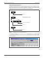
MELSEC-L Series
Programmable Logic Controllers
User's Manual
IO-Link Master Module
ME1IOL6-L
Art. no.: 254015
23 07 2012
Version A
MITSUBISHI ELECTRIC
INDUSTRIAL AUTOMATION
Version check
About this Manual
The texts, illustration, diagrams and examples in this manual are provided for information
purposes only. They are intended as aids to help explain the installation, operation,
programming and use of the programmable logic controllers of
the MELSEC-L series.
If you have any questions about the installation and operation of any of the products described in this
manual please contact your local sales office or distributor (see back cover).
You can find the latest information and answers to frequently asked questions
on our website at www.mitsubishi-automation.com.
MITSUBISHI ELECTRIC EUROPE BV reserves the right to make changes to this manual or the technical
specifications of its products at any time without notice.
© 2012
A
Version
07/2012
pdp-dk
IO-Link Master Module
ME1IOL6-L
User's Manual
Art.-no.: 254015
Changes / Additions / Corrections
First edition
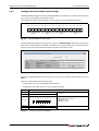
Safety Guidelines
For use by qualified staff only
This manual is only intended for use by properly trained and qualified electrical technicians who are
fully acquainted with the relevant automation technology safety standards. All work with the hardware described, including system design, installation, configuration, maintenance, service and testing of the equipment, may only be performed by trained electrical technicians with approved qualifications who are fully acquainted with all the applicable automation technology safety standards
and regulations. Any operations or modifications to the hardware and/or software of our products not
specifically described in this manual may only be performed by authorised Mitsubishi Electric staff.
Proper use of the products
The programmable logic controllers of the MELSEC-L series are only intended for the specific applications explicitly described in this manual. All parameters and settings specified in this manual must
be observed. The products described have all been designed, manufactured, tested and documented
in strict compliance with the relevant safety standards. Unqualified modification of the hardware or
software or failure to observe the warnings on the products and in this manual may result in serious
personal injury and/or damage to property. Only peripherals and expansion equipment specifically
recommended and approved by Mitsubishi Electric may be used with the programmable logic controllers of the MELSEC-L series.
All and any other uses or application of the products shall be deemed to be improper.
Relevant safety regulations
All safety and accident prevention regulations relevant to your specific application must be observed
in the system design, installation, configuration, maintenance, servicing and testing of these products. The installation should be carried out in accordance to applicable local and national standards.
Safety warnings in this manual
In this manual warnings that are relevant for safety are identified as follows:
m
DANGER:
b
WARNING:
Failure to observe the safety warnings identified with this symbol can result in health and injury
hazards for the user.
Failure to observe the safety warnings identified with this symbol can result in damage to the
equipment or other property.
MELSEC-L series — IO-Link Master Module ME1IOL6-L
I
General safety information and precautions
The following safety precautions are intended as a general guideline for using PLC systems together
with other equipment. These precautions must always be observed in the design, installation and
operation of all control systems.
m
DANGER:
● Observe all safety and accident prevention regulations applicable to your specific application. Always disconnect all power supplies before performing installation and wiring work
or opening any of the assemblies, components and devices.
● Assemblies, components and devices must always be installed in a shockproof housing fitted
with a proper cover and fuses or circuit breakers.
● Devices with a permanent connection to the mains power supply must be integrated in the
building installations with an all-pole disconnection switch and a suitable fuse.
● Check power cables and lines connected to the equipment regularly for breaks and insulation
damage. If cable damage is found immediately disconnect the equipment and the cables
from the power supply and replace the defective cabling.
● Before using the equipment for the first time check that the power supply rating matches that
of the local mains power.
● Take appropriate steps to ensure that cable damage or core breaks in the signal lines cannot
cause undefined states in the equipment.
● You are responsible for taking the necessary precautions to ensure that programs interrupted by brownouts and power failures can be restarted properly and safely. In particular, you
must ensure that dangerous conditions cannot occur under any circumstances, even for brief
periods.
● EMERGENCY OFF facilities conforming to EN 60204/IEC 204 and VDE 0113 must remain fully
operative at all times and in all PLC operating modes. The EMERGENCY OFF facility reset
function must be designed so that it cannot ever cause an uncontrolled or undefined restart.
● You must implement both hardware and software safety precautions to prevent the possibility of undefined control system states caused by signal line cable or core breaks.
● When using modules always ensure that all electrical and mechanical specifications and
requirements are observed exactly.
II
Contents
Contents
1
Overview
1.1
IO-Link System Overview . . . . . . . . . . . . . . . . . . . . . . . . . . . . . . . . . . . . . . . . . . . . . . . . . . . . . . . . . 1-1
1.1.1
Data exchange in an IO-Link System. . . . . . . . . . . . . . . . . . . . . . . . . . . . . . . . . . . . . . 1-1
1.2
Features of the ME1IOL6-L . . . . . . . . . . . . . . . . . . . . . . . . . . . . . . . . . . . . . . . . . . . . . . . . . . . . . . . . 1-2
2
System Configuration
2.1
Overall System Configuration . . . . . . . . . . . . . . . . . . . . . . . . . . . . . . . . . . . . . . . . . . . . . . . . . . . . . 2-1
2.2
Applicable System. . . . . . . . . . . . . . . . . . . . . . . . . . . . . . . . . . . . . . . . . . . . . . . . . . . . . . . . . . . . . . . . 2-1
3
Quick start IO-Link
3.1
Enabling IO-Link communication . . . . . . . . . . . . . . . . . . . . . . . . . . . . . . . . . . . . . . . . . . . . . . . . . 3-2
3.2
Verifying IO-Link communication . . . . . . . . . . . . . . . . . . . . . . . . . . . . . . . . . . . . . . . . . . . . . . . . . 3-3
3.3
Input process data. . . . . . . . . . . . . . . . . . . . . . . . . . . . . . . . . . . . . . . . . . . . . . . . . . . . . . . . . . . . . . . . 3-4
3.4
Output process data . . . . . . . . . . . . . . . . . . . . . . . . . . . . . . . . . . . . . . . . . . . . . . . . . . . . . . . . . . . . . . 3-5
4
Detailed Description of the Module
4.1
Part Names. . . . . . . . . . . . . . . . . . . . . . . . . . . . . . . . . . . . . . . . . . . . . . . . . . . . . . . . . . . . . . . . . . . . . . . 4-1
4.1.1
4.2
Specifications . . . . . . . . . . . . . . . . . . . . . . . . . . . . . . . . . . . . . . . . . . . . . . . . . . . . . . . . . . . . . . . . . . . . 4-3
4.2.1
4.3
Signal Layout of the Terminal Block . . . . . . . . . . . . . . . . . . . . . . . . . . . . . . . . . . . . . . 4-2
External Dimensions . . . . . . . . . . . . . . . . . . . . . . . . . . . . . . . . . . . . . . . . . . . . . . . . . . . . 4-4
Functions of the IO-Link Master Module . . . . . . . . . . . . . . . . . . . . . . . . . . . . . . . . . . . . . . . . . . . 4-5
4.3.1
IO-Link Master Function . . . . . . . . . . . . . . . . . . . . . . . . . . . . . . . . . . . . . . . . . . . . . . . . . 4-5
4.3.2
Input and Output Data in IO-Link Mode or SIO Mode. . . . . . . . . . . . . . . . . . . . . . 4-5
4.3.3
Masking of Input Data . . . . . . . . . . . . . . . . . . . . . . . . . . . . . . . . . . . . . . . . . . . . . . . . . . . 4-7
4.3.4
Output HOLD/CLEAR Function . . . . . . . . . . . . . . . . . . . . . . . . . . . . . . . . . . . . . . . . . . . 4-8
4.3.5
Data Swapping Function. . . . . . . . . . . . . . . . . . . . . . . . . . . . . . . . . . . . . . . . . . . . . . . . . 4-9
4.3.6
Exchange of Consistent Data . . . . . . . . . . . . . . . . . . . . . . . . . . . . . . . . . . . . . . . . . . . . 4-10
4.3.7
Reading and Writing of Parameter Data . . . . . . . . . . . . . . . . . . . . . . . . . . . . . . . . . 4-11
4.3.8
Direct Parameter Page . . . . . . . . . . . . . . . . . . . . . . . . . . . . . . . . . . . . . . . . . . . . . . . . . . 4-13
4.3.9
Automatic Confirmation of Events . . . . . . . . . . . . . . . . . . . . . . . . . . . . . . . . . . . . . . 4-14
MELSEC-L series — IO-Link Master Module ME1IOL6-L
V
Contents
4.4
4.5
4.3.10
Data Storage . . . . . . . . . . . . . . . . . . . . . . . . . . . . . . . . . . . . . . . . . . . . . . . . . . . . . . . . . . . 4-14
4.3.11
Device Validation . . . . . . . . . . . . . . . . . . . . . . . . . . . . . . . . . . . . . . . . . . . . . . . . . . . . . . . 4-16
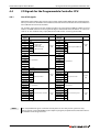
I/O Signals for the Programmable Controller CPU. . . . . . . . . . . . . . . . . . . . . . . . . . . . . . . . . 4-18
4.4.1
List of I/O signals . . . . . . . . . . . . . . . . . . . . . . . . . . . . . . . . . . . . . . . . . . . . . . . . . . . . . . . 4-18
4.4.2
Details of Input Signals . . . . . . . . . . . . . . . . . . . . . . . . . . . . . . . . . . . . . . . . . . . . . . . . . 4-19
4.4.3
Details of Output Signals. . . . . . . . . . . . . . . . . . . . . . . . . . . . . . . . . . . . . . . . . . . . . . . . 4-20
Buffer Memory . . . . . . . . . . . . . . . . . . . . . . . . . . . . . . . . . . . . . . . . . . . . . . . . . . . . . . . . . . . . . . . . . . 4-21
4.5.1
Buffer memory assignment . . . . . . . . . . . . . . . . . . . . . . . . . . . . . . . . . . . . . . . . . . . . . 4-22
4.5.2
CH Input Process Data (Un\G0 to Un\G15, Un\G16 to Un\G31...) . . . . . . . . 4-31
4.5.3
CH Output Process Data (Un\G112 to Un\G127, Un\G128 to Un\G143...) 4-31
4.5.4
CH Input Data Mask (Un\G224, Un\G225 to Un\G229). . . . . . . . . . . . . . . . . . 4-31
4.5.5
Output Data Consistency Enable (Un\G230) . . . . . . . . . . . . . . . . . . . . . . . . . . . . . 4-32
4.5.6
Changing the Channel Mode (Un\G240 to Un\G253) . . . . . . . . . . . . . . . . . . . . . 4-32
4.5.7
CH Current Mode (Un\G272, Un\G273...) . . . . . . . . . . . . . . . . . . . . . . . . . . . . . . . 4-35
4.5.8
Data Storage Setting (Un\G255) . . . . . . . . . . . . . . . . . . . . . . . . . . . . . . . . . . . . . . . . . 4-35
4.5.9
Current Data Storage Setting (Un\G279) . . . . . . . . . . . . . . . . . . . . . . . . . . . . . . . . . 4-36
4.5.10
Channel Error Flag (Un\G280), Channel Error Reset Flag (Un\G281) . . . . . . . 4-37
4.5.11
Module diagnostic information (Un\G282). . . . . . . . . . . . . . . . . . . . . . . . . . . . . . . 4-38
4.5.12
CH Diagnostic information (Un\G283, Un\G284...). . . . . . . . . . . . . . . . . . . . . . 4-39
4.5.13
IO-Link event information (Un\G320 to Un\G370) . . . . . . . . . . . . . . . . . . . . . . . . 4-40
4.5.14
CH Acyclic Communication Request (Un\G416 to Un\G1267) . . . . . . . . . . 4-44
4.5.15
Acyclic Communication Request Flags (Un\G1280) . . . . . . . . . . . . . . . . . . . . . . 4-47
4.5.16
Acyclic Communication Response Flags (Un\G1281) . . . . . . . . . . . . . . . . . . . . . 4-47
4.5.17
CH Acyclic Communication Answer (Un\G1296 to Un\G2148). . . . . . . . . . 4-48
4.5.18
Direct Parameter Page 1 (DPP1) Read Access . . . . . . . . . . . . . . . . . . . . . . . . . . . . 4-51
5
Setup and Procedures before Operation
5.1
Handling Precautions. . . . . . . . . . . . . . . . . . . . . . . . . . . . . . . . . . . . . . . . . . . . . . . . . . . . . . . . . . . . . 5-1
5.2
Getting started . . . . . . . . . . . . . . . . . . . . . . . . . . . . . . . . . . . . . . . . . . . . . . . . . . . . . . . . . . . . . . . . . . 5-1
5.3
Installation Environment and Installation Position . . . . . . . . . . . . . . . . . . . . . . . . . . . . . . . . . 5-2
5.3.1
5.4
VI
Safety Precautions . . . . . . . . . . . . . . . . . . . . . . . . . . . . . . . . . . . . . . . . . . . . . . . . . . . . . . . 5-2
Wiring . . . . . . . . . . . . . . . . . . . . . . . . . . . . . . . . . . . . . . . . . . . . . . . . . . . . . . . . . . . . . . . . . . . . . . . . . . . 5-4
5.4.1
Wiring precautions . . . . . . . . . . . . . . . . . . . . . . . . . . . . . . . . . . . . . . . . . . . . . . . . . . . . . . 5-4
5.4.2
External wiring . . . . . . . . . . . . . . . . . . . . . . . . . . . . . . . . . . . . . . . . . . . . . . . . . . . . . . . . . . 5-5
Contents
5.5
PLC Parameter Setting . . . . . . . . . . . . . . . . . . . . . . . . . . . . . . . . . . . . . . . . . . . . . . . . . . . . . . . . . . . . 5-7
5.5.1
I/O assignment . . . . . . . . . . . . . . . . . . . . . . . . . . . . . . . . . . . . . . . . . . . . . . . . . . . . . . . . . . 5-7
5.5.2
Intelligent function module switch settings. . . . . . . . . . . . . . . . . . . . . . . . . . . . . . . 5-8
5.6
Setting of the IO-Link Devices. . . . . . . . . . . . . . . . . . . . . . . . . . . . . . . . . . . . . . . . . . . . . . . . . . . . . 5-9
6
Programming
6.1
Programming Procedure . . . . . . . . . . . . . . . . . . . . . . . . . . . . . . . . . . . . . . . . . . . . . . . . . . . . . . . . . 6-1
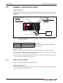
6.2
Example 1: Input of Process Data. . . . . . . . . . . . . . . . . . . . . . . . . . . . . . . . . . . . . . . . . . . . . . . . . . 6-2
6.3
6.4
6.5
6.2.1
Before creating a program . . . . . . . . . . . . . . . . . . . . . . . . . . . . . . . . . . . . . . . . . . . . . . . 6-2
6.2.2
Program. . . . . . . . . . . . . . . . . . . . . . . . . . . . . . . . . . . . . . . . . . . . . . . . . . . . . . . . . . . . . . . . . 6-4
Example 2: Output of Process Data . . . . . . . . . . . . . . . . . . . . . . . . . . . . . . . . . . . . . . . . . . . . . . . . 6-7
6.3.1
Before creating a program . . . . . . . . . . . . . . . . . . . . . . . . . . . . . . . . . . . . . . . . . . . . . . . 6-7
6.3.2
Program. . . . . . . . . . . . . . . . . . . . . . . . . . . . . . . . . . . . . . . . . . . . . . . . . . . . . . . . . . . . . . . . . 6-7
Example 3: Acyclic Communication (Reading) . . . . . . . . . . . . . . . . . . . . . . . . . . . . . . . . . . . . . 6-9
6.4.1
Before creating a program . . . . . . . . . . . . . . . . . . . . . . . . . . . . . . . . . . . . . . . . . . . . . . . 6-9
6.4.2
Program. . . . . . . . . . . . . . . . . . . . . . . . . . . . . . . . . . . . . . . . . . . . . . . . . . . . . . . . . . . . . . . . . 6-9
Example 4: Acyclic Communication (Writing) . . . . . . . . . . . . . . . . . . . . . . . . . . . . . . . . . . . . . 6-11
6.5.1
Before creating a program . . . . . . . . . . . . . . . . . . . . . . . . . . . . . . . . . . . . . . . . . . . . . . 6-11
6.5.2
Program. . . . . . . . . . . . . . . . . . . . . . . . . . . . . . . . . . . . . . . . . . . . . . . . . . . . . . . . . . . . . . . . 6-11
7
Troubleshooting
7.1
Troubleshooting using the LEDs of the Module . . . . . . . . . . . . . . . . . . . . . . . . . . . . . . . . . . . . 7-1
7.1.1
When the "RUN" LED is turned off . . . . . . . . . . . . . . . . . . . . . . . . . . . . . . . . . . . . . . . . 7-1
7.1.2
When any of the LEDs "1" to "6" is off . . . . . . . . . . . . . . . . . . . . . . . . . . . . . . . . . . . . . 7-1
7.1.3
When any of the LEDs "1" to "6" lights red . . . . . . . . . . . . . . . . . . . . . . . . . . . . . . . . 7-2
7.2
Errors related to Process Data . . . . . . . . . . . . . . . . . . . . . . . . . . . . . . . . . . . . . . . . . . . . . . . . . . . . . 7-3
7.3
Errors related to Acyclic Communication . . . . . . . . . . . . . . . . . . . . . . . . . . . . . . . . . . . . . . . . . . 7-4
7.4
Checking the IO-Link Master Module Status . . . . . . . . . . . . . . . . . . . . . . . . . . . . . . . . . . . . . . . 7-5
MELSEC-L series — IO-Link Master Module ME1IOL6-L
VII
Contents
VIII
IO-Link System Overview
1
Overview
Overview
This User's Manual describes the specifications, handling and programming methods for the IO-Link
Master Module ME1IOL6-L (hereinafter referred to as the ME1IOL6-L) which is used with the programmable controllers of the MELSEC-L series.
Before using the ME1IOL6-L, please read this manual and the relevant manuals carefully and develop
familiarity with the functions and performance of the MELSEC-L series programmable controller to
handle the product correctly.
1.1
IO-Link System Overview
The ME1IOL6-L is a master module for IO-Link. Up to six IO-Link devices (slaves) or conventional I/O
devices can be connected to a single ME1IOL6-L.
An IO-Link system consists of IO-Link devices (often sensors, actuators or combinations thereof ), a
standard 3-wire sensor/actuator cable and an IO-Link master.
Only one IO-Link device can be connected to each port of the master. Thus IO-Link is point-to-point
communication and not a fieldbus.
1.1.1
Data exchange in an IO-Link System
Two types of data may basically be exchanged:
● Cyclic data (process data)
● Acyclic data (service data)
Cyclic data is exchanged automatically. Acyclic data is exchanged only after a request of the IO-Link
master.
Process data
Process data can be comprised of process input data and/or process output data. The process data of
the devices is transmitted cyclically in a data frame. In some cases the process data is split up and
transmitted in several cycles.
A diagnostic flag indicates that the process data is invalid.
Service data
Service data can be comprised of on-request data objects and events. Service data is always
exchanged acyclically and always upon request of the IO-Link master. First, the IO-Link master sends
a request to the device and the device responds. This is true for writing data to the device as well as
for reading data from the device. Service data can be used to read out parameter values or device
states. It can also be used to write parameter values or to send commands.
When an event occurs the device notifies the master. The master responds and reads out the reported
event. This means that events or device states such as low supply voltage, short circuit, etc. can be
transmitted via the IO-Link master to the PLC.
More information
This short overview about IO-Link is only a extract of the information provided on the website of the
IO-Link Consortium. You can find much more information about IO-Link and answers to frequently
asked questions on their website at www.io-link-com.
MELSEC-L series — IO-Link Master Module ME1IOL6-L
1–1
Overview
1.2
Features of the ME1IOL6-L
Features of the ME1IOL6-L
IO-Link master function
Up to six IO-Link devices can be connected to a single ME1IOL6-L.
Various modes selectable
Each channel of the ME1IOL6-L can be configured to run in IO-Link mode, in digital input mode (SIO
mode), digital output mode (SIO mode) or can be deactivated.
Useful functions for data input and output
The following functions are available in IO-Link mode:
● Automatic update of input and output process data
● Exchange of consistent data
● Masking of input data
● Data valid output HOLD/CLEAR
● Data swapping
In SIO mode, the HOLD/CLEAR function is available in output mode.
Acyclic communication
In addition to the cyclic communication between the IO-Link master and an IO-Link device, data can
be exchanged using acyclic communication.
Convenient functions associated with IO-Link devices
● Direct parameter page access
● Automatic confirmation of events
● Data storage for automatic IO-Link devices parameter back-up
● Device validation
For a detailed description of the functions of the ME1IOL6-L, please refer to section 4.3.
1–2
Overall System Configuration
System Configuration
2
System Configuration
2.1
Overall System Configuration
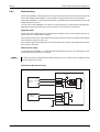
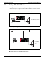
The following shows a system configuration example for using the IO-Link master module.
Display unit (optional)
Power supply module
Fig. 2-1:
CPU module
IO-Link master module
ME1IOL6-L
I/O module or
intelligent function
module
End cover
Connection of the ME1IOL6-L to a CPU module
For the installation of the PLC and the mounting of modules, please refer to the User's Manual for the
CPU modules of the MELSEC-L series (Hardware design, Maintenance and Inspection).
2.2
Applicable System
Number of connectable modules
The number of I/O modules and intelligent function modules that can be connected in a system is 10
in total*. If more than 10 modules are connected, the CPU module detects "SP.UNIT LAY ERR." (error
code: 2124).
* The number of modules is exclusive of the number of power supply modules, CPU modules, display units, RS-232 adapters, and END covers.
There is no restriction on the number of IO-Link master modules ME1IOL6-L as long as the total number of modules is 10 or less.
Compatible software version
For the programming and monitoring of ME1IOL6-L installed in a MELSEC-L series PLC use GX Works2.
GX Developer can also be used.
MELSEC-L series — IO-Link Master Module ME1IOL6-L
2–1
System Configuration
2–2
Applicable System
Quick start IO-Link
3
Quick start IO-Link
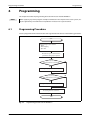
This chapter explains based on a simple programming example how to start IO-Link communication
with the IO-Link Master.
A comprehensive description can be found in chapter 5 of this manual.
Start
Fig. 3-1:
Module mounting
Mount the ME1IOL6-L to the L series PLC.
Refer to section 5.3
Wiring
Connect the external power supply and
the IO-Link devices.
Refer to section 5.4
Programming and debugging
Create and check the sequence program.
Refer to chapter 6
Function chart for the setup of an IO-Link master module ME1IOL6-L
MELSEC-L series — IO-Link Master Module ME1IOL6-L
3–1
Quick start IO-Link
3.1
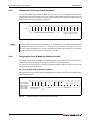
Enabling IO-Link communication
Enabling IO-Link communication
After setting the IO-Link master to IO-Link mode, IO-Link communication with the connected IO-Link
Devices is started. Please note that in the following example the ME1IOL6-L occupies the input and
output addresses X/Y40 to X/Y5F.
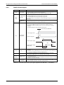
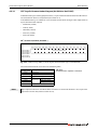
�
�
�
�
�
�
쐆
Fig. 3-2:
Number
Settings for channels CH1 to CH6
Description
�
Channel CH1
�
Channel CH2
�
�
The relevant channel set to: IO-Link mode, data swapping, fastest possible cycle time
�
Tab. 3-1:
3–2
Channel CH4
Channel CH5
�
쐆
Channel CH3
Channel CH6
The channel mode change flags for CH1 to CH6 are set.
Description of the program for the settings
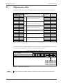
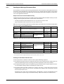
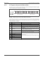
Verifying IO-Link communication
3.2
Quick start IO-Link
Verifying IO-Link communication
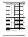
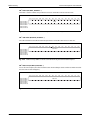
The current mode of each channel can be checked in the current mode registers:
Address
Value
Description
Hexadecimal
Decimal
110H
272
CH1
0
0
0
0
0
0
0
1
0
0
0
1
0
1
1
1
111H
273
CH2
0
0
0
0
0
0
0
1
0
0
0
1
0
1
1
1
112H
274
CH3
0
0
0
0
0
0
0
1
0
0
0
1
0
1
1
1
113H
275
CH4
0
0
0
0
0
0
0
1
0
0
0
1
0
1
1
1
114H
276
CH5
0
0
0
0
0
0
0
1
0
0
0
1
0
1
1
1
115H
277
CH6
0
0
0
0
0
0
0
1
0
0
1
0
1
0
0
1
High Byte
Current mode
Low Byte
Bit 8: 1 = IO-Link mode
Tab. 4-2:
Value of the current mode registers
Please note, that the low byte values in the above table are depending on the cycle time settings of
your current configuration and can differ from the shown status of the bits.
Active IO-Link communication with a connected device is shown in the channel diagnostic registers:
Address
Value
Description
Hexadecimal
Decimal
11BH
283
CH1
0
0
0
0
0
0
0
0
1
0
0
0
0
0
0
0
11CH
284
CH2
0
0
0
0
0
0
0
0
1
0
0
0
0
0
0
0
11DH
285
CH3
0
0
0
0
0
0
0
0
1
0
0
0
0
0
0
0
11EH
286
CH4
0
0
0
0
0
0
0
0
1
0
0
0
0
0
0
0
11FH
287
CH5
0
0
0
0
0
0
0
0
1
0
0
0
0
0
0
0
120H
288
CH6
0
0
0
0
0
0
0
0
1
0
0
0
0
0
0
0
High Byte
Diagnostic
information
Low Byte
Bit 7: 1 = Device connected
Tab. 4-3:
NOTE
Value of the channel diagnostic registers
Refer to section 4.5.1 for buffer memory assignment.
MELSEC-L series — IO-Link Master Module ME1IOL6-L
3–3
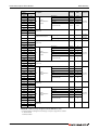
Input process data
3.3
Quick start IO-Link
Input process data
The input process data is received from the IO-Link Device and written to the buffer memory automatically.
Address
Hexadecimal
Decimal
High byte
Description
Low byte
0H
0
Byte 1
Byte 0
1H
1
Byte 3
Byte 2
to
to
…
…
FH
15
Byte 31
Byte 30
10H
16
Byte 1
Byte 0
CH1
Input process data in IO-Link mode
to
to
…
…
1FH
31
Byte 31
Byte 30
20H
32
Byte 1
Byte 0
CH2
Input process data in IO-Link mode
to
to
…
…
2FH
47
Byte 31
Byte 30
30H
48
Byte 1
Byte 0
CH3
Input process data in IO-Link mode
to
to
…
…
3FH
63
Byte 31
Byte 30
40H
64
Byte 1
Byte 0
to
5FH
95
Tab. 3-4:
CH6
Input process data in IO-Link mode
Byte 31
Byte 30
Byte 1
Byte 0
…
80
to
Input process data in IO-Link mode
…
50H
CH5
…
to
79
Input process data in IO-Link mode
…
to
4FH
CH4
Byte 31
Byte 30
Input process data allocation in buffer memory (data swap enabled)
If the input data invalid flags in IO-Link mode are showing a high signal either there is no IO-Link communication or the input process data is marked as invalid by the IO-Link Device.
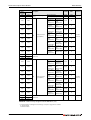
Signal direction CPU Module ME1IOL6-L
Device No. (Input)
Value
F
E
D
C
B
A
9
8
7
6
5
4
3
2
1
X40–X4F
0
0
0
0
0
0
0
0
1
0
0
0
0
0
0
0
1
X50–X5F
0
0
0
0
0
0
0
0
0
0
0
0
0
0
0
0
X51: CH1 input data is valid
X52: CH2 input data is valid
X53: CH3 input data is valid
X54: CH4 input data is valid
X55: CH5 input data is valid
X56: CH6 input data is valid
Tab. 4-5:
Value of the input devices
MELSEC-L series — IO-Link Master Module ME1IOL6-L
3–4
Output process data
3.4
Quick start IO-Link
Output process data
The output process data stored in the buffer memory is sent to the IO-Link Device automatically.
Address
8FH
143
90H
144
to
to
9FH
159
A0H
160
to
to
AFH
175
B0H
176
to
to
BFH
191
C0H
192
to
to
CFH
207
Tab. 3-6:
CH2
CH3
CH4
CH5
CH6
Output process data in IO-Link mode
Output process data in IO-Link mode
Output process data in IO-Link mode
Output process data in IO-Link mode
Output process data in IO-Link mode
Byte 1
Byte 0
Byte 31
Byte 30
Byte 1
Byte 0
Byte 31
Byte 30
Byte 1
Byte 0
Byte 31
Byte 30
Byte 1
Byte 0
Byte 31
Byte 30
Byte 1
Byte 0
…
to
Byte 30
…
128
to
Byte 31
…
80H
Byte 2
…
127
Byte 3
Output process data in IO-Link mode
…
7FH
CH1
…
to
Byte 0
…
113
to
Byte 1
…
71H
Low byte
…
112
High byte
…
70H
Description
…
Decimal
…
Hexadecimal
Byte 31
Byte 30
Output process data allocation in buffer memory (data swap enabled)
In case of IO-Link process output data the IO-Link master needs to send an output data valid to the IOLink device. For this purpose it is necessary to set the appropriate signals:
Signal direction CPU Module ME1IOL6-L
Device No. (Output)
Value
F
E
D
C
B
A
9
8
7
6
5
4
3
2
1
0
Y40–Y4F
0
0
0
0
0
0
0
0
0
0
0
0
0
0
0
0
Y50–Y5F
0
0
0
0
0
0
0
0
0
1
1
1
1
1
1
0
Y51: CH1 output data is valid
Y52: CH2 output data is valid
Y53: CH3 output data is valid
Y54: CH4 output data is valid
Y55: CH5 output data is valid
Y56: CH6 output data is valid
Tab. 4-7:
NOTE
Value of the output devices
Refer to section 4.5.1 for buffer memory assignment and section 4.4.1 for the list of I/O signals.
MELSEC-L series — IO-Link Master Module ME1IOL6-L
3–5
Output process data
MELSEC-L series — IO-Link Master Module ME1IOL6-L
Quick start IO-Link
3–6
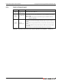
Part Names
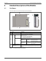
Detailed Description of the Module
4
Detailed Description of the Module
4.1
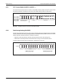
Part Names
This section explains the names of the components for the ME1IOL6-L
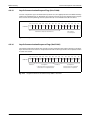
�
�
�
�
�
Fig. 4-1:
Names of parts
No.
Name
�
Module joint levers
Description
Levers for connecting two modules
�
DIN rail hook
A hook used to mount the module to a DIN rail.
RUN
Displays the operating status of the ME1IOL6-L.
On: Normal operation
Off: – Internal power supply (5 V DC) is OFF.
– External power supply (24 V DC) is OFF.
– An internal error has occurred.
Indicates the I/O status of each channel of the ME1IOL6-L.
�
LEDs
SIO mode
On (red):
On (green):
Off:
IO-Link mode
On (red):
An error has occurred on this channel.
Flashing (green): Channel does IO-Link communication
Off:
– Not connected
1 to 6
�
An error has occurred on this channel.
Input/output signal is ON
Input/output signal is OFF
Detachable terminal block
Used for connection of the sensors or actuator and the external power supply.
Terminal cover
A cover for preventing touching the terminals.
A label on it is used for recording the signal names of devices allocated to
terminals.
Tab. 4-1:
Description of the parts of the ME1IOL6-L
MELSEC-L series — IO-Link Master Module ME1IOL6-L
4–1
Detailed Description of the Module
4.1.1
Part Names
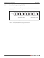
Signal Layout of the Terminal Block
Terminal No.
Signal name
1
2
L+1
CH1
C1
3
4
L+2
CH2
C2
5
6
L+3
CH3
C3
7
8
L+4
CH4
C4
9
10
L+5
CH5
C5
11
12
L+6
CH6
C6
Description
+24 V DC
Power supply output for connected sensor/actuator
SIO mode
Switching signal DI/DO
IO-Link mode
"Coded switching" (Communication line)
+24 V DC
Power supply output for connected sensor/actuator
SIO mode
Switching signal DI/DO
IO-Link mode
"Coded switching" (Communication line)
+24 V DC
Power supply output for connected sensor/actuator
SIO mode
Switching signal DI/DO
IO-Link mode
"Coded switching" (Communication line)
+24 V DC
Power supply output for connected sensor/actuator
SIO mode
Switching signal DI/DO
IO-Link mode
"Coded switching" (Communication line)
+24 V DC
Power supply output for connected sensor/actuator
SIO mode
Switching signal DI/DO
IO-Link mode
"Coded switching" (Communication line)
+24 V DC
Power supply output for connected sensor/actuator
SIO mode
Switching signal DI/DO
IO-Link mode
"Coded switching" (Communication line)
0V
Power supply output for connected sensors/actuators
13
L-
14
L-
15
L-
16
+ 24V
17
24G
0V
18
(FG)
Frame Ground
Tab. 4-2:
+24 V DC
External power supply input
Signal layout for the detachable terminal block of the ME1IOL6-L
For the wiring of the IO-Link master module ME1IOL6-L please refer to section 5.4.
4–2
Specifications
4.2
Detailed Description of the Module
Specifications
The specifications for the ME1IOL6-L are shown in the following table. For general specifications,
please refer to the User's Manual for the CPU modules of the MELSEC-L series (Hardware design, Maintenance and Inspection).
Item
Specifications
Number of ports
6
앫IO-Link
앫Digital output (SIO mode)
앫Digital input (SIO mode)
앫Disabled
Port configuration
IO-Link mode
Rated voltage
24 V DC
Rated output current (C/Q)
15 mA
Rated sensor/actuator supply
current (L+)
200 mA
Input type
Sink
Rated voltage
Digital input
SIO mode
Digital output
24 V DC
Internal pull-down current
(C/Q)
5 mA
Input filter (HW and SW)
200 μs
Rated voltage
24 V DC
Rated output current (C/Q)
200 mA
Rated sensor/actuator supply
current (L+)
200 mA
Output type
Max. current per port (sum of
C and L+): 215 mA
Push-pull
Communication line (C/Q)
Port disabled
Protection
functions
Insulation
method
Sensor/actuator supply line
(L+)
Communication line (C/Q)
Sensor/actuator supply line (L+)
Between the I/O terminals and PLC power
supply
Between channels
Switched OFF
Over-current, over-load and short-circuit
Photocoupler isolation
No isolation
Dielectric withstand voltage
Between I/O terminals and programmable controller power
supply: 500 V ACrms for 1 minute
Insulation resistance
Between I/O terminals and programmable controller power
supply: 500 V DC, 10 M: or more
Number of occupied I/O points
External wiring connection system
Cable type
Maximum length
Cable specification
Applicable wire size
18-points terminal block
Unshielded cable
20 m
0.3 to 0.75mm2
Overall loop resistance
6:
Effective line capacitance
3 nF
Applicable solderless terminals
R1.25-3 (Solderless terminals with sleeves cannot be used.)
Voltage
24 V DC (+20%, -15%); ripple, spike within 500mVP-P
In order to keep the specified IO-Link output voltage
levels (L+ line) the external supply voltage must be higher
than 22 V DC.
Current
The sum current on the L- lines must not exceed 1.7 A.
External supply power
Inrush current
Internal current consumption (5 V DC)
Online module change
Weight
Tab. 4-3:
32 points (I/O assignment: Intelligent 32 points)
8 A within 230 μs
0.4 A
Not supported
180 g
Specifications of the ME1IOL6-L
MELSEC-L series — IO-Link Master Module ME1IOL6-L
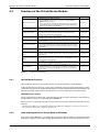
4–3
Detailed Description of the Module
External Dimensions
90
45
4
4.2.1
Specifications
(45)
DIN rail center
4
4
95
117
28.5
(Unit: mm)
Fig. 4-2:
4–4
Dimensions of the ME1IOL6-L
Functions of the IO-Link Master Module
4.3
Functions of the IO-Link Master Module
Function
Description
IO-Link master function
Communication with IO-Link devices
Up to six IO-Link devices can be connected to a single ME1IOL6-L.
FDT/DTM function support
Using a commercially available FDT (Field Device Tool), reading/writing the IO-Link device’s parameters and monitoring the IO-Link device
status are executable via the ME1IOL6-L.
Section 4.3.1
Various modes selectable
Each channel of the ME1IOL6-L can configured to run in IO-Link mode, in
Standard I/0 mode (SIO mode) or can be deactivated.
Section 4.3.2
Masking of input data
To recognize certain bits in the first two bytes of the input data, an input
data mask can be used to filter the input process data. The result is
shown for each channel on an input signal.
Section 4.3.3
Output HOLD/CLEAR
The output status can be retained when the PLC CPU module is placed in
the STOP status or when an error occurs.
Section 4.3.4
Data swapping
For communication with an IO-device, the order of bytes can be changed
for each channel.
Section 4.3.5
Exchange of consistent
data
The exchange of more than two bytes of process data in a consistent way
or the synchronization between reading input data and writing output
data is possible by using the consistency handshake signals provided by
the ME1IOL6-L.
Section 4.3.6
Acyclic communication
In addition to the cyclic communication between the IO-Link master and
an IO-Link device, data can be exchanged using acyclic communication.
Section 4.3.7
Direct parameter page
access
The direct parameter page 1 of an IO-Link device can be accessed by
using the acyclic communication interface or the direct mapping in the
buffer memory.
Section 4.3.8
Automatic confirmation of
events
By sending event data to the IO-Link master, an IO-Link device can
inform about warnings, errors or certain states. The ME1IOL6-L can confirm these events automatically.
Section 4.3.9
Data storage
The ME1IOL6-L can backup parameter data from the IO-Link device and
also can write these data back to the device.
Section 4.3.10
Device validation
When the device validation is activated the ME1IOL6-L checks the connected IO-Link device at every start-up of the IO-Link communication. A
device error is indicated by the ME1IOL6-L in case that the validation is
not successful.
Section 4.3.11
Tab. 4-4:
4.3.1
Detailed Description of the Module
Reference
Functions of the ME1IOL6-L
IO-Link Master Function
Up to six IO-Link devices or conventional devices can be connected to a single ME1IOL6-L.
In IO-Link mode process data (e.g. analog values, switching states) are exchanged cyclically, configuration data (e.g. activation, deactivation of functions) as well as identification data (manufacturer ID)
typically at startup, and parameters or diagnostics are sent as needed (acyclic communication).
FDT/DTM function support
Using a commercially available FDT, reading/writing the IO-Link device parameters and monitoring
the IO-Link device status are executable via the ME1IOL6-L.
Refer to section 5.6 (Setting of the IO-Link devices) for more details about the FDT/DTM* system
structure.
* FDT stands for Field Device Tool and DTM stands for Device Type Manager. FDT/DTM is a communication technique for
the manufacturer-independent configuration of field devices.
4.3.2
Input and Output Data in IO-Link Mode or SIO Mode
Each channel of the ME1IOL6-L can configured to run either in IO-Link mode or in Standard I/0 mode
(SIO mode) as digital input or digital output. Mixed operation of IO-Link and conventional devices is
MELSEC-L series — IO-Link Master Module ME1IOL6-L
4–5
Detailed Description of the Module
Functions of the IO-Link Master Module
possible. A channel can also be deactivated. In this case, the 24 V DC voltage output on the channels
L+ line is switched OFF.
To change the mode of a channel of the IO-Link master module, the user has to set the corresponding
mode change bit of the channel in the buffer memory address Un\G240. The module will try to
change the mode and stores the result of the operation in an other buffer memory address. For more
information about the mode changing please refer to section 4.5.6.
IO-Link mode
● Input data
In IO-Link mode, the input process data (up to 32 bytes per channel) from the connected IO-Link
device is stored in the buffer memory of the ME1IOL6-L. The size and the structure of the data
depends on the connected device. Therefore, the ME1IOL6-L maps the data straight into the input
process data area without any interpretation (refer to section 4.5.2).
In case that IO-Link communication stops (e.g. due to undervoltage, disconnection of an IO-Link
Device) the input process data buffer is set to 0.
● Output data
In IO-Link mode, output process data (up to 32 bytes per channel) stored in the buffer memory is
output to the connected IO-Link device. The size and the structure of the data depends on the
connected device.
To send output data to the IO-Link device it is necessary to set the corresponding data valid signal
Y(n+1)1 to Y(n+1)6 (refer to section 4.4). The behaviour of these output signals in case of a PLC
stop when the output data in the buffer memory is no longer refreshed can be defined by the
intelligent function module switch no. 3 (refer to section 5.5.2).
SIO mode
● SIO input mode
In SIO input mode the state of the digital input signal of each channel is shown on the input signals
Xn1 to Xn6 (refer to section 4.4).
● SIO output mode
When a channel is running in SIO output mode, the output signal can be driven by the according
output signal Yn1 to Yn6. The status of the signal is reflected by the channel's LED.
The behaviour of these output signals in case of a PLC stop (output OFF or hold) can be defined
by the intelligent function module switch no. 3 (refer to section 5.5.2).
4–6
Functions of the IO-Link Master Module
4.3.3
Detailed Description of the Module
Masking of Input Data
To recognize certain bits in the first two bytes of the input data, an input data mask can be used to filter
the input process data. For each channel one mask composed of two bytes is provided (section 4.5.4).
The IO-Link master module will perform the following operation between the mask and the first two
bytes of input process data for the corresponding channel (refer to section 4.5.2):
[(Input data) AND (Input mask)] XOR (Input mask) = Xn
The result of this operation will be shown for each channel by the signals Xn1 to Xn6 (section 4.4).
The signal Xn will be "1" if at least each bit in process data input is set to "1" where the same bit in the
input data mask is set to "1".
The following example will illustrate this logical operations. In this example, the input signal Xn is used
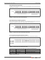
to notify the PLC that the bit 3 of the input is set to "1".
● No match between the input data mask and the input data
Step
Description
Operation
High byte
Low byte
�
Input data
Input data mask
AND operation
0110 1111
0000 0000
0000 0000
1011 0001
0000 1000
0000 0000
�
Result of the AND operation
Input data mask
XOR operation
0000 0000
0000 0000
0000 0000
0000 0000
0000 1000
0000 1000
Tab. 4-5:
Number
Xn
OFF
Example for masking input data (no match)
Description
�
A bitwise AND operation between the input data and the input data mask is performed.
쐇
A bitwise XOR operation between the result of the AND operation and the input data mask is performed.
Since a bit is set in the result of the XOR operation, the input signal Xn is switched OFF.
Tab. 4-6:
Explanation for the example
● Match between the input data mask and the input data
Step
Description
Operation
High byte
Low byte
�
Input data
Input data mask
AND operation
0111 1001
0000 0000
0000 0000
0010 1010
0000 1000
0000 1000
�
Result of the AND operation
Input data mask
XOR operation
0000 0000
0000 0000
0000 0000
0000 1000
0000 1000
0000 0000
Tab. 4-7:
Number
ON
Example for masking input data (match)
Description
�
A bitwise AND operation between the input data and the input data mask is performed.
쐇
A bitwise XOR operation the result of the AND operation and the input data mask is performed.
Since no bit is set in the result of the XOR operation, the input signal Xn is switched ON.
Tab. 4-8:
Xn
Explanation for the example
MELSEC-L series — IO-Link Master Module ME1IOL6-L
4–7
Detailed Description of the Module
Functions of the IO-Link Master Module
An input data mask is only active if their value is greater than 0.
The byte order of the process data in buffer memory can be swapped (refer to section 4.3.5). This takes
impact also on the input mask operation. When using the input mask on a channel which runs with
reverse byte order (Data align flag = "1"), the input mask should be set in reverse byte order too.
The following figure shows the mask operation and the dependency to the byte order of the input
data.
Input process
data
Data
(H) or (L)*
Data
(H) or (L)*
Fig. 4-3:
If the bits set to "1" in the input data mask are set
also in the first two bytes of the input data, the
data mask result is set to "1".
Logical operation
Input data mask
Data
(H)
Data mask result
Data
(L)
Xn
* High and low byte order depends on data align
setting.
4.3.4
Output HOLD/CLEAR Function
For the case where the programmable controller (PLC) CPU is placed in STOP or in a stop error status,
whether to hold (HOLD) or clear (CLEAR) the outputs can be set.
Make the setting in the HOLD/CLEAR setting of the intelligent function module switch (please refer to
section 5.5.2).
Switch 3 is used to define the behaviour of the
– output signals Yn1 to Yn6 (SIO output mode) and the
– output data valid signals Y(n+1)1 to Y(n+6)1 (IO-Link mode)
4–8
Functions of the IO-Link Master Module
4.3.5
Detailed Description of the Module
Data Swapping Function
This is a function to exchange (swap) the upper and lower bytes of the process data and on-requestdata (acyclic data) stored in the buffer memory of the ME1IOL6-L and the IO-Link device.
With this function, the word data processing need not swap the bytes using the sequence program for
IO-Link devices storing the data in a reversed order.
The following figure shows the data flow and the swapping functionality of the ME1IOL6-L.
Fig. 4-4:
In this figure the data swapping is activated.
Swapping of data can be enabled or disabled for each channel of the ME1IOL6-L. The function is controlled by the data align flag in the mode setting register (buffer memory addresses Un\G248 to
Un\G253, refer to section 4.5.6).
By default (Data align = 0 = Data swapping active), the contents of the high and low byte is swapped.
This operation is shown in the above figure.
If Data align is set to 1, the swapping is disabled and the byte order of the data bytes in buffer memory
will be the same as coming from the device.
MELSEC-L series — IO-Link Master Module ME1IOL6-L
4–9
Detailed Description of the Module
4.3.6
Functions of the IO-Link Master Module
Exchange of Consistent Data
To exchange more than two bytes of process data in a consistent way or to have a synchronization
between reading input data and writing output data it is necessary to use the consistency handshake
signals provided by the ME1IOL6-L.
Using these signals ensures that the master will not update the process data during reading or writing
from/to buffer memory.
The handshake signals can be used for input and output separately. The interaction of the signals is
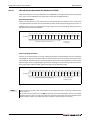
shown in the following figure.
�
�
�
�
ON
CH Output data consistency
enable flag (Un\G230)
OFF
ON
CH Data consistency start
(Y(n+1)A to Y(n+1)F)
OFF
ON
CH Consistent data available
(X(n+1)A to X(n+1)F)
OFF
Performed by the ME1IOL6-L
Fig. 4-5:
Number
Timing of the data consistency signals
Description
Input data
Output data
�
The PLC sets the CH Output data consistency start
flag and requests consistency for input data.
The CH Output data consistency enable flag is
always ON.
For each step/cycle the setting of the CH Output
data consistency start flag is required for the consistency of the output data.
쐇
The ME1IOL6-L stops updating the buffer memory.
The output of new data is stopped.
�
PLC reads inputs.
PLC can set output data.
�
ME1IOL6-L reads input data.
ME1IOL6-L sends output data.
Tab. 4-9:
Explanation for the example
Each IO-Link channel of the ME1IOL6-L can be used independently.
For requesting consistent input process data only, it is sufficient to set the concerning data consistency start signal (Y(n+1)A to Y(n+1)F) and wait until the consistent data available signal (X(n+1)A to
X(n+1)F) is turned ON.
To request the writing of consistent output data, the user has to set the output data consistency
enable flag in the buffer memory address Un\G230 (section 4.5.5). The output data from buffer memory will then be sent to the device only if the data consistency start signal (Y(n+1)A to Y(n+1)F) is
switched to ON or when the output data consistency enable flag is OFF again.
NOTE
4 – 10
If just an CH Output data consistency enable flag is set, the ME1IOL6-L will send the output data
from the buffer memory to the device once – when the CH Data consistency start signal
(Y(n+1)A to Y(n+1)F) is being set to ON. This is to ensure, that the device will get the same data as
in the buffer memory before the master signals "consistent data available".
Functions of the IO-Link Master Module
4.3.7
Detailed Description of the Module
Reading and Writing of Parameter Data
IO-Link defines service data to be exchangeable between an IO-Link device and the application. These
parameters can be indexed from 2 to 32767 and may have a length of up to 232 bytes each (index 0
and 1 is for direct parameter page addressing). The exchange of service data happens in acyclic manner on user/application demand.
Request and answer area the buffer memory
To provide this functionality to the PLC, the IO-Link Master module offers two buffer memory areas for
reading and writing those parameter record sets for each channel:
– The Acyclic Communication Request Data area (see section 4.5.14) and the
– Acyclic Communication Answer Data area (see section 4.5.17).
Both areas have some header information, followed by the parameter data. The detailed setup of the
data areas is given in the following tables.
Item
Command
Description
The type of access to a parameter (read/write).
Index
Defines the parameter to access.
Sub index
Defines the offset within the parameter.
Data size
Data
The size in bytes of the data to be
Only required in case of a
transferred.
write request.
The data to be transferred.
Setting range
Size (words)
100H to 102H
200H to 202H
301H
1
0 to 32767
1
0 to 231
1
0 to 254
1
—
128
Setting range
Size (words)
100H to 102H
200H to 202H
1
Tab. 4-10: Data required for an acyclic communication request
Item
Description
Command
The type of access to a parameter (read/write).
The data sent in the request
is returned.
Index
Defines the parameter to access.
0 to 32767
1
Sub index
Defines the offset within the
parameter
0 to 231
1
Result*
The result of the transaction
0000H to FFFFH
1
Data size*
The size in bytes of the data that was transferred.
0 to 254
1
Data*
The data that was transferred (in case of a read request).
—
128
Tab. 4-11: Data store in the acyclic communication answer areas
* If an acyclic transaction request has failed, the result area will contain an error code.
Exchange of data with an IO-Link device
A certain parameter is read from an IO-Link device by the following sequence:
햲 The sequence program writes the required data to the acyclic communication request data area
of the corresponding channel, consisting of command, parameter index and sub index.
햳 The sequence program sets the corresponding acyclic communication request flag for the channel in the buffer memory address Un\G1280 (see section 4.5.15).
햴 The IO-Link Master module performs the transfer and writes a result code into the acyclic
communication answer area. In case of a read request, the response data and the data size will
be stored also into this area.
According to the status of the communication, the ME1IOL6-L sets the corresponding acyclic
communication response flags in the buffer memory address Un\G1281 (see section 4.5.16).
MELSEC-L series — IO-Link Master Module ME1IOL6-L
4 – 11
Detailed Description of the Module
Functions of the IO-Link Master Module
The dependency of the signals and the flags is shown in the following figure.
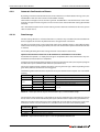
�
CH Acyclic communication
request (Un\G1280)
�
�
ON
�
�
OFF
ON
CH Acyclic communication
response: Request accepted
(Un\G1281)
OFF
ON
CH Acyclic communication
response: Request completed
(Un\G1281)
OFF
Performed by the ME1IOL6-L
Performed by the sequence program
Fig. 4-6:
Number
Timing of an acyclic communication request
Description
�
The PLC sets the request data: command, index, etc
�
The acyclic communication request for the corresponding channel is set.
�
The request is forwarded to the IO-Link device.
�
The IO-Link device responds to the request.
�
The PLC reads the answer and resets the request flag.
Tab. 4-12: Explanation for the timing shown above
The process of writing a certain parameter to an IO-Link device is done accordingly:
햲 The sequence program writes the required data to the acyclic communication request data area
of the corresponding channel, consisting of command, parameter index, sub index and data size.
햳 The sequence program writes the parameter data to the acyclic communication request data area.
햴 The sequence program sets the corresponding acyclic communication request flag for the channel in the buffer memory address Un\G1280 (see section 4.5.15).
햵 The IO-Link Master module performs the transfer to the device and writes a result code into the
acyclic communication answer area. In case of a write request, there will be no more data than
the result code in this area.
According to the status of the communication, the ME1IOL6-L sets the corresponding acyclic
communication response flags in the buffer memory address Un\G1281 (see section 4.5.16).
NOTE
4 – 12
The execution of an acyclic communication request is secured by a time-out of 60 seconds.
If within that time no response is given by the IO-Link device, the execution will be aborted. The
request completed flag will be set and the acyclic communication result area shows 1100H indicating the timeout.
Functions of the IO-Link Master Module
4.3.8
Detailed Description of the Module
Direct Parameter Page
Direct parameter page 1 (DPP1) read access
The data of parameter page 1 can be accessed by the acyclic communication function (refer to section
4.3.7) but for easier handling is also directly mapped into the buffer memory.
For each channel a direct parameter page 1 read area is reserved in the buffer memory. The IO-Link
master module reads the page from the IO-Link device and stores the 16 bytes of parameter data into
the buffer memory area. A read access is initiated by setting the direct parameter page 1 (DPP1) read
request flag.
The direct parameter page 1 (DPP1) read response flag indicates that data is available in the buffer
memory.
For a detailed information of reading the direct parameter page 1 please refer to section 4.5.18.
Direct parameter page 1 (DPP1) write access
A write access to direct parameter page 1 is not supported.
MELSEC-L series — IO-Link Master Module ME1IOL6-L
4 – 13
Detailed Description of the Module
4.3.9
Functions of the IO-Link Master Module
Automatic Confirmation of Events
By sending event data to the IO-Link master, an IO-Link device can inform about warnings, errors, etc.
The ME1IOL6-L will store these events into the buffer memory.
Some of the event types can be set to be "ignored". The ME1IOL6-L will confirm these events automatically. The type of events to ignore can be set in the event auto confirmation setting (Un\G320 to
Un\G325).
For a detailed description of the event handling and the automatic confirmation of events, please
refer to section 4.5.13.
4.3.10
Data Storage
The data storage function is a feature of IO-Link V1.1, which is only available if the connected IO-Link
device supports this function. By default the data storage function is disabled.
The data storage function can be enabled by setting the appropriate bits in the buffer memory
address for data storage setting (Un\G255). The user can select whether upload or download of data
is enabled.
The enabling/disabling of the data storage function is described in section 4.5.8.
Upload and download of data from/to IO-Link devices and deletion of stored data
Precondition for upload is an empty data storage or compatible device data. Download is only executed if the connected device is compatible.
To trigger the data exchange between the data storage and an IO-Link device, the sequence program
has to use the acyclic communication function (see section 4.3.7).
The acyclic communication command code for accessing data storage is 202H. Depending on the
given index, different commands can be triggered.
The following table shows the data required in the acyclic communication request area in the buffer
memory.
Description
Item
Contents
Meaning
Command
202H
Data storage
Code for accessing data storage
1H
Upload
Upload of parameter from IO-Link device to data storage
2H
Download
Download of parameter from data storage to IO-Link device
3H
Clear
Clear parameter data in data storage.
Sub index
—
—
Data size
—
—
Data
—
—
Index
Not used
Tab. 4-13: Data required for an acyclic communication request related to data storage
The execution of the command is requested by the acyclic communication execution flag (section
4.5.15) and the result will be reflected by the acyclic communication response flag (section 4.5.16).
When the execution of the request has been completed, the result will be stored in the acyclic communication answer area (see section 4.5.17). Possible values are shown in the following table.
Result
(hexadecimal)
Meaning
0000H
The operation was successful.
0001H
Operation failed (state conflict)
E0FFH
Invalid index, data storage is disabled
Tab. 4-14: Acyclic communication request results for upload/download/deletion
4 – 14
Functions of the IO-Link Master Module
Detailed Description of the Module
According to the acyclic communication specification, the command code and the index value will be
reflected to the answer data area. The buffer memory addresses for the sub index, the data size as well
as the data area will not contain valid data when the function returns.
Read/Write backup of data storage
Backup of data storage data is done by use of the acyclic communication. A total of 2048 bytes of
parameter data can be exchanged with the data storage. Since the buffer memory area for acyclic
communication is limited to 256 bytes, the data has to be exchanged with subsequent calls, using the
data size and the index values.
NOTE
In case of reading/writing data with sizes exceeding 256 bytes only one channel at a time can be
accessed.
● Reading of data from the data storage to the buffer memory
The command code for reading data from the data storage to the buffer memory is 200H.
The use of index 0 will start the exchange process for the whole 2048 bytes. This means that for
reading the data from the master into the buffer memory, the application has to start with a read
command with index 0. The command will return after receiving all the data from the data storage
and will present the first 256 byte in the acyclic communication answer area. Further reads with
indices 1 to 7 will then return the parameter data from byte 256 to 2048. The data size will contain
the actual amount of data in that index.
NOTE
The application can skip further reads on higher indices if the current one returned with a data
size that is smaller than 256. In this case, the rest of the parameter data is empty.
● Writing of data from the buffer memory to the data storage
The command code for writing data from the buffer memory to the data storage is 201H.
For writing the data to the data storage, the application should first fill the masters internal buffer
with the data referred by indices 1 to 7 and finally set the first 256 bytes by use of index 0: The
transfer process will start.
MELSEC-L series — IO-Link Master Module ME1IOL6-L
4 – 15
Detailed Description of the Module
4.3.11
Functions of the IO-Link Master Module
Device Validation
When the device validation is activated the ME1IOL6-L checks the connected IO-Link device at every
start-up of the IO-Link communication. In case that the validation is not successful a device error is
indicated by the ME1IOL6-L.
The device validation can be set using the acyclic communication (refer to section 4.3.7).
Two types of validation are selectable:
– Compatible device
The newly connected device must have the same vendor ID and IO-Link Device ID as the
configured device. With this setting, it is possible to replace a broken device by another device of
the same type.
– Identical device
The newly connected device must have the same vendor ID, IO-Link Device ID and serial number
as the confederated device. In other words, the same device must be connected again.
NOTE
The validation setting must be executed
– after every PLC reset or
– after every power-on of the PLC.
The following table shows the data required in the acyclic communication request area in the buffer
memory.
Description
Item
Contents
Meaning
Command
301H
Device validation
Index
1H
Code for device validation (write request)
Validation deactivated
0H
Validation type
Validation of vendor ID and IO-Link Device ID (compatible)
Validation of vendor ID, IO-Link Device ID and serial number
(identical)
2H
Sub index
—
—
—
Data size
—
—
—
Data
see table below
—
Device data
Tab. 4-15: Data required for an acyclic communication request for device validation
The following table shows the arrangement of the data in the buffer memory.
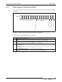
Buffer memory address*
Meaning
Hexadecimal
Decimal
High byte
Low byte
BFMH + 0000H
BFM + 0
Vendor ID 1 (MSB)
Vendor ID 2 (LSB)
BFMH + 0001H
BFM + 1
Device ID 1 (MSB)
Device ID 2
BFMH + 0002H
BFM + 2
Device ID 3 (LSB)
Serial number 1
BFMH + 0003H
BFM + 3
Serial number 2
Serial number 3
BFMH + 0004H
BFM + 4
Serial number 4
Serial number 5
BFMH + 0005H
BFM + 5
Serial number 6
Serial number 7
BFMH + 0006H
BFM + 6
Serial number 8
Serial number 9
BFMH + 0007H
BFM + 7
Serial number 10
Serial number 11
BFMH + 0008H
BFM + 8
Serial number 12
Serial number 13
BFMH + 0009H
BFM + 9
Serial number 14
Serial number 15
BFMH + 000AH
BFM + 10
Serial number 16
Reserved (Fixed to 0.)
Tab. 4-16: Storage of device data in the buffer memory
* To obtain the actual address, add the start address for the request data area of the corresponding channel.
For example, the Device ID 1 and the Device ID 2 of the device connected to channel 1 can be found in the address
Un\G420 + 1 = Un\G421.
4 – 16
Functions of the IO-Link Master Module
Detailed Description of the Module
The execution of the command is requested by the acyclic communication execution flag (section
4.5.15) and the result will be reflected by the acyclic communication response flag (section 4.5.16).
When the execution of the request has been completed, the result will be stored in the acyclic communication answer area (see section 4.5.17). Possible values are shown in the following table.
Result
(hexadecimal)
Meaning
0000H
The operation was successful.
0001H
Operation failed (state conflict)
Tab. 4-17: Acyclic communication request results for device validation
According to the acyclic communication specification, the command code and the index value will be
reflected to the answer data area. The buffer memory addresses for the sub index, the data size as well
as the data area will not contain valid data when the function returns.
MELSEC-L series — IO-Link Master Module ME1IOL6-L
4 – 17
Detailed Description of the Module
I/O Signals for the Programmable Controller CPU
4.4
I/O Signals for the Programmable Controller CPU
4.4.1
List of I/O signals
Note that the I/O numbers (X/Y) shown in this section and thereafter depends on the mounting position resp. on the start I/O number or head address of the IO-Link master module. This head address has
to be added to the shown I/O numbers.
For example, if the IO-Link master module occupies the range from X/Y040 to Y/X05F the head
address is X/Y040. However the least significant digit is omitted and the head address "n" in this case
reads as "4". The "module ready" input (Xn0) will be X40 and the "event flag" will be X50.
Signal direction CPU Module ME1IOL6-L
Device No.
Signal name
(Input)
Reference
Signal direction CPU Module ME1IOL6-L
Device No.
(Output) Signal name
Xn0
Module ready
Yn0
Use prohibited
Xn1
CH1
Yn1
CH1
Xn2
CH2
Yn2
CH2
Xn3
CH3
Yn3
CH3
Xn4
CH4
Yn4
CH4
Xn5
CH5
Yn5
CH5
Xn6
CH6
Yn6
CH6
Xn7
External power (24 V DC) ready
Yn7
Digital input
(SIO mode)
Data mask result
(IO-Link mode)
Section
4.4.2
Xn8
Yn8
Xn9
Yn9
XnA
XnB
Section
4.4.3
YnA
Use prohibited
—
YnB
XnC
YnC
XnD
YnD
XnE
Use prohibited
—
YnE
XnF
Error flag
YnF
X(n+1)0
Event flag
Y(n+1)0
X(n+1)1
CH1
X(n+1)2
CH2
X(n+1)3
CH3
X(n+1)4
CH4
X(n+1)5
X(n+1)6
Y(n+1)1
CH1
Y(n+1)2
CH2
Y(n+1)3
CH3
Y(n+1)4
CH4
CH5
Y(n+1)5
CH5
CH6
Y(n+1)6
CH6
Section
4.4.2
Input data invalid
X(n+1)7
X(n+1)8
Digital output (SIO mode)
Reference
Output data valid
Section
4.4.3
Y(n+1)7
Use prohibited
—
X(n+1)9
Y(n+1)8
Use prohibited
—
Y(n+1)9
X(n+1)A
CH1
Y(n+1)A
CH1
X(n+1)B
CH2
Y(n+1)B
CH2
X(n+1)C
CH3
X(n+1)D
CH4
Consistent data available
Section
4.4.2
Y(n+1)C
CH3
Y(n+1)D
CH4
X(n+1)E
CH5
Y(n+1)E
CH5
X(n+1)F
Ch6
Y(n+1)F
CH6
Data consistency start
Section
4.4.3
Tab. 4-18: I/O signals of the ME1IOL6-L
NOTE
4 – 18
The "Use prohibited" signals cannot be used by the user since they are for system use only.
If these signals are turned ON/OFF by the sequence program, the performance of the IO-Link master module cannot be guaranteed.
I/O Signals for the Programmable Controller CPU
4.4.2
Detailed Description of the Module
Details of Input Signals
Device No.
Signal Name
Description
Xn0
Module ready
When the programmable controller CPU is powered on or reset, this signal turns on
once the module has finished internal initialization.
When a watchdog timer error occurs, "Module ready" (X0) turns OFF.
CH digital input
(SIO mode)
The digital input value of the corresponding channel is reflected.
The signal is ON when the channel’s input is logical high.
The signal is OFF when the channel’s input is logical low.
These signal values are only valid if the external 24V supply voltage is in the specified
input range.
CH data mask
result (IO-Link
mode)
This signal represents the result of the input process data combined with the input
data mask, defined by the user (refer to section 4.3.3).
Xn1
to
Xn6
The state of the external power supply (24 V DC) is shown by signal Xn7:
The signal turns ON, 50 ms after the external power supply is turned on.
The signal turns OFF immediately after a loss of the external power supply is
detected.
The following diagram shows the timing of this signal.
Performed by the ME1IOL6-L
ON
Power supply for PLC
Xn7
ON
External power
supply READY
Module ready (Xn0)
ON
External power supply
OFF
ON
External power supply
READY (Xn7)
OFF
50 ms
XnF
Error flag
The error flag turns ON when one of the channel error flags or the module error flag
turns ON.
To turn the error flag (XnF) OFF, remove the cause of the error and confirm the error
by setting the related error reset flag in buffer memory.
X(n+1)0
Event flag
The event flag turns ON when one of the channels announces a new event.
The signal turns OFF when no un-confirmed event is pending.
X(n+1)1
to
X(n+1)6
CH input data
invalid
The channel input data invalid flag turns ON when input data (IO-Link or SIO mode)
is not updated any more.
The channel input data invalid flag turns ON when input data is marked as invalid by
the IO-Link device (IO-Link mode).
X(n+1)A
to
X(n+1)F
CH consistent
data available
In case of consistent process data access the module indicates that the process data
area in the buffer memory can be accessed. It is not updated until the "Data consistency start signal" (Y(n+1)A to Y(n+1)F) is reset by the user.
Tab. 4-19: Detailed description of the input signals (Signal direction ME1IOL6-L CPU Module)
MELSEC-L series — IO-Link Master Module ME1IOL6-L
4 – 19
Detailed Description of the Module
4.4.3
I/O Signals for the Programmable Controller CPU
Details of Output Signals
Device No.
Yn1
to
Yn6
Y(n+1)1
to
Y(n+1)6
Y(n+1)A
to
Y(n+1)F
Signal Name
Description
CH digital output (SIO mode)
Digital output signal in SIO mode.
CH output data
valid
Set this signal to ON to set the output data of the corresponding channel valid. The
logical output level of the channel will stay low as long as the Channel output data
valid flag is OFF.
NOTE: The IO-Link master will only forward this signal to the IO-Link device if it
comprises output data.
CH data
consistency start
Set this signal to exchange more than 1 word of input/ output process data in consistent manner. The module will then stop updating the input area and reading the output area for that channel and turn ON X(n+1)A to X(n+1)F to indicate consistent access
available.
When finished accessing the buffer memory, reset Y(n+1)A to Y(n+1)F to allow data
transfer.
Set the “Output Data Consistency Enable Flag” also to ON to get consistent output
process data.
For more details on consistent data exchange, please refer to section 4.3.6.
Tab. 4-20: Detailed description of the output signals (Signal direction CPU Module ME1IOL6-L)
4 – 20
Buffer Memory
4.5
Detailed Description of the Module
Buffer Memory
The ME1IOL6-L has a memory range assigned as a buffer for temporary storage of data, such as process data or error information. The PLC CPU can access this buffer and both read the stored values
from it and write new values to it which the module can then process (output values, settings for the
function of the IO-Link devices etc).
Each buffer memory address consists of 16 bits.
Bit
Buffer memory address
Fig. 4-7:
NOTE
Assignments of bits to a buffer memory address
Do not write data in the "system areas" of the buffer memory. If data is written to any of the system
areas, the PLC system may not be operated properly. Some of the user areas contain partially system areas. Care must be taken when reading/writing to the buffer memory.
Also, do not write data (e.g. in a sequence program) to the buffer memory area where writing is
disabled. Doing so may cause malfunction.
The "Default" value indicated in the following tables is the initial value set after the power is turned on
or the PLC CPU is reset.
Instructions for data exchange with the buffer memory
Communication between the PLC CPU and the buffer memory of special function modules is performed with FROM and TO instructions. The buffer memory of a special function module can also
accessed directly, e. g. with a MOV instruction.
Format of the device address: Un\Gn
– Un: Head address of the special function module
– Gn: Buffer memory address (decimal)
For example the device address U3\G11designates the buffer memory address 11 in the special function module with the head address 3 (X/Y30 to X/Y3F).
In this User's Manual the latter form of addressing is used widely.
For full documentation of all the instructions used with examples please refer to the Programming
Manual for the MELSEC System Q and the MELSEC-L series.
MELSEC-L series — IO-Link Master Module ME1IOL6-L
4 – 21
Detailed Description of the Module
4.5.1
Buffer Memory
Buffer memory assignment
Address
Hexadecimal
Decimal
0H
0
to
to
FH
15
10H
16
to
to
1FH
31
20H
32
to
to
2FH
47
30H
48
to
to
3FH
63
40H
64
to
to
4FH
79
50H
80
to
to
5FH
95
60H
96
to
to
6FH
111
70H
112
to
to
7FH
127
80H
128
to
to
8FH
143
90H
144
to
to
9FH
159
A0H
160
to
to
AFH
175
B0H
176
to
to
BFH
191
C0H
192
to
to
CFH
207
D0H
208
Description
R/W*
CH1
Input process data in IO-Link mode
0000H
R
CH2
Input process data in IO-Link mode
0000H
R
CH3
Input process data in IO-Link mode
0000H
R
Reference
Section
4.5.2
CH4
Input process data in IO-Link mode
0000H
R
CH5
Input process data in IO-Link mode
0000H
R
CH6
Input process data in IO-Link mode
0000H
R
—
—
System area
CH1
Output process data in IO-Link mode
0000H
R/W
CH2
Output process data in IO-Link mode
0000H
R/W
CH3
Output process data in IO-Link mode
0000H
R/W
—
Section
4.5.3
CH4
Output process data in IO-Link mode
0000H
R/W
CH5
Output process data in IO-Link mode
0000H
R/W
CH6
Output process data in IO-Link mode
0000H
R/W
—
—
to
to
DFH
223
System area
E0H
224
CH1
0000H
R/W
E1H
225
CH2
0000H
R/W
E2H
226
CH3
0000H
R/W
E3H
227
CH4
0000H
R/W
E4H
228
CH5
0000H
R/W
E5H
229
CH6
0000H
R/W
Input data mask
Tab. 4-21: Buffer memory assignment of the ME1IOL6-L (1/9)
* Indicates whether reading from and writing to a sequence program are enabled.
R : Read enabled
W : Write enabled
4 – 22
Default
—
Section
4.5.4
Buffer Memory
Detailed Description of the Module
Address
Hexadecimal
Decimal
E6H
230
E7H
231
Description
Output data consistency enable
System area
Default
R/W*
Reference
0000H
R/W
Section
4.5.5
—
—
—
to
to
EFH
239
F0H
240
Channel mode change flag
0000H
R/W
F1H
241
Channel mode change complete
0000H
R
F2H
242
CH1
0000H
R
F3H
243
CH2
0000H
R
F4H
244
CH3
0000H
R
F5H
245
CH4
0000H
R
F6H
246
CH5
0000H
R
F7H
247
CH6
0000H
R
F8H
248
CH1
0000H
R/W
F9H
249
CH2
0000H
R/W
0000H
R/W
0000H
R/W
Mode change result
Section
4.5.6
FAH
250
CH3
FBH
251
CH4
FCH
252
CH5
0000H
R/W
FDH
253
CH6
0000H
R/W
FEH
254
System area
—
—
—
0000H
R/W
Section
4.5.8
—
—
—
FFH
255
100H
256
Mode setting
Data storage setting
to
to
10FH
271
System area
110H
272
CH1
0000H
R
111H
273
CH2
0000H
R
112H
274
CH3
0000H
R
113H
275
CH4
0000H
R
114H
276
CH5
0000H
R
115H
277
CH6
0000H
R
116H
278
System area
—
—
—
R
Section
4.5.9
Current mode
117H
279
118H
280
Channel error flag
0000H
R
119H
281
Channel error reset flag
0000H
R/W
11AH
282
Module diagnostic information
0000H
R
Current data storage setting
0000H
11BH
283
CH1
0000H
R
11CH
284
CH2
0000H
R
11DH
285
CH3
0000H
R
11EH
286
CH4
0000H
R
Diagnostic information
11FH
287
CH5
0000H
R
120H
288
CH6
0000H
R
121H
289
to
to
13EH
318
—
—
13FH
319
System area
Section
4.5.8
Section
4.5.10
Section
4.5.11
Section
4.5.12
—
Tab. 4-22: Buffer memory assignment of the ME1IOL6-L (2/9)
* Indicates whether reading from and writing to a sequence program are enabled.
R : Read enabled
W : Write enabled
MELSEC-L series — IO-Link Master Module ME1IOL6-L
4 – 23
Detailed Description of the Module
Buffer Memory
Address
Default
R/W*
CH1
0000H
R/W
CH2
0000H
R/W
322
CH3
0000H
R/W
143H
323
CH4
0000H
R/W
144H
324
CH5
0000H
R/W
145H
325
CH6
0000H
R/W
146H
326
Event reset flag
0000H
R/W
Event flag
Hexadecimal
Decimal
140H
320
141H
321
142H
147H
327
148H
328
149H
329
14AH
330
14BH
331
to
to
14FH
335
150H
336
151H
337
152H
338
153H
339
to
to
157H
343
158H
344
159H
345
15AH
346
15BH
347
to
to
15FH
351
160H
352
161H
353
162H
354
163H
355
to
to
167H
359
168H
360
169H
361
16AH
362
16BH
363
to
to
16FH
367
170H
368
171H
369
172H
370
173H
371
to
to
19FH
415
Description
CH1
Event Auto Confirmation Setting
0000H
R
Event ID
0000H
R
Event Qualifier
0000H
R
Event Code
0000H
R
—
—
Event ID
0000H
R
Event Qualifier
0000H
R
Event Code
0000H
R
—
—
Event ID
0000H
R
Event Qualifier
0000H
R
Event Code
0000H
R
—
—
Event ID
0000H
R
Event Qualifier
0000H
R
Event Code
0000H
R
—
—
Event ID
0000H
R
Event Qualifier
0000H
R
Event Code
0000H
R
—
—
Event ID
0000H
R
Event Qualifier
0000H
R
Event Code
0000H
R
—
—
System area
CH2
System area
CH3
System area
CH4
System area
CH5
System area
CH6
System area
Tab. 4-23: Buffer memory assignment of the ME1IOL6-L (3/9)
* Indicates whether reading from and writing to a sequence program are enabled.
R : Read enabled
W : Write enabled
4 – 24
Reference
Section
4.5.13
Section
4.5.13
—
Section
4.5.13
—
Section
4.5.13
—
Section
4.5.13
—
Section
4.5.13
—
Section
4.5.13
—
Buffer Memory
Detailed Description of the Module
Address
Hexadecimal
Decimal
1A0H
416
1A1H
417
1A2H
418
1A3H
419
1A4H
420
to
to
223H
547
224H
548
Default
R/W*
Command
0000H
R/W
Index
0000H
R/W
Sub index
0000H
R/W
Data size
0000H
R/W
Data (128 words)
0000H
R/W
—
—
Description
CH1
Acyclic
communication
request
to
to
22FH
559
230H
560
Command
0000H
R/W
231H
561
Index
0000H
R/W
232H
562
Sub index
0000H
R/W
233H
563
Data size
0000H
R/W
234H
564
Data (128 words)
0000H
R/W
—
—
to
to
2B3H
691
2B4H
692
System area
CH2
Acyclic
communication
request
to
to
2BFH
703
2C0H
704
Command
0000H
R/W
2C1H
705
Index
0000H
R/W
2C2H
706
Sub index
0000H
R/W
2C3H
707
Data size
0000H
R/W
2C4H
708
Data (128 words)
0000H
R/W
—
—
to
to
343H
835
344H
836
System area
CH3
Acyclic
communication
request
to
to
34FH
847
350H
848
Command
0000H
R/W
351H
849
Index
0000H
R/W
352H
850
Sub index
0000H
R/W
353H
851
Data size
0000H
R/W
354H
852
Data (128 words)
0000H
R/W
—
—
to
to
3D3H
979
3D4H
980
System area
CH4
Acyclic
communication
request
to
to
3DFH
991
3E0H
992
Command
0000H
R/W
3E1H
993
Index
0000H
R/W
3E2H
994
Sub index
0000H
R/W
3E3H
995
Data size
0000H
R/W
3E4H
996
Data (128 words)
0000H
R/W
—
—
to
to
463H
1123
464H
1124
to
to
46FH
1135
System area
CH5
Acyclic
communication
request
System area
Reference
Section
4.5.14
—
Section
4.5.14
—
Section
4.5.14
—
Section
4.5.14
—
Section
4.5.14
—
Tab. 4-24: Buffer memory assignment of the ME1IOL6-L (4/9)
* Indicates whether reading from and writing to a sequence program are enabled.
R : Read enabled
W : Write enabled
MELSEC-L series — IO-Link Master Module ME1IOL6-L
4 – 25
Detailed Description of the Module
Buffer Memory
Address
Hexadecimal
Decimal
470H
1136
471H
1137
472H
1138
473H
1139
474H
1140
to
to
4F3H
1267
4F4H
1268
to
to
4FFH
1279
500H
1280
501H
1281
502H
1282
Default
R/W*
Command
0000H
R/W
Index
0000H
R/W
Sub index
0000H
R/W
Data size
0000H
R/W
Data (128 words)
0000H
R/W
—
—
—
Request flag
0000H
R/W
Section
4.5.15
Response flag
0000H
R
Section
4.5.16
—
—
—
Description
CH6
Acyclic
communication
request
System area
Acyclic communication
to
to
50FH
1295
510H
1296
Command
0000H
R
511H
1297
Index
0000H
R
512H
1298
Sub index
0000H
R
513H
1299
Result
0000H
R
514H
1300
Data size
0000H
R
515H
1301
Data (128 words)
0000H
R
—
—
to
to
594H
1428
595H
1429
System area
CH1
Acyclic
communication
answer
to
to
59FH
1439
5A0H
1440
Command
0000H
R
5A1H
1441
Index
0000H
R
5A2H
1442
Sub index
0000H
R
5A3H
1443
Result
0000H
R
5A4H
1444
Data size
0000H
R
5A5H
1445
Data (128 words)
0000H
R
—
—
to
to
624H
1572
625H
1573
System area
CH2
Acyclic
communication
answer
to
to
62FH
1583
630H
1584
Command
0000H
R
631H
1585
Index
0000H
R
632H
1586
Sub index
0000H
R
633H
1587
Result
0000H
R
634H
1588
Data size
0000H
R
635H
1589
Data (128 words)
0000H
R
—
—
to
to
6B4H
1716
6B5H
1717
to
to
6BFH
1727
System area
CH3
Acyclic
communication
answer
System area
Tab. 4-25: Buffer memory assignment of the ME1IOL6-L (5/9)
* Indicates whether reading from and writing to a sequence program are enabled.
R : Read enabled
W : Write enabled
4 – 26
Reference
Section
4.5.14
Section
4.5.17
—
Section
4.5.17
—
Section
4.5.17
—
Buffer Memory
Detailed Description of the Module
Address
Hexadecimal
Decimal
6C0H
1728
6C1H
1729
6C2H
1730
6C3H
1731
6C4H
1732
6C5H
1733
to
to
744H
1860
745H
1861
Default
R/W*
Command
0000H
R
Index
0000H
R
Sub index
0000H
R
Result
0000H
R
Data size
0000H
R
Data (128 words)
0000H
R
—
—
Description
CH4
Acyclic
communication
answer
to
to
74FH
1871
750H
1872
Command
0000H
R
751H
1873
Index
0000H
R
752H
1874
Sub index
0000H
R
753H
1875
Result
0000H
R
754H
1876
Data size
0000H
R
755H
1877
Data (128 words)
0000H
R
—
—
to
to
7D4H
2004
7D5H
2005
System area
CH5
Acyclic
communication
answer
to
to
7DFH
2015
7E0H
2016
Command
0000H
R
7E1H
2017
Index
0000H
R
7E2H
2018
Sub index
0000H
R
7E3H
2019
Result
0000H
R
7E4H
2020
Data size
0000H
R
7E5H
2021
Data (128 words)
0000H
R
—
—
to
to
864H
2148
865H
2149
to
to
86DH
2157
System area
CH6
Acyclic
communication
answer
System area
Reference
Section
4.5.17
—
Section
4.5.17
—
Section
4.5.17
—
Tab. 4-26: Buffer memory assignment of the ME1IOL6-L (6/9)
* Indicates whether reading from and writing to a sequence program are enabled.
R : Read enabled
W : Write enabled
MELSEC-L series — IO-Link Master Module ME1IOL6-L
4 – 27
Detailed Description of the Module
Buffer Memory
Address
Hexadecimal
Decimal
86EH
2158
86FH
2159
Default
R/W*
Reference
Read request flag
0000H
R/W
Read response flag
0000H
R
Section
4.5.18
0000H
R
Description
Direct parameter page 1
(DPP1)
High byte
Low byte
Master Cycle
Time
(Address 01H)
Master Command
(Address 00H)
870H
2160
871H
2161
F-sequence
Capability
(Address 03H)
Min. Cycle
Time
(Address 02H)
0000H
R
872H
2162
Process Data
In
(Address 05H)
IO-Link
Revision ID
(Address 04H)
0000H
R
873H
2163
Vendor ID 1
(MSB)
(Address 07H)
Process Data
Out
(Address 06H)
0000H
R
CH1
Direct parameter
page 1 (DPP1)
874H
2164
Device ID 1
(MSB)
(Address 09H)
Vendor ID 2
(LSB)
(Address 08H)
0000H
R
875H
2165
Device ID 3
(LSB)
(Address 0BH)
Device ID 2
(Address 0AH)
0000H
R
876H
2166
Function ID
(high)
(Address 0DH)
Function ID
(low)
(Address 0CH)
0000H
R
877H
2167
System
Command
(Address 0FH)
Reserved
(Address 0EH)
0000H
R
878H
2168
—
—
0000H
R
to
to
87FH
2175
880H
2176
881H
System area
High byte
Low byte
Master Cycle
Time
(Address 01H)
Master
Command
(Address 00H)
2177
F-sequence
Capability
(Address 03H)
Min. Cycle
Time
(Address 02H)
0000H
R
882H
2178
Process Data
In
(Address 05H)
IO-Link
Revision ID
(Address 04H)
0000H
R
883H
2179
Vendor ID 1
(MSB)
(Address 07H)
Process Data
Out
(Address 06H)
0000H
R
CH2
Direct parameter
page 1 (DPP1)
884H
2180
Device ID 1
(MSB)
(Address 09H)
Vendor ID 2
(LSB)
(Address 08H)
0000H
R
885H
2181
Device ID 3
(LSB)
(Address 0BH)
Device ID 2
(Address 0AH)
0000H
R
886H
2182
Function ID
(high)
(Address 0DH)
Function ID
(low)
(Address 0CH)
0000H
R
887H
2183
System
Command
(Address 0FH)
Reserved
(Address 0EH)
0000H
R
888H
2184
—
—
to
to
88FH
2191
System area
Tab. 4-27: Buffer memory assignment of the ME1IOL6-L (7/9)
* Indicates whether reading from and writing to a sequence program are enabled.
R : Read enabled
W : Write enabled
4 – 28
Section
4.5.18
—
Section
4.5.18
—
Buffer Memory
Detailed Description of the Module
Address
Hexadecimal
Decimal
Description
High byte
Low byte
Master Cycle
Time
(Address 01H)
Master
Command
(Address 00H)
Default
R/W*
0000H
R
890H
2192
891H
2193
F-sequence
Capability
(Address 03H)
Min. Cycle
Time
(Address 02H)
0000H
R
892H
2194
Process Data
In
(Address 05H)
IO-Link
Revision ID
(Address 04H)
0000H
R
893H
2195
Vendor ID 1
(MSB)
(Address 07H)
Process Data
Out
(Address 06H)
0000H
R
CH3
Direct parameter
page 1 (DPP1)
894H
2196
Device ID 1
(MSB)
(Address 09H)
Vendor ID 2
(LSB)
(Address 08H)
0000H
R
895H
2197
Device ID 3
(LSB)
(Address 0BH)
Device ID 2
(Address 0AH)
0000H
R
896H
2198
Function ID
(high)
(Address 0DH)
Function ID
(low)
(Address 0CH)
0000H
R
897H
2199
System
Command
(Address 0FH)
Reserved
(Address 0EH)
0000H
R
898H
2200
—
—
0000H
R
to
to
89FH
2207
8A0H
2208
8A1H
System area
High byte
Low byte
Master Cycle
Time
(Address 01H)
Master
Command
(Address 00H)
2209
F-sequence
Capability
(Address 03H)
Min. Cycle
Time
(Address 02H)
0000H
R
8A2H
2210
Process Data
In
(Address 05H)
IO-Link
Revision ID
(Address 04H)
0000H
R
8A3H
2211
Vendor ID 1
(MSB)
(Address 07H)
Process Data
Out
(Address 06H)
0000H
R
CH4
Direct parameter
page 1 (DPP1)
8A4H
2212
Device ID 1
(MSB)
(Address 09H)
Vendor ID 2
(LSB)
(Address 08H)
0000H
R
8A5H
2213
Device ID 3
(LSB)
(Address 0BH)
Device ID 2
(Address 0AH)
0000H
R
8A6H
2214
Function ID
(high)
(Address 0DH)
Function ID
(low)
(Address 0CH)
0000H
R
8A7H
2215
System
Command
(Address 0FH)
Reserved
(Address 0EH)
0000H
R
8A8H
2216
—
—
System area
Reference
Section
4.5.18
—
Section
4.5.18
—
Tab. 4-28: Buffer memory assignment of the ME1IOL6-L (8/9)
* Indicates whether reading from and writing to a sequence program are enabled.
R : Read enabled
W : Write enabled
MELSEC-L series — IO-Link Master Module ME1IOL6-L
4 – 29
Detailed Description of the Module
Buffer Memory
Address
Hexadecimal
Decimal
Description
High byte
Low byte
Master Cycle
Time
(Address 01H)
Master
Command
(Address 00H)
R/W*
0000H
R
8B0H
2224
8B1H
2225
F-sequence
Capability
(Address 03H)
Min. Cycle
Time
(Address 02H)
0000H
R
8B2H
2226
Process Data
In
(Address 05H)
IO-Link
Revision ID
(Address 04H)
0000H
R
8B3H
2227
Vendor ID 1
(MSB)
(Address 07H)
Process Data
Out
(Address 06H)
0000H
R
CH5
Direct parameter
page 1 (DPP1)
8B4H
2228
Device ID 1
(MSB)
(Address 09H)
Vendor ID 2
(LSB)
(Address 08H)
0000H
R
8B5H
2229
Device ID 3
(LSB)
(Address 0BH)
Device ID 2
(Address 0AH)
0000H
R
8B6H
2230
Function ID
(high)
(Address 0DH)
Function ID
(low)
(Address 0CH)
0000H
R
8B7H
2231
System
Command
(Address 0FH)
Reserved
(Address 0EH)
0000H
R
8B8H
2232
—
—
0000H
R
to
to
8BFH
2239
8C0H
2240
8C1H
System area
High byte
Low byte
Master Cycle
Time
(Address 01H)
Master
Command
(Address 00H)
2241
F-sequence
Capability
(Address 03H)
Min. Cycle
Time
(Address 02H)
0000H
R
8C2H
2242
Process Data
In
(Address 05H)
IO-Link
Revision ID
(Address 04H)
0000H
R
8C3H
2243
Vendor ID 1
(MSB)
(Address 07H)
Process Data
Out
(Address 06H)
0000H
R
CH6
Direct parameter
page 1 (DPP1)
8C4H
2244
Device ID 1
(MSB)
(Address 09H)
Vendor ID 2
(LSB)
(Address 08H)
0000H
R
8C5H
2245
Device ID 3
(LSB)
(Address 0BH)
Device ID 2
(Address 0AH)
0000H
R
8C6H
2246
Function ID
(high)
(Address 0DH)
Function ID
(low)
(Address 0CH)
0000H
R
8C7H
2247
System
Command
(Address 0FH)
Reserved
(Address 0EH)
0000H
R
8C8H
2248
—
—
to
to
7FFFH
32767
System area
Tab. 4-29: Buffer memory assignment of the ME1IOL6-L (9/9)
* Indicates whether reading from and writing to a sequence program are enabled.
R : Read enabled
W : Write enabled
4 – 30
Default
Reference
Section
4.5.18
—
Section
4.5.18
—
Buffer Memory
4.5.2
Detailed Description of the Module
CH Input Process Data (Un\G0 to Un\G15, Un\G16 to Un\G31...)
In IO-Link mode, the area of input process data reflects the current data of the connected IO-Link
device. Up to 32 bytes of input process data can be stored for each channel. The size and the structure
of the data may vary for different IO-Link device types. For that reason, the ME1IOL6-L maps the data
straight into the input process data area without any interpretation.
For the easy recognition of “high” bits in the first two bytes of the IO-Link process data the input process data bytes 1 and 2 are combined with the input data mask and form a resulting input signal for
each channel (Xn1 to Xn6). For a detailed description of the input data mask, please refer to section
4.3.3.
The input process data area will be updated every time the connected IO-Link device announces new
data to the master. Each channel's input process data area may be refreshed independently due to different cycle times of the channels.
NOTES
In IO-Link mode, the signal Xn of the channel will stay OFF if the input data mask is zero - even if
the input process data is zero too
In case that IO-Link communication stops (e.g. due to under voltage, disconnection of an IO-Link
device) the input process data buffer is set to 0.
4.5.3
CH Output Process Data (Un\G112 to Un\G127, Un\G128 to Un\G143...)
In IO-Link mode, the output process data stored in this area is output to the connected IO-Link device.
The output data size may be up to 32 bytes for each channel. The size and the structure of the data may
vary for different IO-Link device types and shall match the devices specification.
To write output data to the IO-Link device it is necessary to set the corresponding data valid signal
Y(n+1)1 to Y(n+1)6 (refer to section 4.4).
In case of a PLC stop the output data is no longer refreshed in the buffer memory. The IO-Link device
is notified by the output data valid signal (Y(n+1)1 to Y(n+1)6). The behaviour of the output data valid
signals of the ME1IOL6-L can be defined by the intelligent function module switch no. 3 (refer to section 5.5.2).
4.5.4
CH Input Data Mask (Un\G224, Un\G225 to Un\G229)
The input data mask can be used to filter the input process data for parts of special attention. Two
bytes are used to form that mask. The IO-Link master module will perform a bitwise AND operation
between the mask and the first two bytes of CH input process data (refer to section 4.5.2). The result
of that operation will be shown for each channel by the signals Xn1 to Xn6.
The CH input data mask is only active if their value is greater than 0.
For more information about the masking of input data, please refer to section 4.3.3.
MELSEC-L series — IO-Link Master Module ME1IOL6-L
4 – 31
Detailed Description of the Module
4.5.5
Buffer Memory
Output Data Consistency Enable (Un\G230)
To request the writing of consistent output data, the user has to set the output data consistency
enable flag for the corresponding channel. The output data from buffer memory will then be sent to
the device only if the Data Consistency Start signal (Y(n+1)A to Y(n+1)F) is switched to ON or when the
Output Data Consistency Enable flag is OFF again.
b15 b14 b13 b12 b11
Un\G230
0
0
0
0
0
b10
b9
b8
b7
b6
0
0
0
0
0
b5
NOTE
4.5.6
b3
b2
b1
b0
CH6 CH5 CH4 CH3 CH2 CH1
Information of b6 to b15 is fixed to 0.
Fig. 4-8:
b4
0: Data consistency disabled
1: Data consistency enabled
Assignment of the bits in buffer memory address 230
If just an Output Data Consistency Enable flag is set, the ME1IOL6-L will send the output data from
the buffer memory to the device once – when the Data Consistency Start signal (Y(n+1)A to
Y(n+1)F) is being set to ON. This is to ensure, that the device will get the same data as in the buffer
memory before the master signals "consistent data available".
Changing the Channel Mode (Un\G240 to Un\G253)
At startup all channels of the ME1IOL6-L are deactivated. The sequence program can set the channels
of the IO-Link master module to run in various modes or keep them deactivated.
The actual mode of each channel is shown in the buffer memory address for CH current mode
(Un\G272 to Un\G277, section 4.5.7).
CH Channel Mode Settings (Un\G248, Un\G249...)
The setting of the target mode is done in the buffer memory address for CH channel mode setting
(Un\G248 to Un\G253).
b15 b14 b13 b12 b11
Fig. 4-9:
4 – 32
0
0
0
0
Information of b12
to b15 is fixed to 0.
0/1
Data Align
CH1: Un\G248
CH2: Un\G249
CH3: Un\G250
CH4: Un\G251
CH5: Un\G252
CH6: Un\G253
b10
b9
0 to 7
b8
b7
b6
Time base
Mode
Assignment of the bits for the channel mode settings
b5
b4
b3
b2
b1
Multiplier (0 to 63)
Cycle Time
b0
Buffer Memory
Detailed Description of the Module
● Cycle time
The low-byte of the mode setting, which defines the cycle time, is divided in the time base and a
multiplier. The multiplier is a 6-bit factor for calculating the cycle time. Permissible values for the
multiplier are 0 to 63.
The permissible combinations for time base and multiplier are listed in the following table, along
with the resulting values for the cycle time.
Time Base
Binary code
Value
Calculation
Cycle time
b7
b6
0
0
0.1 ms
Multiplier 쎹 Time Base
0.0 ms to 6.3 ms
0
1
0.4 ms
6.4 ms 쎵 Multiplier 쎹 Time Base
6.4 ms to 31.6 ms
1
0
1.6 ms
1
1
—
32.0 ms 쎵 Multiplier 쎹 Time Base
32.0 ms to 132.8 ms
Reserved
Reserved
Tab. 4-30: Relation between time base, multiplier and cycle time
When the cycle time (bit 0 to bit 7) is set to "0" the master uses the fastest possible cycle time that
is supported by the connected IO-Link device. The cycle time is only necessary when setting a
port to IO-Link communication and should be left zero for any other mode setting.
● Mode
The mode of the channel is defined by the bits b8 to b10. Possible values for the target mode are
listed below.
Mode
Binary code
b10
b9
b8
Signal setting
Value
Description
L+첸
(L+ line)
C첸
(C/Q line)
0
0
0
0
Channel is deactivated
OFF
OFF
0
0
1
1
IO-Link mode
ON
Active
0
1
0
2
Reserved
—
—
0
1
1
3
Digital input mode (SIO mode)
ON
Active
Digital output mode (SIO mode)
ON
Active
Reserved
—
—
1
0
0
4
1
0
1
5
1
1
0
6
1
1
1
7
Tab. 4-31: Setting of modes
● Data align
Bit 11 (Data align) controls the byte order of the device data in buffer memory.
By default (Data align = 0 = Data swapping active), the byte order will be swapped.
If Data align is set to 1, the swapping is disabled and the byte order of the data bytes in buffer
memory will be the same as coming from the device.
For a detailed description of the data swapping function please refer to section 4.3.5.
NOTE
Cycle time and data align setting is only possible together with setting the IO-Link mode. During
IO-Link operation no change is possible.
MELSEC-L series — IO-Link Master Module ME1IOL6-L
4 – 33
Detailed Description of the Module
Buffer Memory
Channel Mode Change Flag (Un\G240)
To trigger the mode changing for one of the channels of the ME1IOL6-L, the user has to set the corresponding bit in Un\G240.
b15 b14 b13 b12 b11
Un\G240
0
0
0
0
0
b10
b9
b8
b7
b6
0
0
0
0
0
b5
b4
b3
b2
b1
b0
CH6 CH5 CH4 CH3 CH2 CH1
Information of b6 to b15 is fixed to 0.
0: Do not change channel mode
1: Change channel mode
Fig. 4-10: Assignment of the channel mode change flags
Channel Mode Change Complete Flag (Un\G241)
After the mode changing has been triggered by a bit in Un\G240, the IO-Link device sets the corresponding bit in Un\G241 to show that the mode change has been completed.
b15 b14 b13 b12 b11
Un\G241
0
0
0
0
0
b10
b9
b8
b7
b6
0
0
0
0
0
b5
b4
b3
b2
b1
b0
CH6 CH5 CH4 CH3 CH2 CH1
Information of b6 to b15 is fixed to 0.
0: No mode change completed
1: Mode change completed
Fig. 4-11: Assignment of the channel mode change complete flags
CH Channel Mode Change Result (Un\G242, Un\G243...)
The result of the mode change is stored separately for each channel (Un\G242 to Un\G247).
b15 b14 b13 b12 b11
b10
b9
b8
b7
b6
b5
b4
b3
b2
Change result
CH1: Un\G242
CH2: Un\G243
CH3: Un\G244
CH4: Un\G245
CH5: Un\G246
CH6: Un\G247
Fig. 4-12: Assignment of bits for the channel mode settings
Valid values for the CH Channel mode change result are shown in the following table.
Change result
Meaning
0000H
Success
—
0001H
State Conflict
Mode setting is not supported.
0002H
Wrong Cycle Time
The setting for the cycle time is invalid.
E9FFH
Time out
—
Tab. 4-32: Mode change results
4 – 34
Description
b1
b0
Buffer Memory
4.5.7
Detailed Description of the Module
CH Current Mode (Un\G272, Un\G273...)
The actual mode of each channel is shown in the buffer memory address for CH current mode
(Un\G272 to Un\G277). The format is the same as for "Mode setting" (refer to section 4.5.6).
b15 b14 b13 b12 b11
0
0
0
0
Information of b12
to b15 is fixed to 0.
b9
b8
b7
b6
b5
b4
Time base
0 to 7
0/1
Data Align
CH1: Un\G272
CH2: Un\G273
CH3: Un\G274
CH4: Un\G275
CH5: Un\G276
CH6: Un\G277
b10
b3
b2
b1
b0
Multiplier (0 to 63)
Mode
Cycle Time
Fig. 4-13: Assignment of the bits for the current channel mode
4.5.8
Data Storage Setting (Un\G255)
The data storage function (section 4.3.10) can be enabled by setting the appropriate bits in the buffer
memory address for data storage setting (Un\G255). In this buffer memory address, the user can select
whether upload or download of data is enabled or disabled.
– Upload: Transfer of parameter data from the IO-Link device to the data storage area.
– Download: Transfer of parameter data from the data storage area to the IO-Link device.
As default, both the upload and the download is disabled for all channels.
b15 b14 b13 b12 b11
Un\G255
0
0
b10
b9
b8
CH6 CH5 CH4 CH3 CH2 CH1
Fixed to 0.
Upload
b7
b6
0
0
Fixed to 0.
0: Disable upload of data
1: Enable upload of data
b5
b4
b3
b2
b1
b0
CH6 CH5 CH4 CH3 CH2 CH1
Download
0: Disable download of data
1: Enable download of data
Fig. 4-14: Assignment of the bits in buffer memory address Un\G255
MELSEC-L series — IO-Link Master Module ME1IOL6-L
4 – 35
Detailed Description of the Module
4.5.9
Buffer Memory
Current Data Storage Setting (Un\G279)
The current settings of the data storage function (section 4.3.10) can be checked in the buffer memory
address Un\G279.
Whether to enable or disable the data storing function for each channel is set in Un\G255 (please refer
to section 4.5.8).
b15 b14 b13 b12 b11
Un\G279
0
0
Fixed to 0.
b10
b9
b8
CH6 CH5 CH4 CH3 CH2 CH1
Upload*
b7
b6
0
0
b5
b4
b3
b2
b1
b0
CH6 CH5 CH4 CH3 CH2 CH1
Fixed to 0.
0: Upload of data is disabled
1: Upload of data is enabled
Download*
0: Download of data is disabled
1: Download of data is enabled
Fig. 4-15: The bits in buffer memory address Un\G279 show whether upload or download is disabled or
enabled.
* Upload:
Transfer of parameter data from the IO-Link device to the data storage.
Download: Transfer of parameter data from data storage to the IO-Link device.
4 – 36
Buffer Memory
4.5.10
Detailed Description of the Module
Channel Error Flag (Un\G280), Channel Error Reset Flag (Un\G281)
When a channel error or a module error occurs, the corresponding bit in Un\G280 is set. In addition the
error signal (XnF) will be switched ON and the LED of the corresponding channel lights up red. If the
cause of the error disappears the red LED is switched OFF and the green LED indicates the current status of the channel.
b15 b14 b13 b12 b11
Un\G280
0
0
0
0
0
b10
b9
b8
b7
0
0
0
0
b6
b5
b4
b3
b2
b1
b0
Module CH6 CH5 CH4 CH3 CH2 CH1
Information of b7 to b15 is fixed to 0.
0: No error
1: Error
Fig. 4-16: Assignment of the error flags
The error can be confirmed/reset by setting the corresponding bit in Un\G281 (Error reset) after the
cause for the error was resolved.
b15 b14 b13 b12 b11
Un\G281
0
0
0
0
0
b10
b9
b8
b7
0
0
0
0
b6
b5
b4
b3
b2
b1
b0
Module CH6 CH5 CH4 CH3 CH2 CH1
Information of b7 to b15 is fixed to 0.
0: No reset
1: Error reset
Fig. 4-17: Assignment of the error reset flags
When the error flags for all channels and the module are reset, the signal XnF will go OFF. The reset of
the error will also cause the historical channel diagnostic flags to be cleared.
The timing of the signals is shown in the following figure.
Performed by the ME1IOL6-L
Performed by the sequence program
ON
Error flag (Un\280)
OFF
ON
Error signal (XnF)
OFF
ON
Error reset flag (Un\281)
OFF
Fig. 4-18: Timing of the error flags
MELSEC-L series — IO-Link Master Module ME1IOL6-L
4 – 37
Detailed Description of the Module
4.5.11
Buffer Memory
Module diagnostic information (Un\G282)
0
0
0
0
0
b9
b8
b7
b6
b5
b4
b3
b2
b1
b0
0
0
0/1
0
0
0
0
0
0/1
0/1
0/1
24 V undervoltage
Un\G282
b10
Flash ROM access warning
b15 b14 b13 b12 b11
Flash ROM max access
In case of a module error the cause of the error is shown in the module diagnostic information register
(Un\G282).
24 V undervoltage (historic)
Information of b12 to b9 is fixed to 0.
Information of b7 to b3 is
fixed to 0.
Fig. 4-19: Assignment of the bits for the module diagnostic information
The meaning of the bits b0 to b2 and b8 is as follows:
Bit
Meaning (when bit is set to "1")
b0
External 24 V DC undervoltage
Delayed switch-on or no 24V after switch-on of the PLC are not shown as undervoltage fault.
b1
Flash ROM access warning
Excessive amount of write accesses to flash ROM (more than 250 Writes in 24h). Flash ROM write access is terminated and after module or error reset the flash ROM access is working again.
b2
The maximum number of flash ROM accesses has been reached, which is guaranteed by the flash ROM
manufacturer.
It is recommended to not use the data storage function any more or to replace the module. (This flag is not
resetable.)
The flash ROM is not accessible and the data storage function is disabled.
b8
External 24 V DC undervoltage.
The appearance of the 24 V fault is stored here until it has been confirmed by the user.
Tab. 4-33: Module diagnostic information
4 – 38
Buffer Memory
4.5.12
Detailed Description of the Module
CH Diagnostic information (Un\G283, Un\G284...)
In case of an error at a channel the cause of the error is shown in the diagnostic information register
of the corresponding channel (Un\G283 to Un\G288).
b15 b14 b13 b12 b11
b10
b9
b8
b7
b6
b5
b4
b3
b2
b1
b0
0/1
0/1
0/1
0/1
0/1
0/1
0/1
0/1
0/1
0/1
0/1
0/1
CH1: Un\G283
CH2: Un\G284
CH3: Un\G285
CH4: Un\G286
CH5: Un\G287
CH6: Un\G288
0
0/1
0/1
0/1
Historical information
Current information
Fig. 4-20: Assignment of the bits for the channel diagnostic information
The CH diagnostic information is divided into flags for the current situation and flags, describing the
historical appearance since the last error confirmation with the CH error reset flag (Un\G281). The
meaning of the bits is as follows:
Bit
Meaning (when bit is set to "1")
b0
L+ undervoltage
The voltage on the L+ line is too low.
b1
L+ overload
An overload has occurred on the L+ line.
b2
C/Q overload
An overload has occurred on the C/Q line.
b3
Overheat
The temperature is to high.
b4
Internal undervoltage fault
This fault can be caused by an undervoltage of the external 24 V DC
power supply.
b5
Device error
The IO-Link device validation is negative (refer to device validation).
The IO-Link device does not support the configured cycle time. The
cycle time setting needs to be increased.
b6
Data storage error
An error in association with the data storage function has occurred.
b7
Device connected
This bit is set to "1" when in IO-Link mode a device has been detected.
This bit is reset ("0") when a device is not present.
b8
L+ undervoltage
b9
L+ overload
b10
C/Q overload
b11
Overheat
b12
Internal undervoltage fault
b13
Device error
b14
Data storage error
b15
Fixed to 0.
Description
This is historical information. It is stored until the error has been confirmed by the user.
For a more detailed description, please refer to the description of b0 to
b6.
—
Tab. 4-34: Channel diagnostic information
MELSEC-L series — IO-Link Master Module ME1IOL6-L
4 – 39
Detailed Description of the Module
4.5.13
Buffer Memory
IO-Link event information (Un\G320 to Un\G370)
An IO-Link device can send event data to the master (ME1IOL6-L) to inform about certain states, problems, errors, etc. The ME1IOL6-L will store these events into the buffer memory.
Event flags (Un\G327)
When an event appears on one of the channels, the module will store the data of the event in the
event information area of the channel (see below) and then set the corresponding bit in Un\327 to "1".
Additionally, the signal X(n+1)0 turns ON as long as there are any events pending. The signal will turn
OFF when all events were confirmed.
b15 b14 b13 b12 b11
Un\G327
0
0
0
0
0
b10
b9
b8
b7
b6
0
0
0
0
0
b5
b4
b3
b2
b1
b0
CH6 CH5 CH4 CH3 CH2 CH1
Information of b6 to b15 is fixed to 0.
0: No event
1: New event
Fig. 4-21: Assignment of the event flags
Event reset flags (Un\G326)
The PLC has to acknowledge an event by setting the bit for the corresponding channel in Un\G326.
The ME1IOL6-L will ignore any further IO-Link events from that channel as long as the former one was
not confirmed. This behaviour is necessary to keep the data in the event information area consistent.
When no more events are pending for any channel, resetting an event reset flag to "0" will cause the
Event Signal (X(n+1)0) to turn OFF (refer to the figure on the following page).
b15 b14 b13 b12 b11
Un\G326
0
0
0
0
0
b10
b9
b8
b7
b6
0
0
0
0
0
Information of b6 to b15 is fixed to 0.
b5
b4
b3
b2
b1
b0
CH6 CH5 CH4 CH3 CH2 CH1
0: No confirmation
1: Confirm event
Fig. 4-22: Assignment of the event reset flags
NOTE
4 – 40
An event flag in Un\G327 will turn off after the corresponding event reset flag in Un\G326 has
been set to "1".
An event reset flag should be set after processing the event information stored in the buffer
memory because raising an event reset flag may cause the next event’s data to be loaded into the
buffer memory if there is any. Otherwise, the event data section will be reset to zero.
Buffer Memory
Detailed Description of the Module
The indication and confirmation of events is shown in the following figure.
Performed by the ME1IOL6-L
Performed by the sequence program
ON
OFF
CH event flag (Un\327)
ON
Please see NOTE
below.
OFF
Event signal (X(n+1)0)
ON
CH event reset flag (Un\326)
OFF
NOTE: The event signal (X(n+1)0) is only switched OFF when there are no further events pending.
Fig. 4-23: Timing of the event and event reset flags
CH Event information area (Un\G328 to Un\G330, Un\G336 to Un\G338....)
The ME1IOL6-L stores events into the CH event information area. For each channel three words are
reserved for event information, containing the detailed data of the latest event.
● Event ID
Each event is assigned an unique ID (unique within the channel)
b15 b14 b13 b12 b11
b10
b9
b8
b7
b6
b5
b4
b3
b2
b1
b0
b2
b1
b0
Event ID
CH1: Un\G328
CH2: Un\G336
CH3: Un\G344
CH4: Un\G352
CH5: Un\G360
CH6: Un\G368
Fig. 4-24: The event ID is unique within a channel.
● Event Qualifier
The contents of the event qualifier gives a detailed description of the event.
CH1: Un\G329
CH2: Un\G337
CH3: Un\G345
CH4: Un\G353
CH5: Un\G361
CH6: Un\G369
0
0
0
0
0
b10
b9
b8
0
0
0
b7
b6
b5
b4
b3
0 to 3
0 to 3
0/1
0 to 7
Mode
Type
Source
b15 b14 b13 b12 b11
Instance
Information of b12 to b15 is fixed to 0.
Fig. 4-25: Assignment of the bits for the event qualifier
MELSEC-L series — IO-Link Master Module ME1IOL6-L
4 – 41
Detailed Description of the Module
Buffer Memory
– Instance
The meaning of the value for the instance is shown in the following table:
Instance
Binary code
Value
Description
b2
b1
b0
0
0
0
0
Unknown
0
0
1
1
PL (physical layer)
0
1
0
2
DL (data layer)
0
1
1
3
AL (application layer)
1
0
0
4
Application
1
0
1
5
1
1
0
6
1
1
1
7
Invalid
Tab. 4-35: Event instances
– Source
Bit 3 = "0": Device application (remote)
Bit 3 = "1": Master application (local)
– Type
Type
Binary code
Value
Description
b5
b4
0
0
0
Invalid
0
1
1
Notification
1
0
2
Warning
1
1
3
Error
Tab. 4-36:
Event types
– Mode
Type
Binary code
4 – 42
Value
Description
b7
b6
0
0
0
Invalid
0
1
1
Event single shot
1
0
2
Event disappears (going)
1
1
3
Event appears (coming)
Tab. 4-37:
Event modes
Buffer Memory
Detailed Description of the Module
● Event code
The event code is a 16 bit value defined by the IO-Link specification and the ME1IOL6-L just
forwards it to the user as it is reported by the device. Depending on the source of the event, the
meaning of the event code is either defined in the IO-Link specification or by the vendor of the
device.
b15 b14 b13 b12 b11
b10
b9
b8
b7
b6
b5
b4
b3
b2
b1
b0
Event code
CH1: Un\G330
CH2: Un\G338
CH3: Un\G346
CH4: Un\G354
CH5: Un\G362
CH6: Un\G370
Fig. 4-26: Buffer memory addresses for the event code.
NOTE
Please refer to the IO-Link specification for a detailed explanation of the event attributes.
CH Event Auto Confirmation Setting (Un\G320, Un\G321...)
0/1
0
0
0
0
b9
b8
b7
b6
b5
b4
b3
b2
b1
b0
0
0
0
0
0
0
0
0
0/1
0/1
0/1
Error
Information of b14 to b3 is fixed to 0.
Enable auto confirmation
CH1: Un\G320
CH2: Un\G321
CH3: Un\G322
CH4: Un\G323
CH5: Un\G324
CH6: Un\G325
b10
Warning
b15 b14 b13 b12 b11
Notification
The user can specify event types to be "ignored". These events will be confirmed automatically. The
type of events to ignore can be set in the CH event auto confirmation setting.
Fig. 4-27: Assignment of the bits for the auto confirmation setting
The meaning of the bits b0 to b2 and b8 is as follows:
Bit
Meaning
b0
Auto confirmation of events of type Error
b1
Auto confirmation of events of type Warning
b2
Auto confirmation of events of type Error
b15
Enable auto confirmation
Description
"0": No auto confirmation
"1": Auto confirmation
"0": Auto confirmation is disabled for this channel.
(The bits 0 to 2 have no affect.)
"1": Auto confirmation is enabled for this channel
Tab. 4-38: Four bits are used for the setting of auto confirmation
NOTE
The activation of the auto confirmation does only affect events issued AFTER the activation. It may
be necessary to confirm an already pending event manually with the event reset flag (Un\G326).
MELSEC-L series — IO-Link Master Module ME1IOL6-L
4 – 43
Detailed Description of the Module
4.5.14
Buffer Memory
CH Acyclic Communication Request (Un\G416 to Un\G1267)
In addition to the cyclic exchanged process data, a acyclic communication between the IO-Link master and an IO-Link device is also possible (see section 4.3.7).
In the buffer memory, 132 addresses are reserved for each channel storing the data required for an
acyclic communication request:
– Command (1 word)
– Index (1 word)
– Subindex (1 word)
– Data size (1 word)
– Data (128 words)
CH Command (Un\G416, Un\G560...)
b15 b14 b13 b12 b11
b10
b9
b8
b7
b6
b5
b4
b3
b2
b1
b0
Transfer command code
CH1: Un\G416
CH2: Un\G560
CH3: Un\G704
CH4: Un\G848
CH5: Un\G992
CH6: Un\G1136
Fig. 4-28: Buffer memory addresses for the acyclic communication request command code.
The valid command codes are shown in the following table.
Command
(hexadecimal)
0100H
Read request
0101H
Write request
0102H
Command abort request
0200H
0201H
0202H
0301H
NOTE
4 – 44
Tab. 4-39:
Communication request commands
Meaning
Data read request
Data storage
Data write request
Configuration Request
Device validation (write)
Other request codes than described above will return an result code of FFFFH in the acyclic communication answer data (refer to section 4.5.17).
Buffer Memory
Detailed Description of the Module
CH Index (Un\G417, Un\G561...)
The index is used to address the parameter to access. Valid index values are 0 to 32767.
b15 b14 b13 b12 b11
b10
b9
b8
b7
b6
b5
b4
b3
b2
b1
b0
Index
CH1: Un\G417
CH2: Un\G561
CH3: Un\G705
CH4: Un\G849
CH5: Un\G993
CH6: Un\G1137
Fig. 4-29: Buffer memory addresses for the acyclic communication request index
CH Sub index (Un\G418, Un\G562...)
The sub index defines the offset within the parameter. Valid sub index values are 0 to 231.
b15 b14 b13 b12 b11
b10
b9
b8
b7
b6
b5
b4
b3
b2
b1
b0
Sub index
CH1: Un\G418
CH2: Un\G562
CH3: Un\G706
CH4: Un\G850
CH5: Un\G994
CH6: Un\G1138
Fig. 4-30: Buffer memory addresses for the sub index of the acyclic communication request
CH Data size (Un\G419, Un\G563...)
In case of a write request, the data size defines the amount of bytes to be transferred. Valid values for
the data size are 0 to 254 [bytes].
b15 b14 b13 b12 b11
CH1: Un\G419
CH2: Un\G563
CH3: Un\G707
CH4: Un\G851
CH5: Un\G995
CH6: Un\G1139
b10
b9
b8
b7
b6
b5
b4
b3
b2
b1
b0
Data size
Fig. 4-31: Buffer memory addresses for the acyclic communication request data size
MELSEC-L series — IO-Link Master Module ME1IOL6-L
4 – 45
Detailed Description of the Module
Buffer Memory
CH Data (Un\G420 to Un\G547, Un\G564 to Un\G691...)
For the data transmitted with a write request, 128 words of buffer memory are reserved for each
channel.
Address
Channel
Description
Un\G420
to
CH1
Data (128 words)
CH2
Data (128 words)
CH3
Data (128 words)
CH4
Data (128 words)
CH5
Data (128 words)
CH6
Data (128 words)
Un\G547
Un\G564
to
Un\G691
Un\G708
to
Un\G835
Un\G852
to
Un\G979
Un\G996
to
Un\G1123
Un\G1140
to
Un\G1267
4 – 46
Tab. 4-40:
Buffer memory addresses for the channel data
(acyclic communication request)
Buffer Memory
4.5.15
Detailed Description of the Module
Acyclic Communication Request Flags (Un\G1280)
To issue a request for acyclic communication (section 4.3.7) the appropriate bit in the buffer memory
address Un\G1280 must be set. Afterwards the request stored in the acyclic communication request
data area for the corresponding channel (section 4.5.14) is transmitted to the IO-Link device.
b15 b14 b13 b12 b11
Un\G1280
0
0
0
0
0
b10
b9
b8
b7
b6
0
0
0
0
0
b5
b4
b3
b2
b1
b0
CH6 CH5 CH4 CH3 CH2 CH1
Information of b6 to b15 is fixed to 0.
0: No request
1: Send request
Fig. 4-32: Assignment of the bits in buffer memory address Un\G1280
4.5.16
Acyclic Communication Response Flags (Un\G1281)
The contents of Un\G1281 shows the state of an acyclic communication request. The bits in the highbyte show that the transaction is accepted/started and the low-byte shows the completion of the
channels transaction.
b15 b14 b13 b12 b11
Un\G1281
0
0
Fixed to 0.
b10
b9
b8
CH6 CH5 CH4 CH3 CH2 CH1
Acceptance
b7
b6
0
0
b5
b4
b3
b2
b1
b0
CH6 CH5 CH4 CH3 CH2 CH1
Fixed to 0.
0: No transaction accepted/started
1: Transaction is accepted/started
Completion
0: Transaction not completed
1: Transaction is completed
Fig. 4-33: Assignment of the bits in buffer memory address Un\G1281
MELSEC-L series — IO-Link Master Module ME1IOL6-L
4 – 47
Detailed Description of the Module
4.5.17
Buffer Memory
CH Acyclic Communication Answer (Un\G1296 to Un\G2148)
In addition to the cyclic exchanged process data, acyclic communication between the IO-Link master
and an IO-Link device is also possible (section 4.3.7).
When the IO-Link master sends a request for acyclic communication to an IO-link device (refer to section 4.5.14), the device answers and the data received by the master is stored in the buffer memory.
For each channel the following area is reserved for the response data:
– Command (1 word)
– Index (1 word)
– Subindex (1 word)
– Result (1 word)
– Data size (1 word)
– Data (128 words)
CH Command (Un\G1296, Un\G1440...)
The transfer command code sent in the answer is the same as in the request area (section 4.5.14).
b15 b14 b13 b12 b11
b10
b9
b8
b7
b6
b5
b4
b3
b2
b1
b0
b1
b0
Transfer command code
CH1: Un\G1296
CH2: Un\G1440
CH3: Un\G1584
CH4: Un\G1728
CH5: Un\G1872
CH6: Un\G2016
Fig. 4-34: Buffer memory addresses for the transfer command code in the answer
CH Index (Un\G1297, Un\G1441...)
The index sent in the answer is the same as in the request area (refer to section 4.5.14).
b15 b14 b13 b12 b11
CH1: Un\G1297
CH2: Un\G1441
CH3: Un\G1585
CH4: Un\G1729
CH5: Un\G1873
CH6: Un\G2017
b10
b9
b8
b7
b6
b5
b4
b3
b2
Index
Fig. 4-35: Buffer memory addresses for the index in the acyclic communication answer
4 – 48
Buffer Memory
Detailed Description of the Module
CH Sub index (Un\G1298, Un\G1442...)
The index sent in the answer is the same as in the request area (refer to section 4.5.14).
b15 b14 b13 b12 b11
b10
b9
b8
b7
b6
b5
b4
b3
b2
b1
b0
b1
b0
Sub index
CH1: Un\G1298
CH2: Un\G1442
CH3: Un\G1586
CH4: Un\G1730
CH5: Un\G1874
CH6: Un\G2018
Fig. 4-36: Buffer memory addresses for the sub index in the acyclic communication answer
CH Result (Un\G1299, Un\G1443...)
b15 b14 b13 b12 b11
b10
b9
b8
b7
b6
b5
b4
b3
b2
Result code
CH1: Un\G1299
CH2: Un\G1443
CH3: Un\G1587
CH4: Un\G1731
CH5: Un\G1875
CH6: Un\G2019
Fig. 4-37: Buffer memory addresses for the result of the acyclic communication request.
The result of the acyclic communication request is stored as hexadecimal code.
Result
(hexadecimal)
Meaning
0000H
The operation was successful.
1100H
The operation was aborted due to time-out.
E0FFH
The operation could not be performed (channel not in IO-Link mode, invalid index etc.)
FFFFH
The requested command code is not supported.
Tab. 4-41: Acyclic communication request results
NOTE
Any other result code indicates that the request itself has been executed but there were errors on
IO-Link level. For the meaning of those result codes please refer to the IO-Link specification.
MELSEC-L series — IO-Link Master Module ME1IOL6-L
4 – 49
Detailed Description of the Module
Buffer Memory
CH Data size (Un\G1300, Un\G1444...)
In case of a read request, the data size defines the amount of bytes sent in the answer. Valid values for
the data size are 0 to 254 [bytes].
b15 b14 b13 b12 b11
b10
b9
b8
b7
b6
b5
b4
b3
b2
b1
b0
Data size
CH1: Un\G1300
CH2: Un\G1444
CH3: Un\G1588
CH4: Un\G1732
CH5: Un\G1876
CH6: Un\G2020
Fig. 4-38: Buffer memory addresses for the size of the received data
CH Data (Un\G1301 to Un\G1428, Un\G1445 to Un\G1572...)
For the data transmitted with an answer, 128 words of buffer memory are reserved for each channel.
Address
Channel
Description
Un\G1301
to
CH1
Data (128 words)
CH2
Data (128 words)
CH3
Data (128 words)
CH4
Data (128 words)
CH5
Data (128 words)
CH6
Data (128 words)
Un\G1428
Un\G1445
to
Un\G1572
Un\G1589
to
Un\G1716
Un\G1733
to
Un\G1860
Un\G1877
to
Un\G2004
Un\G2021
to
Un\G2148
4 – 50
Tab. 4-42:
Buffer memory addresses for the channel data
(acyclic communication answer)
Buffer Memory
4.5.18
Detailed Description of the Module
Direct Parameter Page 1 (DPP1) Read Access
The direct parameter page 1 (DPP1) of an IO-Link device, containing device information and data
specifications, can be directly read by the master module. The DPP1 has a size of 16 bytes.
CH Direct parameter page 1 (DPP1) read request flags (Un\G2158)
Each channel has a direct parameter page 1 read area in the buffer memory. This area can be updated
by setting the appropriate bits in the buffer memory address for direct parameter page 1 (DPP1) read
request (Un\G2158).
b15 b14 b13 b12 b11
Un\G2158
0
0
0
0
0
b10
b9
b8
b7
b6
0
0
0
0
0
b5
b4
b3
b2
b1
b0
CH6 CH5 CH4 CH3 CH2 CH1
Information of b6 to b15 is fixed to 0.
0: No read request
1: DPP1 read request
Fig. 4-39: Assignment of the bits in buffer memory address Un\G2158
CH Direct parameter page 1 (DPP1) read response flags (Un\G2159)
The direct parameter page 1 (DPP1) read response flags in Un\G2159 indicate that data is available in
the corresponding buffer memory area.
b15 b14 b13 b12 b11
Un\G2158
0
0
0
0
0
b10
b9
b8
b7
b6
0
0
0
0
0
b5
b4
b3
b2
b1
b0
CH6 CH5 CH4 CH3 CH2 CH1
Information of b6 to b15 is fixed to 0.
0: No data available
1: DPP1 data available
Fig. 4-40: Assignment of the bits in buffer memory address Un\G2159
MELSEC-L series — IO-Link Master Module ME1IOL6-L
4 – 51
Buffer Memory
MELSEC-L series — IO-Link Master Module ME1IOL6-L
Detailed Description of the Module
4 – 52
Handling Precautions
Setup and Procedures before Operation
5
Setup and Procedures before Operation
5.1
Handling Precautions
● Do not drop the module or subject it to heavy impact.
● Do not remove the PCB of the module from its case. Doing so may cause the module to fail.
● Prevent foreign matter such as dust or wire chips from entering the module. Such foreign matter
can cause a fire, failure, or malfunction.
● Before handling the module, touch a grounded metal object to discharge the static electricity
from the human body.
Failure to do so may cause the module to fail or malfunction.
● Tighten the screws such as module fixing screws within the following ranges. Loose screws may
cause short circuits, failures, or malfunctions.
Tightening torque range
Screw location
Terminal block screws (M3 screws)
0.42 to 0.58 Nm
Terminal block mounting screws (M3.5 screws)
0.66 to 0.89 Nm
Tab. 5-1: Tightening torques
5.2
Getting started
Start
Fig. 5-1:
Module mounting
Mount the ME1IOL6-L to the L series PLC.
Refer to section 5.3
Wiring
Connect the external power supply and
the IO-Link devices.
Refer to section 5.4
PLC parameter setting
Refer to section 5.5
Programming and debugging
Create and check the sequence program.
Refer to chapter 6
Function chart for the setup of an IO-Link master module ME1IOL6-L
MELSEC-L series — IO-Link Master Module ME1IOL6-L
5–1
Setup and Procedures before Operation
5.3
Installation Environment and Installation Position
Installation Environment and Installation Position
For installation environment and installation position, please refer to the User's Manual for the CPU
modules of the MELSEC-L series (Hardware design, Maintenance and Inspection).
5.3.1
Safety Precautions
Design Precautions
b
WARNING:
● Configure safety circuits external to the programmable controller to ensure that the entire
system operates safely even when a fault occurs in the external power supply or the programmable controller. Failure to do so may result in an accident due to an incorrect output or
malfunction.
– Emergency stop circuits, protection circuits, and protective interlock circuits for conflicting
operations (such as forward/reverse rotations or upper/lower limit positioning) must be
configured external to the programmable controller.
– When the programmable controller detects an abnormal condition, it stops the operation
and all outputs are:
• Turned off if the overcurrent or overvoltage protection of the power supply module is
activated.
• Held or turned off according to the parameter setting if the self-diagnostic function of the
CPU module detects an error such as a watchdog timer error.
Also, all outputs may be turned on if an error occurs in a part, such as an I/O control part,
where the CPU module cannot detect any error. To ensure safety operation in such a case,
provide a safety mechanism or a fail-safe circuit external to the programmable controller.
For a fail-safe circuit example, refer to "GENERAL SAFETY REQUIREMENTS" in the manual
"Safety Guidelines" included in the CPU module or head module.
– Outputs may remain on or off due to a failure of a component such as a relay and transistor
in an output circuit. Configure an external circuit for monitoring output signals that could
cause a serious accident.
● In an output circuit, when a load current exceeding the rated current or an overcurrent caused
by a load short-circuit flows for a long time, it may cause smoke and fire. To prevent this,
configure an external safety circuit, such as a fuse.
● Configure a circuit so that the programmable controller is turned on first and then the external power supply. If the external power supply is turned on first, an accident may occur due
to an incorrect output or malfunction.
● When changing data of a running programmable controller from a peripheral device connected to the CPU module to the running programmable controller, configure an interlock
circuit in the program to ensure that the entire system will always operate safely.
For other controls to a running programmable controller (such as program modification or
operating status change), read relevant manuals carefully and ensure the safety before the
operation.
Especially, in the case of a control from an external device to a remote programmable controller, immediate action cannot be taken for a problem on the programmable controller due
to a communication failure. To prevent this, configure an interlock circuit in the program, and
determine corrective actions to be taken between the external device and CPU module in case
of a communication failure.
5–2
Installation Environment and Installation Position
Setup and Procedures before Operation
Installation Precautions
m
DANGER:
b
WARNING:
● Cut off all phases of the power source externally before starting the installation or wiring
work.
● Use the programmable controller in an environment that meets "GENERAL SPECIFICATIONS"
in the manual "Safety Guidelines" included in the CPU module or head module. Failure to do
so may result in electric shock, fire, malfunction, or damage to or deterioration of the product.
● To interconnect modules, engage the respective connectors and securely lock the module
joint levers. Incorrect interconnection may cause malfunction, failure, or drop of the module.
● Do not directly touch any conductive parts and electronic components of the module. Doing
so can cause malfunction or failure of the module.
MELSEC-L series — IO-Link Master Module ME1IOL6-L
5–3
Setup and Procedures before Operation
5.4
Wiring
5.4.1
Wiring precautions
m
DANGER:
b
WARNING:
Wiring
● Cut off all phases of the power source externally before starting the installation or wiring
work.
● After installation and wiring, attach the included terminal cover to the module before turning
it on for operation. Failure to do so may result in electric shock.
● Check the rated voltage and terminal layout before wiring to the module, and connect the
cables correctly. Connecting a power supply with a different voltage rating or incorrect wiring
may cause a fire or failure.
● Connectors for external devices must be crimped or pressed with the tool specified by the
manufacturer, or must be correctly soldered. Incomplete connections may cause short circuit,
fire, or malfunction.
● Tighten the terminal block screw within the specified torque range. Undertightening can
cause short circuit, fire, or malfunction. Overtightening can damage the screw and/or module, resulting in drop, short circuit, fire, or malfunction.
● When disconnecting the cable from the module, do not pull the cable by the cable part. For
the cable connected to the terminal block, loosen the terminal screw. Pulling the cable connected to the module may result in malfunction or damage to the module or cable.
● Prevent foreign matter such as dust or wire chips from entering the module. Such foreign
matter can cause a fire, failure, or malfunction.
Please observe the following precautions for external wiring:
● Do not lay control lines or communication cables close to the main circuit, high-voltage power
lines, or load lines. Otherwise effects of noise or surge induction are likely to take place. Keep a
safe distance of more than 100 mm from the above when wiring.
● The FG terminal of the ME1IOL6-L must be connected to the ground certainly.
● Observe the following items for wiring the terminal block. Ignorance of these items may cause
electric shock, short circuit, disconnection, or damage of the product:
– Use solderless terminals for the connection. Twist the end of stranded wires and make sure
there are no loose wires.
– Solderless terminals with insulating sleeves cannot be used for the terminal block. Covering
the cable-connection portion of the solderless terminal with a marked tube or an insulation
tube is recommended.
– Do not solder-plate the electric wire ends.
– Connect only electric wires of regular size.
– Tightening of terminal block screws should follow the torque described on page 5.1.
– Fix the electric wires so that the terminal block and connected parts of electric wires are not
directly stressed.
5–4
Wiring
5.4.2
Setup and Procedures before Operation
External wiring
For the wiring method, and how to remove or install a terminal block, please refer to the User's Manual
for the CPU modules of the MELSEC-L series (Hardware design, Maintenance and Inspection).
Although the ME1IOL6-L is a IO-Link master module, it is possible to mix conventional devices (in SIO
mode) with IO-Link devices.
To each channel of the ME1IOL6-L one device can be connected in a point-to-point configuration.
Multidrop network connection (more than one device to one channel) is not possible.
Applicable cables
For the connection of IO-Link devices, standardized 3-conductor cables or, in the control cabinet, individual leads are used. No shield is required.
The maximum extension for each individual connection is 20 m. The resistance and the capacity of the
cable should not exceed 6 Ω resp. 3 nF.
The recommended minimum gauge values must be observed. For 20 m cable length the minimum
cross-section is 0.34 mm².
External power supply
For operation of the ME1IOL6-L, an external power supply of 24 V DC (+20%, -15%, which gives a voltage range of 20.4 to 28.8 V DC), is required.
NOTE
In order to keep the specified IO-Link output voltage levels (L+ line) the external supply voltage
must be higher than 22 V DC.
Connection of the external wiring
ME1IOL6-L
IO-Link
device
L+
L+
C/Q
C+
L–
L–
CH Enable/disable
Internal circuit
24 V DC
LED
24 V DC
24 V DC power
supply
+24V
24G
Filter
FG
Fig. 5-2:
External wiring of the ME1IOL6-L
MELSEC-L series — IO-Link Master Module ME1IOL6-L
5–5
Setup and Procedures before Operation
Wiring
Noise filter (external power supply line filter)
A noise filter is a component which has an effect on conducted noise.
Power
supply
230 V AC
ME1IOL6-L
It is not required to attach the noise filter to the external power supply line, however attaching it can
suppress more noise.
CPU
Noise filter
LAMBDA
MXB-1220-33
External
power supply
(24 V DC)
IO-Link
device
Noise filter connection
Fig. 5-3:
The precautions required when installing a noise filter are described below.
● Ground the noise filter grounding terminal to the control cabinet with the shortest wire possible.
CPU
Power
supply
CPU
ME1IOL6-L
Power
supply
ME1IOL6-L
● Do not bundle the wires on the external power supply side and ME1IOL6-L side of the noise filter.
When bundled, the external power supply side noise will be induced into the ME1IOL6-L side
wires from which the noise was filtered (refer to the below figure.).
IO-Link
device
External
power supply
(24 V DC)
Noise
Noise filter
LAMBDA
MXB-1220-33
External
power supply
(24 V DC)
Noise
Noise filter
LAMBDA
MXB-1220-33
IO-Link
device
The noise will be induced when the external power
supply side and ME1IOL6-L side wires are bundled.
Separate and lay the external power supply side
and ME1IOL6-L side wire.
Example of bad wiring
Example of good wiring
Fig. 5-4:
Precautions on noise filter
The following noise filter is recommended.
Noise filter model
MXB-1220-33
Maker
LAMBDA
Rated output
5–6
Voltage
250 V AC, 250 V DC
Current
20 A
Tab. 5-2:
Recommended noise filter
PLC Parameter Setting
5.5
Setup and Procedures before Operation
PLC Parameter Setting
In the PLC parameters the I/O assignment for the ME1IOL6-L and the HOLD/CLEAR function are set.
5.5.1
I/O assignment
Start GX Works2 and open up the project with the ME1IOL6-L. After the selection of Parameter in the
Project Navigator Window, double click on PLC parameter.
The L parameter setting window will appear. Click on the I/O Assignment tab.
Fig. 5-5:
I/O assignment setting screen
Set the following for the slot in which the ME1IOL6-L is mounted:
Type:
Select "Intelligent"
Model name:
ME1IOL6-L (Entering of the module model name is optional. The entry is used
for documentation only and has no effect on the function of the module.)
Points:
Select 32 points.
Start XY:
Start I/O number for the ME1IOL6-L. (Assigning of the I/O address is not
necessary as the address is automatically assigned by the PLC CPU.)
MELSEC-L series — IO-Link Master Module ME1IOL6-L
5–7
Setup and Procedures before Operation
5.5.2
PLC Parameter Setting
Intelligent function module switch settings
The HOLD/CLEAR setting for each channel of the ME1IOL6-L is selected by a "switch" in the PLC parameters. There are no switches at the module itself.
The intelligent function module switches are set using 16 bit data (4 hexadecimal digits).
b15 b14 b13 b12 b11
b10
Digit 4
Fig. 5-6:
b9
b8
b7
b6
Digit 3
b5
b4
b3
b2
Digit 2
b1
b0
Digit 1
Bit assignment for one switch
In the I/O assignment setting screen (section 5.5.1) click on Switch Setting to display the screen shown
below, then set the switches as required. The switches can easily be set if values are entered in hexadecimal. Change the entry format to hexadecimal and then enter the values.
Fig. 5-7:
Switch setting for intelligent function modules
When the intelligent function module switches are not set, the default value for switches 1 to 5 is
0000H.
Switch 3 is used to define the behaviour of the
– output signals Yn1 to Yn6 (SIO output mode) and the
– output data valid signals Y(n+1)1 to Y(n+6)1 (IO-Link mode).
Switch
Setting item
Switch 1
Reserved
Switch 2
Reserved
Fixed to 0H
HOLD/CLEAR function setting (CH1 to CH6)
Switch 3
b15
0
b4
b3
b2
b1
b0
HOLD/CLEAR function setting
0: CLEAR the output
1: HOLD the output
0 CH6 CH5 CH4 CH3 CH2 CH1
Switch 4
Reserved
Switch 5
Reserved
Tab. 5-3:
5–8
b6 b5
Switch settings for the ME1IOL6-L
Fixed to 0H
Setting of the IO-Link Devices
5.6
Setup and Procedures before Operation
Setting of the IO-Link Devices
For setting the parameters of the IO-Link devices, a commercially available FDT/DTM* can be used.
* FDT stands for Field Device Tool and DTM stands for Device Type Manager. FDT/DTM is a communication technique for
the manufacturer-independent configuration of field devices.
For connection to an IO-Link device, CPU port connection (USB, Ethernet) as well as Ethernet networks
can be used.
PLC CPU
ME1IOL6-L
Up to six IO-Link devices (slaves) or
conventional I/O devices
USB or Ethernet
FDT
Comm DTM
Device DTM
Fig. 5-8:
System configuration for the connection to the PLC CPU
ETHERNET
PLC CPU
ME1IOL6-L
FDT
Comm DTM
Device DTM
Fig. 5-9:
Up to six IO-Link
devices (slaves) or
conventional I/O
devices
System configuration for an Ethernet connection
● IODD (IO-Link Device Description) for each IO-Link device
Please ask the manufacturer of the IO-Link device.
MELSEC-L series — IO-Link Master Module ME1IOL6-L
5–9
Setup and Procedures before Operation
5 – 10
Setting of the IO-Link Devices
Programming Procedure
6
Programming
Programming
This chapter describes the programming of the IO-Link master module ME1IOL6-L.
NOTE
6.1
When applying any of the program examples introduced in this chapter to the actual system, verify the applicability and confirm that no problems will occur in the system control.
Programming Procedure
Create a program that will execute the data exchange with IO-Link devices in the following procedure.
Start
Initial settings for each channel
• Mode
• Data swapping
• Cycle time
Execution of acyclic communication
(parameter setting etc.) if required
Input of process data?
(Are input devices connected?)
NO
YES
Reading of input process data to PLC CPU.
Output of process data?
(Are output devices connected?)
NO
YES
Writing of output process data to ME1IOL6-L
Processing for error occurrence.
End
Fig. 6-1:
Programming procedure for the ME1IOL6-L
MELSEC-L series — IO-Link Master Module ME1IOL6-L
6–1
Programming
6.2
Example 1: Input of Process Data
Example 1: Input of Process Data
System configuration
The following figure shows the system configuration used for this example. For the sake of simplicity,
only one IO-Link device which exchanges process data with the master module is connected to the
ME1IOL6-L.
CPU module (L26CPU-BT)
Input module (LX40C6)
IO-Link master module ME1IOL6-L
Power supply
module (L61P)
End cover (L6EC)
X30 to X3F
X40 to X5F
IO-Link
device
External power supply 24 V DC
Fig. 6-2:
In this and the following examples the ME1IOL6-L is mounted to the CPU module together
with an input module.
Channel
HOLD/CLEAR function setting
CH1
CLEAR
CH4 to CH6
—
Tab. 6-1:
Conditions for the intelligent function module
switch setting
Program conditions
● CH1 is used in IO-Link mode for the input of process data (refer to sections 4.5.2 and 4.5.6.).
● In the event of a module error, a message shall be displayed on the display unit of the PLC CPU.
The error shall be reset after removal of the cause.
● A warning lamp is switched ON if the device connected to channel 1 is malfunctioning. The CH1
error shall be reset after removal of the cause.
6.2.1
Before creating a program
Perform the following steps before creating a program.
Wiring of external devices
Mount the ME1IOL6-L to the MELSEC-L series PLC and connect the external power supply and the IOLink device. For details, refer to section 5.4.2.
6–2
Example 1: Input of Process Data
Programming
Switch setting in the PLC parameters
Based on the setting conditions given on the previous page, make the switch settings for the intelligent function module in the PLC parameters. The HOLD/CLEAR setting is set to CLEAR by default.
Please note, that the switches are not stored in the module, so checking and setting of the switches
is always required even if the module was used before in an other application.
Switches 1 and 2
0
0
0
0
H
Fixed to 0H.
Switch 3
0
0
HOLD/CLEAR function setting
0
0
H
b15
b6
b5
b4
b3
b2
b1
b0
0
0
0
0
0
0
0
0
CH6 CH5 CH4 CH3 CH2 CH1
CH1 to CH6: 0 (CLEAR, default)
Fixed to 0H.
Switches 2 and 5
0
0
0
0
H
Fixed to 0H.
Fig. 6-3:
Setting of the switches 1 to 5 for this example
On the Parameter setting screen of GX Works2, select the I/O assignment tab, click Switch setting,
and make settings of the switches 1 to 5 as on the screen shown below (for details about the setting,
refer to section 5.5.2).
Fig. 6-4:
Switch setting for this example
MELSEC-L series — IO-Link Master Module ME1IOL6-L
6–3
Programming
6.2.2
Example 1: Input of Process Data
Program
For full documentation of all the instructions used with examples please refer to the Programming
Manual for the MELSEC System Q and the MELSEC-L series.
List of used devices
Device
Inputs
Outputs
X30
X40
X47
X4F
X51
Y7
Function
Error reset signal
Module ready
External power (24 V DC) ready
Error
CH1: input data invalid
Warning lamp: IO-Link error
M10
Initialization of CH1 completed without fault
M11
Error during initialization of CH1
Internal relays
D100 to D115 CH1: Input process data in IO-Link mode
Register
D120
Tab. 6-2:
CH1: Diagnostic information
Remark
LX40C6 (X30 to X3F)
ME1IOL6-L (X40 to X5F)
L26CPU-BT (Y0 to Y7)
The mode for CH1 has been
changed without fault.
An error has occurred during
mode changing for CH1.
The contents of D100 to D115
corresponds to the contents of
Un\G0 to Un\G15.
The contents of D120 corresponds to the contents of
Un\G283.
List of used devices
Program parts
● Initial settings
�
�
�
�
�
Processing at error occurrence
Fig. 6-5:
Number
The channel mode setting is performed once when X40 (Module ready) turns on.
Description
�
CH1 is set to: IO-Link mode, data swapping, fastest possible cycle time
�
The channel mode change flag of CH1 is set.
�
After the channel mode change complete flag of CH1 is set, the channel mode change flag of CH1 is reset.
�
When the result of the channel mode change for CH1 is "0" the initialization has been completed without
error. In this case M10 is set.
�
M11 (Error occurrence) is set, when the result of the channel mode change for CH1 is not "0".
�
These instructions are only executed when an error has occurred during mode changing.
Tab. 6-3:
6–4
�
Description of the program for the initial settings
Example 1: Input of Process Data
Programming
● Reading of input process data
�
Fig. 6-6:
Number
�
Tab. 6-4:
The input data is stored in the registers D100 to D115.
Description
The input process data of CH1 is moved from the buffer memory of the ME1IOL6-L to the PLC CPU when
the changing of the channel mode has been completed without an error (M10)
the IO-Link master module is ready (X40)
the external power supply (24 V DC) is ON (X47)
and the input data on CH1 is valid (X51).
Description of the program shown above
● Processing for a module error
�
Processing at error occurrence
�
Processing at error occurrence
�
Processing at error occurrence
�
�
�
�
Fig. 6-7:
Number
�
Program part for module error processing
Description
When a module error is detected (Un\G280.6), the message "ME1IOL6-L fault" is displayed on the display unit
of the CPU module.
�
�
External 24 V DC undervoltage
Processing at error occurrence
�
Flash ROM access warning
Maximum number of flash ROM accesses
�
When X30 (Error reset signal) is switched ON while the module error flag is ON, the error reset flag for a module error is set.
�
When there is no module error indicated, the error reset flag is reset.
�
Without a module error, the user message on the display unit is cleared.
Tab. 6-5:
Description of the program shown above
MELSEC-L series — IO-Link Master Module ME1IOL6-L
6–5
Programming
Example 1: Input of Process Data
● Processing for a channel error
�
Processing at error detection
�
�
�
�
Fig. 6-8:
Number
Description
�
When the error detection flag for CH1 is ON (Un\G280.0), the diagnostic information for CH1 is moved to the
register D120.
�
Processing at error detection for CH1.
�
When X30 (Error reset signal) is switched ON while the CH1 error flag is ON, the error reset flag for CH1 is set.
�
When there is no error indicated for CH1, the error reset flag is reset.
�
An module error or an error at channel 1 is indicated by a flashing lamp. SM412 is a 1 second clock signal.
Tab. 6-6:
6–6
Sequence program for error handling
Description of the program shown above
Example 2: Output of Process Data
6.3
Programming
Example 2: Output of Process Data
System configuration
In this example, data is output to an IO-Link device connected to channel 1 of a ME1IOL6-L. The same
system configuration as for example 1 is used (refer to section 6.2).
Program conditions
● CH1 is used in IO-Link mode for the output of process data (refer to section 4.5.3.).
● In the event of a module error, a message shall be displayed on the display unit of the PLC CPU.
The error shall be reset after removal of the cause.
● A warning lamp is switched ON if the device connected to channel 1 is malfunctioning. The CH1
error shall be reset after removal of the cause.
6.3.1
Before creating a program
Before creating the program, perform the steps described in section 6.2.1.
6.3.2
Program
For full documentation of all the instructions used with examples please refer to the Programming
Manual for the MELSEC System Q and the MELSEC-L series.
List of used devices
Device
Inputs
Outputs
X30
X40
X47
X4F
Y7
Y51
Function
Error reset signal
Module ready
External power (24 V DC) ready
Error
Warning lamp: IO-Link error
CH1: Output data valid
M10
Initialization of CH1 completed without fault
M11
Error during initialization of CH1
D120
CH1: Diagnostic information
Internal relays
Register
D130 to D145 CH1: Output process data in IO-Link mode
Tab. 6-7:
Remark
LX40C6 (X30 to X3F)
ME1IOL6-L (X40 to X5F)
L26CPU-BT (Y0 to Y7)
ME1IOL6-L (Y40 to Y5F)
The mode for CH1 has been
changed without fault.
An error has occurred during
mode changing for CH1.
The contents of D120 corresponds to the contents of
Un\G283.
The contents of D130 to D145 is
transferred to the buffer memory
addresses Un\G112 to Un\G127.
List of used devices
Program parts
● Initial settings
The initial settings are the same as performed for example 1 (please refer to section 6.2.2).
MELSEC-L series — IO-Link Master Module ME1IOL6-L
6–7
Programming
Example 2: Output of Process Data
● Writing of output process data
�
�
Fig. 6-9:
Number
The output data is stored in the registers D130 to D145.
Description
�
The output process data for CH1 is moved from the PLC CPU to the buffer memory of the ME1IOL6-L when
the changing of the channel mode has been completed without an error (M10)
the IO-Link master module is ready (X40)
and the external power supply (24 V DC) is ON (X47).
�
The output signal "CH1 output data valid" is turned ON when the conditions mentioned above are satisfied.
Every change of the contents of the registers D130 to D145 is reflected by the data sent to the IO-Link device.
Tab. 6-8:
Description of the program shown above
● Processing for a module error
The processing for an error of the ME1IOL6-L is the same as performed for example 1 (please refer
to section 6.2.2).
● Processing for a channel error
The processing for an error at channel 1 is the same as performed for example 1 (please refer to
section 6.2.2).
6–8
Example 3: Acyclic Communication (Reading)
6.4
Programming
Example 3: Acyclic Communication (Reading)
System configuration
In this example, data is read from an IO-Link device connected to channel 1 of a ME1IOL6-L using acyclic communication. The same system configuration as for example 1 is used (refer to section 6.2).
Program conditions
● CH1 is used in IO-Link mode (refer to section 4.5.3.).
● The header information for acyclic communication is stored in registers. This allows for an easy
change of command, index and subindex.
● The read data is transferred from the buffer memory to registers for further processing.
6.4.1
Before creating a program
Before creating the program, perform the steps described in section 6.2.1.
6.4.2
Program
For full documentation of all the instructions used with examples please refer to the Programming
Manual for the MELSEC System Q and the MELSEC-L series.
List of used devices
Device
Inputs
Internal relay
X31
X40
Function
Acyclic communication start signal
Module ready
M10
Initialization of CH1 completed without fault
D150
D151
Acyclic communication request
D152
Register
Command
Index
Sub-index
D154
D155
Acyclic communication answer Data size
Data size (Number of received data)
D156
Remainder of division operation
D1000 to D1127 Read data from the IO-Link device at CH1
Tab. 6-9:
Remark
LX40C6 (X30 to X3F)
ME1IOL6-L (X40 to X5F)
The mode for CH1 has been
changed without fault.
The header information required
for the request is stored in these
registers by instructions elsewhere in the program.
Unit: Byte
Unit: Word
Used for calculation of the data
size.
The buffer memory addresses
Un\G1301 to Un\G1428 are
reflected in D1000 to D1127.
Un\G1301 -> D1000
Un\G1302 -> D1001
....
Un\G1428 -> D1127
List of used devices for acyclic communication (reading)
Program parts
● Initial settings
The initial settings are the same as performed for example 1 (please refer to section 6.2.2).
MELSEC-L series — IO-Link Master Module ME1IOL6-L
6–9
Programming
Example 3: Acyclic Communication (Reading)
● Reading of data using acyclic communication
�
�
�
�
�
�
�
�
�
Fig. 6-10: Program sequence for acyclic communication (reading of data from the IO-Link device)
Number
�
�
�
Description
When the module is ready and the initialization of CH1 has been completed without an
error, the header information for the communication request is moved to the buffer
memory.
Index
Sub-index
�
The acyclic communication request flag for CH1 is set.
�
The number of received bytes is stored in D154. This instruction and the following instructions (� to �) are
only executed when
the acyclic communication response flag for CH1 is set (Un\G1281.0)
the acyclic communication answer area contains the same command, index and subindex as the request
the operation was successful (contents of Un\G1299 = Result = "0000H").
�
The acyclic communication request flag for CH1 is reset.
�
The data size (unit: bytes) is divided by two in order to get the data size in the unit "words"
�
If the result is an odd number (In this case, D156 contains the remainder.), "1" is added to the result. This
ensures that all data received will be transferred to the buffer memory.
�
The data received from the IO-Link device is stored in registers. The number of points is determined by the
contents of D156.
Tab. 6-10: Description of the program shown above
6 – 10
Command
Example 4: Acyclic Communication (Writing)
6.5
Programming
Example 4: Acyclic Communication (Writing)
System configuration
In this example, data is written to an IO-Link device connected to channel 1 of a ME1IOL6-L using acyclic communication. The same system configuration as for example 1 is used (refer to section 6.2).
Program conditions
● CH1 is used in IO-Link mode (refer to section 4.5.3.).
● The header information for acyclic communication is stored in registers. This allows for an easy
change of command, index, subindex, data size and data.
6.5.1
Before creating a program
Before creating the program, perform the steps described in section 6.2.1.
6.5.2
Program
For full documentation of all the instructions used with examples please refer to the Programming
Manual for the MELSEC System Q and the MELSEC-L series.
List of used devices
Device
Inputs
X32
X40
Function
Acyclic communication start signal
Module ready
Internal relay
M10
Initialization of CH1 completed without fault
D150
D151
D152
D153
Command
Index
Sub-index
Data size
The header information required
for the request is stored in these
registers by instructions elsewhere in the program.
Read to be written to the IO-Link device connected to CH1
The contents of the registers
D1200 to D1327 is transferred to
the buffer memory addresses
Un\G420 to Un\G547.
D1200 -> Un\G420
D1201 -> Un\G421
....
D1327 -> Un\G527
Acyclic communication request
Register
D1200 to D1327
Remark
LX40C6 (X30 to X3F)
ME1IOL6-L (X40 to X5F)
The mode for CH1 has been
changed without fault.
Tab. 6-11: List of used devices for acyclic communication (writing)
Program parts
● Initial settings
The initial settings are the same as performed for example 1 (please refer to section 6.2.2).
MELSEC-L series — IO-Link Master Module ME1IOL6-L
6 – 11
Programming
Example 4: Acyclic Communication (Writing)
● Writing of data using acyclic communication
�
�
�
�
�
�
�
Fig. 6-11: Program sequence for acyclic communication (reading of data from the IO-Link device)
Number
Description
�
�
�
�
Command
When the module is ready and the initialization of CH1 has been completed without an
error, the header information for the communication request is moved to the buffer
memory.
Sub-index
Data size
�
The data intended for the IO-Link device is transferred to the buffer memory.
�
The acyclic communication request flag for CH1 is set.
�
The acyclic communication request flag for CH1 is reset when
the acyclic communication response flag for CH1 is set (Un\G1281.0)
the acyclic communication answer area contains the same command, index and subindex as the request
the operation was successful (contents of Un\G1299 = Result = "0000H").
Tab. 6-12: Description of the program shown above
6 – 12
Index
Troubleshooting using the LEDs of the Module
7
Troubleshooting
Troubleshooting
The following section explains the types of errors that may occur when the IO-Link master module
ME1IOL6-L is used, and how to troubleshoot such errors.
7.1
Troubleshooting using the LEDs of the Module
This section describes the errors that can be checked with the LEDs on the front of the ME1IOL6-L.
Fig. 7-1:
LED display of the ME1IOL6-L
7.1.1
When the "RUN" LED is turned off
Check item
Corrective action
Is the power being supplied to the PLC?
Confirm that the supply voltage for the power supply module is within the rated range.
Is the capacity of the power supply module adequate?
Calculate the current consumption of the CPU module, I/O
modules and intelligent function modules to see if the
power supply capacity is adequate.
Has an error occurred in the PLC?
Confirm the error code and take corrective action (refer to
section 7.4.)
Reset the programmable controller CPU and verify that
the RUN LED is lit. If it does not light even after doing this,
the module may be malfunctioning.
Please consult your local Mitsubishi representative,
explaining the detailed description of the problem.
Is the module correctly mounted to the CPU module or to an
Check the mounting condition of the module.
other module?
Tab. 7-1:
7.1.2
When the "RUN" LED is off
When any of the LEDs "1" to "6" is off
Check item
Corrective action
Is the corresponding channel deactivated?
Check the current mode of the channel (section 4.5.7).
Is an IO-Link device connected to the corresponding channel when the channel is in IO-Link mode?
Check the connection status of the device (section 5.4.2).
In SIO mode, is the input/output signal OFF?
Check the status of the input/output signals. In SIO mode,
the LEDs 1 to 6 indicate the status of these signals. When a
LED is OFF, the corresponding signal is OFF too.
Tab. 7-2:
When any off the LED "1" to "6" is off
MELSEC-L series — IO-Link Master Module ME1IOL6-L
7–1
Troubleshooting
7.1.3
Troubleshooting using the LEDs of the Module
When any of the LEDs "1" to "6" lights red
Check item
Has an error occurred on the corresponding channel?
Tab. 7-3:
7–2
When any off the LED "1" to "6" lights red
Corrective action
Check whether the input signal XnF (Error) is ON (refer to
section 4.4).
Check the diagnostic information of the channel in the
buffer memory (refer to section 4.5.12).
Errors related to Process Data
7.2
Troubleshooting
Errors related to Process Data
Check item
Corrective action
Is 24 V DC external supply power being supplied?
Check that the external supply power terminals (terminals 16 (+24V) and17 (24G)) are supplied with a 24 V DC
voltage.
(In order to keep the specified IO-Link output voltage levels (L+ line) the external supply voltage must be higher
than 22 V DC.)
Check that the input signal Xn7 (External power ready) is
ON (refer to section 4.4).
Is the ME1IOL6-L working correctly?
Check that the input signal Xn0 (Module ready) is ON
(refer to section 4.4).
Check whether the input signal XnF (Error) is ON (refer to
section 4.4).
Check the diagnostic information for the module in the
buffer memory (refer to section 4.5.11).
Is the device correctly connected to the ME1IOL6-L?
Check the connection status of the device (section 5.4.2).
Is the connected device working correctly?
Check the device connected to the channel.
Is there any fault with the signal lines such as disconnection Check for faulty condition of the signal lines by a visual
or wire break?
check and a continuity check.
Is the CPU module in the STOP status?
Set the CPU module to the RUN status.
Is the mode set for the channel correct?
Verify the contents of the buffer memory addresses 272 to
277 (Un\G272 to Un\G277) in the monitor of GX Works2
(refer to section 4.5.7).
Has an error occurred on the corresponding channel?
Check whether the input signal XnF (Error) is ON (refer to
section 4.4).
Check the diagnostic information of the channel in the
buffer memory (refer to section 4.5.12).
What is the status of the data swapping function?
Check whether the data swapping function is activated or
deactivated according to the needs of the application (refer
to sections 4.3.5 and 4.5.7).
When Input Process Data is wrong
Is the input data being written to the buffer memory?
Verify the contents of the buffer memory addresses for
the corresponding channel in the monitor of GX Works2
(refer to section 4.5.2).
Check the device connected to the channel.
Is the input data moved from the buffer memory of the
ME1IOL6-L to the PLC CPU correctly?
Check the sequence program. Make sure that the input
data is taken out of the correct buffer memory addresses
(refer to section 4.5.2).
Check that data is not moved from different sources into
the same storage destination in the PLC CPU.
Is consistent data exchanged between an external device
and the PLC CPU?
Verify that the correct handshake of signals is executed for
the exchange of consistent data.
X(n+1)A to X(n+1)F „Consistent data available“
Y(n+1)A to Y(n+1)F "Data consistency start signal"
(Refer to sections 4.3.6 and 4.4)
When Output Process Data is wrong
Is the output data being written to the correct buffer memory addresses?
Verify the contents of the buffer memory addresses for
the corresponding channel in the monitor of GX Works2
(refer to section 4.5.3).
Check the sequence program. Make sure that the output
data is moved to the correct buffer memory addresses.
Is the signal "Channel output data valid" switched ON in
order to output the data?
Verify that after writing the output data to the buffer memory, the correspondent output signal (Y(n+1)1to Y(n+1)6) is
switched ON (refer to sections 4.3.2, 4.4 and 4.5.3).
Is consistent data exchanged between an external device
and the PLC CPU?
Verify that the correct handshake of signals is executed for
the exchange of consistent data.
Un\G230 (CH Output data consistency enable flag)
Y(n+1)A to Y(n+1)F "Data consistency start signal"
(Refer to sections 4.3.6 and 4.4)
Tab. 7-4:
NOTE
Troubleshooting for process data exchange
If the process data is not read or written after the proper corrective action is taken in accordance
with the above check item, the possible cause is a module failure. Please consult your local Mitsubishi representative, explaining the detailed description of the problem.
MELSEC-L series — IO-Link Master Module ME1IOL6-L
7–3
Troubleshooting
7.3
Errors related to Acyclic Communication
Errors related to Acyclic Communication
Check item
Corrective action
Is 24 V DC external supply power being supplied?
Check that the external supply power terminals (terminals 16 (+24V) and17 (24G)) are supplied with a 24 V DC
voltage.
(In order to keep the specified IO-Link output voltage levels (L+ line) the external supply voltage must be higher
than 22 V DC.)
Check that the input signal Xn7 (External power ready) is
ON (refer to section 4.4).
Is the ME1IOL6-L working correctly?
Check that the input signal Xn0 (Module ready) is ON
(refer to section 4.4).
Check whether the input signal XnF (Error) is ON (refer to
section 4.4).
Check the diagnostic information for the module in the
buffer memory (refer to section 4.5.11).
Is the connected device working correctly?
Check the device connected to the channel.
Is the device correctly connected to the ME1IOL6-L?
Check the connection status of the device (section 5.4.2).
Is there any fault with the signal lines such as disconnection Check for faulty condition of the signal lines by a visual
or wire break?
check and a continuity check.
Is the CPU module in the STOP status?
Set the CPU module to the RUN status.
Is the mode set for the channel correct?
Verify the contents of the buffer memory addresses 272 to
277 (Un\G272 to Un\G277) in the monitor of GX Works2
(refer to section 4.5.7).
Has an error occurred on the corresponding channel?
Check whether the input signal XnF (Error) is ON (refer to
section 4.4).
Check the diagnostic information of the channel in the
buffer memory (refer to section 4.5.12).
Is the header information for the acyclic communication
request correct?
Verify the contents of the buffer memory addresses for
the acyclic communication request in the monitor of GX
Works2 (refer to section 4.5.14).
Check the codes for the command, the index and the subindex.
When writing data, check the data size and the data.
Has the acyclic communication request flag been set?
Make sure that the acyclic communication request flag of
the corresponding channel (Un\G1280) is set after the
header information has been entered in the buffer memory
(refer to sections 4.3.7 and 4.5.15).
Is the acyclic communication response flag set?
Verify that the acyclic communication response flag
(Un\G1281) is set by the ME1IOL6-L in response of a communication request (refer to sections 4.3.7 and 4.5.16).
Is the header information sent in the answer correct?
The codes for the command, the index and the sub-index
sent in the answer should read the same as in the acyclic
communication request (refer to section 4.5.17).
Is the result code equal to 0000H?
Check the result code for the communication request. If the
result code is not equal to 0000H, an error has occurred
while performing acyclic communication (section 4.5.17).
Is the data swapping function set correctly?
Check whether the data swapping function is activated or
deactivated according to the needs of the application (refer
to sections 4.3.5 and 4.5.7).
Tab. 7-5:
7–4
Troubleshooting for acyclic communication
Checking the IO-Link Master Module Status
7.4
Troubleshooting
Checking the IO-Link Master Module Status
When the IO-Link master module detailed information is selected in the system monitor of GX Works2
(Diagnostics menu -> System Monitor), the status of the module can be checked.
Fig. 7-2:
The System Monitor displays comprehensive information of the connected PLC
For further information about a module, click on the module and then click Detailed Information (see
next page).
MELSEC-L series — IO-Link Master Module ME1IOL6-L
7–5
Troubleshooting
Checking the IO-Link Master Module Status
Fig. 7-3:
Detailed information on the selected module allow an easy and quick troubleshooting
Contents of Module‘s Detailed Information
● Module
– Module Name:
Shows the designation of the module, e.g. ME1IOL6-L
– I/O Address:
Head address of the module
– Mount Position:
Shows where in the PLC the module is mounted.
– Product information:
Serial No. of the module. The letter shows the function
version.
– Production Number
● Module Information
– Module Access:
Shows whether the module is ready or not.
– Status of external power supply: Not relevant for the ME1IOL6-L.
– Fuse blown status:
Not relevant for the ME1IOL6-L.
– Status of I/O Address Verify:
Indicates whether the parameter set module and the
installed module are identical.
– I/O Clear / Hold Settings:
Not relevant for the ME1IOL6-L.
– Noise Filter Setting, etc.:
Not relevant for the ME1IOL6-L.
● Error Display
No error codes are issued by the ME1IOL6-L.
7–6
Index
A
E
Acyclic communication
Answer area . . . . . . . . . . . . . . . . . . . . . . . . 4-48
for data storage . . . . . . . . . . . . . . . . . . . . . . 4-14
for device validation . . . . . . . . . . . . . . . . . . 4-16
Overview . . . . . . . . . . . . . . . . . . . . . . . . . . 4-11
Request area . . . . . . . . . . . . . . . . . . . . . . . . 4-44
Troubleshooting . . . . . . . . . . . . . . . . . . . . . . 7-4
Error (input signal) . . . . . . . . . . . . . . . . . . . . . . .4-19
Event
Auto confirmation setting . . . . . . . . . . . . . . .4-43
automatic confirmation (overview) . . . . . . . .4-14
indication in buffer memory . . . . . . . . . . . . .4-40
Input signal . . . . . . . . . . . . . . . . . . . . . . . . .4-19
Reset flags . . . . . . . . . . . . . . . . . . . . . . . . . .4-40
External power supply
Input signal . . . . . . . . . . . . . . . . . . . . . . . . .4-19
Noise filter . . . . . . . . . . . . . . . . . . . . . . . . . . .5-6
Specifications . . . . . . . . . . . . . . . . . . . . . . . . .4-3
Wiring . . . . . . . . . . . . . . . . . . . . . . . . . . . . . .5-5
External power supply ready (input signal) . . . . . .4-19
B
Buffer memory
Overview . . . . . . . . . . . . . . . . . . . . . . . . . . 4-22
Structure . . . . . . . . . . . . . . . . . . . . . . . . . . . 4-21
C
Channel mode
Change complete flags . . . . . . . . . . . . . . . . 4-34
Change flags . . . . . . . . . . . . . . . . . . . . . . . . 4-34
Change result . . . . . . . . . . . . . . . . . . . . . . . 4-34
Current mode . . . . . . . . . . . . . . . . . . . . . . . 4-35
Settings . . . . . . . . . . . . . . . . . . . . . . . . . . . 4-32
Consistent data
available (input signal) . . . . . . . . . . . . . . . . . 4-19
Enable flags . . . . . . . . . . . . . . . . . . . . . . . . . 4-32
Output signal . . . . . . . . . . . . . . . . . . . . . . . 4-20
Overview . . . . . . . . . . . . . . . . . . . . . . . . . . 4-10
D
Data align . . . . . . . . . . . . . . . . . . . . . . . . . . . . . 4-33
Data mask result (input signal) . . . . . . . . . . . . . . 4-19
Data storage
Current settings . . . . . . . . . . . . . . . . . . . . . 4-36
Overview . . . . . . . . . . . . . . . . . . . . . . . . . . 4-14
Settings in buffer memory . . . . . . . . . . . . . . 4-35
Data swapping
Overview . . . . . . . . . . . . . . . . . . . . . . . . . . . 4-9
Setting in buffer memory . . . . . . . . . . . . . . . 4-33
Device validation . . . . . . . . . . . . . . . . . . . . . . . . 4-16
Digital input (input signal) . . . . . . . . . . . . . . . . . 4-19
DIN rail hook . . . . . . . . . . . . . . . . . . . . . . . . . . . . 4-1
Direct parameter page
read/write access . . . . . . . . . . . . . . . . . . . . . 4-13
Reading of page 1 . . . . . . . . . . . . . . . . . . . . 4-51
MELSEC-L series — IO-Link Master Module ME1IOL6-L
H
HOLD/CLEAR function
Overview . . . . . . . . . . . . . . . . . . . . . . . . . . . .4-8
Settings with intelligent function module switches
5-8
I
Input data invalid (input signal) . . . . . . . . . . . . . .4-19
Input data mask
in buffer memory . . . . . . . . . . . . . . . . . . . . .4-31
Overview . . . . . . . . . . . . . . . . . . . . . . . . . . . .4-7
Result (input signal) . . . . . . . . . . . . . . . . . . .4-19
Input signal
CHn data mask result . . . . . . . . . . . . . . . . . .4-19
CHn digital input . . . . . . . . . . . . . . . . . . . . .4-19
Consistent data available . . . . . . . . . . . . . . .4-19
Error . . . . . . . . . . . . . . . . . . . . . . . . . . . . . .4-19
Event . . . . . . . . . . . . . . . . . . . . . . . . . . . . . .4-19
External power supply ready . . . . . . . . . . . . .4-19
Input data invalid . . . . . . . . . . . . . . . . . . . . .4-19
Module ready . . . . . . . . . . . . . . . . . . . . . . . .4-19
Intelligent function module
Parameter setting . . . . . . . . . . . . . . . . . . . . . .5-7
Setting switches . . . . . . . . . . . . . . . . . . . . . . .5-8
IO-Link
Applicable cables . . . . . . . . . . . . . . . . . . . . . .5-5
Overview . . . . . . . . . . . . . . . . . . . . . . . . . . . .1-1
IO-Link device
Validation . . . . . . . . . . . . . . . . . . . . . . . . . .4-16
I
P
IO-Link mode
Data mask result . . . . . . . . . . . . . . . . . . . . . 4-19
Input process data in buffer memory . . . . . . 4-31
Output process data in buffer memory . . . . . 4-31
Overview . . . . . . . . . . . . . . . . . . . . . . . . . . . 4-6
Process data
Troubleshooting . . . . . . . . . . . . . . . . . . . . . .7-3
L
RUN LED . . . . . . . . . . . . . . . . . . . . . . . . . . . . . . .7-1
LEDs
1 to 6 . . . . . . . . . . . . . . . . . . . . . . . . . . . . . . 7-1
for troubleshooting . . . . . . . . . . . . . . . . . . . . 7-1
Overview . . . . . . . . . . . . . . . . . . . . . . . . . . . 4-1
RUN . . . . . . . . . . . . . . . . . . . . . . . . . . . . . . . 7-1
S
M
ME1IOL6-L
Dimensions . . . . . . . . . . . . . . . . . . . . . . . . . . 4-4
I/O assignment . . . . . . . . . . . . . . . . . . . . . . . 5-7
Intelligent function module switch settings . . 5-8
LEDs . . . . . . . . . . . . . . . . . . . . . . . . . . . . . . . 4-1
Parameter setting . . . . . . . . . . . . . . . . . . . . . 5-7
Specifications . . . . . . . . . . . . . . . . . . . . . . . . 4-3
Module ready (input signal) . . . . . . . . . . . . . . . . 4-19
N
Noise filter . . . . . . . . . . . . . . . . . . . . . . . . . . . . . . 5-6
O
Output data valid (output signal) . . . . . . . . . . . . 4-20
Output signal
CHn digital output . . . . . . . . . . . . . . . . . . . . 4-20
Data consistency start . . . . . . . . . . . . . . . . . 4-20
Output data valid . . . . . . . . . . . . . . . . . . . . 4-20
II
R
SIO mode
Overview . . . . . . . . . . . . . . . . . . . . . . . . . . . .4-6
Switch settings for intelligent function module . . .5-8
System monitor . . . . . . . . . . . . . . . . . . . . . . . . . .7-5
T
Terminal block
Overview . . . . . . . . . . . . . . . . . . . . . . . . . . . .4-1
Signal layout . . . . . . . . . . . . . . . . . . . . . . . . .4-2
Troubleshooting . . . . . . . . . . . . . . . . . . . . . . . . . .7-1
Acyclic communication . . . . . . . . . . . . . . . . .7-4
Process data . . . . . . . . . . . . . . . . . . . . . . . . .7-3
W
Wiring
Connection ot external devices . . . . . . . . . . . .5-5
External power supply . . . . . . . . . . . . . . . . . .5-5
MITSUBISHI ELECTRIC
HEADQUARTERS
EUROPEAN REPRESENTATIVES
EUROPEAN REPRESENTATIVES
MITSUBISHI ELECTRIC EUROPE B.V.
EUROPE
German Branch
Gothaer Straße 8
D-40880 Ratingen
Phone: +49 (0)2102 / 486-0
Fax: +49 (0)2102 / 486-1120
MITSUBISHIELECTRICEUROPEB.V.-org.sl. CZECH REP.
Czech Branch
Avenir Business Park, Radlická 714/113a
CZ-158 00 Praha 5
Phone: +420 - 251 551 470
Fax: +420 - 251-551-471
MITSUBISHI ELECTRIC EUROPE B.V.
FRANCE
French Branch
25, Boulevard des Bouvets
F-92741 Nanterre Cedex
Phone: +33 (0)1 / 55 68 55 68
Fax: +33 (0)1 / 55 68 57 57
MITSUBISHI ELECTRIC EUROPE B.V.
IRELAND
Irish Branch
Westgate Business Park, Ballymount
IRL-Dublin 24
Phone: +353 (0)1 4198800
Fax: +353 (0)1 4198890
MITSUBISHI ELECTRIC EUROPE B.V.
ITALY
Italian Branch
Viale Colleoni 7
I-20041 Agrate Brianza (MB)
Phone: +39 039 / 60 53 1
Fax: +39 039 / 60 53 312
MITSUBISHI ELECTRIC EUROPE B.V.
POLAND
Poland Branch
Krakowska 50
PL-32-083 Balice
Phone: +48 (0)12 / 630 47 00
Fax: +48 (0)12 / 630 47 01
MITSUBISHI ELECTRIC EUROPE B.V.
RUSSIA
52, bld. 3 Kosmodamianskaya nab 8 floor
RU-115054 Мoscow
Phone: +7 495 721-2070
Fax: +7 495 721-2071
MITSUBISHI ELECTRIC EUROPE B.V.
SPAIN
Spanish Branch
Carretera de Rubí 76-80
E-08190 Sant Cugat del Vallés (Barcelona)
Phone: 902 131121 // +34 935653131
Fax: +34 935891579
MITSUBISHI ELECTRIC EUROPE B.V.
UK
UK Branch
Travellers Lane
UK-Hatfield, Herts. AL10 8XB
Phone: +44 (0)1707 / 27 61 00
Fax: +44 (0)1707 / 27 86 95
MITSUBISHI ELECTRIC CORPORATION
JAPAN
Office Tower “Z” 14 F
8-12,1 chome, Harumi Chuo-Ku
Tokyo 104-6212
Phone: +81 3 622 160 60
Fax: +81 3 622 160 75
MITSUBISHI ELECTRIC AUTOMATION, Inc.
USA
500 Corporate Woods Parkway
Vernon Hills, IL 60061
Phone: +1 847 478 21 00
Fax: +1 847 478 22 53
GEVA
AUSTRIA
Wiener Straße 89
AT-2500 Baden
Phone: +43 (0)2252 / 85 55 20
Fax: +43 (0)2252 / 488 60
TECHNIKON
BELARUS
Oktyabrskaya 19, Off. 705
BY-220030 Minsk
Phone: +375 (0)17 / 210 46 26
Fax: +375 (0)17 / 210 46 26
ESCO DRIVES & AUTOMATION
BELGIUM
Culliganlaan 3
BE-1831 Diegem
Phone: +32 (0)2 / 717 64 30
Fax: +32 (0)2 / 717 64 31
Koning & Hartman b.v.
BELGIUM
Woluwelaan 31
BE-1800 Vilvoorde
Phone: +32 (0)2 / 257 02 40
Fax: +32 (0)2 / 257 02 49
INEA RBT d.o.o.
BOSNIA AND HERZEGOVINA
Aleja Lipa 56
BA-71000 Sarajevo
Phone: +387 (0)33 / 921 164
Fax: +387 (0)33/ 524 539
AKHNATON
BULGARIA
4, Andrei Ljapchev Blvd., PO Box 21
BG-1756 Sofia
Phone: +359 (0)2 / 817 6000
Fax: +359 (0)2 / 97 44 06 1
INEA RBT d.o.o.
CROATIA
Losinjska 4 a
HR-10000 Zagreb
Phone: +385 (0)1 / 36 940 - 01/ -02/ -03
Fax: +385 (0)1 / 36 940 - 03
AutoCont C.S. s.r.o.
CZECH REPUBLIC
Technologická 374/6
CZ-708 00 Ostrava-Pustkovec
Phone: +420 595 691 150
Fax: +420 595 691 199
Beijer Electronics A/S
DENMARK
Lykkegårdsvej 17
DK-4000 Roskilde
Phone: +45 (0)46/ 75 76 66
Fax: +45 (0)46 / 75 56 26
Beijer Electronics Eesti OÜ
ESTONIA
Pärnu mnt.160i
EE-11317 Tallinn
Phone: +372 (0)6 / 51 81 40
Fax: +372 (0)6 / 51 81 49
Beijer Electronics OY
FINLAND
Peltoie 37
FIN-28400 Ulvila
Phone: +358 (0)207 / 463 540
Fax: +358 (0)207 / 463 541
UTECO
GREECE
5, Mavrogenous Str.
GR-18542 Piraeus
Phone: +30 211 / 1206 900
Fax: +30 211 / 1206 999
MELTRADE Kft.
HUNGARY
Fertő utca 14.
HU-1107 Budapest
Phone: +36 (0)1 / 431-9726
Fax: +36 (0)1 / 431-9727
Beijer Electronics SIA
LATVIA
Ritausmas iela 23
LV-1058 Riga
Phone: +371 (0)784 / 2280
Fax: +371 (0)784 / 2281
Beijer Electronics UAB
LITHUANIA
Savanoriu Pr. 187
LT-02300 Vilnius
Phone: +370 (0)5 / 232 3101
Fax: +370 (0)5 / 232 2980
ALFATRADE Ltd.
MALTA
99, Paola Hill
Malta- Paola PLA 1702
Phone: +356 (0)21 / 697 816
Fax: +356 (0)21 / 697 817
INTEHSIS srl
MOLDOVA
bld. Traian 23/1
MD-2060 Kishinev
Phone: +373 (0)22 / 66 4242
Fax: +373 (0)22 / 66 4280
HIFLEX AUTOM.TECHNIEK B.V.
NETHERLANDS
Wolweverstraat 22
NL-2984 CD Ridderkerk
Phone: +31 (0)180 – 46 60 04
Fax: +31 (0)180 – 44 23 55
Koning & Hartman b.v.
NETHERLANDS
Haarlerbergweg 21-23
NL-1101 CH Amsterdam
Phone: +31 (0)20 / 587 76 00
Fax: +31 (0)20 / 587 76 05
Beijer Electronics AS
NORWAY
Postboks 487
NO-3002 Drammen
Phone: +47 (0)32 / 24 30 00
Fax: +47 (0)32 / 84 85 77
Fonseca S.A.
PORTUGAL
R. João Francisco do Casal 87/89
PT - 3801-997 Aveiro, Esgueira
Phone: +351 (0)234 / 303 900
Fax: +351 (0)234 / 303 910
Sirius Trading & Services srl
ROMANIA
Aleea Lacul Morii Nr. 3
RO-060841 Bucuresti, Sector 6
Phone: +40 (0)21 / 430 40 06
Fax: +40 (0)21 / 430 40 02
INEA RBT d.o.o.
SERBIA
Izletnicka 10
SER-113000 Smederevo
Phone: +381 (0)26 / 615 401
Fax: +381 (0)26 / 615 401
SIMAP s.r.o.
SLOVAKIA
Jána Derku 1671
SK-911 01 Trencín
Phone: +421 (0)32 743 04 72
Fax: +421 (0)32 743 75 20
PROCONT, spol. s r.o. Prešov
SLOVAKIA
Kúpelná 1/A
SK-080 01 Prešov
Phone: +421 (0)51 7580 611
Fax: +421 (0)51 7580 650
INEA RBT d.o.o.
SLOVENIA
Stegne 11
SI-1000 Ljubljana
Phone: +386 (0)1 / 513 8116
Fax: +386 (0)1 / 513 8170
Beijer Electronics AB
SWEDEN
Box 426
SE-20124 Malmö
Phone: +46 (0)40 / 35 86 00
Fax: +46 (0)40 / 93 23 01
Omni Ray AG
SWITZERLAND
Im Schörli 5
CH-8600 Dübendorf
Phone: +41 (0)44 / 802 28 80
Fax: +41 (0)44 / 802 28 28
GTS
TURKEY
Bayraktar Bulvari Nutuk Sok. No:5
TR-34775 Yukarı Dudullu-Ümraniye-İSTANBUL
Phone: +90 (0)216 526 39 90
Fax: +90 (0)216 526 3995
CSC Automation Ltd.
UKRAINE
4-B, M. Raskovoyi St.
UA-02660 Kiev
Phone: +380 (0)44 / 494 33 55
Fax: +380 (0)44 / 494-33-66
Systemgroup
UKRAINE
2 M. Krivonosa St.
UA-03680 Kiev
Phone: +380 (0)44 / 490 92 29
Fax: +380 (0)44 / 248 88 68
EURASIAN REPRESENTATIVES
TOO Kazpromavtomatika
Ul. Zhambyla 28
KAZ-100017 Karaganda
Phone: +7 7212 / 50 10 00
Fax: +7 7212 / 50 11 50
KAZAKHSTAN
MIDDLE EAST REPRESENTATIVES
ILAN & GAVISH Ltd.
ISRAEL
24 Shenkar St., Kiryat Arie
IL-49001 Petah-Tiqva
Phone: +972 (0)3 / 922 18 24
Fax: +972 (0)3 / 924 0761
GIRIT CELADON LTD
ISRAEL
12 H'aomanut Street
IL-42505 Netanya
Phone: +972 (0)9 / 863 39 80
Fax: +972 (0)9 / 885 24 30
CEG INTERNATIONAL
LEBANON
Cebaco Center/Block A Autostrade DORA
Lebanon - Beirut
Phone: +961 (0)1 / 240 430
Fax: +961 (0)1 / 240 438
AFRICAN REPRESENTATIVE
CBI Ltd.
Private Bag 2016
ZA-1600 Isando
Phone: + 27 (0)11 / 977 0770
Fax: + 27 (0)11 / 977 0761
SOUTH AFRICA
Mitsubishi Electric Europe B.V. /// FA - European Business Group /// Gothaer Straße 8 /// D-40880 Ratingen /// Germany
Tel.: +49(0)2102-4860 /// Fax: +49(0)2102-4861120 /// [email protected] /// www.mitsubishi-automation.com