1
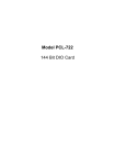
Model PCL-724
24 Bit Digital I/O Card
PCL-724 24 BIT DIGITAL I/O CARD
USER'S MANUAL
This documentation is copyrighted 1993 by Advantech
Co., Ltd. All rights are reserved. Advantech Co., Ltd.
reserves the right to make improvements in the products
described in this manual at any time without notice.
No part of this manual may be reproduced, copied,
translated or transmitted, in any form or by any means
without the prior written permission of Advantech Co.,
Ltd. Information provided in this manual is intended to
be accurate and reliable. However, Advantech Co., Ltd.
assumes no responsibility for its use, nor for any
infringements of rights of third parties which may result
from its use.
PC-LabCard is a trademark of Advantech Co., Ltd. IBM,
PC, PC/XT and PC/AT are trademarks of International
Business Machines Corporation.
OPTO-22 is a
trademark of OPTO-22 Corporation.
Part No. 2003724010 Rev.A2
Printed in Taiwan Aug. 1993
TABLE OF CONTENTS
CHAPTER 1 GENERAL INFORMATION . . . . . . . . . . . . . . .
1.1. Introduction . . . . . . . . . . . . . . . . . . . . . . . . . . . . . . . . . . .
1.2. Features . . . . . . . . . . . . . . . . . . . . . . . . . . . . . . . . . . . . . .
1.3. Applications . . . . . . . . . . . . . . . . . . . . . . . . . . . . . . . . . .
1.4. Specifications . . . . . . . . . . . . . . . . . . . . . . . . . . . . . . . . .
1
1
2
2
2
CHAPTER 2 INSTALLATION . . . . . . . . . . . . . . . . . . . . . . . . .
2.1. Initial Inspection . . . . . . . . . . . . . . . . . . . . . . . . . . . . . . .
2.2. Base Address Setting . . . . . . . . . . . . . . . . . . . . . . . . . . .
2.3. Interrupt Settings . . . . . . . . . . . . . . . . . . . . . . . . . . . . . .
5
5
6
7
CHAPTER 3 OPERATION . . . . . . . . . . . . . . . . . . . . . . . . . . .
3.1. Configuration . . . . . . . . . . . . . . . . . . . . . . . . . . . . . . . . .
3.2. Interrupt Handling . . . . . . . . . . . . . . . . . . . . . . . . . . . . .
9
9
12
CHAPTER 4 PROGRAMMING . . . . . . . . . . . . . . . . . . . . . . . .
4.1. Programming Notes . . . . . . . . . . . . . . . . . . . . . . . . . . . .
4.2. Programming Examples . . . . . . . . . . . . . . . . . . . . . . . . .
13
13
14
CHAPTER 1 GENERAL INFORMATION
1.1. Introduction
The PCL-724 24 bit DIO card is a generalized 24 line parallel digital I/O
capability, and emulates mode 0 of an 8255 programmable peripheral interface
chip. With its 50-pin, OPTO-22 compatible connector, the PCL-724 is
especially suitable for SSR I/O module control. Additionally, one line of the
PCL-724 can be used to generate a hardware interrupt to your PC.
General Information
1.2.
Features
* 24 TTL digital I/O lines, (6 connectors, each with 24 I/O lines).
*
Emulates mode O of 8255 PPI
*
Programmable interrupt handling
"
OPTO-22 compatible 50-pin connector
1.3. Applications
*
Industrial AC/DC I/O module monitoring and control
*
Relay and switch monitoring and control
*
Parallel data transfer
* Sensing the signals of TTL, DTL, CMOS logic
*
Driving indicator LED's
1.4. Electrical Specifications
Input signal
Input logic high voltage : 2.0 V -- 5.25 V
Input logic low voltage : 0.0 V -- 0.80 V
High level input current : 20.0 uA
Low level input current : - 0.2 mA
Output signal
output logic high voltage : 2.4 V (min)
output logic low voltage : 0.4 V (max)
High level output current : -15.0 mA
Low level output current : 24.0 mA
PCL-724
PCL-724
General Information
Transfer rate
Typical : 300 K bytes/sec
Maximum : 500 K bytes/sec
Power consumption
Typical power : 0.5 A @ 5V DC(+ 5%)
Maximum power : 0.8 A @ 5V DC(+ 5%)
Connector
One 50-pin connector (CN1) OPTO-22 compatible
CONNECTOR PIN ASSIGNMENT
General Information
PCL-724
If you like, you can also access the signals on CN1 by attaching connectors to
the holes in the PCB at CN2 and CN3 by yourself. The pin assignments are
as follows.
Operating environment
Temperature
Relative humidity
:
:
0 ºC to 70 ºC
5% to 90%,noncondensing
Storage environment
Temperature
Relative humidity
:
:
-55 ºC to 150 ºC
5% to 90%,noncondensing
:
:
125.0 mm by 99.5 mm
50 pin male ribbon cable connector
Dimensions
Dimensions
I/O connector
CHAPPER 2 INSTALLATION
2.1. Initial Inspection
Before installing the PCL-724 into your PC, first check to make sure that the
contents of this package include the following:
1 PCL-724 24-bit Digital I/O Card
1 User’s Manual
If anything is damaged due to shipping or appears to be defective, please
contact your local dealer.
CAUTION !
Do not install or remove the PCL-724 I/O board while the power is ON, as this
may damage the plug-in board, computer, or both. Always ensure that the
power has been turned OFF before proceeding with installation or removal.
The following diagram shows PCL-724’s switch and jumpers location
Installation
2.2.
PCL-724
Base Address Setting
The PCL-724 requires four consecutive address locations within your PC’s I/O
space. Some I/O address locations will be occupied by internal I/O and
peripherals devices. In order to avoid conflicts with these devices, the PCL724 address can be set by a 8-position DIP switch, and placed anywhere in the
IBM PC decoded external UO space. Address can range from 200 to 3FF (in
hexdecimal), though you should check with the IBM Standard Technical
Reference Manual for possible conflicts with commonly installed peripherals.
The required SWITCH settings for the BASE addresses are specified below:
---------------------------------------------------------I/O PORT
SWITCH POSITION (SW1)
ADDRESSES
1
2
3
4
5
6
7
8
(HEXADECIMAL)
A8
A7
A6 A5
A4
A3
A2
---------------------------------------------------------200 - 203
0
0
0
0
0
0
0
X
...
...
2C0 – 2C3*
0
1
1
0
0
0
0
X
...
...
3FC – 3FF
1
1
1
1
1
1
1
X
-----------------------------------------------------------
NOTE:
1.
2.
3.
4.
5.
0 = ON, 1 = OFF
“X” means “don’t care”
1..8 are switch positions
A2 through A9 correspond to address lines of the PC bus
* means factory setting
PCL-724
Installation
2.4. Interrupt Settings
The PCL-724 provides one I/O line (PCO) that generates a hardware interrupt
to your PC. The IRQ level is determined by setting jumper, J1.
(Default Setting)
The interrupt capability of PC0 is controlled by setting jumper, J2. If J2 is set
to DIS, then the interrupt capability is always disabled. Alternatively, if J2 is
set to EN, then the card's interrupt capability is always enabled. In order to
use the PCL-724's programmable interrupt feature, set J2 to PGM.
If J2 is set to PGM, I/O line, PC4, will enable the interrupt if it goes TTL
LOW . If PC4 goes TTL HIGH, then the interrupt will be disabled.
(Default Setting)
Installation
PCL-724
Set J3 to select the interrupt's trigger edge: rising or falling. See the illustration
below:
(Default Setting)
If you set the PCL-724 to trap on a rising edge change, then an interrupt will
generate if PC0 changes from TTL LOW to TTL HIGH. Conversely, if you
set the card to trap on a falling edge change, then it will generate an interrupt
when PC0 changes from TTL HIGH to LOW HIGH.
CHAPTER 3 OPERATION
The PCL-724 card emulates MODE 0 of 8255 PPI, and is pin compatible with
most industrial solid state I/O racks and modules such as those manufactured
by OPTO-22, Potter Brumfield, Gordos, etc.
The PCL-724 uses a 50-pin male IDC connectors to interface with OPTO-22
racks.
One of the PCL-724’s I/O lines (PC-0) can be used to generate a hardware
interrupt.
Note :
3.1.
The PCL-724 emulates MODE 0 of 8255 PPI, it is in effect the same
as an 8255 controller card, and all packages or programs that support
the 8255 in MODE 0 can be used on PCL-724 without reconfiguring
software.
Configuration
Mode 0 of 8255 provides simple input/output functions. No handshaking is
required since data is written directly to or read from a specified port (see 8255
MODE 0 Function Definitions).
PCL-724’s read-back function is another useful function that allows you to
monitor each output port.
8255 MODE 0 FUNCTION DEFINITIONS
−
−
−
−
−
Two 8-bit ports (Port A, Port B)
Two 4-bit ports (Port C upper, Port C lower)
Any port can be used for input or output
Outputs are latched whereas inputs are not latched
16 different input/output configurations are available in this mode.
Operation
PCL-724
Fig. 3.1
8255 address map
EXAMPLE : Base address set at 2A0
Fig. 3.2
CFG register format (mode 0)
PCL-724
Operation
The following table lists all possible configured "commands" to configure
8255 in mode 0.
8255 Mode O Configuration Table
Operation
PCL-724
3.2. Interrupt Handling
The PCL-724's I/O line, PC0, can generate a hardware interrupt to your PC.
Interrupts are edge-triggered (Please refer to Chapter 2 for the appropriate
jumper setting and description).
To use the interrupt capability via PC0 you must determine the IRQ level to be
used. Do this by simply closing the appropriate pins on J1 to select the desired
interrupt level (IRQ 2 through 7). Then close J2 to select the desired interrupt
enable mode (EN or PGM). Now, determine whether or not you want to trap
either a rising edge signal or falling edge signal change.
Note :
Since the PCL-724's digital input data are not latched, no "first
event" trapping is provided to determine which input was active
first.
Although interrupts are normally triggered by external signals, the PCL-724
can send output data to emulate an interrupt singal.
See the example in the next chapter.
CHAPTER 4 PROGRAMMING
4.1. Programming Notes
The PCL-724's signal direction can be INPUT or OUTPUT from a software
program . However, after you turn on or hardware reset your PC, all of the
PCL-724's ports will automatically be configured as INPUT.
When the PCL-724 is programmed as an output port for the first time, it will
not output until you execute the first output instruction. This action safeguards
your external device from being damaged before it is initialized,
Figure 4.1 Signal Direction of PCL-724
1.
The output driver is disabled (high impedance) when the port is set to
INPUT or after RESET.
2.
The output data written to the port is latched in the OUTPUT DATA
LATCH no matter the port is set as INPUT or OUTPUT.
3.
When the port is set as OUTPUT, the input circuit is used as output status
read-back.
4.
The data in the OUTPUT DATA LATCH is in a random status after
power on. It must be initialized before setting the port to output
direction.
Programming
PCL-724
4.2. Programming Examples
The PCL-724 is easily programmed and the following section lists some
program examples. All the program examples below have been fully tested
on PC-XT/AT or compatible computers.
Note : The following programs should be run under Turbo C version 1.5 or
2.0.
EXAMPLE 1 :
/************************************************************\
" This demo program demonstrates how to use the read back
*
* function of the PCL-724 to monitor the output status.
*
*
*
* HARDWARE SETTING :
*
*
1. Base address set at 0x2CO
*
\************************************************************/
#include
#include
#include
#include
main()
int
int
int
int
int
<stdio.h>
<conio.h>
<process.h>
<dos.h>
base = 0x2c0; /* set base address at 2CO
portA;
/" save read back value of
portB;
/* save read back value of
portC;
/* save read back value of
i,j;
/* screen handle x/
clrscr();
gotoxy(30,3);
textattr(0x70);
cputs("PCL-724 DEMO PROGRAME");
gotoxy(l1,6);
printf("Port A output value --> ");
gotoxy(l1,8);
printf("Port B output value --> ");
gotoxy(l1,10);
printf("Port C output value --> ");
gotoxy(50,6);
printf("ReadBack -->");
gotoxy(50,8);
printf("ReadBack -->");
gotoxy(50,10);
printf("ReadBack -->");
(in hex) */
port A
*/
port B
*/
port C
*/
PCL-724
/* Initialization */
outportb (0x2c3, 0x80);
Programming
/* all as output */
/********************** main program ***********************/
for(j=0;j<0x100;j++)
{
outportb ( base, j); /* out j to port A */
gotoxy(34,6);
printf("%2x",j);
portA = inportb (base);
/" read back */
gotoxy(63,6);
printf("%2x",portA);
if ( portA != j)
{
printf("\7");
/* beep */
gotoxy(30,13);
textattr(0x09);
cprintf("Port A readback error!");
getch();
exit(l);
/* quit to dos */
}
outportb ( base+1, j); /* out j to port B */
gotoxy(34,8);
printf("%2x",j);
portB = inportb (base+1);
/" read back */
gotoxy(63,8);
printf("%2x",portB);
if ( portB != j)
{
printf("\7");
/* beep */
gotoxy(30,13);
textattr(0x09);
cprintf("Port B readback error!");
getch();
exit(l);
/* quit to dos */
}
outportb ( base+2, j); /* out j to port C */
gotoxy(34,10);
printf("%2x",j);
portC = inportb (base+2);
/" read back */
gotoxy(63,10);
printf("%2x",portC);
if ( portC != j)
{
printf("\7");
/* beep */
gotoxy(30,13);
textattr(0x09);
cprintf("Port C readback error!");
getch();
exit(l);
/* quit to dos */
}
}
}
Programming
PCL-724
EXAMPLE 2 :
/*************************************************************\
* This demo program demonstrates how to use the PCL-724’s
*
* interrupt function (trapping a rising edge).
*
*
*
* HARDWARE SETTING :
*
*
1. Base address set at 0X2C0
*
*
2. J1 set at IRQ 2
*
*
3. J2 set at EN or PGM
*
*
4. J3 set at RISING trigger
*
\*************************************************************/
#include <dos.h>
#include <stdio.h>
#include <conio.h>
/* new INT OAH ISR */
void interrupt alarm (void)
{
char Port61_Old_Status;
char Port61_New_Status;
int DelayTime = 0x300;
int Count = 0;
int i;
/**
get original port 61H status, and save it
**/
Port61_New_Status = Port61_Old_Status = inportb(0x61);
/**
set port 61h bitl = '0'
Port61_New_Status &= Oxfd;
**/
/* 1111 1101 in binary */
for ( Count=O ; Count<0x300 ; Count++ , DelayTime--)
{
Port61_New_Status ^= 0x02;
/* On/Off bitl */
outportb (0x61 , Port61_New_Status);
for (i=O ; i<DelayTime ; i++);
}
outportb (0x61 , Port6l_Old_Status);
outportb (0x20, 0x20);
/* send EOI to 8259 */
}
void main()
{
int IMR;
void interrupt (*Int_A_Old_Vector)();
Int_A_Old_Vector = getvect(0x0a);
/* get old int Oah ISR */
setvet (OxOa , alarm);
/* set new int Oah ISR */
Programming
IMR = inportb(0x21);
PCL-724
/* get 8259 interrupt mask register */
/* initialization */
outportb (0x2c3 , 0x80);
/* set Port A, Port B and Port C */
/* all as output ports
*/
outportb (0x2c0, OxO);
outportb (0x2cl, OxO);
outportb (0x2c2 , 0x0);
/*
/*
/*
/*
Port A */
Port B */
PC-4=O-->interrupt enable */
PCO=O
*/
clrscr();
printf("Press any key to generate a rising edge interrupt");
getch();
outportb(0x21,0xfb & IMR);
/* set IRQ2 nonmasked */
printf("\n\nPort C = %x",inportb(0x2c2));
/* generate a rising edge signal at PCO */
outportb (0x2c2 , 0x1);
printf("\n\nPort C = %x",inportb(0x2c2));
printf("\n\npress any key to quit...");
getch();
/" restore old INT OAH ISR */
setvect (OxOa , Int_A_Old_Vector);
outportb(Ox21,IMR);
/* restore 8259 interrupt mask */
/* set as INPUT to release IRQ2 line */
outportb(0x2c3,0x9b);
}