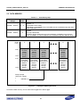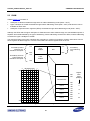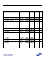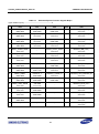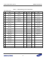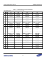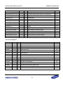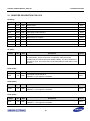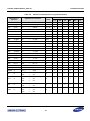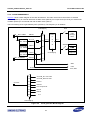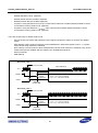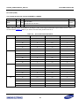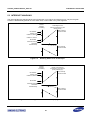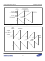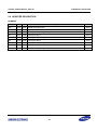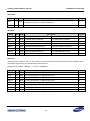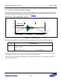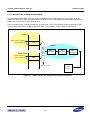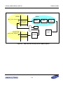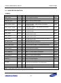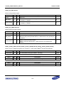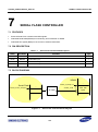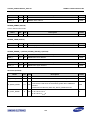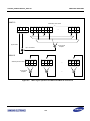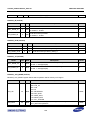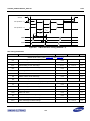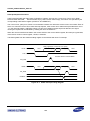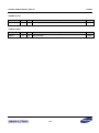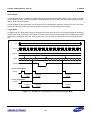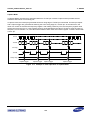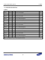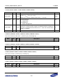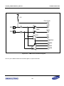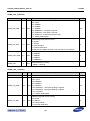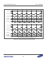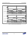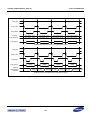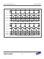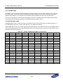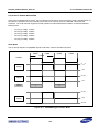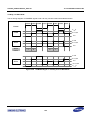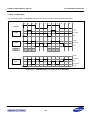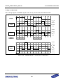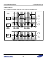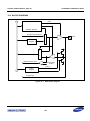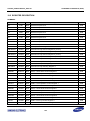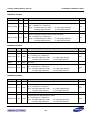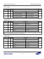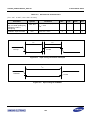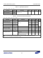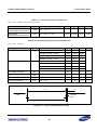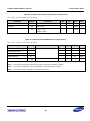
1
Rev. 0.0, Jan.2009 S3FI1BG 8-bit CMOS Microcontroller Revision 1.00 Aug 2010 User's Manual 2010 Samsung Electronics Co., Ltd. All rights reserved. Rev. 0.0, Jan.2009 Important Notice The information in this publication has been carefully checked and is believed to be entirely accurate at the time of publication. Samsung assumes no responsibility, however, for possible errors or omissions, or for any consequences resulting from the use of the information contained herein. Samsung reserves the right to make changes in its products or product specifications with the intent to improve function or design at any time and without notice and is not required to update this documentation to reflect such changes. This publication does not convey to a purchaser of semiconductor devices described herein any license under the patent rights of Samsung or others. Samsung makes no warranty, representation, or guarantee regarding the suitability of its products for any particular purpose, nor does Samsung assume any liability arising out of the application or use of any product or circuit and specifically disclaims any and all liability, including without limitation any consequential or incidental damages. "Typical" parameters can and do vary in different applications. All operating parameters, including "Typicals" must be validated for each customer application by the customer's technical experts. Samsung products are not designed, intended, or authorized for use as components in systems intended for surgical implant into the body, for other applications intended to support or sustain life, or for any other application in which the failure of the Samsung product could create a situation where personal injury or death may occur. Should the Buyer purchase or use a Samsung product for any such unintended or unauthorized application, the Buyer shall indemnify and hold Samsung and its officers, employees, subsidiaries, affiliates, and distributors harmless against all claims, costs, damages, expenses, and reasonable attorney fees arising out of, either directly or indirectly, any claim of personal injury or death that may be associated with such unintended or unauthorized use, even if such claim alleges that Samsung was negligent regarding the design or manufacture of said product. S3FI1BG 8-bit CMOS Microcontroller User's Manual, Revision 1.00 Copyright 2010 Samsung Electronics Co., Ltd. All rights reserved. No part of this publication may be reproduced, stored in a retrieval system, or transmitted in any form or by any means, electric or mechanical, by photocopying, recording, or otherwise, without the prior written consent of Samsung Electronics. Samsung Electronics Co., Ltd. San #24 Nongseo-Dong, Giheung-Gu Yongin-City, Gyeonggi-Do, Korea 446-711 Contact Us: [email protected] TEL: (82)-(31)-209-3107 FAX: (82)-(31)-209-3262 Home Page: http://www.samsungsemi.com Printed in the Republic of Korea Rev. 0.0, Jan.2009 Revision History Revision No. Date 1.00 Aug 4, 2010 Description - Initial draft Author(s) Rev. 0.0, Jan.2009 Table of Contents 1 Introduction ................................................................................................ 12 1.1 Features .....................................................................................................................................................12 1.2 Block Diagram ............................................................................................................................................16 1.3 Pin Assignment ..........................................................................................................................................17 1.4 Pin Descriptions .........................................................................................................................................18 2 Memory Organization ................................................................................ 25 2.1 CODE Memory ...........................................................................................................................................27 2.2 DATA Memory............................................................................................................................................29 2.3 I-RAM .........................................................................................................................................................30 2.4 SFR (Special Function Register) Map .......................................................................................................31 3 Instruction Set ............................................................................................ 49 3.1 Register Description For CPU ....................................................................................................................50 3.2 PSW ...........................................................................................................................................................52 3.3 Instruction Type..........................................................................................................................................53 3.3.1 Data Transfer Instructions ..................................................................................................................54 3.3.2 Arithmetic Instructions ........................................................................................................................56 3.3.3 Unconditional Branch Instructions ......................................................................................................58 3.3.4 Boolean Instructions ...........................................................................................................................59 3.3.5 Subroutine Call Instructions ................................................................................................................60 3.3.6 Conditional Branch Instructions ..........................................................................................................61 3.3.7 Logical Instructions .............................................................................................................................63 3.4 Instruction Set Summary ............................................................................................................................65 4 System Controller ...................................................................................... 69 4.1 Overview ....................................................................................................................................................69 4.2 Features .....................................................................................................................................................69 4.3 Operation ...................................................................................................................................................70 4.3.1 Reset Management ............................................................................................................................70 4.3.2 Clock Management .............................................................................................................................73 4.3.3 Power Management............................................................................................................................78 4.4 Register Description ...................................................................................................................................82 5 Interrupt Structure ..................................................................................... 90 5.1 Overview ....................................................................................................................................................90 5.2 Interrupt Priority..........................................................................................................................................90 5.3 Interrupt Handling.......................................................................................................................................93 5.4 Register Description ...................................................................................................................................95 6 BRAC® CODEC .......................................................................................... 99 6.1 Features .....................................................................................................................................................99 6.2 Operation .................................................................................................................................................100 6.2.1 Voice Encoding (Compressing) Sequence Using Power Studio ......................................................100 6.2.2 File Format of project_name.h ..........................................................................................................101 Rev. 0.0, Jan.2009 6.2.3 Decoding the compressed voice data ..............................................................................................104 6.2.4 Using Interrupt Service routine for BRAC® decoding ......................................................................105 6.2.5 Playing Mute .....................................................................................................................................106 6.2.6 DCO (Selecting the sampling frequency for playing) .......................................................................106 6.2.7 DC level shifting and Pause Operation.............................................................................................107 6.2.8 Playing normal PCM data .................................................................................................................108 6.2.9 Reducing the total size of compressed data ....................................................................................109 6.2.10 Volume Control ...............................................................................................................................110 6.2.11 Digital Low pass filtering and Upsampling ......................................................................................110 6.2.12 IBB (Input Bit stream Buffer) Mode.................................................................................................111 6.3 Register Description .................................................................................................................................113 7 Serial Flash Controller ............................................................................. 120 7.1 Features ...................................................................................................................................................120 7.2 Pin Description .........................................................................................................................................120 7.3 Block Diagram ..........................................................................................................................................120 7.4 Operation .................................................................................................................................................121 7.5 Register Description .................................................................................................................................123 8 BRJPEG® Decoder .................................................................................. 126 8.1 Overview ..................................................................................................................................................126 8.2 Features ...................................................................................................................................................126 8.3 Operation .................................................................................................................................................127 8.4 Register Description .................................................................................................................................132 9 SPI ............................................................................................................. 140 9.1 Overview ..................................................................................................................................................140 9.2 Features ...................................................................................................................................................140 9.3 Pin Description .........................................................................................................................................140 9.4 Block Diagram ..........................................................................................................................................141 9.5 Operation .................................................................................................................................................142 9.6 Register Description .................................................................................................................................147 10 UART ......................................................................................................... 151 10.1 Overview ................................................................................................................................................151 10.2 Features .................................................................................................................................................151 10.3 Pin Description .......................................................................................................................................151 10.4 Block Diagram ........................................................................................................................................152 10.5 Operation ...............................................................................................................................................153 10.6 Register Description ...............................................................................................................................158 11 Timers ....................................................................................................... 164 11.1 Overview ................................................................................................................................................164 11.2 Features .................................................................................................................................................164 11.3 Pin Description .......................................................................................................................................164 11.4 Block Diagram ........................................................................................................................................165 11.5 Operation ...............................................................................................................................................166 11.6 Register Description ...............................................................................................................................169 Rev. 0.0, Jan.2009 12 WDT........................................................................................................... 172 12.1 Overview ................................................................................................................................................172 12.2 Features .................................................................................................................................................172 12.3 Block Diagram ........................................................................................................................................173 12.4 Operation ...............................................................................................................................................174 12.5 Register Description ...............................................................................................................................176 13 ADC Controller ......................................................................................... 179 13.1 Overview ................................................................................................................................................179 13.2 Features .................................................................................................................................................179 13.3 Pin Description .......................................................................................................................................179 13.4 Block Diagram ........................................................................................................................................180 13.5 Operation ...............................................................................................................................................181 13.6 Register Description ...............................................................................................................................183 14 USB Controller ......................................................................................... 188 14.1 Overview ................................................................................................................................................188 14.2 Features .................................................................................................................................................189 14.3 Pin Description .......................................................................................................................................190 14.4 Block Diagram ........................................................................................................................................190 14.5 Operation ...............................................................................................................................................192 14.6 Register Description ...............................................................................................................................193 15 RTC ........................................................................................................... 207 15.1 Overview ................................................................................................................................................207 15.2 Features .................................................................................................................................................207 15.3 Block Diagram ........................................................................................................................................208 15.4 Operation ...............................................................................................................................................209 15.5 Register Description ...............................................................................................................................211 16 VDMA ........................................................................................................ 216 16.1 Features .................................................................................................................................................216 16.2 Block Diagram ........................................................................................................................................217 16.3 Operation ...............................................................................................................................................218 16.4 Register Description ...............................................................................................................................219 17 I80 LCD Interface ...................................................................................... 226 17.1 Features .................................................................................................................................................226 17.2 Pin Description .......................................................................................................................................226 17.3 Operation ...............................................................................................................................................227 17.4 Register Description ...............................................................................................................................235 18 LCD Driver Controller .............................................................................. 241 18.1 Overview ................................................................................................................................................241 18.2 Features .................................................................................................................................................241 18.3 Pin Description .......................................................................................................................................241 18.4 Block Diagram ........................................................................................................................................242 Rev. 0.0, Jan.2009 18.5 Operation ...............................................................................................................................................243 18.6 Register Description ...............................................................................................................................253 19 General Purpose I/O (GPIO) .................................................................... 255 19.1 Overview ................................................................................................................................................255 19.2 Features .................................................................................................................................................255 19.3 Block Diagram ........................................................................................................................................256 19.4 PORT Configuration ...............................................................................................................................257 19.5 Register Description ...............................................................................................................................260 20 Embedded Flash Controller .................................................................... 277 20.1 Overview ................................................................................................................................................277 20.2 Features .................................................................................................................................................278 20.3 Operation ...............................................................................................................................................278 20.4 Register Description ...............................................................................................................................279 21 Electrical Data .......................................................................................... 282 22 Mechanical Data ....................................................................................... 290 Rev. 0.0, Jan.2009 List of Figures Figure Number Figure 1-1 Figure 1-2 Figure 2-1 Figure 2-2 Figure 2-3 Figure 2-4 Figure 4-1 Figure 4-2 Figure 4-3 Figure 4-4 Figure 4-5 Figure 4-6 Figure 4-7 Figure 4-8 Figure 4-9 Figure 4-10 Figure 4-11 Figure 5-1 Figure 5-2 Figure 5-3 Figure 5-4 Figure 5-5 Figure 6-1 Figure 6-2 Figure 6-3 Figure 6-4 Figure 6-5 Figure 7-1 Figure 7-2 Figure 7-3 Figure 8-1 Figure 8-2 Figure 8-3 Figure 8-4 Figure 9-1 Figure 9-2 Figure 9-3 Figure 9-4 Figure 9-5 Figure 9-6 Figure 9-7 Figure 9-8 Figure 10-1 Figure 10-2 Figure 10-3 Figure 10-4 Title Page Number S3FI1BG Block Diagram .....................................................................................................................16 80TQFP Pin Assignment ....................................................................................................................17 Memory Organization of the S3FI1BG ...............................................................................................26 Code Space Memory Structure ..........................................................................................................28 Data Space Memory Structure ...........................................................................................................29 I-RAM Memory Structure ....................................................................................................................30 RESET source of the S3FI1BG ..........................................................................................................70 Pin RESET Sequence ........................................................................................................................71 LVD RESET Sequence .......................................................................................................................71 Software RESET Timing .....................................................................................................................72 Watchdog RESET Timing ...................................................................................................................72 Clock generator Block Diagram ..........................................................................................................73 Main Oscillator Circuit .........................................................................................................................74 PLL Block Diagram .............................................................................................................................75 The case that changes clock source ..................................................................................................76 Power-down mode State Diagram......................................................................................................78 Entering STOP mode and Exiting STOP mode (Wake-up) ................................................................81 Interrupt Control System .....................................................................................................................91 Handling Same Level of Interrupts .....................................................................................................93 Handling Different Level of Interrupt (Higher Level is first issued) .....................................................93 Handling Different Level Interrupts (Lower Level is first issued) ........................................................94 Handling Multiple Level Interrupts ......................................................................................................94 DC level shifting ................................................................................................................................107 The Playing Time of the Waveform ..................................................................................................109 3x Up-sampling .................................................................................................................................110 BRAC Decoder Decoding Scheme (Normal Play Mode)..................................................................111 BRAC Decoder Decoding Scheme (IBB Play Mode) .......................................................................112 Serial Flash Controller Block Diagram ..............................................................................................120 Timing Diagram of read operation from external serial Flash ..........................................................121 Application of voice Playing ..............................................................................................................122 BRJPEG Decoder Decoding Scheme ..............................................................................................128 IDCT engine operation for MAC16 and MUL16 instructions ............................................................129 IDCT engine operation for ADD16H, ADD16W and ADD32 insturctions .........................................130 IDCT engine operation for SUM16W and SUM32 instructions ........................................................131 SPI Block Diagram ............................................................................................................................141 3-Wire Master-Slave Interconnection ...............................................................................................143 4-Wire Master-Slave Interconnection ...............................................................................................143 SPI Transfer Format .........................................................................................................................144 4-Wire SPI Master Timing (SCKPHA = 0) ........................................................................................144 4-Wire SPI Master Timing (SCKPHA = 1) ........................................................................................145 4-Wire SPI Slave Timing (SCKPHA = 0) ..........................................................................................145 4-Wire SPI Slave Timing (SCKPHA = 1) ..........................................................................................146 UART Block Diagram .......................................................................................................................152 UART Interrupt Timing Diagram .......................................................................................................154 Baud Rate Generator .......................................................................................................................155 IrDA Function Block Diagram ...........................................................................................................156 Rev. 0.0, Jan.2009 Figure 10-5 Figure 10-6 Figure 10-7 Figure 11-1 Figure 11-2 Figure 11-3 Figure 11-4 Figure 12-1 Figure 12-2 Figure 12-3 Figure 12-4 Figure 13-1 Figure 13-2 Figure 14-1 Figure 14-2 Figure 15-1 Figure 15-2 Figure 16-1 Figure 16-2 Figure 17-1 Figure 17-2 Figure 17-3 Figure 17-4 Figure 17-5 Figure 17-6 Figure 17-7 Figure 17-8 Figure 18-1 Figure 18-2 Figure 18-3 Figure 18-4 Figure 18-5 Figure 18-6 Figure 18-7 Figure 18-8 Figure 18-9 Figure 19-1 Figure 20-1 Figure 21-1 Figure 21-2 Figure 21-3 Figure 22-1 UART Frame Structure .....................................................................................................................156 Infrared Tx Timing Diagram ..............................................................................................................157 Infrared Rx Timing Diagram .............................................................................................................157 Timers Block Diagram ......................................................................................................................165 Example of Timer Operation in PWM Mode .....................................................................................166 Example of Timer Operation in Interval and Toggle Mode ...............................................................167 Example of Timer Operation in Capture Mode .................................................................................168 WDT Block Diagram .........................................................................................................................173 WDT Timing Diagram with interrupt .................................................................................................174 WDT Timing Diagram with interrupt and reset .................................................................................174 WDT Timing diagram with WAKEEN on STOP mode .....................................................................175 ADC Block Diagram ..........................................................................................................................180 Operation of A/D Conversion ............................................................................................................181 USB Device Block Diagram ..............................................................................................................190 USB Transceiver Block Diagram ......................................................................................................191 RTC Block Diagram ..........................................................................................................................208 Basic RTC operation ........................................................................................................................210 VDMA Block Diagram .......................................................................................................................217 VDMA 2-D Frame Structure .............................................................................................................218 I80LCD single write timing parameters ............................................................................................227 I80LCD single read timing parameters .............................................................................................228 I80LCD 8-bit interface for Index/Command transfer.........................................................................229 I80LCD 8-bit interface for Parameter transfer ..................................................................................230 I80LCD 8-bit interface for RGB332 transfer .....................................................................................231 I80LCD 8-bit interface for RGB565 transfer .....................................................................................232 I80LCD 8-bit interface for RGB666 transfer .....................................................................................233 I80LCD 8-bit interface for RGB888 transfer .....................................................................................234 LCD Controller Top Block Diagram ..................................................................................................242 LCD Controller Block Diagram .........................................................................................................242 Voltage Dividing Internal Resistor Circuit Diagram ..........................................................................246 Voltage Dividing External Resistor Circuit Diagram .........................................................................247 COM/SEG Signal in Static Mode ......................................................................................................248 COM/SEG Signal in 1/2 Duty and 1/2 Bias Mode ............................................................................249 COM/SEG Signal in 1/3 Duty and 1/2 Bias Mode ............................................................................250 COM/SEG Signal in 1/3 Duty and 1/3 Bias Mode ............................................................................251 COM/SEG Signal in 1/4 Duty and 1/3 Bias Mode ............................................................................252 GPIO Block Diagram ........................................................................................................................256 Sector Mapping within the S3FI1BG embedded flash .....................................................................277 Input Timing for External Interrupts ..................................................................................................285 Input Timing for PnRESET ...............................................................................................................285 LVR (Low Voltage Reset) Timing .....................................................................................................288 80TQFP Package Dimension ...........................................................................................................290 Rev. 0.0, Jan.2009 List of Tables Table Number Table 2-1 Table 2-2 Table 2-3 Table 2-4 Table 2-5 Table 2-6 Table 2-7 Table 3-1 Table 3-2 Table 3-3 Table 3-4 Table 3-5 Table 3-6 Table 3-7 Table 3-8 Table 4-1 Table 4-2 Table 5-1 Table 7-1 Table 9-1 Table 10-1 Table 10-2 Table 11-1 Table 13-1 Table 14-1 Table 14-2 Table 17-1 Table 18-1 Table 18-2 Table 18-3 Table 18-4 Table 19-1 Table 19-2 Table 19-3 Table 19-4 Table 19-5 Table 19-6 Table 19-7 Table 19-8 Table 21-1 Table 21-2 Table 21-3 Table 21-4 Table 21-5 Table 21-6 Table 21-7 Title Page Number Code Memory MAP ..............................................................................................................................27 Data Memory Map................................................................................................................................29 Special Function Register Map ............................................................................................................32 Extended Special Function Register Map 1 .........................................................................................33 Extended Special Function Register Map 2 .........................................................................................34 Extended Special Function Register Map 3 .........................................................................................35 Extended Special Function Register Map 4 .........................................................................................36 Operand Notations ...............................................................................................................................53 Mnemonic and Operand of Data Transfer Instructions ........................................................................55 Mnemonic and Operand of Arithmetic Instructions ..............................................................................57 Mnemonic and Operand of Unconditional Branch Instructions ...........................................................58 Mnemonic and Operand of Boolean Instructions .................................................................................59 Mnemonic and Operand of Instructions related to the Subroutine Call ...............................................60 Mnemonic and Operand of Conditional Branch Instructions ...............................................................61 Mnemonic and Operand of Logical Instructions ..................................................................................64 IP status on Normal and STOP mode .................................................................................................80 PLL value Recommendation ................................................................................................................89 Interrupt Default Priority .......................................................................................................................92 Serial Flash Interface PIN Description ...............................................................................................120 SPI PIN Description ...........................................................................................................................140 UART PIN Description .......................................................................................................................151 Baud Rate Example of UART ............................................................................................................155 Timers PIN Description ......................................................................................................................164 ADC PIN Description .........................................................................................................................179 Summary of Endpoint ........................................................................................................................189 USB PIN Description .........................................................................................................................190 I80 LCD Interface PIN Description.....................................................................................................226 LCD PIN Description ..........................................................................................................................241 4COM x 32SEG Display Memory Organization .................................................................................243 Frame Frequency ..............................................................................................................................244 LCD Drive voltage Values ..................................................................................................................245 GPIO 0 Configuration ........................................................................................................................257 GPIO 1 Configuration ........................................................................................................................257 GPIO 3 Configuration ........................................................................................................................258 GPIO 4 Configuration ........................................................................................................................258 GPIO 5 Configuration ........................................................................................................................258 GPIO 6 Configuration ........................................................................................................................258 GPIO 7 Configuration ........................................................................................................................259 GPIO 8 Configuration ........................................................................................................................259 Absolute Maximum Ratings ...............................................................................................................282 DC Electrical Characteristics .............................................................................................................282 AC Electrical Characteristics .............................................................................................................285 Input/Output Capacitance ..................................................................................................................286 A/D Converter Electrical Characteristics ...........................................................................................286 D/A Converter Electrical Characteristics ...........................................................................................287 Internal Oscillator Characteristics ......................................................................................................288 Rev. 0.0, Jan.2009 Table 21-8 Low Voltage Reset Electrical Characteristics .......................................................................................288 Table 21-9 LCD Contrast Controller Electrical Characteristics ..............................................................................289 Table 21-10 Internal Flash ROM Electrical Characteristics ....................................................................................289 S3FI1BG_USER'S MANUAL_REV1.00 1 1 INTRODUCTION INTRODUCTION The S3FI1BG combines a powerful RISC 8051-based micro-controller with a hardwired high quality ADPCM voice codec, called BRAC® to simply play voice or sound at the sampling frequency of up to 48KHz and with hardwired JPEG like graphic image decoder, called BRJPEG® . And its 384Kbytes embedded e-FLASH memory and richer peripherals will reduce the chip count on your system resulting in manufacturing cost-down and early time-tomarket. In addition, In-house software development tool kit (Power Studio: Debugger) and hardware In-circuit emulator, called PowerICE, will make your development much faster and easier. 1.1 FEATURES Fast 8-bit RISC 8051 core MCU Advanced RISC B51 core using 1-clocks per instruction Dual DPTRs (Data Pointer Registers) for fast block move Hardwired ADPCM Voice Codec o Selectable sampling frequency from 4KHz to 48KHz o Built-In Low Pass Filter & 3 times up-sampling o 3-bit / 4-bit data compression Volume control with mute feature Automatic DMA access to external Serial Flash (up to 1Gbit) IBB(Input Bit stream Buffer) mode for direct playback of voice data in X-RAM Voice Recording Hardwired BRJPEG Decoder Embedded own ADPCM Codec (BRAC® ) with a dedicated DMA Embedded own DCT based Image decoder o 128x128 10 frame decoding @12MHz o 192x192 10 frame decoding @24MHz Built-in processing engines for image decoding o Variable length decoding engine o Inverse DCT engine Support additional MAC/MUL/ADD/SUM instructions with up to 16 data input VDMA Two dimensional DMA engine with on the fly additional functions o Color space conversion from YCbCr to RGB o Mixing foreground and background images o Alpha blending with 4444 and 5551 formats Local I80LCD channel to read/write RGB data to/from external frame memory 12 S3FI1BG_USER'S MANUAL_REV1.00 Memories o Sector Endurance: 10,000 Cycles o Greater than 10 years Data Retention o This memory is protected from writing after reset. 256Bytes On-chip data SRAM(I-RAM) 4KBytes On-chip Extended data SRAM(X-RAM) Up to 1Gbits, Serial NOR Flash externally expandable JTAG Interface On-Chip Debug and In-System Programming through JTAG In-house Development Tools Power Studio v1.2(SDK: Software Development Kit), and In-Circuit Emulator (PowerICE) Support IAR Compiler In-house Mass-Production Tools (Gang Writer) 384KBytes embedded NOR Flash Memory(e-FLASH) for program and data PowerWriter : Gang writer with 8 Sockets(80TQFP, plus JTAG) and USB interface to Host PC ADC 6 channels 10-bit Max. 20uS conversion time, Max 50K SPS @3MHz ADC conversion clock Programmable input clock frequency 1 channel 10-bit D/A Converter Serial Flash Controller 1 INTRODUCTION Master-only interface with dual DMA functions BSPI clock is divided by 2 from FSYS(system clock) BSPI is mainly used for external serial flash BSPI on-the-fly function by a dedicated DMA (high-speed data read even during voice Playback) UART Supports 5-bit, 6-bit, 7-bit, or 8-bit serial data transmit/receive (TX/RX) Supports external clocks for the UART operation Programmable baud rate Supports IrDA 1.0 Loopback mode for testing Insertion of one or two Stop bits per frame Parity checking LSB first RTC Time information (seconds/minutes/hours) directly in BCD code Calendar information (date/month/year/day of the week) directly in BCD code up to year 9999 Leap year generator Wake-up signal generation: support on the STOP mode Alarm interrupt Cyclic interrupt: the interrupt cycle may be 1/512, 1/256, 1/64, 1/16, 1/4, 1/2, and 1 second 13 S3FI1BG_USER'S MANUAL_REV1.00 USB Device Fully Compliant to USB 2.0 full-speed specification (maximum 12Mbps) Complete Device Configuration Compatible with both OpenHCI and Intel UHCI Standards Support 5 Endpoints (1 Control Endpoint, 4 Data Endpoints with logical endpoint numbering EP0: 16 Bytes Control/Status Endpoint EP1/2: 64 Bytes Data Endpoint (IN/OUT) supporting automatic double buffering EP3/4: 16 Bytes Data Endpoint (IN/OUT) supporting automatic double buffering Supports Bulk Data Transfer CRC16 Generation and CRC5/CRC16 Checking Suspend/Resume Control On-Chip USB Transceiver Timers with Pulse Width Modulation (PWM) 3 channels 16-bit Programmable Timers Interval Mode, Toggle Mode, Capture Mode or PWM Mode 3 PWM output, Timer output and Capture Input Supports external clock sources SPI Full-duplex, 3-wire or 4-wire Synchronous Data Transfer Support Master and Slave operation Serial clock with programmable polarity and phase Baud rate clock selectable in Master mode MSB First or LSB First Data Transfer Support 1 Byte / 2 Byte operation Watchdog Timer 8-bit Timer with pre-scaler. If an overflow of watchdog timer is generated, a reset is issued. I80LCD Interface 1 INTRODUCTION Support parallel/serial external LCD interfaces o 8-bit, 9-bit, 16-bit, 18-bit parallel I80 interface o 3-wire, 4-wire serial interface Support VDMA local bus interface LCD Controller/Driver 32 segments and 4 common terminals 1/2, 1/3 and 1/4 duty selectable 16 level LCD contrast control by software LCD display data memory registers Other Features 30 programmable interrupt sources (10 external interrupt sources) Low power consumption Low Voltage Reset (LVR) 14 S3FI1BG_USER'S MANUAL_REV1.00 VDD to 1.8V conversion VDD to 3.3V conversion Clock Circuit External crystal: 4MHz ~ 12MHz External resonator: 4MHz ~ 8MHz Internal typ. 16MHz oscillator External crystal: 32.768KHz Internal typ. 32.768KHz oscillator On chip PLL: Max 48MHz Power Down Mode IDLE: only CPU clock stops STOP: selected system clock and CPU clock stop Operating Frequency 2.2V to 4.2V at 4 – 12MHz Operating Temperature Range Max. 24MHz Operating Voltages Criteria voltage: 2.0V On-Chip Regulator 1 INTRODUCTION -40℃ ~ 85℃ I/O and Package type 61 GPIOs 80-pin (12x12 mm) TQFP SMART option RDP (Flash Read Protection) HDP (Flash Program Protection) 15 S3FI1BG_USER'S MANUAL_REV1.00 1 INTRODUCTION 1.2 BLOCK DIAGRAM Memory Controller 6-ch 10-bit ADC 4KBytes X-RAM TIMER RISC 8051 Core 384KBytes Code/Data Flash Interrupt Controller Watch-dog Timer UART 256Byte I-RAM PORT DMA BRJPEG Controller RTC BRAC® Advanced ADPCM CODEC 10-bit DAC LCD Controller (32seg x 4com) JTAG USB2.0 Device (FS) LCD I80 interface BSPI Master / SPI 48MHz 1.8V Regulator PLL LVD CLKCON RC OSC RESET CON TEST CON Serial Flash (Up to 1Gbit) ICE PC Figure 1-1 S3FI1BG Block Diagram 16 S3FI1BG_USER'S MANUAL_REV1.00 1 INTRODUCTION GP84/SCLK GP77/SEG31 GP76/SEG30 GP75/SEG29/UTXD GP74/SEG28/URXD GP73/SEG27/UCLK GP72/SEG26/EINT2 GP71/SEG25/EINT1 GP70/SEG24/EINT0 GP57/SEG23/SCSN GP56/SEG22/SMOSI GP55/SEG21/SMISO GP54/SEG20/SCLK GP07/SEG19/T2CAP/T2OUT GP06/SEG18/T1CAP/T1OUT GP05/SEG17/T0CAP/T0OUT GP04/SEG16/TCLK GP03/SEG15/I80D17 GP02/SEG14/I80D16 GP01/SEG13/I80D15 80 79 78 77 76 75 74 73 72 71 70 69 68 67 66 65 64 63 62 61 1.3 PIN ASSIGNMENT PV18OUT 1 60 GP00/SEG12/I80D14 SMISO/GP85 2 59 GP53/SEG11/I80D13 SMOSI/GP86 3 58 GP52/SEG10/I80D12 SCSN/GP87 4 57 GP51/SEG9/I80D11 EINT5/CLKOUT/GP14 5 56 GP50/SEG8/I80D10 EINT6/BSCLK/GP34 6 55 GP47/SEG7/I80D9 EINT7/BMISO/GP35 7 54 VSS2 FSDAT/EINT8/BMOSI/GP36 8 53 VDD2 FSCLK/EINT9/BSCSN/GP37 9 52 GP46/SEG6/I80D8 51 GP45/SEG5/I80D7 50 GP44/SEG4/I80D6 S3FI1BG (80-TQFP-1212) Figure 1-2 38 39 40 I80RDN/VLCD2/GP62 I80WRN/VLCD3/GP63 URXD/GP15 T1CAP/T1OUT/AIN2/GP11 VSSUSB 37 GP16/UTXD VLCD1/GP61 41 36 20 nRSTOUT/VLCD0/GP60 GP64/COM0/I80CSN PDP 35 42 TDO/GP33 19 34 GP65/COM1/I80RS PDM TDI/GP32 43 33 18 TMS/GP31 GP66/COM2/I80D0 PV33OUT 32 44 TCK/GP30 17 31 GP67/COM3/I80D1 PnRESET TCLK/AIN0/GP13 45 30 16 T0CAP/T0OUT/AIN1/GP12 GP40/SEG0/I80D2 PXTO 29 46 28 15 T2CAP/T2OUT/AIN3/GP10 GP41/SEG1/I80D3 PXTI 27 47 EINT4/AIN4/GP83 14 26 GP42/SEG2/I80D4 PTEST EINT3/AIN5/GP82 48 25 13 PAVREF GP43/SEG3/I80D5 PXI 24 49 AVDAC 12 23 PXO PDACO 11 22 VSS1 21 10 AVSS VDD1 80TQFP Pin Assignment 17 S3FI1BG_USER'S MANUAL_REV1.00 1 INTRODUCTION 1.4 PIN DESCRIPTIONS Num. Pin Name Function Default Pull-up/dn @RESET I/O State @RESET 1 PV18OUT V18OUT (1.8V) V18OUT - O 2 PGP85 GP85/SMISO GP85 Pull-up I 3 PGP86 GP86/SMOSI GP86 Pull-up I 4 PGP87 GP87/SCSN GP87 Pull-up I 5 PGP14 GP14/CLKOUT/EINT5 GP14 - I 6 PGP34 GP34/BSCLK/EINT6 GP34 Pull-up I 7 PGP35 GP35/BSMISO/EINT7 GP35 - I 8 PGP36 GP36/BSMOSI/EINT8 GP36 - I 9 PGP37 GP37/BSCSN/EINT9 GP37 - I 10 VDD1 VDD VDD - Power 11 VSS1 VSS VSS - Ground 12 PXO XO XO - O 13 PXI XI XI - I 14 PTEST TEST TEST Pull-dn I 15 PXTI XTI XTI - I 16 PXTO XTO XTO - O 17 PnRESET nRESET nRESET Pull-up I 18 PV33OUT V33OUT V33OUT - O 19 PDM DM DM - AB 20 PDP DP DP - AB 21 VSSUSB VSSUSB VSSUSB - Ground 22 AVSS AVSS AVSS - Ground 23 PDACO DACO DACO - O 24 AVDAC AVDAC (3.3V) AVDAC - Power 25 PAVREF AVREF AVREF - I 26 PGP82 GP82/AIN5/EINT3 GP82 Pull-up I 27 PGP83 GP83/AIN4/EINT4 GP83 Pull-up I 28 PGP10 GP10/AIN3/T2CAP/T2OUT GP10 - I 29 PGP11 GP11/AIN2/T1CAP/T1OUT GP11 - I 30 PGP12 GP12/AIN1/T0CAP/T0OUT GP12 - I 31 PGP13 GP13/AIN0/TCLK GP13 - I 32 PGP30 GP30/TCK TCK Pull-up I 33 PGP31 GP31/TMS TMS Pull-up I 34 PGP32 GP32/TDI TDI - I 18 S3FI1BG_USER'S MANUAL_REV1.00 1 INTRODUCTION Num. Pin Name Function Default Pull-up/dn @RESET I/O State @RESET 35 PGP33 GP33/TDO TDO - O 36 PGP60 GP60/VLCD0/nRSTOUT nRSTOUT - O 37 PGP61 GP61/VLCD1 GP61 - I 38 PGP62 GP62/VLCD2/I80RDN GP62 - I 39 PGP63 GP63/VLCD3/I80WRN GP63 - I 40 PGP15 GP15/URXD GP15 Pull-up I 41 PGP16 GP16/UTXD GP16 Pull-up I 42 PGP64 GP64/COM0/I80CSN GP64 - I 43 PGP65 GP65/COM1/I80RS GP65 - I 44 PGP66 GP66/COM2/I80D0 GP66 - I 45 PGP67 GP67/COM3/I80D1 GP67 - I 46 PGP40 GP40/SEG0/I80D2 GP40 - I 47 PGP41 GP41/SEG1/I80D3 GP41 - I 48 PGP42 GP42/SEG2/I80D4 GP42 - I 49 PGP43 GP43/SEG3/I80D5 GP43 - I 50 PGP44 GP44/SEG4/I80D6 GP44 - I 51 PGP45 GP45/SEG5/I80D7 GP45 - I 52 PGP46 GP46/SEG6/I80D8 GP46 - I 53 VDD2 VDD VDD - Power 54 VSS2 VSS VSS - Ground 55 PGP47 GP47/SEG7/I80D9 GP47 - I 56 PGP50 GP50/SEG8/I80D10 GP50 - I 57 PGP51 GP51/SEG9/I80D11 GP51 - I 58 PGP52 GP52/SEG10/I80D12 GP52 - I 59 PGP53 GP53/SEG11/I80D13 GP53 - I 60 PGP00 GP00/SEG12/I80D14 GP00 - I 61 PGP01 GP01/SEG13/I80D15 GP01 - I 62 PGP02 GP02/SEG14/I80D16 GP02 - I 63 PGP03 GP03/SEG15/I80D17 GP03 - I 64 PGP04 GP04/SEG16/TCLK GP04 - I 65 PGP05 GP05/SEG17/T0CAP/T0OUT GP05 - I 66 PGP06 GP06/SEG18/T1CAP/T1OUT GP06 - I 67 PGP07 GP07/SEG19/T2CAP/T2OUT GP07 - I 68 PGP54 GP54/SEG20/SCLK GP54 - I 69 PGP55 GP55/SEG21/SMISO GP55 - I 70 PGP56 GP56/SEG22/SMOSI GP56 - I 19 S3FI1BG_USER'S MANUAL_REV1.00 1 INTRODUCTION Num. Pin Name Function Default Pull-up/dn @RESET I/O State @RESET 71 PGP57 GP57/SEG23/SCSN GP57 - I 72 PGP70 GP70/SEG24/EINT0 GP70 - I 73 PGP71 GP71/SEG25/EINT1 GP71 - I 74 PGP72 GP72/SEG26/EINT2 GP72 - I 75 PGP73 GP73/SEG27/UCLK GP73 - I 76 PGP74 GP74/SEG28/URXD GP74 - I 77 PGP75 GP75/SEG29/UTXD GP75 - I 78 PGP76 GP76/SEG30 GP76 Pull-up I 79 PGP77 GP77/SEG31 GP77 Pull-up I 80 PGP84 GP84/SCLK GP84 Pull-up I 20 S3FI1BG_USER'S MANUAL_REV1.00 1 INTRODUCTION Misellaneous Name I/O Description XI XO I O Clock Input / Output (Max. 12MHz) Connect these oscillation pins to crystal oscillators. XTI XTO I O 32.768 KHz clock Input / Output. nRESET I Chip Reset Signal (active “Low”) This PnRESET pin contains an internal pull up resistor 250㏀. Setting this pin to low level initialize the internal state of the device. Thereafter, setting the input to high release the reset status. The S3FI1BG waits for the system clock to be stable, and then set PC to the reset interrupt vector. Internal Reset is generated after clock stabilization nRSTOUT O External Device reset control nRSTOUT: Pin RESET, LVD Reset, SW Reset, WDT Reset CLKOUT O Clock Output signal. The CLKOSEL bits in CLKCON register configure the clock output mode among Main OSC clock, Sub OSC clock, Internal 16MHz main OSC clock, Internal 32KHz sub OSC clock, RTC clock output, PLL output clock and etc. TEST I Factory test input pin. NOTE: This pin should be connected to Ground. External Interrupt (10 pins) Name EINT0 ~ EINT9 I/O I Description External Interrupt input pins, The valid edge for EINT0 to EINT9 can be selected through the EINTMODx register. When these are not used for interrupts, these can be used as normal pins. JTAG System Interface (4 pins) Name I/O Description O ICE TDO The default function of this pin is JTAG TDO pin and user program can change this pin as normal GPIO when ICE is not connected. TDI I ICE TDI The default function of this pin is JTAG TDI pin and user program can change this pin as normal GPIO when ICE is not connected. TCK I ICE TCK The default function of this pin is JTAG TCK pin and user program can change this pin as normal GPIO when ICE is not connected. TMS I ICE TMS The default function of this pin is JTAG TMS pin and user program can change this pin as normal GPIO when ICE is not connected. TDO 21 S3FI1BG_USER'S MANUAL_REV1.00 1 INTRODUCTION SPI Interface (4 pins) Name I/O Description SCLK IO SPI Clock. When configured as master, this pin is an output, When configured as slave, this pin is an input. SMISO IO SPI master-in/slave-out. When configured as master, this pin is an input, When configured as slave, this pin is an output. SMOSI IO SPI master-out/slave-in. When configured as master, this pin is an output, When configured as slave, this pin is an input. SCSN IO SPI slave select. When configured as master, this pin is an output, When configured as slave, this pin is an input. UART Interface (3 pins) Name I/O Description UCLK I External Clock Source for UART URXD I Receive Data Input for UART UTXD O Transmit Data Output for UART Serial Flash Interface (4 pins) Name I/O Description BSCSN O Serial Flash Chip Select BSCLK O Serial Flash Clock BMOSI O Serial Data Output BMISO I Serial Data Input Timer Interface (4 pins) Name TCLK I/O I Description External Clock Source for Timer 0, Timer 1 and Timer 2 T0CAP/T0OUT IO Timer 0 Capture input / Timer 0 16-bit PWM mode output or counter match toggle output T1CAP/T1OUT IO Timer 1 Capture input / Timer 1 16-bit PWM mode output or counter match toggle output T2CAP/T2OUT IO Timer 2 Capture input / Timer 2 16-bit PWM mode output or counter match toggle output DAC Interface (1 pins) Name DACO I/O AO Description Analog output of DAC 22 S3FI1BG_USER'S MANUAL_REV1.00 1 INTRODUCTION ADC Interface (7 pins) Name I/O Description AIN0 ~ AIN5 AI Analog Input pins for 6-channel (Range: 0.0V ~ AVREF value), 10-bit A/D converter. AVREF AI ADC Reference Top Voltage. Normally, the max value of AVREF = VDD I80 LCD Interface (22 pins) Name I/O Description I80RS O Register selection output I80CSN O Chip select output I80WRN O Write strobe output I80RDN O Read strobe output I80D0 ~ I80D17 IO Data input/output LCD Controller / Driver (40 pins) Name I/O Description SEG[31:0] O LCD segment signal outputs COM[3:0] O LCD common signal outputs VLCD0 ~ VLCD3 I LCD Bias pins USB Interface (2 pins) Name I/O Description DP AB DATA(+) for USB device. DM AB DATA(-) for USB device. 23 S3FI1BG_USER'S MANUAL_REV1.00 1 INTRODUCTION GPIOs (61 pins) Name I/O Description GP00 ~ GP07 IO 8-Bit CMOS tri-state I/O port. 2mA output driving current capability. Each bit can be set individually as either any data transfer purpose or specific alternative function defined by the P0MOD0 and P0MOD1 registers. GP10 ~ GP16 IO 7-Bit CMOS tri-state I/O port. 4mA output driving current capability. Each bit can be set individually as either any data transfer purpose or specific alternative function defined by the P1MOD0 and P1MOD1 registers. GP30 ~ GP37 IO 8-Bit CMOS tri-state I/O port. 4mA output driving current capability. Each bit can be set individually as either any data transfer purpose or specific alternative function defined by the P3MOD0 and P3MOD1 registers. GP40 ~ GP47 IO 8-Bit CMOS tri-state I/O port. 2mA output driving current capability. Each bit can be set individually as either any data transfer purpose or specific alternative function defined by the P4MOD0 and P4MOD1 registers. GP50 ~ GP57 IO 8-Bit CMOS tri-state I/O port. 2mA output driving current capability. Each bit can be set individually as either any data transfer purpose or specific alternative function defined by the P5MOD0 and P5MOD1 registers. GP60 ~ GP66 IO 8-Bit CMOS tri-state I/O port. 2/4mA output driving current capability. Each bit can be set individually as either any data transfer purpose or specific alternative function defined by the P6MOD0 and P6MOD1 registers. GP70 ~ GP77 IO 8-Bit CMOS tri-state I/O port. 2mA output driving current capability. Each bit can be set individually as either any data transfer purpose or specific alternative function defined by the P7MOD0 and P7MOD1 registers. GP82 ~ GP87 IO 6-Bit CMOS tri-state I/O port. 4mA output driving current capability. Each bit can be set individually as either any data transfer purpose or specific alternative function defined by the P8MOD0 and P8MOD1 registers. I/O Description POWER Name VDD1, VDD2 P Digital Power 2.2 V ~ 5.5V V18OUT O Digital Power 1.8V output from internal LDO. Connected to GND through 1uF capacitor V33OUT O Digital Power 3.3V output from internal LDO. Connected to GND through 1uF capacitor VDDUSB P Power for USB PHY AVDAC P Analog Power Supply For DAC (Connected to PV33OUT) VSS1, VSS2 G Digital Ground VSSUSB G USBPHY Ground AVSS G Analog Ground (for ADC and DAC) 24 S3FI1BG_USER'S MANUAL_REV1.00 2 2 MEMORY ORGANIZATION MEMORY ORGANIZATION There are three kinds of memory areas: 384KBytes e-FLASH, 4KBytes X-RAM and 256Bytes I-RAM. Figure 2-1 shows the memory organization of the S3FI1BG. I-RAM includes 4 banks of 8 working registers and can be available as stack area. X-RAM is 4KBytes and can be used for the data memory and code memory also. The total size of e-FLASH for the S3FI1BG is 384KBytes and can be used for the data memory and code memory. XRAM and e-FLASH are separated physically but are mapped into the same memory space together logically depending on the register values of XRAMB and ROMB in terms of code memory space and data memory space. The register XRAMB and ROMB choose the BANK depending on it‟s value. The BANK 0 of e-FLASH is the basic BANK for code memory space and is mapped to the address 0x0000 ~ 0x7FFF regardless of the XRAMB and ROMB. And X-RAM is also the basic data memory and is mapped to the address 0x8000 ~ 0x8FFF also. The detail conceptual block diagram and its explanation are described in Chapter 2.1 and Chapter 2.2. 25 S3FI1BG_USER'S MANUAL_REV1.00 2 MEMORY ORGANIZATION 0x5_FFFF 32 Kbytes BANK 11 eXtended SFR 0x5_8000 0xFE00 4 Kbytes XRAM 0x8000 0x1_FFFF 32 Kbytes BANK 3 0x1_8000 0x1_7FFF 0xFF 32 Kbytes BANK 2 0x80 Upper 128 Bytes 0x00 Lower 128 Bytes 0x1_0000 0x0_FFFF 32 Kbytes BANK 1 IRAM 0x0_8000 0x0_7FFF 32 Kbytes BANK 0 0x0_0000 384 Kbytes eFLASH Figure 2-1 SFR Memory Organization of the S3FI1BG 26 S3FI1BG_USER'S MANUAL_REV1.00 2 MEMORY ORGANIZATION 2.1 CODE MEMORY After reset, CPU begins execution from location 0x0000. CPU can access using MOVC instruction in code memory. Table 2-1 Logical Address Range Code Memory MAP ROMB Value Description 0x00000 ~ 0x07FFF X Bank 0 (32 KB) This range includes the default boot code area in e-FLASH memory and all the contents are downloaded and burned normally by JTAG ICE. 0x08000 ~ 0x0FFFF 0 Bank 1 (32 KB) 0x08000 ~ 0x0FFFF 1 Bank 2 (32 KB) 0x08000 ~ 0x0FFFF 2 ~ 10 0x8000 ~ 0x8FFF 31 Bank 3 ~ Bank 11 (32 KB each per Bank) X-RAM (4 KB) This area is mapped to 4 KB X-RAM and program can be copied to this area to be executed. For example, the e-FLASH burning program can be executed in this area. "X" means don't care 27 S3FI1BG_USER'S MANUAL_REV1.00 ROMB VALUE 0 2 MEMORY ORGANIZATION 1 10 31 0xFFFF 32 Kbytes 32 Kbytes Embedded Embedded Flash Memory Flash Memory BANK 1 BANK 2 32 Kbytes Embedded Flash Memory BANK 11 32 Kbytes 32 Kbytes Embedded Embedded Flash Memory Flash Memory BANK 0 BANK 0 32 Kbytes 32 Kbytes Embedded Embedded Flash Memory Flash Memory BANK 0 BANK 0 0x8000 4 Kbytes On-Chip XRAM 0x7FFF 0x0000 Setup example void CODE_setup() { rROMB = 10; } Figure 2-2 Code Space Memory Structure 28 S3FI1BG_USER'S MANUAL_REV1.00 2 MEMORY ORGANIZATION 2.2 DATA MEMORY Table 2-2 Logical Address Range 0x0000 ~ 0x7FFF 0x8000 ~ 0x8FFF XRAMB VALUE 0x8FFF 0x8000 0x7FFF 0x0000 Data Memory Map XROMB Value Description 0 ~ 11 BANK0 ~ 11 Embedded FLASH 32KB Depending on the XRAMB, any of e-FLASH can be accessed through this area. Default XRAMB is zero. X X-RAM On-chip X-RAM 4KB X-RAM is always assigned to this area regardless of XRAMB. Even when the value of ROMB is 31, this X-RAM can be accessed through this address range. 0 1 2 4 Kbytes 4 Kbytes 4 Kbytes On-Chip On-Chip On-Chip XRAM XRAM XRAM (Access (Access (Access through through through MOVX) MOVX) MOVX) 32 Kbytes 32 Kbytes 32 Kbytes Embedded Embedded Embedded Flash Memory Flash Memory Flash Memory BANK 0 BANK 1 BANK 2 (Access (Access (Access through through through MOVX) MOVX) MOVX) Setup example void DATA_setup() { rXRAMB = 2; } Figure 2-3 Data Space Memory Structure Accesses to data memory can use either MOVX @DPTR or MOVX @Ri. 29 11 4 Kbytes On-Chip XRAM (Access through MOVX) 32 Kbytes Embedded Flash Memory BANK 11 (Access through MOVX) S3FI1BG_USER'S MANUAL_REV1.00 2 MEMORY ORGANIZATION 2.3 I-RAM I-RAM (Figure 2-4) consists of: 128 Bytes of I-RAM accessible through direct or indirect addressing mode (0x00 – 0x7F). Upper 128 Bytes of I-RAM accessible through indirect addressing mode (0x80 – 0xFF) and this area can be available as stack area. 128 Bytes of special function registers (SFRs) accessible through direct addressing mode (0x80 – 0xFF). Although the SFRs and the upper 128 Bytes of I-RAM share the same address range, the actual address space is separate and is differentiated by the type of addressing. Direct addressing accesses the SFRs, indirect addressing accesses the upper 128 Bytes of I-RAM. The lowest 32 Bytes of the lower 128 Bytes are grouped into 4 banks of 8 registers. Program instructions call out these registers as R0 through R7. Two bits in the PSW select which register bank are in use. Accessible by indirect addressing only. Available as stack space Accessible by direct and indirect addressing. Available as stack space FFH FFH Upper 128 Bytes SFR 80H 7FH 80H Accessible by direct addressing Only. Lower 128 Bytes 00H 7FH msb 2FH Bit Address (HEX) lsb 7F 7E 7D 7C 7B 7A 79 78 77 76 75 74 73 72 71 70 30H 2FH 6F 6E 6D 6C 6B 6A 69 68 67 66 65 64 63 62 61 60 5F 5E 5D 5C 5B 5A 59 58 Bit-addressable 57 56 55 54 53 52 51 50 4F 4E 4D 4C 4B 4A 49 48 47 46 45 44 43 42 41 40 Bank 3 3F 3E 3D 3C 3B 3A 39 38 37 36 35 34 33 32 31 30 Bank 2 2F 2E 2D 2C 2B 2A 29 28 27 26 25 24 23 22 21 20 Bank 1 1F 1E 1D 1C 1B 1A 19 18 17 16 15 14 13 12 11 10 Bank 0 0F 0E 0D 0C 0B 0A 09 08 20H 07 06 05 04 03 02 01 00 Figure 2-4 I-RAM Memory Structure 30 20H 1FH 18H 17H 10H 0FH 08H 07H 00H Register Bank Select (PSW[4:3]) 11 10 01 00 S3FI1BG_USER'S MANUAL_REV1.00 2 MEMORY ORGANIZATION 2.4 SFR (SPECIAL FUNCTION REGISTER) MAP The S3FI1BG employs dual data pointers to accelerate data/program memory block moves. It maintains the data pointers as DPTR0 at SFR location 0x82 and 0x83. It is not necessary to modify code to use DPTR0. The S3FI1BG adds a second data pointer (DPTR1) at SFR location 0x84 and 0x85. The DPTR select bit in the bit 0 of DPSEL selects the active pointers. When DPSEL=0, instruction/data that use the DPTR will use DP0L and DP0H. When DPSEL=1, instruction/data that use the DPTR will use DP1L and DP1H. All DPTR related instruction/data use the currently selected data pointer. To switch the active pointer, toggle the DPSEL bit. Using dual data pointers provides significantly increased efficiency when moving large blocks of data. The special function registers (SFRs) control several of the features of the S3FI1BG. 31 S3FI1BG_USER'S MANUAL_REV1.00 Table 2-3 2 MEMORY ORGANIZATION Special Function Register Map Higher Nibble (Hex) ------------------------------------------------ 8 9 A B C D E F 0 P0* 0000 0000 P1* 0000 0000 P2* xxxx xxxx P3* 0000 0000 P4* 0000 0000 PSW* 0000 0000 ACC* 0000 0000 B* 0000 0000 1 SP 0000 0111 GIE 0000 0000 ROMB 0000 0000 USBFA 0000 0000 USBEP2CSR2 USBEP3WC1 0000 0000 0000 0000 ADCON0 0000 0000 UCON0 0000 0000 DP0L 0000 0000 IE0 0000 0000 XRAMB 0000 0000 USBPM 0000 0000 USBEP2CSR3 USBEP3WC2 0000 0000 0000 0000 ADCON1 0111 0000 UCON1 0000 0000 DP0H 0000 0000 IP0 0000 0000 CLKCON 0001 0000 USBIPEND 0000 0000 USBEP3CSR0 USBEP4WC1 0000 0001 0000 0000 ADAT0 00xx 0000 UTRSTAT 0001 1001 DP1L 0000 0000 IE1 0000 0000 SMCLKCON USBINTEN 1001 1111 USBEP3CSR1 USBEP4WC2 0111 1000 0000 0100 0000 0000 ADAT1 xxxx xxxx UERSTAT 0000 0000 DP1H 0000 0000 IP1 0000 0000 CLK_EN0 0000 0001 USBFN_L 0000 0000 USBEP3CSR2 USBEP0FIFO 0000 0000 xxxx xxxx ADREF 0000 0000 UINTCON 0000 0000 DPSEL 0000 0000 IE2 0000 0000 CLK_EN1 0000 0000 USBFN_H 0000 0000 USBEP3CSR3 USBEP1FIFO ADREFCMP 0000 0000 xxxx xxxx 1111 1111 UBAUD 0010 0000 IP2 0000 0000 PCON 0010 0000 USBEP0CSR0 USBEP4CSR0 USBEP2FIFO 0000 0001 0000 0001 xxxx xxxx P6* 0000 0000 RSTCON 0000 0000 P7* 0000 0000 USBEP4CSR1 USBEP3FIFO 0000 0100 xxxx xxxx IE3 0000 0000 RSTSTAT 0000 0001 USBPE0CSR1 USBEP4CSR2 USBEP4FIFO 0000 0000 0000 0000 xxxx xxxx IP3 0000 0000 SYSCFG 0000 0000 USBEP1CSR0 USBEP4CSR3 USBEPLNUM1 0000 0001 0000 0000 0010 0001 IVCON0 0001 0011 USBEP1CSR1 USBEP0WC USBEPLNUM2 0000 0100 0000 0000 0100 0011 IVCON1 0000 0000 USBEP1CSR2 USBEP1WC1 USBNAKCON1 0000 0000 0000 0000 0000 0000 WDTCON 0000 0011 SPIMOD 0100 0000 WKUPSTAT USBEP1CSR3 USBEP1WC2 USBNAKCON2 WCNTCLK 0000 0000 0000 0000 0000 0000 0000 0000 0000 1111 SPICK 0000 0000 PLLCON0 0000 1010 USBEP2CSR0 USBEP2WC1 USBNAKEN 0000 0001 0000 0000 0000 0000 WDTCNT xxxx xxxx SPIDATA0 xxxx xxxx PLLCON1 1010 0000 USBEP2CSR1 USBEP2WC2 0000 0100 0000 0000 USBCONF 0000 0000 WDTREF 1111 1111 SPIDATA1 xxxx xxxx 2 3 4 5 6 7 8 9 A B C D E F P5* 0000 0000 32 URXBUF xxxx xxxx P8* 0000 0000 UTXBUF xxxx xxxx Reserved Reserved Reserved S3FI1BG_USER'S MANUAL_REV1.00 2 MEMORY ORGANIZATION Table 2-4 Extended Special Function Register Map 1 Upper Address (Hex) ------------------------------------------------ FE0 FE1 FE2 FE3 FE4 FE5 FE6 FE7 0 T0CON 0000 0000 T2CON 0000 0000 LCON 0000 1100 DISP_MEM0 xxxx xxxx JTAGOFF 0000 0000 P3MOD0 0000 0000 P8MOD0 0000 0000 - 1 T0DATA0 1111 1111 T2DATA0 1111 1111 LCNST 0000 0000 DISP_MEM1 xxxx xxxx EINTMOD0 0000 0000 P3MOD1 0000 0000 P8MOD1 0000 0000 - 2 T0DATA1 1111 1111 T2DATA1 1111 1111 LCKSEL 0000 1111 DISP_MEM2 xxxx xxxx EINTMOD1 0000 0000 P3PUD0 0000 1010 P8PUD0 1010 0000 - 3 T0CNT0 1111 1111 T2CNT0 1111 1111 - DISP_MEM3 xxxx xxxx EINTMOD2 0000 0000 P3PUD1 0000 0010 P8PUD1 1010 1010 - 4 T0CNT1 1111 1111 T2CNT1 1111 1111 - DISP_MEM4 xxxx xxxx EINTMOD3 0000 0000 P4MOD0 0000 0000 - - 5 T0PDR0 0000 0001 T2PDR0 0000 0001 - DISP_MEM5 xxxx xxxx EINTEN0 0000 0000 P4MOD1 0000 0000 - - 6 T0PDR1 0000 0000 T2PDR1 0000 0000 - DISP_MEM6 xxxx xxxx EINTEN1 0000 0000 P4PUR 0000 0000 - - - - - DISP_MEM7 xxxx xxxx EINTPND0 0000 0000 P5MOD0 0000 0000 - - 8 T1CON 0000 0000 - - DISP_MEM8 xxxx xxxx EINTPND1 0000 00000 P5MOD1 0000 0000 - - 9 T1DATA0 1111 1111 - - DISP_MEM9 xxxx xxxx P0MOD0 0000 0000 P5PUR 0000 0000 - - A T1DATA1 1111 1111 - - DISP_MEM10 P0MOD1 0000 0000 P6MOD0 0000 0000 - - T1CNT0 1111 1111 - - P0PUR 0000 0000 P6MOD1 0000 0000 - - T1CNT1 1111 1111 - - P1MOD0 0000 0000 P6PUR 0000 0000 - - T1PDR0 0000 0001 - - P1MOD1 0000 0000 P7MOD0 0000 0000 - - T1PDR1 0000 0001 - - P1PUD0 0000 0000 P7MOD1 0000 0000 - - - - - P1PUD1 0010 1000 P7PUR 1100 0000 - - 7 B C D E F xxxx xxxx DISP_MEM11 xxxx xxxx DISP_MEM12 xxxx xxxx DISP_MEM13 xxxx xxxx DISP_MEM14 xxxx xxxx DISP_MEM15 xxxx xxxx 33 S3FI1BG_USER'S MANUAL_REV1.00 2 MEMORY ORGANIZATION Table 2-5 Extended Special Function Register Map 2 Upper Address (Hex) ------------------------------------------------ FF0 FF1 FF2 FF3 FF4 0 BRAC_CTRL 0000 0000 ENC_CTRL 0000 0000 SFCTRL 0000 0010 - BRJPEG_BUF_PTR_L xxxx xxxx 1 BRAC_CTRL2 0000 0000 ENC_SAMPLE_L xxxx xxxx SFPORT xxxx xxxx - BRJPEG_BUF_PTR_H xxxx xxxx 2 BRAC_INT_EN 0000 0000 ENC_SAMPLE_H xxxx xxxx SFDMA_CTRL 0000 0000 - BRJPEG_TABLE_PTR_L xxxx xxxx 3 BRAC_INT_PEND 0000 0000 ENC_RESULT xxxx xxxx SFDMA_START_ADRL - BRJPEG_TABLE_PTR_H xxxx xxxx BRAC_START_ADRL xxxx xxxx - - BRJPEG_IBB_PTR_L xxxx xxxx BRAC_START_ADRM xxxx xxxx - - BRJPEG_IBB_PTR_M xxxx xxxx 6 BRAC_START_ADRH xxxx xxxx - SFDMA_RXBUF xxxx xxxx - BRJPEG_IBB_PTR_H xxxx xxxx 7 BRAC_SIZEL 0000 0000 - SFDMA_TSIZE 0000 0000 - BRJPEG_IBB_XRAM_PTR xxxx xxxx 8 BRAC_SIZEM 0000 0000 DAC_CTL 0000 1100 SFDMA_X_BASE_L xxxx xxxx - BRJPEG_GET_BUFFER_L xxxx xxxx 9 BRAC_SIZEH 0000 0000 DACOUT_L 0000 0000 SFDMA_X_BASE_H xxxx xxxx - BRJPEG_GET_BUFFER_M xxxx xxxx A IBB_READ_PTR 0000 0000 DACOUT_H 0000 0000 SFCTRL2 0000 0000 - BRJPEG_GET_BUFFER_H xxxx xxxx B BRAC_CMD_ADDR xxxx xxxx VOLUME 1111 1111 - - BRJPEG_BITS_LEFT xxxx xxxx C BRAC_CMD_DATA xxxx xxxx DCOL 0000 0000 - - BRJPEG_GET_PEEK_L xxxx xxxx D BRAC_BUFF xxxx xxxx DCOH 0000 0000 - - BRJPEG_GET_PEEK_H xxxx xxxx E BRAC_CTRL3 0000 0000 - - - BRJPEG_QP_Y xxxx xxxx - - - - BRJPEG_QP_C xxxx xxxx 4 5 F xxxx xxxx SFDMA_START_ADRM xxxx xxxx SFDMA_START_ADRH xxxx xxxx 34 S3FI1BG_USER'S MANUAL_REV1.00 Table 2-6 2 MEMORY ORGANIZATION Extended Special Function Register Map 3 Upper Address (Hex) ------------------------------------------------ FF5 FF6 FF7 FF8 FF9 FFA 0 BRJPEG_PREV_DC_Y_L xxxx xxxx BRJPEG_IDCT_ACC_0 xxxx xxxx - RTCCON0 0000 0000 - FCON_CTRL 0000 0000 1 BRJPEG_PREV_DC_Y_H xxxx xxxx BRJPEG_IDCT_ACC_1 xxxx xxxx - RTCCON1 0000 0000 - FCON_STAT 0000 0000 2 BRJPEG_PREV_DC_CB_L BRJPEG_IDCT_ACC_2 xxxx xxxx - BCDSEC xxxx xxxx - FCON_ADDR_L xxxx xxxx BRJPEG_IDCT_ACC_3 xxxx xxxx - BCDMIN xxxx xxxx - FCON_ADDR_M xxxx xxxx - - BCDHOUR xxxx xxxx - FCON_ADDR_H xxxx xxxx - - BCDDATE xxxx xxxx - FCON_WDATA_L xxxx xxxx BRJPEG_CFG 0000 0000 - - BCDDAY xxxx xxxx - 7 BRJPEG_BUFSEL xxxx xxxx - - BCDMON xxxx xxxx - FCON_CTRL2 0000 0000 8 BRJPEG_CMD 0000 0000 - - BCDYEARL xxxx xxxx - FCON_WP_L 1111 1111 9 BRJPEG_IE 0000 0000 - - BCDYEARH xxxx xxxx - FCON_WP_H 0000 1111 A BRJPEG_ICLR 0000 0000 - - RTCALM 0000 0000 - - B BRJPEG_ST 0000 0000 - - ALMSEC 0000 0000 - - C BRJPEG_VLD_MODE xxxx xxxx - - ALMMIN 0000 0000 - - D BRJPEG_IDCT_MODE xxxx xxxx - - ALMHOUR 0000 0000 - - - - - ALMDATE 0000 0000 - - - - - - - - xxxx xxxx 3 BRJPEG_PREV_DC_CB_H xxxx xxxx 4 BRJPEG_PREV_DC_CR_L xxxx xxxx 5 BRJPEG_PREV_DC_CR_H xxxx xxxx 6 E F 35 FCON_WDATA_H_EN xxxx xxxx S3FI1BG_USER'S MANUAL_REV1.00 2 MEMORY ORGANIZATION Table 2-7 Extended Special Function Register Map 4 Upper Address (Hex) ------------------------------------------------ 0 1 2 3 4 5 6 7 8 9 A B C D E F FFB FFC FFD FFE FFF - I80LCD_TP_W0 xxxx xxxx I80LCD_CFG_0 0000 0000 VDMA_CFG_0 0000 0000 VDMA_FG_H_OFFSET xxxx xxxx - I80LCD_TP_W1 xxxx xxxx I80LCD_CFG_1 0000 0000 VDMA_CFG_1 0000 0000 VDMA_FG_V_OFFSET xxxx xxxx - I80LCD_TP_W2 xxxx xxxx I80LCD_DATA_0 xxxx xxxx VDMA_H_LEN xxxx xxxx VDMA_FG_H_LEN xxxx xxxx - I80LCD_TP_W3 xxxx xxxx I80LCD_DATA_1 xxxx xxxx VDMA_V_LEN xxxx xxxx VDMA_FG_V_LEN xxxx xxxx - I80LCD_TP_W4 xxxx xxxx I80LCD_DATA_2 xxxx xxxx VDMA_DST_H_WIDTH_L xxxx xxxx VDMA_FG_H_WIDTH_L xxxx xxxx - I80LCD_TP_W5 xxxx xxxx I80LCD_DATA_3 xxxx xxxx VDMA_DST_H_WIDTH_H xxxx xxxx VDMA_FG_H_WIDTH_H xxxx xxxx - I80LCD_TP_W6 xxxx xxxx I80LCD_DATA_4 xxxx xxxx VDMA_DST_ADDR_L xxxx xxxx VDMA_FG_ADDR_L xxxx xxxx - I80LCD_TP_R0 xxxx xxxx I80LCD_DATA_5 xxxx xxxx VDMA_DST_ADDR_H xxxx xxxx VDMA_FG_ADDR_M xxxx xxxx - I80LCD_TP_R1 xxxx xxxx I80LCD_CMD 0000 0000 VDMA_BG_H_WIDTH_L xxxx xxxx VDMA_FG_ADDR_H xxxx xxxx - I80LCD_TP_R2 xxxx xxxx I80LCD_IE 0000 0000 VDMA_BG_H_WIDTH_H xxxx xxxx VDMA_CMD 0000 0000 - I80LCD_TP_R3 xxxx xxxx I80LCD_ICLR 0000 0000 VDMA_BG_ADDR_L xxxx xxxx VDMA_IE 0000 0000 - I80LCD_TP_R4 xxxx xxxx I80LCD_ST 0000 0000 VDMA_BG_ADDR_M xxxx xxxx VDMA_ICLR 0000 0000 - - - VDMA_BG_ADDR_H xxxx xxxx VDMA_ST 0000 0000 - - - - VDMA_RGB_R xxxx xxxx - - - - VDMA_RGB_G xxxx xxxx - - - - VDMA_RGB_B xxxx xxxx 36 S3FI1BG_USER'S MANUAL_REV1.00 2 MEMORY ORGANIZATION CPU Control Registers Name Add. R/W Description Page SP 0x81 R/W Stack Pointer 50 DP0L 0x82 R/W Lower Byte of Data Pointer 0 50 DP0H 0x83 R/W Higher Byte of Data Pointer 0 50 DP1L 0x84 R/W Lower Byte of Data Pointer 1 50 DP1H 0x85 R/W Higher Byte of Data Pointer 1 51 DPSEL 0x86 R/W Select DPTR 0/1 register 51 PSW 0xD0 R/W Program Status Word 51 ACC 0xE0 R/W Accumulator 51 B 0xF0 R/W B Register 51 Interrupt Control Registers Name Add. R/W Description Page GIE 0x91 R/W Global Interrupt Enable 96 IE0 0x92 R/W Interrupt Enable 0 96 IP0 0x93 R/W Interrupt Priority 0 Register 96 IE1 0x94 R/W Interrupt Enable 1 97 IP1 0x95 R/W Interrupt Priority 1 Register 97 IE2 0x96 R/W Interrupt Enable 2 97 IP2 0x97 R/W Interrupt Priority 2 Register 98 IE3 0x99 R/W Interrupt Enable 3 98 IP3 0x9A R/W Interrupt Priority 3 Register 98 System Control Registers Name Add. R/W Description ROMB 0xA1 R/W ROM Bank Selection 83 XRAMB 0xA2 R/W Data Memory Bank Selection 83 CLKCON 0xA3 R/W Clock Control Register 0 83 SMCLKCON 0xA4 R/W Smart Clock Control Register 84 CLK_EN0 0xA5 R/W Clock Enable Register 0 84 CLK_EN1 0xA6 R/W Clock Enable Register 1 85 PCON 0xA7 R/W Power Control Register 86 RSTCON 0xA8 W Reset Control Register 86 RSTSTAT 0xA9 R Reset Source Status Register 86 SYSCFG 0xAA R/W System Configuration Register 87 37 Page S3FI1BG_USER'S MANUAL_REV1.00 2 MEMORY ORGANIZATION IVCON0 0xAB R/W IVC Control Register 0 87 IVCON1 0xAC R/W IVC Control Register 1 88 WKUPSTAT 0xAD R/W Wakeup Source Status Register 88 PLLCON0 0xAE R/W PLL control Register 0 88 PLLCON1 0xAF R/W PLL control Register 1 89 USB Device Control Registers Name Add. R/W Description USBFA 0xB1 - USB Function Address Register 195 USBPM 0xB2 - USB Power Management Register 195 USBIPEND 0xB3 - USB Interrupt Pending Register 196 USBINTEN 0xB4 - USB Interrupt Enable Register 197 USBFN_L 0xB5 - USB Frame Number Register L 197 USBFN_H 0xB6 - USB Frame Number Register H 197 USBEP0CSR0 0xB7 - USB EP0 Common Status Register 0 198 USBEP0CSR1 0xB9 - USB EP0 Common Status Register 1 198 USBEP1CSR0 0xBA - USB EP1 Common Status Register 0 199 USBEP1CSR1 0xBB - USB EP1 Common Status Register 1 200 USBEP1CSR2 0xBC - USB EP1 Common Status Register 2 200 USBEP1CSR3 0xBD - USB EP1 Common Status Register 3 202 USBEP2CSR0 0xBE - USB EP2 Common Status Register 0 199 USBEP2CSR1 0xBF - USB EP2 Common Status Register 1 200 USBEP2CSR2 0xC1 - USB EP2 Common Status Register 2 200 USBEP2CSR3 0xC2 - USB EP2 Common Status Register 3 202 USBEP3CSR0 0xC3 - USB EP3 Common Status Register 0 199 USBEP3CSR1 0xC4 - USB EP3 Common Status Register 1 200 USBEP3CSR2 0xC5 - USB EP3 Common Status Register 2 200 USBEP3CSR3 0xC6 - USB EP3 Common Status Register 3 202 USBEP4CSR0 0xC7 - USB EP4 Common Status Register 0 199 USBEP4CSR1 0xC8 - USB EP4 Common Status Register 1 200 USBEP4CSR2 0xC9 - USB EP4 Common Status Register 2 200 USBEP4CSR3 0xCA - USB EP4 Common Status Register 3 202 USBEP0WC 0xCB - USB EP0 Write Count Register 203 USBEP1WC1 0xCC - USB EP1 Write Count Register 1 203 USBEP1WC2 0xCD - USB EP1 Write Count Register 2 204 USBEP2WC1 0xCE - USB EP2 Write Count Register 1 203 USBEP2WC2 0xCF - USB EP2 Write Count Register 2 204 38 Page S3FI1BG_USER'S MANUAL_REV1.00 2 MEMORY ORGANIZATION USBEP3WC1 0xD1 - USB EP3 Write Count Register 1 204 USBEP3WC2 0xD2 - USB EP3 Write Count Register 2 204 USBEP4WC1 0xD3 - USB EP4 Write Count Register 1 204 USBEP4WC2 0xD4 - USB EP4 Write Count Register 2 204 USBEP0FIFO 0xD5 - USB EP0 FIFO 204 USBEP1FIFO 0xD6 - USB EP1 FIFO 204 USBEP2FIFO 0xD7 - USB EP2 FIFO 204 USBEP3FIFO 0xD8 - USB EP3 FIFO 204 USBEP4FIFO 0xD9 - USB EP4 FIFO 204 USBEPLNUM1 0xDA - USB EP Logical Number Control Register 1 205 USBEPLNUM2 0xDB - USB EP Logical Number Control Register 2 205 USBNAKCON1 0xDC - USB EP NAK Control Register 1 205 USBNAKCON2 0xDD - USB EP NAK Control Register 2 205 USBNAKEN 0xDE - USB EP NAK Enable Register 206 USBCONF 0xDF - USB Configuration Register 206 ADC Control Registers Name Add. R/W Description Page ADCON0 0xE1 R/W ADC Control Register 0 184 ADCON1 0xE2 R/W ADC Control Register 1 185 ADAT0 0xE3 R AD Conversion Lower Result Register 186 ADAT1 0xE4 R AD Conversion Higher Result Register 186 ADREF 0xE5 R/W ADC Reference Register 186 ADREFCMP 0xE6 R/W ADC Reference Compare Register 187 WDT Control Registers Name Add. R/W Description Page WDTCON 0xEC R/W WDT Control Register 177 WCNTCLK 0xED R/W WDT Counter Pre-Scale value register 177 WDTCNT 0xEE R WDT Counter 178 WDTREF 0xEF R/W WDT Reference Value 178 UART Control Registers Name UCON0 Add. R/W 0xF1 R/W Description UART Control Register 0 39 Page 159 S3FI1BG_USER'S MANUAL_REV1.00 2 MEMORY ORGANIZATION UCON1 0xF2 R/W UART Control Register 1 159 UTRSTAT 0xF3 R/W UART TX/RX Status Register 160 UERSTAT 0xF4 R/W UART RX Error Status Register 160 UINTCON 0xF5 R/W UART Interrupt Enable / Pending Register 161 UBAUD 0xF6 R/W UART Baud Rate Divisor Register 161 URXBUF 0xF7 R UART Receive Buffer 162 UTXBUF 0xF8 W UART Transmit Buffer 162 SPI Control Registers Name Add. R/W Description Page SPIMOD 0xFC R/W SPI Mode Register 148 SPICK 0xFD R/W SPI Baud Rate counter clock select Register 148 SPIDATA0 0xFE R/W SPI Transmit / Receive Buffer 0 149 SPIDATA1 0xFF R/W SPI Transmit / Receive Buffer 1 149 Timer Control Registers Name Add. R/W Description T0CON 0xFE00 R/W Timer 0 Control Register 170 T0DATA0 0xFE01 R/W Timer 0 Reference Data Register 0 170 T0DATA1 0xFE02 R/W Timer 0 Reference Data Register 1 170 T0CNT0 0xFE03 R/W Timer 0 Lower Down Counter 170 T0CNT1 0xFE04 R/W Timer 0 Upper Down Counter 170 T0PDR0 0xFE05 R/W Timer 0 PWM Data Register 0 171 T0PDR1 0xFE06 R/W Timer 0 PWM Data Register 1 171 T1CON 0xFE08 R/W Timer 1 Control Register 170 T1DATA0 0xFE09 R/W Timer 1 Reference Data Register 0 170 T1DATA1 0xFE0A R/W Timer 1 Reference Data Register 1 170 T1CNT0 0xFE0B R/W Timer 1 Lower Down Counter 170 T1CNT1 0xFE0C R/W Timer 1 Upper Down Counter 170 T1PDR0 0xFE0D R/W Timer 1 PWM Data Register 0 171 T1PDR1 0xFE0E R/W Timer 1 PWM Data Register 1 171 T2CON 0xFE10 R/W Timer 2 Control Register 170 T2DATA0 0xFE11 R/W Timer 2 Reference Data Register 0 170 T2DATA1 0xFE12 R/W Timer 2 Reference Data Register 1 170 T2CNT0 0xFE13 R/W Timer 2 Lower Down Counter 170 T2CNT1 0xFE14 R/W Timer 2 Upper Down Counter 170 40 Page S3FI1BG_USER'S MANUAL_REV1.00 2 MEMORY ORGANIZATION T2PDR0 0xFE15 R/W Timer 2 PWM Data Register 0 171 T2PDR1 0xFE16 R/W Timer 2 PWM Data Register 1 171 LCD (COM/SEG) Controller/Driver Registers Name Add. R/W Description Page LCON 0xFE20 R/W LCD Control Register 254 LCNST 0xFE21 R/W LCD Contrast Control Register 254 LCKSEL 0xFE22 R/W LCD Clock Select Register 254 DISP_MEM0 0xFE30 R/W Display Memory 0 243 DISP_MEM1 0xFE31 R/W Display Memory 1 243 DISP_MEM2 0xFE32 R/W Display Memory 2 243 DISP_MEM3 0xFE33 R/W Display Memory 3 243 DISP_MEM4 0xFE34 R/W Display Memory 4 243 DISP_MEM5 0xFE35 R/W Display Memory 5 243 DISP_MEM6 0xFE36 R/W Display Memory 6 243 DISP_MEM7 0xFE37 R/W Display Memory 7 243 DISP_MEM8 0xFE38 R/W Display Memory 8 243 DISP_MEM9 0xFE39 R/W Display Memory 9 243 DISP_MEM10 0xFE3A R/W Display Memory 10 243 DISP_MEM11 0xFE3B R/W Display Memory 11 243 DISP_MEM12 0xFE3C R/W Display Memory 12 243 DISP_MEM13 0xFE3D R/W Display Memory 13 243 DISP_MEM14 0xFE3E R/W Display Memory 14 243 DISP_MEM15 0xFE3F R/W Display Memory 15 243 GPIOs Control Registers Name Add. R/W Description P0 0x80 R/W General Purpose I/O 0 262 P1 0x90 R/W General Purpose I/O 1 262 P2 0xA0 R/W Reserved for standard 8051. 262 P3 0xB0 R/W General Purpose I/O 3 262 P4 0xC0 R/W General Purpose I/O 4 262 P5 0x88 R/W General Purpose I/O 5 262 P6 0x98 R/W General Purpose I/O 6 262 P7 0xB8 R/W General Purpose I/O 7 263 P8 0xE8 R/W General Purpose I/O 8 263 41 Page S3FI1BG_USER'S MANUAL_REV1.00 2 MEMORY ORGANIZATION JTAGOFF 0xFE40 R/W JTAG port control Register 263 EINTMOD0 0xFE41 R/W External Interrupt Control Register 0 263 EINTMOD1 0xFE42 R/W External Interrupt Control Register 1 264 EINTMOD2 0xFE43 R/W External Interrupt Control Register 2 264 EINTMOD3 0xFE44 R/W External Interrupt Control Register 3 264 EINTEN0 0xFE45 R/W External Interrupt Enable Register 0 265 EINTEN1 0xFE46 R/W External Interrupt Enable Register 1 265 EINTPND0 0xFE47 W External Interrupt Pending Register 0 266 EINTPND1 0xFE48 W External Interrupt Pending Register 1 266 P0MOD0 0xFE49 R/W GP00 ~ GP01 Mode Control Register 0 267 P0MOD1 0xFE4A R/W GP02 ~ GP03 Mode Control Register 1 267 P0PUR 0xFE4B R/W PORT 0 Pull-Up Control Register 267 P1MOD0 0xFE4C R/W GP10 ~ GP13 Mode Control Register 0 268 P1MOD1 0xFE4D R/W GP14 ~ GP17 Mode Control Register 1 268 P1PUD0 0xFE4E R/W PORT 1 Pull-Up/Down Control Register 0 268 P1PUD1 0xFE4F R/W PORT 1 Pull-Up/Down Control Register 1 269 P3MOD0 0xFE50 R/W GP30 ~ GP33 Mode Control Register 0 269 P3MOD1 0xFE51 R/W GP34 ~ GP37 Mode Control Register 1 269 P3PUD0 0xFE52 R/W PORT 3 Pull-Up/Down Control Register 0 270 P3PUD1 0xFE53 R/W PORT 3 Pull-Up/Down Control Register 1 270 P4MOD0 0xFE54 R/W GP40 ~ GP43 Mode Control Register 0 271 P4MOD1 0xFE55 R/W GP44 ~ GP47 Mode Control Register 1 271 P4PUR 0xFE56 R/W PORT 4 Pull-Up Control Register 0 271 P5MOD0 0xFE57 R/W GP50 ~ GP53 Mode Control Register 0 272 P5MOD1 0xFE58 R/W GP54 ~ GP57 Mode Control Register 1 272 P5PUR 0xFE59 R/W PORT 5 Pull-Up Control Register 0 272 P6MOD0 0xFE5A R/W GP60 ~ GP63 Mode Control Register 0 273 P6MOD1 0xFE5B R/W GP64 ~ GP67 Mode Control Register 1 273 P6PUR 0xFE5C R/W PORT 6 Pull-Up Control Register 0 273 P7MOD0 0xFE5D R/W GP70 ~ GP73 Mode Control Register 0 274 P7MOD1 0xFE5E R/W GP74 ~ GP77 Mode Control Register 1 274 P7PUR 0xFE5F R/W PORT 7 Pull-Up Control Register 0 274 P8MOD0 0xFE60 R/W GP80 ~ GP83 Mode Control Register 0 275 P8MOD1 0xFE61 R/W GP84 ~ GP87 Mode Control Register 1 275 P8PUD0 0xFE62 R/W PORT Pull-Up/Down Control Register 0 275 P8PUD1 0xFE63 R/W PORT Pull-Up/Down Control Register 1 275 42 S3FI1BG_USER'S MANUAL_REV1.00 2 MEMORY ORGANIZATION BRAC® Control Registers Name Add. R/W Description BRAC_CTRL 0xFF00 R/W Control Register for BRAC® 114 BRAC_CTRL2 0xFF01 R/W Control Register2 for BRAC® 114 BRAC_INT_EN 0xFF02 R/W BRAC® Interrupt enable Register 115 BRAC_INT_PEND 0xFF03 R/W BRAC® Interrupt pending Register 115 BRAC_START_ADRL 0xFF04 W Low Byte of BRAC® Start Address for decoding compressed data. 115 BRAC_START_ADRM 0xFF05 W Middle Byte of BRAC® Start Address for decoding compressed data. 115 BRAC_START_ADRH 0xFF06 W High Byte of BRAC® Start Address for decoding compressed data 115 BRAC_SIZEL 0xFF07 W The data amount to be read from internal e-FLASH or external serial FLASH 116 BRAC_SIZEM 0xFF08 W The data amount to be read from internal e-FLASH or external serial FLASH 116 BRAC_SIZEH 0xFF09 W The data amount to be read from internal e-FLASH or external serial FLASH 116 IBB_READ_PTR 0xFF0A R/W IBB Read Pointer for Channel 0 116 BRAC® Page BRAC_CMD_ADDR 0xFF0B R/W Command address for BRAC_CMD_DATA 0xFF0C R/W Command data for BRAC® Decoding and Encoding 116 BRAC_BUFF 0xFF0D W Buffer for BRAC® Decoding 117 BRAC_CTRL3 0xFF0E R/W Control Register3 for BRAC 117 BRAC_ENC_CTRL 0xFF10 R BRAC® Encoder Status Register 117 Decoding and Encoding 116 BRAC_ENC_SAMPLE_L 0xFF11 W BRAC® Encoder Sample Low Register 117 BRAC_ENC_SAMPLE_H 0xFF12 W BRAC® Encoder Sample High Register 117 BRAC_ENC_RESULT 0xFF13 R BRAC® Encoder Result Register DAC_CTL 0xFF18 R/W DAC Control Register 118 DACOUT_L 0xFF19 R/W DAC Low Output Register 118 DACOUT_H 0xFF1A R/W DAC High Output Register 118 VOLUME 0xFF1B W Volume Control Register in Decoding Mode. Auto Gain Control Register in Encoding Mode 118 DCO_L 0xFF1C W DCO Low Register 119 DCO_H 0xFF1D W DCO High Register 119 43 S3FI1BG_USER'S MANUAL_REV1.00 2 MEMORY ORGANIZATION Serial Flash Control Registers Name Add. R/W Description Page SFCTRL 0xFF20 R/W SF Control register(For CPU mode only) 124 SFPORT 0xFF21 R/W SF Receive/Transmit Buffer(For CPU mode only) 124 SFDMA_CTRL 0xFF22 R/W SFDMA Control Register 124 SFDMA_START_ADRL 0xFF23 W SFDMA Start Address Low 124 SFDMA_START_ADRM 0xFF24 W SFDMA Start Address Middle 124 SFDMA_START_ADRH 0xFF25 W SFDMA Start Address High 124 SFDMA_RXBUF 0xFF26 R SFDMA Rx Buffer 125 SFDMA_TSIZE 0xFF27 R/W SFDMA Transfer Size 125 SFDMA_X_BASE_L 0xFF28 W SFDMA Target XRAM Base Address Low 125 SFDMA_X_BASE_H 0xFF29 W SFDMA Target XRAM Base Address High 125 SFCTRL2 0xFF2A R/W SF Control register 2 125 BRJPEG® Decoder Control Registers Name Add. R/W Description BRJPEG_BUF_PTR_L 0xFF40 R/W Low byte of XRAM buffer base address 134 BRJPEG_BUF_PTR_H 0xFF41 R/W High byte of XRAM buffer base address 134 BRJPEG_TABLE_PTR_L 0xFF42 R/W Low byte of constant table base address in internal eFlash 134 BRJPEG_TABLE_PTR_H 0xFF43 R/W High byte of constant table base address in internal eFlash 134 BRJPEG_IBB_PTR_L 0xFF44 R/W Low byte of video input bit stream buffer address 134 BRJPEG_IBB_PTR_M 0xFF45 R/W Middle byte of video input bit stream buffer address 134 BRJPEG_IBB_PTR_H 0xFF46 R/W High byte of video input bit stream buffer address 134 BRJPEG_IBB_XRAM_PTR 0xFF47 R/W Video input bit stream buffer offset address in XRAM IBB mode 135 BRJPEG_GET_BUFFER_L 0xFF48 R/W Low byte of intermediate bit stream buffer 135 BRJPEG_GET_BUFFER_M 0xFF49 R/W Middle byte of intermediate bit stream buffer 135 BRJPEG_GET_BUFFER_H 0xFF4A R/W High byte of intermediate bit stream buffer 135 BRJPEG_BITS_LEFT 0xFF4B R/W Number of valid bits in GET_BUFFER 135 BRJPEG_GET_PEEK_L 0xFF4C R/W Low byte of the get_bits/peek_bits result 135 BRJPEG_GET_PEEK_H 0xFF4D R/W High byte of the get_bits/peek_bits result 135 BRJPEG_QP_Y 0xFF4E R/W Quantization scale for luminance component 136 BRJPEG_QP_C 0xFF4F R/W Quantization scale for chrominance component 136 BRJPEG_PREV_DC_Y_L 0xFF50 R/W Low byte of previous DC value for Y component 136 BRJPEG_PREV_DC_Y_H 0xFF51 R/W High byte of previous DC value for Y component 136 44 Page S3FI1BG_USER'S MANUAL_REV1.00 2 MEMORY ORGANIZATION BRJPEG_PREV_DC_CB_L 0xFF52 R/W Low byte of previous DC value for Cb component 136 BRJPEG_PREV_DC_CB_H 0xFF53 R/W High byte of previous DC value for Cb component 136 BRJPEG_PREV_DC_CR_L 0xFF54 R/W Low byte of previous DC value for Cr component 136 BRJPEG_PREV_DC_CR_H 0xFF55 R/W High byte of previous DC value for Cr component 136 BRJPEG_CFG 0xFF56 R/W Configuration 137 BRJPEG_BUFSEL 0xFF57 R/W Input/Output buffer selection for processing engines 137 BRJPEG_CMD 0xFF58 R/W Command 137 BRJPEG_IE 0xFF59 R/W Interrupt enable 138 BRJPEG_ICLR 0xFF5A W Interrupt clear 138 BRJPEG_ST 0xFF5B R/W Status 138 BRJPEG_VLD_MODE 0xFF5C R/W Mode setting for the VLD engine 138 BRJPEG_IDCT_MODE 0xFF5D R/W Mode setting for the IDCT engine 139 BRJPEG_IDCT_ACC_0 0xFF60 R/W Accumulator byte 0 (LSB) in IDCT engine 139 BRJPEG_IDCT_ACC_1 0xFF61 R/W Accumulator byte 1 in IDCT engine 139 BRJPEG_IDCT_ACC_2 0xFF62 R/W Accumulator byte 2 in IDCT engine 139 BRJPEG_IDCT_ACC_3 0xFF63 R/W Accumulator byte 3 (MSB) in IDCT engine 139 RTC Control Registers Name Add. R/W Description RTCCON0 0xFF80 R/W RTC Control Register 0 212 RTCCON1 0xFF81 R/W RTC Control Register 1 212 BCDSEC 0xFF82 R/W BCD Second bits 213 BCDMIN 0xFF83 R/W BCD Minute bits 213 BCDHOUR 0xFF84 R/W BCD Hour bits 213 BCDDATE 0xFF85 R/W BCD Date bits 213 BCDDAY 0xFF86 R/W BCD Day of a week bits 213 BCDMON 0xFF87 R/W BCD Month bits 214 BCDYEARL 0xFF88 R/W BCD Year lower bits 214 BCDYEARH 0xFF89 R/W BCD Year upper bits 214 RTCALM 0xFF8A R/W ALARM Control Register 214 ALMSEC 0xFF8B R/W ALARM Second Data bits. (BCD value) 215 ALMMIN 0xFF8C R/W ALARM Minute Data bits. (BCD value) 215 ALMHOUR 0xFF8D R/W ALARM Hour Data bits. (BCD value) 215 ALMDATE 0xFF8E R/W ALARM Date Data bits. (BCD value) 215 45 Page S3FI1BG_USER'S MANUAL_REV1.00 2 MEMORY ORGANIZATION Embedded Flash Control Registers Name Add. R/W FCON_CTRL 0xFFA0 R/W FCON_STAT 0xFFA1 R FCON_ADDR_L 0xFFA2 FCON_ADDR_M Description Page FCON Control Register 280 Status Register 280 R/W Address Low 280 0xFFA3 R/W Address Middle 280 FCON_ADDR_H 0xFFA4 R/W Address High and Write Start Register 280 FCON_WDATA_L 0xFFA5 R/W Write Data Low 280 FCON_WDATA_H_EN 0xFFA6 R/W Write Data High and Write Enable Register 281 FCON_WP_L 0xFFA8 R/W Program/Sector_Erase Protect Low Register 281 FCON_WP_H 0xFFA9 R/W Program/Sector_Erase Protect High Register 281 I80 Interface Registers Name Add. R/W Description Page I80LCD_TP_W0 0xFFC0 R/W Number of HCLK cycles from LCD_RS to LCD_CSN low in LCD write operation becomes I80LCD_TP_W0 236 I80LCD_TP_W1 0xFFC1 R/W Number of HCLK cycles from LCD_RS to LCD_WRN low in LCD write operation becomes I80LCD_TP_W1 236 I80LCD_TP_W2 0xFFC2 R/W Number of HCLK cycles from LCD_RS to LCD_D valid output in LCD write operation becomes I80LCD_TP_W2 236 I80LCD_TP_W3 0xFFC3 R/W Number of HCLK cycles from LCD_RS to LCD_WRN high - 1 in LCD write operation becomes I80LCD_TP_W3 + 1 236 0xFFC4 R/W Number of HCLK cycles from LCD_RS to LCD_D highimpedance - 1 in LCD write operation becomes I80LCD_TP_W4 +1 236 I80LCD_TP_W4 I80LCD_TP_W5 0xFFC5 R/W Number of HCLK cycles from LCD_RS to LCD_CSN high in LCD write operation becomes I80LCD_TP_W5 + 1 236 I80LCD_TP_W6 0xFFC6 R/W Number of HCLK cycles for single LCD write operation becomes I80LCD_TP_W6 + 1 237 I80LCD_TP_R0 0xFFC7 R/W Number of HCLK cycles from LCD_RS to LCD_CSN low in LCD read operation becomes I80LCD_TP_R0 237 I80LCD_TP_R1 0xFFC8 R/W Number of HCLK cycles from LCD_RS to LCD_RDN low in LCD read operation becomes I80LCD_TP_R1 237 I80LCD_TP_R2 0xFFC9 R/W Number of HCLK cycles from LCD_RS to LCD_RDN high in LCD read operation becomes I80LCD_TP_R2 + 1 237 I80LCD_TP_R3 0xFFCA R/W Number of HCLK cycles from LCD_RS to LCD_CSN high in LCD read operation becomes I80LCD_TP_R3 + 1 237 I80LCD_TP_R4 0xFFCB R/W Number of cycles for single LCD read operation becomes I80LCD_TP_R4 + 1 237 I80LCD_CFG_0 0xFFD0 R/W Configuration byte 0 238 46 S3FI1BG_USER'S MANUAL_REV1.00 2 MEMORY ORGANIZATION I80LCD_CFG_1 0xFFD1 R/W Configuration byte 1 238 I80LCD_DATA_0 0xFFD2 R/W Data buffer byte 0 239 I80LCD_DATA_1 0xFFD3 R/W Data buffer byte 1 239 I80LCD_DATA_2 0xFFD4 R/W Data buffer byte 2 239 I80LCD_DATA_3 0xFFD5 R/W Data buffer byte 3 239 I80LCD_DATA_4 0xFFD6 R/W Data buffer byte 4 239 I80LCD_DATA_5 0xFFD7 R/W Data buffer byte 5 239 I80LCD_CMD 0xFFD8 R/W Command 240 I80LCD_IE 0xFFD9 R/W Interrupt enable 240 I80LCD_ICLR 0xFFDA R/W Interrupt clear 240 I80LCD_ST 0xFFDB R/W Status 240 Add. R/W VDMA_CFG_0 0xFFE0 R/W Configuration byte 0 221 VDMA_CFG_1 0xFFE1 R/W Configuration byte 1 221 VDMA_H_LEN 0xFFE2 R/W Horizontal length – 1 for the background and destination moving area 222 VDMA_V_LEN 0xFFE3 R/W Vertical length – 1 for the background and destination moving area 222 VDMA_DST_H_WIDTH_L 0xFFE4 R/W Low byte of the horizontal width of the destination frame 222 VDMA_DST_H_WIDTH_H 0xFFE5 R/W High byte of the horizontal width of the destination frame 222 VDMA_DST_ADDR_L 0xFFE6 R/W Low byte of the destination area starting address 222 VDMA_DST_ADDR_H 0xFFE7 R/W High byte of the destination area starting address 222 VDMA_BG_H_WIDTH_L 0xFFE8 R/W Low byte of the horizontal width of the background source frame 223 VDMA_BG_H_WIDTH_H 0xFFE9 R/W High byte of the horizontal width of the background source frame 223 VDMA_BG_ADDR_L 0xFFEA R/W Low byte of the background source area starting address 223 VDMA_BG_ADDR_M 0xFFEB R/W Middle byte of the background source area starting address 223 VDMA_BG_ADDR_H 0xFFEC R/W High byte of the background source area starting address 223 VDMA_FG_H_OFFSET 0xFFF0 R/W Horizontal offset of the foreground area 223 VDMA_FG_V_OFFSET 0xFFF1 R/W Vertical offset of the foreground area 223 VDMA_FG_H_LEN 0xFFF2 R/W Horizontal length – 1 for foreground moving area 223 VDMA_FG_V_LEN 0xFFF3 R/W Vertical length – 1 for foreground moving area 224 VDMA_FG_H_WIDTH_L 0xFFF4 R/W Low byte of the horizontal width of the foreground 224 VDMA Control Registers Name Description 47 Page S3FI1BG_USER'S MANUAL_REV1.00 2 MEMORY ORGANIZATION source frame VDMA_FG_H_WIDTH_H 0xFFF5 R/W High byte of the horizontal width of the foreground source frame 224 VDMA_FG_ADDR_L 0xFFF6 R/W Low byte of the foreground source area starting address 224 VDMA_FG_ADDR_M 0xFFF7 R/W Middle byte of the foreground source area starting address 224 VDMA_FG_ADDR_H 0xFFF8 R/W High byte of the foreground source area starting address 224 VDMA_CMD 0xFFF9 R/W Command 224 VDMA_IE 0xFFFA R/W Interrupt enable 225 VDMA_ICLR 0xFFFB R/W Interrupt clear 225 VDMA_ST 0xFFFC R/W Status 225 VDMA_RGB_R 0xFFFD R/W VDMA _RGB Red value 225 VDMA_RGB_G 0xFFFE R/W VDMA_RGB Green value 225 VDMA_RGB_B 0xFFFF R/W VDMA_RGB Blue value 225 48 S3FI1BG_USER'S MANUAL_REV1.00 3 3 INSTRUCTION SET INSTRUCTION SET All S3FI1BG instructions are binary code compatible and perform the same functions as they do with the standard 8051. The effects of these instructions on bits, flags, and other status functions are identical to the standard 8051. However, the timing of the instructions is different, in terms of the number of clocks per instruction cycles and timing within the instruction cycle. 49 S3FI1BG_USER'S MANUAL_REV1.00 3 INSTRUCTION SET 3.1 REGISTER DESCRIPTION FOR CPU Summary Name Add. R/W Description Reset SP 0x81 R/W Stack Pointer 0x07 DP0L 0x82 R/W Lower Byte of Data Pointer 0 0x00 DP0H 0x83 R/W Higher Byte of Data Pointer 0 0x00 DP1L 0x84 R/W Lower Byte of Data Pointer 1 0x00 DP1H 0x85 R/W Higher Byte of Data Pointer 1 0x00 DPSEL 0x86 R/W Select DPTR 0/1 register 0x00 PSW 0xD0 R/W Program Status Word 0x00 ACC 0xE0 R/W Accumulator 0x00 B 0xF0 R/W B Register 0x00 Bit R/W Description 7:0 R/W Stack Pointer. On PUSH/CALL: before Increment, on POP/RET: after Decrement. Available only by internal 256 bytes SRAM (I-RAM). The SP is initialized to 07H after a reset. This means the internal data addressed after 08H is used as stack. Bit R/W Description 7:0 R/W Bit R/W 7:0 R/W Bit R/W 7:0 R/W SP (0x81) Name SP Reset 0x07 DP0L (0x82) Name DP0L Lower Byte of Data Pointer 0. If DPSEL = 0, this register is available. Reset 0x00 DP0H (0x83) Name DP0H Description Higher Byte of Data Pointer 0 If DPSEL = 0, this register is available. Reset 0x00 DP1L (0x84) Name DP1L Description Lower Byte of Data Pointer 1. If DPSEL = 1, this register is available. 50 Reset 0x00 S3FI1BG_USER'S MANUAL_REV1.00 3 INSTRUCTION SET DP1H (0x85) Name DP1H Bit R/W 7:0 R/W Description Higher Byte of Data Pointer 1 If DPSEL = 1, this register is available. Reset 0x00 DPSEL (0x86) Name Bit R/W Description Reset RSVD 7:1 - DPSEL 0 R/W Bit R/W CY 7 R/W Carry Flag 0 AC 6 R/W Auxiliary Carry Flag 0 F0 5 R/W Flag0 available to the user for general purpose. 0 00 Reserved - Select DPTR 0/1 register 0: DPTR0, 1: DPTR1 0 PSW (0xD0) Name Description Reset RS 4:3 R/W 00: Register Bank 0 (0x00 ~ 0x07) 01: Register Bank 1 (0x08 ~ 0x0F) 10: Register Bank 2 (0x10 ~ 0x17) 11: Register Bank 3 (0x18 ~ 0x1F) OV 2 R/W Overflow Flag 0 F1 1 R/W Flag1 available to the user for general purpose. 0 P 0 R/W Parity Flag Set/Cleared by hardware each instruction cycle to indicate an odd/even number of „1‟ bits in the accumulator 0 Bit R/W 7:0 R/W Bit R/W 7:0 R/W ACC (0xE0) Name ACC Description Accumulator Reset 0x00 B (0xF0) Name B Description B Register Reset 0x00 51 S3FI1BG_USER'S MANUAL_REV1.00 3 INSTRUCTION SET 3.2 PSW The PSW (Program Status Word) contains several status bits that reflect the current state of the CPU. The PSW resides in SFR space at 0xD0. It contains the CY (Carry) bit, the AC (Auxiliary Carry) for BCD operations, the two registers bank select bits (RS), the OV (Overflow), the P (Parity), and a F0/F1 (user defined status flag). The CY serves the functions of a carry bit in arithmetic operations, also serves as the accumulator (A) for a number of Boolean operations. Auxiliary carry flag (AC) is set when the last arithmetic operation resulted in a carry into (during addition) or borrows from (during subtraction) the high order nibble. The bits of RS are used to select one of the four register banks. A number of instructions refer to these I-RAM locations as R0 through R7. Overflow flag (OV) is set when the last arithmetic operation resulted in a carry (addition), borrow (subtraction), or overflow (multiply or divide). The Parity bit reflects the number of 1s in the Accumulator: P=1 if Accumulator contains an odd number of 1s (Odd Parity Check). Thus the number of 1s in the Accumulator plus P is always even. 52 S3FI1BG_USER'S MANUAL_REV1.00 3 INSTRUCTION SET 3.3 INSTRUCTION TYPE The register and operand notations for instructions are follows: Table 3-1 Name Operand Notations Description Dir Direct address A 8-bit accumulator PC 16-bit program counter DPTR 16-bit [DPxH:DPxL] of the currently selected data pointer register Rn Register R0 ~ R7 of the currently selected register bank @Ri 8-bit internal I-RAM location (00H ~ FFH) addressed indirectly through R0 or R1 bit direct addressed bit in I-RAM (20H ~ 2FH) or SFR (80H ~ FFH) rel Signed (two‟s complement) 8-bit offset byte, used by SJMP and all conditional umps, Range -128 to +127 bytes relative to first byte of the following instruction addr16 16-bit destination address, used by LCALL and LJMP, a branch can be anywhere within the 64KB code memory address space addr11 11-bit destination address, used by ACALL and AJMP, a branch can be within the same 2KB page of code memory as the first byte of the following instruction. #imm 8-bit constant included in instruction #imm16 16-bit constant included in instruction 53 S3FI1BG_USER'S MANUAL_REV1.00 3 INSTRUCTION SET 3.3.1 DATA TRANSFER INSTRUCTIONS Data transfer instructions are available for moving data around SFR, internal I-RAM, X-RAM and e-FLASH area. The MOV instruction allows data to be transferred between any internal I-RAM spaces or SFR locations and between accumulator to internal I-RAM spaces or SFR locations. Remember the Upper 128 bytes of internal IRAM can be accessed only by indirect addressing and SFR space only by direct addressing. The stack pointer resides in internal I-RAM. The PUSH instruction increment the SP, then copies the byte into the stack. The POP instruction fetches the byte from the stack, and then decrement the SP. PUSH and POP use only direct addressing to identify the byte being saved or restored, but the stack itself is accessed by indirect addressing using the SP register. This means the stack can go into the upper 128, but not SFR space. The Data Transfer instructions include a 16-bit MOV that can be used to initialize the Data Pointer (DPTRx, x=0, 1) for look-up tables in e-FLASH, or for X-RAM accesses. The XCH, XCHD can be used to facilitate data manipulations. MOVX instruction is used to access the internal X-RAM and e-FLASH area. Only indirect addressing can be used. The choice whether to use a one-byte address, @Ri, where Ri can be either R0 or R1 of the selected register bank, or a two-byte address, @DPTR. MOVC instructions are available for reading lookup tables in internal XRAM or e-FLASH memory. 54 S3FI1BG_USER'S MANUAL_REV1.00 Table 3-2 Mnemonic & Operand 3 INSTRUCTION SET Mnemonic and Operand of Data Transfer Instructions Operation & Functions Opcode (HEX) PSW CY AC F0 RS OV P MOV A, #imm A ← imm 74 ↔ MOV A, @Ri A ← (Ri) E6,E7 ↔ MOV A, Rn A ← Rn E8 ~ EF ↔ MOV A, Dir A ← Dir E5 ↔ MOV @Ri, A (Ri) ← A F6,F7 MOV @Ri, #imm (Ri) ← imm 76,77 MOV @Ri, Dir (Ri) ← Dir A6,A7 MOV Rn, A Rn ← A F8 ~ FF MOV Rn, Dir Rn ← Dir A8 ~ AF MOV Rn, #imm Rn ← imm 78 ~ 7F MOV Dir, A Dir ← A F5 MOV Dir, #imm Dir ← imm 75 ← MOV Dir, @Ri Dir ← (Ri) 86,87 ← MOV Dir, Rn Dir ← Rn 88 ~ 8F ← MOV Dir1, Dir2 Dir1 ← Dir2 85 ← MOV DPTR, #imm16 DPTR ← imm16 90 MOVC A, @A+DPTR A ← (A+DPTR) 93 ↔ MOVC A, @A+PC PC A ← ← PC + 1 (A+PC) 83 ↔ MOVX A, @DPTR A ← DPTR E0 ↔ MOVX A, @Ri A ← (Ri) E2,E3 ↔ MOVX @DPTR, A (DPTR) ← A F0 MOVX @Ri, A (Ri) ← A F2,F3 XCH A, @Ri A ↔ (Ri) C6,C7 ↔ XCH A, Rn A ↔ Rn C8~CF ↔ XCH A, Dir A ↔ Dir C5 ↔ XCHD A, @Ri A3-0 ↔ (Ri)3-0 D6,D7 ↔ PUSH Dir SP (SP) ← ← SP + 1 Dir C0 Dir ← SP D0 SP ← SP - 1 „←‟: If destination address are E0H (Accumulator), it is set or cleared. POP Dir Table 3-2 is Mnemonic and Operand description of each data transfer instruction. Each function and effects on PSW are also described. The symbol „‟ means „no effect to PSW‟ and the symbol „↔‟ means „can effect to PSW‟. 55 S3FI1BG_USER'S MANUAL_REV1.00 3 INSTRUCTION SET 3.3.2 ARITHMETIC INSTRUCTIONS These instructions are addition, subtraction, decimal adjustment, increment, decrement, multiplication, and division between two operands. The accesses of addition and subtraction are by all addressing mode except indexed addressing. The I-RAM space can be incremented or decremented without going through the accumulator. The MUL AB instruction multiplies the Accumulator by the B-register and puts the product into the concatenated B and Accumulator registers. The DIV AB instruction divides the Accumulator by the data in the B-register and leaves the 8-bit quotient in the Accumulator, and the remainder in the B-register. The DA A instruction is for BCD (Binary Coded Decimal) arithmetic operations. In BCD arithmetic, ADD and ADDC instruction should always be followed by a DA A operation, to ensure that the result is also in BCD. DA A will not convert a binary number to BCD. The DA A operation produces a meaningful result only as the second step in the addition of two BCD bytes. Table 3-3 is Mnemonic and operand description of each arithmetic instruction. Each function and effects on PSW are also described. The symbol „‟ means „no effect t PSW‟, the symbol „↔‟ means „can effect to PSW‟, and „0‟ means „always force to „0‟. 56 S3FI1BG_USER'S MANUAL_REV1.00 Table 3-3 Mnemonic & Operand 3 INSTRUCTION SET Mnemonic and Operand of Arithmetic Instructions Operation & Functions Opcode (HEX) PSW CY AC F0 RS OV P ADD A, #imm A ← A + imm 24 ↔ ↔ ↔ ↔ ADD A, @Ri A ← A + (Ri) 26,27 ↔ ↔ ↔ ↔ ADD A, Rn A ← A + Rn 28 ~ 2F ↔ ↔ ↔ ↔ ADD A, Dir A ← A + Dir 25 ↔ ↔ ↔ ↔ ADDC A, #imm A ← A + imm + CY 34 ↔ ↔ ↔ ↔ ADDC A, @Ri A ← A + (Ri) + CY 36,37 ↔ ↔ ↔ ↔ ADDC A, Rn A ← A + Rn + CY 38 ~ 3F ↔ ↔ ↔ ↔ ADDC A, Dir A ← A + Dir + CY 35 ↔ ↔ ↔ ↔ SUBB A, #imm A ← A – imm – CY 94 ↔ ↔ ↔ ↔ SUBB A, @Ri A ← A – (Ri) – CY 96,97 ↔ ↔ ↔ ↔ SUBB A, Rn A ← A – Rn – CY 98 ~ 9F ↔ ↔ ↔ ↔ SUBB A, Dir A ← A – Dir – CY 95 ↔ ↔ ↔ ↔ INC A A ← A+1 04 ↔ INC @Ri (Ri) ← (Ri) + 1 06,07 INC Rn Rn ← Rn + 1 08 ~ 0F INC Dir Dir ← Dir + 1 05 ← INC DPTR DPTR ← DPTR + 1 A3 DEC A A ← A–1 14 ↔ DEC @Ri (Ri) ← (Ri) – 1 16,17 DEC Rn Rn ← Rn – 1 18 ~ 1F DEC Dir Dir ← Dir – 1 15 ← DA A A ← Da(A) D4 ↔ ↔ MUL AB AB ← AxB A4 0 ↔ ↔ DIV AB AB ← A/B 84 0 „←‟: If destination address are E0H (Accumulator), it is set or cleared. ↔ ↔ 57 S3FI1BG_USER'S MANUAL_REV1.00 3 INSTRUCTION SET 3.3.3 UNCONDITIONAL BRANCH INSTRUCTIONS The Unconditional Branch instructions are three format, „SJMP, LJMP, AJMP‟. The SJMP instruction encodes the destination address as a relative offset. The instruction is 2-bytes long, consisting of the opcode and the relative offset byte. The jump distance is limited to a range of -128 to +127 bytes relative to the instruction following the SJMP. The LJMP instruction encodes the destination address as a 16-bit constant. The instruction is 3-bytes long, consisting of the opcode and two address bytes. The destination address can be anywhere in the 64KB code memory space. The AJMP instruction encodes the destination address as an 11-bit constant. The instruction is 2bytes long, consisting of the opcode, which itself contains 3 of 11 address bits, followed by another type containing the low 8-bits of the destination address. Hence the destination has to be within the same 2KB block as the instruction following the AJMP. The JMP @A + DPTR instruction supports case jumps. The destination address is computed at execution time as the sum of the 16-bit DPTR register and the Accumulator. Typically, DPTR is set up with address of a jump table, and the Accumulator is given an index to the table. Table 3-4 is Mnemonic and operand description of unconditional branch instruction. Each function and effects on PSW are also described. As shown in the table, any instruction related subroutine call can not effects on PSW. Table 3-4 Mnemonic & Operand AJMP add11 Mnemonic and Operand of Unconditional Branch Instructions Operation & Functions PC10_0 ← addr11 Opcode (HEX) PSW CY AC F0 RS OV P 01,21, 41,61, 81,A1, C1,E1 JMP @A + DPTR PC ← A + DPTR 73 SJMP rel PC ← PC + rel 80 LJMP addr16 PC ← addr16 02 00 NOP No operation 58 S3FI1BG_USER'S MANUAL_REV1.00 3 INSTRUCTION SET 3.3.4 BOOLEAN INSTRUCTIONS The Boolean Instructions are single-bit processing functions. The I-RAM (20H ~ 2FH) contains 128 addressable bits (00H ~ 7FH), and the SFR space (address ends in 000b, that 0H or 8H) can support up to 128 other addressable bits (80H ~ FFH). The instructions that access these bits are conditional branches, move, set, clear, complement, OR, and AND instructions. All bit accesses are by direct addressing. Table 3-5 is Mnemonic and operand description of each Boolean instruction. Each function and effects on PSW are also described. The symbol „‟ means „no effect to PSW‟ and the symbol „↔‟ means „can effect to PSW‟, and the symbol „0‟ means „force to 0‟. Table 3-5 Mnemonic & Operand Mnemonic and Operand of Boolean Instructions Operation & Functions Opcode (HEX) PSW CY AC F0 RS OV P ANL C, bit CY ← CY & bit 82 ↔ ANL C, /bit CY ← CY & !bit B0 ↔ CLR C CY ← „0‟ C3 ↔ CLR bit bit ← „0‟ C2 ← CPL C CY ← !CY B3 ↔ CPL bit bit ← !bit B2 ← MOV C, bit CY ← bit A2 ↔ MOV bit, C bit ← CY 92 ← ORL C, bit CY ← CY | bit 72 ↔ ORL C, /bit CY ← CY | !bit A0 ↔ SETB C CY ← „1‟ D3 ↔ SETB bit bit ← „1‟ D2 „←‟: If destination address are E0H (Accumulator), it is set or cleared. ← 59 S3FI1BG_USER'S MANUAL_REV1.00 3 INSTRUCTION SET 3.3.5 SUBROUTINE CALL INSTRUCTIONS The LCALL instruction uses the 16-bit address format, and the subroutine can be anywhere in the 64KB code memory space. The ACALL instruction uses the 11-bit address format and the subroutine must be in the same 2KByte clock as the instruction following the ACALL. Subroutines should end with a RET instruction, which returns execution to the instruction following the CALL, RETI is used to return from interrupt service routine. The only difference between RET and RETI is that RETI tells the interrupt control system that the interrupt in progress is done. Table 3-6 is Mnemonic and operand description of instructions related to the subroutine call. Each function and effects on PSW are also described. As shown in the table, any instruction related subroutine call can not effects on PSW. Table 3-6 Mnemonic & Operand Mnemonic and Operand of Instructions related to the Subroutine Call Operation & Functions Opcode (HEX) PSW CY AC F0 RS OV P add11 PC SP (SP) SP (SP) PC10_0 ← ← ← ← ← ← PC + 2 SP + 1 PClow SP + 1 PChigh addr11 11,31, 51,71, 91,B1, D1,F1 addr16 PC SP (SP) SP (SP) PC10_0 ← ← ← ← ← ← PC + 3 SP + 1 PClow SP + 1 PChigh addr16 12 RET PChigh SP PClow SP ← ← ← ← (SP) SP – 1 (SP) SP - 1 22 RETI PChigh SP PClow SP ← ← ← ← SP) SP – 1 (SP) SP - 1 32 ACALL LCALL 60 S3FI1BG_USER'S MANUAL_REV1.00 3 INSTRUCTION SET 3.3.6 CONDITIONAL BRANCH INSTRUCTIONS All of these Jumps specify the destination address by the relative offset method, and so are limited to a jump distance of -128 to +127 bytes from the following the conditional jump instruction. Since no ZERO bit is in the PSW, the JZ and JNZ instructions test the Accumulator data instead of PSW. The DJNZ (Decrement and Jump If Not Zero) instruction is for loop control. To execute a loop N times load a counter byte with N and terminate the loop with a DJNZ to the beginning of the loop. The CJNE (Compare and Jump if Not Equal) instruction can also be used for loop control. Two bytes are specified in the operand field of the instruction. The jump is executed only if the two bytes are not equal. Another application of this instruction is in “greater than, less than” comparisons. The two bytes in the operand field are taken as unsigned integers. If the first is less than the second, then the CY is set. If the first is greater than the second, the CY is cleared. Table 3-7 is Mnemonic and operand description of each conditional branch instruction. Each function and effects on PSW are also described. The symbol „‟ means „no effect to PSW‟, the symbol „↔‟ means „can effect to PSW‟. Table 3-7 Mnemonic & Operand JB bit, rel Mnemonic and Operand of Conditional Branch Instructions Opcode (HEX) Operation & Functions If bit = 1, PC ← PC + rel PSW CY AC F0 RS OV P 20 10 ← 40 30 50 60 70 B6, B7 ↔ B4 ↔ B5 ↔ If bit = 1, JBC bit, rel JC rel JNB bit, rel JNC rel JZ rel JNZ rel PC bit ← ← PC + rel „0‟ If CY = 1, PC ← PC + rel If bit = 0, PC ← PC + rel If CY = 0, PC ← PC + rel If A = 0, PC ← PC + rel If A != 0, PC ← PC + rel If (Ri) != imm CJNE @Ri, #imm, rel PC CY CY ← ← ← PC + rel „1‟:(Ri) < imm „0‟:(Ri) >= imm If A != imm CJNE A, #imm, rel CJNE A, Dir, rel PC CY CY ← ← ← PC + rel „1‟:A < imm „0‟:A >= imm If A != Dir 61 S3FI1BG_USER'S MANUAL_REV1.00 PC CY CY ← ← ← 3 INSTRUCTION SET PC + rel „1‟:A < Dir „0‟:A >= Dir If Rn != imm CJNE DJNZ Rn, #imm, rel Dir, rel PC CY CY ← ← ← PC + rel „1‟:Rn < imm „0‟:Rn >= imm Dir ← Dir - 1 If Dir != „0‟ PC ← PC + rel Rn ← Rn – 1 B8 ~ BF ↔ D5 D8 ~ DF If Rn != „0‟ DJNZ Rn, rel PC ← PC + rel „←‟: If destination addresses are E0H (Accumulator), it is set or cleared. 62 S3FI1BG_USER'S MANUAL_REV1.00 3 INSTRUCTION SET 3.3.7 LOGICAL INSTRUCTIONS The instructions that perform Boolean operations (AND, OR, XOR, NOT) on bytes perform the operation on a bitby-bit basis. CLR (clear), CPL (complement), SWAP, Rotate (RL, RLC, RR, RRC) instructions manipulate the Accumulator. The Rotate instructions shift the Accumulator 1 bit to the left or right. For a left rotation, the MSB rolls into the LSB position. For a right rotation, the LSB rolls into the MSB position. The SWAP instruction interchanges the high and low nibbles within the Accumulator. This is a useful operation in BCD manipulations. Table 3-8 is Mnemonic and operand description of each logical instruction. Each function and effects on PSW are also described. The symbol „‟ means „no effect to PSW‟, the symbol „↔‟ means „can effect to PSW‟. 63 S3FI1BG_USER'S MANUAL_REV1.00 Table 3-8 Mnemonic & Operand 3 INSTRUCTION SET Mnemonic and Operand of Logical Instructions Operation & Functions Opcode (HEX) PSW CY AC F0 RS OV P ANL A, #imm A ← A & imm 54 ↔ ANL A, @Ri A ← A & (Ri) 56,57 ↔ ANL A, Rn A ← A & Rn 58 ~ 5F ↔ ANL A, Dir A ← A & Dir 55 ↔ ANL Dir, #imm Dir ← Dir & imm 53 ← ANL Dir, A Dir ← Dir & A 52 ORL A, #imm A ← A | imm 44 ↔ ORL A, @Ri A ← A | (Ri) 46,47 ↔ ORL A, Rn A ← A | Rn 48 ~ 4F ↔ ORL A, Dir A ← A | Dir 45 ↔ ORL Dir, #imm Dir ← Dir | imm 43 ← ORL Dir, A Dir ← Dir | A 42 XRL A, #imm A ← A ^ imm 64 ↔ XRL A, @Ri A ← A ^ (Ri) 66,67 ↔ XRL A, Rn A ← A ^ Rn 68 ~ 6F ↔ XRL A, Dir A ← A ^ Dir 65 ↔ XRL Dir, #imm Dir ← Dir ^ imm 63 ← XRL Dir, A Dir ← Dir ^ A 62 CLR A A ← „0‟ E4 ↔ CPL A A ← !A F4 SWAP A A7_4 ← A3_0 C4 RL A An+1 A0 << = An (n=0 ~ 6) A7 23 RLC A An+1 CY A0 << = = An (n=0 ~ 6) A7 CY 33 ↔ ↔ RR A An+1 A0 >> = An (n=0 ~ 6) A7 03 ↔ An+1 >> An (n=0 ~ 6) A7 = CY 13 ↔ CY = A0 „←‟: If destination address are E0H (Accumulator), it is set or cleared. RRC A 64 S3FI1BG_USER'S MANUAL_REV1.00 3 INSTRUCTION SET 3.4 INSTRUCTION SET SUMMARY The S3FI1BG is fully binary compatible with the standard 8051 instruction set. The difference between the S3FI1BG and the standard 8051 is the number of cycles required to execute an instruction. FSYS = 10MHz, The execution time of NOP is 50ns. Detailed Data Transfer Instruction Summary ( ) : In this case, destination is internal flash area. Data Transfer Instruction Bytes Maximum Clock Cycles Standard 8051 S3FI1BG MOV A ,#imm 2 12 2 MOV A, @Ri 1 12 2 MOV A, Rn 1 12 1 MOV A, Dir 2 12 2 MOV @Ri, A 1 12 2 MOV @Ri, #imm 2 12 2 MOV @Ri, Dir 2 24 3 MOV Rn, A 1 12 1 MOV Rn, Dir 2 24 3 MOV Rn, #imm 2 12 2 MOV Dir, A 2 12 2 MOV Dir, #imm 3 24 3 MOV Dir, @Ri 2 24 3 MOV Dir, Rn 2 24 2 MOV Dir1, Dir2 3 24 3 MOV DPTR, #imm16 3 24 3 MOVC A, @A+DPTR 1 24 4 MOVC A, @A+PC 1 24 4 MOVX A, @DPTR 1 24 3 MOVX A, @Ri 1 24 3 MOVX @DPTR, A 1 24 3(4) MOVX @Ri, A 1 24 3(4) XCH A, @Ri 1 12 3 XCH A, Rn 1 12 2 XCH A, Dir 2 12 3 XCHD A, @Ri 1 12 3 PUSH Dir 2 24 3 POP Dir 2 24 2 65 S3FI1BG_USER'S MANUAL_REV1.00 3 INSTRUCTION SET Detailed Arithmetic Instruction Summary Arithmetic Instruction Bytes Maximum Clock Cycles Standard 8051 S3FI1BG ADD A, #imm 2 12 2 ADD A, @Ri 1 12 2 ADD A, Rn 1 12 1 ADD A, Dir 2 12 2 ADDC A, #imm 2 12 2 ADDC A, @Ri 1 12 2 ADDC A, Rn 1 12 1 ADDC A, Dir 2 12 2 SUBB A, #imm 2 12 2 SUBB A, @Ri 1 12 2 SUBB A, Rn 1 12 1 SUBB A, Dir 2 12 2 INC A 1 12 1 INC @Ri 1 12 3 INC Rn 1 12 2 INC Dir 2 12 3 INC DPTR 1 24 1 DEC A 1 12 1 DEC @Ri 1 12 3 DEC Rn 1 12 2 DEC Dir 2 12 3 DA A 1 12 1 MUL AB 1 48 1 DIV AB 1 48 11 Detailed Unconditional Branch Instruction Summary Unconditional Branch Instruction Bytes Maximum Clock Cycles Standard 8051 S3FI1BG AJMP add11 2 24 3 JMP @A+DPTR 1 24 3 SJMP rel 2 24 3 LJMP add16 3 24 3 1 12 1 NOP 66 S3FI1BG_USER'S MANUAL_REV1.00 3 INSTRUCTION SET Detailed Boolean Instruction Summary Boolean Instruction Bytes Maximum Clock Cycles Standard 8051 S3FI1BG ANL C, bit 2 24 2 ANL C, /bit 2 24 2 ORL C, bit 2 24 2 ORL C, /bit 2 24 2 CLR C 1 12 1 CLR bit 2 12 3 CPL C 1 12 1 CPL bit 2 12 3 SETB C 1 12 1 SETB bit 2 12 3 MOV C, bit 2 12 2 MOV bit, C 2 24 3 Detailed Subroutine Call Instruction Summary Subroutine Call Instruction Bytes Maximum Clock Cycles Standard 8051 S3FI1BG ACALL add11 2 24 3 LCALL add16 3 24 3 RET 1 24 4 RETI 1 24 4 Detailed Conditional Branch Instruction Summary ( ) : In this case, jump is not taken. Conditional Branch Instruction Bytes Maximum Clock Cycles Standard 8051 S3FI1BG JB bit, rel 3 24 4(3) JNB bit, rel 3 24 4(3) JBC bit, rel 3 24 4(3) JC rel 2 24 3(2) JNC rel 2 24 3(2) JZ rel 2 24 3(2) JNZ rel 2 24 3(2) CJNE @Ri, #imm, rel 3 24 4(3) CJNE A, #imm, rel 3 24 4(3) 67 S3FI1BG_USER'S MANUAL_REV1.00 3 INSTRUCTION SET CJNE A, Dir, rel 3 24 4(3) CJNE Rn, #imm, rel 3 24 4(3) DJNZ Dir, rel 3 24 4(3) DJNZ Rn, rel 2 24 3(2) Detailed Logical Instruction Summary Logical Instruction Bytes Maximum Clock Cycles Standard 8051 S3FI1BG ANL A, #imm 2 12 2 ANL A, @Ri 1 12 2 ANL A, Rn 1 12 1 ANL A, Dir 2 12 2 ANL Dir, #imm 3 24 3 ANL Dir, A 2 12 3 ORL A, #imm 2 12 2 ORL A, @Ri 1 12 2 ORL A, Rn 1 12 1 ORL A, Dir 2 12 2 ORL Dir, #imm 3 24 3 ORL Dir, A 2 12 3 XRL A, #imm 2 12 2 XRL A, @Ri 1 12 2 XRL A, Rn 1 12 1 XRL A, Dir 2 12 2 XRL Dir, #imm 3 24 3 XRL Dir, A 2 12 3 CLR A 1 12 1 CPL A 1 12 1 SWAP A 1 12 1 RL A 1 12 1 RLC A 1 12 1 RR A 1 12 1 RRC A 1 12 1 68 S3FI1BG_USER'S MANUAL_REV1.00 4 4 SYSTEM CONTROLLER SYSTEM CONTROLLER 4.1 OVERVIEW The system controller consists of three parts: reset management, system clock management, and system power management control. The system clock management logic can generate the required system clock signals. There is a PLL to generate internal clocks for USB. Software program can control the operation frequency of the PLLs, internal clock sources and either enable or disable the clock to reduce the power consumption. The S3FI1BG has various power-down modes to keep optimal power consumption for a given task. The powerdown modes consists of three modes: General Clock Gating mode, IDLE mode and STOP mode. General Clock Gating mode is used to control the ON/OFF of clocks for internal peripherals in the S3FI1BG. User can optimize the power consumption of the S3FI1BG using this General Clock Gating mode by supplying clocks for peripherals that are necessary for a certain application. 4.2 FEATURES Include on-chip PLL Include on-chip 16MHz Main oscillator Include on-chip 32.768KHz Sub oscillator Independent clock ON and OFF control to reduce power consumption Supports power-down mode: Power clock gating, IDLE and STOP mode to optimize the power consumption. Wake-up by one of external interrupt, WDT wake-up, USB wake-up and RTC alarm wake-up. (STOP mode Only) 69 S3FI1BG_USER'S MANUAL_REV1.00 4 SYSTEM CONTROLLER 4.3 OPERATION 4.3.1 RESET MANAGEMENT RESRT Types The S3FI1BG processor has four types of resets and reset controller can place the system into the predefined states with one of the following resets. Pin RESET(PnRESET): Uncompromised, unmask-able, and complete reset, it is generated when PnRESET pin is asserted. Software RESET(SWRST): Software can initialize the internal state by writing the RSTCON register. Watchdog RESET(WDTRST): The watchdog timer monitors the devices state and generates the watchdog reset when the state is abnormal. Low Voltage Detect RESET(LVDRST): When VDD is changed in condition for LVD operation in the normal operation mode, reset occurs. PnRESET SWRST WDTRST RESET LVDRST Figure 4-1 RESET source of the S3FI1BG When LVD circuit detects VDD below VLVD, reset is generated. When Watch-dog timer overflow is occurred, reset is generated. PnRESET pin is issued to low, reset is generated. Chip reset occurs when it writes “0xB” into RSTCON register. 70 S3FI1BG_USER'S MANUAL_REV1.00 4 SYSTEM CONTROLLER Pin RESET (PnRESET) Pin reset is invoked when the PnRESET pin is asserted and all units in the system (except RTC block) are initialized to known states. When the unmaskable PnRESET pin is asserted as “low”, the internal hardware reset signal is generated. Upon assertion of PnRESET, the S3FI1BG enters into reset sate regardless of the previous state. The internal oscillator stabilization time is 6.1ms. Over 2us PnRESET Internal Oscillator Stabilization time about 6.1 ms @16MHz IMCLK Internal Reset FSYS Figure 4-2 Pin RESET Sequence LVD RESET (LVDRST) The Low Voltage Detect Circuit (LVD) is built on the S3FI1BG to generate a system reset. When LVD circuit detects VDD below VLVD, reset is generated. The internal oscillator stabilization time is 2ms. VDD VLVD LVDRST Internal Oscillator Stabilization time IMCLK Internal Reset FSYS Figure 4-3 LVD RESET Sequence 71 about 2 ms @16MHz S3FI1BG_USER'S MANUAL_REV1.00 4 SYSTEM CONTROLLER Software RESET Software can initialize the device state itself when it writes “0xB” to RSTCON register. FSYS SW Reset Internal Reset Write “0xB” 6.5 times FSYS Figure 4-4 Software RESET Timing Watchdog RESET Watchdog reset is invoked timer overflows under the condition that both watchdog timer and reset are enabled. FSYS Watch-dog Reset Internal Reset 6.5 times FSYS Figure 4-5 Watchdog RESET Timing 72 S3FI1BG_USER'S MANUAL_REV1.00 4 SYSTEM CONTROLLER 4.3.2 CLOCK MANAGEMENT Figure 4-6 show a block diagram of the clock architecture. The main clock source comes from an external oscillator (EMCLK), an internal 16M main oscillator clock (IMCLK), PLL output clock (PLLCLK), an external sub oscillator (ESCLK) or an internal 32K sub oscillator clock (ISCLK). The RTC working clock is generated by PXTI (RTCCLK). The frequency is 32.768KHz. IDLE CLKCON[2:0] PXI Max. 12MHz EMCLK CPU RAM Interrupt GPIO DIVIDER 001 /1 PLL Max. 48MHz PLLCLK Internal OSC Typ. 16MHz IMCLK FSOURCE /2 /2 FSYS 101 /4 /8 Software Peripheral x 000 Peripheral y Internal OSC Typ. 32KHz PXTI : 32.768KHz ISCLK CLKCON[4:3] Peripheral z 010 ESCLK 011 WDT USB RTCCLK RTC, WDT 111 CLK12M_PLL from USB 110 CLK12M_SIE from USB 101 ESCLK 100 EMCLK 011 RTC output clock 010 ISCLK 001 IMCLK 000 FSYS CLKOUT CLKCON[7:5] Figure 4-6 Clock generator Block Diagram 73 S3FI1BG_USER'S MANUAL_REV1.00 4 SYSTEM CONTROLLER IMCLK: INTERNAL MAIN CLOCK 16MHz IMCLK means an internal main clock 16MHz. The internal 16MHz oscillator supplies the clock to the FSOURCE when CLKSRC field in CLKCON register is “000b”. Enabling and disabling the internal 16MHz oscillator is possible by controlling Int16MOSCdis bit in SYSCFG register. User should check Int16MOSCstable bit in SYSCFG register when IMCLK is used for the FSOURCE. The IMCLK can‟t be used for PLL input. After reset, IMCLK is enabled by default and can be used for FSOURCE by default. EMCLK: EXTERNAL MAIN CLOCK 4 ~ 12MHz EMCLK means an external main clock. The frequency range of external clock oscillator is allowed from 4MHz to 12MHz. When the resonators (from 4MHz to 8MHz) and load capacitors are used as the external oscillator (not recommended), they have to be placed as close to the processor as possible in order to have the stable clock and minimize the stabilization time. The value of load capacitor should be chosen according to the external oscillator. EMCLK can be used for the FSOURCE or PLL input source. It can be disabled or enabled by controlling MAIN_OSC_DIS bit in SYSCFG register. User should check MAIN_OSC_STABLE bit in SYSCFG register when EMCLK is used for the FSOURCE. After reset, EMCLK is enabled. C1 External Clock PXI PXI C2 PXO PXO Main Oscillator Circuit (External Crystal or Ceramic Resonator) Figure 4-7 External Clock Circuit Main Oscillator Circuit ISCLK: INTERNAL SUB CLOCK 32.768KHz ISCLK means an internal sub-clock 32.768KHz. ISCLK can be used for the FSOURCE. It is not impossible to use as PLL input source. The internal 32.768KHz oscillator is used for wakeup of watch dog timer as a clock source in STOP mode. It can be optionally enabled or not. ISCLK cannot be used for the RTC working clock. After reset, ISCLK is enabled. 74 S3FI1BG_USER'S MANUAL_REV1.00 4 SYSTEM CONTROLLER ESCLK: EXTERNAL SUB CLOCK 32.768KHz ESCLK means an external sub-clock 32.768KHz. ESCLK can be used for the FSOURCE. It is not impossible to use as PLL input source. It can be disabled by S/W ESCLK can be used for the RTC working clock and watch dog timer clock source. PLL The PLL (Phase-Locked-Loop) frequency synthesizer is constructed in CMOS in single monolithic structure. The PLL has frequency multiplication capabilities for the output clock frequency (PLLCLK) based on the input clock frequency (EMCLK) by the following equation. PLLCLK = EMCLK * (MDIV[5:0] +8) / (PDIV[3:0]+2) / (2SDIV[1:0]) Where, MDIV: the value for Main Divider PDIV: the value for Pre Divider SDIV: the value for Post Scaler EMCLK Pre-Divider Charge Pump PFD VCO PDIV Post-Scaler PLLCLK SDIV Main-Divider MDIV Figure 4-8 PLL Block Diagram MDIV, PDIV and SDIV are the values for programmable dividers (see the register description). The PLL consists of a Phase/Frequency Detector (PFD), a Charge Pump, a Voltage Controlled Oscillator (VCO), a pre-divider, a main-divider and post scaler as depicted in Figure 4-8 above. PLL generates clock sources for USB and FSOURCE. Changing PLL Settings in Normal Operation During the operation of the S3FI1BG in NORMAL mode, if the operation frequency wants to be changed by writing the PMS value, the sequences are as follows: Enable an external main oscillator (EMCLK) by controlling MAIN_OSC_DIS bit in CLKCON register. Checking an external main oscillator stable by monitoring MAIN_OSC_STABLE bit in SYSCFG register. Changes PMS value in PLLCON0 and PLLCON1 register. Enable PLL by controlling PLL_EN bit in PLLCON0 register 75 S3FI1BG_USER'S MANUAL_REV1.00 4 SYSTEM CONTROLLER Checking a PLL stable by monitoring PLL_STABLE bit in PLLCON0 register. (300us Lock-up time) If PLL is stable, set CLKSRC fields in CLKCON register to “101b”, and then FSOURCE is fed from PLLCLK/2. Clock Source Selection Clock input source (FSOURCE) can use EMCLK(PXI), ESCLK(PXTI), PLLCLK, IMCLK(internal 16MHz OSC, default) or ISCLK(internal 32K OSC) as its clock source by setting CLKCON[2:0] only after stabilization. Otherwise, it might bring the chip into unexpected status of operations. Especially, when using PLLCLK as clock source, must use EMCLK as PLL clock input. Figure 4-9 shows system clock source change timing diagram. Other case is same operation. EMCLK External Oscillator Stabilization time (10ms) MainOSCdis Main OSC enable MainOSCstable IntMOSCdis Int MOSC disable Int MOSC enable IntMOSCstable Internal Oscillator Stabilization time (2ms) IMCLK FSOURCE Freezed Freezed During 3 times EMCLK CLKCON[2:0] 0h During 3 times IMCLK 1h 0h Check MainOSCstable Check IntMOSCstable It changes to EMCLK Figure 4-9 The case that changes clock source 76 It changes to IMCLK S3FI1BG_USER'S MANUAL_REV1.00 4 SYSTEM CONTROLLER How to control clock source: After Reset, system is running by IMCLK Using ESCLK rSYSCFG = 0; // enable external Sub-Oscillator rCLKCON = 0x1B; // FSOURCE = ESCLK, FSYS = FSOURCE Using ISCLK rSYSCFG = 0; // enable internal Sub-Oscillator rCLKCON = 0x1A; // FSOURCE = ISCLK, FSYS = FSOURCE Using IMCLK rSYSCFG = 0; // enable internal Main-Oscillator While (!(rSYSCFG & 0x80)); // wait internal Main-Oscillator stable rCLKCON = 0x10; // FSOURCE = IMCLK, FSYS = FSOURCE / 2 Using EMCLK rSYSCFG = 0; // enable external Main-Oscillator While (!(rSYSCFG & 0x40)); // wait external Main-Oscillator stable rCLKCON = 0x19; // FSOURCE = EMCLK, FSYS = FSOURCE // or rSMCLKCON = 0xF6; // Flash Access 1 wait, ONE_CACHE_EN = 1 rCLKCON = 0x18; // FSOURCE = EMCLK, FSYS = FSOURCE / 2 Using PLLCLK rSYSCFG = 0; // enable external Main-Oscillator While (!(rSYSCFG & 0x40)); // wait external Main-Oscillator stable // PLL output frequency = 48MHz rPLLCON1 = (0x28<<2) + 0x0; // MDIV = 0x28, SDIV = 0x0 rPLLCON0 = PLL_EN + 0xA; // PDIV = 0xA, PLL enable While (!(rPLLCON0 & 0x80)); // wait PLL stable rPCON = rPCON & 0xBF; // EF_WAIT_MODE = 0 rSMCLKCON = 0xFA; // Flash Access 2 wait, ONE_CACHE_EN = 1 rCLKCON = 0x1D; // FSOURCE = PLLCLK/2, FSYS = FSOURCE = 24MHz 77 S3FI1BG_USER'S MANUAL_REV1.00 4 SYSTEM CONTROLLER 4.3.3 POWER MANAGEMENT The power management block controls system clocks by software for the reduction of power consumption of the S3FI1BG. The S3FI1BG has three power-down modes Power Saving Mode State Diagram Figure 4-10 shows Power saving mode state with either Entering or Exiting condition. In general, the entering conditions (CMD) are set to PCON register by CPU. Normal (General Clock Gating Mode) CMD CMD Reset, External Int. RTC Wakeup WDT Wakeup USB Wakeup Reset, Internal/External Int. IDLE STOP Figure 4-10 Power-down mode State Diagram General Clock Gating Mode (Normal Mode) In General Clock Gating mode, both On and OFF of clock gating of the individual clock source of each block are performed by controlling each corresponding clock source enable bit of CLK_EN0 and CLK_EN1 registers. The Clock Gating is applied instantly whenever the corresponding bit (or bits) is changed. 78 S3FI1BG_USER'S MANUAL_REV1.00 4 SYSTEM CONTROLLER IDLE Mode In IDLE mode, clock to CPU is in stop. Idle mode is invoked when the IDLE Mode bit of PCON is set to „1‟. In IDLE mode, CPU operations are halted while some peripherals remain active. During IDLE mode, the internal clock is gated away from the CPU, but all peripherals remain active. There are two ways to release IDLE mode: Execute a reset. All system and peripheral control registers (except RTC block) are reset to their default values. If interrupts are masked, a reset is the only way to release IDLE mode. Activate any enabled interrupt, causing IDLE mode to be released. How to Enter IDLE mode: orl PCON, #01H nop nop nop Because the next instruction just after IDLE mode entrance will also be executed, the next instruction of IDLE MUST be “NOP” instruction. 79 S3FI1BG_USER'S MANUAL_REV1.00 4 SYSTEM CONTROLLER STOP Mode STOP mode is invoked when the STOP Mode bit of PCON is set to „1‟. In STOP mode, the operation of the CPU and all peripherals except RTC and WDT (If WAKEEN bit is set to „1‟ for using wakeup feature) are halted. That is, the external main oscillator and internal 16MHz main oscillator are stopped (Stopping oscillator circuit is optional for the necessary of faster oscillation stabilization time. See MAIN_OSCEN_STOP and INT_MOSCEN_STOP bits in SYSCFG register). The supply current is reduced. External sub oscillator and internal 32KHz sub oscillator are configurable. The clock supply to FSOURCE is disconnected in entry of STOP mode and connected in exit of STOP mode. All system functions stop when the clock “freezes”, but data stored in the internal register file is retained. Table 4-1 IP status on Normal and STOP mode Normal mode STOP mode External Main Oscillator (EMCLK) Configurable (MAIN_OSC_DIS bit of SYSCFG register) Configurable (MAIN_OSCEN_STOP bit of SYSCFG register) Internal 16MHz Main Oscillator (IMCLK) Configurable(INT_MOSC_DIS bit of SYSCFG register) Configurable(INT_MOSCEN_STOP bit of SYSCFG register) PLL (PLLCLK) Configurable (PLL_EN bit of PLLCON0 register) STOP ADC Configurable STOP DAC Configurable STOP USB Configurable Enter SUSPEND mode How to Enter STOP mode: anl IVCON0, #0FEH orl PCON, #02H ; disable LVD circuit nop nop nop Because the next instruction just after STOP mode entrance will also be executed, the next instruction of STOP MUST be “NOP” instruction. Following operation will be executed before entering STOP mode LVD circuit should be disabled. (Mandatory): LVD circuit will be automatically enabled when wakeup is generated except reset source, and then LVD circuit checks the voltage level. If voltage level is over VLVD, STOP mode will be released. If not, LVD reset is generated. If system is using the PLLCK for FSOURCE, should change it to IMCLK or EMCLK before entering STOP mode. Because PLLCLK will be stopped in STOP mode. When any of external interrupts are used as Wakeup sources, bits of registers (EINTEN0 and EINTEN1) related to the external interrupts should be only enabled. Otherwise, it might cause unexpected system malfunction. Disable JTAG function. (Optional) Internal 3.3V LDO Power down (Optional) 80 S3FI1BG_USER'S MANUAL_REV1.00 4 SYSTEM CONTROLLER Disable USB PHY pull-up. (Optional) Disable Internal 32K sub-oscillator (Optional) Disable External 32K sub-oscillator (Optional) If system is using the EMCLK for FSOURCE, make internal 16M main oscillator (IMCLK) disable to reduce current before entering STOP mode. (Optional) If system is using the IMCLK for FSOURCE, make external main oscillator (EMCLK) disable to reduce current before entering STOP mode. (Optional) There are several ways to release STOP mode Execute a reset. All system and peripheral control register (except RTC block) are reset to their default values. WDT Wakeup. WDT counting overflow by when WAKEEN bit in WDTCON register is set to “1” in STOP mode causes STOP mode to be released. RTC wakeup. In STOP mode, the RTC ALARM feature causes STOP mode to be released. If any of RTC related Interrupts are enabled, after the release, RTC ALARM interrupt takes. External Interrupt. USB Wakeup MainOSCEN_STOP = 0 STOP mode is initiated OSC settle time FSYS About 2ms LVDEN Enable automatically If VDD > VLVD, STOP is released If VDD < VLVD, LVD reset is issued STOP Wake-up except reset MainOSCEN_STOP = 1 STOP mode is initiated FSYS About 2ms LVDEN Enable automatically If VDD > VLVD, STOP is released If VDD < VLVD, LVD reset is issued STOP Wake-up except reset Figure 4-11 Entering STOP mode and Exiting STOP mode (Wake-up) 81 S3FI1BG_USER'S MANUAL_REV1.00 4 SYSTEM CONTROLLER 4.4 REGISTER DESCRIPTION SUMMARY Name Add. R/W Description ROMB 0xA1 R/W ROM Bank Selection 0x00 XRAMB 0xA2 R/W Data Memory Bank Selection 0x00 CLKCON 0xA3 R/W System Clock Control Register 0x10 SMCLKCON 0xA4 R/W Smart Clock Control Register 0xF0 CLK_EN0 0xA5 R/W Peripheral Clock Enable Register 0 0x01 CLK_EN1 0xA6 R/W Peripheral Clock Enable Register 1 0x00 PCON 0xA7 R/W Power Control Register 0x20 RSTCON 0xA8 W Reset Control Register 0x00 RSTSTAT 0xA9 R Reset Source Status Register 0x00 SYSCFG 0xAA R/W System Configuration Register 0x08 IVCON0 0xAB R/W IVC Control Register 0 0x13 IVCON1 0xAC R/W IVC Control Register 1 0x00 WKUPSTAT 0xAD R/W Wakeup Source Status Register 0x00 PLLCON0 0xAE R/W PLL Control Register 0 0x0A PLLCON1 0xAF R/W PLL Control Register 1 0xA0 82 Reset S3FI1BG_USER'S MANUAL_REV1.00 4 SYSTEM CONTROLLER ROMB (0xA1) Name RSVD ROMB Bit R/W 7:5 R 4:0 R/W Description Reset Reserved. Always read as '0' - ROM Bank Selection Immediately after the changing of ROMB, the fetch of next instruction loads code from the new BANKn selected by ROMB. Bank0: 0x0000 ~ 0x07FFF (32KB) Bank(this value + 1): 0x08000 ~ 0x0FFFF (32KB per Bank) 0x00 XRAMB (0xA2) Name RSVD XRAMB Bit R/W 7:5 R 4:0 R/W Description Reset Reserved. Always read as '0' - e-FLASH 32KBytes Bank Selector. If this value 0, Select Bank 0 0x0000 ~ 0x7FFF : e-FLASH area 0x8000 ~ 0x8FFF : X-RAM area 0x00 CLKCON (0xA3) This register will be only reset by PnRESET or LVDRST. This register configures the source clock and the division ratio of clock. The operation speed of clock can be slower to reduce the overall power consumption, if application does not require full performance. Name CLKO Bit 7:5 R/W R/W Description Select source clock with CLKOUT pad (GP14) 111: CLK12M_PLL from USB 110: CLK12M_SIE from USB 101: ESCLK 100: EMCLK 011: RTC output clock 010: ISCLK 001: IMCLK 000: FSYS Reset 000 System clock divisor select. 00: FSYS = FSOURCE / 8 CLKDIV 4:3 R/W 01: FSYS = FSOURCE / 4 10 10: FSYS = FSOURCE / 2 11: FSYS = FSOURCE / 1 System source (FSOURCE) clock select. CLKSRC 2:0 R/W 000: IMCLK (Internal Main-Clock, Typ. 16MHz) 001: EMCLK (External Main-Clock 4 ~ 12MHz, Using PXI and PXO) 83 000 S3FI1BG_USER'S MANUAL_REV1.00 4 SYSTEM CONTROLLER 010: ISCLK (Internal Sub-Clock, Typ. 32.768KHz) 011: ESCLK (External Sub-Clock 32.768KHz, Using PXTI and PXTO) 101: PLLCLK / 2 (Output from PLL) SMCLKCON (0xA4) This register will be only reset by PnRESET or LVDRST. The smart clock control register, which controls input clock of VDMA, I80 LCD, BRJPEG and BRAC and also controls a number of wait clocks, is used for low-power and performance enhancement. Name Bit R/W Description Reset SMCLK_EN_VDMA 7 R/W Smart Clock Enable for VDMA block 1 SMCLK_EN_I80LCD 6 R/W Smart Clock Enable for I80 LCD block 1 SMCLK_EN_JPEG 5 R/W Smart Clock Enable for BRJPEG block 1 SMCLK_EN_BRAC 4 R/W Smart Clock Enable for BRAC block 1 Flash Read Wait Count register. When EF_WAIT_MODE of PCON is „0‟ : All Flash Area -> 0: 0-wait, 1: 1-wait, 2: 2-wait, 3: Reserved FLASH_WAIT_CNT 3:2 R/W When EF_WAIT_MODE of PCON is „1‟ : 0x00000 ~ 0x0FFFF -> 0: 0-wait, 1: 0-wait, 2: 1-wait, 3: Reserved 0x10000 ~ 0x5FFFF -> 0: 0-wait, 1: 1-wait, 2: 2-wait, 3: Reserved 00 This bit should be set to 2 when FSYS is greater than 20MHz and set to 1 when FSYS is greater than 10MHz. (If user want to use PLLCLK or IMCLK as clock source, should think these bit value) ONE_CACHE_EN 1 R/W One Cache Enable for CPU performance enhancement and low power flash access. 0 RSVD 0 R/W Reserved. Don't make this bit set to '1' to avoid anything unexpected. 0 CLK_EN0 (0xA5) FSYS to supply each peripheral is frozen when bit of this register is set to „0”. Name Bit R/W U0_CKEN 7 R/W T2_CKEN 6 R/W T1_CKEN 5 R/W Description Control FSYS into UART 0 block 0: disable, 1: enable Control FSYS into Timer 2 block 0: disable, 1: enable Control FSYS into Timer 1 block 84 Reset 0 0 0 S3FI1BG_USER'S MANUAL_REV1.00 4 SYSTEM CONTROLLER 0: disable, 1: enable T0_CKEN 4 R/W SPI_CKEN 3 R/W ADC_CKEN 2 R/W RTC_CKEN 1 R/W WDT_CKEN 0 R/W Control FSYS into Timer 0 block 0: disable, 1: enable Control FSYS into SPI block 0 0 0: disable, 1: enable Control FSYS into ADC block 0 0: disable, 1: enable Control FSYS into RTC block. Even if this bit is set to 0, RTC counter is alive if RTCCLK is running. 0: disable, 1: enable Control FSYS into WDT block 0 1 0: disable, 1: enable CLK_EN1 (0xA6) FSYS to supply each peripheral is frozen when bit of this register is set to „0”. Name Bit R/W LCD_CKEN 7 R/W VDMA_CKEN 6 R/W I80LCD_CKEN 5 R/W JPEG_CKEN 4 R/W FLASH_CKEN 3 R/W BRAC_CKEN 2 R/W RSVD 1 - U11_CKEN 0 R/W Description Control FSYS into LCD block 0 : disable, 1 : enable Control FSYS into VDMA block 0 : disable, 1 : enable Control FSYS into I80LCD block 0 : disable, 1 : enable Control FSYS into BRJPEG block 0 : disable, 1 : enable Flash control block‟s clock enable bit 0 : disable, 1 : enable Control FSYS or FSYS /2 into BRAC@ block 0: disable, 1: enable Reserved Reset 0 0 0 0 0 0 0 Control FSYS into USB Device block 0: disable, 1: enable 85 0 S3FI1BG_USER'S MANUAL_REV1.00 4 SYSTEM CONTROLLER PCON (0xA7) Name Bit R/W Description Reset USBPHYPUPEN 7 R/W USB PHY Pull-UP enable 0: disable, 1: enable 0 0 EF_WAIT_MODE 6 R/W Controls internal flash wait mode. Flash read wait count is determined by SMCLKCON.FLASH_WAIT_CNT. But when this bit is set, the wait count of 0x0000 ~0xFFFF flash area is decremented by 1. Refer to SMCLKCON FLASH_WAIT_CNT bits. LDO33_PD 5 R/W 3.3V LDO Power Down 0 : Normal Operation 1 : Power-Down 1 4:2 - Reserved - 0 0 RSVD STOP 1 R/W Full System Stop with Oscillator. Stop mode can be released by PIN Reset, LVD Reset, Power-on Reset, External pin wake-up signal, USB wake-up or RTC wake-up. 0: Disable, 1: Enable IDLE 0 R/W Disable clock only provided to CPU, It can be released by interrupt of each peripheral and external interrupt. 0: Disable, 1: Enable RSTCON (0xA8) Name Bit R/W 7:5 - RTCRST 4 SWRST 3:0 RSVD Description Reset Reserved - W RTC reset by software. Set this bit to „1‟ before starting RTC. This bit is automatically cleared. 0 W If this field has “B”, then the system will restart. 0 RSTSTAT (0xA9) Name Bit R/W 7:4 - Reserved - LVDRST 3 R Reset by LVD 0 WDTRST 2 R Reset by Watchdog timer 0 SWRST 1 R Reset by Software 0 PINRST 0 R Reset by PnRESET 0 RSVD Description 86 Reset S3FI1BG_USER'S MANUAL_REV1.00 4 SYSTEM CONTROLLER SYSCFG (0xAA) Name Bit R/W Description INT_MOSC_STABLE 7 R Internal 16MHz Oscillator stable flag 0: Internal 16MHz Oscillator is unstable 1: Internal 16MHz Oscillator is stable 0 MAIN_OSC_STABLE 6 R Main Oscillator stable flag 0: Main Oscillator is unstable, 0 INT_MOSCEN_STOP 5 R/W Internal 16MHz Main Oscillator enable bit in STOP mode 0: disable in STOP mode, 1: Enable in STOP mode 0 MAIN_OSCEN_STOP 4 R/W External Main Oscillator enable bit in STOP mode 0: disable in STOP mode, 1: Enable in STOP mode 0 INT_32K_OSC_DIS 3 R/W Internal 32KHz Oscillator enable control 0: enable, 1: disable 1 INT_MOSC_DIS 2 R/W Internal 16MHz Oscillator enable control 0: enable, 1: disable 0 SUB_OSC_DIS 1 R/W Sub Oscillator(PXTI) enable control 0: enable, 1: disable 0 MAIN_OSC_DIS 0 R/W Main Oscillator (PXI) enable control 0: enable, 1: disable 0 1: Main Oscillator is stable Reset IVCON0 (0xAB) Name Bit R/W Description Reset BLD_SEL 7:6 R/W BLD Level selection bits. Each value ±0.2V tolerance. Be careful with the order of bit values. 00: 3.08V, 11: 2.77V, 10: 2.43V, 01: 2.23V BLD_EN 5 R/W Battery Level Detector(BLD) Enable 0 : disable, 1 : enable 0 10 00 ISTOP 4:3 R/W Control IVC driving capability in STOP mode 00: strongest, largest ~~ 11: weakest, smallest LVR_SEL 2:1 R/W Low Voltage Reset (LVR) Level selection bits Be careful with the order of bit values. 00 : 2.051V, 11 : 2.000V, 10 : 1.951V, 01 : 1.905V 01 LVR_EN 0 R/W LVR Enable 0 : disable, 1 : enable 1 87 S3FI1BG_USER'S MANUAL_REV1.00 4 SYSTEM CONTROLLER IVCON1 (0xAC) Name Bit R/W 7:6 - Reserved - BLDOUT 5 R BLD(Battery Level Detector) output signal 0 IS_PD_EN 4 R/W Sub IVC Power Down Enable when idle operation mode. 0 : No power Down, 1 : Power Down 0 IM_PD_EN 3 R/W Main IVC Power Down Enable when idle operation mode. 0 : No power Down, 1 : Power Down 0 NS _PD_EN 2 R/W Sub IVC Power Down Enable when normal operation mode. 0 : No power Down, 1 : Power Down 0 NM_PD_EN 1 R/W Main IVC Power Down Enable when normal operation mode. 0 : No power Down, 1 : Power Down 0 TRIM_EN 0 R/W SBZ(Should Be Zero) 0 RSVD Description Reset WKUPSTAT (0xAD) The field [7:4] of this register indicates which source is used for changing system state into normal mode from STOP mode. The field [7:4] of this register can be cleared by writing „1‟ per bit or by entering into STOP mode. Name Bit R/W USB_WKUP 7 R/W Wake-up by USB from STOP mode 0 EINT_WKUP 6 R/W Wake-up by External Interrupt from STOP mode 0 RTC_WKUP 5 R/W Wake-up by RTC from STOP mode 0 WDT_WKUP 4 R/W Wake-up by Watchdog timer from STOP mode 0 3:0 - Reserved - RSVD Description Reset PLLCON0 (0xAE) PLL control, PLLCLK = EMCLK * (MDIV[5:0] +8) / (PDIV[3:0]+2) / (2SDIV[1:0]) The output frequency of the PLL is determined by the value PDIV, MDIV and SDIV fields. The reset value of PDIV, MDIV and SDIV generates 48MHz output frequency when input PXI is 12MHz. When PLL_EN bit is set, PLL clock will be generated after 300us (lockup time) when PXI is 12MHz. Especially, you want to use over 24MHz PLL clock for FSOURCE, the fields CLKDIV in CLKCON register should be set over FSOURCE/2. This register will be only reset by PnRESET or LVDRST. Name Bit R/W PLL_STABLE 7 R 0: PLL unstable, 1: PLL stable 0 6:5 - Reserved - 4 R/W 0: PLL disable, 1: PLL enable 0 3:0 R/W PLL P value These bits can‟t be set “0” 0xA RSVD PLL_EN PDIV Description 88 Reset S3FI1BG_USER'S MANUAL_REV1.00 4 SYSTEM CONTROLLER PLLCON1 (0xAF) This register will be only reset by PnRESET or LVDRST. Name Bit R/W Description Reset MDIV 7:2 R/W PLL M value These bits can‟t be set 0 0x28 SDIV 1:0 R/W PLL S value 0 NOTE: Although there is the equation for choosing PLL value, we strongly recommended only the values in the PLL value recommendation Table 4-2 below. If you have to use other value, please contact to us. Table 4-2 PLL value Recommendation FIN(MHz) Target PLLCLK(MHz) PDIV(decimal) MDIV(decimal) SDIV(decimal) 4 8 2 24 2 12 2 40 2 16 2 24 1 20 2 32 1 24 2 40 1 48 2 40 0 8 4 24 2 12 4 40 2 16 4 24 1 20 4 32 1 24 4 40 1 48 4 40 0 8 6 24 2 12 6 40 2 16 6 24 1 20 6 32 1 24 6 40 1 48 6 40 0 12 10 40 2 16 10 24 1 20 10 32 1 24 10 40 1 48 10 40 0 6 8 12 89 S3FI1BG_USER'S MANUAL_REV1.00 5 5 INTERRUPT STRUCTURE INTERRUPT STRUCTURE 5.1 OVERVIEW The S3FI1BG interrupt controller has a total of 30 interrupt sources. Each Interrupt request can be generated by internal function blocks or external interrupt pins. Figure 5-1 shows how the IEx, IPx registers and the polling sequence work together to determine which interrupt will be served. After reset, the CPU begins execution from location 0x0000. Each interrupt causes the CPU to jump to that location, where it commences execution of the service routine. If any interrupt is assigned to location 0x0003 and it is going to be used, its service routine must begin at location 0x0003. If the interrupt is not going to be used, its service location is available as general purpose program memory. The interrupt service locations are spaced at 8byte intervals. If an interrupt service routine is short enough, it can reside entirely within that 8-byte interval. Longer service routines can use a jump instruction to skip over subsequent interrupt location, if other interrupt are in use. 5.2 INTERRUPT PRIORITY Each interrupt source can also be individually programmed to one of two priority levels by setting or clearing a bit in Special Function Register IPx. A low-priority interrupt can itself be interrupted by a high-priority interrupt, but not by another low-priority interrupt. A high-priority interrupt can‟t be interrupted by any other interrupt source. If two requests of different priority levels are received simultaneously, the request of higher priority level is serviced. If requests of the same priority level are received simultaneously, smaller number of default priority value is serviced. Table 5-1 describes Interrupt Default Priority just after reset: 90 S3FI1BG_USER'S MANUAL_REV1.00 5 INTERRUPT STRUCTURE IEx Individual enables GIE IPx Higher Priority Lower Priority WDT pending BRAC pending BRAC_INT_EN ADC pending ADINTEN EINT0 pending EINT0EN EINT1 pending EINT1EN SPI pending TIMER 0 pending TIMER 1 pending TIMER 2 pending BRJPEG pending BRJPEG_IE UTX pending THEIE || TIIE URX pending RDVIE URXERR pending RxERRIE || RxTOIE VDMA pending VDMA_IE I80LCD pending I80LCD_IE EINT2/3 pending EINT2/3EN EINT4/5 pending EINT4/5EN EINT6 pending EINT6EN EINT7 pending EINT7EN EINT8 pending EINT8EN EINT9 pending EINT9EN RTC Periodic pending PEINTEN RTC Alarm pending ALMEN USB reset/suspend/resume pending RSTINTEN || SUSPINTEN USB SOF interrupt SUSE USB EP0 interrupt EP0INTEN USB EP1 interrupt EP1INTEN USB EP2 interrupt EP2INTEN USB EP3 interrupt EP3INTEN USB EP4 interrupt EP4INTEN Figure 5-1 Interrupt Control System 91 S3FI1BG_USER'S MANUAL_REV1.00 5 INTERRUPT STRUCTURE Table 5-1 Default Priority (IPx = 0 or IPx = 1) Interrupt Default Priority Source Vector Address RESET 0000H 0 (Highest) WDT Interrupt 0003H 1 BRAC® Interrupt 000BH 2 ADC Interrupt 0013H 3 External Interrupt 0 001BH 4 External Interrupt 1 0023H 5 SPI Interrupt 002BH 6 Timer 0 Interrupt 0033H 7 Timer 1 Interrupt 003BH 8 Timer 2 Interrupt 0043H 9 BRJPEG Interrupt 004BH 10 UART TX Interrupt 0053H 11 UART RX Interrupt 005BH 12 UART RX Error Interrupt 0063H 13 VDMA Interrupt 006BH 14 I80 Interrupt 0073H 15 External Interrupt 2/3 007BH 16 External Interrupt 4/5 0083H 17 External Interrupt 6 008BH 18 External Interrupt 7 0093H 19 External Interrupt 8 009BH 20 External Interrupt 9 00A3H 21 RTC Periodic interrupt 00ABH 22 RTC ALARM interrupt 00B3H 23 USB Device Reset/Suspend/Resume interrupt 00BBH 24 USB Device SOF interrupt 00C3H 25 USB Device Endpoint 0 interrupt 00CBH 26 USB Device Endpoint 1 interrupt 00D3H 27 USB Device Endpoint 2 interrupt 00DBH 28 USB Device Endpoint 3 interrupt 00E3H 29 USB Device Endpoint 4 interrupt 00EBH 92 S3FI1BG_USER'S MANUAL_REV1.00 5 INTERRUPT STRUCTURE 5.3 INTERRUPT HANDLING The interrupt flags are sampled at the end of instruction cycle. When an interrupt occurs, only the Program Counter is automatically pushed on to the stack area, not the PSW or any other registers. Normal Program Processing Lower/Higher Level Interrupt Processing by the default priority WDT Interrupt Service Routine INT Disable Setting Level IPWDT=0, IPSPI=0 or IPWDT=1, IPSPI=1 INT Enable WDT/SPI Interrupt Generated simultaneoulsy SPI Interrupt Service Routine Figure 5-2 Handling Same Level of Interrupts Normal Program Processing Higher Level Interrupt Processing by the interrupt priority register (Ipx) SPI Interrupt Service Routine INT Disable Setting Level IPWDT=0, IPSPI=1 INT Enable WDT/SPI Interrupt Generated simultaneoulsy WDT Interrupt Service Routine Figure 5-3 Handling Different Level of Interrupt (Higher Level is first issued) 93 S3FI1BG_USER'S MANUAL_REV1.00 5 INTERRUPT STRUCTURE Normal Program Processing Lower Level Interrupt Processing by the default priority WDT Interrupt Service Routine INT Disable SPI Interrupt Service Routine Setting Level IPWDT=0, IPSPI=1 INT Enable Lower priority(WDT) Interrupt Generated Figure 5-4 Normal Program Processing SPI Interrupt Generated Handling Different Level Interrupts (Lower Level is first issued) Single Interrupt WDT Interrupt Service Routine INT Disable Setting Level IPWDT=0, IPSPI=1, IPT2=1, IPEXT1=1 2-Level Interrupt SPI Interrupt Service Routine 3-Level Interrupt T2 Interrupt Service Routine INT Enable WDT Interrupt Generated SPI Interrupt Generated Modify IPSPI to zero T2 Interrupt Generated Figure 5-5 Modify IPT2 to zero EXINT1. Interrupt Generated Handling Multiple Level Interrupts 94 EXINT1 Interrupt Service Routine S3FI1BG_USER'S MANUAL_REV1.00 5 INTERRUPT STRUCTURE 5.4 REGISTER DESCRIPTION SUMMARY Name Add. R/W Description GIE 0x91 R/W Global Interrupt Enable 0x00 IE0 0x92 R/W Interrupt Enable 0 0x00 IP0 0x93 R/W Interrupt Priority 0 Register 0x00 IE1 0x94 R/W Interrupt Enable 1 0x00 IP1 0x95 R/W Interrupt Priority 1 Register 0x00 IE2 0x96 R/W Interrupt Enable 2 0x00 IP2 0x97 R/W Interrupt Priority 2 Register 0x00 IE3 0x99 R/W Interrupt Enable 3 0x00 IP3 0x9A R/W Interrupt Priority 3 Register 0x00 95 Reset S3FI1BG_USER'S MANUAL_REV1.00 5 INTERRUPT STRUCTURE GIE (0x91) Name GIE RSVD Bit R/W 7 R/W 6:0 R Description Reset Global Interrupt Enable. 0: Disable All interrupt, 1: Enable All interrupt 0 Reserved 0x00 IE0 (0x92) Name Bit R/W Description Reset IET1 7 R/W 0: Disable Timer 1 interrupt 1: Enable Timer 1 interrupt 0 IET0 6 R/W 0: Disable Timer 0 interrupt 1: Enable Timer 0 interrupt 0 IESPI 5 R/W 0: Disable SPI interrupt 1: Enable SPI interrupt 0 IEEXT1 4 R/W 0: Disable External interrupt 1 1: Enable External interrupt 1 0 IEEXT0 3 R/W 0: Disable External interrupt 0 1: Enable External interrupt 0 0 IEADC 2 R/W 0: Disable ADC interrupt 1: Enable ADC interrupt 0 IEBRAC 1 R/W 0: Disable BRAC® interrupt 1: Enable BRAC® interrupt 0 IEWDT 0 R/W 0: Disable Watch-dog timer interrupt 1: Enable Watch-dog timer interrupt 0 IP0 (0x93) Interrupt Priority 0 register. IP0, IP1, IP2, and IP3 contain information for interrupt priority. Each IPx register value determines the priority of the corresponding interrupt source. Default Priority: IPWDT > IPBRAC ···· IPU1TX > IPUSBEP4 Name Bit R/W Description IPT1 7 R/W 0: Lower priority level, 1: Higher priority level 0 IPT0 6 R/W 0: Lower priority level, 1: Higher priority level 0 IPSPI 5 R/W 0: Lower priority level, 1: Higher priority level 0 IPEXT1 4 R/W 0: Lower priority level, 1: Higher priority level 0 IPEXT0 3 R/W 0: Lower priority level, 1: Higher priority level 0 IPADC 2 R/W 0: Lower priority level, 1: Higher priority level 0 IPBRAC 1 R/W 0: Lower priority level, 1: Higher priority level 0 IPWDT 0 R/W 0: Lower priority level, 1: Higher priority level 0 96 Reset S3FI1BG_USER'S MANUAL_REV1.00 5 INTERRUPT STRUCTURE IE1 (0x94) Name Bit R/W Description Reset IEEXT2_3 7 R/W 0: Disable External interrupt 2/3 1: Enable External interrupt 2/3 0 IEI80LCD 6 R/W 0: Disable I80LCD interrupt 1: Enable I80LCD interrupt 0 IEVDMA 5 R/W 0: Disable VDMA interrupt 1: Enable VDMA interrupt 0 IEURXERR 4 R/W 0: Disable UART RX Error interrupt 1: Enable UART RX Error interrupt 0 IEURX 3 R/W 0: Disable UART Receive interrupt 1: Enable UART Receive interrupt 0 IEUTX 2 R/W 0: Disable UART Transmit interrupt 1: Enable UART Transmit interrupt 0 IEBRJPEG 1 R/W 0: Disable JPEG interrupt 1: Enable JPEG interrupt 0 IET2 0 R/W 0: Disable Timer 2 interrupt 1: Enable Timer 2 interrupt 0 Bit R/W Description IPEXT2_3 7 R/W 0: Lower priority level, 1: Higher priority level 0 IPI80LCD 6 R/W 0: Lower priority level, 1: Higher priority level 0 IPVDMA 5 R/W 0: Lower priority level, 1: Higher priority level 0 IPURXERR 4 R/W 0: Lower priority level, 1: Higher priority level 0 IPURX 3 R/W 0: Lower priority level, 1: Higher priority level 0 IPUTX 2 R/W 0: Lower priority level, 1: Higher priority level 0 IPBRJPEG 1 R/W 0: Lower priority level, 1: Higher priority level 0 IPT2 0 R/W 0: Lower priority level, 1: Higher priority level 0 Bit R/W Description IEUSBRST 7 R/W 0: Disable USB reset/suspend/resume interrupt 1: Enable USB reset/suspend/resume interrupt 0 IERTCALM 6 R/W 0: Disable RTC ALARM interrupt 1: Enable RTC ALARM interrupt 0 IERTCPRI 5 R/W 0: Disable RTC Periodic interrupt 1: Enable RTC Periodic interrupt 0 IEEXT9 4 R/W 0: Disable External interrupt 9 1: Enable External interrupt 9 0 IEEXT8 3 R/W 0: Disable External interrupt 8 1: Enable External interrupt 8 0 IEEXT7 2 R/W 0: Disable External interrupt 7 1: Enable External interrupt 7 0 IEEXT6 1 R/W 0: Disable External interrupt 6 1: Enable External interrupt 6 0 IEEXT4_5 0 R/W 0: Disable External interrupt 4/5 1: Enable External interrupt 4/5 0 IP1 (0x95) Name Reset IE2 (0x96) Name 97 Reset S3FI1BG_USER'S MANUAL_REV1.00 5 INTERRUPT STRUCTURE IP2 (0x97) Name Bit R/W Description Reset IPUSBRST 7 R/W 0: Lower priority level, 1: Higher priority level 0 IPRTCALM 6 R/W 0: Lower priority level, 1: Higher priority level 0 IPRTCPRI 5 R/W 0: Lower priority level, 1: Higher priority level 0 IPEXT9 4 R/W 0: Lower priority level, 1: Higher priority level 0 IPEXT8 3 R/W 0: Lower priority level, 1: Higher priority level 0 IPEXT7 2 R/W 0: Lower priority level, 1: Higher priority level 0 IPEXT6 1 R/W 0: Lower priority level, 1: Higher priority level 0 IPEXT4_5 0 R/W 0: Lower priority level, 1: Higher priority level 0 Bit R/W 7:6 - IEUSBEP4 5 R/W 0: Disable RTC Periodic interrupt 1: Enable RTC Periodic interrupt 0 IEUSBEP3 4 R/W 0: Disable External interrupt 7 1: Enable External interrupt 7 0 IEUSBEP2 3 R/W 0: Disable External interrupt 6 1: Enable External interrupt 6 0 IEUSBEP1 2 R/W 0: Disable External interrupt 5 1: Enable External interrupt 5 0 IEUSBEP0 1 R/W 0: Disable External interrupt 4 1: Enable External interrupt 4 0 IEUSBSOF 0 R/W 0: Disable External interrupt 3 1: Enable External interrupt 3 0 Bit R/W 7:6 - IPUSBEP4 5 IPUSBEP3 IE3 (0x99) Name RSVD Description Reserved Reset - IP3 (0x9A) Name RSVD Description Reset Reserved - R/W 0: Lower priority level, 1: Higher priority level 0 4 R/W 0: Lower priority level, 1: Higher priority level 0 IPUSBEP2 3 R/W 0: Lower priority level, 1: Higher priority level 0 IPUSBEP1 2 R/W 0: Lower priority level, 1: Higher priority level 0 IPUSBEP0 1 R/W 0: Lower priority level, 1: Higher priority level 0 IPUSBSOF 0 R/W 0: Lower priority level, 1: Higher priority level 0 98 S3FI1BG_USER'S MANUAL_REV1.00 6 6 BRAC® CODEC BRAC® CODEC The S3FI1BG has Audio decoder/encoder (Embedded hardwired ADPCM based Voice Codec). 6.1 FEATURES 3/4 bit decoder 3/4 bit encoder 3-up interpolation filter DMA for internal e-FLASH and external serial FLASH Sampling Frequency Generation by DCO (Digital Controller Oscillator) 99 S3FI1BG_USER'S MANUAL_REV1.00 6 BRAC® CODEC 6.2 OPERATION 6.2.1 VOICE ENCODING (COMPRESSING) SEQUENCE USING POWER STUDIO All the voice data to be played should be stored in flash memory. The voice data can be stored into internal flash memory (e-FLASH) or external serial flash memory. Each of flash memory can be distinguished by the value of DATA_SRC in BRAC_CTRL2 register. Before playing the voice data in the user program, user should prepare the compressed voice data and store it into flash memory as follows. For more details, please refer to Power Studio User‟s Manual. This example is the default samples included in Power Studio. Open the project. (Project -> Open project… -> SimpleVoice/SimpleVoice.prj) If the default project (SimpleVoice) is opened, then step 1 to 3 in the following procedure can be skipped. 1. Prepare the waveform (.wav file) to be encoded. 2. Include the waveform into Wav File Folder in the project through “Add files to project” in Project Menu. 3. Edit the waveform (Cut, Paste, Delete, Copy) and test it with Play, Stop and re-sampling command in tool bar. 4. Build -> “Build Brac” in Menu. 5. A. Choose the order of waveform and Compression ratio (3bit, 4bit). B. All the information for this compression is stored into 2 files with the name of “project_name.brc” and “project_name.h”, which are located in the chosen directory. C. Fill the blank in Memory start address of BRAC Data D. Press “Build” button. If any error, check the size of compressed voice data. Download the compressed data (“project_name.brc” into e-FLASH. A. Tools -> “Brac Data Writing” in Menu. B. Choose type of flash memory (internal e-FLASH or external Serial Flash C. Type the same address as the start address (written in 4-C step) in the range of the chosen flash memory (for this example, 0x7FFF). “-1” of End address means “Download all the data to the end of file.” D. Download and verify. 100 S3FI1BG_USER'S MANUAL_REV1.00 6 BRAC® CODEC 6.2.2 FILE FORMAT OF PROJECT_NAME.H Let‟s assume the name of waveform files are as follows: /* 0*/ “chord_16K_mono.wav” /* 1*/ “ding_16K_mono.wav” /* 2*/ “notify_16K_mono.wav” /* 3*/ “ringin_8K_mono.wav” /* 4*/ “ringout_8K_mono.wav” /* 5*/ “tada_16K_mono.wav” /* 6*/ “Chimes_16K_mono.wav” /* 7*/ “chinese_part_16_mono0.wav” /* 8*/ “chinese_part_16_mono0_3.wav” /* 9*/ “number_0.wav” /*10*/ “number_1.wav” /*11*/ “number_2.wav” /*12*/ “number_3.wav” /*13*/ “number_4.wav” /*14*/ “number_5.wav” /*15*/ “number_6.wav” /*16*/ “number_7.wav” /*17*/ “number_8.wav” /*18*/ “number_9.wav” /*19*/ “number_10.wav” The generated header file for BRAC® includes the enumeration of file name, the start address and the size of each compressed voice data. #if 1 // only English file name cane be enumerated. enum { _chord_16K_mono, //16000Hz, 4Bit _ding_16K_mono, //16000Hz, 4Bit _notify_16K_mono, // 8000Hz, 4Bit _ringin_8K_mono, // 8000Hz, 4Bit _ringout_8K_mono, // 8000Hz, 4Bit _tata_16K_mono, //16000Hz, 4Bit _Chimes_16K_mono, //16000Hz, 4Bit _chinese_part_16_mono0, //16000Hz, 4Bit _chinese_part_16_mono0_3, //16000Hz, 4Bit _number_0, //16000Hz, 4Bit _number_1, //16000Hz, 4Bit 101 S3FI1BG_USER'S MANUAL_REV1.00 6 BRAC® CODEC _number_2, //16000Hz, 4Bit _number_3, //16000Hz, 4Bit _number_4, //16000Hz, 4Bit _number_5, //16000Hz, 4Bit _number_6, //16000Hz, 4Bit _number_7, //16000Hz, 4Bit _number_8, //16000Hz, 4Bit _number_9, //16000Hz, 4Bit _number_10, //16000Hz, 4Bit }; #endif Const struct _FileInfo { char *FileName; unsigned int Fs; unsigned char Nbit; } FileInfo[] = { /* 0*/ {“chord_16K_mono.wav”, 16000, 4}, /* 1*/ {“ding_16K_mono.wav”, 16000, 4}, /* 2*/ {“notify_16K_mono.wav”, 16000, 4}, /* 3*/ {“ringin_8K_mono.wav”, 8000, 4}, /* 4*/ {“ringout_8K_mono.wav”, 8000, 4}, /* 5*/ {“tada_16K_mono.wav”, 16000, 4}, /* 6*/ {“Chimes_16K_mono.wav”, 16000, 4}, /* 7*/ {“chinese_part_16_mono0.wav”, 16000, 4}, /* 8*/ {“Chinese_part_16_mono0_3.wav”, 16000, 4}, /* 9*/ {“number_0.wav”, 16000, 4}, /*10*/ {“number_1.wav”, 16000, 4}, /*11*/ {“number_2.wav”, 16000, 4}, /*12*/ {“number_3.wav”, 16000, 4}, /*13*/ {“number_4.wav”, 16000, 4}, /*14*/ {“number_5.wav”, 16000, 4}, /*15*/ {“number_6.wav”, 16000, 4}, /*16*/ {“number_7.wav”, 16000, 4}, /*17*/ {“number_8.wav”, 16000, 4}, /*18*/ {“number_9.wav”, 16000, 4}, /*19*/ {“number_10.wav”, 16000, 4}, } const unsigned char FilePos[] = { 102 S3FI1BG_USER'S MANUAL_REV1.00 6 BRAC® CODEC // addrh addrm addrl sizeh sizel /* 0*/ 0x01, 0x00, 0x00, 0x22, 0x6b, /* 1*/ 0x01, 0x22, 0x6c, 0x1c, 0xad, /* 2*/ 0x01, 0x3f, 0x1a, 0x2a, 0x5c, /* 3*/ 0x01, 0x69, 0x77, 0x0e, 0x2c, /* 4*/ 0x01, 0x77, 0xa4, 0x07, 0x56, /* 5*/ 0x01, 0x7e, 0xfb, 0x3c, 0xb9, /* 6*/ 0x01, 0xbb, 0xb5, 0x13, 0xc5, /* 7*/ 0x01, 0xcf, 0x7b, 0xea, 0x96, /* 8*/ 0x02, 0xba, 0x12, 0xea, 0x96, /* 9*/ 0x03, 0xa4, 0xa9, 0x0f, 0xa3, /*10*/ 0x03, 0xb4, 0x4d, 0x0c, 0xef, /*11*/ 0x03, 0xc1, 0x3d, 0x0c, 0x3c, /*12*/ 0x03, 0xcd, 0x7a, 0x0d, 0x75, /*13*/ 0x03, 0xda, 0xf0, 0x0e, 0x6b, /*14*/ 0x03, 0xe9, 0x5c, 0x0e, 0xeb, /*15*/ 0x03, 0xf8, 0x48, 0x0d, 0x7e, /*16*/ 0x04, 0x05, 0xc7, 0x0b, 0xcb, /*17*/ 0x04, 0x11, 0x93, 0x0a, 0xf7, /*18*/ 0x04, 0x1c, 0x8b, 0x10, 0x10, /*19*/ 0x04, 0x2c, 0x9c, 0x08, 0x2f } The voice compressed data can be stored into any address of flash memory. User can define the address in the Power Development Studio tool. For this example, it is assumed that the address starts from 0x7FFF. The FileInfo information includes the string data of waveform file name, sampling frequency and compression format. The FilePos information includes the start address and the size of each voice compressed data. These data are required to play the voice for the S3FI1BG. The address is consisted of three byte and the size is two bytes. [select the range of waveform by mouse drag] > [Wave / create new waveform with select]. If the 3-bit compression is selected, then higher compression algorithm is selected and the file size of compression data becomes smaller than 4-bit compression. And to provide the compression type, the selected compression algorithm is listed in FileInfo variables. The lower sampling frequency causes the smaller compressed data. But in this case, the quality of voice sound can be degraded so that careful editing the wave file is required. 103 S3FI1BG_USER'S MANUAL_REV1.00 6 BRAC® CODEC 6.2.3 DECODING THE COMPRESSED VOICE DATA Sentence Index C Programming void PlayNext(); { int PlayAddr; const UCHAR*fPos; // Pointer variable of FilePos[] // Let‟s Play _chord_16K_mono PlayAddr = _chord_16k_mono * 5; A Setting BRAC_CTRL2 fPos = FilePos + PlayAddr; B C rBRAC_START_ADRH = *fPos++; rBRAC_START_ADRM = *fPos++; rBRAC_START_ADRL = *fPos++; // Set the Start Address // of BRAC® Compressed Data rBRAC_SIZEM = *fPos++; rBRAC_SIZEL = *fPos++; // Set Size of BRAC® Compressed Data rDCOH = 0x02; rDCOL = 0x0C; // Set DCO Value // Fs=16KHz, FSOURCE=12Mhz, Upsampling If (FileInfo[_chord_16k_mono] == 4) D rBRAC_CTRL = 0x81 // 4 Bit BRAC® Starts rBRAC_CTRL = 0x89 // 3 Bit Else } This sample code describes how to play a voice “_chord_16K_mono”. To play the voice, 1. BRAC initialization is done like Sentence Index A. 2. BRAC Start Address and the size like Sentence Index B. 3. DCO_VAL like Sentence Index C. 4. Depending on the compressed data, BRAC® Starting Command is set. In the above case, the voice data “_chord_16K_mono “ is compressed into 4 Bit. So the 4-Bit compression is selected like Sentence Index E. 104 S3FI1BG_USER'S MANUAL_REV1.00 6 BRAC® CODEC 6.2.4 USING INTERRUPT SERVICE ROUTINE FOR BRAC® DECODING BRAC® decoding starts immediately after the setting of BRAC_CTRL as 0x81 or 0x89. And the end of BRAC® decoding can be detected by “polling” or “interrupt” method. The polling means S3FI1BG should check the BRAC_SIZEx register whether it‟s value becomes zero or not. Zero value means all the BRAC® data is decoded and no more data is remained to be played. But this operation requires the operational load of the S3FI1BG and spends more power. Instead of this, the interrupt method is simple and easy to check the end of BRAC® decoding. Sentence Index A C Programming void // using BracDmaInt() interrupt 1 interrupt service routine “1” { B rBRAC_INT_PEND |= BRAC_PEND; PlayNext(); } void { BracDmaTest() rE0 |= IEBRAC; rGIE = 0x80; C PlayNext(); } BRAC® interrupt is assigned to Interrupt 1 as like Sentence Index A. The syntax “interrupt 1” gives the interrupt information to the C compiler and the interrupt vector table is generated automatically at address 0x0B by C compiler. And the interrupt should be enabled like Sentence Index C in the initialization routine. And in the interrupt service routine, the interrupt pending vector should be cleared like Index B. 105 S3FI1BG_USER'S MANUAL_REV1.00 6 BRAC® CODEC 6.2.5 PLAYING MUTE If there needs mute period between two waveforms, then MUTE command can be used for it. The mute period can be calculated with BRAC_SIZEx and DCOL/DCOH. Ex) For 1 seconds muting, Assumption: FSOURCE = 12MHz, and upsampling DCO_VAL = 0x20C (16KHz) BRAC_SIZE = 1 / Sampling Time = 1 / ( 1 / 16000 ) = 16000 = 0x3e80 Sentence Index C Programming rBRAC_SIZEM = 0x3e; // Set Size of MUTE period rBRAC_SIZEL = 0x80 rDCOH = 0x2; A rDCOL = 0x0C; rBRAC_CTRL = 0x40; // MUTE Command 6.2.6 DCO (SELECTING THE SAMPLING FREQUENCY FOR PLAYING) The S3FI1BG can generate all kinds of sampling frequency depending on the value of DCOL/DCOH register. So, the proper DCOL/DCOH is selected depending on the waveform sampling frequency. The value of DCOL/DCOH can be calculated as follows. {rDCOH, rDCOL} = Fs * 217 * 3 / Fin for upsampling output Given Fs=16KHz and FSOURCE=12MHz, {rDCOL, rDCOH} = Fs * 217 / Fin then {rDCOH, rDCOL} = 0x20C for non-upsampling output Given Fs=16KHz and FSOURCE=12MHz, then {rDCOH, rDCOL} = 0xAE Fs is the desired output sampling frequency. And FSOURCE is the operating frequency (described in chapter 4). 106 S3FI1BG_USER'S MANUAL_REV1.00 6 BRAC® CODEC 6.2.7 DC LEVEL SHIFTING AND PAUSE OPERATION When the S3FI1BG is reset or power on, the DAC output signal has zero Voltage. But the DAC output pin should have VOmax/2 offset before playing a waveform. For this operation, the S3FI1BG supports the DC level shifting by hardware. The basic concept of DC level shifting is as Figure 6-1. Duration Time = 1024 / Fs(Sampling Frequency) V VOmax Interrupt Interrupt Interrupt Duration Time Vomax/2 DAC_ON DAC_OFF 0 GOTO_MIDDLE Waveform Figure 6-1 GOTO_BOTTOM t DC level shifting Before playing a waveform, GOTO_MIDDLE should be issued like sentence index A in the following table Sentence Index A C Programming rDCOH = 0x0; rDCOL = 0x80; rBRAC_CTRL = 0x20; // GOTO_MIDDLE After the end of playing waveforms, if the S3FI1BG don‟t need to play any more waveform, then the voltage of DAC is better go to bottom (Zero Volt) with command with GOTO_BOTTOM. The speed of increment and decrement depends on the value of DCOL/DCOH. The calculation of this value is same as normal waveform. 107 S3FI1BG_USER'S MANUAL_REV1.00 6 BRAC® CODEC 6.2.8 PLAYING NORMAL PCM DATA The S3FI1BG supports the direct output of PCM data to DAC. The control sequence of sine wave is as follows. Sentence Index A C Programming const char BracDirectPcm_Sine[] = { 0x00, 0xf0, 0x18, 0x0f, 0x13, 0x47, 0xa8, 0x65, 0x6a, 0x64, 0x87, 0x7d, 0xff, 0x87, 0x7d, 0x64, 0x67, 0x6a, 0xa8, 0x15, 0x47, 0x0f, 0xf3, 0x18, 0x00, 0x00, 0xe7, 0xf0, 0xec, 0xb8, 0x57, 0x9a, 0x95, 0x9c, 0x78, 0x82, 0x00, 0x78, 0x82, 0x9c, 0x98, 0x95, 0x57, 0xea, 0xb8, 0xf0, 0x0c, 0xe7, 0x00, 0xf0, 0x18, 0x0f, 0x13, 0x47, 0xa8, 0x65, 0x6a, 0x64, 0x87, 0x7d, 0xff, 0x87, 0x7d, 0x64, 0x67, 0x6a, 0xa8, 0x15, 0x47, 0x0f, 0xf3, 0x18, 0x00, 0x00, 0xe7, 0xf0, 0xec, 0xb8, 0x57, 0x9a, 0x95, 0x9c, 0x78, 0x82, 0x00, 0x78, 0x82, 0x9c, 0x98, 0x95, 0x57, 0xea, 0xb8, 0xf0, 0x0c, 0xe7, 0x00, 0xf0, 0x18, 0x0f, 0x13, 0x47, 0xa8, 0x65, 0x6a, 0x64, 0x87, 0x7d, 0xff, 0x87, 0x7d, 0x64, 0x67, 0x6a, 0xa8, 0x15, 0x47, 0x0f, 0xf3, 0x18, 0x00, 0x00, 0xe7, 0xf0, 0xec, 0xb8, 0x57, 0x9a, 0x95, 0x9c, 0x78, 0x82, 0x00, 0x78, 0x82, 0x9c, 0x98, 0x95, 0x57, 0xea, 0xb8, 0xf0, 0x0c, 0xe7 } rBRAC_SIZEM = 0; rBRAC_SIZEL = 0x2f; // should be size – 1 rBRAC_START_ADRH = 0; rBRAC_START_ADRM = (UCHAR)(((UINT)BracDirectPcm_Sine&0xff00)>>8); rBRAC_START_ADRL = (UCHAR)((UINT)BracDirectPcm_Sine&0xff); B rBRAC_CTRL = 0x87; The PCM output is very simple. The size and the address of PCM sample is set first and BRAC_CTRL is set as 0x87. The PCM data can be stored in any position of memory. This means the data can be located in the area of program memory or data memory. Above example shows the data is stored in program memory as the variable type of “const char”. 108 S3FI1BG_USER'S MANUAL_REV1.00 6 BRAC® CODEC The format of PCM sample is 12 bit and all the data should be concatenated. The following program shows how to generate the PCM samples of sine table. The byte order can be easily understood. Sentence Index C Programming For(i=0; i<0x2000; i+=2) { ddd = (unsigned short)(sin(i*1.0*PI/16.0)*0x7fff); fprintf(fp, “%c”, (ddd&0xff0)>>4); ddd1 = (unsigned short)(sin((i+1)*1.0*PI/16.0)*0x7fff); fprintf(fp, “%c”, ((ddd&0xf000)>>12) + (ddd1&0xf0)); fprintf(fp, “%c”, ((ddd1&0xff00)>>8)); } 6.2.9 REDUCING THE TOTAL SIZE OF COMPRESSED DATA If the total size of compress data is larger than the allowed memory space, then programmer should decrease its size. Power Studio provides two kinds of scheme for this. Resample the voice data into lower sampling frequency o Split the wave into several waves and remove the mute period between the waves. Amplitude [Open Waveform] > [Wave / Re-sampling] > [Select Sampling Frequency] Mute Period 2 A 0 1.1 B 6 1 C 2 D 12 Figure 6-2 1.3 E 1.3 F 18 24 Time(sec) The Playing Time of the Waveform As Figure 6-2 the playing time of the waveform is about 24 seconds and the total sum of mute period is over 8.7 seconds. If the waveform is split into 6 waveforms(A,B,C,D,E and F) which are compressed separately and mute period is replaced with MUTE command, then about 36% of voice data can be reduced. 109 S3FI1BG_USER'S MANUAL_REV1.00 6 BRAC® CODEC 6.2.10 VOLUME CONTROL The S3FI1BG has digital volume and it can be controlled through register “VOLUME”. It effects immediately after setting. Therefore, during the sound output from the S3FI1BG, changing the level of volume with the big difference value compared to the previous one may cause noise. 6.2.11 DIGITAL LOW PASS FILTERING AND UPSAMPLING The S3FI1BG has digital low pass filter inside of the chip called “upsampling” function. This low pass filter upsamples three times from original waveform, which means the sound quality is improved a lot without the implementation of analog filter outside of the chip. Even though programmer selects the upsampling function, the voice data don‟t need to be changed. But if up-sampling function is selected, then the BRAC_DCO_VALx should be set with 3 times larger value than the original value. Sentence Index C Programming #define UPSAMPLING #ifdef UPSAMPLING rDAC_CTL = 1; // 3x up-sampling On rDAC_CTL // 3x up-sampling Off #else = 3; #endif Original Sine Wave Upsampled Sine Wave Figure 6-3 3x Up-sampling 110 S3FI1BG_USER'S MANUAL_REV1.00 6 BRAC® CODEC 6.2.12 IBB (INPUT BIT STREAM BUFFER) MODE The S3FI1BG supports BRAC data read from X-RAM instead of voice data memories. This is very useful for NAND flash devices because of direct playback in X-RAM. In other words, BRAC DMA reads BRAC data from XRAM instead of e-FLASH or external serial flash. The size of IBB for each channel is 256 Bytes. For this mode, some of X-RAM area should be reserved for IBB mode. And the start address of IBB can be set by lower 13 bit of BRAC_START_ADR at each channel. eFlash ... BRAC_START_ADR[23:0] BRAC_SIZE[23:0] IBB BRAC BRAC DMA ... Serial Flash START_ADR[23:0] BRAC_SIZE[23:0] BRAC Decoder Volume/ Gain Control 3-up sampling IBB ... SEL_DATA_SRC 10-bit DAC Figure 6-4 BRAC Decoder Decoding Scheme (Normal Play Mode) 111 S3FI1BG_USER'S MANUAL_REV1.00 6 BRAC® CODEC BRAC XRAM ... BRAC_START_ADR[11:0] BRAC Decoder IBB (256 bytes) Volume/ Gain Control 3-up sampling Circular Buffer CPU Serial Flash 10-bit DAC ... SFDMA_START_ADR[23:0] IBB SF DMA ... Figure 6-5 BRAC Decoder Decoding Scheme (IBB Play Mode) 112 S3FI1BG_USER'S MANUAL_REV1.00 6 BRAC® CODEC 6.3 REGISTER DESCRIPTION SUMMARY Name Add. R/W Description Reset BRAC_CTRL 0xFF00 R/W Control Register for BRAC® 0x00 BRAC_CTRL2 0xFF01 R/W Control Register2 for BRAC® 0x00 0x00 BRAC_INT_EN 0xFF02 R/W BRAC® BRAC_INT_PEND 0xFF03 R/W BRAC® Interrupt pending Register 0x00 BRAC_START_ADRL 0xFF04 W Low Byte of BRAC® Start Address for decoding compressed data. Undef. BRAC_START_ADRM 0xFF05 W Middle Byte of BRAC® Start Address for decoding compressed data. Undef. BRAC_START_ADRH 0xFF06 W High Byte of BRAC® Start Address for decoding compressed data Undef. BRAC_SIZEL 0xFF07 W The data amount to be read from internal e-FLASH or external serial FLASH 0x00 BRAC_SIZEM 0xFF08 W The data amount to be read from internal e-FLASH or external serial FLASH 0x00 BRAC_SIZEH 0xFF09 W The data amount to be read from internal e-FLASH or external serial FLASH 0x00 IBB_READ_PTR 0xFF0A R IBB Read Pointer for Channel 0 0x00 Interrupt enable Register BRAC® BRAC_CMD_ADDR 0xFF0B R/W Command address for BRAC_CMD_DATA 0xFF0C R/W Command data for BRAC® Decoding and Encoding Undef. BRAC_BUFF 0xFF0D W Buffer for BRAC® Decoding Undef. BRAC_CTRL3 0xFF0E R/W Control Register3 for BRAC® 0x00 ENC_CTRL 0xFF10 R BRAC® Encoder Status Register 0x00 Decoding and Encoding Undef. ENC_SAMPLE_L 0xFF11 W BRAC® Encoder Sample Low Register Undef. ENC_SAMPLE_H 0xFF12 W BRAC® Encoder Sample High Register Undef. ENC_RESULT 0xFF13 R BRAC® Encoder Result Register Undef. DAC_CTL 0xFF18 R/W DAC Control Register 0x0C DACOUT_L 0xFF19 R/W DAC Low Output Register 0x00 DACOUT_H 0xFF1A R/W DAC High Output Register 0x00 VOLUME 0xFF1B W Volume Control Register in Decoding Mode. Auto Gain Control Register in Encoding Mode 0xFF DCOL 0xFF1C W DCO Low Register 0x00 DCOH 0xFF1D W DCO High Register 0x00 NOTE: These registers have to be accessed using MOVX instruction. 113 S3FI1BG_USER'S MANUAL_REV1.00 6 BRAC® CODEC BRAC_CTRL (0xFF00) Name Bit R/W Description Reset DMA_EN 7 R/W 1: Enable DMA operation This bit must set to „1‟ for audio playing 0 SIL_EN 6 R/W 1: Silence Start , size with BRAC_SIZEx This bit generates interrupt when operation is completed. 0 GO_MID 5 R/W 1: Bring the Output DAC level to VOmax/2 from zero This bit generates interrupt when operation is completed. 0 GO_BOT 4 R/W 1: Bring the Output DAC level to zero from VOmax/2 This bit generates interrupt when operation is completed. 0 B3BIT_EN 3 R/W 0: Enable 4bit BRAC® Decoding 1: Enable 3bit BRAC® Decoding 0 RSVD 2 R Reserved 0 DIR_PCM_EN 1 R/W 1: Enable Direct PCM output 0 1: Start the BRAC® Decoding This bit generates interrupt when operation is completed. BRAC_EN 0 R/W 0 SIL_EN, GO_MID, GO_BOT and BRAC_EN bits should be asserted exclusively. Only one bit should be asserted at one time. BRAC_CTRL2 (0xFF01) Name XRAM_IBB_EN RSVD Bit R/W Description 7 R/W XRAM IBB Enable bit. 1 : BRAC® raw data is from XRAM pointed by BRAC_START_ADR 0 : BRAC® raw data is from internal Flash or serial Flash. 6:2 R/W Reserved Reset 00 0 BRAC® Encoding Mode Enable 0: BRAC® decoding, 1: BRAC® encoding ENC_MODE 1 R/W 0 BRAC® encoding is initialized when 1 is written to this bit. This bit should be set whenever BRAC encoding starts. DATA_SRC 0 R/W This bit determines where the BRAC® raw data resides. 1 : External serial FLASH data used for BRAC® decoding. 0 : Internal embedded FLASH used for BRAC® decoding. 114 0 S3FI1BG_USER'S MANUAL_REV1.00 6 BRAC® CODEC BRAC_INT_EN (0xFF02) BRAC Interrupt Mask register Name Bit R/W 7:2 - IBB_MASK 1 BRAC_MASK 0 RSVD Description Reset Reserved - R/W IBB half empty interrupt enable register 1 : Enable, 0 : Disable 0 R/W BRAC® interrupt enable register 1 : Enable, 0 : Disable 0 BRAC_INT_PEND (0xFF03) BRAC Interrupt Pending register Name RSVD IBB_PEND BRAC_PEND Bit R/W 7:2 - 1 0 Description Reset Reserved - R/W IBB half empty interrupt pending register IBB half empty interrupt makes this bit 1. When this bit is set, pending bit is cleared. 0 R/W BRAC® interrupt pending register. BRAC® interrupt makes this bit 1. When this bit is set, pending bit is cleared. 0 BRAC_START_ADRL (0xFF04), BRAC_START_ADRM (0xFF05), BRAC_START_ADRH (0xFF06) BRAC_START_ADR[23:0] registers is increasing by 1 after starting BRAC ® decoding automatically. Name Bit R/W STARTADRL 7:0 W Name Bit R/W STARTADRM 7:0 W Name Bit R/W STARTADRH 7:0 W Description The start address bit [7:0] for BRAC® decoding The start address bit [15:8] for Undef. Description Reset BRAC® Undef. decoding Description The start address bit [23:16] for BRAC® decoding 115 Reset Reset Undef. S3FI1BG_USER'S MANUAL_REV1.00 6 BRAC® CODEC BRAC_SIZEL (0xFF07), BRAC_SIZEM (0xFF08), BRAC_SIZEH (0xFF09) BRAC_SIZE[23:0] registers is automatically decreasing by 1 after starting BRAC ® decoding. Name Bit R/W 7:0 W Name Bit R/W SIZEM 7:0 W Name Bit R/W SIZEH 7:0 W SIZEL Description Data size to be read from e-FLASH or external Serial FLASH. This is concatenated with SIZEH and SIZEM. Description Data size to be read from e-FLASH or external Serial FLASH. This is concatenated with SIZEH and SIZEL. Description Data size to be read from e-FLASH or external Serial FLASH. This is concatenated with SIZEM and SIZEL. Reset 0x00 Reset 0x00 Reset 0x00 IBB_READ_PTR (0xFF0A) Name RD_PTR Bit 7:0 R/W R Description BRAC DMA read pointer. CPU should observe this register before CPU writes BRAC® data to IBB area not to overwrite BRAC® data. Reset 0x00 If the half of IBB is consumed, interrupt is generated. BRAC_CMD_ADDR (0xFF0B) Command address for BRAC® Decoding/Encoding Name CMD_ADDR Bit R/W 7:0 R/W Description Reserved Reset Undef. BRAC_CMD_DATA (0xFF0C) Command value for BRAC® Decoding/Encoding Name Bit R/W BRAC_DATA 7:0 R/W Description Reserved Reset Undef. 116 S3FI1BG_USER'S MANUAL_REV1.00 6 BRAC® CODEC BRAC_BUFF (0xFF0D) Name Bit R/W Description Reset BRAC® BRAC_BUFF 7:0 W Buffer for Decoding Voice data is stored to this buffer by CPU. This buffer is used only when CPU mode. CPU mode is NOT recommended. Undef. BRAC_CTRL3 (0xFF0E) Name RSVD Bit R/W 7:0 R/W Description Reserved for test. Reset Undef. ENC_CTRL (0xFF10) Name RSVD BRAC_ENC_BUSY Bit R/W Description Reset 7:1 - Reserved - 0 R 1: BRAC® Encoder is under running, 0: BRAC® is idle. Undef. BRAC_ENC_SAMPLE_L (0xFF11) Name Bit R/W Description Reset Encoding PCM Sample Lower Bits. BRAC® Encoding starts when this bit is written. Then this register should be written after SAMPLE_H is written. Undef. Reserved - SAMPLE_L 7:4 R/W RSVD 3:0 - ENC_SAMPLE_H (0xFF12) Name Bit R/W SAMPLE_H 7:0 R Description Encoding PCM Sample Upper Bits. This should be signed number. Reset Undef. ENC_RESULT (0xFF13) Name Bit R/W Description RSVD 7:4 - Reserved - RESULT 3:0 R Encoding Result Data Undef. 117 Reset S3FI1BG_USER'S MANUAL_REV1.00 6 BRAC® CODEC DAC_CTL (0xFF18) DAC Control Register Name Bit R/W 7:4 - DAC_PDN 3 VOL_DIS RSVD Description Reset Reserved - R/W Internal DAC goes to power down when this bit is set to „1‟. 0: DAC is operating, 1: DAC power down 1 2 R/W Volume value has maximum when this bit is set to „1‟. 0: Enable volume control, 1: Disable volume control 1 D3_UP_DIS 1 R/W 0: Enable 3x up-sampling, 1: Disable 3x up-sampling 0 DAC_EN 0 R/W 0: Disable DAC, 1: Enable DAC When this bit is set to „1‟, the data outputs to DACO 0 DACOUT_L (0xFF19) Name Bit R/W RSVD 7:2 - DACOUT_L 1:0 R/W Description Reset Reserved - Output Data for DAC[1:0]. This is concatenated with DACOUT_H. This Register should be written before DACOUT_H and should not be written during decoding because this value affects Vout of DAC. 0x0 DACOUT_H (0xFF1A) Name Bit R/W DACOUT_H 7:0 R/W Description Output Data for DAC[9:2]. This is concatenated with DACOUT_L. This register should not be written during decoding because this value affects Vout of DAC. Reset 0x00 VOLUME (0xFF1B) Name Bit R/W Description Reset [Decoding Mode] - Volume 0x00: Mute, 0xFF: Max Volume Volume 7:0 W 0xFF [Encoding Mode] – AGC_GAIN Value: (upper 4-bit) + (lower 4-bit/16) NOTE: *VOmax: Maximum Output Voltage of DAC 118 S3FI1BG_USER'S MANUAL_REV1.00 6 BRAC® CODEC DCOL (0xFF1C), DCOH (0xFF1D) This register selects BRAC Sampling rates at decoding and ADC auto sample rate at encoding. Encoding/Decoding is paused by writing 0 to this register. Fs(sampling Frequency when 3-up sampling mode) = FSOURCE * (DCO_VAL/217) * ⅓ Example) Fs =10KHz, FSOURCE = 4MHz DCO_VAL = 0x3d7 and up-sampling Name Bit R/W DCO_L 7:0 W Name Bit R/W DCO_H 7:0 W Description DCO lower value Reset 0x00 Description DCO higher value Reset 0x00 119 S3FI1BG_USER'S MANUAL_REV1.00 7 7 SERIAL FLASH CONTROLLER SERIAL FLASH CONTROLLER 7.1 FEATURES External Serial Flash controller with BSPI signals. Dedicated Read DMA(SFDMA) for transferring from serial flash to XRAM Dedicated SPI signals (BSPI) for the access of external serial flash. 7.2 PIN DESCRIPTION Table 7-1 Serial Flash Interface PIN Description GPIO Pin Name Function Type GP34 BSCLK Serial Flash Clock O GP35 BMISO Serial Data Input I GP36 BMOSI Serial Data Output O GP37 BSCSN Serial Flash Chip Select O 7.3 BLOCK DIAGRAM XRAM ... Serial Flash SFDMA_X_BASE[11:0] ... SFDMA_TSIZE SFDMA_START_ADR[23:0] SF DMA ... Figure 7-1 Serial Flash Controller Block Diagram 120 Max. 256 bytes S3FI1BG_USER'S MANUAL_REV1.00 7 SERIAL FLASH CONTROLLER 7.4 OPERATION CPU access by SFCTRL and SFPORT BSPI CSN (BSCSN) signal is controlled by CPU in software GPIO control. When BSPI_CSN bit of SFCTRL register is written 0 and there‟s no master which is using BSPI, CPU come to have the right to use BSPI port. After CPU finishes the use of BSPI, BSPI_CSN bit of SFCTRL register should be written to 1. If not, other masters which want to use BSPI cannot access BSPI permanently. SFDMA is strongly recommended except SPI Erase/Programming by CPU when high speed serial read operation is required. Fsys BSCSN BSPI_BUSY 1 2 3 4 5 6 7 8 BSCLK (FSYS/2 or FSYS) BMISO Command Figure 7-2 ADDR_2 ADDR_1 ADDR_0 DATA_0 Timing Diagram of read operation from external serial Flash 121 DATA_n S3FI1BG_USER'S MANUAL_REV1.00 7 SERIAL FLASH CONTROLLER SFDMA (Serial Flash Read DMA) The SFCON supports a dedicated DMA to read data from external serial flash to XRAM. This feature is absolutely useful to continuously read data up to 256 bytes during voice playback. SFDMA can transfer data without CPU intervention from external serial flash to XRAM. In this case, SFDMA operation has no relation to sampling rate of voice playback. The usage of BRDMA is as follows. Set SFDMA_START_ADRL/M/H ,TSIZE and X_BASE BRDMA_CTRL = 0x3 While (BRDMA_CTRL & 0x01) Trasfer to XRAM is done. e-Flash .. Voice Decoder Serial Flash S/W Delay t DMA Voice Data Data RISC CPU SPI SF DMA Data Buffering Internal RAM .. No Delay by BRDMA Voice Data Read Data Read (1 Byte) Dual DMA Read Figure 7-3 Application of voice Playing 122 t S3FI1BG_USER'S MANUAL_REV1.00 7 SERIAL FLASH CONTROLLER 7.5 REGISTER DESCRIPTION SUMMARY Name Description Reset Add. R/W SFCTRL 0xFF20 R/W SF Control register(For CPU mode only) SFPORT 0xFF21 R/W SF Receive/Transmit Buffer(For CPU mode only) SFDMA_CTRL 0xFF22 R/W SFDMA Control Register SFDMA_START_ADRL 0xFF23 W SFDMA Start Address Low Undef. SFDMA_START_ADRM 0xFF24 W SFDMA Start Address Middle Undef. SFDMA_START_ADRH 0xFF25 W SFDMA Start Address High Undef. SFDMA_RXBUF 0xFF26 R SFDMA Rx Buffer Undef. SFDMA_TSIZE 0xFF27 R/W SFDMA_X_BASE_L 0xFF28 W SFDMA Target XRAM Base Address Low Undef. SFDMA_X_BASE_H 0xFF29 W SFDMA Target XRAM Base Address High Undef. SFCTRL2 0xFF2A R/W SFDMA Transfer Size SF Control register 2 NOTE: These registers have to be accessed using MOVX instruction. 123 0x02 Undef. 0x00 0x00 0x00 S3FI1BG_USER'S MANUAL_REV1.00 7 SERIAL FLASH CONTROLLER SFCTRL (0xFF20) This register is only for CPU mode. Name Bit R/W Description Reset RSVD 7:3 R Reserved - SF_RS 2 W When it is set to „1‟, BSPI read operation starts. This bit is cleared automatically just after writing. 0 SF_CSN 1 R/W SPI chip select signal. When both this bit and SF_BUSY bit are „0‟, external SF_CSN pin goes to „0‟. 1 SF_BUSY 0 R It is flag that BSPI operation is running 0: idle, 1: busy 0 SFPORT (0xFF21) This register is only for CPU mode. Name Bit R/W Description Reset [Write] MSB in this register goes out through BSPI_MOSI port firstly. SF_PORT 7:0 R/W Undef. [Read] The value is inputted through BSPI_MISO MSB firstly. SFDMA_CTRL (0xFF22) Name Bit R/W 7:3 - SFDMA_CPU_MODE 2 SFDMA_AUTO_INC SFDMA_EN RSVD Description Reset Reserved - R/W 0: BRDMA automatically stores serial flash data to XRAM. 1: XRAM is NOT written by BRDMA. 0 1 R/W 1: BRDMA_START_ADR is automatically incremented. 0 0 R/W BRDMA starts when this bit is set. And this bit is cleared when DMA transfer operation is done. 0 SFDMA_START_ADRL (0xFF23), SFDMA_START_ADRM (0xFF24), SFDMA_START_ADRH (0xFF25) Name ADDR_L Name ADDR_M Bit R/W 7:0 W Bit R/W 7:0 W Description BRDMA Start Address Reset Undef. Description BRDMA Start Address Reset Undef. 124 S3FI1BG_USER'S MANUAL_REV1.00 Name Bit R/W RSVD 7:3 - ADDR_H 2:0 W 7 SERIAL FLASH CONTROLLER Description Reset Reserved - BRDMA Start Address Undef. SFDMA_RXBUF (0xFF26) This is used for CPU mode. Name RXBUF Bit R/W 7:0 W Description BRDMA Read Buffer Reset Undef. SFDMA_TSIZE (0xFF27) Name TSIZE Bit R/W 7:0 W Description (TSIZE+1) bytes are transferred to XRAM from Serial Flash. Reset Undef. SFDMA_XBASE_L (0xFF28), SFDMA_XBASE_H (0xFF29) Name BASE_L Name BASE_H Bit R/W 7:0 W Bit R/W 7:0 W Description XRAM base lower address Reset Undef. Description XRAM base higher address Reset Undef. SFCTRL2 (0xFF2A) Name RSVD SF_4BYTE_ADDR SF_BANK_ADDR SF_FAST_MODE Bit R/W 7:5 R 4 3:1 0 Description Reset Reserved - R/W When this bit is set to „1‟, serial flash address is 4 bytes. 0 R/W Bank address for 128Mbits (16Mbytes) blocks. This bits are used when the serial flash greater than 128Mbits is needed. These bits are valid only when SF_4BYTE_ADDR bit is set. 000 R/W This bit selects the speed of SPI clock 1: SF clock = FSYS 0: SF clock = FSYS/2 125 0 S3FI1BG_USER'S MANUAL_REV1.00 8 8 BRJPEG® DECODER BRJPEG® DECODER 8.1 OVERVIEW The S3FI1BG has a BRJPEG® decoder to decode graphic image bit streams which are encoded by own PC based software encoder. 8.2 FEATURES Embedded own DCT based image decoder 128x128 10 frame decoding @12MHz 192x192 10 frame decoding @24MHz Built-in processing engines for image decoding Variable length decoding(VLD) engine Inverse discrete cosine transform(IDCT) engine Variable length decoding(VLD) engine Bit processing Huffman decoding Run-length decoding Inverse quantization(IQ) Inverse DCT engine 16-bit multiplier and 32-bit accumulator supporting 4-point and 8-point DCT Clipping circuit Support additional MAC/MUL/ADD/SUM instructions with up to 16 data input 126 S3FI1BG_USER'S MANUAL_REV1.00 8 BRJPEG® DECODER 8.3 OPERATION Figure 8-1 on the next page shows BRJPEG® Decoder decoding scheme. BRJPEG® Decoder has two hardwired engines, VLD and IDCT. VLD engine consists of bit processor (BP), variable length decoder (VLD) and inverse quantizer (IQ). Bit processor reads the bit stream data from input bit-stream buffer (IBB) in internal e-FLASH, external serial flash or XRAM. The Huffman codes extracted from BP are decoded by VLD and IQ with the table information in e-FLASH. And the output is sent to the one of BUF01 and BUF23 in XRAM. IDCT engine reads the VLD engine output from BUF01 or BUF23, performs 2-D IDCT and clipping, and saves the result to the one of BUF0, BUF2, BUF4, and BUF5. Then VDMA takes the decoded YCbCr data, does the color space conversion from YCbCr to RGB on the fly, and sends RGB data to the I80LCD controller for display. For the maximum performance, BRJPEG® decoder provides ping-pong buffers for both VLD engine and IDCT engine. VLD engine can select one of BUF01 and BUF23 for its output. IDCT engine can select the input data from one of BUF01 and BUF23 and the output data from one of BUF4 and BUF5. 6 buffers may need for the maximum throughput. For the minimum memory usage, only BUF01 (BUF0 and BUF1) is needed. VLD engine sends the output to the BUF01, and then IDCT engine read the input from BUF01 and send its output to BUF0. 127 S3FI1BG_USER'S MANUAL_REV1.00 8 BRJPEG® DECODER Tables (1440 bytes) LOOK_NBITS_DC (256 bytes) RISC CPU LOOK_SYM_DC (256 bytes) eFlash LOOK_NBITS_AC (256 bytes) BRJPEG_TABLE_PTR Tables (1440 bytes) LOOK_SYM_AC (256 bytes) ... QTABLE8x8 (2 x 64 bytes) IBB QTABLE4x4 (2 x 16 bytes) BRJPEG Control Status Registers HUFFVAL_AC (256 bytes) BRJPEG_IBB_PTR ... BRJPEG VLD engine Serial Flash BRJPEG_IBB_PTR IBB Bit Processor VLD IQ ... XRAM BRJPEG_IBB_PTR BRJPEG_IBB_PTR + BRJPEG_IBB_XRAM_PTR IBB (128 bytes) ... BRJPEG_BUF_PTR BUF0 (1 / 2 / 3 / 4 / 5) Y (64 bytes) Cb (64 bytes) Cr (64 bytes) BUF01 (23) Y (128 bytes) Cb (128 bytes) Cr (128 bytes) BUF0 (192 bytes) BUF01 (384 bytes) BUF1 (192 bytes) BUF01 or BUF23 (3 x 64 x 2 = 384 bytes) BRJPEG IDCT engine IDCT BUF2 (192 bytes) BUF23 (384 bytes) BUF3 (192 bytes) BUF4 (192 bytes) BUF5 (192 bytes) Figure 8-1 Clipping BUF0 or BUF2 or BUF4 or BUF5 (3 x 64 x 1 = 192 bytes) VDMA YCbCr to RGB Alpha blending I80LCD BRJPEG Decoder Decoding Scheme 128 External LCD Frame memory S3FI1BG_USER'S MANUAL_REV1.00 8 BRJPEG® DECODER MAC16 XRAM Byte Addr Offset 3 2 1 0 IDCT Accumulator 1 0 3 2 5 4 7 6 61 60 63 62 … A15 A15 B15 B15 H L H L A0H A0L B0H B0L A1H A1L B1H B1L signed adder 16x16 signed multiplier Up to 16 iteration MUL16 XRAM Byte Addr Offset 3 2 1 0 A0H A0L B0H B0L 7 6 5 4 A1H A1L B1H B1L 16x16 signed multiplier Figure 8-2 … 63 62 61 60 A15 A15 B15 B15 H L H L … IDCT engine operation for MAC16 and MUL16 instructions 129 S3FI1BG_USER'S MANUAL_REV1.00 8 BRJPEG® DECODER ADD16H 1 0 3 2 5 4 7 6 XRAM Byte Addr Offset … A0H A0L B0H B0L A1H A1L B1H B1L 31 30 61 60 63 62 B7H B7L A15 A15 B15 B15 H L H L … signed adder ADD16W 3 2 1 0 XRAM Byte Addr Offset A0H A0L B0H B0L 7 6 5 4 63 62 61 60 … A15 A15 B15 B15 H L H L A1H A1L B1H B1L … signed adder ADD32 3 2 1 0 7 6 5 4 XRAM Byte Addr Offset A03 A02 A01 A00 B03 B02 B01 B00 … 63 62 61 60 B73 B72 B71 B70 … 127 126 125 124 B15 B15 B15 B15 3 2 1 0 signed adder Figure 8-3 IDCT engine operation for ADD16H, ADD16W and ADD32 insturctions 130 S3FI1BG_USER'S MANUAL_REV1.00 8 BRJPEG® DECODER SUM16W XRAM Byte Addr Offset 3 2 1 0 IDCT Accumulator 1 0 3 2 5 4 7 6 … A0H A0L A1H A1L A2H A2L A3H A3L 29 28 31 30 A14 A14 A15 A15 H L H L 16-bit input data Up to 16 iteration signed adder SUM32 XRAM Byte Addr Offset 3 2 1 0 IDCT Accumulator 3 2 1 0 7 6 5 4 A0H A0L A1H A1L A2H A2L A3H A3L … 63 62 61 60 A14 A14 A15 A15 H L H L 32-bit input data Up to 16 iteration signed adder Figure 8-4 IDCT engine operation for SUM16W and SUM32 instructions 131 S3FI1BG_USER'S MANUAL_REV1.00 8 BRJPEG® DECODER 8.4 REGISTER DESCRIPTION SUMMARY Name Add. R/W Description BRJPEG_BUF_PTR_L 0xFF40 R/W Low byte of XRAM buffer base address Undef. BRJPEG_BUF_PTR_H 0xFF41 R/W High byte of XRAM buffer base address Undef. BRJPEG_TABLE_PTR_L 0xFF42 R/W Low byte of constant table base address in internal eFLASH Undef. BRJPEG_TABLE_PTR_H 0xFF43 R/W High byte of constant table base address in internal e-FLASH Undef. BRJPEG_IBB_PTR_L 0xFF44 R/W Low byte of video input bit stream buffer address Undef. BRJPEG_IBB_PTR_M 0xFF45 R/W Middle byte of video input bit stream buffer address Undef. BRJPEG_IBB_PTR_H 0xFF46 R/W High byte of video input bit stream buffer address Undef. BRJPEG_IBB_XRAM_PTR 0xFF47 R/W Video input bit stream buffer offset address in XRAM IBB mode Undef. BRJPEG_GET_BUFFER_L 0xFF48 R/W Low byte of intermediate bit stream buffer Undef. BRJPEG_GET_BUFFER_M 0xFF49 R/W Middle byte of intermediate bit stream buffer Undef. BRJPEG_GET_BUFFER_H 0xFF4A R/W High byte of intermediate bit stream buffer Undef. BRJPEG_BITS_LEFT 0xFF4B R/W Number of valid bits in GET_BUFFER Undef. BRJPEG_GET_PEEK_L 0xFF4C R/W Low byte of the get_bits/peek_bits result Undef. BRJPEG_GET_PEEK_H 0xFF4D R/W High byte of the get_bits/peek_bits result Undef. BRJPEG_QP_Y 0xFF4E R/W Quantization scale for luminance component Undef. BRJPEG_QP_C 0xFF4F R/W Quantization scale for chrominance component Undef. BRJPEG_PREV_DC_Y_L 0xFF50 R/W Low byte of previous DC value for Y component Undef. BRJPEG_PREV_DC_Y_H 0xFF51 R/W High byte of previous DC value for Y component Undef. BRJPEG_PREV_DC_CB_L 0xFF52 R/W Low byte of previous DC value for Cb component Undef. BRJPEG_PREV_DC_CB_H 0xFF53 R/W High byte of previous DC value for Cb component Undef. BRJPEG_PREV_DC_CR_L 0xFF54 R/W Low byte of previous DC value for Cr component Undef. BRJPEG_PREV_DC_CR_H 0xFF55 R/W High byte of previous DC value for Cr component Undef. BRJPEG_CFG 0xFF56 R/W Configuration BRJPEG_BUFSEL 0xFF57 R/W Input / Output buffer selection for processing engines BRJPEG_CMD 0xFF58 R/W Command 0x0 BRJPEG_IE 0xFF59 R/W Interrupt enable 0x0 BRJPEG_ICLR 0xFF5A W Interrupt clear 0x0 BRJPEG_ST 0xFF5B R/W Status 0x0 BRJPEG_VLD_MODE 0xFF5C R/W Mode setting for the VLD engine Undef. BRJPEG_IDCT_MODE 0xFF5D R/W Mode setting for the IDCT engine Undef. RESERVED 0xFF5E Reserved 132 Reset 0x0 Undef. - S3FI1BG_USER'S MANUAL_REV1.00 8 BRJPEG® DECODER RESERVED 0xFF5F Reserved BRJPEG_IDCT_ACC_0 0xFF60 R/W Accumulator byte 0 (LSB) in IDCT engine Undef. BRJPEG_IDCT_ACC_1 0xFF61 R/W Accumulator byte 1 in IDCT engine Undef. BRJPEG_IDCT_ACC_2 0xFF62 R/W Accumulator byte 2 in IDCT engine Undef. BRJPEG_IDCT_ACC_3 0xFF63 R/W Accumulator byte 3 (MSB) in IDCT engine Undef. NOTE: These registers have to be accessed using MOVX instruction. 133 - S3FI1BG_USER'S MANUAL_REV1.00 8 BRJPEG® DECODER BRJPEG_BUF_PTR_L (0xFF40), BRJPEG_BUF_PTR_H (0xFF41) BRJPEG_BUF_PTR[11:0] register is the base address pointer for the XRAM buffers, which are used by the processing engines to save the intermediate data and pass the input and output data. For the minimum performance, two 192-byte buffers (BUF0/BUF1) are needed. For the maximum performance, six 192-byte buffers (BUF0 to BUF5) are needed. Name Bit R/W 7:0 R/W Bit R/W RSVD 7:4 - BUF_PTR_H 3:0 R/W BUF_PTR_L Name Description Bits[7:0] of XRAM buffer base address Description Reset Undef. Reset Reserved - Bits[11:8] of XRAM buffer base address Undef. BRJPEG_TABLE_PTR_L (0xFF42), BRJPEG_TABLE_PTR_H (0xFF43) BRJPEG_TABLE_PTR[15:0] register is the base address pointer for the constant tables in internal Flash. Seven constant tables should be located in predefined order in internal flash from this base address pointer. This address pointer should be assigned less than 0xFA60 to access 1440 byte constant tables within 16-bit address domain. Name Bit R/W TABLE_PTR_L 7:0 R/W Name Bit R/W TABLE_PTR_H 7:0 R/W Description Bits[7:0] of constant table base address in internal eFlash Description Bits[15:8] of constant table base address in internal eFlash Reset Undef. Reset Undef. BRJPEG_IBB_PTR_L (0xFF44), BRJPEG_IBB_PTR_M (0xFF45), BRJPEG_IBB_PTR_H (0xFF46) BRJPEG_IBB_PTR[23:0] register is the video input bit stream buffer (IBB) pointer. For the internal eFlash IBB and serial flash IBB, this register is incremented according to the bit stream parsing by VLD engine. But for the XRAM IBB, this register is the base address register and the BRJPEG_IBB_XRAM_PTR[6:0] is the offset register and incremented. Name IBB_PTR_L Name IBB_PTR_M Name IBB_PTR_H Bit R/W Description 7:0 R/W Bit R/W 7:0 R/W Bit R/W Description Reset 7:0 R/W Bits[23:16] of video input bit stream buffer Undef. Bits[7:0] of video input bit stream buffer Description Bits[15:8] of video input bit stream buffer 134 Reset Undef. Reset Undef. S3FI1BG_USER'S MANUAL_REV1.00 8 BRJPEG® DECODER BRJPEG_IBB_XRAM_PTR (0xFF47) BRJPEG_IBB_XRAM_PTR[6:0] register is the video input bit stream buffer (IBB) offset address pointer in XRAM IBB mode. BRJPEG_IBB_PTR[11:0] + BRJPEG_IBB_XRAM_PTR[6:0] is the XRAM IBB address. Only BRJPEG_IBB_XRAM_PTR is incremented and wrapped around 128 bytes. Name RSVD IBB_XRAM_PTR Bit R/W 7 - 6:0 R/W Description Reset Reserved - Video input bit stream buffer offset address in XRAM IBB mode Undef. BRJPEG_GET_BUFFER_L (0xFF48), BRJPEG_GET_BUFFER_M (0xFF49), BRJPEG_GET_BUFFER_H (0xFF4A) BRJPEG_IBB_PTR[23:0] register is the intermediate bit stream buffer to access more than 8bits from IBB. Name Bit R/W Description Reset GET_BUFFER_L 7:0 R/W Bits[7:0] of intermediate bit stream buffer Undef. Name Bit R/W Description Reset GET_BUFFER_M 7:0 R/W Name Bit R/W GET_BUFFER_H 7:0 R/W Bits[15:8] of intermediate bit stream buffer Description Bits[23:16] of intermediate bit stream buffer Undef. Reset Undef. BRJPEG_BITS_LEFT (0xFF4B) Name Bit R/W RSVD 7:5 - BITS_LEFT 4:0 R/W Description Reset Reserved - Number of valid bits in GET_BUFFER Undef. BRJPEG_GET_PEEK_L (0xFF4C), BRJPEG_GET_PEEK_H (0xFF4D) BRJPEG_GET_PEEK[15:0] register is the result of get_bits or peek_bits command in BRJPEG_VLD_MODE register. Name GET_PEEK_L Name GET_PEEK_H Bit R/W 7:0 R Bit R/W 7:0 R Description Bits[7:0] of the get_bits/peek_bits result Description Bits[15:8] of the get_bits/peek_bits result 135 Reset Undef. Reset Undef. S3FI1BG_USER'S MANUAL_REV1.00 8 BRJPEG® DECODER BRJPEG_QP_Y (0xFF4E) Name QP_Y Bit R/W 7:0 R/W Description Quantization scale for luminance component Reset Undef. BRJPEG_QP_C (0xFF4F) Name QP_C Bit R/W 7:0 R/W Description Quantization scale for chrominance component Reset Undef. BRJPEG_PREV_DC_Y_L (0xFF50), BRJPEG_PREV_DC_Y_H (0xFF51) BRJPEG_PREV_DC_Y[12:0] register keeps the previous DC value for Y component. Name Bit R/W 7:0 R/W Bit R/W RSVD 7:5 - PREV_DC_Y_H 4:0 R/W PREV_DC_Y_L Name Description Bits[7:0] of previous DC value for Y component Description Reset Undef. Reset Reserved - Bits[12:8] of previous DC value for Y component Undef. BRJPEG_PREV_DC_CB_L (0xFF52), BRJPEG_PREV_DC_CB_H (0xFF53) BRJPEG_PREV_DC_CB[12:0] register keeps the previous DC value for Cb component. Name Bit R/W 7:0 R/W Bit R/W RSVD 7:5 - PREV_DC_CB_H 4:0 R/W PREV_DC_CB_L Name Description Bits[7:0] of previous DC value for Cb component Description Reset Undef. Reset Reserved - Bits[12:8] of previous DC value for Cb component Undef. BRJPEG_PREV_DC_CR_L (0xFF54), BRJPEG_PREV_DC_CR_H (0xFF55) BRJPEG_PREV_DC_CR[12:0] register keeps the previous DC value for Cr component. Name PREV_DC_CR_L Name Bit R/W 7:0 R/W Bit R/W Description Bits[7:0] of previous DC value for Cr component Description 136 Reset Undef. Reset S3FI1BG_USER'S MANUAL_REV1.00 RSVD 7:5 - PREV_DC_CR_H 4:0 R/W 8 BRJPEG® DECODER Reserved - Bits[12:8] of previous DC value for Cr component Undef. BRJPEG_CFG (0xFF56) Name RSVD Bit R/W 7:5 - Description Reset Reserved - 00 4:3 R/W Memory type of IBB 00: Internal eFlash 01: External serial flash 10: XRAM 11: Reserved RSVD 2 R/W Reserved 0 DC_PREDICTION 1 R/W DC prediction mode in quantized DC coefficients 0: disable DC prediction, 1: enable DC prediction 0 BLOCK_TYPE 0 R/W Block size for VLD/IQ/IDCT 0: 4x4, 1: 8x8 0 IBB_TYPE BRJPEG_BUFSEL (0xFF57) BRJPEG_BUFSEL defines which XRAM buffers are used by VLD or IDCT. Name Bit R/W RSVD 7:4 - IDCT_OUT 3:2 IDCT_IN VLD_OUT Description Reset Reserved - R/W IDCT output buffer selection for 3x64x1bytes. 00: BUF0, 01: BUF2, 02: BUF4, 03: BUF5 Undef. 1 R/W IDCT input buffer selection for 3x64x2bytes 0: BUF01, 1: BUF23 Undef. 0 R/W VLD output buffer or IQ input/output buffer selection for 3x64x2 bytes 0: BUF01, 1: BUF23 Undef. BRJPEG_CMD (0xFF58) Name RSVD Bit R/W 7:2 - Description Reset Reserved - 0 0 IDCT_EN 1 R/W IDCT enable command. When set, it is not cleared until the IDCT operation is done. IDCT operation is defined by BRJPEG_IDCT_MODE register. 0: idle, 1: enable(W)/busy(R) VLD_EN 0 R/W VLD enable command. When set, it is not cleared until the VLD operation is done. VLD operation is defined by BRJPEG_VLD_MODE register. 137 S3FI1BG_USER'S MANUAL_REV1.00 8 BRJPEG® DECODER 0: idle, 1: enable(W)/busy(R) BRJPEG_IE (0xFF59) Name Bit R/W 7:2 - IDCT_DONE_IE 1 VLD_DONE_IE 0 RSVD Description Reset Reserved - R/W IDCT done interrupt enable 0: disable, 1: enable 0 R/W VLD done interrupt enable 0: disable, 1: enable 0 BRJPEG_ICLR (0xFF5A) Name Bit R/W 7:2 - IDCT_DONE_ICLR 1 VLD_DONE_ICLR 0 RSVD Description Reset Reserved - W IDCT done interrupt clear by writing 1 0 W VLD done interrupt clear by writing 1 0 BRJPEG_ST (0xFF5B) Name Bit R/W Description Reset IDCT_DONE_ST 1 R/W IDCT done status. This bit can be set by writing 1. 0: idle, 1: done(R)/set(W) 0 VLD_DONE_ST 0 R/W VLD done status. This bit can be set by writing 1. 0: idle, 1: done(R)/set(W) 0 BRJPEG_VLD_MODE (0xFF5C) BRJPEG_VLD_MODE register defines which operation will be done by VLD engine. Name Bit R/W Description VLD_OP 7:5 R/W VLD operation selection 000: VLD_IQ 001: VLD 010: IQ 011: RESERVED 100: GET_BITS 101: PEEK_BITS 110: DROP_BITS 111: FILL_BUFFER VLD_BITS 4:0 R/W Number of bits for GET_BITS, PEEK_BITS, DROP_BITS and FILL_BUFFER operations 138 Reset Undef. Undef. S3FI1BG_USER'S MANUAL_REV1.00 8 BRJPEG® DECODER BRJPEG_IDCT_MODE (0xFF5D) BRJPEG_IDCT_MODE register defines which operation will be done by IDCT engine. Name IDCT_OP Bit Description Reset 7:5 R/W IDCT operation selection 000: 2D-IDCT and Clipping 001: MAC16 010: MUL16 011: ADD16H 100: ADD16W 101: ADD32 110: SUM16W 111: SUM32 4 R/W IDCT accumulator saturation disable 0: saturation enable, 1: saturation disable Undef 3:0 R/W Number of operations for MAC16, MUL16, ADD16H, ADD16W, ADD32, SUM16W, SUM32 Undef. IDCT_SAT_DIS IDCT_NOOP R/W Undef. BRJPEG_IDCT_ACC_0 (0xFF60), BRJPEG_IDCT_ACC_1 (0xFF61), BRJPEG_IDCT_ACC_2 (0xFF62), BRJPEG_IDCT_ACC_3 (0xFF63) BRJPEG_IDCT_ACC[31:0] register is the accumulator for the IDCT operations. Name Bit R/W Description Reset IDCT_ACC_0 7:0 R/W Bits[7:0] of the accumulator in IDCT engine Undef. Name Bit R/W Description Reset IDCT_ACC_1 7:0 R/W Name Bit R/W IDCT_ACC_2 7:0 R/W Name Bit R/W IDCT_ACC_3 7:0 R/W Bits[15:8] of the accumulator in IDCT engine Description Bits[23:16] of the accumulator in IDCT engine Description Bits[31:24] of the accumulator in IDCT engine 139 Undef. Reset Undef. Reset Undef. S3FI1BG_USER'S MANUAL_REV1.00 9 9 SPI SPI 9.1 OVERVIEW Serial Peripheral Interface (SPI) of the S3FI1BG can interface the serial data transfer. During SPI transfer, data is simultaneously transmitted (shifted out serially) and received (shifted in serially). It can operate as master or slave device in 3-wire or 4-wire modes. All SPI input/output pins are multiplexed with GPIOs. 9.2 FEATURES Full-duplex, 3-wire or 4-wire Synchronous Data Transfer Support Master and Slave operation Serial clock with programmable polarity and phase Baud rate clock selectable in Master mode MSB First or LSB First Data Transfer Support 1 Byte / 2 Byte operation 9.3 PIN DESCRIPTION Table 9-1 GPIO1 GPIO2 Pin Name GP84 GP54 SCLK GP85 GP55 GP86 GP87 SPI PIN Description Function Type SPI Clock. When configured as master, this pin is an output, When configured as slave, this pin is an input. IO SMISO SPI master-in/slave-out. When configured as master, this pin is an input, When configured as slave, this pin is an output. IO GP56 SMOSI SPI master-out/slave-in. When configured as master, this pin is an output, When configured as slave, this pin is an input. IO GP57 SCSN SPI slave select. When configured as master, this pin is an output, When configured as slave, this pin is an input. IO 140 S3FI1BG_USER'S MANUAL_REV1.00 9 SPI 9.4 BLOCK DIAGRAM Receive Buffer0 M Shift Register Transmit Buffer0 S Transmit Buffer1 M FSYS Baud Rate Generator SMOSI SMISO CROSSBAR S Port Control Logic Receive Buffer1 SCLK SCSN Master S Clock Control Logic M SPI Mode Register Figure 9-1 SPI Block Diagram 141 S3FI1BG_USER'S MANUAL_REV1.00 9 SPI 9.5 OPERATION The four signals used by SPI (MOSI, MISO, SCK, SCSN) are described below. Master Out, Slave In (MOSI) The master-out, slave-in (MOSI) signal is an output from a master device and an input to a slave device. It is used to serially transfer data from the master to the slave. This signal is an output when SPI is operating as a master and an input when SPI is operating as a slave. Master in, Slave Out (MISO) The master-in, slave-out (MISO) signal is an output from a slave device and an input to the master device. It is used to serially transfer data from the slave to the master. This signal is an input when SPI is operating as a master and an output when SPI is operation as a slave Serial Clock (SCK) The serial clock (SCK) signal is an output from a master device and an input to a slave device. It is used to synchronize the transfer of data between the master and the slave on the MOSI and MISO lines. SPI generates this signal when operating as a master. In slave mode SPI receive this signal from a master. The SCKPHA and SCKPOL in SPIMOD register and the CKSEL in SPICK control the shape and rate of SCK. The CKSEL provide several possible clock rates when the SPI is in master mode. In slave mode, the SPI will operate at the rate of the incoming SCK as long as it does not exceed the maximum bit rate. There are also four possible combinations of SCK phase and polarity with respect to the serial data. The SPI data transfer formats are shown in Figure 9-4. To prevent glitches on SCK from disrupting the interface, SCKPHA, SCKPOL, and CKSEL should be set up before the interface is enabled. Slave Select (SCSN) The slave select (SCSN) signal is an output from a master device and an input to a slave device. It is used when the SSMD bit in SPIMOD is set to logic 1. Master Mode Operation A SPI master device initiates all data transfers on a SPI bus. SPI is placed in master mode by clearing the SLVEN bit in SPIMOD register. Writing a byte of data to the SPI data register (SPIDATA) when in master mode writes to the transmit buffer. The byte in the transmit buffer is immediately moved to the shift register, and a data transfer begins. The SPI master immediately shifts out the data serially on the MOSI line while providing the serial clock on SCK. During operating, a next data don‟t have to be written into the SPIDATA. If interrupts are enabled, an interrupt request is generated at the end of transfer. While the SPI master transfers data to a slave on the MOSI line, the SPI slave device simultaneously transfers the contents of its shift register to the SPI master on the MISO line in a full-duplex operation. Therefore, the interrupt serves as both a transmit-complete and receive-data-ready. Slave Mode Operation When SPI is enabled and not configured as a master, it will operate as a SPI salve. As a slave, byte are shifted in through the MOSI pin and out through the MISO pin by a master device controlling the SCK signal. A bit counter in the SPI logic counts SCK edges. When 8 bits have been shifted through the shift register, operation is finished. A slave device cannot initiate transfers. Data to be transferred to the master device should be pre-loaded into shift register by writing a data to SPIDATA. 142 S3FI1BG_USER'S MANUAL_REV1.00 9 SPI Master Device Slave Device MISO MISO MOSI MOSI SCK SCK Figure 9-2 3-Wire Master-Slave Interconnection Master Device Slave Device MISO MISO MOSI MOSI SCK SCK SCSN SCSN Figure 9-3 4-Wire Master-Slave Interconnection 143 S3FI1BG_USER'S MANUAL_REV1.00 9 SPI Timing Diagram CYCLE 1 2 3 4 5 6 7 8 SPI_MOSI MSB 6 5 4 3 2 1 LSB SPI_MISO MSB 6 5 4 3 2 1 SPI_CLK (CPHA=0, CPOL=0) SPI_CLK (CPHA=0, CPOL=1) SPI_CLK (CPHA=1, CPOL=0) SPI_CLK (CPHA=1, CPOL=1) LSB Sampled Receive Data (Master Mode) Sampled Receive Data (Slave Mode) Figure 9-4 SPI Transfer Format SPInCS TMS1 TMH1 SCK (SCKPOL = 1) SCK (SCKPOL = 0) TMCKH TMCKL TMIS TMIH MISO MOSI Figure 9-5 4-Wire SPI Master Timing (SCKPHA = 0) 144 S3FI1BG_USER'S MANUAL_REV1.00 9 SPI SPInCS TMS2 TMH2 SCK (SCKPOL = 1) SCK (SCKPOL = 0) TMCKH TMCKL TMIS TMIH MISO MOSI Figure 9-6 4-Wire SPI Master Timing (SCKPHA = 1) SPInCS TSS TSH SCK (SCKPOL = 1) SCK (SCKPOL = 0) TSCKH TSIS TSCKL TSIH MOSI TSOH MISO Figure 9-7 4-Wire SPI Slave Timing (SCKPHA = 0) 145 S3FI1BG_USER'S MANUAL_REV1.00 9 SPI SPInCS TSS TSH SCK (SCKPOL = 1) SCK (SCKPOL = 0) TSCKH TSIS TSCKL TSIH MOSI TSOH MISO Figure 9-8 4-Wire SPI Slave Timing (SCKPHA = 1) SPI Timing Parameters Parameter Description Min Max Units Master Mode Timing *(See Figure 9-5 and Figure 9-6) TMS1 SCSN falling to first SCK edge 4 * TFSYS TMH1 Last SCK edge to SCSN rising 1 * TFSYS 2 * TFSYS ns TMS2 SCSN falling to first SCK edge 1 * TFSYS 2 * TFSYS ns TMH2 Last SCK edge to SCSN rising 4 * TFSYS ns TMCKH SCK High Time 2 * TFSYS ns TMCKL SCK Low Time 3 * TFSYS ns TMIS MISO Valid to SCK Shift Edge 1 * TFSYS ns TMIH SCK shift Edge to MISO change 0 Ns ns Slave Mode Timing *(See Figure 9-7 and Figure 9-8) TSS SCSN falling to first SCK edge 2 * TFSYS ns TSH Last SCK edge to SCSN rising 2 * TFSYS ns TSCKH SCK High Time 2 * TFSYS ns TSCKL SCK Low Time 2 * TFSYS ns TSIS MOSI Valid to SCK Sample edge 2 * TFSYS ns TSIH SCK shift Edge to MOSI change 1 * TFSYS ns TSOH SCK shift Edge to MISO change 4 * TFSYS 146 ns S3FI1BG_USER'S MANUAL_REV1.00 9 SPI 9.6 REGISTER DESCRIPTION SUMMARY Name Add. R/W Description SPIMOD 0xFC R/W SPI Mode Register 0x40 SPICK 0xFD R/W SPI Baud Rate counter clock select Register 0x00 SPIDATA0 0xFE R/W SPI Transmit and Receive Data Undef. SPIDATA1 0xFF R/W SPI Transmit and Receive Data Undef. 147 Reset S3FI1BG_USER'S MANUAL_REV1.00 9 SPI SPIMOD (0xFC) Name Bit R/W Description Reset SPI_INTPEND 7 R/W SPI Interrupt Pending If the IESPI in the IE0 register is enabled and GIE is enabled, an interrupt is requested when this bit is set to „1‟. User can clear this bit by writing „1‟ to this bit. SPI_SSMD 6 R/W SPI Slave Select Enable 0: SCSN signal is not routed to a port pin 1: SCSN signal is mapped as an output/input 1 SPI_SCKPHA 5 R/W SPI Clock Phase 0: Data centered on first edge of SCK period. 1: Data centered on second edge of SCK period. 0 0 0 SPI_SCKPOL 4 R/W SPI Clock Polarity. 0: SCK line low in idle state. 1: SCK line high in idle state. SPI_SLVEN 3 R/W SPI Master/Slave Mode 0: Master Mode, 1: Slave Mode 0 SPI_DIR 2 R/W SPI Data Direction 0: MSB first, 1: LSB first 0 SPI_MODE 1 R/W SPI Operation Mode 0: Receive-only mode, 1: Receive/Transmit mode 0 SPI_EN 0 R/W 0: Disable SPI operation, 1: Enable SPI operation 0 SPICK (0xFD) SPI Baud rate counter clock select register. BaudRate = FSYS/ CntValue Name Bit R/W SPI_BUSY 7 R SPI_2BYTE 6 R/W 5:4 R RSVD SPI_CKSEL 3:0 R/W Description Reset This bit is set to logic 1 when a SPI transfer is in progress (Master or Slave mode) 0: SPI idle, 1: SPI Busy 0 1 Byte or 2 Byte selection 0: 1 Byte(8-bit) operation mode, 1: 2 Byte operation mode 0 Reserved 000 0000 CntValue = 4095 BaudRate = 12 MHz / 4095 ≒ 2.93 Kbps 0001 CntValue = 2500 BaudRate ≒ 4.8 Kbps 0010 CntValue = 1250 BaudRate ≒ 9.6 Kbps 0011 CntValue = 1000 BaudRate ≒ 12 Kbps 0100 CntValue = 500 BaudRate ≒ 24 Kbps 0101 CntValue = 250 BaudRate ≒ 48 Kbps 0110 CntValue = 125 BaudRate ≒ 96 Kbps 148 0000 S3FI1BG_USER'S MANUAL_REV1.00 9 SPI 0111 CntValue = 50 BaudRate ≒ 240 Kbps 1000 CntValue = 25 BaudRate ≒ 480 Kbps 1001 CntValue = 12 BaudRate ≒ 1 Mbps 1010 CntValue = 10 BaudRate ≒ 1.2 Mbps 1011 CntValue = 5 BaudRate ≒ 2.4 Mbps 1100 CntValue = 4 BaudRate ≒ 3 Mbps SPIDATA0 (0xFE) Name SPIDATA0 Bit 7:0 R/W R/W Description SPI Transmit and Receive Data 0. This register is used transmit and receive SPI data. Writing data to SPIDATA0 places the data into transmit buffer and shift register and initiates (starts) a transfer when in Master Mode. A read of SPIDATA0 returns the contents of the receive buffer. When in Master mode, Receive operation can only be possible to write any data (i.e. any dummy data) into this register even if Receive operation is only required. Reset Undef. SPIDATA1 (0xFF) Name SPIDATA1 Bit 7:0 R/W Description Reset R/W SPI Transmit and Receive Data 1. This register is used transmit and receive SPI data in Double Byte Mode which Two-Byte bit of SPICK register is set. In Double Byte Mode, this register should be set before the SPIDATA0 is transmitted. A read of SPIDATA1 returns the contents of the receive buffer. Undef. 149 S3FI1BG_USER'S MANUAL_REV1.00 9 SPI Programming Tip: Transmit and receive setup example procedure, with a description of each step is shown below. Setup Procedure void Description SPI_setup() { rCLK_EN0 |= 0x08; 1) Enable SPI operation clock. rP5MOD1 = 0xFF; 2) Set P5MOD1 register for SPI operation. Using GP8: rP8MOD1 = 0xFF rIE0 |= 0x20; 3) Enable SPI interrupt rGIE = 0x80; 4) Enable Global interrupt rSPICK = 0x4C; 5) Set SPICK register to select the baud rate “3Mbps” Set 2 Byte operation mode rSPIMOD = 0x42; 6) SPIMOD.6 = 1: Enable SCSN signal SPI_SCKPHA = 0, SPI_SCKPOL = 0 SPIMOD.3 = 0; Master Mode. In this case SCLK pin is operation as output. SPIMOD.2 = 0: MSB first SPIMOD.1 = 1: Receive/Transmit mode ###### # rSPIMOD |= 0x1; At this time, slave device should be enabled before master device is enabled SPIMOD.0 = 1: Enable SPI operation rSPIDATA1 = 0xA3 7) Write the second transmit data to rSPIDATA1. rSPIDATA0 = 0x75; 8) Write the transmit data to rSPIDATA0. Then an internal baud rate clock is generated to start transmit/receive. After transmit/receive have been finished, SPI interrupt (INTSPI) is generated in 1 byte operation mode } 150 S3FI1BG_USER'S MANUAL_REV1.00 10 10 UART UART 10.1 OVERVIEW Universal Asynchronous Receiver and Transmitter (UART) of the S3FI1BG provide one asynchronous serial I/O ports. The UART can support bit rates up to 115Kbps using system clock. UART input and output pins are multiplexed with GPIOs. The S3FI1BG‟s UART includes programmable baud rates, infrared (IR) transmit/receive, one or two stop bit insertion, 5-bit, 6-bit, 7-bit or 8-bit data width and parity checking. UART contains a baud-rate generator, transmitter, receiver and a control unit, as show in Figure 10-1. The baudrate generator can be clocked by FSYS, EXTUCLK, FSYS/2, FSYS/4, FSYS/8 or FSYS/16 clock. Transmit data is written first to transmit buffer register (Holding register). From there, it is copied to the transmit shifter and then shifted out by the transmit data pin, UTXD. Received data is shifted in by the receive data pin, URXD. It is then copied from the shifter to the receive buffer register when one data byte has been received. 10.2 FEATURES Supports 5-bit, 6-bit, 7-bit, or 8-bit serial data transmit/receive (TX/RX) Supports external clocks for the UART operation Programmable baud rate Supports IrDA 1.0 Loopback mode for testing Insertion of one or two Stop bits per frame Parity checking 10.3 PIN DESCRIPTION Table 10-1 UART PIN Description GPIO1 GPIO2 GP73 Pin Name Function Type UCLK External Clock Source for UART I GP15 GP74 URXD Receive Data Input for UART I GP16 GP75 UTXD Transmit Data Output for UART O 151 S3FI1BG_USER'S MANUAL_REV1.00 10 UART 10.4 BLOCK DIAGRAM Peripheral BUS Transmitter Transmit Holding Register Transmit Buffer Register (UTXBUF) Tranmit Shifter Control Unit Baud-rate Generator Clock Source (FSYS, EXTUCLK, FSYS/2, FSYS/4, FSYS/8, FSYS/16) Receiver Receive Shifter Receive Buffer Register (URXBUF) Receive Holding Register Figure 10-1 UART Block Diagram 152 S3FI1BG_USER'S MANUAL_REV1.00 10 UART 10.5 OPERATION The following sections describe the UART operations that include data transmission, data reception, interrupt generation, baud-rate generation, Loopback mode, and infrared mode. Transmission The data frame for transmission is programmable. It consists of a start bit, 5 to 8 data bits, an optional parity bit and 1 to 2 stop bits, which can be specified by the control register (UCON). The transmitter can also produce the break condition, which forces the serial output to logic „0‟ for one frame transmission time. This block transmits break signals after the present transmission word is transmitted completely. After transmission of the break signal, it continuously transmits data into the UTXBUF (Tx holding register). Reception Like the transmission, the data frame for reception is also programmable. It consists of a start bit, 5 to 8 data bits, an optional parity bit and 1 to 2 stop bits in the control register (UCON). The receiver can detect overrun error, parity error, frame error and break condition, each of which can set an error flag. The overrun error indicates that new data has overwritten the old data before the old data has been read. The parity error indicates that the receiver has detected an unexpected parity condition. The frame error indicates that the received data does not have a valid stop bit. The break condition indicates that the URXD input is held in the logic „0‟ for duration of longer than one frame transmission time. 153 S3FI1BG_USER'S MANUAL_REV1.00 10 UART Interrupt Request Generation UART of the S3FI1BG has eight status (Tx/Rx/Error) signals: Overrun error, Parity error, Frame error, Break, Receive buffer data valid, Transmit buffer empty, and Transmit shifter empty, all of which are specified by the corresponding UART status register (UTRSTAT and UERSTAT). The overrun error, parity error, frame error and break condition are referred to as the receive error status. Each of which can cause the receive error status interrupt request, if the receive-error-status-interrupt-enable bit is set to „1‟ in the interrupt register, UINTCON. When a receive-error-status-interrupt-request is detected, the signal causing the request can be identified by reading the value of UERSTAT. When the receiver transfers the data in the receive shifter to the receive buffer register, Rx interrupt is generated, if the receive mode in control register, UCON, is selected. Transferring data from the transmit holding register to the transmit will cause Tx interrupt. Parity signal don’t come out at no parity UTXD Start Data Bits (5-8) Parity Stop(1-2) Start THE Transmit data into load UTXBUF INT_TXD URXD Start Data Bits (5-8) Parity Stop(1-2) Start INT_RXD URXBUF Receive Data Figure 10-2 UART Interrupt Timing Diagram 154 Receive Data S3FI1BG_USER'S MANUAL_REV1.00 10 UART Baud-rate Generation Baud-rate generator of UART provides the serial clock for the transmitter and the receiver. The source clock for the baud-rate generator can be selected with one of internal system clock, FSYS, EXTUCLK, FSYS/2, FSYS/4, FSYS/8 or FSYS/16. In other words, dividend is selectable by setting Clock Selection of UCON1. Baud Rate CLK = (Source CLK) / ((CNT0+1) x 16) (Source CLK : FSYS, EXTUCLK, FSYS/2, FSYS/4, FSYS/8 or FSYS/16) EXTUCLK are sampled by FSYS. But their clock and FSYS is asynchronous clock. So they may not be sampled at exact time. So, it is recommended to use EXTUCLK under FSYS/2. FSYS EXTUCLK FSYS/2 8-bit Counter FSYS/4 Divide by 16 Baud Rate CLK FSYS/8 Sample CLK FSYS/16 CNT0 CLK_SEL Figure 10-3 Baud Rate Generator Table 10-2 Baud Rate Example of UART Frequency (FSYS) Wanted Baud Rate Real Baud Rate UBAUD value (Decimal) Error Ratio (%) 11.0592MHz 4800 4800 143 0 9600 9600 71 0 19200 19200 35 0 38400 38400 17 0 57600 57600 11 0 115200 115200 5 0 4800 4808 155 0.16 9600 9615 77 0.15 19200 19231 38 0.16 38400 37500 19 2.34 57600 57692 12 0.16 12MHz 155 S3FI1BG_USER'S MANUAL_REV1.00 10 UART Loopback Mode The UART provides a test mode referred to as the Loopback mode, to aid in isolating faults in the communication link. This mode structurally enables the connection of URXD and UTXD in the UART. In this mode, therefore, transmitted data is received to the receiver, via URXD. This feature allows the processor to verify the internal transmit and to receive the data path. This mode can be selected by setting the loopback bit in the UART control register (UCON0). Infrared (IR) Mode The UART supports infrared (IR) transmission and reception, which can be selected by setting the Infrared-mode bit in the UART control register, UCON1. In IR mode, the transmit period is pulsed at a rate of 3/16 that of the normal serial transmit rate (when the transmit data value in the UTXBUF register is „0‟). In IR receive mode, the receiver must detect the 3/16 pulsed period to recognize a „0‟ value in the receiver buffer register, URXBUF, as the IR receive data. TXD 0 TXDn IrDA Tx Encoder UART Block 1 IRMODE 0 RXDn RXD 1 IrDA Rx Decoder Figure 10-4 IrDA Function Block Diagram UART Frame Start Bit 0 Data Bit 1 0 1 0 0 Stop Bit 1 1 Figure 10-5 UART Frame Structure 156 0 1 S3FI1BG_USER'S MANUAL_REV1.00 10 UART IR Transmit Frame Start Bit 0 Data Bit 1 0 1 0 0 Bit time =T Stop Bit 1 1 0 1 3/16T Figure 10-6 Infrared Tx Timing Diagram IR Receive Frame Start Bit Data Bit Stop Bit 3/16T 0 1 0 1 0 0 1 1 Figure 10-7 Infrared Rx Timing Diagram 157 0 1 S3FI1BG_USER'S MANUAL_REV1.00 10 UART 10.6 REGISTER DESCRIPTION SUMMARY Name Add. R/W Description UCON0 0xF1 R/W UART Control Register 0 0x00 UCON1 0xF2 R/W UART Control Register 1 0x00 UTRSTAT 0xF3 R/W UART TX/RX Status Register 0x19 UERSTAT 0xF4 R/W UART RX Error Status Register 0x00 UINTCON 0xF5 R/W UART Interrupt Enable / Pending Register 0x00 UBAUD 0xF6 R/W UART Baud Rate Divisor Register 0x20 URXBUF 0xF7 R UART Receive Buffer Undef. UTXBUF 0xF8 W UART Transmit Buffer Undef. Reserved 0xF9 R/W Reserved 0xFA R/W Reserved 0xFB R/W User can't access these registers, if access, it might cause unexpected operation Reset 0x00 0x00 0x00 158 S3FI1BG_USER'S MANUAL_REV1.00 10 UART UCON0 (0xF1) Name PMD LOOPB Bit R/W 7:5 R/W 4 Description Parity mode 0xx: No parity 100: ODD parity 101: EVEN parity 110: Parity is forced/checked as a "1" 111: Parity is forced/checked as a "0" Reset 000 R/W Setting this bit to „1‟ causes the UART to enter Loop-back mode. In this mode, the transmit data output (UTXD) keeps „1‟ and UTXBUF is internally connected to the receive data register (URXBUF). This mode is provided for test purposes only. For normal operation, this bit should always be „0‟. 0 0 ECHO 3 R/W Echo mode enable 0: Disable echo test 1: Enable echo test ( RX data is sent not only RXBUF but also TX port directly, so TXBUF data will not be transmitted) SBR 2 R/W Setting this bit causes the UART to send a break. A break is defined as a continuous Low level signal on the transmit data output with the duration of more than one frame transmission time. 0 RMODE 1 R/W 0: Disable Receive mode, 1: Enable Receive mode 0 TMODE 0 R/W 0: Disable Transmit mode, 1: Enable Transmit mode 0 UCON1 (0xF2) Name RSVD Bit R/W 7 - Description Reserved Reset 0 Clock Source Selection 000: FSYS UBAUDCLK 6:4 R/W 001: EXTUCLK 010: FSYS /2 000 011: FSYS /4 100: FSYS /8 101: FSYS /16 Other value: Reserved 3 R/W 0: Normal operation mode 1: Infrared TX/RX mode 0 WL 2:1 R/W Word Length 00: 5bits, 01: 6bits, 10: 7bits, 11: 8bits 00 STB 0 R/W Number of stop bits 0: One stop bit per frame, 1: Two stop bit per frame 0 IRMODE 159 S3FI1BG_USER'S MANUAL_REV1.00 10 UART UTRSTAT (0xF3) Name RSVD Transmit Buffer Empty (THE) Bit R/W Description Reset 7:5 R Reserved - 4 R This bit is set to „1‟ automatically when transmit buffer register is empty regardless of shift register. If THEIE bit in UINTCON register is „1‟ and this bit is „1‟, TX interrupt Request will be generated. 1 0: The buffer register is not empty 1: Empty This bit is cleared automatically by writing transmit data into transmit buffer register (UTXBUF). Transmitter Empty (TXIDLE) 3 R This bit is set to „1‟ automatically when the transmit buffer register has no valid data to transmit and the transmit shift register is empty. If TIIE in UINTCON register is „1‟ and this bit is „1‟, TX interrupt Request will be generated. 0: Not empty 1: Transmit (transmit buffer & shift register) empty 1 RSVD 2 R Reserved - Receive Data Valid (RDV) 1 R This bit is set to „1‟ automatically whenever receive buffer register contains valid data, received over the URXD port 0: Empty 1: The buffer register has a received data 0 This bit is cleared automatically by reading URXBUF. Receive IDLE(RXIDLE) 0 R This bit is only for CPU to monitor the receive state of UART. This bit indicates that RX operation is in active 1 UERSTAT (0xF4) All bits of UERSTAT register are automatically cleared to „0‟ when this register is read. Name Bit R/W 7:4 R Reserved - Overrun Error (OER) 3 R This bit is set to „1‟ automatically whenever a overrun error occurs during receive operation. When URXBUF has a previous valid data, but a new received data is going to be written into URXBUF. 0: No overrun error during receive 1: Overrun error (Interrupt is requested) 0 Parity Error (PER) 2 R This bit is set to „1‟ automatically whenever a parity error occurs during receive operation. 0: No parity error during receive 1: Parity error (Interrupt is requested) 0 RSVD Description 160 Reset S3FI1BG_USER'S MANUAL_REV1.00 10 UART Frame Error (FER) 1 R This bit is set to „1‟ automatically whenever a frame error occurs during receive operation. A frame error occurs when a „0‟ is detected instead of the stop bit(s). 0: No frame error during receive 1: Frame error (Interrupt is requested) 0 Break Signal Detected (BKD) 0 R This bit is set to „1‟ automatically to indicate that a break signal has been received 0: No break receive 1: Break receive (Interrupt is requested) 0 UINTCON (0xF5) These bits, in conjunction with the IEURX, IEURXERR and IEUTX in the IE1 register, enables UART interrupts. Name Bit R/W Description URXERRINTPEND 7 R/W RX ERROR Interrupt Pending Register. This bit is cleared by setting „1‟. 0: Non-pending, 1: Pending 0 URXINTPEND 6 R/W RX Interrupt Pending Register. This bit is cleared by setting „1‟. 0: Non-pending, 1: Pending 0 UTXINTPEND 5 R/W TX Interrupt Pending Register. This bit is cleared by setting „1‟. 0: Non-pending, 1: Pending 0 TIIE 4 R/W Transmit empty Interrupt Enable. 0: Disable 1: Enable 0 THEIE 3 R/W Transmit Buffer empty Interrupt Enable. 0: Disable 1: Enable 0 RXERRIE 2 R/W Enable the UART to generate an interrupt upon an exception, such as a break, frame error, parity error, or overrun error during a Rx operation 0: Do not generate receive error status interrupt. 1: Generates receive error status interrupt 0 RSVD 1 R/W RDVIE 0 R/W Reserved. Don't make this bit set to '1' to avoid anything unexpected. Receive Data Valid Interrupt Enable 0: Disable 1: Enable Reset 0 0 UBAUD (0xF6) Baud Rate Out = (Select CLK) / (( CNT0+1) x 16) Name CNT0 Bit R/W 7:0 R/W Description Time constant value CNT0[7:0] 161 Reset 0x20 S3FI1BG_USER'S MANUAL_REV1.00 10 UART URXBUF (0xF7) Name RXBUF Bit R/W 7:0 R Bit R/W 7:0 W Description Receive Data Reset Undef. UTXBUF (0xF8) Name TXBUF Description Transmit Data Reset Undef. 162 S3FI1BG_USER'S MANUAL_REV1.00 10 UART Programming TIP: An example setup procedure, with a description of each step is shown below. Setup Procedure void Description UART_NONFIFO_setup() { rCLK_EN0 |= 0x80; 1) Enable UART operation clock. rP7MOD1 = 0x0F; 2) Set P7MOD1 register for UART operation. Using GP1: rP1PUD0 = 0x00; // pullup disable rP1MOD1 = 0x3C; rIE1 |= 0x04; 3) Enable UART TX interrupt rGIE = 0x80; 4) Enable Global interrupt rUBAUD = 12; rUINTCON = 0x18; 5) 6) Baud Rate: 57600 (PXI = 12MHz) TXIDLE/THE interrupt enable rUCON1 = 0x06; 7) Clock source: FSYS 8 bit word length, 1 stop bit per frame rUCON0 = 0x01 8) No parity, Transmit enable At this time, interrupt will be generated, because Transmit holding buffer is empty. Some data should write to UTXBUF in UART TX interrupt service routine. } 163 S3FI1BG_USER'S MANUAL_REV1.00 11 11 TIMERS TIMERS 11.1 OVERVIEW The S3FI1BG have three 16-bit timers (Timer 0, 1, and 2). Timers have Pulse Width Modulation (PWM) function, capture function and timer output pins. All timers have a clock divider independently. All timers‟ input/output pins are multiplexed with GPIO pins. The timer down count register (TnCNT) will be decreased when the timer is enabled. The timer time-out value register (TnDATA) is to be loaded into the TCNTn register. 11.2 FEATURES 3 Programmable Timers Interval Mode, Toggle Mode, PWM Mode and Capture Mode 3 Programmable duty control of output wave form(PWM) and Timer output 11.3 PIN DESCRIPTION Table 11-1 Timers PIN Description GPIO1 GPIO2 Pin Name GP13 GP04 TCLK GP12 GP05 GP11 GP10 Function Type External Clock Source for Timer 0, Timer 1 and Timer 2 I T0CAP/T0OUT Timer 0 Capture Input Timer 0 16-bit PWM mode output or counter match toggle output I O GP06 T1CAP/T1OUT Timer 1 Capture Input Timer 1 16-bit PWM mode output or counter match toggle output I O GP07 T2CAP/T2OUT Timer 2 Capture Input Timer 2 16-bit PWM mode output or counter match toggle output I O 164 S3FI1BG_USER'S MANUAL_REV1.00 11 TIMERS 11.4 BLOCK DIAGRAM 1/4 Fsys 16-bit time-out value Register ({TnDATA1, TnDATA0}) 1/8 INT_Tn 1/4096 EXT_TCLK TnCLK 16-bit Down Counter ({TnCNT1, TnCNT0}) EXTTCLK TnOUT TnCAP TnCON Figure 11-1 Timers Block Diagram 165 S3FI1BG_USER'S MANUAL_REV1.00 11 TIMERS 11.5 OPERATION When TnDATA is set, it loads a data value (TnDATA0) into count register (TnCNT). When a timer is enabled, it begins decrement of the count register value (TnCNT). When the TnCNT reaches to „0‟, the associated interrupt is generated. The base value (TnDATA) is then reloaded to the TnCNT, and the timer continues decrement of its TnCNT unless each timer disable. If timer is disabled, you can write a new base value into its register (TnDATA) during decrement of its TnCNT. PWM Mode The interrupt is generated by MATEN and OVFEN. TnOUT goes to high at starting of counter and then TnOUT goes to low when TnDATA is equal to TnCNT. In PWM mode, the timer pulse continues to toggle whenever timer count value is same as the PWM data register and the timer pulse return to initial value whenever a time-out occurs. The PWM pulse is output directly at the TnOUT. Using PWM mode, you can achieve a flexible timer clock range which flexible duty. TnCLK TnDATA 0x10 PDRn 0x5 TnCNT 0 0xF 0xE 7 6 5 4 1 0 0xF 0xE 7 6 5 4 TnOUT Interupt is issued Interupt is issued Figure 11-2 Example of Timer Operation in PWM Mode 166 1 0 0xF 0xE S3FI1BG_USER'S MANUAL_REV1.00 11 TIMERS Interval Mode In Interval Mode, a timer continues to toggle whenever a timer reference register(TnDAT) value is same as a timer count register (TnCNT). An interrupt request is generated whenever the level of the timer output signal is inverted (that is, when the level toggles). In Interval Mode, a timer generates one-shot pulse of timer clock duration whenever a time-out occurs. This pulse generates a time-out interrupt that directly output at the timer‟s configured output pin (TnOUT) Toggle Mode In toggle mode, the timer pulse continues to toggle whenever a time-out occurs. An interrupt request is generated whenever the level of the timer output signal is inverted (that is, when the level toggles). The toggle pulse is output directly at the configured output pin. Using toggle mode, you can achieve a flexible timer clock range which 50% duty. FSYS TnCLK TnDATA TnCNT 4 1 0 3 2 7 1 0 3 6 5 4 3 2 1 0 6 5 4 TnRUN In case Interval Mode TnOUT Interupt is issued Interupt is issued Interupt is issued Interupt is issued Interupt is issued In case Toggle Mode TnOUT Interupt is issued Figure 11-3 Example of Timer Operation in Interval and Toggle Mode 167 3 2 1 S3FI1BG_USER'S MANUAL_REV1.00 11 TIMERS Capture Mode In Capture Mode, the interrupt is generated whenever TnCAP pin is issued. Capture interrupt enable bit isn‟t existence and TnOUT is not coming out. In capture mode, the interrupt is generated whenever rising edge of TnCAP pin is detected. An interrupt request and a capture trigger are generated at switching the active rising edge of a TnCAP pin. At the same time, the value of a counter is stored to the temporary register. And reading TnCNT by CPU, the temporary register value will be read out to the CPU. If a new capture trigger is generated before the value of TnCNT is read, the value of temporary can be rewritten. So, new value will be read out when CPU read TnCNT register. TnCAP is shared with TnOUT pin. TnCLK TnCNT N+1 N N-1 0xFC 0xFB 0xFA 0x45 0x44 0x43 0x21 0x20 0x1F 0x1E Int. Flag TnCAP Temp. Reg N Capture trigger 0xFA Capture trigger Capture trigger 0x44 0x20 Capture trigger Figure 11-4 Example of Timer Operation in Capture Mode 168 S3FI1BG_USER'S MANUAL_REV1.00 11 TIMERS 11.6 REGISTER DESCRIPTION SUMMARY Name Add. R/W Description T0CON 0xFE00 R/W Timer 0 Control Register 0x00 T0DATA0 0xFE01 R/W Timer 0 Reference Data Register 0 0xFF T0DATA1 0xFE02 R/W Timer 0 Reference Data Register 1 0xFF T0CNT0 0xFE03 R/W Timer 0 Lower Counter 0xFF T0CNT1 0xFE04 R/W Timer 0 Upper Counter 0xFF T0PDR0 0xFE05 R/W Timer 0 PWM Data Register 0 0x01 T0PDR1 0xFE06 R/W Timer 0 PWM Data Register 1 0x00 T1CON 0xFE08 R/W Timer 1 Control Register 0x00 T1DATA0 0xFE09 R/W Timer 1 Reference Data Register 0 0xFF T1DATA1 0xFE0A R/W Timer 1 Reference Data Register 1 0xFF T1CNT0 0xFE0B R/W Timer 1 Lower Counter 0xFF T1CNT1 0xFE0C R/W Timer 1 Upper Counter 0xFF T1PDR0 0xFE0D R/W Timer 1 PWM Data Register 0 0x01 T1PDR1 0xFE0E R/W Timer 1 PWM Data Register 1 0x00 T2CON 0xFE10 R/W Timer 2 Control Register 0x00 T2DATA0 0xFE11 R/W Timer 2 Reference Data Register 0 0xFF T2DATA1 0xFE12 R/W Timer 2 Reference Data Register 1 0xFF T2CNT0 0xFE13 R/W Timer 2 Lower Counter 0xFF T2CNT1 0xFE14 R/W Timer 2 Upper Counter 0xFF T2PDR0 0xFE15 R/W Timer 2 PWM Data Register 0 0x01 T2PDR1 0xFE16 R/W Timer 2 PWM Data Register 1 0x00 NOTE: These registers have to be accessed using MOVX instruction. 169 Reset S3FI1BG_USER'S MANUAL_REV1.00 11 TIMERS TnCON (T0CON: 0xFE00, T1CON: 0xFE08, T2CON: 0xFE10) Name TnCLK_SEL Bit 7:4 R/W R/W Description Timer n counting clock select TnCLK = FSYS / 2(n+2) (n= 0~10), Reset 0000 When n=11, TnCLK = External Timer clock ( <= FSYS/2) TnMOD_SEL 3:2 R/W 00: Interval Mode 01: Toggle Mode 10: PWM Mode 11: Capture Rising Mode 00 TnINTPEND 1 R/W Timer n Interrupt Pending If the IETn in the IE0 and IE1 register is enabled and GIE is enabled, an interrupt is requested when this bit is set to „1‟. User can clear this bit by writing „1‟ to this bit. TnRUN 0 R/W 0: Disable Timer n, 1: Enable Timer n 0 0 TnDATA0 (T0DATA0: 0xFE01, T1DATA0: 0xFE09, T2DATA0: 0xFE11) Timer 0/1/2 reference data value = {TnDATA1[7:0], TnDATA0[7:0]}. Name Bit R/W TnDATA0 7:0 R/W Description Timer 0/1/2 reference data register 0. Reset 0xFF TnDATA1 (T0DATA1: 0xFE02, T1DATA1: 0xFE0A, T2DATA1: 0xFE12) Name Bit R/W TnDATA1 7:0 R/W Description Timer 0/1/2 reference data register 1. Reset 0xFF TnCNT0 (T0CNT0: 0xFE03, T1CNT0: 0xFE0B, T2CNT0: 0xFE13) Timer 0/1/2 counter = {TnCNT1[7:0], TnCNT0[7:0]} Name TnCNT0 Bit R/W 7:0 R/W Description Timer 0/1/2 Count register 0. Reset 0xFF TnCNT1 (T0CNT1: 0xFE04, T1CNT1: 0xFE0C, T2CNT1: 0xFE14) Name TnCNT1 Bit R/W 7:0 R/W Description Timer 0/1/2 Count register 1. 170 Reset 0xFF S3FI1BG_USER'S MANUAL_REV1.00 11 TIMERS TnPDR0 (T0PDR0: 0xFE05, T1PDR0: 0xFE0D, T2PDR0: 0xFE15) Timer 0/1/2 PWM value = {TnPDR1[7:0], TnPDR0[7:0]} Name TnPDR0 Bit 7:0 R/W R/W Description Timer 0/1/2 PWM Data register 0. This register must not have zero value, and will be written any value in PWM mode. Reset 0x01 TnPDR1 (T0PDR1: 0xFE06, T1PDR1: 0xFE0E, T2PDR1: 0xFE16) Name Bit R/W TnPDR1 7:0 R/W Description Timer 0/1/2 PWM Data register 1. This register will be written any value in PWM mode. Programming TIP: An example setup procedure, with a description of each step is shown below. Setup Procedure void Description TIMER0_setup() { rCLK_EN0 |= 0x10; 1) Enable TIMER 0 operation clock. rP1MOD0 = 0x30; 2) Set P1MOD0 register for TIMER 0 operation. Using GP0: rP0MOD1 = 0x0C; rIE0 |= 0x40; 3) Enable TIMER 0 interrupt rGIE = 0x80; 4) Enable Global interrupt 5) [7:4]: select counting clock source (FSYS/211) Interval mode, Start timer rT0DATA0 = 0x03; rT0DATA1 = 0xE8; rT0CON = 0x90; } 171 Reset 0x00 S3FI1BG_USER'S MANUAL_REV1.00 12 12 WDT WDT 12.1 OVERVIEW The watchdog timer is used to prevent the system from locking-up (for example in infinite software loops). If the software does not write to the watchdog during the programmed time, then it can generate an internal reset. 12.2 FEATURES 8-bit Timer with pre-scaler. If an overflow of watchdog timer is generated, a reset is issued when WAKEEN is disabled, or WAKE-UP is issued when enabled. 172 S3FI1BG_USER'S MANUAL_REV1.00 12 WDT 12.3 BLOCK DIAGRAM WCNTCLK FSYS 0 ESCLK 1 0 WDTCON[3] ISCLK WDTCLK To LCD Driver Controller ~WDTCON[4] Pre-Scaler /2 ~ /65536 WDTCNT RESET overflow 1 WDTCON[4] WAKEUP compare WDTCON[4] & STOP mode ~WDTCON[4] WDTREF Figure 12-1 WDT Block Diagram 173 WDT_INT S3FI1BG_USER'S MANUAL_REV1.00 12 WDT 12.4 OPERATION FSYS WCNTCLK 0 ( means using FSYS ) WDTREF 80h WDTCNT Ch Dh Eh Fh 10h 7Ch 7Dh 7Eh 7Fh 80h 0h 1h 2h 3h 4h WDT Int. flag Interupt is issued WDTCON = 5h Figure 12-2 WDT Timing Diagram with interrupt FSYS WCNTCLK 0 ( means using FSYS ) 3h (reset value) WDTREF 80h FFh (reset value) WDTCNT 7Ch 7Dh 7Eh 7Fh 80h 81h FCh FDh FEh FFh 0h WDT Int. flag Interupt is issued WDT_RESET WDTCON = 7h Figure 12-3 WDT Timing Diagram with interrupt and reset 174 5h 6h 7h S3FI1BG_USER'S MANUAL_REV1.00 12 WDT OSC stabilization time FSYS ISCLK WAKEEN STOP WDTCNT 0h 1h FFh 0h Wakeup Figure 12-4 WDT Timing diagram with WAKEEN on STOP mode 175 S3FI1BG_USER'S MANUAL_REV1.00 12 WDT 12.5 REGISTER DESCRIPTION SUMMARY Name Add. R/W Description WDTCON 0xEC R/W WDT Control Register 0x03 WCNTCLK 0xED R/W WDT Counter Pre-scale value register 0x0F WDTCNT 0xEE R WDTREF 0xEF R/W WDT Counter Reset Undef. WDT Reference Value 176 0xFF S3FI1BG_USER'S MANUAL_REV1.00 12 WDT WDTCON (0xEC) Name Bit R/W 7 - RSVD Description Reserved - 0 0 WINTPEND 6 R/W WDT Interrupt Pending If the IEWDT in the IE0 register is enabled and GIE is enabled, an interrupt is requested when this bit is set to „1‟. User can clear this bit by writing „1‟ to this bit. WCNTCLR 5 R/W 0: Not effect, 1: Clear Watch-dog Counter This bit is automatically cleared by hardware. WDTWAKEEN 4 R/W Reset Enable Wake-up function. When this bit is set to „1‟, other WDT function is ignored. This function is only available on STOP mode. WDT is operating by using internal RC oscillator clock. WDTCNT reach overflow that goes to wake-up operation. 0 0: Disable, 1: Enable WDTCLK WDT_SEL 3 2:1 R/W Select Pre-Scale input source clock 0: FSYS, 1: ESCLK(32.768KHz sub oscillator clock) 00 Interrupt / Reset all disable 01 Interrupt Disable and Reset Enable WDTCNT is only used as overflow reset 10 Interrupt Enable and Reset Disable In this case, it is used as timer/counter. That is, interrupt occurs when WDTCNT value get equals to WDTREF value, and then WDTCNT value is cleared to re-start same operation of counting. No reset occurs. R/W 0 01 Interrupt / Reset all Enable Reset: WDTCNT overflow Interrupt: WDTCNT is equal to WDTREF 11 Watch-dog timer interrupt occurs when WDTCNT is equal to WDTREF, and future more WDTCNT continuously counts to reach overflow that goes to reset operation. WDTEN 0 R/W 0: Disable Watch-dog Timer, 1: Enable Watch-dog Timer 1 WCNTCLK (0xED) Name RSVD WCNTCLK Bit R/W 7:4 R 3:0 R/W Description Reset Reserved 0x0 Select WDT counter source clock WCNTCK = Select Clock/ 2(n+1), n = 0 ~ 15, This value=15, FSYS=12MHz : WCNTCK = 12 MHz / 216 ≒ 183 Hz 1111 177 S3FI1BG_USER'S MANUAL_REV1.00 12 WDT WDTCNT (0xEE) Name WDTCNT Bit R/W 7:0 R Description Reset Watch-dog Timer Counter Undef. WDTREF (0xEF) Name WDTREF Bit R/W 7:0 R/W Description Reset Watch-dog timer reference value Watch-dog timer interrupt condition is WDTCNT=WDTREF at WDTEN. Watchdog timer counter clock Frequency WCNTCLK Counter CLock Frequency Overflow time 0000 12 MHz / 2 = 6 MHz 167 ns 167 ns * 256 ≒ 42.75 us 0001 12 MHz / 4 = 3 MHz 333 ns 333 ns * 256 ≒ 85.25 us 0010 12 MHz / 8 = 1.5 MHz 667 ns 667 ns * 256 ≒ 170.75 us 0011 12 MHz / 16 = 750 KHz 1.33 us 1.33 us * 256 ≒ 340.48 us 0100 12 MHz / 32 = 375 KHz 2.67 us 2.67 us * 256 ≒ 683.52 us 0101 12 MHz / 64 = 187.5 KHz 5.33 us 5.33 us * 256 ≒ 1.36 ms 0110 12 MHz / 128 = 93.8 KHz 10.66 us 10.66 us * 256 ≒ 2.73 ms 0111 12 MHz / 256 = 46.9 KHz 21.32 us 21.32 us * 256 ≒ 5.46 ms 1000 12 MHz / 512 = 23.4 KHz 42.7 us 42.7 us * 256 ≒ 10.93 ms 1001 12 MHz / 1024 = 11.7 KHz 85.47 us 85.47 us * 256 ≒ 21.88 ms 1010 12 MHz / 2048 = 5.86 KHz 170.65 us 170.65 us * 256 ≒ 43.69 ms 1011 12 MHz / 4096 = 2.93 KHz 342.3 us 342.3 us * 256 ≒ 87.63 ms 1100 12 MHz / 8192 = 1.46 KHz 684.93 us 684.93 us * 256 ≒ 175.34 ms 1101 12 MHz / 16384 = 732 Hz 1.37 ms 1.37 ms * 256 ≒ 350.72 ms 1110 12 MHz / 32768 = 366 Hz 2.73 ms 2.73 ms * 256 ≒ 698.88 ms 1111 12 MHz / 65536 = 183 Hz 5.46 ms 5.46 ms * 256 ≒ 1.398 s NOTE: WDTREF = 0xFF 178 0xFF S3FI1BG_USER'S MANUAL_REV1.00 13 13 ADC CONTROLLER ADC CONTROLLER 13.1 OVERVIEW The 10-bit A/D Converter (ADC) module uses successive approximation logic to convert analog levels entering at one of the eight input channels to equivalent 10-bit digital values. The analog input level must lie between the AVREF and AVSS values. 13.2 FEATURES Max 50K sampling per second with 3MHz Programmable input clock frequency 6-channel 10bit ADC If Key scan or other ADC functions need to be used, while ADC is in recording mode, firstly the wanted function must be placed in ADC interrupt service routine and secondly after the wanted function finishes, ADC operation should be returned to the previous recording mode. 13.3 PIN DESCRIPTION Table 13-1 GPIO Pin Name GP8[2] GP8[3] GP1[0] GP1[1] GP1[2] GP1[3] ADIN[5:0] - AVREF ADC PIN Description Function TYPE Analog Input pins for 6-channel(Range: 0.0V ~ AVREF value) I ADC Reference Top Voltage. Normally, the max value of AVREF = VDD I 179 S3FI1BG_USER'S MANUAL_REV1.00 13 ADC CONTROLLER 13.4 BLOCK DIAGRAM ADCON1.ADINSEL ADCON1.ADCKSEL AIN0(GP13) FSYS AIN1(GP12) ADCON0/ADCON1 AIN2(GP11) AIN3(GP10) Clock Selector Analog Comparator MUX SAR + AIN4(GP83) AIN5(GP82) 10-bit D/A Converter P1MOD0,P8MOD0 (Assign Pins to ADC input) Figure 13-1 ADC Block Diagram 180 Conversion Result (ADAT1, ADAT0) EOC (ADAT0.0) S3FI1BG_USER'S MANUAL_REV1.00 13 ADC CONTROLLER 13.5 OPERATION A/D Conversion Time The A/D conversion process requires 4 steps (4 clock edges) to convert each bit and 10 clocks to set-up A/D conversion. Therefore, total of 50 clocks are required to complete a 10-bit conversion. When the FSYS frequency is 24MHz and the pre-scale value 1, total 10-bit conversion time is given: A/D Conversion frequency = 24MHz / 8 = 3MHz 4 clocks/bit + 10bits + setup time = 50 clocks, 50 clocks * 333ns ≒ 20 ㎲ Normal Mode Performing AD Conversion according to STC bit enable of ADCON0 register. When ADRDY bit is „1‟ and STC bit set to „1‟, the AD Conversion will be started. And then the AD Conversion is completed, STC is automatically cleared. If users want to AD Conversion again, user should set STC bit to „1‟. If ADINTEN bit in ADCON0 register is „1‟, the interrupt will be generated whenever the AD Conversion is completed. About 20us 333ns (ADCKSEL=001, FSYS=24MHz) ADCK 1 2 3 49 50 ADCEN STC in ADCON0 STC to ADC EOC from ADC EOC in ADAT0 ADC interrupt Figure 13-2 Operation of A/D Conversion 181 S3FI1BG_USER'S MANUAL_REV1.00 13 ADC CONTROLLER Infinite Mode When ADRDY bit is „1‟ and STC bit set to „1‟, the AD Conversion will be started. And then the AD Conversion operation is executed continuously until clearing STC bit to „0‟ by software. To finish the AD Conversion is completed, ADCEN bit or STC bit clear to „0‟. If ADINTEN bit in ADCON0 register is „1‟, the interrupt will be generated whenever the AD Conversion is completed. Compare Mode When ADRDY bit is „1‟ and STC bit set to „1‟, the AD Conversion will be started. And then the AD Conversion operation is executed continuously until clearing STC bit to „0‟. To finish the AD Conversion is completed, ADCEN bit or STC bit clear to „0‟. If ADINTEN bit in ADCON0 register is „1‟, the interrupt will be generated whenever a conversion result value in ADAT1 is the same as ADREF value according to ADREFCMP register. Using this mode can check AD input voltage range Voice Recording by BRAC encoding Both ADC controller and BRAC encoder periodically generates encoded sample from PCM data which is capture from internal 10-bit ADC. CPU task is only transferring encoded voice data (ADREFCMP[3:0]) to internal or external storage device. ADC recording mode setting and ISR flowchart is as follows. ISR entrance 1. ADC Setting for recording ADC interrupt enable ADCON0[6] = 0; // Auto Recording Mode N 2. BRAC encoding mode setting BRAC_CTRL2 |= 0x02 // BRAC encoding mode if (ADREFCMP[4]) = 0 Y VOLUME = ADC gain value DAC_CTRL[2] = 0x0 // Volume(Gain) on Writing ADREFCMP[3:0] to eFlash or external serial Falsh 3. Setting DCO value ( 8KHz, 16KHz etc) ADC interrupt is periodically generated by this rate. Return from ISR < Auto Recording Mode Setting > < ADC ISR(Interrupt Service Routine) > 182 S3FI1BG_USER'S MANUAL_REV1.00 13 ADC CONTROLLER 13.6 REGISTER DESCRIPTION SUMMARY Name Add. R/W Description ADCON0 0xE1 R/W ADC Control Register 0 0x00 ADCON1 0xE2 R/W ADC Control Register 1 0x70 ADAT0 0xE3 R AD Conversion Lower Result Register Undef. ADAT1 0xE4 R AD Conversion Higher Result Register Undef. ADREF 0xE5 R/W ADC Reference Register 0x00 ADREFCMP 0xE6 R/W ADC Reference Compare Register 0xFF 183 Reset S3FI1BG_USER'S MANUAL_REV1.00 13 ADC CONTROLLER ADCON0 (0xE1) Name Bit R/W Description Reset AD conversion start bit 0: Not affect, 1: ADC start STC 7 Only in Normal mode (ADMOD=00), this bit is automatically cleared by hardware when AD conversion has completed. The actual AD conversion can be delayed to synchronize with the selected ADC clock period (ADCKSEL). 0 R/W This bit is effective when Recording mode 0: Auto Recording Mode. ADC Data is automatically transferred to BRAC encoder and start encoding. 1: Manual Recording Mode. ADC Data should be transferred by CPU. 0 5 R/W ADC interrupt pending register. ADC interrupt set this bit. When this bit is set by CPU, pending bit is cleared. 0 4 R/W 0: Using Internal AVREF 1: Using External AVREF 0 RECORD_ CON 6 INT_PEND EXTAVREF ADMOD R/W 3:2 00 Normal mode. Performing AD conversion once according STC enable. 01 Infinite mode. While ADCEN=1 with STC enable, ADC is performed constantly in the same cycle of ADIN and ADCK, and Interrupt can be occurred on every ADC cycle when ADINTEN was set to „1‟. 10 Compare mode. While ADCEN=1 by STC enable, ADC is performed constantly in same cycle of ADIN and ADCK, and then interrupt can be occurred if ADAT[9:2] = ADREF[7:0]. 11 Recording mode During ADCEN=1, Performing AD conversion only once according to each recording request. In this time STC bit should be zero because it will be automatically enabled and then disabled. R/W ADINTEN 1 R/W 0: Disable ADC interrupt, 1: Enable ADC interrupt This bit, in conjunction with IEADC in the IE0 register, enables ADC interrupts. ADCEN 0 R/W 0: Disable ADC operation, 1: Enable ADC operation This bit should not be written during AD conversion. 184 00 0 0 S3FI1BG_USER'S MANUAL_REV1.00 13 ADC CONTROLLER ADCON1 (0xE2) Name RSVD Bit R/W 7 R Description Reserved Reset 0 ADC source clock selector (ADCK). Internal ADC supports maximum 50 KSPS at 3 MHz. ADCKSEL RSVD ADINSEL 6:4 R/W 3 R 2:0 R/W 111 ADCK = FSYS / 29, 24MHz / 512 = 46.875 KHz, FSYS = 24MHz 110 ADCK = FSYS / 28, 24MHz / 256 = 93.75 KHz 101 ADCK = FSYS / 27, 24MHz / 128 = 187.5 KHz 100 ADCK = FSYS / 26, 24MHz / 64 = 375 KHz 011 ADCK = FSYS / 25, 24MHz / 32 = 750 KHz 010 ADCK = FSYS / 24, 24MHz / 16 = 1.5 MHz 001 ADCK = FSYS / 23, 24MHz / 8 = 3 MHz 000 Reserved (should not be set to this value) 111 Reserved 0 ADC input channel select 000: ADIN0, 001: ADIN1, 010: ADIN2, 011: ADIN3, 100: ADIN4, 101: ADIN5 000 185 S3FI1BG_USER'S MANUAL_REV1.00 13 ADC CONTROLLER ADAT0 (0xE3) Name Bit R/W Description Reset RSVD 7:6 R Reserved 00 ADATA0 5:4 R AD conversion result [1:0] Undef. RSVD 3:2 R Reserved 00 AD Conversion Ready indication 0: ADC preparing, 1: ADC Ready ADRDY 1 R When ADCEN is set to „1‟, ADC source clock selected by ADCKSEL is supplied to ADC. ADC operation will be ready after 3 clocks are supplied. ADRDY is a flag bit of this readiness. Once the ADC gets into ready state, while the ADCK is supplying, the ADC is always in ready status so that it is not necessary to check ADRDY bit again. When ADCEN bit in ADCON0 is cleared to 0, ADRDY is cleared to 0 as well. 0 AD Conversion Completion Indication 0: ADC on-going, 1: ADC complete EOC 0 R The EOC bit indicates the end of conversion process that is started by STC=1 or recording request. End of conversion can be notified by either setting EOC bit or the ADC interrupt. 0 EOC bit is automatically cleared as below: In ADMOD=0 (Normal mode) or ADMOD=3 (Recording mode), EOC is cleared by reading ADATA0. In ADMOD=1(Infinite mode) or ADMOD=2(Compare mode), EOC is automatically cleared by hardware. ADAT1 (0xE4) Name Bit R/W ADATA1 7:0 R Bit R/W Description AD conversion result [9:2] Reset Undef. ADREF (0xE5) Name Description Reset When ADC Compare mode, if ADREF[ADREFCMP] = ADAT1, Interrupt is occurred. ADREF 7:0 R/W 0x00 When ADC Recording mode, recorded data is stored in this register. Upper Recorded Data = {~AD result[9], AD result[8:2]} 186 S3FI1BG_USER'S MANUAL_REV1.00 13 ADC CONTROLLER ADREFCMP (0xE6) (Normal Mode) Name ADREFCMP Bit R/W 7:0 R/W Description This register is used to compare to certain conversion bit. Reset 0xFF ADREFCMP (0xE6) (Recording Mode) Name Bit R/W AD1_0 7:6 R AD result[1:0] Undef RSVD 5 R Reserved 0 ENC_BUSY 4 R 0 : BRAC Encoding is done, 1 : Under BRAC Encoding Undef. 3:0 R Encoding Result Undef. ENC_RESULT Description 187 Reset S3FI1BG_USER'S MANUAL_REV1.00 14 14 USB CONTROLLER USB CONTROLLER 14.1 OVERVIEW USB products are easy to use for end users. Electrical details, such as bus termination, are isolated from end users and plug and play is supported. There are other merits for users; Self-identifying peripherals, automatic mapping function to driver, auto-configuration, dynamically attach and detach and reconfiguration, and so on. 188 S3FI1BG_USER'S MANUAL_REV1.00 14 USB CONTROLLER 14.2 FEATURES Fully Compliant to USB 2.0 full-speed specification (maximum 12Mbps) Complete Device Configuration Compatible with both OpenHCI and Intel UHCI Standards Support 5 Endpoints (1 Control Endpoint, 4 Data Endpoints with logical endpoint numbering) EP0: 16 Bytes Control/Status Endpoint EP1/2: 64 Bytes Data Endpoint (IN/OUT) supporting automatic double buffering EP3/4: 16 Bytes Data Endpoint (IN/OUT) supporting automatic double buffering Supports Bulk Data Transfer CRC16 Generation and CRC5/CRC16 Checking Suspend/Resume Control On-Chip USB Transceiver Table 14-1 Summary of Endpoint Endpoint Endpoint 0 Description 16 Bytes FIFO Does not support double-buffering Bidirectional endpoint for control transfer Endpoint 1/2 64 Bytes FIFO Configurable FIFO size Supports double-buffering IN/OUT configurable Bulk/Interrupt/Isochronous Support logical endpoint feature Endpoint 3/4 16 Bytes FIFO Configurable FIFO size Supports double-buffering IN/OUT configurable Bulk/Interrupt/Isochronous Support logical endpoint feature 189 S3FI1BG_USER'S MANUAL_REV1.00 14 USB CONTROLLER 14.3 PIN DESCRIPTION Table 14-2 USB PIN Description Pin Name Function I/O Type DP DATA(+) for USB device. IO DM DATA(-) for USB device. IO 14.4 BLOCK DIAGRAM Endpoint 0 FIFO D+(Out) Endpoint 1 FIFO D-(Out) Endpoint 2 FIFO D+(In) SIE D-(In) Endpoint 3 FIFO rcvin Endpoint 4 FIFO SUSPEND OENB General Function Interface Register Figure 14-1 USB Device Block Diagram 190 TRANSCEIVER Internal BUS SIE I/F Note S3FI1BG_USER'S MANUAL_REV1.00 14 USB CONTROLLER 1.39K PULLUP_EN DPR RXDP 30 PISER DNR RXDN 30 PICDR RXD SUSPND OENB TXDP TXDN POTFS Figure 14-2 USB Transceiver Block Diagram PULLUP_EN: USBPHYUPEN bit of PCON register in System Controller. 191 S3FI1BG_USER'S MANUAL_REV1.00 14 USB CONTROLLER 14.5 OPERATION Endpoint Architecture USB core has totally 5 endpoints: one is endpoint 0 (EP0), and the others are endpoint 1 ~ 6. All endpoints except endpoint 0 can be double buffered in order to support best transfer speed. In case of USB core without double buffering functionality, if it has not finished loading data into the endpoint buffer when the next IN token arrives, the CPU it sends a NAK handshake in response to the IN token. This means that the host should send an IN token at a later time to receive valid data from the USB device. However, USB core of the S3FI1BG can load the next packet of bulk data while the previous packet is being transferred over USB. This is accomplished by double buffering. This function is always enabled and does not support triple or quadruple buffering. Therefore, in the case Endpoint 1, for maximum transfer speed, you need to define 32 bytes of endpoint size in your descriptor information and configure 32 bytes of physical size by setting MAXP in USBEP1CSR0 register as 0100b. USBEPnCSR2[1:0] bits indicates the status of double buffering in OUT endpoint: 00b means that there is no packets in double buffer, 01b means that 1 packet is existed in buffers, and 11b means that buffer is full USBEPnCSR3[1:0] bits indicates the status of double buffering in IN endpoint: 00b means that there is no packets in buffers, 10b means that 1 packet is existed in buffers, and 11b means that buffers is full. Logical Endpoint Feature In USB core of the S3FI1BG, logical endpoint capability allows a number of physical endpoints in the device to support a larger number of data pipes at logical endpoints requested by a host. This is done by re-assigning physical endpoints to support the logical endpoint requested by the host. 192 S3FI1BG_USER'S MANUAL_REV1.00 14 USB CONTROLLER 14.6 REGISTER DESCRIPTION SUMMARY Name Add. R/W Description USBFA 0xB1 - USB Function Address Register 0x00 USBPM 0xB2 - USB Power Management Register 0x00 USBIPEND 0xB3 - USB Interrupt Pending Register 0x00 USBINTEN 0xB4 - USB Interrupt Enable Register 0x80 USBFN_L 0xB5 - USB Frame Number Register L 0x00 USBFN_H 0xB6 - USB Frame Number Register H 0x00 USBEP0CSR0 0xB7 - USB EP0 Common Status Register 0 0x01 USBEP0CSR1 0xB9 - USB EP0 Common Status Register 1 0x00 USBEP1CSR0 0xBA - USB EP1 Common Status Register 0 0x01 USBEP1CSR1 0xBB - USB EP1 Common Status Register 1 0x04 USBEP1CSR2 0xBC - USB EP1 Common Status Register 2 0x00 USBEP1CSR3 0xBD - USB EP1 Common Status Register 3 0x00 USBEP2CSR0 0xBE - USB EP2 Common Status Register 0 0x01 USBEP2CSR1 0xBF - USB EP2 Common Status Register 1 0x04 USBEP2CSR2 0xC1 - USB EP2 Common Status Register 2 0x00 USBEP2CSR3 0xC2 - USB EP2 Common Status Register 3 0x00 USBEP3CSR0 0xC3 - USB EP3 Common Status Register 0 0x01 USBEP3CSR1 0xC4 - USB EP3 Common Status Register 1 0x04 USBEP3CSR2 0xC5 - USB EP3 Common Status Register 2 0x00 USBEP3CSR3 0xC6 - USB EP3 Common Status Register 3 0x00 USBEP4CSR0 0xC7 - USB EP4 Common Status Register 0 0x01 USBEP4CSR1 0xC8 - USB EP4 Common Status Register 1 0x04 USBEP4CSR2 0xC9 - USB EP4 Common Status Register 2 0x00 USBEP4CSR3 0xCA - USB EP4 Common Status Register 3 0x00 USBEP0WC 0xCB - USB EP0 Write Count Register 0x00 USBEP1WC1 0xCC - USB EP1 Write Count Register 1 0x00 USBEP1WC2 0xCD - USB EP1 Write Count Register 2 0x00 USBEP2WC1 0xCE - USB EP2 Write Count Register 1 0x00 USBEP2WC2 0xCF - USB EP2 Write Count Register 2 0x00 USBEP3WC1 0xD1 - USB EP3 Write Count Register 1 0x00 USBEP3WC2 0xD2 - USB EP3 Write Count Register 2 0x00 USBEP4WC1 0xD3 - USB EP4 Write Count Register 1 0x00 USBEP4WC2 0xD4 - USB EP4 Write Count Register 2 0x00 193 Reset S3FI1BG_USER'S MANUAL_REV1.00 14 USB CONTROLLER USBEP0FIFO 0xD5 - USB EP0 FIFO Undef. USBEP1FIFO 0xD6 - USB EP1 FIFO Undef. USBEP2FIFO 0xD7 - USB EP2 FIFO Undef. USBEP3FIFO 0xD8 - USB EP3 FIFO Undef. USBEP4FIFO 0xD9 - USB EP4 FIFO Undef. USBEPLNUM1 0xDA - USB EP Logical Number Control Register 1 0x21 USBEPLNUM2 0xDB - USB EP Logical Number Control Register 2 0x43 USBNAKCON1 0xDC - USB EP NAK Control Register 1 0x00 USBNAKCON2 0xDD - USB EP NAK Control Register 2 0x00 USBNAKEN 0xDE - USB EP NAK Enable Register 0x00 USBCONF 0xDF - USB Configuration Register 0x00 R: Read W: Write S: SET C: Clear 194 S3FI1BG_USER'S MANUAL_REV1.00 14 USB CONTROLLER USBFA (0xB1) Name Bit CPU USB USBAUP 7 S R/C USBFAF 6:0 R/W R Description Reset USB Address Update The CPU sets this bit whenever it updates the USB Function Address Field in this register. The USBFAF is used after the Status phase of a Control transfer, which is signaled by the clearing of the DEND bit in the Endpoint 0 CSR 0 USB Function Address Field. The CPU writes the address to these bits. 0x00 USBPM (0xB2) Name Bit CPU USB Description Reset 0 USBISOU 7 R/W R ISO Update Used for ISO mode only. If set, USB waits for a SOF token from the time USBINRDY was set to send the packet. If an IN token is received before a SOF token, then a zero length data packet will be sent RSVD 6 - - Reserved - S ReSeT The USB set this bit if reset signaling is received from the host. This bit remains set as long as reset signaling persists on the bus. 0 USBRST 3 R 0: Normal operation, USBRESUM 2 R/W R 1: Reset received state RESUme Mode The CPU sets this bit for a duration of 10ms (maximum of 15ms) to initiate a resume signaling. The CPU generates resume signaling while this bit is set in suspend mode 0 0: Normal or suspend state 1: Resume signal generation in suspend state USBSUSM 1 R/C R/W SUSpend Mode This bit is set by the USB when it enters suspend mode. It is cleared under the following conditions: The CPU clears the USB RESUM bit (bit2 of this register), to end resume signaling. The CPU reads USB interrupt Pending register for the USB resume interrupt. 0: Normal operation, USBSUSE 0 R/W R 1: Suspend state SUSpend Enable. 0: Disable Suspend mode, 195 0 1: Enable Suspend mode 0 S3FI1BG_USER'S MANUAL_REV1.00 14 USB CONTROLLER USBIPEND (0xB3) The CPU will be written a “1” to clear each pending bit. Name USBRSTPEND Bit 7 CPU R/C USB S Description ReSeT interrupt PENDing The USB sets this bit, when it receives reset signaling. 0: No reset interrupt, USBRESPEND 6 R/C S USBSUSPEND 5 R/C S 0 1: Resume interrupt generated SUSpend interrupt PENDing The USB sets this bit when it receives suspend signaling. This bit is set whenever there is no activity for 3ms on the bus. Thus, if the CPU does not stop the clock after the first suspend interrupt, it will be continue to be interrupted every 3ms as long as there is no activity on the USB bus. 0: No suspend interrupt, 0 1: Reset interrupt generated RESume interrupt PENDing The USB sets this bit, when it receive resume signaling, while in suspend mode. If the resume is due to a USB reset, then the CPU is first interrupted with a Resume Interrupt. Once the clocks resume and the SE0 condition persists for 3ms, USB RESET interrupt will be asserted. 0: No resume interrupt, Reset 0 1: Suspend interrupt generated EndPoint N interrupt PENDing USBEP4PEND USBEP3PEND 4 3 R/C R/C S S For Bulk Endpoints: The USB sets this bit under the following conditions: IINRDY bit is cleared FIFO is flushed OSTSTALL/ISTSTALL is set ORDY bit is set 0 0 For ISO Endpoints: The USB sets this bit under the following conditions: IUNDER bit is set USBEP2PEND 2 R/C S IINRDY bit is cleared FIFO is flushed OSTSTALL/ISTSTALL is set 0 This conditions are mutually exclusive. USBEP1PEND 1 R/C S 0 0: No EP N Interrupt, (N = 1, 2, 3, 4) 196 1: EP N interrupt generated S3FI1BG_USER'S MANUAL_REV1.00 14 USB CONTROLLER EndPoint 0 interrupt PENDing This bit corresponds to endpoint 0 interrupt. The USB sets this bit under the following conditions: ORDY bit is set USBEP0PEND 0 R/C S INRDY bit is cleared STSTALL bit is set SETEND bit is set DEND bit is cleared (Indicates End of control transfer) 0: No EP0 Interrupt, 0 1: EP0 interrupt generated USBINTEN (0xB4) Name Bit CPU USB Description Reset USBRSTINTEN 7 R/W R Reset Interrupt Enable 0: Disable, 1: Enable 1 RSVD 6 - - Reserved - USBSUSPINTEN 5 R/W R Suspend Interrupt Enable 0: Disable, 1: Enable 0 USBEP4INTEN 4 R/W R Endpoint 4 Interrupt Enable 0: Disable, 1: Enable 0 USBEP3INTEN 3 R/W R Endpoint 3 Interrupt Enable 0: Disable, 1: Enable 0 USBEP2INTEN 2 R/W R Endpoint 2 Interrupt Enable 0: Disable, 1: Enable 0 USBEP1INTEN 1 R/W R Endpoint 1 Interrupt Enable 0: Disable, 1: Enable 0 USBEP0INTEN 0 R/W R Endpoint 0 Interrupt Enable 0: Disable, 1: Enable 0 USBFN_L (0xB5), USBFN_H (0xB6) These registers maintain the Frame Number within SOF packet. Frame Number within SOF packet is 11 bits. Name Bit CPU USB 7:0 R W Bit CPU USB RSVD 7:3 - - FN_H 2:0 R W FN_L Name Description Frame Number[7:0] from SOF packet Description Reset 0x00 Reset Reserved - Frame Number[10:8] from SOF packet 0 197 S3FI1BG_USER'S MANUAL_REV1.00 14 USB CONTROLLER USBEP0CSR0 (0xB7) Name Bit CPU USB MAXPSET 7 W - 0: MAXP isn‟t overwritten when CPU writes any value to USBEPnCSR0 register 1: MAXP is overwritten. 0 6:2 - - Reserved - R MAXP size value If MAXP is 00, then MAXP is 8 bytes If MAXP is 01, then MAXP is 8 bytes If MAXP is 10, then MAXP is 16 bytes 0x1 RSVD MAXP 1:0 R/W Description Reset USBEP0CSR1 (0xB9) Name EP0_SVSET EP0_SVORDY EP0_SDSTALL EP0_SETEND EP0_DEND Bit 7 6 5 4 3 CPU W W R/W R R/S USB Description Reset - SerViced SETup end The CPU writes a “1” to this bit to clear SETEND 0: No operation 1: SETEND bit clear 0 - SerViced Out ReaDY The CPU writes a “1” to this bit to clear ORDY 0: No operation 1: ORDY bit clear 0 C SenD STALL The CPU writes a “1” to this bit at the same time it clears ORDY, if it decodes an invalid token. The USB issues a STALL handshake to the current control transfer. The CPU writes a “0 to end the STALL condition 0: Normal operation state 1: Go to stall token transmit state 0 S SETup END This bit is read only bit. The USB sets this bit when a control transfer ends before DEND is set. The CPU clears this bit by writing a “1” to the SVSET bit. When the USB sets this bit, an interrupt is generated to the CPU. When such a condition occurs, the USB flushes the FIFO, and invalidates CPU access to the FIFO. When CPU access to the FIFO is invalidated, this bit is cleared. 0: Normal operation state 1: Setup end stage 0 C Data END The CPU sets this bit After loading the last packet of data into the FIFO, at the same time INRDY is set. While it clears ORDY after unloading the last packet of data 0 198 S3FI1BG_USER'S MANUAL_REV1.00 14 USB CONTROLLER For a zero length data phase, when it clears ORDY and sets INRDY. 0: Not dataend state 1: Dataend stage EP0_STSTALL EP0_INRDY 2 R/C 1 EP0_ORDY R/S 0 R S SenT STALL The USB sets this bit if a control transaction is ended due to a protocol violation. An interrupt is generated when this bit is set. 0: No stall token is transmitted 1: Control transaction is ended due to a protocol violation 0 C IN packet ReaDY The CPU sets this bit after writing a packet of data into endpoint 0 FIFO. The USB clears this bit once the packet has been successfully sent to the host. An interrupt is generated when the USB clears this bit, so the CPU can load the next packet. For a zero length data phase, the CPU sets INRDY and DEND at the same time 0: Not yet loaded packet to EP0 FIFO, or in OUT mode 1: Loading packet to EP0 FIFO completed 0 S Out packet ReaDY This bit a read-only bit. The USB sets this bit once a valid token is written to the FIFO. An interrupt is generated when the USB sets this bit. The CPU clears this bit by writing a “1” to the SVORDY. 0: Not received packet, or in IN mode 1: Received packet from host 0 USBEP1CSR0 (0xBA), USBEP2CSR0 (0xBE), USBEP3CSR0 (0xC3), USBEP4CSR0 (0xC7) Name Bit CPU USB MAXPSET 7 W - 0: MAXP isn‟t overwritten when CPU writes any value to USBEPnCSR0 register 1: MAXP is overwritten. 0 6:4 - - Reserved - RSVD MAXP 3:0 R/W R Description MAXP size value If MAXP is 0000, then MAXP is 8 bytes If MAXP is 0001, then MAXP is 8 bytes If MAXP is 0010, then MAXP is 16 bytes If MAXP is 0011, then MAXP is 24 bytes If MAXP is 0100, then MAXP is 32 bytes If MAXP is 0101, then MAXP is 40 bytes If MAXP is 0110, then MAXP is 48 bytes If MAXP is 0111, then MAXP is 56 bytes If MAXP is 1000, then MAXP is 64 bytes NOTE: 1. EP3CSR0 and EP4CSR0 have up to 16 bytes. NOTE: 2. If you want to use double buffering of EP1, you should set 0100b 199 Reset 0x1 S3FI1BG_USER'S MANUAL_REV1.00 14 USB CONTROLLER in this field. You set 1000b in this field, cannot use double buffering. USBEP1CSR1 (0xBB), USBEP2CSR1 (0xBF), USBEP3CSR1 (0xC4), USBEP4CSR1 (0xC8) Name RSVD EP_IATCLR EP_IISO EP_MODE EP_OATCLR Bit CPU USB 7:5 - - Reserved - - In mode, AuTo CLeaR This bit is valid only when endpoint N is set to IN. If set, whenever the CPU writes MAXP data in endpoint N FIFO, IINRDY will automatically be set without any intervention from CPU. If the CPU writes less than MAXP data, then IINRDY bit has to be set by the CPU automatically. 0: No operation 1: Auto clearing IINRDY when MAXP-sized packet loaded 0 - In mode, ISO mode This bit is valid only when endpoint N is set to IN. 0: Endpoint N will be Bulk mode 1: Endpoint N will be ISO mode 0 - In/out MODE selection 0: Transfer direction will be OUT 1: Transfer direction will be IN 1 - Out mode, AuTo CLeaR This bit is valid only when endpoint N is set to OUT. If set, whenever the CPU unloads last data in endpoint N FIFO, OORDY will automatically be cleared without any intervention from CPU. 0: No operation 1: Auto clearing ORDY when FIFO data unloaded 0 4 R/W 3 R/W 2 R/W 1 R/W Description Reset Out mode, ISO mode This bit is valid only when endpoint N is set to OUT. EP_OISO 0 R/W - 0 0: Endpoint N will be Bulk mode 1: Endpoint N will be ISO mode USBEP1CSR2 (0xBC), USBEP2CSR2 (0xC1), USBEP3CSR2 (0xC5), USBEP4CSR2 (0xC9) This register is available on OUT endpoint. Name Bit CPU USB Description EP_OCLTOG 7 W R Out mode, Clear data TOGgle This bit is valid only when endpoint N is set to OUT. When the CPU writes a “1” to this bit, the data toggle sequence bit is reset to DATA0. 0: No operation, 1:Data toggle flag set to 0 EP_OSTSTALL 6 R/C S Out mode, SenT STALL 200 Reset 0 S3FI1BG_USER'S MANUAL_REV1.00 14 USB CONTROLLER This bit is valid only when endpoint N is set to OUT. The USB sets this bit when an OUT token is ended with a STALL handshake. The USB issues a stall handshake to the host if it sends more than MAXP data for the OUT token. 0: No operation, 1: Stall handshake transmitted EP_OSDSTALL 5 R/W R Out mode, SenD STALL This bit is valid only when endpoint N is set to OUT. The CPU writes a “1” to issue a STALL handshake to the USB. The CPU clears this bit to end the STALL condition. 0: No operation, EP_OFFLUSH EP_ODERR EP_OOVER 4 3 2 R/W R R/C 1 R C 0 S Out mode, Data ERRor This bit is valid only when endpoint N is set to OUT ISO. This bit should be sampled with OORDY. When set, it indicates the data packet due to be unloaded by the CPU has an error (either bit stuffing or CRC). If two packets are loaded into the FIFO, and the second packet has an error, then this bit gets set only after the first packet is unloaded. This is automatically cleared when OORDY gets cleared. 0: Normal operation, 1: Data error (ISO) 0 S Out mode, fifo OVER run This bit is valid only when endpoint N is set to OUT ISO. This bit is set if the CPU is not able to load an OUT ISO packet into the FIFO. S 0 R/C S 0 1: FIFO full state Out mode, Out packet ReaDY This bit is valid only when endpoint N is set to OUT. The USB sets this bit once it has loaded a packet of data into the FIFO. Once the CPU reads the FIFO for the entire packet, this bit should be cleared by the CPU. 201 0 1: Data received at FIFO full state (ISO) Out mode, fifo FULL This bit is valid only when endpoint N is set to OUT. Indicate no more packets can be accepted. If USBEPnCSR2[1:0] is 00 = No packet in FIFO 01 = 1 packet in FIFO 11 = 2 packets of MAXP =< 1/2 FIFO or 1 packet of MAXP > FIFO size 0: Normal operation, EP_OORDY 1: Stall handshake transmit state Out mode, Fifo FLUSH This bit is valid only when endpoint N is set to OUT. The CPU writes a “1” to flush the FIFO. This bit can be set only when OORDY is set. The packet due to be unloaded by the CPU will be flushed. 0: No operation, 1: FIFO flush 0: Normal operation, EP_OFFULL 0 0 S3FI1BG_USER'S MANUAL_REV1.00 14 USB CONTROLLER 0: Not received data packet, host 1: Received data packet from USBEP1CSR3 (0xBD), USBEP2CSR3 (0xC2), USBEP3CSR3 (0xC6), USBEP4CSR3 (0xCA) This register is available on IN endpoint. Name RSVD EP_ICLTOG EP_ISTSTALL EP_ISDSTALL EP_IFFLUSH EP_IUNDER Bit CPU USB 7 - - 6 5 4 3 2 W R/C R/W R/W R/C Description Reserved - R/C In mode, Clear data TOGgle This bit is valid only when endpoint N is set to IN. When the CPU writes a “1” to this bit, the data toggle bit is cleared. This is a writeonly register. 0: No operation, 1: Data toggle flag set to 0 0 S In mode, SenT STALL This bit is valid only when endpoint N is set to IN. The USB sets this bit when a STALL handshake is issued to an IN token, due to the CPU setting SEND STALL bit. When the USB issues a STALL handshake, IINRDY is cleared. 0: No operation, 1: Stall handshake transmitted R In mode, SenD STALL This bit is valid only when endpoint N is set to IN. The CPU writes a 1 to this bit to issue a STALL handshake to the USB. The CPU clears this bit to end the STALL condition. 0: No operation, 1: Stall handshake transmit state 0 C In mode, Fifo FLUSH This bit is valid only when endpoint N is set to IN. The CPU sets this bit if it intends to flush the IN FIFO. This bit is cleared by the USB when the FIFO is flushed. The CPU is interrupted when this happens. If a token is in progress, the USB waits until the transmission is complete before the FIFO is flushed. If two packets are loaded into the FIFO, only the top-most packet (one that was intended to be sent to the host) is flushed, and the corresponding IINRDY bit for that packet is cleared. 0: No operation, 1: FIFO flush 0 S In mode, UNDER run This bit is valid only when endpoint N is set to IN ISO. The USB sets this bit when in ISO mode, an IN token is received and the IINRDY bit is not set. The USB sends a zero length data packet for such conditions, and the next packet that is loaded into the FIFO is flushed. 0: No operation, EP_INEMP 1 R Reset S 0 1: Received IN token but not ready (ISO) In mode, fifo Not EMPty This bit is valid only when endpoint N is set to IN. Indicate there is at least one packet of data in FIFO. 202 0 S3FI1BG_USER'S MANUAL_REV1.00 14 USB CONTROLLER If USBEPnCSR3[1:0] is 10 = 1 packet in FIFO 11 = 2 packets of MAXP =< 1/2 FIFO or 1 packet of MAXP > FIFO size 0: No data packet in FIFO 1: there is at least one packet of data in FIFO EP_IINRDY 0 R/S C In mode, IN packet ReaDY This bit is valid only when endpoint N is set to IN. The CPU sets this bit, after writing a packet of data into the FIFO. The USB clears this bit once the packet has been successfully sent to the host. An interrupt is generated when the USB clears this bit, so the CPU can load the next packet. While this bit is set, the CPU will not be able to write to the FIFO. If the SEND STALL bit is set by the CPU, this bit cannot be set. 0: Not ready for IN operation, 0 1: Ready for IN operation USBEP0WC (0xCB) When ORDY in USBEP0CSR1 register is set for OUT endpoints, this register maintains the byte-count number of data in FIFO due to be unloaded by the CPU Name Bit CPU USB RSVD 7:5 - - WRTCNT1 4:0 R W Description Reset Reserved - The byte-count number of data in FIFO due to be unloaded by the CPU. 0x00 USBEP1WC1 (0xCC), USBEP2WC1 (0xCE) When OORDY in USBEPnCSR2 register is set for OUT endpoints, this register maintains the byte-count number of data in FIFO due to be unloaded by the CPU Name RSVD WRTCNT1 Bit CPU USB 7 - - 6:0 R W Description Reset Reserved - The byte-count number of data first-saved in FIFO due to be firstly unloaded by the CPU, when there are two packets of MAXP =< 1/2 FIFO size (USBEPnCSR2[1:0] is 11b). Otherwise, In case there is one packet in FIFO (USBEPnCSR2[1:0] is 01b), it means the bytecount number of data in FIFO due to be unloaded by the CPU. 0x00 203 S3FI1BG_USER'S MANUAL_REV1.00 14 USB CONTROLLER USBEP1WC2 (0xCD), USBEP2WC2 (0xCF) When OORDY in USBEPnCSR2 register is set for OUT endpoints, this register maintains the byte-count number of data in FIFO due to be unloaded by the CPU Name RSVD WRTCNT2 Bit CPU USB 7 - - 6:0 R W Description Reset Reserved - The byte-count number of data second-saved in FIFO due to be secondly unloaded by the CPU, when there are two packets of MAXP =< 1/2 FIFO size (USBEPnCSR2[1:0] is 11b). In case USBEPnCSR2[1:0] is 00b or 01b, 0x00 is displayed on this fields. 0x00 USBEP3WC1 (0xD1), USBEP4WC1 (0xD3) When OORDY in USBEPnCSR2 register is set for OUT endpoints, this register maintains the byte-count number of data in FIFO due to be unloaded by the CPU Name RSVD WRTCNT1 Bit CPU USB 7:5 - - 4:0 R W Description Reset Reserved - The byte-count number of data first-saved in FIFO due to be firstly unloaded by the CPU, when there are two packets of MAXP =< 1/2 FIFO size (USBEPnCSR2[1:0] is 11b). Otherwise, In case there is one packet in FIFO (USBEPnCSR2[1:0] is 01b), it means the bytecount number of data in FIFO due to be unloaded by the CPU. 0x00 USBEP3WC2 (0xD2), USBEP4WC2 (0xD4) When OORDY in USBEPnCSR2 register is set for OUT endpoints, this register maintains the byte-count number of data in FIFO due to be unloaded by the CPU Name Bit CPU USB RSVD 7:5 - - WRTCNT2 4:0 R W Description Reset Reserved - The byte-count number of data second-saved in FIFO due to be secondly unloaded by the CPU, when there are two packets of MAXP =< 1/2 FIFO size (USBEPnCSR2[1:0] is 11b). In case USBEPnCSR2[1:0] is 00b or 01b, 0x00 is displayed on this fields. 0x00 USBEP0FIFO (0xD5), USBEP1FIFO (0xD6), USBEP2FIFO (0xD7), USBEP3FIFO (0xD8), USBEP4FIFO (0xD9) Name Bit CPU USB EPFIFO 7:0 R/W R/W Description FIFO which is used for data IN/OUT 204 Reset Undef. S3FI1BG_USER'S MANUAL_REV1.00 14 USB CONTROLLER USBEPLNUM1 (0xDA) This register holds the endpoint numbers to indicate each physical endpoint and the default number is the same as physical one. You can change endpoint number from 5 to 15 by setting this register Name Bit CPU USB Description Reset LNUMEP2 7:4 R/W R These bits express logical EP number. So, Endpoint 2 (default) is able to be changed to other EP number from 5 to 15 0x2 LNUMEP1 3:0 R/W R These bits express logical EP number. So, Endpoint 1 (default) is able to be changed to other EP number from 5 to 15. 0x1 USBEPLNUM2 (0xDB) Name Bit CPU USB Description Reset LNUMEP4 7:4 R/W R These bits express logical EP number. So, Endpoint 4 (default) is able to be changed to other EP number from 5 to 15. 0x4 LNUMEP3 3:0 R/W R These bits express logical EP number. So, Endpoint 3 (default) is able to be changed to other EP number from 5 to 15. 0x3 USBNAKCON1 (0xDC) Name Bit CPU USB Description Reset NAKEP2 7:4 R/W - 2nd EPx Address to transmit NAK, Do not set 0. 0x0 NAKEP1 3:0 R/W - 1st EPx Address to transmit NAK, Do not set 0. 0x0 NOTE: 1. You can set each USBNAKCON1 and USBNAKCON2 registers separately. NOTE: 2. Do not set NAKEP1 and NAKEP2 to “0”. Setting with 0 will lead to error on EP0 H/W will send NAK packet if the EP number matched with the one in NAKEP1 and NAKEP2 even though EP is already configured in USBEPxCSRx and USBEPLOGNUMx. USBNAKCON2 (0xDD) Name Bit CPU USB Description NAKEP4 7:4 R/W - 4th EPx Address to transmit NAK, Do not set 0. NAKEP3 3:0 R/W - 3rd EPx Address to transmit NAK, Do not set 0. Reset 0x0 NOTE: 1. You can set each USBNAKCON1 and USBNAKCON2 registers separately. NOTE: 2. Do not set NAKEP3 and NAKEP4 to “0”. Setting with 0 will lead to error on EP0 H/W will send NAK packet if the EP number matched with the one in NAKEP3 and NAKEP4 even though EP is already configured in USBEPxCSRx and USBEPLOGNUMx. 205 S3FI1BG_USER'S MANUAL_REV1.00 14 USB CONTROLLER USBNAKEN (0xDE) Name Bit CPU USB 7:2 - - Reserved - NAKEN2 1 R/W - If you set this bit, H/W will send NAK packet as a response from IN packet to all endpoints involved in USBEPNAKCON2 register. 0: NAK disable, 1: NAK enable 0 NAKEN1 0 R/W - If you set this bit, H/W will send NAK packet as a response from IN packet to all endpoints involved in USBEPNAKCON1 register. 0: NAK disable, 1: NAK enable 0 Reset RSVD Description Reset USBCONF (0xDF) Name INTSOF_SEL SEND_NAK WAKE_EN Bit CPU USB 7 R/W - User can select SOF interrupt or CRC error interrupt for USB SOF interrupt source. 0: SOF interrupt, 1: CRC error interrupt 0 - Sending NAK operation This bit will be reset whenever SOF packet is received. 0: Normal operation 1: NAK response to USB host‟s IN/OUT/SETUP packet 0 - USB Wakeup disable. The S3FI1BG enters to USB suspend mode whenever STOP is enabled. In this time, the S3FI1BG can release from USB suspend mode when D+ level is low. 0: Wakeup function disable, 1: Wakeup function enable 0 0 0 6 5 R/W R/W Description SET_SUSP 4 R/W - For power down mode in another mode except USB mode, this bit is used. 0: No operation 1: Suspend will be issued to USB host CLK_48M_EN 3 R/W - 0: disable, - User can select to drive D+ and D- line by software or USB(hardware) 0: D+/D- are set to bi-direction (driven by USB) 1: D+/D- are set to output only (driven by Software) 0 - This bit is used when user only want to drive D+ line by software in force. 0: if DP_DM_DIR = 1, D+ drives low 1: If DP_DM_DIR = 1, D+ drives high 0 - This bit is used when user only want to drive D- line by software in force. 0: if DP_DM_DIR = 1, D- drives low 1: If DP_DM_DIR = 1, D- drives high 0 DP_DM_DIR DPVALUE DMVALUE 2 1 0 R/W R/W R/W 1: enable 206 S3FI1BG_USER'S MANUAL_REV1.00 15 15 RTC RTC 15.1 OVERVIEW The data of RTC includes second, minute, hour, date, day of the week, month and year. The RTC units works with an external 32.768KHz crystal (ESCLK) from PXTI pin and also can perform the alarm function. Please refer to Figure 15-2 using s/w code. 15.2 FEATURES Time information (seconds/minutes/hours) directly in BCD code Calendar information (date/month/year/day of the week) directly in BCD code up to year 9999 Leap year generator Alarm interrupt (Wake-up signal generation to exit from STOP mode) This interrupt can be set by sec unit 1 sec is the shortest time to be set Cyclic interrupt: the interrupt cycle may be 1/512, 1/256, 1/64, 1/16, 1/4, 1/2, and 1 second 207 S3FI1BG_USER'S MANUAL_REV1.00 15 RTC 15.3 BLOCK DIAGRAM RTCOSC RTCCLK Leap Year Generator Oscillator and Clock Divider 32.768 KHz 1 Hz SEC MIN HOUR DATE DAY MON YEAR PRIINT Control Register ALARM Generator ALMINT Figure 15-1 RTC Block Diagram 208 S3FI1BG_USER'S MANUAL_REV1.00 15 RTC 15.4 OPERATION RTC_RST bit of RSTCON register (System Controller) goes “HIGH” to “LOW” for resetting RTC block. After that, RTC block should be activated. LEAP YEAR GENERATOR The leap year generator can determine the last date of each month out of 28, 29, 30 or 31, based on data from BCDDATE, BCDMON, BCDYEARL, and BCDYEARH. This block considers leap year in deciding the last date. A 16 bit counter can just represent four BCD digits, so it can decide whether any year is a leap year or not. READ/WRITE BCD REGISTERS Bit 0 (BCDMOD) of the RTCCON0 register must be set high in order to write the BCD register in RTC block. When BCDMOD=0 or START=1, the CPU can‟t write a data into BCD registers. The CPU must be clear BCDMOD bit after writing data into BCD registers. If not, BCD registers do not run even though START bit is set to 1. An one second error when the CPU reads data from BCD counters and this cause the change of the higher time units. When the CPU reads data from the BCD counters, another time unit may be changed if BCDSEC register is overflowed. The reading sequence of the BCD counters is BCDYEARH/L, BCDMON, BCDDATE, BCDHOUR, BCDMIN, and BCDSEC. It is required to read it again from BCDYEARH to BCDSEC if BCDSEC is zero. ALARM function The RTC generation alarm signal at specified time in the STOP mode or normal mode. In normal mode, the alarm interrupt is activated and in the STOP mode wake-up signal is activated. The RTC alarm register, RTCALM, determines the alarm enable and the condition of the alarm time setting 209 S3FI1BG_USER'S MANUAL_REV1.00 15 RTC RTCALM ALARM Interrupt Condition 4 3 2 1 0 0 - - - - Not generate Interrupt 1 0 0 0 0 Not generate Interrupt 1 0 0 0 1 ALMSEC = BCDSEC 1 0 0 1 0 ALMMIN = BCDMIN, BCDSEC == 0 1 0 0 1 1 ALMMIN = BCDMIN, ALMSEC = BCDSEC 1 0 1 0 0 ALMHOUR = BCDHOUR, BCDMIN = 0, BCDSEC = 0 1 0 1 0 1 ALMHOUR = BCDHOUR, ALMSEC = BCDSEC 1 0 1 1 0 ALMHOUR = BCDHOUR, ALMMIN = BCDMIN, BCDSEC = 0 1 0 1 1 1 ALMHOUR = BCDHOUR, ALMMIN = BCDMIN, ALMSEC = BCDSEC 1 1 0 0 0 ALMDATE = BCDDATE, BCDHOUR = 0, BCDMIN = 0, BCDSEC = 0 1 1 0 0 1 ALMDATE = BCDDATE, ALMSEC = BCDSEC 1 1 0 1 0 ALMDATE = BCDDATE, ALMMIN = BCDMIN, BCDSEC = 0 1 1 0 1 1 ALMDATE = BCDDATE, ALMMIN = BCDMIN, ALMSEC = BCDSEC 1 1 1 0 0 ALMDATE = BCDDATE, ALMHOUR = BCDHOUR, BCDMIN = 0, BCDSEC = 0 1 1 1 0 1 ALMDATE = BCDDATE, ALMHOUR = BCDHOUR, ALMSEC = BCDSEC 1 1 1 1 0 ALMDATE = BCDDATE, ALMHOUR = BCDHOUR, ALMMIN = BCDMIN, BCDSEC = 0 1 1 1 1 1 ALMDATE = BCDDATE, ALMHOUR = BCDHOUR, ALMMIN = BCDMIN, ALMSEC = BCDSEC Normal Operation STOP OSC Stabilization Time Alarm Interrupt (Update Time Display) ALARM Wake-up ALARM Wakeup Int Figure 15-2 Basic RTC operation 210 STOP S3FI1BG_USER'S MANUAL_REV1.00 15 RTC 15.5 REGISTER DESCRIPTION SUMMARY Name Add. R/W Description RTCCON0 0xFF80 R/W RTC Control Register 0 0x00 RTCCON1 0xFF81 R/W RTC Control Register 1 0x00 BCDSEC 0xFF82 R/W BCD Second bits Undef. BCDMIN 0xFF83 R/W BCD Minute bits Undef. BCDHOUR 0xFF84 R/W BCD Hour bits Undef. BCDDATE 0xFF85 R/W BCD Date bits Undef. BCDDAY 0xFF86 R/W BCD Day of a Week bits Undef. BCDMON 0xFF87 R/W BCD Month bits Undef. BCDYEARL 0xFF88 R/W BCD Year lower bits Undef. BCDYEARH 0xFF89 R/W BCD Year upper bits Undef. RTCALM 0xFF8A R/W ALARM control register 0x00 ALMSEC 0xFF8B R/W ALARM Second Data register. (BCD value) 0x00 ALMMIN 0xFF8C R/W ALARM Minute Data register. (BCD value) 0x00 ALMHOUR 0xFF8D R/W ALARM Hour Data register. (BCD value) 0x00 ALMDATE 0xFF8E R/W ALARM Date Data register. (BCD value) 0x00 NOTE: These registers have to be accessed using MOVX instruction. 211 Reset S3FI1BG_USER'S MANUAL_REV1.00 15 RTC RTCCON0 (0xFF80) RTC_CNTSEL, RTC_CLKSEL, and RTC_CLKRST bits are used for testing. In normal operation, these bits have to be cleared to „0‟. Name Bit R/W 7:5 R RTC_CNTSEL 4 RTC_CLKSEL 3 RSVD RTC_CLKRST 2 RTC_BCDMOD 1 RTC_STARTB 0 Description RTC_RST Reserved 000 R/W BCD count select 0: Merge BCD counters 1: Reserved (Separate BCD counters) 0 R/W BCD clock select 0: PXTI(RTCCLK) 1/215 divided clock (1Hz) 1: Reserved(PXTI) 0 R/W RTC clock divider reset 0: No Reset 1: Reserved (Reset) 0 R/W BCD counter MODify. The CPU can write a value into the BCDxxx counters when this bit is set to „1‟. This bit should be cleared after setting any value by the CPU. 0 R/W RTC start bit. This bit controls to run the BCD counters. The CPU can‟t modify the BCDxxx counters during running RTC (STARTB = „0‟). 0: RTC running 1: RTC no running 0 RTCCON1 (0xFF81) Name RSVD PEINTPEND PEINTS PEINTEN Bit R/W 7:3 R Description RTC_RST Reserved 0x0 R/W Periodic Interrupt Pending If the IERTCPRI in the IE2 and PEINTEN in this register is enabled and GIE is enabled, an interrupt is requested when this bit is set to „1‟. User can clear this bit by writing „1‟ to this bit. 0 3:1 R/W Periodic interrupt select 000: No Periodic interrupt generated 001: Periodic interrupt generated every 1/512 second 010: Periodic interrupt generated every 1/256 second 011: Periodic interrupt generated every 1/64 second 100: Periodic interrupt generated every 1/16 second 101: Periodic interrupt generated every 1/4 second 110: Periodic interrupt generated every 1/2 second 111: Periodic interrupt generated every 1 second 000 0 R/W Periodic Interrupt Enable 0 4 212 S3FI1BG_USER'S MANUAL_REV1.00 15 RTC 0: Not generate interrupt with the period designated by the PEINTS. 1: Generate interrupt with the period designated by the PEINTS BCDSEC (0xFF82) Name RSVD BCDSEC Bit R/W 7 R 6:0 R/W Description RTC_RST Reserved 0 BCD value for second bits. [6:4] bit is from 0 to 5, [3:0] bit is from 0 to 9 Undef. BCDMIN (0xFF83) Name RSVD BCDMIN Bit R/W 7 R 6:0 R/W Description RTC_RST Reserved 0 BCD value for minute bits. [6:4] bit is from 0 to 5, [3:0] bit is from 0 to 9 Undef. BCDHOUR (0xFF84) Name Bit R/W RSVD 7:6 R BCDHOUR 5:0 R/W Description RTC_RST Reserved 00 BCD value for hour bits. [5:4] bit is from 0 to 2, [3:0] bit is from 0 to 9 Undef. BCDDATE (0xFF85) Name RSVD Bit R/W 7:6 R Description Reserved RTC_RST 00 BCD value for date bits. From 0 to 28, 29, 30, 31 (decimal: 01 ~ 31) BCDDATE 5:0 R/W Undef. [5:4] bit is from 0 to 3, [3:0] bit is from 0 to 9 BCDDAY (0xFF86) Name RSVD BCDDAY Bit R/W 7:3 R 2:0 R/W Description RTC_RST Reserved 0x0 BCD value for day of a week bits. [2:0] bit is from 0 to 6. 000: Sunday, 001: Monday, 010: Tuesday, 011: Wednesday, 100: Thursday, 101: Friday, 110: Saturday Undef. 213 S3FI1BG_USER'S MANUAL_REV1.00 15 RTC BCDMON (0xFF87) Name Bit R/W RSVD 7:5 R BCDMON 4:0 R/W Description RTC_RST Reserved 000 BCD value for month bits. [4] bit is from 0 to 1, [3:0] bit is from 0 to 9 Undef. BCDYEARL (0xFF88) Name Bit R/W BCDYEARL 7:0 R/W Description BCD value for lower of year bits. From 0 to 99 RTC_RST Undef. BCDYEARH (0xFF89) Name Bit R/W BCDYEARH 7:0 R/W Description BCD value for upper of year bits. From 0 to 99 RTC_RST Undef. RTCALM (0xFF8A) Name RSVD WKUP_PEND Bit R/W 7 R 6 Description RTC_RST Reserved - R/W Alarm Wake-up Pending from STOP mode If the IERTCALM in the IE2 is enabled and GIE is enabled, a wakeup signal and interrupt will be requested when this bit is set to „1‟. User can clear this bit by writing „1‟ to this bit. In the STOP mode, this bit is available. 0 0 ALM_PEND 5 R/W Alarm Interrupt Pending If the IERTCALM in the IE2 is enabled and GIE is enabled, an interrupt is requested when this bit is set to „1‟. User can clear this bit by writing „1‟ to this bit. In the STOP mode, this bit is not available. ALM_EN 4 R/W ALARM global enable bit 0: Disable, 1: Enable 0 DATE_EN 3 R/W Date ALARM enable bit 0: Disable, 1: Enable 0 HOUR_EN 2 R/W Hour ALARM enable bit 0: Disable, 1: Enable 0 MIN_EN 1 R/W Minute ALARM enable bit 0: Disable, 1: Enable 0 SEC_EN 0 R/W Second ALARM enable bit 0: Disable, 1: Enable 0 214 S3FI1BG_USER'S MANUAL_REV1.00 15 RTC ALMSEC (0xFF8B) Name RSVD ALMSEC Bit R/W 7 R 6:0 R/W Description RTC_RST Reserved 0 BCD value for ALARM second bits. [6:4] bit is from 0 to 5, [3:0] bit is from 0 to 9 0x00 ALMMIN (0xFF8C) Name RSVD ALMMIN Bit R/W 7 R 6:0 R/W Description RTC_RST Reserved 0 BCD value for ALARM minute bits. [6:4] bit is from 0 to 5, [3:0] bit is from 0 to 9 0x00 ALMHOUR (0xFF8D) Name Bit R/W RSVD 7:6 R ALMHOUR 5:0 R/W Description RTC_RST Reserved 00 BCD value for ALARM hour bits. [5:4] bit is from 0 to 2, [3:0] bit is from 0 to 9 0x00 ALMDATE (0xFF8E) Name Bit R/W RSVD 7:6 R ALMDATE 5:0 R/W Description RTC_RST Reserved 00 BCD value for ALARM date bits. From 0 to 28, 29, 30, 31 (decimal: 01 ~ 31) [5:4] bit is from 0 to 3, [3:0] bit is from 0 to 9 0x00 215 S3FI1BG_USER'S MANUAL_REV1.00 16 16 VDMA VDMA The S3FI1BG has a VDMA for 2-dimensional data movement. 16.1 FEATURES Two dimensional DMA engine with on the fly additional functions Color space conversion from YCbCr to RGB Mixing foreground and background images Alpha blending supporting 4444 and 5551 formats Local I80LCD channel to read/write RGB data to/from external frame memory 216 S3FI1BG_USER'S MANUAL_REV1.00 16 VDMA 16.2 BLOCK DIAGRAM Foreground Frame XRAM YCbCr to RGB888 I80LCD RGB888 2 level (overwrite or transparent) eFlash RGB565 16 level alpha blending Serial Flash RGB332 2 level (overwrite with VDMA_RGB or transparent) RGBA5551 RGBA4444 FONT1 VDMA_RGB Alpha Blending Background Frame XRAM Destination Frame YCbCr to RGB888 I80LCD RGB888 eFlash RGB565 Serial Flash RGB332 XRAM RGB888 or RGB565 or RGB332 or RGBA5551 RGBA5551 RISC CPU VDMA Control Status Registers RGBA4444 RGB0 (black) VDMA_RGB Figure 16-1 VDMA Block Diagram 217 I80LCD S3FI1BG_USER'S MANUAL_REV1.00 16 VDMA 16.3 OPERATION Foreground Frame (0,0) VDMA_FG_ADDR VDMA_FG_V_LEN FG Destination Frame (0,0) VDMA_FG_H_LEN VDMA_DST_ADDR VDMA_FG_V_OFFSET VDMA_FG_H_WIDTH VDMA_FG_H_OFFSET Background Frame FG BG (0,0) VDMA_BG_ADDR VDMA_V_LEN VDMA_H_LEN DST VDMA_V_LEN VDMA_DST_H_WIDTH BG BRJPEG_H_LEN VDMA_BG_H_WIDTH Figure 16-2 VDMA 2-D Frame Structure 218 S3FI1BG_USER'S MANUAL_REV1.00 16 VDMA 16.4 REGISTER DESCRIPTION SUMMARY Name Add. R/W Description VDMA_CFG_0 0xFFE0 R/W Configuration byte 0 0x0 VDMA_CFG_1 0xFFE1 R/W Configuration byte 1 0x0 VDMA_H_LEN 0xFFE2 R/W Horizontal length – 1 for the background and destination moving area Undef. VDMA_V_LEN 0xFFE3 R/W Vertical length – 1 for the background and destination moving area Undef. VDMA_DST_H_WIDTH_L 0xFFE4 R/W Low byte of the horizontal width of the destination frame Undef. VDMA_DST_H_WIDTH_H 0xFFE5 R/W High byte of the horizontal width of the destination frame Undef. VDMA_DST_ADDR_L 0xFFE6 R/W Low byte of the destination area starting address Undef. VDMA_DST_ADDR_H 0xFFE7 R/W High byte of the destination area starting address Undef. VDMA_BG_H_WIDTH_L 0xFFE8 R/W Low byte of the horizontal width of the background source frame Undef. VDMA_BG_H_WIDTH_H 0xFFE9 R/W High byte of the horizontal width of the background source frame Undef. VDMA_BG_ADDR_L 0xFFEA R/W Low byte of the background source area starting address Undef. VDMA_BG_ADDR_M 0xFFEB R/W Middle byte of the background source area starting address Undef. VDMA_BG_ADDR_H 0xFFEC R/W High byte of the background source area starting address Undef. RESERVED 0xFFED - Reserved - RESERVED 0xFFEE - Reserved - RESERVED 0xFFEF - Reserved - VDMA_FG_H_OFFSET 0xFFF0 R/W Horizontal offset of the foreground area Undef. VDMA_FG_V_OFFSET 0xFFF1 R/W Vertical offset of the foreground area Undef. VDMA_FG_H_LEN 0xFFF2 R/W Horizontal length – 1 for foreground moving area Undef. VDMA_FG_V_LEN 0xFFF3 R/W Vertical length – 1 for foreground moving area Undef. VDMA_FG_H_WIDTH_L 0xFFF4 R/W Low byte of the horizontal width of the foreground source frame Undef. VDMA_FG_H_WIDTH_H 0xFFF5 R/W High byte of the horizontal width of the foreground source frame Undef. VDMA_FG_ADDR_L 0xFFF6 R/W Low byte of the foreground source area starting address Undef. VDMA_FG_ADDR_M 0xFFF7 R/W Middle byte of the foreground source area starting address Undef. VDMA_FG_ADDR_H 0xFFF8 R/W High byte of the foreground source area starting address Undef. VDMA_CMD 0xFFF9 R/W Command 219 Reset 0x0 S3FI1BG_USER'S MANUAL_REV1.00 16 VDMA VDMA_IE 0xFFFA R/W Interrupt enable 0x0 VDMA_ICLR 0xFFFB R/W Interrupt clear 0x0 VDMA_ST 0xFFFC R/W Status 0x0 VDMA_RGB_R 0xFFFD R/W VDMA _RGB Red value Undef. VDMA_RGB_G 0xFFFE R/W VDMA_RGB Green value Undef. VDMA_RGB_B 0xFFFF R/W VDMA_RGB Blue value Undef. NOTE: These registers have to be accessed using MOVX instruction. 220 S3FI1BG_USER'S MANUAL_REV1.00 16 VDMA VDMA_CFG_0 (0xFFE0) Name VDMA_BG_RGB VDMA_BG_SRC VDMA_DST_RGB VDMA_DST Bit R/W Description Reset R/W VDMA background color components 000: YCbCr 001: RGB888 010: RGB565 011: RGB332 100: RGBA5551. 1-bit alpha is ignored. 101: RGBA4444. 4-bit alpha is ignored. 110: RGB0 (0, 0, 0). Black background color. 111: VDMA_RGB register 000 R/W VDMA background source memory 00: XRAM 01: I80LCD 10: Internal eFlash 11: External serial flash Set this field to XRAM if this field is not required for the operation. 00 2:1 R/W VDMA background color components 00: RGB888 01: RGB565 10: RGB332 11: RGBA5551 00 0 R/W VDMA destination memory 0: XRAM, 1: I80LCD 0 7:5 4:3 VDMA_CFG_1 (0xFFE1) Name RSVD VDMA_FG_RGB VDMA_FG_SRC Bit R/W 7:6 - 5:3 2:1 Description Reset Reserved - R/W VDMA foreground color components 000: YCbCr 001: RGB888 010: RGB565 011: RGB332 100: RGBA5551. 1-bit alpha blending is applied. 101: RGBA4444. 4-bit alpha blending is applied. 110: 1-bit plane 111: VDMA_RGB register 000 R/W VDMA foreground source memory 00: XRAM 01: I80LCD 10: Internal eFlash 11: External serial flash 00 221 S3FI1BG_USER'S MANUAL_REV1.00 16 VDMA Set this field to XRAM if this field is not required for the operation. VDMA_BLEND_EN 0 VDMA blending enable 0: disable. Only background image is moved to the destination memory. 1: enable. Foreground and background images are blended and moved to the destination memory. R/W 0 VDMA_H_LEN (0xFFE2) Name Bit R/W VDMA_H_LEN 7:0 R/W Description Horizontal length – 1 for the background and destination moving area Reset Undef. VDMA_V_LEN (0xFFE3) Name Bit R/W VDMA_V_LEN 7:0 R/W Description Vertical length – 1 for the background and destination moving area Reset Undef. VDMA_DST_H_WIDTH_L (0xFFE4), VDMA_DST_H_WIDTH_H (0xFFE5) VDMA_DST_H_WIDTH[8:0] register keeps the horizontal image frame width of the destination. Name Bit R/W VDMA_DST_H_WIDTH_L 7:0 R/W Name Bit R/W 7:1 - 0 R/W RSVD VDMA_DST_H_WIDTH_H Description Bits[7:0] of the horizontal width of the destination frame Description Reset Undef. Reset Reserved - Bit[8] of the horizontal width of the destination frame Undef. VDMA_DST_ADDR_L (0xFFE6), VDMA_DST_ADDR_H (0xFFE7) VDMA_DST_ADDR[11:0] register is the destination memory address if it is XRAM. Name Bit R/W VDMA_DST_ADDR_L 7:0 R/W Name Bit R/W RSVD 7:4 VDMA_DST_ADDR_H 3:0 R/W Description Bits[7:0] of the destination area starting address Description Reset Undef. Reset Reserved - Bits[11:8] of the destination area starting address Undef. 222 S3FI1BG_USER'S MANUAL_REV1.00 16 VDMA VDMA_BG_H_WIDTH_L (0xFFE8), VDMA_BG_H_WIDTH_H (0xFFE9) VDMA_BG_H_WIDTH[8:0] register keeps the horizontal image frame width of the background source. Name Bit R/W VDMA_BG_H_WIDTH_L 7:0 R/W Name Bit R/W 7:1 - 0 R/W RSVD VDMA_BG_H_WIDTH_H Description Bits[7:0] of the horizontal width of the background source frame Description Reset Undef. Reset Reserved - Bit[8] of the horizontal width of the background source frame Undef. VDMA_BG_ADDR_L (0xFFEA), VDMA_BG_ADDR_M (0xFFEB), VDMA_BG_ADDR_H (0xFFEC) VDMA_BG_ADDR[23:0] register is the background source image address. Name Bit R/W VDMA_BG_ADDR_L 7:0 R/W Name Bit R/W VDMA_BG_ADDR_M 7:0 R/W Name Bit R/W VDMA_BG_ADDR_H 7:0 R/W Description Bits[7:0] of the background source area starting address Description Bits[15:8] of the background source area starting address Description Bits[23:16] of the background source area starting address Reset Undef. Reset Undef. Reset Undef. VDMA_FG_H_OFFSET (0xFFF0) Name Bit R/W VDMA_FG_H_OFFSET 7:0 R/W Description Horizontal offset of the foreground area Reset Undef. VDMA_FG_V_OFFSET (0xFFF1) Name Bit R/W VDMA_FG_V_OFFSET 7:0 R/W Description Reset Vertical offset of the foreground area Undef. Description Reset VDMA_FG_H_LEN (0xFFF2) Name Bit R/W VDMA_FG_H_LEN 7:0 R/W Horizontal length – 1 for foreground moving area 223 Undef. S3FI1BG_USER'S MANUAL_REV1.00 16 VDMA VDMA_FG_V_LEN (0xFFF3) Name Bit R/W VDMA_FG_V_LEN 7:0 R/W Description Vertical length – 1 for the foreground moving area Reset Undef. VDMA_FG_H_WIDTH_L (0xFFF4), VDMA_FG_H_WIDTH_H (0xFFF5) VDMA_FG_H_WIDTH[8:0] register keeps the horizontal image frame width of the foreground source. Name Bit R/W Description Reset VDMA_FG_H_WIDTH_L 7:0 R/W Bits[7:0] of the horizontal width of the foreground source frame Undef. Name Bit R/W Description Reset RSVD - 7:1 VDMA_FG_H_WIDTH_H 0 R/W Reserved - Bit[8] of the horizontal width of the foreground source frame Undef. VDMA_FG_ADDR_L (0xFFF6), VDMA_FG_ADDR_M (0xFFF7), VDMA_FG_ADDR_H (0xFFF8) VDMA_FG_ADDR[23:0] register is the foreground source image address. Name Bit R/W VDMA_FG_ADDR_L 7:0 R/W Name Bit R/W VDMA_FG_ADDR_M 7:0 R/W Name Bit R/W VDMA_FG_ADDR_H 7:0 R/W Description Bits[7:0] of the foreground source area starting address Description Bits[15:8] of the foreground source area starting address Description Bits[23:16] of the foreground source area starting address Reset Undef. Reset Undef. Reset Undef. VDMA_CMD (0xFFF9) Name RSVD VDMA_ EN Bit R/W 7:1 - 0 R/W Description Reset Reserved - VDMA enable command. When set, it is not cleared until the VDMA operation is done. 0: idle, 1: enable(W)/busy(R) 0 224 S3FI1BG_USER'S MANUAL_REV1.00 16 VDMA VDMA_IE (0xFFFA) Name RSVD VDMA_ DONE_IE Bit R/W 7:1 - 0 R/W Description Reset Reserved - VDMA done interrupt enable 0: disable, 1: enable 0 VDMA_ICLR (0xFFFB) Name RSVD VDMA_ DONE_ICLR Bit R/W 7:1 - 0 W Bit R/W 7:1 - 0 R/W Description Reset Reserved - VDMA done interrupt clear by writing 1 0 VDMA_ST (0xFFFC) Name RSVD VDMA_ DONE_ST Description Reset Reserved - VDMA done status. This bit can be set by writing 1. 0: idle, 1: done(R)/set(W) 0 VDMA_RGB_R (0xFFFD), VDMA_RGB_G (0xFFFE), VDMA_RGB_B (0xFFFF) VDMA_RGB register is RGB color register for background image. Name Bit R/W VDMA_RGB_R 7:0 R/W Name Bit R/W VDMA_RGB_G 7:0 R/W Name Bit R/W VDMA_RGB_B 7:0 R/W Description VDMA _RGB Red value Undef. Description VDMA _RGB Green value 225 Reset Undef. Description VDMA _RGB Blue value Reset Reset Undef. S3FI1BG_USER'S MANUAL_REV1.00 17 17 I80 LCD INTERFACE I80 LCD INTERFACE The S3FI1BG has an 8080-series interface for LCD. 17.1 FEATURES Support parallel/serial external LCD interfaces 8-bit, 9-bit, 16-bit, 18-bit parallel I80 interface 3-wire, 4-wire serial interface Support VDMA local bus interface 17.2 PIN DESCRIPTION Table 17-1 I80 LCD Interface PIN Description GPIO Pin Name GP6[5] I80RS GP6[4] Function Type Register selection output O I80CSN Chip select output O GP6[3] I80WRN Write strobe output O GP6[2] I80RDN Read strobe output O GP0[3:0] GP5[3:0] GP4[7:0] GP6[7:6] I80D[17:0] Data Input / Output IO 226 S3FI1BG_USER'S MANUAL_REV1.00 17 I80 LCD INTERFACE 17.3 OPERATION HCLK TP_W6 LCD_RS Register Select TP_W0 TP_W5 LCD_CSN TP_W1 TP_W3 LCD_WRN TP_W2 Internal_ LCD_DO_OEN TP_W4 Internal_ LCD_DO[17:0] DATA LCD_D[17:0] DATA Internal State IDLE 0 1 2 3 4 5 6 7 TP_W0 = from LCD_RS to LCD_CSN low = 1 TP_W1 = from LCD_RS to LCD_WRN low = 2 TP_W2 = from LCD_RS to LCD_DO start = 3 TP_W3 = from LCD_RS to LCD_WRN high – 1 = 5 TP_W4 = from LCD_RS to LCD_DO end – 1 = 6 TP_W5 = from LCD_RS to LCD_CSN high – 1 = 7 TP_W6 = Single Write Operation Cycles - 1 = 8 Figure 17-1 I80LCD single write timing parameters 227 8 IDLE S3FI1BG_USER'S MANUAL_REV1.00 17 I80 LCD INTERFACE HCLK TP_R4 LCD_RS Register Select TP_R0 TP_R3 LCD_CSN TP_R1 TP_R2 LCD_RDN LCD_D[17:0] DATA Internal Data Capture Registers Internal State DATA IDLE 0 1 2 3 4 5 6 7 TP_R0 = from LCD_RS to LCD_CSN low = 1 TP_R1 = from LCD_RS to LCD_RDN low = 2 TP_R2 = from LCD_RS to LCD_RDN high – 1 = 5 TP_R3 = from LCD_RS to LCD_CSN high – 1 = 7 TP_R4 = Single Read Operation Cycles - 1 = 8 Figure 17-2 I80LCD single read timing parameters 228 8 IDLE S3FI1BG_USER'S MANUAL_REV1.00 17 I80 LCD INTERFACE LCD_RS LCD_CSN LCD_WRN Internal_ LCD_DO[7:0] LCD_D[7:0] DATA_0 DATA_1 DATA_2 DATA_3 DATA_4 DATA_5 CMD0 CMD1 CMD2 CMD3 CMD4 CMD5 Index/Command write in 8-bit interface (max 6 bytes/min 1 byte) LCD_RS LCD_CSN LCD_RDN LCD_D[7:0] Internal_ Data Capture Registers ST0 ST1 DATA_0 = ST0 ST2 DATA_1 = ST1 ST3 DATA_2 = ST2 ST4 DATA_3 = ST3 ST5 DATA_4 = ST4 DATA_5 = ST5 Index/Command read in 8-bit interface (max 6 bytes/min 1byte) Figure 17-3 I80LCD 8-bit interface for Index/Command transfer 229 S3FI1BG_USER'S MANUAL_REV1.00 17 I80 LCD INTERFACE LCD_RS LCD_CSN LCD_WRN Internal_ LCD_DO[7:0] LCD_D[7:0] DATA_0 PARAM0 DATA_1 PARAM1 DATA_2 PARAM2 DATA_3 PARAM3 DATA_4 PARAM4 DATA_5 PARAM5 Parameter write in 8-bit interface (max 6 bytes/min 1 byte) LCD_RS LCD_CSN LCD_RDN LCD_D[7:0] Internal_ Data Capture Registers PARAM0 PARAM1 DATA_0 = PARAM0 PARAM2 DATA_1 = PARAM1 PARAM3 DATA_2 = PARAM2 PARAM4 DATA_3 = PARAM3 PARAM5 DATA_4 = PARAM4 Parameter read in 8-bit interface (max 6 bytes/min 1 byte) Figure 17-4 I80LCD 8-bit interface for Parameter transfer 230 DATA_5 = PARAM5 S3FI1BG_USER'S MANUAL_REV1.00 17 I80 LCD INTERFACE LCD_RS LCD_CSN LCD_WRN Internal_ LCD_DO[7:0] LCD_D[7:0] R3 = DATA_0[7:5] G3 = DATA_1[7:5] B2 = DATA_2[7:6] R3 = DATA_3[7:5] G3 = DATA_4[7:5] B2 = DATA_5[7:6] R3G3B2 R3G3B2 RGB332 write in 8-bit interface (max 2 pixels/min 1pixel) LCD_RS LCD_CSN LCD_RDN LCD_D[7:0] Internal_ Data Capture Registers R3G3B2 R3G3B2 DATA_0[7:5] = R3 DATA_1[7:5] = G3 DATA_2[7:6] = B2 RGB332 read in 8-bit interface (max 2 pixels/min 1pixel) Figure 17-5 I80LCD 8-bit interface for RGB332 transfer 231 DATA_3[7:5] = R3 DATA_4[7:5] = G3 DATA_5[7:6] = B2 S3FI1BG_USER'S MANUAL_REV1.00 17 I80 LCD INTERFACE LCD_RS LCD_CSN LCD_WRN Internal_ LCD_DO[7:0] LCD_D[7:0] R5 = DATA_0[7:3] G3 = DATA_1[7:5] G3 = DATA_1[4:2] B5 = DATA_2[7:3] R5 = DATA_3[7:3] G3 = DATA_4[7:5] G3 = DATA_4[4:2] B5 = DATA_5[7:3] G3B5 R5G3 G3B5 R5G3 RGB565 write in 8-bit interface (max 2 pixels/min 1pixel) LCD_RS LCD_CSN LCD_RDN LCD_D[7:0] Internal_ Data Capture Registers R5G3 G3B5 DATA_0[7:3] = R5 DATA_1[7:5] = G3 R5G3 DATA_1[4:2] = G3 DATA_2[7:3] = B5 G3B5 DATA_3[7:3] = R5 DATA_4[7:5] = G3 RGB565 read in 8-bit interface (max 2 pixels/min 1pixel) Figure 17-6 I80LCD 8-bit interface for RGB565 transfer 232 DATA_4[4:2] = G3 DATA_5[7:3] = B5 S3FI1BG_USER'S MANUAL_REV1.00 17 I80 LCD INTERFACE LCD_RS LCD_CSN LCD_WRN Internal_ LCD_DO[7:0] LCD_D[7:0] R6 = DATA_0[7:2] G6 = DATA_1[7:2] B6 = DATA_2[7:2] R6 = DATA_3[7:2] G6 = DATA_4[7:2] B6 = DATA_5[7:2] R6X2 G6X2 B6X2 R6X2 G6X2 B6X2 RGB666 write in 8-bit interface (max 2 pixels/min 1 pixel) LCD_RS LCD_CSN LCD_RDN LCD_D[7:0] Internal_ Data Capture Registers R6X2 G6X2 DATA_0[7:2] = R6 B6X2 DATA_1[7:2] = G6 R6X2 DATA_2[7:2] = B6 G6X2 DATA_3[7:2] = R6 DATA_4[7:2] = G6 RGB666 read in 8-bit interface (max 2 pixels/min 1 pixel) Figure 17-7 I80LCD 8-bit interface for RGB666 transfer 233 B6X2 DATA_5[7:2] = B6 S3FI1BG_USER'S MANUAL_REV1.00 17 I80 LCD INTERFACE LCD_RS LCD_CSN LCD_WRN Internal_ LCD_DO[7:0] LCD_D[7:0] R8 = DATA_0[7:0] G8 = DATA_1[7:0] B8 = DATA_2[7:0] R8 = DATA_3[7:0] G8 = DATA_4[7:0] B8 = DATA_5[7:0] R8 G8 B8 R8 G8 B8 RGB888 write in 8-bit interface (max 2 pixels/min 1 pixel) LCD_RS LCD_CSN LCD_RDN LCD_D[7:0] Internal_ Data Capture Registers R8 G8 DATA_0[7:0] = R8 B8 DATA_1[7:0] = G8 R8 DATA_2[7:0] = B8 G8 DATA_3[7:0] = R8 B8 DATA_4[7:0] = G8 RGB888 read in 8-bit interface (max 2 pixels/min 1 pixel) Figure 17-8 I80LCD 8-bit interface for RGB888 transfer 234 DATA_5[7:0] = B8 S3FI1BG_USER'S MANUAL_REV1.00 17 I80 LCD INTERFACE 17.4 REGISTER DESCRIPTION SUMMARY Name Add. R/W Description Reset I80LCD_TP_W0 0xFFC0 R/W Number of HCLK cycles from LCD_RS to LCD_CSN low in LCD write operation becomes I80LCD_TP_W0 Undef. I80LCD_TP_W1 0xFFC1 R/W Number of HCLK cycles from LCD_RS to LCD_WRN low in LCD write operation becomes I80LCD_TP_W1 Undef. I80LCD_TP_W2 0xFFC2 R/W Number of HCLK cycles from LCD_RS to LCD_D valid output in LCD write operation becomes I80LCD_TP_W2 Undef. I80LCD_TP_W3 0xFFC3 R/W Number of HCLK cycles from LCD_RS to LCD_WRN high in LCD write operation becomes I80LCD_TP_W3 + 1 Undef. I80LCD_TP_W4 0xFFC4 R/W Number of HCLK cycles from LCD_RS to LCD_D highimpedance in LCD write operation becomes I80LCD_TP_W4 + 1 Undef. I80LCD_TP_W5 0xFFC5 R/W Number of HCLK cycles from LCD_RS to LCD_CSN high in LCD write operation becomes I80LCD_TP_W5 + 1 Undef. I80LCD_TP_W6 0xFFC6 R/W Number of HCLK cycles for single LCD write operation becomes I80LCD_TP_W6 + 1 Undef. I80LCD_TP_R0 0xFFC7 R/W Number of HCLK cycles from LCD_RS to LCD_CSN low in LCD read operation becomes I80LCD_TP_R0 Undef. I80LCD_TP_R1 0xFFC8 R/W Number of HCLK cycles from LCD_RS to LCD_RDN low in LCD read operation becomes I80LCD_TP_R1 Undef. I80LCD_TP_R2 0xFFC9 R/W Number of HCLK cycles from LCD_RS to LCD_RDN high in LCD read operation becomes I80LCD_TP_R2 + 1 Undef. I80LCD_TP_R3 0xFFCA R/W Number of HCLK cycles from LCD_RS to LCD_CSN high in LCD read operation becomes I80LCD_TP_R3 + 1 Undef. I80LCD_TP_R4 0xFFCB R/W Number of cycles for single LCD read operation becomes I80LCD_TP_R4 + 1 Undef. I80LCD_CFG_0 0xFFD0 R/W Configuration byte 0 0x0 I80LCD_CFG_1 0xFFD1 R/W Configuration byte 1 0x0 I80LCD_DATA_0 0xFFD2 R/W Data buffer byte 0 Undef. I80LCD_DATA_1 0xFFD3 R/W Data buffer byte 1 Undef. I80LCD_DATA_2 0xFFD4 R/W Data buffer byte 2 Undef. I80LCD_DATA_3 0xFFD5 R/W Data buffer byte 3 Undef. I80LCD_DATA_4 0xFFD6 R/W Data buffer byte 4 Undef. I80LCD_DATA_5 0xFFD7 R/W Data buffer byte 5 Undef. I80LCD_CMD 0xFFD8 R/W Command 0x0 I80LCD_IE 0xFFD9 R/W Interrupt enable 0x0 I80LCD_ICLR 0xFFDA R/W Interrupt clear 0x0 I80LCD_ST 0xFFDB R/W Status 0x0 NOTE: These registers have to be accessed using MOVX instruction. 235 S3FI1BG_USER'S MANUAL_REV1.00 17 I80 LCD INTERFACE I80LCD_TP_W0 (0xFFC0) Name Bit R/W RSVD 7:3 - TP_W0 2:0 R/W Description Reset Reserved - Number of starting cycle of LCD_CSN low in LCD write operation becomes I80LCD_TP_W0 Undef. I80LCD_TP_W1 (0xFFC1) Name Bit R/W RSVD 7:3 - TP_W1 2:0 R/W Description Reset Reserved - Number of starting cycle of LCD_WRN low in LCD write operation becomes I80LCD_TP_W1 Undef. I80LCD_TP_W2 (0xFFC2) Name Bit R/W RSVD 7:6 - TP_W2 5:0 R/W Description Reset Reserved - Number of starting cycle of LCD_D output active in LCD write operation becomes I80LCD_TP_W2 Undef. I80LCD_TP_W3 (0xFFC3) Name Bit R/W RSVD 7:6 - TP_W3 5:0 R/W Description Reset Reserved - Number of ending cycle of LCD_WRN low in LCD write operation becomes I80LCD_TP_W3 + 1 Undef. I80LCD_TP_W4 (0xFFC4) Name Bit R/W RSVD 7:6 - TP_W4 5:0 R/W Description Reset Reserved - Number of ending cycle of LCD_D output active in LCD write operation becomes I80LCD_TP_W4 + 1 Undef. I80LCD_TP_W5 (0xFFC5) Name Bit R/W RSVD 7:6 - TP_W5 5:0 R/W Description Reset Reserved - Number of ending cycle of LCD_CSN low in LCD write operation becomes I80LCD_TP_W5 + 1 Undef. 236 S3FI1BG_USER'S MANUAL_REV1.00 17 I80 LCD INTERFACE I80LCD_TP_W6 (0xFFC6) Name Bit R/W RSVD 7:6 - TP_W6 5:0 R/W Description Reset Reserved - Number of cycles for one LCD write operation becomes I80LCD_TP_W6 + 1 Undef. Description Reset I80LCD_TP_R0 (0xFFC7) Name Bit R/W RSVD 7:3 - TP_R0 2:0 R/W Reserved - Number of starting cycle of LCD_CSN low in LCD read operation becomes I80LCD_TP_R0 Undef. I80LCD_TP_R1 (0xFFC8) Name Bit R/W RSVD 7:3 - TP_R1 2:0 R/W Description Reset Reserved - Number of starting cycle of LCD_RDN low in LCD read operation becomes I80LCD_TP_R1 Undef. I80LCD_TP_R2 (0xFFC9) Name Bit R/W RSVD 7:6 - TP_R2 5:0 R/W Description Reset Reserved - Number of ending cycle of LCD_RDN low in LCD read operation becomes I80LCD_TP_R2 + 1 Undef. I80LCD_TP_R3 (0xFFCA) Name Bit R/W RSVD 7:6 - TP_R3 5:0 R/W Description Reset Reserved - Number of ending cycle of LCD_CSN low in LCD read operation becomes I80LCD_TP_R3 + 1 Undef. I80LCD_TP_R4 (0xFFCB) Name Bit R/W RSVD 7:6 - TP_R4 5:0 R/W Description Reset Reserved - Number of cycles for one LCD read operation becomes I80LCD_TP_R4 + 1 Undef. 237 S3FI1BG_USER'S MANUAL_REV1.00 17 I80 LCD INTERFACE I80LCD_CFG_0 (0xFFD0) Name Bit RGB_2PIXEL_PACK RGB_N_PIXEL R/W 7 6 RGB_TYPE 5:4 Description Reset R/W This bit defines two pixel packing method when I80LCD_RGB_N_PIXEL is high for two pixel mode 0: no packing. 2 pixels in 8 bytes. (R0/G0, B0/X, R1/G1, B1/X) 1: packing. 2 pixels in 6 bytes. (R0/G0, B0/R1, G1/B1) 0 R/W Number of RGB pixels to read or write for each I80LCD enable 0: 1 pixel. 1: 2 pixel. 0 R/W External LCD RGB type 00: RGB332 01: RGB565 10: RGB666 11: RGB888 00 00 00 IF_BYTE_MAPPING 3:2 R/W Internal byte mapping for external LCD interface data pins 00: use [15:0] for 16 bit interface. Use [7:0] for 8 bit interface. 01: use [17:2] for 16 bit interface. Use [17:10] for 8 bit interface. 10: use [16:9, 7:0] for 16 bit interface. Use [16:9] for 8 bit interface. 11: use [17:10, 8:1] for 16 bit interface. Use [8:1] for 8 bit interface. IF_BITS 1:0 R/W Number of external LCD parallel data pins 00: 8 bits, 01: 9 bits, 10: 16 bits, 11: 18 bits I80LCD_CFG_1 (0xFFD1) Name RSVD RS_INV Bit R/W 7:5 - 4 Description Reset Reserved - R/W I80LCD_RS output is inverted if this bit is set. 0 0 CPU_WAIT_EN 3 R/W CPU wait enable not to use the interrupt or polling scheme. 0: disable, 1: enable If this bit is disabled SW should check or guarantee the completion of the current command before issuing the next command. SPI_LINE 2 R/W Number of SPI lines for serial SPI type interface 0: 3 lines, 1: 4 lines 0 SPI_EN 1 R/W External LCD interface type 0: parallel I80 type, 1: serial SPI type 0 I_P_BIT_LEN 0 R/W Number of bytes for each index/parameter of external LCD device 0: 1 byte, 1: 2 bytes 0 238 S3FI1BG_USER'S MANUAL_REV1.00 17 I80 LCD INTERFACE I80LCD_DATA_0 (0xFFD2) Name Bit R/W DATA_0 7:0 R/W Description Data buffer byte 0 Reset Undef. I80LCD_DATA_1 (0xFFD3) Name Bit R/W DATA_1 7:0 R/W Description Data buffer byte 1 Reset Undef. I80LCD_DATA_2 (0xFFD4) Name Bit R/W DATA_2 7:0 R/W Description Data buffer byte 2 Reset Undef. I80LCD_DATA_3 (0xFFD5) Name Bit R/W DATA_3 7:0 R/W Description Data buffer byte 3 Reset Undef. I80LCD_DATA_4 (0xFFD6) Name Bit R/W DATA_4 7:0 R/W Description Data buffer byte 4 Reset Undef. I80LCD_DATA_5 (0xFFD7) Name Bit R/W DATA_5 7:0 R/W Description Data buffer byte 5 Reset Undef. 239 S3FI1BG_USER'S MANUAL_REV1.00 17 I80 LCD INTERFACE I80LCD_CMD (0xFFD8) Name Bit R/W Description Reset 7:5 R/W Number of I80LCD transactions. It is different depending on the data type. Index/Parameter: (transfer bytes >> I80LCD_I_P_BIT_LEN) – 1 RGB data: (transfer bytes >> I80LCD_RGB_N_PIXEL)/3 -1 Undef. KEEP_CSN_LOW 4 R/W I80LCD_CSN is kept low after the transaction is done when this bit is set. Undef. CMD_WR 3 R/W 0: read transaction, 1: write transaction Undef. 2:1 R/W I80LCD transaction type. 00: Index, 01: Parameter, 10: RGB data, 11: VDMA Undef. R/W I80LCD enable command. When set, it is not cleared until the I80LCD operation is done. 0: idle, 1: enable(W)/busy(R) 0 N_TRAN CMD_TYPE I80LCD_ EN 0 I80LCD_IE (0xFFD9) Name RSVD DONE_IE Bit R/W 7:1 - 0 R/W Description Reset Reserved - I80LCD done interrupt enable 0: disable, 1: enable 0 I80LCD_ICLR (0xFFDA) Name RSVD Bit R/W 7:1 - 0 W DONE_ICLR Description Reset Reserved - I80LCD done interrupt clear by writing 1 0 I80LCD_ST (0xFFDB) Name Bit R/W 7:2 - Reserved - BUSY_ST 1 R I80LCD busy status. 0: idle, 1: busy 0 DONE_ST 0 R/W I80LCD done status. This bit can be set by writing 1. 0: idle, 1: done(R)/set(W) 0 RSVD Description 240 Reset S3FI1BG_USER'S MANUAL_REV1.00 18 18 LCD DRIVER CONTROLLER LCD DRIVER CONTROLLER 18.1 OVERVIEW The LCD driver controller has 4-com x 32-segment drivers so that a maximum of 128 segments (panel) are controllable. Each segment is controlled by a corresponding bit in the LCD Display Memory Register. 18.2 FEATURES LCD controller/driver Display Memory (0xFE30–0xFE3F) Registers contain the data to be displayed on the LCD 32 segment output pins (SEG0–SEG31) 4 common output pins (COM0–COM3) 4 LCD operating power supply pins (VLCD0– VLCD3) LCD bias by internal or external voltage dividing resistors Programmable bias voltage level selector Supports bias and duty mode for each corresponding operation Programmable frame clock generator 18.3 PIN DESCRIPTION Table 18-1 LCD PIN Description GPIO Pin Name Function Type GP6[7:4] COM[3:0] Appropriate voltage level for COM driver signal O GP7[7:0] GP5[7:4] GP0[7:0] GP5[3:0] GP4[7:0] SEG[31:0] Appropriate voltage level for SEG driver signal O GP6[3:0] VLCD[3:0] LCD bias circuit pin I NOTE: If any PINs of COM[3:0], SEG[31:0] and VLCD[3:0] are not used, Not-Used PINs must be set as GPIO ports using GPnn Mode Control Registers (PnMODn). 241 S3FI1BG_USER'S MANUAL_REV1.00 18 LCD DRIVER CONTROLLER 18.4 BLOCK DIAGRAM 8-Bit Data Bus 4 8 LCD Controller/Driver 4 32 VLCD0~VLCD3 COM0~COM3 SEG0~SEG31 Figure 18-1 LCD Controller Top Block Diagram SEG31 SEG30 …… LCD Display Memory Registers Segment Driver SEGn …… DATA BUS SEG1 SEG0 COM3 Timing Controller COM Driver COM2 COM1 COM0 Control Logic Contrast Controller VLCD0 LCD Voltage Generator VLCD1 VLCD2 VLCD3 WCNTCLK from WDT block Figure 18-2 LCD Controller Block Diagram 242 S3FI1BG_USER'S MANUAL_REV1.00 18 LCD DRIVER CONTROLLER 18.5 OPERATION Bit settings in the LCD control register (LCON) and LCKSEL, determine the LCD frame frequency (source clock from WDT block), duty and bias, and the segment pins used for display output. When a external sub-oscillator (ESCLK, WDTCON[3] = 1) is selected, the LCD display will be enabled even during stop and idle mode. The LCD control register LCON turns the LCD display on and off. LCD data stored in the display RAM locations are transferred to the segment signal pins automatically without program control. LCD RAM ADDRESS AREA RAM addresses FF30H – FF3FH are used as LCD data memory. When the bit value of a display segment is "1", the LCD display is turned on; when the bit value is "0", the display is turned off. Display RAM data are sent out through segment pins SEG0–SEG31 using a direct memory access (DMA) method that is synchronized with the fLCD signal. RAM addresses in this location that are not used for LCD display can be allocated to general-purpose use. Table 18-2 4COM x 32SEG Display Memory Organization 7 6 5 4 3 2 1 0 COM3 COM2 COM1 COM0 COM3 COM2 COM1 COM0 FE30H SEG1COM3 SEG1COM2 SEG1COM1 SEG1COM0 SEG0COM3 SEG0COM2 SEG0COM1 SEG0COM0 FE31H SEG3COM3 SEG3COM2 SEG3COM1 SEG3COM0 SEG2COM3 SEG2COM2 SEG2COM1 SEG2COM0 FE32H SEG5COM3 SEG5COM2 SEG5COM1 SEG5COM0 SEG4COM3 SEG4COM2 SEG4COM1 SEG4COM0 FE33H SEG7COM3 SEG7COM2 SEG7COM1 SEG7COM0 SEG6COM3 SEG6COM2 SEG6COM1 SEG6COM0 FE34H SEG9COM3 SEG9COM2 SEG9COM1 SEG9COM0 SEG8COM3 SEG8COM2 SEG8COM1 SEG8COM0 FE35H SEG11COM3 SEG11COM2 SEG11COM1 SEG11COM0 SEG10COM3 SEG10COM2 SEG10COM1 SEG10COM0 FE36H SEG13COM3 SEG13COM2 SEG13COM1 SEG13COM0 SEG12COM3 SEG12COM2 SEG12COM1 SEG12COM0 FE37H SEG15COM3 SEG15COM2 SEG15COM1 SEG15COM0 SEG14COM3 SEG14COM2 SEG14COM1 SEG14COM0 FE38H SEG17COM3 SEG17COM2 SEG17COM1 SEG17COM0 SEG16COM3 SEG16COM2 SEG16COM1 SEG16COM0 FE39H SEG19COM3 SEG19COM2 SEG19COM1 SEG19COM0 SEG18COM3 SEG18COM2 SEG18COM1 SEG18COM0 FE3AH SEG21COM3 SEG21COM2 SEG21COM1 SEG21COM0 SEG20COM3 SEG20COM2 SEG20COM1 SEG20COM0 FE3BH SEG23COM3 SEG23COM2 SEG23COM1 SEG23COM0 SEG22COM3 SEG22COM2 SEG22COM1 SEG22COM0 FE3CH SEG25COM3 SEG25COM2 SEG25COM1 SEG25COM0 SEG24COM3 SEG24COM2 SEG24COM1 SEG24COM0 FE3DH SEG27COM3 SEG27COM2 SEG27COM1 SEG27COM0 SEG26COM3 SEG26COM2 SEG26COM1 SEG26COM0 FE3EH SEG29COM3 SEG29COM2 SEG29COM1 SEG29COM0 SEG28COM3 SEG28COM2 SEG28COM1 SEG28COM0 FE3FH SEG31COM3 SEG31COM2 SEG31COM1 SEG31COM0 SEG30COM3 SEG30COM2 SEG30COM1 SEG30COM0 243 S3FI1BG_USER'S MANUAL_REV1.00 18 LCD DRIVER CONTROLLER FRAME FREQUENCY The LCD clock signal, LCDCK, determines the frequency of COM signal scanning of each segment output. This is also referred to as the 'frame frequency'. And LCDCK is generated by the watchdog timer block and its frequency is selected with values of LCKSEL register as described in Table 18-3. The LCD display can continue to operate during idle and stop modes if an external sub oscillator is used as the watch timer source when it is enabled. Table 18-3 Frame Frequency WDTCON[3]=0, FSYS = 12 MHz WDTCON[3]=1, PXTI = 32.768 KHz LCKSEL LCDCK = Frame Frequency (fLCD) LCDCK = Frame Frequency (fLCD) 0000 12 MHz / 16 = 750 KHz 32.768 KHz / 16 = 2048 Hz 0001 12 MHz / 32 = 375 KHz 32.768 KHz / 32 = 1025 Hz 0010 12 MHz / 64 = 187.5 KHz 32.768 KHz / 64 = 512 Hz 0011 12 MHz / 128 = 93.8 KHz 32.768 KHz / 128 = 256 Hz 0100 12 MHz / 256 = 46.9 KHz 32.768 KHz / 256 = 128 Hz 0101 12 MHz / 512 = 23.4 KHz 32.768 KHz / 512 = 64 Hz 0110 12 MHz / 1024 = 11.7 KHz 32.768 KHz / 1024 = 32 Hz 0111 12 MHz / 2048 = 5.86 KHz 32.768 KHz / 2048 = 16 Hz 1000 12 MHz / 4096 = 2.93 KHz 32.768 KHz / 4096 = 8 Hz 1001 12 MHz / 8192 = 1.46 KHz 32.768 KHz / 8192 = 4 Hz 1010 12 MHz / 16384 = 732 Hz 32.768 KHz / 16384 = 2 Hz 1011 12 MHz / 32768 = 366 Hz 32.768 KHz / 32768 = 1 Hz 1100 12 MHz / 65536 = 183 Hz Never set 1101 12 MHz / 131072 = 91.55 Hz Never set 1110 12 MHz / 262144 = 45.78 Hz Never set 1111 12 MHz / 524288 = 22.89 Hz Never set 244 S3FI1BG_USER'S MANUAL_REV1.00 18 LCD DRIVER CONTROLLER LCD VOLTAGE DRIVING METHOD Voltage Generator or based on positive supply voltage applied VLCD, it generates the voltage levels for the timing and control logic to produce the COM and SEG waveforms. The LCD display is turned on only when the voltage difference between the common and segment signals is greater than VLCD. The LCD display is turned off when the difference between the common and segment signal voltage is less than VLCD. The turn-on voltage, + VLCD or - VLCD, is generated only when both signals are the selected signals of the bias. Table 18-4 shows LCD drive voltages for static mode, 1/2 bias and 1/3 bias. Table 18-4 LCD Drive voltage Values LCD Power Supply Static Mode 1/2 Bias 1/3 Bias VLCD0 VLCD VLCD VLCD VLCD1 - 1/2 VLCD 2/3 VLCD VLCD2 - 1/2 VLCD 1/3 VLCD VLCD3 - 1/2 VLCD 1/3 VLCD Vss 0V 0V 0V NOTE: The LCD panel display may deteriorate if a DC voltage is applied that lies between the common and segment signal voltage. Therefore, always drive the LCD panel with AC voltage 245 S3FI1BG_USER'S MANUAL_REV1.00 18 LCD DRIVER CONTROLLER VDD LCON.0 Contrast Controller LCNST.3 VLCD0 VLCD VLCD1 VLCD2 VLCD3 1 / 3 BIAS VDD VDD LCON.0 LCON.0 Contrast Controller Contrast Controller LCNST.3 VLCD0 VLCD0 VLCD1 VLCD1 VLCD VLCD LCNST.3 VLCD2 VLCD2 VLCD3 VLCD3 1 / 2 BIAS STATIC Figure 18-3 Voltage Dividing Internal Resistor Circuit Diagram 246 S3FI1BG_USER'S MANUAL_REV1.00 18 LCD DRIVER CONTROLLER VDD LCON.0 Contrast Controller LCNST.3 VLCD0 VLCD1 VLCD VLCD2 VLCD3 1 / 3 BIAS VDD VDD LCON.0 LCON.0 Contrast Controller Contrast Controller LCNST.3 VLCD0 VLCD0 VLCD1 VLCD1 VLCD2 VLCD2 VLCD VLCD LCNST.3 VLCD3 VLCD3 1 / 2 BIAS STATIC Figure 18-4 Voltage Dividing External Resistor Circuit Diagram 247 S3FI1BG_USER'S MANUAL_REV1.00 18 LCD DRIVER CONTROLLER LCD OUTPUT SIGNAL WAVEFORM If the LCD is supplied with DC power, the LCD element undergoes a chemical change causing a deterioration of the element. Therefore, the LCD controller has a built-in AC circuit to drive the LCD with a two-frame AC waveform. The LCD controller supports several operation modes with different numbers of COM and different biasing levels. 1/1 Duty (1 COM), 1/1 Bias 1/2 Duty (2 COM), 1/2 Bias 1/3 Duty (3 COM), 1/2 Bias 1/3 Duty (3 COM), 1/3 Bias 1/4 Duty (4 COM), 1/3 Bias Static Mode The AC timing diagram of COM/SEG signals under static mode is described as below: COM0 COM0 COM0 COM0 1 frame FRAME VLCD0 COM0 VSS VLCD0 SEG0 VSS SEG0 DATA 1 0 VLCD0 COM0SEG0 VSS -VLCD0 Figure 18-5 COM/SEG Signal in Static Mode 248 S3FI1BG_USER'S MANUAL_REV1.00 18 LCD DRIVER CONTROLLER 1/2 Duty, 1/2 Bias Mode The AC timing diagram of COM/SEG signals under 1/2 duty 1/2 bias mode is described as below: COM0 COM1 COM0 COM1 COM0 COM1 COM0 COM1 FRAME VLCD0 COM0 VLCD1,2,3 VSS VLCD0 SEG0 VLCD1,2,3 VSS SEG0 DATA 1 0 0 1 VLCD0 VLCD1,2,3 COM0SEG0 VSS -VLCD1,2,3 -VLCD0 Figure 18-6 COM/SEG Signal in 1/2 Duty and 1/2 Bias Mode 249 S3FI1BG_USER'S MANUAL_REV1.00 18 LCD DRIVER CONTROLLER 1/3 Duty, 1/2 Bias Mode The AC timing diagram of COM/SEG signals under 1/3 duty 1/2 bias mode is described as below: 0 1 2 0 1 2 0 1 2 0 1 2 FRAME VLCD0 COM0 VLCD1,2,3 VSS VLCD0 SEG0 VLCD1,2,3 VSS SEG0 DATA 1 0 1 0 1 1 VLCD0 VLCD1,2,3 COM0SEG0 VSS -VLCD1,2,3 -VLCD0 Figure 18-7 COM/SEG Signal in 1/3 Duty and 1/2 Bias Mode 250 S3FI1BG_USER'S MANUAL_REV1.00 18 LCD DRIVER CONTROLLER 1/3 Duty, 1/3 Bias Mode The AC timing diagram of COM/SEG signals under 1/3 duty 1/3 bias mode is described as below: 0 1 2 0 1 2 0 1 2 0 1 2 FRAME VLCD0 VLCD1 COM0 VLCD2,3 VSS VLCD0 VLCD1 SEG0 VLCD2,3 VSS SEG0 DATA 1 0 1 0 1 0 VLCD0 VLCD1 VLCD2,3 COM0SEG0 VSS -VLCD2,3 -VLCD1 -VLCD0 Figure 18-8 COM/SEG Signal in 1/3 Duty and 1/3 Bias Mode 251 S3FI1BG_USER'S MANUAL_REV1.00 18 LCD DRIVER CONTROLLER 1/4 Duty, 1/3 Bias Mode The AC timing diagram of COM/SEG signals under 1/4 duty 1/3 bias mode is described as below: 0 1 2 3 0 1 2 3 0 1 2 3 0 1 2 3 FRAME VLCD0 VLCD1 COM0 VLCD2,3 VSS VLCD0 VLCD1 SEG0 VLCD2,3 VSS SEG0 DATA 1 0 1 0 0 1 0 1 VLCD0 VLCD1 VLCD2,3 COM0SEG0 VSS -VLCD2,3 -VLCD1 -VLCD0 Figure 18-9 COM/SEG Signal in 1/4 Duty and 1/3 Bias Mode 252 S3FI1BG_USER'S MANUAL_REV1.00 18 LCD DRIVER CONTROLLER 18.6 REGISTER DESCRIPTION SUMMARY Name Add. R/W Description LCON 0xFE20 R/W LCD Control Register 0x0C LCNST 0xFE21 R/W LCD Contrast Control Register 0x00 LCKSEL 0xFE22 R/W LCD Clock Select Register 0x0F DISP_MEM0 0xFE30 R/W Display Memory 0 Undef. DISP_MEM1 0xFE31 R/W Display Memory 1 Undef. DISP_MEM2 0xFE32 R/W Display Memory 2 Undef. DISP_MEM3 0xFE33 R/W Display Memory 3 Undef. DISP_MEM4 0xFE34 R/W Display Memory 4 Undef. DISP_MEM5 0xFE35 R/W Display Memory 5 Undef. DISP_MEM6 0xFE36 R/W Display Memory 6 Undef. DISP_MEM7 0xFE37 R/W Display Memory 7 Undef. DISP_MEM8 0xFE38 R/W Display Memory 8 Undef. DISP_MEM9 0xFE39 R/W Display Memory 9 Undef. DISP_MEM10 0xFE3A R/W Display Memory 10 Undef. DISP_MEM11 0xFE3B R/W Display Memory 11 Undef. DISP_MEM12 0xFE3C R/W Display Memory 12 Undef. DISP_MEM13 0xFE3D R/W Display Memory 13 Undef. DISP_MEM14 0xFE3E R/W Display Memory 14 Undef. DISP_MEM15 0xFE3F R/W Display Memory 15 Undef. NOTE: These registers have to be accessed using MOVX instruction. 253 Reset S3FI1BG_USER'S MANUAL_REV1.00 18 LCD DRIVER CONTROLLER LCON (0xFE20) Name Bit R/W RSVD 7:5 - BIAS 4:3 DUTY Description Reset Reserved - R/W 0: 1/2 bias, 1: 1/3 bias 0x1 2:1 R/W 0: 1/2 duty, 1: 1/3 duty, 2: 1/4 duty 0x2 0 R/W Display Enable 0 : Disable, 1 : Enable 0x0 DISP_EN LCNST (0xFE21) Name Bit R/W Description Reset 7:4 R/W Contrast Level 0: 1/16 step (dimmest level) 1: 2/16 step … 14: 15/16 step 15: 16/16 step (brightest level) CNST_EN 3 R/W LCD Contrast Enable Bit 0 DIM_EN 2 R/W Normal/Diminish LCD dividing resistor 0 : Normal, 1 : Diminish resistor enable 0 1:0 R Reserved - CNST_LEVEL RSVD 0x0 LCKSEL (0xFE22) Name Bit R/W RSVD 7:4 - CKSEL 3:0 R/W Description Reset Reserved - FRAME Clock Select Refer to FRAME FREQUENCY description. 0xF 254 S3FI1BG_USER'S MANUAL_REV1.00 19 19 GENERAL PURPOSE I/O (GPIO) GENERAL PURPOSE I/O (GPIO) 19.1 OVERVIEW The S3FI1BG has 61 programmable I/O ports. I/O port mode registers select either function‟s port or GPIO. This section also describes how to change the functionality of multiplexed pins. These pins can function at the system level as a GPIO signal, or they can be assigned a signal function dedicated to an integrated peripheral device. Each GPIO can be configured as either an input or an output. The GPIO ports also can be connected to the internal interrupt controller to generate an interrupt from input signals. 19.2 FEATURES PORT 0 (GP0): 8-bit Input / Output Port PORT 1 (GP1): 7-bit Input / Output Port PORT 3 (GP3): 8-bit Input / Output Port PORT 4 (GP4): 8-bit Input / Output Port PORT 5 (GP5): 8-bit Input / Output Port PORT 6 (GP6): 8-bit Input / Output Port PORT 7 (GP7): 8-bit Input / Output Port PORT 8 (GP8): 6-bit Input / Output Port 255 S3FI1BG_USER'S MANUAL_REV1.00 19 GENERAL PURPOSE I/O (GPIO) 19.3 BLOCK DIAGRAM Input/Output Cotrol outen inen PnMODn Register Shared Function Output PAD PORT Register 0 1 Shared Function Input Shared input enable puen_b PnPUn Register pden Analog Input Figure 19-1 GPIO Block Diagram 256 S3FI1BG_USER'S MANUAL_REV1.00 19 GENERAL PURPOSE I/O (GPIO) 19.4 PORT CONFIGURATION B: Bidirectional, I: Input, O: Output Table 19-1 GPIO 0 Configuration PORT 0 Selectable Functions (Shared Function) 00 (Default) 01 10 11 GP07 GP07-Input GP07-Output SEG19 (O) T2CAP (I) / T2OUT (O) GP06 GP06-Input GP06-Output SEG18 (O) T1CAP (I) / T1OUT (O) GP05 GP05-Input GP05-Output SEG17 (O) T0CAP (I) / T0OUT (O) GP04 GP04-Input GP04-Output SEG16 (O) TCLK (I) GP03 GP03-Input GP03-Output SEG15 (O) I80D17 (B) GP02 GP02-Input GP02-Output SEG14 (O) I80D16 (B) GP01 GP01-Input GP01-Output SEG13 (O) I80D15 (B) GP00 GP00-Input GP00-Output SEG12 (O) I80D14 (B) Table 19-2 GPIO 1 Configuration PORT 1 Selectable Functions (Shared Function) 00 (Default) 01 10 11 GP16 GP16-Input GP16-Output - UTXD (O) GP15 GP15-Input GP15-Output - URXD (I) GP14 GP14-Input GP14-Output CLKOUT (O) EINT5 (I) GP13 GP13-Input GP13-Output AIN0 (I) TCLK (I) GP12 GP12-Input GP12-Output AIN1 (I) T0CAP (I) / T0OUT (O) GP11 GP11-Input GP11-Output AIN2 (I) T1CAP (I) / T1OUT (O) GP10 GP10-Input GP10-Output AIN3 (I) T2CAP (I) / T2OUT (O) 257 S3FI1BG_USER'S MANUAL_REV1.00 19 GENERAL PURPOSE I/O (GPIO) Table 19-3 GPIO 3 Configuration PORT 3 Selectable Functions (Shared Function) 00 (Default) 01 10 11 GP37 GP37-Input GP37-Output BSCSN (O) EINT9 (I) GP36 GP36-Input GP36-Output BMOSI (O) EINT8 (I) GP35 GP35-Input GP35-Output BMISO (I) EINT7 (I) GP34 GP34-Input GP34-Output BSCLK (O) EINT6 (I) GP33 GP33-Input GP33-Output - - GP32 GP32-Input GP32-Output - - GP31 GP31-Input GP31-Output - - GP30 GP30-Input GP30-Output - - Table 19-4 GPIO 4 Configuration PORT 4 Selectable Functions (Shared Function) 00 (Default) 01 10 11 GP47 GP47-Input GP47-Output SEG7 (O) I80D9 (B) GP46 GP46-Input GP46-Output SEG6 (O) I80D8 (B) GP45 GP45-Input GP45-Output SEG5 (O) I80D7 (B) GP44 GP44-Input GP44-Output SEG4 (O) I80D6 (B) GP43 GP43-Input GP43-Output SEG3 (O) I80D5 (B) GP42 GP42-Input GP42-Output SEG2 (O) I80D4 (B) GP41 GP41-Input GP41-Output SEG1 (O) I80D3 (B) GP40 GP40-Input GP40-Output SEG0 (O) I80D2 (B) Table 19-5 GPIO 5 Configuration PORT 5 Selectable Functions (Shared Function) 00 (Default) 01 10 11 GP57 GP57-Input GP57-Output SEG23 (O) SCSN (B) GP56 GP56-Input GP56-Output SEG22 (O) SMOSI (B) GP55 GP55-Input GP55-Output SEG21 (O) SMISO (B) GP54 GP54-Input GP54-Output SEG20 (O) SCLK (B) GP53 GP53-Input GP53-Output SEG11 (O) I80D13 (B) GP52 GP52-Input GP52-Output SEG10 (O) I80D12 (B) GP51 GP51-Input GP51-Output SEG9 (O) I80D11 (B) GP50 GP50-Input GP50-Output SEG8 (O) I80D10 (B) Table 19-6 GPIO 6 Configuration 258 S3FI1BG_USER'S MANUAL_REV1.00 PORT 6 19 GENERAL PURPOSE I/O (GPIO) Selectable Functions (Shared Function) 00 (Default) 01 10 11 GP67 GP67-Input GP67-Output COM3 (O) I80D1 (B) GP66 GP66-Input GP66-Output COM2 (O) I80D0 (B) GP65 GP65-Input GP65-Output COM1 (O) I80RS (O) GP64 GP64-Input GP64-Output COM0 (O) I80CSN (O) GP63 GP63-Input GP63-Output VLC3 (O) I80WRN (O) GP62 GP62-Input GP62-Output VLC2 (O) I80RDN (O) GP61 GP61-Input GP61-Output VLC1 (O) GP60 GP60-Input GP60-Output VLC0 (O) nRSTOUT(O)(Default) Table 19-7 GPIO 7 Configuration PORT 7 Selectable Functions (Shared Function) 00 (Default) 01 10 11 GP77 GP77-Input GP77-Output SEG31 (O) - GP76 GP76-Input GP76-Output SEG30 (O) - GP75 GP75-Input GP75-Output SEG29 (O) UTXD (O) GP74 GP74-Input GP74-Output SEG28 (O) URXD (I) GP73 GP73-Input GP73-Output SEG27 (O) UCLK (I) GP72 GP72-Input GP72-Output SEG26 (O) EINT2 (I) GP71 GP71-Input GP71-Output SEG25 (O) EINT1 (I) GP70 GP70-Input GP70-Output SEG24 (O) EINT0 (I) Table 19-8 GPIO 8 Configuration PORT 8 Selectable Functions (Shared Function) 00 (Default) 01 10 11 GP87 GP87-Input GP87-Output - SCSN (B) GP86 GP86-Input GP86-Output - SMOSI (B) GP85 GP85-Input GP85-Output - SMISO (B) GP84 GP84-Input GP84-Output - SCLK (B) GP83 GP83-Input GP83-Output AIN4 (I) EINT4 (I) GP82 GP82-Input GP82-Output AIN5 (I) EINT3 (I) 259 S3FI1BG_USER'S MANUAL_REV1.00 19 GENERAL PURPOSE I/O (GPIO) 19.5 REGISTER DESCRIPTION SUMMARY Name Add. R/W Description P0 0x80 R/W General Purpose I/O 0 0x00 P1 0x90 R/W General Purpose I/O 1 0x00 P2 0xA0 R/W Reserved for standard 8051. 0x00 P3 0xB0 R/W General Purpose I/O 3 0x00 P4 0xC0 R/W General Purpose I/O 4 0x00 P5 0x88 R/W General Purpose I/O 5 0x00 P6 0x98 R/W General Purpose I/O 6 0x00 P7 0xB8 R/W General Purpose I/O 7 0x00 P8 0xE8 R/W General Purpose I/O 8 0x00 JTAGOFF 0xFE40 R/W JTAG port control Register 0x00 EINTMOD0 0xFE41 R/W External Interrupt Control Register 0 (for 0/1) 0x00 EINTMOD1 0xFE42 R/W External Interrupt Control Register 1 (for 2/3/4/5) 0x00 EINTMOD2 0xFE43 R/W External Interrupt Control Register 2 (for 6/7) 0x00 EINTMOD3 0xFE44 R/W External Interrupt Control Register 3 (for 8/9) 0x00 EINTEN0 0xFE45 R/W External Interrupt Enable Register 0 0x00 EINTEN1 0xFE46 R/W External Interrupt Enable Register 1 0x00 EINTPND0 0xFE47 R/W External Interrupt Pending Register 0 0x00 EINTPND1 0xFE48 R/W External Interrupt Pending Register 1 0x00 P0MOD0 0xFE49 R/W GP00 ~ GP03 Mode Control Register 0 0x00 P0MOD1 0xFE4A R/W GP04 ~ GP07 Mode Control Register 1 0x00 P0PUR 0xFE4B R/W PORT 0 Pull-Up Control Register 0x00 P1MOD0 0xFE4C R/W GP10 ~ GP13 Mode Control Register 0 0x00 P1MOD1 0xFE4D R/W GP14 ~ GP16 Mode Control Register 1 0x00 P1PUD0 0xFE4E R/W PORT 1 Pull-Up/Down Control Register 0 0x00 P1PUD1 0xFE4F R/W PORT 1 Pull-Up/Down Control Register 1 0x28 P3MOD0 0xFE50 R/W GP30 ~ GP33 Mode Control Register 0 0x00 P3MOD1 0xFE51 R/W GP34 ~ GP37 Mode Control Register 1 0x00 P3PUD0 0xFE52 R/W PORT 3 Pull-Up/Down Control Register 0 0x0A P3PUD1 0xFE53 R/W PORT 3 Pull-Up/Down Control Register 1 0x02 P4MOD0 0xFE54 R/W GP40 ~ GP43 Mode Control Register 0 0x00 P4MOD1 0xFE55 R/W GP44 ~ GP47 Mode Control Register 1 0x00 P4PUR 0xFE56 R/W PORT 4 Pull-Up Control Register 0 0x00 P5MOD0 0xFE57 R/W GP50 ~ GP53 Mode Control Register 0 0x00 260 Reset S3FI1BG_USER'S MANUAL_REV1.00 19 GENERAL PURPOSE I/O (GPIO) P5MOD1 0xFE58 R/W GP54 ~ GP57 Mode Control Register 1 0x00 P5PUR 0xFE59 R/W PORT 5 Pull-Up Control Register 0 0x00 P6MOD0 0xFE5A R/W GP60 ~ GP63 Mode Control Register 0 0x03 P6MOD1 0xFE5B R/W GP64 ~ GP67 Mode Control Register 1 0x00 P6PUR 0xFE5C R/W PORT 6 Pull-Up Control Register 0 0x00 P7MOD0 0xFE5D R/W GP70 ~ GP73 Mode Control Register 0 0x00 P7MOD1 0xFE5E R/W GP74 ~ GP77 Mode Control Register 1 0x00 P7PUR 0xFE5F R/W PORT 7 Pull-Up Control Register 0 0xC0 P8MOD0 0xFE60 R/W GP82 ~ GP83 Mode Control Register 0 0x00 P8MOD1 0xFE61 R/W GP84 ~ GP87 Mode Control Register 1 0x00 P8PUD0 0xFE62 R/W PORT Pull-Up/Down Control Register 0 0xA0 P8PUD1 0xFE63 R/W PORT Pull-Up/Down Control Register 1 0xAA NOTE: These registers except P0 ~ P8 registers have to be accessed using MOVX instruction. In the S3FI1BG, most of the pins are multiplexed pins. So, it is determined, by PnMODn register, which function is selected for each pin. If ports are configured as output ports, data can be written to the corresponding bit of Pn. Or if configured as input ports, the data can be read from the corresponding bit of Pn. When PnPUDn are configured as pull-up or pull-down, it will be enabled 1us later. 261 S3FI1BG_USER'S MANUAL_REV1.00 19 GENERAL PURPOSE I/O (GPIO) P0 (0x80) Name P0 Bit R/W 7:0 R/W Bit R/W 6:0 R/W Bit R/W Description General Purpose I/O 0 Each of these pins can be used as either any data transfer purpose or specific alternative function defined by user Reset 0x00 P1 (0x90) Name P1 Description General Purpose I/O 1 Each of these pins can be used as either any data transfer purpose or specific alternative function defined by user Reset 0x00 P3 (0xB0) Name P3 7:0 R/W Bit R/W 7:0 R/W Bit R/W 7:0 R/W Bit R/W 7:0 R/W Description General Purpose I/O 3 Each of these pins can be used as either any data transfer purpose or specific alternative function defined by user Reset 0x00 P4 (0xC0) Name P4 Description General Purpose I/O 4 Each of these pins can be used as either any data transfer purpose or specific alternative function defined by user Reset 0x00 P5 (0x88) Name P5 Description General Purpose I/O 5 Each of these pins can be used as either any data transfer purpose or specific alternative function defined by user Reset 0x00 P6 (0x98) Name P6 Description General Purpose I/O 6 Each of these pins can be used as either any data transfer purpose or specific alternative function defined by user 262 Reset 0x00 S3FI1BG_USER'S MANUAL_REV1.00 19 GENERAL PURPOSE I/O (GPIO) P7 (0xB8) Name P7 Bit R/W 7:0 R/W Bit R/W 7:2 R/W Description General Purpose I/O 7 Each of these pins can be used as either any data transfer purpose or specific alternative function defined by user Reset 0x00 P8 (0xE8) Name P8 Description General Purpose I/O 8 Each of these pins can be used as either any data transfer purpose or specific alternative function defined by user Reset 0x00 JTAGOFF (0xFE40) Name RSVD JTAGOFF Bit R/W 7:1 - 0 R/W Description Reset Reserved - If this bit is 0, GP30, GP31, GP32 and GP33 are activated as JTAG PORT independent of P3MOD0 Value. 0: Enable JTAG Port, 1: Disable JTAG Port 0 EINTMOD0 (0xFE41) External interrupt mode register 0. When is set as interrupt pin, its input go through noise filter by using EINTxCON bit and generates interrupt. If it is set as normal general I/O port, noise filter does not affect data flow. Name RSVD EINT1CON RSVD EINT0CON Bit R/W 7 R/W Reserved - 6:4 R/W External interrupt request input for GP71 [6] – 0: filtering off, 1: filtering on [5:4] – 00: Reserved(never used), 01: rising edge detection 10: falling edge detection, 11: both edge detection 0x0 3 R/W Reserved - R/W External interrupt request input for GP70 [2] – 0: filtering off, 1: filtering on [1:0] – 00: Reserved(never used), 01: rising edge detection 10: falling edge detection, 11: both edge detection 0x0 2:0 Description 263 Reset S3FI1BG_USER'S MANUAL_REV1.00 19 GENERAL PURPOSE I/O (GPIO) EINTMOD1 (0xFE42) Name Bit R/W 7 R/W Reserved - 6:4 R/W External interrupt request input for GP83 and GP14 [6] – 0: filtering off, 1: filtering on [5:4] – 00: Reserved(never used), 01: rising edge detection 10: falling edge detection, 11: both edge detection 0x0 3 R/W Reserved - R/W External interrupt request input for GP72 and GP82 [2] – 0: filtering off, 1: filtering on [1:0] – 00: Reserved(never used), 01: rising edge detection 10: falling edge detection, 11: both edge detection 0x0 RSVD EINT4_5CON RSVD EINT2_3CON 2:0 Description Reset EINTMOD2 (0xFE43) Name RSVD EINT7CON RSVD EINT6CON Bit R/W 7 R/W Reserved - 6:4 R/W External interrupt request input for GP35 [6] – 0: filtering off, 1: filtering on [5:4] – 00: Reserved(never used), 01: rising edge detection 10: falling edge detection, 11: both edge detection 0x0 3 R/W Reserved - R/W External interrupt request input for GP34 [2] – 0: filtering off, 1: filtering on [1:0] – 00: Reserved(never used), 01: rising edge detection 10: falling edge detection, 11: both edge detection 0x0 2:0 Description Reset EINTMOD3 (0xFE44) Name RSVD EINT9CON RSVD EINT8CON Bit R/W 7 R/W Reserved - 6:4 R/W External interrupt request input for GP37 [6] – 0: filtering off, 1: filtering on [5:4] – 00: Reserved(never used), 01: rising edge detection 10: falling edge detection, 11: both edge detection 0x0 3 R/W Reserved - R/W External interrupt request input for GP36 [2] – 0: filtering off, 1: filtering on [1:0] – 00: Reserved(never used), 01: rising edge detection 10: falling edge detection, 11: both edge detection 0x0 2:0 Description 264 Reset S3FI1BG_USER'S MANUAL_REV1.00 19 GENERAL PURPOSE I/O (GPIO) EINTEN0 (0xFE45) Name Bit R/W Description Reset EINT7EN 7 R/W Enable external Interrupt 7 0: Disable, 1: Enable 0 EINT6EN 6 R/W Enable external Interrupt 6 0: Disable, 1: Enable 0 EINT5EN 5 R/W Enable external Interrupt 5 0: Disable, 1: Enable 0 EINT4EN 4 R/W Enable external Interrupt 4 0: Disable, 1: Enable 0 EINT3EN 3 R/W Enable external Interrupt 3 0: Disable, 1: Enable 0 EINT2EN 2 R/W Enable external Interrupt 2 0: Disable, 1: Enable 0 EINT1EN 1 R/W Enable external Interrupt 1 0: Disable, 1: Enable 0 EINT0EN 0 R/W Enable external Interrupt 0 0: Disable, 1: Enable 0 NOTE: Must clear each pending bit before setting this register. EINTEN1 (0xFE46) Name Bit R/W 7:2 - EINT9EN 1 EINT8EN 0 RSVD Description Reset Reserved - R/W Enable external Interrupt 9 0: Disable, 1: Enable 0 R/W Enable external Interrupt 8 0: Disable, 1: Enable 0 NOTE: Must clear each pending bit before setting this register. 265 S3FI1BG_USER'S MANUAL_REV1.00 19 GENERAL PURPOSE I/O (GPIO) EINTPND0 (0xFE47) This bit is cleared by writing “1” to each bit. Name Bit R/W Description Reset EINT7PND 7 R/W Enable external Interrupt 7 Pending 0 EINT6PND 6 R/W Enable external Interrupt 6 Pending 0 EINT5PND 5 R/W Enable external Interrupt 5 Pending 0 EINT4PND 4 R/W Enable external Interrupt 4 Pending 0 EINT3PND 3 R/W Enable external Interrupt 3 Pending 0 EINT2PND 2 R/W Enable external Interrupt 2 Pending 0 EINT1PND 1 R/W Enable external Interrupt 1 Pending 0 EINT0PND 0 R/W Enable external Interrupt 0 Pending 0 EINTPND1 (0xFE48) This bit is cleared by writing “1” to each bit. Name Bit R/W 7:2 - EINT9PND 1 EINT8PND 0 RSVD Description Reset Reserved - R/W Enable external Interrupt 9 Pending 0 R/W Enable external Interrupt 8 Pending 0 266 S3FI1BG_USER'S MANUAL_REV1.00 19 GENERAL PURPOSE I/O (GPIO) P0MOD0 (0xFE49) Name Bit R/W GP03MOD 7:6 R/W GP02MOD 5:4 R/W GP01MOD 3:2 R/W GP00MOD 1:0 R/W Description 00: Input 01: Output 10: SEG15 (O) 11: I80D17 (B) 00: Input 01: Output 10: SEG14 (O) 11: I80D16 (B) 00: Input 01: Output 10: SEG13 (O) 11: I80D15 (B) 00: Input 01: Output 10: SEG12 (O) 11: I80D14 (B) Reset 00 00 00 00 P0MOD1 (0xFE4A) Name Bit R/W GP07MOD 7:6 R/W GP06MOD 5:4 R/W GP05MOD 3:2 R/W GP04MOD 1:0 R/W Description 00: Input 01: Output 10: SEG19 (O) 11: T2CAP (I) / T2OUT (O) 00: Input 01: Output 10: SEG18 (O) 11: T1CAP (I) / T1OUT (O) 00: Input 01: Output 10: SEG17 (O) 11: T0CAP (I) / T0OUT (O) 00: Input 01: Output 10: SEG16 (O) 11: TCLK (I) Reset 00 00 00 00 P0PUR (0xFE4B) Name Bit R/W Description GP07PU 7 R/W 0: Pull-up Disable, 1: Pull-up Enable 0 GP06PU 6 R/W 0: Pull-up Disable, 1: Pull-up Enable 0 GP05PU 5 R/W 0: Pull-up Disable, 1: Pull-up Enable 0 GP04PU 4 R/W 0: Pull-up Disable, 1: Pull-up Enable 0 GP03PU 3 R/W 0: Pull-up Disable, 1: Pull-up Enable 0 GP02PU 2 R/W 0: Pull-up Disable, 1: Pull-up Enable 0 GP01PU 1 R/W 0: Pull-up Disable, 1: Pull-up Enable 0 GP00PU 0 R/W 0: Pull-up Disable, 1: Pull-up Enable 0 267 Reset S3FI1BG_USER'S MANUAL_REV1.00 19 GENERAL PURPOSE I/O (GPIO) P1MOD0 (0xFE4C) Name Bit R/W GP13MOD 7:6 R/W GP12MOD 5:4 R/W GP11MOD 3:2 R/W GP10MOD 1:0 R/W Description 00: Input 01: Output 10: AIN0 (I) 11: TCLK (I) 00: Input 01: Output 10: AIN1 (I) 11: T0CAP (I) / T0OUT (O) 00: Input 01: Output 10: AIN2 (I) 11: T1CAP (I) / T1OUT (O) 00: Input 01: Output 10: AIN3 (I) 11: T2CAP (I) / T2OUT (O) Reset 00 00 00 00 P1MOD1 (0xFE4D) Name Bit R/W RSVD 7:6 - GP16MOD 5:4 R/W GP15MOD 3:2 R/W GP14MOD 1:0 R/W Description Reserved Reset - 00: Input 01: Output 10: Reserved 11: UTXD (O) 00: Input 01: Output 10: Reserved 11: URXD (I) 00: Input 01: Output 10: CLKOUT (O) 11: EINT5 (I) 00 00 00 P1PUD0 (0xFE4E) Name Bit R/W GP13PUD 7:6 R/W GP12PUD 5:4 R/W GP11PUD 3:2 R/W GP10PUD 1:0 R/W Description 00: Pull-Up/Down disabled 01: Pull-down enabled 10: Pull-up enabled 11: Don‟t use (Never set) 00: Pull-Up/Down disabled 01: Pull-down enabled 10: Pull-up enabled 11: Don‟t use (Never set) 00: Pull-Up/Down disabled 01: Pull-down enabled 10: Pull-up enabled 11: Don‟t use (Never set) 00: Pull-Up/Down disabled 01: Pull-down enabled 10: Pull-up enabled 11: Don‟t use (Never set) 268 Reset 00 00 00 00 S3FI1BG_USER'S MANUAL_REV1.00 19 GENERAL PURPOSE I/O (GPIO) P1PUD1 (0xFE4F) Name Bit R/W RSVD 7:6 - GP16PUD 5:4 R/W GP15PUD 3:2 R/W GP14PUD 1:0 R/W Description Reserved Reset - 00: Pull-Up/Down disabled 01: Pull-down enabled 10: Pull-up enabled 11: Don‟t use (Never set) 00: Pull-Up/Down disabled 01: Pull-down enabled 10: Pull-up enabled 11: Don‟t use (Never set) 00: Pull-Up/Down disabled 01: Pull-down enabled 10: Pull-up enabled 11: Don‟t use (Never set) 10 10 00 P3MOD0 (0xFE50) Name Bit R/W GP33MOD 7:6 R/W GP32MOD 5:4 R/W GP31MOD 3:2 R/W GP30MOD 1:0 R/W Description 00: Input 01: Output 10: Reserved 11: Reserved 00: Input 01: Output 10: Reserved 11: Reserved 00: Input 01: Output 10: Reserved 11: Reserved 00: Input 01: Output 10: Reserved 11: Reserved Reset 00 00 00 00 NOTE: When reset, PGP3[0](TCK), PGP3[1](TMS), PGP3[2](TDI) is used as JTAG input pins and PGP3[3] is used as JTAG output pin. P3MOD0 register is effective only when JTAGOFF register is 1. P3MOD1 (0xFE51) Name Bit R/W GP37MOD 7:6 R/W GP36MOD 5:4 R/W GP35MOD 3:2 R/W GP34MOD 1:0 R/W Description 00: Input 01: Output 10: BSCSN (O) 11: EINT9 (I) 00: Input 01: Output 10: BMOSI (B) 11: EINT8 (I) 00: Input 01: Output 10: BMISO (B) 11: EINT7 (I) 00: Input 01: Output 10: BSCLK (O) 11: EINT6 (I) 269 Reset 00 00 00 00 S3FI1BG_USER'S MANUAL_REV1.00 19 GENERAL PURPOSE I/O (GPIO) P3PUD0 (0xFE52) Name Bit R/W GP33PUD 7:6 R/W GP32PUD 5:4 R/W GP31PUD 3:2 R/W GP30PUD 1:0 R/W Description 00: Pull-Up/Down disabled 01: Pull-down enabled 10: Pull-up enabled 11: Don‟t use (Never set) 00: Pull-Up/Down disabled 01: Pull-down enabled 10: Pull-up enabled 11: Don‟t use (Never set) 00: Pull-Up/Down disabled 01: Pull-down enabled 10: Pull-up enabled 11: Don‟t use (Never set) 00: Pull-Up/Down disabled 01: Pull-down enabled 10: Pull-up enabled 11: Don‟t use (Never set) Reset 00 00 10 10 P3PUD1 (0xFE53) Name Bit R/W GP37PUD 7:6 R/W GP36PUD 5:4 R/W GP35PUD 3:2 R/W GP34PUD 1:0 R/W Description 00: Pull-Up/Down disabled 01: Pull-down enabled 10: Pull-up enabled 11: Don‟t use (Never set) 00: Pull-Up/Down disabled 01: Pull-down enabled 10: Pull-up enabled 11: Don‟t use (Never set) 00: Pull-Up/Down disabled 01: Pull-down enabled 10: Pull-up enabled 11: Don‟t use (Never set) 00: Pull-Up/Down disabled 01: Pull-down enabled 10: Pull-up enabled 11: Don‟t use (Never set) 270 Reset 00 00 00 10 S3FI1BG_USER'S MANUAL_REV1.00 19 GENERAL PURPOSE I/O (GPIO) P4MOD0 (0xFE54) Name Bit R/W GP43MOD 7:6 R/W GP42MOD 5:4 R/W GP41MOD 3:2 R/W GP40MOD 1:0 R/W Description 00: Input 01: Output 10: SEG3 (O) 11: I80D5 (B) 00: Input 01: Output 10: SEG2 (O) 11: I80D4 (B) 00: Input 01: Output 10: SEG1 (O) 11: I80D2 (B) 00: Input 01: Output 10: SEG0 (O) 11: I80D2 (B) Reset 00 00 00 00 P4MOD1 (0xFE55) Name Bit R/W GP47MOD 7:6 R/W GP46MOD 5:4 R/W GP45MOD 3:2 R/W GP44MOD 1:0 R/W Description 00: Input 01: Output 10: SEG7 (O) 11: I80D9 (B) 00: Input 01: Output 10: SEG6 (O) 11: I80D8 (B) 00: Input 01: Output 10: SEG5 (O) 11: I80D7 (B) 00: Input 01: Output 10: SEG4 (O) 11: I80D6 (B) Reset 00 00 00 00 P4PUR (0xFE56) Name Bit R/W Description GP47PU 7 R/W 0: Pull-up Disable, 1: Pull-up Enable 0 GP46PU 6 R/W 0: Pull-up Disable, 1: Pull-up Enable 0 GP45PU 5 R/W 0: Pull-up Disable, 1: Pull-up Enable 0 GP44PU 4 R/W 0: Pull-up Disable, 1: Pull-up Enable 0 GP43PU 3 R/W 0: Pull-up Disable, 1: Pull-up Enable 0 GP42PU 2 R/W 0: Pull-up Disable, 1: Pull-up Enable 0 GP41PU 1 R/W 0: Pull-up Disable, 1: Pull-up Enable 0 GP40PU 0 R/W 0: Pull-up Disable, 1: Pull-up Enable 0 271 Reset S3FI1BG_USER'S MANUAL_REV1.00 19 GENERAL PURPOSE I/O (GPIO) P5MOD0 (0xFE57) Name Bit R/W GP53MOD 7:6 R/W GP52MOD 5:4 R/W GP51MOD 3:2 R/W GP50MOD 1:0 R/W Description 00: Input 01: Output 10: SEG11 (O) 11: I80D13 (B) 00: Input 01: Output 10: SEG10 (O) 11: I80D12 (B) 00: Input 01: Output 10: SEG9 (O) 11: I80D11 (B) 00: Input 01: Output 10: SEG8 (O) 11: I80D10 (B) Reset 00 00 00 00 P5MOD1 (0xFE58) Name Bit R/W GP57MOD 7:6 R/W GP56MOD 5:4 R/W GP55MOD 3:2 R/W GP54MOD 1:0 R/W Description 00: Input 01: Output 10: SEG23 (O) 11: SCSN (B) 00: Input 01: Output 10: SEG22 (O) 11: SMOSI (B) 00: Input 01: Output 10: SEG21 (O) 11: SMISO (B) 00: Input 01: Output 10: SEG20 (O) 11: SCLK (B) Reset 00 00 00 00 P5PUR (0xFE59) Name Bit R/W Description GP57PU 7 R/W 0: Pull-up Disable, 1: Pull-up Enable 0 GP56PU 6 R/W 0: Pull-up Disable, 1: Pull-up Enable 0 GP55PU 5 R/W 0: Pull-up Disable, 1: Pull-up Enable 0 GP54PU 4 R/W 0: Pull-up Disable, 1: Pull-up Enable 0 GP53PU 3 R/W 0: Pull-up Disable, 1: Pull-up Enable 0 GP52PU 2 R/W 0: Pull-up Disable, 1: Pull-up Enable 0 GP51PU 1 R/W 0: Pull-up Disable, 1: Pull-up Enable 0 GP50PU 0 R/W 0: Pull-up Disable, 1: Pull-up Enable 0 272 Reset S3FI1BG_USER'S MANUAL_REV1.00 19 GENERAL PURPOSE I/O (GPIO) P6MOD0 (0xFE5A) Name Bit R/W GP63MOD 7:6 R/W GP62MOD 5:4 R/W GP61MOD 3:2 R/W GP60MOD 1:0 R/W Description 00: Input 01: Output 10: VLC3 (O) 11: I80WRN (O) 00: Input 01: Output 10: VLC2 (O) 11: I80RDN (O) 00: Input 01: Output 10: VLC1 (O) 11: Reserved 00: Input 01: Output 10: VLC0 (O) 11: nRSTOUT(O) Reset 00 00 00 11 P6MOD1 (0xFE5B) Name Bit R/W GP67MOD 7:6 R/W GP66MOD 5:4 R/W GP65MOD 3:2 R/W GP64MOD 1:0 R/W Description 00: Input 01: Output 10: COM3 (O) 11: I80D1 (B) 00: Input 01: Output 10: COM2 (O) 11: I80D0 (B) 00: Input 01: Output 10: COM1 (O) 11: I80RS (O) 00: Input 01: Output 10: COM0 (O) 11: I80CSN (O) Reset 00 00 00 00 P6PUR (0xFE5C) Name Bit R/W Description GP67PU 7 R/W 0: Pull-up Disable, 1: Pull-up Enable 0 GP66PU 6 R/W 0: Pull-up Disable, 1: Pull-up Enable 0 GP65PU 5 R/W 0: Pull-up Disable, 1: Pull-up Enable 0 GP64PU 4 R/W 0: Pull-up Disable, 1: Pull-up Enable 0 GP63PU 3 R/W 0: Pull-up Disable, 1: Pull-up Enable 0 GP62PU 2 R/W 0: Pull-up Disable, 1: Pull-up Enable 0 GP61PU 1 R/W 0: Pull-up Disable, 1: Pull-up Enable 0 GP60PU 0 R/W 0: Pull-up Disable, 1: Pull-up Enable 0 273 Reset S3FI1BG_USER'S MANUAL_REV1.00 19 GENERAL PURPOSE I/O (GPIO) P7MOD0 (0xFE5D) Name Bit R/W GP73MOD 7:6 R/W GP72MOD 5:4 R/W GP71MOD 3:2 R/W GP70MOD 1:0 R/W Description 00: Input 01: Output 10: SEG27 (O) 11: UCLK (I) 00: Input 01: Output 10: SEG26 (O) 11: EINT2 (I) 00: Input 01: Output 10: SEG25 (O) 11: EINT1 (I) 00: Input 01: Output 10: SEG24 (O) 11: EINT0 (I) Reset 00 00 00 00 P7MOD1 (0xFE5E) Name Bit R/W GP77MOD 7:6 R/W GP76MOD 5:4 R/W GP75MOD 3:2 R/W GP74MOD 1:0 R/W Description 00: Input 01: Output 10: SEG31 (O) 11: Reserved 00: Input 01: Output 10: SEG30 (O) 11: Reserved 00: Input 01: Output 10: SEG29 (O) 11: UTXD (O) 00: Input 01: Output 10: SEG28 (O) 11: URXD (I) Reset 00 00 00 00 P7PUR (0xFE5F) Name Bit R/W Description GP77PU 7 R/W 0: Pull-up Disable, 1: Pull-up Enable 0 GP76PU 6 R/W 0: Pull-up Disable, 1: Pull-up Enable 0 GP75PU 5 R/W 0: Pull-up Disable, 1: Pull-up Enable 0 GP74PU 4 R/W 0: Pull-up Disable, 1: Pull-up Enable 0 GP73PU 3 R/W 0: Pull-up Disable, 1: Pull-up Enable 0 GP72PU 2 R/W 0: Pull-up Disable, 1: Pull-up Enable 0 GP71PU 1 R/W 0: Pull-up Disable, 1: Pull-up Enable 0 GP70PU 0 R/W 0: Pull-up Disable, 1: Pull-up Enable 0 274 Reset S3FI1BG_USER'S MANUAL_REV1.00 19 GENERAL PURPOSE I/O (GPIO) P8MOD0 (0xFE60) Name Bit R/W GP83MOD 7:6 R/W GP82MOD 5:4 R/W RSVD 3:0 - Description 00: Input 01: Output 10: AIN4 (I) 11: EINT4 (I) 00: Input 01: Output 10: AIN5 (I) 11: EINT3 (I) - Reset 00 00 00 P8MOD1 (0xFE61) Name Bit R/W GP87MOD 7:6 R/W GP86MOD 5:4 R/W GP85MOD 3:2 R/W GP84MOD 1:0 R/W Description 00: Input 01: Output 10: Reserved 11: SCSN (B) 00: Input 01: Output 10: Reserved 11: SMOSI (B) 00: Input 01: Output 10: Reserved 11: SMISO (B) 00: Input 01: Output 10: Reserved 11: SCLK (B) Reset 00 00 00 00 P8PUD0 (0xFE62) Name Bit R/W GP83PUD 7:6 R/W GP82PUD 5:4 R/W RSVD 3:0 - Description 00: Pull-Up/Down disabled 01: Pull-down enabled 10: Pull-up enabled 11: Don‟t use (Never set) 00: Pull-Up/Down disabled 01: Pull-down enabled 10: Pull-up enabled 11: Don‟t use (Never set) - Reset 10 10 00 275 S3FI1BG_USER'S MANUAL_REV1.00 19 GENERAL PURPOSE I/O (GPIO) P8PUD1 (0xFE63) Name Bit R/W GP87PUD 7:6 R/W GP86PUD 5:4 R/W GP85PUD 3:2 R/W GP84PUD 1:0 R/W Description 00: Pull-Up/Down disabled 01: Pull-down enabled 10: Pull-up enabled 11: Don‟t use (Never set) 00: Pull-Up/Down disabled 01: Pull-down enabled 10: Pull-up enabled 11: Don‟t use (Never set) 00: Pull-Up/Down disabled 01: Pull-down enabled 10: Pull-up enabled 11: Don‟t use (Never set) 00: Pull-Up/Down disabled 01: Pull-down enabled 10: Pull-up enabled 11: Don‟t use (Never set) 276 Reset 10 10 10 10 S3FI1BG_USER'S MANUAL_REV1.00 20 20 EMBEDDED FLASH CONTROLLER EMBEDDED FLASH CONTROLLER 20.1 OVERVIEW This block is used for programming/erase of internal flash. Figure 20-1 shows sector mapping within the 384KB embedded flash. Physical Start Address Sector Number 0x5_FE00 Sector 767(512B) … … 0x5_0000 Sector 640(512B) 0x4_FE00 Sector 639(512B) … … 0x4_0000 Sector 512(512B) 0x3_FE00 Sector 511(512B) … … 0x3_0000 Sector 384(512B) 0x2_FE00 Sector 383(512B) … … 0x2_0000 Sector 256(512B) 0x1_FE00 Sector 255(512B) … … 0x1_0000 Sector 128(512B) 0x0_FE00 Sector 127(512B) 0x0_FC00 Sector 126(512B) … … 0x0_0200 Sector 001(512B) 0x0_0000 Sector 000(512B) 64KB 64KB 64KB 64KB 64KB 64KB Figure 20-1 Sector Mapping within the S3FI1BG embedded flash 277 S3FI1BG_USER'S MANUAL_REV1.00 20 EMBEDDED FLASH CONTROLLER 20.2 FEATURES The S3FI1BG consists of one 3072Kbits (384Kbytes) e-FLASH (embedded NOR Flash). Main feature is as follows: Auto Timing Generation for internal flash programming/erase Small Sector Erase Capability Uniform 512 Byte sectors (Total 768 sectors) Fast Chip/Sector Erase Sector Erase Time: 8.0㎳ typ. Chip Erase Time: 50.0㎳ typ. (Not supported by CPU) Word Program Time: 25㎲ typ. 20.3 OPERATION Embedded Flash Controller is simple to use. Here is sector erase/program example C-code. sector_erase() function erases one sector and sector_program() function write 512bytes to a sector. The argument “sec_num” is sector number from 0 to 767. And “buf” is 512 bytes array pointer. Corresponding FCON_WP register bit should be set before sector erase/program. #define F_PROGRAM #define F_SECTOR_ERASE 2 0 void sector_erase(int sec_num) { FCON_CTRL FCON_ADDR_H FCON_ADDR_M FCON_ADDR_L FCON_WDATA_H_EN while (FCON_STAT); } = F_SECTOR_ERASE; = (unsigned char)((sec_num>>8) & 0xff); = (unsigned char)(sec_num & 0xff); = 0x00; // Any value is O.K. This can be skipped. = 0x1; // Any value is O.K. Start to erase. // Wait until sector erase is done. void sector_program(int sec_num, unsigned char *buf) { int addr; FCON_CTRL = F_PROGRAM; FCON_ADDR_H = (unsigned char)((sec_num>>8) & 0xff); FCON_ADDR_M = (unsigned char)(sec_num & 0xff); FCON_ADDR_L = 0x00; // Program from 0x00. Other value except 0 can be used. for (addr=0;addr<512;addr+=2) { FCON_WDATA_L = buf[addr]; FCON_WDATA_H_EN = buf[addr+1]; // Start to program. // Flash Address is automatically incremented after programming. while (FCON_STAT); // Wait until sector erase is done. } } 278 S3FI1BG_USER'S MANUAL_REV1.00 20 EMBEDDED FLASH CONTROLLER 20.4 REGISTER DESCRIPTION SUMMARY Name Add. R/W Description Reset FCON_CTRL 0xFFA0 R/W FCON_STAT 0xFFA1 R FCON_ADDR_L 0xFFA2 R/W Address Low Undef. FCON_ADDR_M 0xFFA3 R/W Address Middle Undef. FCON_ADDR_H 0xFFA4 R/W Address High and Write Start Register Undef. FCON_WDATA_L 0xFFA5 R/W Write Data Low Undef. FCON_WDATA_H_EN 0xFFA6 R/W Write Data High and Write Enable Register Undef RSVD 0xFFA7 R Reserved 0x00 FCON_WP_L 0xFFA8 R/W Program/Sector_Erase Protect Low Register 0xFF FCON_WP_H 0xFFA9 R/W Program/Sector_Erase Protect High Register 0x0F Flash Control Register 0x00 Status Register 0x00 These registers have to be accessed using MOVX instruction. 279 S3FI1BG_USER'S MANUAL_REV1.00 20 EMBEDDED FLASH CONTROLLER FCON_CTRL (0xFFA0) Name Bit R/W RSVD 7:3 - RESET 2 R/W Description Reset Reserved - Flash Reset. 0 1 : Program, 0 : Sector Erase PROG_MODE 1 R/W RSVD 0 - When sector erase mode, {FCON_ADDR_H and FCON_ADDR_M} pair is sector number. This controller does not support Chip Erase. 0 RSVD - FCON_STAT (0xFFA1) Name RSVD FCON_BUSY Bit R/W Description Reset 7:1 - Reserved - 0 R This register indicates the status of FCON. 1 : Flash write is in progress 0 : Flash write is done. 0 FCON_ADDR_L (0xFFA2), FCON_ADDR_M (0xFFA3), FCON_ADDR_H (0xFFA4) Name Bit R/W Description Reset Flash Program Address(Half Word Address). Internal flash is composed of 16-bit data. Then this register can address 512 bytes (1 sector) data. When sector erase, this register has no effect. This register is auto-incremented during Flash Programming. Undef. ADDR_L 7:0 R/W Name Bit R/W ADDR_M 7:0 R/W Name Bit R/W ADDR_H 7:0 R/W Description Flash Program/Erase Middle Address (Half Word Address). Description Flash Program/Erase High Address (Half Word Address). Reset Undef. Reset Undef. FCON_WDATA_L (0xFFA5) Name Bit R/W WDTA_L 7:0 R/W Description Flash Program Lower Write Data 280 Reset Undef. S3FI1BG_USER'S MANUAL_REV1.00 20 EMBEDDED FLASH CONTROLLER FCON_WDATA_H_EN (0xFFA6) Name WDTA_H Bit 7:0 R/W R/W Description Flash Program Upper Write Data and Write Enable Register. When this register is written, Flash Write Operation starts. Flash Erase/Program does NOT proceed when corresponding protection bit is set. Reset Undef. FCON_WP_L (0xFFA8) Name Bit R/W Description Reset Flash Program/Erase Protection Low Register Each bit protect 32KB blocks of internal flash. 1 : Protected, 0 : Not Protected WP_L 7:0 R/W Bit 0 : 0x00000 ~ 0x07FFF Bit 1 : 0x08000 ~ 0x0FFFF Bit 2 : 0x10000 ~ 0x17FFF Bit 3 : 0x18000 ~ 0x1FFFF Bit 4 : 0x20000 ~ 0x27FFF Bit 5 : 0x28000 ~ 0x2FFFF Bit 6 : 0x30000 ~ 0x37FFF Bit 7 : 0x38000 ~ 0x3FFFF 0xFF FCON_WP_H (0xFFA9) Name RSVD Bit R/W 7:4 - Description Reserved Reset - Flash Program/Erase Protection Low Register Each bit protect 32KB blocks of internal flash. WP_H 3:0 R/W Bit 0 : 0x40000 ~ 0x47FFF Bit 1 : 0x48000 ~ 0x4FFFF Bit 2 : 0x50000 ~ 0x57FFF Bit 3 : 0x58000 ~ 0x5FFFF 0x0F 281 S3FI1BG_USER'S MANUAL_REV1.00 21 21 ELECTRICAL DATA ELECTRICAL DATA Table 21-1 Absolute Maximum Ratings (TA = 25℃) Parameter Symbol VDD Supply voltage Conditions - Rating Unit -0.3 to +4.4 V Input voltage VI Ports 0 - 8 -0.3 to VDD + 0.3 Output voltage VO - -0.3 to VDD + 0.3 Output current high IOH Output current low IOL Operating temperature TA - -40 to +85 TSTG - -65 to +150 Storage temperature ㎃ One I/O pin active -15 ALL I/O pins active -60 One I/O pin active +30 (Peak Value) Total pin current for ports +100 (Peak Value) ℃ Table 21-2 DC Electrical Characteristics (TA = -40℃ to +85℃, VDD = 2.2 V to 4.2 V) Parameter Symbol Conditions Min. Typ. Max. Unit 2.2 - 4.2 V Operating Voltage VDD PXI = 4 ~ 12MHz, PXTI = 32.768KHz, FSYS = 24MHz (Using PLL) Input high voltage VIH1 All input pins except for VIH2 0.8VDD - VDD VIH2 PXI, PXTI VDD-0.1 - VDD Input low voltage VIL1 All input pins except for VIL2 - - 0.2VDD VIL2 PXI, PXTI - - 0.1 Output high voltage VOH1 VDD = 3.3V, IOH = -2 ㎃ VDD-1.0 - - VDD-1.0 - - - - 1.0 - - 1.0 PGP0, PGP4, PGP5, PGP6[6:4], PGP7 VOH2 VDD = 3.3V, IOH = -4 ㎃ PGP1, PGP3, PGP6[3:0], PGP8 Output low voltage VOL1 VDD = 3.3V, IOL = 2 ㎃ PGP0, PGP4, PGP5, PGP6[6:4], PGP7 VOL2 VDD = 3.3V, IOL = 4 ㎃ 282 S3FI1BG_USER'S MANUAL_REV1.00 Parameter Input high leakage current Symbol ILIH1 21 ELECTRICAL DATA Conditions PGP1, PGP3, PGP6[3:0], PGP8 Min. Typ. Max. Unit - - 3 ㎂ - - 20 - - -3 - - -20 - - 3 - - -3 LCNST.2 = “0” 40 60 80 LCNST.2 = “1” 20 30 40 420 850 1700 2200 4500 9000 50 100 150 300 500 700 50 100 150 0.67VDD -0.2 0.67VDD 0.67VDD +0.2 0.33VDD -0.2 0.33VDD 0.33VDD +0.2 VIN = VDD All input pins except PTEST, ILIH2 ILIH2 VIN = VDD PXI, PXTI Input low leakage current ILIL1 VIN = 0V All input pins except PnRESET, ILIL2 ILIL2 VIN = 0V PXI, PXTI Output high leakage current ILOH Output low leakage current ILOL LCD voltage dividing resistor RLCD1 Oscillator feedback resistor ROSC1 VOUT = VDD All output pins VOUT = 0V All output pins TA = 25 ℃ RLCD2 VDD = 3.3V, TA = 25 ℃ ㏀ PXI = VDD, PXO = 0 V ROSC2 VDD = 3.3V, TA = 25 ℃ PXTI = VDD, PXTO = 0 V Pull-up resistor RL1 VIN = 0V, VDD = 3.3V, TA = 25 ℃ PGP0, PGP1, PGP3 ~ PGP8 RL2 VIN = 0V, VDD = 3.3V, TA = 25 ℃ PnRESET Pull-down resistor RL3 VIN = 3.3V, VDD = 3.3V, TA = 25 ℃ PGP1, PGP3, PGP8 Middle output voltage (VDD = VLCD0) VLCD1 |VLCD - COMi| Voltage drop (i = 0 – 3) VDC -15 ㎂ per common pin - - 120 |VLCD - SEGi| Voltage drop (i = 0 – 31) VDS -15 ㎂ per segment pin - - 120 Normal Operating mode: VDD = 3.3V - 6 12 Supply current(1) VDD = 2.4V to 3.3V, 1/3 Bias, LCD clock = 0Hz VLCD2 IDD1(2) EMCLK = 12MHz, ESCLK = 32.768KHz, IMCLK = 16MHz, ISCLK = 32.768KHz, 283 V mV ㎃ S3FI1BG_USER'S MANUAL_REV1.00 Parameter 21 ELECTRICAL DATA Symbol Conditions Crystal oscillator C1 = C2 = 22pF IDD21(2) IDLE mode: VDD = 3.3V Min. Typ. Max. Unit - 4 8 ㎃ - 0.3 1 - 0.6 6.0 - 10 ㎂ - 0.8 ㎂ EMCLK = 12MHz, ESCLK = 32.768KHz, IMCLK = 16MHz, ISCLK = 32.768KHz, Crystal oscillator C1 = C2 = 22pF IDD22 Sub-IDLE mode: VDD = 3.3V EMCLK = Disable, ESCLK = 32.768KHz, IMCLK = Disable, ISCLK = 32.768KHz, Crystal oscillator C1 = C2 = 22pF IDD31 STOP mode(3): VDD = 3.3V ㎂ EMCLK = Disable, ESCLK = Disable, IMCLK = Disable, ISCLK = Disable IDD32 Sub-STOP mode: VDD = 3.3V EMCLK = Disable, ESCLK = 32.768KHz, IMCLK = Disable, ISCLK = Disable IDD33 Sub-STOP mode: VDD = 3.3V EMCLK = Disable, ESCLK = Disable, IMCLK = Disable, ISCLK = 32.768KHz NOTE: (1) Supply current does not include current drawn through internal pull-up/down resistors, LCD voltage dividing resistors, and external output current loads. NOTE: (2) IDD1 and IDD2 include a power consumption of external sub clock oscillation, internal main clock oscillation and internal sub clock oscillation. NOTE: (3) IDD3 is the current when the external main, external sub, internal main and internal sub clock oscillation stops. 284 S3FI1BG_USER'S MANUAL_REV1.00 21 ELECTRICAL DATA Table 21-3 AC Electrical Characteristics (TA = -40℃ to +85℃, VDD = 2.2 V to 4.2 V) Parameter Symbol External interrupt input high, low width (PGP7[2:0], PGP8[3:2], PGP14, PGP3[7:4]) tINTH,tINTL PnRESET input low width tRSL Conditions All external interrupt pins, VDD = 3.3V Input, VDD = 3.3V tINTL Min. Typ. Max. Unit 500 - - ㎱ 5 - - ㎲ tINTH 0.8 VDD External Interrupt 0.2 VDD Figure 21-1 Input Timing for External Interrupts tRSL PnRESET 0.2 VDD Figure 21-2 Input Timing for PnRESET 285 S3FI1BG_USER'S MANUAL_REV1.00 21 ELECTRICAL DATA Table 21-4 Input/Output Capacitance (TA = -40℃ to +85℃, VDD = 0 V) Parameter Input capacitance Output capacitance I/O capacitance Symbol CIN COUT Conditions 1 MHz; unmeasured pins are Min. - Typ. - Max. 10 Unit pF returned to VSS CIO Table 21-5 A/D Converter Electrical Characteristics (TA = -40℃ to +85℃, VDD = 2.7 V to 4.2V) Parameter Resolution Symbol - Conditions Min. Typ. Max. Unit - - 10 - bit LSB Integral linearity error ILE VDD = 3.072 V - - ±2 Differential linearity error DLE VSS = 0 V - - ±1 Offset error of top EOT - - ±10 Offset error of bottom EOB - - ±10 Conversion time(1) TCON - 20 - - ㎲ Analog input voltage VIAN - VSS - VDD V Analog input impedance RAN - 2 1000 - ㏁ Analog input current IADIN VDD = 3.3 V - - 10 ㎂ Analog block current(2) IADC VDD = 3.3V - 0.5 1.5 ㎃ VDD = 3.3 V - 100 500 ㎁ When power down mode NOTE: (1) 'Conversion time' is the time required from the moment a conversion operation starts until it ends. NOTE: (2) IADC is an operation current during A/D converter. 286 S3FI1BG_USER'S MANUAL_REV1.00 21 ELECTRICAL DATA Table 21-6 D/A Converter Electrical Characteristics (TA = -40℃ to +85℃, AVDAC = 3.0 V to 3.6 V) Parameter Symbol Conditions Min. Typ. Max. Unit Differential Non-Linearity DNL AVDAC = 3.3V, - - ±1.0 LSB Integral Non-Linearity INL FCLK = 100KHz - - ±7.0 LSB Output Voltage Range VFS 0.05 - AVDAC - 0.2 V Supply Current IOP - 2.6 - mA Power Down Current ISTP - - 1 uA 287 S3FI1BG_USER'S MANUAL_REV1.00 21 ELECTRICAL DATA Table 21-7 Internal Oscillator Characteristics (TA = -40℃ to +85℃, VDD = 2.2 V to 4.2 V) Parameter Symbol Conditions Min. Typ. Max. Unit Internal Main Oscillator(IMCLK) Frequency IMFREQ VDD = VDD, TA = 25℃ 13 16 19 MHz Internal Sub Oscillator(ISCLK) Frequency ISFREQ VDD = VDD, TA = 25℃ 26.2 32.768 39.3 KHz Table 21-8 Low Voltage Reset Electrical Characteristics (TA = -40℃ to +85℃) Parameter Voltage of LVR Voltage of BLD Symbol VLVR VBLD Conditions Min. Typ. Max. Unit IVCON0.LVR_SEL = 2'b00 1.951 2.051 2.151 V IVCON0.LVR_SEL = 2'b01 1.805 1.905 2.005 IVCON0.LVR_SEL = 2'b10 1.851 1.951 2.051 IVCON0.LVR_SEL = 2'b11 1.9 2.0 2.1 IVCON0.BLD_SEL = 2'b00 2.88 3.08 3.28 IVCON0.BLD_SEL = 2'b01 2.03 2.23 2.43 IVCON0.BLD_SEL = 2'b10 2.23 2.43 2.63 IVCON0.BLD_SEL = 2'b11 2.57 2.77 2.97 tR - 10 - - ㎲ VDD voltage off time tOFF - 0.5 - - S Hysteresis LVR ΔV - - 10 100 ㎷ Current consumption ILVR VDD = 3.3 V - 30 60 ㎂ VDD voltage rising time tOFF tR VDD 0.9 VDD 0.1 VDD Figure 21-3 LVR (Low Voltage Reset) Timing 288 S3FI1BG_USER'S MANUAL_REV1.00 21 ELECTRICAL DATA Table 21-9 LCD Contrast Controller Electrical Characteristics (TA = -40℃ to +85℃, VDD = 2.4 V to 4.2 V) Parameter Resolution Symbol Conditions - Min. Typ. Max. Unit - - - 4 Bits - - ±150 ㎷ 3.2 - VLCD0 V Linearity RLIN VDD = 3.3 V Max Output Voltage VLPP VLCD0 = VDD = 3.3V LCNST = 0xF8 Table 21-10 Internal Flash ROM Electrical Characteristics (TA = -40℃ to +85℃, VDD = 2.2 V to 4.2 V) Parameter Symbol Conditions Min. Typ. Max. Unit 20 25 30 ㎲ Programming Time (1) Ftp Chip Erasing Time (2) Ftp1 32 50 70 ㎳ Sector Erasing Time (3) Ftp2 4 8 12 ㎳ fR - - 12 MHz - - 10,000(4) Times Read frequency Number of Writing/Erasing FNWE VDD = 3.3V, TA = 25℃ - NOTE: 1. The Programming time is the time during which 2 byte (16-bit) is programmed. Not allowed one byte program. NOTE: 2. The Chip erasing time is the time during which entire program memory is erased. NOTE: 3. The Sector erasing time is the time during which all 512 byte block is erased. NOTE: 4. The Chip erasing is available in Tool Program Mode only. 289 S3FI1BG_USER'S MANUAL_REV1.00 22 22 MECHANICAL DATA MECHANICAL DATA 14.00 ± 0.20 0~7° 12.00 + 0.073 0.08MAX 12.00 80-TQFP-1212 0.45 – 0.75 14.00 ± 0.20 0.127 – 0.037 #80 (1.25) #1 + 0.07 0.20 – 0.03 0.50 0.05 – 0.15 0.08MAX 1.00 ± 0.05 1.20 MAX NOTE: Dimensions in Millimeters Figure 22-1 80TQFP Package Dimension 290 S3FI1BG_USER'S MANUAL_REV1.00 22 MECHANICAL DATA 291