1
MELSEC iQ-R Channel Isolated
Analog-Digital Converter Module
User's Manual (Application)
-R60AD8-G
-R60AD16-G
SAFETY PRECAUTIONS
(Read these precautions before using this product.)
Before using this product, please read this manual and the relevant manuals carefully and pay full attention to safety to handle
the product correctly.
The precautions given in this manual are concerned with this product only. For the safety precautions of the programmable
controller system, refer to the MELSEC iQ-R Module Configuration Manual.
In this manual, the safety precautions are classified into two levels: "
WARNING" and "
CAUTION".
WARNING
Indicates that incorrect handling may cause hazardous conditions, resulting in
death or severe injury.
CAUTION
Indicates that incorrect handling may cause hazardous conditions, resulting in
minor or moderate injury or property damage.
Under some circumstances, failure to observe the precautions given under "
CAUTION" may lead to serious
consequences.
Observe the precautions of both levels because they are important for personal and system safety.
Make sure that the end users read this manual and then keep the manual in a safe place for future reference.
1
[Design Precautions]
WARNING
● Configure safety circuits external to the programmable controller to ensure that the entire system
operates safely even when a fault occurs in the external power supply or the programmable controller.
Failure to do so may result in an accident due to an incorrect output or malfunction.
(1) Emergency stop circuits, protection circuits, and protective interlock circuits for conflicting
operations (such as forward/reverse rotations or upper/lower limit positioning) must be configured
external to the programmable controller.
(2) When the programmable controller detects an abnormal condition, it stops the operation and all
outputs are:
• Turned off if the overcurrent or overvoltage protection of the power supply module is activated.
• Held or turned off according to the parameter setting if the self-diagnostic function of the CPU
module detects an error such as a watchdog timer error.
(3) All outputs may be turned on if an error occurs in a part, such as an I/O control part, where the
CPU module cannot detect any error. To ensure safety operation in such a case, provide a safety
mechanism or a fail-safe circuit external to the programmable controller. For a fail-safe circuit
example, refer to "General Safety Requirements" in the MELSEC iQ-R Module Configuration
Manual.
(4) Outputs may remain on or off due to a failure of a component such as a relay and transistor in an
output circuit. Configure an external circuit for monitoring output signals that could cause a
serious accident.
● In an output circuit, when a load current exceeding the rated current or an overcurrent caused by a
load short-circuit flows for a long time, it may cause smoke and fire. To prevent this, configure an
external safety circuit, such as a fuse.
● Configure a circuit so that the programmable controller is turned on first and then the external power
supply. If the external power supply is turned on first, an accident may occur due to an incorrect output
or malfunction.
● For the operating status of each station after a communication failure, refer to manuals relevant to the
network. Incorrect output or malfunction due to a communication failure may result in an accident.
● When connecting an external device with a CPU module or intelligent function module to modify data
of a running programmable controller, configure an interlock circuit in the program to ensure that the
entire system will always operate safely. For other forms of control (such as program modification,
parameter change, forced output, or operating status change) of a running programmable controller,
read the relevant manuals carefully and ensure that the operation is safe before proceeding. Improper
operation may damage machines or cause accidents.
2
[Design Precautions]
WARNING
● Especially, when a remote programmable controller is controlled by an external device, immediate
action cannot be taken if a problem occurs in the programmable controller due to a communication
failure. To prevent this, configure an interlock circuit in the program, and determine corrective actions
to be taken between the external device and CPU module in case of a communication failure.
● Do not write any data to the "system area" and "write-protect area" of the buffer memory in the
module. Also, do not use any "use prohibited" signals as an output signal from the CPU module to
each module. Doing so may cause malfunction of the programmable controller system. For the
"system area", "write-protect area", and the "use prohibited" signals, refer to the user's manual for the
module used.
● If a communication cable is disconnected, the network may be unstable, resulting in a communication
failure of multiple stations. Configure an interlock circuit in the program to ensure that the entire
system will always operate safely even if communications fail. Failure to do so may result in an
accident due to an incorrect output or malfunction.
● To maintain the safety of the programmable controller system against unauthorized access from
external devices via the network, take appropriate measures. To maintain the safety against
unauthorized access via the Internet, take measures such as installing a firewall.
[Design Precautions]
CAUTION
● Do not install the control lines or communication cables together with the main circuit lines or power
cables. Keep a distance of 100mm or more between them. Failure to do so may result in malfunction
due to noise.
● During control of an inductive load such as a lamp, heater, or solenoid valve, a large current
(approximately ten times greater than normal) may flow when the output is turned from off to on.
Therefore, use a module that has a sufficient current rating.
● After the CPU module is powered on or is reset, the time taken to enter the RUN status varies
depending on the system configuration, parameter settings, and/or program size. Design circuits so
that the entire system will always operate safely, regardless of the time.
● Do not power off the programmable controller or reset the CPU module while the settings are being
written. Doing so will make the data in the flash ROM undefined. The values need to be set in the
buffer memory and written to the flash ROM again. Doing so also may cause malfunction or failure of
the module.
● When changing the operating status of the CPU module from external devices (such as the remote
RUN/STOP functions), select "Do Not OPEN in Program" for "Open Method Setting" in the module
parameters. If "OPEN in Program" is selected, an execution of the remote STOP function causes the
communication line to close. Consequently, the CPU module cannot reopen the line, and external
devices cannot execute the remote RUN function.
3
[Installation Precautions]
WARNING
● Shut off the external power supply (all phases) used in the system before mounting or removing the
module. Failure to do so may result in electric shock or cause the module to fail or malfunction.
[Installation Precautions]
CAUTION
● Use the programmable controller in an environment that meets the general specifications in the Safety
Guidelines included with the base unit. Failure to do so may result in electric shock, fire, malfunction,
or damage to or deterioration of the product.
● To mount a module, place the concave part(s) located at the bottom onto the guide(s) of the base unit,
and push in the module until the hook(s) located at the top snaps into place. Incorrect interconnection
may cause malfunction, failure, or drop of the module.
● When using the programmable controller in an environment of frequent vibrations, fix the module with
a screw.
● Tighten the screws within the specified torque range. Undertightening can cause drop of the screw,
short circuit, or malfunction. Overtightening can damage the screw and/or module, resulting in drop,
short circuit, or malfunction.
● When using an extension cable, connect it to the extension cable connector of the base unit securely.
Check the connection for looseness. Poor contact may cause malfunction.
● When using an SD memory card, fully insert it into the SD memory card slot. Check that it is inserted
completely. Poor contact may cause malfunction.
● Securely insert an extended SRAM cassette into the cassette connector of the CPU module. After
insertion, close the cassette cover and check that the cassette is inserted completely. Poor contact
may cause malfunction.
● Do not directly touch any conductive parts and electronic components of the module, SD memory
card, extended SRAM cassette, or connector. Doing so can cause malfunction or failure of the
module.
[Wiring Precautions]
WARNING
● Shut off the external power supply (all phases) used in the system before installation and wiring.
Failure to do so may result in electric shock or cause the module to fail or malfunction.
● After installation and wiring, attach the included terminal cover to the module before turning it on for
operation. Failure to do so may result in electric shock.
4
[Wiring Precautions]
CAUTION
● Individually ground the FG and LG terminals of the programmable controller with a ground resistance
of 100 ohms or less. Failure to do so may result in electric shock or malfunction.
● Use applicable solderless terminals and tighten them within the specified torque range. If any spade
solderless terminal is used, it may be disconnected when the terminal screw comes loose, resulting in
failure.
● Check the rated voltage and signal layout before wiring to the module, and connect the cables
correctly. Connecting a power supply with a different voltage rating or incorrect wiring may cause fire
or failure.
● Connectors for external devices must be crimped or pressed with the tool specified by the
manufacturer, or must be correctly soldered. Incomplete connections may cause short circuit, fire, or
malfunction.
● Securely connect the connector to the module. Poor contact may cause malfunction.
● Do not install the control lines or communication cables together with the main circuit lines or power
cables. Keep a distance of 100mm or more between them. Failure to do so may result in malfunction
due to noise.
● Place the cables in a duct or clamp them. If not, dangling cable may swing or inadvertently be pulled,
resulting in damage to the module or cables or malfunction due to poor contact. Do not clamp the
extension cables with the jacket stripped.
● Check the interface type and correctly connect the cable. Incorrect wiring (connecting the cable to an
incorrect interface) may cause failure of the module and external device.
● Tighten the terminal screws or connector screws within the specified torque range. Undertightening
can cause drop of the screw, short circuit, fire, or malfunction. Overtightening can damage the screw
and/or module, resulting in drop, short circuit, fire, or malfunction.
● When disconnecting the cable from the module, do not pull the cable by the cable part. For the cable
with connector, hold the connector part of the cable. For the cable connected to the terminal block,
loosen the terminal screw. Pulling the cable connected to the module may result in malfunction or
damage to the module or cable.
● Prevent foreign matter such as dust or wire chips from entering the module. Such foreign matter can
cause a fire, failure, or malfunction.
● A protective film is attached to the top of the module to prevent foreign matter, such as wire chips,
from entering the module during wiring. Do not remove the film during wiring. Remove it for heat
dissipation before system operation.
● Programmable controllers must be installed in control panels. Connect the main power supply to the
power supply module in the control panel through a relay terminal block. Wiring and replacement of a
power supply module must be performed by qualified maintenance personnel with knowledge of
protection against electric shock.
For wiring, refer to the MELSEC iQ-R Module Configuration Manual.
● For Ethernet cables to be used in the system, select the ones that meet the specifications in the user's
manual for the module used. If not, normal data transmission is not guaranteed.
● Individually ground the shielded cables of the programmable controller with a ground resistance of
100 ohms or less. Failure to do so may result in electric shock or malfunction.
5
[Startup and Maintenance Precautions]
WARNING
● Do not touch any terminal while power is on. Doing so will cause electric shock or malfunction.
● Correctly connect the battery connector. Do not charge, disassemble, heat, short-circuit, solder, or
throw the battery into the fire. Also, do not expose it to liquid or strong shock. Doing so will cause the
battery to produce heat, explode, ignite, or leak, resulting in injury and fire.
● Shut off the external power supply (all phases) used in the system before cleaning the module or
retightening the terminal screws, connector screws, or module fixing screws. Failure to do so may
result in electric shock.
6
[Startup and Maintenance Precautions]
CAUTION
● When connecting an external device with a CPU module or intelligent function module to modify data
of a running programmable controller, configure an interlock circuit in the program to ensure that the
entire system will always operate safely. For other forms of control (such as program modification,
parameter change, forced output, or operating status change) of a running programmable controller,
read the relevant manuals carefully and ensure that the operation is safe before proceeding. Improper
operation may damage machines or cause accidents.
● Especially, when a remote programmable controller is controlled by an external device, immediate
action cannot be taken if a problem occurs in the programmable controller due to a communication
failure. To prevent this, configure an interlock circuit in the program, and determine corrective actions
to be taken between the external device and CPU module in case of a communication failure.
● Do not disassemble or modify the modules. Doing so may cause failure, malfunction, injury, or a fire.
● Use any radio communication device such as a cellular phone or PHS (Personal Handy-phone
System) more than 25cm away in all directions from the programmable controller. Failure to do so
may cause malfunction.
● Shut off the external power supply (all phases) used in the system before mounting or removing the
module. Failure to do so may cause the module to fail or malfunction.
● Tighten the screws within the specified torque range. Undertightening can cause drop of the
component or wire, short circuit, or malfunction. Overtightening can damage the screw and/or module,
resulting in drop, short circuit, or malfunction.
● After the first use of the product, do not mount/remove the module to/from the base unit, and the
terminal block to/from the module, and do not insert/remove the extended SRAM cassette to/from the
CPU module more than 50 times (IEC 61131-2 compliant) respectively. Exceeding the limit may cause
malfunction.
● After the first use of the product, do not insert/remove the SD memory card to/from the CPU module
more than 500 times. Exceeding the limit may cause malfunction.
● Do not touch the metal terminals on the back side of the SD memory card. Doing so may cause
malfunction or failure of the module.
● Do not touch the integrated circuits on the circuit board of an extended SRAM cassette. Doing so may
cause malfunction or failure of the module.
● Do not drop or apply shock to the battery to be installed in the module. Doing so may damage the
battery, causing the battery fluid to leak inside the battery. If the battery is dropped or any shock is
applied to it, dispose of it without using.
● Startup and maintenance of a control panel must be performed by qualified maintenance personnel
with knowledge of protection against electric shock. Lock the control panel so that only qualified
maintenance personnel can operate it.
● Before handling the module, touch a conducting object such as a grounded metal to discharge the
static electricity from the human body. Failure to do so may cause the module to fail or malfunction.
7
[Operating Precautions]
CAUTION
● When changing data and operating status, and modifying program of the running programmable
controller from an external device such as a personal computer connected to an intelligent function
module, read relevant manuals carefully and ensure the safety before operation. Incorrect change or
modification may cause system malfunction, damage to the machines, or accidents.
● Do not power off the programmable controller or reset the CPU module while the setting values in the
buffer memory are being written to the flash ROM in the module. Doing so will make the data in the
flash ROM undefined. The values need to be set in the buffer memory and written to the flash ROM
again. Doing so can cause malfunction or failure of the module.
[Disposal Precautions]
CAUTION
● When disposing of this product, treat it as industrial waste.
● When disposing of batteries, separate them from other wastes according to the local regulations. For
details on battery regulations in EU member states, refer to the MELSEC iQ-R Module Configuration
Manual.
[Transportation Precautions]
CAUTION
● When transporting lithium batteries, follow the transportation regulations. For details on the regulated
models, refer to the MELSEC iQ-R Module Configuration Manual.
● The halogens (such as fluorine, chlorine, bromine, and iodine), which are contained in a fumigant
used for disinfection and pest control of wood packaging materials, may cause failure of the product.
Prevent the entry of fumigant residues into the product or consider other methods (such as heat
treatment) instead of fumigation. The disinfection and pest control measures must be applied to
unprocessed raw wood.
8
CONDITIONS OF USE FOR THE PRODUCT
(1) Mitsubishi programmable controller ("the PRODUCT") shall be used in conditions;
i) where any problem, fault or failure occurring in the PRODUCT, if any, shall not lead to any major or serious accident;
and
ii) where the backup and fail-safe function are systematically or automatically provided outside of the PRODUCT for the
case of any problem, fault or failure occurring in the PRODUCT.
(2) The PRODUCT has been designed and manufactured for the purpose of being used in general industries.
MITSUBISHI SHALL HAVE NO RESPONSIBILITY OR LIABILITY (INCLUDING, BUT NOT LIMITED TO ANY AND ALL
RESPONSIBILITY OR LIABILITY BASED ON CONTRACT, WARRANTY, TORT, PRODUCT LIABILITY) FOR ANY
INJURY OR DEATH TO PERSONS OR LOSS OR DAMAGE TO PROPERTY CAUSED BY the PRODUCT THAT ARE
OPERATED OR USED IN APPLICATION NOT INTENDED OR EXCLUDED BY INSTRUCTIONS, PRECAUTIONS, OR
WARNING CONTAINED IN MITSUBISHI'S USER, INSTRUCTION AND/OR SAFETY MANUALS, TECHNICAL
BULLETINS AND GUIDELINES FOR the PRODUCT.
("Prohibited Application")
Prohibited Applications include, but not limited to, the use of the PRODUCT in;
• Nuclear Power Plants and any other power plants operated by Power companies, and/or any other cases in which the
public could be affected if any problem or fault occurs in the PRODUCT.
• Railway companies or Public service purposes, and/or any other cases in which establishment of a special quality
assurance system is required by the Purchaser or End User.
• Aircraft or Aerospace, Medical applications, Train equipment, transport equipment such as Elevator and Escalator,
Incineration and Fuel devices, Vehicles, Manned transportation, Equipment for Recreation and Amusement, and
Safety devices, handling of Nuclear or Hazardous Materials or Chemicals, Mining and Drilling, and/or other
applications where there is a significant risk of injury to the public or property.
Notwithstanding the above, restrictions Mitsubishi may in its sole discretion, authorize use of the PRODUCT in one or
more of the Prohibited Applications, provided that the usage of the PRODUCT is limited only for the specific
applications agreed to by Mitsubishi and provided further that no special quality assurance or fail-safe, redundant or
other safety features which exceed the general specifications of the PRODUCTs are required. For details, please
contact the Mitsubishi representative in your region.
INTRODUCTION
Thank you for purchasing the Mitsubishi MELSEC iQ-R series programmable controllers.
This manual describes the functions, parameter settings, and troubleshooting of the relevant products listed below.
Before using this product, please read this manual and the relevant manuals carefully and develop familiarity with the
functions and performance of the MELSEC iQ-R series programmable controller to handle the product correctly.
When applying the program examples provided in this manual to an actual system, ensure the applicability and confirm that it
will not cause system control problems.
Please make sure that the end users read this manual.
Unless otherwise specified, this manual provides program examples in which the I/O numbers of X/Y0 to X/YF
are assigned to the A/D converter module. Assign I/O numbers when applying the program examples to an
actual system. For I/O number assignment, refer to the following.
MELSEC iQ-R Module Configuration Manual
Relevant products
R60AD8-G, R60AD16-G
9
MEMO
10
CONTENTS
SAFETY PRECAUTIONS . . . . . . . . . . . . . . . . . . . . . . . . . . . . . . . . . . . . . . . . . . . . . . . . . . . . . . . . . . . . . . . . . . . .1
CONDITIONS OF USE FOR THE PRODUCT . . . . . . . . . . . . . . . . . . . . . . . . . . . . . . . . . . . . . . . . . . . . . . . . . . . .9
INTRODUCTION . . . . . . . . . . . . . . . . . . . . . . . . . . . . . . . . . . . . . . . . . . . . . . . . . . . . . . . . . . . . . . . . . . . . . . . . . . .9
RELEVANT MANUALS . . . . . . . . . . . . . . . . . . . . . . . . . . . . . . . . . . . . . . . . . . . . . . . . . . . . . . . . . . . . . . . . . . . . .13
CHAPTER 1
FUNCTIONS
14
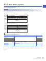
1.1
Processing of Each Function . . . . . . . . . . . . . . . . . . . . . . . . . . . . . . . . . . . . . . . . . . . . . . . . . . . . . . . . . . . . . . 15
1.2
Range Switching Function . . . . . . . . . . . . . . . . . . . . . . . . . . . . . . . . . . . . . . . . . . . . . . . . . . . . . . . . . . . . . . . . 16
1.3
A/D Conversion Enable/Disable Setting Function . . . . . . . . . . . . . . . . . . . . . . . . . . . . . . . . . . . . . . . . . . . . . 17
1.4
A/D Conversion Method . . . . . . . . . . . . . . . . . . . . . . . . . . . . . . . . . . . . . . . . . . . . . . . . . . . . . . . . . . . . . . . . . . 18
1.5
Scaling Function . . . . . . . . . . . . . . . . . . . . . . . . . . . . . . . . . . . . . . . . . . . . . . . . . . . . . . . . . . . . . . . . . . . . . . . . 22
1.6
Alert Output Function . . . . . . . . . . . . . . . . . . . . . . . . . . . . . . . . . . . . . . . . . . . . . . . . . . . . . . . . . . . . . . . . . . . . 26
CONTENTS
TERMS . . . . . . . . . . . . . . . . . . . . . . . . . . . . . . . . . . . . . . . . . . . . . . . . . . . . . . . . . . . . . . . . . . . . . . . . . . . . . . . . .13
Process alarm . . . . . . . . . . . . . . . . . . . . . . . . . . . . . . . . . . . . . . . . . . . . . . . . . . . . . . . . . . . . . . . . . . . . . . . . . . . 26
Rate alarm . . . . . . . . . . . . . . . . . . . . . . . . . . . . . . . . . . . . . . . . . . . . . . . . . . . . . . . . . . . . . . . . . . . . . . . . . . . . . . 29
1.7
Input Signal Error Detection Function. . . . . . . . . . . . . . . . . . . . . . . . . . . . . . . . . . . . . . . . . . . . . . . . . . . . . . . 33
When the function is used in the Q compatible mode . . . . . . . . . . . . . . . . . . . . . . . . . . . . . . . . . . . . . . . . . . . . . 41
1.8
Shift Function . . . . . . . . . . . . . . . . . . . . . . . . . . . . . . . . . . . . . . . . . . . . . . . . . . . . . . . . . . . . . . . . . . . . . . . . . . 46
1.9
Digital Clipping Function . . . . . . . . . . . . . . . . . . . . . . . . . . . . . . . . . . . . . . . . . . . . . . . . . . . . . . . . . . . . . . . . . 49
1.10
Difference Conversion Function . . . . . . . . . . . . . . . . . . . . . . . . . . . . . . . . . . . . . . . . . . . . . . . . . . . . . . . . . . . 51
1.11
Maximum Value/Minimum Value Hold Function . . . . . . . . . . . . . . . . . . . . . . . . . . . . . . . . . . . . . . . . . . . . . . . 55
1.12
Logging Function . . . . . . . . . . . . . . . . . . . . . . . . . . . . . . . . . . . . . . . . . . . . . . . . . . . . . . . . . . . . . . . . . . . . . . . 56
Stopping the logging operation . . . . . . . . . . . . . . . . . . . . . . . . . . . . . . . . . . . . . . . . . . . . . . . . . . . . . . . . . . . . . . 61
Logging hold request . . . . . . . . . . . . . . . . . . . . . . . . . . . . . . . . . . . . . . . . . . . . . . . . . . . . . . . . . . . . . . . . . . . . . . 64
Level trigger. . . . . . . . . . . . . . . . . . . . . . . . . . . . . . . . . . . . . . . . . . . . . . . . . . . . . . . . . . . . . . . . . . . . . . . . . . . . . 65
Initial settings of the logging function. . . . . . . . . . . . . . . . . . . . . . . . . . . . . . . . . . . . . . . . . . . . . . . . . . . . . . . . . . 68
Logging read function . . . . . . . . . . . . . . . . . . . . . . . . . . . . . . . . . . . . . . . . . . . . . . . . . . . . . . . . . . . . . . . . . . . . . 69
Saving to a CSV file. . . . . . . . . . . . . . . . . . . . . . . . . . . . . . . . . . . . . . . . . . . . . . . . . . . . . . . . . . . . . . . . . . . . . . . 74
Displaying logging data . . . . . . . . . . . . . . . . . . . . . . . . . . . . . . . . . . . . . . . . . . . . . . . . . . . . . . . . . . . . . . . . . . . . 75
1.13
Interrupt Function . . . . . . . . . . . . . . . . . . . . . . . . . . . . . . . . . . . . . . . . . . . . . . . . . . . . . . . . . . . . . . . . . . . . . . . 76
1.14
Error History Function . . . . . . . . . . . . . . . . . . . . . . . . . . . . . . . . . . . . . . . . . . . . . . . . . . . . . . . . . . . . . . . . . . . 79
1.15
Event History Function . . . . . . . . . . . . . . . . . . . . . . . . . . . . . . . . . . . . . . . . . . . . . . . . . . . . . . . . . . . . . . . . . . . 82
1.16
Backing up, Saving, and Restoring Offset/Gain Values . . . . . . . . . . . . . . . . . . . . . . . . . . . . . . . . . . . . . . . . 83
When the module-specific backup parameter is used. . . . . . . . . . . . . . . . . . . . . . . . . . . . . . . . . . . . . . . . . . . . . 83
When the module-specific backup parameter is not used. . . . . . . . . . . . . . . . . . . . . . . . . . . . . . . . . . . . . . . . . . 86
1.17
Q Compatible Mode Function. . . . . . . . . . . . . . . . . . . . . . . . . . . . . . . . . . . . . . . . . . . . . . . . . . . . . . . . . . . . . . 90
CHAPTER 2
PARAMETER SETTINGS
91
2.1
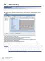
Basic Setting . . . . . . . . . . . . . . . . . . . . . . . . . . . . . . . . . . . . . . . . . . . . . . . . . . . . . . . . . . . . . . . . . . . . . . . . . . . 91
2.2
Application Setting . . . . . . . . . . . . . . . . . . . . . . . . . . . . . . . . . . . . . . . . . . . . . . . . . . . . . . . . . . . . . . . . . . . . . . 92
2.3
Interrupt Setting. . . . . . . . . . . . . . . . . . . . . . . . . . . . . . . . . . . . . . . . . . . . . . . . . . . . . . . . . . . . . . . . . . . . . . . . . 93
2.4
Refresh Setting . . . . . . . . . . . . . . . . . . . . . . . . . . . . . . . . . . . . . . . . . . . . . . . . . . . . . . . . . . . . . . . . . . . . . . . . . 94
Refresh processing time . . . . . . . . . . . . . . . . . . . . . . . . . . . . . . . . . . . . . . . . . . . . . . . . . . . . . . . . . . . . . . . . . . . 95
CHAPTER 3
TROUBLESHOOTING
96
3.1
Troubleshooting with the LEDs . . . . . . . . . . . . . . . . . . . . . . . . . . . . . . . . . . . . . . . . . . . . . . . . . . . . . . . . . . . . 96
3.2
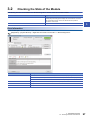
Checking the State of the Module . . . . . . . . . . . . . . . . . . . . . . . . . . . . . . . . . . . . . . . . . . . . . . . . . . . . . . . . . . 97
3.3
Troubleshooting by Symptom . . . . . . . . . . . . . . . . . . . . . . . . . . . . . . . . . . . . . . . . . . . . . . . . . . . . . . . . . . . . . 99
11
When the RUN LED flashes or turns off . . . . . . . . . . . . . . . . . . . . . . . . . . . . . . . . . . . . . . . . . . . . . . . . . . . . . . . 99
When the ERR LED turns on. . . . . . . . . . . . . . . . . . . . . . . . . . . . . . . . . . . . . . . . . . . . . . . . . . . . . . . . . . . . . . . . 99
When the ALM LED turns on or flashes . . . . . . . . . . . . . . . . . . . . . . . . . . . . . . . . . . . . . . . . . . . . . . . . . . . . . . 100
When a digital output value cannot be read . . . . . . . . . . . . . . . . . . . . . . . . . . . . . . . . . . . . . . . . . . . . . . . . . . . 101
When the digital output value does not fall within the range of accuracy . . . . . . . . . . . . . . . . . . . . . . . . . . . . . 102
3.4
List of Error Codes . . . . . . . . . . . . . . . . . . . . . . . . . . . . . . . . . . . . . . . . . . . . . . . . . . . . . . . . . . . . . . . . . . . . . 103
3.5
List of Alarm Codes. . . . . . . . . . . . . . . . . . . . . . . . . . . . . . . . . . . . . . . . . . . . . . . . . . . . . . . . . . . . . . . . . . . . . 106
APPENDICES
107
Appendix 1 Module Label . . . . . . . . . . . . . . . . . . . . . . . . . . . . . . . . . . . . . . . . . . . . . . . . . . . . . . . . . . . . . . . . . . . . . 107
Appendix 2 I/O Signals . . . . . . . . . . . . . . . . . . . . . . . . . . . . . . . . . . . . . . . . . . . . . . . . . . . . . . . . . . . . . . . . . . . . . . . 109
List of I/O signals . . . . . . . . . . . . . . . . . . . . . . . . . . . . . . . . . . . . . . . . . . . . . . . . . . . . . . . . . . . . . . . . . . . . . . . . 109
Details of input signals. . . . . . . . . . . . . . . . . . . . . . . . . . . . . . . . . . . . . . . . . . . . . . . . . . . . . . . . . . . . . . . . . . . . 110
Details of output signals . . . . . . . . . . . . . . . . . . . . . . . . . . . . . . . . . . . . . . . . . . . . . . . . . . . . . . . . . . . . . . . . . . 116
Appendix 3 Buffer Memory Areas. . . . . . . . . . . . . . . . . . . . . . . . . . . . . . . . . . . . . . . . . . . . . . . . . . . . . . . . . . . . . . . 118
List of buffer memory addresses . . . . . . . . . . . . . . . . . . . . . . . . . . . . . . . . . . . . . . . . . . . . . . . . . . . . . . . . . . . . 118
Details of buffer memory addresses . . . . . . . . . . . . . . . . . . . . . . . . . . . . . . . . . . . . . . . . . . . . . . . . . . . . . . . . . 138
Appendix 4 Dedicated Instructions . . . . . . . . . . . . . . . . . . . . . . . . . . . . . . . . . . . . . . . . . . . . . . . . . . . . . . . . . . . . . 197
Instruction list. . . . . . . . . . . . . . . . . . . . . . . . . . . . . . . . . . . . . . . . . . . . . . . . . . . . . . . . . . . . . . . . . . . . . . . . . . . 197
INDEX
198
REVISIONS . . . . . . . . . . . . . . . . . . . . . . . . . . . . . . . . . . . . . . . . . . . . . . . . . . . . . . . . . . . . . . . . . . . . . . . . . . . . .200
WARRANTY . . . . . . . . . . . . . . . . . . . . . . . . . . . . . . . . . . . . . . . . . . . . . . . . . . . . . . . . . . . . . . . . . . . . . . . . . . . .201
TRADEMARKS . . . . . . . . . . . . . . . . . . . . . . . . . . . . . . . . . . . . . . . . . . . . . . . . . . . . . . . . . . . . . . . . . . . . . . . . . .202
12
RELEVANT MANUALS
Manual name [manual number]
Description
Available form
MELSEC iQ-R Channel Isolated Analog-Digital Converter Module
User's Manual (Application)
[SH-081487ENG] (this manual)
Functions, parameter settings, troubleshooting, I/O signals,
and buffer memory of the A/D converter module
Print book
MELSEC iQ-R Channel Isolated Analog-Digital Converter Module
User's Manual (Startup)
[SH-081485ENG]
Performance specifications, procedures before operation,
wiring, programming, and offset/gain setting of the A/D
converter module
Print book
MELSEC iQ-R Programming Manual (Instructions, Standard
Functions/Function Blocks)
[SH-081266ENG]
Instructions for the CPU module, dedicated instructions for
the intelligent function modules, and standard functions/
function blocks
e-Manual
EPUB
PDF
e-Manual
EPUB
PDF
e-Manual
EPUB
PDF
e-Manual refers to the Mitsubishi FA electronic book manuals that can be browsed using a dedicated tool.
e-Manual has the following features:
• Required information can be cross-searched in multiple manuals.
• Other manuals can be accessed from the links in the manual.
• The hardware specifications of each part can be found from the product figures.
• Pages that users often browse can be bookmarked.
TERMS
Unless otherwise specified, this manual uses the following terms.
Term
Description
A/D converter module
The abbreviation for the MELSEC iQ-R series channel isolated analog-digital converter module
GX Works3
The product name of the software package for the MELSEC programmable controllers
Q compatible mode
A mode in which the module operates with the buffer memory map converted to the equivalent one of the MELSEC Q series
R mode
A mode in which the module operates with the buffer memory map that has been newly laid out in the MELSEC iQ-R series
Watchdog timer error
An error that occurs if the internal processing of the A/D converter module fails. The module monitors its own internal
processing by using the watchdog timer.
Engineering tool
Another term for GX Works3
Offset/gain setting mode
A mode used for performing the offset/gain setting
Global label
A label that is valid for all the program data when multiple program data are created in the project. There are two types of
global label: a module specific label (module label), which is generated automatically by GX Works3, and an optional label,
which can be created for any specified device.
Factory default setting
A generic term for analog input ranges of 0 to 10V, 0 to 5V, 1 to 5V, -10 to 10V, 0 to 20mA, 4 to 20mA, 1 to 5V (extended
mode), and 4 to 20mA (extended mode).
In the window on the engineering tool, 4 to 20mA (extended mode) and 1 to 5V (extended mode) are displayed as the
following:
• 4 to 20mA (Extension)
• 1 to 5V (Extension)
Normal mode
A mode used for normal A/D conversion. In the engineering tool, the item name of the mode is displayed as "Normal mode
(A/D conversion process)".
Buffer memory
A memory in an intelligent module for storing data (such as setting values and monitored values) to be transferred to the
CPU module
User range
An analog input range where any value can be set. This range can be set in the offset/gain setting.
Module Label
A label that represents one of memory areas (I/O signals and buffer memory areas) specific to each module in a given
character string. For the module used, GX Works3 automatically generates this label, which can be used as a global label.
13
1
FUNCTIONS
This chapter describes the functions of the A/D converter module and the setting procedures for those functions.
For details on the I/O signals and the buffer memory, refer to the following.
Page 109 I/O Signals
Page 118 Buffer Memory Areas
This chapter describes buffer memory addresses for CH1.
For details on the buffer memory addresses after CH2, refer to the following.
Page 118 List of buffer memory addresses
14
1 FUNCTIONS
1.1
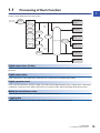
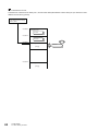
Processing of Each Function
1
The functions are processed in the order shown below. If multiple functions are enabled, the output of the first processed
function is used as the input of the next function.
Analog input
(CH1 to CH16)
Input signal
error detection
function
CH Digital
output value
(32 bits)
A/D conversion
method
Sampling
processing
Rate
alarm
CH Digital
output value
Count average
Digital clipping
function
Time average
Alert output
function
Moving average
CH Maximum
value
Scaling function
Logging function
Primary delay
filter
Maximum value/
minimum value
hold function
CH Minimum
value
Shift function
Process
alarm
Difference
conversion
function
CH Digital
operation value
CH Logging
data
Digital output value (32 bits)
These values are the digital values after the sampling processing, each averaging processing, or primary delay filter has been
performed.
Digital output value
These values are the 16-bit digital output values that were converted from 32-bit digital output values.
Digital operation value
These values are obtained by operating a digital output value using the digital clipping function, scaling function, shift function,
or difference conversion function. When each function is not used, the same value as the digital output value is stored.
Maximum and minimum value
The maximum and minimum values of the digital operation values are stored.
Logging data
When the logging function is used, digital output values or digital operation values are collected.
1 FUNCTIONS
1.1 Processing of Each Function
15
1.2
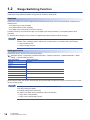
Range Switching Function
This function allows switching the input range of an analog input for each channel.
Switching the range makes it possible to change the I/O conversion characteristic.
Operation
Analog input values are converted to digital values within the set input range, and the converted values are stored in the
following areas.
• 'CH1 Digital output value' (Un\G400)
• 'CH1 Digital operation value' (Un\G402)
• 'CH1 Digital output value (32 bits)' (Un\G410, Un\G411)
The data of 32768 or more cannot be output to 'CH1 Digital output value' (Un\G400) or 'CH1 Digital operation value'
(Un\G402).
To check the data of 32768 or more, monitor 'CH1 Digital output value (32 bits)' (Un\G410, Un\G411).
Digital output values (32768 to 36767) in the extended mode can be monitored within the range of 'CH1 Digital
operation value' (Un\G402) with the shift function or scaling function. For details, refer to the following.
Page 46 Shift Function
Page 22 Scaling Function
Setting procedure
Set the input range to be used in the "Input range setting".
Navigation window [Parameter] [Module Information] Module model name [Module Parameter] "Basic
setting" "Range switching function"
Input range setting
Digital output value
4 to 20mA
0 to 32000
0 to 20mA
1 to 5V
0 to 5V
-10 to 10V
-32000 to 32000
0 to 10V
0 to 32000
4 to 20mA (extended mode)
-8000 to 36000
1 to 5V (extended mode)
User range setting
-32000 to 32000
After the data is written, the range is switched when the programmable controller power supply is turned off and on or when
the CPU module is reset.
The range can be switched or set with the following buffer memory areas.
'CH1 Range setting' (Un\G598)
'CH1 Range setting monitor' (Un\G430)
For details on the buffer memory addresses, refer to the following.
Page 188 CH1 Range setting
Page 151 CH1 Range setting monitor
16
1 FUNCTIONS
1.2 Range Switching Function
1.3
A/D Conversion Enable/Disable Setting Function
1
This function controls whether to enable or disable the A/D conversion for each channel.
Disabling the A/D conversion for unused channels reduces the A/D conversion cycles.
Setting procedure
Set "A/D conversion enable/disable setting" to "A/D conversion enable" or "A/D conversion disable".
Navigation window [Parameter] [Module Information] Module model name [Module Parameter] "Basic
setting" "A/D conversion enable/disable setting function"
1 FUNCTIONS
1.3 A/D Conversion Enable/Disable Setting Function
17
1.4
A/D Conversion Method
An A/D conversion method can be set for each channel.
Sampling processing
This function converts analog input values to digital values at every sampling period and stores the digital output values in
buffer memory areas.
The sampling period is "Conversion speed (10ms) number of conversion enabled channels".
Whether to enable or disable the A/D conversion can be set for each channel. Disabling the A/D conversion
for unused channels reduces the A/D conversion cycles.
Conversion cycle that applies when CH1 to CH3 get A/D conversion enabled
• 10 3 = 30 (ms)
The conversion cycle is 30 (ms).
Digital output values and digital operation values of CH1 to CH3 are updated every 30ms.
Averaging processing
The A/D converter module performs the averaging processing on digital output values for each channel. The processed
values are stored in the buffer memory area.
The following three types of averaging processing are provided.
• Time average
• Count average
• Moving average
■Time average
The A/D converter module executes the A/D conversion for the setting time, and performs the averaging processing on the
total value excluding the maximum and the minimum values. The processed values are stored in the buffer memory area.
Setting time
Set a value that satisfies the following condition.
Lower limit value to be set ≥ Conversion speed × Number of conversion enabled channels × Minimum number of processing times (4 times)
Ex.
The following shows the lower limit value to be set for when CH1 to CH8 are used.
10 (ms) 8 (CH) 4 (times) = 320 (ms)
• Processing times
The number of processing times within the set time changes depending on the number of channels where the A/D conversion
is enabled.
Number of processing times =
Setting time
(Number of conversion enabled channels × Conversion speed)
Ex.
The following table shows the processing times with the setting below.
Item
Setting
Number of channels where the A/D conversion is enabled
Four channels (CH1 to CH4)
Setting time
250ms
250
(4 × 10)
*1
= 6.25*1
Values after the decimal point are omitted.
Conversion is processed 6 times and the mean value is output.
18
1 FUNCTIONS
1.4 A/D Conversion Method
When the number of processing times is less than 4 due to the set time, a time average setting range error
1
(error code: 192H) occurs. The value 0 is stored in the following buffer memory areas.
• 'CH1 Digital output value' (Un\G400)
• 'CH1 Digital operation value' (Un\G402)
• 'CH1 Digital output value (32 bits)' (Un\G410, Un\G411)
■Count average
The A/D converter module executes the A/D conversion for a set number of times, and performs the averaging processing on
the total value excluding the maximum and the minimum values. The processed values are stored in the buffer memory area.
The time taken for the mean value calculated through the average processing to be stored in the buffer memory changes
depending on the number of channels where the A/D conversion is enabled.
Processing time = Set number of times (Number of conversion enabled channels Conversion speed)
Ex.
The following table shows the processing time with the setting below.
Item
Setting
Number of channels where the A/D conversion is enabled
Four channels (CH1 to CH4)
Set number of times
Five times
5 (times) (4 (CH) 10 (ms)) = 200 (ms)
A mean value is output every 200ms.
Because the count average requires a sum of at least two counts excluding the maximum and minimum
values, the set number of times should be four or more.
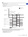
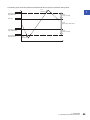
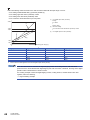
■Moving average
The A/D converter module averages digital output values taken at every sampling period for a specified number of times, and
stores the mean value in the buffer memory area. Since the averaging processing is performed on a moving set of sampling,
the latest digital output values can be obtained.
The following figure shows the moving average processing of when the set number of times is five.
Digital output value
32000
Sampling cycle
(3)
(2)
(4)
(5)
(1)
(6)
(7)
(8)
(9)
(12)
(10) (11)
16000
1st storage (a)
2nd storage (b)
3rd storage (c)
0
Time [ms]
'CH1 Digital output value'
(Un\G400)
0
(a)
(b)
(c)
ON
'A/D conversion
completed flag' (XE)
OFF
Data transition in buffer memory
1st storage (a)
2nd storage (b)
3rd storage (c)
(1) + (2) + (3) + (4)+ (5)
(2) + (3) + (4) + (5)+ (6)
(3) + (4) + (5) + (6)+ (7)
5
5
5
1 FUNCTIONS
1.4 A/D Conversion Method
19
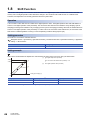
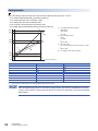
Primary delay filter
Depending on the set time constant, transient noise of analog input is smoothed. The smoothed digital output values are
stored in the buffer memory area.
Time constant is the time taken for the digital output value to reach 63.2% of the steady-state value.
The following shows the relational expressions of time constants and digital output values.
When n = 1*1
Yn = 0
When n = 2
Yn = Xn-1 +
Δt
(Xn - Xn-1)
Δt + TA
When n 3
Yn = Yn-1 +
Yn
Yn-1
n
Xn
Xn-1
T
TA
*1
Δt
(Xn - Yn-1)
Δt + TA
: Present digital output value
: Last digital output value
: Number of sampling
: Digital output value before smoothing
: Last digital output value before smoothing
: Conversion time
: Time constant
The corresponding bit of 'A/D conversion completed flag' (Un\G42) turns on when n 2.
Ex.
Digital output value when an analog input value is changed from 0 to 1V
The following figure shows the change of the digital output value with the input range of 0 to 10V and time constant
(Conversion cycle Primary delay filter) of 40ms.
After 40ms from the analog input value becomes 1V, the digital output value reaches 63.2% of the digital output value of when
the sampling processing is selected.
Analog input value
Digital output value
1.2
3840
1.0
3200
2560
0.8
63.2%
Analog input value (V) 0.6
1920 Digital output value
0.4
1280
0.2
640
0
0
0
40
Elapsed time (ms)
20
1 FUNCTIONS
1.4 A/D Conversion Method
Setting procedure
1
■Sampling processing
Set "Averaging process specification" to "Sampling processing".
Navigation window [Parameter] [Module Information] Module name [Module Parameter] "Basic setting"
"A/D conversion method"
■Averaging processing and primary delay filter
1.
Set "Averaging process specification" to "Time average", "Count average", "Moving average", or "Primary delay filter".
Navigation window [Parameter] [Module Information] Module model name [Module Parameter] "Basic
setting" "A/D conversion method"
2.
Set a value for "Time average/Count average/Moving average/Primary delay filter constant setting".
Item
Setting range
Time average
40 to 5000 (ms)*1
Count average
4 to 500 (times)
Moving average
2 to 200 (times)
Primary delay filter
1 to 500 (times)
*1
Set a value greater than the value calculated by the following formula as the time average.
Conversion speed Number of conversion enabled channels Minimum processing times (4 times)
1 FUNCTIONS
1.4 A/D Conversion Method
21
1.5
Scaling Function
This function performs the scale conversion on digital output values. The values are converted within a specified range
between a scaling upper limit value and scaling lower limit value. This function helps reduce the time taken for creating a scale
conversion program.
The converted values are stored in 'CH1 Digital operation value' (Un\G402).
Concept of scaling setting
Ex.
When the input range is set to -10 to 10V:
For the scaling lower limit value, set a value corresponding to the lower limit value of the input range (-32000).
For the scaling upper limit value, set a value corresponding to the upper limit value of the input range (32000).
Calculating the scaling value
The scale conversion is based on the following formula. (In scale conversion, values are rounded to the nearest whole
number.)
Current: 0 to 20mA, 4 to 20mA, 4 to 20mA (extended mode)*1, user range setting (current)
Voltage: 0 to 10V, 0 to 5V, 1 to 5V, 1 to 5V (extended mode)*1, user range setting (voltage)
DX × (SH - SL)
+ SL
DMax
DY =
Voltage: -10 to 10V
DX × (SH - SL)
(SH + SL)
+
DMax - DMin
2
DY =
DX
DY
DMax
DMin
SH
SL
*1
: Digital output value
: Scaling value (Digital operation value)
: Maximum digital output value of the input range in use
: Minimum digital output value of the input range in use
: Scaling upper limit value
: Scaling lower limit value
Although the range of the digital output value in the extended mode is -8000 to 36000, this function performs the scale conversion for
digital output values within the range of 0 to 32000.
When the calculated digital operation value exceeds 32767, the value 32767 is stored as the digital operation
value. When the calculated digital operation value is falls below -32768, the value -32768 is stored.
Setting procedure
1.
Set "Scaling enable/disable setting" to "Enable".
Navigation window [Parameter] [Module Information] Module model name [Module Parameter] "Application
setting" "Scaling setting"
2.
Set values for "Scaling upper limit value" and "Scaling lower limit value".
Item
Setting range
Scaling upper limit value
-32000 to 32000
Scaling lower limit value
• Even when the scaling upper limit value and the scaling lower limit value are set so that the change is
greater than the resolution, the resolution will not increase.
• If the relation between the values is the scaling lower limit value > the scaling upper limit value, the scale
conversion can be performed according to a negative slope.
• Set the scaling with the condition "Scaling upper limit value Scaling lower limit value".
22
1 FUNCTIONS
1.5 Scaling Function
Setting example
1
Ex.
When 20000 is set to the scaling upper limit value and 4000 is set to the scaling lower limit value for the module with the input
range of 0 to 5V
Scaling upper limit value 20000
Scaling lower limit value 4000
32000
Analog input voltage (V)
0
0
5
Voltage input (V)
Digital output value*1
Digital operation value
(scaling value)
0
0
4000
1
6400
7200
2
12800
10400
3
19200
13600
4
25600
16800
5
32000
20000
*1
These values are also applied to the case of digital output values (32 bits).
Ex.
When 20000 is set to the scaling upper limit value and 4000 is set to the scaling lower limit value for the module with the input
range of -10 to 10V
Scaling upper limit value: 20000
32000
0
Scaling lower limit value: 4000
-32000
-10
Analog input voltage (V)
0
10
Voltage input (V)
Digital output value*1
Digital operation value
(scaling value)
-10
-32000
4000
-5
-16000
8000
0
0
12000
5
16000
16000
10
32000
20000
*1
These values are also applied to the case of digital output values (32 bits).
1 FUNCTIONS
1.5 Scaling Function
23
Ex.
When 20000 is set to the scaling upper limit value and 4000 is set to the scaling lower limit value for the module with the input
range of 1 to 5V (extended mode)
Scaling upper limit value: 20000
Scaling lower limit value: 4000
36000
32000
0
-8000
1
5 5.5
Analog input voltage (V)
Voltage input (V)
Digital output value
16 bits
32 bits
Digital operation value
(scaling value)
0
-8000
-8000
0
1
0
0
4000
2
8000
8000
8000
3
16000
16000
12000
4
24000
24000
16000
5
32000
32000
20000
5.5
32767*1
36000
22000
*1
24
0
Because the value exceeds the range of -32768 to 32767, the value is fixed to 32767 (the upper limit value).
1 FUNCTIONS
1.5 Scaling Function
Ex.
When 32000 is set to the scaling upper limit value and -32000 is set to the scaling lower limit value for the module with the
1
input range of 4 to 20mA (extended mode)
Scaling upper limit value: 32000
Scaling lower limit value: -32000
36000
32000
0
-8000
0
4
20 22
Analog input current (mA)
Current input (mA)
Digital output value
16 bits
32 bits
Digital operation value
(scaling value)
0
-8000
-8000
-32768*1
4
0
0
-32000
8
8000
8000
-16000
12
16000
16000
0
16
24000
24000
16000
20
32000
32000
32000
20.24
32480
32480
32767*2
22
32767*2
36000
32767*2
*1
*2
Because the value falls below the range of -32768 to 32767, the value is fixed to -32768 (the lower limit value).
Because the value exceeds the range of -32768 to 32767, the value is fixed to 32767 (the upper limit value).
When the scaling function is used with the digital clipping function, the scale conversion is performed on the
digital operation values after digital clipping.
1 FUNCTIONS
1.5 Scaling Function
25
1.6
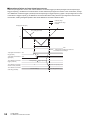
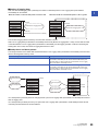
Alert Output Function
This section describes process alarms and rate alarms used for the alert output function.
Process alarm
This function outputs an alert when a digital operation value enters the preset alert output range.
Digital operation value
Alert output range
Out of alert output range
Included
Alert
Alert
Upper upper limit value
Upper lower limit value
Alert cleared
Alert cleared
'CH1 Digital operation
value' (Un\G402)
Alert cleared
Lower upper limit value
'CH2 Digital operation
value' (Un\G602)
Lower lower limit value
Alert
Time
ON
'CH1 Alert output flag
(Process alarm upper limit)'
(Un\G36, b0)
OFF
ON
'CH1 Alert output flag
(Process alarm lower limit)'
(Un\G37, b0)
OFF
ON
'CH2 Alert output flag
(Process alarm upper limit)'
(Un\G36, b1)
OFF
ON
'Alert output signal' (X8)
26
1 FUNCTIONS
1.6 Alert Output Function
OFF
Operation
1
■Operation performed when an alert is output
When a digital operation value is equal to or greater than 'CH1 Process alarm upper upper limit value' (Un\G514), or the value
is equal to or smaller than 'CH1 Process alarm lower lower limit value' (Un\G520) and the value enters the alarm output range,
an alert is output as follows.
• Alarm ON (1) is stored in 'Alert output flag (Process alarm upper limit)' (Un\G36) or 'Alert output flag (Process alarm lower
limit)' (Un\G37).
• 'Alert output signal' (X8) turns on.
• The ALM LED turns on.
In addition, an alarm code is stored in 'Latest alarm code' (Un\G2).
For details on the alarm codes, refer to the following.
Page 106 List of Alarm Codes
The A/D conversion on a channel where an alert was output continues.
■Operation after an alert was output
After an alert was output, if the digital operation value does not satisfy the alert output condition due to being smaller than
'CH1 Process alarm upper lower limit value' (Un\G516) or being greater than 'CH1 Process alarm lower upper limit value'
(Un\G518), Normal (0) is stored in a bit position corresponding to the channel number of 'Alert output flag (Process alarm
upper limit)' (Un\G36) or 'Alert output flag (Process alarm lower limit)' (Un\G37).
In addition, when all the bits of 'Alert output flag (Process alarm upper limit)' (Un\G36) and 'Alert output flag (Process alarm
lower limit)' (Un\G37) return to Normal (0), 'Alert output signal' (X8) turns off and the ALM LED turns off. However, the alarm
code stored in 'Latest alarm code' (Un\G2) is not cleared. To clear the alarm code, turn on and off 'Error clear request (YF)'
after all the bits of 'Alert output flag (Process alarm upper limit)' (Un\G36) and 'Alert output flag (Process alarm lower limit)'
(Un\G37) return to Normal (0).
Detection cycle
When time average is specified, the function works at every interval of the time (for averaging). When count average is
specified, the function works at every count (for averaging).
When the sampling processing, moving average, and primary delay filter is specified, this function works at every sampling
cycle.
Detection target for outputting an alert
When the digital clipping function, scaling function, shift function, or difference conversion function is used, the digital
operation value to which digital clipping, scale conversion, shift-and-add, or difference conversion is performed is the
detection target for outputting an alert. Set values for 'CH1 Process alarm upper upper limit value' (Un\G514), 'CH1 Process
alarm upper lower limit value' (Un\G516), 'CH1 Process alarm lower upper limit value' (Un\G518), and 'CH1 Process alarm
lower lower limit value' (Un\G520) while considering the digital clipping, scale conversion, shift-and-add, and difference
conversion.
1 FUNCTIONS
1.6 Alert Output Function
27
Setting procedure
1.
Set "Alert output setting (Process alarm)" to "Enable".
Navigation window [Parameter] [Module Information] Module model name [Module Parameter] "Application
setting" "Alert output function (Process alarm)"
2.
Set values for "Process alarm upper upper limit value", "Process alarm upper lower limit value", "Process alarm lower
upper limit value", and "Process alarm lower lower limit value".
Item
Setting range
Process alarm upper upper limit value
-32768 to 32767
Process alarm upper lower limit value
Process alarm lower upper limit value
Process alarm lower lower limit value
Set values within the range satisfying the condition "Process alarm upper upper limit value Process alarm
upper lower limit value Process alarm lower upper limit value Process alarm lower lower limit value". If a
value out of the range is set, a process alarm upper lower limit value setting range error (error code: 1BH)
occurs.
28
1 FUNCTIONS
1.6 Alert Output Function
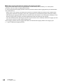
Rate alarm
1
This function outputs an alert when the change rate of a digital output value is equal to or greater than the rate alarm upper
limit value, or the rate is equal to or smaller than the rate alarm lower limit value.
Digital output value
'CH1 Digital output value' (Un\G400)
Rate alarm alert
detection cycle
'CH2 Digital output value' (Un\G600)
(1)
(2)
Time
(3)
The change amount of the digital output value is converted to the change
rate at every rate alarm alert detection cycle. "Change rate > 0" if the change
amount increases, and "Change rate < 0" if the change amount decreases.
Change rate of CH1 Digital output value
Change rate of the
digital output value (%)
Ex.
For the rate alarm upper limit value: 5.0%, and
the rate alarm lower limit value: -5.0%
Rate alarm upper
limit value
(CH1: Un\G524,
CH2: Un\G724)
(1)
(2)
No.
(3)
0
Change rate of the digital output value
CH1
Rate alarm lower
limit value
(CH1: Un\G526,
CH2: Un\G726)
(1)
10.0%
(2)
3.0%
(3)
10.0%
:
:
:
:
Change rate of CH2 Digital output value
Time
ON
'CH1 Alert output flag
(Rate alarm upper
limit)' (Un\G38, b0)
OFF
CH2
An upper limit
alert issued
for CH1
No alert
issued
An upper limit
alert issued
for CH1
-3.0%
No alert
issued
-10.0% A lower limit
alert issued
for CH2
-3.0%
No alert
issued
:
:
ON
OFF
OFF
ON
'CH2 Alert output flag
(Rate alarm lower
limit)' (Un\G39, b1)
OFF
OFF
ON
'Alert output signal'
(X8)
OFF
OFF
Controlled by the A/D converter module
1 FUNCTIONS
1.6 Alert Output Function
29
Operation
■Operation performed when an alert is output
Digital output values are monitored on the rate alarm alert detection cycle. When a change rate of a digital output value (from
a previous value) is equal to or more than the rate alarm upper limit value, or the rate is equal to or less than the rate alarm
lower limit value, an alert is output as follows.
• Alarm ON (1) is stored in 'Alert output flag (Rate alarm upper limit)' (Un\G38) or 'Alert output flag (Rate alarm lower limit)'
(Un\G39).
• 'Alert output signal' (X8) turns on.
• The ALM LED turns on.
In addition, an alarm code is stored in 'Latest alarm code' (Un\G2).
For details on the alarm codes, refer to the following.
Page 106 List of Alarm Codes
The A/D conversion on a channel where an alert was output continues.
■Operation after an alert was output
After an alert was output, if the change rate of a digital output value does not satisfy the alert output conditions due to being
smaller than the rate alarm upper limit value or being greater than the rate alarm lower limit value, Normal (0) is stored in a bit
position corresponding to the channel number of 'Alert output flag (Rate alarm upper limit)' (Un\G38) or 'Alert output flag (Rate
alarm lower limit)' (Un\G39).
In addition, when all 'Alert output flag (Rate alarm upper limit)' (Un\G38) and 'Alert output flag (Rate alarm lower limit)'
(Un\G39) return to Normal (0), 'Alert output signal' (X8) turns off and the ALM LED turns off. However, the alarm code stored
in 'Latest alarm code' (Un\G2) is not cleared. To clear the alarm code, turn on and off 'Error clear request (YF)' after all the bits
of 'Alert output flag (Rate alarm upper limit)' (Un\G38) and 'Alert output flag (Rate alarm lower limit)' (Un\G39) return to Normal
(0).
Detection cycle
Set the rate alarm alert detection cycle in 'CH1 Rate alarm alert detection cycle setting' (Un\G522).
The rate alarm alert detection cycle is the value calculated by multiplying the set value by the conversion cycle.
Ex.
The rate alarm alert detection cycle under the following conditions
• A/D conversion-enabled channels: CH1 to CH3
• 'CH1 Rate alarm alert detection cycle setting' (Un\G522): 5 (times)
The rate alarm alert detection cycle is 150ms. (10ms 3 (CH) 5 (times))
Digital output values are compared in 150ms intervals to check the change rate.
30
1 FUNCTIONS
1.6 Alert Output Function
Judgment of rate alarm
1
A change rate is judged with 'CH1 Rate alarm upper limit value' (Un\G524) and 'CH1 Rate alarm lower limit value' (Un\G526)
converted to digital values per rate alarm alert detection cycle.
The following shows the conversion formula of judgment values used for the rate alarm detection.
RH or RL
Value used for judgement at each Rate alarm alert detection cycle [digit] =
1000
× DMax
Item
Description
RH
Rate alarm upper limit value (Unit: 0.1%)
RL
Rate alarm lower limit value (Unit: 0.1%)
DMax
Maximum digital output value of the input range
Other than extended mode: 32000
Extended mode: 36000
Values after the decimal point are omitted.
Ex.
The judgment value under the following conditions
• Input range: 4 to 20mA
• A/D conversion-enabled channel: CH1
• 'CH1 Averaging process specification' (Un\G501): Sampling processing (0)
• 'CH1 Rate alarm alert detection cycle setting' (Un\G522): 5 (times)
• 'CH1 Rate alarm upper limit value' (Un\G524): 250 (25.0%)
• 'CH1 Rate alarm lower limit value' (Un\G526): 50 (5.0%)
Upper limit value:
250
× 32000 = 8000 (digit)
1000
Lower limit value:
50
× 32000 = 1600 (digit)
1000
The present value is compared to the previous value (50ms) in a rate alarm alert detection cycle of 50ms (sampling period
10ms 5). A digital value is judged if it increases 8000 digits (25.0%) or more, or if the increase is 1600 digits (5.0%) or less
from the previous value (when the maximum digital output value is 32000).
Use the following formula to calculate a change rate to be set based on the change amount of voltage and current to detect an
alert.
*1
Change amount of the voltage (current) to detect an alert (V(mA))
Change rate to be set (0.1%) =
*1
Gain voltage (current) (V(mA)) - Offset voltage (current) (V(mA))
× 1000
Values after the decimal point are omitted.
Application examples of rate alarms
A rate alarm serves to monitor that the variation rate of a digital output value lies in a limited range as shown below:
Ex.
To monitor that a rising rate of a digital output value is within the specified range
Change rate of the digital output value (%)
Rate alarm upper value
+30%
+20%
Rate alarm lower value
0
Time
1 FUNCTIONS
1.6 Alert Output Function
31
Ex.
To monitor that a drop rate of a digital output value is within the specified range
Change rate of the digital output value (%)
0
Rate alarm upper value
Time
-20%
-30%
Rate alarm lower value
Ex.
To monitor that a change rate of a digital output value is within the specified range
Change rate of the digital output value (%)
Rate alarm upper value
+10%
0
Time
-10%
Rate alarm lower value
Setting procedure
1.
Set "Alert output setting (Rate alarm)" to "Enable".
Navigation window [Parameter] [Module Information] Module model name [Module Parameter] "Application
setting" "Alert output function (Rate alarm)"
2.
Set an alert detection cycle of rate alarms.
Set the cycle in "Rate alarm alert detection cycle setting".
Item
Setting range
Rate alarm alert detection cycle setting
1 to 32000 (times)
In the channel where a value out of the range is set, a rate alarm alert detection cycle setting range error
(error code: 1B9H) occurs.
3.
Set values for "Rate alarm upper limit value" and "Rate alarm lower limit value".
Set a value for the maximum value of the digital output value in increments of 0.1%.
• Other than extended mode of the input range: 32000
• Extended mode of the input range: 36000
Item
Setting range
Rate alarm upper limit value
-3276.8 to 3276.7 (%)
Rate alarm lower limit value
Set values within the range satisfying the condition "Rate alarm upper limit value > Rate alarm lower limit
value".
If a value out of the range is set, a rate alarm upper/lower limit setting value inversion error (error code:
1BAH) occurs.
32
1 FUNCTIONS
1.6 Alert Output Function
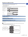
1.7
Input Signal Error Detection Function
1
This function outputs an alarm when an analog input value exceeds the preset range.
Detection range
Out of detection range
Analog input value
Included
Input signal error detection
upper limit value
CH2 Analog
input value
CH1 Analog
input value
Input signal error detection
lower limit value
Normal
input value
Error
detection
Error
detection
Time
ON
'CH1 Input signal error detection flag'
(Un\G40, b0)
OFF
OFF
ON
'CH2 Input signal error detection flag'
(Un\G40, b1)
OFF
'Input signal error detection signal'
(XC)
OFF
OFF
ON
OFF
ON
'Error clear request' (YF)
OFF
Controlled by the A/D converter module
Controlled by the program
Errors can be cleared using the input signal error detection auto-clear enable/disable setting. For details, refer
to the following.
Page 36 Clearing input signal errors
1 FUNCTIONS
1.7 Input Signal Error Detection Function
33
Detection method
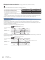
One of the following detection methods can be selected.
Detection method
Detection condition
0: Disable
Input signal errors are not detected.
1: Upper and lower limit
detection
An input signal error is detected when the
analog input value is equal to or greater
than the input signal error detection upper
limit value, or when the analog input value
is equal to or smaller than the input signal
error detection lower limit value.
Analog input value
Error
detection
Input signal error
detection upper limit value
Input signal error
detection lower limit value
Error
detection
Time
2: Lower limit detection
An input signal error is detected when the
analog input value is equal to or smaller
than the input signal error detection lower
limit value.
Analog input value
No error
detection
Input signal error
detection upper limit value
Input signal error
detection lower limit value
Error
detection
Time
3: Upper limit detection
An input signal error is detected when the
analog input value is equal to or greater
than the input signal error detection upper
limit value.
Analog input value
Error
detection
Input signal error
detection upper limit value
Input signal error
detection lower limit value
No error
detection
Time
4: Simple disconnection
detection
34
Simple disconnection detection is performed. For details, refer to the following.
Page 35 Simple disconnection detection
1 FUNCTIONS
1.7 Input Signal Error Detection Function
■Simple disconnection detection
This function outputs an alarm when an analog input value is 0.5V or smaller or 2mA or smaller.
1
By combining this function with the extended mode in the input range setting, simple disconnection detection is enabled.
When an analog input value satisfies either of the following conditions, a disconnection occurs and 'Input signal error
detection flag' (Un\G40) turns on.
Input range
Disconnection detection value
4 to 20mA (extended mode)
Analog input value 2mA
1 to 5V (extended mode)
Analog input value 0.5V
Analog input value
2mA or 0.5V
Error
detection
Time
The settings for 'CH1 Input signal error detection lower limit set value' (Un\G529) and 'CH1 Input signal error detection upper
limit set value' (Un\G530) are ignored.
Notification
When an input signal error is detected, an error is notified as follows.
• Input signal error (1) is stored in the corresponding bit of 'Input signal error detection flag' (Un\G40).
• 'Input signal error detection signal' (XC) turns on.
• The ALM LED flashes.
In addition, an alarm code is stored in 'Latest alarm code' (Un\G2). Alarm codes are stored whenever the analog input
satisfies the condition for the input signal error detection.
For details on the alarm codes, refer to the following.
Page 106 List of Alarm Codes
Operation
On the channel where an error is detected, the last digital output value and digital operation value just before the error was
detected are stored.
When the analog input does not satisfy the condition of the input signal error detection, the A/D conversion resumes
regardless of the reset on 'Input signal error detection flag' (Un\G40) and 'Input signal error detection signal' (XC). (The ALM
LED remains flashing.)
• When an input signal error occurs, the digital output value and digital operation value are not updated.
• The A/D conversion continues on the channel where no Input signal error is detected.
• Whether an input signal error occurred is judged with the value when the first A/D conversion is completed.
Thus, the corresponding bit of 'A/D conversion completed flag' (Un\G42) turns on even when an input signal
error is detected.
Detection cycle
This function works at every sampling cycle.
1 FUNCTIONS
1.7 Input Signal Error Detection Function
35
Clearing input signal errors
One of the following methods for clearing input signal errors can be selected by setting 'Input signal error detection auto-clear
enable/disable setting' (Un\G302).
■When Input signal error detection auto-clear enable/disable setting is set to Enable (0)
After the analog input value returns within the setting range, the A/D converter module arranges the following status
automatically. After the analog input value returns within the setting range, turning on and off 'Error clear request' (YF) is not
required.
• 'Input signal error detection flag' (Un\G40) is cleared.
• 'Input signal error detection signal' (XC) turns off.
• The ALM LED turns off.
'Latest alarm code' (Un\G2) is not cleared.
After the analog input value returns within the setting range, turn on and off 'Error clear request' (YF) to clear
'Latest alarm code' (Un\G2).
36
1 FUNCTIONS
1.7 Input Signal Error Detection Function
Ex.
The following figure shows the operation when an analog input value falls below 2.4mA and returns within the normal range
1
under the following condition.
• 'Input signal error detection auto-clear enable/disable setting' (Un\G302): Enable (0)
• Input range: 4 to 20mA
• 'CH1 Input signal error detection setting' (Un\G528): Upper and lower limit detection (1)
• Input signal error detection lower limit value: 2.4mA
Detection range
Out of detection range
Analog input value
Included
Input signal error detection
upper limit value
CH2 analog
input value
CH1 analog
input value
Input signal error detection
lower limit value
(2.4mA)
Normal
input value
Error
detected
Error
detected
Time
ON
'CH1 Input signal error detection flag'
(Un\G40, b0)
OFF
'CH2 Input signal error detection flag'
(Un\G40, b1)
OFF
OFF
ON
'Input signal error detection signal'
(XC)
OFF
ON
OFF
OFF
ON
'CH1 A/D conversion completed flag'
(Un\G42, b0)
ON
'CH2 A/D conversion completed flag'
(Un\G42, b1)
ALM LED
Lights out
Flashing
Lights out
Controlled by the A/D converter module
Controlled by the program
■When Input signal error detection auto-clear enable/disable setting is set to Disable (1)
After the analog input value returns within the set range, turn on and off 'Error clear request' (YF).
The A/D converter module arranges the following status when an input signal error is cleared.
• 'Input signal error detection flag' (Un\G40) is cleared.
• 'Input signal error detection signal' (XC) turns off.
• The ALM LED turns off.
• 'Latest alarm code' (Un\G2) is cleared.
1 FUNCTIONS
1.7 Input Signal Error Detection Function
37
Setting the input signal error detection upper or lower limit value
■Input signal error detection upper limit value
Set the input signal error detection upper limit value by 1 (0.1%) based on the input signal error detection upper limit set value.
This value is calculated by adding "Analog input range width (Gain value - Offset value) Input signal error detection upper
limit set value (%)" to the gain value. Only a value which is equal to or greater than the gain value can be set.
To calculate the input signal error detection upper limit set value based on the input signal error detection upper limit value,
use the following formula.
Input signal error detection upper limit value - Gain value of each range
Input signal error detection
× 1000
=
upper limit setting value
Gain value of each range - Offset value of each range
■Input signal error detection lower limit value
Set the input signal error detection lower limit value by 1 (0.1%) based on the input signal error detection lower limit set value.
This value is calculated by subtracting "Analog input range width (Gain value - Offset value) Input signal error detection
lower limit set value (%)" from the lower limit value of each range. Only the value which is equal to or smaller than the lower
limit value of the range can be set.
To calculate the input signal error detection lower limit set value based on the input signal error detection lower limit value, use
the following formula.
Input signal error detection
=
lower limit setting value
Lower limit value of each range - Input signal error detection lower limit value
× 1000
Gain value of each range - Offset value of each range
The following table lists the lower limit value, offset value, and gain value for each range.
Input range
Lower limit value
Voltage
0 to 10V
0V
10V
0 to 5V
0V
5V
1 to 5V
1V
5V
Current
Offset value
Gain value
1 to 5V (extended mode)
1V
-10 to 10V
-10V
0V
10V
5V
User range setting
Analog input value equivalent to
the digital output value of -32000
Analog input value set as an
offset value
Analog input value set as a gain
value
0 to 20mA
0mA
20mA
4 to 20mA
4mA
20mA
4 to 20mA (extended mode)
4mA
User range setting
Analog input value equivalent to
the digital output value of -32000
20mA
Analog input value set as an
offset value
Analog input value set as a gain
value
When 'CH1 Input signal error detection setting' (Un\G528) is set to Upper and lower limit detection (1) and the
same value is set for 'CH1 Input signal error detection lower limit set value' (Un\G529) and 'CH1 Input signal
error detection upper limit set value' (Un\G530), the same operation as the one performed with the following
setting can be performed.
• Setting 'CH1 Input signal error detection extension/input signal error detection setting' (Un\G47) to Upper
limit value/lower limit value same (0) in the Q compatible mode
For details on the Q compatible mode, refer to the following.
Page 41 When the function is used in the Q compatible mode
38
1 FUNCTIONS
1.7 Input Signal Error Detection Function
Setting procedure
1.
1
Select a detection method in "Input signal error detection setting".
Navigation window [Parameter] [Module Information] Module model name [Module Parameter] "Application
setting" "Input signal error detection function"
2.
Set values for "Input signal error detection lower limit setting value" and "Input signal error detection upper limit setting
value".
Item
Setting range
Input signal error detection lower limit setting value
0.0 to 25.0 (%)
Input signal error detection upper limit setting value
3.
Set "Input signal error detection auto-clear enable/disable setting" to "Enable" or "Disable".
In the channel where a value out of the range is set, an input signal error detection setting value range error
(error code: 1C1H) occurs.
Setting example
■Setting example of the input signal error detection
In the channel where the following values are set, an input error is detected when an analog input value exceeds 21.2mA or
falls below 0.4mA.
Item
Setting value
Input range
4 to 20mA
'Input signal error detection auto-clear enable/disable setting' (Un\G302)
Disable (1)
'CH1 Input signal error detection setting' (Un\G528)
Upper and lower limit detection (1)
Assign the following values in a formula to determine the input signal error detection lower limit set value and input signal error
detection upper limit set value.
• Input signal error detection lower limit value: 0.4mA
• Input signal error detection upper limit value: 21.2mA
• Offset value: 4.0mA
• Gain value: 20.0mA
For details on the calculation formula, refer to the following.
Page 38 Setting the input signal error detection upper or lower limit value
[Calculation of lower limit value]
4.0 - 0.4
Input signal error detection lower limit =
× 1000
20.0
- 4.0
setting value
= 225 (22.5%)
Thus, set 'CH1 Input signal error detection lower limit set value' (Un\G529) to 225 (22.5%).
[Calculation of upper limit value]
21.2 - 20.0
Input signal error detection upper limit =
× 1000
20.0 - 4.0
setting value
= 75 (7.5%)
Thus, set 'CH1 Input signal error detection upper limit set value' (Un\G530) to 75 (7.5%).
1 FUNCTIONS
1.7 Input Signal Error Detection Function
39
The following figure shows the operation of the input signal error detection.
Error
detected
21.2mA
Input signal error detection
upper limit value
Gain value
1.2mA
(7.5% of 16mA)
20mA
16mA
(Gain value - Offset value)
4mA
Lower limit value of input
range (offset value)
3.6mA
(22.5% of 16mA)
0.4mA
Input signal error detection
lower limit value
40
Error
detected
1 FUNCTIONS
1.7 Input Signal Error Detection Function
When the function is used in the Q compatible mode
1
When the input signal error detection function is used in the Q compatible mode, the operation is different from that in the R
mode. The following describes only the items that have differences in operation.
Detection condition
An input signal error is detected when the analog input value is equal to or greater than the input signal error detection upper
limit value, or when the analog input value is equal to or smaller than the input signal error detection lower limit value.
Detection method
Select a detection method in 'Input signal error detection extension/input signal error detection setting' (Un\G47).
Detection method
Description
0: Upper limit value/
lower limit value same
The input signal error detection
upper limit value and input signal
error detection lower limit value
are calculated from the same input
signal error detection setting value.
Thus, the same range can be set
for A and B in the right figure.
Input signal error detection setting value: 100 (10%)
Analog input value
Input signal error detection
upper limit value
Error
detected
A 1.6mA
(10.0% of 16mA)
Gain value
16mA
(Gain value - Offset value)
Offset value
B 1.6mA
(10.0% of 16mA)
Input signal error detection
lower limit value
Error
detected
Time
1: Upper limit value/
lower limit value
different
The input signal error detection
upper limit value and input signal
error detection lower limit value
are calculated from different input
signal error detection setting
values.
Thus, different ranges can be set
for A and B in the right figure.
Input signal error detection setting value for the input signal error detection upper limit value:
100 (10%)
Input signal error detection setting value for the input signal error detection lower limit value:
150 (15%)
Analog input value
Input signal error detection
upper limit value
Error
detected
A 1.6mA
(10.0% of 16mA)
Gain value
16mA
(Gain value - Offset value)
Offset value
B 2.4mA
(15.0% of 16mA)
Input signal error detection
lower limit value
Error
detected
Time
For details on the input signal error detection upper limit value and input signal error detection lower limit
value, refer to the following.
Page 178 CH1 Input signal error detection setting value/lower limit set value [Q compatible mode]
1 FUNCTIONS
1.7 Input Signal Error Detection Function
41
Notification
When an input signal error is detected, an error is notified as follows.
• Input signal error (1) is stored in the corresponding bit of Input signal error detection flag (Un\G49).
• 'Input signal error detection signal' (XC) turns on.
• The corresponding bit of 'A/D conversion completed flag' (Un\G10) turns off.
• The ALM LED flashes.
In addition, an alarm code is stored in 'Latest alarm code' (Un\G3750).
For details on the alarm codes, refer to the following.
Page 106 List of Alarm Codes
Operation
On the channel where an error is detected, the last digital output value and digital operation value just before the error was
detected are stored. Also, the corresponding bit of A/D conversion completed flag (Un\G10) turns off.
When the analog input does not satisfy the condition of the input signal error detection, the A/D conversion resumes
regardless of the reset on Input signal error detection flag (Un\G49) and Input signal error detection signal (XC). (The ALM
LED remains flashing.)
Clearing input signal errors
One of the following methods for clearing input signal errors can be selected by setting Input signal error detection auto-clear
enable/disable setting (Un\G162).
■When Input signal error detection auto-clear enable/disable setting is set to Enable (0)
After the analog input value returns within the setting range, the A/D converter module arranges the following status
automatically. After the analog input value returns within the setting range, turning on and off 'Error clear request' (YF) is not
required.
• Input signal error detection flag (Un\G49) is cleared.
• Input signal error detection signal (XC) turns off.
• The ALM LED turns off.
Latest alarm code (Un\G3750) is not cleared.
After the analog input value returns within the setting range, turn on and off 'Error clear request' (YF) to clear
'Latest alarm code' (Un\G3750).
42
1 FUNCTIONS
1.7 Input Signal Error Detection Function
Ex.
The following figure shows the operation when an analog input value falls below 2.4mA and returns within the normal range
1
under the following condition.
• Input signal error detection auto-clear enable/disable setting (Un\G162): Enable (0)
• Input range: 4 to 20mA
• Input signal error detection extension/input signal error detection setting (Un\G47): Upper limit value/lower limit value same,
Enable (0000H)
• Input signal error detection lower limit value: 2.4mA
Detection range
Out of detection range
Analog input value
Included
Input signal error detection
upper limit value
CH2 analog
input value
CH1 analog
input value
Input signal error detection
lower limit value
(2.4mA)
Normal
input value
Error
detected
Error
detected
Time
ON
CH1 Input signal error detection flag
(Un\G49, b0)
OFF
OFF
ON
CH2 Input signal error detection flag
(Un\G49, b1)
OFF
Input signal error detection signal
(XC)
OFF
OFF
ON
OFF
ON
CH1 A/D conversion completed flag
(Un\G10, b0)
ON
OFF
ON
ON
CH2 A/D conversion completed flag
(Un\G10, b1)
ALM LED
OFF
Lights out
Flashing
Lights out
Controlled by the A/D converter module
Controlled by the program
■When Input signal error detection auto-clear enable/disable setting is set to Disable (1)
After the analog input value returns within the set range, turn on and off Error clear request (YF).
The A/D converter module arranges the following status when an input signal error is cleared.
• Input signal error detection flag (Un\G49) is cleared.
• Input signal error detection signal (XC) turns off.
• The ALM LED turns off.
• Latest alarm code (Un\G3750) is cleared.
1 FUNCTIONS
1.7 Input Signal Error Detection Function
43
Setting example
■Setting example of the input signal error detection
In the channel where the following values are set, an input error is detected when an analog input value exceeds 21.6mA or
falls below 0.8mA.
Item
Setting value
Mode
Q compatible mode
Input range
4 to 20mA
Input signal error detection auto-clear enable/disable setting (Un\G162)
Disable (1)
Input signal error detection extension/input signal error detection setting (Un\G47)
Upper limit value/lower limit value different (1)
Assign the following values in a formula to determine the input signal error detection setting value from the input signal error
detection upper limit value and input signal error detection lower limit value.
• Input signal error detection upper limit value: 21.6mA
• Input signal error detection lower limit value: 0.8mA
• Offset value: 4.0mA
• Gain value: 20.0mA
For details on the calculation formula, refer to the following.
Page 38 Setting the input signal error detection upper or lower limit value
[Calculation of lower limit value]
Input signal error detection setting value =
4.0 - 0.8
× 1000
20.0 - 4.0
= 200 (20.0%)
Thus, set 'CH1 Input signal error detection setting value/CH1 Input signal error detection lower limit set value' (Un\G142) to
the determined input signal error detection setting value (200 (20.0%)).
[Calculation of upper limit value]
Input signal error detection setting value =
21.6 - 20.0
× 1000
20.0 - 4.0
= 100 (10.0%)
Thus, set 'CH1 Input signal error detection upper limit setting' (Un\G150) to the determined input signal error detection setting
value (100 (10.0%)).
44
1 FUNCTIONS
1.7 Input Signal Error Detection Function
The following figure shows the operation with the determined input signal error detection setting values.
Error
detected
1
21.6mA
Input signal error detection
upper limit value
Gain value
1.6mA
(10.0% of 16mA)
20mA
16mA
(Gain value - Offset value)
4mA
Lower limit value of input
range (offset value)
3.2mA
(20.0% of 16mA)
0.8mA
Input signal error detection
lower limit value
Error
detected
1 FUNCTIONS
1.7 Input Signal Error Detection Function
45
1.8
Shift Function
This function adds (shifts) a set conversion value shift amount to a digital output value and stores the result in the buffer
memory area. The digital operation value reflects the change in the conversion value shift amount on a realtime basis.
Therefore, fine adjustment can be easily performed when the system starts.
Operation
A set conversion value shift amount is added to the digital operation value. The digital operation value with shift addition is
stored in 'CH1 Digital operation value' (Un\G402). The conversion value shift amount is added in every sampling cycle for
sampling processing and is added in every averaging process cycle for averaging processing. After that, the added values are
stored in 'CH1 Digital operation value' (Un\G402). If a value is set to the conversion value shift amount, the conversion value
shift amount is added regardless of turning on and off 'Operating condition setting request' (Y9).
Setting procedure
Set a value for "Conversion value shift amount".
Navigation window [Parameter] [Module Information] Module model name [Module Parameter] "Application
setting" "Shift function"
Item
Setting range
Conversion value shift amount
-32768 to 32767
Setting example
Ex.
When the I/O characteristics is adjusted in a channel where the input range of 0 to 5V is set by the shift function
(1)
'CH1 Digital output value' (Un\G400)
+
'CH1 Conversion value shift amount' (Un\G472) "+10"
(2)
'CH1 Digital operation value' (Un\G402)
32000
(2)
31990
(1)
0
5
Analog input voltage (V)
-10
Voltage input
Digital output value*1
0
-10
0
5
31990
32000
*1
46
These values are also applied to the case of digital output values (32 bits).
1 FUNCTIONS
1.8 Shift Function
Digital operation value
Ex.
When the I/O characteristics is adjusted in a channel where the input range of -10 to 10V is set by the shift function
(1)
'CH1 Digital output value' (Un\G400)
+
'CH1 Conversion value shift amount' (Un\G472)
"+20000"
(2)
'CH1 Digital operation value' (Un\G402)
(52000)
1
32767
32000
(2)
0
-12000
(1)
-32000
-10
Analog input voltage (V)
-5
0
5
10
Voltage input
Digital output value*2
Digital operation value
-10
-32000
-12000
-5
-16000
4000
0
0
20000
5
16000
32767*1
10
32000
32767*1
*1
*2
Because the value exceeds the range of -32768 to 32767, the value is fixed to 32767 (the upper limit value).
These values are also applied to the case of digital output values (32 bits).
1 FUNCTIONS
1.8 Shift Function
47
Ex.
When the following values are used for the A/D converter module with the input range of 0 to 5V
• 'CH1 Scaling enable/disable setting' (Un\G504): Enable (0)
• 'CH1 Scaling upper limit value' (Un\G506): 12000
• 'CH1 Scaling lower limit value' (Un\G508): 2000
• 'CH1 Conversion value shift amount' (Un\472): 2000
(1)
'CH1 Digital output value' (Un\G400)
Scaling
0 to 32000
2000 to 12000
(2)
Value after scaling
'CH1 Conversion value shift amount' (Un\G472) "+2000"
(3)
'CH1 Digital operation value' (Un\G402)
32000
(1)
14000
12000
(3)
(2)
4000
2000
Analog input voltage (V)
0
5
0
Voltage input
Digital output value*1
Value after scaling
Digital operation value
0
0
2000
4000
1
6400
4000
6000
2
12800
6000
8000
3
19200
8000
10000
4
25600
10000
12000
5
32000
12000
14000
*1
These values are also applied to the case of digital output values (32 bits).
When the shift function is used with the digital clipping function and scaling function, shift-and-add is
performed on the value obtained after digital clipping and scale conversion. Therefore, the range of the digital
operation value is determined as -32768 to 32767.
For a setting example of when the digital clipping function, scaling function, and shift function are used
together, refer to the following.
Page 50 Setting example
48
1 FUNCTIONS
1.8 Shift Function
1.9
Digital Clipping Function
1
This function fixes the digital operation value with the maximum digital output value and the minimum digital output value
when the corresponding current or voltage exceeds the input range.
List of output ranges
The following table lists the output ranges of the digital operation values when the digital clipping function is enabled with each
range.
Input range
Output range of digital operation values
4 to 20mA
Digital clipping function is enabled
Digital clipping function is disabled
0 to 32000
-768 to 32767
-32000 to 32000
-32768 to 32767
-8000 to 32767*1
-8768 to 32767
0 to 20mA
1 to 5V
0 to 5V
0 to 10V
-10 to 10V
User range setting
4 to 20mA (extended mode)
1 to 5V (extended mode)
*1
Since the digital clipping function is effective with the value 36000 (22mA or 5.5V) in the extended mode, the output range is -8000 to
32767.
When the determined digital operation value is out of the range of -32768 to 32767, the digital clipping
function is performed to the following values.
• When the digital operation value is 32767 or greater: 32767
• When the digital operation value is -32768 or smaller: -32768
Setting procedure
Set "Digital clipping enable/disable setting" to "Enable".
Navigation window [Parameter] [Module Information] Module model name [Module Parameter] "Application
setting" "Digital clipping function"
1 FUNCTIONS
1.9 Digital Clipping Function
49
Setting example
Ex.
When the following values are used for the A/D converter module with the input range of 0 to 5V
• 'CH1 Scaling enable/disable setting' (Un\G504): Enable (0)
• 'CH1 Scaling upper limit value' (Un\G506): 12000
• 'CH1 Scaling lower limit value' (Un\G508): 2000
• 'CH1 Conversion value shift amount' (Un\G472): 2000
• 'CH1 Digital clipping enable/disable setting' (Un\G510): Enable (0)
(1)
(1)
'CH1 Digital output value' (Un\G400)
Digital clipping
-768 to 32767
0 to 32000
(2)
Value after digital clipping
Scaling
0 to 32000
2000 to 12000
(3)
Value after scaling
'CH1 Conversion value shift amount' (Un\G472) "+2000"
4000 to 14000
(4)
'CH1 Digital operation value' (Un\G402)
32767
32000
(2)
14000
12000
(4)
(3)
4000
2000
0
-768
0
5
Analog input voltage (V)
Input voltage (V)
Digital output value*1
Digital operation value
-0.12
-768
4000
0
0
4000
1
6400
6000
2
12800
8000
3
19200
10000
4
25600
12000
5
32000
14000
5.096
32767
14000
*1
These values are also applied to the case of digital output values (32 bits).
When the digital clipping function is used with the scaling function, shift function, and difference conversion
function, scale conversion, shift-and-add, and difference conversion are performed on the value obtained after
digital clipping.
50
1 FUNCTIONS
1.9 Digital Clipping Function
1.10
Difference Conversion Function
1
This function subtracts a difference conversion reference value from a digital operation value and stores the acquired value in
the buffer memory area.
The digital operation value at the start of this function is treated as 0 (reference value). Thereafter, values that increased or
decreased from the reference value are stored in the buffer memory.
Digital operation value
'CH1 Digital operation value' (Un\G402)
10000
7500
5000
2500
Time
0
-2500
'CH1 Difference conversion
trigger' (Un\G470)
No request (0)
CH1 Digital operation value
before difference conversion
…
'CH1 Difference conversion
reference value' (Un\G432)
0
'CH1 Digital operation value'
(Un\G402)
…
'CH1 Difference conversion
status flag' (Un\G408)
Not converted (0)
Trigger request (1)
6000 7500 10000 10000
No request (0)
…
7500 7500
…
7500 7500
7500
6000
0
2500
2500
Converting difference (1)
Not converted (0)
Operation
The digital operation value at the start of the difference conversion (the data stored inside the A/D converter module before
the difference conversion starts) is determined as a difference conversion reference value. The value acquired by subtracting
the difference conversion reference value from the digital operation value is stored in 'CH1 Digital operation value' (Un\G402).
At the start of this function, the digital operation value is 0 (because the digital operation value and the difference conversion
reference value have the same value at the start).
• Digital operation value after difference conversion = Digital operation value - Difference conversion reference value
■Starting the difference conversion
1.
Change 'CH1 Difference conversion trigger' (Un\G470) from No request (0) to Trigger request (1).
The rise of No request (0) Trigger request (1) is detected as a trigger. When the trigger is detected, the digital operation
value at the start is output to the difference conversion reference value. The value acquired by subtracting the difference
conversion reference value from the digital operation value is stored in 'CH1 Digital operation value' (Un\G402). After the
value is stored, 'CH1 Difference conversion status flag' (Un\G408) turns to Converting difference (1).
■Stopping the difference conversion
1.
Change 'CH1 Difference conversion trigger' (Un\G470) from Trigger request (1) to No request (0).
The fall of Trigger request (1) No request (0) is detected as a trigger. When the trigger is detected, the difference conversion
stops, and 'CH1 Difference conversion status flag' (Un\G408) turns to Not converted (0). Thereafter, the digital operation value
is stored as it is in 'CH1 Digital operation value' (Un\G402).
1 FUNCTIONS
1.10 Difference Conversion Function
51
■Operations of when an input signal error occurs
When an input signal error occurs, even if 'CH1 Difference conversion trigger' (Un\G470) changes from No request (0) to
Trigger request (1), the difference conversion does not start. After the input signal error returns to the normal value, change
'CH1 Difference conversion trigger' (Un\G470) from No request (0) to Trigger request (1) again. If an input signal error occurs
in the status of Trigger request (1), the difference conversion starts at the timing when the input signal error returns to the
normal value, treating the digital operation value as the difference conversion reference value.
Detection range
Out of detection range
Included
Analog input value (mA)
4
CH1 Analog input value
2.2
2
Input signal error is occurring.
Time
0
Timing when an analog input value has
returned into the set range
ON
'Input signal error detection
flag' (Un\G40)
OFF
'Input signal error detection
signal' (XC)
OFF
'CH1 Difference conversion
trigger' (Un\G470)
52
ON
No request (0)
Trigger request (1)
'CH1 Difference conversion
reference value' (Un\G432)
0
Digital value corresponding to 2.2mA
'CH1 Difference conversion
status flag' (Un\G408)
Not converted (0)
Converting difference (1)
1 FUNCTIONS
1.10 Difference Conversion Function
■Operations of when 'Operating condition setting request' (Y9) is turned on and off
• During the difference conversion, even when 'Operating condition setting request' (Y9) is turned on and off, the difference
1
conversion continues without updating the difference conversion reference value. To updating the difference conversion
reference value, restart the difference conversion by changing CH1 Difference conversion trigger (Un\G470) from Trigger
request (1) to No request (0), and Trigger request (1) again.
• CH1 Difference conversion trigger (Un\G470) does not become valid even when the trigger changes from No request (0) to
Trigger request (1) when 'Operating condition setting request' (Y9) is turned off and on. After turning on and off 'Operating
condition setting request' (Y9), change CH1 Difference conversion trigger (Un\G470) from No request (0) to Trigger request
(1) again.
ON
'Operating condition setting
request' (Y9)
OFF
ON
'Operating condition setting
completed flag' (X9)
OFF
'CH1 Difference conversion
trigger' (Un\G470)
CH1 Digital operation value
before difference conversion
Trigger request (1)
No request (0)
Trigger request (1)
9950 10001 10100 10010 10510 12000 12100 13250 13000 13310
Updated
'CH1 Difference conversion
reference value' (Un\G432)
10000 10000 10000 10000 10000 10000 10000 10000 13000 13000
Not updated
'CH1 Digital operation value'
(Un\G402)
'CH1 Difference conversion
status flag' (Un\G408)
-50
1
100
10
510
2000 12100 13250
Converting difference (1)
Not converted (0)
0
310
Converting difference (1)
1 FUNCTIONS
1.10 Difference Conversion Function
53
■Operations of CH1 Maximum value (Un\G404) and CH1 Minimum value (Un\G406)
When the difference conversion starts, the maximum value and the minimum value of the values acquired by the difference
conversion are stored in 'CH1 Maximum value' (Un\G404) and 'CH1 Minimum value' (Un\G406). By turning on 'Maximum
value/minimum value reset request' (YD), the maximum value and the minimum value after the start of the difference
conversion can be checked.
When 'Maximum value/minimum value reset request' (YD) is not turned on, the maximum values and minimum values before
and after difference conversion are mixed.
'CH1 Difference conversion
trigger' (Un\G470)
CH1 Digital operation value
before difference conversion
'CH1 Difference conversion
reference value' (Un\G432)
'CH1 Digital operation value'
(Un\G402)
'CH1 Difference conversion
status flag' (Un\G408)
'CH1 Maximum value'
(Un\G404)
Trigger request (1)
No request (0)
9950 10001 10000 10210 10510 12000 12100 13250 9950 10100
0
0
9950 10001
10000 10000 10000 10000 10000 10000 10000 10000
0
210
510
Not converted (0)
2000
2100
3250
600
600
100
Converting difference (1)
Maximum value/minimum value before starting
difference conversion
Maximum value/minimum value after starting
difference conversion
10001 10001 10001 10001 10001 10001 2100 3250
'CH1 Minimum value'
(Un\G406)
-50
0
0
0
0
2100
2100
3250 3250
-50
-50
ON
'Maximum value/minimum value
reset request' (YD)
OFF
ON
'Maximum value/minimum value
reset completed flag' (XD)
OFF
■Operation of when the averaging processing is set
If the difference conversion starts after the averaging processing is set, the digital operation value at the completion of the
averaging processing is determined as 'CH1 Difference conversion reference value' (Un\G432). 'CH1 Difference conversion
status flag' (Un\G408) turns to Converting difference (1).
• The difference conversion function can be started at any timing.
• When the difference conversion function is used with the digital clipping function, scaling function, and shift
function, each digital operation value is determined as a difference conversion reference value and used for
the difference conversion.
• Even though the digital clipping function, scaling function, and shift function are enabled during the
difference conversion, the value in 'CH1 Difference conversion reference value' (Un\G432) is not updated.
To update the value in 'CH1 Difference conversion reference value' (Un\G432), stop the difference
conversion and restart it again.
54
1 FUNCTIONS
1.10 Difference Conversion Function
1.11
Maximum Value/Minimum Value Hold Function
1
This function stores the maximum and minimum values of digital operation values in the buffer memory area for each channel.
Time average and count average are processed on the averaging process cycle. The values of the sampling processing,
moving average, and primary delay filter are updated on the sampling cycle.
Resetting the maximum value and the minimum value
Turn on and off 'Maximum value/minimum value reset request' (YD) or 'Operating condition setting request' (Y9) to update the
maximum value and minimum value with the current value.
Turning on and off 'Maximum value/minimum value reset request' (YD) turns on 'Maximum value/minimum value reset
completed flag' (XD).
Values to be the maximum value and the minimum value
The maximum and minimum values of digital operation values are stored in the buffer memory.
When the digital clipping function, scaling function, shift function, or difference conversion function is used, the maximum
value and minimum value of each function are stored.
1 FUNCTIONS
1.11 Maximum Value/Minimum Value Hold Function
55
1.12
Logging Function
This function logs (records) digital output values or digital operation values. Data of 1000 points can be logged for each
channel. Logging data are stored in the buffer memory area. In addition, the data collection can be stopped by using the
status change of the data as a trigger. This function also helps the error analysis since the data before and after the
occurrence of an error is held.
Using function blocks (FBs) enables saving the data stored in the buffer memory as a CSV file.
Logging function
■Collecting logging data
Logging data is collected as follows.
• 1000 points of the latest digital output values or digital operation values can be always collected for each channel.
• The data can be collected at intervals of 10ms at a minimum and of 3600s at a maximum.
An address where the latest/oldest data is stored can be checked with the latest/head pointer.
Digital output value
or
digital operation value
Head pointer
The address of the oldest data in logging data can be checked.
(2)
Latest pointer
The address of the latest data in logging data can be checked.
(1)
Address 0
Address 1
Address 2
Address 3
Address 4
Address 5
…
Logging
cycle
(1)
Address 998
Address 999
(2)
Logging data are stored in the buffer memory area. When the number of stored data points is 1001 or greater, data is
sequentially overwritten from address 0 with new data.
■Stopping the logging operation
The logging data is refreshed at high speed during logging. Stop logging when the logging data needs to be referred without
paying attention to the refreshing cycle.
Logging can be stopped by the hold trigger.
• A hold trigger allows two options: Logging hold request or Level trigger.
• The number of data points to be collected after a hold trigger occurs can be set.
Logging data are stored
in buffer memory areas.
(1)
Logging hold request
A hold trigger is generated from a program at any timing.
(2)
Level trigger
A hold trigger is generated when a stored value in a buffer memory area is monitored and
the set condition is satisfied as follows.
Example: When the stored value exceeds or falls below the set value, a hold trigger is
generated.
(1)
Hold trigger
(3)
Stored value of a buffer
memory area to be monitored
(2)
A trigger is
generated.
…
Address 0
Address 1
Address 2
Address 3
Address 4
Address 5
A trigger is
generated.
Trigger setting
value
Address 998
Address 999
Time
(3)
56
1 FUNCTIONS
1.12 Logging Function
Post-trigger logging points
When the set points of data is collected after a hold trigger is generated, the logging
operation is stopped.
■Saving logging data into a CSV file
The data in 'CH1 Logging data' (Un\G10000 to Un\G10999) disappears when the module is powered off. However, the data
1
can be saved in a CSV file by using function blocks (FBs).
Operation of logging
■Starting logging data collection
Logging data collection starts when 'CH1 Logging enable/disable setting' (Un\G535) is set to Enable (0) and 'Operating
condition setting request' (Y9) is turned on and off.
The data in 'CH1 Digital output value' (Un\G400) or 'CH1 Digital operation value' (Un\G402) is stored in 'CH1 Logging data'
(Un\G10000 to Un\G10999) on the set logging cycle. The data in 'CH1 Digital output value (32 bits)' (Un\G410, Un\G411)
cannot be logged.
'CH1 Logging enable/disable setting'
(Un\G535)
Disable
(1)
Enable (0)
ON
'Operating condition setting request' (Y9)
OFF
ON
'Operating condition setting completed
flag' (X9)
ON
OFF
Logging starts.
■Logging data
Logging data are stored in the following buffer memory areas.
When the number of stored data points is 10001 or greater, the data is overwritten with new data from the head of the storage
area of the corresponding channel.
Channel*1
Storage area for logging data
CH1
Un\G10000 to Un\G10999
CH2
Un\G11000 to Un\G11999
CH3
Un\G12000 to Un\G12999
CH4
Un\G13000 to Un\G13999
CH5
Un\G14000 to Un\G14999
CH6
Un\G15000 to Un\G15999
CH7
Un\G16000 to Un\G16999
CH8
Un\G17000 to Un\G17999
CH9
Un\G18000 to Un\G18999
CH10
Un\G19000 to Un\G19999
CH11
Un\G20000 to Un\G20999
CH12
Un\G21000 to Un\G21999
CH13
Un\G22000 to Un\G22999
CH14
Un\G23000 to Un\G23999
CH15
Un\G24000 to Un\G24999
CH16
Un\G25000 to Un\G25999
*1
When the R60AD8-G is used, data is stored in CH1 to CH8.
If logging has been performed even once, all the logging data above are cleared to 0 at the timing when 'Operating condition
setting request' (Y9) is turned off and on.
Logging data setting
Select a data type to be collected with 'CH1 Logging data setting' (Un\G536).
• Digital output value (0)
• Digital operation value (1)
1 FUNCTIONS
1.12 Logging Function
57
Logging cycle
■Logging cycle setting
Set the logging cycle with 'CH1 Logging cycle setting value' (Un\G537) and 'CH1 Logging cycle unit setting' (Un\G538).
The following table lists the setting range for each cycle.
Setting value of CH1 Logging cycle unit setting
Setting range of CH1 Logging cycle setting value
ms (1)
10 to 32767
s (2)
1 to 3600
The logging cycle must be an integral multiple of the conversion cycle. Even if the setting is not an integral multiple, the actual
logging cycle is adjusted to the integral multiple of the conversion cycle within a limit of the set logging cycle.
The following table lists the conversion cycle for each A/D conversion method.
Conversion method
Conversion cycle
Sampling processing
Number of conversion enabled channels Conversion speed
Time average
Time set in Time average/Count average/
Moving average/Primary delay filter constant setting
*1
× Number of conversion enabled channels × Conversion speed
Number of conversion enabled channels × Conversion speed
Count average
(The count set to CH1 Time average/Count average/Moving average/Primary delay filter constant setting (Un\G502)) (Number of
conversion enabled channels Conversion speed)
Moving average
Number of conversion enabled channels Conversion speed
Primary delay filter
Number of conversion enabled channels Conversion speed
*1
Values after the decimal point are omitted.
Ex.
With the following settings, the conversion cycle is 80ms and the actual logging cycle is every 6960ms (integral multiple of
80ms).
• Conversion enabled channel: CH1 to CH8
• Conversion process specification: Sampling processing
• 'CH1 Logging cycle setting value' (Un\G537): 7000
• Logging cycle unit setting: ms
The following values are stored in 'CH1 Logging cycle monitor value' (Un\G441, Un\G442).
Address
Item
441
CH1 Logging cycle monitor value
442
Stored value
s
6
ms
960
■When the logging function becomes disabled
The logging is not performed when even one of the following errors occurs after the logging function is enabled and 'Operating
condition setting request' (Y9) is turned on and off.
• Error code (192H to 195H): Setting errors of 'CH1 Time average/Count average/Moving average/Primary delay filter
constant setting' (Un\G502)
• Error code (1D0H to 1D6H): Setting errors of the logging function
• Error code (1D8H to 1D9H): Setting errors of the logging read function
When 'Operating condition setting request' (Y9) is turned on and off on the condition that the logging cycle
determined by 'CH1 Logging cycle setting value' (Un\G537) and 'CH1 Logging cycle unit setting' (Un\G538) is
shorter than the conversion cycle, an error occurs and logging does not start. A logging cycle setting disable
error (error code: 1D2H) is stored in 'Latest error code' (Un\G0) to turn on 'Error flag' (XF) and the ERR LED.
58
1 FUNCTIONS
1.12 Logging Function
■Number of logging data
With 'CH1 Number of logging data' (Un\G436), the number of valid data points in 'CH1 Logging data' (Un\G10000 to
1
Un\G10999) can be checked.
When the number of collected data points is less than 1000
Address 0
When the number of collected data points is 1001 or greater
Address 0
Valid data
Address 1
Address 1
Address 2
Address 2
CH Number of logging data = 5
Address 3
Address 3
Address 4
Address 4
Address 5
Address 5
Address 998
Invalid data
(Data stored in these areas are not reliable.)
Valid data
CH Number of logging data = 1000
Address 998
Address 999
Address 999
The number of logging data increases by one each time new data is stored.
When 'CH1 Logging data' (Un\G10000 to Un\G10999) becomes full (Number of logging data = 1000), the next data is stored
in the start address of 'CH1 Logging data' (Un\G10000 to Un\G10999), and the logging operation continues overwriting the
existing data. In this case, the number of logging data is fixed to 1000.
■Head pointer and latest pointer
The storage locations of the oldest data and the latest data in 'CH1 Logging data' (Un\G10000 to Un\G10999) can be checked
with the following buffer memory areas.
Buffer memory area
Description
'CH1 Head pointer' (Un\G434)
The buffer memory address of the oldest data in 'CH1 Logging data'
(Un\G10000 to Un\G10999) can be checked with this buffer memory area.
The offset value (0 to 999) counted from the start address of 'CH1 Logging
data' (Un\G10000 to Un\G10999) is stored.
'CH1 Latest pointer' (Un\G435)
The buffer memory address of the latest data in 'CH1 Logging data'
(Un\G10000 to Un\G10999) can be checked with this buffer memory area.
The offset value (0 to 999) counted from the start address of 'CH1 Logging
data' (Un\G10000 to Un\G10999) is stored.
When the number of collected data points is less than 1000
When the number of collected data points is 1001 or greater
CH Head pointer
=0
Address 0
the oldest
Address 1
CH Latest pointer
=4
Address 2
Address 3
CH Latest pointer
=4
Address 0
Address 1
Address 4
the latest
Address 5
Address 998
Address 999
CH Head pointer
=5
Address 2
Address 3
Address 4
the latest
Address 5
the oldest
Address 998
Address 999
'CH1 Head pointer' (Un\G434) does not change (fixed to 0) until 'CH1 Logging data' (Un\G10000 to Un\G10999) becomes full
after the logging start.
'CH1 Head pointer' (Un\G434) moves by one point when 'CH1 Logging data' (Un\G10000 to Un\G10999) becomes full and
overwriting the data starts from the start address.
1 FUNCTIONS
1.12 Logging Function
59
■Checking logging data without stopping the logging operation
Logging data can be checked during the logging operation with 'CH1 Head pointer' (Un\G434), 'CH1 Latest pointer'
(Un\G435), and 'CH1 Number of logging data' (Un\G436).
To check logging data during logging operation, follow the precautions below because logging data may be refreshed while
data is being read out.
• Set the cycle to 'CH1 Logging cycle setting value' (Un\G537) so that data checking and reading surely complete before
logging data is refreshed. If the logging cycle is short, logging data may be refreshed during data checking and reading.
• After obtaining the logging data which needs to be checked, monitor the variation of 'CH1 Head pointer' (Un\G434) or 'CH1
Number of logging data' (Un\G436), and obtain logging data just after the stored value has changed.
• If the data refreshed and the data being checked do not synchronize due to the relationship between the logging cycle and
the scan time of the CPU module, adjust the logging cycle.
Stop the logging operation when the logging data needs to be checked without paying attention to the logging cycle.
(Page 61 Stopping the logging operation)
60
1 FUNCTIONS
1.12 Logging Function
Stopping the logging operation
1
Logging operation stops (holds) when the preset trigger condition is satisfied and the set points of the data are collected.
A trigger that is generated when the condition is satisfied is called a hold trigger.
To generate a hold trigger, the following two methods are available.
Page 64 Logging hold request
Page 65 Level trigger
When a hold trigger is detected during data collection, the logging operation stops after the points of the data set in 'CH1 Posttrigger logging points' (Un\G539) are collected.
'CH1 Logging enable/disable
setting' (Un\G535)
'Operating condition setting
request' (Y9)
Enable (0)
ON
OFF
ON
'Operating condition setting
completed flag' (X9)
OFF
The data corresponding to the
points set in 'CH1 Post-trigger
logging points' (Un\G539) is
collected.
ON
Hold trigger
Logging hold flag
OFF
Post-trigger logging points
Set the number of data collected in the period from the detection of a hold trigger to logging operation stop to 'CH1 Posttrigger logging points' (Un\G539).
Checking that the logging has stopped
Check that 'CH1 Logging hold flag' (Un\G409) is ON (1).
Checking data when a hold trigger has occurred
The storage location of the data when a hold trigger has occurred can be checked with 'CH1 Trigger pointer' (Un\G437).
The offset value counted from the start address of 'CH1 Logging data' (Un\G10000 to Un\G10999) is stored in 'CH1 Trigger
pointer' (Un\G437).
Ex.
The value stored in 'CH1 Trigger pointer' (Un\G437) when the logging operation stops under the following conditions
• 'CH1 Post-trigger logging points' (Un\G539): 655 points
• The data location where a hold trigger has occurred: 350th data
Address 0
Address 1
CH Latest pointer = 4
Address 2
Address 3
Address 4
the latest
Address 5
the oldest
CH Head pointer = 5
Address 349
Address 350
CH Trigger pointer = 350
Address 351
Address 998
Address 999
1 FUNCTIONS
1.12 Logging Function
61
■Checking the trigger generation time
The trigger generation time can be checked with 'CH1 Trigger generation time' (Un\G444 to Un\G448).
Ex.
When 'CH1 Trigger generation time' (Un\G444 to Un\G448) is monitored
b15
'CH1 Trigger generation time (First/Last two digits of the year)' (Un\G444)
to
First two digits of the year
Month
Hour
'CH1 Trigger generation time (Month/Day)' (Un\G445)
'CH1 Trigger generation time (Hour/Minute)' (Un\G446)
to
Last two digits of the year
b0
Day
Minute
Second
Day of the week
Millisecond (higher-order digits)
Millisecond (lower-order digits)
'CH1 Trigger generation time (Second/Day of the week)' (Un\G447)
'CH1 Trigger generation time (Millisecond)' (Un\G448)
b8 b7
• First two digits of the year, last two digits of the year, month, day, hour, minute, second, and millisecond are all stored in the
BCD code.
• In the day of the week segment, one of the following values in the BCD code indicating the corresponding day is stored.
Sunday: 00H, Monday: 01H, Tuesday: 02H, Wednesday: 03H, Thursday: 04H, Friday: 05H, Saturday: 06H
Resuming the logging
It may take time until ON (1) is stored in 'CH1 Logging hold flag' (Un\G409) after 'CH1 Logging hold request' (Un\G471) is
changed from off to on.
To resume logging, check that ON (1) is stored in 'CH1 Logging hold flag' (Un\G409) and 'CH1 Logging hold request'
(Un\G471) is changed from on to off. After logging resumes, the value is stored from the head buffer memory area of 'CH1
Logging data' (Un\G10000 to Un\G10999).
In addition, OFF (0) is stored in 'CH1 Logging hold flag' (Un\G409).
Controlled by the A/D converter module
Controlled by the program
'CH1 Logging hold request'
(Un\G471)
OFF(0)
ON(1)
'CH1 Logging hold flag'
(Un\G409)
Logging status
OFF(0)
OFF(0)
ON(1)
Logging post-trigger
data
Logging
Logging held
OFF(0)
Logging
Logging does not stop when 'CH1 Logging hold request' (Un\G471) is changed from on to off before ON (1) is stored in 'CH1
Logging hold flag' (Un\G409).
Controlled by the A/D converter module
Controlled by the program
'CH1 Logging hold request'
(Un\G471)
OFF(0)
ON(1)
OFF(0)
The logging does not stop.
'CH1 Logging hold flag'
(Un\G409)
Logging status
62
1 FUNCTIONS
1.12 Logging Function
OFF(0)
Logging
Logging post-trigger data
Logging
■Buffer memory area status when logging resumes
The following table shows the buffer memory area status when logging resumes.
Buffer memory area
Value status
'CH1 Head pointer' (Un\G434)
Values are initialized.
1
'CH1 Latest pointer' (Un\G435)
'CH1 Number of logging data' (Un\G436)
'CH1 Trigger pointer' (Un\G437)
'CH1 Trigger generation time' (Un\G444 to Un\G448)
'CH1 Logging data' (Un\G10000 to Un\G10999)
The values before logging resumes are not initialized.
After logging resumes, values are stored from the start address of 'CH1
Logging data' (Un\G10000 to Un\G10999). To refer to the logging data, check
which area has valid data with 'CH1 Number of logging data' (Un\G436).
1 FUNCTIONS
1.12 Logging Function
63
Logging hold request
A hold trigger is generated from a program at any timing.
Logging starts when ON (1) is set to 'CH1 Logging hold request' (Un\G471) and stops after a preset number of the data is
collected.
Controlled by the A/D converter module
'CH1 Logging hold request'
(Un\G471)
OFF(0)
ON(1)
A hold trigger is generated.
The logging is held.
CH1 Logging data
(Un\G10000 to Un\G10999)
The data before the last 1000 points
are discarded.
'CH1 Post-trigger
logging points'
(Un\G539)
'CH1 Number of logging data' (Un\G436) ≤ 1000 points
• The following delay time occurs until the A/D converter module receives a hold trigger after the value in
'CH1 Logging hold request' (Un\G471) is changed from OFF (0) to ON (1).
Trigger delay = Logging cycle (Cycle at which logging is actually performed) + Scan time of the CPU module
• When 'CH1 Logging hold request' (Un\G471) is changed from ON (1) to OFF (0) before 'CH1 Logging hold
flag' (Un\G409) turns to ON (1), the data set in 'CH1 Post-trigger logging points' (Un\G539) is not held after
logging, and logging resumes soon.
• If a value other than OFF (0) and ON (1) is set to 'CH1 Logging hold request' (Un\G471), an error occurs. A
logging hold request range error (error code: 1D7H) is stored in 'Latest error code' (Un\G0) to turn on
'Error flag' (XF) and the ERR LED.
Checking that the logging has stopped
Check that 'CH1 Logging hold flag' (Un\G409) is ON (1).
To refer to the logging data from the CPU module, hold (stop) the logging operation and check that ON (1) is
stored in 'CH1 Logging hold flag' (Un\G409).
64
1 FUNCTIONS
1.12 Logging Function
Level trigger
1
When a value in the monitored buffer memory area of the A/D converter module satisfies a preset condition, a hold trigger is
generated.
A level trigger is monitored on the refreshing cycle of the digital output value or the digital operation value.
Initial setting of a level trigger
■Setting a target to be monitored
As a condition to generate a hold trigger, set the buffer memory address to be monitored to 'CH1 Trigger data' (Un\G541).
Item
Setting range
CH1 Trigger data (Un\G541)
0 to 9999
To monitor a device value of a module other than the A/D converter module such as a device of the CPU module, set as
follows.
• Set a value between 90 and 99 (Level data (Un\G90 to Un\G99)) to 'CH1 Trigger data' (Un\G541).
• Write a value of the monitored device to Level data (Un\G90 to Un\G99) by using the MOV instruction.
Item
Setting range
Level data (Un\G90 to Un\G99)
-32768 to 32767
Ex.
Application example of Level data (Un\G90 to Un\G99)
To monitor the data register D100 in the CPU module and operate the level trigger in CH1, create a program as follows.
1.
2.
Set 91 (buffer memory address of Level data 1) to 'CH1 Trigger data' (Un\G541) (when Level data 1 is used).
Store the storage data of D100 in 'Level data 1' (Un\G91) by the program continuously.
Specify an appropriate data such as 'CH1 Digital output value' (Un\G400), 'CH1 Digital operation value'
(Un\G402), or Level data (Un\G90 to Un\G99) to 'CH1 Trigger data' (Un\G541). When a setting area or a
system area is specified, the normal operation is not guaranteed.
1 FUNCTIONS
1.12 Logging Function
65
■Setting the monitoring condition
Set a condition to generate a hold trigger in 'CH1 Level trigger condition setting' (Un\G540).
Setting value
Description
Rise (1)
A hold trigger is generated under the condition (a).
Stored value of a buffer memory area to be monitored
Fall (2)
A hold trigger is generated under the condition (b).
Rise and fall (3)
A hold trigger is generated under the condition (a)
or (b).
Trigger setting
value
(a)
(b)
Time
(a) A hold trigger is generated when the relation between the values
changes from "Stored value of a buffer memory area to be monitored
Trigger setting value" to "Stored value of a buffer memory area to be
monitored > Trigger setting value".
(b) A hold trigger is generated when the relation between the values
changes from "Stored value of a buffer memory area to be monitored
Trigger setting value" to "Stored value of a buffer memory area to be
monitored < Trigger setting value".
• Set a value where a hold trigger is generated to 'CH1 Trigger setting value' (Un\G542).
Item
Setting range
CH1 Trigger setting value (Un\G542)
-32768 to 32767
The following figure shows the relation between setting items to be configured for the initial setting of a level
trigger.
CH Level trigger condition
setting
Set the condition.
>
(Rise (1))
CH Trigger data
<
(Fall (2))
The condition is
established.
CH Trigger setting value
A trigger is
generated.
> or <
(Rise and fall (3))
Set the address of a buffer memory area to be monitored.
CH
Digital operation value
Set a reference value to generate a trigger.
-32768 to 32767
CH
Digital output value
Level data To generate a hold trigger when a value in 'CH1 Digital output value' (Un\G400) is greater than 10000, set as
follows.
• 'CH1 Level trigger condition setting' (Un\G540): Rise (1)
• 'CH1 Trigger data' (Un\G541): 400
• 'CH1 Trigger setting value' (Un\G542): 10000
66
1 FUNCTIONS
1.12 Logging Function
Operation of a level trigger
1
To use a level trigger, set ON (1) to 'CH1 Logging hold request' (Un\G471) in advance. At the point where ON (1) has been set
to 'CH1 Logging hold request' (Un\G471), the module becomes the trigger condition wait status.
Data collection starts when the trigger condition has been satisfied, and stops when the set points of the data have been
collected.
Controlled by the A/D converter module
'CH1 Logging hold request'
(Un\G471)
Trigger condition
established/unestablished
OFF(0)
ON(1)
Established
Unestablished
A hold trigger is generated.
The logging is held.
CH1 Logging data
(Un\G10000 to Un\G10999)
'CH1 Post-trigger
logging points'
(Un\G539)
The data before the last 1000 points
are discarded.
'CH1 Number of logging data' (Un\G436) ≤ 1000 points
A level trigger is detected on the refreshing cycle of the digital output value or the digital operation value.
Therefore, the data when a hold trigger is generated may not be stored in 'CH1 Logging data' (Un\G10000 to
Un\G10999) depending on the setting of the logging cycle. To store the data at the timing when a hold trigger
is generated in 'CH1 Logging data' (Un\G10000 to Un\G10999), arrange related settings so that the
conversion cycle of the monitoring target value (trigger data) and the logging cycle (actual logging cycle) have
the same time period.
Stored value of a buffer memory area to be monitored
Logging cycle
Conversion Conversion
cycle
cycle
(1)
Trigger setting
value
A trigger is
generated.
Data are collected.
Data are collected.
Time
(1) The data at the timing when a trigger is generated is not stored in the buffer memory area.
• To refer to the logging data from the CPU module, hold (stop) the logging operation and check that ON (1) is
stored in 'CH1 Logging hold flag' (Un\G409).
■Checking that the logging has stopped
Check that 'CH1 Logging hold flag' (Un\G409) is ON (1).
1 FUNCTIONS
1.12 Logging Function
67
Initial settings of the logging function
The following describes the initial setting procedure to use the logging function.
Setting procedure
1.
Set "A/D conversion enable/disable setting" to "A/D conversion enable".
Navigation window [Parameter] [Module Information] Module model name [Module Parameter] "Basic
setting" "A/D conversion enable/disable setting function"
2.
Set "Logging enable/disable setting" to "Enable".
Navigation window [Parameter] [Module Information] Module model name [Module Parameter] "Application
setting" "Logging function"
3.
Set the target data to be logged in "Logging data setting". Set either of "Digital output value" or "Digital operation value"
for each channel.
4.
5.
6.
Set the cycle to store the logging data to "Logging cycle setting value".
Select a unit of the logging cycle setting value in "Logging cycle unit setting".
Set a condition to generate a hold trigger in "Level trigger condition setting". To use 'CH1 Logging hold request'
(Un\G471), set "Disable". To use the level trigger, set either of "Level trigger (condition: Rise)", "Level trigger (condition:
Fall)", or "Level trigger (condition: Rise and fall)".
7.
Set a number of the data points to be collected for the time period from the occurrence of a hold trigger to logging stop in
"Post-trigger logging points".
8. Set a buffer memory address to be monitored with a level trigger to "Trigger data".
9. Set whether to enable or disable the logging read function in "Read interrupt enable/disable setting"
10. Set a level where a level trigger operates for "Trigger setting value".
68
1 FUNCTIONS
1.12 Logging Function
Logging read function
1
This function makes it possible to store more than 1000 points of logging data without stopping logging by transferring the
device data to the file register of the CPU module during logging. This function reduces the takt time in a test demanding highspeed conversion.
Overview of the logging read function
After logging starts, an interrupt request is sent to the CPU module and an interrupt program is executed every time the preset
number of data to be read is logged.
The A/D converter module has 16 points of the interrupt factor (SI) corresponding to the logging reading of each channel.
For the setting of interrupt pointers, refer to the following.
Page 69 Setting interrupt pointers
Setting interrupt pointers
Assign the interrupt factors (SI) of the A/D converter module and interrupt pointers of the CPU module using the interrupt
pointer setting of the engineering tool.
The interrupt function must be set when the logging read function is used.
Starting the logging read function
To use the logging read function, set 'CH1 Loading interrupt enable/disable setting' (Un\G544) to Enable (0) and set a number
of logging points to generate an interrupt in 'CH1 Logging read points setting value' (Un\G545). This function starts when
'Operating condition setting request' (Y9) is turned on and off.
■The number of logging read points
Set a value whose integral multiple is 1000 in 'CH1 Logging read points setting value' (Un\G545). The setting range is from 1
to 1000.
When a value whose integral multiple is not 1000 is set, the number of the actual logging read points is forced to become a
maximum value whose integral multiple is 1000 within the set value. The value of the number of logging read points is stored
in 'CH1 Logging read points monitor value' (Un\G440).
Logging read points setting value
Logging read points monitor value
100
100
90
50
110
100
650
500
400
250
Data checking method
■Current logging read pointer
• The head pointer read from 'CH1 Logging data' (Un\G10000 to Un\G10999) with the interrupt processing is stored in 'CH1
Current logging read pointer' (Un\G438).
• The default value of 'CH1 Current logging read pointer' (Un\G438) is -1.
• Every time the same number of data as the value stored in 'CH1 Logging read points monitor value' (Un\G440) is logged, a
value calculated by the following formula is stored in 'CH1 Current logging read pointer' (Un\G438).
CH1 Current logging read pointer = CH1 Latest pointer - CH1 Logging read points monitor value + 1
■Previous logging read pointer
• 'CH1 Current logging read pointer' (Un\G438) at the timing when the previous read pointer detection interrupt occurs is
stored in 'CH1 Previous logging read pointer' (Un\G439).
• The default value of 'CH1 Previous logging read pointer' (Un\G439) is -1.
• 'CH1 Previous logging read pointer' (Un\G439) is used to detect the overlap of the logging read pointer detection interrupt
processing.
1 FUNCTIONS
1.12 Logging Function
69
Ex.
The values to be stored in each pointer at every detection interrupt when the logging read detection starts with 'CH1 Logging
read points setting value' (Un\G545) being set to 100
Occurrence of
read pointer
detection
interrupts
Previous logging
read pointer
Current logging
read pointer
Latest pointer
Relative address
Buffer memory area
Default value
-1
-1
0
0
1st data
First time
-1
0
99
99
100th data
Second time
0
100
199
199
200th data
Third time
100
200
299
299
300th data
10th time
800
900
999
999
1000th data
11th time
900
0
99
99
100th data
12th time
0
100
199
199
200th data
Operation
The logging read function starts by setting interrupt pointers and turning on and off 'Operating condition setting request' (Y9).
This function repeats its operation every time the same number of data as the logging read points monitor value is logged.
Ex.
The following figure shows the operation when the logging read function is used under the following conditions.
• A/D conversion-enabled channel: CH1
• 'CH1 Logging read points setting value' (Un\G545): 100 points
'CH1 Current logging read pointer'
(Un\G438)
Logging status
0
Logging stopped
Storing
data
'Interrupt factor detection flag [n]'
(Un\G4 to Un\G19)
0
'Interrupt factor reset request [n]'
(Un\G156 to Un\G171)
0
CPU module
(scan execution type program)
0
Storing
data
Storing
data
100
Storing
data
1
Storing
data
0
1
Storing
data
1
0
Interrupt
program
CPU module (interrupt program)
(1)
1
0
Normal control
program
Interrupt
program
(2)
In response to a logging read interrupt,
the CPU module reads the logging data
corresponding to the set number of
logging read points from the logging
read start address.
(1)
70
The timing that the first interrupt processing occurs
(2)
The timing that the second interrupt processing occurs
(3)
The timing that the third interrupt processing occurs
1 FUNCTIONS
1.12 Logging Function
Storing
data
0
Normal control
program
Normal control program
200
Interrupt
program
(3)
Setting procedure
1
To use the logging read function, both the logging read function and the interrupt setting must be set.
1.
Set "Condition target setting" to "Logging read".
Navigation window [Parameter] [Module Information] Module model name [Module Parameter] "Interrupt
setting"
2.
Set "A/D conversion enable/disable setting" to "A/D conversion enable".
Navigation window [Parameter] [module Information] Module model name [Module Parameter] "Basic
setting" "A/D conversion enable/disable setting"
3.
Set "Logging enable/disable setting" to "Enable".
Navigation window [Parameter] [Module Information] Module model name [Module Parameter] "Application
setting" "Logging function"
4.
5.
6.
7.
Set the target data to be logged in "Logging data setting".
Set the cycle to store the logging data to "Logging cycle setting value".
Set "Read interrupt enable/disable setting" to "Enable".
Set the number of logging points that generate a read interrupt in "Logging read points setting value".
Setting example
Ex.
When an interrupt program that is executed when the data of 'CH1 Logging read points monitor value' (U0\G440) is logged is
assigned to the interrupt pointer I50
• Label settings
Classification
Label name
Description
Device
Module Label
RCPU.stSM.bAfter_RUN1_Scan_ON
ON for one scan after RUN
SM402
R60ADG_1.unInterruptFactorMask_D[0].0
Interrupt factor mask
U0¥G124
R60ADG_1.unInterruptFactorDetectionFlag_D[0].0
Interrupt factor detection flag?
U0¥G4
Labels to be
defined
R60ADG_1.unInterruptFactorResetRequest_D[0].0
Interrupt factor reset request
U0¥G156
R60ADG_1.stnMonitor_D[0].wThisLoggingLoadPointer_D
CH1 Current logging read pointer
U0\G438
R60ADG_1.stnMonitor_D[0].uLoggingLoadPointsMonitorValue_D
CH1 Logging read points monitor
value
U0\G440
Define global labels as shown below:
1 FUNCTIONS
1.12 Logging Function
71
• Program Example
72
1 FUNCTIONS
1.12 Logging Function
(0)
Enable only the interrupt pointer I50.
Initialize 'CH1 Logging read points monitor value' (U0\G440) and the write position of the save destination file register.
Set the maximum number of stored save destination file registers.
Clear Interrupt factor mask [0].
1
(18)
Store 'CH1 Current logging read pointer' (U0\G438) in the index register.
Store 'CH1 Logging read points monitor value' (U0\G440) in the register.
Store the write position of the save destination file register in the index register.
Store 'CH1 Logging data' (Un\G10000 to Un\G10999) for the logging read points monitor value in the save destination file register.
Add the points of the logging read points monitor value to the write position of the save destination file register and store the obtained value as the write
position for the next logging.
(45)
Turn off Interrupt factor mask [0] when Interrupt factor detection flag turns on.
Turn on Interrupt factor reset request [0].
1 FUNCTIONS
1.12 Logging Function
73
Saving to a CSV file
The logging data stored in the buffer memory areas can be saved to a CSV file by using function blocks (FBs). The save data
is sorted in a time series, where the logging data can be easily checked.
However, function blocks (FBs) can be executed only when the logging operation is stopped. During the logging operation, the
execution of function blocks (FBs) is disabled.
Saving a CSV file
To save a CSV file, an SD memory card is required.
CSV files are saved in an SD memory card installed in the CPU module. CSV files cannot be saved in the built-in memory of
the CPU module.
Saving procedure
1.
2.
Check that ON (1) is stored in 'CH1 Logging hold flag' (Un\G409).
Execute the function block (FB).
If the execution state of the function block (FB) is maintained, logging data can be saved in the CSV file every
time logging stops.
Data to be saved in a CSV file
The logging data stored in the buffer memory areas is saved.
For how to check the logging data, refer to the following.
Page 61 Checking data when a hold trigger has occurred
CSV file name
CSV files saved with the function block (FB) are named as follows.
AD©©.CSV
Object CH
Consecutive numbers*1
First two digits of the start I/O
number of the A/D converter module
(expressed in four hexadecimal digits)
*1
The maximum number of the consecutive numbers can be set with the input label i_Max_Number (maximum number of saving files) of
the function block (FB).
Ex.
The file name under the following condition is AD4516006.CSV.
• Start I/O number of the A/D converter module: 0450H
• Target channel: 16
• Saving to a CSV file: 6th time.
74
1 FUNCTIONS
1.12 Logging Function
Displaying logging data
1
The CSV file output with the logging function can be displayed graphically by reading the file through GX LogViewer.
For how to display the logging data with GX LogViewer, refer to the following.
GX LogViewer Version 1 Operating Manual
1 FUNCTIONS
1.12 Logging Function
75
1.13
Interrupt Function
This function executes an interrupt program of the CPU module when an interrupt factor such as an input signal error or alert
output is detected.
For the A/D converter module, the maximum number of interrupt pointers available is 16 per module.
Operation
■Detecting an interrupt factor
When an interrupt factor occurs, an interrupt request is sent to the CPU module at the same time as 'Interrupt factor detection
flag [n]' (Un\G4 to Un\G19) is turned to Interrupt factor (1).
■How to reset an interrupt factor
When Reset request (1) is set to 'Interrupt factor reset request [n]' (Un\G156 to Un\G171) corresponding to the interrupt factor,
the specified interrupt factor is reset and 'Interrupt factor detection flag [n]' (Un\G4 to Un\G19) changes to No interrupt factor
(0).
Setting procedure
To use the interrupt function, set "Condition target setting", "Condition target channel setting", "Interrupt factor transaction
setting", and "Interrupt pointer" in the engineering tool. After completing the settings, write the project to enable the settings.
Navigation window [Parameter] [Module Information] Module model name [Module Parameter] "Interrupt
setting"
The following table shows the setting items on the interrupt setting window.
Item
Description
Condition target setting
Select a factor of the target for the interrupt detection.
Condition target channel setting
Select a target channel when the condition target setting for the interrupt detection is
channel specification.
Interrupt factor transaction setting
Set an interrupt request for when the same interrupt factor occurs during the interrupt
factor detection.
Interrupt pointer
Specify the number of an interrupt pointer that is initiated at the detection of an interrupt
factor.
■Condition target setting
Select a factor of the condition target setting for the interrupt detection.
For details on the factors to be detected, refer to the following.
Page 145 Condition target setting [n]
■Condition target channel setting
Select a target channel when the condition target setting for the interrupt detection is channel specification.
For details on the settings, refer to the following.
Page 146 Condition target channel setting [n]
■Interrupt factor transaction setting
Set an interrupt request for when the same interrupt factor occurs during the interrupt factor detection.
• With "Interrupt reissue requests (0)", if the same interrupt factor occurs during the interrupt factor detection, an interrupt
request is sent to the CPU module again.
• With "No interrupt reissue request (1)", if the same interrupt factor occurs during the interrupt factor detection, an interrupt
request is not sent to the CPU module.
■Interrupt pointer
Specify the number of an interrupt pointer that is initiated at the detection of an interrupt factor. For details on the interrupt
pointers, refer to the following.
MELSEC iQ-R CPU Module User's Manual (Application)
76
1 FUNCTIONS
1.13 Interrupt Function
• If 'Condition target setting [n]' (Un\G232 to Un\G247) is Disable (0), an interrupt request is not sent to the
1
CPU module.
• To reset the interrupt factor, set Reset request (1) until 'Interrupt factor detection flag [n]' (Un\G4 to Un\G19)
changes to No interrupt factor (0).
• Resetting interrupt factors is executed only when 'Interrupt factor reset request [n]' (Un\G156 to Un\G171)
changes from No reset request (0) to Reset request (1).
• Multiple interrupt pointers can also share the same setting of 'Condition target setting [n]' (Un\G232 to
Un\G247). When interrupts with the same settings occur in 'Condition target setting [n]' (Un\G232 to
Un\G247), the interrupt program is executed in order of the priority of the interrupt pointers. For the priority
of the interrupt pointers, refer to the following.
MELSEC iQ-R CPU Module User's Manual (Application)
• When All channels (0) is set for 'Condition target channel setting [n]' (Un\G264 to Un\G279) and an interrupt
detection target is set for each channel of 'Condition target setting [n]' (Un\G232 to Un\G247), the interrupt
requests that have the same interrupt factor are sent to the CPU module if alerts are issued in multiple
channels. In this case, the CPU module executes multiple interrupt programs and judges that the program
cannot be normally finished due to the scan monitoring function, and a CPU module error may occur. When
a CPU error occurs, refer to the following.
MELSEC iQ-R CPU Module User's Manual (Application)
1 FUNCTIONS
1.13 Interrupt Function
77
Setting example
Ex.
If the interrupt program (I51) is executed when an error occurs in any channel
• Parameter setting
Set "Interrupt setting" of [Module Parameter] as follows.
No.
Condition target setting
Condition target channel
setting
Interrupt pointer
2
Error flag
All channels
I51
• Label settings
Classification
Label name
Module Label
RCPU.stSM.bAlways_ON
Always ON
SM400
RCPU.stSM.bAfter_RUN1_Scan_ON
ON for one scan after RUN
SM402
R60ADG_1.unInterruptFactorMask_D[1].0
Interrupt factor mask
U0\G125.0
R60ADG_1.unInterruptFactorResetRequest_D[1].0
Interrupt factor reset request
U0\G157.0
Labels to be defined
78
Define global labels as shown below:
(0)
Enable only the interrupt pointer I51.
(10)
Turn on 'Interrupt factor reset request [1]' (U0\G157).
Performs the processing of when an error is detected.
1 FUNCTIONS
1.13 Interrupt Function
Description
Device
1.14
Error History Function
1
This function records errors and alarms that occurred in the A/D converter module to store them into the buffer memory area.
Up to 16 errors and alarms are stored.
Operation
When an error occurs, the error code and the error time are stored from Error history 1 (Un\G3600 to Un\G3609) in order.
When an alarm occurs, the alarm code and the alarm time are stored from Alarm history 1 (Un\G3760 to Un\G3769) in order.
• Detail of the error code assignment
to
b15
b8 b7
to
b0
Error code
Un\G3600
Un\G3601
First two digits of the year
Last two digits of the year
Un\G3602
Month
Hour
Day
Minute
Un\G3603
Second
Day of the week
Un\G3605
Un\G3606
Millisecond (higher-order digits)
Millisecond (lower-order digits)
…
Un\G3604
System area
Un\G3609
• Detail of the alarm code assignment
to
b15
b8 b7
to
b0
Alarm code
Un\G3760
Un\G3761
First two digits of the year
Last two digits of the year
Un\G3762
Month
Hour
Day
Minute
Un\G3763
Second
Day of the week
Un\G3765
Un\G3766
Millisecond (higher-order digits)
Millisecond (lower-order digits)
…
Un\G3764
System area
Un\G3769
Ex.
Storing example of error history and alarm history
Item
Storage contents
Storage example*1
First two digits of the year/Last two digits
of the year
Stored in BCD code.
2015H
Month/Day
131H
Hour/Minute
1234H
Second
56H
Day of the week
One of the following values is stored in BCD code.
Sunday: 0, Monday: 1, Tuesday: 2, Wednesday: 3
Thursday: 4, Friday: 5, Saturday: 6
6H
Millisecond (upper)
Stored in BCD code.
7H
Millisecond (lower)
*1
89H
Values stored when an error occurs at 12:34:56.789 on Saturday, January 31st, 2015.
The start address of Error history where the latest error is stored can be checked in 'Latest address of error history' (Un\G1).
The start address of Alarm history where the latest alarm is stored can be checked in 'Latest address of alarm history'
(Un\G3).
1 FUNCTIONS
1.14 Error History Function
79
Ex.
When the third error occurs:
The third error is stored in Error history No.3, and the value 3620 (start address of Error history No.3) is stored to 'Latest
address of error history' (Un\G1).
'Latest address of error history'
(Un\G1): 3620
Un\G3600
Error history No.1
1st error
Un\G3610
Error history No.2
2nd error
New
Un\G3620
Error history No.3
3rd error
(Empty)
Un\G3750
Error history No.16
(Empty)
80
1 FUNCTIONS
1.14 Error History Function
Ex.
When the 17th error occurs:
1
The 17th error is stored in Error history No.1, and the value 3600 (start address of Error history No.1) is stored to 'Latest
address of error history' (Un\G1).
'Latest address of error history'
(Un\G1): 3600
New
Un\G3600
Error history No.1
1st error
Un\G3610
17th error
Error history No.2
2nd error
Un\G3620
Error history No.3
3rd error
Un\G3750
Error history No.16
16th error
• Once the error history storage area becomes full, subsequent error information will overwrite the existing
data, starting from Error history 1 (Un\G3600 to Un\G3609), and continues sequentially thereafter. The
overwritten history is deleted.
• The same processing is performed for Alarm history when an alarm occurs.
• The stored error history is cleared when the A/D converter module is powered off, or when the CPU module
is reset.
1 FUNCTIONS
1.14 Error History Function
81
1.15
Event History Function
This function collects generated errors, alarms or executed operations in the A/D converter module as event information in the
CPU module.
The CPU module collects the event information caused in the A/D converter module and keeps them in the data memory
inside of the CPU module or an SD memory card.
The event information collected by the CPU module can be displayed on an engineering tool to check the occurrence history
in a time series.
Event type
Classification
Description
System
Error
An error detected by the self diagnostics in each module.
Warning
A warning (alarm) detected in each module.
Information
The operation by the normal detection of the system that is not classified as Error or Warning, or the operation
performed automatically by the system.
Security
Operation
Warning
Operation that is judged as an unauthorized access to each module.
Information
Operation that is hard to be judged as the success of unlocking passwords or an unauthorized access.
Warning
Deleting (data clear) operations that may change the action. (These operations are not judged as errors by the
self diagnostics.)
Information
Operations performed by users to change the system operation or configuration in the offset/gain setting.
Setting procedure
The event history function can be set from the event history setting window of the engineering tool. For the setting method,
refer to the following.
MELSEC iQ-R CPU Module User's Manual (Application)
Displaying event history
Access to the menu window of the engineering tool. For details on the operating procedure and how to view the contents,
refer to the following.
GX Works3 Operating Manual
List of event history data
The following table lists the events that would occur in the A/D converter module when the event type is set to "Operation"
Event
code
82
Event class
Event name
Event detail
Additional information
20010
Information
Offset/gain setting execution
In the user range setting, offset/gain values has been set.
Total number of writes
20100
Information
Error clear
Error clear request has been issued.
1 FUNCTIONS
1.15 Event History Function
1.16
Backing up, Saving, and Restoring Offset/Gain
Values
1
The A/D converter module makes it possible to back up, save, and restore the offset/gain values of the user range setting.
• Back up: Creates a module-specific backup parameter and saves offset/gain values.
• Save: Saves the offset/gain information, registered in this module by making the offset/gain setting, in the CPU module.
• Restoration: Writes the information backed up and saved in the CPU module to this module.
In the event that the A/D converter module fails and needs to be replaced, the offset/gain values of the failed A/D converter
module can be restored onto the new A/D converter module.
However, if the offset/gain values are saved and restored, the accuracy after the restoration decreases by approximately three
times compared to that before the restoration. Reconfigure the offset/gain setting when required.
Only when the model where the offset/gain values are to be saved and the model where the offset/gain values are to be
restored are the same, the offset/gain values can be saved and restored. Each procedure differs depending on whether a
module-specific backup parameter is used or not.
When the module-specific backup parameter is used
Offset/gain values are automatically restored when the failed module is replaced with a new one using the online module
change. For details on the online module change, refer to the following.
MELSEC iQ-R Online Module Change Manual
Details of the module-specific backup parameter
A module-specific backup parameter is a file created in an SD memory card or the data memory of the control CPU. The
contents of the parameter are the offset/gain value of the user range stored in the non-volatile memory of the A/D converter
module.
The file name of a module-specific backup parameter is determined as follows based on the start I/O number of the A/D
converter module.
UBPmmmnn.BPR
• mmm indicates a value calculated by dividing the module I/O No. by 10H (3 digits in hexadecimal).
• nn indicates a consecutive number of the module-specific backup parameters for each module and fixed to 00.
1 FUNCTIONS
1.16 Backing up, Saving, and Restoring Offset/Gain Values
83
Creating and updating a module-specific backup parameter
A module-specific backup parameter is created or updated when the offset/gain values stored in the non-volatile memory of
the A/D converter module are updated.
Timing when backup data is created or updated
Description
When the offset/gain setting is completed with "Offset/gain setting" of the
engineering tool
A module-specific backup parameter is created or updated when the offset/
gain setting is completed with "Offset/gain setting" of the engineering tool.
When 'User range write request' (YA) is turned on in the offset/gain setting
mode
A module-specific backup parameter is created or updated when the offset/
gain values of the user range are changed in the offset/gain setting mode.
When 'User range write request' (YA) is turned on in the normal mode
When 'User range write request' (YA) is turned on in the normal mode, the
offset/gain values of the user range are restored based on the settings of the
buffer memory areas (Save data type, CH1 Factory default setting offset value
(L) to CH16 User range setting gain value (H)). At this timing, module-specific
backup parameters are updated.
When the G(P).OGSTOR instruction is executed in the normal mode
When the G(P).OGSTOR instruction is executed in the normal mode, the
offset/gain values of the user range are restored. At this timing, modulespecific backup parameters are updated.
When a new module is recognized after the online module change
When a new module is mounted and recognized after the online module
change, the offset/gain values of the user range are restored. At this timing,
module-specific backup parameters are updated.
When no module-specific backup parameter exists in the data memory of the control CPU and a module-specific backup
parameter needs to be created with the current setting, change the mode of the A/D converter module to the offset/gain
setting mode and turn on 'User range write request' (YA). A module-specific backup parameter is created with the current
setting of the flash memory.
■Precautions
If the creation of a module-specific backup parameter fails because the data memory of the control CPU does not have
sufficient free space or the module-specific backup parameter is being used, a module-specific backup parameter creation
error (error code: 17E1H) occurs.
Reading of module-specific backup parameters
To read a module-specific backup parameter and restore offset/gain values, set "Auto restore of Offset/gain setting with the
module change" of the module parameter to "Enable" in advance.
Navigation window [Parameter] [Module Information] Module model name [Module Parameter] "Application
setting" "Online module change"
■Reading timing
Module-specific backup parameters are read when a new module is mounted and recognized after the online module change.
When the programmable controller is powered off and the module is replaced with a new one, module-specific backup
parameters are not read.
■Precautions
When the module-specific backup parameter for the target slot does not exist in an SD memory card or the data memory of
the control CPU, the subsequent restoration of the offset/gain values is not performed. If the offset/gain values cannot be
restored even though the module-specific backup parameter exists, a module-specific backup parameter restore error (error
code: 17E0H) occurs.
Restoration of the offset/gain values of the user range
When reading module-specific backup parameters are completed with no errors, the values are converted (restored) into the
offset/gain values of the user range for the new module, and stored in the non-volatile memory. At the same timing, the
module-specific backup parameter in the data memory of the control CPU is updated with the setting of the new module.
84
1 FUNCTIONS
1.16 Backing up, Saving, and Restoring Offset/Gain Values
Restrictions on the module-specific backup parameter
1
Offset/gain values cannot be backed up or restored with a module-specific backup parameter in the following cases.
• When the control CPU is not the process CPU
• When the programmable controller is powered off and the A/D converter module is replaced with a new one
• When "Auto restore of Offset/gain setting with the module change" of the module parameter is set to "Disable"
In any of the cases above, back up or restore offset/gain values by the following method.
Page 86 When the module-specific backup parameter is not used
1 FUNCTIONS
1.16 Backing up, Saving, and Restoring Offset/Gain Values
85
When the module-specific backup parameter is not used
Back up or restore offset/gain values by one of the following methods.
• Saving and restoring by dedicated instructions
• Saving and restoring by reading from and writing to the buffer memory
With the method above, offset/gain values can be restored to a new module, or the offset/gain values set in one module can
be applied to the other modules in the same system.
• To restore offset/gain values onto a new replaced module:
1.
Save offset/gain values.
2.
Power off the programmable controller, and replace the
A/D converter module with a new one.
3.
86
1 FUNCTIONS
1.16 Backing up, Saving, and Restoring Offset/Gain Values
Restore the offset/gain values.
• To apply the offset/gain values set in one module to the other modules in the same system:
Ex.
1
When the offset/gain values in module No.1 are applied to modules No.2 to No.4
1. Save the offset/gain values in module No.1.
2.
Apply the offset/gain values to modules No.2 to No.4
Saving and restoring by dedicated instructions
Use the dedicated instruction G(P).OGLOAD to temporarily save the offset/gain values of the source A/D converter module to
the internal device of the CPU, then use G(P).OGSTOR to write the values to the destination A/D converter module. Prevent
the saved offset/gain setting data from being deleted, by one of the following methods before replacing the modules:
• Use latch settings for the internal device of the destination module.
• Save the data onto an SD memory card. (To write data: use the SP.FWRITE instruction. To read data: use the SP.FREAD
instruction.)
• Store the saved data.
For use of dedicated instructions, refer to the following.
MELSEC iQ-R Programming Manual (Instructions, Standard Functions/Function Blocks)
1 FUNCTIONS
1.16 Backing up, Saving, and Restoring Offset/Gain Values
87
Saving and restoring by reading from and writing to the buffer memory
Use Save data type setting, CH1 Factory default setting offset value (L) to CH16 User range setting gain value (H), and 'User
range write request' (YA) to read the offset/gain values from the source A/D converter module. Use the buffer memory again
to write the values to the destination A/D converter module.
The following describes the procedure for using the buffer memory.
■To restore offset/gain values onto a new replaced module:
When restoring offset/
gain values onto the
source A/D converter
module
1.
2.
3.
4.
When the power of
the module is off
When restoring offset/
gain values onto the
destination A/D
converter module
5.
Set Save data type setting.
Turn on and off 'Operating condition setting request' (Y9).
Save the stored values of Save data type setting and CH1 Factory default setting offset value (L) to
CH16 User range setting gain value (H).
Replace the A/D converter module.
Write the data saved in Save data type setting and CH1 Factory default setting offset value (L) to
CH16 User range setting gain value (H).
6.
7.
8.
9.
Turn on 'User range write request' (YA).
Check that 'Offset/gain setting mode status flag' (XA) is on.
Turn off 'User range write request (YA)'.
Check whether the destination A/D converter module operates with the offset/gain values that are
restored.
When replacing modules, prevent the saved offset/gain setting data from being deleted, by one of the
following methods before powering off the module.
• Use latch settings for the internal device of the destination module.
• Save the data onto an SD memory card. (To write data: use the SP.FWRITE instruction. To read data: use
the SP.FREAD instruction.)
• Store the saved data.
■To apply the offset/gain values set in one module to the other modules in the same system:
When restoring offset/
gain values onto the
source A/D converter
module
When restoring offset/
gain values onto the
destination A/D
converter module
1.
2.
3.
4.
Set Save data type setting.
Turn on and off 'Operating condition setting request' (Y9).
Save the stored values of Save data type setting and CH1 Factory default setting offset value (L) to
CH16 User range setting gain value (H).
Write the data saved in Save data type setting and CH1 Factory default setting offset value (L) to
CH16 User range setting gain value (H).
5.
6.
7.
8.
Turn on 'User range write request' (YA).
Check that 'Offset/gain setting mode status flag' (XA) is on.
Turn off 'User range write request (YA)'.
Check whether the destination A/D converter module operates with the offset/gain values that are
restored.
88
1 FUNCTIONS
1.16 Backing up, Saving, and Restoring Offset/Gain Values
Range reference table
1
The following describes the range reference tables used for saving and restoring offset/gain values.
■Factory default setting
The following describes the buffer memory addresses of the factory default setting.
R60AD8-G: CH1 Factory default setting offset value (L) (Un\G4004) to CH8 Factory default setting gain value (H) (Un\G4035)
R60AD16-G: CH1 Factory default setting offset value (L) (Un\G4004) to CH16 Factory default setting gain value (H)
(Un\G4067)
• For the R60AD8-G
Address (decimal)
CH1
CH2
CH3
CH4
CH5
CH6
CH7
CH8
4004
4005
4008
4009
4012
4013
4016
4017
4020
4021
4024
4025
4028
4029
4032
4033
4006
4007
*1
4010
4011
4014
4015
4018
4019
4022
4023
4026
4027
4030
4031
4034
4035
Description
Save data
type setting*1
Analog
value
Reference value
(hexadecimal)
Factory default
setting offset
value
Voltage
specification
0V
800000H
Current
specification
0mA
800000H
Factory default
setting gain
value
Voltage
specification
10V
C92492H
Current
specification
20mA
A4D6CDH
The reference values differ depending on the setting of Save data type setting (Un\G4002) (voltage or current).
• For the R60AD16-G
Address (decimal)
CH1
CH2
CH3
CH4
CH5
CH6
CH7
CH8
4004
4005
4008
4009
4012
4013
4016
4017
4020
4021
4024
4025
4028
4029
4032
4033
CH9
CH10
CH11
CH12
CH13
CH14
CH15
CH16
4036
4037
4040
4041
4044
4045
4048
4049
4052
4053
4056
4057
4060
4061
4064
4065
CH1
CH2
CH3
CH4
CH5
CH6
CH7
CH8
4006
4007
4010
4011
4014
4015
4018
4019
4022
4023
4026
4027
4030
4031
4034
4035
CH9
CH10
CH11
CH12
CH13
CH14
CH15
CH16
4038
4039
4042
4043
4046
4047
4050
4051
4054
4055
4058
4059
4062
4063
4066
4067
*1
Description
Save data
type setting*1
Analog
value
Reference value
(hexadecimal)
Factory default
setting offset
value
Voltage
specification
Current
specification
0V
0mA
800000H
Factory default
setting gain
value
Voltage
specification
Current
specification
10V
20mA
C92492H
A4D6CDH
The reference values differ depending on the setting of Save data type setting (Un\G4002) (voltage or current).
■User range setting
The following describes the buffer memory addresses of the user range setting.
R60AD8-G: CH1 User range setting offset value (L) (Un\G4036) to CH8 User range setting gain value (H) (Un\G4067)
R60AD16-G: CH1 User range setting offset value (L) (Un\G4068) to CH16 User range setting gain value (H) (Un\G4131)
Offset/gain value
Current
*1
*2
Reference value (hexadecimal)
4mA*1
875E29H
20mA*2
A4D6CDH
This value is stored in User range setting offset value by default of the R60AD8-G or R60ADI6-G.
This value is stored in User range setting gain value by default of the R60AD8-G or R60ADI6-G.
1 FUNCTIONS
1.16 Backing up, Saving, and Restoring Offset/Gain Values
89
1.17
Q Compatible Mode Function
This function allows setting the buffer memory addresses of the A/D converter module same as the buffer memory addresses
of the MELSEC-Q series.
This compatibility makes it possible to reuse sequence programs that have exhibited high performance on the MELSEC-Q
series modules.
The following table lists the compatible modules of the MELSEC-Q series.
A/D converter module of the MELSEC iQ-R series
Compatible A/D converter module
R60AD8-G
Q68AD-G
The R60AD16-G does not support the Q compatible mode function.
Operation
Only the buffer memory assignment is changed in the Q compatible mode.
• The I/O signal assignment is the same as that of the R mode. Some signals have been changed. However, the signals that
change the module operation maintain the compatibility. Therefore, when a MELSEC-Q series sequence program is
diverted, a significant modification of the sequence program is not required. The following table shows a difference between
the R60AD8-G and Q68AD-G.
Device number
R60AD8-G
Q68AD-G
X7
Use prohibited
High resolution mode status flag
(ON: High resolution mode, OFF: Normal
resolution mode)
• When a MELSEC-Q series sequence program is diverted, check digital output values and the operation
timing and modify the sequence program if necessary because the specifications such as the resolution and
update timing are changed.
• When a MELSEC-Q series sequence program is diverted and an error code is set as the operating
condition or interlock condition, the program does not operate normally.
• When the Q compatible mode function is enabled, a program that uses FB or labels cannot be created.
When FB or labels is used, create a program in the R mode.
Setting procedure
1.
When adding a new module, select the module whose module name has "(Q)" at the end.
Navigation window [Parameter] [Module Information] Right-click [Add New Module]
2.
3.
Configure the same parameter setting as the one of when the R mode is used.
Restart the CPU module after the module parameter is written.
• During the module operation, the mode cannot be switched between the R mode and Q compatible mode.
• The project of the compatible A/D converter module created by GX Works2 can be read with the other
format read function of GX Works3. The read project keeps various settings of the compatible A/D converter
module as the settings of the A/D converter module of the MELSEC iQ-R series. The settings to be kept are
the switch setting, parameter setting, auto refresh setting, and I/O assignment setting.
90
1 FUNCTIONS
1.17 Q Compatible Mode Function
2
PARAMETER SETTINGS
Set the parameters of each channel.
Setting parameters here eliminates the need to program them.
2.1
2
Basic Setting
Setting procedure
Open "Basic setting" of the engineering tool.
1.
Start Module parameter.
Navigation window [Parameter] [Module Information] Module model name [Module Parameter] "Basic
setting"
2.
Click the item to be changed to enter the setting value.
• Item where a value is selected from the pull-down list
Click [] button of the item to be set, and from the pull-down list that appears, select the value.
• Item where a value is entered into the text box
Double-click the item to be set to enter the numeric value.
2 PARAMETER SETTINGS
2.1 Basic Setting
91
2.2
Application Setting
Setting procedure
Open "Application setting" of the engineering tool.
1.
Start Module parameter.
Navigation window [Parameter] [Module Information] Module model name [Module Parameter] "Application
setting"
2.
Click the item to be changed to enter the setting value.
• Item where a value is selected from the pull-down list
Click [] button of the item to be set, and from the pull-down list that appears, select the value.
• Item where a value is entered into the text box
Double-click the item to be set to enter the numeric value.
92
2 PARAMETER SETTINGS
2.2 Application Setting
2.3
Interrupt Setting
Setting procedure
2
Open "Interrupt setting" of the engineering tool.
1.
Start Module parameter.
Navigation window [Parameter] [Module Information] Module model name [Module Parameter] "Interrupt
setting"
2.
Click the interrupt setting number (No.1 to 16) to be changed to enter the setting value.
• Item where a value is selected from the pull-down list
Click [] button of the item to be set, and from the pull-down list that appears, select the value.
• Item where a value is entered into the text box
Double-click the item to be set to enter the numeric value.
2 PARAMETER SETTINGS
2.3 Interrupt Setting
93
2.4
Refresh Setting
Setting procedure
Set the buffer memory area of the A/D converter module to be refreshed.
This refresh setting eliminates the need for reading/writing data by programming.
1.
Start Module parameter.
Navigation window [Parameter] [Module Information] Module model name [Module Parameter] "Refresh
setting"
2.
Click "Target", and set the auto refresh destination.
• When "Refresh Destination" is "Module Label"
Set whether to enable or disable the refresh by setting "Level data 0" to Valid or Invalid.
• When "Refresh Destination" is "Refresh Data Register (RD)"
The transfer destinations of all items are automatically set by setting the start device to "Top Device Name".
• When "Refresh Destination" is "Specified Device"
Double-click the item to be set to enter the refresh destination device.
3.
Click "Refresh Group" to set the timing to refresh.
Set "Refresh Group" to "At the Execution Time of END Instruction" or "At the Execution Time of Specified Program".
When "At the Execution Time of Specified Program" is set, double-click "Group [n] (n: 1-64)" and set a value of 1 to 64.
When the refresh is enabled, the values of the refresh destination are enabled at the refresh timing set with
the engineering tool. At this time, the buffer memory areas are overwritten with the values of the refresh
destination. To change the value in the refresh target buffer memory area, create a program to change the
module label of the refresh destination and the device value.
94
2 PARAMETER SETTINGS
2.4 Refresh Setting
Refresh processing time
The refresh processing time [s] is a constituent of the scan time of the CPU module. For details on the scan time, refer to the
following.
MELSEC iQ-R CPU Module User's Manual (Application)
2
The refresh processing time [s], which is taken for refresh, is given by:
• Refresh processing time [s] = Refresh read time (time for transferring refresh data to the CPU module) + Refresh write
time (time for transferring refresh data to the intelligent function module)
The refresh read time and refresh write time vary depending on the settings of "Target".
When "Target" is "Module Label" or "Refresh Data Register (RD)"
The following table shows the refresh read time and refresh write time with an RCPU used.
Model
Classification
When using the refresh settings
R60AD8-G
Refresh read time
27.28s
Refresh write time
23.94s
Refresh read time
39.92s
Refresh write time
38.10s
R60AD16-G
R60AD8-G (Q compatible mode)
Refresh read time
24.70s
Refresh write time
12.34s
When "Target" is "Device"
Calculate the refresh read time and refresh write time according to the number of items and the number of their transfer data
(in units of word) that are set to be refreshed. For the calculation method, refer to the following.
MELSEC iQ-R CPU Module User's Manual (Application)
In addition, substitute the following values in the calculation formula to calculate the refresh processing time.
Item
Refresh read time
Refresh write time
*1
Description
Number of refresh read settings
Number of devices used
Refresh time (A) of each of the first to nth set items
0.05s per one word*1
Number of refresh write settings
Number of devices used
Refresh time (B) of each of the first to nth set items
0.01s per one word*1
These values are the time with an RCPU used.
Ex.
If all the 82 items (90 words in total) are set in the refresh read settings of the R60AD8-G
82 0.98 + 0.05 90 + 11.6 = 96.46s
The refresh read time, therefore, is 96.46s.
Ex.
If all the 34 items (34 words in total) are set in the refresh write settings of the R60AD8-G
34 0.58 + +0.01 34 + +9.10 = 29.16s
The refresh write time, therefore, is 29.16s.
2 PARAMETER SETTINGS
2.4 Refresh Setting
95
3
TROUBLESHOOTING
This chapter describes errors that may occur in the use of the A/D converter module and those troubleshooting.
3.1
Troubleshooting with the LEDs
Check the state of the LEDs to narrow down the possible causes of the trouble. This step is the first diagnostics before using
the engineering tool.
A state of the A/D converter module can be checked with the RUN LED, ERR LED, and ALM LED. The following table shows
the correspondence of these LEDs and a state of the A/D converter module.
Name
Description
RUN LED
Indicates the operating status of the module.
On: Normal operation
Flashing (1s cycles): In offset/gain setting mode
Flashing (400ms cycles): Selected as a module for the online module change
Off: 5V power supply interrupted, watchdog timer error occurred, or exchanging the module is allowed in the process of
the online module change.
ERR LED
Indicates the error status of the module.*1
On: Error occurred
Off: Normal operation
ALM LED
Indicates the alarm status of the module.*2
On: Alert (process alarm or rate alarm) issued
Flashing: Input signal error detected
Off: Normal operation
*1
*2
96
For details, refer to the following.
Page 103 List of Error Codes
For details, refer to the following.
Page 106 List of Alarm Codes
3 TROUBLESHOOTING
3.1 Troubleshooting with the LEDs
3.2
Checking the State of the Module
The following functions are available in the "Module Diagnostics" window of the A/D converter module.
FUNCTIONS
Application
Error Information
Displays the description of errors that have occurred.
Clicking the [Event History] button displays the errors that have occurred on
the network and the history of the errors detected and the operations
executed on each module.
Module Information List
Displays each status information of the A/D converter module.
3
Error Information
Check the description and the actions of the errors that have occurred.
[Diagnostics] [System Monitor] Right-click the module to be checked. "Module Diagnostics"
Item
Description
Status
Major: An error such as a hardware failure or memory failure. The module stops operating.
Moderate: An error, such as a parameter error, which affects module operation. The module stops operating.
Minor: An error such as a communication failure. The module continues operating.
Detailed Information
Displays detailed information about each error (maximum of 3 pieces).
Cause
Displays the detailed error causes.
Corrective Action
Displays the actions to eliminate the error causes.
3 TROUBLESHOOTING
3.2 Checking the State of the Module
97
Module Information List
Switch to the "Module Information List" tab to display each status information of the A/D converter module.
98
Item
Description
LED information
Displays the LED status of the A/D converter module.
Input signal error detection
Displays the detection status for the input signal errors of the A/D
converter module for each channel.
3 TROUBLESHOOTING
3.2 Checking the State of the Module
3.3
Troubleshooting by Symptom
When the RUN LED flashes or turns off
When flashing
Check item
Cause
Corrective Action
Check whether the module is in offset/gain setting
mode.
In the module parameter setting of the engineering
tool, the programmable controller power supply
has been turned off and on, or the CPU module
has been reset when "Operation mode setting" is
"Offset/gain setting mode".
In the module parameter setting of the engineering
tool, set "Operation mode setting" to "Normal mode
(A/D conversion process)" and turn off and on the
programmable controller power supply, or reset the
CPU module.
The G(P).OFFGAN instruction has been executed
with the mode switched to offset/gain setting mode.
Review the program that uses the G(P).OFFGAN
instruction to check whether the mode has been
switched erroneously.
The value in 'Mode switching setting' (Un\G296,
Un\G297) has been changed and the mode has
been switched to the offset/gain setting mode.
Review the program that uses 'Mode switching
setting' (Un\G296, Un\G297) to check whether the
mode has been switched erroneously.
The base number and slot number of the A/D
converter module have been set in Module
selection (base unit No.) (SD1600) or Module
selection (slot No.) (SD1601).
Turn on Module selection cancel request flag
(SM1615).
Check whether the module is selected as a target
module for the online module change.
3
When turning off
Check item
Corrective Action
Check whether the power is supplied.
Check that the supply voltage of the power supply module is within the rated
range.
Check whether the capacity of the power supply module is enough.
Calculate the current consumption of mounted modules, such as the CPU
module, I/O modules, and intelligent function modules to check that the power
capacity is enough.
Check whether the module is mounted properly.
Check the mounting state of the module.
Check whether the module is during online module change and is ready for
the online module change.
Perform the online module change. For details, refer to the following manual.
MELSEC iQ-R Online Module Change Manual
Cases other than the above
Reset the CPU module, and check if the RUN LED turns on.
If the RUN LED still remains off, the possible cause is a failure of the module.
Please consult your local Mitsubishi representative.
When the ERR LED turns on
When turning on
Check item
Corrective Action
Check whether any error has occurred.
Check 'Latest error code' (Un\G0) and take actions described in the list of
error codes.
Page 103 List of Error Codes
3 TROUBLESHOOTING
3.3 Troubleshooting by Symptom
99
When the ALM LED turns on or flashes
When turning on
Check item
Corrective Action
Check whether any alert has been issued.
Check 'Alert output flag (process alarm upper limit)' (Un\G36), 'Alert output
flag (process alarm lower limit)' (Un\G37), 'Alert output flag (rate alarm upper
limit)' (Un\G38), and 'Alert output flag (rate alarm lower limit)' (Un\G39).
Take actions described in the list of alarm codes.
Page 106 List of Alarm Codes
When flashing
Check item
Corrective Action
Check whether any input signal error has occurred.
Check 'Input signal error detection signal' (XC) or 'Input signal error detection
flag' (Un\G40).
Take actions described in the list of alarm codes.
Page 106 List of Alarm Codes
100
3 TROUBLESHOOTING
3.3 Troubleshooting by Symptom
When a digital output value cannot be read
Check item
Corrective Action
Check whether there is any problem with the wiring, such as looseness or
disconnection of analog signal lines.
Identify the faulty area of signal lines by a visual check and continuity check.
Check whether the CPU module is in the STOP state.
Change the state of the CPU module to RUN.
Check whether the offset/gain setting is correct.
If the input range setting is the user range setting, turn on and off 'Operating
condition setting request' (Y9), and check CH User range setting offset
value and CH User range setting gain value comparing with the range
reference table.
If the stored values are not desired offset/gain values, perform the offset/gain
setting again.
For the range reference table, refer to the following.
Page 89 Range reference table
Check whether the input range setting is correct.
Check CH Range setting monitor using the engineering tool.
If the input range is incorrect, correctly set the input range setting of the
engineering tool and/or CH Range setting.
Check whether A/D conversion disable is set in A/D conversion enable/disable
setting of the channel where a value is to be input.
Check CH A/D conversion enable/disable setting and set to A/D conversion
enable using a program or the engineering tool.
Check whether 'Operating condition setting request' (Y9) has been executed.
Turn on and off*1 'Operating condition setting request' (Y9) and check that a
digital output value is stored in CH Digital output value using the engineering
tool.
If the stored value is correct, further check if 'Operating condition setting
request' (Y9) operates properly in the program.
Check whether the terminals (V+) and (I+) are connected at the current input.
For the current input, be sure to connect the terminals (V+) and (I+) by
referring to the external wiring example.
MELSEC iQ-R Channel Isolated Analog-Digital Converter Module User's
Manual (Startup)
Check whether the setting value of the time average is correct when the time
average is selected in Averaging process specification.
When the time average is selected for processing, set the time average value
in CH Time average/Count average/Moving average/Primary delay filter
constant setting so that the value satisfies the following condition:
Time averaging setting value 4 (times) 10ms Number of conversion
enabled channels
If the condition above is not satisfied, the digital output value results in 0.
Check whether the program for reading digital output values has an error.
Check CH Digital output value using the engineering tool. If the digital output
value is stored without being converted from the analog input value, review
and correct the read program.
Check whether the refresh setting is correct.
If the refresh is set so that the value in CH Digital output value is transferred
to the device of the CPU module, review and correct the auto refresh setting.
Check whether any input signal error has occurred.
The digital output value and digital operation value are not updated during the
occurrence of an input signal error.
If 'Input signal error detection flag' (Un\G40) indicates an input signal error,
check the values in CH Input signal error detection setting and CH Input
signal error detection setting value to examine the validity of the input signal
error detection upper limit value and the input signal error detection lower limit
value.
Page 33 Input Signal Error Detection Function
If the values are valid, change the analog input value so that an input signal
error does not occur.
*1
If 'Operating condition setting request' (Y9) is in an on state, A/D conversion does not start. In such a case, turn off and on it to check the
off state of 'Operating condition setting completed flag' (X9), and be sure to turn on and off it.
If digital output values cannot be read even after the above actions are taken, the possible cause is a failure of
the module. Please consult your local Mitsubishi representative.
3 TROUBLESHOOTING
3.3 Troubleshooting by Symptom
101
3
When the digital output value does not fall within the range of
accuracy
Check item
Corrective Action
Check whether any measures have been taken to reduce noise.
To reduce noise, take measures such as the use of shielded cables for
connection.
102
3 TROUBLESHOOTING
3.3 Troubleshooting by Symptom
3.4
List of Error Codes
If an error occurs during operation, the A/D converter module stores the error code into 'Latest error code' (Un\G0) of the
buffer memory. In addition, 'Error flag' (XF) turns on. Turning on 'Error clear request' (YF) allows clearing of the error code of
'Latest error code' (Un\G0), and 'Error flag' (XF) turns off.
Error codes of the A/D converter module are classified in minor errors or moderate errors.
• Minor error: This error is caused by the setting failure of programs and parameters. The A/D conversion continues with the
parameter setting before the change. (1000H to 1FFFH)
3
• Moderate error: An error such as hardware failure. The A/D conversion does not continue. (2000H to 2FFFH, 3000H to
3FFFH)
The following table lists the error codes that may be stored.
in error codes: This symbol indicates the number of the channel where an error has occurred. A numerical value of 0 to F is
used to correspond to CH1 to CH16.
(CH1: 0, CH2: 1, CH3: 2, CH4: 3, CH5: 4, CH6: 5, CH7: 6, CH8: 7, CH9: 8, CH10: 9, CH11: A, CH12: B, CH13: C, CH14: D,
CH15: E, CH16: F)
in error codes: For what this symbol indicates, refer to Description and cause.
Error code
Error name
Description and cause
Corrective Action
0000H
There is no error.
1080H
Number of writes to offset/
gain settings reach limit error
The number of the offset/gain settings has exceeded
the guaranteed maximum number.
Any further setting of offset/gain values may not be
reflected correctly.
17E0H
Module-specific backup
parameter restore error
Offset/gain values cannot be restored with the
module-specific backup parameter.
The module-specific backup parameter file may be
damaged. Readjust the user range.
17E1H
Module-specific backup
parameter creation error
The module-specific backup parameter has not been
created.
Check the free space on the data memory of the
control CPU and the SD memory card, and recreate
a module-specific backup parameter.
For how to create module-specific backup
parameters, refer to the following.
Page 83 Backing up, Saving, and Restoring
Offset/Gain Values
180H
Interrupt factor generation
setting range error
A value other than 0 to 1 is set in Interrupt factor
generation setting [n].
indicates the interrupt setting related in the error
as below:
0: Setting 1 to F: Setting 16
Set Interrupt factor generation setting [n] to 0 or 1.
181H
Condition target setting range
error
A value other than 0 to 7 is set in Condition target
setting [n].
indicates the interrupt setting related in the error
as below:
0: Setting 1 to F: Setting 16
Set Condition target setting [n] to 0 to 7.
182H
Condition target channel
setting range error
A value other than 0 to 16 is set in Condition target
channel setting [n] (for the R60AD8-G, a value other
than 0 to 8).
indicates the interrupt setting related in the error
as below:
0: Setting 1 to F: Setting 16
Set Condition target channel setting [n] to 0 to 16 (for
the R60AD8-G, 0 to 8).
1860H
G(P).OGSTOR instruction
execution error in offset/gain
setting mode
The G(P).OGSTOR instruction has been executed in
offset/gain setting mode.
Do not execute the G(P).OGSTOR instruction in the
offset/gain setting mode.
1861H
Offset/gain setting
continuous write occurrence
error
The G(P).OGSTOR instruction has been executed
continuously or a setting value has been
continuously written to the flash memory 26 times or
more in the offset/gain setting.
For the G(P).OGSTOR instruction, execute it only
once per module. For the offset/gain setting, write
the setting value only once per setting.
1862H
Model mismatch error at the
execution of OGSTOR
The G(P).OGSTOR instruction has been executed
on a module different from the one on which the
G(P).OGLOAD instruction was executed.
The G(P).OGSTOR instruction has been executed
ahead of the G(P).OGLOAD instruction.
Execute the G(P).OGLOAD and G(P).OGSTOR
instructions on the same module. As the other way,
execute the G(P).OGLOAD instruction on the
module whose data is to be restored, and then
execute the G(P).OGSTOR instruction on the
module to which the data is to be restored.
190H
Range setting range error
A value out of the range is set in CH Range
setting.
Set CH Range setting to the following values:
0 to 5, A, B, F (hexadecimal)
3 TROUBLESHOOTING
3.4 List of Error Codes
103
Error code
Error name
Description and cause
Corrective Action
191H
Averaging process
specification setting range
error
A value other than 0 to 4 is set in CH Averaging
process specification.
Set CH Averaging process specification to 0 to 4.
192H
Time average setting range
error
When the time average is selected in CH
Averaging process specification, CH Time
average/Count average/Moving average/Primary
delay filter constant setting is set to the following
value:
A value other than 40 to 5000
A value smaller than "4 Number of channels used
Conversion speed" (ms)
Set CH Time average/Count average/Moving
average/Primary delay filter constant setting to the
following value:
40 to 5000
A value equal to or larger than "4 Number of
channels used Conversion speed" (ms)
193H
Count average setting range
error
When the count average is selected in CH
Averaging process specification, a value other than
4 to 500 is set in CH Time average/Count average/
Moving average/Primary delay filter constant setting.
Set CH Time average/Count average/Moving
average/Primary delay filter constant setting to 4 to
500.
194H
Moving average setting
range error
When the moving average is selected in CH
Averaging process specification, a value other than
2 to 200 is set in CH Time average/Count average/
Moving average/Primary delay filter constant setting.
Set CH Time average/Count average/Moving
average/Primary delay filter constant setting to 2 to
200.
195H
Primary delay filter constant
setting range error
When the primary delay filter is selected in CH
Averaging process specification, a value other than
1 to 500 is set in CH Time average/Count average/
Moving average/Primary delay filter constant setting.
Set CH Time average/Count average/Moving
average/Primary delay filter constant setting to 1 to
500.
1A0H
Scaling enable/disable
setting range error
A value other than 0 and 1 is set in CH Scaling
enable/disable setting.
Set CH Scaling enable/disable setting to 0 or 1.
1A1H
Scaling setting range error
A value other than -32000 to 32000 is set in CH
Scaling lower limit value and/or CH Scaling upper
limit value.
Set CH Scaling lower limit value and CH Scaling
upper limit value to -32000 to 32000.
1A2H
Scaling upper/lower limit
value setting error
CH Scaling upper limit value and CH Scaling
lower limit value are set as the scaling upper limit
value = the scaling lower limit value.
Set CH Scaling upper limit value and CH Scaling
lower limit value as the scaling upper limit value
the scaling lower limit value.
1A5H
Digital clipping enable/
disable setting range error
A value other than 0 and 1 is set in CH Digital
clipping enable/disable setting.
Set CH Digital clipping enable/disable setting to 0
or 1.
1A7H
Difference conversion trigger
setting range error
A value other than 0 and 1 is set in CH Difference
conversion trigger.
Set CH Difference conversion trigger to 0 or 1.
1B0H
Alert output setting (Process
alarm) range error
A value other than 0 and 1 is set in CH Alert output
setting (Process alarm).
Set CH Alert output setting (Process alarm) to 0 or
1.
1BH
Process alarm upper lower
limit value setting range error
The values set in CH Process alarm upper upper
limit value to CH Process alarm lower lower limit
value do not satisfy the following condition:
Upper upper limit value Upper lower limit value
Lower upper limit value Lower lower limit value
indicates that the set values are as follows:
1: Process alarm lower lower limit value > Process
alarm lower upper limit value
2: Process alarm lower upper limit value > Process
alarm upper lower limit value
3: Process alarm upper lower limit value > Process
alarm upper upper limit value
Set CH Process alarm upper upper limit value to
CH Process alarm lower lower limit value so that
the values satisfy the following condition:
Upper upper limit value Upper lower limit value
Lower upper limit value Lower lower limit value
1B8H
Alert output setting (rate
alarm) range error
A value other than 0 and 1 is set in CH Alert output
setting (Rate alarm).
Set CH Alert output setting (Rate alarm) to 0 or 1.
1B9H
Rate alarm alert detection
cycle setting range error
A value other than 1 to 32000 is set in CH Rate
alarm alert detection cycle setting.
Set CH Rate alarm alert detection cycle setting to
1 to 32000.
1BAH
Rate alarm upper/lower limit
setting value inversion error
CH Rate alarm upper limit value and CH Rate
alarm lower limit value are set as Lower limit value
Upper limit value.
Set CH Rate alarm upper limit value and CH
Rate alarm lower limit value as Lower limit value <
Upper limit value.
1C0H
Input signal error detection
setting range error
A value other than 0 to 4 is set in CH Input signal
error detection setting.
Set CH Input signal error detection setting value to
0 to 4.
1C1H
Input signal error detection
setting value range error
A value other than 0 to 250 is set in CH Input
signal error detection setting.
Set CH Input signal error detection setting value to
0 to 250.
1C6H
Disconnection detection
enabled range setting range
error
Simple disconnection detection is set in CH Input
signal error detection setting, and the value set in
CH Input range setting is other than the following:
• 4 to 20mA (extended mode)
• 1 to 5V (extended mode)
For channels for simple disconnection detection
using the input signal error detection function, set
CH Input range setting to either of the following:
• 4 to 20mA (extended mode)
• 1 to 5V (extended mode)
104
3 TROUBLESHOOTING
3.4 List of Error Codes
Error code
Error name
Description and cause
Corrective Action
1D0H
Logging enable/disable
setting range error
A value other than 0 and 1 is set in CH Logging
enable/disable setting.
Set CH Logging enable/disable setting to 0 or 1.
1D1H
Logging cycle setting value
range error
A value out of the range is set in CH Logging cycle
setting value and/or CH Logging cycle unit setting.
Set one or both of CH Logging cycle setting value
and CH Logging cycle unit setting to the values
within the range.
1D2H
Logging cycle setting disable
error
CH Logging cycle setting value and CH Logging
cycle unit setting are set so that the set logging cycle
falls below the conversion cycle.
Set CH Logging cycle setting value and CH
Logging cycle unit setting so that the logging cycle is
not less than the conversion cycle of the object to be
logged.
1D3H
Logging data setting range
error
A value other than 0 and 1 is set in CH Logging
data setting.
Set CH Logging data setting to 0 or 1.
1D4H
Post-trigger logging points
setting range error
A value other than 1 to 1000 is set in CH Posttrigger logging points.
Set CH Post-trigger logging points to 1 to 1000.
1D5H
Level trigger condition setting
range error
A value other than 0 to 3 is set in CH Level trigger
condition setting.
Set CH Level trigger condition setting to 0 to 3.
1D6H
Trigger data setting range
error
A value other than 0 to 9999 is set in CH Trigger
data.
Set CH Trigger data to 0 to 9999.
1D7H
Logging hold request range
error
A value other than 0 and 1 is set in CH Logging
hold request.
Set CH Logging hold request to 0 or 1.
1D8H
Loading interrupt enable/
disable setting range error
A value other than 0 and 1 is set in CH Loading
interrupt enable/disable setting.
Set CH Loading interrupt enable/disable setting to
0 or 1.
1D9H
Logging read points setting
value range error
A value other than 1 to 1000 is set in CH Logging
read points setting value.
Set CH Logging read points setting value to 1 to
1000.
1E50H
Offset/gain setting channel
specification error
In the offset/gain setting, "1: Setting channel" is set
for both CH Offset/gain setting mode (offset
specification) and CH Offset/gain setting mode
(gain specification), or "0: Disable" is set.
Correctly set CH Offset/gain setting mode (offset
specification) and CH Offset/gain setting mode
(gain specification).
1E51H
User range data invalid (CH
identification disabled)
An invalid value is set in the offset/gain setting. The
number of the channel in which this error occurs
cannot be identified.
Perform the offset/gain setting again for all channels
where the user range is set.
If the error occurs again, the possible cause is a
failure of the module. Please consult your local
Mitsubishi representative.
An invalid value is set in CH Offset/gain setting.
Perform the offset/gain setting again for the
channels where the error has occurred.
If the error occurs again, the possible cause is a
failure of the module. Please consult your local
Mitsubishi representative.
1E6H
User range data invalid (CH
identification allowed)
1E7H
Offset/gain value inversion
error
The offset value and gain value to be saved in the
flash memory are as follows:
Offset value Gain value
Perform the offset/gain setting again so that the
following condition is satisfied:
Offset value < Gain value
1E8H
Offset/gain setting channel
range error
A value other than 0 and 1 is set in CH Offset/gain
setting mode (offset specification) and CH Offset/
gain setting mode (gain specification).
Set CH Offset/gain setting mode (offset
specification) and CH Offset/gain setting mode
(gain specification) to 0 or 1.
1F00H
Hardware failure (minor)
A hardware failure (minor) has occurred in the
module.
The module may be affected by noise. Review and
adjust the cable wiring and the installation
environment of the programmable controllers. After
the adjustment, turn on and off 'Error clear request'
(YF) to eliminate this error and resume the
conversion.
If the error occurs again, the possible cause is a
failure of the module. Please consult your local
Mitsubishi representative.
3001H
Hardware failure (moderate)
A hardware failure (moderate) has occurred in the
module.
Power off and on the module.
If the error occurs again, the possible cause is a
failure of the module. Please consult your local
Mitsubishi representative.
3030H
Flash memory error
The data in the flash memory is abnormal.
Check the digital output values.
If the values are abnormal, please consult your local
Mitsubishi representative.
3 TROUBLESHOOTING
3.4 List of Error Codes
105
3
3.5
List of Alarm Codes
If an alarm occurs during operation, the A/D converter module stores the alarm code into 'Latest alarm code' (Un\G2) of the
buffer memory. Turning on 'Error clear request' (YF) allows clearing of the alarm code of 'Latest alarm code' (Un\G2).
in alarm codes: This symbol indicates the number of the channel where an alarm has occurred. A numerical value of 0 to F
is used to correspond to CH1 to CH16.
(CH1: 0, CH2: 1, CH3: 2, CH4: 3, CH5: 4, CH6: 5, CH7: 6, CH8: 7, CH9: 8, CH10: 9, CH11: A, CH12: B, CH13: C, CH14: D,
CH15: E, CH16: F)
Alarm code
Alarm name
Description and cause
Corrective Action
080H
Process alarm (upper limit)
The process alarm (upper limit) has occurred in
CH.
081H
Process alarm (lower limit)
The process alarm (lower limit) has occurred in
CH.
Adjust CH Digital operation value to fall within the
set range. As a result, the corresponding bit of CH
Alert output flag (process alarm upper limit) or CH
Alert output flag (process alarm lower limit) and 'Alert
output signal' (X8) turn off.
082H
Rate alarm (upper limit)
The rate alarm (upper limit) has occurred in CH.
083H
Rate alarm (lower limit)
The rate alarm (lower limit) has occurred in CH.
090H
Input signal error detection
(upper limit)
An input signal error (upper limit) has been detected
in CH.
091H
Input signal error detection
(lower limit)
An input signal error (lower limit) has been detected
in CH.
0A0H
Input signal error detection
(disconnection)
An input signal error (disconnection) has been
detected in CH.
106
3 TROUBLESHOOTING
3.5 List of Alarm Codes
Adjust the change rate in CH Digital output value to
fall within the set range. As a result, the
corresponding bit of CH Alert output flag (rate alarm
upper limit) or CH Alert output flag (rate alarm lower
limit) and 'Alert output signal' (X8) turn off.
The following operations are performed by turning on
and off 'Error clear request' (YF) after the analog input
value returns within the setting range.
• All the bits of CH Input signal error detection flag
are set to Normal (0).
• 'Input signal error detection signal' (XC) turns off.
• 'Latest alarm code' (Un\G2) is cleared.
APPENDICES
Appendix 1
A
Module Label
The functions of the A/D converter module can be set by using module labels.
Module labels of I/O signals
The module label name of an I/O signal is defined with the following structure:
"Module name"_"Module number".b"Label name" or "Module name"_"Module number".b"Label name"_D
Ex.
R60ADG_1.bModuleREADY_D
■Module name
The character string of a module model name is given.
■Module number
A number starting from 1 is added to identify modules that have the same module name.
■Label name
The label identifier unique to a module is given.
■_D
This string indicates that the module label is for the direct access input (DX) or direct access output (DY). A module label
without the string is for the input (X) or output (Y) of the refresh processing.
Module labels of buffer memory areas
The module label name of a buffer memory area is defined with the following structure:
"Module name"_"Module number"."Data type"_D["(Channel)"]."Data format""Label name"_D
Ex.
R60ADG_1.stnMonitor_D[0].wDigitalOutputValue_D
■Module name
The character string of a module model name is given.
■Module number
A number starting from 1 is added to identify modules that have the same module name.
■Data type
The data type to sort a buffer memory area is given. Each data type is as follows:
Data type
Description
stnMonitor
Monitor
stnControl
Control
stnSetting
Setting
■Channel
The channel number corresponding to a module label is given. A numerical value of 0 to 15 is used to correspond to CH1 to
CH16.
(CH1: 0, CH2: 1, CH3: 2, CH4: 3, CH5: 4, CH6: 5, CH7: 6, CH8: 7, CH9: 8, CH10: 9, CH11: 10, CH12: 11, CH13: 12, CH14:
13, CH15: 14, CH16: 15)
APPENDICES
Appendix 1 Module Label
107
■Data format
The string that represents the data size of a buffer memory area is given. Each data format is as follows:
Data format
Description
u
Word [Unsigned]/Bit string [16-bit]
w
Word [Signed]
d
Double word [Signed]
z
System area
■Label name
The label identifier unique to a module is given.
■_D
This string indicates that the module label is for the direct access. A module label without the string is for the auto refresh. The
following table shows the differences between the auto refresh and direct access.
Type
Description
Access timing
Example
Auto refresh
Values that are read from or written to the module label are
reflected in the module collectively at the auto refresh. The run
time of the program can be reduced. To use the auto refresh, set
"Target" to "Module Label" in "Refresh settings" of "Module
Parameter".
At auto refresh
R60ADG_1.stnMonitor[0].wDigitalOut
putValue
Direct access
Values that are read from or written to the module label is reflected
in the module instantly. Compared with the auto refresh, the run
time of the program becomes longer. However, the
responsiveness is high.
At reading/writing from/
to the module label
R60ADG_1.stnMonitor_D[0].wDigital
OutputValue_D
Precautions
When using the R60AD8-G, do not use the module labels assigned to CH9 to CH16.
Doing so may cause malfunction.
108
APPENDICES
Appendix 1 Module Label
Appendix 2
I/O Signals
A
List of I/O signals
The following table lists the I/O signals of the A/D converter module.
For details on the I/O signals, refer to the following.
Page 110 Details of input signals
Page 116 Details of output signals
• The I/O number (X/Y) described below shows the case that the start I/O number of the A/D converter
module is set to "0".
• Do not use the "Use prohibited" signals shown below because the system uses them. If users use (turn off
and on) the signals, the functions of the A/D converter module cannot be guaranteed.
Input signal
Device number
Signal name
X0
Module READY
X1 to X7
Use prohibited
X8
Alert output signal
X9
Operating condition setting completed flag
XA
Offset/gain setting mode status flag
XB
Channel change completed flag
XC
Input signal error detection signal
XD
Maximum value/minimum value reset completed flag
XE
A/D conversion completed flag
XF
Error flag
Output signal
Device number
Signal name
Y0 to Y8
Use prohibited
Y9
Operating condition setting request
YA
User range write request
YB
Channel change request
YC
Use prohibited
YD
Maximum value/minimum value reset request
YE
Use prohibited
YF
Error clear request
APPENDICES
Appendix 2 I/O Signals
109
Details of input signals
The following describes the details of the input signals for the A/D converter module which are assigned to the CPU module.
The I/O numbers (X/Y) described in Appendix 2 are for the case when the start I/O number of the A/D converter module is set
to 0.
This section describes buffer memory addresses for CH1.
For details on the buffer memory addresses after CH2, refer to the following.
Page 118 List of buffer memory addresses
Module READY
'Module READY' (X0) turns on to indicate the preparation for the A/D conversion is completed after the power-on or after the
reset operation of the CPU module.
In the following cases, 'Module READY' (X0) turns off.
• In the offset/gain setting mode (In this case, the A/D conversion is performed.)
• When a watchdog timer error occurs in the A/D converter module (In this case, the A/D conversion is not performed.)
■Device number
The following shows the device number of this input signal.
Signal name
CH1 to CH16
Module READY
X0
Alert output signal
'Alert output signal' (X8) turns on when the process alarm or rate alarm has been detected. When the alert output function is
disabled for all channels, 'Alert output signal' (X8) always turns off.
■Device number
The following shows the device number of this input signal.
Signal name
CH1 to CH16
Alert output signal
X8
■Process alarm
• 'Alert output signal' (X8) turns on when digital operation values of the A/D conversion enabled channels exceed the ranges
set for 'CH1 Process alarm upper upper limit value' (Un\G514) to 'CH1 Process alarm lower lower limit value' (Un\G520)
after 'CH1 Alert output setting (process alarm)' (Un\G512) is enabled. The ALM LED also turns on along with the on of the
signal.
• Alert output signal (X8) turns off when the digital operation values fall within the setting range for all the A/D conversion
enabled channels. The ALM LED also turns off along with the off of the signal.
110
APPENDICES
Appendix 2 I/O Signals
■Rate alarm
• 'Alert output signal' (X8) turns on when the change rate of the digital output values of the A/D conversion enabled channels
exceed the ranges set for 'CH1 Rate alarm upper limit value' (Un\G524) to 'CH1 Rate alarm lower limit value' (Un\G526)
after 'CH1 Alert output setting (rate alarm)' (Un\G513) is enabled. The ALM LED also turns on along with the on of the
signal.
• Alert output signal (X8) turns off when the change rate of the digital output values falls within the setting range for all the A/
D conversion enabled channels. The ALM LED also turns off along with the off of the signal.
Controlled by the A/D converter module
'Alert output flag (Process alarm upper limit)' (Un\G36)
'Alert output flag (Process alarm lower limit)' (Un\G37)
'Alert output flag (Rate alarm upper limit)' (Un\G38)
'Alert output flag (Rate alarm lower limit)' (Un\G39)
0
0
Alarm ON (1)
ON
'Alert output signal' (X8)
OFF
Operating condition setting completed flag
■Device number
The following shows the device number of this input signal.
Signal name
CH1 to CH16
Operating condition setting completed flag
X9
When changing values of the buffer memory, use Operating condition setting completed flag (X9) as an interlock condition to
turn on and off 'Operating condition setting request' (Y9). For the buffer memory addresses which require turning on and off of
'Operating condition setting request' (Y9) to enable the changed values, refer to the following.
Page 118 List of buffer memory addresses
When 'Operating condition setting completed flag' (X9) is off, the A/D conversion is not performed.
When 'Operating condition setting request' (Y9) is on, 'Operating condition setting completed flag' (X9) turns off.
Controlled by the A/D converter module
Controlled by the program
ON
'Module READY' (X0)
ON
ON
'Operating condition setting
completed flag' (X9)
OFF
ON
'Operating condition setting
request' (Y9)
OFF
ON
'A/D conversion completed
flag' (XE)
ON
OFF
APPENDICES
Appendix 2 I/O Signals
111
A
Offset/gain setting mode status flag
■Device number
The following shows the device number of this input signal.
Signal name
CH1 to CH16
Offset/gain setting mode status flag
XA
■In the offset/gain setting mode
When registering the value, which has been adjusted with the offset/gain setting, use Offset/gain setting mode status flag (XA)
as an interlock condition to turn on and off 'User range write request' (YA).
When the offset/gain setting is configured from the offset/gain setting window of an engineering tool, the setting is performed
properly on the window. Therefore, a program is not required to perform the setting. When a sequence program used for the
MELSEC-Q series A/D converter module is utilized to configure the offset/gain setting, check that this flag is used as an
interlock. For the sequence programs for the MELSEC-Q series A/D converter module, refer to the following.
Channel Isolated Analog-Digital Converter Module/Channel Isolated Analog-Digital Converter Module (With Signal
Conditioning Function) User's Manual
Controlled by the A/D converter module
Controlled by the program
OFF
'Module READY' (X0)
ON
ON
'Offset/gain setting mode status
flag' (XA)
OFF
ON
OFF
'User range writing request' (YA)
OFF
■In the normal mode
In the user range setting restoration, use Offset/gain setting mode status flag (XA) as an interlock condition to turn on and off
'User range write request' (YA).
For user range setting restoration, refer to the following.
Page 83 Backing up, Saving, and Restoring Offset/Gain Values
Controlled by the A/D converter module
Controlled by the program
ON
'Module READY' (X0)
ON
'Offset/gain setting mode status
flag' (XA)
OFF
ON
'User range writing request' (YA)
112
APPENDICES
Appendix 2 I/O Signals
OFF
Channel change completed flag
A
When changing a channel to perform the offset/gain setting, use Channel change completed flag (XB) as an interlock
condition to turn on and off 'Channel change request' (YB). When the offset/gain setting is configured from the offset/gain
setting window of an engineering tool, the setting is performed properly on the window. Therefore, a program is not required to
perform the setting. When a sequence program used for the MELSEC-Q series A/D converter module is utilized to configure
the offset/gain setting, check that this flag is used as an interlock. For the sequence programs for the MELSEC-Q series A/D
converter module, refer to the following.
Channel Isolated Analog-Digital Converter Module/Channel Isolated Analog-Digital Converter Module (With Signal
Conditioning Function) User's Manual
Controlled by the A/D converter module
Controlled by the program
Offset/gain setting mode
(offset specification),
offset/gain setting mode
(gain specification)
Offset setting/gain setting channel
ON
'Channel change completed
flag' (XB)
OFF
OFF
ON
'Channel change request' (YB)
OFF
OFF
■Device number
The following shows the device number of this input signal.
Signal name
CH1 to CH16
Channel change completed flag
XB
APPENDICES
Appendix 2 I/O Signals
113
Input signal error detection signal
■Device number
The following shows the device number of this input signal.
Signal name
CH1 to CH16
Input signal error detection signal
XC
■Turning on 'Input signal error detection signal' (XC)
Input signal error detection signal (XC) turns on when an analog input value exceeds the range set with 'CH1 Input signal
error detection setting value' (Un\G529) in any channel which has been A/D conversion-enabled, after the detection condition
is set in 'CH1 Input signal error detection setting' (Un\G528). When the simple disconnection detection is set, the signal
ignores the setting for 'CH1 Input signal error detection setting value' (Un\G529) is ignored and turns on at the disconnection
detection.
When 'Input signal error detection signal' (XC) turns on, the following operations are performed.
• 'CH1 Digital output value' (Un\G400) and 'CH1 Digital operation value' (Un\G402) hold the digital value just before the error
was detected.
• The ALM LED flashes.
• In Q compatible mode, the corresponding bit of 'A/D conversion completed flag' (Un\G10) turns off. In R mode, the
corresponding bit of 'A/D conversion completed flag' (Un\G42) remains on.
■Turning off 'Input signal error detection signal' (XC)
When 'Input signal error detection signal' (XC) turns off, the following operations are performed.
• The ALM LED turns off.
• 'Latest alarm code' (Un\G2) is cleared.
Controlled by the A/D converter module
Controlled by the program
'Input signal error detection
flag' (Un\G40)
0
Input signal error
0
ON
'Input signal error detection OFF
signal' (XC)
OFF
ON
'Error clear request' (YF)
OFF
OFF
■'Input signal error detection auto-clear enable/disable setting' (Un\G302) is set to Disable (1)
The following operations are performed by turning on and off 'Error clear request' (YF) after the cause of the input signal error
is eliminated and the analog input value returns within the setting range.
• 'Input signal error detection signal' (XC) turns off.
• 'Input signal error detection flag' (Un\G40) turns off.
• The ALM LED turns off.
• 'Latest alarm code' (Un\G2) is cleared.
■'Input signal error detection auto-clear enable/disable setting' (Un\G302) is set to Enable (0)
The following operations are performed after the cause of the input signal error is eliminated and the analog input value
returns within the setting range.
• 'Input signal error detection signal' (XC) turns off.
• 'Input signal error detection flag' (Un\G40) turns off.
• The ALM LED turns off.
• Averaging processing starts over after the A/D conversion resumes.
• 'Input signal error detection signal' (XC) operates only when the input signal error detection function is
enabled. When the input signal error detection function is disabled, 'Input signal error detection signal' (XC)
always turns off.
114
APPENDICES
Appendix 2 I/O Signals
Maximum value/minimum value reset completed flag
A
Maximum value/minimum value reset completed flag (XD) turns on after the maximum and minimum values stored in 'CH1
Maximum value' (Un\G404) and 'CH1 Minimum value' (Un\G406) are reset by turning on and off 'Maximum value/minimum
value reset request' (YD).
Controlled by the A/D converter module
Controlled by the program
'CH1 Maximum value' (Un\G404)
Maximum value
0
'CH2 Minimum value' (Un\G406)
Minimum value
0
ON
'Maximum value/minimum value
reset request' (YD)
OFF
ON
'Maximum value/minimum value
reset completed flag' (XD)
OFF
■Device number
The following shows the device number of this input signal.
Signal name
CH1 to CH16
Maximum value/minimum value reset
completed flag
XD
A/D conversion completed flag
A/D conversion completed flag (XE) turns on when all conversion enabled channels are converted.
■Device number
The following shows the device number of this input signal.
Signal name
CH1 to CH16
A/D conversion completed flag
XE
Error flag
'Error flag' (XF) turns on when an error occurs.
Turn on and off 'Error clear request' (YF) to clear 'Latest error code' (Un\G0) and 'Latest alarm code' (Un\G2).
Controlled by the A/D converter module
Controlled by the program
'Latest error code' (Un\G0)
Error code
0
0
ON
'Error flag' (XF)
OFF
ON
OFF
'Error clear request' (YF)
■Device number
The following shows the device number of this input signal.
Signal name
CH1 to CH16
Error flag
XF
APPENDICES
Appendix 2 I/O Signals
115
Details of output signals
The following describes the details of the output signals for the A/D converter module which are assigned to the CPU module.
The I/O numbers (X/Y) described in Appendix 2 are for the case when the start I/O number of the A/D converter module is set
to 0.
This section describes buffer memory addresses for CH1.
For details on the buffer memory addresses after CH2, refer to the following.
Page 118 List of buffer memory addresses
Operating condition setting request
Turn on and off Operating condition setting request (Y9) to enable the setting of the A/D converter module.
For the timing of turning the signal on and off, refer to the following.
Page 111 Operating condition setting completed flag
For details on the buffer memory areas to be enabled, refer to the following.
Page 118 List of buffer memory addresses
■Device number
The following shows the device number of this output signal.
Signal name
CH1 to CH16
Operating condition setting request
Y9
User range write request
■Device number
The following shows the device number of this output signal.
Signal name
CH1 to CH16
User range write request
YA
■In the offset/gain setting mode
Turn on and off User range write request (YA) to register values adjusted with the offset/gain setting in the A/D converter
module. The data is written to the flash memory when this signal is turned off and on.
For the timing of turning the signal on and off, refer to the following.
Page 112 In the offset/gain setting mode
■In the normal mode
Turn on and off User range write request (YA) to restore the user range.
For the timing of turning the signal on and off, refer to the following.
Page 112 In the normal mode
Channel change request
Turn on and off Channel change request (YB) to change a channel to perform the offset/gain setting.
For the timing of turning the signal on and off, refer to the following.
Page 113 Channel change completed flag
■Device number
The following shows the device number of this output signal.
Signal name
CH1 to CH16
Channel change request
YB
116
APPENDICES
Appendix 2 I/O Signals
Maximum value/minimum value reset request
Turn on and off 'Maximum value/minimum value reset request' (YD) to clear the maximum and minimum values stored in 'CH1
Maximum value' (Un\G404) and 'CH1 Minimum value' (Un\G406).
For the timing of turning the signal on and off, refer to the following.
Page 115 Maximum value/minimum value reset completed flag
■Device number
The following shows the device number of this output signal.
Signal name
CH1 to CH16
Maximum value/minimum value reset request
YD
Error clear request
Turn on and off Error clear request (YF) to clear 'Error flag' (XF), 'Input signal error detection signal' (XC), 'Latest error code'
(Un\G0), and 'Latest alarm code' (Un\G2). For the timing of turning the signal on and off, refer to the following.
Page 114 Input signal error detection signal
Page 115 Error flag
■Device number
The following shows the device number of this output signal.
Signal name
CH1 to CH16
Error clear request
YF
APPENDICES
Appendix 2 I/O Signals
117
A
Appendix 3
Buffer Memory Areas
List of buffer memory addresses
The following table lists the buffer memory addresses of the A/D converter module. For details on the buffer memory
addresses, refer to the following.
Page 138 Details of buffer memory addresses
The buffer memory areas of the A/D converter module are classified by the following data types.
Data type
Description
Setting data
Description
Control data
Monitor data
User range setting data
Set this data according to the connected device and the use of the system.
Write/read attribute
Data can be read and written from/to this area.
Setting procedure
Set this data using an engineering tool or in a program.
Setting timing
After changing the values, turn on and off 'Operating condition setting request' (Y9) to enable the
set values.
Description
Use this data to control the A/D converter module.
Write/read attribute
Data can be read and written from/to this area.
Setting procedure
Set this data using an engineering tool or in a program.
Setting timing
As soon as the values are changed, the set values become enabled.
Description
Use this data to monitor the status of the A/D converter module.
Write/read attribute
Writing data is only allowed. Reading data is not allowed.
Setting procedure
Setting timing
Description
Use this data to update the user range setting of the A/D converter module.
Write/read attribute
Data can be read and written from/to this area.
Setting procedure
Set this data using an engineering tool or in a program.
Setting timing
After changing the values, turn on and off 'User range write request' (YA) to enable the set
values.
• Do not write data to the system areas and areas whose data types are monitor in the buffer memory. Writing
data into these areas can cause the malfunction of the module.
• When the R60AD8-G is used, the areas corresponding to CH9 to CH16 are used as system areas.
In R mode
■Un\G0 to Un\G399
Address
(decimal)
Address
(hexadecimal)
Name
Default
value
Data type
Auto
refresh
0
0H
Latest error code
0
Monitor
1
1H
Latest address of error history
0
Monitor
2
2H
Latest alarm code
0
Monitor
3
3H
Latest address of alarm history
0
Monitor
4 to 19
4H to 13H
Interrupt factor detection flag [n]*1
0
Monitor
20 to 35
14H to 23H
System area
36
24H
Alert output flag (Process alarm upper limit)
0000H
Monitor
37
25H
Alert output flag (Process alarm lower limit)
0000H
Monitor
38
26H
Alert output flag (Rate alarm upper limit)
0000H
Monitor
39
27H
Alert output flag (Rate alarm lower limit)
0000H
Monitor
40
28H
Input signal error detection flag
0000H
Monitor
41
29H
System area
42
2AH
A/D conversion completed flag
0000H
Monitor
43 to 89
2BH to 59H
System area
90
5AH
Level data 0
0
Control
91
5BH
Level data 1
0
Control
118
APPENDICES
Appendix 3 Buffer Memory Areas
Address
(decimal)
Address
(hexadecimal)
Name
Default
value
Data type
Auto
refresh
92
5CH
Level data 2
0
Control
93
5DH
Level data 3
0
Control
94
5EH
Level data 4
0
Control
95
5FH
Level data 5
0
Control
96
60H
Level data 6
0
Control
97
61H
Level data 7
0
Control
98
62H
Level data 8
0
Control
99
63H
Level data 9
0
Control
100 to 123
64H to 7BH
System area
124 to 139
7CH to 8BH
Interrupt factor mask [n]*1
0
Control
140 to 155
8CH to 9BH
System area
156 to 171
9CH to ABH
Interrupt factor reset request [n]*1
0
Control
172 to 199
ACH to C7H
System area
[n]*1
200 to 215
C8H to D7H
Interrupt factor generation setting
0
Setting
216 to 231
D8H to E7H
System area
232 to 247
E8H to F7H
Condition target setting [n]*1
0
Setting
248 to 263
F8H to 107H
System area
264 to 279
108H to 117H
Condition target channel setting [n]*1
0
Setting
280 to 295
118H to 127H
System area
296, 297
128H, 129H
Mode switching setting
0
Setting
298 to 301
12AH to 12DH
System area
302
12EH
Input signal error detection auto-clear enable/disable setting
1
Setting
303 to 399
12FH to 18FH
System area
*1
A
[n] in the table indicates an interrupt setting number. (n = 1 to 16)
■Un\G400 to Un\G3599
Address
Decimal (hexadecimal)
CH1
CH2
CH3
CH4
CH5
CH6
CH7
CH8
400
(190H)
600
(258H)
800
(320H)
1000
(3E8H)
1200
(4B0H)
1400
(578H)
1600
(640H)
1800
(708H)
CH9
CH10
CH11
CH12
CH13
CH14
CH15
CH16
2000
(7D0H)
2200
(898H)
2400
(960H)
2600
(A28H)
2800
(AF0H)
3000
(BB8H)
3200
(C80H)
3400
(D48H)
CH1
CH2
CH3
CH4
CH5
CH6
CH7
CH8
401
(191H)
601
(259H)
801
(321H)
1001
(3E9H)
1201
(4B1H)
1401
(579H)
1601
(641H)
1801
(709H)
CH9
CH10
CH11
CH12
CH13
CH14
CH15
CH16
2001
(7D1H)
2201
(899H)
2401
(961H)
2601
(A29H)
2801
(AF1H)
3001
(BB9H)
3201
(C81H)
3401
(D49H)
CH1
CH2
CH3
CH4
CH5
CH6
CH7
CH8
402
(192H)
602
(25AH)
802
(322H)
1002
(3EAH)
1202
(4B2H)
1402
(57AH)
1602
(642H)
1802
(70AH)
CH9
CH10
CH11
CH12
CH13
CH14
CH15
CH16
2002
(7D2H)
2202
(89AH)
2402
(962H)
2602
(A2AH)
2802
(AF2H)
3002
(BBAH)
3202
(C82H)
3402
(D4AH)
CH1
CH2
CH3
CH4
CH5
CH6
CH7
CH8
403
(193H)
603
(25BH)
803
(323H)
1003
(3EBH)
1203
(4B3H)
1403
(57BH)
1603
(643H)
1803
(70BH)
CH9
CH10
CH11
CH12
CH13
CH14
CH15
CH16
2003
(7D3H)
2203
(89BH)
2403
(963H)
2603
(A2BH)
2803
(AF3H)
3003
(BBBH)
3203
(C83H)
3403
(D4BH)
Name
Default
value
Data
type
Auto
refresh
CH Digital output value
0
Monitor
System area
CH Digital operation
value
0
Monitor
System area
APPENDICES
Appendix 3 Buffer Memory Areas
119
Address
Decimal (hexadecimal)
CH1
CH2
CH3
CH4
CH5
CH6
CH7
CH8
404
(194H)
604
(25CH)
804
(324H)
1004
(3ECH)
1204
(4B4H)
1404
(57CH)
1604
(644H)
1804
(70CH)
CH9
CH10
CH11
CH12
CH13
CH14
CH15
CH16
2004
(7D4H)
2204
(89CH)
2404
(964H)
2604
(A2CH)
2804
(AF4H)
3004
(BBCH)
3204
(C84H)
3404
(D4CH)
CH1
CH2
CH3
CH4
CH5
CH6
CH7
CH8
405
(195H)
605
(25DH)
805
(325H)
1005
(3EDH)
1205
(4B5H)
1405
(57DH)
1605
(645H)
1805
(70DH)
CH9
CH10
CH11
CH12
CH13
CH14
CH15
CH16
2005
(7D5H)
2205
(89DH)
2405
(965H)
2605
(A2DH)
2805
(AF5H)
3005
(BBDH)
3205
(C85H)
3405
(D4DH)
CH1
CH2
CH3
CH4
CH5
CH6
CH7
CH8
406
(196H)
606
(25EH)
806
(326H)
1006
(3EEH)
1206
(4B6H)
1406
(57EH)
1606
(646H)
1806
(70EH)
CH9
CH10
CH11
CH12
CH13
CH14
CH15
CH16
2006
(7D6H)
2206
(89EH)
2406
(966H)
2606
(A2EH)
2806
(AF6H)
3006
(BBEH)
3206
(C86H)
3406
(D4EH)
CH1
CH2
CH3
CH4
CH5
CH6
CH7
CH8
407
(197H)
607
(25FH)
807
(327H)
1007
(3EFH)
1207
(4B7H)
1407
(57FH)
1607
(647H)
1807
(70FH)
CH9
CH10
CH11
CH12
CH13
CH14
CH15
CH16
2007
(7D7H)
2207
(89FH)
2407
(967H)
2607
(A2FH)
2807
(AF7H)
3007
(BBFH)
3207
(C87H)
3407
(D4FH)
CH1
CH2
CH3
CH4
CH5
CH6
CH7
CH8
408
(198H)
608
(260H)
808
(328H)
1008
(3F0H)
1208
(4B8H)
1408
(580H)
1608
(648H)
1808
(710H)
CH9
CH10
CH11
CH12
CH13
CH14
CH15
CH16
2008
(7D8H)
2208
(8A0H)
2408
(968H)
2608
(A30H)
2808
(AF8H)
3008
(BC0H)
3208
(C88H)
3408
(D50H)
CH1
CH2
CH3
CH4
CH5
CH6
CH7
CH8
409
(199H)
609
(261H)
809
(329H)
1009
(3F1H)
1209
(4B9H)
1409
(581H)
1609
(649H)
1809
(711H)
CH9
CH10
CH11
CH12
CH13
CH14
CH15
CH16
2009
(7D9H)
2209
(8A1H)
2409
(969H)
2609
(A31H)
2809
(AF9H)
3009
(BC1H)
3209
(C89H)
3409
(D51H)
CH1
CH2
CH3
CH4
CH5
CH6
CH7
CH8
410
(19AH)
610
(262H)
810
(32AH)
1010
(3F2H)
1210
(4BAH)
1410
(582H)
1610
(64AH)
1810
(712H)
CH9
CH10
CH11
CH12
CH13
CH14
CH15
CH16
2010
(7DAH)
2210
(8A2H)
2410
(96AH)
2610
(A32H)
2810
(AFAH)
3010
(BC2H)
3210
(C8AH)
3410
(D52H)
CH1
CH2
CH3
CH4
CH5
CH6
CH7
CH8
411
(19BH)
611
(263H)
811
(32BH)
1011
(3F3H)
1211
(4BBH)
1411
(583H)
1611
(64BH)
1811
(713H)
CH9
CH10
CH11
CH12
CH13
CH14
CH15
CH16
2011
(7DBH)
2211
(8A3H)
2411
(96BH)
2611
(A33H)
2811
(AFBH)
3011
(BC3H)
3211
(C8BH)
3411
(D53H)
CH1
CH2
CH3
CH4
CH5
CH6
CH7
CH8
412 to
429
(19CH to
1ADH)
612 to
629
(264H to
275H)
812 to
829
(32CH to
33DH)
1012 to
1029
(3F4H to
405H)
1212 to
1229
(4BCH to
4CDH)
1412 to
1429
(584H to
595H)
1612 to
1629
(64CH to
65DH)
1812 to
1829
(714H to
725H)
CH9
CH10
CH11
CH12
CH13
CH14
CH15
CH16
2012 to
2029
(7DCH to
7EDH)
2212 to
2229
(8A4H to
8B5H)
2412 to
2429
(96CH to
97DH)
2612 to
2629
(A34H to
A45H)
2812 to
2829
(AFCH to
B0DH)
3012 to
3029
(BC4H to
BD5H)
3212 to
3229
(C8CH to
C9DH)
3412 to
3429
(D54H to
D65H)
120
APPENDICES
Appendix 3 Buffer Memory Areas
Name
Default
value
Data
type
Auto
refresh
CH Maximum value
0
Monitor
System area
CH Minimum value
0
Monitor
System area
CH Difference
conversion status flag
0
Monitor
CH Logging hold flag
0
Monitor
CH Digital output value
(32 bits) (L)
0
Monitor
CH Digital output value
(32 bits) (H)
0
Monitor
System area
Address
Decimal (hexadecimal)
CH1
CH2
CH3
CH4
CH5
CH6
CH7
CH8
430
(1AEH)
630
(276H)
830
(33EH)
1030
(406H)
1230
(4CEH)
1430
(596H)
1630
(65EH)
1830
(726H)
CH9
CH10
CH11
CH12
CH13
CH14
CH15
CH16
2030
(7EEH)
2230
(8B6H)
2430
(97EH)
2630
(A46H)
2830
(B0EH)
3030
(BD6H)
3230
(C9EH)
3430
(D66H)
CH1
CH2
CH3
CH4
CH5
CH6
CH7
CH8
431
(1AFH)
631
(277H)
831
(33FH)
1031
(407H)
1231
(4CFH)
1431
(597H)
1631
(65FH)
1831
(727H)
CH9
CH10
CH11
CH12
CH13
CH14
CH15
CH16
2031
(7EFH)
2231
(8B7H)
2431
(97FH)
2631
(A47H)
2831
(B0FH)
3031
(BD7H)
3231
(C9FH)
3431
(D67H)
CH1
CH2
CH3
CH4
CH5
CH6
CH7
CH8
432
(1B0H)
632
(278H)
832
(340H)
1032
(408H)
1232
(4D0H)
1432
(598H)
1632
(660H)
1832
(728H)
CH9
CH10
CH11
CH12
CH13
CH14
CH15
CH16
2032
(7F0H)
2232
(8B8H)
2432
(980H)
2632
(A48H)
2832
(B10H)
3032
(BD8H)
3232
(CA0H)
3432
(D68H)
CH1
CH2
CH3
CH4
CH5
CH6
CH7
CH8
433
(1B1H)
633
(279H)
833
(341H)
1033
(409H)
1233
(4D1H)
1433
(599H)
1633
(661H)
1833
(729H)
CH9
CH10
CH11
CH12
CH13
CH14
CH15
CH16
2033
(7F1H)
2233
(8B9H)
2433
(981H)
2633
(A49H)
2833
(B11H)
3033
(BD9H)
3233
(CA1H)
3433
(D69H)
CH1
CH2
CH3
CH4
CH5
CH6
CH7
CH8
434
(1B2H)
634
(27AH)
834
(342H)
1034
(40AH)
1234
(4D2H)
1434
(59AH)
1634
(662H)
1834
(72AH)
CH9
CH10
CH11
CH12
CH13
CH14
CH15
CH16
2034
(7F2H)
2234
(8BAH)
2434
(982H)
2634
(A4AH)
2834
(B12H)
3034
(BDAH)
3234
(CA2H)
3434
(D6AH)
CH1
CH2
CH3
CH4
CH5
CH6
CH7
CH8
435
(1B3H)
635
(27BH)
835
(343H)
1035
(40BH)
1235
(4D3H)
1435
(59BH)
1635
(663H)
1835
(72BH)
CH9
CH10
CH11
CH12
CH13
CH14
CH15
CH16
2035
(7F3H)
2235
(8BBH)
2435
(983H)
2635
(A4BH)
2835
(B13H)
3035
(BDBH)
3235
(CA3H)
3435
(D6BH)
CH1
CH2
CH3
CH4
CH5
CH6
CH7
CH8
436
(1B4H)
636
(27CH)
836
(344H)
1036
(40CH)
1236
(4D4H)
1436
(59CH)
1636
(664H)
1836
(72CH)
CH9
CH10
CH11
CH12
CH13
CH14
CH15
CH16
2036
(7F4H)
2236
(8BCH)
2436
(984H)
2636
(A4CH)
2836
(B14H)
3036
(BDCH)
3236
(CA4H)
3436
(D6CH)
CH1
CH2
CH3
CH4
CH5
CH6
CH7
CH8
437
(1B5H)
637
(27DH)
837
(345H)
1037
(40DH)
1237
(4D5H)
1437
(59DH)
1637
(665H)
1837
(72DH)
CH9
CH10
CH11
CH12
CH13
CH14
CH15
CH16
2037
(7F5H)
2237
(8BDH)
2437
(985H)
2637
(A4DH)
2837
(B15H)
3037
(BDDH)
3237
(CA5H)
3437
(D6DH)
CH1
CH2
CH3
CH4
CH5
CH6
CH7
CH8
438
(1B6H)
638
(27EH)
838
(346H)
1038
(40EH)
1238
(4D6H)
1438
(59EH)
1638
(666H)
1838
(72EH)
CH9
CH10
CH11
CH12
CH13
CH14
CH15
CH16
2038
(7F6H)
2238
(8BEH)
2438
(986H)
2638
(A4EH)
2838
(B16H)
3038
(BDEH)
3238
(CA6H)
3438
(D6EH)
Name
Default
value
Data
type
Auto
refresh
CH Range setting
monitor
0000H
Monitor
System area
CH Difference
conversion reference
value
0000H
Monitor
System area
CH Head pointer
0
Monitor
CH Latest pointer
0
Monitor
CH Number of logging
data
0
Monitor
CH Trigger pointer
0
Monitor
CH Current logging
read pointer
-1
Monitor
APPENDICES
Appendix 3 Buffer Memory Areas
A
121
Address
Decimal (hexadecimal)
CH1
CH2
CH3
CH4
CH5
CH6
CH7
CH8
439
(1B7H)
639
(27FH)
839
(347H)
1039
(40FH)
1239
(4D7H)
1439
(59FH)
1639
(667H)
1839
(72FH)
CH9
CH10
CH11
CH12
CH13
CH14
CH15
CH16
2039
(7F7H)
2239
(8BFH)
2439
(987H)
2639
(A4FH)
2839
(B17H)
3039
(BDFH)
3239
(CA7H)
3439
(D6FH)
CH1
CH2
CH3
CH4
CH5
CH6
CH7
CH8
440
(1B8H)
640
(280H)
840
(348H)
1040
(410H)
1240
(4D8H)
1440
(5A0H)
1640
(668H)
1840
(730H)
CH9
CH10
CH11
CH12
CH13
CH14
CH15
CH16
2040
(7F8H)
2240
(8C0H)
2440
(988H)
2640
(A50H)
2840
(B18H)
3040
(BE0H)
3240
(CA8H)
3440
(D70H)
CH1
CH2
CH3
CH4
CH5
CH6
CH7
CH8
441
(1B9H)
641
(281H)
841
(349H)
1041
(411H)
1241
(4D9H)
1441
(5A1H)
1641
(669H)
1841
(731H)
CH9
CH10
CH11
CH12
CH13
CH14
CH15
CH16
2041
(7F9H)
2241
(8C1H)
2441
(989H)
2641
(A51H)
2841
(B19H)
3041
(BE1H)
3241
(CA9H)
3441
(D71H)
CH1
CH2
CH3
CH4
CH5
CH6
CH7
CH8
442
(1BAH)
642
(282H)
842
(34AH)
1042
(412H)
1242
(4DAH)
1442
(5A2H)
1642
(66AH)
1842
(732H)
CH9
CH10
CH11
CH12
CH13
CH14
CH15
CH16
2042
(7FAH)
2242
(8C2H)
2442
(98AH)
2642
(A52H)
2842
(B1AH)
3042
(BE2H)
3242
(CAAH)
3442
(D72H)
CH1
CH2
CH3
CH4
CH5
CH6
CH7
CH8
443
(1BBH)
643
(283H)
843
(34BH)
1043
(413H)
1243
(4DBH)
1443
(5A3H)
1643
(66BH)
1843
(733H)
CH9
CH10
CH11
CH12
CH13
CH14
CH15
CH16
2043
(7FBH)
2243
(8C3H)
2443
(98BH)
2643
(A53H)
2843
(B1BH)
3043
(BE3H)
3243
(CABH)
3443
(D73H)
CH1
CH2
CH3
CH4
CH5
CH6
CH7
CH8
444
(1BCH)
644
(284H)
844
(34CH)
1044
(414H)
1244
(4DCH)
1444
(5A4H)
1644
(66CH)
1844
(734H)
CH9
CH10
CH11
CH12
CH13
CH14
CH15
CH16
2044
(7FCH)
2244
(8C4H)
2444
(98CH)
2644
(A54H)
2844
(B1CH)
3044
(BE4H)
3244
(CACH)
3444
(D74H)
CH1
CH2
CH3
CH4
CH5
CH6
CH7
CH8
445
(1BDH)
645
(285H)
845
(34DH)
1045
(415H)
1245
(4DDH)
1445
(5A5H)
1645
(66DH)
1845
(735H)
CH9
CH10
CH11
CH12
CH13
CH14
CH15
CH16
2045
(7FDH)
2245
(8C5H)
2445
(98DH)
2645
(A55H)
2845
(B1DH)
3045
(BE5H)
3245
(CADH)
3445
(D75H)
CH1
CH2
CH3
CH4
CH5
CH6
CH7
CH8
446
(1BEH)
646
(286H)
846
(34EH)
1046
(416H)
1246
(4DEH)
1446
(5A6H)
1646
(66EH)
1846
(736H)
CH9
CH10
CH11
CH12
CH13
CH14
CH15
CH16
2046
(7FEH)
2246
(8C6H)
2446
(98EH)
2646
(A56H)
2846
(B1EH)
3046
(BE6H)
3246
(CAEH)
3446
(D76H)
CH1
CH2
CH3
CH4
CH5
CH6
CH7
CH8
447
(1BFH)
647
(287H)
847
(34FH)
1047
(417H)
1247
(4DFH)
1447
(5A7H)
1647
(66FH)
1847
(737H)
CH9
CH10
CH11
CH12
CH13
CH14
CH15
CH16
2047
(7FFH)
2247
(8C7H)
2447
(98FH)
2647
(A57H)
2847
(B1FH)
3047
(BE7H)
3247
(CAFH)
3447
(D77H)
122
APPENDICES
Appendix 3 Buffer Memory Areas
Name
Default
value
Data
type
Auto
refresh
CH Previous logging
read pointer
-1
Monitor
CH Logging read
points monitor value
0
Monitor
CH Logging cycle
monitor value (s)
0
Monitor
CH Logging cycle
monitor value (ms)
0
Monitor
System area
CH Trigger generation
time (First/Last two digits
of the year)
0
Monitor
CH Trigger generation
time (Month/Day)
0
Monitor
CH Trigger generation
time (Hour/Minute)
0
Monitor
CH Trigger generation
time (Second/Day of the
week)
0
Monitor
Address
Decimal (hexadecimal)
CH1
CH2
CH3
CH4
CH5
CH6
CH7
CH8
448
(1C0H)
648
(288H)
848
(350H)
1048
(418H)
1248
(4E0H)
1448
(5A8H)
1648
(670H)
1848
(738H)
CH9
CH10
CH11
CH12
CH13
CH14
CH15
CH16
2048
(800H)
2248
(8C8H)
2448
(990H)
2648
(A58H)
2848
(B20H)
3048
(BE8H)
3248
(CB0H)
3448
(D78H)
CH1
CH2
CH3
CH4
CH5
CH6
CH7
CH8
449 to
469
(1C1H to
1D5H)
649 to
669
(289H to
29DH)
849 to
869
(351H to
365H)
1049 to
1069
(419H to
42DH)
1249 to
1269
(4E1H to
4F5H)
1449 to
1469
(5A9H to
5BDH)
1649 to
1669
(671H to
685H)
1849 to
1869
(739H to
74DH)
CH9
CH10
CH11
CH12
CH13
CH14
CH15
CH16
2049 to
2069
(801H to
815H)
2249 to
2269
(BC9H to
8DDH)
2449 to
2469
(991H to
9A5H)
2649 to
2669
(A59H to
A6DH)
2849 to
2869
(B21H to
B35H)
3049 to
3069
(BE9H to
BFDH)
3249 to
3269
(CB1H to
CC5H)
3449 to
3469
(D79H to
D8DH)
CH1
CH2
CH3
CH4
CH5
CH6
CH7
CH8
470
(1D6H)
670
(29EH)
870
(366H)
1070
(42EH)
1270
(4F6H)
1470
(5BEH)
1670
(686H)
1870
(74EH)
CH9
CH10
CH11
CH12
CH13
CH14
CH15
CH16
2070
(816H)
2270
(8DEH)
2470
(9A6H)
2670
(A6EH)
2870
(B36H)
3070
(BFEH)
3270
(CC6H)
3470
(D8EH)
CH1
CH2
CH3
CH4
CH5
CH6
CH7
CH8
471
(1D7H)
671
(29FH)
871
(367H)
1071
(42FH)
1271
(4F7H)
1471
(5BFH)
1671
(687H)
1871
(74FH)
CH9
CH10
CH11
CH12
CH13
CH14
CH15
CH16
2071
(817H)
2271
(8DFH)
2471
(9A7H)
2671
(A6FH)
2871
(B37H)
3071
(BFFH)
3271
(CC7H)
3471
(D8FH)
CH1
CH2
CH3
CH4
CH5
CH6
CH7
CH8
472
(1D8H)
672
(2A0H)
872
(368H)
1072
(430H)
1272
(4F8H)
1472
(5C0H)
1672
(688H)
1872
(750H)
CH9
CH10
CH11
CH12
CH13
CH14
CH15
CH16
2072
(818H)
2272
(8E0H)
2472
(9A8H)
2672
(A70H)
2872
(B38H)
3072
(C00H)
3272
(CC8H)
3472
(D90H)
CH1
CH2
CH3
CH4
CH5
CH6
CH7
CH8
473 to
499
(1D9H to
1F3H)
673 to
699
(2A1H to
2BBH)
873 to
899
(369H to
383H)
1073 to
1099
(431H to
44BH)
1273 to
1299
(4F9H to
513H)
1473 to
1499
(5C1H to
5DBH)
1673 to
1699
(689H to
6A3H)
1873 to
1899
(751H to
76BH)
CH9
CH10
CH11
CH12
CH13
CH14
CH15
CH16
2073 to
2099
(819H to
833H)
2273 to
2299
(8E1H to
8FBH)
2473 to
2499
(9A9H to
9C3H)
2673 to
2699
(A71H to
A8BH)
2873 to
2899
(B39H to
B53H)
3073 to
3099
(C01H to
C1BH)
3273 to
3299
(CC9H to
CE3H)
3473 to
3499
(D91H to
DABH)
CH1
CH2
CH3
CH4
CH5
CH6
CH7
CH8
500
(1F4H)
700
(2BCH)
900
(384H)
1100
(44CH)
1300
(514H)
1500
(5DCH)
1700
(6A4H)
1900
(76CH)
CH9
CH10
CH11
CH12
CH13
CH14
CH15
CH16
2100
(834H)
2300
(8FCH)
2500
(9C4H)
2700
(A8CH)
2900
(B54H)
3100
(C1CH)
3300
(CE4H)
3500
(DACH)
CH1
CH2
CH3
CH4
CH5
CH6
CH7
CH8
501
(1F5H)
701
(2BDH)
901
(385H)
1101
(44DH)
1301
(515H)
1501
(5DDH)
1701
(6A5H)
1901
(76DH)
CH9
CH10
CH11
CH12
CH13
CH14
CH15
CH16
2101
(835H)
2301
(8FDH)
2501
(9C5H)
2701
(A8DH)
2901
(B55H)
3101
(C1DH)
3301
(CE5H)
3501
(DADH)
Name
Default
value
Data
type
Auto
refresh
CH Trigger generation
time (Millisecond)
0
Monitor
System area
CH Difference
conversion trigger
0
Control
CH Logging hold
request
0
Control
CH Conversion value
shift amount
0
Control
System area
CH A/D conversion
enable/disable setting
1
Setting
CH Averaging process
specification
0
Setting
APPENDICES
Appendix 3 Buffer Memory Areas
A
123
Address
Decimal (hexadecimal)
CH1
CH2
CH3
CH4
CH5
CH6
CH7
CH8
502
(1F6H)
702
(2BEH)
902
(386H)
1102
(44EH)
1302
(516H)
1502
(5DEH)
1702
(6A6H)
1902
(76EH)
CH9
CH10
CH11
CH12
CH13
CH14
CH15
CH16
2102
(836H)
2302
(8FEH)
2502
(9C6H)
2702
(A8EH)
2902
(B56H)
3102
(C1EH)
3302
(CE6H)
3502
(DAEH)
CH1
CH2
CH3
CH4
CH5
CH6
CH7
CH8
503
(1F7H)
703
(2BFH)
903
(387H)
1103
(44FH)
1303
(517H)
1503
(5DFH)
1703
(6A7H)
1903
(76FH)
CH9
CH10
CH11
CH12
CH13
CH14
CH15
CH16
2103
(837H)
2303
(8FFH)
2503
(9C7H)
2703
(A8FH)
2903
(B57H)
3103
(C1FH)
3303
(CE7H)
3503
(DAFH)
CH1
CH2
CH3
CH4
CH5
CH6
CH7
CH8
504
(1F8H)
704
(2C0H)
904
(388H)
1104
(450H)
1304
(518H)
1504
(5E0H)
1704
(6A8H)
1904
(770H)
CH9
CH10
CH11
CH12
CH13
CH14
CH15
CH16
2104
(838H)
2304
(900H)
2504
(9C8H)
2704
(A90H)
2904
(B58H)
3104
(C20H)
3304
(CE8H)
3504
(DB0H)
CH1
CH2
CH3
CH4
CH5
CH6
CH7
CH8
505
(1F9H)
705
(2C1H)
905
(389H)
1105
(451H)
1305
(519H)
1505
(5E1H)
1705
(6A9H)
1905
(771H)
CH9
CH10
CH11
CH12
CH13
CH14
CH15
CH16
2105
(839H)
2305
(901H)
2505
(9C9H)
2705
(A91H)
2905
(B59H)
3105
(C21H)
3305
(CE9H)
3505
(DB1H)
CH1
CH2
CH3
CH4
CH5
CH6
CH7
CH8
506
(1FAH)
706
(2C2H)
906
(38AH)
1106
(452H)
1306
(51AH)
1506
(5E2H)
1706
(6AAH)
1906
(772H)
CH9
CH10
CH11
CH12
CH13
CH14
CH15
CH16
2106
(83AH)
2306
(902H)
2506
(9CAH)
2706
(A92H)
2906
(B5AH)
3106
(C22H)
3306
(CEAH)
3506
(DB2H)
CH1
CH2
CH3
CH4
CH5
CH6
CH7
CH8
507
(1FBH)
707
(2C3H)
907
(38BH)
1107
(453H)
1307
(51BH)
1507
(5E3H)
1707
(6ABH)
1907
(773H)
CH9
CH10
CH11
CH12
CH13
CH14
CH15
CH16
2107
(83BH)
2307
(903H)
2507
(9CBH)
2707
(A93H)
2907
(B5BH)
3107
(C23H)
3307
(CEBH)
3507
(DB3H)
CH1
CH2
CH3
CH4
CH5
CH6
CH7
CH8
508
(1FCH)
708
(2C4H)
908
(38CH)
1108
(454H)
1308
(51CH)
1508
(5E4H)
1708
(6ACH)
1908
(774H)
CH9
CH10
CH11
CH12
CH13
CH14
CH15
CH16
2108
(83CH)
2308
(904H)
2508
(9CCH)
2708
(A94H)
2908
(B5CH)
3108
(C24H)
3308
(CECH)
3508
(DB4H)
CH1
CH2
CH3
CH4
CH5
CH6
CH7
CH8
509
(1FDH)
709
(2C5H)
909
(38DH)
1109
(455H)
1309
(51DH)
1509
(5E5H)
1709
(6ADH)
1909
(775H)
CH9
CH10
CH11
CH12
CH13
CH14
CH15
CH16
2109
(83DH)
2309
(905H)
2509
(9CDH)
2709
(A95H)
2909
(B5DH)
3109
(C25H)
3309
(CEDH)
3509
(DB5H)
CH1
CH2
CH3
CH4
CH5
CH6
CH7
CH8
510
(1FEH)
710
(2C6H)
910
(38EH)
1110
(456H)
1310
(51EH)
1510
(5E6H)
1710
(6AEH)
1910
(776H)
CH9
CH10
CH11
CH12
CH13
CH14
CH15
CH16
2110
(83EH)
2310
(906H)
2510
(9CEH)
2710
(A96H)
2910
(B5EH)
3110
(C26H)
3310
(CEEH)
3510
(DB6H)
124
APPENDICES
Appendix 3 Buffer Memory Areas
Name
Default
value
Data
type
Auto
refresh
CH Time average/
Count average/Moving
average/Primary delay
filter constant setting
0
Setting
System area
CH Scaling enable/
disable setting
1
Setting
System area
CH Scaling upper limit
value
0
Setting
System area
CH Scaling lower limit
value
0
Setting
System area
CH Digital clipping
enable/disable setting
1
Setting
Address
Decimal (hexadecimal)
CH1
CH2
CH3
CH4
CH5
CH6
CH7
CH8
511
(1FFH)
711
(2C7H)
911
(38FH)
1111
(457H)
1311
(51FH)
1511
(5E7H)
1711
(6AFH)
1911
(777H)
CH9
CH10
CH11
CH12
CH13
CH14
CH15
CH16
2111
(83FH)
2311
(907H)
2511
(9CFH)
2711
(A97H)
2911
(B5FH)
3111
(C27H)
3311
(CEFH)
3511
(DB7H)
CH1
CH2
CH3
CH4
CH5
CH6
CH7
CH8
512
(200H)
712
(2C8H)
912
(390H)
1112
(458H)
1312
(520H)
1512
(5E8H)
1712
(6B0H)
1912
(778H)
CH9
CH10
CH11
CH12
CH13
CH14
CH15
CH16
2112
(840H)
2312
(908H)
2512
(9D0H)
2712
(A98H)
2912
(B60H)
3112
(C28H)
3312
(CF0H)
3512
(DB8H)
CH1
CH2
CH3
CH4
CH5
CH6
CH7
CH8
513
(201H)
713
(2C9H)
913
(391H)
1113
(459H)
1313
(521H)
1513
(5E9H)
1713
(6B1H)
1913
(779H)
CH9
CH10
CH11
CH12
CH13
CH14
CH15
CH16
2113
(841H)
2313
(909H)
2513
(9D1H)
2713
(A99H)
2913
(B61H)
3113
(C29H)
3313
(CF1H)
3513
(DB9H)
CH1
CH2
CH3
CH4
CH5
CH6
CH7
CH8
514
(202H)
714
(2CAH)
914
(392H)
1114
(45AH)
1314
(522H)
1514
(5EAH)
1714
(6B2H)
1914
(77AH)
CH9
CH10
CH11
CH12
CH13
CH14
CH15
CH16
2114
(842H)
2314
(90AH)
2514
(9D2H)
2714
(A9AH)
2914
(B62H)
3114
(C2AH)
3314
(CF2H)
3514
(DBAH)
CH1
CH2
CH3
CH4
CH5
CH6
CH7
CH8
515
(203H)
715
(2CBH)
915
(393H)
1115
(45BH)
1315
(523H)
1515
(5EBH)
1715
(6B3H)
1915
(77BH)
CH9
CH10
CH11
CH12
CH13
CH14
CH15
CH16
2115
(843H)
2315
(90BH)
2515
(9D3H)
2715
(A9BH)
2915
(B63H)
3115
(C2BH)
3315
(CF3H)
3515
(DBBH)
CH1
CH2
CH3
CH4
CH5
CH6
CH7
CH8
516
(204H)
716
(2CCH)
916
(394H)
1116
(45CH)
1316
(524H)
1516
(5ECH)
1716
(6B4H)
1916
(77CH)
CH9
CH10
CH11
CH12
CH13
CH14
CH15
CH16
2116
(844H)
2316
(90CH)
2516
(9D4H)
2716
(A9CH)
2916
(B64H)
3116
(C2CH)
3316
(CF4H)
3516
(DBCH)
CH1
CH2
CH3
CH4
CH5
CH6
CH7
CH8
517
(205H)
717
(2CDH)
917
(395H)
1117
(45DH)
1317
(525H)
1517
(5EDH)
1717
(6B5H)
1917
(77DH)
CH9
CH10
CH11
CH12
CH13
CH14
CH15
CH16
2117
(845H)
2317
(90DH)
2517
(9D5H)
2717
(A9DH)
2917
(B65H)
3117
(C2DH)
3317
(CF5H)
3517
(DBDH)
CH1
CH2
CH3
CH4
CH5
CH6
CH7
CH8
518
(206H)
718
(2CEH)
918
(396H)
1118
(45EH)
1318
(526H)
1518
(5EEH)
1718
(6B6H)
1918
(77EH)
CH9
CH10
CH11
CH12
CH13
CH14
CH15
CH16
2118
(846H)
2318
(90EH)
2518
(9D6H)
2718
(A9EH)
2918
(B66H)
3118
(C2EH)
3318
(CF6H)
3518
(DBEH)
CH1
CH2
CH3
CH4
CH5
CH6
CH7
CH8
519
(207H)
719
(2CFH)
919
(397H)
1119
(45FH)
1319
(527H)
1519
(5EFH)
1719
(6B7H)
1919
(77FH)
CH9
CH10
CH11
CH12
CH13
CH14
CH15
CH16
2119
(847H)
2319
(90FH)
2519
(9D7H)
2719
(A9FH)
2919
(B67H)
3119
(C2FH)
3319
(CF7H)
3519
(DBFH)
Name
Default
value
Data
type
Auto
refresh
System area
CH Alert output setting
(Process alarm)
1
Setting
CH Alert output setting
(Rate alarm)
1
Setting
CH Process alarm
upper upper limit value
0
Setting
System area
CH Process alarm
upper lower limit value
0
Setting
System area
CH Process alarm
lower upper limit value
0
Setting
System area
APPENDICES
Appendix 3 Buffer Memory Areas
A
125
Address
Decimal (hexadecimal)
CH1
CH2
CH3
CH4
CH5
CH6
CH7
CH8
520
(208H)
720
(2D0H)
920
(398H)
1120
(460H)
1320
(528H)
1520
(5F0H)
1720
(6B8H)
1920
(780H)
CH9
CH10
CH11
CH12
CH13
CH14
CH15
CH16
2120
(848H)
2320
(910H)
2520
(9D8H)
2720
(AA0H)
2920
(B68H)
3120
(C30H)
3320
(CF8H)
3520
(DC0H)
CH1
CH2
CH3
CH4
CH5
CH6
CH7
CH8
521
(209H)
721
(2D1H)
921
(399H)
1121
(461H)
1321
(529H)
1521
(5F1H)
1721
(6B9H)
1921
(781H)
CH9
CH10
CH11
CH12
CH13
CH14
CH15
CH16
2121
(849H)
2321
(911H)
2521
(9D9H)
2721
(AA1H)
2921
(B69H)
3121
(C31H)
3321
(CF9H)
3521
(DC1H)
CH1
CH2
CH3
CH4
CH5
CH6
CH7
CH8
522
(20AH)
722
(2D2H)
922
(39AH)
1122
(462H)
1322
(52AH)
1522
(5F2H)
1722
(6BAH)
1922
(782H)
CH9
CH10
CH11
CH12
CH13
CH14
CH15
CH16
2122
(84AH)
2322
(912H)
2522
(9DAH)
2722
(AA2H)
2922
(B6AH)
3122
(C32H)
3322
(CFAH)
3522
(DC2H)
CH1
CH2
CH3
CH4
CH5
CH6
CH7
CH8
523
(20BH)
723
(2D3H)
923
(39BH)
1123
(463H)
1323
(52BH)
1523
(5F3H)
1723
(6BBH)
1923
(783H)
CH9
CH10
CH11
CH12
CH13
CH14
CH15
CH16
2123
(84BH)
2323
(913H)
2523
(9DBH)
2723
(AA3H)
2923
(B6BH)
3123
(C33H)
3323
(CFBH)
3523
(DC3H)
CH1
CH2
CH3
CH4
CH5
CH6
CH7
CH8
524
(20CH)
724
(2D4H)
924
(39CH)
1124
(464H)
1324
(52CH)
1524
(5F4H)
1724
(6BCH)
1924
(784H)
CH9
CH10
CH11
CH12
CH13
CH14
CH15
CH16
2124
(84CH)
2324
(914H)
2524
(9DCH)
2724
(AA4H)
2924
(B6CH)
3124
(C34H)
3324
(CFCH)
3524
(DC4H)
CH1
CH2
CH3
CH4
CH5
CH6
CH7
CH8
525
(20DH)
725
(2D5H)
925
(39DH)
1125
(465H)
1325
(52DH)
1525
(5F5H)
1725
(6BDH)
1925
(785H)
CH9
CH10
CH11
CH12
CH13
CH14
CH15
CH16
2125
(84DH)
2325
(915H)
2525
(9DDH)
2725
(AA5H)
2925
(B6DH)
3125
(C35H)
3325
(CFDH)
3525
(DC5H)
CH1
CH2
CH3
CH4
CH5
CH6
CH7
CH8
526
(20EH)
726
(2D6H)
926
(39EH)
1126
(466H)
1326
(52EH)
1526
(5F6H)
1726
(6BEH)
1926
(786H)
CH9
CH10
CH11
CH12
CH13
CH14
CH15
CH16
2126
(84EH)
2326
(916H)
2526
(9DEH)
2726
(AA6H)
2926
(B6EH)
3126
(C36H)
3326
(CFEH)
3526
(DC6H)
CH1
CH2
CH3
CH4
CH5
CH6
CH7
CH8
527
(20FH)
727
(2D7H)
927
(39FH)
1127
(467H)
1327
(52FH)
1527
(5F7H)
1727
(6BFH)
1927
(787H)
CH9
CH10
CH11
CH12
CH13
CH14
CH15
CH16
2127
(84FH)
2327
(917H)
2527
(9DFH)
2727
(AA7H)
2927
(B6FH)
3127
(C37H)
3327
(CFFH)
3527
(DC7H)
CH1
CH2
CH3
CH4
CH5
CH6
CH7
CH8
528
(210H)
728
(2D8H)
928
(3A0H)
1128
(468H)
1328
(530H)
1528
(5F8H)
1728
(6C0H)
1928
(788H)
CH9
CH10
CH11
CH12
CH13
CH14
CH15
CH16
2128
(850H)
2328
(918H)
2528
(9E0H)
2728
(AA8H)
2928
(B70H)
3128
(C38H)
3328
(D00H)
3528
(DC8H)
126
APPENDICES
Appendix 3 Buffer Memory Areas
Name
Default
value
Data
type
Auto
refresh
CH Process alarm
lower lower limit value
0
Setting
System area
CH Rate alarm alert
detection cycle setting
0
Setting
System area
CH Rate alarm upper
limit value
0
Setting
System area
CH Rate alarm lower
limit value
0
Setting
System area
CH Input signal error
detection setting
0
Setting
Address
Decimal (hexadecimal)
CH1
CH2
CH3
CH4
CH5
CH6
CH7
CH8
529
(211H)
729
(2D9H)
929
(3A1H)
1129
(469H)
1329
(531H)
1529
(5F9H)
1729
(6C1H)
1929
(789H)
CH9
CH10
CH11
CH12
CH13
CH14
CH15
CH16
2129
(851H)
2329
(919H)
2529
(9E1H)
2729
(AA9H)
2929
(B71H)
3129
(C39H)
3329
(D01H)
3529
(DC9H)
CH1
CH2
CH3
CH4
CH5
CH6
CH7
CH8
530
(212H)
730
(2DAH)
930
(3A2H)
1130
(46AH)
1330
(532H)
1530
(5FAH)
1730
(6C2H)
1930
(78AH)
CH9
CH10
CH11
CH12
CH13
CH14
CH15
CH16
2130
(852H)
2330
(91AH)
2530
(9E2H)
2730
(AAAH)
2930
(B72H)
3130
(C3AH)
3330
(D02H)
3530
(DCAH)
CH1
CH2
CH3
CH4
CH5
CH6
CH7
CH8
531 to
534
(213H to
216H)
731 to
734
(2DBH to
2DEH)
931 to
934
(3A3H to
3A6H)
1131 to
1134
(46BH to
46EH)
1331 to
1334
(533H to
536H)
1531 to
1534
(5FBH to
5FEH)
1731 to
1734
(6C3H to
6C6H)
1931 to
1934
(78BH to
78EH)
CH9
CH10
CH11
CH12
CH13
CH14
CH15
CH16
2131 to
2134
(853H to
856H)
2331 to
2334
(91BH to
91EH)
2531 to
2534
(9E3H to
9E6H)
2731 to
2734
(AABH to
AAEH)
2931 to
2934
(B73H to
B76H)
3131 to
3134
(C3BH to
C3EH)
3331 to
3334
(D03H to
D06H)
3531 to
3534
(DCBH to
DCEH)
CH1
CH2
CH3
CH4
CH5
CH6
CH7
CH8
535
(217H)
735
(2DFH)
935
(3A7H)
1135
(46FH)
1335
(537H)
1535
(5FFH)
1735
(6C7H)
1935
(78FH)
CH9
CH10
CH11
CH12
CH13
CH14
CH15
CH16
2135
(857H)
2335
(91FH)
2535
(9E7H)
2735
(AAFH)
2935
(B77H)
3135
(C3FH)
3335
(D07H)
3535
(DCFH)
CH1
CH2
CH3
CH4
CH5
CH6
CH7
CH8
536
(218H)
736
(2E0H)
936
(3A8H)
1136
(470H)
1336
(538H)
1536
(600H)
1736
(6C8H)
1936
(790H)
CH9
CH10
CH11
CH12
CH13
CH14
CH15
CH16
2136
(858H)
2336
(920H)
2536
(9E8H)
2736
(AB0H)
2936
(B78H)
3136
(C40H)
3336
(D08H)
3536
(DD0H)
CH1
CH2
CH3
CH4
CH5
CH6
CH7
CH8
537
(219H)
737
(2E1H)
937
(3A9H)
1137
(471H)
1337
(539H)
1537
(601H)
1737
(6C9H)
1937
(791H)
CH9
CH10
CH11
CH12
CH13
CH14
CH15
CH16
2137
(859H)
2337
(921H)
2537
(9E9H)
2737
(AB1H)
2937
(B79H)
3137
(C41H)
3337
(D09H)
3537
(DD1H)
CH1
CH2
CH3
CH4
CH5
CH6
CH7
CH8
538
(21AH)
738
(2E2H)
938
(3AAH)
1138
(472H)
1338
(53AH)
1538
(602H)
1738
(6CAH)
1938
(792H)
CH9
CH10
CH11
CH12
CH13
CH14
CH15
CH16
2138
(85AH)
2338
(922H)
2538
(9EAH)
2738
(AB2H)
2938
(B7AH)
3138
(C42H)
3338
(D0AH)
3538
(DD2H)
CH1
CH2
CH3
CH4
CH5
CH6
CH7
CH8
539
(21BH)
739
(2E3H)
939
(3ABH)
1139
(473H)
1339
(53BH)
1539
(603H)
1739
(6CBH)
1939
(793H)
CH9
CH10
CH11
CH12
CH13
CH14
CH15
CH16
2139
(85BH)
2339
(923H)
2539
(9EBH)
2739
(AB3H)
2939
(B7BH)
3139
(C43H)
3339
(D0BH)
3539
(DD3H)
CH1
CH2
CH3
CH4
CH5
CH6
CH7
CH8
540
(21CH)
740
(2E4H)
940
(3ACH)
1140
(474H)
1340
(53CH)
1540
(604H)
1740
(6CCH)
1940
(794H)
CH9
CH10
CH11
CH12
CH13
CH14
CH15
CH16
2140
(85CH)
2340
(924H)
2540
(9ECH)
2740
(AB4H)
2940
(B7CH)
3140
(C44H)
3340
(D0CH)
3540
(DD4H)
Name
Default
value
Data
type
Auto
refresh
CH Input signal error
detection lower limit set
value
50
Setting
CH Input signal error
detection upper limit set
value
50
Setting
System area
CH Logging enable/
disable setting
1
Setting
CH Logging data
setting
1
Setting
CH Logging cycle
setting value
160
Setting
CH Logging cycle unit
setting
1
Setting
CH Post-trigger
logging points
500
Setting
CH Level trigger
condition setting
0
Setting
APPENDICES
Appendix 3 Buffer Memory Areas
A
127
Address
Decimal (hexadecimal)
CH1
CH2
CH3
CH4
CH5
CH6
CH7
CH8
541
(21DH)
741
(2E5H)
941
(3ADH)
1141
(475H)
1341
(53DH)
1541
(605H)
1741
(6CDH)
1941
(795H)
CH9
CH10
CH11
CH12
CH13
CH14
CH15
CH16
2141
(85DH)
2341
(925H)
2541
(9EDH)
2741
(AB5H)
2941
(B7DH)
3141
(C45H)
3341
(D0DH)
3541
(DD5H)
CH1
CH2
CH3
CH4
CH5
CH6
CH7
CH8
542
(21EH)
742
(2E6H)
942
(3AEH)
1142
(476H)
1342
(53EH)
1542
(606H)
1742
(6CEH)
1942
(796H)
CH9
CH10
CH11
CH12
CH13
CH14
CH15
CH16
2142
(85EH)
2342
(926H)
2542
(9EEH)
2742
(AB6H)
2942
(B7EH)
3142
(C46H)
3342
(D0EH)
3542
(DD6H)
CH1
CH2
CH3
CH4
CH5
CH6
CH7
CH8
543
(21FH)
743
(2E7H)
943
(3AFH)
1143
(477H)
1343
(53FH)
1543
(607H)
1743
(6CFH)
1943
(797H)
CH9
CH10
CH11
CH12
CH13
CH14
CH15
CH16
2143
(85FH)
2343
(927H)
2543
(9EFH)
2743
(AB7H)
2943
(B7FH)
3143
(C47H)
3343
(D0FH)
3543
(DD7H)
CH1
CH2
CH3
CH4
CH5
CH6
CH7
CH8
544
(220H)
744
(2E8H)
944
(3B0H)
1144
(478H)
1344
(540H)
1544
(608H)
1744
(6D0H)
1944
(798H)
CH9
CH10
CH11
CH12
CH13
CH14
CH15
CH16
2144
(860H)
2344
(928H)
2544
(9F0H)
2744
(AB8H)
2944
(B80H)
3144
(C48H)
3344
(D10H)
3544
(DD8H)
CH1
CH2
CH3
CH4
CH5
CH6
CH7
CH8
545
(221H)
745
(2E9H)
945
(3B1H)
1145
(479H)
1345
(541H)
1545
(609H)
1745
(6D1H)
1945
(799H)
CH9
CH10
CH11
CH12
CH13
CH14
CH15
CH16
2145
(861H)
2345
(929H)
2545
(9F1H)
2745
(AB9H)
2945
(B81H)
3145
(C49H)
3345
(D11H)
3545
(DD9H)
CH1
CH2
CH3
CH4
CH5
CH6
CH7
CH8
546 to
597
(222H to
255H)
746 to
797
(2EAH to
31DH)
946 to
997
(3B2H to
3E5H)
1146 to
1197
(47AH to
4ADH)
1346 to
1397
(542H to
575H)
1546 to
1597
(60AH to
63DH)
1746 to
1797
(6D2 to
705H)
1946 to
1997
(79AH to
7CDH)
CH9
CH10
CH11
CH12
CH13
CH14
CH15
CH16
2146 to
2197
(862H to
895H)
2346 to
2397
(92AH to
95DH)
2546 to
2597
(9F2H to
A25H)
2746 to
2797
(ABAH to
AEDH)
2946 to
2997
(B82H to
BB5H)
3146 to
3197
(C4AH to
C7DH)
3346 to
3397
(D12H to
D45H)
3546 to
3597
(DDAH to
E0DH)
CH1
CH2
CH3
CH4
CH5
CH6
CH7
CH8
598
(256H)
798
(31EH)
998
(3E6H)
1198
(4AEH)
1398
(576H)
1598
(63EH)
1798
(706H)
1998
(7CEH)
CH9
CH10
CH11
CH12
CH13
CH14
CH15
CH16
2198
(896H)
2398
(95EH)
2598
(A26H)
2798
(AEEH)
2998
(BB6H)
3198
(C7EH)
3398
(D46H)
3598
(E0EH)
CH1
CH2
CH3
CH4
CH5
CH6
CH7
CH8
599
(257H)
799
(31FH)
999
(3E7H)
1199
(4AFH)
1399
(577H)
1599
(63FH)
1799
(707H)
1999
(7CFH)
CH9
CH10
CH11
CH12
CH13
CH14
CH15
CH16
2199
(897H)
2399
(95FH)
2599
(A27H)
2799
(AEFH)
2999
(BB7H)
3199
(C7FH)
3399
(D47H)
3599
(E0FH)
*1
128
Name
Default
value
Data
type
Auto
refresh
CH Trigger data
*1
Setting
CH Trigger setting
value
0
Setting
System area
CH Loading interrupt
enable/disable setting
1
Setting
CH Logging read
points setting value
100
Setting
System area
CH Range setting
0
Setting
System area
The following shows the default values.
CH1: 402, CH2: 602, CH3: 802, CH4: 1002, CH5: 1202, CH6: 1402, CH7: 1602, CH8: 1802, CH9: 2002, CH10: 2202, CH11: 2402,
CH12: 2602, CH13: 2802, CH14: 3002, CH15: 3202, CH16: 3402
APPENDICES
Appendix 3 Buffer Memory Areas
■Error history (Un\G3600 to Un\G3759)
Address
(decimal)
Address
(hexadecimal)
Name
3600
E10H
Error history 1
3601
E11H
3602
3603
Error code
Error time
First two digits
of the year
Last two digits
of the year
E12H
Month
Day
E13H
Hour
Minute
3604
E14H
Second
Day of the
week
3605
E15H
3606 to 3609
E16H to E19H
System area
3610 to 3615
E1AH to E1FH
Error history 2
3616 to 3619
E20H to E23H
System area
3620 to 3625
E24H to E29H
Error history 3
3626 to 3629
E2AH to E2DH
System area
3630 to 3635
E2EH to E33H
Error history 4
3636 to 3639
E34H to E37H
System area
3640 to 3645
E38H to E3DH
Error history 5
3646 to 3649
E3EH to E41H
System area
3650 to 3655
E42H to E47H
Error history 6
3656 to 3659
E48H to E4BH
System area
3660 to 3665
E4CH to E51H
Error history 7
3666 to 3669
E52H to E55H
System area
3670 to 3675
E56H to E5BH
Error history 8
3676 to 3679
E5CH to E5FH
System area
Default
value
Data type
Auto
refresh
0
Monitor
A
Millisecond
3680 to 3685
E60H to E65H
Error history 9
3686 to 3689
E66H to E69H
System area
3690 to 3695
E6AH to E6FH
Error history 10
3696 to 3699
E70H to E73H
System area
3700 to 3705
E74H to E79H
Error history 11
3706 to 3709
E7AH to E7DH
System area
3710 to 3715
E7EH to E83H
Error history 12
3716 to 3719
E84H to E87H
System area
3720 to 3725
E88H to E8DH
Error history 13
3726 to 3729
E8EH to E91H
System area
3730 to 3735
E92H to E97H
Error history 14
3736 to 3739
E98H to E9BH
System area
3740 to 3745
E9CH to EA1H
Error history 15
3746 to 3749
EA2H to EA5H
System area
3750 to 3755
EA6H to EABH
Error history 16
3756 to 3759
EACH to EAFH
System area
Same as error history 1
0
Monitor
Same as error history 1
0
Monitor
Same as error history 1
0
Monitor
0
Monitor
Same as error history 1
0
Monitor
Same as error history 1
0
Monitor
Same as error history 1
0
Monitor
0
Monitor
Same as error history 1
0
Monitor
Same as error history 1
0
Monitor
Same as error history 1
0
Monitor
0
Monitor
Same as error history 1
0
Monitor
Same as error history 1
0
Monitor
Same as error history 1
0
Monitor
Same as error history 1
Same as error history 1
Same as error history 1
APPENDICES
Appendix 3 Buffer Memory Areas
129
■Alarm history (Un\G3760 to Un\G3999)
Address
(decimal)
Address
(hexadecimal)
Name
3760
EB0H
Alarm history 1
3761
EB1H
Alarm code
Alarm time
First two
digits of the
year
EB2H
Month
Day
3763
EB3H
Hour
Minute
3764
EB4H
Second
Day of the
week
3765
EB5H
Millisecond
EB6H to EB9H
System area
3770 to 3775
EBAH to EBFH
Alarm history 2
3776 to 3779
EC1H to EC3H
System area
3780 to 3785
EC4H to EC9H
Alarm history 3
3786 to 3789
ECAH to ECDH
System area
3790 to 3795
ECEH to ED3H
Alarm history 4
3796 to 3799
ED4H to ED7H
System area
3800 to 3805
ED8H to EDDH
Alarm history 5
3806 to 3809
EDEH to EE1H
System area
3810 to 3815
EE2H to EE7H
Alarm history 6
3816 to 3819
EE8H to EEBH
System area
3820 to 3825
EECH to EF1H
Alarm history 7
3826 to 3829
EF2H to EF5H
System area
3830 to 3835
EF6H to EFBH
Alarm history 8
3836 to 3839
EFCH to EFFH
System area
3840 to 3845
F00H to F05H
Alarm history 9
3846 to 3849
F06H to F09H
System area
3850 to 3855
F0AH to F0FH
Alarm history 10
3856 to 3859
F10H to F13H
System area
3860 to 3865
F14H to F19H
Alarm history 11
3866 to 3869
F1AH to F1DH
System area
3870 to 3875
F1EH to F23H
Alarm history 12
3876 to 3879
F24H to F27H
System area
3880 to 3885
F28H to F2DH
Alarm history 13
3886 to 3889
F2EH to F31H
System area
3890 to 3895
F32H to F37H
Alarm history 14
3896 to 3899
F38H to F3BH
System area
3900 to 3905
F3CH to F41H
Alarm history 15
3906 to 3909
F42H to F45H
System area
3910 to 3915
F46H to F4BH
Alarm history 16
3916 to 3999
F4CH to F9FH
System area
130
APPENDICES
Appendix 3 Buffer Memory Areas
Same as alarm history 1
Same as alarm history 1
Data type
Auto
refresh
0
Monitor
0
Monitor
Last two digits
of the year
3762
3766 to 3769
Default
value
0
Monitor
Same as alarm history 1
0
Monitor
Same as alarm history 1
0
Monitor
Same as alarm history 1
0
Monitor
0
Monitor
Same as alarm history 1
0
Monitor
Same as alarm history 1
0
Monitor
Same as alarm history 1
0
Monitor
0
Monitor
Same as alarm history 1
0
Monitor
Same as alarm history 1
0
Monitor
Same as alarm history 1
0
Monitor
0
Monitor
0
Monitor
Same as alarm history 1
Same as alarm history 1
Same as alarm history 1
Same as alarm history 1
■Offset/gain setting (for the R60AD8-G) (Un\G4000 to Un\G4131)
Address
Decimal (hexadecimal)
Name
Default
value
Data
type
Auto
refresh
4000 to 4001 (FA0H to FA1H)
System area
4002 (FA2H)
Save data type setting
0000H
User
range
setting
4003 (FA3H)
System area
CH1
CH2
CH3
CH4
CH5
CH6
CH7
CH8
4004
(FA4H)
4008
(FA8H)
4012
(FACH)
4016
(FB0H)
4020
(FB4H)
4024
(FB8H)
4028
(FBCH)
4032
(FC0H)
CH Factory default
setting offset value (L)
0
User
range
setting
4005
(FA5H)
4009
(FA9H)
4013
(FADH)
4017
(FB1H)
4021
(FB5H)
4025
(FB9H)
4029
(FBDH)
4033
(FC1H)
CH Factory default
setting offset value (H)
0
User
range
setting
4006
(FA6H)
4010
(FAAH)
4014
(FAEH)
4018
(FB2H)
4022
(FB6H)
4026
(FBAH)
4030
(FBEH)
4034
(FC2H)
CH Factory default
setting gain value (L)
0
User
range
setting
4007
(FA7H)
4011
(FABH)
4015
(FAFH)
4019
(FB3H)
4023
(FB7H)
4027
(FBBH)
4031
(FBFH)
4035
(FC3H)
CH Factory default
setting gain value (H)
0
User
range
setting
4036
(FC4H)
4040
(FC8H)
4044
(FCCH)
4048
(FD0H)
4052
(FD4H)
4056
(FD8H)
4060
(FDCH)
4064
(FE0H)
CH User range setting
offset value (L)
0
User
range
setting
4037
(FC5H)
4041
(FC9H)
4045
(FCDH)
4049
(FD1H)
4053
(FD5H)
4057
(FD9H)
4061
(FDDH)
4065
(FE1H)
CH User range setting
offset value (H)
0
User
range
setting
4038
(FC6H)
4042
(FCAH)
4046
(FCEH)
4050
(FD2H)
4054
(FD6H)
4058
(FDAH)
4062
(FDEH)
4066
(FE2H)
CH User range setting
gain value (L)
0
User
range
setting
4039
(FC7H)
4043
(FCBH)
4047
(FCFH)
4051
(FD3H)
4055
(FD7H)
4059
(FDBH)
4063
(FDFH)
4067
(FE3H)
CH User range setting
gain value (H)
0
User
range
setting
System area
4068 to 4131 (FE4H to 1023H)
■Offset/gain setting (for the R60AD16-G) (Un\G4000 to Un\G9999)
Address
Decimal (hexadecimal)
Name
Default
value
Data
type
Auto
refresh
CH1 to CH16
System area
Save data type setting
0000H
User
range
setting
System area
CH Factory default setting offset
value (L)
0
User
range
setting
CH Factory default setting offset
value (H)
0
User
range
setting
4000, 4001 (FA0H, FA1H)
CH1 to CH16
4002 (FA2H)
CH1 to CH16
4003 (FA3H)
CH1
CH2
CH3
CH4
CH5
CH6
CH7
CH8
4004
(FA4H)
4008
(FA8H)
4012
(FACH)
4016
(FB0H)
4020
(FB4H)
4024
(FB8H)
4028
(FBCH)
4032
(FC0H)
CH9
CH10
CH11
CH12
CH13
CH14
CH15
CH16
4036
(FC4H)
4040
(FC8H)
4044
(FCCH)
4048
(FD0H)
4052
(FD4H)
4056
(FD8H)
4060
(FDCH)
4064
(FE0H)
CH1
CH2
CH3
CH4
CH5
CH6
CH7
CH8
4005
(FA5H)
4009
(FA9H)
4013
(FADH)
4017
(FB1H)
4021
(FB5H)
4025
(FB9H)
4029
(FBDH)
4033
(FC1H)
CH9
CH10
CH11
CH12
CH13
CH14
CH15
CH16
4037
(FC5H)
4041
(FC9H)
4045
(FCDH)
4049
(FD1H)
4053
(FD5H)
4057
(FD9H)
4061
(FDDH)
4065
(FE1H)
APPENDICES
Appendix 3 Buffer Memory Areas
131
A
Address
Decimal (hexadecimal)
CH1
CH2
CH3
CH4
CH5
CH6
CH7
CH8
4006
(FA6H)
4010
(FAAH)
4014
(FAEH)
4018
(FB2H)
4022
(FB6H)
4026
(FBAH)
4030
(FBEH)
4034
(FC2H)
CH9
CH10
CH11
CH12
CH13
CH14
CH15
CH16
4038
(FC6H)
4042
(FCAH)
4046
(FCEH)
4050
(FD2H)
4054
(FD6H)
4058
(FDAH)
4062
(FDEH)
4066
(FE2H)
CH1
CH2
CH3
CH4
CH5
CH6
CH7
CH8
4007
(FA7H)
4011
(FABH)
4015
(FAFH)
4019
(FB3H)
4023
(FB7H)
4027
(FBBH)
4031
(FBFH)
4035
(FC3H)
CH9
CH10
CH11
CH12
CH13
CH14
CH15
CH16
4039
(FC7H)
4043
(FCBH)
4047
(FCFH)
4051
(FD3H)
4055
(FD7H)
4059
(FDBH)
4063
(FDFH)
4067
(FE3H)
CH1
CH2
CH3
CH4
CH5
CH6
CH7
CH8
4068
(FE4H)
4072
(FE8H)
4076
(FECH)
4080
(FF0H)
4084
(FF4H)
4088
(FF8H)
4092
(FFCH)
4096
(1000H)
CH9
CH10
CH11
CH12
CH13
CH14
CH15
CH16
4100
(1004H)
4104
(1008H)
4108
(100CH)
4112
(1010H)
4116
(1014H)
4120
(1018H)
4124
(101CH)
4128
(1020H)
CH1
CH2
CH3
CH4
CH5
CH6
CH7
CH8
4069
(FE5H)
4073
(FE9H)
4077
(FEDH)
4081
(FF1H)
4085
(FF5H)
4089
(FF9H)
4093
(FFDH)
4097
(1001H)
CH9
CH10
CH11
CH12
CH13
CH14
CH15
CH16
4101
(1005H)
4105
(1009H)
4109
(100DH)
4113
(1011H)
4117
(1015H)
4121
(1019H)
4125
(101DH)
4129
(1021H)
CH1
CH2
CH3
CH4
CH5
CH6
CH7
CH8
4070
(FE6H)
4074
(FEAH)
4078
(FEEH)
4082
(FF2H)
4086
(FF6H)
4090
(FFAH)
4094
(FFEH)
4098
(1002H)
CH9
CH10
CH11
CH12
CH13
CH14
CH15
CH16
4102
(1006H)
4106
(100AH)
4110
(100EH)
4114
(1012H)
4118
(1016H)
4122
(101AH)
4126
(101EH)
4130
(1022H)
CH1
CH2
CH3
CH4
CH5
CH6
CH7
CH8
4071
(FE7H)
4075
(FEBH)
4079
(FEFH)
4083
(FF3H)
4087
(FF7H)
4091
(FFBH)
4095
(FFFH)
4099
(1003H)
CH9
CH10
CH11
CH12
CH13
CH14
CH15
CH16
4103
(1007H)
4107
(100BH)
4111
(100FH)
4115
(1013H)
4119
(1017H)
4123
(101BH)
4127
(101FH)
4131
(1023H)
Name
Default
value
Data
type
Auto
refresh
CH Factory default setting gain
value (L)
0
User
range
setting
CH Factory default setting gain
value (H)
0
User
range
setting
CH User range setting offset
value (L)
0
User
range
setting
CH User range setting offset
value (H)
0
User
range
setting
CH User range setting gain
value (L)
0
User
range
setting
CH User range setting gain
value (H)
0
User
range
setting
Name
Default
value
Data
type
Auto
refresh
CH Offset/gain setting mode
(offset specification)
0
Setting
CH Offset/gain setting mode
(gain specification)
0
Setting
■Un\G4132 to Un\G9999
Address
Decimal (hexadecimal)
CH1
CH2
CH3
CH4
CH5
CH6
CH7
CH8
4132
(1024H)
4134
(1026H)
4136
(1028H)
4138
(102AH)
4140
(102CH)
4142
(102EH)
4144
(1030H)
4146
(1032H)
CH9
CH10
CH11
CH12
CH13
CH14
CH15
CH16
4148
(1034H)
4150
(1036H)
4152
(1038H)
4154
(103AH)
4156
(103CH)
4158
(103EH)
4160
(1040H)
4162
(1042H)
CH1
CH2
CH3
CH4
CH5
CH6
CH7
CH8
4133
(1025H)
4135
(1027H)
4137
(1029H)
4139
(102BH)
4141
(102DH)
4143
(102FH)
4145
(1031H)
4147
(1033H)
CH9
CH10
CH11
CH12
CH13
CH14
CH15
CH16
4149
(1035H)
4151
(1037H)
4153
(1039H)
4155
(103BH)
4157
(103DH)
4159
(103FH)
4161
(1041H)
4163
(1043H)
132
APPENDICES
Appendix 3 Buffer Memory Areas
Address
Decimal (hexadecimal)
CH1
CH2
CH3
CH4
CH5
CH6
CH7
CH8
4164
(1044H)
4165
(1045H)
4166
(1046H)
4167
(1047H)
4168
(1048H)
4169
(1049H)
4170
(104AH)
4171
(104BH)
CH9
CH10
CH11
CH12
CH13
CH14
CH15
CH16
4172
(104CH)
4173
(104DH)
4174
(104EH)
4175
(104FH)
4176
(1050H)
4177
(1051H)
4178
(1052H)
4179
(1053H)
CH1 to CH16
Name
Default
value
Data
type
Auto
refresh
CH Offset/gain setting mode
(range specification)
0
Setting
System area
Name
Default
value
Data
type
Auto
refresh
CH Logging data
0
Monitor
A
4180 to 9999 (1054H to 270FH)
■Logging data (Un\G10000 to Un\G25999)
Address
Decimal (hexadecimal)
CH1
CH2
CH3
CH4
CH5
CH6
CH7
CH8
10000 to
10999
(2710H to
2AF7H)
11000 to
11999
(2AF8H to
2EDFH)
12000 to
12999
(2EE0H
to 32C7H)
13000 to
13999
(32C8H to
36AFH)
14000 to
14999
(36B0H to
3A97H)
15000 to
15999
(3A98H to
3E7FH)
16000 to
16999
(3E80H to
4267H)
17000 to
17999
(4268H to
464FH)
CH9
CH10
CH11
CH12
CH13
CH14
CH15
CH16
18000 to
18999
(4650H to
4A37H)
19000 to
19999
(4A38H to
4E1FH)
20000 to
20999
(4E20H to
5207H)
21000 to
21999
(5208H to
55EFH)
22000 to
22999
(55F0H to
59D7H)
23000 to
23999
(59D8H to
5DBFH)
24000 to
24999
(5DC0H
to 61A7H)
25000 to
25999
(61A8H to
658FH)
■Un\G26000 to Un\G29999
Address
Decimal (hexadecimal)
Name
Default
value
Data
type
Auto
refresh
CH1 to CH16
System area
Name
Default
value
Data
type
Auto
refresh
A/D conversion enable/disable
setting
00FFH
Setting
CH Time average/Count average/
Moving average/Primary delay filter
constant setting
0
Setting
System area
A/D conversion completed flag
0000H
Monitor
CH Digital output value
0
Monitor
26000 to 29999 (6590H to 752FH)
In Q compatible mode
■Un\G0 to Un\G199
Address
Decimal (hexadecimal)
CH1
CH2
CH3
CH4
CH5
CH6
CH7
CH8
0 (0H)
1 (1H)
2 (2H)
3 (3H)
4 (4H)
5 (5H)
6 (6H)
7 (7H)
8 (8H)
9 (9H)
10 (AH)
11
(BH)
12
(CH)
13
(DH)
14
(EH)
15
(FH)
16
(10H)
17
(11H)
18
(12H)
Latest error code
0
Monitor
Range setting monitor
0000H
Monitor
22 (16H)
Offset/gain setting mode (offset
specification)
0000H
Setting
23 (17H)
Offset/gain setting mode (gain
specification)
0000H
Setting
Averaging process setting
0
Setting
Offset/gain setting mode (range
specification)
0
Setting
19 (13H)
20 (14H)
21 (15H)
24 (18H)
25 (19H)
26 (1AH)
27 (1BH)
28 (1CH)
29 (1DH)
30
(1EH)
32
(20H)
34
(22H)
36
(24H)
38
(26H)
40
(28H)
42
(2AH)
44
(2CH)
System area
Digital clipping enable/disable
setting
00FFH
Setting
CH Maximum value
0
Monitor
APPENDICES
Appendix 3 Buffer Memory Areas
133
Address
Decimal (hexadecimal)
Name
Default
value
Data
type
Auto
refresh
CH Minimum value
0
Monitor
46(2EH)
System area
47(2FH)
Input signal error detection
extension/input signal error
detection setting
00FFH
Setting
48 (30H)
(b15 to b8: Rate alarm/b7 to b0: Process alarm)
Alert output setting (Process alarm)
Alert output setting (Rate alarm)
FFFFH
Setting
49 (31H)
Input signal error detection flag
0000H
Monitor
50 (32H)
Alert output flag (Process alarm)
0000H
Monitor
CH1
CH2
CH3
CH4
CH5
CH6
CH7
CH8
31
(1FH)
33
(21H)
35
(23H)
37
(25H)
39
(27H)
41
(29H)
43
(2BH)
45
(2DH)
51 (33H)
Alert output flag (Rate alarm)
0000H
Monitor
52 (34H)
System area
53 (35H)
Scaling enable/disable setting
00FFH
Setting
54
(36H)
55
(37H)
56
(38H)
57
(39H)
58
(3AH)
59
(3BH)
60
(3CH)
61
(3DH)
CH Digital operation value
0
Monitor
62
(3EH)
64
(40H)
66
(42H)
68
(44H)
70
(46H)
72
(48H)
74
(4AH)
76
(4CH)
CH Scaling lower limit value
0
Setting
63
(3FH)
65
(41H)
67
(43H)
69
(45H)
71
(47H)
73
(49H)
75
(4BH)
77
(4DH)
CH Scaling upper limit value
0
Setting
System area
78 to 85 (4EH to 55H)
86
(56H)
90
(5AH)
94
(5EH)
98
(62H)
102
(66H)
106
(6AH)
110
(6EH)
114
(72H)
CH Process alarm lower lower
limit value
0
Setting
87
(57H)
91
(5BH)
95
(5FH)
99
(63H)
103
(67H)
107
(6BH)
111
(6FH)
115
(73H)
CH Process alarm lower upper
limit value
0
Setting
88
(58H)
92
(5CH)
96
(60H)
100
(64H)
104
(68H)
108
(6CH)
112
(70H)
116
(74H)
CH Process alarm upper lower
limit value
0
Setting
89
(59H)
93
(5DH)
97
(61H)
101
(65H)
105
(69H)
109
(6DH)
113
(71H)
117
(75H)
CH Process alarm upper upper
limit value
0
Setting
118
(76H)
119
(77H)
120
(78H)
121
(79H)
122
(7AH)
123
(7BH)
124
(7CH)
125
(7DH)
CH Rate alarm alert detection
cycle setting
0
Setting
126
(7EH)
128
(80H)
130
(82H)
132
(84H)
134
(86H)
136
(88H)
138
(8AH)
140
(8CH)
CH Rate alarm upper limit value
0
Setting
127
(7FH)
129
(81H)
131
(83H)
133
(85H)
135
(87H)
137
(89H)
139
(8BH)
141
(8DH)
CH Rate alarm lower limit value
0
Setting
142
(8EH)
143
(8FH)
144
(90H)
145
(91H)
146
(92H)
147
(93H)
148
(94H)
149
(95H)
CH Input signal error detection
setting value/CH Input signal
error detection lower limit set value
50
Setting
150
(96H)
151
(97H)
152
(98H)
153
(99H)
154
(9AH)
155
(9BH)
156
(9CH)
157
(9DH)
CH Input signal error detection
upper limit set value
50
Setting
Mode switching setting
0
Setting
160, 161 (A0H, A1H)
System area
162(A2H)
Input signal error detection autoclear enable/disable setting
1
Setting
158, 159 (9EH, 9FH)
System area
164
(A4H)
165
(A5H)
166
(A6H)
167
(A7H)
168
(A8H)
169
(A9H)
170
(AAH)
171
(ABH)
CH Conversion value shift
amount
0
Control
172
(ACH)
173
(ADH)
174
(AEH)
175
(AFH)
176
(B0H)
177
(B1H)
178
(B2H)
179
(B3H)
CH Difference conversion trigger
0
Control
180
(B4H)
181
(B5H)
182
(B6H)
183
(B7H)
184
(B8H)
185
(B9H)
186
(BAH)
187
(BBH)
CH Difference conversion
reference value
0
Monitor
System area
192
(C0H)
193
(C1H)
194
(C2H)
195
(C3H)
196
(C4H)
197
(C5H)
CH Difference conversion status
flag
0
Monitor
System area
163(A3H)
188, 189 (BCH, BDH)
190
(BEH)
191
(BFH)
198, 199 (C6H, C7H)
134
APPENDICES
Appendix 3 Buffer Memory Areas
■Un\G200 to Un\G399
Address
Decimal (hexadecimal)
CH1
CH2
CH3
CH4
CH5
CH6
CH7
Name
Default
value
Data
type
Auto
refresh
Save data type setting
0000H
User
range
setting
CH8
200 (C8H)
System area
202
(CAH)
206
(CEH)
210
(D2H)
214
(D6H)
218
(DAH)
222
(DEH)
226
(E2H)
230
(E6H)
CH Factory default setting offset
value (L)
0
User
range
setting
203
(CBH)
207
(CFH)
211
(D3H)
215
(D7H)
219
(DBH)
223
(DFH)
227
(E3H)
231
(E7H)
CH Factory default setting offset
value (H)
0
User
range
setting
204
(CCH)
208
(D0H)
212
(D4H)
216
(D8H)
220
(DCH)
224
(E0H)
228
(E4H)
232
(E8H)
CH Factory default setting gain value
(L)
0
User
range
setting
205
(CDH)
209
(D1H)
213
(D5H)
217
(D9H)
221
(DDH)
225
(E1H)
229
(E5H)
233
(E9H)
CH Factory default setting gain value
(H)
0
User
range
setting
234
(EAH)
238
(EEH)
242
(F2H)
246
(F6H)
250
(FAH)
254
(FEH)
258
(102H)
262
(106H)
CH User range setting offset value
(L)
0
User
range
setting
235
(EBH)
239
(EFH)
243
(F3H)
247
(F7H)
251
(FBH)
255
(FFH)
259
(103H)
263
(107H)
CH User range setting offset value
(H)
0
User
range
setting
236
(ECH)
240
(F0H)
244
(F4H)
248
(F8H)
252
(FCH)
256
(100H)
260
(104H)
264
(108H)
CH User range setting gain value (L)
0
User
range
setting
237
(EDH)
241
(F1H)
245
(F5H)
249
(F9H)
253
(FDH)
257
(101H)
261
(105H)
265
(109H)
CH User range setting gain value (H)
0
User
range
setting
System area
201 (C9H)
266 to 299 (10AH to 12BH)
300
(12CH)
302
(12EH)
304
(130H)
306
(132H)
308
(134H)
310
(136H)
312
(138H)
314
(13AH)
CH Digital output value (32 bits) (L)
0
Monitor
301
(12DH)
303
(12FH)
305
(131H)
307
(133H)
309
(135H)
311
(137H)
313
(139H)
315
(13BH)
CH Digital output value (32 bits) (H)
0
Monitor
System area
316 to 399 (13CH to 18FH)
APPENDICES
Appendix 3 Buffer Memory Areas
135
A
■Un\G400 to Un\G4999
Address
Decimal (hexadecimal)
CH1
CH2
CH3
CH4
CH5
CH6
CH7
Default
value
Data
type
Auto
refresh
System area
CH8
400, 401 (190H, 191H)
402 (192H)
Name
403 (193H)
404 to 999 (194H to 3E7H)
Range setting
0
Setting
System area
1000
(3E8H)
1001
(3E9H)
1002
(3EAH)
1003
(3EBH)
1004
(3ECH)
1005
(3EDH)
1006
(3EEH)
1007
(3EFH)
CH Logging enable/disable
setting
1
Setting
1008
(3F0H)
1009
(3F1H)
1010
(3F2H)
1011
(3F3H)
1012
(3F4H)
1013
(3F5H)
1014
(3F6H)
1015
(3F7H)
CH Logging hold request
0
Control
1016
(3F8H)
1017
(3F9H)
1018
(3FAH)
1019
(3FBH)
1020
(3FCH)
1021
(3FDH)
1022
(3FEH)
1023
(3FFH)
CH Logging hold flag
0
Monitor
1024
(400H)
1025
(401H)
1026
(402H)
1027
(403H)
1028
(404H)
1029
(405H)
1030
(406H)
1031
(407H)
CH Logging data setting
1
Setting
1032
(408H)
1033
(409H)
1034
(40AH)
1035
(40BH)
1036
(40CH)
1037
(40DH)
1038
(40EH)
1039
(40FH)
CH Logging cycle setting value
160
Setting
1040
(410H)
1041
(411H)
1042
(412H)
1043
(413H)
1044
(414H)
1045
(415H)
1046
(416H)
1047
(417H)
CH Logging cycle unit setting
1
Setting
1048
(418H)
1049
(419H)
1050
(41AH)
1051
(41BH)
1052
(41CH)
1053
(41DH)
1054
(41EH)
1055
(41FH)
CH Post-trigger logging points
500
Setting
1056
(420H)
1057
(421H)
1058
(422H)
1059
(423H)
1060
(424H)
1061
(425H)
1062
(426H)
1063
(427H)
CH Level trigger condition setting
0
Setting
1064
(428H)
1065
(429H)
1066
(42AH)
1067
(42BH)
1068
(42CH)
1069
(42DH)
1070
(42EH)
1071
(42FH)
CH Trigger data
*1
Setting
Level data 0 to 9
0
Control
1072 to 1081 (430H to 439H)
1082
(43AH)
1083
(43BH)
1084
(43CH)
1085
(43DH)
1086
(43EH)
1087
(43FH)
1088
(440H)
1089
(441H)
CH Trigger setting value
0
Setting
1090
(442H)
1091
(443H)
1092
(444H)
1093
(445H)
1094
(446H)
1095
(447H)
1096
(448H)
1097
(449H)
CH Head pointer
0
Monitor
1098
(44AH)
1099
(44BH)
1100
(44CH)
1101
(44DH)
1102
(44EH)
1103
(44FH)
1104
(450H)
1105
(451H)
CH Latest pointer
0
Monitor
1106
(452H)
1107
(453H)
1108
(454H)
1109
(455H)
1110
(456H)
1111
(457H)
1112
(458H)
1113
(459H)
CH Number of logging data
0
Monitor
1114
(45AH)
1115
(45BH)
1116
(45CH)
1117
(45DH)
1118
(45EH)
1119
(45FH)
1120
(460H)
1121
(461H)
CH Trigger pointer
0
Monitor
1122
(462H)
1125
(465H)
1128
(468H)
1131
(46BH)
1134
(46EH)
1137
(471H)
1140
(474H)
1143
(477H)
CH Logging cycle monitor value
(s)
0
Monitor
1123
(463H)
1126
(466H)
1129
(469H)
1132
(46CH)
1135
(46FH)
1138
(472H)
1141
(475H)
1144
(478H)
CH Logging cycle monitor value
(ms)
0
Monitor
1124
(464H)
1127
(467H)
1130
(46AH)
1133
(46DH)
1136
(470H)
1139
(473H)
1142
(476H)
1145
(479H)
System area
System area
1154
(482H)
1158
(486H)
1162
(48AH)
1166
(48EH)
1170
(492H)
1174
(496H)
1178
(49AH)
1182
(49EH)
CH Trigger generation time
(First/Last two digits of the year)
0
Monitor
1155
(483H)
1159
(487H)
1163
(48BH)
1167
(48FH)
1171
(493H)
1175
(497H)
1179
(49BH)
1183
(49FH)
CH Trigger generation time
(Month/Day)
0
Monitor
1156
(484H)
1160
(488H)
1164
(48CH)
1168
(490H)
1172
(494H)
1176
(498H)
1180
(49CH)
1184
(4A0H)
CH Trigger generation time
(Hour/Minute)
0
Monitor
1157
(485H)
1161
(489H)
1165
(48DH)
1169
(491H)
1173
(495H)
1177
(499H)
1181
(49DH)
1185
(4A1H)
CH Trigger generation time
(Second/Day of the week)
0
Monitor
1186
(4A2H)
1187
(4A3H)
1188
(4A4H)
1189
(4A5H)
1190
(4A6H)
1191
(4A7H)
1192
(4A8H)
1193
(4A9H)
CH Trigger generation time
(Millisecond)
0
Monitor
1146 to 1153 (47AH to 481H)
System area
1200
(4B0H)
1201
(4B1H)
1202
(4B2H)
1203
(4B3H)
1204
(4B4H)
1205
(4B5H)
1206
(4B6H)
1207
(4B7H)
CH Loading interrupt enable/
disable setting
1
Setting
1208
(4B8H)
1209
(4B9H)
1210
(4BAH)
1211
(4BBH)
1212
(4BCH)
1213
(4BDH)
1214
(4BEH)
1215
(4BFH)
CH Logging read points setting
value
100
Setting
1216
(4C0H)
1217
(4C1H)
1218
(4C2H)
1219
(4C3H)
1220
(4C4H)
1221
(4C5H)
1222
(4C6H)
1223
(4C7H)
CH Current logging read pointer
-1
Monitor
1194 to 1199 (4AAH to 4AFH)
136
APPENDICES
Appendix 3 Buffer Memory Areas
Address
Decimal (hexadecimal)
Name
Default
value
Data
type
Auto
refresh
CH1
CH2
CH3
CH4
CH5
CH6
CH7
CH8
1224
(4C8H)
1225
(4C9H)
1226
(4CAH)
1227
(4CBH)
1228
(4CCH)
1229
(4CDH)
1230
(4CEH)
1231
(4CFH)
CH Previous logging read pointer
-1
Monitor
1232
(4D0H)
1233
(4D1H)
1234
(4D2H)
1235
(4D3H)
1236
(4D4H)
1237
(4D5H)
1238
(4D6H)
1239
(4D7H)
CH Logging read points monitor
value
0
Monitor
1240 to 1799 (4D8H to 707H)
System area
1800 (708H)
Latest address of error history
0
Monitor
1801 to 1809 (709H to 711H)
System area
1810 to 1969 (712H to 7B1H)
Error history 1 to 16
0
Monitor
1970 to 3749 (7B2H to EA5H)
System area
3750 (EA6H)
Latest alarm code
0
Monitor
3751 (EA7H)
Latest address of alarm history
0
Monitor
3752 to 3759 (EA8H to EAFH)
System area
3760 to 3919 (EB0H to F4FH)
Alarm history 1 to 16
0
Monitor
3920 to 3999 (F50H to F9FH)
System area
4000 to 4015 (FA0H to FAFH)
Interrupt factor detection flag [n]*2
0
Monitor
4016 to 4031 (FB0H to FBFH)
System area
[n]*2
4032 to 4047 (FC0H to FCFH)
Interrupt factor mask
0
Control
4048 to 4063 (FD0H to FDFH)
System area
4064 to 4079 (FE0H to FEFH)
Interrupt factor reset request [n]*2
0
Control
4080 to 4095 (FF0H to FFFH)
System area
4096 to 4111 (1000H to 100FH)
Interrupt factor generation setting
[n]*2
0
Setting
A
4112 to 4127 (1010H to 101FH)
System area
4128 to 4143 (1020H to 102FH)
Condition target setting [n]*2
0
Setting
4144 to 4159 (1030H to 103FH)
System area
4160 to 4175 (1040H to 104FH)
Condition target channel setting
[n]*2
0
Setting
4176 to 4999 (1050H to 1387H)
System area
Default
value
Data
type
Auto
refresh
*1
*2
The following shows the default values.
CH1: 54, CH2: 55, CH3: 56, CH4: 57, CH5: 58, CH6: 59, CH7: 60, CH8: 61
[n] in the table indicates an interrupt setting number. (n = 1 to 16)
■Logging data (Un\G5000 to Un\G75999)
Address
Decimal (hexadecimal)
Name
5000 to 5999 (1388H to 176FH)
CH1 Logging data
0
Monitor
15000 to 15999 (3A98H to 3E7FH)
CH2 Logging data
0
Monitor
25000 to 25999 (61A8H to 658FH)
CH3 Logging data
0
Monitor
35000 to 35999 (88B8H to 8C9FH)
CH4 Logging data
0
Monitor
45000 to 45999 (AFC8H to B3AFH)
CH5 Logging data
0
Monitor
55000 to 55999 (D6D8H to DABFH)
CH6 Logging data
0
Monitor
65000 to 65999 (FDE8H to 101CFH)
CH7 Logging data
0
Monitor
75000 to 75999 (124F8H to 128DFH)
CH8 Logging data
0
Monitor
APPENDICES
Appendix 3 Buffer Memory Areas
137
Details of buffer memory addresses
The following describes the details of the buffer memory addresses of the A/D converter module.
This section describes buffer memory addresses for CH1.
Latest error code
The latest error code detected in the A/D converter module is stored. For details, refer to the following.
Page 103 List of Error Codes
■Buffer memory address
The following shows the buffer memory address of this area.
Buffer memory name
CH
1
Latest error code
0
Latest error code (in Q compatible mode)
19
CH
2
CH
3
CH
4
CH
5
CH
6
CH
7
CH
8
CH
9
CH
10
CH
11
CH
12
CH
13
CH
14
CH
15
CH
16
■Clearing an error
Turn on and off 'Error clear request' (YF).
Latest address of error history
Among Error history (Un\G3600 to Un\G3759), a buffer memory address which stores the latest error code is stored. In the
Q compatible mode, the error history is stored in Un\G1810 to Un\G1969.
■Buffer memory address
The following shows the buffer memory address of this area.
Buffer memory name
CH
1
Latest address of error history
1
Latest address of error history (in Q compatible
mode)
1800
CH
2
CH
3
CH
4
CH
5
CH
6
CH
7
CH
8
CH
9
CH
10
CH
11
CH
12
CH
13
CH
14
CH
15
CH
16
CH
13
CH
14
CH
15
CH
16
Latest alarm code
The latest alarm code detected in the A/D converter module is stored. For details, refer to the following.
Page 106 List of Alarm Codes
■Buffer memory address
The following shows the buffer memory address of this area.
Buffer memory name
CH
1
Latest alarm code
2
Latest alarm code (in Q compatible mode)
3750
■Clearing an alarm
Turn on and off 'Error clear request' (YF).
138
APPENDICES
Appendix 3 Buffer Memory Areas
CH
2
CH
3
CH
4
CH
5
CH
6
CH
7
CH
8
CH
9
CH
10
CH
11
CH
12
Latest address of alarm history
A
Among Alarm history (Un\G3760 to Un\G3999), a buffer memory address which stores the latest alarm code is stored.
■Buffer memory address
The following shows the buffer memory address of this area.
Buffer memory name
CH
1
Latest address of alarm history
3
Latest address of alarm history (in Q compatible
mode)
3751
CH
2
CH
3
CH
4
CH
5
CH
6
CH
7
CH
8
CH
9
CH
10
CH
11
CH
12
CH
13
CH
14
CH
15
CH
16
Interrupt factor detection flag [n]
The detection status of the interrupt factor is stored.
Monitor value
Description
0
No interrupt factor
1
Interrupt factor
When an interrupt factor occurs, an interrupt request is sent to the CPU module at the same time as 'Interrupt factor detection
flag [n]' (Un\G4 to Un\G19) is turned to Interrupt factor (1).
"n" indicates an interrupt setting number. (n = 1 to 16)
■Buffer memory address
The following shows the buffer memory address of this area.
Buffer memory name
1
2
3
4
5
6
7
8
9
10
11
12
13
14
15
16
Interrupt factor detection flag
[n]
4
5
6
7
8
9
10
11
12
13
14
15
16
17
18
19
Interrupt factor detection flag
[n] (in Q compatible mode)
4000
4001
4002
4003
4004
4005
4006
4007
4008
4009
4010
4011
4012
4013
4014
4015
Alert output flag (Process alarm upper limit)
The upper limit alarm of the process alarm can be checked for each channel.
b15 b14 b13 b12 b11 b10 b9
b8
b7
b6
b5
b4
b3
b2
b1
b0
CH16 CH15 CH14 CH13 CH12 CH11 CH10 CH9 CH8 CH7 CH6 CH5 CH4 CH3 CH2 CH1
• 0: Normal, 1: Alarm ON
• b8 to b15 of the R60AD8-G are fixed to 0.
■Buffer memory address
The following shows the buffer memory address of this area.
Buffer memory name
CH
1
Alert output flag (Process alarm upper limit)
36
CH
2
CH
3
CH
4
CH
5
CH
6
CH
7
CH
8
CH
9
CH
10
CH
11
CH
12
CH
13
CH
14
CH
15
CH
16
■Alert output flag status
• When the value is out of the range specified in the process alarm upper upper limit value, Alarm ON (1) is stored in 'Alert
output flag (Process alarm upper limit)' (Un\G36) corresponding to each channel.
• When an alert is detected in any channel where the A/D conversion and the alert output setting (Process alarm) are
enabled, 'Alert output signal' (X8) also turns on.
■Clearing Alert output flag
• When the digital operation value returns within the setting range, the flag is automatically cleared.
• When 'Operating condition setting request' (Y9) is turned on and off, the flag is cleared.
APPENDICES
Appendix 3 Buffer Memory Areas
139
Alert output flag (Process alarm lower limit)
The lower limit alarm of the process alarm can be checked for each channel.
b15 b14 b13 b12 b11 b10 b9
b8
b7
b6
b5
b4
b3
b2
b1
b0
CH16 CH15 CH14 CH13 CH12 CH11 CH10 CH9 CH8 CH7 CH6 CH5 CH4 CH3 CH2 CH1
• 0: Normal, 1: Alarm ON
• b8 to b15 of the R60AD8-G are fixed to 0.
■Buffer memory address
The following shows the buffer memory address of this area.
Buffer memory name
CH
1
Alert output flag (Process alarm lower limit)
37
CH
2
CH
3
CH
4
CH
5
CH
6
CH
7
CH
8
CH
9
CH
10
CH
11
CH
12
CH
13
CH
14
CH
15
CH
16
■Alert output flag status
• When the value is out of the range specified in the process alarm lower lower limit value, Alarm ON (1) is stored in 'Alert
output flag (Process alarm lower limit)' (Un\G37) corresponding to each channel.
• When an alert is detected in any channel where the A/D conversion and the alert output setting (Process alarm) are
enabled, 'Alert output signal' (X8) also turns on.
■Clearing Alert output flag
• When the digital operation value returns within the setting range, the flag is automatically cleared.
• When 'Operating condition setting request' (Y9) is turned on and off, the flag is cleared.
Alert output flag (Process alarm) [Q compatible mode]
When the Q compatible mode function is used, the upper/lower limit alarm of the process alarm can be checked.
b15 b14 b13 b12 b11 b10 b9
b8
b7
b6
b5
b4
b3
b2
b1
b0
Upper limit
value
Upper limit
value
Lower limit
value
Upper limit
value
Lower limit
value
Lower limit
value
Upper limit
value
Upper limit
value
Lower limit
value
Lower limit
value
Upper limit
value
Upper limit
value
Lower limit
value
Upper limit
value
Lower limit
value
Lower limit
value
CH8 CH8 CH7 CH7 CH6 CH6 CH5 CH5 CH4 CH4 CH3 CH3 CH2 CH2 CH1 CH1
0: Normal, 1: Alarm ON
■Buffer memory address
The following shows the buffer memory address of this area.
Only the R60AD8-G can use this area.
Buffer memory name
CH1
Alert output flag (Process alarm) (in Q
compatible mode)
50
CH2
CH3
CH4
CH5
CH6
CH7
CH8
■Alert output flag status
• When the value is out of the range specified in the process alarm upper upper limit value or process alarm lower lower limit
value, Alarm ON (1) is stored in 'Alert output flag (Process alarm)' (Un\G50) corresponding to each channel.
• When an alert is detected in any channel where the A/D conversion and the alert output setting (Process alarm) are
enabled, 'Alert output signal' (X8) also turns on.
■Clearing Alert output flag
• When the digital operation value returns within the setting range, the flag is automatically cleared.
• When 'Operating condition setting request' (Y9) is turned on and off, the flag is cleared.
140
APPENDICES
Appendix 3 Buffer Memory Areas
Alert output flag (Rate alarm upper limit)
A
The upper limit alarm of the rate alarm can be checked for each channel.
b15 b14 b13 b12 b11 b10 b9
b8
b7
b6
b5
b4
b3
b2
b1
b0
CH16 CH15 CH14 CH13 CH12 CH11 CH10 CH9 CH8 CH7 CH6 CH5 CH4 CH3 CH2 CH1
• 0: Normal, 1: Alarm ON
• b8 to b15 of the R60AD8-G are fixed to 0.
■Buffer memory address
The following shows the buffer memory address of this area.
Buffer memory name
CH
1
Alert output flag (Rate alarm upper limit)
38
CH
2
CH
3
CH
4
CH
5
CH
6
CH
7
CH
8
CH
9
CH
10
CH
11
CH
12
CH
13
CH
14
CH
15
CH
16
■Alert output flag status
• When the value is out of the range specified in the rate alarm upper limit value, Alarm ON (1) is stored in 'Alert output flag
(Rate alarm upper limit)' (Un\G38) corresponding to each channel.
• When an alert is detected in any channel where the A/D conversion and the alert output setting (Rate alarm) are enabled,
'Alert output signal' (X8) also turns on.
■Clearing Alert output flag
• When the change rate of the digital output value returns within the setting range, the flag is automatically cleared.
• When 'Operating condition setting request' (Y9) is turned on and off, the flag is cleared.
Alert output flag (Rate alarm lower limit)
The lower limit alarm of the rate alarm can be checked for each channel.
b15 b14 b13 b12 b11 b10 b9
b8
b7
b6
b5
b4
b3
b2
b1
b0
CH16 CH15 CH14 CH13 CH12 CH11 CH10 CH9 CH8 CH7 CH6 CH5 CH4 CH3 CH2 CH1
• 0: Normal, 1: Alarm ON
• b8 to b15 of the R60AD8-G are fixed to 0.
■Buffer memory address
The following shows the buffer memory address of this area.
Buffer memory name
CH
1
Alert output flag (Rate alarm lower limit)
39
CH
2
CH
3
CH
4
CH
5
CH
6
CH
7
CH
8
CH
9
CH
10
CH
11
CH
12
CH
13
CH
14
CH
15
CH
16
■Alert output flag status
• When the value is out of the range specified in the rate alarm lower limit value, Alarm ON (1) is stored in 'Alert output flag
(Rate alarm lower limit)' (Un\G39) corresponding to each channel.
• When an alert is detected in any channel where the A/D conversion and the alert output setting (Rate alarm) are enabled,
'Alert output signal' (X8) also turns on.
■Clearing Alert output flag
• When the change rate of the digital output value returns within the setting range, the flag is automatically cleared.
• When 'Operating condition setting request' (Y9) is turned on and off, the flag is cleared.
APPENDICES
Appendix 3 Buffer Memory Areas
141
Alert output flag (Rate alarm) [Q compatible mode]
When the Q compatible mode function is used, the upper/lower limit alarm of the rate alarm can be checked.
b15 b14 b13 b12 b11 b10 b9
b8
b7
b6
b5
b4
b3
b2
b1
b0
Upper limit
value
Upper limit
value
Lower limit
value
Upper limit
value
Lower limit
value
Lower limit
value
Upper limit
value
Upper limit
value
Lower limit
value
Lower limit
value
Upper limit
value
Upper limit
value
Lower limit
value
Upper limit
value
Lower limit
value
Lower limit
value
CH8 CH8 CH7 CH7 CH6 CH6 CH5 CH5 CH4 CH4 CH3 CH3 CH2 CH2 CH1 CH1
0: Normal, 1: Alarm ON
■Buffer memory address
The following shows the buffer memory address of this area.
Only the R60AD8-G can use this area.
Buffer memory name
CH1
Alert output flag (Rate alarm) (in Q compatible
mode)
51
CH2
CH3
CH4
CH5
CH6
CH7
CH8
■Alert output flag status
• When the value is out of the range specified in the rate alarm upper limit value or rate alarm lower limit value, Alarm ON (1)
is stored in Alert output flag (Rate alarm) corresponding to each channel.
• When an alert is detected in any channel where the A/D conversion and the alert output setting (Rate alarm) are enabled,
'Alert output signal' (X8) also turns on.
■Clearing Alert output flag
• When the change rate of the digital output value returns within the setting range, the flag is automatically cleared.
• When 'Operating condition setting request' (Y9) is turned on and off, the flag is cleared.
Input signal error detection flag
The status of an input signal can be checked for each channel.
b15 b14 b13 b12 b11 b10 b9
b8
b7
b6
b5
b4
b3
b2
b1
b0
CH16 CH15 CH14 CH13 CH12 CH11 CH10 CH9 CH8 CH7 CH6 CH5 CH4 CH3 CH2 CH1
• 0: Normal, 1: Input signal error
• b8 to b15 of the R60AD8-G are fixed to 0.
■Buffer memory address
The following shows the buffer memory address of this area.
Buffer memory name
CH
1
Input signal error detection flag
40
Input signal error detection flag (in Q compatible
mode)
49
CH
2
CH
3
CH
4
CH
5
CH
6
CH
7
CH
8
CH
9
CH
10
CH
11
CH
12
CH
13
CH
14
CH
15
CH
16
■Input signal error detection flag status
• When an analog input value out of the range specified in Input signal error detection setting value is detected, Input signal
error (1) is stored in 'Input signal error detection flag' (Un\G40) corresponding to each channel.
• When an error is detected in any channel where the A/D conversion and the input signal error detection are enabled, 'Input
signal error detection signal' (XC) turns on.
■Clearing Input signal error detection flag
'Input signal error detection flag' (Un\G40) is turned off by turning on and off 'Error clear request' (YF) after the analog input
value returns within the setting range.
When 'Operating condition setting request' (Y9) is turned on and off, 'Input signal error detection flag' (Un\G40) is also
cleared.
142
APPENDICES
Appendix 3 Buffer Memory Areas
A/D conversion completed flag
A
The A/D conversion status can be checked.
b15 b14 b13 b12 b11 b10 b9
b8
b7
b6
b5
b4
b3
b2
b1
b0
CH16 CH15 CH14 CH13 CH12 CH11 CH10 CH9 CH8 CH7 CH6 CH5 CH4 CH3 CH2 CH1
• 0: During A/D conversion or not used, 1: A/D conversion completed
• b8 to b15 of the R60AD8-G are fixed to 0.
■Buffer memory address
The following shows the buffer memory address of this area.
Buffer memory name
CH
1
A/D conversion completed flag
42
A/D conversion completed flag (in Q compatible
mode)
10
CH
2
CH
3
CH
4
CH
5
CH
6
CH
7
CH
8
CH
9
CH
10
CH
11
CH
12
CH
13
CH
14
CH
15
CH
16
■A/D conversion completed flag status
When the first A/D conversion is completed in the channel where the A/D conversion is enabled, the flag turns to A/D
conversion completed (1). 'A/D conversion completed flag' (XE) turns on when the conversion of all the channels where the A/
D conversion is enabled is completed.
■Clearing A/D conversion completed flag
Turning on and off 'Operating condition setting request' (Y9) turns the flag back to the default (During A/D conversion or
unused (0)), and when the first A/D conversion has completed, the flag turns to A/D conversion completed (1) again.
Level data 0 to 9
This area stores data to be monitored when a level trigger of the logging function is used. Ten types of data are available:
'Level data 0' (Un\G90) to 'Level data 9' (Un\G99). Use the area to generate triggers while monitoring the values of devices
other than the A/D converter module.
For details on the logging function, refer to the following.
Page 56 Logging Function
■Buffer memory address
The following shows the buffer memory address of this area.
Buffer memory name
0
1
2
3
4
5
6
7
8
9
Level data
90
91
92
93
94
95
96
97
98
99
Level data (in Q
compatible mode)
1072
1073
1074
1075
1076
1077
1078
1079
1080
1081
■Setting range
The setting range is from -32768 to 32767.
■Default value
The default value is 0 for all channels.
APPENDICES
Appendix 3 Buffer Memory Areas
143
Interrupt factor mask [n]
Set Interrupt factor mask to be used.
Setting value
Setting content
0
Mask (Interrupt unused)
1
Mask clear (Interrupt used)
When 'Interrupt factor mask [n]' (Un\G124 to Un\G139) is changed to Mask clear (Interrupt used) (1) and an interrupt factor
occurs, an interrupt request is sent to the CPU module. When the set value is two or larger, the setting is regarded as Mask
clear (Interrupt used) (1).
"n" indicates an interrupt setting number. (n = 1 to 16)
■Buffer memory address
The following shows the buffer memory address of this area.
Buffer memory name
1
2
3
4
5
6
7
8
9
10
11
12
13
14
15
16
Interrupt factor mask [n]
124
125
126
127
128
129
130
131
132
133
134
135
136
137
138
139
Interrupt factor mask [n] (in Q
compatible mode)
4032
4033
4034
4035
4036
4037
4038
4039
4040
4041
4042
4043
4044
4045
4046
4047
■Default value
The default value is set to Mask (Interrupt unused) (0) for all channels.
Interrupt factor reset request [n]
An interrupt factor reset request is sent.
Setting value
Setting content
0
No reset request
1
Reset request
When Reset request (1) is set to 'Interrupt factor reset request [n]' (Un\G156 to Un\G171) corresponding to the interrupt factor,
the interrupt factor corresponding to the specified interrupt is reset. After that, 'Interrupt factor reset request [n]' (Un\G156 to
Un\G171) turns to No reset request (0). When the set value is two or larger, the setting is regarded as Reset request (1).
Interrupt factors can be reset by turning on and off 'Operating condition setting request' (Y9).
"n" indicates an interrupt setting number. (n = 1 to 16)
■Buffer memory address
The following shows the buffer memory address of this area.
Buffer memory name
1
2
3
4
5
6
7
8
9
10
11
12
13
14
15
16
Interrupt factor reset request [n]
156
157
158
159
160
161
162
163
164
165
166
167
168
169
170
171
Interrupt factor reset request [n]
(in Q compatible mode)
4064
4065
4066
4067
4068
4069
4070
4071
4072
4073
4074
4075
4076
4077
4078
4079
■Default value
The default value is No reset request (0) for all channels.
144
APPENDICES
Appendix 3 Buffer Memory Areas
Interrupt factor generation setting [n]
A
Set an interrupt request for when the same interrupt factor occurs during the interrupt factor detection.
Setting value
Setting content
0
Interrupt resend request
1
No interrupt resend request
When 'Interrupt factor generation setting [n]' (Un\G200 to Un\G215) is Interrupt resend request (0) and the same interrupt
factor occurs during the interrupt factor detection, an interrupt request is sent to the CPU module again.
If a value other than the above is set, an interrupt factor generation setting range error (error code: 180H) occurs.
"n" indicates an interrupt setting number. (n = 1 to 16)
■Buffer memory address
The following shows the buffer memory address of this area.
Buffer memory name
1
2
3
4
5
6
7
8
9
10
11
12
13
14
15
16
Interrupt factor generation
setting [n]
200
201
202
203
204
205
206
207
208
209
210
211
212
213
214
215
Interrupt factor generation
setting [n] (in Q compatible
mode)
4096
4097
4098
4099
4100
4101
4102
4103
4104
4105
4106
4107
4108
4109
4110
4111
■Enabling the setting
Turn on and off 'Operating condition setting request' (Y9).
■Default value
The default value is Interrupt resend request (0) for all channels.
Condition target setting [n]
Set an interrupt factor to be detected.
Setting value
Setting content
0
Disable
1
Error flag (XF)
2
Alert output flag (Process alarm)
3
Alert output flag (Rate alarm)
4
Input signal error detection flag
5
A/D conversion completed
6
Logging hold flag
7
Logging read
If a value other than the above is set, a condition target setting range error (error code: 181H) occurs.
When an input signal (X) or a buffer memory area set to 'Condition target setting [n]' (Un\G232 to Un\G247) turns off and on,
an interrupt request is sent to the CPU module. When A/D conversion completed (5) is set, an interrupt request is sent with 'A/
D conversion completed flag' (Un\G42) on.
"n" indicates an interrupt setting number. (n = 1 to 16)
■Buffer memory address
The following shows the buffer memory address of this area.
Buffer memory name
1
2
3
4
5
6
7
8
9
10
11
12
13
14
15
16
Condition target setting [n]
232
233
234
235
236
237
238
239
240
241
242
243
244
245
246
247
Condition target setting [n] (in
Q compatible mode)
4128
4129
4130
4131
4132
4133
4134
4135
4136
4137
4138
4139
4140
4141
4142
4143
■Enabling the setting
Turn on and off 'Operating condition setting request' (Y9).
■Default value
The default value is Disable (0) for all channels.
APPENDICES
Appendix 3 Buffer Memory Areas
145
Condition target channel setting [n]
Set a channel where an interrupt is detected.
Setting value*1
Setting content
0
All channels
1
CH1
2
CH2
3
CH3
4
CH4
5
CH5
6
CH6
7
CH7
8
CH8
9
CH9
10
CH10
11
CH11
12
CH12
13
CH13
14
CH14
15
CH15
16
CH16
*1
When the R60AD8-G is used, only 0 to 8 can be set.
When a factor for the channel specification is set to 'Condition target setting [n]' (Un\G232 to Un\G247), an interrupt factor in
the channel set by this area is monitored. When a factor of the input signal (X) is set, the setting in this area is ignored.
If a value other than the above is set, a condition target channel setting range error (error code: 182H) occurs.
"n" indicates an interrupt setting number. (n = 1 to 16)
■Buffer memory address
The following shows the buffer memory address of this area.
Buffer memory name
1
2
3
4
5
6
7
8
9
10
11
12
13
14
15
16
Condition target channel
setting [n]
264
265
266
267
268
269
270
271
272
273
274
275
276
277
278
279
Condition target channel
setting [n] (in Q compatible
mode)
4160
4161
4162
4163
4164
4165
4166
4167
4168
4169
4170
4171
4172
4173
4174
4175
■Enabling the setting
Turn on and off 'Operating condition setting request' (Y9).
■Default value
The default value is All channels (0) for all channels.
146
APPENDICES
Appendix 3 Buffer Memory Areas
Mode switching setting
A
Set a setting value for the mode to be switched.
Switching mode
Setting value
Buffer memory address
296
297
Normal mode
5260H
4144H
Offset/gain setting mode
4144H
5260H
■Buffer memory address
The following shows the buffer memory address of this area.
Buffer memory name
CH
1
CH
2
Mode switching setting
296, 297
Mode switching setting (in Q compatible mode)
158, 159
CH
3
CH
4
CH
5
CH
6
CH
7
CH
8
CH
9
CH
10
CH
11
CH
12
CH
13
CH
14
CH
15
CH
16
■Enabling the setting
Turn on and off 'Operating condition setting request' (Y9).
■After the mode is switched
When the mode is switched, this area is cleared to 0 and 'Operating condition setting completed flag' (X9) turns off.
After checking that 'Operating condition setting completed flag' (X9) is off, turn off 'Operating condition setting request' (Y9).
If a value other than the above is set, the mode is not switched and only the operating condition is changed.
Input signal error detection auto-clear enable/disable setting
Set whether to enable or disable auto-clearing of input signal errors by using the input signal error detection function.
For details on the input signal error detection function, refer to the following.
Page 33 Input Signal Error Detection Function
Setting value
Setting content
0
Enable
1
Disable
If a value other than the above is set, the value is regarded as Disable (1).
■Buffer memory address
The following shows the buffer memory address of this area.
Buffer memory name
CH
1
Input signal error detection auto-clear enable/
disable setting
302
Input signal error detection auto-clear enable/
disable setting (in Q compatible mode)
162
CH
2
CH
3
CH
4
CH
5
CH
6
CH
7
CH
8
CH
9
CH
10
CH
11
CH
12
CH
13
CH
14
CH
15
CH
16
■Enabling the setting
Turn on and off 'Operating condition setting request' (Y9).
■Default value
The default value is Disable (1).
APPENDICES
Appendix 3 Buffer Memory Areas
147
CH1 Digital output value
The A/D-converted digital output value is stored in 16-bit signed binary value.
b15 b14 b13 b12 b11 b10
b9
b8
b7
(2)
b6
b5
b4
b3
b2
b1
b0
(1)
(1) Data section
(2) Sign bit 0: Positive, 1: Negative
■Buffer memory address
The following shows the buffer memory address of this area.
• CH Digital output value
CH1
CH2
CH3
CH4
CH5
CH6
CH7
CH8
CH9
CH10
CH11
CH12
CH13
CH14
CH15
CH16
400
600
800
1000
1200
1400
1600
1800
2000
2200
2400
2600
2800
3000
3200
3400
CH10
CH11
CH12
CH13
CH14
CH15
CH16
• CH Digital output value (in Q compatible mode)
CH1
CH2
CH3
CH4
CH5
CH6
CH7
CH8
CH9
11
12
13
14
15
16
17
18
■Refreshing cycle
If averaging processing is performed, values are updated at every averaging process cycle, but if not performed, values are
updated at every sampling cycle.
CH1 Digital operation value
A digital operation value obtained by the scaling function, shift function, digital clipping function, or difference conversion
function is stored in 16-bit signed binary value.
b15 b14 b13 b12 b11 b10
b9
b8
b7
(2)
b6
b5
b4
b3
b2
b1
b0
(1)
(1) Data section
(2) Sign bit 0: Positive, 1: Negative
■Buffer memory address
The following shows the buffer memory address of this area.
• CH Digital operation value
CH1
CH2
CH3
CH4
CH5
CH6
CH7
CH8
CH9
CH10
CH11
CH12
CH13
CH14
CH15
CH16
402
602
802
1002
1202
1402
1602
1802
2002
2202
2402
2602
2802
3002
3202
3402
CH10
CH11
CH12
CH13
CH14
CH15
CH16
• CH Digital operation value (in Q compatible mode)
CH1
CH2
CH3
CH4
CH5
CH6
CH7
CH8
CH9
54
55
56
57
58
59
60
61
When the scaling function, shift function, digital clipping function, or difference conversion function is not used,
a value which is the same as the one in 'CH1 Digital output value' (Un\G400) is stored.
148
APPENDICES
Appendix 3 Buffer Memory Areas
CH1 Maximum value
A
The maximum value of the digital operation value is stored in 16-bit signed binary value.
In the following cases, 'CH1 Maximum value' (Un\G404) is updated with the current value.
• When 'Operating condition setting request' (Y9) is turned on and off and the setting is changed
• When 'Maximum value/minimum value reset request' (YD) is turned on and off
■Buffer memory address
The following shows the buffer memory address of this area.
• CH Maximum value
CH1
CH2
CH3
CH4
CH5
CH6
CH7
CH8
CH9
CH10
CH11
CH12
CH13
CH14
CH15
CH16
404
604
804
1004
1204
1404
1604
1804
2004
2204
2404
2604
2804
3004
3204
3404
CH10
CH11
CH12
CH13
CH14
CH15
CH16
• CH Maximum value (in Q compatible mode)
CH1
CH2
CH3
CH4
CH5
CH6
CH7
CH8
CH9
30
32
34
36
38
40
42
44
CH1 Minimum value
The minimum value of the digital operation value is stored in 16-bit signed binary value.
In the following cases, 'CH1 Minimum value' (Un\G406) is updated with the current value.
• When 'Operating condition setting request' (Y9) is turned on and off and the setting is changed
• When 'Maximum value/minimum value reset request' (YD) is turned on and off
■Buffer memory address
The following shows the buffer memory address of this area.
• CH Minimum value
CH1
CH2
CH3
CH4
CH5
CH6
CH7
CH8
CH9
CH10
CH11
CH12
CH13
CH14
CH15
CH16
406
606
806
1006
1206
1406
1606
1806
2006
2206
2406
2606
2806
3006
3206
3406
CH10
CH11
CH12
CH13
CH14
CH15
CH16
• CH Minimum value (in Q compatible mode)
CH1
CH2
CH3
CH4
CH5
CH6
CH7
CH8
CH9
31
33
35
37
39
41
43
45
• For the channel to which the averaging processing is specified, the maximum and minimum values are
stored at every averaging processing time.
• When the scaling function, shift function, digital clipping function, or difference conversion function is used,
values calculated by each function are stored in Maximum value and Minimum value.
APPENDICES
Appendix 3 Buffer Memory Areas
149
CH1 Difference conversion status flag
The difference conversion status can be checked.
Monitor value
Description
0
Not converted
1
Converting difference
When the difference conversion starts after 'CH1 Difference conversion trigger' (Un\G470) is changed from No request (0) to
Trigger request (1), 'CH1 Difference conversion status flag' (Un\G408) corresponding to the channel turns to Converting
difference (1).
When 'CH1 Difference conversion trigger' (Un\G470) is changed from Trigger request (1) to No request (0), 'CH1 Difference
conversion status flag' (Un\G408) is changed from Converting difference (1) to Not converted (0).
'CH1 Difference conversion status flag' (Un\G408) is Converting difference (1) during the difference conversion; Not
converted (0) if not during the difference conversion.
■Buffer memory address
The following shows the buffer memory address of this area.
• CH Difference conversion status flag
CH1
CH2
CH3
CH4
CH5
CH6
CH7
CH8
CH9
CH10
CH11
CH12
CH13
CH14
CH15
CH16
408
608
808
1008
1208
1408
1608
1808
2008
2208
2408
2608
2808
3008
3208
3408
CH10
CH11
CH12
CH13
CH14
CH15
CH16
• CH Difference conversion status flag (in Q compatible mode)
CH1
CH2
CH3
CH4
CH5
CH6
CH7
CH8
CH9
190
191
192
193
194
195
196
197
CH1 Logging hold flag
The logging holding status can be checked.
For details on the logging function, refer to the following.
Page 56 Logging Function
Monitor value
Description
0
OFF
1
ON
When a state in which data is collected in 'CH1 Logging data' (Un\G10000 to Un\G10999) changes to the stop state, 'CH1
Logging hold flag' (Un\G409) is turned to ON (1).
When logging restarts by changing 'CH1 Logging hold request' (Un\G471) from ON (1) to OFF (0), 'CH1 Logging hold flag'
(Un\G409) is turned to OFF (0).
■Buffer memory address
The following shows the buffer memory address of this area.
• CH Logging hold flag
CH1
CH2
CH3
CH4
CH5
CH6
CH7
CH8
CH9
CH10
CH11
CH12
CH13
CH14
CH15
CH16
409
609
809
1009
1209
1409
1609
1809
2009
2209
2409
2609
2809
3009
3209
3409
CH10
CH11
CH12
CH13
CH14
CH15
CH16
• CH Logging hold flag (in Q compatible mode)
CH1
CH2
CH3
CH4
CH5
CH6
CH7
CH8
CH9
1016
1017
1018
1019
1020
1021
1022
1023
150
APPENDICES
Appendix 3 Buffer Memory Areas
CH1 Digital output value (32 bits)
A
The A/D-converted digital output value is stored in 32-bit signed binary value.
b31
b30
…
…
(2)
…
b0
(1)
(1) Data section
(2) Sign bit 0: Positive, 1: Negative
■Buffer memory address
The following shows the buffer memory address of this area.
• CH Digital output value (32 bits)
CH1
CH2
CH3
CH4
CH5
CH6
CH7
CH8
CH9
CH10
CH11
CH12
CH13
CH14
CH15
CH16
410 to
411
610 to
611
810 to
811
1010
to 1011
1210
to 1211
1410
to 1411
1610
to 1611
1810
to 1811
2010
to 2011
2210
to 2211
2410
to 2411
2610
to 2611
2810
to 2811
3010
to 3011
3210
to 3211
3410 to
3411
CH10
CH11
CH12
CH13
CH14
CH15
CH16
• CH Digital output value (32 bits) (in Q compatible mode)
CH1
CH2
CH3
CH4
CH5
CH6
CH7
CH8
CH9
300 to
301
302 to
303
304 to
305
306 to
307
308 to
309
310 to
311
312 to
313
314 to
315
■Refreshing cycle
If averaging processing is performed, values are updated at every averaging process cycle, but if not performed, values are
updated at every sampling cycle.
CH1 Range setting monitor
The input range value set to the input range setting or 'CH1 Range setting' (Un\G598) can be checked.
Monitor value
Description
0H
4 to 20mA
1H
0 to 20mA
2H
1 to 5V
3H
0 to 5V
4H
-10 to 10V
5H
0 to 10V
AH
4 to 20mA (extended mode)
BH
1 to 5V (extended mode)
FH
User range setting
■Buffer memory address
The following shows the buffer memory address of this area.
• CH Range setting monitor
CH1
CH2
CH3
CH4
CH5
CH6
CH7
CH8
CH9
CH10
CH11
CH12
CH13
CH14
CH15
CH16
430
630
830
1030
1230
1430
1630
1830
2030
2230
2430
2630
2830
3030
3230
3430
APPENDICES
Appendix 3 Buffer Memory Areas
151
Range setting monitor [Q compatible mode]
When the Q compatible mode function is used, the input range value set in the input range setting can be checked.
b15
Range setting monitor (Un\G20)
(setting range CH1 to CH4)
…
b12 b11
…
CH4
b15
Range setting monitor (Un\G21)
(setting range CH5 to CH8)
b8 b7
CH3
…
b12 b11
…
CH8
…
b4 b3
…
CH2
b8 b7
CH7
…
b0
CH1
b4 b3
…
CH6
b0
CH5
■Buffer memory address
The following shows the buffer memory address of this area.
Only the R60AD8-G can use this area.
Buffer memory name
CH1
Range setting monitor
20
CH2
CH3
CH4
CH5
CH6
CH7
CH8
21
The monitor value of the input range is the same as the one for the R mode.
CH1 Difference conversion reference value
This area stores 'CH1 Digital operation value' (Un\G402) at the start of the difference conversion as the difference conversion
reference value.
The difference conversion reference value is updated when 'CH1 Difference conversion trigger' (Un\G470) is turned from No
request (0) to Trigger request (1).
■Buffer memory address
The following shows the buffer memory address of this area.
• CH Difference conversion reference value
CH1
CH2
CH3
CH4
CH5
CH6
CH7
CH8
CH9
CH10
CH11
CH12
CH13
CH14
CH15
CH16
432
632
832
1032
1232
1432
1632
1832
2032
2232
2432
2632
2832
3032
3232
3432
CH10
CH11
CH12
CH13
CH14
CH15
CH16
• CH Difference conversion reference value (in Q compatible mode)
CH1
CH2
CH3
CH4
CH5
CH6
CH7
CH8
CH9
180
181
182
183
184
185
186
187
■Setting range
The setting range is from -32768 to 32767.
Even if 'CH1 Difference conversion status flag' (Un\G408) is turned from Converting difference (1) to Not
converted (0), 'CH1 Difference conversion reference value' (Un\G432) is not cleared.
152
APPENDICES
Appendix 3 Buffer Memory Areas
CH1 Head pointer
A
The buffer memory address of the oldest data in 'CH1 Logging data' (Un\G10000 to Un\G10999) can be checked with this
buffer memory area.
The offset value counted from the start address of 'CH1 Logging data' (Un\G10000 to Un\G10999) is stored.
■Buffer memory address
The following shows the buffer memory address of this area.
• CH Head pointer
CH1
CH2
CH3
CH4
CH5
CH6
CH7
CH8
CH9
CH10
CH11
CH12
CH13
CH14
CH15
CH16
434
634
834
1034
1234
1434
1634
1834
2034
2234
2434
2634
2834
3034
3234
3434
CH10
CH11
CH12
CH13
CH14
CH15
CH16
• CH Head pointer (in Q compatible mode)
CH1
CH2
CH3
CH4
CH5
CH6
CH7
CH8
CH9
1090
1091
1092
1093
1094
1095
1096
1097
Ex.
When the value of 'CH2 Head pointer' (Un\G634) is 550
CH2 Logging data
Un\G11000
Head pointer: 550
(offset value from Un\G11000)
The latest data
Un\G11549
Un\G11550
The oldest data
11550 = 11000 + 550
Un\G11999
• The value in 'CH1 Head pointer' (Un\G434) is fixed to 0 since the oldest data is stored in the start address of
'CH1 Logging data' (Un\G10000 to Un\G10999) while the data of the first 1000 points is being logged from
the beginning of the logging. On and after the 1001st data, 'CH1 Head pointer' (Un\G434) increases one by
one each time data is stored.
• When 'CH1 Logging hold request' (Un\G471) is turned on and off, 'CH1 Head pointer' (Un\G434) is cleared
to 0.
APPENDICES
Appendix 3 Buffer Memory Areas
153
CH1 Latest pointer
The buffer memory address of the latest data in 'CH1 Logging data' (Un\G10000 to Un\G10999) can be checked with this
buffer memory area.
The offset value counted from the start address of 'CH1 Logging data' (Un\G10000 to Un\G10999) is stored.
■Buffer memory address
The following shows the buffer memory address of this area.
• CH Latest pointer
CH1
CH2
CH3
CH4
CH5
CH6
CH7
CH8
CH9
CH10
CH11
CH12
CH13
CH14
CH15
CH16
435
635
835
1035
1235
1435
1635
1835
2035
2235
2435
2635
2835
3035
3235
3435
CH10
CH11
CH12
CH13
CH14
CH15
CH16
• CH Latest pointer (in Q compatible mode)
CH1
CH2
CH3
CH4
CH5
CH6
CH7
CH8
CH9
1098
1099
1100
1101
1102
1103
1104
1105
Ex.
When the value of CH2 Latest pointer (Un\G635) is 549
CH2 Logging data
Un\G11000
Latest pointer: 549
(offset value from Un\G11000)
The latest data
Un\G11549
Un\G11550
11549 = 11000 + 549
The oldest data
Un\G11999
• 'CH1 Latest pointer' (Un\G435) increases one by one each time data is stored from beginning of the logging.
• When 'CH1 Logging hold request' (Un\G471) is turned on and off, 'CH1 Latest pointer' (Un\G435) is cleared
to 0.
CH1 Number of logging data
The number of data stored in the logging data storage area can be checked during the logging.
'CH1 Number of logging data' (Un\G436) increases one by one each time data is stored from beginning of the logging.
When the value in the logging data storage area reaches 1000, 'CH1 Number of logging data' (Un\G436) is fixed to 1000 since
the value is overwritten from the head again.
For details on the logging function, refer to the following.
Page 56 Logging Function
■Buffer memory address
The following shows the buffer memory address of this area.
• CH Number of logging data
CH1
CH2
CH3
CH4
CH5
CH6
CH7
CH8
CH9
CH10
CH11
CH12
CH13
CH14
CH15
CH16
436
636
836
1036
1236
1436
1636
1836
2036
2236
2436
2636
2836
3036
3236
3436
CH10
CH11
CH12
CH13
CH14
CH15
CH16
• CH Number of logging data (in Q compatible mode)
CH1
CH2
CH3
CH4
CH5
CH6
CH7
CH8
CH9
1106
1107
1108
1109
1110
1111
1112
1113
When 'CH1 Logging hold request' (Un\G471) is turned on and off, 'CH1 Number of logging data' (Un\G436) is
cleared to 0.
154
APPENDICES
Appendix 3 Buffer Memory Areas
CH1 Trigger pointer
The buffer memory address of the data of when a hold trigger is executed in 'CH1 Logging data' (Un\G10000 to Un\G10999)
can be checked with this buffer memory area.
The difference between the address of the buffer memory which stores the data of when a hold trigger is executed and the
start address in 'CH1 Logging data' (Un\G10000 to Un\G10999) is stored.
For details on the logging function, refer to the following.
Page 56 Logging Function
■Buffer memory address
The following shows the buffer memory address of this area.
• CH Trigger pointer
CH1
CH2
CH3
CH4
CH5
CH6
CH7
CH8
CH9
CH10
CH11
CH12
CH13
CH14
CH15
CH16
437
637
837
1037
1237
1437
1637
1837
2037
2237
2437
2637
2837
3037
3237
3437
CH10
CH11
CH12
CH13
CH14
CH15
CH16
• CH Trigger pointer (in Q compatible mode)
CH1
CH2
CH3
CH4
CH5
CH6
CH7
CH8
CH9
1114
1115
1116
1117
1118
1119
1120
1121
When 'CH1 Logging hold request' (Un\G471) is turned on and off, 'CH1 Trigger pointer' (Un\G437) is cleared
to 0.
CH1 Current logging read pointer
Each time an amount equivalent to the logging read points monitor value is logged, a value calculated by the following formula
is stored.
CH1 Current logging read pointer = CH1 Latest pointer - CH1 Logging read points monitor value + 1
For details on the logging function, refer to the following.
Page 56 Logging Function
■Buffer memory address
The following shows the buffer memory address of this area.
• CH Current logging read pointer
CH1
CH2
CH3
CH4
CH5
CH6
CH7
CH8
CH9
CH10
CH11
CH12
CH13
CH14
CH15
CH16
438
638
838
1038
1238
1438
1638
1838
2038
2238
2438
2638
2838
3038
3238
3438
CH10
CH11
CH12
CH13
CH14
CH15
CH16
• CH Current logging read pointer (in Q compatible mode)
CH1
CH2
CH3
CH4
CH5
CH6
CH7
CH8
CH9
1216
1217
1218
1219
1220
1221
1222
1223
APPENDICES
Appendix 3 Buffer Memory Areas
155
A
CH1 Previous logging read pointer
A before-update current logging read pointer is stored just before an interrupt to the CPU module causes the update.
For details on the logging function, refer to the following.
Page 56 Logging Function
■Buffer memory address
The following shows the buffer memory address of this area.
• CH Previous logging read pointer
CH1
CH2
CH3
CH4
CH5
CH6
CH7
CH8
CH9
CH10
CH11
CH12
CH13
CH14
CH15
CH16
439
639
839
1039
1239
1439
1639
1839
2039
2239
2439
2639
2839
3039
3239
3439
CH10
CH11
CH12
CH13
CH14
CH15
CH16
• CH Previous logging read pointer (in Q compatible mode)
CH1
CH2
CH3
CH4
CH5
CH6
CH7
CH8
CH9
1224
1225
1226
1227
1228
1229
1230
1231
CH1 Logging read points monitor value
The number of the actual logging read points is stored.
When 'Operating condition setting request' (Y9) is turned on and off, a value is not stored in the channel where the logging
read function is disabled.
For details on the logging function, refer to the following.
Page 56 Logging Function
■Buffer memory address
The following shows the buffer memory address of this area.
• CH Logging read points monitor value
CH1
CH2
CH3
CH4
CH5
CH6
CH7
CH8
CH9
CH10
CH11
CH12
CH13
CH14
CH15
CH16
440
640
840
1040
1240
1440
1640
1840
2040
2240
2440
2640
2840
3040
3240
3440
CH10
CH11
CH12
CH13
CH14
CH15
CH16
• CH Logging read points monitor value (in Q compatible mode)
CH1
CH2
CH3
CH4
CH5
CH6
CH7
CH8
CH9
1232
1233
1234
1235
1236
1237
1238
1239
156
APPENDICES
Appendix 3 Buffer Memory Areas
CH1 Logging cycle monitor value
A
This area stores the actual logging cycle which is calculated from the refreshing cycle of data to be logged.
When 'Operating condition setting request' (Y9) is turned on and off, the actual logging cycle is stored in Logging cycle
monitor value in the corresponding channel where the logging function is enabled.
For details on the logging function, refer to the following.
Page 56 Logging Function
The following values are stored in 'CH1 Logging cycle monitor value' (Un\G441, Un\G442).
b15
to
'CH1 Logging cycle monitor value (s)' (Un\G441)
b0
s
ms
'CH1 Logging cycle monitor value (ms)' (Un\G442)
■Buffer memory address
The following shows the buffer memory address of this area.
• CH Logging cycle monitor value (s)
CH1
CH2
CH3
CH4
CH5
CH6
CH7
CH8
CH9
CH10
CH11
CH12
CH13
CH14
CH15
CH16
441
641
841
1041
1241
1441
1641
1841
2041
2241
2441
2641
2841
3041
3241
3441
• CH Logging cycle monitor value (ms)
CH1
CH2
CH3
CH4
CH5
CH6
CH7
CH8
CH9
CH10
CH11
CH12
CH13
CH14
CH15
CH16
442
642
842
1042
1242
1442
1642
1842
2042
2242
2442
2642
2842
3042
3242
3442
CH10
CH11
CH12
CH13
CH14
CH15
CH16
CH10
CH11
CH12
CH13
CH14
CH15
CH16
• CH Logging cycle monitor value (s) (in Q compatible mode)
CH1
CH2
CH3
CH4
CH5
CH6
CH7
CH8
CH9
1122
1125
1128
1131
1134
1137
1140
1143
• CH Logging cycle monitor value (ms) (in Q compatible mode)
CH1
CH2
CH3
CH4
CH5
CH6
CH7
CH8
CH9
1123
1126
1129
1132
1135
1138
1141
1144
APPENDICES
Appendix 3 Buffer Memory Areas
157
CH1 Trigger generation time
The time when a trigger is generated is recorded.
For details on the logging function, refer to the following.
Page 56 Logging Function
b15
'CH1 Trigger generation time (First/Last two digits of the year)' (Un\G444)
b8 b7
to
First two digits of the year
Month
Hour
'CH1 Trigger generation time (Month/Day)' (Un\G445)
'CH1 Trigger generation time (Hour/Minute)' (Un\G446)
Day
Minute
Second
Day of the week
Millisecond (higher-order digits)
Millisecond (lower-order digits)
'CH1 Trigger generation time (Second/Day of the week)' (Un\G447)
'CH1 Trigger generation time (Millisecond)' (Un\G448)
b0
to
Last two digits of the year
Item
Storage contents
Storage example*1
First two digits of the year/Last two digits of the
year
Stored in BCD code.
2015H
Month/Day
131H
Hour/Minute
1234H
Second
56H
Day of the week
One of the following values is stored in BCD code.
Sunday: 0, Monday: 1, Tuesday: 2, Wednesday: 3
Thursday: 4, Friday: 5, Saturday: 6
6H
Millisecond (upper)
Stored in BCD code.
7H
Millisecond (lower)
*1
89H
Values stored when an error occurs at 12:34:56.789 on Saturday, January 31st, 2015.
■Buffer memory address
The following shows the buffer memory address of this area.
• CH Trigger generation time (First/Last two digits of the year)
CH1
CH2
CH3
CH4
CH5
CH6
CH7
CH8
CH9
CH10
CH11
CH12
CH13
CH14
CH15
CH16
444
644
844
1044
1244
1444
1644
1844
2044
2244
2444
2644
2844
3044
3244
3444
• CH Trigger generation time (Month/Day)
CH1
CH2
CH3
CH4
CH5
CH6
CH7
CH8
CH9
CH10
CH11
CH12
CH13
CH14
CH15
CH16
445
645
845
1045
1245
1445
1645
1845
2045
2245
2445
2645
2845
3045
3245
3445
• CH Trigger generation time (Hour/Minute)
CH1
CH2
CH3
CH4
CH5
CH6
CH7
CH8
CH9
CH10
CH11
CH12
CH13
CH14
CH15
CH16
446
646
846
1046
1246
1446
1646
1846
2046
2246
2446
2646
2846
3046
3246
3446
• CH Trigger generation time (Second/Day of the week)
CH1
CH2
CH3
CH4
CH5
CH6
CH7
CH8
CH9
CH10
CH11
CH12
CH13
CH14
CH15
CH16
447
647
847
1047
1247
1447
1647
1847
2047
2247
2447
2647
2847
3047
3247
3447
• CH Trigger generation time (Millisecond)
CH1
CH2
CH3
CH4
CH5
CH6
CH7
CH8
CH9
CH10
CH11
CH12
CH13
CH14
CH15
CH16
448
648
848
1048
1248
1448
1648
1848
2048
2248
2448
2648
2848
3048
3248
3448
• CH Trigger generation time (First/Last two digits of the year) (in Q compatible mode)
CH1
CH2
CH3
CH4
CH5
CH6
CH7
CH8
CH9
1154
1158
1162
1166
1170
1174
1178
1182
CH10
CH11
CH12
CH13
CH14
CH15
CH16
CH10
CH11
CH12
CH13
CH14
CH15
CH16
CH10
CH11
CH12
CH13
CH14
CH15
CH16
• CH Trigger generation time (Month/Day) (in Q compatible mode)
CH1
CH2
CH3
CH4
CH5
CH6
CH7
CH8
CH9
1155
1159
1163
1167
1171
1175
1179
1183
• CH Trigger generation time (Hour/Minute) (in Q compatible mode)
CH1
CH2
CH3
CH4
CH5
CH6
CH7
CH8
CH9
1156
1160
1164
1168
1172
1176
1180
1184
158
APPENDICES
Appendix 3 Buffer Memory Areas
• CH Trigger generation time (Second/Day of the week) (in Q compatible mode)
CH1
CH2
CH3
CH4
CH5
CH6
CH7
CH8
CH9
1157
1161
1165
1169
1173
1177
1181
1185
CH10
CH11
CH12
CH13
CH14
CH15
CH16
A
• CH Trigger generation time (Millisecond) (in Q compatible mode)
CH1
CH2
CH3
CH4
CH5
CH6
CH7
CH8
CH9
1186
1187
1188
1189
1190
1191
1192
1193
CH10
CH11
CH12
CH13
CH14
CH15
CH16
• Time units shorter than one millisecond are not recorded.
• When 'CH1 Logging hold request' (Un\G471) is turned on and off, 'CH1 Trigger generation time' (Un\G444
to Un\G448) is cleared to 0.
CH1 Difference conversion trigger
Use this buffer memory area as a trigger to start or stop the difference conversion.
For details on the difference conversion function, refer to the following.
Page 51 Difference Conversion Function
Setting value
Setting content
0
No request
1
Trigger request
If a value other than the above is set, a difference conversion trigger setting range error (error code: 1A7H) occurs.
■Buffer memory address
The following shows the buffer memory address of this area.
• CH Difference conversion trigger
CH1
CH2
CH3
CH4
CH5
CH6
CH7
CH8
CH9
CH10
CH11
CH12
CH13
CH14
CH15
CH16
470
670
870
1070
1270
1470
1670
1870
2070
2270
2470
2670
2870
3070
3270
3470
CH10
CH11
CH12
CH13
CH14
CH15
CH16
• CH Difference conversion trigger (in Q compatible mode)
CH1
CH2
CH3
CH4
CH5
CH6
CH7
CH8
CH9
172
173
174
175
176
177
178
179
■Starting and stopping the difference conversion
• The difference conversion starts when 'CH1 Difference conversion trigger' (Un\G470) is changed from No request (0) to
Trigger request (1).
• The difference conversion stops when 'CH1 Difference conversion trigger' (Un\G470) is changed from Trigger request (1) to
No request (0).
■Default value
The default value is No request (0) for all channels.
APPENDICES
Appendix 3 Buffer Memory Areas
159
CH1 Logging hold request
Use this buffer memory area as a trigger to hold (stop) logging at any timing during the logging.
For details on the logging function, refer to the following.
Page 56 Logging Function
Setting value
Setting content
0
OFF
1
ON
If a value other than the above is set, a logging hold request range error (error code: 1D7H) occurs.
When 'CH1 Logging enable/disable setting' (Un\G535) is set to Disable (1), the setting for 'CH1 Logging hold request'
(Un\G471) is ignored.
■Buffer memory address
The following shows the buffer memory address of this area.
• CH Logging hold request
CH1
CH2
CH3
CH4
CH5
CH6
CH7
CH8
CH9
CH10
CH11
CH12
CH13
CH14
CH15
CH16
471
671
871
1071
1271
1471
1671
1871
2071
2271
2471
2671
2871
3071
3271
3471
CH10
CH11
CH12
CH13
CH14
CH15
CH16
• CH Logging hold request (in Q compatible mode)
CH1
CH2
CH3
CH4
CH5
CH6
CH7
CH8
CH9
1008
1009
1010
1011
1012
1013
1014
1015
■Operation of the logging hold processing
• When Disable (0) is set to 'CH1 Level trigger condition setting' (Un\G540), the logging hold processing starts by turning off
and on 'CH1 Logging hold request' (Un\G471).
• When a value other than Disable (0) is set to 'CH1 Hold trigger condition setting' (Un\G540), the logging hold processing
starts after 'CH1 Logging hold request' (Un\G471) is turned off and on and the set trigger condition is satisfied. When the
level trigger is enabled, use this buffer memory area as an interlock condition to operate the level trigger.
• If 'CH1 Logging hold request' (Un\G471) is turned on and off during the logging hold processing, the hold (stop) status is
cleared and the logging restarts.
■Default value
The default value is OFF (0) for all channels.
The stop status of the logging can be checked with 'CH1 Logging hold flag' (Un\G409).
160
APPENDICES
Appendix 3 Buffer Memory Areas
CH1 Conversion value shift amount
A
Set 'CH1 Conversion value shift amount' (Un\G472) used for the shift function.
The digital operation value to which the conversion value shift amount is applied is stored in 'CH1 Digital operation value'
(Un\G402).
For details on the shift function, refer to the following.
Page 46 Shift Function
b15 b14 b13 b12 b11 b10
b9
b8
b7
(2)
b6
b5
b4
b3
b2
b1
b0
(1)
(1) Data section
(2) Sign bit 0: Positive, 1: Negative
■Buffer memory address
The following shows the buffer memory address of this area.
• CH Conversion value shift amount
CH1
CH2
CH3
CH4
CH5
CH6
CH7
CH8
CH9
CH10
CH11
CH12
CH13
CH14
CH15
CH16
472
672
872
1072
1272
1472
1672
1872
2072
2272
2472
2672
2872
3072
3272
3472
CH10
CH11
CH12
CH13
CH14
CH15
CH16
• CH Conversion value shift amount (in Q compatible mode)
CH1
CH2
CH3
CH4
CH5
CH6
CH7
CH8
CH9
164
165
166
167
168
169
170
171
■Setting range
The setting range is from -32768 to 32767.
■Enabling the setting
Regardless of turning on and off 'Operating condition setting request' (Y9), the set conversion value shift amount takes effect.
■Default value
The default value is 0 for all channels.
CH1 A/D conversion enable/disable setting
Set whether to enable or disable the A/D conversion.
For details on the A/D conversion enable/disable setting function, refer to the following.
Page 17 A/D Conversion Enable/Disable Setting Function
Setting value
Setting content
0
A/D conversion enable
1
A/D conversion disable
When a value other than the ones above is set, CH1 A/D conversion enable/disable setting (Un\G500) is turned to A/D
conversion disable (1).
■Buffer memory address
The following shows the buffer memory address of this area.
• CH A/D conversion enable/disable setting
CH1
CH2
CH3
CH4
CH5
CH6
CH7
CH8
CH9
CH10
CH11
CH12
CH13
CH14
CH15
CH16
500
700
900
1100
1300
1500
1700
1900
2100
2300
2500
2700
2900
3100
3300
3500
■Enabling the setting
Turn on and off 'Operating condition setting request' (Y9).
■Default value
The default value is A/D conversion disable (1) for all channels.
APPENDICES
Appendix 3 Buffer Memory Areas
161
A/D conversion enable/disable setting [Q compatible mode]
When the Q compatible mode function is used, set whether to enable or disable the A/D conversion.
b15 b14 b13 b12 b11 b10 b9
b8
b7
b6
b5
b4
b3
b2
b1
b0
CH8 CH7 CH6 CH5 CH4 CH3 CH2 CH1 CH8 CH7 CH6 CH5 CH4 CH3 CH2 CH1
(2)
(1) 0: A/D conversion enabled, 1: A/D conversion disabled
(1)
(2) b8 to b15 are fixed to 0.
■Buffer memory address
The following shows the buffer memory address of this area.
Only the R60AD8-G can use this area.
Buffer memory name
CH1
A/D conversion enable/disable setting (in Q
compatible mode)
0
CH2
CH3
CH4
CH5
CH6
CH7
CH8
■Enabling the setting
Turn on and off 'Operating condition setting request' (Y9).
■Default value
The default value is A/D conversion disabled (1).
CH1 Averaging process specification
Select processing to be performed among the sampling processing, averaging processing, and filter processing.
Averaging processing consists of time average, count average, and moving average.
Setting value
Setting content
0
Sampling processing
1
Time average
2
Count average
3
Moving average
4
Primary delay filter
If a value other than the above is set, an averaging process specification setting range error (error code: 191H) occurs.
■Buffer memory address
The following shows the buffer memory address of this area.
• CH Averaging process specification
CH1
CH2
CH3
CH4
CH5
CH6
CH7
CH8
CH9
CH10
CH11
CH12
CH13
CH14
CH15
CH16
501
701
901
1101
1301
1501
1701
1901
2101
2301
2501
2701
2901
3101
3301
3501
■Enabling the setting
Turn on and off 'Operating condition setting request' (Y9).
■Default value
The default value is Sampling processing (0) for all channels.
162
APPENDICES
Appendix 3 Buffer Memory Areas
Averaging process specification [Q compatible mode]
A
In the Q compatible mode, set which processing is to be used, sampling processing, averaging processing, or filter
processing.
Averaging process specification
(Un\G24)
(setting range: CH1 to CH4)
Averaging process specification
(Un\G25)
(setting range: CH5 to CH8)
b15
…
b12 b11
CH4
b15
…
…
b8 b7
CH3
b12 b11
CH8
…
…
b4 b3
CH2
b8 b7
CH7
…
…
b0
CH1
b4 b3
CH6
…
b0
CH5
The setting value of the averaging process specification is the same as the one for the R mode.
■Buffer memory address
The following shows the buffer memory address of this area.
Only the R60AD8-G can use this area.
Buffer memory name
CH1
Averaging process setting
24
CH2
CH3
CH4
CH5
CH6
CH7
CH8
25
■Enabling the setting
Turn on and off 'Operating condition setting request' (Y9).
■Default value
The default value is Sampling processing (0).
APPENDICES
Appendix 3 Buffer Memory Areas
163
CH1 Time average/Count average/Moving average/Primary delay filter constant setting
Configure the time (for averaging), count (for averaging), moving average count, and primary delay filter constant when
values other than Sampling processing (0) is set for 'CH1 Averaging process specification' (Un\G501).
The following table lists the setting ranges.
Setting value
Setting content
Time average
40 to 5000 (ms)
Count average
4 to 500 (times)
2 to 200 (times)
Moving average
1 to 500 (times)
Primary delay filter constant
If a value other than the above is set, any of a time average setting range error (error code: 192H), count average setting
range error (error code: 193H), moving average setting range error (error code: 194H), or primary delay filter constant
setting range error (error code: 195H) occurs, and the A/D conversion process is performed with the setting before the
occurrence of the error.
■Buffer memory address
The following shows the buffer memory address of this area.
• CH Time average/Count average/Moving average/Primary delay filter constant setting
CH1
CH2
CH3
CH4
CH5
CH6
CH7
CH8
CH9
CH10
CH11
CH12
CH13
CH14
CH15
CH16
502
702
902
1102
1302
1502
1702
1902
2102
2302
2502
2702
2902
3102
3302
3502
• CH Time average/Count average/Moving average/Primary delay filter constant setting (in Q compatible mode)
CH1
CH2
CH3
CH4
CH5
CH6
CH7
CH8
CH9
1
2
3
4
5
6
7
8
CH10
CH11
CH12
CH13
CH14
CH15
CH16
■Enabling the setting
Turn on and off 'Operating condition setting request' (Y9).
■Default value
The default value is 0 for all channels.
• Set a primary delay filter constant for the primary delay filter. The value of the time constant (ms) is the
product of the primary delay filter constant and the sampling cycle.
• Since the default value is 0, change the setting value according to the processing method.
• The setting for this area is ignored in the channel where Sampling processing (0) is set to 'CH1 Averaging
process specification' (Un\G501).
164
APPENDICES
Appendix 3 Buffer Memory Areas
CH1 Scaling enable/disable setting
A
Set whether to enable or disable the scaling.
For details on the scaling function, refer to the following.
Page 22 Scaling Function
Setting value
Setting content
0
Enable
1
Disable
If a value other than the above is set, a scaling enable/disable setting range error (error code: 1A0H) occurs.
■Buffer memory address
The following shows the buffer memory address of this area.
• CH Scaling enable/disable setting
CH1
CH2
CH3
CH4
CH5
CH6
CH7
CH8
CH9
CH10
CH11
CH12
CH13
CH14
CH15
CH16
504
704
904
1104
1304
1504
1704
1904
2104
2304
2504
2704
2904
3104
3304
3504
■Enabling the setting
Turn on and off 'Operating condition setting request' (Y9).
■Default value
The default value is Disable (1) for all channels.
Scaling enable/disable setting [Q compatible mode]
When the Q compatible mode function is used, set whether to enable or disable the scaling.
b15 b14 b13 b12 b11 b10 b9
b8
b7
b6
b5
b4
b3
b2
b1
b0
CH8 CH7 CH6 CH5 CH4 CH3 CH2 CH1 CH8 CH7 CH6 CH5 CH4 CH3 CH2 CH1
(2)
(1)
(1) 0: Enable, 1: Disable
(2) b8 to b15 are fixed to 0.
■Buffer memory address
The following shows the buffer memory address of this area.
Only the R60AD8-G can use this area.
Buffer memory name
CH1
Scaling enable/disable setting (in Q compatible
mode)
53
CH2
CH3
CH4
CH5
CH6
CH7
CH8
■Enabling the setting
Turn on and off 'Operating condition setting request' (Y9).
■Default value
The default value is Disable (1).
APPENDICES
Appendix 3 Buffer Memory Areas
165
CH1 Scaling upper limit value
Set an upper limit value for the range of the scale conversion.
For details on the scaling function, refer to the following.
Page 22 Scaling Function
■Buffer memory address
The following shows the buffer memory address of this area.
• CH Scaling upper limit value
CH1
CH2
CH3
CH4
CH5
CH6
CH7
CH8
CH9
CH10
CH11
CH12
CH13
CH14
CH15
CH16
506
706
906
1106
1306
1506
1706
1906
2106
2306
2506
2706
2906
3106
3306
3506
CH10
CH11
CH12
CH13
CH14
CH15
CH16
• CH Scaling upper limit value (in Q compatible mode)
CH1
CH2
CH3
CH4
CH5
CH6
CH7
CH8
CH9
63
65
67
69
71
73
75
77
■Setting range
The setting range is from -32000 to 32000.
In the channel where a value out of the range is set, a scaling setting range error (error code: 1A1H) occurs.
In the channel where a set value does not satisfy the condition "the scaling upper limit value the scaling lower limit value", a
scaling upper/lower limit value setting error (error code: 1A2H) occurs.
When 'CH1 Scaling enable/disable setting' (Un\G504) is set to Disable (1), the setting for 'CH1 Scaling upper limit value'
(Un\G506) is ignored.
■Enabling the setting
Turn on and off 'Operating condition setting request' (Y9).
■Default value
The default value is 0 for all channels.
166
APPENDICES
Appendix 3 Buffer Memory Areas
CH1 Scaling lower limit value
A
Set a lower limit value for the range of the scale conversion.
For details on the scaling function, refer to the following.
Page 22 Scaling Function
■Buffer memory address
The following shows the buffer memory address of this area.
• CH Scaling lower limit value
CH1
CH2
CH3
CH4
CH5
CH6
CH7
CH8
CH9
CH10
CH11
CH12
CH13
CH14
CH15
CH16
508
708
908
1108
1308
1508
1708
1908
2108
2308
2508
2708
2908
3108
3308
3508
CH10
CH11
CH12
CH13
CH14
CH15
CH16
• CH Scaling lower limit value (in Q compatible mode)
CH1
CH2
CH3
CH4
CH5
CH6
CH7
CH8
CH9
62
64
66
68
70
72
74
76
■Setting range
The setting range is from -32000 to 32000.
In the channel where a value out of the range is set, a scaling setting range error (error code: 1A1H) occurs.
In the channel where a set value does not satisfy the condition "the scaling upper limit value the scaling lower limit value", a
scaling upper/lower limit value setting error (error code: 1A2H) occurs.
When 'CH1 Scaling enable/disable setting' (Un\G504) is set to Disable (1), the setting for 'CH1 Scaling lower limit value'
(Un\G508) is ignored.
■Enabling the setting
Turn on and off 'Operating condition setting request' (Y9).
■Default value
The default value is 0 for all channels.
CH1 Digital clipping enable/disable setting
Set whether to enable or disable the digital clipping function.
For details on the digital clipping function, refer to the following.
Page 49 Digital Clipping Function
Setting value
Setting content
0
Enable
1
Disable
If a value other than the above is set, a digital clipping enable/disable setting range error (error code: 1A5H) occurs.
■Buffer memory address
The following shows the buffer memory address of this area.
• CH Digital clipping enable/disable setting
CH1
CH2
CH3
CH4
CH5
CH6
CH7
CH8
CH9
CH10
CH11
CH12
CH13
CH14
CH15
CH16
510
710
910
1110
1310
1510
1710
1910
2110
2310
2510
2710
2910
3110
3310
3510
■Enabling the setting
Turn on and off 'Operating condition setting request' (Y9).
■Default value
The default value is Disable (1) for all channels.
APPENDICES
Appendix 3 Buffer Memory Areas
167
Digital clipping enable/disable setting [Q compatible mode]
When the Q compatible mode function is used, set whether to enable or disable the digital clipping function.
b15 b14 b13 b12 b11 b10 b9
b8
b7
b6
b5
b4
b3
b2
b1
b0
CH8 CH7 CH6 CH5 CH4 CH3 CH2 CH1 CH8 CH7 CH6 CH5 CH4 CH3 CH2 CH1
(2)
(1)
(1) 0: Enable, 1: Disable
(2) b8 to b15 are fixed to 0.
■Buffer memory address
The following shows the buffer memory address of this area.
Only the R60AD8-G can use this area.
Buffer memory name
CH1
Digital clipping enable/disable setting (in Q
compatible mode)
29
CH2
CH3
CH4
CH5
CH6
CH7
CH8
■Enabling the setting
Turn on and off 'Operating condition setting request' (Y9).
■Default value
The default value is Disable (1).
CH1 Alert output setting (Process alarm)
Set whether to enable or disable the alert output of the process alarm.
For details on the alert output function, refer to the following.
Page 26 Alert Output Function
Setting value
Setting content
0
Enable
1
Disable
If a value other than the above is set, an alert output setting (Process alarm) range error (error code: 1B0H) occurs.
■Buffer memory address
The following shows the buffer memory address of this area.
• CH Alert output setting (Process alarm)
CH1
CH2
CH3
CH4
CH5
CH6
CH7
CH8
CH9
CH10
CH11
CH12
CH13
CH14
CH15
CH16
512
712
912
1112
1312
1512
1712
1912
2112
2312
2512
2712
2912
3112
3312
3512
■Enabling the setting
Turn on and off 'Operating condition setting request' (Y9).
■Default value
The default value is Disable (1) for all channels.
168
APPENDICES
Appendix 3 Buffer Memory Areas
CH1 Alert output setting (Rate alarm)
A
Set whether to enable or disable the alert output of the rate alarm.
For details on the alert output function, refer to the following.
Page 26 Alert Output Function
Setting value
Setting content
0
Enable
1
Disable
If a value other than the above is set, an alert output setting (Rate alarm) range error (error code: 1B8H) occurs.
■Buffer memory address
The following shows the buffer memory address of this area.
• CH Alert output setting (Rate alarm)
CH1
CH2
CH3
CH4
CH5
CH6
CH7
CH8
CH9
CH10
CH11
CH12
CH13
CH14
CH15
CH16
513
713
913
1113
1313
1513
1713
1913
2113
2313
2513
2713
2913
3113
3313
3513
■Enabling the setting
Turn on and off 'Operating condition setting request' (Y9).
■Default value
The default value is Disable (1) for all channels.
Alert output setting [Q compatible mode]
When the Q compatible mode function is used, set whether to enable or disable the alert output of process alarms and rate
alarms.
b15 b14 b13 b12 b11 b10 b9
b8
b7
b6
b5
b4
b3
b2
b1
b0
CH8 CH7 CH6 CH5 CH4 CH3 CH2 CH1 CH8 CH7 CH6 CH5 CH4 CH3 CH2 CH1
(2)
(1)
(1) 0: Process alarm enabled, 1: Process alarm disabled
(2) 0: Rate alarm enabled, 1: Rate alarm disabled
■Buffer memory address
The following shows the buffer memory address of this area.
Only the R60AD8-G can use this area.
Buffer memory name
CH1
Alert output setting (Process alarm)/Alert output
setting (Rate alarm)
48
CH2
CH3
CH4
CH5
CH6
CH7
CH8
■Enabling the setting
Turn on and off 'Operating condition setting request' (Y9).
■Default value
• b0 to b7: The default value is Process alarm disabled (1).
• b8 to b15: The default value is Rate alarm disabled (1).
APPENDICES
Appendix 3 Buffer Memory Areas
169
CH1 Process alarm upper upper limit value
Set an upper upper limit value of the alert output function (Process alarm).
For details on the alert output function, refer to the following.
Page 26 Alert Output Function
■Buffer memory address
The following shows the buffer memory address of this area.
• CH Process alarm upper upper limit value
CH1
CH2
CH3
CH4
CH5
CH6
CH7
CH8
CH9
CH10
CH11
CH12
CH13
CH14
CH15
CH16
514
714
914
1114
1314
1514
1714
1914
2114
2314
2514
2714
2914
3114
3314
3514
CH10
CH11
CH12
CH13
CH14
CH15
CH16
• CH Process alarm upper upper limit value (in Q compatible mode)
CH1
CH2
CH3
CH4
CH5
CH6
CH7
CH8
CH9
89
93
97
101
105
109
113
117
■Setting range
The setting range is from -32768 to 32767.
■Enabling the setting
Turn on and off 'Operating condition setting request' (Y9).
■Default value
The default value is 0 for all channels.
CH1 Process alarm upper lower limit value
Set an upper lower limit value of the alert output function (Process alarm).
For details on the alert output function, refer to the following.
Page 26 Alert Output Function
■Buffer memory address
The following shows the buffer memory address of this area.
• CH Process alarm upper lower limit value
CH1
CH2
CH3
CH4
CH5
CH6
CH7
CH8
CH9
CH10
CH11
CH12
CH13
CH14
CH15
CH16
516
716
916
1116
1316
1516
1716
1916
2116
2316
2516
2716
2916
3116
3316
3516
CH10
CH11
CH12
CH13
CH14
CH15
CH16
• CH Process alarm upper lower limit value (in Q compatible mode)
CH1
CH2
CH3
CH4
CH5
CH6
CH7
CH8
CH9
88
92
96
100
104
108
112
116
■Setting range
The setting range is from -32768 to 32767.
■Enabling the setting
Turn on and off 'Operating condition setting request' (Y9).
■Default value
The default value is 0 for all channels.
170
APPENDICES
Appendix 3 Buffer Memory Areas
CH1 Process alarm lower upper limit value
A
Set a lower upper limit value of the alert output function (Process alarm).
For details on the alert output function, refer to the following.
Page 26 Alert Output Function
■Buffer memory address
The following shows the buffer memory address of this area.
• CH Process alarm lower upper limit value
CH1
CH2
CH3
CH4
CH5
CH6
CH7
CH8
CH9
CH10
CH11
CH12
CH13
CH14
CH15
CH16
518
718
918
1118
1318
1518
1718
1918
2118
2318
2518
2718
2918
3118
3318
3518
CH10
CH11
CH12
CH13
CH14
CH15
CH16
• CH Process alarm lower upper limit value (in Q compatible mode)
CH1
CH2
CH3
CH4
CH5
CH6
CH7
CH8
CH9
87
91
95
99
103
107
111
115
■Setting range
The setting range is from -32768 to 32767.
■Enabling the setting
Turn on and off 'Operating condition setting request' (Y9).
■Default value
The default value is 0 for all channels.
APPENDICES
Appendix 3 Buffer Memory Areas
171
CH1 Process alarm lower lower limit value
Set a lower lower limit value of the alert output function (Process alarm).
For details on the alert output function, refer to the following.
Page 26 Alert Output Function
■Buffer memory address
The following shows the buffer memory address of this area.
• CH Process alarm lower lower limit value
CH1
CH2
CH3
CH4
CH5
CH6
CH7
CH8
CH9
CH10
CH11
CH12
CH13
CH14
CH15
CH16
520
720
920
1120
1320
1520
1720
1920
2120
2320
2520
2720
2920
3120
3320
3520
CH10
CH11
CH12
CH13
CH14
CH15
CH16
• CH Process alarm lower lower limit value (in Q compatible mode)
CH1
CH2
CH3
CH4
CH5
CH6
CH7
CH8
CH9
86
90
94
98
102
106
110
114
■Setting range
The setting range is from -32768 to 32767.
■Enabling the setting
Turn on and off 'Operating condition setting request' (Y9).
■Default value
The default value is 0 for all channels.
• When using the process alarm, configure the 4-step settings for the process alarm upper upper limit value,
upper lower limit value, lower upper limit value, and lower lower value.
• In the channel where a set value does not satisfy the condition "the upper upper limit value the upper
lower limit value the lower upper limit value the lower lower limit value", a process alarm upper lower
limit value setting range error (error code: 1BH) occurs.
• Since the default value is 0, change the setting value.
• When the scaling function, shift function, digital clipping function, or difference conversion function is used,
alert targets are digital operation values to which the operation of each function is reflected. Be sure to
consider operation results of each function to set values.
172
APPENDICES
Appendix 3 Buffer Memory Areas
CH1 Rate alarm alert detection cycle setting
Set the cycle to check the change rate of digital output values.
The value of the cycle to detect a rate alarm alert is the product of the value in 'CH1 Rate alarm alert detection cycle setting'
(Un\G522) and the conversion cycle.
■Buffer memory address
The following shows the buffer memory address of this area.
• CH Rate alarm alert detection cycle setting
CH1
CH2
CH3
CH4
CH5
CH6
CH7
CH8
CH9
CH10
CH11
CH12
CH13
CH14
CH15
CH16
522
722
922
1122
1322
1522
1722
1922
2122
2322
2522
2722
2922
3122
3322
3522
CH11
CH12
CH13
CH14
CH15
CH16
• CH Rate alarm alert detection cycle setting (in Q compatible mode)
CH1
CH2
CH3
CH4
CH5
CH6
CH7
CH8
CH9
118
119
120
121
122
123
124
125
CH10
■Setting range
The setting range is from 1 to 32000 (times).
■Enabling the setting
Turn on and off 'Operating condition setting request' (Y9).
■Default value
The default value is 0 for all channels.
• In the channel where a value out of the range is set, a rate alarm detection cycle setting range error (error
code: 1B9H) occurs.
• Since the default value is 0, change the setting value when setting the rate alarm function.
CH1 Rate alarm upper limit value
Set an upper limit value of the change rate of digital output values to detect a rate alarm.
For details on the alert output function, refer to the following.
Page 26 Alert Output Function
■Buffer memory address
The following shows the buffer memory address of this area.
• CH Rate alarm upper limit value
CH1
CH2
CH3
CH4
CH5
CH6
CH7
CH8
CH9
CH10
CH11
CH12
CH13
CH14
CH15
CH16
524
724
924
1124
1324
1524
1724
1924
2124
2324
2524
2724
2924
3124
3324
3524
CH10
CH11
CH12
CH13
CH14
CH15
CH16
• CH Rate alarm upper limit value (in Q compatible mode)
CH1
CH2
CH3
CH4
CH5
CH6
CH7
CH8
CH9
126
128
130
132
134
136
138
140
■Setting range
The setting range is from -32768 to 32767 (-3276.8 to 3276.7%). (Set it in a unit of 0.1%.)
■Enabling the setting
Turn on and off 'Operating condition setting request' (Y9).
■Default value
The default value is 0 for all channels.
APPENDICES
Appendix 3 Buffer Memory Areas
173
A
CH1 Rate alarm lower limit value
Set a lower limit value of the change rate of digital output values to detect a rate alarm.
For details on the alert output function, refer to the following.
Page 26 Alert Output Function
■Buffer memory address
The following shows the buffer memory address of this area.
• CH Rate alarm lower limit value
CH1
CH2
CH3
CH4
CH5
CH6
CH7
CH8
CH9
CH10
CH11
CH12
CH13
CH14
CH15
CH16
526
726
926
1126
1326
1526
1726
1926
2126
2326
2526
2726
2926
3126
3326
3526
CH10
CH11
CH12
CH13
CH14
CH15
CH16
• CH Rate alarm lower limit value (in Q compatible mode)
CH1
CH2
CH3
CH4
CH5
CH6
CH7
CH8
CH9
127
129
131
133
135
137
139
141
■Setting range
The setting range is from -32768 to 32767 (-3276.8 to 3276.7%). (Set it in a unit of 0.1%.)
■Enabling the setting
Turn on and off 'Operating condition setting request' (Y9).
■Default value
The default value is 0 for all channels.
• When using the rate alarm, configure the 2-step settings for the rate alarm upper limit value and lower limit
value.
• In the channel where a set value does not satisfy the condition "the rate alarm lower limit value the rate
alarm upper limit value", a rate alarm upper/lower limit setting value inversion error (error code: 1BAH)
occurs.
• Since the default value is 0, change the setting value.
174
APPENDICES
Appendix 3 Buffer Memory Areas
CH1 Input signal error detection setting
A
Set a condition for detecting an input signal error.
For details on the input signal error detection function, refer to the following.
Page 33 Input Signal Error Detection Function
Setting value
Setting content
0
Disable
1
Upper and lower limit detection
2
Lower limit detection
3
Upper limit detection
4
Simple disconnection detection
If a value other than the above is set, an input signal error detection setting range error (error code: 1C0H) occurs.
If Simple disconnection detection (4) is selected for the channel where the input range setting is other than the extended
mode, a disconnection detection enabled range setting range error (error code: 1C6H) occurs.
■Buffer memory address
The following shows the buffer memory address of this area.
• CH Input signal error detection setting
CH1
CH2
CH3
CH4
CH5
CH6
CH7
CH8
CH9
CH10
CH11
CH12
CH13
CH14
CH15
CH16
528
728
928
1128
1328
1528
1728
1928
2128
2328
2528
2728
2928
3128
3328
3528
■Enabling the setting
Turn on and off 'Operating condition setting request' (Y9).
■Default value
The default value is Disable (0) for all channels.
APPENDICES
Appendix 3 Buffer Memory Areas
175
Input signal error detection extension setting/setting [Q compatible mode]
When the Q compatible mode function is used, set a condition for detecting an input signal error.
Input signal error detection extension/ b15 b14 b13 b12 b11 b10 b9 b8 b7 b6 b5 b4 b3 b2 b1 b0
input signal error detection setting
CH8 CH7 CH6 CH5 CH4 CH3 CH2 CH1 CH8 CH7 CH6 CH5 CH4 CH3 CH2 CH1
(Un\G47)
0: Upper limit value/lower limit value same
1: Upper limit value/lower limit value different
0: Enabled
1: Disabled
• When Upper limit value/lower limit value same (0) is set
The input signal error detection upper limit value and the input signal error detection lower limit value are calculated by using
CH1 Input signal error detection setting value/CH1 Input signal error detection lower limit set value (Un\G142). In that case,
CH1 Input signal error detection upper limit set value (Un\G150) is ignored.
• When Upper limit value/lower limit value different (1) is set
The input signal error detection upper limit value is calculated by using CH1 Input signal error detection upper limit set value
(Un\G150).
The input signal error detection lower limit value is calculated by using CH1 Input signal error detection setting value/CH1
Input signal error detection lower limit set value (Un\G142).
■Buffer memory address
The following shows the buffer memory address of this area.
Only the R60AD8-G can use this area.
Buffer memory name
CH1
Input signal error detection extension/input signal error
detection setting (in Q compatible mode)
47
CH2
CH3
CH4
■Enabling the setting
Turn on and off 'Operating condition setting request' (Y9).
■Default value
• b0 to b7: The default value is Disabled (1).
• b8 to b15: The default value is Upper limit value/lower limit value same (0).
176
APPENDICES
Appendix 3 Buffer Memory Areas
CH5
CH6
CH7
CH8
CH1 Input signal error detection lower limit set value
A
Set a lower limit value to detect an error for the input analog value.
For details on the input signal error detection function, refer to the following.
Page 33 Input Signal Error Detection Function
■Buffer memory address
The following shows the buffer memory address of this area.
• CH Input signal error detection lower limit set value
CH1
CH2
CH3
CH4
CH5
CH6
CH7
CH8
CH9
CH10
CH11
CH12
CH13
CH14
CH15
CH16
529
729
929
1129
1329
1529
1729
1929
2129
2329
2529
2729
2929
3129
3329
3529
■Setting range
The setting range is from 0 to 250 (0 to 25.0%). Set it in a unit of 1 (0.1%).
For example, set 150 in the buffer memory area to set 15%.
In the channel where a value out of the range is set, an input signal error detection setting value range error (error code:
1C1H) occurs.
The input signal error detection lower limit value is calculated by using the input signal error detection lower limit set value as
follows. The input signal error detection lower limit value to be calculated varies depending on the input range used.
Input signal error detection lower limit value = Lower limit value of each range - (Gain value of each range - Offset value of
each range) (Input signal error detection lower limit set value/1000)
Ex.
When 'CH1 Input signal error detection lower limit set value' (Un\G529) is set to 100 (10%)
Range used: 4 to 20mA
The input signal error detection lower limit value is calculated as follows:
Input signal error detection lower limit value = 4 - (20 - 4) ×
100
= 2.4mA
1000
Detection conditions vary depending on the setting of 'CH1 Input signal error detection setting' (Un\G528) as follows:
• When 'CH1 Input signal error detection setting' (Un\G528) is set to Upper and lower limit detection (1), the detection is
performed with both the input signal error detection upper limit value and the input signal error detection lower limit value.
• When 'CH1 Input signal error detection setting' (Un\G528) is set to Lower limit detection (2), the detection is performed only
with the input signal error detection lower limit value.
• When 'CH1 Input signal error detection setting' (Un\G528) is set to Upper limit detection (3), the value set in this area is
ignored.
• When 'CH1 Input signal error detection setting' (Un\G528) is set to Simple disconnection detection (4), the value set in this
area is ignored.
■Enabling the setting
Turn on and off 'Operating condition setting request' (Y9).
■Default value
The default value is 50 for all channels.
APPENDICES
Appendix 3 Buffer Memory Areas
177
CH1 Input signal error detection setting value/lower limit set value [Q compatible mode]
In the Q compatible mode, set a value to detect an error for the input analog value.
The operation varies depending on the value set in 'CH1 Input signal error detection extension/input signal error detection
setting' (Un\G47).
■Buffer memory address
The following shows the buffer memory address of this area.
Only the R60AD8-G can use this area.
Buffer memory name
CH1
CH2
CH3
CH4
CH5
CH6
CH7
CH8
CH Input signal error detection setting value/CH
Input signal error detection lower limit set value (in Q
compatible mode)
142
143
144
145
146
147
148
149
■Setting range
The setting range is from 0 to 250 (0 to 25.0%). Set it in a unit of 1 (0.1%).
For example, set 150 in the buffer memory area to set 15%.
In the channel where a value out of the range is set, an input signal error detection setting value range error (error code:
1C1H) occurs.
• When 'CH1 Input signal error detection extension/input signal error detection setting' (Un\G47) is set to Upper limit value/
lower limit value same (0).
The area is used to set the input signal error detection setting value.
The input signal error detection upper limit value and the input signal error detection lower limit value are calculated as
follows: The calculated values vary depending on the input range used.
Input signal error detection upper limit value =
Gain value of each range + (Gain value of each range - Offset value of each range) × (Input signal error detection set value*1/1000)
Input signal error detection lower limit value =
Lower limit value of each range - (Gain value of each range - Offset value of each range) × (Input signal error detection set value*1/1000)
*1
The input signal error detection setting value is set in this area.
• When 'CH1 Input signal error detection extension/input signal error detection setting' (Un\G47) is set to Upper limit value/
lower limit value different (1)
The area is used to set the input signal error detection lower limit set value. Setting 251 disables the input signal error
detection.
The input signal error detection upper limit value and the input signal error detection lower limit value are calculated as
follows: The calculated values vary depending on the input range used.
Input signal error detection upper limit value =
Gain value of each range + (Gain value of each range - Offset value of each range) × (Upper limit set value*1/1000)
Input signal error detection lower limit value =
Lower limit value of each range - (Gain value of each range - Offset value of each range) × (Lower limit set value*2/1000)
*1
*2
The upper limit set value is the value set in 'CH1 Input signal error detection upper limit set value' (Un\G150).
The lower limit set value is the value set in this area.
■Enabling the setting
Turn on and off 'Operating condition setting request' (Y9).
■Default value
The default value is 50 for all channels.
178
APPENDICES
Appendix 3 Buffer Memory Areas
CH1 Input signal error detection upper limit set value
A
Set an upper limit value to detect an error for the input analog value.
For details on the input signal error detection function, refer to the following.
Page 33 Input Signal Error Detection Function
■Buffer memory address
The following shows the buffer memory address of this area.
• CH Input signal error detection upper limit set value
CH1
CH2
CH3
CH4
CH5
CH6
CH7
CH8
CH9
CH10
CH11
CH12
CH13
CH14
CH15
CH16
530
730
930
1130
1330
1530
1730
1930
2130
2330
2530
2730
2930
3130
3330
3530
■Setting range
The setting range is from 0 to 250 (0 to 25.0%). Set it in a unit of 1 (0.1%).
For example, set 150 in the buffer memory area to set 15%.
In the channel where a value out of the range is set, an input signal error detection setting value range error (error code:
1C1H) occurs.
The input signal error detection upper limit value is calculated by using the input signal error detection upper limit set value as
follows. The input signal error detection upper limit value to be calculated varies depending on the input range used.
Input signal error detection upper limit value = Gain value of each range + (Gain value of each range - Offset value of each
range) (Input signal error detection upper limit set value/1000)
Ex.
When 'CH1 Input signal error detection upper limit set value' (Un\G530) is set to 100 (10%)
Range used: 4 to 20mA
The input signal error detection upper limit value is calculated as follows:
Input signal error detectionupper limit value = 20 + (20 - 4) ×
100
= 21.6mA
1000
Detection conditions vary depending on the setting of 'CH1 Input signal error detection setting' (Un\G528) as follows:
• When 'CH1 Input signal error detection setting' (Un\G528) is set to Upper and lower limit detection (1), the detection is
performed with both the input signal error detection upper limit value and the input signal error detection lower limit value.
• When 'CH1 Input signal error detection setting' (Un\G528) is set to Lower limit detection (2), the value set in this area is
ignored.
• When 'CH1 Input signal error detection setting' (Un\G528) is set to Upper limit detection (3), the detection is performed only
with the input signal error detection upper limit value.
• When 'CH1 Input signal error detection setting' (Un\G528) is set to Simple disconnection detection (4), the value set in this
area is ignored.
■Enabling the setting
Turn on and off 'Operating condition setting request' (Y9).
■Default value
The default value is 50 for all channels.
APPENDICES
Appendix 3 Buffer Memory Areas
179
CH1 Input signal error detection upper limit set value [Q compatible mode]
In the Q compatible mode, set an upper limit value to detect an input signal error.
The operation varies depending on the value set in 'CH1 Input signal error detection extension/input signal error detection
setting' (Un\G47).
• When Upper limit value/lower limit value same (0) is set
The value set in this area is ignored.
• When Upper limit value/lower limit value different (1) is set
Set an upper limit value to detect an input signal error.
■Buffer memory address
The following shows the buffer memory address of this area.
Only the R60AD8-G can use this area.
Buffer memory name
CH1
CH2
CH3
CH4
CH5
CH6
CH7
CH8
CH Input signal error detection upper limit set
value (in Q compatible mode)
150
151
152
153
154
155
156
157
■Setting range
The setting range is from 0 to 250 (0 to 25.0%). Set it in a unit of 1 (0.1%).
In the channel where a value out of the above range is set, an input signal error detection setting value range error (error
code: 1C1H) occurs. However, setting 251 disables the input signal error detection.
For the setting method, refer to the following.
Page 178 CH1 Input signal error detection setting value/lower limit set value [Q compatible mode]
■Enabling the setting
Turn on and off 'Operating condition setting request' (Y9).
■Default value
The default value is 50 for all channels.
CH1 Logging enable/disable setting
Set whether to enable or disable the logging function.
For details on the logging function, refer to the following.
Page 56 Logging Function
Setting value
Setting content
0
Enable
1
Disable
If a value other than the above is set, a logging enable/disable setting range error (error code: 1D0H) occurs.
■Buffer memory address
The following shows the buffer memory address of this area.
• CH Logging enable/disable setting
CH1
CH2
CH3
CH4
CH5
CH6
CH7
CH8
CH9
CH10
CH11
CH12
CH13
CH14
CH15
CH16
535
735
935
1135
1335
1535
1735
1935
2135
2335
2535
2735
2935
3135
3335
3535
CH10
CH11
CH12
CH13
CH14
CH15
CH16
• CH Logging enable/disable setting (in Q compatible mode)
CH1
CH2
CH3
CH4
CH5
CH6
CH7
CH8
CH9
1000
1001
1002
1003
1004
1005
1006
1007
■Enabling the setting
Turn on and off 'Operating condition setting request' (Y9).
■Default value
The default value is Disable (1) for all channels.
180
APPENDICES
Appendix 3 Buffer Memory Areas
CH1 Logging data setting
A
Determine the target to be collected: digital output value or digital operation value.
For details on the logging function, refer to the following.
Page 56 Logging Function
Setting value
Setting content
0
Digital output value
1
Digital operation value
If a value other than the above is set, a logging data setting range error (error code: 1D3H) occurs.
When 'CH1 Logging enable/disable setting' (Un\G535) is set to Disable (1), the setting for 'CH1 Logging data setting'
(Un\G536) is ignored.
■Buffer memory address
The following shows the buffer memory address of this area.
• CH Logging data setting
CH1
CH2
CH3
CH4
CH5
CH6
CH7
CH8
CH9
CH10
CH11
CH12
CH13
CH14
CH15
CH16
536
736
936
1136
1336
1536
1736
1936
2136
2336
2536
2736
2936
3136
3336
3536
CH10
CH11
CH12
CH13
CH14
CH15
CH16
• CH Logging data setting (in Q compatible mode)
CH1
CH2
CH3
CH4
CH5
CH6
CH7
CH8
CH9
1024
1025
1026
1027
1028
1029
1030
1031
■Enabling the setting
Turn on and off 'Operating condition setting request' (Y9).
■Default value
The default value is Digital operation value (1) for all channels.
APPENDICES
Appendix 3 Buffer Memory Areas
181
CH1 Logging cycle setting value
Set a cycle for storing the logging data.
For details on the logging function, refer to the following.
Page 56 Logging Function
■Buffer memory address
The following shows the buffer memory address of this area.
• CH Logging cycle setting value
CH1
CH2
CH3
CH4
CH5
CH6
CH7
CH8
CH9
CH10
CH11
CH12
CH13
CH14
CH15
CH16
537
737
937
1137
1337
1537
1737
1937
2137
2337
2537
2737
2937
3137
3337
3537
CH10
CH11
CH12
CH13
CH14
CH15
CH16
• CH Logging cycle setting value (in Q compatible mode)
CH1
CH2
CH3
CH4
CH5
CH6
CH7
CH8
CH9
1032
1033
1034
1035
1036
1037
1038
1039
■Setting range
The setting range varies depending on the setting in 'CH1 Logging cycle unit setting' (Un\G538).
CH1 Logging cycle unit setting (Un\G538)
Setting range
ms (1)
10 to 32767
s (2)
1 to 3600
• If a value out of the range is set, a logging cycle setting value range error (error code: 1D1H) occurs. Logging cannot be
performed.
• If the set logging cycle is below the update cycle of data to be logged, a logging cycle setting disable error (error code:
1D2H) occurs. Logging cannot be performed.
■Enabling the setting
Turn on and off 'Operating condition setting request' (Y9).
■Default value
The default value is 160 for all channels.
182
APPENDICES
Appendix 3 Buffer Memory Areas
CH1 Logging cycle unit setting
A
Set a cycle unit for storing the logging data.
For details on the logging function, refer to the following.
Page 56 Logging Function
Setting value
Setting content
1
ms
2
s
• If a value out of the range is set, a logging cycle setting value range error (error code: 1D1H) occurs. Logging cannot be
performed.
• If the set logging cycle is below the update cycle of data to be logged, a logging cycle setting disable error (error code:
1D2H) occurs. Logging cannot be performed.
■Buffer memory address
The following shows the buffer memory address of this area.
• CH Logging cycle unit setting
CH1
CH2
CH3
CH4
CH5
CH6
CH7
CH8
CH9
CH10
CH11
CH12
CH13
CH14
CH15
CH16
538
738
938
1138
1338
1538
1738
1938
2138
2338
2538
2738
2938
3138
3338
3538
CH10
CH11
CH12
CH13
CH14
CH15
CH16
• CH Logging cycle unit setting (in Q compatible mode)
CH1
CH2
CH3
CH4
CH5
CH6
CH7
CH8
CH9
1040
1041
1042
1043
1044
1045
1046
1047
■Enabling the setting
Turn on and off 'Operating condition setting request' (Y9).
■Default value
The default is ms (1) for all channels.
CH1 Post-trigger logging points
Set a number of data points collected for the time period from the occurrence of a hold trigger to the logging stop.
For details on the logging function, refer to the following.
Page 56 Logging Function
■Buffer memory address
The following shows the buffer memory address of this area.
• CH Post-trigger logging points
CH1
CH2
CH3
CH4
CH5
CH6
CH7
CH8
CH9
CH10
CH11
CH12
CH13
CH14
CH15
CH16
539
739
939
1139
1339
1539
1739
1939
2139
2339
2539
2739
2939
3139
3339
3539
CH10
CH11
CH12
CH13
CH14
CH15
CH16
• CH Post-trigger logging points (in Q compatible mode)
CH1
CH2
CH3
CH4
CH5
CH6
CH7
CH8
CH9
1048
1049
1050
1051
1052
1053
1054
1055
■Setting range
The setting range is from 1 to 1000.
If a value out of the range is set, a post-trigger logging points setting range error (error code: 1D4H) occurs. Logging cannot
be performed.
When 'CH1 Logging enable/disable setting' (Un\G535) is set to Disable (1), the setting for 'CH1 Post-trigger logging points'
(Un\G539) is ignored.
■Enabling the setting
Turn on and off 'Operating condition setting request' (Y9).
■Default value
The default value is 500 for all channels.
APPENDICES
Appendix 3 Buffer Memory Areas
183
CH1 Level trigger condition setting
Set the condition for the occurrence of a hold trigger when using the level trigger in the logging function.
To use the level trigger, set Level trigger condition setting to either level of Level trigger (condition: Rise) (1), Level trigger
(condition: Fall) (2), or Level trigger (condition: Rise and fall) (3).
For details on the logging function, refer to the following.
Page 56 Logging Function
Setting value
Setting content
0
Disable
1
Level trigger (condition: Rise)
2
Level trigger (condition: Fall)
3
Level trigger (condition: Rise and fall)
If a value other than the above is set, a level trigger condition setting range error (error code: 1D5H) occurs.
■Buffer memory address
The following shows the buffer memory address of this area.
• CH Level trigger condition setting
CH1
CH2
CH3
CH4
CH5
CH6
CH7
CH8
CH9
CH10
CH11
CH12
CH13
CH14
CH15
CH16
540
740
940
1140
1340
1540
1740
1940
2140
2340
2540
2740
2940
3140
3340
3540
CH10
CH11
CH12
CH13
CH14
CH15
CH16
• CH Level trigger condition setting (in Q compatible mode)
CH1
CH2
CH3
CH4
CH5
CH6
CH7
CH8
CH9
1056
1057
1058
1059
1060
1061
1062
1063
■Enabling the setting
Turn on and off 'Operating condition setting request' (Y9).
■Default value
The default value is Disable (0) for all channels.
184
APPENDICES
Appendix 3 Buffer Memory Areas
CH1 Trigger data
A
Set a buffer memory address to be monitored using a level trigger.
Set the buffer memory address where the target data for monitoring is stored.
For details on the logging function, refer to the following.
Page 56 Logging Function
■Buffer memory address
The following shows the buffer memory address of this area.
• CH Trigger data
CH1
CH2
CH3
CH4
CH5
CH6
CH7
CH8
CH9
CH10
CH11
CH12
CH13
CH14
CH15
CH16
541
741
941
1141
1341
1541
1741
1941
2141
2341
2541
2741
2941
3141
3341
3541
■Setting range
The setting range is from 0 to 9999.
If a value out of the range is set, a trigger data setting range error (error code: 1D6H) occurs. Logging cannot be performed.
When 'CH1 Logging enable/disable setting' (Un\G535) is set to Disable (1), the setting for 'CH1 Trigger data' (Un\G541) is
ignored.
■Enabling the setting
Turn on and off 'Operating condition setting request' (Y9).
■Default value
The default values are set as shown below.
Channel
Default value
Buffer memory area to be monitored
CH1
402
'CH1 Digital operation value' (Un\G402)
CH2
602
'CH2 Digital operation value' (Un\G602)
CH3
802
'CH3 Digital operation value' (Un\G802)
CH4
1002
'CH4 Digital operation value' (Un\G1002)
CH5
1202
'CH5 Digital operation value' (Un\G1202)
CH6
1402
'CH6 Digital operation value' (Un\G1402)
CH7
1602
'CH7 Digital operation value' (Un\G1602)
CH8
1802
'CH8 Digital operation value' (Un\G1802)
CH9
2002
'CH9 Digital operation value' (Un\G2002)
CH10
2202
'CH10 Digital operation value' (Un\G2202)
CH11
2402
'CH11 Digital operation value' (Un\G2402)
CH12
2602
'CH12 Digital operation value' (Un\G2602)
CH13
2802
'CH13 Digital operation value' (Un\G2802)
CH14
3002
'CH14 Digital operation value' (Un\G3002)
CH15
3202
'CH15 Digital operation value' (Un\G3202)
CH16
3402
'CH16 Digital operation value' (Un\G3402)
APPENDICES
Appendix 3 Buffer Memory Areas
185
CH1 Trigger data [Q compatible mode]
In the Q compatible mode, set a buffer memory address to be monitored using a level trigger.
Set the buffer memory address where the target data for monitoring is stored.
■Buffer memory address
The following shows the buffer memory address of this area.
Only the R60AD8-G can use this area.
Buffer memory name
CH1
CH2
CH3
CH4
CH5
CH6
CH7
CH8
CH1 Trigger data (in Q compatible mode)
1064
1065
1066
1067
1068
1069
1070
1071
■Setting range
The setting range is from 0 to 9999.
If a value out of the range is set, a trigger data setting range error (error code: 1D6H) occurs. Logging cannot be performed.
When 'CH1 Logging enable/disable setting' (Un\G1000) is set to Disable (1), the setting for 'CH1 Trigger data' (Un\G1064) is
ignored.
■Enabling the setting
Turn on and off 'Operating condition setting request' (Y9).
■Default value
The default values are set as shown below.
Channel
Default value
Buffer memory area to be monitored
CH1
54
CH1 Digital operation value (Un\G54)
CH2
55
CH2 Digital operation value (Un\G55)
CH3
56
CH3 Digital operation value (Un\G56)
CH4
57
CH4 Digital operation value (Un\G57)
CH5
58
CH5 Digital operation value (Un\G58)
CH6
59
CH6 Digital operation value (Un\G59)
CH7
60
CH7 Digital operation value (Un\G60)
CH8
61
CH8 Digital operation value (Un\G61)
CH1 Trigger setting value
Set a level to generate a level trigger.
For details on the logging function, refer to the following.
Page 56 Logging Function
■Buffer memory address
The following shows the buffer memory address of this area.
• CH Trigger setting value
CH1
CH2
CH3
CH4
CH5
CH6
CH7
CH8
CH9
CH10
CH11
CH12
CH13
CH14
CH15
CH16
542
742
942
1142
1342
1542
1742
1942
2142
2342
2542
2742
2942
3142
3342
3542
CH10
CH11
CH12
CH13
CH14
CH15
CH16
• CH Trigger setting value (in Q compatible mode)
CH1
CH2
CH3
CH4
CH5
CH6
CH7
CH8
CH9
1082
1083
1084
1085
1086
1087
1088
1089
■Setting range
The setting range is from -32768 to 32767.
■Enabling the setting
Turn on and off 'Operating condition setting request' (Y9).
■Default value
The default value is 0 for all channels.
186
APPENDICES
Appendix 3 Buffer Memory Areas
CH1 Loading interrupt enable/disable setting
A
Set whether to enable or disable the logging read function.
For details on the logging function, refer to the following.
Page 56 Logging Function
Setting value
Setting content
0
Enable
1
Disable
• If a value other than the above is set, a read interrupt enable/disable setting range error (error code: 1D8H) occurs.
Logging cannot be performed.
• When CH1 Logging read enable/disable setting (Un\G544) is set to Enable (0), an interrupt is generated and sent to the
CPU module by setting a read pointer each time an amount equivalent to the logging read points setting value is logged.
■Buffer memory address
The following shows the buffer memory address of this area.
• CH Loading interrupt enable/disable setting
CH1
CH2
CH3
CH4
CH5
CH6
CH7
CH8
CH9
CH10
CH11
CH12
CH13
CH14
CH15
CH16
544
744
944
1144
1344
1544
1744
1944
2144
2344
2544
2744
2944
3144
3344
3544
CH11
CH12
CH13
CH14
CH15
CH16
• CH Loading interrupt enable/disable setting (in Q compatible mode)
CH1
CH2
CH3
CH4
CH5
CH6
CH7
CH8
CH9
1200
1201
1202
1203
1204
1205
1206
1207
CH10
■Enabling the setting
Turn on and off 'Operating condition setting request' (Y9).
■Default value
The default value is Disable (1) for all channels.
The interrupt pointer to be used is preset but can be changed. To change the interrupt pointer, set the
corresponding interrupt pointer with the engineering tool.
APPENDICES
Appendix 3 Buffer Memory Areas
187
CH1 Logging read points setting value
An interrupt is generated to the CPU module each time data is logged for the set number of data points.
For details on the logging function, refer to the following.
Page 56 Logging Function
■Buffer memory address
The following shows the buffer memory address of this area.
• CH Logging read points setting value
CH1
CH2
CH3
CH4
CH5
CH6
CH7
CH8
CH9
CH10
CH11
CH12
CH13
CH14
CH15
CH16
545
745
945
1145
1345
1545
1745
1945
2145
2345
2545
2745
2945
3145
3345
3545
CH10
CH11
CH12
CH13
CH14
CH15
CH16
• CH Logging read points setting value (in Q compatible mode)
CH1
CH2
CH3
CH4
CH5
CH6
CH7
CH8
CH9
1208
1209
1210
1211
1212
1213
1214
1215
■Setting range
The setting range is from 1 to 1000.
If a value out of the range is set, a logging read points setting value range error (error code: 1D9H) occurs. Logging cannot
be performed.
■Enabling the setting
Turn on and off 'Operating condition setting request' (Y9).
■Default value
The default value is 100 for all channels.
CH1 Range setting
This area is for setting an input range.
Input range
Setting value
4 to 20mA
0H
0 to 20mA
1H
1 to 5V
2H
0 to 5V
3H
-10 to 10V
4H
0 to 10V
5H
4 to 20mA (extended mode)
AH
1 to 5V (extended mode)
BH
User range setting
FH
If a value other than the above is set, a range setting range error (error code: 190H) occurs.
■Buffer memory address
The following shows the buffer memory address of this area.
• CH Range setting
CH1
CH2
CH3
CH4
CH5
CH6
CH7
CH8
CH9
CH10
CH11
CH12
CH13
CH14
CH15
CH16
598
798
998
1198
1398
1598
1798
1998
2198
2398
2598
2798
2998
3198
3398
3598
■Enabling the setting
Turn on and off 'Operating condition setting request' (Y9).
■Default value
The default value is 4 to 20mA (0H) for all channels.
188
APPENDICES
Appendix 3 Buffer Memory Areas
CH1 Range setting [Q compatible mode]
A
When the Q compatible mode function is used, this area is for setting an input range.
b15
Range setting (Un\G402)
(setting range: CH1 to CH4)
…
b12 b11
CH4
b15
Range setting (Un\G403)
(setting range: CH5 to CH8)
…
…
b8 b7
…
CH3
b12 b11
CH8
b4 b3
CH2
…
b8 b7
…
CH7
…
b0
CH1
b4 b3
CH6
…
b0
CH5
■Buffer memory address
The following shows the buffer memory address of this area.
Only the R60AD8-G can use this area.
Buffer memory name
CH1
CH Range setting (in Q compatible mode)
402
CH2
CH3
CH4
CH5
CH6
CH7
CH8
403
The input range setting value is the same as the one for the R mode.
■Enabling the setting
Turn on and off 'Operating condition setting request' (Y9).
■Default value
The default value is 4 to 20mA (0H).
Error history
Up to 16 errors that occurred in the module are recorded.
to
b15
b8 b7
to
b0
Error code
Un\G3600
Un\G3601
First two digits of the year
Last two digits of the year
Un\G3602
Month
Hour
Day
Minute
Un\G3603
Second
Day of the week
Un\G3605
Un\G3606
Millisecond (higher-order digits)
Millisecond (lower-order digits)
…
Un\G3604
System area
Un\G3609
Item
Storage contents
Storage example*1
First two digits of the year/Last two digits of the
year
Stored in BCD code.
2015H
Month/Day
131H
Hour/Minute
1234H
Second
56H
Day of the week
One of the following values is stored in BCD code.
Sunday: 0, Monday: 1, Tuesday: 2, Wednesday: 3
Thursday: 4, Friday: 5, Saturday: 6
6H
Millisecond (upper)
Stored in BCD code.
7H
Millisecond (lower)
*1
89H
Values stored when an error occurs at 12:34:56.789 on Saturday, January 31st, 2015.
■Buffer memory address
The following shows the buffer memory address of this area.
Buffer memory name
No.1 to No.16
Error history
3600 to 3759
Error history (in Q compatible mode)
1810 to 1969
APPENDICES
Appendix 3 Buffer Memory Areas
189
Alarm history
Up to 16 alarms that occurred in the module are recorded.
to
b15
b8 b7
b0
to
Alarm code
Un\G3760
Un\G3761
First two digits of the year
Last two digits of the year
Un\G3762
Month
Hour
Day
Minute
Un\G3763
Second
Day of the week
Un\G3765
Un\G3766
Millisecond (higher-order digits)
Millisecond (lower-order digits)
…
Un\G3764
System area
Un\G3769
Item
Storage contents
Storage example*1
First two digits of the year/Last two digits of the
year
Stored in BCD code.
2015H
Month/Day
131H
Hour/Minute
1234H
Second
56H
Day of the week
One of the following values is stored in BCD code.
Sunday: 0, Monday: 1, Tuesday: 2, Wednesday: 3
Thursday: 4, Friday: 5, Saturday: 6
6H
Millisecond (upper)
Stored in BCD code.
7H
Millisecond (lower)
*1
89H
Values stored when an error occurs at 12:34:56.789 on Saturday, January 31st, 2015.
■Buffer memory address
The following shows the buffer memory address of this area.
Buffer memory name
No.1 to No.16
Alarm history
3760 to 3919
Alarm history (in Q compatible mode)
3760 to 3919
Save data type setting
This area saves and restores the offset/gain setting value in user range setting.
Specify the data type of the offset/gain value to be saved and restored: voltage or current.
b15 b14 b13 b12 b11 b10
b9
b8
b7
b6
b5
b4
b3
b2
b1
b0
CH16 CH15 CH14 CH13 CH12 CH11 CH10 CH9 CH8 CH7 CH6 CH5 CH4 CH3 CH2 CH1
• 0: Voltage, 1: Current
• b8 to b15 of the R60AD8-G are fixed to 0.
■Buffer memory address
The following shows the buffer memory address of this area.
Buffer memory name
CH
1
Save data type setting
4002
Save data type setting (in Q compatible mode)
200
■Default value
The default value is Voltage (0).
190
APPENDICES
Appendix 3 Buffer Memory Areas
CH
2
CH
3
CH
4
CH
5
CH
6
CH
7
CH
8
CH
9
CH
10
CH
11
CH
12
CH
13
CH
14
CH
15
CH
16
CH1 Factory default setting
A
This area restores the offset/gain setting value in user range setting. For details, refer to the following.
Page 191 CH1 User range setting
CH1 User range setting
This area restores the offset/gain setting value in user range setting.
■Buffer memory address
The following shows the buffer memory address of this area.
• For the R60AD8-G
Buffer memory name
CH1
CH2
CH3
CH4
CH Factory default setting offset value (L) (H)
4004
4008
4012
4016
4020
4024
4028
4032
4005
4009
4013
4017
4021
4025
4029
4033
4006
4010
4014
4018
4022
4026
4030
4034
4007
4011
4015
4019
4023
4027
4031
4035
CH User range setting offset value (L) (H)
4036
4040
4044
4048
4052
4056
4060
4064
4037
4041
4045
4049
4053
4057
4061
4065
CH User range setting gain value (L) (H)
4038
4042
4046
4050
4054
4058
4062
4066
4067
CH Factory default setting gain value (L) (H)
CH5
CH6
CH7
CH8
4039
4043
4047
4051
4055
4059
4063
CH Factory default setting offset value (L) (H)
(in Q compatible mode)
202
206
210
214
218
222
226
230
203
207
211
215
219
223
227
231
CH Factory default setting gain value (L) (H)
(in Q compatible mode)
204
208
212
216
220
224
228
232
205
209
213
217
221
225
229
233
CH User range setting offset value (L) (H) (in
Q compatible mode)
234
238
242
246
250
254
258
262
235
239
243
247
251
255
259
263
CH User range setting gain value (L) (H) (in Q
compatible mode)
236
240
244
248
252
256
260
264
237
241
245
249
253
257
261
265
APPENDICES
Appendix 3 Buffer Memory Areas
191
• For the R60AD16-G
Buffer memory name
Address
CH Factory default setting offset value (L)
CH1
CH2
CH3
CH4
CH5
CH6
CH7
CH8
4004
4008
4012
4016
4020
4024
4028
4032
CH9
CH10
CH11
CH12
CH13
CH14
CH15
CH16
4036
4040
4044
4048
4052
4056
4060
4064
CH Factory default setting offset value (H)
CH Factory default setting gain value (L)
CH Factory default setting gain value (H)
CH User range setting offset value (L)
CH User range setting offset value (H)
CH User range setting gain value (L)
CH User range setting gain value (H)
CH1
CH2
CH3
CH4
CH5
CH6
CH7
CH8
4005
4009
4013
4017
4021
4025
4029
4033
CH9
CH10
CH11
CH12
CH13
CH14
CH15
CH16
4037
4041
4045
4049
4053
4057
4061
4065
CH1
CH2
CH3
CH4
CH5
CH6
CH7
CH8
4006
4010
4014
4018
4022
4026
4030
4034
CH9
CH10
CH11
CH12
CH13
CH14
CH15
CH16
4038
4042
4046
4050
4054
4058
4062
4066
CH1
CH2
CH3
CH4
CH5
CH6
CH7
CH8
4007
4011
4015
4019
4023
4027
4031
4035
CH9
CH10
CH11
CH12
CH13
CH14
CH15
CH16
4039
4043
4047
4051
4055
4059
4063
4067
CH1
CH2
CH3
CH4
CH5
CH6
CH7
CH8
4068
4072
4076
4080
4084
4088
4092
4096
CH9
CH10
CH11
CH12
CH13
CH14
CH15
CH16
4100
4104
4108
4112
4116
4120
4124
4128
CH1
CH2
CH3
CH4
CH5
CH6
CH7
CH8
4069
4073
4077
4081
4085
4089
4093
4097
CH9
CH10
CH11
CH12
CH13
CH14
CH15
CH16
4101
4105
4109
4113
4117
4121
4125
4129
CH1
CH2
CH3
CH4
CH5
CH6
CH7
CH8
4070
4074
4078
4082
4086
4090
4094
4098
CH9
CH10
CH11
CH12
CH13
CH14
CH15
CH16
4102
4106
4110
4114
4118
4122
4126
4130
CH1
CH2
CH3
CH4
CH5
CH6
CH7
CH8
4071
4075
4079
4083
4087
4091
4095
4099
CH9
CH10
CH11
CH12
CH13
CH14
CH15
CH16
4103
4107
4111
4115
4119
4123
4127
4131
When the following operations are performed, the data to be used is stored (saved).
• Writing the initial setting by engineering tool
• Turning off and on 'Operating condition setting request' (Y9) (Data is not saved when the mode is switched from the normal
mode to the offset/gain setting mode by 'Mode switching setting' (Un\G296, Un\G297).)
• Writing an offset/gain value in the offset/gain setting mode (When 'User range write request' (YA) is turned off and on)
When restoring the offset/gain setting value in user range setting, set the same data as the saved data in this area to the
corresponding area of the A/D converter module that is the restoration destination.
For the offset/gain setting, refer to the following.
MELSEC iQ-R Channel Isolated Analog-Digital Converter Module User's Manual (Startup)
■Default value
The default value is 0 for all channels.
192
APPENDICES
Appendix 3 Buffer Memory Areas
CH1 Offset/gain setting mode
A
Specify the channel where the offset/gain setting is adjusted.
• Offset/gain setting mode (offset specification): Channel to adjust the offset
• Offset/gain setting mode (gain specification): Channel to adjust the gain
Setting
Setting content
0
Disable
1
Setting channel
Set one of the offset specification or gain specification to the Setting channel (1), and the other to Disable (0). When a value
other than 0 and 1 is set, an offset/gain setting channel range error (error code: 1E8H) occurs.
Multiple channels can be set at the same time. In that case, set the offset specification and gain specification separately. The
offset specification and gain specification cannot be set at the same time.
In the following cases, an offset/gain setting channel specification error (error code: 1E50H) occurs.
• When both the offset specification and gain specification of the same channel are set to Setting channel (1)
• When Disable (0) is set for all channels
• When both the offset specification and gain specification of multiple channels are set to Setting channel (1) at the same
time
■Buffer memory address
The following shows the buffer memory address of this area.
• CH Offset/gain setting mode (offset specification)
CH1
CH2
CH3
CH4
CH5
CH6
CH7
CH8
CH9
CH10
CH11
CH12
CH13
CH14
CH15
CH16
4132
4134
4136
4138
4140
4142
4144
4146
4148
4150
4152
4154
4156
4158
4160
4162
• CH Offset/gain setting mode (gain specification)
CH1
CH2
CH3
CH4
CH5
CH6
CH7
CH8
CH9
CH10
CH11
CH12
CH13
CH14
CH15
CH16
4133
4135
4137
4139
4141
4143
4145
4147
4149
4151
4153
4155
4157
4159
4161
4163
■Enabling the setting
Turn off and on 'Channel change request' (YB).
■Default value
The default value is Disable (0) for all channels.
APPENDICES
Appendix 3 Buffer Memory Areas
193
Offset/gain setting mode [Q compatible mode]
When the Q compatible mode function is used, specify the channel where the offset/gain setting is adjusted.
b15 b14 b13 b12 b11 b10 b9
b8
b7
b6
b5
b4
b3
b2
b1
b0
CH8 CH7 CH6 CH5 CH4 CH3 CH2 CH1 CH8 CH7 CH6 CH5 CH4 CH3 CH2 CH1
(2)
(1) 0: Disable, 1: Setting channel
(1)
(2) b8 to b15 are fixed to 0.
■Buffer memory address
The following shows the buffer memory address of this area.
Only the R60AD8-G can use this area.
Buffer memory name
CH1
Offset/gain setting mode (offset specification)
(in Q compatible mode)
22
Offset/gain setting mode (gain specification) (in
Q compatible mode)
23
CH2
CH3
CH4
CH5
CH6
CH7
CH8
■Enabling the setting
Turn off and on 'Channel change request' (YB).
■Default value
The default value is Disable (0).
When the offset/gain setting is configured from the offset/gain setting window of an engineering tool, the
setting is performed properly on the window. Therefore, a program is not required to perform the setting.
When a sequence program used for the MELSEC-Q series A/D converter module is utilized to configure the
offset/gain setting, check that an appropriate value has been set in this area. For the sequence programs for
the MELSEC-Q series A/D converter module, refer to the following.
Channel Isolated Analog-Digital Converter Module/Channel Isolated Analog-Digital Converter Module
(With Signal Conditioning Function) User's Manual
194
APPENDICES
Appendix 3 Buffer Memory Areas
CH1 Offset/gain setting mode (range specification)
A
In the offset/gain setting, specify the current input or voltage input for each channel.
Setting
Setting content
0
Voltage
1
Current
• When a value other than 0 and 1 is set, the setting is regarded as Current (1).
• When an offset/gain value is written in the offset/gain setting mode (When 'User range write request' (YA) is turned off and
on), this setting is written to a flash memory.
• This setting is saved in the module-specific backup parameter at the online module change. After the module replacement,
the factory default setting to be referred to is determined according to this setting when the offset/gain setting is restored.
■Buffer memory address
The following shows the buffer memory address of this area.
• CH Offset/gain setting mode (range specification)
CH1
CH2
CH3
CH4
CH5
CH6
CH7
CH8
CH9
CH10
CH11
CH12
CH13
CH14
CH15
CH16
4164
4165
4166
4167
4168
4169
4170
4171
4172
4173
4174
4175
4176
4177
4178
4179
■Default value
The default value is Voltage (0) for all channels.
At the following timings, the value saved in the flash memory is set.
• When 'Operating condition setting request' (Y9) is turned off and on
• When the operation mode is switched to the offset/gain setting mode
Offset/gain setting mode (range specification) [Q compatible mode]
In the offset/gain setting of the Q compatible mode, specify the current input or voltage input for each channel.
b15 b14 b13 b12 b11 b10 b9
b8
b7
b6
b5
b4
b3
b2
b1
b0
CH8 CH7 CH6 CH5 CH4 CH3 CH2 CH1 CH8 CH7 CH6 CH5 CH4 CH3 CH2 CH1
(2)
(1)
(1) 0: Voltage, 1: Current
(2) b8 to b15 are fixed to 0.
■Buffer memory address
The following shows the buffer memory address of this area.
Only the R60AD8-G can use this area.
Buffer memory name
CH1
Offset/gain setting mode (range specification)
(in Q compatible mode)
26
CH2
CH3
CH4
CH5
CH6
CH7
CH8
■Default value
The default value is Voltage (0).
APPENDICES
Appendix 3 Buffer Memory Areas
195
CH1 Logging data
This area stores the data logged by the logging function.
Up to 1000 points of data can be stored per channel. When the number of stored data points is 1001 or greater, data is
continuously collected overwriting the data from the head.
For details on the logging function, refer to the following.
Page 56 Logging Function
■Buffer memory address
The following shows the buffer memory address of this area.
• CH Logging data
CH1
CH2
CH3
CH4
CH5
CH6
CH7
CH8
CH9
CH10
CH11
CH12
CH13
CH14
CH15
CH16
10000
to
10999
11000
to
11999
12000
to
12999
13000
to
13999
14000
to
14999
15000
to
15999
16000
to
16999
17000
to
17999
18000
to
18999
19000
to
19999
20000
to
20999
21000
to
21999
22000
to
22999
23000
to
23999
24000
to
24999
25000
to
25999
CH10
CH11
CH12
CH13
CH14
CH15
CH16
• CH Logging data (in Q compatible mode)
CH1
CH2
CH3
CH4
CH5
CH6
CH7
CH8
CH9
5000
to
5999
15000
to
15999
25000
to
25999
35000
to
35999
45000
to
45999
55000
to
55999
65000
to
65999
75000
to
75999
• When 'Operating condition setting request' (Y9) is turned off and on, the logging data in all the channels are
cleared.
• When Logging hold request is turned on and off while 'CH1 Logging hold flag' (Un\G409) is on, data logging
resumes. In this case, the logged data is not cleared.
196
APPENDICES
Appendix 3 Buffer Memory Areas
Appendix 4
Dedicated Instructions
A
Instruction list
The following table lists the dedicated instructions that can be used in the A/D converter module.
Instruction
Description
G(P).OFFGAN
Switches normal mode to offset/gain setting mode.
Switches offset/gain setting mode to normal mode.
G(P).OGLOAD
Reads out the offset/gain setting value in the user range setting to write it into the CPU module.
G(P).OGSTOR
Restores the offset/gain setting value in the user range setting stored in the CPU module into the A/D converter module.
For details on the dedicated instructions, refer to the following.
MELSEC iQ-R Programming Manual (Instructions, Standard Functions/Function Blocks)
APPENDICES
Appendix 4 Dedicated Instructions
197
INDEX
CH1 Post-trigger logging points . . . . . . . . . . . . .183
CH1 Previous logging read pointer . . . . . . . . . . .156
CH1 Process alarm lower lower limit value . . . . .172
CH1 Process alarm lower upper limit value . . . . .171
CH1 Process alarm upper lower limit value . . . . .170
CH1 Process alarm upper upper limit value . . . . .170
CH1 Range setting . . . . . . . . . . . . . . . . . . . . . .188
CH1 Range setting monitor . . . . . . . . . . . . . . . .151
CH1 Rate alarm alert detection cycle setting . . . .173
CH1 Rate alarm lower limit value . . . . . . . . . . . .174
CH1 Rate alarm upper limit value . . . . . . . . . . . .173
CH1 Scaling enable/disable setting. . . . . . . . . . .165
CH1 Scaling lower limit value . . . . . . . . . . . . . . .167
CH1 Scaling upper limit value . . . . . . . . . . . . . .166
CH1 Time average/Count average/Moving average/
Primary delay filter constant setting . . . . . . . . . .164
CH1 Trigger data . . . . . . . . . . . . . . . . . . . 185,186
CH1 Trigger generation time . . . . . . . . . . . . . . .158
CH1 Trigger pointer . . . . . . . . . . . . . . . . . . . . .155
CH1 Trigger setting value . . . . . . . . . . . . . . . . .186
CH1 User range setting . . . . . . . . . . . . . . . . . . .191
Channel change completed flag . . . . . . . . . . . . .113
Channel change request . . . . . . . . . . . . . . . . . .116
Condition target channel setting . . . . . . . . . . . . .146
Condition target setting . . . . . . . . . . . . . . . . . . .145
Count average . . . . . . . . . . . . . . . . . . . . . . . . . .19
A
A/D conversion completed flag . . . . . . . . . . 115,143
A/D conversion enable/disable setting function . . . 17
A/D conversion method . . . . . . . . . . . . . . . . . . . 18
Alarm history . . . . . . . . . . . . . . . . . . . . . . . . . 190
Alert output flag (Process alarm lower limit) . . . . 140
Alert output flag (Process alarm upper limit) . . . . 139
Alert output flag (Rate alarm lower limit) . . . . . . 141
Alert output flag (Rate alarm upper limit) . . . . . . 141
Alert output function . . . . . . . . . . . . . . . . . . . . . 26
Alert output signal . . . . . . . . . . . . . . . . . . . . . . 110
Application setting . . . . . . . . . . . . . . . . . . . . . . . 92
Averaging processing . . . . . . . . . . . . . . . . . . . . 18
B
Basic setting . . . . . . . . . . . . . . . . . . . . . . . . . . . 91
C
CH1 A/D conversion enable/disable setting . . . . 161
CH1 Alert output setting (process alarm) . . . . . . 168
CH1 Alert output setting (rate alarm) . . . . . . . . . 169
CH1 Averaging process specification . . . . . . . . 162
CH1 Conversion value shift amount . . . . . . . . . 161
CH1 Current logging read pointer . . . . . . . . . . . 155
CH1 Difference conversion reference value . . . . 152
CH1 Difference conversion status flag . . . . . . . . 150
CH1 Difference conversion trigger . . . . . . . . . . 159
CH1 Digital clipping enable/disable setting . . . . . 167
CH1 Digital operation value . . . . . . . . . . . . . . . 148
CH1 Digital output value . . . . . . . . . . . . . . . . . 148
CH1 Digital output value (32 bits) . . . . . . . . . . . 151
CH1 Factory default setting . . . . . . . . . . . . . . . 191
CH1 Head pointer . . . . . . . . . . . . . . . . . . . . . . 153
CH1 Input signal error detection lower limit set value
D
Difference conversion function . . . .
Digital clipping function . . . . . . . . .
Digital operation value . . . . . . . . . .
Digital output value . . . . . . . . . . . .
E
Error clear request . . . . . . . . . . . . . . . . . . . . . .117
Error flag . . . . . . . . . . . . . . . . . . . . . . . . . . . . .115
Error history . . . . . . . . . . . . . . . . . . . . . . . . . . .189
. . . . . . . . . . . . . . . . . . . . . . . . . . . . . . . . . . . 177
CH1 Input signal error detection setting . . . . . . . 175
CH1 Input signal error detection setting value/
lower limit set value . . . . . . . . . . . . . . . . . . . . . 178
CH1 Input signal error detection upper limit set value
...................................
CH1 Latest pointer . . . . . . . . . . . . . . . . . . . . .
CH1 Level trigger condition setting . . . . . . . . . .
CH1 Loading interrupt enable/disable setting . . .
CH1 Logging cycle monitor value . . . . . . . . . . .
CH1 Logging cycle setting value . . . . . . . . . . . .
CH1 Logging cycle unit setting . . . . . . . . . . . . .
CH1 Logging data . . . . . . . . . . . . . . . . . . . . . .
CH1 Logging data setting . . . . . . . . . . . . . . . . .
CH1 Logging enable/disable setting . . . . . . . . .
CH1 Logging hold flag . . . . . . . . . . . . . . . . . . .
CH1 Logging hold request . . . . . . . . . . . . . . . .
CH1 Logging read points monitor value . . . . . . .
CH1 Logging read points setting value . . . . . . .
CH1 Maximum value . . . . . . . . . . . . . . . . . . . .
CH1 Minimum value . . . . . . . . . . . . . . . . . . . .
CH1 Number of logging data . . . . . . . . . . . . . .
CH1 Offset/gain setting mode . . . . . . . . . . . . . .
179
154
184
187
157
182
183
196
181
180
150
160
156
188
149
149
154
193
CH1 Offset/gain setting mode (range specification)
. . . . . . . . . . . . . . . . . . . . . . . . . . . . . . . . . . . 195
198
. . . . . . . . . . . 51
. . . . . . . . . . .49
. . . . . . . . . . .15
. . . . . . . . . . .15
I
Input signal error detection auto-clear enable/
disable setting . . . . . . . . . . . . . . . . . . . . . . . . .147
Input signal error detection extension setting/setting
. . . . . . . . . . . . . . . . . . . . . . . . . . . . . . . . . . . .176
. . . . . . . . . .142
. . . . . . . . . . . 33
. . . . . . . . . .114
. . . . . . . . . .139
. . . . . . . . . .145
. . . . . . . . . .144
. . . . . . . . . .144
. . . . . . . . . . . 76
. . . . . . . . . . .93
Input signal error detection flag . . .
Input signal error detection function
Input signal error detection signal . .
Interrupt factor detection flag . . . . .
Interrupt factor generation setting . .
Interrupt factor mask . . . . . . . . . . .
Interrupt factor reset request . . . . .
Interrupt function . . . . . . . . . . . . .
Interrupt setting . . . . . . . . . . . . . .
L
Latest address of alarm history . . .
Latest address of error history . . . .
Latest alarm code . . . . . . . . . . . . .
Latest error code . . . . . . . . . . . . .
. . . . . . . . . .139
. . . . . . . . . .138
. . . . . . . . . .138
. . . . . . . . . .138
Level data 0 to 9 . . . .
Logging data . . . . . .
Logging function . . . .
Logging read function
. . . . . . . . . . . . . . . . . . . 143
. . . . . . . . . . . . . . . . . . . . 15
. . . . . . . . . . . . . . . . . . . . 56
. . . . . . . . . . . . . . . . . . . . 69
M
I
Maximum and minimum value . . . . . . . . . . . . . . 15
Maximum value/minimum value hold function. . . . 55
Maximum value/minimum value reset completed flag
. . . . . . . . . . . . . . . . . . . . . . . . . . . . . . . . . . . 115
. 117
. 147
. 107
. 110
. . 19
Maximum value/minimum value reset request .
Mode switching setting . . . . . . . . . . . . . . . . .
Module label . . . . . . . . . . . . . . . . . . . . . . . . .
Module READY . . . . . . . . . . . . . . . . . . . . . .
Moving average . . . . . . . . . . . . . . . . . . . . . .
O
Offset/gain setting mode status flag . . . . . . . . . 112
Operating condition setting completed flag . . . . . 111
Operating condition setting request . . . . . . . . . . 116
P
Parameter setting . . . . . . . . . . . . . . . . . . . . . . . 91
Primary delay filter . . . . . . . . . . . . . . . . . . . . . . 20
Process alarm . . . . . . . . . . . . . . . . . . . . . . . . . 26
Q
Q Compatible mode function . . . . . . . . . . . . . . . 90
R
Range reference table . . . . .
Range switching function . . .
Rate alarm . . . . . . . . . . . . .
Refresh processing time . . .
Refresh settings . . . . . . . . .
...............
...............
...............
...............
...............
89
16
29
95
94
S
Sampling processing . . . . . . . .
Save data type setting . . . . . . .
Scaling function . . . . . . . . . . .
Shift function . . . . . . . . . . . . .
Simple disconnection detection
. . . . . . . . . . . . . 18
. . . . . . . . . . . . 190
. . . . . . . . . . . . . 22
. . . . . . . . . . . . . 46
. . . 35,36,37,42,43
T
Time average . . . . . . . . . . . . . . . . . . . . . . . . . . 18
U
User range write request . . . . . . . . . . . . . . . . . 116
199
REVISIONS
*The manual number is given on the bottom left of the back cover.
Revision date
*Manual number
Description
January 2015
SH(NA)-081487ENG-A
First edition
Japanese manual number: SH-081486-A
This manual confers no industrial property rights of any other kind, nor does it confer any patent licenses. Mitsubishi Electric Corporation cannot be held
responsible for any problems involving industrial property rights which may occur as a result of using the contents noted in this manual.
2015 MITSUBISHI ELECTRIC CORPORATION
200
WARRANTY
Please confirm the following product warranty details before using this product.
1. Gratis Warranty Term and Gratis Warranty Range
If any faults or defects (hereinafter "Failure") found to be the responsibility of Mitsubishi occurs during use of the product
within the gratis warranty term, the product shall be repaired at no cost via the sales representative or Mitsubishi Service
Company.
However, if repairs are required onsite at domestic or overseas location, expenses to send an engineer will be solely at
the customer's discretion. Mitsubishi shall not be held responsible for any re-commissioning, maintenance, or testing
on-site that involves replacement of the failed module.
[Gratis Warranty Term]
The gratis warranty term of the product shall be for one year after the date of purchase or delivery to a designated place.
Note that after manufacture and shipment from Mitsubishi, the maximum distribution period shall be six (6) months, and
the longest gratis warranty term after manufacturing shall be eighteen (18) months. The gratis warranty term of repair
parts shall not exceed the gratis warranty term before repairs.
[Gratis Warranty Range]
(1) The range shall be limited to normal use within the usage state, usage methods and usage environment, etc., which
follow the conditions and precautions, etc., given in the instruction manual, user's manual and caution labels on the
product.
(2) Even within the gratis warranty term, repairs shall be charged for in the following cases.
1. Failure occurring from inappropriate storage or handling, carelessness or negligence by the user. Failure caused
by the user's hardware or software design.
2. Failure caused by unapproved modifications, etc., to the product by the user.
3. When the Mitsubishi product is assembled into a user's device, Failure that could have been avoided if functions
or structures, judged as necessary in the legal safety measures the user's device is subject to or as necessary by
industry standards, had been provided.
4. Failure that could have been avoided if consumable parts (battery, backlight, fuse, etc.) designated in the
instruction manual had been correctly serviced or replaced.
5. Failure caused by external irresistible forces such as fires or abnormal voltages, and Failure caused by force
majeure such as earthquakes, lightning, wind and water damage.
6. Failure caused by reasons unpredictable by scientific technology standards at time of shipment from Mitsubishi.
7. Any other failure found not to be the responsibility of Mitsubishi or that admitted not to be so by the user.
2. Onerous repair term after discontinuation of production
(1) Mitsubishi shall accept onerous product repairs for seven (7) years after production of the product is discontinued.
Discontinuation of production shall be notified with Mitsubishi Technical Bulletins, etc.
(2) Product supply (including repair parts) is not available after production is discontinued.
3. Overseas service
Overseas, repairs shall be accepted by Mitsubishi's local overseas FA Center. Note that the repair conditions at each FA
Center may differ.
4. Exclusion of loss in opportunity and secondary loss from warranty liability
Regardless of the gratis warranty term, Mitsubishi shall not be liable for compensation of damages caused by any cause
found not to be the responsibility of Mitsubishi, loss in opportunity, lost profits incurred to the user by Failures of
Mitsubishi products, special damages and secondary damages whether foreseeable or not, compensation for accidents,
and compensation for damages to products other than Mitsubishi products, replacement by the user, maintenance of
on-site equipment, start-up test run and other tasks.
5. Changes in product specifications
The specifications given in the catalogs, manuals or technical documents are subject to change without prior notice.
201
TRADEMARKS
Microsoft, Windows, Windows Vista, Windows NT, Windows XP, Windows Server, Visio, Excel, PowerPoint, Visual Basic,
Visual C++, and Access are either registered trademarks or trademarks of Microsoft Corporation in the United States, Japan,
and other countries.
Intel, Pentium, and Celeron are either registered trademarks or trademarks of Intel Corporation in the United States and other
countries.
Ethernet is a trademark of Xerox Corp.
The SD and SDHC logos are either registered trademarks or trademarks of SD-3C, LLC.
All other company names and product names used in this manual are either trademarks or registered trademarks of their
respective companies.
202
SH(NA)-081487ENG-A
SH(NA)-081487ENG-A(1501)MEE
MODEL:
R-AD-G-U-OU-E
MODEL CODE: 13JX30
HEAD OFFICE : TOKYO BUILDING, 2-7-3 MARUNOUCHI, CHIYODA-KU, TOKYO 100-8310, JAPAN
NAGOYA WORKS : 1-14 , YADA-MINAMI 5-CHOME , HIGASHI-KU, NAGOYA , JAPAN
When exported from Japan, this manual does not require application to the
Ministry of Economy, Trade and Industry for service transaction permission.
Specifications subject to change without notice.