1
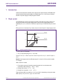
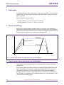
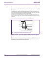
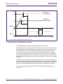
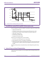
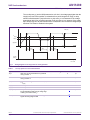
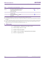
AN11489 PTN3460 power-up reset requirement Rev. 1 — 15 December 2014 Application note Document information Info Content Keywords PTN3460, PD_N, RST_N Abstract This document explains the power-up reset requirement for PTN3460 AN11489 NXP Semiconductors PTN3460 power-up reset requirement Revision history Rev Date Description 1 20141215 Initial version Contact information For more information, please visit: http://www.nxp.com For sales office addresses, please send an email to: [email protected] AN11489 Application note All information provided in this document is subject to legal disclaimers. Rev. 1 — 15 December 2014 © NXP Semiconductors N.V. 2014. All rights reserved. 2 of 11 AN11489 NXP Semiconductors PTN3460 power-up reset requirement 1. Introduction This document describes external power rail and reset requirements for PTN3460 when using an external single power supply on VDD(3v3) pins 13, 14, 38, 50 only or add an external 1v8 power supply to VDD(1v8) pins 6 and 45. 2. Single power The PTN3460 has a built-in Low-Dropout regulator (LDO) that can supply 1V8 for core use from an external 3V3 power supply, hence a user can only supply single 3V3 to PTN3460 pins 13, 14, 38 and 50. 1V8 will be output from pin 19 and feed into pins 6 and 45. EPS_N pin has an internal pull up resistor, this pin must left open for single supply mode. VDD(3V3) 3.0 V tstartup(VDD1V8) < 30 μs VDD(1V8) 1.7 V aaa-014262 Fig 1. Internal regulator start-up • EPS_N pin not connected • VDD(1V8) total decoupling Cdecap < 8 F total The 8 F is 4.7 F + 100 nF on pin 19 + 100 nF on pin 45 + 2.2 F + 100 nF on pin 6 + 10 % Remark: Input supply must be sufficiently high (3.0 V min) for LDO to provide a stable 1.8 V supply. LDO is used in 3 modes: 1. From power-up up to 90 ms after reset (the actual time is much shorter and somewhere within Tstartup): 1.86 V ... 2.02 V 2. During active modes: 1.7 V ... 1.9 V 3. During D3 or low power: 1.61 ... 1.77 V That means that LDO can make from 1.61 V up to 2.02 V depending on the power state LDO output (1.8 V): min 1.61 V, typ 1.8 V, max 2.02 V. AN11489 Application note All information provided in this document is subject to legal disclaimers. Rev. 1 — 15 December 2014 © NXP Semiconductors N.V. 2014. All rights reserved. 3 of 11 AN11489 NXP Semiconductors PTN3460 power-up reset requirement 3. Dual power The PTN3460 allows a user to supply both 3.3 V and 1.8 V externally. To use dual power supplies, EPS_N pin (56) must be pulled down with a 10K resistor. 1V8 power is fed into pins 6, 19 and 45. Recommended operating conditions: • Supply voltage (3.3 V): min 3.0 V, typ 3.3 V, max 3.6 V • Supply voltage (1.8 V): min 1.7 V, typ 1.8 V, max 1.9 V 4. Power sequencing At any point in time, the voltage on Vdd(3v3) pins 13, 14, 38 and 50, must always be higher than the voltage on Vdd(1v8) pins 6, 19 and 45. This sequence is always respected if the internal power regulator (LDO) is used but must be guaranteed by system designer if EPS_N is pulled LOW and the 1.8 V supply is provided externally. V VDD(3v3) VDD(3v3)>VDD(1v8) VDD(1v8) time vdd Fig 2. VDD(3V3) always greater than VDD(1V8) by 0.7 V minimum VDD(3V3) 5. Reset, power-down and power-on initialization The PTN3460 device has built-in reset circuitry that generates an internal reset signal after power-on. All the internal registers and state machines are initialized and the registers take default values. In addition, the PTN3460 has a dedicated control pin RST_N. This serves the same purpose as power-on reset, but without power cycling of the device/platform. PTN3460 starts up in a default condition after power-on or after RST_N is toggled from LOW to HIGH. The configuration pins are sampled at power-on, or external reset, or when returning from power-saving mode. AN11489 Application note All information provided in this document is subject to legal disclaimers. Rev. 1 — 15 December 2014 © NXP Semiconductors N.V. 2014. All rights reserved. 4 of 11 AN11489 NXP Semiconductors PTN3460 power-up reset requirement If PD_N function is not used it must be left unconnected. In the case PD_N is not connected the PTN3460 is designed NOT to need the RST_N pin and can be left unconnected as well. RST_N can be used as power-on reset without power cycling of the device/platform. An internal reset_n signal is active during power ramping up while RST_N can be left open. This internal signal cannot be measured back on the RST_N pin. RST_N pin has an internal pull-up and will therefore follow the 3V3 supply voltage. It is good practice to provide for RST_N control if EPS_N is LOW to use external 1.8 V supply. In case RST_N is used, it must be released after all supplies are within operating conditions. Device start-up time from power-on and RST_N = HIGH is 90 ms max. 1.7 V VDD(1V8) < 2.5 μs on-chip reset_n td(rstn_i2chz) < 20 μs I2C pins tstartup < 90 ms normal operation HPD aaa-014260 Fig 3. Start-up behavior with RST_N and PD_N unconnected Remark: Driving RST_N HIGH is not possible and forbidden during power-up because the ESD diodes will clamp the signal to the VDDIO+0.6 V. RST_N pin should be left at Tri-state level during power-up. Remark: PTN3460 I2C pins are not failsafe and cannot be connected to the SMBus if the SMBus has active communications during VDD33 supply switch ON. In the application there MUST be no MS_I2C traffic during supply rise-up. AN11489 Application note All information provided in this document is subject to legal disclaimers. Rev. 1 — 15 December 2014 © NXP Semiconductors N.V. 2014. All rights reserved. 5 of 11 AN11489 NXP Semiconductors PTN3460 power-up reset requirement [V] VDD(3v3) 3.0V t> 0 VDD(1v8) 1.7V t> 0 Supplies tw(rst) [V] [time] >10us RST_N [time] release Fig 4. Release RST_N after both 3V3 and 1V8 are stable 6. Power-down for Ultra Power Save The PTN3460 goes into power‐saving mode when PD_N is LOW. PD_N and RST_N can be controlled by the GPIO pins of system microcontroller. To leave power-saving mode, the system needs to drive PD_N back to HIGH, and issue a RST_N pulse for at least 10 us. The rising edge of PD_N can be aligned with RST_N edges (+/-100 ns) or occur while RST_N is LOW. RST_N and PD_N can be driven with open collector type pins without external pull-up resistors. If PD_N pin is open, the device will not enter power-saving mode. Once the device is in power-saving mode, the HPDRX pin will go LOW automatically and this can be used by the system to remove the 3.3 V supply, if required. The PTN3460 will not respect the Panel power-down sequence if PD_N is asserted LOW while video is being streamed to the display; the system is not supposed to toggle PD_N and RST_N pins asynchronously while the LVDS output is streaming video to the display panel, but instead will follow the panel powering sequence as described in datasheet. The time between PD_N going HIGH and HPD raised HIGH by the PTN3460 is also 90 ms max. AN11489 Application note All information provided in this document is subject to legal disclaimers. Rev. 1 — 15 December 2014 © NXP Semiconductors N.V. 2014. All rights reserved. 6 of 11 AN11489 NXP Semiconductors PTN3460 power-up reset requirement 1.7 V > 2.5 μs VDD(1V8) power saving mode normal operation PD_N td(rstn_i2chz) RST_N > 10 μs < 20 μs I2C pins tpwrsave tstartup HPD tstartup < 90 ms < 90 ms < 90 ms normal operation aaa-014261 Fig 5. Start-up behavior with RST_N and PD_N connected 7. Use GPIOs to control PD_N and RST_N from system side One code example to control PD_N and RST_N pulses from system side is shown below: • • • • • • Assert PD_N (make it low) PTN3460 is in power saving mode after 90 ms and HPD gets reset to LOW System waits until it wants to resume PNT3460's from power saving mode Assert RST_N (make it low) De-assert PD_N (make it high) De-assert RST_N (make it high) Only RST_N is used during power up, do the following: 1. Drive RST_N to LOW during power up in single supply 2. Not to drive RST_N to HI if 3.3 V supply is not guaranteed 3. Release RST_N from LOW to tri-state will remove the risk for driving HI while supply is not present. RST_N and PD_N has pull-up integrated to make pin high if driver is tri-state. Note: PD_N internal pull-up is only active shortly to avoid leakage during power-saving mode. 8. Internal Power-on Reset Characteristics Figure below shows a possible curve of the regulated VDD(1v8) voltage with dips at t2 to t3 and t4 to t5. AN11489 Application note All information provided in this document is subject to legal disclaimers. Rev. 1 — 15 December 2014 © NXP Semiconductors N.V. 2014. All rights reserved. 7 of 11 AN11489 NXP Semiconductors PTN3460 power-up reset requirement The on-chip reset_n (active LOW) starts active at t0. At t1, the voltage gets higher than the Vtrip(H) level and if this condition is maintained for a period longer than Thigh, a delay element will add another Tporp before the on-chip reset_n is de-asserted. If the voltage drops below Vtrip(L) for a period longer than Tlow, the reset_n is re-asserted. If the supply dip is shorter (eg. t4 to t5) the internal reset is not asserted. This means that voltage drops less than Tlow must be avoided in the system. VDD(1V8) Vtrip(H) Vtrip(L) supplies t0 t1 Thigh t2 Tporp t3 Tlow Thigh t4 [time] t5 Tporp on-chip reset_n [time] aaa-014263 Fig 6. Timing diagram of on-chip power-on reset generator Table 1. On-chip power-on reset characteristics Symbol Parameter Min Typ Max Unit Thigh time VDD(1V8) has to be above Vtrip(H) before reset_n will be ‘1’ - - 2 s Tlow time VDD(1V8) has to be below Vtrip(L) before reset_n will be ‘0’ - - 11 s Tporp minimal time reset_n will be ‘1’ after VDD(1V8) > Vtrip(H) 0.2 0.32 0.5 s Vtrip(H) HIGH trip level 1.0 1.2 1.6 V Vtrip(L) LOW trip level 0.95 1.1 1.4 V s ms Td(rstn_i2chz) delay time for I2C pins (SCL or SDA) to get into Hi impedance state from the rising edge of RST_N or internal reset_n - - 20[1] Tstartup time delay from RST_N or internal reset_n signal and rising edge of HPD - - 90[2] AN11489 Application note All information provided in this document is subject to legal disclaimers. Rev. 1 — 15 December 2014 © NXP Semiconductors N.V. 2014. All rights reserved. 8 of 11 AN11489 NXP Semiconductors PTN3460 power-up reset requirement Table 1. On-chip power-on reset characteristics …continued Symbol Parameter Min Typ Max Unit s Tpwrsave time delay from falling edge of PD_N and actual HPD falling edge while entering power-saving mode - - 90[3] Tw(rst) minimum requirement for external RST_N reset pulse width 10 - - s Tstartup(vdd1v8) internal 1.8 V regulator delay from VDD(3V3) within specification to VDD(1V8) within specification - - 30[4] s [1] This is based on simulations. In all cases seen in measurement this delay is actually much shorter. [2] This is a firmware deadline and the typical value can change with a FW update. The max timing has to be respected and checked at any FW update. [3] This delay is also defined by firmware. The FW polls for DP_N pin state at periods close to 50 ms and this makes the response fluctuate. [4] Based on worst-case measurements starting the regulator after VDD(3V3) is 3.0 V. In practical case the regulator starts at much lower supply level and this value can be considered 0 if input supply has rise time > 1 ms. 9. References AN11489 Application note [1] PTN3460 datasheet - PTN3460.pdf, Rev.4, March 12, 2014 [2] Reference Design, dp-lvds-rev1.15 pdf [3] AN11088 - PCB Layout Guideline [4] UM10492 - eDP to LVDS Bride IC Application Board User's Manual [5] AN11128 - Programming Guide All information provided in this document is subject to legal disclaimers. Rev. 1 — 15 December 2014 © NXP Semiconductors N.V. 2014. All rights reserved. 9 of 11 AN11489 NXP Semiconductors PTN3460 power-up reset requirement 10. Legal information 10.1 Definitions Draft — The document is a draft version only. The content is still under internal review and subject to formal approval, which may result in modifications or additions. NXP Semiconductors does not give any representations or warranties as to the accuracy or completeness of information included herein and shall have no liability for the consequences of use of such information. 10.2 Disclaimers Limited warranty and liability — Information in this document is believed to be accurate and reliable. However, NXP Semiconductors does not give any representations or warranties, expressed or implied, as to the accuracy or completeness of such information and shall have no liability for the consequences of use of such information. NXP Semiconductors takes no responsibility for the content in this document if provided by an information source outside of NXP Semiconductors. In no event shall NXP Semiconductors be liable for any indirect, incidental, punitive, special or consequential damages (including - without limitation - lost profits, lost savings, business interruption, costs related to the removal or replacement of any products or rework charges) whether or not such damages are based on tort (including negligence), warranty, breach of contract or any other legal theory. Notwithstanding any damages that customer might incur for any reason whatsoever, NXP Semiconductors’ aggregate and cumulative liability towards customer for the products described herein shall be limited in accordance with the Terms and conditions of commercial sale of NXP Semiconductors. Right to make changes — NXP Semiconductors reserves the right to make changes to information published in this document, including without limitation specifications and product descriptions, at any time and without notice. This document supersedes and replaces all information supplied prior to the publication hereof. Suitability for use — NXP Semiconductors products are not designed, authorized or warranted to be suitable for use in life support, life-critical or safety-critical systems or equipment, nor in applications where failure or malfunction of an NXP Semiconductors product can reasonably be expected to result in personal injury, death or severe property or environmental damage. NXP Semiconductors and its suppliers accept no liability for inclusion and/or use of NXP Semiconductors products in such equipment or applications and therefore such inclusion and/or use is at the customer’s own risk. Applications — Applications that are described herein for any of these products are for illustrative purposes only. NXP Semiconductors makes no representation or warranty that such applications will be suitable for the specified use without further testing or modification. Customers are responsible for the design and operation of their applications and products using NXP Semiconductors products, and NXP Semiconductors accepts no liability for any assistance with applications or customer product AN11489 Application note design. It is customer’s sole responsibility to determine whether the NXP Semiconductors product is suitable and fit for the customer’s applications and products planned, as well as for the planned application and use of customer’s third party customer(s). Customers should provide appropriate design and operating safeguards to minimize the risks associated with their applications and products. NXP Semiconductors does not accept any liability related to any default, damage, costs or problem which is based on any weakness or default in the customer’s applications or products, or the application or use by customer’s third party customer(s). Customer is responsible for doing all necessary testing for the customer’s applications and products using NXP Semiconductors products in order to avoid a default of the applications and the products or of the application or use by customer’s third party customer(s). NXP does not accept any liability in this respect. Export control — This document as well as the item(s) described herein may be subject to export control regulations. Export might require a prior authorization from competent authorities. Evaluation products — This product is provided on an “as is” and “with all faults” basis for evaluation purposes only. NXP Semiconductors, its affiliates and their suppliers expressly disclaim all warranties, whether express, implied or statutory, including but not limited to the implied warranties of non-infringement, merchantability and fitness for a particular purpose. The entire risk as to the quality, or arising out of the use or performance, of this product remains with customer. In no event shall NXP Semiconductors, its affiliates or their suppliers be liable to customer for any special, indirect, consequential, punitive or incidental damages (including without limitation damages for loss of business, business interruption, loss of use, loss of data or information, and the like) arising out the use of or inability to use the product, whether or not based on tort (including negligence), strict liability, breach of contract, breach of warranty or any other theory, even if advised of the possibility of such damages. Notwithstanding any damages that customer might incur for any reason whatsoever (including without limitation, all damages referenced above and all direct or general damages), the entire liability of NXP Semiconductors, its affiliates and their suppliers and customer’s exclusive remedy for all of the foregoing shall be limited to actual damages incurred by customer based on reasonable reliance up to the greater of the amount actually paid by customer for the product or five dollars (US$5.00). The foregoing limitations, exclusions and disclaimers shall apply to the maximum extent permitted by applicable law, even if any remedy fails of its essential purpose. Translations — A non-English (translated) version of a document is for reference only. The English version shall prevail in case of any discrepancy between the translated and English versions. 10.3 Trademarks Notice: All referenced brands, product names, service names and trademarks are the property of their respective owners. All information provided in this document is subject to legal disclaimers. Rev. 1 — 15 December 2014 © NXP Semiconductors N.V. 2014. All rights reserved. 10 of 11 AN11489 NXP Semiconductors PTN3460 power-up reset requirement 11. Contents 1 2 3 4 5 6 7 8 9 10 10.1 10.2 10.3 11 Introduction . . . . . . . . . . . . . . . . . . . . . . . . . . . . 3 Single power . . . . . . . . . . . . . . . . . . . . . . . . . . . 3 Dual power . . . . . . . . . . . . . . . . . . . . . . . . . . . . . 4 Power sequencing . . . . . . . . . . . . . . . . . . . . . . . 4 Reset, power-down and power-on initialization . . . . . . . . . . . . . . . . . . . . . . . . . . . . 4 Power-down for Ultra Power Save . . . . . . . . . . 6 Use GPIOs to control PD_N and RST_N from system side . . . . . . . . . . . . . . . . . . . . . . . . . . . . 7 Internal Power-on Reset Characteristics. . . . . 7 References . . . . . . . . . . . . . . . . . . . . . . . . . . . . . 9 Legal information. . . . . . . . . . . . . . . . . . . . . . . 10 Definitions . . . . . . . . . . . . . . . . . . . . . . . . . . . . 10 Disclaimers . . . . . . . . . . . . . . . . . . . . . . . . . . . 10 Trademarks. . . . . . . . . . . . . . . . . . . . . . . . . . . 10 Contents . . . . . . . . . . . . . . . . . . . . . . . . . . . . . . 11 Please be aware that important notices concerning this document and the product(s) described herein, have been included in section ‘Legal information’. © NXP Semiconductors N.V. 2014. All rights reserved. For more information, please visit: http://www.nxp.com For sales office addresses, please send an email to: [email protected] Date of release: 15 December 2014 Document identifier: AN11489