1
STMicroelectronics
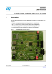
EVALSPEAr320CPU
SPEAr320 CPU
evaluation board
UM1015
User manual
Doc ID 18124 Rev 1
October 2010
www.st.com
BLANK
UM1015
User manual
EVALSPEAr320CPU
SPEAr320 CPU evaluation board
Introduction
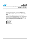
This document applies to revision 2.0 SPEAr320 CPU evaluation boards.
This board can be used to evaluate SPEAr320 microprocessors; the evaluation board kit
comprises one board, one serial cable interface, and one power supply.
CPU board features
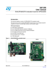
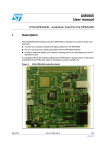
Figure 1.
■
SPEAr320 embedded MPU
■
Up to 2 Gbit DDR2 333 MHz (standard 128 Mbytes)
■
Up to 16 Mbyte Serial Flash memory (standard 8 Mbytes)
■
Two USB 2.0 full host port channels
■
One USB 2.0 host device port
■
One serial port (up to 115 baud)
■
JTAG Debug ports
SPEAr320 CPU evaluation board
Top
October 2010
Bottom
Doc ID 18124 Rev 1
3/38
www.st.com
Contents
UM1015
Contents
1
Getting started . . . . . . . . . . . . . . . . . . . . . . . . . . . . . . . . . . . . . . . . . . . . . . 7
1.1
Connections . . . . . . . . . . . . . . . . . . . . . . . . . . . . . . . . . . . . . . . . . . . . . . . . 7
1.2
Booting procedure . . . . . . . . . . . . . . . . . . . . . . . . . . . . . . . . . . . . . . . . . . . 7
2
Block diagram . . . . . . . . . . . . . . . . . . . . . . . . . . . . . . . . . . . . . . . . . . . . . . 8
3
Expansion connectors . . . . . . . . . . . . . . . . . . . . . . . . . . . . . . . . . . . . . . 11
4
Switch and jumper settings . . . . . . . . . . . . . . . . . . . . . . . . . . . . . . . . . . 15
4.1
Switch 1 settings . . . . . . . . . . . . . . . . . . . . . . . . . . . . . . . . . . . . . . . . . . . 15
4.2
Switch 2 settings . . . . . . . . . . . . . . . . . . . . . . . . . . . . . . . . . . . . . . . . . . . 16
4.3
Jumpers and connectors . . . . . . . . . . . . . . . . . . . . . . . . . . . . . . . . . . . . . 17
5
Board components . . . . . . . . . . . . . . . . . . . . . . . . . . . . . . . . . . . . . . . . . 18
6
Schematics . . . . . . . . . . . . . . . . . . . . . . . . . . . . . . . . . . . . . . . . . . . . . . . 22
7
Board layout . . . . . . . . . . . . . . . . . . . . . . . . . . . . . . . . . . . . . . . . . . . . . . . 31
8
Revision history . . . . . . . . . . . . . . . . . . . . . . . . . . . . . . . . . . . . . . . . . . . 32
A
4/38
8.1
Hardware revision history . . . . . . . . . . . . . . . . . . . . . . . . . . . . . . . . . . . . . 32
8.2
Document revision history . . . . . . . . . . . . . . . . . . . . . . . . . . . . . . . . . . . . 32
License agreements. . . . . . . . . . . . . . . . . . . . . . . . . . . . . . . . . . . . . . . . . 33
Doc ID 18124 Rev 1
UM1015
List of tables
List of tables
Table 1.
Table 2.
Table 3.
Table 4.
Table 5.
Table 6.
Table 7.
Table 8.
Table 9.
Switch SW1 bits [2:1] . . . . . . . . . . . . . . . . . . . . . . . . . . . . . . . . . . . . . . . . . . . . . . . . . . . . . . 9
CPU board extension connector J12 . . . . . . . . . . . . . . . . . . . . . . . . . . . . . . . . . . . . . . . . . 11
CPU board extension connector J13 . . . . . . . . . . . . . . . . . . . . . . . . . . . . . . . . . . . . . . . . . 13
Switch 1 (SoC functional configuration) . . . . . . . . . . . . . . . . . . . . . . . . . . . . . . . . . . . . . . . 15
Switch 1 (debug configuration) . . . . . . . . . . . . . . . . . . . . . . . . . . . . . . . . . . . . . . . . . . . . . . 15
Switch 1 (functional configuration) . . . . . . . . . . . . . . . . . . . . . . . . . . . . . . . . . . . . . . . . . . . 15
Switch 2 settings . . . . . . . . . . . . . . . . . . . . . . . . . . . . . . . . . . . . . . . . . . . . . . . . . . . . . . . . . 16
CPU board components . . . . . . . . . . . . . . . . . . . . . . . . . . . . . . . . . . . . . . . . . . . . . . . . . . . 18
Document revision history . . . . . . . . . . . . . . . . . . . . . . . . . . . . . . . . . . . . . . . . . . . . . . . . . 32
Doc ID 18124 Rev 1
5/38
List of figures
UM1015
List of figures
Figure 1.
Figure 2.
Figure 3.
Figure 4.
Figure 5.
Figure 6.
Figure 7.
Figure 8.
Figure 9.
Figure 10.
Figure 11.
Figure 12.
Figure 13.
Figure 14.
Figure 15.
6/38
SPEAr320 CPU evaluation board . . . . . . . . . . . . . . . . . . . . . . . . . . . . . . . . . . . . . . . . . . . . . 3
EVALSPEAr320CPU board block diagram. . . . . . . . . . . . . . . . . . . . . . . . . . . . . . . . . . . . . . 8
Serial cable setting . . . . . . . . . . . . . . . . . . . . . . . . . . . . . . . . . . . . . . . . . . . . . . . . . . . . . . . 9
86-pin connectors (J12 and J13) . . . . . . . . . . . . . . . . . . . . . . . . . . . . . . . . . . . . . . . . . . . . 11
Schematic interconnections . . . . . . . . . . . . . . . . . . . . . . . . . . . . . . . . . . . . . . . . . . . . . . . . 22
DDR interface schematic . . . . . . . . . . . . . . . . . . . . . . . . . . . . . . . . . . . . . . . . . . . . . . . . . . 23
USB interface schematic . . . . . . . . . . . . . . . . . . . . . . . . . . . . . . . . . . . . . . . . . . . . . . . . . . 24
USB power and optional part schematic. . . . . . . . . . . . . . . . . . . . . . . . . . . . . . . . . . . . . . . 25
Miscellaneous interfaces schematic . . . . . . . . . . . . . . . . . . . . . . . . . . . . . . . . . . . . . . . . . . 26
Power supply schematic . . . . . . . . . . . . . . . . . . . . . . . . . . . . . . . . . . . . . . . . . . . . . . . . . . . 27
Customization interface schematic . . . . . . . . . . . . . . . . . . . . . . . . . . . . . . . . . . . . . . . . . . . 28
Daughterboard interface schematic . . . . . . . . . . . . . . . . . . . . . . . . . . . . . . . . . . . . . . . . . . 29
Schematic revision history . . . . . . . . . . . . . . . . . . . . . . . . . . . . . . . . . . . . . . . . . . . . . . . . . 30
SPEAr320 CPU evaluation board layout (top view) . . . . . . . . . . . . . . . . . . . . . . . . . . . . . . 31
SPEAr320 CPU evaluation board layout (bottom view) . . . . . . . . . . . . . . . . . . . . . . . . . . . 31
Doc ID 18124 Rev 1
UM1015
1
Getting started
Getting started
Warning:
This board contains static sensitive devices.
The EVALSPEAr320CPU board is shipped in protective anti-static packaging. Do not submit
the board to high electrostatic potentials, and follow good practices for working with static
sensitive devices.
1.1
●
Wear an anti-static wristband. Wearing a simple anti-static wristband can help
prevent ESD from damaging the board.
●
Zero potential. Always touch a grounded conducting material before handling the
board, and periodically while handling it.
●
Use an anti-static mat. When configuring the board, place it on and anti-static mat to
reduce the possibility of ESD damage.
●
Handle only the edges. Handle the board by its edges only, and avoid touching board
components.
Connections
Refer to Figure 14 on page 31.
1.
Connect a serial cable from connector J17 (serial link) to a host PC.
2.
On the host PC running Windows or Linux, start the Terminal program.
3.
Connect the +5 V voltage adapter (supplied in the EVALSPEAR320CPU package) to
the J11 power voltage connector on the CPU board.
4.
Apply power to the board.
5.
The Terminal program displays a sequence of boot messages followed by the Linux
console prompt.
For more information, refer to user manual UM0844 Getting started with Linux for SPEAr,
available at www.st.com/spear.
1.2
Booting procedure
The SPEAr320 CPU evaluation board can boot a Linux kernel that has been pre-installed in
the serial NOR Flash.
At power on, the serial port outputs a brief header message with some uBoot information
(uBoot version, SDK version, and some internal hardware information). At this point you can
choose to:
●
Stop the system directly in uBoot: Press the spacebar on the host computer
keyboard before the boot delay time expires (default is 3 seconds).
●
Boot Linux: The system logs you in automatically as super user, and displays the
Linux shell prompt on the screen.
Doc ID 18124 Rev 1
7/38
Block diagram
UM1015
2
Block diagram
Figure 2.
EVALSPEAr320CPU board block diagram
2.0.1
Dynamic memory subsystem
The Dynamic memory subsystem comprises three major parts:
Memory chip
The SPEAr320 MPU supports up to 256 Mbytes of memory. Place and route is provided for
2 chips but only one has been populated. The memory used is a Micron DDR2 device, its
part number is MT47H64M16HR-3 and its size is 128 Mbits x 8 (16 Mbits x 8 x 8 banks).
Local power supply
The local power supply is based on a monolithic voltage regulator for the chip set and
DDR2/3 (PM6641). It is generated locally in order to minimize the layout impact and also to
avoid any noise injection between different subsystems.
Signal termination
A parallel termination is added on the clock lines to compensate, if needed, for the layout
dissymmetry. Two 100k ohm resistors are used for each line in order to obtain an
impedance of 50 ohms. All the other terminations are directly inside the pads (both on the
SPEAr320 MPU and the memory sides).
8/38
Doc ID 18124 Rev 1
UM1015
2.0.2
Block diagram
Static memory subsystem (Serial Flash memory)
The SPEAr320 MPU supports up to 16 Mbytes of Serial Flash memory. Place and route for
2 blocks of 8 Mbytes are provided on the board, but only one is populated. It is based on an
M25P64-VMF6P (Numonix) Serial Flash memory device.
Resistor R8 protects the Flash memory from any unwanted write access.
2.0.3
USB 2.0 subsystem
Host ports
The board has two host ports that are fully compliant with the USB 2.0 specification (two
controllers with one port each). This means that the two hosts can work in concurrent mode
with the maximum possible bandwidth. Each host has also full control of the VBUS supplied
by the ST2052 power switch that also provides over current protection in case of a short
circuit in the USB cable.
Device port
The board has one USB 2.0 device port.
2.0.4
Debug interface
The JTAG interface can be used for static debugging, which means that it is possible to set
a breakpoint, and when the system stops, verify the contents of the memory or registers, or
both, and modify them if needed.
To select the debug feature, set Switch SW1 bits [2:1].
Table 1.
Switch SW1 bits [2:1]
Bit 2
Bit 1
Description
0
0
No debug features available
0
1
The ARM JTAG is connected to J4
For more information on the ETM interface, refer to the trace box manufacturer’s
documentation (www.lauterbach.com, www.agilent.com, www.yokogawa.com).
2.0.5
Serial interface
One serial interface port is available. Typically used as an OS monitor, this port is available
on the J17 connector. It is possible to simulate a cross cable by changing the position of the
J22 jumpers.
Figure 3.
Serial cable setting
J22
2
4
1
3
Nul
Modem
Cable
J22
2
4
1
3
Doc ID 18124 Rev 1
Cross
Cable
9/38
Block diagram
2.0.6
UM1015
Real time clock (battery powered)
The real time clock (RTC) is powered by an external battery (3V) in order to prevent data
loss even if the main power supply is switched off.
2.0.7
General power supply
From a 5 V external AC/DC regulator power source, this block generates all the required
voltages as follows:
●
1.2V (Switching regulator PM6641) to supply the internal logic of the SPEAr320 MPU
●
1.8V (Switching regulator PM6641) for the DDR2 memory
●
2.5V (LDO regulator) for the analog portion of SPEAr320
●
3.3V (Switching regulator PM6641) to supply the other interfaces
A power monitor is also present to provide the general reset of the board.
2.0.8
Reset button
A manual reset button (P1) on the top of the board (see Figure 14 on page 31) resets the
microprocessor on the core board.
10/38
Doc ID 18124 Rev 1
UM1015
3
Expansion connectors
Expansion connectors
The CPU board has two 86-pin connectors (J12 and J13) that are used to extend the board.
On the board the connectors are horizontally center-aligned, and the distance between the
mechanical holes is 3400.00 th.
Table 2 lists connector J12 pins.
Table 3 on page 13 lists connector J13 pins.
Note:
Connector through hole pins (10 pins) are connected to GND
Figure 4.
Table 2.
86-pin connectors (J12 and J13)
75
1
76
2
CPU board extension connector J12
Pin
Description
Pin
Description
1
+1.8V
2
+5V
3
+1.8V
4
+5V
5
+1.8V
6
+5V
7
+1.8V
9
8
+5V
(1)
10
PL_GPIO44
(2)
PL_GPIO2 (RS232-TX LVTTL)
12
PL_GPIO39
13
RS232-TX
(3)
14
PL_GPIO40
15
RS232-RX(4)
16
PL_GPIO38
17
PL_GPIO42
18
PL_GPIO29
19
PL_GPIO43
20
PL_GPIO37
21
PL_GPIO34
22
PL_GPIO30
23
PL_GPIO33
24
PL_GPIO28
25
PL_GPIO16
26
PL_GPIO26
27
PL_GPIO24
28
PL_GPIO27
29
PL_GPIO20
30
PL_GPIO9
31
PL_GPIO23
32
PL_GPIO13
33
PL_GPIO18
34
PL_GPIO8
11
PL_GPIO3 (RS232-RX LVTTL)
Doc ID 18124 Rev 1
11/38
Expansion connectors
Table 2.
UM1015
CPU board extension connector J12 (continued)
Pin
Description
Pin
Description
35
PL_GPIO11
36
PL_GPIO6
37
PL_GPIO19
38
PL_GPIO4
39
PL_GPIO15
40
PL_GPIO5
41
PL_GPIO14
42
NC
43
PL_GPIO36
44
NC
45
PL_GPIO41
46
NC
47
PL_GPIO35
48
NC
49
PL_GPIO31
50
+2.5V
51
PL_GPIO32
52
+2.5V
53
PL_GPIO25
54
+2.5V
55
PL_GPIO22
56
+2.5V
57
PL_GPIO21
58
INRESET
59
PL_GPIO17
60
nRESET
61
PL_GPIO12
62
+1.2V
63
PL_GPIO10
64
+1.2V
65
PL_GPIO7
66
+1.2V
67
PL_GPIO1
68
+1.2V
69
PL_GPIO0
70
+3.3V
71
NC
72
+3.3V
73
NC
74
+3.3V
75
NC
76
+3.3V
78
77
79
81
80
GND
(5)
82
83
84
85
86
GND(5)
1. If J20 Jumper is set to pin2-3, otherwise NC.
2. If J21 Jumper is set to pin2-3, otherwise NC.
3. If J22 Jumper is set to pin2-4 and pin1-3, otherwise RS232-RX.
4. If J22 Jumper is set to pin2-4 and pin1-3, otherwise RS232-TX.
5. Physically connected to the internal metal plane of the connector. Pins 77 through 81 and 82 through 86
are shorted together.
12/38
Doc ID 18124 Rev 1
UM1015
Expansion connectors
Table 3.
CPU board extension connector J13
Pin
Description
Pin
Description
1
PL_GPIO47
2
+3.3V
3
PL_GPIO49
4
PL_GPIO63
5
PL_GPIO56
6
PL_GPIO46
7
PL_GPIO58
8
PL_GPIO57
9
PL_GPIO64
10
PL_GPIO61
11
PL_GPIO45
12
PL_GPIO66
13
PL_GPIO48
14
PL_GPIO69
15
PL_GPIO50
16
PL_GPIO72
17
PL_GPIO55
18
PL_GPIO73
19
PL_GPIO59
20
PL_GPIO70
21
PL_GPIO60
22
PL_GPIO67
23
PL_GPIO65
24
PL_GPIO71
25
PL_GPIO62
26
PL_GPIO75
27
PL_GPIO68
28
PL_GPIO82
29
PL_GPIO52
30
PL_GPIO76
31
PL_GPIO53
32
PL_GPIO85
33
PL_GPIO51
34
PL_GPIO87
35
PL_GPIO54
36
PL_GPIO95
37
PL_GPIO74
38
PL_GPIO79
39
PL_GPIO77
40
PL_GPIO94
41
PL_GPIO78
42
ADC VREFN
43
PL_GPIO81
44
AIN0
45
PL_GPIO80
46
GND
47
PL_GPIO84
48
AIN1
49
PL_GPIO83
50
GND
51
PL_GPIO86
52
AIN2
53
PL_GPIO91
54
GND
55
PL_GPIO90
56
AIN3
57
PL_GPIO96
58
GND
59
PL_GPIO88
60
AIN4
61
PL_GPIO89
62
GND
63
PL_GPIO92
64
AIN5
65
PL_GPIO93
66
GND
67
PL_GPIO97
68
AIN6
69
PL_CLK4
70
GND
Doc ID 18124 Rev 1
13/38
Expansion connectors
Table 3.
UM1015
CPU board extension connector J13 (continued)
Pin
Description
Pin
Description
71
PL_CLK3
72
AIN7
73
PL_CLK2
74
GND
75
PL_CLK1
76
ADC VREFP
77
78
79
80
81
GND(1)
82
83
84
85
86
GND(1)
1. Physically connected to the internal metal plane of the connector. Pins 77 through 81 and 82 through 86
are shorted together.
14/38
Doc ID 18124 Rev 1
UM1015
Switch and jumper settings
4
Switch and jumper settings
4.1
Switch 1 settings
Table 4.
Switch 1 (SoC functional configuration)
Bit
Description
1
Test – see Debug configuration below
2
Reserved
3
Reserved
4
Reserved
5
Reserved
6
BootSel – see Debug configuration below
Table 5.
Switch 1 (debug configuration)
Test bit
Debug configuration
2
1
0
0
Normal Mode (No debug enabled)
0
1
ARM1 JTAG connected to J4
1
0
Reserved
Table 6.
Switch 1 (functional configuration)
Test bit
Functional configuration
Note:
6
5
4
3
1
0
1
1
Configuration 3
When Switch SW1-x is in the ON position, the bit value is 0. When Switch 1 is in the OFF
position, the bit value is 1.
Bits 3, 4, 5 and 6 enable you to set the Functional configuration. The default configuration is
Configuration 3. For other configurations, refer to the SPEAr320 user manual available at
www.st.com/spear.
Doc ID 18124 Rev 1
15/38
Switch and jumper settings
4.2
Switch 2 settings
Table 7.
Switch 2 settings
Boot from
Note:
UM1015
SW2-1 SW2-2 SW2-3 SW2-4 SW2-5 SW2-6 SW2-7 SW2-8
USB_BOOT
Off
On
Off
On
Off
On
Off
On
ETH (parameter from I2C
ROM)
On
Off
Off
On
Off
On
Off
On
ETH (parameter from SPI
ROM)
Off
On
On
Off
Off
On
Off
On
Serial NOR (default setting)
On
Off
On
Off
Off
On
Off
On
Parallel NOR 8 (EMI with ACK)
Off
On
Off
On
On
Off
Off
On
Parallel NOR 16 (EMI with
ACK)
On
Off
Off
On
On
Off
Off
On
Parallel NAND 8
Off
On
On
Off
On
Off
Off
On
Parallel NAND 16
On
Off
On
Off
On
Off
Off
On
Reserved for SPI
Off
On
Off
On
Off
On
On
Off
Reserved for I²C
On
Off
Off
On
Off
On
On
Off
UART_BOOT
Off
On
On
Off
Off
On
On
Off
BootROM bypass
On
Off
On
Off
Off
On
On
Off
Parallel NOR 8 (EMI without
ACK)
Off
On
Off
On
On
Off
On
Off
Parallel NOR 16 (EMI without
ACK)
On
Off
Off
On
On
Off
On
Off
Reserved
Off
On
On
Off
On
Off
On
Off
Reserved
On
Off
On
Off
On
Off
On
Off
If SW2-1 and SW2-2 are both off, B0 (pin PL_GPIO51) is in HiZ state, and can be controlled
from the application board.
If SW2-3 and SW2-4 are both off, B1 (pin PL_GPIO52) is in HiZ state, and can be controlled
from the application board.
If SW2-5 and SW2-6 are both off, B2 (pin PL_GPIO53) is in HiZ state, and can be controlled
from the application board.
If SW2-7 and SW2-8 are both off, B3 (pin PL_GPIO54) is in HiZ state, and can be controlled
from the application board.
SW2-1 and SW2-2 on: invalid condition
SW2-3 and SW2-4 on: invalid condition
SW2-5 and SW2-6 on: invalid condition
SW2-7 and SW2-8 on: invalid condition
16/38
Doc ID 18124 Rev 1
UM1015
4.3
Switch and jumper settings
Jumpers and connectors
The jumpers and connectors numbered below refer to the CPU board schematics (available
on www.st.com/spear).
Sheet 4
●
Connector J3 is a standard 20-pin 2.54 mm connector used for JTAG connections.
●
Jumper J5 enables the power supply to the Real Time Clock block.
If jumper J5 is closed, the RTC is powered (standard).
●
Connector J10 is a 2 vie 1.25 mm pitch connector for battery back-up with cable.
Sheet 5
●
Connector J11 is a standard power connector for the ADC power supply with a 2.1-mm
central pitch.
Sheet 6
●
Jumpers J6, J7, J8 and J9 are serial jumpers for the SPEAr power rail.
All jumpers MUST be closed. This configuration is used for power measurements.
Sheet 7
●
Jumper J22 is a 4-pin symmetric IDC (or strip) connector that switches RX and TX
signals for different types of RS-232 cables(a):
–
Two pins are connected to the ST3232 Receive/Transmit side.
–
Two pins are connected to the RS-232 Receive/Transmit connector side.
●
Connector J17 is a connector for standard IDC-to-DSUB converters.
●
Jumper J20 switches between RS-232 transmit signals or GPIO2:
●
–
If jumper is on pins 1 and 2, pin PL_GPIO2 is connected to U12 (ST3232) and the
COM0 is available on J17.
–
If jumper is on pins 2 and 3, pin PL_GPIO2 is connected to the expansion
connector J12 pin 9. In this case the COM0 is available on CN13.
Jumper J21 switches between RS-232 receive signals or GPIO3:
–
If jumper is on pins 1 and 2, pin PL_GPIO3 is connected to U12 (ST3232) and the
COM0 is available on J17.
–
If jumper is on pins 2 and 3, pin PL_GPIO3 is connected to the expansion
connector J12 pin 11. In this case the COM0 is available on CN13.
a. With 2 jumpers (inserted) it is possible to switch between two jumper inserted vertically and two jumpers
inserted horizontally. This enables the serial cable (null modem cable) to be adapted to the CPU board.
Doc ID 18124 Rev 1
17/38
Board components
UM1015
5
Board components
Table 8.
CPU board components
Component
Designator
Footprint
Description
Capacitor
C1 C2 C3
C4 C5 C6
C7 C8 C9
C10 C11
C12 C13
C14 C15
C16 C17
C18 C19
C20 C21
C22 C23
C24 C25
C26 C27
C28 C29
C30 C31
0402
C32 C33
C34 C35
C36 C37
C38 C39
C40 C41
C42 C43
C44 C45
C46 C47
C48 C49
C50 C56
C57 C58
C59 C60
C99 C100
C101 C102
Ceramic capacitor 0.1uF 10% 10V X5R 0402
Resistor
R42 R43
R44 R45
R46 R47
R48 R50
0603
Resistor 0603 0 ohm
Resistor
R30 R31
R32 R33
R34 R35
R36 R37
R38 R72
R73 R74
0603
Resistor 0603 1k ohm 1% 0.1W
Inductor
L3
LPS3.9X3.9
Power Inductor 1uH 1.7A 3.9x3.9mm SMD
Capacitor
C89
0603
Ceramic capacitor 2.2nF 10% 50V X7R 0603
Inductor
L1 L2
LPS3.9X3.9
Power Inductor 2.2uH 1.2A 3.9x3.9mm SMD
Resistor
R59 R60
0603
Resistor 0603 4.3 ohm 1% 0.1W
Resistor
R27 R28
0603
Resistor 0603 4.7k ohm 1% 0.1W
18/38
Doc ID 18124 Rev 1
UM1015
Table 8.
Board components
CPU board components (continued)
Component
Designator
Footprint
Description
Resistor
R10 R11
R12 R13
R14 R15
R16 R17
R18 R19
R20 R21
R22 R23
R24 R25
R26
0603
Resistor 0603 10k ohm 1% 0.1W
Capacitor
C75 C76
C77
0603
Ceramic capacitor 10 nF 10% 50V X7R 0603
Capacitor
C61 C62
C63 C64
C65 C66
C67 C68
C69 C70
C71 C72
C73 C74
C98
0805
Ceramic capacitor 10uF 10% 10V X5R 0805
Resistor
R68
0603
Resistor 0603 15k ohm 1% 0.1W
Capacitor
C78 C79
0603
Ceramic capacitor 15pF 5% 50V COG 0603
Capacitor
C87 C88
C91
0603
Ceramic capacitor 22nF 10% 50V X7R 0603
Capacitor
C93
1206
Ceramic capacitor 22 uF Y5V -20+80% 6.3V 1206
Crystal oscillator
Y2
RAD-HC49
Crystal Oscillator 24MHz 30ppm through-hole
Resistor
R70
0603
Resistor 0603 27k ohm 1% 0.1W
Crystal oscillator
Y1
XT38T
Crystal Oscillator 32.768KHz 20ppm d2x6mm
Capacitor
C92
0603
Ceramic capacitor 33 nF 10% 50V X7R 0603
Capacitor
C80 C81
0603
Ceramic capacitor 33pF 5% 50V COG 0603
Resistor
R29
0805
Resistor 0805 43.2 ohm 0.1% 0.1W
Resistor
R69
0603
Resistor 0603 47k ohm 1% 0.1W
Capacitor
C82 C83
C84 C85
C86 C94
C95 C96
C97
3528+
Tantalium Capacitor 47uF 10% 10V 3528-21
Resistor
R49
0603
Resistor 0603 56k ohm 1% 0.1W
Resistor
R62 R63
R64 R65
R66 R67
0603
Resistor 0603 68k ohm 1% 0.1W
Resistor
R61
0603
Resistor 0603 75k ohm 1% 0.1W
Resistor
R2 R3 R4
R5 R6 R7
0603
Resistor 0603 100 ohm 1% 0.1W
Doc ID 18124 Rev 1
19/38
Board components
Table 8.
UM1015
CPU board components (continued)
Component
Designator
Footprint
Description
Resistor
R1 R53
0805
Resistor 0805 121k ohm 0.1% 0.1W
Resistor
R55 R56
R57
0603
Resistor 0603 150 Kohm 1% 0.1W
Resistor
R39 R40
0603
Resistor 0603 150 ohm 1% 0.1W
Resistor
R75
0603
Resistor 0603 330 ohm 1% 0.1W
Resistor
R58
0603
Resistor 0603 390k ohm 1% 0.1W
Resistor
R8 R9
0603
Resistor 0603 470 ohm 1% 0.1W
Capacitor
C90
0603
Ceramic capacitor 470 pF 10% 50V X7R 0603
Resistor
R41
0603
Resistor 0603 680 ohm 1% 0.1W
Battery
U8
BR2032
BATT BR2032: Coin type Lithium batterie 3V straight d20mm
Ferrite bead
FB3 FB4
FB5 FB6
FB7
0805
Ferrite Murata BLM21BD601SN1D
600 ohm/100MHz 200mA 0.35hm 0805
Diode
D3
SOT23
Hi speed switching dual diode 200mA 70V
D BAV70
DC power socket
J11
DPS2.5MM
DC Power socket 2.5mm
DIP switch
SW1
SWM-6X-SMD
Surface mount 6-way micro dip switch pitch1.27mm
DIP switch
SW2
SWM-8X-SMD
Surface mount 8-way micro dip switch pitch1.27mm
Ferrite bead
FB8 FB9
FB12 FB13
0603
FB14 FB15
FB10 FB16
Ferrite 2506033007Y0 SMD 400mA
LED
D5 D6 D7
D8 D9
0805P
LED SMD 2,0 x 1,25mm Superbright Green
Connector
J17
IDC5X2MD
IDC 5X2 MD POL; IDC header 10pin p2.54mm straight male
polarized
Connector
J3
IDC10X2MD
IDC header 20pin p2.54mm straight male polarized
LED
D1 D2
0805P
Led SMD 2,0 x 1,25mm Superbright red
Memory
U5
SO16
M25P64; Numonix 64Mbit SPI Serial Flash Memory 3.3V
16pin SO
Diode
Z1
SOD123-C425
MMSZ5232BT1; Zener Diode 5.6V 0.5W
Connector
J10
MLX-1.25MM-M
MOLEX 1.25MM 2W M; Molex 1.25mm 2way male straight
SDRAM
U2 U3
FBGA84
MT47H64M16HR3; MICRON DDR2 128MB 1.8V FBGA84
Transistor
Q1
SOT23
NPN BC848; NPN transistor 30Vbc 5Vbe 100mA
Transistor
Q2 Q3
SOT23
NPN PDTD123Y; Digital transistor NPN Rb 2.2K Re 10K
500mA 250mW SOT23
Pad
PD1
PDX280H60SQ
PADX2-80H60; Two square pad 80x80mils 60mils Hole
100mils pitch
Resistor
R54
0603
R 0603 0 OHM; Resistor 0603 0 ohm
20/38
Doc ID 18124 Rev 1
UM1015
Table 8.
Board components
CPU board components (continued)
Component
Designator
Footprint
Description
Connector
J12 J13
MIS-038
SAMTEC-MIS-038; SAMTEC MIS series 76pin 0.64mm pitch
Rectifier
D4
DPAK
SCR TS420-B_1; Schottky barrier rectifier 1A 60V SMD
Embedded
microprocessor
U1
SG-BGA-6004
SPEAR300; STmicroelectronics Spear330
Power distribution
U4
switch
SO8
ST2052; STm Current limited power distribution switches
RS-232 driver
and receiver
U12
SO16
ST3232C; STm RS-232 driver and receiver
Voltage regulator
U9
SOT223
ST LD1117S25TR; STm low drop fixed positive voltage
regulator 2.5V 800mA
Reset circuit
U7
SOT143-4
STM811; STm Reset generator and power monitor 3.3V
SOT143-4
Voltage regulator
U10
VFQFPN-48
ST PM6641; STm DDR2/3 Voltage Regulator 48pin VFQFPN
Connector
J5 J6 J7
J8 J9
2X1-2.54-MD
STRIP-2X1-2.54-MD; Strip vertical male 2X1 2.54mm
Connector
J22
2X2-2.54-MD
STRIP-2X2-2.54-MD; Strip vertical male 2X2 2.54mm
Connector
J20 J21
3X1-2.54-MD
STRIP-3X1; Strip vertical male 3X1 2.54mm
Overvoltage
protection
U16
TDFN-10
ST STBP120C; STm overvoltage protection device Vout max
5.5V
ESD
protection circuit
U13 U14
U15
SOT23-6L
ST USBLC6-2SC6; STm USB 2.0 ESD protections
Switch
P1
SW-PB-SMD6x6.6
SW-PB-SMD; Mechanical key switch SMD 6x6.6mm
h4.3mm
Connector
J2
USB-A-RA-DB
USB A-TYPE RA DOUBLE; USB double A-type connector
right angle
Connector
J1
USB-B-RA-1
USB B-TYPE RA SH; USB B-type connector right angle
Ferrite bead
FB1 FB2
0805
WURTH 742792023; Ferrite Wurth 742792023 SMD 500mA
Doc ID 18124 Rev 1
21/38
Schematics
6
UM1015
Schematics
Figure 5.
Schematic interconnections
02 - DDR Interface
02 - DDR Interface.SchDoc
VREF
03 - USB Interface
03 - USB Interface.SchDoc
ADC_VREFP
ADC_VREFN
04 - Misc
04 - Misc.SchDoc
ADC_VREFP
ADC_VREFN
AIN[0..7]
INRESET
nRESET
05 - Power
05 - Power.SchDoc
VREF
nRESET
VREF
06 - PL_GPIO
06 - PL_GPIO.SchDoc
PL_GPIO[0..97]
PL_CLK[1..4] PL_GPIO[0..97]
PL_CLK[1..4]
07 - OutCon
07 - OutCon.SchDoc
AIN[0..7]
INRESET
ADC_VREFN
ADC_VREFP
PL_GPIO[0..97]
PL_CLK[1..4]
nRESET
AIN[0..7]
INRESET
In Figure 5:
22/38
●
02: DDR2 intrface and power
●
03: USB interface
●
04: Miscellaneous (serial flash, RTC power, boot options, JTAG, reset)
●
05: Power supply
●
06: PL_GPIO interface, extended boot options
●
07: Daughterboard and UART connectors
Doc ID 18124 Rev 1
DDR interface schematic
8
7
6
5
4
3
2
UM1015
Figure 6.
1
ADDR[0..13]
DATA[0..15]
4
4
CLK_EN
CLK
nCLK
VREF
U7
T9
U9
L8
K3
K7
L7
P10
1
2
TP_diff
VREF
C99
COMP_2V5_REXT
CLK_EN K2
J8
CLK
K8
nCLK
0.1 uF X5R 10V
P4
ODT1
R1
COMP_2V5_GND
121 Kohm 1%
Place close to pins
R4
K9
R3
R7
E2
A2
Spear300
J7
P9
N1
J3
E3
A3
2
LDM
UDM
VREF
LDQS
nLDQS
UDQS
nUDQS
VDD1V8_1
VDD1V8_2
VDD1V8_3
VDD1V8_4
VDD1V8_5
nCS
nWE
nRAS
nCAS
VDDL1V8
VDDQ1V8_1
VDDQ1V8_2
VDDQ1V8_3
VDDQ1V8_4
VDDQ1V8_5
VDDQ1V8_6
VDDQ1V8_7
VDDQ1V8_8
VDDQ1V8_9
VDDQ1V8_10
CKE
CLK
nCLK
ODT
RFU1
RFU2
NC1
NC2
VSSDL
VSS1
VSS2
VSS3
VSS4
VSS5
MT47H64M16HR3,NC
VSSQ1
VSSQ2
VSSQ3
VSSQ4
VSSQ5
VSSQ6
VSSQ7
VSSQ8
VSSQ9
VSSQ10
L1
L3
L2
BA2
BA1
BA0
J2
Place close to pin
C2
VREF
A1
E1
M9
R1
J9
1.8V_SP
Place close to pin
J1
A9
C1
C3
C7
C9
E9
G1
G3
G7
G9
C1
1.8V_SP
0.1 uF X5R 10V
DQM0
DQM1
F3
B3
DQS0
nDQS0
DQS1
nDQS1
F7
E8
B7
A8
nCS0
nWE
nRAS
nCAS
L8
K3
K7
L7
CLK_EN K2
J8
CLK
K8
nCLK
K9
ODT0
R3
R7
E2
A2
1.8V_SP
A7
B2
B8
D2
D8
E7
F2
F8
H2
H8
J7
P9
N1
J3
E3
A3
DATA8
DATA9
DATA10
DATA11
DATA12
DATA13
DATA14
DATA15
LDM
UDM
8MBx16 MT47H64M16HR-3
nCS1
nWE
nRAS
nCAS
1
2
CLK_EN
CLK
nCLK
GATE_OPEN0
GATE_OPEN1
DQM0
DQM1
F7
E8
B7
A8
BA2
BA1
BA0
C8
C2
D7
D3
D1
D9
B1
B9
ADDR0
ADDR1
ADDR2
ADDR3
ADDR4
ADDR5
ADDR6
ADDR7
ADDR8
ADDR9
ADDR10
ADDR11
ADDR12
ADDR13
BA2
BA1
BA0
VREF
LDQS
nLDQS
UDQS
nUDQS
VDD1V8_1
VDD1V8_2
VDD1V8_3
VDD1V8_4
VDD1V8_5
nCS
nWE
nRAS
nCAS
VDDL1V8
VDDQ1V8_1
VDDQ1V8_2
VDDQ1V8_3
VDDQ1V8_4
VDDQ1V8_5
VDDQ1V8_6
VDDQ1V8_7
VDDQ1V8_8
VDDQ1V8_9
VDDQ1V8_10
CKE
CLK
nCLK
ODT
RFU1
RFU2
NC1
NC2
VSSDL
VSS1
VSS2
VSS3
VSS4
VSS5
MT47H64M16HR3
VSSQ1
VSSQ2
VSSQ3
VSSQ4
VSSQ5
VSSQ6
VSSQ7
VSSQ8
VSSQ9
VSSQ10
ADDR0
ADDR1
ADDR2
ADDR3
ADDR4
ADDR5
ADDR6
ADDR7
ADDR8
ADDR9
ADDR10
ADDR11
ADDR12
ADDR13
L1
L3
L2
BA2
BA1
BA0
J2
VREF
Place close to pin
A1
E1
M9
R1
J9
C4
0.1 uF X5R 10V
1.8V_SP
Place close to pin
J1
A9
C1
C3
C7
C9
E9
G1
G3
G7
G9
C3
1.8V_SP
3
WURTH 742792023
R10
R14
DQM0 U12
DQM1 T14
DQS0
nDQS0
DQS1
nDQS1
TP30
DQS1
nDQS1
ODT0
ODT1
F3
B3
DATA9
DATA12
DATA11
DATA14
DATA13
DATA8
DATA15
DATA10
DATA0
DATA1
DATA2
DATA3
DATA4
DATA5
DATA6
DATA7
M8
M3
M7
N2
N8
N3
N7
P2
P8
P3
M2
P7
R2
R8
FB2
T3
T4
ODT0
ODT1
DQM0
DQM1
BA0
BA1
BA2
DATA8
DATA9
DATA10
DATA11
DATA12
DATA13
DATA14
DATA15
G8
G2
H7
H3
H1
H9
F1
F9
0.1 uF X5R 10V
DQS1 U15
nDQS1 T15
DQS0
nDQS0
C8
C2
D7
D3
D1
D9
B1
B9
DATA4
DATA5
DATA3
DATA0
DATA1
DATA2
DATA6
DATA7
MICRON DDR2
DQS0 U10
nDQS0 T10
nCS0
nCS1
P7
P8
R8
DATA12
DATA9
DATA14
DATA11
DATA8
DATA13
DATA10
DATA15
ADDR0
ADDR1
ADDR2
ADDR3
ADDR4
ADDR5
ADDR6
ADDR7
ADDR8
ADDR9
ADDR10
ADDR11
ADDR12
ADDR13
ADDR0
ADDR1
ADDR2
ADDR3
ADDR4
ADDR5
ADDR6
ADDR7
ADDR8
ADDR9
ADDR10
ADDR11
ADDR12
ADDR13
WURTH 742792023
P9
R9
BA0
BA1
BA2
ADDR0
ADDR1
ADDR2
ADDR3
ADDR4
ADDR5
ADDR6
ADDR7
ADDR8
ADDR9
ADDR10
ADDR11
ADDR12
ADDR13
M8
M3
M7
N2
N8
N3
N7
P2
P8
P3
M2
P7
R2
R8
FB1
nCS0
nCS1
nRAS
nCAS
nWE
T2
T1
U1
U2
U3
U4
U5
T5
R5
P5
P6
R6
T6
U6
R7
U3
U2
DATA0
DATA1
DATA2
DATA3
DATA4
DATA5
DATA6
DATA7
0.1 uF X5R 10V
U8
T8
T7
ADDR0
ADDR1
ADDR2
ADDR3
ADDR4
ADDR5
ADDR6
ADDR7
ADDR8
ADDR9
ADDR10
ADDR11
ADDR12
ADDR13
ADDR14
G8
G2
H7
H3
H1
H9
F1
F9
8MBx16 MT47H64M16HR-3
nRAS
nCAS
nWE
DATA0
DATA1
DATA2
DATA3
DATA4
DATA5
DATA6
DATA7
DATA8
DATA9
DATA10
DATA11
DATA12
DATA13
DATA14
DATA15
DATA5
DATA4
DATA0
DATA3
DATA2
DATA1
DATA7
DATA6
MICRON DDR2
Doc ID 18124 Rev 1
3
P11
R11
T11
U11
T12
R12
P12
P13
T17
T16
U17
U16
U14
U13
T13
R13
Spear300
DATA0
DATA1
DATA2
DATA3
DATA4
DATA5
DATA6
DATA7
DATA8
DATA9
DATA10
DATA11
DATA12
DATA13
DATA14
DATA15
DDR2 Interface
U1B
1.8V_SP
A7
B2
B8
D2
D8
E7
F2
F8
H2
H8
2
REF1
1.8V_SP
FIDUCIAL
1.8V_SP
1.8V_SP
REF2
R4
100 Ohm
nCLK
C19
VREF
C20
R5
100 Ohm
1
VREF
C16
C17
FIDUCIAL
Place close to DDR2 Chip
FIDUCIAL
R9
470 Ohm
1.8V_SP
1.8V_SP
1
C62
10 uF X5R 10V
Project
Title
23/38
5
4
3
2
CPU Board
Rev
DDR2 interface
Date:
6
Board
Spear300
20 Oct 2009
Code
2.3
Sheet
1
2
of
8
Schematics
C61
10 uF X5R 10V
7
FIDUCIAL
REF7
C18
REF8
Place close to DDR2 Chip
Place close to LAST DDR2 Chip
8
0.1 uF X5R 10V
C15
0.1 uF X5R 10V
C14
0.1 uF X5R 10V
C13
0.1 uF X5R 10V
C12
0.1 uF X5R 10V
C11
0.1 uF X5R 10V
C10
0.1 uF X5R 10V
C9
0.1 uF X5R 10V
C8
0.1 uF X5R 10V
C7
0.1 uF X5R 10V
C6
0.1 uF X5R 10V
C5
0.1 uF X5R 10V
R8
470 Ohm
0.1 uF X5R 10V
CLK
R3
100 Ohm
0.1 uF X5R 10V
0.1 uF X5R 10V
R2
100 Ohm
0.1 uF X5R 10V
1.8V_SP
USB interface schematic
USB Interface
C75
3.3V_SP
FB3
10 nF X7R 50V
R10
BLM21BD601SN1D
5
6
HOST0_VBUS
HOST0_DM
HOST0_DP
FERRITE-0603
FB16
J3
K2
K1
HOST0_OVERCUR H4
USB_DEV_VBUS
USB_DEV_DM
USB_DEV_DP
USB_DEV_VDD2V5
USB_HOST0_VDD2V5
USB_HOST1_VDD2V5
USB_HOST0_VBUS
USB_HOST0_DM
USB_HOST0_DP
1
2
3
4
HOST0_5V
HOST0_INF_DM
HOST0_INF_DP
H3
HOST1_DM
HOST1_DP
H2
H1
5
6
7
8
HOST1_5V
HOST1_INF_DM
HOST1_INF_DP
9
Shield1 10
Shield2 11
Shield3 12
Shield4
USB A-TYPE RA DOUBLE
FB9
TP1
R29
TP-TH
L4
BLM21BD601SN1D
2.5V_SP
FB5
BLM21BD601SN1D
FB6
BLM21BD601SN1D
M3 USB_VDD1V2
USB_HOST1_VBUS USB Interface
USB_HOST1_DM
USB_HOST1_DP
C21
C22
C23
C24
C25
FB7
BLM21BD601SN1D
1.2V_SP
USB_HOST1_OVERCUR
USB_COMMON_VSSac
USB_DVSS
K5
43.2 Ohm 1%
Doc ID 18124 Rev 1
H1-Vbus
A H1-DM
H1-DP
H1-GND
B_DEV_VDD2V5
B_HOST_VDD2V5
Spear300
HOST1_VBUS
HOST1_OVERCURJ4
H0-Vbus
H0-DM
H0-DP
H0-GND
USB_DVDD1V2
N1
L2
K3
USB_HOST0_OVERCUR
FERRITE-0603
J2
USB_DEV_VDD3V3
USB_HOST0_VDD3V3
USB_HOST1_VDD3V3
0.1 uF X5R 10V
M2
M1
0.1 uF X5R 10V
USB_DEV_DM
USB_DEV_DP
4.7 Kohm
B_DEV_VDD3V3
B_HOST_VDD3V3
0.1 uF X5R 10V
USB_DEV_5V
USB_DEV_INF_DM
USB_DEV_INF_DP
N3
K4
J1
0.1 uF X5R 10V
Shield1
Shield2
USB B-TYPE RA
FB8
1
2
3
4
USB_DEV_VBUS G3
R27
0.1 uF X5R 10V
B
Vb
D-D+
Gn
FB4
U1C
10 Kohm
J1
Schematics
24/38
Figure 7.
USB_TXR_TUNE
USB_DEV_VSSa
USB_HOST0_VSSa
USB_ANALOG_TEST USB_HOST1_VSSa
L3
L5
N2
L1
J2
Spear300
FERRITE-0603
FB10
FERRITE-0603
USB Power
UM1015
UM1015
USB power and optional part schematic
USB Power
3.3V
5V
2
3
4
HOST0_VBUS
HOST1_VBUS
U4
IN
OUT1
OUT2
EN1
EN2
nOC1
nOC2
7
6
HOST0_5V
HOST1_5V
8
5
R30
1 Kohm
R31
1 Kohm
D1
Led red
D2
Led red
R39
150 Ohm
R40
150 Ohm
HOST0_OVERCUR
HOST1_OVERCUR
ST2052GND 1
ST2052
5V
C26
0.1 uF X5R 10V
Optional part
0.1 uF X5R 10V
USB_DEV_DM
USB_DEV_DP
0.1 uF X5R 10V
1
3
U13
I/O1 I/O1
I/O2 I/O2
USBLC6
Vbus GND
ST USBLC6-2SC6
USB_DEV_5V
5
HOST0_DM
HOST0_DP
1
3
6
4
USB_DEV_INF_DM
USB_DEV_INF_DP
2
C102
HOST0_5V
U14
I/O1 I/O1
I/O2 I/O2
USBLC6
Vbus GND
ST USBLC6-2SC6
5
6
4
HOST0_INF_DM
HOST0_INF_DP
2
C101
HOST1_DM
HOST1_DP
HOST1_5V
0.1 uF X5R 10V
Figure 8.
Schematics
C100
1
3
U15
I/O1 I/O1
I/O2 I/O2
USBLC6
Vbus GND
ST USBLC6-2SC6
5
6
4
HOST1_INF_DM
HOST1_INF_DP
2
Place C102 close to U13.5 VBus
Place C101 close to U14.5 VBus
Place C100 close to U15.5 Vbus
Doc ID 18124 Rev 1
25/38
Miscellaneous interfaces schematic
7
6
5
4
3
2
1
3.3V
3.3V
R15
1 Kohm
C78
E2
SMI
BOOT_SEL
DDR2_EN
RTC_XI
15 pF COG 50V
GND
C79
3
Doc ID 18124 Rev 1
C80
E1
15 pF COG 50V
P1
2.5V_SP
P2
M17
121 Kohm 1%
ADC_VREFP
ADC_VREFN
N13
N12
ADC_AVDD2V5
ADC_AGND
F1
RTC_VDD1V5
RTC_VDD1V5
2
4
SW-PB-SMD
C30
3.3V
nRESET
0 Ohm
R44
0 Ohm
2.5V_SP
DITH_PLL_AVDD_2V5
DITH_PLL_VDD2V5
MRESET
DITH_PLL_AVSS_2V5
DITH_PLL_VSS2V5
DIGITAL_REXT
MCLK_GND_SUB
MCLK_GND
DIGITAL_GND_BCOMP
RTC_GND
MCLK_VDD2V5
MCLK_VDD1V2
4
10
CS1
R34
U6
15
1 Kohm SMI_DATAOUT
SDO
16 SDI
SMI_CLK
9 CLK
SMI_nWE1
7 WR-VPP
SMI_nCS1
CSEL
1
HOLD
3
NC
4 NC
NC
5 NC
NC
6 NC
NC
NC
2
3.3V
Vcc
GND
M25P64,NC
C29
FERRITE
R54
R1
SMI_DATAIN
11
12
13
14
NC
NC
NC
NC
Vcc
GND
M25P64
C27
3.3V
FB15
R2
8
R 0603 0 OHM
SMI_DATAIN
11
12
13
14
3
10
0.1 uF X5R 10V
G2
M4
DITH_PLL_VDD2V5
G1
N4
R3
P3
F2
J5
1
2
FB12
2.5V_SP
FERRITE
FB13
STRIP-2X1-2.54-MD
1.2V_SP
FERRITE
FB14
C76
2.5V_SP
FERRITE
4
3
P1
R43
NC
NC
NC
NC
8
0.1 uF X5R 10V
ADC_VREFP
ADC_VREFN
0.1 uF X5R 10V
2
3.3V
F4
R53
MCLK_XO
P14
N14
AIN[0..7]
0.1 uF X5R 10V
MCLK_VDD2V5
G4
U7
VCC(3.3V)
RST IN
2
nRST
1
GND
STM811S
STM811
MCLK_XI
AIN0
AIN1
AIN2
AIN3
AIN4
AIN5
AIN6
AIN7
C28
MCLK_VDD1V2
33 pF COG 50V
1
3
RTC_XO
Y2
24Mhz
C81
INRESET
ADC_VREFP
ADC_VREFN
ADC_AVDD2V5
ADC_AGND
33 pF COG 50V
R45
0 Ohm
INRESET
Spear300
Y1
32.768Khz
N16
N15
P17
P16
P15
R17
R16
R15
AIN[0..7]
AIN0
AIN1
AIN2
AIN3
AIN4
AIN5
AIN6
AIN7
2
3.3V
U5
SDI
SDO
CLK
WR-VPP
CSEL
HOLD
M25P64
J14
J13
BOOT_SEL
DDR_EN
SMI_nCS0
SMI_nCS1
nRESET
C31
C32
10 nF X7R 50V
C77
C33
R76
2
10 nF X7R 50V
NC
2
0 ohm,NC
0 Ohm
SMI_CS0
SMI_CS1
M15
M16
Q1
3
R42
TEST0
TEST1
TEST2
TEST3
TEST4
SMI_CLK
SMI_DATAIN
SMI_DATAOUT
0.1 uF X5R 10V
R79
K16
K15
K14
K13
J15
TEST0
TEST1
TEST2
TEST3
TEST4
SMI_CLK
SMI_DATAIN
SMI_DATAOUT
N17
M13
M14
3
4
5
6
0.1 uF X5R 10V
R78
0 ohm,NC
TDO
POWERGOOD
nTRST
TDI
TMS
TCK
TDO
ADC
L16
L14
L13
L17
L15
nTRST
TDI
TMS
TCK
TDO
Jtag
IDC 10x2
nTRST
TDI
TMS
TCK
Test
R14
CLOCK
R13
10 Kohm
R12
10 Kohm
10 Kohm
3.3V
J3
2
1
4
3
6
5
8
7
10
9
12
11
14
13
16
15
18
17
20
19
IDC 10X2 MD POL
R11
10 Kohm
10 Kohm
3.3V
SMI_DATAOUT 15
16
SMI_CLK
9
SMI_nWE0
7
SMI_nCS0
1
1 Kohm
R33
JTAG Connector
4
CS0
R32
M25P64
8
Schematics
26/38
Figure 9.
NPN BC848
R58
1
Reset management
R77
NC
390 Kohm
0.1 uF X5R 10V
R55
150 Kohm
C34
U8
3
3.3V
+3V
GND
R21
R20
R19
R18
R17
R16
+3V
1
2
0.1 uF X5R 10V
3.3V
D3
A1
BATT BR2032
K
RTC Power
D BAV70
1
2
1
ON
SW1
7
8
9
10
11
12
J10
MOLEX 1.25MM 2W M
Project
Title
DIP SWITCH MICRO 6X SMD
Date:
8
7
6
5
4
3
2
Board
Spear300
CPU Board
Rev
Miscellaneus interface
20 Oct 2009
Code
2.3
Sheet
1
4
of
8
UM1015
1
2
3
4
5
6
TEST0
TEST1
TEST2
TEST3
TEST4
BOOT_SEL
2
1
Boot Sel
6 5 4 3 2 1
10 Kohm
10 Kohm
10 Kohm
10 Kohm
1
10 Kohm
10 Kohm
A2
8
7
6
5
4
3
G
K
D4
R28
4.7 Kohm
+ C82
+ C83
1
AVCC
C63
C35
0.1 uF X5R 10V
2
GND
ST STBP120C
Place near PM6641
AVCC
3
75 Kohm
22 nF X7R
68 Kohm
68 Kohm
R62
R63
44
46
10 uF X5R 10V
2
4
39
R49 56K Ohm
C37
1.8V
C66
5V
R68
C87
10 uF X5R 10V
15 Kohm
From farthest 1.8V point
R61
R56
68 Kohm
2
R22
22 nF X7R
10 Kohm
10 uF X5R 10V
C88
C89
2.2 nF X7R
R65
Place near pin 33
R67
C74
11
12
13
24
37
16
15
14
23
34
33
10 uF X5R 10V
28
27
26
25
35
From farthest point
47
36
AVCC
3.3V
9
10
21
22
C67
150 Kohm
From farthest point
1.2V
68 Kohm
Doc ID 18124 Rev 1
AVCC AVCC
1.8V
LDOIN
DSCG
SET_SWF
CSNS
SET_PH1
VIN1_1S8
VIN2_1S8
VFB_1S8
COMP_1S8
SS_1S8
PG_1S8
EN_1S8
VOUT_1S8
VSW1_1S8
VSW2 _1S8
VSW1_1S05
VSW2_1S05
VSW1_1S5
VSW2_1S5
VIN1_1S05
VIN2_1S05
VFB_1S05
COMP_1S05
SS_1S05
PG_1S05
EN_1S05
VIN_1S5
VFB_1S5
COMP_1S5
SS_1S5
PG_1S5
EN_1S5
VTTFB
EN_VTT
VTT
VTTREF
AVCC
VCC
AVCC
R60
31
32
L3
1 uH 1.7A
43
45
SGND1_1S8
SGND2_1S8
SGND1_1S05
SGND2_1S05
SGND2_1S5
SGND1_1S5
AGND1
AGND2
AGND3
THERMAL
0 Ohm
R48
C71
3
C69
C72
10 uF X5R 10V
3.3V
10 uF X5R 10V
+ C86
47 uF Tan 10V
C70
C73
10 uF X5R 10V
VTT
5
6
17
18
30
29
C92
VREF
C93
33 nF X7R 50V 22 uF Y5V 6.3V
R52 0 ohm,NC
2
1
38
40
42
5V
3.3V
2.5V
1.2V
5V
C38
0.1 uF X5R 10V
R72
REF3
REF4
FIDUCIAL
FIDUCIAL
R41
680 Ohm
1K Ohm
330 Ohm
1K Ohm
R6
100 Ohm
D8
GREEN
D9
GREEN
Q3
C 3
2
E
NPN PDTD123Y
2
2
E
NPN PDTD123Y
Board
Spear300
1
CPU Board
20 Oct 2009
Rev
2.3
Code
Sheet
1
5
of
8
Schematics
27/38
3
1 B
C 3
Power supply
Date:
4
D6
GREEN
Q2
AVCC
5
1K Ohm
R7
100 Ohm
D5
GREEN
D7
GREEN
68 Kohm,NC
6
R74
R75
Title
7
5V
R73
Project
8
1.8V
49
1 B
R71
4
0 Ohm
C64
10 uF X5R 10V
10 uF X5R 10V
+ C85
47 uF Tan 10V
AVCC
1
0 Ohm
10 uF X5R 10V
1.2V
ST PM6641
R50
R66
4.3 Ohm
R64
68 Kohm
C90
470 pF X7R
C91
68 Kohm
22 nF X7R
27 Kohm
From farthest point
47 Kohm 150 Kohm
R69
R70
48
41
19
20
L2
2.2 uH 1.2A
R47
C36
C68
R51 0 ohm,NC VREF
VTTGND
R57
L1
2.2 uH 1.2A
0 Ohm
ST LD1117S25TR
3
7
8
Vout
Vout (tab)
GND
10 uF X5R 10V
+ C84
47 uF Tan 10V
ST PM6641
0.1 uF X5R 10V
C65
R46
2
4
Place faraway
1.8V
U10
U9
Vin
LD1117S25TR
0.1 uF X5R 10V
Z1
MMSZ5232BT1
10 uF X5R 10V
A
47 uF Tan 10V
3
2.5V
3
R59
4.3 Ohm
47 uF Tan 10V
C98
5V
5V
6
7
SCR TS420-B_1
DC POWER SOCKET 2.1MM
U16
4
5 IN OUT
IN OUT
10
EN FLT
1
8 NC
9 NC
11 NC
12 PAD1
PAD2
1 PD1
PADX2-80H60
2
STBP120B
4
2
3
10 uF X5R 10V
1
DC POWER
2.1mm
1
5V
C94 Place close to IN(4,5) PIN
J11
2
UM1015
Figure 10. Power supply schematic
8
7
6
PL_GPIO[0..97]
5
4
3
PL_GPIO[0..97]
2
3.3V_SP
2.5V_SP
2
1
+ C95
47 uF Tan 10V
2
1
+ C94
47 uF Tan 10V
J6
J8
STRIP-2X1-2.54-MD
STRIP-2X1-2.54-MD
1.8V_SP
1.8V
1.8V_SP
1.2V
M5
N5
N6
N7
N8
N9
N10
N11
1.2V_SP
+ C97
47 uF Tan 10V
2
1
+ C96
47 uF Tan 10V
J7
J9
STRIP-2X1-2.54-MD
STRIP-2X1-2.54-MD
F8
F9
G12
H5
H12
J5
L11
M6
M7
M11
G6
G7
G8
G9
G10
G11
H6
H7
H8
H9
H10
H11
Place Cap near jumpers
VDD1V2_1
VDD1V2_2
VDD1V2_3
VDD1V2_4
VDD1V2_5
VDD1V2_6
VDD1V2_7
VDD1V2_8
VDD1V2_9
VDD1V2_10
VDD3V3_1
VDD3V3_2
VDD3V3_3
VDD3V3_4
VDD3V3_5
VDD3V3_6
VDD3V3_7
VDD3V3_8
VDD3V3_9
VDD3V3_10
VDD3V3_11
Power supply
2.5V
DDR_VDD1V8_1
DDR_VDD1V8_2
DDR_VDD1V8_3
DDR_VDD1V8_4
DDR_VDD1V8_5
DDR_VDD1V8_6
DDR_VDD1V8_7
DDR_VDD1V8_8
GND_1
GND_2
GND_3
GND_4
GND_5
GND_6
GND_7
GND_8
GND_9
GND_10
GND_11
GND_12
GND_32
GND_31
GND_30
GND_29
GND_28
GND_27
GND_26
GND_25
GND_24
GND_23
GND_22
GND_21
GND_20
GND_19
GND_18
GND_17
GND_16
GND_15
GND_14
GND_13
Spear300
3.3V_SP
Power
F5
F6
F7
F10
F11
F12
G5
J12
K12
L12
M12
4
M10
M9
M8
L10
L9
L8
L7
L6
K11
K10
K9
K8
K7
K6
J11
J10
J9
J8
J7
J6
3
Spear300
0.1 uF X5R 10V
C44
C48
C46
0.1 uF X5R 10V
C43
C45
C49
C47
0.1 uF X5R 10V
FIDUCIAL
C42
0.1 uF X5R 10V
FIDUCIAL
C39
0.1 uF X5R 10V
REF6
0.1 uF X5R 10V
REF5
0.1 uF X5R 10V
3.3V_SP
0.1 uF X5R 10V
PL_CLK1
PL_CLK2
PL_CLK3
PL_CLK4
3.3V
2
1
Programmable logic interface
K17
J17
J16
H17
PL_GPIO97
PL_GPIO96
PL_GPIO95
PL_GPIO94
PL_GPIO93
PL_GPIO92
PL_GPIO91
PL_GPIO90
PL_GPIO89
PL_GPIO88
PL_GPIO87
PL_GPIO86
PL_GPIO85
PL_GPIO84
PL_GPIO83
PL_GPIO82
PL_GPIO81
PL_GPIO80
PL_GPIO79
PL_GPIO78
PL_GPIO77
PL_GPIO76
PL_GPIO75
PL_GPIO74
PL_GPIO73
PL_GPIO72
PL_GPIO71
PL_GPIO70
PL_GPIO69
PL_GPIO68
PL_GPIO67
PL_GPIO66
PL_GPIO65
PL_GPIO64
PL_GPIO63
PL_GPIO62
PL_GPIO61
PL_GPIO60
PL_GPIO59
PL_GPIO58
PL_GPIO57
PL_GPIO56
PL_GPIO55
PL_GPIO54
PL_GPIO53
PL_GPIO52
PL_GPIO51
PL_GPIO50
PL_GPIO49
0.1 uF X5R 10V
Doc ID 18124 Rev 1
PL_CLK1
PL_CLK2
PL_CLK3
PL_CLK4
U1A
PL_GPIO97
PL_GPIO96
PL_GPIO95
PL_GPIO94
PL_GPIO93
PL_GPIO92
PL_GPIO91
PL_GPIO90
PL_GPIO89
PL_GPIO88
PL_GPIO87
PL_GPIO86
PL_GPIO85
PL_GPIO84
PL_GPIO83
PL_GPIO82
PL_GPIO81
PL_GPIO80
PL_GPIO79
PL_GPIO78
PL_GPIO77
PL_GPIO76
PL_GPIO75
PL_GPIO74
PL_GPIO73
PL_GPIO72
PL_GPIO71
PL_GPIO70
PL_GPIO69
PL_GPIO68
PL_GPIO67
PL_GPIO66
PL_GPIO65
PL_GPIO64
PL_GPIO63
PL_GPIO62
PL_GPIO61
PL_GPIO60
PL_GPIO59
PL_GPIO58
PL_GPIO57
PL_GPIO56
PL_GPIO55
PL_GPIO54
PL_GPIO53
PL_GPIO52
PL_GPIO51
PL_GPIO50
PL_GPIO49
H16
H15
H14
H13
G17
G16
G15
G14
F17
F16
G13
E17
F15
D17
E16
E15
C17
D16
F14
D15
B17
F13
E14
C16
A17
B16
D14
C15
A16
B15
C14
E13
B14
D13
C13
A15
E12
A14
B13
D12
E11
C12
A13
E10
D11
B12
D10
A12
C11
0.1 uF X5R 10V
3
PL_GPIO0
PL_GPIO1
PL_GPIO2
PL_GPIO3
PL_GPIO4
PL_GPIO5
PL_GPIO6
PL_GPIO7
PL_GPIO8
PL_GPIO9
PL_GPIO10
PL_GPIO11
PL_GPIO12
PL_GPIO13
PL_GPIO14
PL_GPIO15
PL_GPIO16
PL_GPIO17
PL_GPIO18
PL_GPIO19
PL_GPIO20
PL_GPIO21
PL_GPIO22
PL_GPIO23
PL_GPIO24
PL_GPIO25
PL_GPIO26
PL_GPIO27
PL_GPIO28
PL_GPIO29
PL_GPIO30
PL_GPIO31
PL_GPIO32
PL_GPIO33
PL_GPIO34
PL_GPIO35
PL_GPIO36
PL_GPIO37
PL_GPIO38
PL_GPIO39
PL_GPIO40
PL_GPIO41
PL_GPIO42
PL_GPIO43
PL_GPIO44
PL_GPIO45
PL_GPIO46
PL_GPIO47
PL_GPIO48
Spear300
4
F3
E3
E4
D1
C1
D2
B1
D3
C2
B2
C3
E5
D4
A1
A2
B3
E6
C4
D5
A3
B4
C5
D6
A4
B5
C6
A5
B6
A6
A7
B7
C7
D7
E7
E8
D8
C8
B8
A8
A9
B9
C9
D9
E9
A10
B10
A11
C10
B11
1
1.2V_SP
U1E
PL_GPIO0
PL_GPIO1
PL_GPIO2
PL_GPIO3
PL_GPIO4
PL_GPIO5
PL_GPIO6
PL_GPIO7
PL_GPIO8
PL_GPIO9
PL_GPIO10
PL_GPIO11
PL_GPIO12
PL_GPIO13
PL_GPIO14
PL_GPIO15
PL_GPIO16
PL_GPIO17
PL_GPIO18
PL_GPIO19
PL_GPIO20
PL_GPIO21
PL_GPIO22
PL_GPIO23
PL_GPIO24
PL_GPIO25
PL_GPIO26
PL_GPIO27
PL_GPIO28
PL_GPIO29
PL_GPIO30
PL_GPIO31
PL_GPIO32
PL_GPIO33
PL_GPIO34
PL_GPIO35
PL_GPIO36
PL_GPIO37
PL_GPIO38
PL_GPIO39
PL_GPIO40
PL_GPIO41
PL_GPIO42
PL_GPIO43
PL_GPIO44
PL_GPIO45
PL_GPIO46
PL_GPIO47
PL_GPIO48
Schematics
28/38
Figure 11. Customization interface schematic
C50
1.8V_SP
2
PL_CLK[1..4]
0.1 uF X5R 10V
Spear300
PL_CLK[1..4]
C40
2
3.3V
R23
1.2V_SP
10 Kohm
R26
10 Kohm
R35
1
1 Kohm
R36
1 Kohm
R37
ON
1
2
3
4
5
6
7
8
SW2
8 7 6 5 4 3 2 1
10 Kohm
R25
9
10
11
12
13
14
15
16
0.1 uF X5R 10V
10 Kohm
R24
PL_GPIO51
PL_GPIO52
PL_GPIO53
FM1
GND
FMEC3.2
FM2
1
GND
FMEC3.2
FM3
1
GND
FMEC3.2
FM4
1
GND
FMEC3.2
1
PL_GPIO54
TP27
DIP SWITCH MICRO 8X SMD
TP-TH-POWER
TP28
B0-3 booting options
1 Kohm
TP-TH-POWER
1
Project
Title
7
6
5
4
3
2
CPU Board
Rev
Customization interface
Date:
8
Board
Spear300
20 Oct 2009
Code
2.3
Sheet
1
6
of
8
UM1015
1 Kohm
R38
TP-TH-POWER
TP29
C41
8
7
6
5
4
3
2
UM1015
Figure 12. Daughterboard interface schematic
1
77
78
79
80
81
PL_GPIO2
PL_GPIO3
GB1
GB2
GB3
GB4
GB5
GB6
GB7
GB8
GB9
GB10
40
42
44
46
48
50
52
54
56
58
60
62
64
66
68
70
72
74
76
PL_GPIO44
PL_GPIO39
PL_GPIO40
PL_GPIO38
PL_GPIO29
PL_GPIO37
PL_GPIO30
PL_GPIO28
PL_GPIO26
PL_GPIO27
PL_GPIO9
PL_GPIO13
PL_GPIO8
PL_GPIO6
PL_GPIO4
C58
C59
1
3
4
5
C56
PL_GPIO5
TP-TH
TP-TH
TP-TH
TP-TH
2.5V
0.1 uF X5R 10V
4
TP5
TP6
TP7
TP8
2
6
0.1 uF X5R 10V
INRESET
nRESET
C57
11
10
0.1 uF X5R 10V
12
9
INRESET
nRESET
V+
VT1IN
T2IN
R1OUT
R2OUT
T1
T2
R1
R2
VCC
GND
T1OUT
T2OUT
R1IN
R2IN
3.3V
16
C60
15
0.1 uF X5R 10V
14
7
13
8
ST3232C
1.2V
3.3V
REF9
82
83
84
85
86
U12
C1+
C1C2+
C2-
ST3232C
40
42
44
46
48
50
52
54
56
58
60
62
64
66
68
70
72
74
76
5V
FIDUCIAL
PL_GPIO2
PL_GPIO3
GPIO2
GPIO3
J20
STRIP-3X1
J21
STRIP-3X1
J22
1
3
2
1 2 4
3 4
STRIP-2X2-2.54-MD
REF10
J17
1
2
3
4
5
6
7
8
9
10
IDC 5X2 MD POL
RS232_RXD
RS232_TXD
FIDUCIAL
SAMTEC-MIS-038
3.3V
2
1
1
3
5
7
9
11
13
15
17
19
21
23
25
27
29
31
33
35
37
PL_GPIO77
PL_GPIO78
PL_GPIO81
PL_GPIO80
PL_GPIO84
PL_GPIO83
PL_GPIO86
PL_GPIO91
PL_GPIO90
PL_GPIO96
PL_GPIO88
PL_GPIO89
PL_GPIO92
PL_GPIO93
PL_GPIO97
PL_CLK4
PL_CLK3
PL_CLK2
PL_CLK1
39
41
43
45
47
49
51
53
55
57
59
61
63
65
67
69
71
73
75
77
78
79
80
81
J13
1
3
5
7
9
11
13
15
17
19
21
23
25
27
29
31
33
35
37
39
41
43
45
47
49
51
53
55
57
59
61
63
65
67
69
71
73
75
GB1
GB2
GB3
GB4
GB5
2
4
6
8
10
12
14
16
18
20
22
24
26
28
30
32
34
36
38
40
42
44
46
48
50
52
54
56
58
60
62
64
66
68
70
72
74
76
GB6
GB7
GB8
GB9
GB10
2
4
6
8
10
12
14
16
18
20
22
24
26
28
30
32
34
36
38
40
42
44
46
48
50
52
54
56
58
60
62
64
66
68
70
72
74
76
PL_GPIO63
PL_GPIO46
PL_GPIO57
PL_GPIO61
PL_GPIO66
PL_GPIO69
PL_GPIO72
PL_GPIO73
PL_GPIO70
PL_GPIO67
PL_GPIO71
PL_GPIO75
PL_GPIO82
PL_GPIO76
PL_GPIO85
PL_GPIO87
PL_GPIO95
PL_GPIO79
PL_GPIO94
ADC_VREFN
AIN0
TP13 TP-TH
2
AIN[0..7]
AIN[0..7]
ADC_VREFN
AIN1
AIN2
AIN3
AIN4
AIN5
REF11
AIN6
FIDUCIAL
AIN7
ADC_VREFP
1
REF12
ADC_VREFP
82
83
84
85
86
FIDUCIAL
Project
Title
29/38
SAMTEC-MIS-038
8
7
6
4
3
2
CPU Board
Rev
DaughterBoard interface
Date:
5
Board
Spear300
20 Oct 2009
Code
2.3
Sheet
1
7
of
8
Schematics
PL_CLK[1..4]
PL_CLK[1..4]
PL_GPIO47
PL_GPIO49
PL_GPIO56
PL_GPIO58
PL_GPIO64
PL_GPIO45
PL_GPIO48
PL_GPIO50
PL_GPIO55
PL_GPIO59
PL_GPIO60
PL_GPIO65
PL_GPIO62
PL_GPIO68
PL_GPIO52
PL_GPIO53
PL_GPIO51
PL_GPIO54
PL_GPIO74
3
IDC 5x2
TP9 TP-TH
TP10 TP-TH
TP11 TP-TH
39
41
43
45
47
49
51
53
55
57
59
61
63
65
67
69
71
73
75
2
4
6
8
10
12
14
16
18
20
22
24
26
28
30
32
34
36
38
3
2
1
3
39
41
43
45
47
49
51
53
55
57
59
61
63
65
67
69
71
73
75
SAMTEC MIS 76pin
Doc ID 18124 Rev 1
PL_GPIO15
PL_GPIO14
PL_GPIO36
PL_GPIO41
PL_GPIO35
PL_GPIO31
PL_GPIO32
PL_GPIO25
PL_GPIO22
PL_GPIO21
PL_GPIO17
PL_GPIO12
PL_GPIO10
PL_GPIO7
PL_GPIO1
PL_GPIO0
2
4
6
8
10
12
14
16
18
20
22
24
26
28
30
32
34
36
38
0.1 uF X5R 10V
4
J12
1
3
5
7
9
11
13
15
17
19
21
23
25
27
29
31
33
35
37
3
2
1
1
3
5
7
9
GPIO2
11
GPIO3
RS232_TXD 13
RS232_RXD 15
PL_GPIO42 17
PL_GPIO43 19
PL_GPIO34 21
PL_GPIO33 23
PL_GPIO16 25
PL_GPIO24 27
PL_GPIO20 29
PL_GPIO23 31
PL_GPIO18 33
PL_GPIO11 35
PL_GPIO19 37
1.8V
SAMTEC MIS 76pin
PL_GPIO[0..97]
PL_GPIO[0..97]
4
3
2
Descriptions
Date
1.0
Initial release
20 May 2009
1.1
C78, C79 : connected to GND instead of 2.5V
Add signal nRESET to daughter-board connectors (pinout to be defined)
Add three optionals USBLC6 (U13, U14, U15) for ESD protection
Add optional STBP120B (U16) for overvoltage protection
Add two Spare Resistor for RTC Power (R76, R77)
Add four 3.2mm mechanical holes
Add two GND pins on 32.768Khz oscillator for PCB footprint
Changed daughter-board connectors (Tyco MICTOR instead Samtec QTH)
Made some cosmetic changes
28 May 2009
1.2
Changed daughter-board connectors ( Samtec MIS instead Tyco MICTOR)
10 June 2009
1.3
Add four 47uF capacitor (C94, C95, C96, C97)
25 June 2009
1.4
Remove UART Solution 1 at Page 7
03 July 2009
4
1
Revision History
Revision History
Revision
Schematics
30/38
Figure 13. Schematic revision history
Revision
Descriptions
Date
2.0
Change R49 Value to 56K ohm
23 Sep 2009
2.1
Add TP30 for DQS1 test; Add J22 for serial cable jumper ; Use NC for no pop components
16 Oct 2009
2.2
Change R8 and R9 to "470 ohm" (remove NC), and R51 and R52 to "0 ohm,NC"
20 Oct 2009
2.3
Made some cosmetic changes
20 Oct 2009
4
Remove JTAG alternativ Optional part at Page 4
Doc ID 18124 Rev 1
3
3
Add a 10uF capacitor at input pot of STBP120, C98
Add two net: RS232_RXD and RS232_TXD at Page 7 U12-pin 14 and U12-pin13,
these two net are connected to Pin40 and Pin42 of J13, Remove Test Point TP3 and TP4
Change footprint of D4(TS420-B), from DO-214AC to DPAK
Add C99 0.1uF,0402 capacitor to Spear300 VREF pin
Add R78 0ohm resistor to Pin17 of J3 JTAG Port, and another pad be connected to GND
Add R79 0ohm resistor to Pin19 of J3 JTAG Port, and another pad be connected to GND
NOTE:
Add GND to C94, C95,C96,C97
1.5
FB8 is only connected to PIN 6 of J1 at Page3
03 July 2009
Add a FB16, FB16 is connected to PIN 5 of J1 at Page3
FB9 is connected to PIN 9 and PIN 11 of J2 at Page3
FB10 is connected to PIN 10 and PIN 12 of J2 at Page3
1.5.1
Swap U2 and U3 data signals for better pcb routing at Page2
10 July 2009
Swap Socket J12 and J13 signals and add four 1.8V power pins to J12 at Page7
2
2
R11~R21 pull up to 3.3V (change from 3.3V_SP)at Page4
D3 Pin.A1 connect to 3.3V (change from 3.3V_SP)at Page4
1.6
Change all "Motherboard" to "CPU Board"
17 July 2009
Apdate Fiducial (REF*) symbol.
1.7
Pull down U10.4 CSNS to AGND
21 July 2009
Connect U10.39 SET_PH1 to AGND
1.8
1
1.9
Change U13.5 net to USB_DEV_5V, Add C102 to Vbus pin
Change U14.5 net to HOST0_5V, Add C101 to Vbus pin
Change U15.5 net to HOST1_5V, Add C100 to Vbus pin
Modify USB ESD circuit design, insert ESD IC into USB signals: DM and DP,
include USB DEV and Two USB Host
23 July 2009
Pull up R61 to 1.2V
Change RS232-TXD net to J17.5 pin
Change RS232-RXD net to J17.3 pin
Change R72,R73,R74 value to 1K ohm
Change R41 value to 680 ohm
Change R75 value to 330 ohm
10 Sep 2009
Project
Title
2
Rev
Oct 2009
2.3
Code
Sheet
1
8
of
8
UM1015
3
1
CPU Board
Release note
Date: 20
4
Board
Spear300
UM1015
7
Board layout
Board layout
Figure 14. SPEAr320 CPU evaluation board layout (top view)
Power (J11)
Reset button (P1)
Serial
link (J17)
USB
host (J2)
USB device (J1)
JTAG
(J3)
JTAG
(J3)
Expansion connector (J12)
Expansion connector (J13)
Figure 15. SPEAr320 CPU evaluation board layout (bottom view)
Doc ID 18124 Rev 1
31/38
Revision history
UM1015
8
Revision history
8.1
Hardware revision history
Revision 2.0 SPEAr320 CPU evaluation boards are documented in revision 1 of the
EVALSPEAr320CPU user manual.
Earlier board revisions are documented in UM0842, the EVALSPEAr320PLC user manual.
8.2
Document revision history
Table 9.
32/38
Document revision history
Date
Revision
22-Oct-2010
1
Changes
Initial release.
Doc ID 18124 Rev 1
UM1015
License agreements
Appendix A
License agreements
DEMO PRODUCT LICENSE AGREEMENT
By using this Demonstration Product, You are agreeing to be bound by the terms and conditions of this agreement.
Do not use this Demonstration Product until You have read and agreed to the following terms and conditions. The
use of the Demonstration Product implies automatically the acceptance of the following terms and conditions.
LICENSE. STMicroelectronics ("ST") grants You the right to use the enclosed demonstration board offering limited features
only to evaluate and test ST products, including any incorporated and/or accompanying demo software, components and
documentation identified with the order code "EVALSPEAr320CPU" (collectively, the "Demo Product") solely only for your
evaluation and testing purposes. The Demo Product shall not be, in any case, directly or indirectly assembled as a part in
any production of Yours as it is solely developed to serve demonstration purposes and has no direct function and is not a
finished product. Certain demo software included with the Demo Product may be covered under a separate accompanying
end user license agreement, in which case the terms and conditions of such end user license agreement shall apply to that
demonstration software.
DEMO PRODUCT STATUS. The Demo Product is offering limited features allowing You only to evaluate and test the ST
products. You are not authorized to use the Demo Product in any production system, and may not be offered for sale or
lease, or sold, leased or otherwise distributed. If the Demo Product is incorporated in a demonstration system, the
demonstration system may be used by You solely for your evaluation and testing purposes. Such demonstration system
may not be offered for sale or lease or sold, leased or otherwise distributed and must be accompanied by a conspicuous
notice as follows: "This device is not, and may not be, offered for sale or lease, or sold or leased or otherwise distributed".
OWNERSHIP AND COPYRIGHT. Title to the Demo Product, demo software, related documentation and all copies thereof
remain with ST and/or its licensors. You may not remove the copyrights notices from the Demo Product. You may make one
(1) copy of the software for back-up or archival purposes provided that You reproduce and apply to such copy any copyright
or other proprietary rights notices included on or embedded in the demonstration software. You agree to prevent any
unauthorized copying of the Demo Product, demonstration software and related documentation.
RESTRICTIONS. You may not sell, assign, sublicense, lease, rent or otherwise distribute the Demo Product for commercial
purposes (unless you are an authorized ST distributor provided that all the other clauses of this DEMO PRODUCT LICENSE
AGREEMENT shall apply entirely), in whole or in part, or use Demo Product in production system. Except as provided in
this Agreement or in the Demo Product's documentation, You may not reproduce the demonstration software or related
documentation, or modify, reverse engineer, de-compile or disassemble the demonstration software, in whole or in part.
You warrant to ST that the Demo Product will be used and managed solely and exclusively in a laboratory by skilled
professional employees of Yours with proven expertise in the use and management of such products and that the
Demo Product shall be used and managed according to the terms and conditions set forth in the related
documentation provided with the Demo Product.
According to European Semiconductor Industry Association (ESIA) letter, "ESIA Response on WEEE Review (May
2008) of the Directive 2002/96/EC on Waste Electrical and Electronic Equipment (WEEE)"; Semiconductor products
and evaluation & demonstration boards are not in the scope of the Directive 2002/96/EC of the European Parliament
and of the Council on waste electrical and electronic equipment (WEEE). Consequently aforementioned products
do not have to be registered nor are they subject to the subsequent obligations.
NO WARRANTY. The Demo Product is provided "as is" and "with all faults" without warranty of any kind expressed or
implied. ST and its licensors expressly disclaim all warranties, expressed, implied or otherwise, including without limitation,
warranties of merchantability, fitness for a particular purpose and non-infringement of intellectual property rights. ST does
not warrant that the use in whole or in part of the Demo Product will be interrupted or error free, will meet your requirements,
or will operate with the combination of hardware and software selected by You. You are responsible for determining whether
the Demo Product will be suitable for your intended use or application or will achieve your intended results.
ST shall not have any liability in case of damages, losses, claims or actions anyhow caused from combination of the Demo
Product with another product, board, software or device.
ST has not authorized anyone to make any representation or warranty for the Demo Product, and any technical, applications
or design information or advice, quality characterization, reliability data or other services provided by ST shall not constitute
any representation or warranty by ST or alter this disclaimer or warranty, and in no additional obligations or liabilities shall
arise from ST's providing such information or services. ST does not assume or authorize any other person to assume for it
any other liability in connection with its Demo Products.
All other warranties, conditions or other terms implied by law are excluded to the fullest extent permitted by law.
LIMITATION OF LIABILITIES. In no event ST or its licensors shall be liable to You or any third party for any indirect, special,
consequential, incidental, punitive damages or other damages (including but not limited to, the cost of labour, requalification, delay, loss of profits, loss of revenues, loss of data, costs of procurement of substitute goods or services or the
like) whether based on contract, tort, or any other legal theory, relating to or in connection with the Demo Product, the
documentation or this Agreement, even if ST has been advised of the possibility of such damages. In no event shall ST's
Doc ID 18124 Rev 1
33/38
License agreements
UM1015
aggregate liability to You or any third party under this agreement for any cause action, whether based on contract, tort, or
any other legal theory, relating to or in connection with the Demo Product, the documentation or this agreement shall exceed
the purchase price paid for the Demo Product if any.
TERMINATION. ST may terminate this license at any time if You are in breach of any of its terms and conditions. Upon
termination, You will immediately destroy or return all copies of the demo software and documentation to ST.
APPLICABLE LAW AND JURISDICTION. In case of dispute and in the absence of an amicable settlement, the only
competent jurisdiction shall be the Courts of Geneva, Switzerland. The applicable law shall be the law of Switzerland. The
UN Convention on contracts for the International Sales of Goods shall not apply to these General Terms and Conditions of
Sale.
SEVERABILITY. If any provision of this agreement is or becomes, at any time or for any reason, unenforceable or invalid,
no other provision of this agreement shall be affected thereby, and the remaining provisions of this agreement shall continue
with the same force and effect as if such unenforceable or invalid provisions had not been inserted in this Agreement.
WAIVER. The waiver by either party of any breach of any provisions of this Agreement shall not operate or be construed as
a waiver of any other or a subsequent breach of the same or a different provision.
RELATIONSHIP OF THE PARTIES. Nothing in this Agreement shall create, or be deemed to create, a partnership or the
relationship of principal and agent or employer and employee between the Parties. Neither Party has the authority or power
to bind, to contract in the name of or to create a liability for the other in any way or for any purpose.
RECYCLING. The Demo Product is not to be disposed as an urban waste. At the end of its life cycle, differentiated
waste collection must be followed, as stated in the directive 2002/96/EC.
In all the countries belonging to the European Union (EU Dir. 2002/96/EC) and those following differentiated recycling, the
Demo Product is subject to differentiated recycling at the end of its life cycle, therefore:
It is forbidden to dispose the Demo Product as an undifferentiated waste or with other domestic wastes. Consult the local
authorities for more information on the proper disposal channels.
It is mandatory to sort the demo product and deliver it to the appropriate collection centers, or, when possible, return the
demo product to the seller.
An incorrect Demo Product disposal may cause damage to the environment and is punished by the law.
10-Nov-2008
34/38
Doc ID 18124 Rev 1
UM1015
License agreements
SOFTWARE LICENSE AGREEMENT
This Software License Agreement ("Agreement") is displayed for You to read prior to downloading and using the
Licensed Software. If you choose not to agree with these provisions, do not download or install the enclosed
Licensed Software and the related documentation and design tools. By using the Licensed Software, You are
agreeing to be bound by the terms and conditions of this Agreement. Do not use the Licensed Software until You
have read and agreed to the following terms and conditions. The use of the Licensed Software implies
automatically the acceptance of the following terms and conditions.
DEFINITIONS
Licensed Software: means the enclosed demonstration software and all the related documentation and design tools
licensed in the form of object and/or source code as the case maybe.
Product: means a product or a system that includes or incorporates solely and exclusively an executable version of the
Licensed Software and provided further that such Licensed
Software executes solely and exclusively on ST products.
LICENSE
STMicroelectronics ("ST") grants You a non-exclusive, worldwide, non-transferable (whether by assignment, law,
sublicense or otherwise), revocable, royalty-free limited license to:
(i) make copies, prepare derivatives works, display internally and use internally the source code version of the Licensed
Software for the sole and exclusive purpose of developing executable versions of such Licensed Software only for use with
the Product;
(ii) make copies, prepare derivatives works, display internally and use internally object code versions of the Licensed
Software for the sole purpose of designing, developing and manufacturing the Products;
(iii) make, use, sell, offer to sell, import or otherwise distribute Products.
OWNERSHIP AND COPYRIGHT
Title to the Licensed Software, related documentation and all copies thereof remain with ST and/or its licensors. You may
not remove the copyrights notices from the Licensed Software.
You may make one (1) copy of the Licensed Software for back-up or archival purposes provided that You reproduce and
apply to such copy any copyright or other proprietary rights notices included on or embedded in the Licensed Software. You
agree to prevent any unauthorized copying of the Licensed Software and related documentation.
RESTRICTIONS
Unless otherwise explicitly stated in this Agreement, You may not sell, assign, sublicense, lease, rent or otherwise distribute
the Licensed for commercial purposes, in whole or in part purposes (unless you are an authorized ST distributor provided
that all the other clauses of this DEMO PRODUCT LICENSE AGREEMENT shall apply entirely).
You acknowledge and agree that any use, adaptation translation or transcription of the
Licensed Software or any portion or derivative thereof, for use with processors manufactured by or for an entity other than
ST is a material breach of this Agreement and requires a separate license from ST. No source code and/or object code
relating to and/or based upon Licensed Software is to be made available by You to any third party for whatever reason.
You acknowledge and agrees that the protection of the source code of the Licensed Software warrants the imposition of
security precautions and You agree to implement reasonable security measures to protect ST's proprietary rights in the
source code of the Licensed Software. You shall not under any circumstances copy, duplicate or otherwise reproduce the
source code of the Licensed Software in any manner, except as reasonably necessary to exercise Your rights hereunder
and make one back-up copy. You are granted the right to make one archival or backup copy of the source code of the
Licensed Software, which copy shall be marked as an archival copy and as the confidential information of ST. Access to the
source code of the Licensed Software shall be restricted to only those of Your employees with a need-to-know for the
purpose of this Agreement.
You will not under any circumstances permit the source code of the Licensed Software in any form or medium (including,
but not limited to, hard copy or computer print-out) to be removed from your official premises as you have informed us. The
source code of the Licensed Software must remain inside your official premises, as you have informed us. You will lock the
source code of the Licensed Software and all copies thereof in a secured storage inside your official premises at all times
when the source code of the Licensed Software is not being used as permitted under this Agreement.
Doc ID 18124 Rev 1
35/38
License agreements
UM1015
You will inform all Your employees who are given access to the source code of the Licensed Software of the foregoing
requirements, and You will take all reasonable precautions to ensure and monitor their compliance with such requirements.
You agree to promptly notify ST in the event of a violation of any of the foregoing, and to cooperate with ST to take any
remedial action appropriate to address the violation. You shall keep accurate records with respect to its use of the source
code of the Licensed Software. In the event ST demonstrates to You a reasonable belief that the source code of the
Licensed Software has been used or distributed in violation of this Agreement, ST may by written notification request
certification as to whether such unauthorized use or distribution has occurred. You shall reasonably cooperate and assist
ST in its determination of whether there has been unauthorized use or distribution of the source code of the Licensed
Software and will take appropriate steps to remedy any unauthorized use or distribution.
You agree that ST shall have the right (where ST reasonably suspects that the terms and conditions of this Agreement with
reference to Restriction clause have not been complied with) upon reasonable notice to enter Your official premises in order
to verify your compliance with this Restriction clause.
NO WARRANTY
The Licensed Software is provided "as is" and "with all faults" without warranty of any kind expressed or implied. ST and its
licensors expressly disclaim all warranties, expressed, implied or otherwise, including without limitation, warranties of
merchantability, fitness for a particular purpose and non-infringement of intellectual property rights. ST does not warrant that
the use in whole or in part of the Licensed Software will be interrupted or error free, will meet your requirements, or will
operate with the combination of hardware and software selected by You.
You are responsible for determining whether the Licensed Software will be suitable for your intended use or application or
will achieve your intended results. ST has not authorized anyone to make any representation or warranty for the Licensed
Software, and any technical, applications or design information or advice, quality characterization, reliability data or other
services provided by ST shall not constitute any representation or warranty by ST or alter this disclaimer or warranty, and
in no additional obligations or liabilities shall arise from ST's providing such information or services. ST does not assume or
authorize any other person to assume for it any other liability in connection with its Licensed Software.
Nothing contained in this Agreement will be construed as:
(i) a warranty or representation by ST to maintain production of any ST device or other hardware or software with which the
Licensed Software may be used or to otherwise maintain or support the Licensed Software in any manner; and
(ii) a commitment from ST and/or its licensors to bring or prosecute actions or suits against
third parties for infringement of any of the rights licensed hereby, or conferring any rights to bring or prosecute actions or
suits against third parties for infringement. However, ST has the right to terminate this Agreement immediately upon
receiving notice of any claim, suit or proceeding that alleges that the Licensed Software or your use or distribution of the
Licensed
Software infringes any third party intellectual property rights.
All other warranties, conditions or other terms implied by law are excluded to the fullest extent permitted by law.
LIMITATION OF LIABILITIES
In no event ST or its licensors shall be liable to You or any third party for any indirect, special, consequential, incidental,
punitive damages or other damages (including but not limited to, the cost of labour, re-qualification, delay, loss of profits,
loss of revenues, loss of data, costs of procurement of substitute goods or services or the like) whether based on contract,
tort, or any other legal theory, relating to or in connection with the Licensed Software, the documentation or this Agreement,
even if ST has been advised of the possibility of such damages.
In no event shall ST's liability to You or any third party under this Agreement, including any claim with respect of any third
party intellectual property rights, for any cause of action exceed
100 US$. This section does not apply to the extent prohibited by law. For the purposes of this section, any liability of ST shall
be treated in the aggregate.
TERMINATION
ST may terminate this license at any time if You are in breach of any of its terms and conditions. Upon termination, You will
immediately destroy or return all copies of the software and documentation to ST.
APPLICABLE LAW AND JURISDICTION
In case of dispute and in the absence of an amicable settlement, the only competent jurisdiction shall be the Courts of
Geneva, Switzerland. The applicable law shall be the law of Switzerland.
36/38
Doc ID 18124 Rev 1
UM1015
License agreements
SEVERABILITY
If any provision of this agreement is or becomes, at any time or for any reason, unenforceable or invalid, no other provision
of this agreement shall be affected thereby, and the remaining provisions of this agreement shall continue with the same
force and effect as if such unenforceable or invalid provisions had not been inserted in this Agreement.
WAIVER
The waiver by either party of any breach of any provisions of this Agreement shall not operate or be construed as a waiver
of any other or a subsequent breach of the same or a different provision.
RELATIONSHIP OF THE PARTIES
Nothing in this Agreement shall create, or be deemed to create, a partnership or the relationship of principal and agent or
employer and employee between the Parties. Neither Party has the authority or power to bind, to contract in the name of or
to create a liability for the other in any way or for any purpose.
Doc ID 18124 Rev 1
37/38
UM1015
Please Read Carefully:
Information in this document is provided solely in connection with ST products. STMicroelectronics NV and its subsidiaries (“ST”) reserve the
right to make changes, corrections, modifications or improvements, to this document, and the products and services described herein at any
time, without notice.
All ST products are sold pursuant to ST’s terms and conditions of sale.
Purchasers are solely responsible for the choice, selection and use of the ST products and services described herein, and ST assumes no
liability whatsoever relating to the choice, selection or use of the ST products and services described herein.
No license, express or implied, by estoppel or otherwise, to any intellectual property rights is granted under this document. If any part of this
document refers to any third party products or services it shall not be deemed a license grant by ST for the use of such third party products
or services, or any intellectual property contained therein or considered as a warranty covering the use in any manner whatsoever of such
third party products or services or any intellectual property contained therein.
UNLESS OTHERWISE SET FORTH IN ST’S TERMS AND CONDITIONS OF SALE ST DISCLAIMS ANY EXPRESS OR IMPLIED
WARRANTY WITH RESPECT TO THE USE AND/OR SALE OF ST PRODUCTS INCLUDING WITHOUT LIMITATION IMPLIED
WARRANTIES OF MERCHANTABILITY, FITNESS FOR A PARTICULAR PURPOSE (AND THEIR EQUIVALENTS UNDER THE LAWS
OF ANY JURISDICTION), OR INFRINGEMENT OF ANY PATENT, COPYRIGHT OR OTHER INTELLECTUAL PROPERTY RIGHT.
UNLESS EXPRESSLY APPROVED IN WRITING BY AN AUTHORIZED ST REPRESENTATIVE, ST PRODUCTS ARE NOT
RECOMMENDED, AUTHORIZED OR WARRANTED FOR USE IN MILITARY, AIR CRAFT, SPACE, LIFE SAVING, OR LIFE SUSTAINING
APPLICATIONS, NOR IN PRODUCTS OR SYSTEMS WHERE FAILURE OR MALFUNCTION MAY RESULT IN PERSONAL INJURY,
DEATH, OR SEVERE PROPERTY OR ENVIRONMENTAL DAMAGE. ST PRODUCTS WHICH ARE NOT SPECIFIED AS "AUTOMOTIVE
GRADE" MAY ONLY BE USED IN AUTOMOTIVE APPLICATIONS AT USER’S OWN RISK.
Resale of ST products with provisions different from the statements and/or technical features set forth in this document shall immediately void
any warranty granted by ST for the ST product or service described herein and shall not create or extend in any manner whatsoever, any
liability of ST.
ST and the ST logo are trademarks or registered trademarks of ST in various countries.
Information in this document supersedes and replaces all information previously supplied.
The ST logo is a registered trademark of STMicroelectronics. All other names are the property of their respective owners.
© 2010 STMicroelectronics - All rights reserved
STMicroelectronics group of companies
Australia - Belgium - Brazil - Canada - China - Czech Republic - Finland - France - Germany - Hong Kong - India - Israel - Italy - Japan Malaysia - Malta - Morocco - Philippines - Singapore - Spain - Sweden - Switzerland - United Kingdom - United States of America
www.st.com
38/38
Doc ID 18124 Rev 1