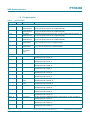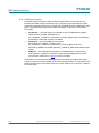
1
PTN3460
eDP to LVDS bridge IC
Rev. 4 — 12 March 2014
Product data sheet
1. General description
PTN3460 is an (embedded) DisplayPort to LVDS bridge device that enables connectivity
between an (embedded) DisplayPort (eDP) source and LVDS display panel. It processes
the incoming DisplayPort (DP) stream, performs DP to LVDS protocol conversion and
transmits processed stream in LVDS format.
PTN3460 has two high-speed ports: Receive port facing DP Source (for example,
CPU/GPU/chip set), Transmit port facing the LVDS receiver (for example., LVDS display
panel controller). The PTN3460 can receive DP stream at link rate 1.62 Gbit/s or
2.7 Gbit/s and it can support 1-lane or 2-lane DP operation. It interacts with DP source via
DP Auxiliary (AUX) channel transactions for DP link training and setup.
It supports single bus or dual bus LVDS signaling with color depths of 18 bits per pixel or
24 bits per pixel and pixel clock frequency up to 112 MHz. The LVDS data packing can be
done either in VESA or JEIDA format. Also, the DP AUX interface transports
I2C-over-AUX commands and support EDID-DDC communication with LVDS panel. To
support panels without EDID ROM, the PTN3460 can emulate EDID ROM behavior
avoiding specific changes in system video BIOS.
PTN3460 provides high flexibility to optimally fit under different platform environments. It
supports three configuration options: multi-level configuration pins, DP AUX interface, and
I2C-bus interface.
PTN3460 can be powered by either 3.3 V supply only or dual supplies (3.3 V/1.8 V) and is
available in the HVQFN56 7 mm 7 mm package with 0.4 mm pitch.
2. Features and benefits
2.1 Device features
Embedded microcontroller and on-chip Non-Volatile Memory (NVM) allow for flexibility
in firmware updates
LVDS panel power-up (/down) sequencing control
Firmware controlled panel power-up (/down) sequence timing parameters
No external timing reference needed
EDID ROM emulation to support panels with no EDID ROM
Supports EDID structure v1.3
On-chip EDID emulation up to seven different EDID data structures
eDP complying PWM signal generation or PWM signal pass through from eDP source
PTN3460
NXP Semiconductors
eDP to LVDS bridge IC
2.2 DisplayPort receiver features
Compliant to DP v1.2 and v1.1a
Compliant to eDP v1.2 and v1.1
Supports Main Link operation with 1 or 2 lanes (default mode is 2-lane operation)
Supports Main Link rate: Reduced Bit Rate (1.62 Gbit/s) and High Bit Rate (2.7 Gbit/s)
Supports 1 Mbit/s AUX channel
Supports Native AUX and I2C-over-AUX transactions
Supports down spreading to minimize EMI
Integrated 50 termination resistors provide impedance matching on both Main Link
lanes and AUX channel
High performance Auto Receive Equalization enabling optimal channel compensation,
device placement flexibility and power saving at CPU/GPU
Supports eDP authentication options: Alternate Scrambler Seed Reset (ASSR) and
Alternate Framing
Supports Fast Link training and Full Link training
Supports DisplayPort symbol error rate measurements
2.3 LVDS transmitter features
Compatible with ANSI/TIA/EIA-644-A-2001 standard
Supports RGB data packing as per JEIDA and VESA data formats
Supports pixel clock frequency from 25 MHz to 112 MHz
Supports single LVDS bus operation up to 112 mega pixels per second
Supports dual LVDS bus operation up to 224 mega pixels per second
Supports color depth options: 18 bpp, 24 bpp
Programmable center spreading of pixel clock frequency to minimize EMI
Supports 1920 1200 at 60 Hz resolution in dual LVDS bus mode
Programmable LVDS signal swing to pre-compensate for channel attenuation or allow
for power saving
Supports PCB routing flexibility by programming for:
LVDS bus swapping
Channel swapping
Differential signal pair swapping
Supports Data Enable polarity programming
DDC control for EDID ROM access – I2C-bus interface up to 400 kbit/s
2.4 Control and system features
Device programmability
Multi-level configuration pins enabling wider choice
I2C-bus slave interface supporting Standard-mode (100 kbit/s) and
Fast-mode (400 kbit/s)
Power management
Low-power state: DP AUX command-based Low-power mode (SET POWER)
Deep power-saving state via a dedicated pin
PTN3460
Product data sheet
All information provided in this document is subject to legal disclaimers.
Rev. 4 — 12 March 2014
© NXP Semiconductors N.V. 2014. All rights reserved.
2 of 32
PTN3460
NXP Semiconductors
eDP to LVDS bridge IC
2.5 General
Power supply: with on-chip regulator
3.3 V 10 % (integrated regulator switched on)
3.3 V 10 %, 1.8 V 5 % (integrated regulator switched off)
ESD: 8 kV HBM, 1 kV CDM
Operating temperature range: 0 C to 70 C
HVQFN56 package 7 mm 7 mm, 0.4 mm pitch; exposed center pad for thermal relief
and electrical ground
3. Applications
AIO platforms
Notebook platforms
Netbooks/net tops
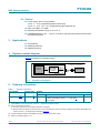
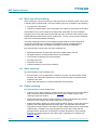
4. System context diagram
Figure 1 illustrates the PTN3460 usage.
notebook or AIO platform
eDP
CPU/GPU/
CHIP SET
PTN3460
DP to LVDS
BRIDGE
LVDS
LVDS PANEL
cable
MOTHERBOARD
002aaf831
Fig 1.
PTN3460 context diagram
5. Ordering information
Table 1.
Ordering information
Type number
Topside mark
PTN3460BS/Fx[1][2]
PTN3460BS[3]
Package
Name
Description
Version
HVQFN56
plastic thermal enhanced very thin quad flat package;
no leads; 56 terminals; body 7 7 0.85 mm[4];
0.4 mm pitch
SOT949-2
[1]
PTN3460BS/Fx is firmware-specific, where the ‘x’ indicates the firmware version.
[2]
Notes on firmware and marking:
a) Firmware versions are not necessarily backwards compatible.
b) Box/reel labels will indicate the firmware version via the orderable part number (for example, labeling will indicate PTN3460BS/F1 for
firmware version 1). A sample label is illustrated in Figure 8.
[3]
Topside marking is limited to PTN3460BS and will not indicate the firmware version.
[4]
Maximum package height is 1 mm.
PTN3460
Product data sheet
All information provided in this document is subject to legal disclaimers.
Rev. 4 — 12 March 2014
© NXP Semiconductors N.V. 2014. All rights reserved.
3 of 32
xxxx xxxxxxxxxxxxxxxxxxxxxxxxxxxxxx x xxxxxxxxxxxxxx xxxxxxxxxx xxx xxxxxx xxxxxxxxxxxxxxxxxxxxxxx xxxxxxxxxxxxxxxxxxxxxx
xxxxx xxxxxx xx xxxxxxxxxxxxxxxxxxxxxxxxxxxxx xxxxxxxxxxxxxxxxxxxxxx xxxxxxxxxxx xxxxxxx xxxxxxxxxxxxxxxxxxx
xxxxxxxxxxxxxxxx xxxxxxxxxxxxxx xxxxxx xx xxxxxxxxxxxxxxxxxxxxxxxxxxxxxxxx xxxxxxxxxxxxxxxxxxxxxxxx xxxxxxx
xxxxxxxxxxxxxxxxxxxxxxxxxxxxxxxxxxxxxxxxxxxxxx xxxxxxxxxxx xxxxx x x
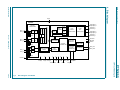
PTN3460
DP1_P,
DP1_N
DIFF CDR,
RCV S2P
10b/8b
Vbias
INTERFACE DE-SKEWING
10b/8b
DIFF CDR,
RCV S2P
G[7:0]
MAIN
STREAM
B[7:0]
TIME
CONV.
TIMING RECOVERY
LVDS
DIGITAL
SUBSYSTEM
LVDS
PHY
SUBSYSTEM
H, V
sync
LVSCKE_P,
LVSCKE_N
LVS[A:D]O_P,
LVS[A:D]O_N
LVSCKO_P,
LVSCKO_N
PVCCEN
NONVOLATILE
MEMORY
DPCD
REGISTERS
SYSTEM
CONTROLLER
Vbias
I2C-BUS
CONTOL
INTERFACE
RCV
AUX_P,
AUX_N
LVS[A:D]E_P,
LVS[A:D]E_N
ISOCHRONOUS LINK
R[7:0]
DE-SCRAM
Rev. 4 — 12 March 2014
All information provided in this document is subject to legal disclaimers.
DP0_P,
DP0_N
RX PHY DIGITAL
DE-SCRAM
RX PHY
ANALOG
SUBSYSTEM
NXP Semiconductors
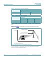
6. Block diagram
PTN3460
Product data sheet
supply
MANCHESTER
CODEC
AUX
CONTROL
BKLTEN
PWMO
EDID
EMULATION
DDC_SCL
DDC
INTERFACE
DDC_SDA
DRV
Vbias
HPDRX
002aaf832
PD_N RST_N
CFG1
TESTMODE
Block diagram of PTN3460
CFG2
DEV_CFG
CFG4
MS_SDA
MS_SCL
PTN3460
Fig 2.
CFG3
eDP to LVDS bridge IC
4 of 32
© NXP Semiconductors N.V. 2014. All rights reserved.
EPS_N
PTN3460
NXP Semiconductors
eDP to LVDS bridge IC
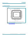
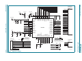
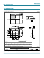
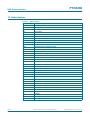
7. Pinning information
43 LVSDO_P
44 LVSDO_N
45 VDD(1V8)
46 LVSCKO_P
47 LVSCKO_N
48 LVSCO_P
49 LVSCO_N
50 VDD(3V3)
51 LVSBO_P
52 LVSBO_N
53 LVSAO_P
54 LVSAO_N
terminal 1
index area
55 n.c.
56 EPS_N
7.1 Pinning
AUX_N
1
42 LVSAE_N
AUX_P
2
41 LVSAE_P
GND
3
40 LVSBE_N
DP0_P
4
39 LVSBE_P
DP0_N
5
38 VDD(3V3)
VDD(1V8)
6
37 LVSCE_N
DP1_P
7
DP1_N
8
35 LVSCKE_N
RST_N
9
34 LVSCKE_P
36 LVSCE_P
PTN3460BS
PD_N 10
33 PVCCEN
HPDRX 11
32 LVSDE_N
DEV_CFG 12
31 LVSDE_P
(1)
PWMO 28
CFG4 27
BKLTEN 26
MS_SCL 25
MS_SDA 24
CFG3 23
CFG2 22
CFG1 21
TESTMODE 20
VDD(1V8) 19
GNDREG 18
GNDREG 17
29 DDC_SCL
n.c. 16
30 DDC_SDA
VDD(3V3) 14
n.c. 15
VDD(3V3) 13
002aaf833
Transparent top view
(1) Center pad is connected to PCB ground plane for electrical grounding and thermal relief.
Fig 3.
Pin configuration for HVQFN56
Refer to Section 13 “Package outline” for package and pin dimensions.
PTN3460
Product data sheet
All information provided in this document is subject to legal disclaimers.
Rev. 4 — 12 March 2014
© NXP Semiconductors N.V. 2014. All rights reserved.
5 of 32
PTN3460
NXP Semiconductors
eDP to LVDS bridge IC
7.2 Pin description
Table 2.
Pin description
Symbol
Pin
Type
Description
DisplayPort interface signals
DP0_P
4
self-biasing
differential input
Differential signal from DP source. DP0_P makes a differential pair with DP0_N.
The input to this pin must be AC-coupled externally.
DP0_N
5
self-biasing
differential input
Differential signal from DP source. DP0_N makes a differential pair with DP0_P.
The input to this pin must be AC-coupled externally.
DP1_P
7
self-biasing
differential input
Differential signal from DP source. DP1_P makes a differential pair with DP1_N.
The input to this pin must be AC-coupled externally.
DP1_N
8
self-biasing
differential input
Differential signal from DP source. DP1_N makes a differential pair with DP1_P.
The input to this pin must be AC-coupled externally.
AUX_P
2
self-biasing
differential I/O
Differential signal towards DP source. AUX_P makes a differential pair with
AUX_N. The pin must be AC-coupled externally.
AUX_N
1
self-biasing
differential I/O
Differential signal towards DP source. AUX_N makes a differential pair with
AUX_P. The pin must be AC-coupled externally.
HPDRX
11
single-ended
3.3 V CMOS
output
Hot Plug Detect signal to DP source.
LVDS interface signals
LVSAE_P
41
LVDS output
Even bus, Channel A differential signal to LVDS receiver. LVSAE_P makes a
differential pair with LVSAE_N.
LVSAE_N
42
LVDS output
Even bus, Channel A differential signal to LVDS receiver. LVSAE_N makes a
differential pair with LVSAE_P.
LVSBE_P
39
LVDS output
Even bus, Channel B differential signal to LVDS receiver. LVSBE_P makes a
differential pair with LVSBE_N.
LVSBE_N
40
LVDS output
Even bus, Channel B differential signal to LVDS receiver. LVSBE_N makes a
differential pair with LVSBE_P.
LVSCE_P
36
LVDS output
Even bus, Channel C differential signal to LVDS receiver. LVSCE_P makes a
differential pair with LVSCE_N.
LVSCE_N
37
LVDS output
Even bus, Channel C differential signal to LVDS receiver. LVSCE_N makes a
differential pair with LVSCE_P.
LVSCKE_P
34
LVDS clock
output
Even bus, clock differential signal to LVDS receiver. LVSCKE_P makes a
differential pair with LVSCKE_N.
LVSCKE_N
35
LVDS clock
output
Even bus, clock differential signal to LVDS receiver. LVSCKE_N makes a
differential pair with LVSCKE_P.
LVSDE_P
31
LVDS output
Even bus, Channel D differential signal to LVDS receiver. LVSDE_P makes a
differential pair with LVSDE_N.
LVSDE_N
32
LVDS output
Even bus, Channel D differential signal to LVDS receiver. LVSDE_N makes a
differential pair with LVSDE_P.
LVSAO_P
53
LVDS output
Odd bus, Channel A differential signal to LVDS receiver. LVSAO_P makes a
differential pair with LVSAO_N.
LVSAO_N
54
LVDS output
Odd bus, Channel A differential signal to LVDS receiver. LVSAO_N makes a
differential pair with LVSAO_P.
LVSBO_P
51
LVDS output
Odd bus, Channel B differential signal to LVDS receiver. LVSBO_P makes a
differential pair with LVSBO_N.
LVSBO_N
52
LVDS output
Odd bus, Channel B differential signal to LVDS receiver. LVSBO_N makes a
differential pair with LVSBO_P.
PTN3460
Product data sheet
All information provided in this document is subject to legal disclaimers.
Rev. 4 — 12 March 2014
© NXP Semiconductors N.V. 2014. All rights reserved.
6 of 32
PTN3460
NXP Semiconductors
eDP to LVDS bridge IC
Table 2.
Pin description …continued
Symbol
Pin
Type
Description
LVSCO_P
48
LVDS output
Odd bus, Channel C differential signal to LVDS receiver. LVSCO_P makes a
differential pair with LVSCO_N.
LVSCO_N
49
LVDS output
Odd bus, Channel C differential signal to LVDS receiver. LVSCO_N makes a
differential pair with LVSCO_P.
LVSCKO_P
46
LVDS clock
output
Odd bus, clock differential signal to LVDS receiver. LVSCKO_P makes a
differential pair with LVSCKO_N.
LVSCKO_N
47
LVDS clock
output
Odd bus, clock differential signal to LVDS receiver. LVSCKO_N makes a
differential pair with LVSCKO_P.
LVSDO_P
43
LVDS output
Odd bus, Channel D differential signal to LVDS receiver. LVSDO_P makes a
differential pair with LVSDO_N.
LVSDO_N
44
LVDS output
Odd bus, Channel D differential signal to LVDS receiver. LVSDO_N makes a
differential pair with LVSDO_P.
DDC_SDA
30
open-drain
DDC data I/O
DDC data signal connection to display panel. Pulled-up by external termination
resistor (5 V tolerant).
DDC_SCL
29
open-drain
DDC clock I/O
DDC clock signal connection to display panel. Pulled-up by external termination
resistor (5 V tolerant).
Panel and backlight interface signals
PVCCEN
33
CMOS output
Panel power (VCC) enable output.
PWMO
28
CMOS output
PWM output signal to display panel.
BKLTEN
26
CMOS output
Backlight enable output.
Control interface signals
PD_N
10
CMOS input
Chip power-down input (active LOW). If PD_N is LOW, then the device is in
Deep power-down completely, even if supply rail is ON; for the device to be able
to operate, the PD_N pin must be HIGH.
RST_N
9
CMOS input
Chip reset pin (active LOW); internally pulled-up. The pin is meant to reset the
device and all its internal states/logic; all internal registers are taken to default
value after RST_N is applied and made HIGH.
If RST_N is LOW, the device stays in reset condition and for the device to be
able to operate, RST_N must be HIGH.
CMOS I/O
I2C-bus address/mode selection pin.
TESTMODE 20
CMOS input
If TESTMODE is left open or pulled HIGH, CFG[4:1] operate as JTAG pins. If
TESTMODE is pulled LOW, these pins serve as configuration pins.
CFG1
input
Behavior defined by TESTMODE pin.
DEV_CFG
12
21
If TESTMODE is left open or pulled HIGH, this pin functions as JTAG TEST
CLOCK input. If TESTMODE is pulled LOW, this pin acts as configuration input.
CFG2
22
input
Behavior defined by TESTMODE pin.
If TESTMODE is left open or pulled HIGH, this pin functions as JTAG MODE
SELECT input. If TESTMODE is pulled LOW, this pin acts as configuration
input.
CFG3
23
input
Behavior defined by TESTMODE pin.
If TESTMODE is left open or pulled HIGH, this pin functions as JTAG TEST
DATA INPUT. If TESTMODE is pulled LOW, this pin acts as configuration input.
CFG4
27
I/O
Behavior defined by TESTMODE pin value.
If TESTMODE is left open or pulled HIGH, this pin functions as JTAG TEST
DATA OUTPUT. If TESTMODE is pulled LOW, this pin acts as configuration
input.
PTN3460
Product data sheet
All information provided in this document is subject to legal disclaimers.
Rev. 4 — 12 March 2014
© NXP Semiconductors N.V. 2014. All rights reserved.
7 of 32
PTN3460
NXP Semiconductors
eDP to LVDS bridge IC
Table 2.
Pin description …continued
Symbol
Pin
Type
Description
MS_SDA
24
open-drain (I2C)
data input/output
I2C-bus data signal connection to I2C-bus master or slave. Pulled up by external
resistor.
MS_SCL
25
I2C-bus clock signal connection to I2C-bus master or slave. Pulled up by
open-drain (I2C)
clock input/output external resistor.
n.c.
55
-
not connected; reserved.
EPS_N
56
input
Can be left open or pulled HIGH for 3.3 V supply only option relying on internal
regulator for 1.8 V generation.
Should be pulled down to GND for dual supply (3.3 V/1.8 V) option.
Supply, ground and decoupling
VDD(3V3)
13, 14, power
38, 50
3.3 V supply input.
VDD(1V8)
6, 45
power
1.8 V supply input.
VDD(1V8)
19
power
1.8 V regulator supply output.
n.c.
15, 16
power
Not connected.
GND
3
power
Ground.
GNDREG
17, 18
power
Ground for regulator.
GND
center
pad
power
The center pad must be connected to motherboard GND plane for both
electrical ground and thermal relief.
8. Functional description
PTN3460 is an (Embedded) DisplayPort to LVDS bridge IC that processes the incoming
DisplayPort (DP) stream, performs DP to LVDS protocol conversion and transmits
processed stream in LVDS format. Refer to Figure 2 “Block diagram of PTN3460”.
The PTN3460 consists of:
• DisplayPort receiver
• LVDS transmitter
• System control and operation
The following sections describe individual sub-systems and their capabilities in more
detail.
8.1 DisplayPort receiver
PTN3460 implements a DisplayPort receiver consisting of 2-lane Main Link and AUX
channel.
With its advanced signal processing capability, it can handle Fast Link training or Full Link
training scheme. PTN3460 implements a high-performance Auto Receive Equalizer and
Clock Data Recovery (CDR) algorithm, with which it identifies and selects an optimal
operational setting for given channel environment. Given that the device is targeted
primarily for embedded Display connectivity, both Display Authentication and Copy
Protection Method 3a (Alternate Scrambler Seed Reset) and Method 3b (Enhanced
Framing) are supported, as per eDP 1.2.
PTN3460
Product data sheet
All information provided in this document is subject to legal disclaimers.
Rev. 4 — 12 March 2014
© NXP Semiconductors N.V. 2014. All rights reserved.
8 of 32
PTN3460
NXP Semiconductors
eDP to LVDS bridge IC
The PTN3460 DPCD registers can be accessed by DP source through AUX channel. It
supports both Native AUX transactions and I2C-over-AUX transactions.
Native AUX transactions are used to access PTN3460 DisplayPort Configuration Data
(DPCD) registers (e.g., to facilitate Link training, check error conditions, etc.) and
I2C-over-AUX transactions are used to perform any required access to DDC bus
(e.g., EDID reads).
Given that the HPDRX pin is internally connected to GND through an integrated pull-down
resistor (> 100 k), the DP source will see HPDRX pin as LOW indicating that the
DisplayPort receiver is not ready when the device is not powered. This helps avoid raising
false events to the source. After power-up, PTN3460 continues to drive HPDRX pin LOW
until completion of internal initialization. After this, PTN3460 generates HPD signal to
notify DP source and take corrective action(s).
8.1.1 DP Link
PTN3460 is capable of operating either in DP 2-lane or 1-lane mode. The default is 2-lane
mode of operation (in alignment with PTN3460 DCPD register 00002h,
MAX_LANE_COUNT = 2).
There are two ways to enable 1-lane operation in an application:
• Connect both DP lanes of PTN3460 to the DP source. This enables the DP source to
decide/use only required number of lanes based on display resolution.
• Connect only 1 lane (DP0_P, DP0_N) to DP source and modify the DPCD register
00002h, MAX_LANE_COUNT to ‘1’ through NXP I2C configuration utility to modify the
internal configuration table. Please consult NXP for more details regarding the
Flash-over-AUX and DOS utilities.
8.1.2 DPCD registers
DPCD registers are described in VESA DisplayPort v1.1a/1.2 specifications in detail and
PTN3460 supports DPCD version 1.2.
PTN3460 configuration registers can be accessed through DP AUX channel from the
GPU/CPU, if required. They are defined under vendor-specific region starting at base
address 0x00510h. So any configuration register can be accessed at DPCD address
obtained by adding the register offset and base address.
PTN3460 supports down spreading on DP link and this is reflected in DPCD register
MAX_DOWNSPREAD at address 0003h. Further, the DP source could control
down spreading and inform PTN3460 via DOWNSPREAD_CTRL register at DPCD
register 00107h.
The key aspect is that the system designer must take care that the Input video payload fits
well within both DP link bandwidth and LVDS bandwidth (for a given pixel frequency,
SSC depths) when clock spreading is enabled. Also, another aspect for the system
designer is to ensure LVDS (panel) TCONs are capable of handling SSC modulated LVDS
signaling.
PTN3460
Product data sheet
All information provided in this document is subject to legal disclaimers.
Rev. 4 — 12 March 2014
© NXP Semiconductors N.V. 2014. All rights reserved.
9 of 32
PTN3460
NXP Semiconductors
eDP to LVDS bridge IC
8.2 LVDS transmitter
The LVDS interface can operate either in Single or Dual LVDS Bus mode at pixel clock
frequencies over the range of 25 MHz to 112 MHz and color depths of 18 bpp or 24 bpp.
Each LVDS bus consists of 3/4 differential data pairs and one clock pair. PTN3460 can
packetize RGB video data, HSYNC, VSYNC, DE either in VESA or JEIDA format. To
enable system EMI reduction, the device can be programmed for center spreading of
LVDS channel clock outputs.
The LVDS interface can be flexibly configured using multi-level configuration pins (CFG1,
CFG2, CFG3, CFG4) or via register interface. The configuration pins and the
corresponding definitions are described in Table 3 through Table 6. Nevertheless, as the
configuration pins are designed for general purpose, their definitions can be modified and
they can be used for any other purposes. However, this can be achieved through firmware
upgrade only.
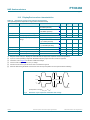
Table 3.
CFG1 configuration options
Configuration input setting
Number of LVDS links
LOW
single LVDS bus
HIGH
dual LVDS bus
Table 4.
CFG2 configuration options
3-level configuration input setting
Data format
Number of bits per pixel (bpp)
LOW
VESA
24 bpp
open
JEIDA
24 bpp
HIGH
JEIDA or VESA
18 bpp
Table 5.
CFG3 configuration options[1]
3-level configuration input setting
LVDS clock frequency spread depth control
LOW
0%
open
1%
HIGH
0.5 %
[1]
LVDS center spreading modulation frequency is kept at 32.9 kHz.
Table 6.
CFG4 configuration options
3-level configuration input setting
pull-down
Product data sheet
to GND
LVDS output swing (typical value)
250 mV
open
300 mV
pull-up resistor[1] to VDD(3V3)
400 mV
[1]
PTN3460
resistor[1]
Pull-up/down resistor value in the range of 1 k to 10 k.
All information provided in this document is subject to legal disclaimers.
Rev. 4 — 12 March 2014
© NXP Semiconductors N.V. 2014. All rights reserved.
10 of 32
PTN3460
NXP Semiconductors
eDP to LVDS bridge IC
The VESA and JEIDA data format definitions are described in Table 7 to Table Table 13.
Table 7.
LVDS single bus, 18 bpp, VESA or JEIDA data packing
Channel
Bit position
6
5
4
3
2
1
0
LVDS odd differential channel A
bit 0
bit 5
bit 4
bit 3
bit 2
bit 1
bit 0
LVDS odd differential channel B
bit 1
bit 0
bit 5
bit 4
bit 3
bit 2
bit 1
LVDS odd differential channel C
DE
VSYNC
HSYNC
bit 5
bit 4
bit 3
bit 2
Table 8.
LVDS single bus, 24 bpp, VESA data packing
Channel
Bit position
6
5
4
3
2
1
0
LVDS odd differential channel A
bit 0
bit 5
bit 4
bit 3
bit 2
bit 1
bit 0
LVDS odd differential channel B
bit 1
bit 0
bit 5
bit 4
bit 3
bit 2
bit 1
bit 4
bit 3
bit 2
bit 6
bit 7
bit 6
LVDS odd differential channel C
DE
VSYNC
HSYNC
bit 5
LVDS odd differential channel D
don’t care
bit 7
bit 6
bit 7
Table 9.
LVDS dual bus, 18 bpp, VESA data packing
Channel
Bit position
6
5
4
3
2
1
0
LVDS odd differential channel A
bit 0
bit 5
bit 4
bit 3
bit 2
bit 1
bit 0
LVDS odd differential channel B
bit 1
bit 0
bit 5
bit 4
bit 3
bit 2
bit 1
LVDS odd differential channel C
DE
VSYNC
HSYNC
bit 5
bit 4
bit 3
bit 2
LVDS even differential channel A
bit 0
bit 5
bit 4
bit 3
bit 2
bit 1
bit 0
LVDS even differential channel B
bit 1
bit 0
bit 5
bit 4
bit 3
bit 2
bit 1
LVDS even differential channel C
DE
VSYNC
HSYNC
bit 5
bit 4
bit 3
bit 2
Table 10.
LVDS dual bus, 24 bpp, VESA data packing
Channel
Bit position
6
5
4
3
2
1
0
LVDS odd differential channel A
bit 0
bit 5
bit 4
bit 3
bit 2
bit 1
bit 0
LVDS odd differential channel B
bit 1
bit 0
bit 5
bit 4
bit 3
bit 2
bit 1
bit 4
bit 3
bit 2
LVDS odd differential channel C
DE
VSYNC
HSYNC
bit 5
LVDS odd differential channel D
don’t care
bit 7
bit 6
bit 7
bit 6
bit 7
bit 6
LVDS even differential channel A
bit 0
bit 5
bit 4
bit 3
bit 2
bit 1
bit 0
LVDS even differential channel B
bit 1
bit 0
bit 5
bit 4
bit 3
bit 2
bit 1
bit 4
bit 3
bit 2
bit 6
bit 7
bit 6
LVDS even differential channel C
DE
VSYNC
HSYNC
bit 5
LVDS even differential channel D
don’t care
bit 7
bit 6
bit 7
PTN3460
Product data sheet
All information provided in this document is subject to legal disclaimers.
Rev. 4 — 12 March 2014
© NXP Semiconductors N.V. 2014. All rights reserved.
11 of 32
PTN3460
NXP Semiconductors
eDP to LVDS bridge IC
Table 11.
LVDS single bus, 24 bpp, JEIDA data packing
Channel
Bit position
6
5
4
3
2
1
0
LVDS odd differential channel A
bit 2
bit 7
bit 6
bit 5
bit 4
bit 3
bit 2
LVDS odd differential channel B
bit 3
bit 2
bit 7
bit 6
bit 5
bit 4
bit 3
LVDS odd differential channel C
DE
VSYNC
HSYNC
bit 7
bit 6
bit 5
bit 4
LVDS odd differential channel D
don’t care
bit 1
bit 0
bit 1
bit 0
bit 1
bit 0
Table 12.
LVDS dual bus, 18 bpp, JEIDA data packing
Channel
Bit position
6
5
4
3
2
1
0
LVDS odd differential channel A
bit 0
bit 5
bit 4
bit 3
bit 2
bit 1
bit 0
LVDS odd differential channel B
bit 1
bit 0
bit 5
bit 4
bit 3
bit 2
bit 1
LVDS odd differential channel C
DE
VSYNC
HSYNC
bit 5
bit 4
bit 3
bit 2
LVDS even differential channel A
bit 0
bit 5
bit 4
bit 3
bit 2
bit 1
bit 0
LVDS even differential channel B
bit 1
bit 0
bit 5
bit 4
bit 3
bit 2
bit 1
LVDS even differential channel C
DE
VSYNC
HSYNC
bit 5
bit 4
bit 3
bit 2
Table 13.
LVDS dual bus, 24 bpp, JEIDA data packing
Channel
Bit position
6
5
4
3
2
1
0
LVDS odd differential channel A
bit 2
bit 7
bit 6
bit 5
bit 4
bit 3
bit 2
LVDS odd differential channel B
bit 3
bit 2
bit 7
bit 6
bit 5
bit 4
bit 3
LVDS odd differential channel C
DE
VSYNC
HSYNC
bit 7
bit 6
bit 5
bit 4
LVDS odd differential channel D
don’t care
bit 1
bit 0
bit 1
bit 0
bit 1
bit 0
LVDS even differential channel A
bit 2
bit 7
bit 6
bit 5
bit 4
bit 3
bit 2
LVDS even differential channel B
bit 3
bit 2
bit 7
bit 6
bit 5
bit 4
bit 3
LVDS even differential channel C
DE
VSYNC
HSYNC
bit 7
bit 6
bit 5
bit 4
LVDS even differential channel D
don’t care
bit 1
bit 0
bit 1
bit 0
bit 1
bit 0
PTN3460 delivers great flexibility by supporting more programmable options via I2C-bus
or AUX interface. Please refer to Section 8.3.8 for more details.
PTN3460
Product data sheet
All information provided in this document is subject to legal disclaimers.
Rev. 4 — 12 March 2014
© NXP Semiconductors N.V. 2014. All rights reserved.
12 of 32
PTN3460
NXP Semiconductors
eDP to LVDS bridge IC
8.3 System control and operation
With its combination of embedded microcontroller, non-volatile memory, DPCD AUX and
I2C-bus interfaces, PTN3460 delivers significant value for customer applications by
providing higher degree of control and programmability.
By default, all user controllable registers can be accessed through DPCD AUX interface.
This interface is always enabled. This AUX interface delivers seamless access of
PTN3460 registers to system/platform (GPU) firmware driver. Nevertheless, use of
I2C-bus interface for configuring PTN3460 is left to the choice of system integrator.
DEV_CFG (pin 12) sets up I2C-bus configuration mode:
• Pull-down resistor to GND — PTN3460 operates as I2C-bus slave, low address
(0x40h)
• Open — PTN3460 operates as I2C-bus slave, high address (0xC0h)
• Pull-up resistor to VDD(3V3) — PTN3460 operates as I2C-bus master capable of
reading from external EEPROM
8.3.1 Reset, power-down and power-on initialization
The device has a built-in reset circuitry that generates internal reset signal after power-on.
All the internal registers and state machines are initialized and the registers take default
values. In addition, PTN3460 has a dedicated control pin RST_N. This serves the same
purpose as power-on reset, but without power cycling of the device/platform.
PTN3460 starts up in a default condition after power-on or after RST_N is toggled from
LOW to HIGH. The configuration pins are sampled at power-on, or external reset, or when
returning from Deep Sleep.
PTN3460 goes into Deep power-saving when PD_N is LOW. This will trigger a
power-down sequence. To leave Deep power-saving state, the system needs to drive
PD_N back to HIGH. If PD_N pin is open, the device will not enter Deep power-saving
state. Once the device is in Deep power-saving condition, the HPDRX pin will go LOW
automatically and this can be used by the system to remove the 3.3 V supply, if required.
Remark: The device will not respect the Panel power-down sequence if PD_N is asserted
LOW while video is being streamed to the display. So the system is not supposed to
toggle PD_N and RST_N pins asynchronously while the LVDS output is streaming video
to the display panel, but instead follow the panel powering sequence as described in
Section 8.3.3.
PTN3460
Product data sheet
All information provided in this document is subject to legal disclaimers.
Rev. 4 — 12 March 2014
© NXP Semiconductors N.V. 2014. All rights reserved.
13 of 32
PTN3460
NXP Semiconductors
eDP to LVDS bridge IC
8.3.2 LVDS panel control
PTN3460 implements eDPv1.2 specific DPCD registers that concern panel power,
backlight and PWM controls and the DP source can issue AUX commands to initiate
panel power-up/down sequence as required. Also, PTN3460 supports LVDS panel control
pins — backlight enable, panel power enable and PWM — that can be set via AUX
commands.
• PVCCEN pin — the signal output is set based on SET_POWER DPCD register
00600h and SET_POWER_CAPABLE bit of
EDP_GENERAL_CAPABILITY_REGISTER_1 DPCD register 00701h and detection
and handling of video data stream by PTN3460
• BKLTEN pin — the signal output is set based on
BACKLIGHT_PIN_ENABLE_CAPABLE bit of
EDP_GENERAL_CAPABILITY_REGISTER_1 DPCD register 00701h and
BACKLIGHT_ENABLE bit of EDP_DISPLAY_CONTROL_REGISTER DPCD register
00720h
• PWMO pin — the PWM signal generated by PTN3460 based on controls set in
DPCD registers. In addition, PTN3460 can pass through PWM signal from eDP
source as well. Please refer to Ref. 2 for more information.
All the panel control enable and signal outputs from PTN3460 are aligned with panel
power-on sequence timing including LVDS video output generation. It is important to note
that the Panel power must be delivered by the system platform and it should be gated by
PVCCEN signal.
PTN3460
Product data sheet
All information provided in this document is subject to legal disclaimers.
Rev. 4 — 12 March 2014
© NXP Semiconductors N.V. 2014. All rights reserved.
14 of 32
PTN3460
NXP Semiconductors
eDP to LVDS bridge IC
8.3.3 Panel power sequencing
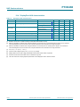
Figure 4 illustrates an example of panel power-up/power-down sequence for PTN3460.
Depending on the source behavior and PTN3460 firmware version, the powering
sequence/timing could have some slight differences.
T12 > 500 ms
VDD(3V3)
LCDVCC
PVCCEN
T2 < 50 ms
LVDS interface
black video
from PTN3460
T5 < 50 ms
video from source
SINK_STATUS
HPDRX
eDP AUX channel
eDP Main Link
display backlight
AUX channel operational
Link Training
idle
valid video data
disabled
enabled
T3 > 200 ms
to 1000 ms
video or IDLE stream
from DP source
T4 > 200 ms
002aaf839
T2: Time interval between panel power enable signal (PVCCEN) going HIGH and video data/clock driven on LVDS interface.
T3: Time interval between valid video data/clock on LVDS interface and backlight enable signal (BKLTEN) going HIGH.
T4: Time interval between backlight enable signal (BKLTEN) made LOW and stopping of video data/clock on LVDS interface.
T5: Time interval between stopping of video data/clock on LVDS interface and panel power enable signal (PVCCEN) made
LOW.
T12: Time interval for which PVCCEN is held LOW before it can be made HIGH.
Fig 4.
Panel power-up/power-down sequence example
When working with eDP capable DP sources, PTN3460 supports the following (for
specific sequence, refer to Figure 4):
• After power-on/startup, HPDRX is asserted HIGH, DP source will start AUX
communication for initialization, perform Link Training and starts the video data
stream. Once presence of video data is detected, PTN3460 will assert PVCCEN to
HIGH, synchronize to video stream, output LVDS data and assert rise the Sink_status
lock as indicated in DPCD register (0x00205h). PTN3460 will wait for Backlight
enabling delay (T3) to avoid visual artifacts and program the BKLTEN HIGH.
• While transitioning out of Active state by receiving DPCD 0x600 to set PTN3460 in
D3 mode, PTN3460 will disable BKLTEN prior to cutting off Video streaming to avoid
visible artifacts following specific panel specifications. PTN3460 will assert PVCCEN
to LOW after T5 delay as long as either if the video stream is stopped or video
synchronization is lost. This is to avoid driving the LVDS panel with illegal stream for
long periods of time. It is good practice for sources to keep video data or at least
DP-idle stream active during T4 + T5.
• When PTN3460 is in Low-power state (DisplayPort D3 power state), the LVDS
differential I/Os are weakly pulled down to 0 V. In this state, PVCCEN and BKLTEN
are pulled LOW.
• When PD_N is LOW, which sets PTN3460 in Deep power-saving state, the BKLTEN
pin is set to LOW. LVDS differential I/Os are pulled LOW via the weak pull-downs.
PTN3460
Product data sheet
All information provided in this document is subject to legal disclaimers.
Rev. 4 — 12 March 2014
© NXP Semiconductors N.V. 2014. All rights reserved.
15 of 32
PTN3460
NXP Semiconductors
eDP to LVDS bridge IC
8.3.4 Termination resistors
The device provides integrated and calibrated 50 termination resistors on both
DisplayPort Main Link lanes and AUX channel.
8.3.5 Reference clock input
PTN3460 does not require an external clock. It relies fully on the clock derived internally
from incoming DP stream or on-chip clock generator.
8.3.6 Power supply
PTN3460 can be flexibly supplied with either 3.3 V supply only or dual supplies
(3.3 V/1.8 V). When supplied with 3.3 V supply only, the integrated regulator is used to
generate 1.8 V for internal circuit operation. In this case, the EPS_N pin must be pulled
HIGH or left open. For optimal power consumption, dual supply option (3.3 V and 1.8 V) is
recommended.
8.3.7 Power management
In tune with the system application needs, PTN3460 implements aggressive techniques to
support system power management and conservation. The device can exist in one of the
three different states as described below:
• Active state when the device is fully operational.
• Low-power state when DP source issues AUX SET_POWER command on DPCD
register 00600h. In this state, AUX and HPD circuits are operational but the main
DP Link and LVDS Bus are put to high-impedance condition. The device will transition
back to Active state when the DP source sets the corresponding DPCD register bits to
‘DisplayPort D0/Normal Operation mode’. The I2C-bus interface will not be
operational in this state.
• Deep power-saving state: In this state PTN3460 is put to ultra low-power condition.
This is effected when PD_N is LOW. To get back to Active state, PD_N must be made
HIGH. The external interfaces (like I2C, AUX, DP, LVDS, configuration pins) will not be
operational.
8.3.8 Register interface — control and programmability
PTN3460 has a register interface that can be accessed by CPU/GPU or System
Controller to choose settings suitably for the System application needs. The registers can
be read/written either via DP AUX or I2C-bus interface. It is left to system integrator choice
to use an interface to configure PTN3460.
PTN3460 provides greater level of configurability of certain parameters (e.g., LVDS output
swing, spreading depth, etc.) via registers beyond what is available through pins. The
register settings override the pin values. All registers must be configured during power-on
initialization after HPDRX is HIGH. The registers and bit definitions are described in
“I2C-bus utility and programming guide for firmware and EDID update” (Ref. 3).
8.3.9 EDID handling
The DP source issues EDID reads using I2C-over-AUX transactions and PTN3460, in
turn, reads from the panel EDID ROM and passes back to the source. To support
seamless functioning of panels without EDID ROM, the PTN3460 can be programmed to
emulate EDID ROM and delivers internally stored EDID information to the source. Given
PTN3460
Product data sheet
All information provided in this document is subject to legal disclaimers.
Rev. 4 — 12 March 2014
© NXP Semiconductors N.V. 2014. All rights reserved.
16 of 32
PTN3460
NXP Semiconductors
eDP to LVDS bridge IC
that EDID is specific to panels, PTN3460 enables system integrator to program EDID
information into embedded memory through DP AUX and I2C-bus interfaces. The
supported EDID ROM emulation size is 896 bytes (seven EDID data structures, each of
128 bytes).
9. Application design-in information
Figure 5 illustrates PTN3460 usage in a system context. The eDP inputs are connected to
DP source port on CPU/GPU and the LVDS outputs are connected to LVDS panel TCON.
PTN3460
Product data sheet
All information provided in this document is subject to legal disclaimers.
Rev. 4 — 12 March 2014
© NXP Semiconductors N.V. 2014. All rights reserved.
17 of 32
xxxxxxxxxxxxxxxxxxxxx xxxxxxxxxxxxxxxxxxxxxxxxxx xxxxxxx x x x xxxxxxxxxxxxxxxxxxxxxxxxxxxxxx xxxxxxxxxxxxxxxxxxx xx xx xxxxx
xxxxxxxxxxxxxxxxxxxxxxxxxxx xxxxxxxxxxxxxxxxxxx xxxxxx xxxxxxxxxxxxxxxxxxxxxxxxxxxxxxxxxxx xxxxxxxxxxxx x x
xxxxxxxxxxxxxxxxxxxxx xxxxxxxxxxxxxxxxxxxxxxxxxxxxxx xxxxx xxxxxxxxxxxxxxxxxxxxxxxxxxxxxxxxxxxxxxxxxxxxxxxxxx xxxxxxxx
xxxxxxxxxxxxxxxxxxxxxxxxx xxxxxxxxxxxxxxxxxxxx xxx
NXP Semiconductors
PTN3460
1
HPD pull-down
is integrated into
R1
silicon (400 kΩ)
100 kΩ
DP_HPD
2 0.1 μF
DP_L1n
DP_LANE1P
C16 1
2 0.1 μF
DP_L1p
DP_LANE0N
C17 1
2 0.1 μF
DP_L0n
DP_LANE0P
C18 1
2 0.1 μF
DP_L0p
AUXP
C19 1
2 0.1 μF
DP_AUXP
AUXN
MS_SCL
MS_SDA
C20 1
2 0.1 μF
DP_AUXN
Application diagram
1V8_REG
C13
4.7 μF
1
1
LVSCE_N
LVSCE_P
LVSCKE_N
LVSCKE_P
PVCCEN
LVSDE_N
LVSDE_P
DDC_SDA
DDC_SCL
LVSDO_N
LVSDO_P
LVSAE_N
LVSAE_P
LVSBE_N
LVSBE_P
LVSCE_N
LVSCE_P
LVSCKE_N
LVSCKE_P
PVCCEN
LVSDE_N
LVSDE_P
DDC_SDA
DDC_SCL
BKLTEN
PWMO
option
DEV_CFG 1 R2 2
10 kΩ
open: I2C-bus slave,
high address (0C0h)
LOW: I2C-bus slave (040h)
+3V3
R3
EPS_N
1
PD_N
10 kΩ
1 R4 2
C12
0.1 μF
2
LVSDO_N
LVSDO_P
56
55
54
53
52
51
50
49
48
47
46
45
44
43
LVSAE_N
LVSAE_P
LVSBE_N
LVSBE_P
option
2
C15 1
C4
0.1 μF
2
configuration
options
CFG1
CFG2
CFG3
CFG4
10 kΩ
TESTMODE 1 R5 2
10 kΩ
002aag619
PTN3460
DP_LANE1N
42
41
40
39
38
37
36
35
34
33
32
31
30
29
C3
0.1 μF
LVSCO_N
LVSCO_P
LVSCKO_N
LVSCKO_P
eDP to LVDS bridge IC
18 of 32
© NXP Semiconductors N.V. 2014. All rights reserved.
Fig 5.
optional
2
eDP port or
PCH port D
DP_HPD
LVSCO_N
LVSCO_P
LVSCKO_N
LVSCKO_P
2
(optional)
GND
C14
1 μF
(25 V)
center pad
1
C11
0.01 μF
TESTMODE
CFG1
CFG2
CFG3
MS_SDA
MS_SCL
BKLTEN
CFG4
PWMO
2
1
1
C9
1 μF
(25 V)
C10
0.01 μF
2
C8
0.47 μF
+3V3_REG
1
2
2
1
1 L3
FB
1
+3V3
PTN3460
2
PD_N
DP_HPD
DEV_CFG
LVSAE_N
LVSAE_P
LVSBE_N
LVSBE_P
VDD(3V3)
LVSCE_N
LVSCE_P
LVSCKE_N
LVSCKE_P
PVCCEN
LVSDE_N
LVSDE_P
DDC_SDA
DDC_SCL
n.c.
n.c.
GNDREG
GNDREG
VDD(1V8)
TESTMODE
CFG1
CFG2
CFG3
MS_SDA
MS_SCL
BKLTEN
CFG4
PWMO
DP_L1p
DP_L1n
AUX_N
AUX_P
GND
DP0_P
DP0_N
VDD(1V8)
DP1_P
DP1_N
RST_N
PD_N
HPDRX
DEV_CFG
VDD(3V3)
VDD(3V3)
15
16
17
18
19
20
21
22
23
24
25
26
27
28
1
2
2
2
1
2
3
4
5
6
7
8
9
10
11
12
13
14
C7
DP_AUXp
0.01 μF
DP_L0p
DP_L0n
2
Rev. 4 — 12 March 2014
All information provided in this document is subject to legal disclaimers.
C6
2.2 μF
1
DP_AUXn
C5
0.1 μF
1
2
EPS_N
n.c.
LVSAO_N
LVSAO_P
LVSBO_N
LVSBO_P
VDD(3V3)
LVSCO_N
LVSCO_P
LVSCKO_N
LVSCKO_P
VDD(1V8)
LVSDO_N
LVSDO_P
U1
1V8_DP
1
1 L2
FB
C2
0.1 μF
2
1V8_REG
1
1
+3V3_IO
EPS_N
1V8_REG
2
C1
2.2 μF
LVSAO_N
LVSAO_P
LVSBO_N
LVBSO_P
+3V3_IO
1 L1
FB
LVSAO_N
LVSAO_P
LVSBO_N
LVBSO_P
2
+3.3 V
2
Product data sheet
LVDS panel
and backlight
inverter
PTN3460
NXP Semiconductors
eDP to LVDS bridge IC
10. Limiting values
Table 14. Limiting values
In accordance with the Absolute Maximum Rating System (IEC 60134).
Symbol
Parameter
VDD
supply voltage
VI
input voltage
Tstg
storage temperature
VESD
Conditions
electrostatic discharge
voltage
Min
Max
Unit
[1]
0.3
+4.6
V
3.3 V CMOS inputs
[1]
0.3
VDD + 0.5 V
65
+150
C
HBM
[2]
-
8000
V
CDM
[3]
-
1000
V
[1]
All voltage values, except differential voltages, are with respect to network ground terminal.
[2]
Human Body Model: ANSI/EOS/ESD-S5.1-1994, standard for ESD sensitivity testing, Human Body Model
– Component level; Electrostatic Discharge Association, Rome, NY, USA.
[3]
Charged-Device Model: ANSI/EOS/ESD-S5.3-1-1999, standard for ESD sensitivity testing,
Charged-Device Model – Component level; Electrostatic Discharge Association, Rome, NY, USA.
11. Recommended operating conditions
Table 15. Operating conditions
Over operating free-air temperature range, unless otherwise noted.
Symbol
Parameter
Min
Typ
Max
Unit
VDD(3V3)
supply voltage (3.3 V)
3.0
3.3
3.6
V
VDD(1V8)
supply voltage (1.8 V)
1.7
1.8
1.9
V
VI
input voltage
3.3 V CMOS inputs
0
3.3
3.6
V
open-drain I/O with
respect to ground
(e.g., DDC_SCL,
DDC_SDA, MS_SDA,
MS_SCL)
0
5
5.5
V
operating in free air
0
-
70
C
Tamb
PTN3460
Product data sheet
Conditions
ambient temperature
All information provided in this document is subject to legal disclaimers.
Rev. 4 — 12 March 2014
© NXP Semiconductors N.V. 2014. All rights reserved.
19 of 32
PTN3460
NXP Semiconductors
eDP to LVDS bridge IC
12. Characteristics
12.1 Device characteristics
Table 16. Device characteristics
Over operating free-air temperature range, unless otherwise noted.
Symbol
Parameter
Conditions
Min
Typ
Max
Unit
tstartup
start-up time
device start-up time from power-on and
RST_N = HIGH; supply voltage within
operating range to specified operating
characteristics
-
-
90
ms
tw(rst)
reset pulse width
device is supplied with valid supply voltage
10
-
-
s
td(rst)
reset delay time[1]
device is supplied with valid supply voltage
-
-
90
ms
td(pwrsave-act)
delay time from
power-save to active
time between PD_N going HIGH and HPD
raised HIGH by PTN3460; RST_N is HIGH.
-
-
90
ms
Device is supplied with valid supply voltage.
[1]
Time for device to be ready after rising edge of RST_N.
12.2 Power consumption
Table 17. Power consumption
At operating free-air temperature of 25 C and under nominal supply value (unless otherwise noted).
Symbol
Pcons
[1]
Parameter
power
consumption
Conditions
Single supply mode
EPS_N = HIGH
or open
Dual supply mode
EPS_N = LOW
Unit
Min
Typ
Max
Min
Typ
Max
Active mode;
1440 900 at 60 Hz;
24 bits per pixel; dual LVDS bus
[1]
-
430
-
-
290
-
mW
Active mode;
1600 900 at 60 Hz;
24 bits per pixel; dual LVDS bus
[1]
-
448
-
-
305
-
mW
Active mode;
1920 1200 at 60 Hz;
24-bits per pixel; dual LVDS bus
[1]
-
570
-
-
380
-
mW
D3 mode/Power-saving mode;
when PTN3460 is set to
Power-saving mode via
‘SET_POWER’ AUX command by
eDP source; AUX and HPDRX
circuitry are only kept active
-
27
-
-
15
-
mW
Deep power-saving/Shutdown mode;
when PD_N is LOW and the device is
supplied with valid supply voltage
-
5
-
-
2
-
mW
For Active mode power consumption, LVDS output swing of 300 mV is considered.
PTN3460
Product data sheet
All information provided in this document is subject to legal disclaimers.
Rev. 4 — 12 March 2014
© NXP Semiconductors N.V. 2014. All rights reserved.
20 of 32
PTN3460
NXP Semiconductors
eDP to LVDS bridge IC
12.3 DisplayPort receiver characteristics
Table 18. DisplayPort receiver main channel characteristics
Over operating free-air temperature range (unless otherwise noted).
Symbol
UI
Parameter
Conditions
unit interval
fDOWN_SPREAD
link clock down spreading
CRX
AC coupling capacitor
VRX_DIFFp-p
differential input peak-to-peak
voltage
Min
Typ
Max
Unit
high bit rate
(2.7 Gbit/s per lane)
[1]
-
370
-
ps
reduced bit rate
(1.62 Gbit/s per lane)
[1]
-
617
-
ps
[2]
0
-
0.5
%
75
-
200
nF
at receiver package pins
high bit rate
(2.7 Gbit/s per lane)
[3]
120
-
-
mV
reduced bit rate
(1.62 Gbit/s per lane)
[3]
40
-
-
mV
RX DC common mode voltage
[4]
0
-
2.0
V
RX short-circuit current limit
[5]
-
-
50
mA
fRX_TRACKING_BW
jitter tracking bandwidth
[6]
Geq(max)
maximum equalization gain
VRX_DC_CM
IRX_SHORT
at 1.35 GHz
20
-
-
MHz
-
15
-
dB
[1]
Range is nominal 350 ppm. DisplayPort channel RX does not require local crystal for channel clock generation.
[2]
Up to 0.5 % down spreading is supported. Modulation frequency range of 30 kHz to 33 kHz is supported.
[3]
Informative; refer to Figure 6 for definition of differential voltage.
[4]
Common-mode voltage is equal to Vbias_RX voltage.
[5]
Total drive current of the input bias circuit when it is shorted to its ground.
[6]
Minimum CDR tracking bandwidth at the receiver when the input is repetition of D10.2 symbols without scrambling.
VD+
VDIFF_PRE
VCM
VDIFF
VD−
002aaf363
pre-emphasis = 20Log(VDIFF_PRE / VDIFF)
Fig 6.
PTN3460
Product data sheet
Definition of pre-emphasis and differential voltage
All information provided in this document is subject to legal disclaimers.
Rev. 4 — 12 March 2014
© NXP Semiconductors N.V. 2014. All rights reserved.
21 of 32
PTN3460
NXP Semiconductors
eDP to LVDS bridge IC
12.4 DisplayPort AUX characteristics
Table 19.
DisplayPort AUX characteristics
Symbol
UI
tjit(cc)
VAUX_DIFFp-p
Parameter
Conditions
Min
Typ
Max
Unit
unit interval
[1]
0.4
0.5
0.6
s
cycle-to-cycle jitter time
transmitting device
[2]
-
-
0.04
UI
receiving device
[3]
-
-
0.05
UI
transmitting device
[4]
0.39
-
1.38
V
receiving device
[4]
0.32
-
1.36
V
AUX differential peak-to-peak voltage
RAUX_TERM(DC) AUX CH termination DC resistance
VAUX_DC_CM
informative
-
100
-
[5]
0
-
2.0
V
[6]
-
-
0.3
V
AUX short-circuit current limit
[7]
-
-
90
mA
AUX AC coupling capacitor
[8]
75
-
200
nF
AUX DC common-mode voltage
VAUX_TURN_CM AUX turnaround common-mode voltage
IAUX_SHORT
CAUX
[1]
Results in the bit rate of 1 Mbit/s including the overhead of Manchester II coding.
[2]
Maximum allowable UI variation within a single transaction at connector pins of a transmitting device. Equal to 24 ns maximum.
The transmitting device is a source device for a request transaction and a sink device for a reply transaction.
[3]
Maximum allowable UI variation within a single transaction at connector pins of a receiving device. Equal to 30 ns maximum.
The transmitting device is a source device for a request transaction and a sink device for a reply transaction.
[4]
VAUX_DIFFp-p = 2 VAUX_P VAUX_N.
[5]
Common-mode voltage is equal to Vbias_TX (or Vbias_RX) voltage.
[6]
Steady-state common-mode voltage shift between transmit and receive modes of operation.
[7]
Total drive current of the transmitter when it is shorted to its ground.
[8]
The AUX channel AC-coupling capacitor placed both on the DisplayPort source and sink devices.
PTN3460
Product data sheet
All information provided in this document is subject to legal disclaimers.
Rev. 4 — 12 March 2014
© NXP Semiconductors N.V. 2014. All rights reserved.
22 of 32
PTN3460
NXP Semiconductors
eDP to LVDS bridge IC
12.5 LVDS interface characteristics
Table 20.
LVDS interface characteristics
Symbol
Parameter
Conditions
Min
Typ
Max
Unit
Vo(dif)(p-p)
peak-to-peak differential
output voltage
RL = 100 ;
CFG4 pin is open and LVDS interface
control 2 register in default value
250
300
350
mV
Vo(dif)
differential output voltage
variation
RL = 100 ;
change in differential output voltage
between complementary output states
-
-
50
mV
Vcm
common-mode voltage
RL = 100
1.125
1.2
1.375
V
IOS
output short-circuit current
RL = 100
-
-
24
mA
IOZ
OFF-state output current
output 3-state circuit current;
RL = 100 ; LVDS outputs are 3-stated;
receiver biasing at 1.2 V
-
-
20
A
tr
rise time
RL = 100 ; from 20 % to 80 %
-
-
390
ps
tf
fall time
RL = 100 ; from 80 % to 20 %
-
-
390
ps
tsk
skew time
intra-pair skew between differential
pairs
-
-
50
ps
inter-pair skew between 2 adjacent
LVDS channels
-
-
200
ps
minimum modulation depth
-
0
-
%
maximum modulation depth
-
2.5
-
%
30
-
100
kHz
m
modulation index
for center spreading
modulation frequency
fmod
center spreading
12.6 Control inputs and outputs
Table 21.
Control input and output characteristics
Symbol
Parameter
Conditions
Min
Typ
Max
Unit
Signal output pins — PVCCEN, BKLTEN, HPDRX, PWMO
VOH
HIGH-level output voltage
IOH = 2 mA
2.4
-
-
V
VOL
LOW-level output voltage
IOL = 2 mA
-
-
0.4
V
Control input pins — RST_N, PD_N, TESTMODE, DEV_CFG, CFG[4:1]
VIH
HIGH-level input voltage
0.7VDD(3V3)
-
-
V
VIL
LOW-level input voltage
-
-
0.3VDD(3V3)
V
Control input pin — EPS_N
VIH
HIGH-level input voltage
0.7VDD(3V3)
-
-
V
VIL
LOW-level input voltage
-
-
0.2VDD(3V3)
V
DDC_SDA, DDC_SCL, MS_SDA,
MS_SCL[1]
VIH
HIGH-level input voltage
0.7VDD(3V3)
-
5.25
V
VIL
LOW-level input voltage
-
-
0.3VDD(3V3)
V
IOL
LOW-level output current
3.0
-
-
mA
[1]
static output; VOL = 0.4 V
For DDC_SCL, DDC_SDA, MS_SCL, MS_SDA characteristics, please refer to UM10204, “I2C-bus specification and user manual”
(Ref. 11).
PTN3460
Product data sheet
All information provided in this document is subject to legal disclaimers.
Rev. 4 — 12 March 2014
© NXP Semiconductors N.V. 2014. All rights reserved.
23 of 32
PTN3460
NXP Semiconductors
eDP to LVDS bridge IC
13. Package outline
+94)1SODVWLFWKHUPDOHQKDQFHGYHU\WKLQTXDGIODWSDFNDJHQROHDGV
WHUPLQDOVERG\[[PP
'
%
627
$
$
$
$
WHUPLQDO
LQGH[DUHD
(
GHWDLO;
H
&
Y
Z
E
/
& $ %
$
\
\ &
H
H
(K H
WHUPLQDO
LQGH[DUHD
H
;
H
'K
PP
VFDOH
'LPHQVLRQV
8QLW
PP
$
$
PD[ QRP PLQ $
E
'
'K
(
(K
H
H
H
/
Y
Z
\
\
1RWH
3ODVWLFRUPHWDOSURWUXVLRQVRIPPPD[LPXPSHUVLGHDUHQRWLQFOXGHG
2XWOLQH
YHUVLRQ
627
Fig 7.
5HIHUHQFHV
,(&
-('(&
-(,7$
VRWBSR
(XURSHDQ
SURMHFWLRQ
,VVXHGDWH
02
Package outline SOT949-2 (HVQFN56)
PTN3460
Product data sheet
All information provided in this document is subject to legal disclaimers.
Rev. 4 — 12 March 2014
© NXP Semiconductors N.V. 2014. All rights reserved.
24 of 32
PTN3460
NXP Semiconductors
eDP to LVDS bridge IC
14. Packing information
Figure 8 is an example of the label that would be placed on the product shipment box and
the tape/reel.
002aag652
Fig 8.
Packing label example
15. Soldering of SMD packages
This text provides a very brief insight into a complex technology. A more in-depth account
of soldering ICs can be found in Application Note AN10365 “Surface mount reflow
soldering description”.
15.1 Introduction to soldering
Soldering is one of the most common methods through which packages are attached to
Printed Circuit Boards (PCBs), to form electrical circuits. The soldered joint provides both
the mechanical and the electrical connection. There is no single soldering method that is
ideal for all IC packages. Wave soldering is often preferred when through-hole and
Surface Mount Devices (SMDs) are mixed on one printed wiring board; however, it is not
suitable for fine pitch SMDs. Reflow soldering is ideal for the small pitches and high
densities that come with increased miniaturization.
PTN3460
Product data sheet
All information provided in this document is subject to legal disclaimers.
Rev. 4 — 12 March 2014
© NXP Semiconductors N.V. 2014. All rights reserved.
25 of 32
PTN3460
NXP Semiconductors
eDP to LVDS bridge IC
15.2 Wave and reflow soldering
Wave soldering is a joining technology in which the joints are made by solder coming from
a standing wave of liquid solder. The wave soldering process is suitable for the following:
• Through-hole components
• Leaded or leadless SMDs, which are glued to the surface of the printed circuit board
Not all SMDs can be wave soldered. Packages with solder balls, and some leadless
packages which have solder lands underneath the body, cannot be wave soldered. Also,
leaded SMDs with leads having a pitch smaller than ~0.6 mm cannot be wave soldered,
due to an increased probability of bridging.
The reflow soldering process involves applying solder paste to a board, followed by
component placement and exposure to a temperature profile. Leaded packages,
packages with solder balls, and leadless packages are all reflow solderable.
Key characteristics in both wave and reflow soldering are:
•
•
•
•
•
•
Board specifications, including the board finish, solder masks and vias
Package footprints, including solder thieves and orientation
The moisture sensitivity level of the packages
Package placement
Inspection and repair
Lead-free soldering versus SnPb soldering
15.3 Wave soldering
Key characteristics in wave soldering are:
• Process issues, such as application of adhesive and flux, clinching of leads, board
transport, the solder wave parameters, and the time during which components are
exposed to the wave
• Solder bath specifications, including temperature and impurities
15.4 Reflow soldering
Key characteristics in reflow soldering are:
• Lead-free versus SnPb soldering; note that a lead-free reflow process usually leads to
higher minimum peak temperatures (see Figure 9) than a SnPb process, thus
reducing the process window
• Solder paste printing issues including smearing, release, and adjusting the process
window for a mix of large and small components on one board
• Reflow temperature profile; this profile includes preheat, reflow (in which the board is
heated to the peak temperature) and cooling down. It is imperative that the peak
temperature is high enough for the solder to make reliable solder joints (a solder paste
characteristic). In addition, the peak temperature must be low enough that the
packages and/or boards are not damaged. The peak temperature of the package
depends on package thickness and volume and is classified in accordance with
Table 22 and 23
PTN3460
Product data sheet
All information provided in this document is subject to legal disclaimers.
Rev. 4 — 12 March 2014
© NXP Semiconductors N.V. 2014. All rights reserved.
26 of 32
PTN3460
NXP Semiconductors
eDP to LVDS bridge IC
Table 22.
SnPb eutectic process (from J-STD-020D)
Package thickness (mm)
Package reflow temperature (C)
Volume (mm3)
< 350
350
< 2.5
235
220
2.5
220
220
Table 23.
Lead-free process (from J-STD-020D)
Package thickness (mm)
Package reflow temperature (C)
Volume (mm3)
< 350
350 to 2000
> 2000
< 1.6
260
260
260
1.6 to 2.5
260
250
245
> 2.5
250
245
245
Moisture sensitivity precautions, as indicated on the packing, must be respected at all
times.
Studies have shown that small packages reach higher temperatures during reflow
soldering, see Figure 9.
temperature
maximum peak temperature
= MSL limit, damage level
minimum peak temperature
= minimum soldering temperature
peak
temperature
time
001aac844
MSL: Moisture Sensitivity Level
Fig 9.
Temperature profiles for large and small components
For further information on temperature profiles, refer to Application Note AN10365
“Surface mount reflow soldering description”.
PTN3460
Product data sheet
All information provided in this document is subject to legal disclaimers.
Rev. 4 — 12 March 2014
© NXP Semiconductors N.V. 2014. All rights reserved.
27 of 32
PTN3460
NXP Semiconductors
eDP to LVDS bridge IC
16. Abbreviations
Table 24.
PTN3460
Product data sheet
Abbreviations
Acronym
Description
AIO
All In One
AUX
Auxiliary channel
BIOS
Basic Input/Output System
bpp
bits per pixel
CDM
Charged-Device Model
CDR
Clock Data Recovery
CPU
Central Processing Unit
DDC
Data Display Channel
DP
DisplayPort
DPCD
DisplayPort Configuration Data
EDID
Extended Display Identification Data
eDP
embedded DisplayPort
EMI
ElectroMagnetic Interference
ESD
ElectroStatic Discharge
GPU
Graphics Processor Unit
HBM
Human Body Model
HBR
High Bit Rate (2.7 Gbit/s) of DisplayPort specification
HPD
Hot Plug Detect signal of DisplayPort or LVDS interface
I/O
Input/Output
I2C-bus
Inter-Integrated Circuit bus
IC
Integrated Circuit
LVDS
Low-Voltage Differential Signaling
NVM
Non-Volatile Memory
PCB
Printed-Circuit Board
POR
Power-On Reset
PWM
Pulse Width Modulation (or Modulator)
RBR
Reduced Bit Rate (1.62 Gbit/s) of DisplayPort specification
RGB
Red/Green/Blue
ROM
Read-Only Memory
Rx
Receive
SSC
Spread Spectrum Clock
TCON
Timing CONtroller
Tx
Transmit
UI
Unit Interval
VESA
Video Electronics Standards Association
All information provided in this document is subject to legal disclaimers.
Rev. 4 — 12 March 2014
© NXP Semiconductors N.V. 2014. All rights reserved.
28 of 32
PTN3460
NXP Semiconductors
eDP to LVDS bridge IC
17. References
[1]
UM10492, PTN3460 eDP to LVDS bridge IC application board user manual —
2011
[2]
AN11088, PTN3460 system design and PCB layout guidelines — 2011
[3]
AN11128, PTN3460 programming guide — 2011
[4]
AN11133, PTN3460 FoA (Flash-over-AUX) utility user’s guide — 2011
[5]
AN11134, PTN3460 DPCD utility user’s guide — 2011
[6]
VESA DisplayPort standard — version 1, revision 1a; January 11, 2008
[7]
VESA DisplayPort standard — version 1, revision 2; January 5, 2010
[8]
VESA embedded DisplayPort standard — version 1.2; May 5, 2010
[9]
VESA embedded DisplayPort standard — version 1.1, October 23, 2009
[10] ANSI/TIA/EIA-644-A-2001, Electrical characteristics of Low Voltage Differential
Signaling (LVDS) Interface Circuits — approved: January 30, 2001
[11] UM10204, I2C-bus specification and user manual — NXP Semiconductors
18. Revision history
Table 25.
Revision history
Document ID
Release date
Data sheet status
Change notice
Supersedes
PTN3460 v.4
20140312
Product data sheet
-
PTN3460 v.3
Modifications:
•
Section 8.3.3 “Panel power sequencing”, third paragraph, fourth bullet item changed
from “... the BKLTEN and PVCCEN pins are set to LOW.”
to “... the BKLTEN pin is set to LOW.”
PTN3460 v.3
20140213
Product data sheet
-
PTN3460 v.2
PTN3460 v.2
20130320
Product data sheet
-
PTN3460 v.1
PTN3460 v.1
20120109
Product data sheet
-
-
PTN3460
Product data sheet
All information provided in this document is subject to legal disclaimers.
Rev. 4 — 12 March 2014
© NXP Semiconductors N.V. 2014. All rights reserved.
29 of 32
PTN3460
NXP Semiconductors
eDP to LVDS bridge IC
19. Legal information
19.1 Data sheet status
Document status[1][2]
Product status[3]
Definition
Objective [short] data sheet
Development
This document contains data from the objective specification for product development.
Preliminary [short] data sheet
Qualification
This document contains data from the preliminary specification.
Product [short] data sheet
Production
This document contains the product specification.
[1]
Please consult the most recently issued document before initiating or completing a design.
[2]
The term ‘short data sheet’ is explained in section “Definitions”.
[3]
The product status of device(s) described in this document may have changed since this document was published and may differ in case of multiple devices. The latest product status
information is available on the Internet at URL http://www.nxp.com.
19.2 Definitions
Draft — The document is a draft version only. The content is still under
internal review and subject to formal approval, which may result in
modifications or additions. NXP Semiconductors does not give any
representations or warranties as to the accuracy or completeness of
information included herein and shall have no liability for the consequences of
use of such information.
Short data sheet — A short data sheet is an extract from a full data sheet
with the same product type number(s) and title. A short data sheet is intended
for quick reference only and should not be relied upon to contain detailed and
full information. For detailed and full information see the relevant full data
sheet, which is available on request via the local NXP Semiconductors sales
office. In case of any inconsistency or conflict with the short data sheet, the
full data sheet shall prevail.
Product specification — The information and data provided in a Product
data sheet shall define the specification of the product as agreed between
NXP Semiconductors and its customer, unless NXP Semiconductors and
customer have explicitly agreed otherwise in writing. In no event however,
shall an agreement be valid in which the NXP Semiconductors product is
deemed to offer functions and qualities beyond those described in the
Product data sheet.
19.3 Disclaimers
Limited warranty and liability — Information in this document is believed to
be accurate and reliable. However, NXP Semiconductors does not give any
representations or warranties, expressed or implied, as to the accuracy or
completeness of such information and shall have no liability for the
consequences of use of such information. NXP Semiconductors takes no
responsibility for the content in this document if provided by an information
source outside of NXP Semiconductors.
In no event shall NXP Semiconductors be liable for any indirect, incidental,
punitive, special or consequential damages (including - without limitation - lost
profits, lost savings, business interruption, costs related to the removal or
replacement of any products or rework charges) whether or not such
damages are based on tort (including negligence), warranty, breach of
contract or any other legal theory.
Notwithstanding any damages that customer might incur for any reason
whatsoever, NXP Semiconductors’ aggregate and cumulative liability towards
customer for the products described herein shall be limited in accordance
with the Terms and conditions of commercial sale of NXP Semiconductors.
Right to make changes — NXP Semiconductors reserves the right to make
changes to information published in this document, including without
limitation specifications and product descriptions, at any time and without
notice. This document supersedes and replaces all information supplied prior
to the publication hereof.
PTN3460
Product data sheet
Suitability for use — NXP Semiconductors products are not designed,
authorized or warranted to be suitable for use in life support, life-critical or
safety-critical systems or equipment, nor in applications where failure or
malfunction of an NXP Semiconductors product can reasonably be expected
to result in personal injury, death or severe property or environmental
damage. NXP Semiconductors and its suppliers accept no liability for
inclusion and/or use of NXP Semiconductors products in such equipment or
applications and therefore such inclusion and/or use is at the customer’s own
risk.
Applications — Applications that are described herein for any of these
products are for illustrative purposes only. NXP Semiconductors makes no
representation or warranty that such applications will be suitable for the
specified use without further testing or modification.
Customers are responsible for the design and operation of their applications
and products using NXP Semiconductors products, and NXP Semiconductors
accepts no liability for any assistance with applications or customer product
design. It is customer’s sole responsibility to determine whether the NXP
Semiconductors product is suitable and fit for the customer’s applications and
products planned, as well as for the planned application and use of
customer’s third party customer(s). Customers should provide appropriate
design and operating safeguards to minimize the risks associated with their
applications and products.
NXP Semiconductors does not accept any liability related to any default,
damage, costs or problem which is based on any weakness or default in the
customer’s applications or products, or the application or use by customer’s
third party customer(s). Customer is responsible for doing all necessary
testing for the customer’s applications and products using NXP
Semiconductors products in order to avoid a default of the applications and
the products or of the application or use by customer’s third party
customer(s). NXP does not accept any liability in this respect.
Limiting values — Stress above one or more limiting values (as defined in
the Absolute Maximum Ratings System of IEC 60134) will cause permanent
damage to the device. Limiting values are stress ratings only and (proper)
operation of the device at these or any other conditions above those given in
the Recommended operating conditions section (if present) or the
Characteristics sections of this document is not warranted. Constant or
repeated exposure to limiting values will permanently and irreversibly affect
the quality and reliability of the device.
Terms and conditions of commercial sale — NXP Semiconductors
products are sold subject to the general terms and conditions of commercial
sale, as published at http://www.nxp.com/profile/terms, unless otherwise
agreed in a valid written individual agreement. In case an individual
agreement is concluded only the terms and conditions of the respective
agreement shall apply. NXP Semiconductors hereby expressly objects to
applying the customer’s general terms and conditions with regard to the
purchase of NXP Semiconductors products by customer.
No offer to sell or license — Nothing in this document may be interpreted or
construed as an offer to sell products that is open for acceptance or the grant,
conveyance or implication of any license under any copyrights, patents or
other industrial or intellectual property rights.
All information provided in this document is subject to legal disclaimers.
Rev. 4 — 12 March 2014
© NXP Semiconductors N.V. 2014. All rights reserved.
30 of 32
PTN3460
NXP Semiconductors
eDP to LVDS bridge IC
Export control — This document as well as the item(s) described herein
may be subject to export control regulations. Export might require a prior
authorization from competent authorities.
Non-automotive qualified products — Unless this data sheet expressly
states that this specific NXP Semiconductors product is automotive qualified,
the product is not suitable for automotive use. It is neither qualified nor tested
in accordance with automotive testing or application requirements. NXP
Semiconductors accepts no liability for inclusion and/or use of
non-automotive qualified products in automotive equipment or applications.
In the event that customer uses the product for design-in and use in
automotive applications to automotive specifications and standards, customer
(a) shall use the product without NXP Semiconductors’ warranty of the
product for such automotive applications, use and specifications, and (b)
whenever customer uses the product for automotive applications beyond
NXP Semiconductors’ specifications such use shall be solely at customer’s
own risk, and (c) customer fully indemnifies NXP Semiconductors for any
liability, damages or failed product claims resulting from customer design and
use of the product for automotive applications beyond NXP Semiconductors’
standard warranty and NXP Semiconductors’ product specifications.
Translations — A non-English (translated) version of a document is for
reference only. The English version shall prevail in case of any discrepancy
between the translated and English versions.
19.4 Trademarks
Notice: All referenced brands, product names, service names and trademarks
are the property of their respective owners.
20. Contact information
For more information, please visit: http://www.nxp.com
For sales office addresses, please send an email to: [email protected]
PTN3460
Product data sheet
All information provided in this document is subject to legal disclaimers.
Rev. 4 — 12 March 2014
© NXP Semiconductors N.V. 2014. All rights reserved.
31 of 32
PTN3460
NXP Semiconductors
eDP to LVDS bridge IC
21. Contents
1
2
2.1
2.2
2.3
2.4
2.5
3
4
5
6
7
7.1
7.2
8
8.1
8.1.1
8.1.2
8.2
8.3
8.3.1
8.3.2
8.3.3
8.3.4
8.3.5
8.3.6
8.3.7
8.3.8
8.3.9
9
10
11
12
12.1
12.2
12.3
12.4
12.5
12.6
13
14
15
15.1
General description . . . . . . . . . . . . . . . . . . . . . . 1
Features and benefits . . . . . . . . . . . . . . . . . . . . 1
Device features. . . . . . . . . . . . . . . . . . . . . . . . . 1
DisplayPort receiver features . . . . . . . . . . . . . . 2
LVDS transmitter features. . . . . . . . . . . . . . . . . 2
Control and system features. . . . . . . . . . . . . . . 2
General . . . . . . . . . . . . . . . . . . . . . . . . . . . . . . . 3
Applications . . . . . . . . . . . . . . . . . . . . . . . . . . . . 3
System context diagram . . . . . . . . . . . . . . . . . . 3
Ordering information . . . . . . . . . . . . . . . . . . . . . 3
Block diagram . . . . . . . . . . . . . . . . . . . . . . . . . . 4
Pinning information . . . . . . . . . . . . . . . . . . . . . . 5
Pinning . . . . . . . . . . . . . . . . . . . . . . . . . . . . . . . 5
Pin description . . . . . . . . . . . . . . . . . . . . . . . . . 6
Functional description . . . . . . . . . . . . . . . . . . . 8
DisplayPort receiver . . . . . . . . . . . . . . . . . . . . . 8
DP Link . . . . . . . . . . . . . . . . . . . . . . . . . . . . . . . 9
DPCD registers. . . . . . . . . . . . . . . . . . . . . . . . . 9
LVDS transmitter. . . . . . . . . . . . . . . . . . . . . . . 10
System control and operation . . . . . . . . . . . . . 13
Reset, power-down and
power-on initialization . . . . . . . . . . . . . . . . . . . 13
LVDS panel control . . . . . . . . . . . . . . . . . . . . . 14
Panel power sequencing . . . . . . . . . . . . . . . . 15
Termination resistors . . . . . . . . . . . . . . . . . . . 16
Reference clock input . . . . . . . . . . . . . . . . . . . 16
Power supply . . . . . . . . . . . . . . . . . . . . . . . . . 16
Power management . . . . . . . . . . . . . . . . . . . . 16
Register interface —
control and programmability . . . . . . . . . . . . . . 16
EDID handling . . . . . . . . . . . . . . . . . . . . . . . . 16
Application design-in information . . . . . . . . . 17
Limiting values. . . . . . . . . . . . . . . . . . . . . . . . . 19
Recommended operating conditions. . . . . . . 19
Characteristics . . . . . . . . . . . . . . . . . . . . . . . . . 20
Device characteristics. . . . . . . . . . . . . . . . . . . 20
Power consumption . . . . . . . . . . . . . . . . . . . . 20
DisplayPort receiver characteristics . . . . . . . . 21
DisplayPort AUX characteristics . . . . . . . . . . . 22
LVDS interface characteristics . . . . . . . . . . . . 23
Control inputs and outputs . . . . . . . . . . . . . . . 23
Package outline . . . . . . . . . . . . . . . . . . . . . . . . 24
Packing information . . . . . . . . . . . . . . . . . . . . 25
Soldering of SMD packages . . . . . . . . . . . . . . 25
Introduction to soldering . . . . . . . . . . . . . . . . . 25
15.2
15.3
15.4
16
17
18
19
19.1
19.2
19.3
19.4
20
21
Wave and reflow soldering. . . . . . . . . . . . . . .
Wave soldering . . . . . . . . . . . . . . . . . . . . . . .
Reflow soldering . . . . . . . . . . . . . . . . . . . . . .
Abbreviations . . . . . . . . . . . . . . . . . . . . . . . . .
References. . . . . . . . . . . . . . . . . . . . . . . . . . . .
Revision history . . . . . . . . . . . . . . . . . . . . . . .
Legal information . . . . . . . . . . . . . . . . . . . . . .
Data sheet status . . . . . . . . . . . . . . . . . . . . . .
Definitions . . . . . . . . . . . . . . . . . . . . . . . . . . .
Disclaimers . . . . . . . . . . . . . . . . . . . . . . . . . .
Trademarks . . . . . . . . . . . . . . . . . . . . . . . . . .
Contact information . . . . . . . . . . . . . . . . . . . .
Contents. . . . . . . . . . . . . . . . . . . . . . . . . . . . . .
26
26
26
28
29
29
30
30
30
30
31
31
32
Please be aware that important notices concerning this document and the product(s)
described herein, have been included in section ‘Legal information’.
© NXP Semiconductors N.V. 2014.
All rights reserved.
For more information, please visit: http://www.nxp.com
For sales office addresses, please send an email to: [email protected]
Date of release: 12 March 2014
Document identifier: PTN3460
Mouser Electronics
Authorized Distributor
Click to View Pricing, Inventory, Delivery & Lifecycle Information:
NXP:
PTN3460BS,518 PTN3460BS/F1,518 PTN3460BS/F2,518 PTN3460BS/F3Y PTN3460BS/F4Y PTN3460BS/F6Y