1
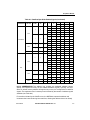
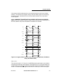
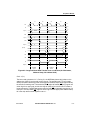
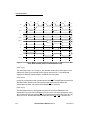
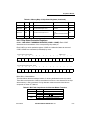
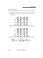
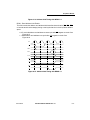
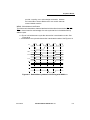
Chip-Select Module
.
C1
C2
C3
C4
C5
CLK
TS
A[27:0]
$ADDR
$ADDR + 2
R/W
SIZ[1:0]
$0
D[31:16]
TA
TEA
ATA
CS
WE[3:0]
Figure 8-10. Alternate Master Longword Read Transfer from a 16-Bit Port (No Wait
State, With Address Setup Or Read Address Hold)
Clock 1 (C1)
The read cycle starts in C1. During C1, the alternate master places valid values on the
address bus (A[27:0]) and transfer control signals. At the end of C1, the MCF5206
registers the alternate master address, read/write and size signals.
Clock 2 (C2)
During C2, the alternate master negates transfer start (TS). The MCF5206 compares the
alternate master address to the internal chip-select addresses and enables the
appropriate chip-select and transfer acknowledge (TA) for assertion.
Clock 3 (C3)
The MCF5206 asserts the appropriate chip-select and since the EMAA bit in the
appropriate Chip-select Control Register (CSCR) is set to one and wait states are set to
zero, asserts transfer acknowledge (TA). The selected device drives data onto D[31:16].
At the end of C3, the alternate master samples the level of TA. If TA is asserted, the
8-26
MCF5206 USERÕS MANUAL Rev 1.0
MOTOROLA