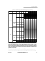
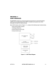
1
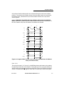
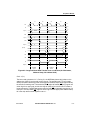
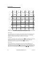
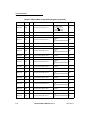
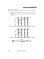
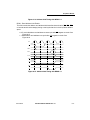
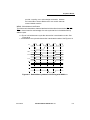
Chip-Select Module
Chip-Select Mask Register(CSMR2 - CSMR7)
31
30
29
28
27
26
25
24
23
22
21
20
19
18
17
16
BAM31 BAM30 BAM29 BAM28 BAM27 BAM26 BAM25 BAM24 BAM23 BAM22 BAM21 BAM20 BAM19 BAM18 BAM17 BAM16
RESET:
-
-
-
-
-
-
-
-
-
-
-
-
-
-
-
-
15
14
13
12
11
10
9
8
7
6
5
4
3
2
1
0
-
-
-
-
-
-
-
-
-
-
-
SC
SD
UC
UD
-
0
0
0
0
0
0
0
0
0
0
-
-
-
-
0
RESET:
0
BAM31-BAM16 - Base Address Mask
This field defines the chip-select block size through the use of address mask bits. Any bit
set to 1 masks the corresponding base address register (CSAR) bit (the base address bit
becomes a ÔÔdonÕt careÕÕ in the decode).
0 = Corresponding address bit is used in chip-select address decode.
1 = Corresponding address bit is not used in chip-select address decode.
C/I, SC, SD, UC, UD - CPU Space, Supervisor Code, Supervisor Data, User Code, User
Data Transfer Mask
These fields allows specific types of transfers to be inhibited from accessing a chip-select.
If a transfer mask bit is cleared, a transfer of that type can access the corresponding chipselect. If a transfer mask bit is set to 1, an transfer of that type can not access the
corresponding chip-select. The transfer mask bits are:
C/I = CPU space and Interrupt Acknowledge Cycle mask (CS[1] only)
SC = Supervisor Code mask
SD = Supervisor Data mask
UC = User Code mask
UD = User Data mask
For each transfer mask bit:
0 = Do not mask this type of transfer for the chip-select. A transfer of this type can
occur for this chip-select.
1 = Mask this type of transfer from the chip-select. If this type of transfer is generated,
this chip-select activation will not be activated.
NOTE
The C/I, SC, SD, UC, and UD bits are ignored during alternate
master transfers. Therefore, an alternate master transfer can
activate a chip-select regardless of the transfer masks.
MOTOROLA
MCF5206 USERÕS MANUAL Rev 1.0
8-31