1
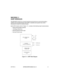
1
2
SECTION 12
M-BUS MODULE
4
12.1 OVERVIEW
Motorola bus (M-Bus) is a two-wire, bidirectional serial bus that provides a simple, efficient
method of data exchange between devices. It is compatible with the widely used I2C bus
standard1. This two-wire bus minimizes the interconnection between devices.
5
This bus is suitable for applications requiring occasional communications over a short
distance between many devices. The flexible M-Bus allows additional devices to be
connected to the bus for expansion and system development.
6
The interface operates up to 100 kbps with maximum bus loading and timing.
7
The M-Bus system is a true multimaster bus including collision detection and arbitration that
prevents data corruption if two or more masters attempt to control the bus simultaneously.
This feature allows for complex applications with multiprocessor control. It can also be used
for rapid testing and alignment of end products via external connections to an assembly line
computer.
8
9
12.2 INTERFACE FEATURES
The M-Bus module has the following key features:
2C
¥ Compatibility with I
10
Bus standard
¥ Multimaster operation
11
¥ Software-programmable for one of 64 different serial clock frequencies
¥ Software-selectable acknowledge bit
12
¥ Interrupt-driven byte-by-byte data transfer
¥ Arbitration-lost interrupt with automatic mode switching from master to slave
13
¥ Calling address identification interrupt
¥ Start and stop signal generation/detection
¥ Repeated START signal generation
14
¥ Acknowledge bit generation/detection
¥ Bus-busy detection
1. 2
I C-Bus is a proprietary Philips interface bus.
MOTOROLA
MCF5206 USERÕS MANUAL Rev 1.0
16
12-1
M-Bus Module
1
A block diagram of the complete M-Bus Module is shown in Figure 12-1.
2
ADDR
IRQ
DATA
REGISTERS AND COLDFIRE INTERFACE
ADDR_DECODE
DATA_MUX
4
5
CTRL_REG
FREQ_REG
ADDR_REG
DATA_REG
STATUS_REG
6
7
INPUT
SYNC
IN/OUT
DATA SHIFT
REGISTER
START, STOP, AND
ARBITRATION
CONTROL
8
9
CLOCK
CONTROL
ADDRESS
COMPARE
10
11
SCL
12
13
14
15
SDA
Figure 12-1. M-Bus Module Block Diagram
12.3 M-BUS SYSTEM CONFIGURATION
The M-Bus system uses a serial data line (SDA) and a serial clock line (SCL) for data
transfer. All devices connected to these two signals must have open drain or open collector
outputs. The logic AND function is exercised on both lines with pullup resistors.
The default state of the M-Bus is as a slave reciever out of reset. Thus, when not
programmed to be a master or responding to a slave transmit address, the M-Bus should
always return to the default state of slave receiver.
16
12-2
MCF5206 USERÕS MANUAL Rev 1.0
MOTOROLA
M-Bus Module
1
NOTE
For further information on M-Bus system configuration, protocol,
and restrictions please refer to the PhilipÕs I2C standard
2
12.4 M-BUS PROTOCOL
Normally, a standard communication is composed of four parts: (1) START signal, (2) slave
address transmission, (3) data transfer, and (4) STOP signal. They are described briefly in
the following sections and illustrated in Figure 12-2.
MSB
SCL
SDA
1
LSB
2
3
4
5
6
7
CALLING ADDRESS
1
XXX
2
3
4
5
CALLING ADDRESS
3
4
5
6
7
8
D7
D6
D5
D4
D3
D2
D1
D0
6
7
8
9
READ/ ACK
WRITE BIT
1
XX
AD7
REPEATED
START
SIGNAL
9
6
NO STOP
ACK SIGNAL
BIT
LSB
MSB
AD7 AD6 AD5 AD4 AD3 AD2 AD1 R/W
START
SIGNAL
2
DATA BYTE
LSB
4
LSB
1
READ/ ACK
WRITE BIT
MSB
SDA
MSB
9
AD7 AD6 AD5 AD4 AD3 AD2 AD1 R/W
START
SIGNAL
SCL
8
3
2
3
4
5
6
7
8
7
8
9
9
AD6 AD5 AD4 AD3 AD2 AD1 R/W
NEW CALLING ADDRESS READ/WRITE NO STOP
ACK SIGNAL
BIT
10
11
Figure 12-2. M-Bus Standard Communication Protocol
12.4.1 START Signal
12
When the bus is free, i.e., no master device is engaging the bus (both SCL and SDA lines
are at logic high), a master can initiate communication by sending a START signal. As
shown in Figure 12-2, a START signal is defined as a high-to-low transition of SDA while
SCL is high. This signal denotes the beginning of a new data transfer (each data transfer
can contain several bytes of data) and awakens all slaves.
13
12.4.2 Slave Address Transmission
14
The first byte of data transfered by the master immediately after the START signal is the
slave address. This is a seven-bit calling address followed by a R/W bit. The R/W bit tells
the slave data transfer direction. No two slaves in the system can have the same address.
16
MOTOROLA
MCF5206 USERÕS MANUAL Rev 1.0
12-3
M-Bus Module
1
2
In addition, if the M-Bus is master, it must not transmit an address that is equal to its slave
address. The M-Bus cannot be master and slave at the same time.
Only the slave with a calling address that matches the one transmitted by the master will
respond by returning an acknowledge bit by pulling the SDA low at the 9th clock (see Figure
12-2).
12.4.3 Data Transfer
4
Once successful slave addressing is achieved, the data transfer can proceed on a byte-bybyte basis in the direction specified by the R/W bit sent by the calling master.
6
Each data byte is 8 bits long. Data can be changed only while SCL is low and must be held
stable while SCL is high, as shown in Figure 12-2. There is one clock pulse on SCL for each
data bit with the MSB being transferred first. Each byte data must be followed by an
acknowledge bit, which is signalled from the receiving device by pulling the SDA low at the
ninth clock. One complete data byte transfer needs nine clock pulses.
7
If the slave receiver does not acknowledge the master, the SDA line must be left high by the
slave. The master can then generate a stop signal to abort the data transfer or a start signal
(repeated start) to commence a new calling.
8
If the master receiver does not acknowledge the slave transmitter after a byte transmission,
it means 'Ôend of data'Õ to the slave. The slave releases the SDA line for the master to
generate STOP or START signal.
9
12.4.4 Repeated START Signal
5
10
As shown in Figure 12-2, a repeated START signal is a START signal generated without
first generating a STOP signal to terminate the communication. The master uses this
method to communicate with another slave or with the same slave in different mode
(transmit/receive mode) without releasing the bus.
11
12.4.5 STOP Signal
12
13
The master can terminate the communication by generating a STOP signal to free the bus.
However, the master can generate a START signal followed by a calling command without
generating a STOP signal first. This is called repeated START. A STOP signal is defined as
a low-to-high transition of SDA while SCL at logical Ò1Ó (see Figure 12-2). Note that a master
can generate a STOP even if the slave has done an acknowledgement at which point the
slave must release the bus.
12.4.6 Arbitration Procedure
14
15
M-Bus is a true multimaster bus that allows more than one master to be connected on it. If
two or more masters try to simultaneously control the bus, a clock synchronization
procedure determines the bus clock, for which the low period is equal to the longest clock
low period and the high is equal to the shortest one among the masters. A data arbitration
procedure determines the relative priority of the contending masters. A bus master loses
arbitration if it transmits logic Ò1Ó while another master transmits logic Ò0.Ó The losing masters
16
12-4
MCF5206 USERÕS MANUAL Rev 1.0
MOTOROLA
M-Bus Module
immediately switch over to slave-receive mode and stop driving SDA output. In this case,
the transition from master to slave mode does not generate a STOP condition. Meanwhile,
hardware sets a status bit to indicate loss of arbitration.
1
2
12.4.7 Clock Synchronization
Because wire-AND logic is performed on SCL line, a high-to-low transition on SCL line
affects all the devices connected on the bus. The devices start counting their low period
when the master drives the SCL line low. Once a device clock has gone low, it holds the
SCL line low until the clock high state is reached. However, the change of low to high in this
device clock may not change the state of the SCL line if another device clock is still within
its low period. Therefore, synchronized clock SCL is held low by the device with the longest
low period. Devices with shorter low periods enter a high wait state during this time (see
Figure 12-3). When all devices concerned have counted off their low period, the
synchronized clock SCL line is released and pulled high. There is then no difference
between the device clocks and the state of the SCL line and all the devices start counting
their high periods. The first device to complete its high period pulls the SCL line low again.
WAIT
3
4
6
7
START COUNTING HIGH PERIOD
SCL1
8
SCL2
9
SCL
10
11
INTERNAL COUNTER RESET
12
Figure 12-3. Synchronized Clock SCL
12.4.8 Handshaking
The clock synchronization mechanism can be used as a handshake in data transfer. Slave
devices can hold the SCL low after completion of one byte transfer (9 bits). In such cases,
it halts the bus clock and forces the master clock into wait states until the slave releases the
SCL line.
13
14
12.4.9 Clock Stretching
Slaves can use the clock synchronization mechanism to slow down the transfer bit rate.
After the master has driven SCL low the slave can drive SCL low for the required period and
16
MOTOROLA
MCF5206 USERÕS MANUAL Rev 1.0
12-5
M-Bus Module
1
2
then release it. If the slave SCL low period is greater than the master SCL low period,the
resulting SCL bus signal low period is stretched.
12.5 PROGRAMMING MODEL
Five registers are used in the M-Bus interface and the internal configuration of these
registers is discussed in the following paragraphs.The programmerÕs model of the M-Bus
interface is shown below in Table 12-1.
Table 12-1. M-Bus Interface ProgrammerÕs Model
4
5
6
ADDRESS
M-BUS MODULE REGISTERS
MBAR+$1E0
M-Bus Address register (MADR)
MBAR+$1E4
M-Bus Frequency Divider Register (MFDR)
MBAR+$1E8
M-Bus Control Register (MBCR)
MBAR+$1EC
M-Bus Status Register (MBSR)
MBAR+$1F0
M-Bus Data I/O Register (MBDR)
A block diagram of the M-Bus system is shown in Figure 12-1.
7
8
12.5.1 M-Bus Address Register (MADR)
This register contains the address the M-Bus will respond to when addressed as a slave;
note that it is not the address sent on the bus during the address transfer.
M-Bus Address Register (MADR)
9
RESET
10
11
Address MBAR+$1E0
7
6
5
4
3
2
1
ADR7
ADR6
ADR5
ADR4
ADR3
ADR2
ADR1
-
0
0
0
0
0
0
0
0
Read/Write
0
Supervisor or User Mode
ADR7ÐADR1 Ñ Slave Address
Bits1 to 7 contain the specific slave address to be used by the M-Bus module.
NOTE
The default mode of M-Bus is slave mode for an address match
on the bus.
12
12.5.2 M-Bus Frequency Divider Register (MFDR)
13
M-Bus Frequency Divider Register
(MFDR)
14
RESET
7
6
5
4
3
2
1
0
-
-
MBC5
MBC4
MBC3
MBC2
MBC1
MBC0
0
0
0
0
0
0
0
0
Read/Write
15
16
Address MBAR+$1E4
Supervisor or User Mode
MBC5ÐMBC0 Ñ M-Bus Clock Rate 5Ð0
This field is used to prescale the clock for bit rate selection. Due to the potential slow rise
and fall times of the SCL and SDA signals, the bus signals are sampled at the prescaler
12-6
MCF5206 USERÕS MANUAL Rev 1.0
MOTOROLA
M-Bus Module
frequency. The serial bit clock frequency is equal to the CPU clock divided by the divider
shown in Table 12-2, which also shows the serial bit clock frequency for a 33MHz internal
operating frequency2. Note that the MFDR frequency value can be changed at any point
in a program.
DIVIDER
(DEC)
MBC5-0
(HEX)
DIVIDER
(DEC)
00
01
02
03
04
05
06
07
08
09
0A
0B
0C
0D
0E
0F
10
11
12
13
14
15
16
17
18
19
1A
1B
1C
1D
1E
1F
28
30
34
40
44
48
56
68
80
88
104
128
144
160
192
240
288
320
384
480
576
640
768
960
1152
1280
1536
1920
2304
2560
3072
3840
20
21
22
23
24
25
26
27
28
29
2A
2B
2C
2D
2E
2F
30
31
32
33
34
35
36
37
38
39
3A
3B
3C
3D
3E
3F
20
22
24
26
28
32
36
40
48
56
64
72
80
96
112
128
160
192
224
256
320
384
448
512
640
768
896
1024
1280
1536
1792
2048
2
3
Table 12-2. MBUS Prescalar Values
MBC5-0
(HEX)
1
4
6
7
8
9
10
11
12
13
14
2.
In previous implementations of the M-Bus (e.g., MC68307), the MBC[5] bit was not implemented. Clearing
this bit in software maintains complete compatibility with such products.
MOTOROLA
MCF5206 USERÕS MANUAL Rev 1.0
12-7
16
M-Bus Module
1
12.5.3 M-Bus Control Register (MBCR)
M-Bus Control Register (MBCR)
2
RESET
6
5
4
3
2
1
MEN
MIEN
MSTA
MTX
TXAK
RSTA
-
0
0
0
0
0
0
0
Read/Write
4
7
8
9
10
11
12
13
14
0
0
Supervisor or User Mode
MEN Ñ M-Bus Enable
This bit controls the software reset of the entire M-Bus module.
1 = The M-Bus module is enabled. This bit must be set before any other MBCR bits
have any effect.
0 = The module is reset and disabled. This is the power-on reset situation. When low,
the interface is held in reset but registers can still be accessed.
5
6
Address MBAR+$1E8
7
If the M-Bus module is enabled in the middle of a byte transfer, the interface behaves as
follows: the slave mode ignores the current transfer on the bus and starts operating
whenever a subsequent start condition is detected. Master mode will not be aware that the
bus is busy; therefore, if a start cycle is initiated, the current bus cycle can become corrupt.
This would ultimately result in either the current bus master or the M-Bus module losing
arbitration, after which bus operation would return to normal.
MIEN Ñ M-Bus Interrupt Enable
1 = Interrupts from the M-Bus module are enabled. An M-Bus interrupt occurs provided
the MIF bit in the status register is also set.
0 = Interrupts from the M-Bus module are disabled. This does not clear any currently
pending interrupt condition.
MSTA Ñ Master/Slave Mode Select Bit
At reset, this bit is cleared. When this bit is changed from 0 to 1, a START signal is generated
on the bus, and the master mode is selected. When this bit is changed from 1 to 0, a STOP
signal is generated and the operation mode changes from master to slave.
MSTA is cleared without generating a STOP signal when the master loses arbitration.
1 = Master Mode
0 = Slave Mode
MTX Ñ Transmit/Receive mode select bit
This bit selects the direction of master and slave transfers. When addressed as a slave this
bit should be set by software according to the SRW bit in the status register. In master mode,
this bit should be set according to the type of transfer required. Therefore, for address
cycles, this bit will always be high.
1 = Transmit
0 = Receive
15
16
12-8
MCF5206 USERÕS MANUAL Rev 1.0
MOTOROLA
M-Bus Module
TXAK Ñ Transmit Acknowledge Enable
This bit specifies the value driven onto SDA during acknowledge cycles for both master and
slave receivers. Note that writing this bit only applies when the M-Bus is a receiver, not a
transmitter.
1
2
1 = No acknowledge signal response is sent (i.e., acknowledge bit = 1)
0 = An acknowledge signal will be sent out to the bus at the 9th clock bit after receiving
one byte data
3
RSTA Ñ Repeat Start
Writing a 1 to this bit will generate a repeated START condition on the bus, provided it is the
current bus master. This bit will always be read as a low. Attempting a repeated start at the
wrong time, if the bus is owned by another master, will result in loss of arbitration. Note that
this bit is not readable.
4
6
1 = Generate repeat start cycle
12.5.4 M-Bus Status Register (MBSR)
This status register is read-only with the exception of bit 1 (MIF) and bit 4 (MAL), which can
be cleared by software. All bits are cleared on reset except bit 7 (MCF) and bit 0 (RXAK),
which are set (=1) at reset.
M-Bus Status Register (MBSR)
RESET
7
6
5
4
3
2
1
0
MAAS
MBB
MAL
-
SRW
MIF
RXAK
1
0
0
0
0
0
0
1
Read/Write
8
Address MBAR+$1EC
MCF
7
9
Supervisor or User Mode
MCF Ñ Data Transferring Bit
While one byte of data is being transferred, this bit is cleared. It is set by the falling edge of
the 9th clock of a byte transfer.
1 = Transfer complete
0 = Transfer in progress
10
11
12
MAAS Ñ Addressed as a Slave Bit
When its own specific address (M-Bus Address Register) is matched with the calling
address, this bit is set. The CPU is interrupted provided the MIEN is set. Next, the CPU must
check the SRW bit and set its TX/RX mode accordingly.
Writing to the M-Bus Control Register clears this bit.
1 = Addressed as a slave
0 = Not addressed
13
14
16
MOTOROLA
MCF5206 USERÕS MANUAL Rev 1.0
12-9
M-Bus Module
1
2
MBB Ñ Bus Busy Bit
This bit indicates the status of the bus. When a START signal is detected, the MBB is set. If
a STOP signal is detected, it is cleared.
1 = Bus is busy
0 = Bus is idle
4
MAL Ñ Arbitration Lost
Hardware sets the arbitration lost bit (MAL) when the arbitration procedure is lost. Arbitration
is lost in the following circumstances:
5
1. SDA sampled as low when the master drives a high during an address or data-transmit
cycle.
6
2. SDA sampled as a low when the master drives a high during the acknowledge bit of a
data-receive cycle.
3. A start cycle is attempted when the bus is busy.
4. A repeated start cycle is requested in slave mode.
7
5. A stop condition is detected when the master did not request it.
This bit must be cleared by software by writing a low to it.
8
9
10
SRW Ñ Slave Read/Write
When MAAS is set, this bit indicates the value of the R/W command bit of the calling address
sent from the master. This bit is valid only when 1) a complete transfer has occurred and no
other transfers have been initiated and 2) M-Bus is a slave and has an address match.
Checking this bit, the CPU can select slave transmit/receive mode according to the
command of the master.
1 = Slave transmit, master reading from slave
0 = Slave receive, master writing to slave
11
12
MIF Ñ M-Bus Interrupt
The MIF bit is set when an interrupt is pending, which will cause a processor interrupt
request (provided MIEN is set). MIF is set when one of the following events occurs:
1. Complete one byte transfer (set at the falling edge of the 9th clock)
13
2. Receive a calling address that matches its own specific address in slave-receive mode
3. Arbitration lost
14
This bit must be cleared by software by writing a low to it in the interrupt routine.
15
RXAK Ñ Received Acknowledge
The value of SDA during the acknowledge bit of a bus cycle. If the received acknowledge
bit (RXAK) is low, it indicates an acknowledge signal has been received after the completion
16
12-10
MCF5206 USERÕS MANUAL Rev 1.0
MOTOROLA
M-Bus Module
of 8 bits data transmission on the bus. If RXAK is high, it means no acknowledge signal has
been detected at the 9th clock.
2
1 = No acknowledge received
0 = Acknowledge received
3
12.5.5 M-Bus Data I/O Register (MBDR)
M-Bus Data I/O Register (MBDR)
RESET
Address MBAR+$1F0
7
6
5
4
3
2
1
0
D7
D6
D5
D4
D3
D2
D1
D0
0
0
0
0
0
0
0
0
Read/Write
1
4
Supervisor or User Mode
When an address and R/W bit is written to the MBDR and the M-Bus is the master, a
transmission will start. When data is written to the MBDR, a data transfer is initiated. The
most significant bit is sent first in both cases. In the master receive mode, reading the MBDR
register allows the read to occur but also initiates next byte data receiving. In slave mode,
the same function is available after it is addressed.
6
7
12.6 M-BUS PROGRAMMING EXAMPLES
12.6.1 Initialization Sequence
Reset will put the M-bus Control Register to its default status. Before the interface can
transfer serial data, you must perform an initialization procedure as follows:
1. Update the Frequency Divider Register (MFDR) and select the required division ratio
to obtain SCL frequency from system clock.
2. Update the M-Bus Address Register (MADR) to define its slave address.
8
9
10
3. Set the MEN bit of the M-Bus Control Register (MBCR) to enable the M-Bus interface
system.
4. Modify the bits of the M-Bus Control Register (MBCR) to select master/slave mode,
transmit/receive mode, and interrupt-enable or not.
11
12.6.2 Generation of START
12
After completion of the initialization procedure, you can transmit serial data by selecting the
'Ômaster transmitter'Õ mode. If the device is connected to a multi-master bus system, you
must test the state of the M-Bus Busy Bit (MBB) to check whether the serial bus is free.
13
If the bus is free (MBB=0), the start condition and the first byte (the slave address) can be
sent. The data written to the data register comprises the slave-calling address and the LSB
set to indicate the direction of transfer required from the slave.
14
The bus free time (i.e., the time between a STOP condition and the following START
condition) is built into the hardware that generates the START cycle. Depending on the
relative frequencies of the system clock and the SCL period, you may have to wait until the
16
MOTOROLA
MCF5206 USERÕS MANUAL Rev 1.0
12-11
M-Bus Module
1
2
4
5
6
7
M-Bus is busy after writing the calling address to the MBDR before proceeding with the
following instructions.
An example of a program that generates the START signal and transmits the first byte of
data (slave address) is shown below:
CHFLAGMOVE.BMBSR,-(A7);
BTST.B#5, (A7)+
BNE.SCHFLAG;
CHECK THE MBB BIT OF THE STATUS REGISTER. IF IT IS
SET, WAIT UNTIL IT IS CLEAR
TXSTARTMOVE.BMBCR,-(A7);
BSET.B#4,(A7)
SET TRANSMIT MODE
MOVE.B(A7)+, MBCR
MOVE.BMBCR, -(A7);
BSET.B#5, (A7);
MOVE.B(A7)+, MBCR;
MOVE.BCALLING,-(A7);
MOVE.B(A7)+, MBDR;
MBFREEMOVE.BMBSR,-(A7);
BTST.B#5, (A7)+;
BEQ.SMBFREE;
SET MASTER MODE
i.e. GENERATE START CONDITION
TRANSMIT THE CALLING ADDRESS, D0=R/W
CHECK THE MBB BIT OF THE STATUS REGISTER. IF IT IS
CLEAR, WAIT UNTIL IT IS SET
8
12.6.3 Post-Transfer Software Response
9
Transmission or reception of a byte will set the data transferring bit (MCF) to 1, which
indicates one byte communication is finished. The M-Bus interrupt bit (MIF) is also set ; an
interrupt will be generated if the interrupt function is enabled during initialization by setting
the MIEN bit. Software must clear the MIF bit in the interrupt routine first. The MCF bit will
be cleared by reading from the M-Bus Data I/O Register (MDR) in receive mode or writing
to MDR in transmit mode.
10
11
12
13
14
15
Software can service the M-bus I/O in the main program by monitoring the MIF bit if the
interrupt function is disabled. Polling should monitor the MIF bit rather than the MCF bit
because that operation is different when arbitration is lost.
When an interrupt occurs at the end of the address cycle, the master will always be in
transmit mode, i.e. the address is transmitted. If master receive mode is required, indicated
by R/W bit in MBDR, then the MTX bit should be toggled at this stage.
During slave-mode address cycles (MAAS=1), the SRW bit in the status register is read to
determine the direction of the subsequent transfer and the MTX bit is programmed
accordingly. For slave-mode data cycles (MAAS=0), the SRW bit is not valid. The MTX bit
in the control register should be read to determine the direction of the current transfer.
The following is an example of a software response by a 'Ômaster transmitterÕ' in the interrupt
routine (see Figure 12-4).
16
12-12
MCF5206 USERÕS MANUAL Rev 1.0
MOTOROLA
M-Bus Module
1
ISRLEA.LMBSR,-(A7);
BCLR.B#1,(A7)+;
MOVE.BMBCR,-(A7);
BTST.B#5,(A7)+;
BEQ.SSLAVE;
MOVE.BMBCR,-(A7);
BTST.B#4,(A7)+;
BEQ.SRECEIVE;
MOVE.BMBSR,-(A7);
BTST.B#0,(A7)+;
BNE.B END;
TRANSMITMOVE.BDATABUF,-(A7);
MOVE.B(A7)+, MBDR;
LOAD EFFECTIVE ADDRESS
CLEAR THE MIF FLAG
PUSH ADDRESS ON STACK,
CHECK THE MSTA FLAG
BRANCH IF SLAVE MODE
PUSH ADDRESS ON STACK
CHECK THE MODE FLAG
BRANCH IF IN RECEIVE MODE
PUSH ADDRESS ON STACK,
CHECK ACK FROM RECEIVER
IF NO ACK, END OF TRANSMISSION
STACK DATA BYTE
TRANSMIT NEXT BYTE OF DATA
2
3
4
12.6.4 Generation of STOP
A data transfer ends with a STOP signal generated by the 'ÔmasterÕ' device. A master
transmitter can generate a STOP signal after all the data has been transmitted. The
following is an example showing how a master transmitter generates a stop condition.
MASTXMOVE.BMBSR, -(A7);
BTST.B#0,(A7)+
BNE.B END
MOVE.BTXCNT,D0;
BEQ.SEND;
MOVE.BDATABUF,-(A7);
MOVE.B(A7)+,MBDR
MOVE.BTXCNT,D0;
SUBQ.L#1,D0
MOVE.BD0,TXCNT
BRA.SEMASTX;
ENDLEA.LMBCR,-(A7);
BCLR.B#5,(A7)+
EMASTXRTE;
6
IF NO ACK, BRANCH TO END
7
GET VALUE FROM THE TRANSMITTING COUNTER
IF NO MORE DATA, BRANCH TO END
TRANSMIT NEXT BYTE OF DATA
8
DECREASE THE TXCNT
9
EXIT
GENERATE A STOP CONDITION
10
RETURN FROM INTERRUPT
If a master receiver wants to terminate a data transfer, it must inform the slave transmitter
by not acknowledging the last byte of data, which can be done by setting the transmit
acknowledge bit (TXAK) before reading the 2nd last byte of data. Before reading the last
byte of data, a STOP signal must be generated first. The following is an example showing
how a master receiver generates a STOP signal.
MASRMOVE.BRXCNT,D0;
SUBQ.L#1,D0
MOVE.BD0,RXCNT
BEQ.SENMASR;
MOVE.BRXCNT,D1;
EXTB>LD1
SUBI.L#1,D1;
BNE.SNXMAR
LAMARBSET.B#3,MBCR;
BRANXMAR
MOTOROLA
11
12
13
DECREASE RXCNT
LAST BYTE TO BE READ
CHECK SECOND LAST BYTE TO BE READ (NOT LAST ONE OR SECOND
LAST
14
SECOND LAST, DISABLE ACK TRANSMITTING
16
MCF5206 USERÕS MANUAL Rev 1.0
12-13
M-Bus Module
1
ENMASRBCLR.B#5,MBCR;
LAST ONE, GENERATE 'STOPÕ SIGNAL
NXMARMOVE.BMBDR,RXBUF; READ DATA AND STORE RTE
2
12.6.5 Generation of Repeated START
At the end of data transfer, if the master still wants to communicate on the bus, it can
generate another START signal followed by another slave address without first generating
a STOP signal. A program example is as shown.
4
5
6
7
8
9
10
11
RESTARTMOVE.BMBCR,-(A7); ANOTHER START (RESTART)
BSET.B#2, (A7)
MOVE.B(A7)+, MBCR
MOVE.BCALLING,-(A7);
TRANSMIT THE CALLING ADDRESS, D0=R/WMOVE.BCALLING,-(A7);
MOVE.B(A7)+, MBDR
12.6.6 Slave Mode
In the slave interrupt service routine, the module addressed as slave bit (MAAS) should be
tested to check if a calling of its own address has just been received. If MAAS is set, software
should set the transmit/receive mode select bit (MTX bit of MBCR) according to the R/W
command bit (SRW). Writing to the MBCR clears the MAAS automatically. The only time
MAAS is read as set is from the interrupt at the end of the address cycle where an address
match occurred; interrupts resulting from subsequent data transfers will have MAAS
cleared. A data transfer can now be initiated by writing information to MBDR, for slave
transmits, or dummy reading from MBDR, in slave-receive mode. The slave will drive SCL
low in between byte transfers. SCL is released when the MBDR is accessed in the required
mode.
In slave transmitter routine, the received acknowledge bit (RXAK) must be tested before
transmitting the next byte of data. Setting RXAK means an 'Ôend-of-dataÕ' signal from the
master receiver, after which it must be switched from transmitter mode to receiver mode by
software. A dummy read then releases the SCL line so that the master can generate a STOP
signal.
12
12.6.7 Arbitration Lost
13
14
15
16
If several masters try to simultaneously engage the bus, only one master wins and the
others lose arbitration. The devices that lost arbitration are immediately switched to slave
receive mode by the hardware. Their data output to the SDA line is stopped, but SCL is still
generated until the end of the byte during which arbitration was lost. An interrupt occurs at
the falling edge of the ninth clock of this transfer with MAL=1 and MSTA=0. If one master
tries to transmit or do a START while the bus is being engaged by another master, the
hardware will: (1) inhibit the transmission, (2) switch the MSTA bit from 1 to 0 without
generating STOP condition, (3) generate an interrupt to CPU and, (4) set the MAL to indicate
the failed attempt to engage the bus. When considering these cases, the slave service
routine should test the MAL first and the software should clear the MAL bit if it is set.
12-14
MCF5206 USERÕS MANUAL Rev 1.0
MOTOROLA
M-Bus Module
1
2
CLEAR
MIF
Y
TX
LASTBYTE
TRANSMITTED
?
MASTER
MODE
?
3
N
Y
RX
TX/RX
?
4
ARBITRATION
LOST
?
N
CLEARMAL
Y
N
RXAK=0
?
LAST
BYTETOBEREAD
?
N
Y
N
Y
Y
6
N
ENDOF
ADDRCYCLE
(MASTERRX)
?
N
WRITENEXT
BYTETOMBDR
Y
Y
(READ)
N
SRW=1
?
GENERATE
STOPSIGNAL
SWITCHTO
RXMODE
GENERATE
STOPSIGNAL
READDATA
FROMMBDR
ANDSTORE
RX
8
TX
Y
SETTX
MODE
7
DATA
CYCLE
TX/RX
?
N (WRITE)
N
ACKFROM
RECEIVER
?
N
9
READDATA
FROMMBDR
ANDSTORE
TXNEXT
BYTE
WRITEDATA
TOMBDR
DUMMYREAD
FROMMBDR
MAAS=1
?
ADDRESSY
CYCLE
2NDLAST
BYTETOBEREAD
?
SETTXAK=1
Y
MAAS=1
?
SETRX
MODE
SWITCHTO
RXMODE
DUMMYREAD
FROMMBDR
DUMMYREAD
FROMMBDR
10
11
12
13
RTE
14
Figure 12-4. Flow-Chart of Typical M-Bus Interrupt Routine
16
MOTOROLA
MCF5206 USERÕS MANUAL Rev 1.0
12-15