1
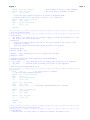
EE/CS 52 Digital Oscilloscope Documentation
Julian Panetta
TA: Gabe Cohn
Table of Contents
•
•
•
•
•
•
•
•
•
•
•
User’s manual
Functional Specification
Block Diagram
Protoboard Schematic
Board Layout
Timing Diagrams
o VRAM
Timing Specifications
Read, Write, Refresh, Data Transfer
o LCD
Timing Specifications
LCD Signals
o SRAM
Read, Write
o Rom
Read
Memory Map
Pin Assignment
Quartus Design
o Top Level Design
o Analog Control Block
o LCD/VRAM Control Block
o LCD Signal Generator
o Keypad Debouncer
o Clock Divider
VHDL
o VRAM Controller State Machine
State machine diagram
vram_controller_lut.vhd
o split.vhd, combine.vhd, combine_16_16.vhd
Software
o Drivers/Initialization
start.s
keypad.s, display.s, interrupts.s
constants.s
o OS
stubfuncs.c
interfac.h
Julian
Panetta
TA:
Gabe
Cohn
EE/CS
52
Digital Oscilloscope
User’s Manual
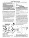
Introduction
This digital oscilloscope is an easy-to-use instrument for visualizing analog input
signals. In fact, such great care has been taken to ensure ease of use that the user’s task of
finding and attaching an analog voltage signal source has been removed entirely. Simply
attach the oscilloscope to a computer, open up your $2500+ copy of Quartus, program the
FPGA design into it, and you’re ready to view the beautiful, noise-free built-in simulated
signal. Even better, there is no need to try to figure out how switch to another input signal
because this oscilloscope has been specialized to display only this signal!
Hardware
The hardware devices you use to interact with and monitor the oscilloscope are
described on the next page.
Page
1
Julian
Panetta
TA:
Gabe
Cohn
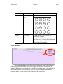
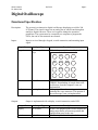
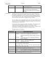
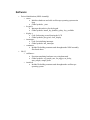
Device Name
Keypad
EE/CS
52
Page
2
Device Type
4*4 Array of 16
keys
Description
Of the 16 keys, only 5 are used:
Up
Left
Menu
Right
Down
Display
LCD Panel
Status LED
LED
A “high” quality LCD to display the
oscilloscope’s output.
A shiny red LED that lights when system
has booted to let you know that initialization
has completed successfully and the scope
interface should be running.
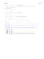
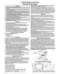
User Interface
Menu
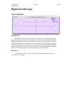
Once programmed, the system boots into Normal mode with a 100ns sampling
rate and a positive slope mid-level (2.480V) trigger with no delay. x- and y-axes are
displayed behind the trace, and a menu in the upper right-hand corner—demonstrated in
the screenshot above—lets you change all of the scope’s settings and enter different
sampling modes. To hide and show the menu, press the <Menu> key.
Julian
Panetta
TA:
Gabe
Cohn
EE/CS
52
You can change from one highlighted menu item to the next using the <Up> and
<Down> keys. To alter the highlighted configuration setting, the user presses the <Left>
and <Right> keys to select a value.
The configurable settings and their values are as follows:
Menu Title
Mode
Scale
Sweep
Level
Slope
Delay
Options and Description
Normal
Scope waits for a trigger after completing each
retrace.
Automatic Scope waits for a trigger after each retrace, but
retriggers automatically without a trigger event
after a delay.
One-Shot
Scope triggers only once, continuing to display
the last trace captured.
Scale Axes Display x and y axes along with trace.
Scale Grid Display x-y grid along with the trace.
Scale Off
Display the trace only.
Items are time quantities that specify the sweep rate, or the
time between successive samples options:
100ns, 200ns, 500ns, 1us, 2us, 5us, 10us, 20us, 50us, 100us,
200us, 500us, 1ms, 2ms, 5ms, 10ms, 20ms
128 voltage quantities are given as choices for the trigger
voltage level. The levels are equally spaced from 0V to 5V.
Slope +
Scope is triggered on a positive slope (rising
edge)
Slope Scope is triggered on a negative slope (falling
edge)
Time quantities ranging between 0ms and 1ms specify the
time between the trigger and the start of the trace.
Limitations
If for some reason you have decided to go through the effort of finding a voltage
source you want to measure, you will find that the oscilloscope has no connector to which
you can attach the signal. The oscilloscope is compatible only with the built-in
demonstration trace.
Page
3
Julian
Panetta
TA:
Gabe
Cohn
EE/CS
52
Page
1
Digital Oscilloscope
Functional Specification
Description:
The system is an interactive digital oscilloscope displaying on a 640 x 200
LCD panel. The signal is input via an analog line in, which runs through an
analog to digital converter. There is a keypad to change the operation
parameters. The system must be connected to a computer to program the
FPGA, but can be disconnected once booted.
Inputs:
Input is received through a keypad, a serial connection, and an analog input
signal.
Input Name
Keypad
Input Type
4*4 Array of 16
keys
Description
Of the 16 keys, only 5 are used by the OS:
Up
Left
Menu
Right
Down
Serial
RS-232 Port
Analog
Analog Line In
Outputs:
Allows communication with the NIOS using
GERMS. Downloading of sample data to the
oscilloscope from the computer is not yet
implemented.
Analog signal line whose voltage variation
with time the scope measures. This portion of
the oscilloscope is not yet implemented.
Output is implemented with a display, a serial connection, and a LED.
Output Name
Output Type
Display
LCD Panel
Serial
RS-232 Port
Description
A 640 x 200 graphics panel used to display the
analog input and to present an operation and
configuration menu to the user.
Allows sampled data to be uploaded to a
Julian
Panetta
TA:
Gabe
Cohn
EE/CS
52
Status LED
User Interface:
LED
Page
2
computer via a serial connection. This feature
is not yet implemented.
LED lights when system has booted to inform
user that the software initialization has
completed successfully and the OS should be
running.
By default, the system boots into Normal mode with a 100ns sampling rate
and a positive slope mid-level (2.480V) trigger with no delay. x- and y-axes
are displayed behind the trace, and a menu in the upper right-hand corner lets
the user change all of the scope’s settings and enter different sampling modes.
The user can press the menu key to toggle the menu’s visibility.
The user changes from one highlighted menu item to the next using the up and
down keys. To alter the highlighted configuration setting, the user presses the
left and right keys to select a value.
Serial transfers will be implemented with “silent linking.” The computer will
send a request to transmit data or a request to receive data, and the
oscilloscope will comply without asking the user to confirm. A status message
for the transfer will be displayed in the lower left-hand corner.
The menu options are as follows:
Menu Title
Mode
Scale
Sweep
Level
Slope
Delay
Options and Description
Normal
Automatic
Scope waits for a trigger after completing each retrace.
Scope waits for a trigger after each retrace, but
retriggers automatically without a trigger event after a
delay.
One-Shot
Scope triggers only once, continuing to display the
last trace captured.
Scale Axes Display x and y axes along with trace.
Scale Grid Display x-y grid along with the trace.
Scale Off
Display the trace only.
Items are time quantities that specify the sweep rate, or the time
between successive samples options:
100ns, 200ns, 500ns, 1us, 2us, 5us, 10us, 20us, 50us, 100us, 200us,
500us, 1ms, 2ms, 5ms, 10ms, 20ms
128 voltage quantities are given as choices for the trigger voltage
level. The levels are equally spaced from 0V to 5V.
Slope +
Scope is triggered on a positive slope (rising edge)
Slope Scope is triggered on a negative slope (falling edge)
Time quantities ranging between 0ms and 1ms specify the time
between the trigger and the start of the trace.
Julian
Panetta
TA:
Gabe
Cohn
EE/CS
52
Page
3
Error Handling:
If a key not mapped to an interface action in the current mode of operation is
pressed, then no operation occurs. No other errors are anticipated for the
current implementation.
Once analog and serial input is implemented, the following error handling will
apply:
If a buffer overflow occurs on the signal input queue, “Signal Buffer
Overflow” is displayed in the lower left-hand corner, and no further
input is accepted. If a serial overflow occurs, “Serial Buffer Overflow”
is displayed. If an error with framing, parity, a break, or some other
serial error occurs, the messages “Framing Error”, “Parity Error”,
“Break Error”, and “Serial Error” are displayed respectively.
Algorithms:
A FFT may be implemented in the future for data analysis purposes. Currently
no FFT is used.
A look up table is used to validate the user’s keypresses.
Data Structures:
A circular queue will be used to buffer serial input in case bytes are received
faster than the NIOS can respond. A FIFO will also be used to buffer the
signal input from the analog to digital converter/analog control block.
Limitations:
There is currently no analog or serial input.
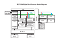
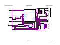
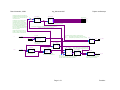
EE/CS 52 Digital Oscilloscope Block Diagram
FPGA
Clock Logic
Reset Logic
Address
Data
Control
NIOS CPU
Keypad
Debouncer
VRAM/LCD
Controller
Analog
FIFO
Analog
Control Block
Buffers
Chip Select
Logic
Interrupt
Controller
SRAM
ROM
VRAM
LCD
PIOs
UART
Buffers
Serial
ADC
Keypad
1
2
3
4
5
6
VEE (-12V)
D
APEX_J3
VCC3.3
VCC3.3
TDO
xTDO
TMS
TCK
TDI
xTDI
GND
GND
nWS
nRS
nCS
CS
DEVCLRn
DCLK
CLK2
nCE
DEVOE
LOCK
1
2
3
4
5
6
7
8
9
10
11
12
13
14
15
16
17
18
19
20
APEX_J10
Top Left of the Adapter Board
Row 0 Select
Row 1 Select
Row 2 Select
Row 3 Select
A0
A1
A2
A3
12
11
10
9
8
7
6
5
27
26
23
25
4
28
29
3
2
30
1
22
24
31
A4
A5
A6
A7
A8
A9
A10
A11
A12
A13
A14
A15
A16
A17
A18
R1
Res2
10K
R2
Res2
10K
A0
A1
A2
A3
A4
A5
A6
A7
A8
A9
A10
A11
A12
A13
A14
A15
A16
A17
A18
DQ1
DQ2
DQ3
DQ4
DQ5
DQ6
DQ7
DQ8
13
14
15
17
18
19
20
21
D0
D1
D2
D3
D4
D5
D6
D7
CE
OE
WE
Am29F040-120
ROM
A0
A1
A2
A3
A4
A5
A6
A7
A8
A9
A10
A11
A12
A13
A14
10
9
8
7
6
5
4
3
25
24
21
23
2
26
1
22
27
20
A0
A1
A2
A3
A4
A5
A6
A7
A8
A9
A10
A11
A12
A13
A14
D0
D1
D2
D3
D4
D5
D6
D7
11
12
13
15
16
17
18
19
D0
D1
D2
D3
D4
D5
D6
D7
OE
WE
CS
W24257A
SRAM
S1
SW-PB
VCC
Reset Circuitry
6
R3
Res1
1K
1
4
3
R4
Res1
1K
WDI
VCC
MR
PFI
WDO
RST
GND
PFO
VCC
2
8
7
5
MAX706SCSA
11
12
13
14
15
1
2
3
4
A0
A1
A2
A3
A4
A5
A6
A7
A8
A9
A10
A11
A12
A13
A14
A15
A16
A17
A18
Column 3
D0
D1
D2
D3
D4
D5
D6
D7
15
14
13
12
11
4
3
2
1
Column 0 Data
Column 1 Data
Column 2 Data
Column 3 Data
J?
50 APEX_J9
GND
49
GND
48
U5OE1
47
U5DIR1
46
DATA7
45
Keypad Conn2
DATA6
Header 10X2A
44
Row 0
DATA0
43
DATA5
42
Row 1
DATA4
41
DATA3
40
Row 2
IO164
39
IO165
38
Row 3
GND
37
KEYPAD4X4
IO166
36
IO167
35
DATA2
34
Keypad debouncing is done in the FPGA
IO170
33
IO171
32
R6 R7 R8 R9
DATA1
31
IO174
30
4.6K 4.6K 4.6K 4.6K
IO175
29
U5DIR2
28
Pull columns low when no key is pressed.
U5OE2
27
CLKUSR
26
RDYnBSY
25
INITDONE
24
IN181
23
GND
22
IN184
21
nCEO
20
TRST
19
IO188
18
IO190
17
U?
IO191
1
7
16
SC WB/WE
IO192
4
15
Only one VRAM chip is used, so SOE is low
DT/OE
IO193
W/IO0
21
14
SOE
IO194
W/IO1
18
13
CAS
IO195
W/IO2
23
8
12
SO3 RAS
IO196
W/IO3
22
11
SO2
GND
3
13
10
SO1
A7
IO197
2
9
9
SO0
A6
IO198
10
8
A5
IO200
11
7
A4
IO201
20
14
6
W/IO3 A3
IO202
19
15
5
W/IO2 A2
IO203
6
16
4
W/IO1 A1
IO204
5
17
3
W/IO0 A0
IO205
2
VCC3.3
1
41264
VCC3.3
J?
R5 20 APEX_J2
GND
Res3 19
GND
U1B
100K 18
nCONFIG
17
NC4
16
3
14
T2IN
NC3
Tx
DY
15
IO22
14
TX 2
IO21
U2B
13
145406
IO20
12
J?
IO19
11
5
3
14
IO18
Tx
10
9
DY
IO17
U1A
9
4
TX 1
T1IN
GND
8
DA
8
145406
NC2
7
3
4
15
NC1
Rx
6
RY
RA
7
IO15
5
2
DA
RX 2
IO14
4
6
145406
IO13
U2A
3
1
IO9
2
IO7
1
2
15
D Connector 9
R2OUT
IO6
Rx
RY
RA
R1OUT
RX 1
APEX_J4
145406
Column 2
512k * 8 Bit ROM
Column 1
Column 0
Keypad Conn1
Header 10X2A
WDI, WDO, and PFO are left floating as allowed by datasheet.
Keypad Col on Buffer 10.2
43 Ohm
A
Buffer 5.1 is Disabled
R10
LED1
VCC5
VCC5
VCC5
IO113
IO115
IO116
IO117
IO120
IO122
IO123
IO134
uIO162
IO135
IO139
IO140
IO144
IO151
IO152
IO155
IO159
B
Buffer 5.2 is Disabled
LCD Sense
20
19
18
17
16
15
14
13
12
11
10
9
8
7
6
5
4
3
2
1
VRAM data bus is on U4.1
Start Frame (DI)
Display Enable
AC Drive Signal (FR)
LAT / Y Shift Clock
DS?
C
VRAM Address Bus on U4.2
YSCL/LP
ECL
XSCL
Top Right of the Adapter Board
1
GND
2
IO34
3
IO37
4
IO38
5
IO40
6
IO41
7
IO42
8
NC5
9
NC6
10
GND
11
IO44
12
IO45
13
IO46
14
IO49
15
IO50
16
IO51
17
NC7
18
NC8
19
GND
20
GND
J?
1
APEX_J5
VCC3.3
2
VCC3.3
3
IO58
4
IO59
5
IO60
6
IO61
7
IO62
8
IO63
9
IO65
10
IO66
11
GND
12
IO67
13
IO68
14
IO69
15
IO70
16
IO71
17
IO72
18
IO73
19
IO74
20
GND
21
IN77
22
GND
23
IN81
24
GND
25
nSTATUS
26
GND
27
CONFDONE
28
GND
29
IO89
30
IO90
31
IO91
32
IO92
33
IO93
34
IO94
35
IO96
36
IO97
37
GND
38
IO98
39
IO99
40
IO100
41
IO101
42
IO102
43
IO103
44
IO104
45
IO106
46
VCC5
47
VCC5
48
GND
49
CLK1
50
VCC5
J?
LED & Ke ypad Row on Buffer 10.1
11
12
13
14
15
16
17
18
1
2
3
4
5
6
7
8
9
10
D0
D1
D2
D3
Display Connector
Header 10X2A
Serial RX on Buffer 8.1 Serial TX on Buf fer 8.2
C
Address Lines on Buffer 7.1 and 7.2
Address and CS on Buffer 6.2
B
Data on Buffer 6.1
VRAM Ctl Lines on Buffer 9.2
A
OE/WE and LCD Ctl Lines on Buffer 9.1
VDD (5V)
D
Title
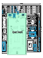
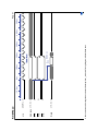
EE52 Digital Oscilloscope Protoboard
Size
Number
Revision
1.0
B
Date:
File:
1
2
3
4
5
11/19/2008
Sheet of
C:\Documents and Settings\..\protoboard.schdoc
Drawn By: Julian Panetta
6
Keypad Conn
Power
Conn.
Power
Conn.
LED
Reset
Key
Reset
Power
Jack
JTAG
VRAM
Apex Board
SRAM
ROM
Capacitors
Display Connector
DB-9
RS-232
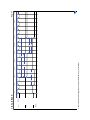
Timing Diagrams
o VRAM
Timing Specifications
Read, Write, Refresh, Data Transfer
o LCD
Timing Specifications (1180F, 1190)
LCD Signals
o SRAM
Read, Write
o Rom
Read
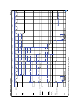
50ns
25ns
10ns
120ns
10ns
100ns
40ns
35ns
20ns
95ns
AR
t
t
t
t
t
t
t
tCP
t
tCRP
t
tCSR
t
tCWL
t
tDHH
t
tDHS
Column address setup time
Row address setup time
Access time from CAS
Column address hold time
CAS pulse width
DT low hold time after RAS low
CAS before RAS refresh hold time
CAS precharge time (page cycle only)
CAS precharge time (nonpage cycle)
CAS high to RAS low precharge time
CAS hold time
CAS before RAS refresh setup time
CAS to WE delay
Write command to CAS lead time
Data-in hold time
DT high hold time
Data-in hold time after RAS low
DT high setup time
DHR
DH
CWD
CSH
CPN
CHR
CDH
CAS
CAH
CAC
ASR
ASC
t
Column address hold time after RAS
low
0
25ns
40ns
60ns
20ns
0ns
0ns
80ns
SYMBOL MIN
DESCRIPTION
VRAM Timing Specifications
60ns
MAX
Page 2
10ns
20ns
10ns
15ns
120ns
220ns
25ns
t
tDTH
t
t
t
t
t
t
t
t
tPC
t
tRAH
t
tRC
t
tRCH
DT high to CAS high delay
DT high hold time after RAS high
DT high to RAS high delay
OE pulse width
Access time from OE
OE to data-in setup delay
OE hold time after WE low
OE to RAS inactive setup time
Output disable time from OE high
Output disable time from CAS high
Page cycle time
Access time from RAS
Row address hold time
RAS pulse width
Random read or write cycle time
RAS to CAS delay time
Read command hold time after CAS
high
RCD
RAS
RAC
OFF
OEZ
OES
OEH
OED
OEA
OE
DTR
DTC
0
120ns
0
0
10ns
30ns
35ns
35ns
0
tDS
Data-in setup time
DLS
t
0
SYMBOL MIN
DT low setup time
DESCRIPTION
VRAM Timing Specifications continued...
60ns
10000ns
120ns
30ns
30ns
30ns
MAX
Page 3
10ns
10ns
tRDH
t
t
t
t
t
t
tRWD
t
t
t
t
t
t
tSDD
t
tSOA
t
DT low hold time after RAS low (serial
port active)
Refresh interval
RAS precharge time
RAS high to CAS low precharge time
Read command hold after RAS high
RAS hold time
Read-write/read-modify-write cycle time
RAS to WE delay
to be defined
Write command to RAS lead time
SC pulse width
Serial output access time from SC
Serial clock cycle time
SC precharge time
SC high to DT high delay
SC low hold time after DT high
Serial output access time from SOE
SOE pulse width
SOE
SDH
SCL
SCC
SCA
SCH
RWL
RWC
RSH
RRH
RPC
RP
REF
15ns
10ns
40ns
10ns
40ns
160ns
300ns
60ns
20ns
0
90ns
100ns
0
t
Read command setup time
RCS
SYMBOL MIN
DESCRIPTION
VRAM Timing Specifications continued...
35ns
50000ns
40ns
4ns
MAX
Page 4
50ns
15ns
0
3ns
95ns
0
20ns
35ns
t
tSOZ
t
t
t
t
tWCR
t
tWH
t
tWS
t
SOE precharge time
Serial output disable time from SOE
high
Rise and fall transition time
Write-per-bit hold time
Write-per-bit setup time
Write command hold time
Write command hold time after RAS low
Write command setup time
Write bit selection hold time
Write command pulse width
Write bit selection setup time
Actual RAS to CAS delay
ual
RCD_Ac t
WP
WCS
WCH
WBS
WBH
T
SOP
100
0
35ns
0
20ns
100
30ns
5ns
tSOO
10ns
SOE low to serial output setup delay
SOH
t
Serial output hold time after SC high
MAX
SYMBOL MIN
DESCRIPTION
VRAM Timing Specifications continued...
Page 5
O
CAS
O
DT/OE
W /IO
tASR
tCRP
DHS
t
Row
0ns
50ns
tRAH
tRAC
tRCS
Column
DHH
t
tAR
tASC
tRCD_Actual
tCPN
100ns
tCSH
tRAS
tCAH
CAC
t
tOEA
150ns
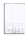
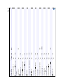
C:\Documents and Settings\Administrator\Desktop\vram_read.tdml
i
O
i
O
WB/WE
Address [15..0] O
O
20MHz O
RAS
clk
vram_read
Read Data
OE
t
tOES
tCAS
tRSH
tRC
200ns
tOEZ
OFF
t
250ns
RCH
tRRH
t
tRP
300ns
350ns
400ns
450ns
500ns
Page 1
O
CAS
O
O
DT/OE
Wi /IOi
-50ns
WBS
tASR
CRP
t
50ns
Write Mask Valid
tWS
tDHS
t
Row
0ns
tWH
tWBH
tRAH
tCPN
tASC
tAR
WCR
t
tCSH
RAS
t
150ns
DHR
t
tDS
Input Data Valid
tDHH
tWCS
Column
RCD_Actual
t
100ns
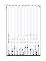
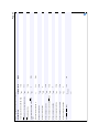
C:\Documents and Settings\Administrator\Desktop\vram_write.tdml
O
WB/WE
Address [15..0] O
O
20MHz O
RAS
clk
vram_write
tDH
tRWL
tCWL
tWP
tCAH
tWCH
tCAS
RSH
t
tRC
200ns
250ns
RP
t
300ns
350ns
400ns
450ns
Page 1
O
O
CAS
Wi /IOi
0ns
50ns
tCSR
100ns
tCHR
150ns
tRAS
200ns
C:\Documents and Settings\Administrator\Desktop\vram_refresh.tdml
O
20MHz O
RAS
clk
vram_refresh
tRC
250ns
tRPC
tRP
300ns
350ns
400ns
450ns
500ns
Page 1
DTR
t
tDTC
SDH
t
250ns
DTH
t
tRP
300ns
t
SOH
SOH
t
tCDH
tCAH
tCAS
tRSH
tRC
200ns
t
SDD
t
RDH
t
Column
tASC
tAR
tCSH
tRAS
150ns
SCA
Old Data
tRAH
tRCD_Ac tual
tCPN
100ns
SCA
t
DLS
t
Row
tASR
tCRP
50ns
C:\Documents and Settings\Administrator\Desktop\vram_dt.tdml~
O
SO
O
Wi /IOi
O
O
DT/OE
SC
3.333333MHz
O
I
WB/WE
[7..0]
O
CAS
Address
O
20MHz O
RAS
clk
0ns
VRAM Data Transfer
New Data
350ns
400ns
450ns
500ns
Page 1
Shift clock "L" width
Latch timing
t
Latch pulse data setup
time
t
Permissible frame signal
delay
t
DFR
Latch pulse data hold
time
tLDH
LDS
Latch hold time
tLH
LT
Latch pulse "L" width
Latch pulse "H" width
Enable clock setup time
Enable clock delay time
Enable data hold time
Enable data setup time
Enable clock "L" width
tWLPL
WLPH
t
ECS
t
EDR
t
EDH
t
EDS
t
WECL
t
WECH
t
Enable clock "H" width
Data hold time
t
DH
Data setup time
tDS
WCLL
t
shift clock cycle
DESCRIPTION
Shift clock "H" width
DEFINITION
tWCLH
CLC
t
SYMBOL
1180F
-500
50
140
0
100
220
110
70
-10
20
50
100
100
30
50
63
63
166
MIN
500
MAX
NOTES
Page 2
PD
t
SYMBOL
1180F continued...
DEFINITION
Enable output delay
DESCRIPTION
20
MIN
150
MAX
NOTES
Page 3
Latch pulse cycle time
t
Latch pulse "L" width
t
Data output delay time
t
pD
Permissible frame signal
delay
Data shift hold time
Data shift timing
Data hold time
Data setup time
DFR
t
STH
t
ST
t
DH
t
DS
t
WCLL
t
Shift clock "L" time
Shift clock "H" time
t
WCLH
Shift clock cycle time
tCYC
WLL
Latch pulse "H" width
tWLTH
CYL
DEFINITION
SYMBOL
1190
to be defined
to be defined
to be defined
to be defined
to be defined
to be defined
to be defined
to be defined
to be defined
to be defined
to be defined
to be defined
DESCRIPTION
30
-500
125
0
30
70
240
110
400
180
180
400
MIN
170
500
MAX
NOTES
Page 4
O
O
ECL
XSCL
3.333333MHz
O
DT_NOW
0ns
tCLC
200ns
tDS
tWCLH
tEDR
tWECH
tLT
LDS
t
400ns
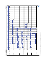
C:\Documents and Settings\Administrator\Desktop\LCD_Timing_Long.tdml
O
DI
I
O
LP/YSCL/LAT
[3..0]
O
FR
Data
20MHz O
clk
LCD Timing
tDH
tWCLL
tECS
WLPH
t
WLTH
t
LDH
t
tLH
800ns
tDH
New frame data
DFR
t
tDS
600ns
1us
1.2us
Page 1
20MHz O
-50ns
0ps
TAA
50ns
TOH
100ns
150ns
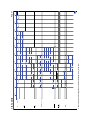
C:\Documents and Settings\Administrator\Desktop\from_windows\Timing Diagrams\SRAM Read.tdml
data_requirement
[15..0] O
O
RD
Data
O
CS
Address [15..0] O
clk
SRAM
200ns
250ns
300ns
Page 1
20MHz O
O
WE
-20ns
0ns
20ns
40ns
60ns
C:\Documents and Settings\Administrator\Desktop\from_windows\Timing Diagrams\SRAM Write.tdml
[15..0] O
O
OE
Data In
O
CS
Address [15..0] O
clk
SRAM Write
80ns
100ns
120ns
Page 1
20MHz O
O
OE
-100ns
0ns
100ns
tACC (120ns)
200ns
300ns
C:\Documents and Settings\Administrator\Desktop\from_windows\Timing Diagrams\ROM Read.tdml
[15..0] O
O
WE
Data
O
CE
Address [15..0] O
clk
ROM Read
400ns
500ns
Page 1
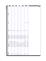
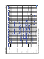
Memory Map
Digital Oscilloscope APEX20K Pin Assignments
To
CLOCK
RESET
U4OE1
U4OE2
U6OE1
U6OE2
U6DIR2
U7DIR1
U7DIR2
U7OE1
U7OE2
U8DIR1
U8DIR2
U8OE1
U8OE2
U9DIR1
U9DIR2
U9OE1
U9OE2
U10OE1
U10OE2
addr[0]
addr[1]
addr[2]
addr[3]
addr[4]
addr[5]
addr[6]
addr[7]
addr[8]
addr[9]
addr[10]
addr[11]
addr[12]
addr[13]
addr[14]
addr[15]
addr[16]
addr[17]
addr[18]
data[0]
data[1]
data[2]
data[3]
data[4]
data[5]
data[6]
Location
PIN_27
PIN_142
PIN_187
PIN_206
PIN_57
PIN_84
PIN_85
PIN_87
PIN_108
PIN_88
PIN_107
PIN_2
PIN_31
PIN_5
PIN_30
PIN_32
PIN_55
PIN_33
PIN_54
PIN_112
PIN_158
PIN 71
PIN_71
PIN_72
PIN_73
PIN_74
PIN_89
PIN_90
PIN_91
PIN_92
PIN_93
PIN_94
PIN_96
PIN_97
PIN_98
PIN_99
PIN_100
PIN_101
PIN_102
PIN_103
PIN_104
PIN_58
PIN_59
PIN_60
PIN_61
PIN_62
PIN_63
PIN_65
General Function
Dedicated Clock
Row I/O
Column I/O
Column I/O
Column I/O
Column I/O
Column I/O
Column I/O
Row I/O
Column I/O
Row I/O
Row I/O
Row I/O
Row I/O
Row I/O
Row I/O
Column I/O
Row I/O
Column I/O
Row I/O
Column I/O
Col mn I/O
Column
Column I/O
Column I/O
Column I/O
Column I/O
Column I/O
Column I/O
Column I/O
Column I/O
Column I/O
Column I/O
Column I/O
Column I/O
Column I/O
Column I/O
Column I/O
Column I/O
Column I/O
Column I/O
Column I/O
Column I/O
Column I/O
Column I/O
Column I/O
Column I/O
Column I/O
Special Function
CLK1
nRS
Digital Oscilloscope APEX20K Pin Assignments
data[7]
PIN_66
nCS_RAM PIN_37
nCS_ROM PIN_34
nRD
PIN_67
nWR
PIN_68
U6DIR1
PIN_56
TX1
PIN_17
RX2
PIN_7
keypad_rowPIN_120
keypad_rowPIN_122
keypad_rowPIN_123
keypad_rowPIN_134
keypad_col PIN_140
keypad_col PIN_144
keypad_col PIN_151
keypad_col PIN_152
U10DIR1
PIN_111
U10DIR2
PIN_161
STATUS_LE PIN_117
U4DIR1
PIN_179
U4DIR2
PIN_207
vaddr[0] PIN_44
vaddr[1]
addr[1] PIN_204
PIN 204
vaddr[2] PIN_203
vaddr[3] PIN_202
vaddr[4] PIN_201
vaddr[5] PIN_200
vaddr[6] PIN_198
vaddr[7] PIN_197
vdata[0] PIN_193
vdata[1] PIN_194
vdata[2] PIN_195
vdata[3] PIN_196
nRAS
PIN_45
nCAS
PIN_46
nDTOE
PIN_49
nWBWE
PIN_50
VRAM_SC PIN_51
DI
PIN_38
DisplayEnabPIN_40
FR
PIN_41
LP
PIN_113
ECL
PIN_115
YSCL
PIN_42
Column I/O
Row I/O
Row I/O
Column I/O
Column I/O
Column I/O
Row I/O
Row I/O
Row I/O
Row I/O
Row I/O
Row I/O
Row I/O
Row I/O
Row I/O
Row I/O
Row I/O
Column I/O
Row I/O
Column I/O
Column I/O
Row I/O
Col mn I/O
Column
Column I/O
Column I/O
Column I/O
Column I/O
Column I/O
Column I/O
Column I/O
Column I/O
Column I/O
Column I/O
Row I/O
Row I/O
Row I/O
Row I/O
Row I/O
Row I/O
Row I/O
Row I/O
Row I/O
Row I/O
Row I/O
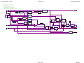
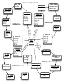
Quartus Design •
•
•
•
•
•
Top Level Design
Analog Control Block
LCD/VRAM Control Block
LCD Signal Generator
Keypad Debouncer
Clock Divider
Date: November , 2008
oscilloscope.bdf
Project: oscilloscope
Control line for the status LED.
Bringing this line high turns on the LED.
OUTPUT
GND
NIOS
clk
reset_n
INPUT
VCC
RESET
Buffer Enables:
Enabled: Buffers 4, 6, 7, 8, 9, 10
System Reset
out_port_from_the_LED_pio
out_port_from_the_analog_control_reset_pio
out_port_from_the_analog_control_settings_data_pio[15..0]
INPUT
VCC
CLOCK
out_port_from_the_analog_control_settings_selector_pio[2..0]
System Clock (20MHz)
in_port_to_the_analog_fifo_data_in_pio[7..0]
GND
OUTPUT
U4OE1
OUTPUT
U4OE2
OUTPUT
U8DIR1
OUTPUT
U6OE1
OUTPUT
U10DIR2
OUTPUT
U6OE2
OUTPUT
U7OE1
OUTPUT
U7OE2
OUTPUT
U8OE1
OUTPUT
U8OE2
OUTPUT
U9OE1
OUTPUT
U9OE2
OUTPUT
U10OE1
OUTPUT
U10OE2
Output: Buffers 6.2 (Address/CS lines), 7 (Address)
8.2 (Serial out), 9.1 (OE,WE,LCD Control lines)
9.2 (VRAM control), 10 (LED, Keypad row)
VCC
4.2 (VRAM address)
in_port_to_the_analog_fifo_empty_pio
in_port_to_the_analog_fifo_full_pio
out_port_from_the_analog_fifo_read_req_pio
Debounce keypresses (with key repeat),
and interrupt the NIOS when one is debounced.
key_debouncer
Keypad row enable lines
INPUT
VCC
keypad_col[3..0]
clk
col[3..0]
Input lines for reading undebounced row
of keypress data from the keypad
row0
row1
row2
row3
key_data[5..0]
key_ready
OUTPUT
keypad_row[0]
OUTPUT
keypad_row[1]
OUTPUT
keypad_row[2]
OUTPUT
keypad_row[3]
OUTPUT
U4DIR2
OUTPUT
U6DIR2
OUTPUT
U7DIR1
OUTPUT
U7DIR2
OUTPUT
U8DIR2
OUTPUT
U9DIR1
OUTPUT
U9DIR2
OUTPUT
U10DIR1
Variable: Buffer 6.1 (Data bus), 4.1 (VRAM data bus)
in_port_to_the_key_ready_pio
OUTPUT
U6DIR1
OUTPUT
U4DIR1
OUTPUT
nCS_RAM
OUTPUT
nCS_ROM
in_port_to_the_keydata_pio[5..0]
WaitRequest_from_the_vram_0
nCS_to_the_ram_0
nCS_to_the_rom_0
nCS_to_the_vram_0
nRS_to_the_vram_0
rom_0_ROMAm29F040B_wait_counter_eq_1
tri_state_bridge_0_address[18..0]
tri_state_bridge_0_data[7..0]
tri_state_bridge_0_readn
tri_state_bridge_0_writen
Debounced key data
IInterrupt line for keypad input
inst13
INPUT
VCC
RX2
STATUS_LED
Buffer Directions (GND = input, VCC = output)
Input: Buffers 8.1 (Serial in), 10.2 (Keypad column)
rxd_to_the_uart_0
Serial input data line for NIOS terminal
RAM and ROM Chip Select Lines
Wait Counter Left Floating
txd_from_the_uart_0
OUTPUT
addr[18..0]
BIDIR
VCC
OUTPUT
data[7..0]
OUTPUT
nWR
OUTPUT
TX1
nRD
inst
Generate signals to control the VRAM and
the LCD, and provide an interface between
the Avalon bus and the VRAM's bus.
LCD_VRAM_Block
8-bit Input from the ADC
lpm_constant7
0
inst6
8
The analog input hardware is not constructed,
so take the input to be a constant zero.
ANALOG_RESET
ADC_DATA[7..0]
SETTING_SELECTOR[2..0]
SETTING_DATA[15..0]
CLK
ADDR[18..0]
nWR
nRD
nCS
nRS
clk
Store ADC samples until software
can read and process them.
inst16
lpm_fifo0
SAMPLE_DATA[7..0]
SAMPLE_REQ
SAMPLE_CLK
analog
When requested, sample data from the ADC at a specified sample rate.
data[7..0]
q[7..0]
wrreq
rdreq
full
empty
clock
sclr
8 bits x 16 words
inst15
DATA
vdata[3..0]
vaddr[7..0]
nCAS
nRAS
nWBWE
nDTOE
DisplayEnable
XSCL
ECL
YSCL
LP
DI
FR
WaitReq
VRAM Ctl/ Bus, LCD Signal Lines
BIDIR
VCC
OUTPUT
vdata[3..0]
OUTPUT
nCAS
OUTPUT
nRAS
OUTPUT
nWBWE
OUTPUT
nDTOE
OUTPUT
DisplayEnable
Drive high to power LCD OUTPUT
vaddr[7..0]
VRAM_SC
OUTPUT
ECL
OUTPUT
YSCL
OUTPUT
LP
OUTPUT
DI
OUTPUT
FR
inst8
System Clock (20MHz)
Page 1 of 1
Revision:
Date: November , 2008
analog.bdf
Analog Control Block
Samples data from the ADC at a specified rate after a set delay
following a trigger event (defined by a configurable level and slope)
The settings are altered by first selecting the desired setting by placing
a 3-bit identifier on the selector line:
1 == Sample rate, 2 == Trigger delay, 3 == Trigger level, 4 == Trigger slope
Then the value for that setting is placed on the SETTING_DATA line.
Once the setting is made, the setting can be deselected by writing the identifier 0
or by selecting another setting to change.
This control block interacts with the FIFO, storing sample data on SAMPLE_CLK's rising edge by
requesting that the FIFO latch in data from the SAMPlE_DATA output using its SAMPLE_REQ line.
clock_divider
INPUT
VCC
System clock (20MHz)
lpm_clshift2
INPUT
VCC
lpm_constant3
Value to be used for the selected setting.
1
inst16
INPUT
VCC
DFF
data[15..0]
clock
enable
result[15..0]
LOGICAL left shift
inst10
clk_in
scale_factor[31..0]
combine_16_16
OUTPUT
clk_out
a[15..0]
c[31..0]
inst17
b[15..0]
Create a sample clock based on the selected
sampling rate.
Put the sample rate clock divider value
in the low 16 bits of the clock divider input
lpm_dff3
DFF
data[15..0]
clock
enable
eq1
eq2
eq3
eq4
q[15..0]
inst6
lpm_constant3
1
inst15
data[7..0]
distance
low[7..0]
high[7..0]
lpm_compare9
lpm_dff2
unsigned compare
DFF
LOGICAL left shift
inst8
data[7..0]
clock
enable
split
a[15..0]
Delay until the specified number of
sample clocks have passed.
Latch in trigger delay.
result[7..0]
Trigger level is 7-bit, while the ADC output is 8-bit. Multiply
level by 2 to distribute levels
evenly throughout 8-bit domain
lpm_compare7
aeb
dataa[15..0]
ageb
datab[15..0]
alb
up counter
clock
q[7..0]
inst5
q[15..0]
cnt_en
inst24
Incoming data from the ADC
inst4
8
8
Texas Instrument's TLC5510 ADC
returns 255 for the lowest voltage and
0 for the highest; so input must be inverted.
zero <==> + slope
nonzero <==> - slope
inst14in trigger delay.
Latch
Latch in trigger slope
dataa[7..0]
datab[7..0]
q
a = trigger level
b = signal level
aeb
agb
inst18
agb <==> signal < trigger
aeb <==> signal == trigger
1
Glen George's trigger
state machine. Triggers
on a specified slope event.
TS
6
NOT
inst
Signal to reset the triggering mechanism
and all the counters use for delay/sampling.
('1' == Reset, '0' == Don't Reset)
16
dataa[15..0]
datab[15..0]
DFF
data
clock
aeb
inst25
lpm_dff5
lpm_constant3
1
inst22
inst30
AND3
DFF
data
clock
enable
NOT
q
inst9
Sample 640 samples
clk
Reset
inst26
TrigEvent
TEQ
INPUT
VCC
lpm_dff7
compare
lpm_constant4
inst2
scoptrig_explicit
TLT
ANALOG_RESET
Stop sampling after 640 samples are taken
until a reset occurs (regardless of new trigger events)
lpm_compare10
OUTPUT
SAMPLE_REQ
OUTPUT
SAMPLE_DATA[7..0]
q
inst33
has_trigger
aclr
lpm_inv0
INPUT
VCC
Only reset trigger delay counter on
first trigger event since reset
unsigned compare
inst3
inst12
data
clock
enable
AND2
Only the low 7 bits are needed for trigger level/slope
lpm_compare8
DFF
aneb
q[15..0]
clock
cnt_en
inst19
Latch in trigger level.
lpm_dff4
dataa[7..0]
datab[]=0
sclr
inst20
compare
inst11
lpm_counter6
up counter
lpm_counter5
aclr
inst1
inst13
lpm_clshift1
1: Set sample rate
2: Set trigger delay
3: Set trigger level
4: Set trigger slope
ADC_DATA[7..0]
SAMPLE_CLK
16
inst28
Latch in sample rate.
lpm_decode1
data[2..0]
q[15..0]
inst7
Sample rate input is a multiplier of a 100ns
period, not the 50ns period of our 20MHz
system clock. It must therefore be multiplied by 2.
Index of the setting to be altered
0
inst29
lpm_constant6
SETTING_SELECTOR[2..0]
data[15..0]
distance
lpm_constant5
aclr
SETTING_DATA[15..0]
lpm_dff3
aclr
CLK
Project: oscilloscope
inst21
Trigger sets has_trigger until it is cleared by ANALOG_RESET
(Must be on the same clock as the trigger, not the sample clock!)
inst27
clock
data[7..0]
q[7..0]
DFF
lpm_dff6
Page 1 of 1
Revision:
Date: November , 2008
LCD_VRAM_Block.bdf
LCD/VRAM Block
Implements reads, writes, data transfers, and refreshes
for the VRAM using a finite state machine implemented in VHDL.
Generates the signals needed to drive the LCD using
a block design file with counters and comparators.
ADDR[18..0]
nWR
nRD
nCS
INPUT
VCC
INPUT
VCC
INPUT
VCC
State machine implementing VRAM cycles.
vram_controller_lut
VRAM Control Lines:
addr[18..0]
INPUT
VCC
VRAM Chip Select
vdata[3..0]
nRD
vaddr[7..0]
DATA
OUTPUT
vaddr[7..0]
vdata[3..0]
nCAS
OUTPUT
nCAS
nCS
nRAS
OUTPUT
nRAS
nWBWE
OUTPUT
nWBWE
nDTOE
OUTPUT
nDTOE
nRS
VRAM / LCD Rest
BIDIR
VCC
OUTPUT
clk
DT_SOON
INPUT
VCC
data[7..0]
nWR
DT_NOW
nRS
Project: oscilloscope
WR
DT_ROW[7..0]
inst
LCD Control Lines:
OUTPUT
clk
INPUT
VCC
nRS
clk
System Clock (20 MHz)
DisplayEnable
(Display enabled when no reset is occuring)
lcd_signal_generator
XSCL
ECL
DT_SOON
DT_NOW
LP
DI
FR
RADDR[7..0]
OUTPUT
XSCL
OUTPUT
ECL
OUTPUT
YSCL
OUTPUT
LP
OUTPUT
DI
OUTPUT
FR
Avalon Bus Ctl Line (Wait Request)
inst1
OUTPUT
WaitReq
Collection of counters that implement pulses to be sent to the LCD
and computes the address of the row the VRAM needs to transfer
into its serial shift register.
Page 1 of 1
Revision:
Date: November , 2008
XSCL has a period of 6 clocks
XSCLCompare
Make sure all signals change on system clock edges
and prevent glitching with flip-flops.
unsigned compare
LCDSignalFlipFlop
clock
q[2..0]
dataa[2..0]
datab[]=3
ECL is high for clocks 2 to
9 at the start of its period.
inst12
ECL has a period of 96 clocks
(Occurs once every 16 XSCLs)
inst7
AND2
LCDSignalFlipFlop
inst10
data
clock
unsigned compare
dataa[6..0]
datab[]=10
ECL
OUTPUT
DT_SOON
OUTPUT
DT_NOW
OUTPUT
LP
OUTPUT
DI
OUTPUT
FR
OUTPUT
RADDR[7..0]
DT_SOON is high from clock 950 in one
(this is a very conservative interval.)
unsigned compare
clock
OUTPUT
SOONCompareLow period to clock 8 in the next.
dataa[9..0]
ageb
datab[]=950
DT_NOW is high for clocks
3 to7 at its period beginning
up counter
modulus 960
q
inst48
alb
inst32
sclr
XSCL
DFF
ECLCompareHigh
inst
DTCounter
OUTPUT
ageb
inst31
q[6..0]
DT has a period of 960 clocks
(Occurs once every 10 ECLs)
q
inst47
unsigned compare
dataa[6..0]
datab[]=2
up counter
modulus 96
clock
data
clock
ECLCompareLow
ECLCounter
sclr
DFF
alb
OR2
LCDSignalFlipFlop
inst23
data
clock
DFF
inst33
SOONCompareHigh
q
inst49
unsigned compare
NOWCompareLow
unsigned compare
q[9..0]
dataa[9..0]
datab[]=5
inst2
dataa[9..0]
datab[]=8
ageb
alb
inst35
inst41
AND2
LCDSignalFlipFlop
inst22
data
clock
DFF
NOWCompareHigh
unsigned compare
dataa[9..0]
datab[]=8
q
inst50
alb
NOT
Must be made active high
inst37
INPUT
VCC
sclr
inst6
Row increment "clock"
clk
System clock (20MHz)
up counter
modulus 6
inst42
LP has a period of 1920 clocks
(Occurs once every 20 ECLs)
LPCompareLow
unsigned compare
LPCounter
up counter
modulus 1920
sclr
LP is high from clocks 6 to 13
at the start of its period
dataa[10..0]
ageb
datab[]=6
inst43
clock
AND2
LCDSignalFlipFlop
inst18
data
clock
DFF
q[10..0]
LPCompareHigh
inst3
unsigned compare
dataa[10..0]
datab[]=14
q
inst51
alb
inst44
DICompareLow
DI has a period of 192000 clocks
(Occurs once very 100 LPs)
unsigned compare
DICounter
sclr
DI is high for clocks 12 to 17
at the start of its period
dataa[17..0]
ageb
datab[]=12
up counter
modulus 192000
inst45
AND2
LCDSignalFlipFlop
inst21
data
clock
DFF
clock
DICompareHigh
q[17..0]
unsigned compare
inst4
dataa[17..0]
datab[]=18
q
inst52
alb
inst46
FRToggle
NOT
TFF
clock
q
inst36
Toggle FR on falling
edge of DI
LCDSignalFlipFlop
DFF
data
clock
q
inst53
inst54
There are 200 rows to transfer to the LCD in total.
Move to the next row each LP (so the inverted LP signal is used as a clock)
RowCounter
clock
up counter
modulus 200
Row_Decoder
RowAddressFlipFlop
DFF
q[7..0]
RowCounter[7..0]
ROW_ADDR[7..0]
aclr
nRS
Signal to clear (reset) components
XSCL is high for 3 clocks and
low for 3 clocks.
XSCLCounter
NOT
INPUT
VCC
Project: oscilloscope
aclr
LCD Signal Generator
Generates the timing signals to be sent to the LCD
and the row address used during a VRAM Data Transfer
See the LCD timing diagram for the timings that this
design implements.
Inputs:
nRS - Active low reset signal
clk - System clock, assumed to be 20MHz
lcd_signal_generator.bdf
inst5
Asynchronous clear is used because the clock
Event will never occur upon reset.
data[7..0]
clock
q[7..0]
inst55
inst1
To make rows of VRAM correspond to physical rows on the LCD
Transfer rows in the order 0, 100, 1, 101, etc.
Page 1 of 1
Row increment "clock"
Revision:
Date: November , 2008
key_debouncer.bdf
This design file implements a keypad debouncer.
The implementation debounces a keypress for 20ms
and repeats a key every subsequent 300ms if the
user continues to hold it.
lpm_counter1
NOT
Project: oscilloscope
lpm_decode0
Row select lines
up counter
clock
inst13
The debouncer supports multiple keypresses
on a single row, but does not respond to
simultaneous kepresses occuring on different
rows. In this case, the first row with a keypress
encountered during row multiplexing is the only
one from which keypresses are debounced.
cnt_en
q[1..0]
data[1..0]
inst7
eq0
eq1
eq2
eq3
OUTPUT
row0
OUTPUT
row1
OUTPUT
row2
OUTPUT
row3
inst
Select keypad row corresponding to given 2-bit address
notDebouncing: row multiplexing counter increments only when we are not debouncing
(when there is no kepress read from the current row)
When a key is debounced, key_ready will pulse
high for 1ms, and the encoded presses can be
read from key_data[6..0].
This debouncer assumes that the clock runs
at 20MHz. If it doesn't, the debounce and key
repeat times will differ from the stated values.
clk
The the 6-bit key output, key_data[5..0], is encoded as follows:
Bits 5 - 4 -- the index of the row from which the presses were read
Bits 0 - 3 -- nibble representing the pressed keys in the row (1 = pressed)
clock_divider
INPUT
VCC
lpm_constant1
20000
inst4
clk_in
scale_factor[31..0]
32
clk_out
combine
a[1..0]
c[5..0]
OUTPUT
key_data[5..0]
OUTPUT
key_ready
b[3..0]
inst2
Divide clock by 20000 so that
it cycles every 1 ms
inst3
lpm_compare2
compare
dataa[3..0]
datab[]=0
aeb
inst5
lpm_dff0
col[3..0]
INPUT
VCC
lpm_compare1
DFF
data[3..0]
clock
q[3..0]
inst10
Poll the current keypad row
once each millisecond.
compare
dataa[3..0]
datab[3..0]
lpm_counter3
Are any keys being held?
sclr
up counter
modulus 300
Key is debounced after 20ms have passed without
the row nibble changing. Key will repeat after being
held for 300ms, since the counter reduces(mod 300)
lpm_compare3
compare
aneb
lpm_dff1
clock
q[8..0]
NOT
inst1
cnt_en
Detect changes in the row nibble,
which will reset the debouncing counter
dataa[8..0]
datab[]=20
inst11
inst6
inst12
debounce_counter only counts when we are debouncing a
key (when the row data read is not zero). The counter resets
every time a value is read that differs from the last read.
Page 1 of 1
DFF
aeb
data
clock
q
inst8
Prevent key_ready from glitching when it
changes due to combinational logic since it
needs to be used as an interrupt line.
Revision:
Date: November , 2008
clock_divider.bdf
Project: oscilloscope
Clock Divider
Divides clk_in by scale_factor, generating a new clock on clk_out.
Known issues: if scale_factor is odd, the divided clock cycle will
occur in (scale_factor - 1) ticks (rounds down to nearest even
integer). A scale_factor of 1 is not allowed, as it will cause an
overflow in the computation of (scale_factor / 2) - 1.
clk_in
Make counter reduce mod (scale_factor / 2) - 1
lpm_counter4
up counter
sclr
INPUT
VCC
q[31..0]
clock
lpm_compare5
inst
unsigned compare
Toggle clock output every (scale_factor / 2)
counts, so that an entire output clock cycle
occurs in scale_factor counts.
lpm_add_sub0
lpm_clshift0
scale_factor[31..0]
INPUT
VCC
lpm_constant0
1
inst3
data[31..0]
distance
result[31..0]
LOGICAL right shift
inst2
Divide scale_factor by two to determine the number
of counts the divided clock should be high, and how
many counts it should be low.
dataa[31..0]
1
A
A-B
result[31..0]
lpm_tff0
dataa[31..0]
ageb
datab[31..0]
inst4
B
TFF
data
clock
q
OUTPUT
clk_out
inst5
inst6
We want (scale_factor / 2) distinct counter
values, so we count up to (scale_factor / 2) - 1
Page 1 of 1
Revision:
VHDL •
•
VRAM Controller State Machine
o State machine diagram
o vram_controller_lut.vhd
Miscellaneous Helper Blocks
o split.vhd
o combine.vhd
o combine_16_16.vhd
READ_TWO
nRAS low
READ_THREE
Assert Col Addr
READ_ONE
Assert Row Addr
nDT High
nCAS high
nWE High
WRITE_ONE
Assert Row Addr
Assert Write Mask
nCAS high
nWB low
nDT high
VRAM Read Cycle
w,
nRD lo low
ON
DT_SO
READ_FIVE
Transfer Data
WR low
READ_SIX
nRAS high
nCAS high
nOE high
WR high
igh
W
DT ONE
Assert Row Addr
nDT Low
nCAS high
DT_TWO
nRAS low
WRITE_THREE
Assert Input Data
Assert Col Addr
WRITE_TWO
nRAS low
h
O
_N
DT
WRITE_FOUR
nCAS low
VRAM Write Cycle
WRITE_FIVE
WAIT
DT nWR
_S
OO low,
N
low
READ_FOUR
nCAS low
nOE low
Actions executed upon state entry.
IDLE
WR High
DT
_S
nC OON
Sh
l
igh ow
WRITE_SIX
nRAS high
nCAS high
nWB high
WR low
REFRESH_ONE
nCAS low
DT_SIX
nRAS high
nCAS high
REFRESH_TWO
nRAS low
VRAM Refresh Cycle
DT_THREE
Assert Col Addr
VRAM Data Transfer Cycle
DT_FOUR
nCAS low
DT_FIVE
nDT high
REFRESH_FIVE
nRAS high
REFRESH_THREE
nCAS high
REFRESH_FOUR
WAIT
vram_controller_lut.vhd
Page 1
---------------------------------------------------------------------------------- Oscilloscope VRAM Controller
--- This VHDL file implements a controller for the NEC uPD41264-12 VRAM chip.
-- The controller is implemeted using a state machine whose transitions are
-- a function of the input lines. Output signals change upon transition to
-- a new state, and their values are looked up in a table indexed by current
-- state number.
--- The controller uses a wait request line to halt the NIOS cpu until it is
-- able to complete a read or write, since a refresh cycle or data transfer
-- cycle could delay read/write cycles an amount unpredictable to the Avalon
-- Tristate Bus.
--- See the state diagram for a visual overview of the state machine.
-- Inputs and outputs are enumerated and described in the port section below.
--- Revision History:
-10/23/08
Julian Panetta Initial Revision
-11/16/08
Julian Panetta Reformatted to fit within 80 chracters wide
--------------------------------------------------------------------------------Library ieee;
use ieee.std_logic_1164.all;
use ieee.std_logic_unsigned.all;
use ieee.numeric_std.all;
entity vram_controller_lut is
port
(
-- 16-bit address input (row & column addresses) with 3 disregarded
-- most significant bits so it interfaces with 19-bit shared Avalon bus
addr
:
in std_logic_vector(18 downto 0);
-- 8-bit data bus (data / writemask nibbles)
data
:
inout std_logic_vector(7 downto 0);
-- Write enable
nWR
:
in std_logic;
-- Output enable
nRD
:
in std_logic;
-- System clock (Assumed to be 20MHz)
clk
:
in std_logic;
-- Chip select
nCS
:
in std_logic;
-- Data transfer needs to occur before a new cycle can be completed.
-- ('1' == true, '0' == false)
DT_SOON :
in std_logic;
-- Data transfer needs to occur NOW
-- ('1' == true, '0' == false)
DT_NOW :
in std_logic;
-- reset state machine to known, IDLE state
nRS
:
in std_logic;
-- Row address to be used for the data transfer cycle.
-- (The data transfer column is always 0.)
DT_ROW :
in std_logic_vector(7 downto 0);
vram_controller_lut.vhd
Page 2
-- 4-bit data bus to VRAM
vdata
:
inout std_logic_vector(3 downto 0);
-- 8-bit address bus out to VRAM
vaddr
:
out std_logic_vector(7 downto 0);
-- CAS signal to VRAM
nCAS
:
out std_logic;
-- RAS signal to VRAM
nRAS
:
out std_logic;
-- nWB/nWE signal to VRAM
nWBWE
:
out std_logic;
-- nDT/nOE signal to VRAM
nDTOE
:
out std_logic;
-- Wait request signal for NIOS
WR
:
out std_logic
);
end vram_controller_lut;
architecture Moore_machine of vram_controller_lut
constant
IDLE
:
integer range
-- VRAM Read Cycle States
constant
READ_ONE
:
integer range
constant
READ_TWO
:
integer range
constant
READ_THREE
:
integer range
constant
READ_FOUR
:
integer range
constant
READ_FIVE
:
integer range
constant
READ_SIX
:
integer range
-- VRAM Write Cycle States
constant
WRITE_ONE
:
integer range
constant
WRITE_TWO
:
integer range
constant
WRITE_THREE
:
integer range
constant
WRITE_FOUR
:
integer range
integer range
constant
WRITE_FIVE
:
constant
WRITE_SIX
:
integer range
-- VRAM Refresh Cycle States
constant
REFRESH_ONE
:
integer range
constant
REFRESH_TWO
:
integer range
constant
REFRESH_THREE
:
integer range
constant
REFRESH_FOUR
:
integer range
constant
REFRESH_FIVE
:
integer range
-- VRAM Data Transfer Cycle States
constant
DTRAN_ONE
:
integer range
constant
DTRAN_TWO
:
integer range
constant
DTRAN_THREE
:
integer range
constant
DTRAN_FOUR
:
integer range
constant
DTRAN_FIVE
:
integer range
constant
DTRAN_SIX
:
integer range
is
0 to 23 := 0;
0
0
0
0
0
0
to
to
to
to
to
to
23
23
23
23
23
23
:=
:=
:=
:=
:=
:=
1;
2;
3;
4;
5;
6;
0
0
0
0
0
0
to
to
to
to
to
to
23
23
23
23
23
23
:=
:=
:=
:=
:=
:=
7;
8;
9;
10;
11;
12;
0
0
0
0
0
to
to
to
to
to
23
23
23
23
23
:=
:=
:=
:=
:=
13;
14;
15;
16;
17;
0
0
0
0
0
0
to
to
to
to
to
to
23
23
23
23
23
23
:=
:=
:=
:=
:=
:=
18;
19;
20;
21;
22;
23;
-- LUT for control line ouputs. 0 => nRAS, 1 => nCAS, 2 => nWBWE, 3 => nDTOE, 4 =>
WR
type TABLE is array(0 to 23) of std_logic_vector(4 downto 0);
constant
OUTPUT_BITS
:
TABLE := (
-- IDLE control line values
"11111",
-- READ_* control line values
"11111", "11110", "11110", "10100", "00100", "11111",
vram_controller_lut.vhd
Page 3
-- WRITE_* control line values
"11011", "11010", "11010", "11000", "11000", "01111",
-- REFRESH_* control line values
"11101", "11100", "11100", "11100", "11111",
-- DTRAN_* control line values
"10111", "10110", "10110", "10100", "11100", "11111");
signal
CurrentState
:
integer range 0 to 23;
-- current state
signal
NextState
:
integer range 0 to 23;
-- next state
begin
-- Compute the next state (function of current state and inputs) using
-- concurrent statements
NextState <=
-- Transitions to IDLE
when
(nRS = '0')
IDLE
else
IDLE
when
(CurrentState = READ_SIX or
CurrentState = WRITE_SIX or CurrentState = REFRESH_FIVE or
CurrentState = DTRAN_SIX)
-- Idle State transitions
else
READ_ONE
when
else
WRITE_ONE
when
else
REFRESH_ONE when
else
DTRAN_ONE
when
else
IDLE
when
-- Movement Within Cycles
else
CurrentState + 1;
(CurrentState = IDLE and
DT_SOON = '0' and nCS =
(CurrentState = IDLE and
DT_SOON = '0' and nCS =
(CurrentState = IDLE and
DT_SOON = '0')
(CurrentState = IDLE and
(CurrentState = IDLE)
nRD = '0' and
'0')
nWR = '0' and
'0')
nCS = '1' and
DT_NOW = '1')
-- Upon transition into the new state, update the contol line values
-- using the output lookup table.
output_computation : process (CurrentState)
begin
-- Look up and set control line values for the current state
nRAS
<= OUTPUT_BITS(CurrentState)(0);
nCAS
<= OUTPUT_BITS(CurrentState)(1);
nWBWE
<= OUTPUT_BITS(CurrentState)(2);
nDTOE
<= OUTPUT_BITS(CurrentState)(3);
WR
<= OUTPUT_BITS(CurrentState)(4);
-- VRAM address line access
-- Assert row address for the first and second read and write states.
if (CurrentState = READ_ONE or CurrentState = WRITE_ONE or
CurrentState = READ_TWO or CurrentState = WRITE_TWO) then
vaddr
<= addr(15 downto 8);
else
-- Assert col address for the third/fourth read and write states.
if (CurrentState = READ_THREE or CurrentState = READ_FOUR or
CurrentState = WRITE_THREE or CurrentState = WRITE_FOUR) then
vaddr
<= addr(7 downto 0);
else
-- Assert DT row address for the first and second DT states.
if (CurrentState = DTRAN_ONE or CurrentState = DTRAN_TWO) then
vaddr
<= DT_ROW;
else
-- Output zero addess in all other states.
vaddr
<= "00000000";
end if;
end if;
end if;
vram_controller_lut.vhd
Page 4
-- VRAM data bus access
-- Transfer VRAM data to Avalon Bus for the fifth read state.
if (CurrentState = READ_FIVE) then
data
<= "0000" & vdata;
else
-- Assert write mask for the first and second write state.
if (CurrentState = WRITE_ONE or CurrentState = WRITE_TWO) then
vdata
<= data(7 downto 4);
else
-- Assert graphics nibble for the third and fourth write state.
if (CurrentState = WRITE_THREE or
CurrentState = WRITE_FOUR) then
vdata
<= data(3 downto 0);
else
-- In all other states, the Avalon data bus and the VRAM
-- data bus should be high impedance.
vdata <= "ZZZZ";
data <= "ZZZZZZZZ";
end if;
end if;
end if;
end process output_computation;
-- Make actual transition to the new state on rising clock edge
make_transition : process (clk)
begin
if clk = '1' then
-- Only change on the rising clock edge
CurrentState <= NextState;
-- Transition to the new state
end if;
end process;
end Moore_machine;
Date: November , 2008
split.vhd
Project: oscilloscope
-------------------------------------------------------------------------------- Split
--- Splits the 16-bit input bits read from port a evenly into the 8 LSBs (place
d
-- on "low" ouptut line) and the 8 MSBs (placed on "high" output line).
--- Revision History:
-09/05/08
Julian Panetta Initial Revision
-----------------------------------------------------------------------------Library ieee;
use ieee.std_logic_1164.all;
entity split is
port
(
a
:
low
:
high
:
);
end split;
in std_logic_vector(15 downto 0);
out std_logic_vector(7 downto 0);
out std_logic_vector(7 downto 0)
architecture
dataflow
of
begin
low <= a(7 downto 0);
high <= a(15 downto 8);
end dataflow;
split
is
Page 1 of 1
Revision:
Date: November , 2008
combine.vhd
Project: oscilloscope
-------------------------------------------------------------------------------- Combine
--- (For use with computing debounced keypress output)
-- Concatenates 2-bit row address read from port a with 4-bit column data read
-- from port b into a 6-bit output placed on port c. The row address is placed
-- in the MSBs of the output and the column address is placed in the LSBs.
------------------------------------------------------------------------------Library ieee;
use ieee.std_logic_1164.all;
entity combine is
port
(
a
:
b
:
c
:
);
end combine;
in std_logic_vector(1 downto 0);
in std_logic_vector(3 downto 0);
out std_logic_vector(5 downto 0)
architecture
dataflow
begin
c <= a & b;
end dataflow;
of
combine is
Page 1 of 1
Revision:
Date: November , 2008
combine_16_16.vhd
Project: oscilloscope
------------------------------------------------------------------------------- Combine 16_16
--- Concatenates two 16-bit inputs (read from ports a and b) into a 32-bit
-- output value placed on port c. the value of port a is placed in the most
-- significant bits of c, and b's value is placed in the least significant
-- bits.
--- Revision History:
-09/05/08
Julian Panetta Initial Revision
----------------------------------------------------------------------------Library ieee;
use ieee.std_logic_1164.all;
entity combine_16_16 is
port
(
a
:
in std_logic_vector(15 downto 0);
b
:
in std_logic_vector(15 downto 0);
c
:
out std_logic_vector(31 downto 0)
);
end combine_16_16;
architecture
dataflow
begin
c <= a & b;
end dataflow;
of
combine_16_16
Page 1 of 1
is
Revision:
Software •
•
Drivers/Initialization (NIOS Assembly)
o start.s
Initializes hardware and calls oscilloscope operating system main
loop.
Global symbols: _start
o keypad.s
Interrupt-driven driver for the keypad
Global symbols: install_key_handler, getkey, key_available
o display.s
Code for drawing on and clearing the LCD
Global symbols: plot_pixel, clear_display
o interrupts.s
Code for initializing interrupts
Global symbols: init_interrupts
o constants.s
Include file holding constants used throughout the NIOS assembly
files listed above.
OS (C)
o stubfuncs.c
Functions emulating hardware not yet implemented
Global symbols: set_sample_rate, set_trigger, set_delay,
start_sample, sample_done
o interfac.h
Include file holding constants used throughout the oscilloscope
operating system.
start.s
Page 1
;;;;;;;;;;;;;;;;;;;;;;;;;;;;;;;;;;;;;;;;;;;;;;;;;;;;;;;;;;;;;;;;;;;;;;;;;;;;;;;;
; File: start.s
; Description:
;
Code run when the NIOS resets. Performs hardware initialization and then
;
branches to Glen George's oscilloscope code.
;
; Input:
Keypresses from the user, analog signal input (not implemented)
; Output:
Output displayed
;
; Known Bugs:
None
; Revision History:
;
11/04/08
Julian Panetta Initial Revision
;
11/17/08
Julian Panetta Added more extensive documentation
;;;;;;;;;;;;;;;;;;;;;;;;;;;;;;;;;;;;;;;;;;;;;;;;;;;;;;;;;;;;;;;;;;;;;;;;;;;;;;;;
.include "excalibur.s"
.include "constants.s"
.text
.global _start
;;;;;;;;;;;;;;;;;;;;;;;;;;;;;;;;;;;;;;;;;;;;;;;;;;;;;;;;;;;;;;;;;;;;;;;;;;;;;;;;
; void _start(void)
;;;;;;;;;;;;;;;;;;;;;;;;;;;;;;;;;;;;;;;;;;;;;;;;;;;;;;;;;;;;;;;;;;;;;;;;;;;;;;;;
; Description:
;
Code located at the NIOS' reset location. Initializes hardware and then
;
runs the oscilloscope OS.
; Operation:
;
- Installs the keypad handler, initialize_interrupts, and forces interrupts
;
to be enabled.
;
- Turns on the status LED.
;
- Branches to the oscilloscope's main loop from which the NIOs should never
;
return.
;
; Arguments: None
; Return Values: None
;
; Inputs:
Keypresses read from keypad
; Outputs: User interface displayed on LCD
;
; Registers Destroyed: None (Registers SAVED, no supervisor/caller anyway).
; Shared Variables: None
;
; Data Structures/Algorithms: None
;;;;;;;;;;;;;;;;;;;;;;;;;;;;;;;;;;;;;;;;;;;;;;;;;;;;;;;;;;;;;;;;;;;;;;;;;;;;;;;;
_start:
SAVE
%sp, 0
; No stack space is needed
_BSR
NOP
install_key_handler
_BSR
NOP
init_interrupts
; Turn on interrupts
; According to the NIOS Programmer's Manual, interrupts should be enabled
; by default and need only be enabled if explicitly disabled previously.
; However, I have found the interrupts don't function if they aren't
; enabled as done by the following two lines. These lines were copied
; verbatim from the Programmer's Manual.
PFX
9
WRCTL
%g0
; Turn on the LED to indicate the system has booted
MOVI
%l1, LED_ON
start.s
Page 2
MOVIA
PFX
ST
%l0, na_LED_pio
np_piodata
[%l0], %l1
_BSR
NOP
main
; Run Glen's oscilloscope code
; This line should never be reached.
RESTRET
keypad.s
Page 1
;;;;;;;;;;;;;;;;;;;;;;;;;;;;;;;;;;;;;;;;;;;;;;;;;;;;;;;;;;;;;;;;;;;;;;;;;;;;;;;;
; File: keypad.s
; Description:
;
Routines to allow Glen George's oscilloscope software interface with
;
the debounced keypad.
; Input:
Debounced keypresses from the user (ISR run when keypress made).
; Output:
None.
;
; Known Bugs:
None
; Revision History:
;
09/06/08
Julian Panetta Initial Revision
;
11/17/08
Julian Panetta Added documentation and replaced
;
magic numbers with constants.
;;;;;;;;;;;;;;;;;;;;;;;;;;;;;;;;;;;;;;;;;;;;;;;;;;;;;;;;;;;;;;;;;;;;;;;;;;;;;;;;
.include "excalibur.s"
.include "constants.s"
.data
key_ready:
key_data:
.4byte
.4byte
false
KEY_ILLEGAL
.text
.global install_key_handler
.global getkey
.global key_available
;;;;;;;;;;;;;;;;;;;;;;;;;;;;;;;;;;;;;;;;;;;;;;;;;;;;;;;;;;;;;;;;;;;;;;;;;;;;;;;;
; void install_key_handler(void)
;;;;;;;;;;;;;;;;;;;;;;;;;;;;;;;;;;;;;;;;;;;;;;;;;;;;;;;;;;;;;;;;;;;;;;;;;;;;;;;;
; Description:
;
Installs and initializes the isr that is run when a key is debounced.
; Operation:
;
- Intalls ISR.
;
- Clears key_ready and key_data variables.
;
- Clears edge capture register so previous keypresses aren't detected.
; Arguments: None
; Return Values: None
;
; Outputs: None
; Registers Destroyed: None (Registers SAVED/RESTORED)
;
; Shared Variables:
;
key_ready
-- (Cleared) Boolean value recording the occurance of a keypress
;
key_data
-- (Cleared) Byte recording the value of the keypress
;
; Data Structures/Algorithms: None
;;;;;;;;;;;;;;;;;;;;;;;;;;;;;;;;;;;;;;;;;;;;;;;;;;;;;;;;;;;;;;;;;;;;;;;;;;;;;;;;
install_key_handler:
SAVE
%sp, 0 ; no stack space is needed
MOVIA
MOVIA
MOVIA
%o0, na_key_ready_pio_irq
%o1, key_handler@h
%o2, 0
; select key_ready interrupt
; load ISR address
; context (ignored)
BSR
NOP
nr_installuserisr
; install our keypad isr
; Initialize key_ready and key_data words to zero
MOVIA
%l2, false
MOVIA
ST
%l1, key_ready
[%l1], %l2
; No key is ready initially
keypad.s
MOVIA
MOVIA
ST
Page 2
%l2, KEY_ILLEGAL
%l1, key_data
[%l1], %l2
; (Not needed as false == KEY_ILLEGAL)
; No valid key is encoded initially
; Clear the edge capture register to ensure a keypress made
; before loading the code doesn't result in an interrupt.
MOVIA
%l1, na_key_ready_pio
MOVI
%l0, false
PFX
np_pioedgecapture
ST
[%l1], %l0
RESTRET
;;;;;;;;;;;;;;;;;;;;;;;;;;;;;;;;;;;;;;;;;;;;;;;;;;;;;;;;;;;;;;;;;;;;;;;;;;;;;;;;
; void key_handler(void)
;;;;;;;;;;;;;;;;;;;;;;;;;;;;;;;;;;;;;;;;;;;;;;;;;;;;;;;;;;;;;;;;;;;;;;;;;;;;;;;;
; Description:
;
ISR that is run when a key is pressed. Simply records the presence of a key
;
and resets the interrupt event.
; Operation:
;
- Clears the edge capture register so the event doesn't fire until a new
;
keypress is made.
;
- Sets key_ready and stores debounced key data in key_data.
;
; Arguments: None
; Return Values: None
;
; Inputs:
Keys pressed by the user trigger this handler
; Outputs: None
;
; Registers Destroyed: None (Registers SAVED/RESTORED)
; Shared Variables:
;
key_ready
-- (Set) Boolean value recording the occurance of a keypress
;
key_data
-- (Stored) Byte recording the value of the keypress
;
; Data Structures/Algorithms: None
;;;;;;;;;;;;;;;;;;;;;;;;;;;;;;;;;;;;;;;;;;;;;;;;;;;;;;;;;;;;;;;;;;;;;;;;;;;;;;;;
key_handler:
SAVE
%sp, 0
; no stack space is needed
; clear the edge capture register
MOVIA
%l1, na_key_ready_pio
MOVI
%l0, 0
PFX
np_pioedgecapture
ST
[%l1], %l0
MOVIA
MOVI
ST8S
%l0, key_ready
%r0, true
[%l0], %r0, 0
MOVIA
PFX
LD
%l0, na_keydata_pio
np_piodata
%l1, [%l0]
MOVIA
ST
%l0, key_data
[%l0], %l1
; Indicate a debounced key was received
RESTORE
TRET
%o7
;;;;;;;;;;;;;;;;;;;;;;;;;;;;;;;;;;;;;;;;;;;;;;;;;;;;;;;;;;;;;;;;;;;;;;;;;;;;;;;;
; unsigned char key_available(void)
;;;;;;;;;;;;;;;;;;;;;;;;;;;;;;;;;;;;;;;;;;;;;;;;;;;;;;;;;;;;;;;;;;;;;;;;;;;;;;;;
; Description:
;
Returns 0x01 if a key press is ready for reading and 0x00 if not.
keypad.s
Page 3
; Operation:
;
- Reads key_ready and extracts bit 1 as the return value.
;
; Arguments: None
; Return Values: None
;
; Inputs: None
; Outputs: None
;
; Registers Destroyed: None (Registers SAVED/RESTORED)
; Shared Variables:
;
key_ready
-- (Read) Boolean value recording the occurance of a keypress
;
; Data Structures/Algorithms: None
;;;;;;;;;;;;;;;;;;;;;;;;;;;;;;;;;;;;;;;;;;;;;;;;;;;;;;;;;;;;;;;;;;;;;;;;;;;;;;;;
key_available:
SAVE
%sp, 0
; No stack space is needed
MOVIA
%o1, key_ready
LD
%o0, [%o1]
MOVI
%o1, true
AND
%o0, %o1
RESTRET
; Check if a keypress is ready
;;;;;;;;;;;;;;;;;;;;;;;;;;;;;;;;;;;;;;;;;;;;;;;;;;;;;;;;;;;;;;;;;;;;;;;;;;;;;;;;
; int getkey(void)
;;;;;;;;;;;;;;;;;;;;;;;;;;;;;;;;;;;;;;;;;;;;;;;;;;;;;;;;;;;;;;;;;;;;;;;;;;;;;;;;
; Description:
;
Waits until a valid keypress is made (if one hasn't been already) and then
;
returns that keypress' code.
; Operation:
;
- Waits until a a keypress has been made.
;
- Performs a lookup to see if that key is valid.
;
- Returns the key if it is valid, otherwise waits for another keypress.
;
; Arguments: None
; Return Values: None
;
; Inputs: Valid keys pressed by the user are returned by this routine.
; Outputs: None
;
; Registers Destroyed: None (Registers SAVED/RESTORED)
; Shared Variables: None
;
key_ready
-- (Read) Boolean value recording the occurance of a keypress
;
key_data
-- (Read) Byte recording the value of the keypress
;
; Data Structures/Algorithms: Look up table is used to validate keypresses
;;;;;;;;;;;;;;;;;;;;;;;;;;;;;;;;;;;;;;;;;;;;;;;;;;;;;;;;;;;;;;;;;;;;;;;;;;;;;;;;
getkey:
SAVE
%sp, 0
; no stack space is needed
MOVIA
MOVIA
MOVI
wait:
LD
AND
%l0, key_ready
%l3, key_data
%l2, true
%l1, [%l0]
%l1, %l2
; Check key is ready
IFS
BR
NOP
cc_z
wait
; wait until a key is ready
MOVI
ST
%l1, false
[%l0], %l1
; clear key_ready
keypad.s
LD
EXT8D
Page 4
%i0, [%l3]
%i0, %l1
; get key_data
; put key_data in low byte of return value
MOVIA
%l4, valid_keys
validate_loop:
LD
%l5, [%l4]
CMP
IFS
BR
NOP
%i0, %l5
cc_eq
valid
CMPI
IFS
BR
NOP
%l5, KEY_ILLEGAL
cc_eq
; invalid key?
wait
; wait for a valid one.
BR
ADDI
validate_loop
%l4, 1
; valid key?
; return it.
; not sure yet!
; move to the next key entry
valid:
RESTRET
;;;;;;;;;;;;;;;;;;;;;;;;;;;;;;;;;;;;;;;;;;;;;;;;;;;;;;;;;;;;;;;;;;;;;;;;;;;;;;;;
; valid_keys:
;;;;;;;;;;;;;;;;;;;;;;;;;;;;;;;;;;;;;;;;;;;;;;;;;;;;;;;;;;;;;;;;;;;;;;;;;;;;;;;;
; Description:
;
Constant table of valid keypress values terminated by KEY_ILLEGAL.
;;;;;;;;;;;;;;;;;;;;;;;;;;;;;;;;;;;;;;;;;;;;;;;;;;;;;;;;;;;;;;;;;;;;;;;;;;;;;;;;
valid_keys:
.word
KEY_UP
.word
KEY_DOWN
.word
KEY_LEFT
.word
KEY_RIGHT
.word
KEY_MENU
.word
KEY_ILLEGAL ; KEY_ILLEGAL Terminates the list of valid keys
display.s
Page 1
;;;;;;;;;;;;;;;;;;;;;;;;;;;;;;;;;;;;;;;;;;;;;;;;;;;;;;;;;;;;;;;;;;;;;;;;;;;;;;;;
; File: display.s
; Description:
;
Routines to set individual pixels on the LCD and clear the entire LCD.
; Input:
None.
; Output:
Pixels displayed on LCD.
;
; Known Bugs:
None
; Revision History:
;
11/04/08
Julian Panetta Initial Revision
;;;;;;;;;;;;;;;;;;;;;;;;;;;;;;;;;;;;;;;;;;;;;;;;;;;;;;;;;;;;;;;;;;;;;;;;;;;;;;;;
.include "excalibur.s"
.include "constants.s"
.text
.global plot_pixel
.global clear_display
;;;;;;;;;;;;;;;;;;;;;;;;;;;;;;;;;;;;;;;;;;;;;;;;;;;;;;;;;;;;;;;;;;;;;;;;;;;;;;;;
; void plot_pixel(unsigned int x, unsigned int y, int p)
;;;;;;;;;;;;;;;;;;;;;;;;;;;;;;;;;;;;;;;;;;;;;;;;;;;;;;;;;;;;;;;;;;;;;;;;;;;;;;;;
; Description:
;
Sets the pixel at the passed (x, y) to the value p.
;
The origin of the screen coordinate system is the upper left corner.
; Operation:
;
- Computes the VRAM address of the nibble holding the desired pixel.
;
- Adds this offset to the VRAM base address to compute the absolute address.
;
- Creates a bit mask for the VRAM write so that only the desired pixel of
;
the nibble is modified.
;
- Sets the write data to all 1's for p == PIXEL_BLACK and all 0's for
;
p == PIXEL_WHITE. This ensures the selected pixel is set to the correct
;
value, regardless of which of the four pixels it is.
;
- Sends these computed write mask and data nibbles to the VRAM
;
; Arguments (After execution of SAVE):
;
%i0 = x coordinate of desired pixel
;
%i1 = y coordinate of desired pixel
;
%i2 = p = color to paint specified pixel
;
; Return Values: None
;
; Outputs: Pixel at (x, y) painted with color p.
;
(Corresponding bit in VRAM is set)
;
; Registers Destroyed: None (Registers SAVED/RESTORED)
; Stack depth: 0
;
; Shared Variables: None
;
; Data Structures/Algorithms: None
;;;;;;;;;;;;;;;;;;;;;;;;;;;;;;;;;;;;;;;;;;;;;;;;;;;;;;;;;;;;;;;;;;;;;;;;;;;;;;;;
plot_pixel:
SAVE
%sp, 0 ; no stack space is required
; Load VRAM base address
MOVIA
%l0, na_vram_0
; Compute offset from VRAM base address:
; Offset = (VRAM_row << 8) + VRAM_column
;
= (y << 8) + (x >> 2)
LSLI
ADD
%i1, 8
%l0, %i1
; move y coordinate into the row portion of offset
display.s
Page 2
MOV
LSRI
%l1, %i0
%l1, 2
; Get a copy of the x coordinate
; get the nibble in which the pixel appears
ADD
%l0, %l1
; Add in the column portion of the nibble offset
MOVI
AND
%l2, 3
%i0, %l2
; get the x offset within that nibble
BGEN
LSR
%l1, 7
%l1, %i0
; set the leftmost pixel enable bit
; shift the pixel enable bit into the 'x' location
; within the write mask
; If the color, p, is PIXEL_WHITE, set all the bits in the graphics nibble
; to '0' (to clear the pixel). Otherwise, set all the bits in the graphics
; nibble to '1' (blacken the pixel). Assuming the PIXEL_WHITE value is 0
; and the PIXEL_BLACK value is 0x0F, p can simbly be ORed into the data
; byte.
OR
%l1, %i2
FILL8
%r0, %l1
ST8D
[%l0], %r0
; Fill all bytes of this word with the computed
; graphics byte so ST8D will read it in all cases
RESTRET
;;;;;;;;;;;;;;;;;;;;;;;;;;;;;;;;;;;;;;;;;;;;;;;;;;;;;;;;;;;;;;;;;;;;;;;;;;;;;;;;
; void clear_display(void)
;;;;;;;;;;;;;;;;;;;;;;;;;;;;;;;;;;;;;;;;;;;;;;;;;;;;;;;;;;;;;;;;;;;;;;;;;;;;;;;;
; Description:
;
Sets all the LCD pixels to white.
; Operation:
;
Iterates over the portions of VRAM mapped to pixels on the LCD, and paints
;
them all white 16 pixels (4 nibbles) at a time.
;
; Arguments: None
; Return Values: None
; Outputs: All pixels on the LCD are painted white.
;
(All bits in VRAM that are displayed on the LCD are set to '0')
;
; Registers Destroyed: None
; Stack depth: 0
; Shared Variables: None
; Data Structures/Algorithms: None
;;;;;;;;;;;;;;;;;;;;;;;;;;;;;;;;;;;;;;;;;;;;;;;;;;;;;;;;;;;;;;;;;;;;;;;;;;;;;;;;
clear_display:
SAVE
%sp, 0
; no stack space is required
; Load VRAM base address
MOVIA
%l0, na_vram_0
MOVIA
%l3, CLEAR_PATTERN
; Load pattern to clear 4 graphics nibbles
MOVIA
MOVIA
row_loop:
MOVIA
%l1, SIZE_Y
%l4, ROW_ADVANCE
; loop over all LCD rows
; Ammount added to address to advance row
%l2, LCD_NIBBLES_WIDE
; loop over all the nibbles in the row
col_loop:
ST
[%l0], %l3
; Clear 4 nibbles (16 pixels) of the LCD
%l2, NIBBLES_PER_WRITE
cc_nz
col_loop
; Subtract nibbles cleared from remaining
SUBI
IFS
BR
; Continue until there are none remaining
display.s
Page 3
ADDI
%l0, COLUMN_ADVANCE
; Move to the next set of 4 nibbles
SUBI
IFS
BR
ADD
%l1, ROWS_PER_LOOP
cc_nz
row_loop
%l0, %l4
; Subtract rows cleared from rows remaining
RESTRET
; Continue until there are no rows remaining
; Advance to the start of the next row
interrupts.s
Page 1
;;;;;;;;;;;;;;;;;;;;;;;;;;;;;;;;;;;;;;;;;;;;;;;;;;;;;;;;;;;;;;;;;;;;;;;;;;;;;;;;
; File: interrupts.s
; Description:
;
Routine to enable interrupts for the NIOS CPU.
;
The only interrupts acknowledged are from the keypad, so
;
only the na_key_ready_pio's interrupt need be enabled.
; Input:
None.
; Output:
None.
;
; Known Bugs:
None
;
; Revision History:
;
09/06/08
Julian Panetta Initial Revision
;;;;;;;;;;;;;;;;;;;;;;;;;;;;;;;;;;;;;;;;;;;;;;;;;;;;;;;;;;;;;;;;;;;;;;;;;;;;;;;;
.include "excalibur.s"
.text
.global init_interrupts
;;;;;;;;;;;;;;;;;;;;;;;;;;;;;;;;;;;;;;;;;;;;;;;;;;;;;;;;;;;;;;;;;;;;;;;;;;;;;;;;
; void init_interrupts(void)
;;;;;;;;;;;;;;;;;;;;;;;;;;;;;;;;;;;;;;;;;;;;;;;;;;;;;;;;;;;;;;;;;;;;;;;;;;;;;;;;
; Description:
;
Enables all the interrupts to be acknowledged by the NIOS.
;
This should only be called AFTER the ISRs to handle these interrupts have
;
already been installed.
; Operation:
;
- Sets the key_ready pio's interrupt mask bit to '1' so that the debounced
;
key bit line can interrupt the NIOS' operation.
;
; Arguments: None
; Return Values: None
; Outputs: None
; Registers Destroyed: None (Registers SAVED/RESTORED)
; Stack depth: 0
; Shared Variables: None
; Data Structures/Algorithms: None
;;;;;;;;;;;;;;;;;;;;;;;;;;;;;;;;;;;;;;;;;;;;;;;;;;;;;;;;;;;;;;;;;;;;;;;;;;;;;;;;
init_interrupts:
SAVE
%sp, 0 ; No stack space is needed
MOVIA
%l0, na_key_ready_pio
MOVI
%l1, 1
STP [%l0, np_piointerruptmask], %l1
RESTRET
constants.s
Page 1
;;;;;;;;;;;;;;;;;;;;;;;;;;;;;;;;;;;;;;;;;;;;;;;;;;;;;;;;;;;;;;;;;;;;;;;;;;;;;;;;
; File: constants.s
; Description:
;
Defines constants used by the keypad and display hardware drivers.
;
Also defines global software constants and constants related to the status
;
LED.
;
; Revision History:
;
11/17/08
Julian Panetta Initial Revision
;;;;;;;;;;;;;;;;;;;;;;;;;;;;;;;;;;;;;;;;;;;;;;;;;;;;;;;;;;;;;;;;;;;;;;;;;;;;;;;;
;;;;;;;;;;;;;;;;;;;;;;;;;;;;;;;;;;;;;;;;;;;;;;;;;;;;;;;;;;;;;;;;;;;;;;;;;;;;;;;;
; Global Constants
;;;;;;;;;;;;;;;;;;;;;;;;;;;;;;;;;;;;;;;;;;;;;;;;;;;;;;;;;;;;;;;;;;;;;;;;;;;;;;;;
.equ true, 1
; Boolean true value
.equ false, 0
; Boolean false value
;;;;;;;;;;;;;;;;;;;;;;;;;;;;;;;;;;;;;;;;;;;;;;;;;;;;;;;;;;;;;;;;;;;;;;;;;;;;;;;;
; Status LED Constants
;;;;;;;;;;;;;;;;;;;;;;;;;;;;;;;;;;;;;;;;;;;;;;;;;;;;;;;;;;;;;;;;;;;;;;;;;;;;;;;;
.equ LED_ON,
1
; Value to write to LED PIO to turn on Status LED
.equ LED_OFF,
0
; Value to write to LED PIO to turn off Status LED
;;;;;;;;;;;;;;;;;;;;;;;;;;;;;;;;;;;;;;;;;;;;;;;;;;;;;;;;;;;;;;;;;;;;;;;;;;;;;;;;
; Display Constants
;;;;;;;;;;;;;;;;;;;;;;;;;;;;;;;;;;;;;;;;;;;;;;;;;;;;;;;;;;;;;;;;;;;;;;;;;;;;;;;;
.equ PIXEL_BLACK,
0X0F
; Pixel color passed to draw black pixels.
.equ PIXEL_WHITE,
0X00
; Pixel color passed to draw white pixels.
.equ CLEAR_PATTERN,
0xF0F0F0F0 ; Word value that will clear 16 bits of VRAM
; VRAM/LCD Properties
.equ SIZE_X,
.equ SIZE_Y,
.equ LCD_NIBBLES_WIDE,
.equ VRAM_WIDTH,
640
; X resolution of the LCD
200
; Y resolution of the LCD
(SIZE_X / 4); Number of nibbles in VRAM per LCD row
256
; Number of nibbles in VRAM per VRAM row
; Constants used for clearing the LCD efficiently
.equ NIBBLES_PER_WRITE, 4
; Number of nibbles cleared per write
.equ COLUMN_ADVANCE,
NIBBLES_PER_WRITE
; Number of nibbles to skip over to
; advance to the next column
.equ ROWS_PER_LOOP,
1
; Number of rows cleared per iteration
.equ ROW_ADVANCE,
(VRAM_WIDTH - LCD_NIBBLES_WIDE) ; Number of nibbles to skip
; to advance to the next row
;;;;;;;;;;;;;;;;;;;;;;;;;;;;;;;;;;;;;;;;;;;;;;;;;;;;;;;;;;;;;;;;;;;;;;;;;;;;;;;;
; Keypad Constants
;;;;;;;;;;;;;;;;;;;;;;;;;;;;;;;;;;;;;;;;;;;;;;;;;;;;;;;;;;;;;;;;;;;;;;;;;;;;;;;;
.equ KEY_UP,
0x02
; <Up>
.equ KEY_DOWN,
0x22
; <Down>
.equ KEY_LEFT,
0x11
; <Left>
.equ KEY_RIGHT,
0x14
; <Right>
.equ KEY_MENU,
0x12
; <Menu>
.equ KEY_ILLEGAL,
0x00
; Illegal Key
stubfncs.c
Page 1
/****************************************************************************/
/*
*/
/*
STUBFNCS
*/
/*
Oscilloscope Stub Functions
*/
/*
Digital Oscilloscope Project
*/
/*
EE/CS 52
*/
/*
*/
/****************************************************************************/
/*
This file contains stub functions for the hardware interfacing code for the
Digital Oscilloscope project. The file is meant to allow linking of the
main code without necessarily having all of the low-level functions or
hardware working. The functions included are:
key_available
- check if a key is available
getkey
- get a key
clear_display
- clear the display
plot_pixel
- plot a pixel
set_sample_rate - set the sample rate
set_trigger
- set the trigger level and slope
set_delay
- set the trigger delay
start_sample
- start sampling
sample_done
- sampling status
The local functions included are:
none
The locally global variable definitions included are:
none
Revision History
3/8/94
Glen
3/13/94 Glen
3/13/94 Glen
5/9/06
Glen
11/4/08
George
George
George
George
Julian Panetta
Initial revision.
Updated comments.
Changed set_sample_rate to return SIZE_X.
Updated start_sample stub to match the new
specification.
Altered stub functions to implement test
analog sample. Also removed stub functions
for keypad/display which have real
implmeentations.
*/
/* library include files */
/* none */
/* local include files */
#include "interfac.h"
#include "scopedef.h"
/* Variables used to store state of analog hardware simulator */
static long int sample_rate;
static int sample_level, sample_slope;
static long int sample_delay;
static int is_sampling;
/* Buffer to store simulated analog input data */
static char sample_data[SIZE_X];
/* sampling parameter functions */
int
set_sample_rate(long int rate)
stubfncs.c
{
sample_rate = rate;
return SIZE_X;
}
void set_trigger(int level, int slope)
{
sample_level = level;
sample_slope = slope;
return;
}
void set_delay(long int delay)
{
sample_delay = delay;
return;
}
/* sampling functions */
void start_sample(int auto_trigger)
{
get_test_sample(sample_rate, SIZE_X, sample_data);
is_sampling = 1;
}
unsigned char far *sample_done()
{
/* Only return NULL once per sample */
if (!is_sampling)
return NULL;
else
{
is_sampling = 0;
return sample_data;
}
}
Page 2
interfac.h
Page 1
/****************************************************************************/
/*
*/
/*
INTERFAC.H
*/
/*
Interface Definitions
*/
/*
Include File
*/
/*
Digital Oscilloscope Project
*/
/*
EE/CS 52
*/
/*
*/
/****************************************************************************/
/*
This file contains the constants for interfacing between the C code and
the assembly code/hardware for the Digital Oscilloscope project. This is
a sample interface file to allow compilation of the .c files.
Revision History:
3/8/94
Glen George
3/13/94 Glen George
3/17/97 Glen George
11/04/08
Julian Panetta
Initial revision.
Updated comments.
Added constant MAX_SAMPLE_SIZE and removed
KEY_UNUSED.
Updated to match constants of my hardware
drivers.
*/
#ifndef __INTERFAC_H__
#define __INTERFAC_H__
/* library include files */
/* none */
/* local include files */
/* none */
/* constants */
/* keypad constants */
#define KEY_MENU
0x12
#define KEY_UP
0x02
#define KEY_DOWN
0x22
#define KEY_LEFT
0x11
#define KEY_RIGHT
0x14
#define KEY_ILLEGAL
0
/*
/*
/*
/*
/*
/*
<Menu>
<Up>
<Down>
<Left>
<Right>
illegal key
/* display constants */
#define SIZE_X
640
#define SIZE_Y
200
#define PIXEL_WHITE
0
#define PIXEL_BLACK
0xF
/*
/*
/*
/*
size in the x dimension */
size in the y dimension */
pixel off */
pixel on */
/* scope
#define
#define
#define
#define
/*
/*
/*
/*
minimum
maximum
minimum
maximum
parameters */
MIN_DELAY
0
MAX_DELAY
50000
MIN_LEVEL
0
MAX_LEVEL
5000
/* sampling parameters */
#define MAX_SAMPLE_SIZE
#endif
*/
*/
*/
*/
*/
*/
trigger
trigger
trigger
trigger
delay
delay
level
level
*/
*/
(in mV) */
(in mV) */
2400 /* maximum size of a sample (in samples) */