1
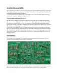
ATV Modulator User Manual
FMTV Modulator by
Grant ZL1WTT & Keith ZL1BQE
© 20 February 2004
Page 1
Display board layout
The controller consists of a 2x 16 LCD display with three push buttons and a rotary encoder.
The push button on the rotary encoder changes the stepping size.
Button A is the menu select. Button B selects between VFO and Memories 0 to 99.
Button C selects between VFO and the preloaded presets. Turning the rotary encoder
clockwise increase the selected value, anticlockwise will decrease the value.
VFO B or C
Memory B
Preset memory C
Button A: menu functions
Step 1: Entering local oscillator offsets. For the 23cm band, the offset value is 0 so the IF
frequency is displayed. Other bands above 1.2 GHz can have a positive or negative offset
value entered. This will allow the correct RF frequency to be displayed. In this mode, button B
is the 1 GHz step size. The pushbutton on the rotary encoder selects the 100 MHz step.
Button C is used to select between positive or negative offsets.
Step 2: Adjusting the transmit frequency. Pressing the rotary encoder pushbutton changes
the steps sizes from between 50 KHz to 5 MHz.
Step 3: Adjusting the Modulation settings for either positive or negative. This is designed for
use with a high side local oscillator in an up-converter.
Step 4: Deviation setup: The PWM voltage range is 0 to 4.99 volts but only 1 volt of this
range is used. The number displayed on the right sets the start point. The deviation will be
shown as a percentage on the left.
Page 2
Step 5: Video input switching. Position A is for an external input. Position B is intended for
use with an internal pattern and call sign generator, or an alternative video signal source.
Step 6: Sound sub-carrier A / Sound channel 1 on / off switch. This menu entry allows the
sound carrier to be turned on or off.
Step 7: Sound sub-carrier A / Sound channel 1 frequency. The sound sub-carrier frequency
can be adjusted from 5.468 to 7.805 MHz in 7.8125 KHz steps. Pushing the button on the
rotary encoder increases the step size by a factor of 10, i.e. 781.25 KHz.
Step 8: Sound sub-carrier B / Sound channel 2 on / off switch. This menu entry allows the
sound carrier to be turned on or off.
Step 9: Sound sub-carrier B / Sound channel 2 frequency. The sound sub-carrier frequency
can be adjusted from 5.468 to 7.805 MHz in 7.8125 KHz steps. Pushing the button on the
rotary encoder increases the step size by a factor of 10, i.e. 781.25 KHz.
Step 10: RF Power Adjust. Selecting this allows you to change between high and low output
power, by changing the LM2941 regulator’s output voltage..
Step 11: RF Power Control. This turns the output RF on or off via the LM2941 regulator
output.
Step 12 Auxiliary switch 1 on / off or on if modulator PLL is out of lock.
Step 13 Auxiliary switch 2 on / off.
Step 14 ASCII identification you can enter up to 16 charcters to fit on the top line of the
display. This function will only be useable in programmable memory mode.
At this point you exit back to the mode that you started from
Page 3
ATV Modulator Setup Information
LM2941 Regulator set up
Power settings to control a power block output stage for M67715 or M68719. There are two
preset pots on PCB next to LM2941 regulator. One set up the low voltage and the other sets
the high voltage levels. This regulator can also be turned off via its on / off pin.
The DC voltage is feed via the F-connector across to the bias pin or pin 3 of the power block.
With RF chokes on each of the PCBs, the RF and DC are feed along the coaxial cable that is
used between these two modules.
DC feed voltage can also be set up to power an up converter.
Modulator output level
Between 10mW to 100mW out of ERA-5 drive stage.
VCO lock range
0 to 14 volts 1175 MHz to 1325 MHz depending on VCO set up.
Modulator bandwidth
0 to 30 MHz adjustable with 1 volt peak to peak into 75 ohms video input.
Video bandwidth
For PAL TV system DC to 5.2 MHz
Sound sub-carrier frequency range
From 5.468 to 7.805 MHz in 7.8125 KHz steps.
Sound PLL divider range frequency / 999 to 700.
Sound modulation bandwidth
20 Hz to 100 KHz x2.
Auxiliary switches
Are designed for extra switching if need.
Auxiliary switch 1 can use with an LED and resistor for out of lock indicator.
Communication bus
Can be mounted with a RS232 interface.
DC volts
Input voltage into modulator 13.8 volts at 400 mA. With out the patten generator and the
power block connected to this 13.8 volts supply.
MC68HC908s and the 24LC64 are preprogrammed devices
All PCBs are mounted in a 1U 19“ rack case L 424 x H 38 x W 254mm
See next page for layout information.
Page 4
Modulator 1U 19“ rack case layout
Page 5
Component parts lists & circuit digrames
Display board
Resistors
Capacitors
I.C.s
22k x 1
4.7k x 13
1k x 1
220 x 1
47uF x 1
2.2uF x 1
0.1uF x 3
1nF x 2
2x16 LCD x 1
10MHz osc x 1
MC68HC908QY4 x 1
24LC64 x 1
78L05 x 1
Other bits
Rotary encoder x 1
push buttons x 3
Red LED x 1
Green LED x 1
PCB size 38mm x 174mm
Page 6
Sound board
Resistors
Capacitors
Transistors
Trimpots
RF Chokes
100k x 2
68k x 2
56k x 2
47k x 4
33k x 2
22k x 2
10k x 6
4.7k x 2
2.2k x 6
1k x 4
220 x 3
100 x 2
39 x 2
47uF x 1
33uF x 2
10uF x 2
2.2uF x 1
1uF x 2
0.1uF x 12
0.01uF x 4
3.3nF x 2
1nF x 4
270pF x 4
56pF x 2
10pF x 2
8.2pF x 2
MPF102 x 2
BC549 x 2
100k x 2
10k x 2
2k x 2
560uH x 2
100uH x 2
10uH x 2
Diodes
BB212 x 2
1N914 x 2
I.C.s
Diecast box
From RS 120 x 100 x 35
Stock number 225-209
78L05 x 1
MC68HC908QT1 x 1
MC145149 x 1
LM358 x 1
PCB size 86mm x 101mm
Page 7
Modulator board
Resistors
Capacitors
Transistors
Trimpots
RF Chokes
680k x 1
470k x 1
47k x 1
27k x 1
22k x 1
15k x 1
10k x 1
4.7k x 10
4.7k x 1 SMD*
1k x 2
680 x 4
470 x 1
470 x 1 SMD*
300 x 1
220 x 3
150 x 1
120 x 2 SMD*
82 x 2
75 x 2
47 x 1 SMD*
39 x 1
18 x 1
6.8 x 1
220uF x 1
100uF x 1
22uF x 1
10uF x 5
4.7uF x 2
2.2uF x 1
1uF x 4
0.1uF x 10
1nF x 2
680pF x 1
100pF x 1
47pF x 3 SMD*
10pF x 1 SMD*
MPF102 x 1
BC548 x 5
BFR91 x 2
2k x 3
10uH x 1
Others x 6
Relays
Diodes
Mini 12V x 2
1N4004 x 1
1N914 x 3
BB149A x 3 SMD*
LED red x 1
I.C.s
7809 x 1
78L09 x 1
78L05 x 1
LM2941 x 1
NE592N8 x 1
ERA-5 x 1
MC68HC908QT1 x 1
MC68HC908QY4 x 1
MB1501 x 1
PCB size 70mm x 212mm
Page 8
Interface board
Resistors
Capacitors
Transistors
10k x 2
4.7k x 3
3.9k x 1
1uF x 1
BC548 x 2
BC558 x 1
Diodes
5V1 x 1
1N4148 x 2
PCB size 40mm x 23mm
Page 9