1
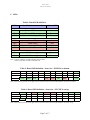
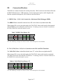
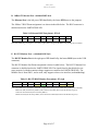
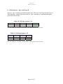
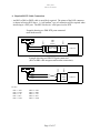
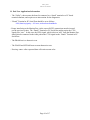
RPXL_UM.fm
RPX Lite User’s Manual
Embedded Planet, LLC (16Jun00)
RPX Lite User’s Manual - for Rev CW boards
User’s Manual for the RPXL
WEB site @ www.embeddedplanet.com
Revision Control:
09JUN99
16JUN00
First Release.
Minor corrections identified by change bars
Table of Contents
I.
Overview . . . . . . . . . . . . . . . . . . . . . . . . . . . . . . . . . . . . . . . . . . 3
A.
B.
II.
Jumpers, Switches, and LEDs . . . . . . . . . . . . . . . . . . . . . . . . . . 6
A.
B.
C.
III.
Jumpers JP1 and JP4. . . . . . . . . . . . . . . . . . . . . . . . . . . . . . . . . . . . 6
Dip Switch . . . . . . . . . . . . . . . . . . . . . . . . . . . . . . . . . . . . . . . . . . . 6
LEDs . . . . . . . . . . . . . . . . . . . . . . . . . . . . . . . . . . . . . . . . . . . . . . . . 7
Connectors/Headers . . . . . . . . . . . . . . . . . . . . . . . . . . . . . . . . . . 8
A.
B.
C.
D.
E.
F.
G.
H.
IV.
Top View of Board . . . . . . . . . . . . . . . . . . . . . . . . . . . . . . . . . . . . . 4
Bottom View of Board . . . . . . . . . . . . . . . . . . . . . . . . . . . . . . . . . . 5
DEBUG Port - 2x5 (0.1 x 0.1) header . . . . . . . . . . . . . . . . . . . . . . 8
TAP (JTAG) Port - 2x5 (0.1 x 0.1) header . . . . . . . . . . . . . . . . . . . 8
UTILITY Header - 2x8 (0.1 x 0.1) header . . . . . . . . . . . . . . . . . . . 9
10Base-T Ethernet Port - shielded RJ45 Jack. . . . . . . . . . . . . . . . 10
RS-232 Monitor Port - a shielded RJ45 Jack . . . . . . . . . . . . . . . . 10
USB Connector - Type A and Type B . . . . . . . . . . . . . . . . . . . . . 11
Power Connector (Barrel Type) and Specifications . . . . . . . . . . . 12
Processor Bus and I/O Interface/Expansion Receptacles - 2x60 . 13
RPXL Utility Software. . . . . . . . . . . . . . . . . . . . . . . . . . . . . . . 14
A.
B.
C.
Required RS232 Cable Connections. . . . . . . . . . . . . . . . . . . . . . . 15
End User Applications Information . . . . . . . . . . . . . . . . . . . . . . . 16
Typical Monitor Listing . . . . . . . . . . . . . . . . . . . . . . . . . . . . . . . . 17
Page 1 of 17
RPXL_UM.fm
RPX Lite User’s Manual
List of Tables
HW Features . . . . . . . . . . . . . . . . . . . . . . . . . . . . . . . . . . . . . . . . . . . . . . . . . . . . . 3
Jumper Settings . . . . . . . . . . . . . . . . . . . . . . . . . . . . . . . . . . . . . . . . . . . . . . . . . . . 6
Dip Switch Settings . . . . . . . . . . . . . . . . . . . . . . . . . . . . . . . . . . . . . . . . . . . . . . . . 6
Board LED definition . . . . . . . . . . . . . . . . . . . . . . . . . . . . . . . . . . . . . . . . . . . . . . 7
Board LED definition - front view - PCMCIA on bottom . . . . . . . . . . . . . . . . . . 7
Board LED definition - front view - if PCMCIA on top . . . . . . . . . . . . . . . . . . . . 7
DEBUG Port Pinout - P6 . . . . . . . . . . . . . . . . . . . . . . . . . . . . . . . . . . . . . . . . . . . . 8
TAP (JTAG) Port Pinout - P7 . . . . . . . . . . . . . . . . . . . . . . . . . . . . . . . . . . . . . . . . 8
Utility Header Pinout - P14 . . . . . . . . . . . . . . . . . . . . . . . . . . . . . . . . . . . . . . . . . . 9
Ethernet RJ45 Port pinout - P3 left . . . . . . . . . . . . . . . . . . . . . . . . . . . . . . . . . . . 10
RS-232 RJ45 Monitor Port pinout - P3 right . . . . . . . . . . . . . . . . . . . . . . . . . . . . 10
USB Type A pinout - P4 . . . . . . . . . . . . . . . . . . . . . . . . . . . . . . . . . . . . . . . . . . . 11
USB Type B pinout - P5 . . . . . . . . . . . . . . . . . . . . . . . . . . . . . . . . . . . . . . . . . . . 11
Page 2 of 17
RPXL_UM.fm
RPX Lite User’s Manual
I.
Overview
The RPX Lite is a highly integrated SBC based on the Motorola MPC850 and MPC823. The
MPC850 versions are targeted for the tel-com industries, while the MPC823 version is targeted
for the industrial controls market.
Support is available for several commonly used RTOSs.
The RPX Lite is in a PC104 board form factor. It does not contain PC104 (ISA) or PC104+ (PCI)
functionality, but rather adheres to the mechanical specifications of the PC104 standard. For
PC104 (ISA) and/or PC104+ (PCI) requirements, see the RPX Classic User’s Manual.
The functions included on the RPX Lite are listed as follows:
Table 1: HW Features
Entity
Function
Processor
DRAM
FLASH
NVRAM
10Base-T Ethernet
Monitor Port
Serial EEPROM
Serial Temp & Thermal Monitor
Debug
TAP
PCMCIA
USB
Dip Switch
LEDs
MPC850 (SR, DC, DH, etc.) or MPC823
4MB or 16MB
2MB, 4MB, 8MB, or 16MB
0KB, 32KB, 128KB, 512KB
SCC2 - 10Base-T (RJ45)
SMC1 -3 wire RS232 (RJ45)
I2C
I2C
Development Port header for BMD
TAP header for Test and JTAG
Single Slot - Type I, II, or III
Type A or Type B Connector
4 position slide switch read via status register
Two user programmable via control register
Processor Bus Interface Expansion Receptacle
Bus Expansion Receptacle1
I/O Expansion Receptacle1
Wall-Cube Power Supply
BCSR’s
Processor I/O Interface Expansion Receptacle
Single Power Supply Source for Board
(Board draws 1A max)
BCSR0, 1, 2, and 3
The Expansion Receptacles allow for daughter cards supporting such functions as CAN,
ARCNET, T1/E1, xDSL, PCI via PC104+, etc.
Note: External KAPWR, via battery on P14.15-16, not supported on the RPXL
or LITE series of CPU cards. For battery backup of a RTC, use the
LITE_DW.
Page 3 of 17
RPXL_UM.fm
RPX Lite User’s Manual
For Programming Information, see the RPX Lite Programmer’s/Firmware Manual
All spacial orientations referenced in this document assume the board is oriented with the
RJ45 connector on top, with the entry to the RJ45 connector considered the front of the
board.
A. Top View of Board
5V
Page 4 of 17
RPXL_UM.fm
RPX Lite User’s Manual
B. Bottom View of Board
3V
HRST
BB
LED5
LED4
Page 5 of 17
LIG
RXD
TXD
RPXL_UM.fm
RPX Lite User’s Manual
II.
Jumpers, Switches, and LEDs
A. Jumpers JP1 and JP4
Table 2: Jumper Settings
Function of JP1
JP1
JP4
Function of JP4
External 3.0V Battery Connected
E
D
Processor pins have DEBUG signals selected
No External Battery Connected
O
T
Processor pins have IEEE1149 signals selected
Note: Jumpers as shown in table when looking down on the Jumpers.
JP4 must have a jumper inserted.
JP1 does not require a jumper. No jumper is the same as setting “O” (no external battery connected).
B. Dip Switch
There is a 4-pole dip-switch located on the board. These switches are readable via the on-board
status register. The switch is intended for use by specific customer applications.
The switch in the down = on = closed position will read back a logic ‘0’ in the status register.
The switch in the up = off = open position will read back a logic ‘1’ in the status register.
Table 3: Dip Switch Settings
Encoded Pole
Positions
4321
D(27:24)
0000 or 1111
0001
0010
0011 through 1110
Function
Normal operating mode
Reserved for manufacture test
Reserved for fall-back mode
User specified
Page 6 of 17
RPXL_UM.fm
RPX Lite User’s Manual
C. LEDs
Table 4: Board LED definition
LED #
Led Definition when “on”
Color of LED
CR9
CR10
CR12
Ethernet TXD activity
Ethernet RXD activity
Ethernet Link Integrity Good
Green
Green
Green
CR2
CR3
CR6
CR8
Status LED4
Status LED5
Processor Activity (BB# signal)
Processor Hard Reset Active
Red
Red
Green
Red
CR1
CR14
+3.3V Power Applied
+5.0V Power Applied
Green
Green
Note: Color of “shading” in Table indicates color of LED.
CR14 on top side, all others on bottom side.
Table 5: Board LED definition - front view - PCMCIA on bottom
Function
LED
LED
Function
CR9
ETXD
CR10
ERXD
CR12
ELIG
CR2
LED4
CR3
LED5
CR6
BB
+5.0V
CR14
CR1
+3.3V
CR8
HRST
Note: LED ordering is from left to right when viewed from front of board with PCMCIA connector on bottom.
Table 6: Board LED definition - front view - if PCMCIA on top
Function
LED
LED
Function
+3.3V
CR1
CR14
+5.0V
HRST
CR8
BB
CR6
LED5
CR3
LED4
CR2
ELIG
CR12
ERXD
CR10
Note: LED ordering is from left to right when viewed from front of board with PCMCIA connector on top.
Page 7 of 17
ETXD
CR9
RPXL_UM.fm
RPX Lite User’s Manual
III.
Connectors/Headers
The RPX Lite contains 3 headers for auxiliary functions, 2 RJ45 connectors for Ethernet Port and
the RS232 Monitor Port, 1 USB connector, 1 barrel connector for power, and 2 daughter card
interface/expansion Receptacles, all of which are described below.
A. DEBUG Port - 2x5 (0.1 x 0.1) header for a Backround Mode Debugger (BMD)
The DEBUG Port is identified with the letter “D” on the silkscreen (middle header P6).
When jumper JP4 is set to select this mode, the TAP (JTAG) chain on the board is disconnected
and the DEBUG port is dedicated to the Processor. No mating connector should be attached to
the TAP (JTAG) Port when this mode is active.
Table 7: DEBUG Port Pinout - P6
Pin Number
Function
Function
Pin Number
9
+3.3V
DSDO
10
7
HRST#
DSDI
8
5
GND
FRZ
6
3
GND
DSCK
4
1
FRZ
SRST#
2
Note: Pin numbering 1 through 10 as shown in table is when looking down onto the header.
B. TAP (JTAG) Port - 2x5 (0.1 x 0.1) header for the TAP and JTAG Functions
The TAP (JTAG) Port is identified with the letter “T” on the silkscreen (right header P7).
When jumper JP4 is set to select this mode, the TAP (JTAG) chain on the board is completed.
The chain is Processor first, then the CPLD device. No mating connector should be attached to
the DEBUG Port when this mode is active.
Table 8: TAP (JTAG) Port Pinout - P7
Pin Number
Function
Function
Pin Number
9
TCK
GND
10
7
TMS
GND
8
5
TDO
+3.3V
6
3
TDI
GND
4
1
TRST#
GND
2
Note: Pin numbering 1 through 10 as shown in table is when looking down onto the header.
Page 8 of 17
RPXL_UM.fm
RPX Lite User’s Manual
C. UTILITY Header - 2x8 (0.1 x 0.1) header for resets, power, and power fail interrupt
The UTILITY HEADER is the left header P14.
The Utility Header is used to allow for external connections.
Three types of reset signals can be connected to the header (Hard Reset, Soft Reset, and/or Power
On Reset).
The PFIRQ0# signal is routed to interrupt level 0 on the processor and could be used as a Power
Fail Interrupt signal.
Three different values of power supply can be connected to the header (+12.0V, V_Plus, and/or
V_Minus). The voltages could be used for daughter card requirements, or in case of the +12.0V,
certain PCMCIA cards. The +12.0V must be +12.0V, but the V_PLUS and V_MINUS could be
any DC voltage (up to 24Vdc) as required by daughter cards. Optionally, a separate header could
be provide by the daughter card for its’ required power supply.
The EXT_BATTERY signal is for connecting an external battery to back up the real-time clock
and keep alive power circuits inside the Processor. The on-board NVRAM has its’ own battery
and is not associated with the EXT_BATTERY signal. The EXT_BATTERY signal does NOT
have any connection to the supplies powering and operating the board.
Table 9: Utility Header Pinout - P14
Pin Number
Function
Function
Pin Number
Notes:
15
EBA
T
GND
16
13
V_MINUS
11
+12.0V
9
V_PLUS
7
PFIRQ0#
5
SRST#
3
POR#
1
HRST#
GND
14
GND
12
GND
10
GND
8
GND
6
GND
4
GND
2
1) Pin numbering 1 through 16 as shown in table is when looking down onto the header.
2) Signals HRST#, POR#, and SRST# must be open drain or open collector type signals.
3) Pins 1, 3, 5, and 7 are input signals (digital +3.3V signals)
4) Pins 9, 11, 13, and 15 are input voltage signals (voltages that can be supplied to these pins)
5) EBAT not supported. Pins reserved for future use.
Page 9 of 17
RPXL_UM.fm
RPX Lite User’s Manual
D. 10Base-T Ethernet Port - shielded RJ45 Jack
The Ethernet Port is the left port of P3 identified by the letters ETH (next to the jumpers).
The 10Base-T RJ45 Pinout assignment is as shown in the table below. The RJ45 connector is
shielded and tied to EARTH GROUND.
Table 10: Ethernet RJ45 Port pinout - P3 left
Pin Number
Function
1
TXD+
2
TXD-
3
RXD+
4
5
6
RXD-
7
8
Note: Pin numbering 1 through 8 is from left to right when looking into the RJ45 Jack (locking tab on bottom).
E. RS-232 Monitor Port - a shielded RJ45 Jack
The RS-232 Monitor Port is the right port of P3 identified by the letters MON (next to the USB
connector).
The RS-232 Monitor Port Pinout assignment is shown in table below. The RS-232 Monitor Port
connector is shielded and tied to EARTH GROUND. The signals listed in the table below are
surge protected, with the transient voltage suppressors connected to EARTH GROUND. The
Monitor Port is from SMC1, and as such, only supports a three wire interface (no handshaking).
Table 11: RS-232 RJ45 Monitor Port pinout - P3 right
Pin Number
Function
1
2
3
DTR#
4
GND
5
RXD
6
TXD
7
CTS#
8
RTS#
Note: Pin numbering 1 through 8 is from left to right when looking into the RJ45 Jack (locking tab on bottom).
RTS# not used (not driven by SMC1) and is tied true on board (driven true all the time on pin 8).
CTS# not used on board (not received by SMC1).
DTR# not used (not driven by SMC1) and is tied true on board (driven true all the time on pin 3).
Page 10 of 17
RPXL_UM.fm
RPX Lite User’s Manual
F. USB Connector - Type A and Type B
Only one “type” connector is installed on the board. The Type A and Type B connectors are
“dual footprints” on the PCB, and as such, the “type” connector is a manufacturing option
specified at time of order.
Table 12: USB Type A pinout - P4
Pin Number
Function
1
+5.0V
2
DATA-
3
DATA+
4
GND
Note: Pin numbering 1 through 4 is from left to right when looking into the Connector.
Table 13: USB Type B pinout - P5
Function
Pin Number
Pin Number
DATADATA+
2
3
1
4
Function
+5.0V
GND
Note: Pin numbering 1 through 4 as shown in table is when looking into the Connector.
Page 11 of 17
RPXL_UM.fm
RPX Lite User’s Manual
G. Power Connector (Barrel Type) and Specifications
The power connector is a barrel type connector. The specifications for the mating connector
are as follows:
Inner diameter = 2.5mm (.100 inches)
Outer diameter = 5.5mm (.218 inches)
Barrel Length >/= 9.5mm (0.375 inches)
Outer shell is GND
Inner shell is +5.0V
Two options exist for powering the RPXL. The first option is that +5.0V can be supplied through
either the Barrel Connector or through the Expansion Receptacles via an Expansion Card. The
second option is that +3.3V can be supplied through either the Barrel Connector or through the
Expansion Receptacles via an Expansion Card. The option selected must be specified at time of
ordering the product because the option selected is assembly dependent.
If the second option is selected, then the following limitations apply:
1) The USB VCC rail on the USB connector can not be power with 5V from the RPXL, since 5V
is not available on the RPXL. Another source must be used to power the 5V line on the connector
side. Aside from the 5V supply issue on the USB connector, USB fucntionality is still supported.
2) 5V PCMCIA cards are not supported, since 5V is not available on the RPXL.
The DC supply must be a regulated plus and minus 5% +5.0V supply for Option 1. Option
2 requires a 3.2 to 3.4V supply.
The RPX Lite itself, fully configured but with no expansion cards or PCMCIA cards, draws
1.0A maximum @ VCC = 4.75V to 5.25V, T = 0oC-70oC.
Page 12 of 17
RPXL_UM.fm
RPX Lite User’s Manual
H. Processor Bus and I/O Interface/Expansion Receptacles - 2x60 (B8 type)
The Processor Bus Expansion Receptacle is the socket strip on the left side identified by P1.
The Processor I/O Expansion Receptacle is the socket strip on the right side identified by P2.
This interface allows daughters cards to be designed and interfaced to the RPX Lite. All required
signals are routed to the Receptacle to allow for daughter cards that require the Processor
interface. Pins A1 (on left) and B1 (on right) are identified on the PCB.
The connector type chosen allows for variable stacking heights and is an 8mm pitch connector.
This connector is different than those on the Evaluation Units. The change was made to allow for
all the CPM port signals to be available at the receptacle, with additional ground pins added to aid
in signal integrity.
The standard RPXL product board to board mating distance is 16mm. Available stacking heights
range from 4.5mm to 20mm. The receptacle part number used on the standard product is
AMP 5-179010-5. The mating connector (Plug) is AMP 179031-5, which would be used on
Expansion Card designs. As an alternative, Yamaichi Electronics also makes the same type of
connector that “fits” in the same PCB footprint, but the connector is sold in sets (receptacle and
plug sold together). The Yamaichi part number is B8-120-665-1Ax1-N.
For signal loading considerations, refer to the Expansion Card Design Guidelines document.
The Processor Bus Expansion Receptacle (P1) or interface must be a 3.3V only type of
interface (the I/O is not 5.0V I/O tolerant).
The Processor I/O Expansion Receptacle (part of P2) or interface is currently +5.0V tolerant, but
indications from the Motorola Semiconductor Sector claim that future processors will NOT be
+5.0V tolerant on I/O pins. Therefore, it is highly recommended that I/O interfaces on
daughter cards be designed for true +3.3V operation.
For the pinout of the P1 and P2 receptacles, see the pinouts document.
Page 13 of 17
RPXL_UM.fm
RPX Lite User’s Manual
IV.
RPXL Utility Software
The RPXL, in its’ simplest form, is shipped with Embedded Planet boot-up and diagnostic software,
here in called “Start-Up” code. This “Start-Up” code verifies the integrity of the hardware, allows
configuration changes, and allows downloading of user code. Additional functionality will be
added to this code, and as the additional functionality becomes available, the program will be
updated, and made available. Upgrades are provided as files containing Motorola
S-records. The S-record data is a program which is downloaded to DRAM either using the
monitor serial port and a terminal emulation program, or using the ethernet port and a tftp server.
Once downloaded one runs the program which then replaces the regions of FLASH containing the
RPX Utility Software.
Page 14 of 17
RPXL_UM.fm
RPX Lite User’s Manual
A. Required RS232 Cable Connections
- An RJ45 to DB9 or DB25 cable is most likely required. The pinout of the RJ45 connector
is shown in Section III.E above. A “null modem” type of connection will be required when
interfacing to a DTE port. The RPX Lite has its’ serial port wired as DTE.
Example showing two DB9 DTE ports connected
(null modem used):
TXD
RXD
GND
(DB9)
DB9
Null
Modem
(DB9)
1 2 3 4 5 6 7 8
3
3
3
3 - TXD
2
2
2
2 - RXD
5
5
5
5 - GND
DTE Port
(DB9)
1 2 3 4 5 6 7 8
TXD
RXD
GND
For DTE:
DB9-3 = TXD
DB9-2 = RXD
DB9-8 = CTS
DB9-7 = RTS
DB9-5 = GND
DB25-2 = TXD
DB25-3 = RXD
DB25-5 = CTS
DB25-4 = RTS
DB25-7 = GND
Page 15 of 17
(DB9)
Example showing two DB9 DTE ports connected
(RJ45 to DB9 cable integrates null modem connection):
3
3 - TXD
2
2 - RXD
5
5 - GND
DTE Port
RPXL_UM.fm
RPX Lite User’s Manual
B. End User Applications Information
- The “Utility” code assumes the board is connected to a “dumb” terminal or a PC based
terminal emulator, and requires user intervention for the diagnostics.
- “Dumb” Terminal or PC Serial Port should be set as follows:
9600, data/stop/parity = 8/1/none, no hardware handshake
- Proper interfacing to the Monitor Port via the correct RS232 connections must be insured
per the previous section. The “Dumb” Terminal or PC Serial Port might require the CTS#
signal to be “true”. In this case, the RTS# signal, which is driven “true” from the Monitor Port,
should also be connected in the cable path to the CTS# signal on the “Dumb” Terminal or PC
Serial Port.
- The DRAM test is a destructive test.
- The FLASH and NVRAM tests are non-destructive tests.
- Pressing <enter> after requested data will retain current value.
Page 16 of 17
RPXL_UM.fm
RPX Lite User’s Manual
C. Typical Monitor Listing
DRAM1:wwwwwvvvvvCCCCCVVVVV NVRAM:VVVVVV
----------------------------------------------------------------------------------------RPX utility program, Copyright 1998, RPCG LLC, All Rights Reserved.
Reset(0100): ExHard ExSoft, TESR:0000
BCSR : OK
RTC
: OK, battery LOW or absent, tics/sec=1, time = 2 sec
I2C
: OK, STTM : OK 23.5c, EEcfg: OK, 128 bytes, checksum: 18CE
ENET : OK, 00:10:EC:00:00:16
FLASH : OK, 4 Mb, id=01:49, cs:A939 es:A939 OK (FFF00000 FFF20000)
NVRAM: OK, 32Kb, NVR battery GOOD
DRAM : OK, 16Mb, 10 columns
RPX-Lite 823 50Mhz CoreCp=2100:0000 Ic, ~Dc, RPXU v1.21
===> RPX Utility Main Menu:
1 test BCSR
T display Time & Temperature
2 test dip switches
3 test LEDs
C Configure EEPROM
4 test I2C, STTM, EEPROM, CFG L Load RAM
5 test FLASH
P Program FLASH
6 test NVRAM/SRAM
S Scan FLASH for executables
7 test DRAM (destructive)
B rpxBug command line
8 test Ethernet
9 run all tests
R hard Reset
===> RPX Utility Main Menu: Press 123456789 T CLPSB or R key : <?> : *
Page 17 of 17