1
ADMCF327
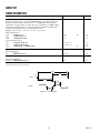
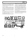
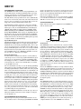
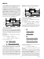
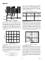
2. Program PWMSYNCWT to proper count as in Figure 13.
The auxiliary PWM system of the ADMCF327 can operate in
two different modes: independent mode or offset mode. The
operating mode of the auxiliary PWM system is controlled
by Bit 8 of the MODECTRL register. Setting Bit 8 of the
MODECTRL register places the auxiliary PWM system in the
independent mode. In this mode, the two auxiliary PWM generators are completely independent and separate switching
frequencies and duty cycles may be programmed for each auxiliary PWM output. In this mode, the 8-bit AUXTM0 register
sets the switching frequency of the signal at the AUX0 output
pin. Similarly, the 8-bit AUXTM1 register sets the switching
frequency of the signal at the AUX1 pin. The fundamental time
increment for the auxiliary PWM outputs is twice the DSP
instruction rate (or 2 tCK) and the corresponding switching
periods are given by:
3. The ADC Max Count is calculated, as described in a previous section.
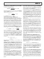
TAUX1 = 2 × (AUXTM1 + 1) × tCK
ADC Reference Ramp Calibration
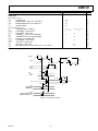
The peak of the ADC ramp voltage should be as close as possible
to 3.5 V to achieve the optimum ADC resolution and signal range.
When the current source is in the Default State, the peak of the
ADC ramp slope will be lower than this “3.5 V” target ramp.
When the current source value is increased, the ADC ramp
slope will become closer to the target value. The “tuned” ramp
slope is the one closest to the target ramp.
A simple calibration procedure using the internal 2.5 V reference
voltage allows the selection of the ICONST_TRIM register
value to reach this:
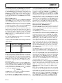
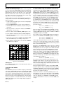
1. A high quality linear ADC capacitor is selected using Figure
14 for a tuned ICONST.
TAUX0 = 2 × (AUXTM0 + 1) × tCK
4. The target reference conversion is calculated as TARGET =
(Max Count) × (2.5 V/3.5 V).
Since the values in both AUXTM0 and AUXTM1 can range
from 0 to 0xFF, the achievable switching frequency of the
auxiliary PWM signals may range from 39.1 kHz to 10 MHz for
a CLKOUT frequency of 20 MHz.
5. Reset or software sets the ICONST_TRIM register to zero.
6. Select calibration channel in software on ADC multiplexer.
The on-time of the two auxiliary PWM signals is programmed
by the two 8-bit AUXCH0 and AUXCH1 registers, according to:
7. The calibration channel value is compared with the target
reference conversion.
TON, AUX0 = 2 × (AUXCH0) × tCK
8. If this value is greater than the TARGET, the ICONST_TRIM
value is incremented by one, and Step 7 is repeated.
TON, AUX1 = 2 × (AUXCH1) × tCK
so that output duty cycles from 0% to 100% are possible. Duty
cycles of 100% are produced if the on-time value exceeds the
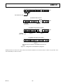
period value. Typical auxiliary PWM waveforms in independent
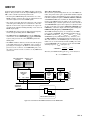
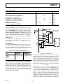
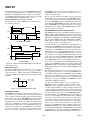
mode are shown in Figure 16(a).
9. If the calibration channel value is less than the TARGET,
the calibration is completed.
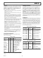
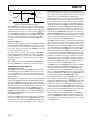
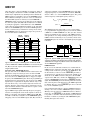
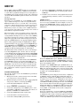
3.5V
When Bit 8 of the MODECTRL register is cleared, the auxiliary
PWM channels are placed in offset mode. In offset mode, the
switching frequency of the two signals on the AUX0 and AUX1
pins are identical and controlled by AUXTM0 in a manner
similar to that previously described for independent mode. In
addition, the on times of both the AUX0 and AUX1 signals are
controlled by the AUXCH0 and AUXCH1 registers as before.
However, in this mode the AUXTM1 register defines the offset
time from the rising edge of the signal on the AUX0 pin to that
on the AUX1 pin according to:
TARGET
RAMP
VREF
MINIMUM
RAMP
TOFFSET = 2 × (AUXTM1 + 1) × tCK
0.3V
Figure 15. Current Ramp
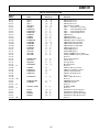
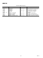
ADC Registers
The configuration of all registers of the ADC System is shown at
the end of the data sheet.
AUXILIARY PWM TIMERS
Overview
The ADMCF327 provides two variable frequency, variable duty
cycle, 8-bit, auxiliary PWM outputs that are available at the AUX1
and AUX0 pins when enabled. These auxiliary PWM outputs
can be used to provide switching signals to other circuits in a
typical motor control system such as power factor corrected
front-end converters or other switching power converters. Alternatively, by addition of a suitable filter network, the auxiliary
PWM output signals can be used as simple single-bit digital-toanalog converters.
REV. 0
For correct operation in this mode, the value written to the
AUXTM1 register must be less than the value written to the
AUXTM0 register. Typical auxiliary PWM waveforms in offset
mode are shown in Figure 16(b). Again, duty cycles from 0% to
100% are possible in this mode.
In both operating modes, the resolution of the auxiliary PWM
system is eight bits only at the minimum switching frequency
(AUXTM0 = AUXTM1 = 255 in independent mode, AUXTM0
= 255 in offset mode). Obviously, as the switching frequency is
increased, the resolution is reduced.
Values can be written to the auxiliary PWM registers at any
time. However, new duty cycle values written to the AUXCH0
and AUXCH1 registers only become effective at the start of the
next cycle. Writing to the AUXTM0 or AUXTM1 registers
causes the internal timers to be reset to 0 and new PWM cycles
to begin.
–19–