1
a
ONE TECHNOLOGY WAY
AN-407
APPLICATION NOTE
• P.O.
BOX 9106
• NORWOOD,
MASSACHUSETTS 02062-9106
• 617/329-4700
AC Motor Control Experiments
Using the ADMC200-EVAL Board
by Aengus Murray and Paul Kettle
INTRODUCTION
The ADMC200-EVAL board can be used to build a simple
motor control demonstration based around the ADMC200
motion coprocessor. The board is designed to interface
directly to the ADDS-2101-EZ-LAB or the ADMC21xxEZ-LAB boards through the 60-pin user interface connector. This board can be used with processors that are
compatible with the ADMC200 address and data bus.
The evaluation board is supplied with a DSP assembly
code for a demonstration program that exercises all the
ADMC200 functions.
A more detailed description of the ADMC200 functions and pinout is included in the product data
sheet. There is also a companion application note
describing the digital implementation of a high
speed motor control systems using the ADMC200/
ADMC201 and an ADSP-2105 DSP.
This document only relates to REV 2.0 of the
ADMC200-EVAL board and REV 2.0 of the demonstration software.
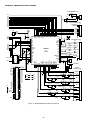
ADMC200-EVAL BOARD HARDWARE
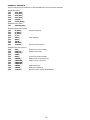
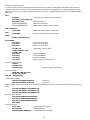
The system block diagram is shown in Figure 1,
while the full circuit diagram is in Appendix A. The
board has the ADMC200/ADMC201 as the main component, a 74S138 address decoder, a 74LS04 hex inverting buffer, and some passive components. The
user connections to the board are made via three terminal blocks: PWM output, analog input, and digital
I/O. Separate analog (5 VA) and logic (5 VL) power is
supplied through a 4-way terminal block.
The software provided with the evaluation board serves
two purposes. Running the software demonstrates
ADMC200 functions and verifies the operation of the IC.
The software can also serve as a useful template around
which to write motor control software using the
ADMC200.
This application note describes the ADMC200-EVAL
board hardware, setting up with the ADSP-2101 EZ-LAB
board, and a description of the demonstration software.
Instructions on how to load and run the software is given
in the Running the Demonstration Program section.
The analog input channels have Zener diode protection and a two-pole passive anti-aliasing filter with a
default cutoff frequency of 5 kHz. The reference input
D0..11 A0..3
WR RD CLK
ADMC200
J
P
1
7
4
0
4
PWMSTOP
RESET
CS
U V W AUX
POWER CONNECTOR
A
AP
B
BP
C
CP
PWM CONNECTOR
DIGITAL CONNECTOR
DSP INTERFACE CONNECTOR (FOR ADSP-21xxEZ-LAB
JP2
JPG1..3
RC FILTER
NETWORK
7
4
1
3
8
ADDRESS
DECODE
AD 9..10,
AD 12..13
DMS
ANALOG INPUT CONNECTOR
Figure 1. ADMC200-EVAL Board System Block Diagram
can be taken from the ADMC200/ADMC201 reference
output or through the analog connection block. The
CONVST pin can be connected to the PWMSYNC pin or
to the external digital I/O connector. The ADMC200/
ADMC201 PWM outputs are buffered using a 74LS04 hex
inverter to give active high PWM signals at the connector. Other signal formats can be obtained by using a different buffer.
The ADMC200/ADMC201 A/D converter connections can
be configured using jumpers JP1 and JP2 as described in
Table II. Here, the names in bold are ADMC200/ADMC201
pins, while the names in italic are brought from one of the
terminal blocks. The start of conversion signal can be synchronized to the PWM switching frequency (using
PWMSYNC), or to an external CONVST signal. The A/D
reference (REFIN) can be derived from the on board reference (REFOUT) or through the analog connector.
The ADMC200 board connects to the ADSP-2101 data
and address busses via the 60-pin user interface connector. The ADMC200/ADMC201 data bus is connected to
the top 12 bits of the DSP data bus (D12 . . . D23). The
ADMC200/ADMC201 4-bit address bus is connected to
the lower 4 bits of the DSP address bus (AD0 . . . AD3).
The ADMC200/ADMC201 chip select line CS, is derived
using the 74S138 address decoder from the DSP address
lines AD4, AD5, AD12 and AD13. The memory space
between 1000 and 2FFF is used by the EZ-LAB Digital to
Analog Converter. The ADMC200 read registers are
memory mapped to the DSP data memory between 3000
and 300F. To allow read and write registers to have different names the write registers are mapped between
3010 and 301F. The DSP read, write and output clock
lines are connected directly to the ADMC200. The
ADMC200 interrupt line IRQ is connected to DSP interrupt IRQ2.
Table II. ADMC200/ADMC201-EVAL ADC Jumpers
Jumper Position Function
JP1
JP2
JP3
1–2
Connects PWMSYNC to CONVST
2–3
Connects EXTSAMPLE to CONVST
1–2
Connects REFOUT to REFIN
2–3
Connects REFIN to REFIN
1–2
Connect IRQ on ADMC200/ADMC201
to DSP IRQ2
2–3
Connect IRQ on ADMC200/ADMC201
to DSP IRQ1
Analog Input Signals
Analog inputs to the Analog to Digital (A/D) converter
are brought through a 14-way connector block, described in Table III. There is a two-stage passive antialiasing low-pass filter at the input to each of the A/D
converter channels. The filter R and C values are 10 kΩ
and 3.3 nF which gives a cutoff frequency of 5 kHz. Other
cutoff frequencies can be selected by replacing the resistor networks (7XR DIL isolated resistor network).
Power Supply Connections
The board requires a +5 V power supply. Separate analog (+5 VA and 0 VA) and logic (+5 VL and 0 VL) supply
connections are provided to minimize noise on supply
cables. It is recommended that the logic, analog, and signal grounds be connected to a common star point on the
board using jumpers JPG1. . . .
Table III. ADMC200-EVAL Analog Connector
Jumper Configuration
The board has three ground planes: a logic ground plane
(0 VL), an analog ground plane (0 VA) and a signal
ground plane. These can all be connected to a common
star point using jumpers JPG1 . . . 3 as described in the
following table.
Table I. ADMC200-EVAL Ground Jumpers
Connector
Name
ADMC200 Connection
SHIELD
Connected to 0 VL Ground Plane
SGND
Connected to SGND Ground Plane
U
Connected to U via RC Filter
SGND
Connected to SGND Ground Plane
V
Connected to V via RC Filter
SGND
Connected to SGND Ground Plane
JUMPER
Position
Function
JPG1
IN
Connects Analog Ground 0 VA to
Star Point
W
Connected to W via RC Filter
JPG2
IN
Connects Logic Ground 0 VL to
Star Point
SGND
Connected to SGND Ground Plane
AUX0
Connect to AUX
JPG3
IN
Connects Signal Ground SGND to
Star Point
AUX1
ADMC201 Only
AUX2
ADMC201 Only
AUX3
ADMC201 Only
SGND
Connected to SGND Ground Plane
REFIN
Connected to REFIN (Pin)
–2–
PWM Output Signals
The six PWM outputs signals are buffered by a 74LS04
HEX buffer IC and brought to the 8-way terminal block. If
active low signals are required, direct from the
ADMC200, this inverter IC can be bypassed. The buffer
can be replaced by an open collector device to drive
opto-isolating LED input type gate drive circuits. The
PWM STOP input is brought directly from the connector
to ADMC200. If this input is unused, it should be pulled
low through a 10K resistor to prevent spurious tripping
of the PWM signals.
Data and Address Bus Interface
The ADMC200 board connects to the ADSP-2101 data
and address busses via the 60-pin user interface connector. The ADMC200 4-bit address bus is connected to
the lower 4 bits of the DSP address bus (AD0 . . . AD3).
The ADMC200 chip select line (CS) is derived using the
74S138 address decoder from the DSP address lines
AD9, AD10, AD12 and AD13, according to Table VI. The
memory space between 1000 and 2FFF is used by the
EZ-LAB DAC. The ADMC200 read registers are memory
mapped to the DSP data memory between 0x3000 and
0x300F. To allow read and write registers to have different names the write registers are mapped between
0x3010 and 0x301F. The memory map for the system is
given in Table VII.
Table IV. ADMC200-EVAL PWM Connector
Connector Name ADMC200 Connection
0 VL
Connected to 0 VL Ground Plane
PWMSTOP
Input to ADMC200 STOP Pin
CP
Driven by ADMC200 CP through Buffer
C
Driven by ADMC200 C through Buffer
BP
Driven by ADMC200 BP through Buffer
B
Driven by ADMC200 B through Buffer
AP
Driven by ADMC200 AP through Buffer
A
Driven by ADMC200 A through Buffer
The DSP reads and writes data directly to and from the
ADMC200 registers. The ADMC200 data bus is connected to the top 12 bits of the DSP data bus (D12 . . .
D23), thus lowest 4 bits read by the DSP will always be
invalid. This data bus connection scheme easily allows
the use of the DSP fixed 1.15 mode of operation. Therefore, a full-scale negative input on the A/D converter,
giving 2s complement number 0x800 will be read into
the DSP as 0x8000 HEX or –1.0000000 fixed point (See
Chapter 2 of the ADSP-2100 Family User’s Manual ) . The
ADMC200 interrupt line is connected to DSP interrupt
IRQ2.
Digital I/O Signals
Only two of the digital I/O signals are used with the
ADMC200. An external start of conversion signal can
be supplied via the EXTSAMPLE connection, and the
PWMSYNC pulse is brought out to this connector.
Table V. ADMC200-EVAL Digital I/O Connector
Connector Name
ADMC200 Connection
0 VL
Connected to 0 VL Ground Plane
PIO0
ADMC201 Only
PIO1
ADMC201 Only
PIO2
ADMC201 Only
PIO3
ADMC201 Only
PIO4
ADMC201 Only
PIO5
ADMC201 Only
PWMSYNC
ADMC200 PWMSYNC Output
EXTSAMPLE
External CONVST Signal Input
–3–
Table VI. ADMC200-EVAL Chip Select Logic
21xx EZ-LAB
DMS
AD13
AD12
AD10
AD9
ADMC200-EVAL
DMS
H
A3
X
A2
X
A1
X
A0
X
ADMC200 CS
1
ADMC200 RESET
1
L
1
1
0
0
1
0
L
1
1
0
1
0
1
Table VII. ADMC200-EVAL Memory Map
Address
HEX
Direction
& (Wait States)
0x1000
ADMC200
Address
Mnemonic
Function
W(2)
Write_DAC0_
DAC Channel 0 Data Input
0x1001
W(2)
Write_DAC1
DAC Channel 1 Data Input
0x1002
W(2)
Write_DAC2_
DAC Channel 2 Data Input
0x1003
W(2)
Write_DAC3_
DAC Channel 3 Data Input
0x2000
W(2)
Load_DAC_
Load DAC Data
0x3000
W(0)
ADMC200_RESET_
ADMC200 Chip Reset
0x3000
R(0)
0
ID_PHV1_
Forward/Reverse Rotation Result
0x3001
R(0)
1
IQ_PHV2_
Forward/Reverse Rotation Result
0x3002
R(0)
2
IX_PHV3_
Forward/Reverse Rotation Result
0x3003
R(0)
3
IY_VY_
Forward/Reverse Rotation Result
0x3005
R(0)
5
ADCV_ A/D
Conversion Result
0x3006
R(0)
6
ADCW_ A/D
Conversion Result
0x3007
R(0)
7
ADCAUX_ A/D
Conversion Result
0x3008
R(0)
8
ADCU_ A/D
Conversion Result
0x300E
R(0)
E
SYSSTAT_
System Status Register
0x3010
W(0)
0
RHO_
Forward Rotation Angle Input
0x3011
W(0)
1
PHIP1_VD_
Forward/Reverse Rotation Input
0x3012
W(0)
2
PHIP2_VQ_
Forward/Reverse Rotation Input
0x3013
W(0)
3
PHIP3_
Reverse Rotation Input
0x3014
W(0)
4
RHOP_
Reverse Rotation Angle Input
0x3015
W(0)
5
PWMTM_
PWM Period Input
0x3016
W(0)
6
PWMCHA_
PWM Channel On Time Input
0x3017
W(0)
7
PWMCHB_
PWM Channel On Time Input
0x3018
W(0)
8
PWMCHC_
PWM Channel On Time Input
0x3019
W(0)
9
PWMDT_
PWM Deadtime Input
0x301A
W(0)
A
PWMPD_
PWM Pulse Deletion Input
0x301D
R/W(0)
D
SYSCTRL_
System Control Register
–4–
shown in italic are used to produce CS and RESET signals for the ADMC200. The relevant EZ-LAB DSP connections are shown for reference.
The ADMC200-EVAL board connects to the DSP over
the EZ-LAB user interface connector according to the
following table. Here, the ADMC200 connections in bold
are direct connections to the DSP, while the connections
Table VIII. ADMC200-EVAL DSP Interface Connector
ADSP-2101
ADMC200
Pin
Pin
ADMC200
ADSP-2101
IRQ2
IRQ2
1
2
GND
GND
NC
3
4
NC
NC
5
6
NC
NC
7
8
NC
IRQ1
IRQ1
9
10
NC
HOST_RESET
HOST_RESET
11
12
NC
NC
13
14
NC
NC
15
16
NC
WR
WR
17
18
NC
RD
RD
19
20
GND
GND
GND
21
22
NC
GND
AD0
A0
23
24
NC
AD1
A1
25
26
NC
AD2
A2
27
28
NC
AD3
A3
29
30
D12
D12
GND
GND
31
32
D13
D13
AD4
NC
33
34
D14
D14
AD5
NC
35
36
D15
D15
AD6
NC
37
38
GND
GND
AD7
NC
39
40
D16
D16
AD8
NC
41
42
D17
D17
GND
GND
43
44
D18
D18
AD9
AD9
45
46
D19
D19
AD10
AD10
47
48
D20
D20
AD11
NC
49
50
D21
D21
AD12
AD12
51
52
D22
D22
AD13
AD13
53
54
D23
D23
GND
GND
55
56
GND
GND
DMS
DMS
57
58
CLK
CLOUT
GND
GND
59
60
GND
GND
–5–
Using the ADMC200-EVAL Board with the ADSP-2101
EZ-LAB
To run the supplied demonstration software the ADSP2101 EZ-LAB board IRQ2 must be enabled from the user
interface connector (60-pin IDC), and The FLAG IN pushbutton must be enabled. The required jumper configurations are shown below. If you are using higher clock
frequencies you need to edit the software and run in
the divide-by-two clock mode (see source code listing).
The System Hardware File: ADMC200.SYS (Appendix B)
The system file describes the ADMC200 EVAL and the
ADSP-2101 EZ-LAB board address decode schemes. The
EZ-LAB DAC ports are mapped between memory locations 0x1000 and 0x2000. The ADMC200 reset line
is mapped to the data memory location 0x3000. The
ADMC200 read registers are mapped to data memory
locations running from 0x3000 to 0x300F. The ADMC200
write registers are mapped to data memory locations
running from 0x3010 to 0x301F, this does not effect the
address decode hardware but it allows the use of different register names for data memory reads and writes.
Table IX. ADSP-2101 EZ-LAB Jumper Configuration
Jumper
Position
Function
JP2
3-2
Enable FLAG IN Pushbutton
JP3 . . . JP8
Don’t Care
JP1
2-1
ADMC200 Constants File: ADMC200C.H (Appendix C)
This file includes a number of universal constants used
in the program. The first group of constants define some
ADSP-2101 memory mapped registers. The second
group of constants define ADSP-2101 interrupt masks.
The next group of constants define the bits that must be
set in the ADMC200/ADMC201 system control register to
operate the device in different modes, e.g., AUX_EN:
enable the A/D AUX channel by setting Bit 7. The last set
of constants define the bits in the SYSSTAT register that
should be compared with in order to determine the
ADMC200 interrupt source.
Enable IRQ2 from the User
Interface Connector
ADMC200-EVAL Board Software
The demonstration software exercises the three main
functional blocks on the ADMC200: the A/D converter,
the vector transformation block, and the PWM block.
The program can be loaded on to the EZ-LAB using the
EZ-ICE or by burning a boot EPROM. The program runs
in a loop timed by the ADMC200 A/D converter interrupt
signal that is synchronized to the PWM frequency.
ADMC200 Port File: ADMC200P.H (Appendix D)
This file includes all the port definitions required for the
ADMC200 memory mapped registers.
There are four modes of operation that can be
sequenced through by pressing the FLAG IN button on
the EZ-LAB board:
ADMC200 DSP Code: A200EVAL.DSP (Appendix E)
There is a single file for the main DSP assembly code.
The file can be edited to change the user program
parameters, such as system clock frequency etc., as
listed below. These parameters, in SI units, used to
derive program constants such as the PWM period in
clock counts etc.
• In the ADC_TEST mode the program reads the four
A/D channels and writes the values to the EZ-LAB
DAC outputs DAC0 . . . 3.
• In the FOR_PARK_TEST mode two of the A/D channels V and W are used as the Vd and Vq inputs for a
forward PARK and CLARKE transformation. The rotation angle is incremented at a constant rate and the
PARK results are displayed on DAC0 . . . 2 as a set of
three phase voltages.
The code at the beginning of the program performs
initialization of the DSP and ADMC200. The program is
interrupt driven. The main part of the code consists of
interrupt service routines (ISR) which services the
ADMC200 interrupt. There are two sources of ADMC200
interrupt enabled enabled, namely the A/D conversion
and the Park and Clarke transformation. The ISR is
partitioned into three portions, one for each of the
interrupt sources and an initial portion that parses the
ADMC200 SYSSTAT register to determine the source of
the interrupt and subsequently call one of the two
service portions. The A/D portion of the ISR is subdivided into four sections depending on which one of
four modes is in operation.
• In the REV_PARK_TEST mode the most recent PHV1
. . . 3 results of the forward PARK and CLARKE transformation are used as the PHIP2 and PHIP3 inputs for
a reverse PARK and CLARKE transformation. The rotation angle is again incremented at a constant rate
but this time the PARK results displayed on DAC0 . . .
1 as a set of quadrature sin/cos voltages.
• In the PWM_TEST mode a set of three phase voltages
are incremented by 1 count per PWM cycle, thus
giving a slowly varying duty cycle on each of the
channels.
The source code file can be split into a number of sections:
1.
2.
3.
4.
5.
6.
7.
The demonstration software disks includes a system
file ADMC200.SYS, two include files ADMC200C.H,
ADMC200P.H, the main DSP code A200EVAL.DSP, and a
GO batch file.
–6–
Definition of program constants
Definition of program variables
Interrupt jump table code
Initialization code
Mode change code
Interrupt service routine code
Subroutine code
RUNNING THE ADMC200-EVAL BOARD
DEMONSTRATION SOFTWARE
Running the Demonstration Program
The demonstration software is supplied as source code
and so it must be assembled and linked before being
downloaded onto the EZ-LAB board. The following command line is used to compile the demonstration program.
To run the demonstration you will need dc inputs (between 0 V and 5 V) to at least two of the ADC inputs
PHIP2 and PHIP3. The ADC converts these to a 2s
complement numbers between 8000 (REFIN – 2.5 V) and
7FFF (REFIN + 2.5 V), corresponding to fixed-point
values between –1.0 and +1.0. These ADC inputs are the
Vd and Vq inputs for the FORWARD PARK demonstration, so they must have a vector magnitude less than
1, i.e., Vd2 + Vq2 < 1.
go clock_freq processor_board_rev daughter_board_rev
where clock_freq is either CLK20MHz or CLK12MHz
processor_board_rev is either ADSP2101 or ADMC21xx.
To switch between modes press FLAG key on the
EZ_LAB Board. The demonstration results will be displayed on either the PWM output connector, or the
EZ_LAB DAC connector.
For example the most common configuration would be:
go CLK12MHz ADSP2101
DEMONSTRATION PROGRAM ALGORITHM
For completeness the full demonstration code algorithm is presented in pseudo code format here.
Start:
reset the admc200
setup dsp interrupts
Test1:
read back test
if error flash led
checks sysctrl read/write
start pwm
required to generate convst for ADC
Setup:
Main:
wait for interrupts
if FLAG_IN change mode
IRQ2_ISR:
start of interrupt service routine
check ADMC200 interrupt status
ADC_interrupt:
read U, V, W, AUX
filter V, W and save as vd and vq
select case(mode)
Case(mode=0) (pwm_test)
increment phase voltages
calculate new pwmchx values
write to pwm registers
generates slowly changing pwm
Case(mode=1) (ADC_TEST)
write ADC inputs to DAC
save values as Vd vector
reads ADC and writes to DACs
Case(mode=2) (FOR_PARK_TEST)
increment theta
generates three phase sinewave
write Vd values and theta to park registers
set park read pointer to V_ph
Case(mode=3) (REV_PARK_TEST)
generates quadrature sinewave
increment theta
write V_ph values and theta to park registers
set park read pointer to id
End of ADC interrupt service routine: return to main
Park_interrupt:
read park registers
write values to DAC
save values as V_ph or id vector
End of park interrupt service routine: return to main
–7–
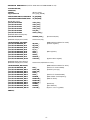
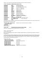
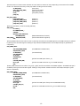
APPENDIX A. ADMC200-EVAL CIRCUIT DIAGRAM
POWER TERMINAL BLOCK
+5VL
C22
10µ
D12
D13
D14
D15
D16
D17
D18
D19
D20
D21
D22
D23
J2
C21
0.1µ
+5VL
1
2
3
4
0VL
CON4
C23
10µ
C24
0.1µ
DIGITAL TERMINAL BLOCK
J4
0VL
EXTSAMPLE
PWMSYNC
1
PIO5
PIO4
PIO3
PIO2
PIO1
PIO0
4
5
+5VL
JP3
R1
10kΩ
IRQ1\
IRQ5
IRQ2\
0VL
AD0
AD1
AD2
AD3
AD9
AD10
+5VL
C16
0.1µ
0VL
U3
PIO1
PIO0
D11
D10
D9
D8
D5
D7
A3
VDD 59
12
A2
DGND
58
13
A1
DGND 57
14
A0
DGND 56
15
NC
A 55
CONVST
18
IRQ
19
VDD
20
LGND
21
CLK
22
WR
23
OE
BP
TOP VIEW
0VL
5
DGND
DGND
DGND
DGND
VDD
AUX0
REFOUT
AUX1
AUX2
NC 45
VDD 44
DMS\
0VL
AD13
AD12
AD10
AD9
0VL
0VL
AD3
AD2
AD1
AD0
+5VL
0VL
R2
10kΩ
RD\
WR\
HOST
RESET\
IRQ1\
IRQ2\
59
57
55
53
51
49
47
45
43
41
39
37
35
33
31
29
27
25
23
21
19
17
15
13
11
9
7
5
3
1
60
58
56
54
52
50
48
46
44
42
40
38
36
34
32
30
28
26
24
22
20
18
16
14
12
10
8
6
4
2
0VA
D23
D22
D21
D20
D19
D18
D17
D16
0VL
D15
D14
D13
D12
+5VL
3
B\
4
C
5
C\
6
PWMSYNC
STOP
JP1
0VL
+5VL
C19
0.1µ
CON8
0VL
CONVST
EXTSAMPLE
0VL
JP2
ANALOG
TERMINAL BLOCK
J4
ADCREF
0VL
REFINHI
RN2H
8 10kΩ 9
C17
0.22µ
AGND
JPG1
LGND
JPG2
SGND
JPG3
0VA
0VL
6
RN2F
10kΩ
11
C4
1.3n
SGND
5
C3
1.3n
RN2E
10kΩ
2
4
RN2A
10kΩ
1
10
15
C8
1.3n
C7
1.3n
D4
6.8V
SGND
0VL
4
RN1D
10kΩ
C12
1.3n
3
C11
1.3n
12
RN1F
10kΩ
9
RN2C
10kΩ
C14
RESISTOR 1.3n
7 PACK
14
RN1E
10kΩ
AUX2
5
AUX3
6
7
10
W
D5
6.8V
8
9
V
RN1B
10kΩ
13
1
C13
1.3n
RN1A
10kΩ
10
11
14
U
D7
6.8V
12
13
SHIELD
SGND
SGND
–8–
4
SGND
2
Figure 2. ADMC200/ADMC201 Evaluation Board
AUX1
D3
6.8V
5
C9
1.3n
D6
6.8V
EZ-LAB INTERFACE
3
SGND
C10
1.3n
CONN 30X2
2
AUX0
D1
6.8V
3
C5
1.3n
RESISTOR
8 PACK
RN1C
10kΩ
13
C6
1.3n
SGND
0VL
RN2D
10kΩ
6
11
1
SGND
12
D2
6.8V
SGND
RN2B
10kΩ
RN2G
10kΩ 10
7
C1
1.3n
C2
1.3n
0VA
7
8
1
2
3
0VL
C18
0.1µ
B
7407
12
1
2
3
0VL
2
10
7407
SGND
CLKOUT
U1E
11
U1F
27 28 29 30 31 32 33 34 35 36 37 38 39 40 41 42 43
0VL
A\
7407
8
7407
J1
0VL
1
6
U1D
9
51
STOP 47
DGND 46
REFIN
AUX3
74S138
VDD
U1C
7407
CP 49
PWMSYNC 48
W
26
C26
0.1µ
4
13
A
7407
3
0VL
C 50
CS
25 NC
2
U1B
NC 52
24
+5VA
1
0VL
B 53
ADMC201
U1
0VL
PWM TERMINAL BLOCK
U1A
J4
0VL
GND
C20
0.1µ
AP 54
RESET
9
10
+5VL
D0 60
VDD
11
17
7
8
CON10
C25
0.1µ
10
16
6
VCC +5VL
D1
PIO3
D2
68 67 66 65 64 63 62 61
D4
1
D3
2
D6
3
SGND
AD13
4
V
6
G1
4
G2A
5
G2B
5
U
AD12
0VL
15
14
13
12
11
10
9
8
Y0
Y1
Y2
Y3
Y4
Y5
Y6
Y7
6
AGND
1
A
2
B
3
C
7
PIO2
C15
0.1µ
8
PIO5
RD\
WR\
DMS\
9
PIO4
+5VL
IRQSELECT
AGND
3
2
1
2
3
0VA
14
CON14
APPENDIX B. ADMC200.SYS (code for ADSP-2101 and ADMC200DB rev 2.0)
.SYSTEM admc200;
.ADSP-2101;
.MMAP0;
.seg/rom/boot=0
{Boot at reset}
boot_page_0[2048];
.SEG/PM/RAM/ABS=0/CODE/DATA
.SEG/DM/RAM/ABS=0x3800/DATA
int_pm[2048];
int_dm[1024];
{EZLAB DAC ports}
.port/dm/abs=0x3700
.port/dm/abs=0x3701
.port/dm/abs=0x3702
.port/dm/abs=0x3703
.port/dm/abs=0x2000
.port/dm/abs=0x3500
write_dac0_;
write_dac1_;
write_dac2_;
write_dac3_;
load_dac_;
extern_config_;
{ADMC200 Demo board ports}
.port/dm/abs=0x3200
AD2S200_reset_;
{ADMC200 output ports (reads)
A13.A12.A5\.A4)}
.CONST BASE200_RD=0x3000;
.port/dm/abs=BASE200_RD
.port/dm/abs=BASE200_RD+1
.port/dm/abs=BASE200_RD+2
.port/dm/abs=BASE200_RD+3
.port/dm/abs=BASE200_RD+8
.port/dm/abs=BASE200_RD+5
.port/dm/abs=BASE200_RD+6
.port/dm/abs=BASE200_RD+7
.port/dm/abs=BASE200_RD+14
ID_PHV1_;
IQ_PHV2_;
IX_PHV3_;
IY_VY_;
ADCU_;
ADCV_;
ADCW_;
ADCAUX_;
SYSSTAT_;
{ADMC200 input ports (writes)}
{ADMC200 output ports (reads)
A13.A12.A5\.A4) bit 6 don’t care}
.CONST BASE200_WR=0x3010;
.port/dm/abs=BASE200_WR
.port/dm/abs=BASE200_WR+1
.port/dm/abs=BASE200_WR+2
.port/dm/abs=BASE200_WR+3
.port/dm/abs=BASE200_WR+4
.port/dm/abs=BASE200_WR+5
.port/dm/abs=BASE200_WR+6
.port/dm/abs=BASE200_WR+7
.port/dm/abs=BASE200_WR+8
.port/dm/abs=BASE200_WR+9
.port/dm/abs=BASE200_WR+10
.port/dm/abs=BASE200_WR+13
RHO_;
PHIP1_VD_;
PHIP2_VQ_;
PHIP3_;
RHOP_;
PWMTM_;
PWMTCHA_;
PWMTCHB_;
PWMTCHC_;
PWMDT_;
PWMPD_;
SYSCTRL_;
{A13.A12.A10\.A9}
{ADMC200 base address for reads}
{rotation registers}
{ADC registers}
{System status register}
{ADMC200 base address for write}
{load rho for reverse PARK}
{rotation input regs}
{load rho for forward PARK}
{PWM master clock frequency}
{PWM on times}
{dead time}
{pulse deletion}
{System control reg (R/W)}
.ENDSYS;
–9–
APPENDIX C. ADMC200C.H
{ADSP-21xx internal memory mapped registers}
.CONST
TSCALE=
.CONST
TCOUNT=
.CONST
TPERIOD=
.CONST
WS_Control_Reg=
.CONST
System_Control_Reg=
0x3FFB;
{TIMER SCALE REG}
0x3FFC;
{TIMER COUNTER REG}
0x3FFD; {TIMER RE-LOAD REG}
0x3FFE;
{ADSP-21xx System Control}
0x3FFF;
{ADSP-21xx wait state Control}
{ADSP21xx Interrupt MASKs}
.CONST
TIMER_INT=
.CONST
SP0_TX_INT=
.CONST
SP0_RX_INT=
.CONST
SP1_TX_INT=
.CONST
SP1_RX_INT=
.CONST
IRQ2_INT=
0x1;
0x2;
0x4;
0x8;
0x10;
0x20;
{ADSP21xx DAC and hardware control register}
.CONST
LDAC=
.CONST
DAC_RESET=
.CONST
HARDWARE_REGISTER=
0x0040;
0x0080;
0x3500;
{ADMC-200 SYSCTRL: mode setting bits}
.CONST
ADCU_EN=
.CONST
AUX_EN=
.CONST
DIV2_EN=
.CONST
PARK_INT_EN=
.CONST
ADC_INT_EN=
.CONST
FOR_PARK_EN=
0x0080;
0x0100;
0x0200;
0x0400;
0x0800;
0x4000;
{ADMC200 SYSSTAT read constants, used to confirm IRQ2 status}
.CONST
ADMC200_INT=
0x8000;
.CONST
ADC_INT=
0x0010;
.CONST
PARK_INT=
0x0020;
{ADC Macro definition section}
{This macro set the loadDAC bit in the hardware control register}
{When this bit is set the data registers are latched directly}
{into the DAC buffers}
.macro SetLDAC;
ay1=LDAC;
ar=dm(HARDWARE_REGISTER);
ar=ar OR ay1;
dm(HARDWARE_REGISTER)=ar;
.endmacro;
.macro ClearLDAC;
ay1=~(LDAC);
ar=dm(HARDWARE_REGISTER);
ar=ar AND ay1;
dm(HARDWARE_REGISTER)=ar;
.endmacro;
.macro ResetDAC;
ay1=~(DAC_RESET);
ar=dm(HARDWARE_REGISTER);
ar=ar AND ay1;
dm(HARDWARE_REGISTER)=ar;
NOP;
NOP;
NOP;
ay1=DAC_RESET;
ar=dm(HARDWARE_REGISTER);
ar=ar OR ay1;
dm(HARDWARE_REGISTER)=ar;
.endmacro;
–10–
{timer}
{SPORT0 transmit}
{SPORT0 receive}
{SPORT1 transmit}
{SPORT1 receive}
{IRQ2}
{ADC ch. U enable}
{ADC ch. aux enable}
{clock divide by 2 mode}
{PARK int enable}
{ADC int enable}
{PK 3/3 mode enable}
{IRQB generated by ADMC200}
{ADC IRQB}
{PARK IRQB}
APPENDIX D. ADMC200P.H
{This file defines the port addresses on the AD2S200 Demo card used with the EZLAB}
{EZLAB DAC ports}
.port
write_dac0_;
.port
write_dac1_;
.port
write_dac2_;
.port
write_dac3_;
.port
load_dac_;
.port
extern_config_;
{AD2S201 Demo ports}
.port
AD2S200_reset_;
{ADS200 output ports (reads)}
.port
ID_PHV1_;
.port
IQ_PHV2_;
.port
IX_PHV3_;
.port
IY_VY_;
.port
ADCU_;
.port
ADCV_;
.port
ADCW_;
.port
ADCAUX_;
.port
SYSSTAT_;
{ADS200 input ports (writes)}
.port
RHO_;
.port
PHIP1_VD_;
.port
PHIP2_VQ_;
.port
PHIP3_;
.port
RHOP_;
.port
PWMTM_;
.port
PWMTCHA_;
.port
PWMTCHB_;
.port
PWMTCHC_;
.port
PWMDT_;
.port
PWMPD_;
.port
SYSCTRL_;
{rotation registers}
{ADC registers}
{System status register}
{load rho for reverse PARK}
{rotation input regs}
{load rho for forward PARK}
{PWM master clock frequency}
{PWM on time: channel A}
{PWM dead time}
{PWM pulse deletion}
{System control register READ/WRITE}
–11–
APPENDIX E. ADMC200.DSP
.MODULE/ram/abs=0/boot=0
a200ev20;
{REV 2.0}
{
This is a general purpose test/demo file for the ADMC200-EVAL board for use with the ADSP-21xx EZLAB or the
ADMC21xx EZLAB. The program exercises the ADC, PWM and PARK functions on the ADMC200
}
{Section 1: Program constants}
.include <admc200c.h>;
{ADMC200 & ADSP-2101 constants definitions file}
{Program user constants expressed in SI units:
These are used to derive working program constants such as PWM period etc.
change these parameters to match your system}
.CONST
CLOCK=
12;
{ADMC200 SYSTEM CLOCK counts per micro-s}
.CONST
PWMFREQ_kHz=
15;
{PWM frequency kHz: 1.5 - 25 kHz}
.CONST
DEADTIME_ns=
4000;
{deadtime in ns}
.CONST
DELETION_ns=
2000;
{pulse deletion in ns}
.CONST
PARK_HZ=
80;
{PARK rotation frequency in Hz}
{Program constants derived from the above inputs}
.CONST
PWMSF=
CLOCK*1000/PWMFREQ_kHz;
.CONST
PWMDT=
(CLOCK*DEADTIME_ns/2000)*2; {must be an even number}
.CONST
PWMPD=
(CLOCK*DELETION_ns/2000)*2;
.CONST
DELTH=
PARK_HZ*65536/PWMFREQ_kHz/1000;
.CONST
DELVP=
1;
{Define the SYSCTRL write values for each mode by logically ORing the constants defined in the file ADMC200C.H. Thus
for example ADC_MODE, requires ADC interrupts enabled and the U and AUX channels enabled. In this mode of operation the program is timed by A/D converter interrupts.}
{ADMC200 clock modes:
The ADMC200 has a max clock input frequency of 12.5 MHz. If you use a DSP clock faster than this (say 20 MHz), the
ADMC200 can divide the clock by 2 by writing to bit 5 in the system control reg. Use the mode definitions below for
divide by 2 operation, change the CLOCK constant in user constant definition section.}
#ifdef CLK12MHz
.CONST
ADC_MODE=
ADC_INT_EN|ADCU_EN|AUX_EN;
.CONST
REV_PARK_MODE= PARK_INT_EN;
.CONST
FOR_PARK_MODE= PARK_INT_EN|FOR_PARK_EN;
#endif
#ifdef CLK20MHz
.CONST
ADC_MODE=
ADC_INT_EN|ADCU_EN|AUX_EN|DIV2_EN;
.CONST
REV_PARK_MODE= PARK_INT_EN|DIV2_EN;
.CONST
FOR_PARK_MODE= PARK_INT_EN|FOR_PARK_EN|DIV2_EN;
#endif
{Define the ADC channel circular buffer for them FIR filter. One buffer stores samples for all buffered channels: in this
case the stored values are ADCV[0], ADCW[0],ADCV[1], ADCW[1], ADCV[2], ADCW[2], ADCV[3], ADCW[3], ADCV[4],
ADCW[4]}
.CONST
.CONST
ADC_SMP=
ADC_CHS=
5;
2;
{ADC buff samples per ch}
{ADC buff ch’s used}
{define the timer constants for error conditions}
.CONST
.CONST
.CONST
PRESCALE=
TIMEOUT=
FLASHING=
250;
500;
10000;
{timer prescale =20 µs for 12M clock}
{program timeout =1000 us}
{error flag flash rate_1 = (1/0.2s)*2 = 2.5 Hz}
–12–
{Section 2: This section of the code defines the variables and ports used in the program.}
.include <admc200p.h>; {ADMC200 PORT Definitions file}
.var/dm/ram
.var/dm/ram
.var/dm/ram
.var/dm/ram
.var/dm/ram
.var/dm/ram
.var/dm/ram
.var/dm/ram
.var/dm/ram
.var/dm/ram
.var/dm/ram
.var/dm/ram
.var/dm/ram
.var/dm/ram
.var/dm/ram/circ
.var/pm/ram
.var/dm/ram
Id[4];
{reverse Park results}
V_ph[4];
{Forward PARK results}
Vd[4];
{Forward PARK inputs from ADC}
dV_ph;
{V_ph incr. in PWM_test}
dtheta;
{theta incr. in PARK tests}
theta;
{rotation angle}
pwm_tm;
{PWM period}
pwm_t0;
{(PWM period)/2}
pwm_dt;
{PWM deadtime}
pwm_pd;
{PWM pulse deletion}
errstat;
{program error status}
sys_read;
{ADMC200 systat readback}
sys_ctrl_read; {ADMC200 sys control readback}
mode;
{program mode}
ADC_buf[ADC_SMP*ADC_CHS]; {ADC buffer for filter}
fir1_coeff[ADC_SMP];
{filter coefficients}
temp;
{The program memory variables for the FIR filter are initialized using the INIT statement. All the other constants are initialized explicitly in the start-up code.}
.MACRO INIT_DM_SCALAR(%0,%1);
ax0=%1;dm(%0)=ax0;
.ENDMACRO;
{MACRO used to initialize data memory variables}
{Initialize PM data}
.init fir1_coeff:
0x049200,0x1edb00,0x392600,0x1edb00,0x49200;
{fixed point constants derived using MATLAB function: fir1(4,0.01)}
{in PM}
{Section 3. Interrupt code table
Two interrupts are used:
IRQ2 from the ADMC200 for ADC complete and PARK complete TIMER for error detection and indication, resulting in
flashing flagout
The DSP code begins at address 0x0000 with the interrupt vector table. An IRQ2 interrupt causes the program to jump
to an interrupt routine that reads the ADMC200 SYSSTAT register and determines the interrupt source. The TIMER interrupt is used to toggle the FLAG out LED when the program is in an error condition. In normal operation, the timer
TCOUNT register is not allowed to reach zero.}
{Interupt vector table}
JUMP start; NOP; NOP; NOP;
JUMP IRQ2_ISR;RTI;NOP;NOP;
RTI; NOP; NOP; NOP;
RTI; NOP; NOP; NOP;
RTI; NOP; NOP; NOP;
RTI; NOP; NOP; NOP;
TOGGLE FLAG_OUT;RTI;NOP;NOP;
{Chip RESET}
{IRQ2: ADMC-200 interrupt}
{not used}
{not used}
{not used}
{not used}
{TIMER: interrupt on TIMEOUT}
–13–
{Section 4. Initialization code
The main program starts by initializing the ADSP-2101 System_Control_Reg and setting up the ADSP-2101 wait state
register to have zero wait states for them ADMC200 and 2 wait states for the 8 bit DAC. This section initializes the data
address generators, some program variables and the timer registers. The DSP interrupt mode is set for TIMER and IRQ2
interrupts.}
start:
#ifdef
ax0=0038;
dm(System_Control_Reg)=ax0;
RESET FLAG_OUT;
{S0=0 S1=0 SC1=0 BF=0 BP=0 BW=9 PW=0}
{0|000|001|010|000|000}
{0 000|000|088|880|000}
{Wait sate calculation}
{DW4=0 DW3=1 DW2=2 DW1=0 dW0=0}
{Clear error flag}
ADMC21xx
ax0=0x2080;
{DW4=2 for DAC, DW3=0 for ADMC200}
ax0=0x0080;
{DW2=2 for DAC, DW3=0 for ADMC200}
#else
#endif
dm(WS_Control_Reg)=ax0;
{set up DAGs}
l0=0; m0=0;
l1=0; m1=1;
l2=0; m2=2;
i3=^ADC_buf;
l3=ADC_SMP*ADC_CHS;
m3=ADC_CHS;
l4=0; m4=1;
l5=0; m5=0;
l6=0; m6=0;
l7=0; m7=0;
{DAG0 GP Linear data}
{DAG1 GP Linear data}
{DAG2 GP Linear data}
{DAG3 ADC circular buffer}
{DAG4 GP LINEAR}
{DAG5 GP LINEAR}
{DAG6 GP LINEAR}
{DAG7 used as program pointer}
{clear some DM variables}
ax0=0x0;
dm(theta)=ax0;
dm(mode)=ax0;
{Start up in PWM_TEST mode}
{Clear ADC Buffer}
CNTR=ADC_SMP*ADC_CHS;
do clear_buf until CE;
clear_buf: dm(i3,m1)=ax0;
{initialize DM variables}
INIT_DM_SCALAR(dtheta,DELTH);
INIT_DM_SCALAR(dV_ph,DELVP);
{theta incr.}
{V_ph incr.}
{PWM constants are in system clock cycles and need to be shifted up 4 bits since the ADMC200 registers are only 12 bits
wide}
INIT_DM_SCALAR(pwm_tm,(PWMSF<<4));
INIT_DM_SCALAR(pwm_dt,(PWMDT<<4));
INIT_DM_SCALAR(pwm_pd,(PWMPD<<4));
{Set up timer for timeout}
INIT_DM_SCALAR(TSCALE,PRESCALE);
INIT_DM_SCALAR(TPERIOD,TIMEOUT);
INIT_DM_SCALAR(TCOUNT,TIMEOUT);
ENA TIMER;
{Set up interrupts}
ICNTL=0x07;
IFC=0x3f; NOP;
IMASK=IRQ2_INT|TIMER_INT;
{edge triggered interrupts}
{clear all pending}
{interrupt IRQ2 and timer set}
–14–
{Start to use the ADMC200 by resetting the chip which puts the IC into a known state. A dummy write this address
causes the 74S138 address decode IC to pull the ADMC200 RESET line low.}
dm(AD2S200_reset_)=ax0;
{ADMC200 Chip reset for ADSP-21xx board}
#ifdef ADMC21xx
ResetDAC;
#endif
{Now test chip readback on sysctrl}
call readback_test;
{error code for this test = 1}
{To start the main tests we need to generate a CONVST pulse for the A/D converter. We start the PWM block and the
PWMSYNC pulse produces the CONVST pulse}
call PWMSET_200;
{Section 5: Mode change code
The program now waits for the first A/D converter interrupt. While waiting in this loop the DSP checks the FLAG_IN
pin for a request for a program mode change.}
wait_int:
idle;
if NOT FLAG_in jump no_mode_change;
jump wait_int;
no_mode_change:
if NOT FLAG_in jump no_mode_change;
{change test mode on flag in push button}
ay0=dm(mode);
ay1=0x4;
ar=ay0-1;
if lt ar=ar+ay1;
dm(mode)=ar;
jump wait_int;
{wait here for interrupt}
{present mode}
{4 modes possible: 0,1,2,3}
{change mode}
{if < 0 set back to mode 3}
{save new mode}
{The first test is the ADMC200 read back test. This involves writing to the SYSCTRL registers, reading the SYSCTRL
registers and checking that it matches what was written. It should be noted here, that the lower 4 bits read must be
ignored since the ADMC200 has only a 12 bit address bus. Therefore, the value read back is logically ANDed with
0xFFF0 before being compared with the value written out. If the two values do not match an error condition will be
set and the FLAG_OUT LED will start flashing. This type of error can be caused either by an address decoding error
or a completely faulty ADMC200.}
readback_test:
{test ADMC200 SYSCTRL READBACK function if error: jump to stall condition}
ay0=ADC_MODE;
{ADMC200 set up in A/D mode}
ay1=0xfff0;
dm(SYSCTRL_)=ay0;
NOP; ax0=dm(SYSCTRL_);
dm(sys_ctrl_read)=ax0;
ar= ax0 AND ay1;
{strip lower 4 bits}
ar=ar XOR ay0;
{compare with value written to reg:}
if eq RTS;
{readback correct if zero}
ar=0x1;
{error condition = 1}
call error_set;
RTS;
–15–
{Section 6. Interrupt service routine code}
{The program loop is timed on the IRQ2 signal. The first operation in the IRQ2 interrupt service routine (IRQ2_ISR) is to
read the ADMC200 SYSSTAT register and to check bit 11 for an ADMC200 interrupt. An error condition is set if this bit is
not set, since there are no other interrupt sources on the board. The next operation is to look for an A/D interrupt (bit 1),
indicating the beginning of a new program cycle. If this is the case, the program jumps to the section of code which
reads the A/D. If not, bit 2 is checked for a PARK interrupt causing the program to read the PARK registers.}
IRQ2_ISR:
ay0=dm(sysstat_);
dm(sys_read)=ay0;
ar=ADMC200_INT;
ar= ar AND ay0;
IF eq jump FALSE_IRQ2;
ar=ADC_INT;
ar= ar AND ay0;
IF ne jump ADC_input;
ar=PARK_INT;
ar= ar AND ay0;
IF ne jump PARK_input;
{error handling code}
ar=0x3;
call error_set;
RTI;
FALSE_IRQ2:
ar=0x2;
call error_set;
RTI;
{read the ADMC-200 status}
{save the status for debugging}
{check for ADMC_200 interrupt}
{error if false interrupt}
{check for ADMC200 A/D interrupt}
{if ADC_INT jump to ADC interrupt code}
{check for ADMC_200 PARK interrupt}
{if PARK_INT jump to PARK interrupt code}
{Should not get here except on error}
{error3 = neither interrupt}
{error2: false IRQ2}
{The main loop starts by reading the A/D converter registers. All four ADC channels are read into the buffer, but in this
program only two channels are digitally filtered. It should be noted here that the A/D registers do not have to be read in
any particular sequence.}
ADC_input:
#ifndef ADMC21xx
dm(load_dac_)=ax0;
#else
ClearLDAC;
nop;nop;nop;nop;
SetLDAC;
#endif
ax0=TIMEOUT;
dm(TCOUNT)=ax0;
{Load the DAC at the start of each cycle}
{Set LDAC low for a minimum of 180ns}
{Set LDAC high again}
{reload the TIMER counter if you get here}
{In normal operation TCOUNT never reaches 0}
{This section of code reads the ADC2 and ADC3 values into a buffer, filters the buffer to give Vd inputs for the PARK
tests}
i1=^Vd;
{pointer for filtered inputs for PARK}
ax0=dm(ADCV_);
dm(i3,m0)=ax0;
call ADC_FIR1;
dm(i1,m1)=mr1;
modify(i3,m1);
{READ ADCV}
{write to ADC_BUF (without incr i3)}
{filter inputs (i3 unchanged)}
{write filtered result to Vd[0]}
{skip to NEXT CHANNEL}
ax0=dm(ADCW_);
dm(i3,m0)=ax0;
call ADC_FIR1;
dm(i1,m1)=mr1;
modify(i3,m1);
{READ ADCW}
{write to ADC_BUF (without incr i3)}
{filter inputs (i3 unchanged)}
{write filtered result to Vd[1]}
{skip to NEXT CHANNEL}
–16–
{The next section of code involves selection of one of the four sections of code, depending on the value of the variable
mode. This determines the entry to the jump table according to the test mode}
ar=dm(mode);
{test mode}
ay0=^test_jump_table;
{start of jump table}
ar=ar+ay0;
{add mode offset}
i7=ar;
{jump table pointer}
jump (i7);
test_jump_table:
jump PWM_TEST;
jump REV_PARK_TEST;
jump FOR_PARK_TEST;
jump ADC_TEST;
{MODE 0}
{MODE 1}
{MODE 2}
{MODE 3}
{ADC Test read ADCX_ values to the EZ_LAB DAC}
ADC_TEST:
i1=^ADCV_;
i2=^WRITE_DAC0_;
CNTR=4;
DO ADC_LOOP UNTIL CE;
AX0=DM(I1,M1);
{READ ADMC200 A/D channel}
ADC_LOOP:
DM(I2,M1)=AX0;
{write to EZ-LAB DAC registers}
RTI;
{In FOR_PARK mode and new values of Vd, Vq and rhop are written to the PARK registers. The PARK interrupt is enabled
by writing to the SYSCTRL register. Writing to rhop initiates a PARK transform and an IRQ2 interrupt is generated on
completion.}
FOR_PARK_TEST:
ax0=FOR_PARK_MODE;
dm(SYSCTRL_)=ax0;
ar=dm(theta);
ay0=dm(dtheta);
ar=ar+ay0;
dm(theta)=ar;
i0=^Vd;
call FOR_PARK_WR;
i0=^V_ph;
RTI;
{Set ADMC200 in PARK mode}
{increment theta}
{pointer for PARK inputs from V_d}
{pointer for PARK results into V_ph on PARK interrupt}
{In REV_PARK mode and new values of V_ph[1], V_ph[2] and rho are written to the PARK registers. The PARK interrupt is
enabled by writing to the SYSCTRL register. Writing to rhop initiates a PARK transform and an IRQ2 interrupt is generated on completion.}
REV_PARK_TEST:
ax0=REV_PARK_MODE;
dm(SYSCTRL_)=ax0;
ar=dm(theta);
ay0=dm(dtheta);
ar=ar+ay0;
dm(theta)=ar;
i0=^V_ph;
call REV_park_wr;
i0=^Id;
RTI;
{Set ADMC200 in PARK mode}
{increment theta}
{pointer for PARK inputs from previous FOR PARK results}
{pointer for read PARK results into V_ph on PARK interrupt}
–17–
{In PWM test the values in the V_ph array are incremented by one count each A/D interrupt cycle. When writing to the
PWM outputs the voltage values must be scaled according to half the PWM period pwm_tm/2 as: t(x)=(T/2)*(1+Vout)}
PWM_TEST:
i0=^V_ph;
ay0=dm(dV_ph);
cntr=3;
do Vph_incr until ce;
ar=dm(i0,m0);
ar=ar+ay0;
Vph_incr:
dm(i0,m1)=ar;
call PWMOUT_200;
RTI;
{end this segment of the ISR}
{Each time, the ADMC200 is set up for PARK interrupts an IRQ2 interrupt is generated on completion. The PARK interrupt service routine reads the PARK registers and writes them to the DAC outputs. The ADMC200 is then returned to
ADC_INT mode.}
PARK_input:
I1=^ID_PHV1_;
I2=^WRITE_DAC0_;
CNTR=4;
DO READ_LOOP UNTIL CE;
AX0=DM(i1,M1);
{READ ADMC200 PARK registers}
DM(i0,M1)=AX0;
{store in buffer depending on mode}
READ_LOOP:
DM(i2,M1)=AX0;
{write to DAC registers}
ax0=ADC_MODE;
dm(SYSCTRL_)=ax0;
RTI;
{Section 7: This block of code includes all the subroutines}
FOR_PARK_WR:
ax0=dm(i0,m1);
dm(PHIP1_VD_)=ax0;
ax0=dm(i0,m1);
dm(PHIP2_VQ_)=ax0;
ax0=dm(theta);
dm(rhop_)=ax0;
RTS;
REV_PARK_WR:
ax0=dm(i0,m1);
dm(PHIP2_VQ_)=ax0;
ax0=dm(i0,m1);
dm(PHIP3_)=ax0;
ax0=dm(theta);
dm(rho_)=ax0;
RTS;
{PHIP2 input= result of previous FOR_PARK}
{PHIP3 input = result of previous FOR_PARK}
{This writes correctly scaled V_ph to the PWMchx registers}
PWMOUT_200:
i1=^PWMTCHA_;
{pointers to PWMTCHX_}
i0=^V_ph;
my0=dm(pwm_t0);
{pwm scale factor = pwmtm/2}
cntr=3;
do pwm_loop until ce ;
mr=0;
mr1=my0;
{pwm_t0}
mx0=dm(i0,m1);
{V_ph}
mr=mr+mx0*my0(ss);
{T_ch = pwm_T0+V_ph*pwm_scale}
pwm_loop: dm(i1,m1)=mr1;
{write to PWMTCHX_}
rts;
–18–
{PWM SETUP:
The PWMTM register is first loaded with the PWM period in units of counts. It should be noted that when the
pwm_tm program variable was initialized the value was shifted up four bits, since the ADMC200 is connected to the
DSPs 12 most significant bits. The constant (pwm_t0=pwm_tm/2) is calculated at this point using a shift instruction.
The deadtime and pulse deletion constants are loaded next. Finally, pwm_tm/2 is loaded into each of the PWM channels to start a PWM cycle with a 50% duty cycle. Each PWM cycle will produce a PWMSYNC pulse, to start an A/D
conversion which will produce an ADC interrupt every PWM period.}
{This sub initializes PWM registers and variables, kicks off PWM}
PWMSET_200:
i1=^PWMTCHA_;
{pointers to PWMTCHX_}
si=dm(pwm_tm);
dm(PWMTM_)=si;
{write PERIOD to ADMC200}
sr=lshift si by -1 (hi);
dm(pwm_t0)=sr1;
{pwm_t0 = PERIOD/2}
ax0=dm(pwm_dt);
dm(PWMDT_)=ax0;
{Write deadTIME to ADMC200}
ax0=dm(pwm_pd);
dm(PWMPD_)=ax0;
{Write pulse deletion to ADMC200}
dm(i1,m1)=sr1;
{write PERIOD/2 to PWMTCHA_}
dm(i1,m1)=sr1;
{write PERIOD/2 to PWMTCHB_}
dm(i1,m1)=sr1;
{write PERIOD/2 to PWMTCHC_}
rts;
{This is a 5th order FIR filter}
ADC_fir1:
{filter starts at current point in buffer}
i4=^fir1_coeff;
mx0=dm(i3,m3),my0=pm(i4,m4);
mr=0;
CNTR=ADC_SMP-1;
do filter_loop until ce ;
filter_loop: mr=mr+mx0*my0(ss),mx0=dm(i3,m3), my0=pm(i4,m4);
mr=mr+mx0*my0(ss);
rts;
{If an error condition is encountered, this code sets the LED flash rate and saves the error code in a register for
debugging purposes}
error_set:
DM(ERRSTAT)=ar;
{ERROR MODE IN AR}
my0=FLASHING;
mr=ar*my0(UU);
dm(TPERIOD)=mr0;
RTS;
.ENDMOD;
–19–
–20–
PRINTED IN U.S.A.
E2140–5–6/96