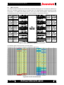
1
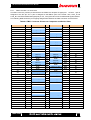
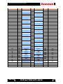
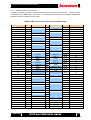
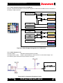
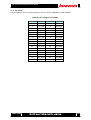
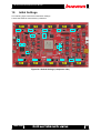
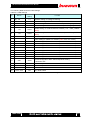
TB-6V-LX760-LSI Hardware User Manual TB-6V-LX760-LSI Hardware User Manual Rev.3.00 Rev.3.00 1 TB-6V-LX760-LSI Hardware User Manual Revision History Version Date Description Rev.1.xx 2009/xx/xx Preliminary Rev.2.00 2010/05/06 Initial release Rev.2.01 2010/06/25 -Added J66, J53 to figure 12-1 Publisher Sen Odajima Yoshioka -Modified table 12-1 Added J66,J53 Separate SW5,SW6 Changed initial settings : No1, 6 ,7 ,18, 20.21 Rev.2.02 2010/07/07 - Modified table 6-1, table 6-2, table 6-3 Yoshioka - Modified figure 6-1, figure 7-3 - Delete wrong information on 8-3 FMC connector - Modified explaining of clock signal of each FMC connectors - Modified figure 9-1 - Add DIP SW pin number on table 9-1 and 9-2 - Changed connector for FAN on 6.5 Power supply for FAN Rev.2.03 2012/04/24 -Modified Q’ty of TB-FMCH-STACK and Yoshioka Q’ty of TB-FMCH-CONNECTRO Rev.3.00 2012/07/17 - Modified revision of pin assign table Yoshioka - Modified PCB dimension and surface coating - Modified External view - Modified Table 8-1 LA06_P/N, LA33_P/N, CLK1_M2C_P/N and CLK0_M2C_P/N - Add comment to Table 8-1, 8-2, 8-6, 8-7: LA33_P/N. these are not differential pair - Modified Table 8-2 LA15_P/N, LA19_P/N, LA33_P/N, CLK1_M2C_P/N and CLK0_M2C_P/N - Modified Table 8-4 CLK1_M2C_P/N and CLK0_M2C_P/N - Modified Table 8-5 CLK1_M2C_P/N and CLK0_M2C_P/N - Modified Table 8-6 LA11_P/N, LA33_P/N, CLK1_M2C_P/N and CLK0_M2C_P/N - Modified Table 8-7 CLK1_M2C_P/N and CLK0_M2C_P/N - Modified Table 8-8 CLK1_M2C_P/N and CLK0_M2C_P/N - Modified Table 8-9 CLK1_M2C_P/N and CLK0_M2C_P/N - Modified Table 8-10 CLK1_M2C_P/N and CLK0_M2C_P/N - Modified Figure 1-3 Power Supply Arrangement for FPGA Banks - Modified Spec of FAN - Added 11-4 Pin header and Table 11-4 pin assign of pin header - Modified Figure 12-1 Default settings - Modified Table 12-1 Initial Settings (removed J66) Rev.3.00 2 TB-6V-LX760-LSI Hardware User Manual Table of Contents 1. 2. 3. 4. 5. Related Documents and Accessories ......................................................................................... 9 Overview ...................................................................................................................................... 9 Feature ........................................................................................................................................ 9 Block Diagram ............................................................................................................................11 External View of the Board ........................................................................................................ 12 5.1. TB-6V-LX760-LSI .................................................................................................................... 12 5.2. TB-FMCH-STACK and TB-FMCH-CONNECTOR ................................................................... 13 6. Board Specifications .................................................................................................................. 14 6.1. TB-6V-LX760-LSI Board Structure .......................................................................................... 14 6.2. TB-FMCH-STACK Board Structure ......................................................................................... 14 6.3. TB-FMCH-CONNECTER Board Structure .............................................................................. 15 6.4. Layout of TB-6V-LX760-LSI Board Components .................................................................... 16 6.5. Layout of the TB-FMCH-STACK Board Components ............................................................. 17 6.6. Layout of the TB-FMCH-CONNECTER Board Components .................................................. 17 7. Description of Components ....................................................................................................... 18 7.1. DDR3 SDRAM ......................................................................................................................... 18 7.2. SPI FLASH .............................................................................................................................. 19 7.3. BPI FLASH .............................................................................................................................. 19 7.4. MicroSD/NAND FLASH (these are only for Virtex-6 configuration) ........................................ 20 8. Interfaces ................................................................................................................................... 21 8.1. USB and I2C ............................................................................................................................ 21 8.2. Method of Rewriting an EEPROM for USB PHY ..................................................................... 21 8.3. FMC Connector ....................................................................................................................... 22 9. 8.3.1. FMC1 LPC MC / CC Connector ...................................................................................... 23 8.3.2. FMC2 LPC MC / CC Connector ...................................................................................... 25 8.3.3. FMC3 LPC MC / CC Connector ...................................................................................... 27 8.3.4. FMC4 LPC MC / CC Connector ...................................................................................... 29 8.3.5. FMC5 LPC MC / CC Connector ...................................................................................... 31 8.3.6. FMC6 LPC MC / CC Connector ...................................................................................... 33 8.3.7. FMC7 LPC MC / CC Connector ...................................................................................... 35 8.3.8. FMC8 LPC MC / CC Connector ...................................................................................... 37 8.3.9. FMC9 LPC MC / CC Connector ...................................................................................... 39 8.3.10. FMC10 LPC MC / CC Connector .................................................................................... 41 Clock System Diagram .............................................................................................................. 45 9.1. 10. PLL Setting .............................................................................................................................. 46 Power Supply System ........................................................................................................... 48 10.1. Power Consumption Estimation .......................................................................................... 48 10.2. Power Supply System Diagram ........................................................................................... 49 10.3. Power Supply Monitor ......................................................................................................... 50 10.4. Power Supply Arrangement for FPGA Banks ...................................................................... 51 10.5. Power Supply for Fan .......................................................................................................... 51 Rev.3.00 3 TB-6V-LX760-LSI Hardware User Manual 11. LED/SW/JUMPER ................................................................................................................ 52 11.1. LED .......................................................................................................................................... 52 11.2. Switch ...................................................................................................................................... 53 11.3. JUMPER .................................................................................................................................. 54 11.4. Pin Header ............................................................................................................................... 55 12. Initial Settings ........................................................................................................................ 56 List of Figures Figure4-1 Block Diagram ..................................................................................................................11 Figure5-1 Component Side .............................................................................................................. 12 Figure5-3 External view of the TB-FMCH-STACK and TB-FMCH-CONNECTOR .......................... 13 Figure6-1 Layout of TB-6V-LX760-LSI Board Components ............................................................. 16 Figure6-2 Layout of the TB-FMCH-STACK Board Components ...................................................... 17 Figure6-3 Layout of the TB-FMCH-CONNECTER Board Components........................................... 17 Figure7-1 DDR3 Peripheral Connections......................................................................................... 18 Figure7-2 SPI Flash Peripheral Connections ................................................................................... 19 Figure7-3 BPI Flash Peripheral Connections ................................................................................... 19 Figure7-4 CONFIG Peripheral Connections .................................................................................... 20 Figure7-5 JTAG Chain...................................................................................................................... 20 Figure8-1 USB and I2C Peripheral Connections ............................................................................. 21 Figure8-2 FMC Connector Peripheral Connections ......................................................................... 22 Figure8-3 Low-Pin Count Pinouts .................................................................................................... 22 Figure8-4 SDA,SCL,GA1/0 TDI/TDO Circuit.................................................................................... 43 Figure8-5 PG_C2M Circuit ............................................................................................................... 43 Figure8-6 VREF_A_M2C Circuit ...................................................................................................... 43 Figure8-7 FMC_VREF Select Circuit ............................................................................................... 44 Figure8-8 VADJ Circuit ..................................................................................................................... 44 Figure9-1 Clock System Diagram .................................................................................................... 45 Figure10-1 Power Supply System Diagram ..................................................................................... 49 Figure10-2 Power Supply Monitor .................................................................................................... 50 Figure10-3 Power Supply Arrangement for FPGA Banks ................................................................ 51 Figure10-4 Fan Connector Peripheral Circuit .................................................................................. 51 Figure12-1 Default Settings (component side) ................................................................................ 56 Rev.3.00 4 TB-6V-LX760-LSI Hardware User Manual List of Tables Table6-1 TB-6V-LX760-LSI Board Structure .................................................................................... 14 Table6-2 TB-FMCH-STACK Board Structure ................................................................................... 14 Table6-3 TB-FMCH-CONNECTER Board Structure ........................................................................ 15 Table8-1 FMC1 Connector Pinouts on Component and Solder Sides ............................................. 23 Table8-2 FMC2 Connector Pinouts on Component and Solder Sides ............................................. 25 Table8-3 FMC3 Connector Pinouts on Component and Solder Sides ............................................. 27 Table8-4 FMC4 Pinouts on Component and Solder Sides .............................................................. 29 Table8-5 FMC5 Pinouts on Component and Solder Sides .............................................................. 31 Table8-6 FMC6 Connector Pinouts on Component and Solder Sides ............................................. 33 Table8-7 FMC7 Connector Pinouts on Component and Solder Sides ............................................. 35 Table8-8 FMC8 Connector Pinouts on Component and Solder Sides ............................................. 37 Table8-9 FMC9 Connector Pinouts on Component and Solder Sides ............................................. 39 Table8-10 FMC10 Connector Pinouts on Component and Solder Sides ......................................... 41 Table9-1 PLL’s M Divide Setting Table ............................................................................................. 46 Table9-2 PLL’s N Divide Setting Table ............................................................................................. 47 Table11-1 LED Functions ................................................................................................................. 52 Table11-2 Switch Functions.............................................................................................................. 53 Table11-3 Jumper Functions ............................................................................................................ 54 Table11-4 Pin assign of Pin header .................................................................................................. 55 Table12-1 Initial Settings .................................................................................................................. 57 Rev.3.00 5 TB-6V-LX760-LSI Hardware User Manual Introduction Thank you for purchasing the TB-6V-LX760-LSI board. Before using the product, be sure to carefully read this user manual and fully understand how to correctly use the product. First read through this manual, and then always keep it handy. SAFETY PRECAUTIONS Be sure to observe these precautions Observe the precautions listed below to prevent injuries to you, other personnel or damage to property. Before using the product, read these safety precautions carefully to assure safe use. These precautions contain serious safety instructions that must be observed. After reading through this manual, be sure to always keep it handy. The following conventions are used to indicate the possibility of injury/damage and classify precautions if the product is handled incorrectly. Danger Indicates the high possibility of serious injury or death if the product is handled incorrectly. Indicates the possibility of serious injury or death if the product is handled Warning incorrectly. Indicates the possibility of injury or physical damage in connection with property if Caution the product is handled incorrectly. The following graphical symbols are used to indicate and classify precautions in this manual. (Examples) Turn off the power switch. Do not disassemble the product. ! Rev.3.00 Do not attempt this. 6 TB-6V-LX760-LSI Hardware User Manual Warning In the event of a failure, disconnect the power supply. If the product is used as is, a fire or electric shock may occur. Disconnect the power supply immediately and contact technical support. If an unpleasant smell or smoking occurs, disconnect the power supply. If the product is used as is, a fire or electric shock may occur. immediately. Disconnect the power supply After verifying that no smoking is observed, contact our sales personnel for repair. Do not disassemble, repair or modify the product. Otherwise, a fire or electric shock may occur due to a short circuit or heat generation. For inspection, modification or repair, contact our sales personnel. ! Do not touch a cooling fan. As a cooling fan rotates at high speed, do not put your hand close to it or touch it. Otherwise, it may cause injury. ! Do not place the product in an unstable position. Otherwise, it may drop or fall, resulting in injury to persons or failure. ! If the product is dropped or damaged, do not use it as is. ! Do not touch the product with a metallic object. ! Do not place the product in dusty or humid locations or where water may Otherwise, a fire or electric shock may occur. Otherwise, a fire or electric shock may occur. splash on it. Otherwise, a fire or electric shock may occur. ! Do not get the product wet or touch it with a wet hand. Otherwise, the product may be damaged and break down or it may cause a fire or electric shock. ! Do not touch a connector on the product (gold-plated portion). Otherwise, the surface of a connector may be contaminated with sweat or skin oil, resulting in contact failure of a connector or it may cause a malfunction, fire or electric shock due to static electricity. Rev.3.00 7 TB-6V-LX760-LSI Hardware User Manual Caution Do not use or place the product in the following locations. ! Humid and dusty locations Airless locations such as closet or bookshelf Locations which receive oily smoke or steam Locations exposed to direct sunlight Locations close to heating equipment Closed inside of a car where the temperature becomes high Static locations Locations close to water or chemicals Otherwise, a fire, electric shock, accident or deformation may occur due to a short circuit or heat generation. ! Do not place heavy things on the product. Otherwise, the product may be damaged. ■ Disclaimer This product is a Xilinx Virtex6 FPGA evaluation board. Tokyo Electron Device Limited assumes no responsibility for any damages resulting from the use of this product for purposes other than those stated. Even if the product is used properly, Tokyo Electron Device Limited assumes no responsibility for any damages caused by: (1) Earthquake, thunder, natural disaster or fire resulting from the use beyond our responsibility, acts by a third party or other accidents, the customer’s willful or accidental misuse or use under other abnormal conditions. (2) Secondary impact arising from use of this product or its unusable state (business interruption or others) (3) Use of this product against the instructions given in this manual. (4) Malfunctions due to connection to other devices. Tokyo Electron Device Limited assumes no responsibility or liability for: (1) Erasure or corruption of data arising from use of this product. (2) Any consequences or other abnormalities arising from use of this product, or (3) Damage of this product not due to our responsibility or failure due to modification This product has been developed for research, testing or evaluation. It is not authorized for use in any system or application that requires high reliability. Repair of this product is carried out by replacing it on a chargeable basis, not repairing the faulty devices. However, non-chargeable replacement is offered for initial failure if such notification is received within two weeks after delivery of the product. The specification of this product is subject to change without prior notice. The product is subject to discontinuation without prior notice. Rev.3.00 8 TB-6V-LX760-LSI Hardware User Manual 1. Related Documents and Accessories Related documents: All documents relating to this board can be downloaded from our website. Please see attached “Welcome latter” on the products. Board accessories: - FMC spacer set 2. Overview This document describes the design specification of the TB-6V-LX760-LSI board. The design covers the TB-6V-LX760-LSI board and two FMC option boards (TB-FMCH-STACK and TB-FMCH-CONNECTOR). 3. Feature FPGA Devices : XC6VLX760-2FFG1760 : XC3S700AN-4FGG484C (It is only for Virtex-6 Configuration) DDR3 SDRAM CH1 : 1Gbit (8Meg x 16bit x 8Bank) x 2 DDR3 SDRAM CH2 : 1Gbit (8Meg x 16bit x 8Bank) x 2 NAND FLASH : 4G (16bit) x 1 (for FPGA Configuration) SPI Flash : 64MBit x 1 (for MicroBlaze) BPI Flash : 256MBit x 1 (for test) FMC (LPC) : Connectors for component side x 10 FMC (LPC) : Connectors for solder side x 10 USB : Type B Hi-speed USB (target) SD CARD : MicroSD (It is only for Virtex-6 Configuration) Expansion Connector : x 1 (30-bit) connecting to XC6VLX760 Memory Interface Others LTC2978CUP : Onboard power source monitor Clock : OSC 24MHz for USB (mounted) : 50MHz for XC3S700AN (mounted) : 266MHz for DDR3 (mounted) : 16MHz for PLL (mounted) I2C : 4pin Header FAN : 3pin Header connecting to XC3S700AN LED : Green color LED for XC6VLX760 configuration DONE : 14 general purpose green color LEDs connecting to XC6VLX760 : 2 general purpose red LEDs connecting to XC6VLX760 : Green color LED for XC3S700AN configuration DONE : 3 general purpose red LEDs connected to XC3S700AN : Pushbutton switch to initiate configuration : General purpose 16-bit DIP switch connected to XC6VLX760 SW Rotary SW Rev.3.00 : General purpose 4-bit pushbutton switch connected to XC6VLX760 : 2 switches connected to XC3S700AN 9 TB-6V-LX760-LSI Hardware User Manual Power Supply: The +12 volt power supply can be derived either from the Molex 39-29-1048 connector or from the 39-30-0060. A dedicated power supply is attached. Onboard power supply module: Various Linear modules (LTM4601A, LTM4606, LTM8025 etc.) Holes for fixing an FPGA radiator, dedicated heat sink and FAN Spacers and screws for attaching option boards 5 TB-FMCH-STACK boards and 3 TB-FMCH-CONNECTERs Warning Virtex-6 FPGA does not support 3.3V IO. Rev.3.00 10 TB-6V-LX760-LSI Hardware User Manual 4. Block Diagram The following figure represents the block diagram of the TB-6V-LX760-LSI and illustrates the assignment of various blocks and connectors to IO banks on the FPGA. Figure4-1 Block Diagram Rev.3.00 11 TB-6V-LX760-LSI Hardware User Manual 5. External View of the Board 5.1. TB-6V-LX760-LSI Figure5-1 Component Side FMC Connector6 (Module Low Pin) FMC Connector1 (Module Low Pin) FMC Connector7 (Module Low Pin) FMC Connector2 (Module Low Pin) FMC Connector8 (Module Low Pin) FMC Connector3 (Module Low Pin) FMC Connector9 (Module Low Pin) FMC Connector10 (Module Low Pin) FMC Connector4 (Module Low Pin) FMC Connector5 (Module Low Pin) Figure5-2 Solder Side Rev.3.00 12 TB-6V-LX760-LSI Hardware User Manual 5.2. TB-FMCH-STACK and TB-FMCH-CONNECTOR The TB-FMCH-STACK and the TB-FMCH-CONNECTOR permit the interconnection of multiple TB-6V-LX760T-LSI boards in either a horizontal or vertical configuration. TB-FMCH-Connector Solder side Figure5-3 External view of the TB-FMCH-STACK and TB-FMCH-CONNECTOR Rev.3.00 13 TB-6V-LX760-LSI Hardware User Manual 6. Board Specifications 6.1. TB-6V-LX760-LSI Board Structure The following table shows the board structure and the specifications. For details about connector locations, refer to the board layout drawing. For details about clock structure and operational frequency, refer to the clock system diagram. Table6-1 TB-6V-LX760-LSI Board Structure Item Category-I Category-II Specification 1 Number of Layers 16 2 Dimensions 369mm x 225mm Thickness 3mm 4 Resist Color Red 5 Material FR-4 3 Board Structure 6 Component Side Height 7 8 9 13.0mm (without FAN and power connector) Solder Side 7.1mm Single Signal 50 Ohm Differential Signal 90 Ohm, 100 Ohm Impedance Control 10 RoHS/Pbfree RoHS/Pbfree RoHS, lead-free solder 11 Surface Coating - Gold plating 6.2. Remarks TB-FMCH-STACK Board Structure The following table shows the board structure and the specifications. For details about connector locations, refer to the board layout drawing. Table6-2 TB-FMCH-STACK Board Structure Item Category-II Specification 1 Number of Layers 16 2 Dimensions 69mm x 40mm Thickness 3mm 4 Resist Color Red 5 Material FR-4 Component Side 6.5mm 3 6 7 8 Category-I Board Structure Height Impedance Control 9 Solder Side 7.1mm Single Signal 50 Ohm Differential Signal 100 Ohm 10 RoHS/Pbfree RoHS/Pbfree RoHS, lead-free solder 11 Surface Coating - Gold plating Rev.3.00 Remarks 14 TB-6V-LX760-LSI Hardware User Manual 6.3. TB-FMCH-CONNECTER Board Structure The following table shows the board structure and the specifications. For details about connector locations, refer to the board layout drawing. Table6-3 TB-FMCH-CONNECTER Board Structure Item Category-II Specification 1 Number of Layers 16 2 Dimensions 69mm x 80mm Thickness 3mm Resist Color Red 5 Material FR-4 6 Component Side 2mm Solder Side 7.1mm Single Signal 50 Ohm Differential Signal 100 Ohm 3 Category-I Board Structure 4 7 8 Height Impedance Control 9 10 RoHS/Pbfree RoHS/Pbfree RoHS, lead-free solder 11 Surface Coating - Gold plating Rev.3.00 Remarks 15 TB-6V-LX760-LSI Hardware User Manual 6.4. Layout of TB-6V-LX760-LSI Board Components The following figure shows the dimensions of the TB-6V-LX760-LSI. 225 112.5 Unit : mm 15.5 12.5 ATX CN ATX CN 15.5 5.0 8.0 Ф6.0 Ф2.7 DC-DC Regulato r DC-DC Regulato r LED OUT 70.0 LTC2 978 A01 DC-DC Regulato r FMC 1 DC-DC Regulato r LED OUT FMC 6 44.5 A01 DC-DC Regulato r A01 DC-DC Regulato r DC-DC Regulato r LED OUT FAN CN A01 LED OUT 70.0 FMC 2 DC-DC Regulato r FMC 7 DC-DC Regulato r 3 A01 FMC 3 69 31. 5 LED OUT A01 FMC 8 LED OUT XC6VSX760T-1 FF1760 (42.5x42.5) JS28F256 31. 5 3 3 1 A01 DDR 3 FMC 4 LED OUT FMC 9 DDR 3 DDR 3 DDR 3 31. 5 DC-DC Regulato r A01 31. 5 3 A01 FMC 10 31.5 44.5 CY7C68013A -56PVXC 149.5 LED OUT 112.5 MicroSD 5.0 2908-05WB-MG USB 8.0 XR2A-0811-N LED OUT 369 50MHz OSC SN74CB3 T3245PW SN74CB3 T3245PW SN74CB3 T3245PW SN74CB3 T3245PW XC3S700AN -FG484 23*23 MT29F4G16 BABWP A01 FMC 5 70.0 LED OUT 219.5 69 Figure6-1 Layout of TB-6V-LX760-LSI Board Components Rev.3.00 16 TB-6V-LX760-LSI Hardware User Manual 6.5. Layout of the TB-FMCH-STACK Board Components The following figure shows the dimensions of the TB-FMCH-STACK board and locations of its connectors. Figure6-2 Layout of the TB-FMCH-STACK Board Components 6.6. Layout of the TB-FMCH-CONNECTER Board Components The following figure shows the dimensions of the TB-FMCH-CONNECTER board and locations of its connectors. Figure6-3 Layout of the TB-FMCH-CONNECTER Board Components Rev.3.00 17 TB-6V-LX760-LSI Hardware User Manual 7. Description of Components 7.1. DDR3 SDRAM The TB-6V-LX760-LSI board has four DDR3 SDRAM chips. Device: MT41J64M16LA-15E:B (Micron) 1-Gbit (8Meg x 16bit x 8Bank) x 4 or equivalents The DDR3 memory device can be divided into two groups as shown in following figure. GroupA DM[3:2] DDR3-SDRAM 1Gbit [MT41J64M16LA-15] A[13:0], BA[2:0], CK, XCK, CKE, XCS, ODT, XWE, XRAS, XCAS, XRESET DQ[31:16], DQS[3:2], XDQS[3:2] DM[1:0] DDR3-SDRAM 1Gbit DQ[15:0], [MT41J64M16LA-15] DQS[1:0], XDQS[1:0] FPGA [XC6VLX760-FFG1760C] GroupB DM[3:2] DDR3-SDRAM 1Gbit [MT41J64M16LA-15] A[13:0], BA[2:0], CK, XCK, CKE, XCS, ODT, XWE, XRAS, XCAS, XRESET DQ[31:16], DQS[3:2], XDQS[3:2] DM[1:0] DDR3-SDRAM 1Gbit DQ[15:0], [MT41J64M16LA-15] DQS[1:0], XDQS[1:0] Figure7-1 DDR3 Peripheral Connections Rev.3.00 18 TB-6V-LX760-LSI Hardware User Manual 7.2. SPI FLASH The TB-6V-LX760-LSI board has one SPI Flash memory device. Device: M25P64-VMF6TP (Numonyx) 64-MBit Figure7-2 SPI Flash Peripheral Connections 7.3. BPI FLASH The TB-6V-LX760-LSI board has one BPI Flash memory device. Device: JS28F256P30TF (Numonyx) 256-MBit Figure7-3 BPI Flash Peripheral Connections Rev.3.00 19 TB-6V-LX760-LSI Hardware User Manual 7.4. MicroSD/NAND FLASH (these are only for Virtex-6 configuration) The TB-6V-LX760-LSI board has one NAND Flash for storing Virtex-6 configuration files and one MicroSD socket. The Spartan-3AN reads the data stored in the Micro SD/NAND Flash memory device to configure the Virtex-6 device. Device: NAND Flash: MT29F4G16BABWP (Micron) 4-G (16-bit) For more information, refer to the related document “Configuration Method Using SD and XC3S700AN” NMT (uSD_CONF_UserManual_V6LSI_x.xxe.pdf). Figure7-4 CONFIG Peripheral Connections The following figure shows the JTAG chain of Virtex-6 and Spartan-3AN. The Spartan-3AN comes with burned ROM data for configuration. No need to change it, if it is used in an ordinary way. Figure7-5 JTAG Chain Rev.3.00 20 TB-6V-LX760-LSI Hardware User Manual 8. Interfaces 8.1. USB and I2C USB Connector Type B: 67068-8000 USB PHY: CY7C68013A-56PVXC I2C Connector Pin Header: A2-2PA-2.54DSA Figure8-1 USB and I2C Peripheral Connections 8.2. Method of Rewriting an EEPROM for USB PHY Free software “EzMr.exe” is available from Cypress Semiconductor Corporation for rewriting the CY7C68013 EEPROM. The following procedure describes how to rewrite an EEPROM. (Contact Cypress Semiconductor for more information if necessary.) 1. Remove the J53 jumper 2. Connect the board to a PC using a USB cable. 3. Run EzMr.exe. 4. Reinstall jumper J53. 5. On the EzMr.exe panel select the EEPROM Erase File (.hex) to erase the EEPROM data. 6. After completion of downloading, disconnect the USB cable. 7. Connect it again to get the PC to recognize the board once more. 8. On the EzMr.exe panel select the target firm binary data (.iic) and download it. 9. Again, disconnect and reconnect the USB cable to get the PC recognize it. 10. That’s all. Rev.3.00 21 TB-6V-LX760-LSI Hardware User Manual 8.3. FMC Connector The TB-6V-LX760-LSI board has 10 FMC LPC connectors (Carrier type) on its component side and 10 FMC LPC connectors (Module type) on its solder side. The following figure shows the FPGA to FMC connections. For details about FPGA pinouts, refer to the board circuit diagram. A Microsoft Excel spreadsheet document, defining the pinouts, is also available as a published reference. Figure8-2 FMC Connector Peripheral Connections The following figure shows the FMC connector pinout. Note that not all LPC (Low-Pin Count) are connected to the FPGA. Figure8-3 Low-Pin Count Pinouts Rev.3.00 22 TB-6V-LX760-LSI Hardware User Manual 8.3.1. FMC1 LPC MC / CC Connector The FMC connector (J43/J67) is interfaced to the FPGA over 36 pairs of signal pins. Of them, 1 pair is assigned to the GC pin and 1 pair is assigned to the MRCC pins of the FPGA. Also, LA33_P and LA33_N is not FPGA deferential signal pair pin. So, LA33_P/N cannot use for differential signal interface. The following table shows the pin mapping assignments between the FMC connector and the FPGA. Table8-1 FMC1 Connector Pinouts on Component and Solder Sides Bank No. Pin No. 26 26 P25 R25 25 25 D38 C38 25 25 G34 H33 26 26 K30 J31 26 26 G33 G32 Rev.3.00 C GND DP0_C2M_P DP0_C2M_N GND GND DP0_M2C_P DP0_M2C_N GND GND LA06_P LA06_N GND GND LA10_P LA10_N GND GND LA14_P LA14_N GND GND LA18_P_CC LA18_N_CC GND GND LA27_P LA27_N GND GND *1 SCL *1 SDA GND GND *2 GA0 *7 12P0V GND *7 12P0V GND *7 3P3V GND 1 2 3 4 5 6 7 8 9 10 11 12 13 14 15 16 17 18 19 20 21 22 23 24 25 26 27 28 29 30 31 32 33 34 35 36 37 38 39 40 D PinNo. * 4 PG_C2M GND GND GBTCLK0_M2C_P GBTCLK0_M2C_N GND GND LA01_P_CC A39 LA01_N_CC B38 GND LA05_P H35 LA05_N H34 GND LA09_P D35 LA09_N E34 GND LA13_P C35 LA13_N B34 GND LA17_P_CC M29 LA17_N_CC N28 GND LA23_P C33 LA23_N D32 GND LA26_P A36 LA26_N B36 GND *3 TCK *3 TDI *3 TDO *7 3P3VAUX *3 TMS *3 TRST_L *2 GA1 *7 3P3V GND *7 3P3V GND *7 3P3V Bank No. 26 26 26 26 25 25 25 25 26 26 25 25 25 25 23 TB-6V-LX760-LSI Hardware User Manual Bank No. 25 25 Pin No. N31 M32 25 25 N30 P31 25 25 G36 F36 25 25 B37 A37 26 26 B33 C34 25 25 P30 N29 26 26 E32 F32 26 26 M28 L29 26 26 L27 M27 25 25 R28 P28 26 26 P27 R27 25 25 K33 L31 Rev.3.00 G GND CLK1_M2C_P CLK1_M2C_N GND GND LA00_P_CC LA00_N_CC GND LA03_P LA03_N GND LA08_P LA08_N GND LA12_P LA12_N GND LA16_P LA16_N GND LA20_P LA20_N GND LA22_P LA22_N GND LA25_P LA25_N GND LA29_P LA29_N GND LA31_P LA31_N GND LA33_P LA33_N GND *7 VADJ GND 1 2 3 4 5 6 7 8 9 10 11 12 13 14 15 16 17 18 19 20 21 22 23 24 25 26 27 28 29 30 31 32 33 34 35 36 37 38 39 40 H Pin No. *5 VREF_A_M2C *6 PRSNT_M2C_L G31 GND CLK0_M2C_P D33 CLK0_M2C_N E33 GND LA02_P M31 LA02_N L32 GND LA04_P F34 LA04_N F35 GND LA07_P F37 LA07_N E37 GND LA11_P C36 LA11_N D37 GND LA15_P K32 LA15_N J32 GND LA19_P H29 LA19_N H30 GND LA21_P K28 LA21_N J28 GND LA24_P A35 LA24_N A34 GND LA28_P P26 LA28_N N26 GND LA30_P A32 LA30_N B32 GND LA32_P F31 LA32_N F30 GND *7 VADJ Bank No. 26 26 26 25 25 25 25 25 25 25 25 25 25 26 26 26 26 26 26 26 26 26 26 26 26 24 TB-6V-LX760-LSI Hardware User Manual 8.3.2. FMC2 LPC MC / CC Connector The FMC connector (J44/J68) is interfaced to the FPGA over 36 pairs of signal pins. Of them, 2 pairs are assigned to the MRCC pins of the FPGA. Also, LA33_P and LA33_N is not FPGA deferential signal pair pin. So, LA33_P/N cannot use for differential signal interface. The following table shows the pin mapping assignments between the FPC connector and the FPGA. Table8-2 FMC2 Connector Pinouts on Component and Solder Sides Bank No. Pin No. 16 16 J40 K39 17 17 G37 H36 17 17 H39 G39 16 16 L42 L41 17 17 C41 C40 Rev.3.00 C GND DP0_C2M_P DP0_C2M_N GND GND DP0_M2C_P DP0_M2C_N GND GND LA06_P LA06_N GND GND LA10_P LA10_N GND GND LA14_P LA14_N GND GND LA18_P_CC LA18_N_CC GND GND LA27_P LA27_N GND GND *1 SCL *1 SDA GND GND *2 GA0 *7 12P0V GND *7 12P0V GND *7 3P3V GND 1 2 3 4 5 6 7 8 9 10 11 12 13 14 15 16 17 18 19 20 21 22 23 24 25 26 27 28 29 30 31 32 33 34 35 36 37 38 39 40 D PinNo. *4 PG_C2M GND GND GBTCLK0_M2C_P GBTCLK0_M2C_N GND GND LA01_P_CC T31 LA01_N_CC T32 GND LA05_P N33 LA05_N P32 GND LA09_P P33 LA09_N N34 GND LA13_P J36 LA13_N K35 GND LA17_P_CC J42 LA17_N_CC H41 GND LA23_P F41 LA23_N E42 GND LA26_P D42 LA26_N D41 GND *3 TCK *3 TDI *3 TDO *7 3P3VAUX *3 TMS *3 TRST_L *2 GA1 *7 3P3V GND *7 3P3V GND *7 3P3V Bank No. 16 16 17 17 17 17 17 17 16 16 17 17 17 17 25 TB-6V-LX760-LSI Hardware User Manual Bank No. 16 16 Pin No. M38 M37 16 16 M36 N35 16 16 U33 T34 17 17 K37 L36 17 17 L35 M34 17 17 K34 J35 16 16 K42 J41 16 16 G42 F42 16 16 H40 G41 17 17 B41 B42 17 17 E39 E38 16 16 U31 M39 Rev.3.00 G GND CLK1_M2C_P CLK1_M2C_N GND GND LA00_P_CC LA00_N_CC GND LA03_P LA03_N GND LA08_P LA08_N GND LA12_P LA12_N GND LA16_P LA16_N GND LA20_P LA20_N GND LA22_P LA22_N GND LA25_P LA25_N GND LA29_P LA29_N GND LA31_P LA31_N GND LA33_P LA33_N GND *7 VADJ GND 1 2 3 4 5 6 7 8 9 10 11 12 13 14 15 16 17 18 19 20 21 22 23 24 25 26 27 28 29 30 31 32 33 34 35 36 37 38 39 40 H Pin No. *5 VREF_A_M2C *6 PRSNT_M2C_L D40 GND CLK0_M2C_P J38 CLK0_M2C_N J37 GND LA02_P L40 LA02_N K40 GND LA04_P K38 LA04_N L37 GND LA07_P R33 LA07_N R32 GND LA11_P M33 LA11_N L34 GND LA15_P A41 LA15_N A40 GND LA19_P F40 LA19_N F39 GND LA21_P P38 LA21_N P37 GND LA24_P R34 LA24_N P35 GND LA28_P P36 LA28_N N36 GND LA30_P T35 LA30_N R35 GND LA32_P B39 LA32_N C39 GND *7 VADJ Bank No. 17 17 17 16 16 16 16 16 16 17 17 17 17 17 17 16 16 16 16 16 16 16 16 17 17 26 TB-6V-LX760-LSI Hardware User Manual 8.3.3. FMC3 LPC MC / CC Connector The FMC connector (J45/J69) is interfaced to the FPGA over 36 pairs of signal pins. are assigned to the MRCC pins of the FPGA. Of them, 2 pairs The following table shows the pin mapping assignments between the FMC connector and the FPGA. Table8-3 FMC3 Connector Pinouts on Component and Solder Sides Bank No. Pin No. 15 15 U37 T37 14 14 Y35 Y34 15 15 R40 P40 14 14 V41 W40 14 14 AA40 Y40 Rev.3.00 C GND DP0_C2M_P DP0_C2M_N GND GND DP0_M2C_P DP0_M2C_N GND GND LA06_P LA06_N GND GND LA10_P LA10_N GND GND LA14_P LA14_N GND GND LA18_P_CC LA18_N_CC GND GND LA27_P LA27_N GND GND *1 SCL *1 SDA GND GND *2 GA0 *7 12P0V GND *7 12P0V GND *7 3P3V GND 1 2 3 4 5 6 7 8 9 10 11 12 13 14 15 16 17 18 19 20 21 22 23 24 25 26 27 28 29 30 31 32 33 34 35 36 37 38 39 40 D PinNo. *4 PG_C2M GND GND GBTCLK0_M2C_P GBTCLK0_M2C_N GND GND LA01_P_CC Y38 LA01_N_CC Y37 GND LA05_P U41 LA05_N V40 GND LA09_P AD33 LA09_N AD32 GND LA13_P AC33 LA13_N AB32 GND LA17_P_CC AB34 LA17_N_CC AA34 GND LA23_P AB41 LA23_N AC40 GND LA26_P W38 LA26_N W37 GND *3 TCK *3 TDI *3 TDO *7 3P3VAUX *3 TMS *3 TRST_L *2 GA1 *7 3P3V GND *7 3P3V GND *7 3P3V Bank No. 14 14 15 15 14 14 14 14 14 14 14 14 15 15 27 TB-6V-LX760-LSI Hardware User Manual Bank No. Pin No. 15 15 V38 U38 14 14 AC38 AC39 14 14 AA39 Y39 15 15 U42 T42 15 15 T40 T39 15 15 Y32 Y33 14 14 AA32 AB33 15 15 W32 W33 14 14 AA41 Y42 15 15 N41 N40 15 15 W35 W36 15 15 M42 M41 Rev.3.00 G GND CLK1_M2C_P CLK1_M2C_N GND GND LA00_P_CC LA00_N_CC GND LA03_P LA03_N GND LA08_P LA08_N GND LA12_P LA12_N GND LA16_P LA16_N GND LA20_P LA20_N GND LA22_P LA22_N GND LA25_P LA25_N GND LA29_P LA29_N GND LA31_P LA31_N GND LA33_P LA33_N GND *7 VADJ GND 1 2 3 4 5 6 7 8 9 10 11 12 13 14 15 16 17 18 19 20 21 22 23 24 25 26 27 28 29 30 31 32 33 34 35 36 37 38 39 40 H Pin No. *5 VREF_A_M2C *6 PRSNT_M2C_L AB42 GND CLK0_M2C_P AB37 CLK0_M2C_N AA37 GND LA02_P AB39 LA02_N AB38 GND LA04_P AD42 LA04_N AC41 GND LA07_P AA36 LA07_N AA35 GND LA11_P AC34 LA11_N AC35 GND LA15_P P41 LA15_N P42 GND LA19_P V35 LA19_N V34 GND LA21_P R37 LA21_N T36 GND LA24_P V36 LA24_N U36 GND LA28_P W41 LA28_N W42 GND LA30_P U34 LA30_N V33 GND LA32_P R39 LA32_N R38 GND *7 VADJ Bank No. 14 14 14 14 14 14 14 14 14 14 14 15 15 15 15 15 15 15 15 14 14 15 15 15 15 28 TB-6V-LX760-LSI Hardware User Manual 8.3.4. FMC4 LPC MC / CC Connector The FMC connector (J46/J70) is interfaced to the FPGA over 36 pairs of signal pins. are assigned to the MRCC pins of the FPGA. Of them, 2 pairs The following table shows the pin mapping assignments between the FMC connector and the FPGA. Table8-4 FMC4 Pinouts on Component and Solder Sides Bank No. Pin No. 12 12 AW42 AV41 12 12 AT42 AU42 13 13 AJ40 AH40 13 13 AL42 AK42 13 13 AJ41 AJ42 Rev.3.00 C GND DP0_C2M_P DP0_C2M_N GND GND DP0_M2C_P DP0_M2C_N GND GND LA06_P LA06_N GND GND LA10_P LA10_N GND GND LA14_P LA14_N GND GND LA18_P_CC LA18_N_CC GND GND LA27_P LA27_N GND GND *1 SCL *1 SDA GND GND *2 GA0 *7 12P0V GND *7 12P0V GND *7 3P3V GND 1 2 3 4 5 6 7 8 9 10 11 12 13 14 15 16 17 18 19 20 21 22 23 24 25 26 27 28 29 30 31 32 33 34 35 36 37 38 39 40 D PinNo. *4 PG_C2M GND GND GBTCLK0_M2C_P GBTCLK0_M2C_N GND GND LA01_P_CC AV40 LA01_N_CC AW41 GND LA05_P AT40 LA05_N AR40 GND LA09_P AR42 LA09_N AP42 GND LA13_P AP41 LA13_N AN40 GND LA17_P_CC AG36 LA17_N_CC AG37 GND LA23_P AF34 LA23_N AF35 GND LA26_P AE40 LA26_N AF40 GND *3 TCK *3 TDI *3 TDO *7 3P3VAUX *3 TMS *3 TRST_L *2 GA1 *7 3P3V GND *7 3P3V GND *7 3P3V Bank No. 12 12 12 12 12 12 12 12 13 13 13 13 13 13 29 TB-6V-LX760-LSI Hardware User Manual Bank No. Pin No. 12 12 AK37 AJ36 12 12 AG32 AG37 12 12 AE33 AE32 12 12 AG34 AG33 12 12 AH36 AH35 13 13 AH38 AH39 13 13 AM42 AL41 13 13 AE37 AE38 13 13 AH41 AG41 13 13 AF39 AE39 13 13 AF42 AE42 12 12 AH33 AH34 Rev.3.00 G GND CLK1_M2C_P CLK1_M2C_N GND GND LA00_P_CC LA00_N_CC GND LA03_P LA03_N GND LA08_P LA08_N GND LA12_P LA12_N GND LA16_P LA16_N GND LA20_P LA20_N GND LA22_P LA22_N GND LA25_P LA25_N GND LA29_P LA29_N GND LA31_P LA31_N GND LA33_P LA33_N GND *7 VADJ GND 1 2 3 4 5 6 7 8 9 10 11 12 13 14 15 16 17 18 19 20 21 22 23 24 25 26 27 28 29 30 31 32 33 34 35 36 37 38 39 40 H Pin No. *5 VREF_A_M2C *6 PRSNT_M2C_L AU41 GND CLK0_M2C_P AF36 CLK0_M2C_N AF37 GND LA02_P AN39 LA02_N AP40 GND LA04_P AM39 LA04_N AL39 GND LA07_P AK35 LA07_N AJ35 GND LA11_P AK38 LA11_N AJ37 GND LA15_P AN41 LA15_N AM41 GND LA19_P AK39 LA19_N AJ38 GND LA21_P AG38 LA21_N AG39 GND LA24_P AG42 LA24_N AF41 GND LA28_P AD37 LA28_N AD38 GND LA30_P AD40 LA30_N AD41 GND LA32_P AD36 LA32_N AD35 GND *7 VADJ Bank No. 12 13 13 12 12 12 12 12 12 12 12 12 12 12 12 13 13 13 13 13 13 13 13 13 13 30 TB-6V-LX760-LSI Hardware User Manual 8.3.5. FMC5 LPC MC / CC Connector The FMC connector (J47/J71) is interfaced to the FPGA over 36 pairs of signals pins. are assigned to the MRCC pins of the FPGA. Of them, 2 pairs The following table shows the pin mapping assignments between the FMC connector and the FPGA. Table8-5 FMC5 Pinouts on Component and Solder Sides Bank No. Pin No. 22 22 BB33 BB34 23 23 BA40 BB39 23 23 AY38 AW38 22 22 AY35 AW35 23 23 AT35 AR34 Rev.3.00 C GND DP0_C2M_P DP0_C2M_N GND GND DP0_M2C_P DP0_M2C_N GND GND LA06_P LA06_N GND GND LA10_P LA10_N GND GND LA14_P LA14_N GND GND LA18_P_CC LA18_N_CC GND GND LA27_P LA27_N GND GND *1 SCL *1 SDA GND GND *2 GA0 *7 12P0V GND *7 12P0V GND *7 3P3V GND 1 2 3 4 5 6 7 8 9 10 11 12 13 14 15 16 17 18 19 20 21 22 23 24 25 26 27 28 29 30 31 32 33 34 35 36 37 38 39 40 D PinNo. *4 PG_C2M GND GND GBTCLK0_M2C_P GBTCLK0_M2C_N GND GND LA01_P_CC AV30 LA01_N_CC AW31 GND LA05_P AP33 LA05_N AN33 GND LA09_P BB37 LA09_N BB38 GND LA13_P BA42 LA13_N AY42 GND LA17_P_CC BA41 LA17_N_CC BB41 GND LA23_P AV36 LA23_N AW37 GND LA26_P AR30 LA26_N AT31 GND *3 TCK *3 TDI *3 TDO *7 3P3VAUX *3 TMS *3 TRST_L *2 GA1 *7 3P3V GND *7 3P3V GND *7 3P3V Bank No. 22 22 23 23 23 23 23 23 23 23 23 23 22 22 31 TB-6V-LX760-LSI Hardware User Manual Bank No. Pin No. 22 22 AW32 AW33 23 23 AW36 AV35 22 22 AV34 AU34 23 23 BA39 AY39 23 23 AV38 AU38 23 23 AU39 AV39 22 22 AY33 AY34 22 22 AT30 AR29 22 22 AN30 AN31 23 23 AP32 AR32 22 22 AL27 AM28 22 22 AJ28 AK28 Rev.3.00 G GND CLK1_M2C_P CLK1_M2C_N GND GND LA00_P_CC LA00_N_CC GND LA03_P LA03_N GND LA08_P LA08_N GND LA12_P LA12_N GND LA16_P LA16_N GND LA20_P LA20_N GND LA22_P LA22_N GND LA25_P LA25_N GND LA29_P LA29_N GND LA31_P LA31_N GND LA33_P LA33_N GND *7 VADJ GND 1 2 3 4 5 6 7 8 9 10 11 12 13 14 15 16 17 18 19 20 21 22 23 24 25 26 27 28 29 30 31 32 33 34 35 36 37 38 39 40 H Pin No. *5 VREF_A_M2C *6 PRSNT_M2C_L AN28 GND CLK0_M2C_P AU36 CLK0_M2C_N AU37 GND LA02_P AV33 LA02_N AU32 GND LA04_P BA34 LA04_N BA35 GND LA07_P BB36 LA07_N BA36 GND LA11_P AP31 LA11_N AP30 GND LA15_P AY40 LA15_N AW40 GND LA19_P AV31 LA19_N AU31 GND LA21_P AR28 LA21_N AT29 GND LA24_P AM29 LA24_N AN29 GND LA28_P AM31 LA28_N AM32 GND LA30_P AL26 LA30_N AM27 GND LA32_P AK27 LA32_N AJ27 GND *7 VADJ Bank No. 22 23 23 22 22 22 22 23 23 22 22 23 23 22 22 22 22 22 22 23 23 22 22 22 22 32 TB-6V-LX760-LSI Hardware User Manual 8.3.6. FMC6 LPC MC / CC Connector The FMC connector (J48/J72) is interfaced to the FPGA over 38 pairs of signal pins. Of them, 2 pairs are assigned to the MRCC pins of the FPGA. Also, LA33_P and LA33_N is not FPGA deferential signal pair pin. So, LA33_P/N cannot use for differential signal interface. The following table shows the pin mapping assignments between the FMC connector and the FPGA. Table8-6 FMC6 Connector Pinouts on Component and Solder Sides Bank No. Pin No. 27 27 H28 J27 27 27 D30 E29 27 27 H26 J26 28 28 D26 D25 28 28 E24 E25 Rev.3.00 C GND DP0_C2M_P DP0_C2M_N GND GND DP0_M2C_P DP0_M2C_N GND GND LA06_P LA06_N GND GND LA10_P LA10_N GND GND LA14_P LA14_N GND GND LA18_P_CC LA18_N_CC GND GND LA27_P LA27_N GND GND *1 SCL *1 SDA GND GND *2 GA0 *7 12P0V GND *7 12P0V GND *7 3P3V GND 1 2 3 4 5 6 7 8 9 10 11 12 13 14 15 16 17 18 19 20 21 22 23 24 25 26 27 28 29 30 31 32 33 34 35 36 37 38 39 40 D PinNo. *4 PG_C2M GND GND GBTCLK0_M2C_P GBTCLK0_M2C_N GND GND LA01_P_CC A31 LA01_N_CC B31 GND LA05_P B28 LA05_N B29 GND LA09_P L25 LA09_N M24 GND LA13_P G27 LA13_N G26 GND LA17_P_CC K23 LA17_N_CC J23 GND LA23_P A25 LA23_N A24 GND LA26_P H24 LA26_N H25 GND *3 TCK *3 TDI *3 TDO *7 3P3VAUX *3 TMS *3 TRST_L *2 GA1 *7 3P3V GND *7 3P3V GND *7 3P3V Bank No. 27 27 27 27 27 27 27 27 28 28 28 28 28 28 33 TB-6V-LX760-LSI Hardware User Manual Bank No. 28 28 Pin No. F26 F25 27 27 D31 E30 27 27 A30 A29 27 27 N25 M26 27 27 G28 F27 28 28 E27 D27 28 28 A27 A26 28 28 F22 G22 27 27 M22 M21 28 28 B24 C24 28 28 G24 F24 28 28 B27 L24 Rev.3.00 G GND CLK1_M2C_P CLK1_M2C_N GND GND LA00_P_CC LA00_N_CC GND LA03_P LA03_N GND LA08_P LA08_N GND LA12_P LA12_N GND LA16_P LA16_N GND LA20_P LA20_N GND LA22_P LA22_N GND LA25_P LA25_N GND LA29_P LA29_N GND LA31_P LA31_N GND LA33_P LA33_N GND *7 VADJ GND 1 2 3 4 5 6 7 8 9 10 11 12 13 14 15 16 17 18 19 20 21 22 23 24 25 26 27 28 29 30 31 32 33 34 35 36 37 38 39 40 H Pin No. *5 VREF_A_M2C *6 PRSNT_M2C_L C31 GND CLK0_M2C_P D28 CLK0_M2C_N E28 GND LA02_P G29 LA02_N F29 GND LA04_P P23 LA04_N N24 GND LA07_P C29 LA07_N C28 GND LA11_P L26 LA11_N K27 GND LA15_P K24 LA15_N J25 GND LA19_P G23 LA19_N H23 GND LA21_P C23 LA21_N B23 GND LA24_P B22 LA24_N A22 GND LA28_P E23 LA28_N D23 GND LA30_P N21 LA30_N P22 GND LA32_P E22 LA32_N D22 GND *7 VADJ Bank No. 27 27 27 28 28 27 27 27 27 27 27 28 28 28 28 28 28 28 28 28 28 27 27 28 28 34 TB-6V-LX760-LSI Hardware User Manual 8.3.7. FMC7 LPC MC / CC Connector The FMC connector (J49/J73) is interfaced to the FPGA over 36 pairs of signal pins. Of them, 2 pairs are assigned to the MRCC pins of the FPGA. Also, LA33_P and LA33_N is not FPGA deferential signal pair pin. So, LA33_P/N cannot use for differential signal interface. The following table shows the pin mapping assignments between the FMC connector and the FPGA. Table8-7 FMC7 Connector Pinouts on Component and Solder Sides Bank No. Pin No. 38 38 B21 A21 38 38 K22 L22 38 38 K20 J20 37 37 H18 G17 37 37 F15 F14 Rev.3.00 C GND DP0_C2M_P DP0_C2M_N GND GND DP0_M2C_P DP0_M2C_N GND GND LA06_P LA06_N GND GND LA10_P LA10_N GND GND LA14_P LA14_N GND GND LA18_P_CC LA18_N_CC GND GND LA27_P LA27_N GND GND *1 SCL *1 SDA GND GND *2 GA0 *7 12P0V GND *7 12P0V GND *7 3P3V GND 1 2 3 4 5 6 7 8 9 10 11 12 13 14 15 16 17 18 19 20 21 22 23 24 25 26 27 28 29 30 31 32 33 34 35 36 37 38 39 40 D PinNo. *4 PG_C2M GND GND GBTCLK0_M2C_P GBTCLK0_M2C_N GND GND LA01_P_CC F20 LA01_N_CC E19 GND LA05_P A19 LA05_N A20 GND LA09_P C16 LA09_N D16 GND LA13_P G21 LA13_N H21 GND LA17_P_CC A14 LA17_N_CC A15 GND LA23_P C15 LA23_N D15 GND LA26_P K19 LA26_N L19 GND *3 TCK *3 TDI *3 TDO *7 3P3VAUX *3 TMS *3 TRST_L *2 GA1 *7 3P3V GND *7 3P3V GND *7 3P3V Bank No. 38 38 38 38 37 37 38 38 37 37 37 37 28 37 35 TB-6V-LX760-LSI Hardware User Manual Bank No. 37 37 Pin No. G16 F16 38 38 D21 C21 38 38 F19 E18 38 38 F21 E20 38 38 B16 B17 38 38 G19 H20 37 37 B13 B14 37 37 K17 J17 38 38 L21 L20 37 37 P17 N18 37 37 R17 P18 37 37 M17 P20 Rev.3.00 G GND CLK1_M2C_P CLK1_M2C_N GND GND LA00_P_CC LA00_N_CC GND LA03_P LA03_N GND LA08_P LA08_N GND LA12_P LA12_N GND LA16_P LA16_N GND LA20_P LA20_N GND LA22_P LA22_N GND LA25_P LA25_N GND LA29_P LA29_N GND LA31_P LA31_N GND LA33_P LA33_N GND *7 VADJ GND 1 2 3 4 5 6 7 8 9 10 11 12 13 14 15 16 17 18 19 20 21 22 23 24 25 26 27 28 29 30 31 32 33 34 35 36 37 38 39 40 H Pin No. *5 VREF_A_M2C *6 PRSNT_M2C_L B18 GND CLK0_M2C_P D17 CLK0_M2C_N D18 GND LA02_P C20 LA02_N D20 GND LA04_P A16 LA04_N A17 GND LA07_P C18 LA07_N C19 GND LA11_P E17 LA11_N F17 GND LA15_P J22 LA15_N J21 GND LA19_P H15 LA19_N H16 GND LA21_P K18 LA21_N J18 GND LA24_P M18 LA24_N M19 GND LA28_P E14 LA28_N E15 GND LA30_P P21 LA30_N N20 GND LA32_P D13 LA32_N E13 GND *7 VADJ Bank No. 38 38 38 38 38 38 38 38 38 38 38 38 38 37 37 37 37 37 37 37 37 37 37 37 37 36 TB-6V-LX760-LSI Hardware User Manual 8.3.8. FMC8 LPC MC / CC Connector The FMC connector (J50/J74) is interfaced to the FPGA over 36 pairs of signal pins. assigned to the GCLK pins and 1 pair is assigned to the MRCC pin of FPGA. Of them, 1 pair is The following table shows the pin mapping assignments between the FMC connector and the FPGA. Table8-8 FMC8 Connector Pinouts on Component and Solder Sides Bank No. Pin No. 36 36 E8 D8 36 36 B12 B11 36 36 G11 G12 35 35 J8 H8 35 35 J10 J11 Rev.3.00 C GND DP0_C2M_P DP0_C2M_N GND GND DP0_M2C_P DP0_M2C_N GND GND LA06_P LA06_N GND GND LA10_P LA10_N GND GND LA14_P LA14_N GND GND LA18_P_CC LA18_N_CC GND GND LA27_P LA27_N GND GND *1 SCL *1 SDA GND GND *2 GA0 *7 12P0V GND *7 12P0V GND *7 3P3V GND 1 2 3 4 5 6 7 8 9 10 11 12 13 14 15 16 17 18 19 20 21 22 23 24 25 26 27 28 29 30 31 32 33 34 35 36 37 38 39 40 D PinNo. *4 PG_C2M GND GND GBTCLK0_M2C_P GBTCLK0_M2C_N GND GND LA01_P_CC E9 LA01_N_CC E10 GND LA05_P C6 LA05_N B6 GND LA09_P F10 LA09_N F9 GND LA13_P D10 LA13_N D11 GND LA17_P_CC G6 LA17_N_CC F6 GND LA23_P H11 LA23_N H10 GND LA26_P N14 LA26_N N15 GND *3 TCK *3 TDI *3 TDO *7 3P3VAUX *3 TMS *3 TRST_L *2 GA1 *7 3P3V GND *7 3P3V GND *7 3P3V Bank No. 36 36 36 36 35 35 36 36 35 35 35 35 35 35 37 TB-6V-LX760-LSI Hardware User Manual Bank No. Pin No. 35 35 K8 J7 36 36 A11 A12 36 36 B7 A7 36 36 A9 A10 36 36 C11 C10 36 36 G13 H13 35 35 H9 G9 35 35 K10 L11 35 35 L10 K9 35 35 K13 J12 35 35 R15 P15 35 35 H14 G14 Rev.3.00 G GND CLK1_M2C_P CLK1_M2C_N GND GND LA00_P_CC LA00_N_CC GND LA03_P LA03_N GND LA08_P LA08_N GND LA12_P LA12_N GND LA16_P LA16_N GND LA20_P LA20_N GND LA22_P LA22_N GND LA25_P LA25_N GND LA29_P LA29_N GND LA31_P LA31_N GND LA33_P LA33_N GND *7 VADJ GND 1 2 3 4 5 6 7 8 9 10 11 12 13 14 15 16 17 18 19 20 21 22 23 24 25 26 27 28 29 30 31 32 33 34 35 36 37 38 39 40 H Pin No. *5 VREF_A_M2C *6 PRSNT_M2C_L M13 GND CLK0_M2C_P J15 CLK0_M2C_N J16 GND LA02_P E12 LA02_N D12 GND LA04_P D6 LA04_N D7 GND LA07_P B8 LA07_N B9 GND LA11_P F7 LA11_N E7 GND LA15_P F11 LA15_N F12 GND LA19_P G7 LA19_N G8 GND LA21_P M16 LA21_N L15 GND LA24_P M16 LA24_N L15 GND LA28_P N16 LA28_N P16 GND LA30_P J13 LA30_N K14 GND LA32_P L16 LA32_N K15 GND *7 VADJ Bank No. 35 36 36 36 36 35 35 36 36 35 35 36 36 35 35 35 35 35 35 35 35 36 36 36 36 38 TB-6V-LX760-LSI Hardware User Manual 8.3.9. FMC9 LPC MC / CC Connector The FMC connector (J51/J75) is interfaced to the FPGA over 36 pairs of signal pins. are assigned to the MRCC pins of the FPGA. Of them, 2 pairs The following table shows the pin mapping assignments between the FMC connector and the FPGA. Table8-9 FMC9 Connector Pinouts on Component and Solder Sides Bank No. Pin No. 44 44 Y3 Y2 45 45 U11 V11 45 45 V8 U7 44 44 AA1 AA2 44 44 AC3 AB3 Rev.3.00 C GND DP0_C2M_P DP0_C2M_N GND GND DP0_M2C_P DP0_M2C_N GND GND LA06_P LA06_N GND GND LA10_P LA10_N GND GND LA14_P LA14_N GND GND LA18_P_CC LA18_N_CC GND GND LA27_P LA27_N GND GND *1 SCL *1 SDA GND GND *2 GA0 *7 12P0V GND *7 12P0V GND *7 3P3V GND 1 2 3 4 5 6 7 8 9 10 11 12 13 14 15 16 17 18 19 20 21 22 23 24 25 26 27 28 29 30 31 32 33 34 35 36 37 38 39 40 D PinNo. *4 PG_C2M GND GND GBTCLK0_M2C_P GBTCLK0_M2C_N GND GND LA01_P_CC N1 LA01_N_CC M1 GND LA05_P T6 LA05_N T7 GND LA09_P W8 LA09_N W7 GND LA13_P V1 LA13_N U1 GND LA17_P_CC Y5 LA17_N_CC Y4 GND LA23_P Y7 LA23_N Y8 GND LA26_P AB1 LA26_N AB2 GND *3 TCK *3 TDI *3 TDO *7 3P3VAUX *3 TMS *3 TRST_L *2 GA1 *7 3P3V GND *7 3P3V GND *7 3P3V Bank No. 45 45 45 45 45 45 45 45 44 44 44 44 44 44 39 TB-6V-LX760-LSI Hardware User Manual Bank No. Pin No. 44 44 AC4 AB4 45 45 R4 R5 45 45 T1 T2 44 44 AA6 AA7 45 45 P1 E2 44 44 AB7 AB6 44 44 W1 W2 44 44 AA9 Y9 44 44 AB9 AB8 44 44 AD1 AC1 44 44 Y10 AA11 45 45 W11 W10 Rev.3.00 G GND CLK1_M2C_P CLK1_M2C_N GND GND LA00_P_CC LA00_N_CC GND LA03_P LA03_N GND LA08_P LA08_N GND LA12_P LA12_N GND LA16_P LA16_N GND LA20_P LA20_N GND LA22_P LA22_N GND LA25_P LA25_N GND LA29_P LA29_N GND LA31_P LA31_N GND LA33_P LA33_N GND *7 VADJ GND 1 2 3 4 5 6 7 8 9 10 11 12 13 14 15 16 17 18 19 20 21 22 23 24 25 26 27 28 29 30 31 32 33 34 35 36 37 38 39 40 H Pin No. *5 VREF_A_M2C *6 PRSNT_M2C_L AD3 GND CLK0_M2C_P V5 CLK0_M2C_N V6 GND LA02_P U6 LA02_N T5 GND LA04_P W6 LA04_N W5 GND LA07_P P2 LA07_N P4 GND LA11_P R3 LA11_N T4 GND LA15_P W3 LA15_N V3 GND LA19_P AA4 LA19_N AA5 GND LA21_P U8 LA21_N U9 GND LA24_P AC9 LA24_N AC8 GND LA28_P AE3 LA28_N AE2 GND LA30_P V9 LA30_N V10 GND LA32_P AA10 LA32_N AB11 GND *7 VADJ Bank No. 44 45 45 45 45 45 45 45 45 45 45 45 45 44 44 45 45 44 44 44 44 45 45 44 44 40 TB-6V-LX760-LSI Hardware User Manual 8.3.10. FMC10 LPC MC / CC Connector The FMC connector (J52/J76) is interfaced to the FPGA over 36 pairs of signal pins. are assigned to the MRCC pins of the FPGA. Of them, 2 pairs Following table shows the pin mapping assignments between the FMC connector and the FPGA. Table8-10 FMC10 Connector Pinouts on Component and Solder Sides Bank No. Pin No. 43 43 AD8 AE8 42 42 AL1 AK2 42 42 AL4 AK4 42 42 AN4 AN5 42 42 AM4 AM3 Rev.3.00 C GND DP0_C2M_P DP0_C2M_N GND GND DP0_M2C_P DP0_M2C_N GND GND LA06_P LA06_N GND GND LA10_P LA10_N GND GND LA14_P LA14_N GND GND LA18_P_CC LA18_N_CC GND GND LA27_P LA27_N GND GND *1 SCL *1 SDA GND GND *2 GA0 *7 12P0V GND *7 12P0V GND *7 3P3V GND 1 2 3 4 5 6 7 8 9 10 11 12 13 14 15 16 17 18 19 20 21 22 23 24 25 26 27 28 29 30 31 32 33 34 35 36 37 38 39 40 D PinNo. *4 PG_C2M GND GND GBTCLK0_M2C_P GBTCLK0_M2C_N GND GND LA01_P_CC AE7 LA01_N_CC AD7 GND LA05_P AH1 LA05_N AJ1 GND LA09_P AJ8 LA09_N AK7 GND LA13_P AP1 LA13_N AN1 GND LA17_P_CC AM6 LA17_N_CC AL6 GND LA23_P AM1 LA23_N AM2 GND LA26_P AU3 LA26_N AU2 GND *3 TCK *3 TDI *3 TDO *7 3P3VAUX *3 TMS *3 TRST_L *2 GA1 *7 3P3V GND *7 3P3V GND *7 3P3V Bank No. 43 43 43 43 42 42 42 42 42 42 42 42 42 42 41 TB-6V-LX760-LSI Hardware User Manual Bank No. Pin No. 42 42 AL5 AK5 43 43 AD6 AD5 43 43 AG2 AF2 42 42 AH8 AJ7 43 43 AF7 AF6 42 42 AL2 AK3 42 42 AR2 AP2 42 42 AR4 AR3 43 43 AJ3 AJ2 43 43 AD10 AD11 42 42 AV1 AU1 43 43 AF12 AF11 Rev.3.00 G GND CLK1_M2C_P CLK1_M2C_N GND GND LA00_P_CC LA00_N_CC GND LA03_P LA03_N GND LA08_P LA08_N GND LA12_P LA12_N GND LA16_P LA16_N GND LA20_P LA20_N GND LA22_P LA22_N GND LA25_P LA25_N GND LA29_P LA29_N GND LA31_P LA31_N GND LA33_P LA33_N GND *7 VADJ GND 1 2 3 4 5 6 7 8 9 10 11 12 13 14 15 16 17 18 19 20 21 22 23 24 25 26 27 28 29 30 31 32 33 34 35 36 37 38 39 40 H Pin No. *5 VREF_A_M2C *6 PRSNT_M2C_L AH10 GND CLK0_M2C_P AH4 CLK0_M2C_N AG4 GND LA02_P AG1 LA02_N AF1 GND LA04_P AF5 LA04_N AE5 GND LA07_P AJ6 LA07_N AJ5 GND LA11_P AG7 LA11_N AG6 GND LA15_P AH6 LA15_N AH5 GND LA19_P AG9 LA19_N AG8 GND LA21_P AF10 LA21_N AF9 GND LA24_P AP3 LA24_N AN3 GND LA28_P AE10 LA28_N AE9 GND LA30_P AC10 LA30_N AC11 GND LA32_P AG12 LA32_N AG11 GND *7 VADJ Bank No. 42 43 43 43 43 43 43 42 42 43 43 42 42 42 42 43 43 42 42 43 43 43 43 43 43 42 TB-6V-LX760-LSI Hardware User Manual *1 SCL/SDA This has a test pad to perform the I2C communication with the FMC mezzanine card. *2 GA[1:0] This has a test pad to perform the ID notification function to the FMC mezzanine card. *3 TDI/TDO/TCK/TMS/TRST_L These have an onboard loopback function to enable JTAG communication from the FMC mezzanine card. (TCK, TMS and TRST_L are for test points only). By default the loopback connection is not enabled since a 0-ohm resistor is not mounted. Figure8-4 SDA,SCL,GA1/0 TDI/TDO Circuit *4 PG_C2M, This has a test point and a pull-up function to enable level output to the FMC mezzanine card. Figure8-5 PG_C2M Circuit *5 VREF_A_M2C This has a test pad to monitor the “H1” pin of each FMC3,4,5,8,9 and 10 connector. Figure8-6 VREF_A_M2C Circuit Rev.3.00 43 TB-6V-LX760-LSI Hardware User Manual This connects the “H1” pin of the FMC1 and 2 connectors to the FMC_VREFA and the “H1” pin of the FMC6 and 7 connectors to the FMC_VREFB. The following VREF circuit is enabled with J23 and J24 settings. FMC_VREFA/B > V6_OPVREF_A/B FP_OP_A/B > V6_OPVREF_A/B FP_OP_A/B > FMC_VREFA/B,V6_OPVREF_A/B Figure8-7 FMC_VREF Select Circuit *6 PRSNT_M2C_L This connects the “H2” pin of the FMC connector to the FPGA. *7 Power Supply The board provides 12V to the 12P0V pin and 3.3V to the 3P3V and 3P3VAUX pins. The following circuit also allows the selection of 5V, 3.3V and 2.5V for the VADJ pins including E39, F40, G39 and H40. The voltage can be supplied by short-circuiting one of the jumpers JP7-16 and JP27-36 respectively. The supply voltage can be monitored with a neighboring LED. Caution: Do not short-circuit two or more positions of each JP7-16 and JP27-36. Short-circuit the same position of each JP7-16 and JP27-36. Figure8-8 VADJ Circuit Rev.3.00 44 TB-6V-LX760-LSI Hardware User Manual 9. Clock System Diagram The following figure shows the clock system diagram of the TB-6V-LX760-LSI board. OSC V6_CLK266M_P 266.67MHz [NBXSBB021 V6_CLK266M_N LN1TAG] GC CCLK V6_CCLK GC MRCC MRCC V6_USB_IFCLK V6_USB_CLK Sparten3AN [XC3S700ANFG484] PHY [CY7C68013 A-56PVXC] CLK50M OSC 50MHz [KC3225A50. 0000C3] 24MHz V6_DDR3A_CK V6_SYSCLK_P M[8:0] V6_DDR3A_XCK GC PLL V6_SYSCLK_N [ICS8430AYI-61] Frequency 20.83—500MHz N[2:0] GC V6_DDR3B_CK V6_DDR3B_XCK Frequency 14—27MHz GC/MRCC GC/MRCC OSC 16MHz SG-8002DC MRCC MRCC MMCX BNC CN [MMCX-J-P-H-ST-TH1] FMC1_CLK_M2C_P[1:0] FMC1_CLK_M2C_N[1:0] FMC2_CLK_M2C_P[1:0] FMC2_CLK_M2C_N[1:0] FMC3_CLK_M2C_P[1:0] MRCC V6_MMCX_P V6_MMCX_N GC MRCC GC MRCC FMC3_CLK_M2C_N[1:0] FMC4_CLK_M2C_P[1:0] MRCC FMC4_CLK_M2C_N[1:0] FPGA [XC6VLX760-FFG1760C] FMC5_CLK_M2C_P[1:0] MRCC MRCC MRCC MRCC FMC5_CLK_M2C_N[1:0] FMC6_CLK_M2C_P[1:0] FMC6_CLK_M2C_N[1:0] FMC7_CLK_M2C_P[1:0] MRCC MRCC FMC7_CLK_M2C_N[1:0] FMC8_CLK_M2C_P[1:0] GC/MRCC GC/MRCC FMC8_CLK_M2C_N[1:0] FMC9_CLK_M2C_P[1:0] MRCC Differential clock MRCC FMC9_CLK_M2C_N[1:0] FMC10_CLK_M2C_P[1:0] Single end clock DDR3-SDRAM Group A MRCC MRCC FMC10_CLK_M2C_N[1:0] DDR3-SDRAM Group B FMC Connector 1 LPC CC FMC Connector 1 LPC MC FMC Connector 2 LPC CC FMC Connector 2 LPC MC FMC Connector 3 LPC CC FMC Connector 3 LPC MC FMC Connector 4 LPC CC FMC Connector 4 LPC MC FMC Connector 5 LPC CC FMC Connector 5 LPC MC FMC Connector 6 LPC CC FMC Connector 6 LPC MC FMC Connector 7 LPC CC FMC Connector 7 LPC MC FMC Connector 8 LPC CC FMC Connector 8 LPC MC FMC Connector 9 LPC CC FMC Connector 9 LPC MC FMC Connector 10 LPC CC FMC Connector 10 LPC MC Figure9-1 Clock System Diagram Rev.3.00 45 TB-6V-LX760-LSI Hardware User Manual 9.1. PLL Setting The output clock frequency of an onboard PLL can be calculated using the following formula. Fout is the output clock frequency in the range of 20.83MHz-500MHz, and Fxtal is the input clock frequency in the range of 14MHz-27MHz. Fvco = (Fxtal / 16) x M must be set within the range of 250-500MHz. Fout = (Fxtal / 16) x M / N In case of outputting 125MHz: Condition: Fxtal input clock: 16MHz M[8:0]=0,1,1,1,1,1,0,1,0 (x 250) N[2:0]=0,1,0 (divide-by-2) The following table shows the mapping table between M value and DIP SW. Table9-1 PLL’s M Divide Setting Table VCO Frequency (MHz) M Divide SW19-1 SW18-4 SW18-3 SW18-2 SW18-1 SW17-4 SW17-3 SW17-2 SW17-1 256 128 64 32 16 8 4 2 1 M8 M7 M6 M5 M4 M3 M2 M1 M0 250 250 0 1 1 1 1 1 0 1 0 251 251 0 1 1 1 1 1 0 1 1 252 252 0 1 1 1 1 1 1 0 0 253 253 0 1 1 1 1 1 1 0 1 ・ ・ ・ ・ ・ ・ ・ ・ ・ ・ ・ ・ ・ ・ ・ ・ ・ ・ ・ ・ ・ ・ 498 498 1 1 1 1 1 0 0 1 0 499 499 1 1 1 1 1 0 0 1 1 500 500 1 1 1 1 1 0 1 0 0 The following table shows the function corresponding to the N value. Rev.3.00 46 TB-6V-LX760-LSI Hardware User Manual Table9-2 PLL’s N Divide Setting Table Inputs Output Frequency(MHz) SW19-4 SW19-3 SW19-2 N2 N1 N0 0 0 0 0 0 0 N Divider Value Minimum Maximum 1 250 500 1 1.5 166.66 333.33 1 0 2 125 250 0 1 1 3 83.33 166.66 1 0 0 4 62.5 125 1 0 1 6 41.66 83.33 1 1 0 8 31.25 62.5 1 1 1 12 20.83 41.66 Rev.3.00 47 TB-6V-LX760-LSI Hardware User Manual 10. Power Supply System 10.1. Power Consumption Estimation The following is the power consumption estimation of the main components: XC6VLX760-2FFG1760C Vccint 1.0V 29.5W Vccaux 2.5V 7.5W Vcco2.5 2.5V 10.5W Vcco1.5 1.5V 2.5W XC3S700AN-4FGG484C Vccint 1.2V 0.6W Vccaux 3.3V 0.66W Vcco2.5 2.5V 0.75W DDR3 (Micron 1-Gbit x 4) VDD 1.5V 4W Vtt 0.75V 1W (Note 0.75V / 50ohm x 60pin=1A) SPI Flash (Numonyx M25P64 x 1) VDD 3.3V 0.5W USB (Cypress CY7C68013A x 1) VDD, VDDQ 3.3V 0.5W Option I/O x20 to FMC 2.5V 20W 3.3V 26.4W 5.0V 20W 12V 24W The following is the current value to the power consumption of the main components: Vccint/Vccaux/Vcco: 1.0V 29.5W = 29.5A 1.2V 0.6W = 0.50A 2.5V 18.8W = 7.52A 3.3V 2.5W = 0.75A 1.5V 6.5W = 4.33A 0.75V 1.0W = 1.33A Option Power 2.5V 20.0W = 3.20A 3.3V 26.4W = 3.55A 5.0V 20.0W = 7.22A 12V 24W = 2A The board is designed assuming that the power consumption and the current value for 12V input power is 149.30W and 12.44A respectively. Rev.3.00 48 TB-6V-LX760-LSI Hardware User Manual 10.2. Power Supply System Diagram Power Supply: ATX12V Power Supply Connector: Molex 39-29-1048 or 39-30-0060 connector The following figure shows the power supply system diagram. ATX CN 39-30-0060 4 1 5 2 6 3 1 2 ATX CN 39-29-1048 3 4 14A BNX023-01 FUSE DC-DC LTM4601A 12.0V -> 1.0V MASTER 12A(MAX) DC-DC LTM4601A-1 12.0V -> 1.0V SLAVE 12A(MAX) DC-DC LTM4601A-1 12.0V -> 1.0V SLAVE 36A(MAX) Use rate 81.94% 12A(MAX) DC-DC LTM4606 12.0V -> 2.5V DC-DC LTM4606 12.0V -> 2.5V DC-DC LTM4606 12.0V -> 1.2/1.5/1.8V DC-DC LTM4606 12.0V -> 1.2/1.5/1.8V 6A(MAX) Use rate 50% To Vccaux of Virtex6 FPGA V6_VAUX is about 3A 6A(MAX) Use rate 67% To Vcco of Virtex6 FPGA VCC_1.5V is about 4.02A 6A(MAX) Use rate 95% To Vcco of Virtex6 FPGA V6_OP_A is about 6A 6A(MAX) Use rate 95% To Vcco of Virtex6 FPGA V6_OP_B is about 6A Use rate 72.17% To Vcco,VRP.VRN of Virtex6 FPGA and VDD, VDDQ of DDR3 VCC_1.5V is about 4.33A 3A(MAX) Use rate 44.33% To Vref of Virtex6 FPGA and Vref,Vtt of DDR3 VTT_0.75V is about 1.33A 6A(MAX) DC-DC LTM4606 12.0V -> 1.5V Vref Vin 0.4A DC-DC LTM8025 12.0V -> 3.3V DC-DC LTM4619 12.0V -> 2.5V 12.0V -> 3.3V To Vint of Virtex6 FPGA V6_VINT is about 29.5A LTC3413 12.0V -> 1.5V 3A(MAX) Use rate 25% DC-DC LTC3417 3.3V -> 1.2V 3.3V -> 2.5V LT1763CS81.8 3.3V -> 1.8V 1.5A(MAX) Use rate 33.34% To Vccaux of Spartan3 FPGA and other devices VCC_3.3V is about 0.75A To Vccint of Spartan3 S3_VINT is about 0.5A 1.0A(MAX) Use rate 70% To Vcco of Spartan3 FPGA S3_VCCO25 is about 0.3A 0.5A(MAX) Use rate 100% Vcc of BPI flash memory VCC_1.8V is about 0.051A 4A(MAX) Use rate 80% 4A(MAX) Use rate 88.75% To LPC FMC OP_2.5V_T is about 3.2A To LPC FMC OP_3.3V_T is about 3.55A DC-DC LTM8025 12.0V -> 5V 3A(MAX) Use rate 70% To LPC FMC OP_5V_T is about 4A DC-DC LTM4619 12.0V -> 2.5V 12.0V -> 3.3V 4A(MAX) Use rate 80% To LPC FMC OP_2.5V_B is about 3.2A DC-DC LTM8025 12.0V -> 5V 4A(MAX) Use rate 88.75% 3A(MAX) Use rate 65% To LPC FMC OP_3.3V_B is about 3.55A To LPC FMC OP_5V_B is about 4A To LPC FMC OP POWER is about 2A Figure10-1 Power Supply System Diagram Rev.3.00 49 TB-6V-LX760-LSI Hardware User Manual 10.3. Power Supply Monitor The board has a Linear Technology’s LTC2978CUP to monitor the onboard power sources such as Core voltage, AUX voltage and VCCO (2.5V/1.5V) that use Virtex-6. The monitor information can be displayed on your PC through the onboard CN29 connector and the Linear Technology’s USB conversion board. You can set various parameters for monitoring using dedicated application software. The following figure shows the connection diagram. TB-6V-LX760-LSI +12V Power Supply These devices are watched by LTC2978 LTC2978 Power Supply Monitor & Controller USE interface exchange board (Linear Technology) 14Pin Connector CN29 DC-DC Module x 3 (LTM4601A) DC-DC Module (LTM4606) DC-DC Module (LTM4606) DC-DC Module (LTM4606) These devices are not watched V6_VINT V6_VAUX V6_VCCO25 DC-DC Module x 2 (LTM4606) DC-DC Module (LTM4619) DC-DC Module (LTM4619) FP_OP_A FP_OP_B OP_3.3V_T OP_2.5V_T OP_3.3V_B OP_2.5V_B DC-DC Module x 2 (LTM8025) DC-DC Module (LTM8025) DC-DC Regulator (LTC3417) OP_5V_T OP_5V_B VCC_3.3V S3_VINT S3_VCCO25 VCC_1.5V Figure10-2 Power Supply Monitor For more information, please contact Linear Technology. Rev.3.00 50 TB-6V-LX760-LSI Hardware User Manual 10.4. Power Supply Arrangement for FPGA Banks Figure 6-3 shows the arrangement of the power supplies for Virtex-V6 FPGA Banks that are mounted on the TB-6V-LX760-LSI board. 【VCCO】 VccoVar +1.2V or +1.5V or +1.8V VccoVar or +2.5V 34 33 32 31 30 20 21 22 23 12 14 13 24 42 43 15 16 17 Virtex6 XC6VLX760-2-FGG1760 44 45 46 47 35 36 37 38 28 27 26 25 VccoVar or +2.5V 【Vref】 +2.5V +2.5V +1.5V +1.5V VREF_A_M2C (FMC1) VccoVar or +2.5V VREF_A_M2C (FMC6) VrefVar +0.75V or +0.9V VccoVar or +2.5V Vref(Fixed +0.75V) +1.5V Vref non connected +2.5V Figure10-3 Power Supply Arrangement for FPGA Banks 10.5. Power Supply for Fan FAN Pin Header: MOLEX’s 5045-03A-50PS (mounted) FAN Specification (draft): Rotation speed 3800/min, rated current 0.11A and rated voltage +12V The following figure shows the FAN pin header connection. Figure10-4 Fan Connector Peripheral Circuit Rev.3.00 51 TB-6V-LX760-LSI Hardware User Manual 11. LED/SW/JUMPER 11.1. LED The following table describes the function of the onboard LEDs. Table11-1 LED Functions LED Name Function Remarks D1 (Green) Lights when +12V input power is ON. 1 D103(Green) Lights when Virtex6_VINT (+1.0V) is OK. 1 D104(Green) Lights when Virtex6_VAUX (+2.5V) is OK. 1 D106(Green) Lights when Virtex6_VCCO25 (+2.5V) is OK. 1 D105(Green) Lights when VCC_1.5V (+1.5V) is OK. 1 D109(Green) Lights when VCC_3.3V (+3.3V) is OK. 1 D107(Green) Lights when Spartan3_VINT (+1.2V) and S3_VCCO25 (+2.5V) is OK. 1 D108(Green) Lights when VTT_0.75V(+0.75V) is OK. 1 D113(Green) Lights when OP_3.3V_T (+3.3V) and OP_2.5V_T (+2.5V) is OK. 1 D112(Green) Lights when OP_3.3V_B (+3.3V) and OP_2.5V_B (+2.5V) is OK. 1 D110(Green) Lights when FP_OP_A (+1.2V/+1.5V/+1.8V) is OK. 1 D111(Green) Lights when FP_OP_B (+1.2V/+1.5V/+1.8V) is OK. 1 D115(Green) Lights when OP_5V_T (+5V) is OK. 1 D114(Green) Lights when OP_5V_B (+5V) is OK. 1 D3 (Red) Lights when Power Monitor is in an Alert state. 1 D34(Green) Lights when Power (Monitor) is OK. 1 D32 (Green) Lights when Sparten3 Config is completed. 1 D33 (Green) Lights when Virtex6 Config is completed. 1 5V_VADJ1-10(Red) Lights when FMC VADJ is 5V. 10 3.3V_VADJ1-10 (Green) 2.5V_VADJ1-10 (Yellow) D[31:29] (Red) Lights when FMC VADJ is 3.3V. Lights when FMC VADJ is 2.5V. Connects to Spartan3 for test. D[60:57] (Green) D[98:91] (Green) 10 10 3 14 Connects to Virtex6 for test. D[102:101] (Green) D[100:99] (Red) Rev.3.00 Connects to Virtex6 for test. 2 52 TB-6V-LX760-LSI Hardware User Manual 11.2. Switch The following table shows the destination of the onboard switch to be connected and its function. Table11-2 Switch Functions Switch Name DIP_SW Function Pin Order 1 SW7 Slide Switch for Configuration 2 3 Destination V6 FPGA/ SP3AN FPGA Destination Pin Function V6_M0 V6_M1 V6_M2 4 V6 FPGA V6_PROG_B SW5 Rotary Switch for Test 8-4-2-1 SP3AN FPGA MODE[3:0] SW6 Rotary Switch for Test 8-4-2-1 SP3AN FPGA AREA[3:0] SW8 Slide Switch for Test [4:1] V6 FPGA V6_DIPSW[3:0] SW14 Slide Switch for Test [4:1] V6 FPGA V6_DIPSW[7:4] SW15 Slide Switch for Test [4:1] V6 FPGA V6_DIPSW[11:8] SW16 Slide Switch for Test [4:1] V6 FPGA V6_DIPSW[15:12] SW9 Push Switch for Test - V6 FPGA V6_PUSHSW0 SW10 Push Switch for Test - V6 FPGA V6_PUSHSW1 SW11 Push Switch for Test - V6 FPGA V6_PUSHSW2 SW13 Push Switch for Test - V6 FPGA V6_PUSHSW3 SW17 Slide Switch for PLL Setting [4:1] ICS8430AYI M[3:0] SW18 Slide Switch for PLL Setting [4:1] ICS8430AYI M[7:4] SW19 Slide Switch for PLL Setting [4:1] ICS8430AYI N[2:0], M8 Rev.3.00 53 TB-6V-LX760-LSI Hardware User Manual 11.3. JUMPER The following figure shows the onboard jumper functions. Table11-3 Jumper Functions Jumper Name Function Remarks 1: Pull-up J41, J42 NC/pull-up/pull-down setting for Monitor ASEL[1:0] pin 2: ASEL0/1 3: Pull-down 1,2: FP_OP_A J54 VCCO_A power supply selection for Virtex-6 FPGA 3,4: V6_VCCO_A 5,6: 2.5V 1,2: FP_OP_B J55 VCCO_B power supply selection for Virtex-6 FPGA 3,4: V6_VCCO_B 5,6: 2.5V 1: V6_OPVREF_A J23 V6_OPVREF_A power supply selection for Virtex-6 FPGA 2: FMC_VREFA 3,4: FP_OP_A 1: V6_OPVREF_B J24 V6_OPVREF_B power supply selection for Virtex-6 FPGA 2: FMC_VREFB 3,4: FP_OP_B J12, J32 VADJ power supply selection for FMC1 LPC CC/MC 1: 2.5V J11, J31 VADJ power supply selection for FMC2 LPC CC/MC 3: 3.3V J14, J34 VADJ power supply selection for FMC3 LPC CC/MC 5: 5V J13, J33 VADJ power supply selection for FMC4 LPC CC/MC 2,4,6: VADJ J7, J27 VADJ power supply selection for FMC5 LPC CC/MC J8, J28 VADJ power supply selection for FMC6 LPC CC/MC J10, J30 VADJ power supply selection for FMC7 LPC CC/MC J9, J29 VADJ power supply selection for FMC8 LPC CC/MC J16, J36 VADJ power supply selection for FMC9 LPC CC/MC J15, J35 VADJ power supply selection for FMC10 LPC CC/MC Rev.3.00 54 TB-6V-LX760-LSI Hardware User Manual 11.4. Pin Header This pin header is used for general purpose. The connector is HIROSE A1-34PA-2.54DSA. Table11-4 Pin assign of Pin header Pin Number 1 Rev.3.00 Pin Name Pin Number Pin Name +2.5V 2 +2.5V 3 V6_TP0 4 V6_TP15 5 V6_TP1 6 V6_TP16 7 V6_TP2 8 V6_TP17 9 V6_TP3 10 V6_TP18 11 V6_TP4 12 V6_TP19 13 V6_TP5 14 V6_TP20 15 V6_TP6 16 V6_TP21 17 V6_TP7 18 V6_TP22 19 V6_TP8 20 V6_TP23 21 V6_TP9 22 V6_TP24 23 V6_TP10 24 V6_TP25 25 V6_TP11 26 V6_TP26 27 V6_TP12 28 V6_TP27 29 V6_TP13 30 V6_TP28 31 V6_TP14 32 V6_TP29 33 GND 34 GND 55 TB-6V-LX760-LSI Hardware User Manual 12. Initial Settings The following figure shows the Initial switch settings. Look at the switches surrounded by a blue box. Figure12-1 Default Settings (component side) Rev.3.00 56 TB-6V-LX760-LSI Hardware User Manual The following table shows the initial settings. Table12-1 Initial Settings No. Silk No. Default Function Setting 1 J41, J42 2 J53 SHORT Use for rewriting to EEPROM of USB-Chip 3 J54 3-5; 4-6 VCCO setting for Virtex6 Bank16/17/25/26 (2.5V / FP_OP_A / None) 4 J55 3-5; 4-6 VCCO setting for Virtex6 Bank27/28/37/38 (2.5V / FP_OP_B / None) 5 J23 OPEN 6 J24 OPEN 7 J12, J32 1-2 VADJ setting for FMC1 LPC CC/MC (2.5V / 3.3V / 5V / None) 8 J11, J31 1-2 VADJ setting for FMC2 LPC CC/MC (2.5V / 3.3V / 5V / None) 2-3 Address setting for voltage monitoring VREF setting for Virtex6 Bank16/17/25/26 (1.8V / FMC_VREFA / None) VREF setting for Virtex6 Bank27/28/37/38 (1.8V / FMC_VREFB / None) 9 J14, J34 1-2 VADJ setting for FMC3 LPC CC/MC (2.5V / 3.3V / 5V / None) 10 J13, J33 1-2 VADJ setting for FMC4 LPC CC/MC (2.5V / 3.3V / 5V / None) 11 J7, J27 1-2 VADJ setting for FMC5 LPC CC/MC (2.5V / 3.3V / 5V / None) 12 J8, J28 1-2 VADJ setting for FMC6 LPC CC/MC (2.5V / 3.3V / 5V / None) 13 J10, J30 1-2 VADJ setting for FMC7 LPC CC/MC (2.5V / 3.3V / 5V / None) 14 J9, J29 1-2 VADJ setting for FMC8 LPC CC/MC (2.5V / 3.3V / 5V / None) 15 J16, J36 1-2 VADJ setting for FMC9 LPC CC/MC (2.5V / 3.3V / 5V / None) 16 J15, J35 1-2 VADJ setting for FMC10 LPC CC/MC (2.5V / 3.3V / 5V / None) 17 SW7 All Off 18 SW5 1 User Rotary Switch 19 SW6 0 User Rotary Switch 20 SW8,14.15.16 OFF User Slide Switch 21 SW17,18,19 OFF PLL Slide Switch FPGA Configuration Slave Select Map Mode setting FAN Alarm OFF *The bold, red characters in the Function field indicate a default setting. Rev.3.00 57 TB-6V-LX760-LSI Hardware User Manual PLD Solution Dept. PLD Division URL: http://solutions.inrevium.com/ E-mail: [email protected] HEAD Quarter: Yokohama East Square, 1-4 Kinko-cho, Kanagawa-ku, Yokohama City, Kanagawa, Japan 221-0056 TEL: +81-45-443-4016 FAX: +81-45-443-4058 Rev.3.00 58