1
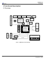
ADM-XRC-7V1 User Manual Revision: V1.5 ADM-XRC-7V1 User Manual © 2014 Copyright Alpha Data Parallel Systems Ltd. All rights reserved. This publication is protected by Copyright Law, with all rights reserved. No part of this publication may be reproduced, in any shape or form, without prior written consent from Alpha Data Parallel Systems Ltd. Address: Telephone: Fax: email: website: Head Office US Office 4 West Silvermills Lane, Edinburgh, EH3 5BD, UK +44 131 558 2600 +44 131 558 2700 [email protected] http://www.alpha-data.com 3507 Ringsby Court Suite 105, Denver, CO 80216 (303) 954 8768 (866) 820 9956 toll free [email protected] http://www.alpha-data.com All trademarks are the property of their respective owners. ADM-XRC-7V1 User Manual Table Of Contents 1 Introduction ...................................................................................................................................... 1 1.1 Key Features ................................................................................................................................. 1 1.2 References & Specifications .......................................................................................................... 1 2 Installation ........................................................................................................................................ 2 2.1 Software Installation ...................................................................................................................... 2 2.2 Hardware Installation ..................................................................................................................... 2 2.2.1 Handling Instructions ................................................................................................................. 2 2.2.2 Motherboard / Carrier Requirements ......................................................................................... 2 2.2.2.1 Installation in ADC-EMC-II Carrier ........................................................................................ 2 2.2.3 Cooling Requirements ............................................................................................................... 2 3 Functional Description .................................................................................................................... 4 3.1 Overview ........................................................................................................................................ 4 3.1.1 Switch Definitions ...................................................................................................................... 5 3.1.2 LED Definitions .......................................................................................................................... 6 3.2 XMC Platform Interface ................................................................................................................. 7 3.2.1 IPMI I2C ..................................................................................................................................... 7 3.2.2 MBIST# ...................................................................................................................................... 7 3.2.3 MVMRO ..................................................................................................................................... 7 3.2.4 MRSTI# ...................................................................................................................................... 7 3.2.5 MRSTO# .................................................................................................................................... 7 3.2.6 MPRESENT# ............................................................................................................................. 7 3.3 JTAG Interface ............................................................................................................................... 8 3.3.1 On-board Interface ..................................................................................................................... 8 3.3.2 XMC Interface ............................................................................................................................ 8 3.3.3 JTAG Voltages ........................................................................................................................... 8 3.4 Clocks ............................................................................................................................................ 9 3.4.1 200MHz Reference Clock (REFCLK200M) ............................................................................. 10 3.4.2 PCIe Reference Clock 0 (PCIEREFCLK0) .............................................................................. 10 3.4.3 PCIe Reference Clock 1 (PCIEREFCLK1) .............................................................................. 10 3.4.4 Programmable Clocks (LCLK, PROGCLK 0-3) ........................................................................ 11 3.4.5 Module-Carrier Global Clock (GCLK_M2C) ............................................................................. 11 3.4.6 Module-Carrier MGT Clock (MGTCLK_M2C) .......................................................................... 11 3.4.7 XRM LVDS Clock (XRM_LVDS_CLK) ..................................................................................... 11 3.5 Flash Memory .............................................................................................................................. 13 3.6 Configuration ............................................................................................................................... 14 3.6.1 Power-Up Sequence ................................................................................................................ 14 3.6.2 Bridge-Less Mode .................................................................................................................... 14 3.7 Health Monitoring ......................................................................................................................... 15 3.7.1 Automatic Temperature Monitoring .......................................................................................... 16 3.7.2 Microcontroller Status LEDs .................................................................................................... 16 3.8 Local Bus ..................................................................................................................................... 17 3.9 Target FPGA ................................................................................................................................ 17 3.9.1 I/O Bank Voltages .................................................................................................................... 17 3.9.2 Target MGT Links .................................................................................................................... 17 3.10 Memory Interfaces ....................................................................................................................... 19 3.11 XRM Interface and Front-Panel I/O ............................................................................................. 20 3.11.1 XRM Connector, CN1 .............................................................................................................. 20 3.11.2 XRM Connector CN2 ............................................................................................................... 20 3.11.3 XRM I/F - GPIO ....................................................................................................................... 20 3.11.4 XRM I/F - High-speed Serial Links .......................................................................................... 21 ADM-XRC-7V1 User Manual Appendix A Rear Connector Pinouts ............................................................................................................... 23 A.1 Primary XMC Connector, P5 ........................................................................................................ 23 A.2 Secondary XMC Connector, P6 ................................................................................................... 24 A.1 Pn6 GPIO Pin Map ...................................................................................................................... 25 A.3 PMC Connector P4 ...................................................................................................................... 27 A.4 Rear MGT Connections to the Target FPGA ............................................................................... 29 Appendix B Front (XRM) Connector Pinouts ................................................................................................... 31 B.1 XRM Connector CN1, Field 1 ...................................................................................................... 32 B.2 XRM Connector CN1, Field 2 ...................................................................................................... 33 B.3 XRM Connector CN1, Field 3 ...................................................................................................... 34 B.4 XRM Connector CN2 ................................................................................................................... 35 List of Tables Table 1 Table 2 Table 3 Table 4 Table 5 Table 6 Table 7 Table 8 Table 9 Table 10 Table 11 Table 12 Table 13 Table 14 Table 15 Table 16 Table 17 Table 18 Table 19 Table 20 Table 21 Table 22 Table 23 Table 24 Table 25 References ........................................................................................................................................ 1 Switch Definitions .............................................................................................................................. 5 LED Definitions .................................................................................................................................. 6 REFCLK200M Connections ............................................................................................................. 10 PCIEREFCLK Connections ............................................................................................................. 10 PROGCLK Connections .................................................................................................................. 11 GCLK_M2C Connections ................................................................................................................. 11 MGTCLK_M2C Connections ........................................................................................................... 11 XRM_LVDS_CLK Connections ........................................................................................................ 12 Voltage and Temperature Monitors .................................................................................................. 15 Temperature Limits .......................................................................................................................... 16 Status LED Definitions ..................................................................................................................... 16 Target FPGA IO Banks .................................................................................................................... 17 Target MGT Links ............................................................................................................................ 17 Maximum Memory Speeds .............................................................................................................. 19 XRM GPIO Groups .......................................................................................................................... 20 Pn5 Interface ................................................................................................................................... 23 Pn6 Interface ................................................................................................................................... 24 Pn6 GPIO Pin Map .......................................................................................................................... 25 Pn4 Interface ................................................................................................................................... 27 Target RearMGT Mapping ............................................................................................................... 29 XRM Connector CN1, Field 1 .......................................................................................................... 32 XRM Connector CN1, Field 2 .......................................................................................................... 33 XRM Connector CN1, Field 3 .......................................................................................................... 34 XRM Connector CN2 ....................................................................................................................... 35 Figure 1 Figure 2 Figure 3 Figure 4 Figure 5 Figure 6 Figure 7 Figure 8 ADM-XRC-7V1 Block Diagram .......................................................................................................... 4 LED Locations ................................................................................................................................... 6 JTAG Header J2 ................................................................................................................................ 8 JTAG Boundary Scan Chain .............................................................................................................. 8 Clocks ................................................................................................................................................ 9 Flash Memory Map .......................................................................................................................... 13 MGT Links ....................................................................................................................................... 18 DRAM Banks ................................................................................................................................... 19 List of Figures ADM-XRC-7V1 User Manual ADM-XRC-7V1 User Manual Page Intentionally left blank ADM-XRC-7V1 User Manual 1 Introduction The ADM-XRC-7V1 is a high-performance XMC for applications using Virtex-7 and Virtex-6 FPGAs from Xilinx. This card supports all Virtex-7 devices available in the FF(G), FH(G), and FL(G), 1761 package. The ADM-XRC-7V1 includes separate FPGA with a PCIe bridge developed by Alpha Data. Using a separate device allows high performance operation without the need to integrate proprietary cores in the user (target) FPGA. With the release of 7series FPGA boards, Alpha Data has introduced a new build option to allow the mezzanine card to be assembled without the bridge to reduce power and cost. The ADM-XRC-7V1 is available in air-cooled and conduction-cooled configurations. View the ADM-XRC-7V1 Ordering Info tab at ADM-XRC-7V1 Product Page on www.alpha-data.com. 1.1 Key Features Key Features • Single-width XMC, compliant to VITA Standard 42.0 and 42.3 • Dedicated 4-lane PCI-Express Gen 2 interface with high-performance DMA controllers • 4 additional PCI-Express compliant GTX links between user FPGA and P5 • Support for Virtex-7 FPGA in FF(G), FH(G), and FLG(G)1761 package • 4 independent banks of DDR3-1600 SDRAM, 256MB/bank, 1GB total (2GB and 4GB option) • Front-panel (XRM) interface with adjustable voltage, 146 GPIO signals and 8 GTX links to user FPGA • Rear-panel (XMC) 10 GTX links & 38 GPIO signals between user FPGA and P6 • Rear-panel (PMC) interface with 64 GPIO single ended or differential signals between user FPGA and P4 (optional) • Rear-Panel I/O (Pn6 and Pn4) compatible with 3U and 6U VPX carriers featuring various VITA 46.9 PMC/XMC to VPX signal mapping configurations • On-board programmable clocks enabling multiple protocols to be implemented on the user FPGA's high-speed links • Voltage and temperature monitoring • Air-cooled and conduction-cooled configurations 1.2 References & Specifications ANSI/VITA 42.0 XMC Standard, December 2008, VITA, ISBN 1-885731-49-3 ANSI/VITA 42.3 XMC PCI Express Protocol Layer Standard, June 2006, VITA, ISBN 1-885731-43-4 ANSI/VITA 46.9 PMC/MXC Rear I/O Fabric Signal Mapping on 3U and 6U VPX Modules Standard, November 2010, VITA, ISBN 1-885731-63-9 ANSI/IEEE 1386-2001 IEEE Standard for a Common Mezzanine Card (CMC) Family, October 2001, IEEE, ISBN 0-7381-2829-5 ANSI/IEEE 1386.1-2001 IEEE Standard Physical and Environmental Layers for PCI Mezzanine Cards (PMC), October 2001, IEEE, ISBN 0-7381-2831-7 ANSI/VITA 20-2001 (R2005) Conduction Cooled PMC, February 2005, VITA, ISBN 1-885731-26-4 Table 1 : References Introduction ad-ug-1248_v1_5.pdf Page 1 ADM-XRC-7V1 User Manual 2 Installation 2.1 Software Installation Please refer to the Software Development Kit (SDK) installation CD. The SDK contains drivers, examples for host control and FPGA design and comprehensive help on application interfacing. 2.2 Hardware Installation 2.2.1 Handling Instructions The components on this board can be damaged by electrostatic discharge (ESD). To prevent damage, observe SSD precautions: - Always wear a wrist-strap when handling the card - Hold the board by the edges - Avoid touching any components - Store in ESD safe bag. 2.2.2 Motherboard / Carrier Requirements The ADM-XRC-7V1 is a single width XMC.3 mezzanine with optional P6 and P4 connectors. The motherboard/ carrier must comply with the XMC.3 (VITA 42.3) specification for the Primary XMC connector, J5. The Secondary XMC connector, P6 has a pinout compatible with various XMC to VPX signal maps as defined by VITA 46.9. Please consult the pinouts in this user-guide as-well as those of the carrier manufacturer prior to installation. Assistance can be provided by Alpa Data. IMPORTANT Connector P6 on the card is not compatible with the VITA 42.10 (XMC GPIO) Standard. In particular, USB VCC must not be applied on this connector. The ADM-XRC-7V1 is compatible with either 5V or 12V on the "VPWR" power rail. 2.2.2.1 Installation in ADC-EMC-II Carrier The Alpha Data ADC-EMC-II carrier accepts both PMC and XMC mezzanine cards. By default, the carrier is configured for PMCs and connects all the serial links from the XMC connector J15 to J25. To configure for XMC and enable the PCIe interfaces at J15 and J25, switches 1-3 and 1-4 must be ON (closed). 2.2.3 Cooling Requirements The power dissipation of the board is highly dependent on the Target FPGA application. A power estimator spreadsheet is available on request from Alpha Data. This should be used in conjunction with Xilinx power estimation tools to determine the exact current requirements for each power rail. The board is supplied with a passive air cooled or conduction cooled heatsink according to the order number given at time of purchase. It is the users responsibility to ensure sufficient airflow for air cooled applications and metalwork for conduction cooled applications. Page 2 Installation ad-ug-1248_v1_5.pdf ADM-XRC-7V1 User Manual For more details on heatsinks supplied with Alpha Data boards, please view AD-AN-0018 ADM-XRC Cooling Solutions. The board features system monitoring that measures the board and FPGA temperature. It also includes a self-protection mechanism that will clear the target FPGA configuration if an over-temperature condition is detected. See Section 3.7 for further details. Installation ad-ug-1248_v1_5.pdf Page 3 ADM-XRC-7V1 User Manual 3 Functional Description 3.1 Overview Power Conversion P5 Mux IPMI EEPROM Configuration Switches Programmable Clocking Bridge x4 JTAG System Monitor FLASH XC6VLX130T (FF484) x4 SPI FLASH Mux x4 XRM2 DDR3 Bank1 39 DDR3 Bank2 37 DDR3 Bank3 35 DDR3 Bank3 19 (FFG/FLG/FHG 1761) 38 36 34 18 117 118 0 14 Target XC7V585T XC7V1500T XC7V2000T XC7VX330T XC7VX485T XC7VX690T 119 116 115 17 180-Way 16 15 114 XRM2 x8 113 33 28-Way 13 (HR) x2 x4 P4 P6 x4 Unused FPGA Banks GPIO Level Converter Quick Switch HR banks in X330T and 585T 64 GPIO 12 (HR) 31 32 111 112 Not in X330T and X485T Figure 1 : ADM-XRC-7V1 Block Diagram Page 4 Functional Description ad-ug-1248_v1_5.pdf ADM-XRC-7V1 User Manual 3.1.1 Switch Definitions There is a set of eight DIP switches placed on the rear of the board. Their functions are described in Switch Definitions. Note: All switches are OFF by default. Factory Configuration switch must be in the OFF position for normal operation. Switch Ref. Function ON State Off State SW1-1 User Switch to Target FPGA 0 1 SW1-2 Reserved - Normal Operation SW1-3 Bridge Bypass Bridge FPGA is bypassed - PCIe lanes Bridge FPGA is used. PCIe lanes (3:0) (3:0) are connected directly to the user are connected to the bridge. FPGA. SW1-4 Flash Boot Inhibit Target FPGA is not configured from onboard flash memory. Target FPGA is configured from onboard flash memory. SW1-5 XMC JTAG Connect JTAG chain to P5 Isolate JTAG chain from P5 SW1-6 E-Fuse Enable E-Fuse programming voltage (VccEFuse = 2.5V) Disable E-Fuse programming voltage (VccEFuse = 0V) SW1-7 Factory Configuration - Normal Operation SW1-8 Bridge-Less Mode Bridge-Less Mode Active - User bitstream loaded from SPI flash PCIe Bridge Mode Active - User bitstream loaded from Bridge Table 2 : Switch Definitions Functional Description ad-ug-1248_v1_5.pdf Page 5 ADM-XRC-7V1 User Manual 3.1.2 LED Definitions D14 XMC JTAG D13 NVMRO The position and description of the board status LEDs are shown in LED Locations: D7 Status 1 D8 Status 2 D9 Target Done D10 Bridge Done D11 Bridge-Bypass D12 Bridge-Less Figure 2 : LED Locations Comp. Ref. Function ON State D7(Red) Status 1 See Status LED Definitions D8(Green) Status 2 See Status LED Definitions Off State D9(Green) Target Done Target FPGA is configured Target FPGA is unconfigured D10(Green) Bridge Done Bridge FPGA is configured Bridge FPGA is unconfigured D11(Amber) Bridge Bypass Bridge FPGA is bypassed - PCIe lanes Bridge FPGA is used. PCIe lanes (3:0) (3:0) are connected directly to the user are connected to the bridge. FPGA D12(Amber) Bridge-Less Target is configured through Auxiliary SPI memmory Target is configured by Bridge D13(Amber) NVMRO Inhibit writes to non-volatile memories Enable writes to non-volatile memories D14(Amber) XMC JTAG On-board JTAG chain connected to P5 On-board JTAG chain is isolated from P5 Table 3 : LED Definitions Page 6 Functional Description ad-ug-1248_v1_5.pdf ADM-XRC-7V1 User Manual 3.2 XMC Platform Interface 3.2.1 IPMI I2C A 4 Kbit I2C EEPROM (type M24C04) is connected to the XMC IPMI. This memory contains board information (type, voltage requirements etc.) as defined in the XMC based specification. 3.2.2 MBIST# Built-In Self Test. This output signal is driven active (low) until the FPGA with PCIe interface is configured. In normal operation, this is the bridge FPGA. In Bridge Bypass mode or Bridge-Less Mode, it is the target FPGA. 3.2.3 MVMRO XMC Write Prohibit. This signal is an input from the carrier. When asserted (high), all writes to non-volatile memories are inhibited. This is indicated by the Amber LED, D7. This signal cannot be internally driven or over-ridden. A buffered version of the signal is connected to the target FPGA at pin AG32. 3.2.4 MRSTI# XMC Reset In. This signal is an active low input from the carrier. When asserted, the bridge FPGA will be reset. The MRSTI# signal is translated to 1.8V levels and connected to the target FPGA at pin AF30. 3.2.5 MRSTO# XMC Reset Out. This optional output signal is unused and undriven. 3.2.6 MPRESENT# Module Present. This output signal is connected directly to 0V. Functional Description ad-ug-1248_v1_5.pdf Page 7 ADM-XRC-7V1 User Manual 3.3 JTAG Interface 3.3.1 On-board Interface A JTAG boundary scan chain is connected to header J3. This allows the connection of the Xilinx JTAG cable for FPGA debug using the Xilinx ChipScope tools. The JTAG Header pinout is shown in JTAG Header J2: TDI TMS TCK TDO VCC GND Figure 3 : JTAG Header J2 The scan chain is shown in JTAG Boundary Scan Chain: Header J3 XMC Con (Pn5) XMC_TDI XMC_TDO VREF (1.8V) HDR_TDI Level Shift 3.3V – 1.8V Bridge FPGA XC6VLX130T FFG484 Control CPLD XC2C64A CP56 Target FPGA XC7VxxxxT FFG1759 HDR_TDO En# XRM_TDI Level Shift 1.8V - XRM_VIO En# XMC_JTAG_EN# SW1E XRM_TDO XRM I/F PRESENT# Figure 4 : JTAG Boundary Scan Chain If the boundary scan chain is connected to the interface at the XMC connector (SW1-5 is ON), Header J3 should not be used. 3.3.2 XMC Interface The JTAG interface on the XMC connector is normally unused and XMC_TDI connected directly to XMC_TDO. The interface can be connected to the on-board interface (through level-translators) by switching SW1-5 ON. See Switch Definitions 3.3.3 JTAG Voltages The on-board JTAG scan chain uses 1.8V. The Vcc supply provided on J2 to the JTAG cable is +1.8V and is protected by a poly fuse rated at 350mA. 3.3V signals must not be used at header J2. The JTAG signals at the XMC interface use 3.3V signals and are connected through level translators to the on-board scan chain. The JTAG signals at the XRM interface use the adjustable voltage XRM_VIO. Page 8 Functional Description ad-ug-1248_v1_5.pdf ADM-XRC-7V1 User Manual 3.4 Clocks The ADM-XRC-7V1 provides a wide variety of clocking options. On top of a fixed 200MHz oscillator and clocks routed from the rear and front panel connectors, the board has 4 user-programmable clocks. These clocks can be combined with the FPGA's internal PLLs to suit a wide variety of communication protocols. A complete overview of the clock routing on the ADM-XRC-7V1 is given in Clocks. A description of each clock follows. 7 Series MGT/ Banks Bank 14 DDR3 Banks 19 35 37 39 250MHZ Source REFCLK0 MGT119 REFCLK1 200MHZ Source 200MHZ Buffer REFCLK0 MGT118 REFCLK1 REFCLK0 MGT117 PCIe Bridge REFCLK1 REFCLK0 XMC P5 MGT116 PCIe REFCLK Buffer REFCLK1 REFCLK0 MGT115 REFCLK1 REFCLK0 MGT114 XMC P6 REFCLK1 REFCLK0 MGT113 REFCLK1 REFCLK0 MGT112 User Programmable Source REFCLK1 REFCLK0 MGT111 REFCLK Buffer Note: REFCLK can be shared with MGT tiles to the North and South within a super logic region (SLR in 1500T and 2000T only) REFCLK1 XRM Interface Figure 5 : Clocks Note: Clock Termination The LVDS clocks do not have termination resistors on the circuit board. On-die terminations in the FPGA must be enabled by setting the attribute "DIFF_TERM = TRUE". This can either be set in the source code when instantiating the buffer, or in the User Constraints File (UCF). See the Xilinx Virtex-7 Libraries Guide and Constraints Guide for further details. Functional Description ad-ug-1248_v1_5.pdf Page 9 ADM-XRC-7V1 User Manual 3.4.1 200MHz Reference Clock (REFCLK200M) The fixed 200MHz reference clock REFCLK200M is a differential clock signal using LVDS. This signal is widely distributed throughout the board. It is connected to a MRCC inputs on the Target FPGA on Bank 14. REFCLK200M is also converted to HSTL signaling and used as the input clock for the DRAM interface. This clock can be used to generate application-specific clock frequencies using the PLLs within the Virtex-7 FPGA. It is also suitable as the reference clock for the IO delay control block (IDELAYCTRL). Signal Frequency Target FPGA Input REFCLK200M "P" pin "N" pin IO_L12_T2_MRCC_14 LVDS AK34 AL34 REFCLK200M_HSTL 200 MHz 200 MHz IO_L12_T1_MRCC_19 HSTL_I IO Standard L39 L40 REFCLK200M_HSTL 200 MHz IO_L12_T1_MRCC_35 HSTL_I E34 E35 REFCLK200M_HSTL 200 MHz IO_L12_T1_MRCC_37 HSTL_I D27 D28 REFCLK200M_HSTL 200 MHz IO_L12_T1_MRCC_39 HSTL_I H15 H14 REFCLK200M 200 MHz MGTREFCLK0_115 LVDS Y8 Y7 REFCLK200M 200 MHz MGTREFCLK0_118 LVDS G10 G9 Table 4 : REFCLK200M Connections 3.4.2 PCIe Reference Clock 0 (PCIEREFCLK0) The 100MHz PCI Express reference clock is provided by the carrier card through the Primary XMC connector, P5 at pins A19 and B19. This clock is buffered into two PLE Express reference clocks that are forwarded to the Bridge and User FPGA respectively. Signal Frequency Target FPGA Input IO Standard "P" pin "N" pin PCIEREFCLK 100 MHz MGTREFCLK0_117 LVDS K8 K7 Table 5 : PCIEREFCLK Connections 3.4.3 PCIe Reference Clock 1 (PCIEREFCLK1) The reference clock "PCIEREFCLK1" is a differential clock provided by a carrier card through the Secondary XMC connector P6 at pins A19 and B19. The Default build configuration for this board connects this pair to the MGT signal inputs. Most needed reference clocks can be generated through the User Programmable clocking options. If it is a requirement that this differential pair be utilized as a clock signal to an MGT bank, a resistor fit option is available. Please contact Alpha Data for detials. Page 10 Functional Description ad-ug-1248_v1_5.pdf ADM-XRC-7V1 User Manual 3.4.4 Programmable Clocks (LCLK, PROGCLK 0-3) There are two programable clock sources that are forwarded throughout the FPGA. These clocks are programmable through the Alpha Data ADM-XRC Gen 3 SDK. LCLK is generated in the Bridge FPGA by the the Alpha Data ADB3 driver and offers a less accurate frequency resolution, but with a wider programmable frequency range. PROGCLK[3:0] is generated by a dedicated programmable clock generator IC and offer extremely high frequency resolutions (1ppm increments). PROGCLK[3:0] is generated by a single source and buffered to all MGT tiles. Signal Frequency Target FPGA Input IO Standard "P" pin "N" pin LCLK 5 - 700 MHz IO_L13_MRCC_14 LVDS AJ32 AK32 PROGCLK0 5 - 312.5 MHz MGTREFCLK1_113 LVDS AK8 AK7 PROGCLK1 5 - 312.5 MHz MGTREFCLK1_115 LVDS AB8 AB7 PROGCLK2 5 - 312.5 MHz MGTREFCLK1_117 LVDS M8 M7 PROGCLK3 5 - 312.5 MHz MGTREFCLK1_119 LVDS C10 C9 Table 6 : PROGCLK Connections 3.4.5 Module-Carrier Global Clock (GCLK_M2C) The clock "GCLK_M2C" is a differential clock signal using LVDS. It is provided by an XRM module through the XRM connector, CN1, at pins 110 & 108. It is connected to an MRCC input on the Target FPGA. Signal Frequency GCLK_M2C Variable Target FPGA Input IO Standard IO_L13_T2_MRCC_17 LVDS "P" pin "N" pin AF39 AF40 Table 7 : GCLK_M2C Connections 3.4.6 Module-Carrier MGT Clock (MGTCLK_M2C) The reference clock "MGTCLK_M2C" is a differential clock signal using LVDS. The clock is provided by an XRM module through the XRM connector, CN1, at pins 109 & 111. It is first buffered and fanned out, then connected to GTX Quads 113 and 114 on the Target FPGA for application specific frequencies / line rates. Signal Frequency Target FPGA Input IO Standard "P" pin "N" pin MGTCLK_M2C Variable MGTREFCLK0_113 LVDS AH8 AH7 MGTCLK_M2C Variable MGTREFCLK0_114 LVDS AD8 AD7 Table 8 : MGTCLK_M2C Connections 3.4.7 XRM LVDS Clock (XRM_LVDS_CLK) The clock "XRM_LVDS_CLK" is a differential clock signal using LVDS levels. The clock is provided by the target FPGA and connected to an XRM module through the XRM connector, CN1, at pins 113 & 115. Functional Description ad-ug-1248_v1_5.pdf Page 11 ADM-XRC-7V1 User Manual Signal Frequency Target FPGA Input XRM_PECL_CLK Variable IO_L13_T2_MRCC_15 LVDS IO Standard "P" pin "N" pin AV40 AW40 Table 9 : XRM_LVDS_CLK Connections Page 12 Functional Description ad-ug-1248_v1_5.pdf ADM-XRC-7V1 User Manual 3.5 Flash Memory A 512Mb Flash Memory (Intel / Numonyx PC28F512P30EF) is used to store board Vital Product Data (VPD), programmable clock parameters and configuration bitstreams for the Bridge and Target FPGAs. The flash memory cannot be accessed by the target FPGA. Host access is only possible through the FLCTL, FLPAGE and FLDATA registers in the Bridge FPGA. The region of memory between addresses 0x11000000 and 0x11FFFFF is allocated for custom data to be stored by the ADM-XRC-7V1 user. Utilities for erasing, programming and verification of the flash memory are provided in the ADMXRC SDK. Write Protect The Flash Write Protect (WP#) pin is connected to an inverted version of the NVMRO signal at the XMC interface. When the NVMRO signal is active (High), all writes to the flash will be inhibited. This state will be indicated by the Amber LED as shown in LED Locations. Alternate Bridge FPGA Bitstream 0x0000_0000 0x007F_FFFF 0x0080_0000 Default Bridge FPGA Bitstream Alpha Data Vital Product Data (Alpha Data VPD) 0x00FF_FFFF 0x0100_0000 0x010F_FFFF 0x0110_0000 User Vital Product Data (User VPD) B0 Length(7:0) Boot Flag 0 Bitstream 0 Length(23:8) 0x011F_FFFF 0x0120_0000 0x0120_0002 reserved Default Target FPGA Bitstream (Target Bitstream 0) B1 Length(7:0) Boot Flag 1 Bitstream 1 Length(23:8) 0x0122_0000 0x028F_FFFF 0x0290_0000 0x0290_0002 reserved Alternate Target FPGA Bitstream (Target Bitstream 1) 0x0292_0000 0x03FF_FFFF Figure 6 : Flash Memory Map Functional Description ad-ug-1248_v1_5.pdf Page 13 ADM-XRC-7V1 User Manual 3.6 Configuration 3.6.1 Power-Up Sequence If valid data is stored in the flash memory, the bridge will automatically configure the Target FPGA at power-up. This sequence can be inhibited by turning the Flash Boot Inhibit (FBI) switch, SW1-4 to ON. (See Switch Definitions). Note: If an over-temperature alert is detected from the System Monitor, the target will be cleared by pulsing its PROG signal. See Automatic Temperature Monitoring. 3.6.2 Bridge-Less Mode When operating in bridgeless mode, the Target FPGA will be configured directly by a Quad SPI connection to a 1Gb FLASH memory device. This memory device is re-programable over a Xilinx JTAG cable. This mode is not available in Revision 2 and earlier boards. Page 14 Functional Description ad-ug-1248_v1_5.pdf ADM-XRC-7V1 User Manual 3.7 Health Monitoring The ADM-XRC-7V1 has the ability to monitor temperature and voltage to maintain a check on the operation of the board. The monitoring is implemented using the ATMEGA64 microcontroller. Control algorithms within the microcontroller automatically check line voltages and on board temperaturs and shares the information with blockram in the Bridge FPGA. The following voltage rails and temperatures are monitored: Monitor Purpose 1.0V FPGA Core Supply (VccINT) 1.0V Target Tranceiver Power (AVCC) 1.0V Bridge Tranceiver Power (AVCC) 1.2V Target Tranceiver Power (AVTT) 1.2V Bridge Tranceiver Power (AVTT) 1.5V DDR3 SDRAM, Target FPGA memory I/O XRM_VIO (Front-Panel) I/O voltage 1.8V Target Tranceiver Power (AVCC_AUX) 1.8V Flash Memory, FPGA IO Voltage (VCCO) 2.0V Target FPGA Auxiliary Supply AUX (VccAUX) 2.5V Level Translation, Bridge FPGA Auxiliary Supply (VccAUX) 3.3V Board Input Supply 5.0V Internally generated 5V supply VPWR Board Input Supply (either 5.0V or 12.0V) Temp1 Target FPGA on-die temperature Temp2 Board temperature sensor on-die temperature Temp3 Bridge FPGA on-die temperature Table 10 : Voltage and Temperature Monitors An example application that reads the system monitor ("sysmon") is available within the SDK. Functional Description ad-ug-1248_v1_5.pdf Page 15 ADM-XRC-7V1 User Manual 3.7.1 Automatic Temperature Monitoring At power-up, the control logic sets the temperature limits and resets the LM87's over-temperature interrupt. The temperature limits are shown in Table Temperature Limits: . Target FPGA Bridge FPGA Board Min Max Min Max Min Max Commercial 0 degC +85 degC 0 degC +85 degC 0 degC +85 degC Extended 0 degC +100 degC 0 degC +100 degC 0 degC +100 degC Industrial -40 degC +100 degC -40 degC +100 degC -40 degC +100 degC Table 11 : Temperature Limits Important: If any temperature limit is exceeded, the Target FPGA is automatically cleared. This is indicated by the Green LED (Target Configured) switching off and the two status LEDs showing a temperature fault indication. The purpose of this mechanism is to protect the card from damage due to over-temperature. It is possible that it will cause the user application and, possibly, the host computer to "hang". 3.7.2 Microcontroller Status LEDs LEDs D7 (Red) and D8 (Green) indicate the microcontroller status. LEDs Status Green Running and no alarms Green + Red Standby (Powered off) Flashing Green + Flashing Red (together) Attention - critical alarm active Flashing Green + Flashing Red (alternating) Service Mode Flashing Green + Red Attention - alarm active Red Missing application firmware or invalid firmware Flashing Red FPGA configuration cleared to protect board Table 12 : Status LED Definitions Page 16 Functional Description ad-ug-1248_v1_5.pdf ADM-XRC-7V1 User Manual 3.8 Local Bus A Multiplexed Packet Transport Link (MPTL) connects the Bridge and Target FPGAs. It is capable of transferring data at up to 2GB/s simultaneously in each direction. The MPTL replaces the parallel local bus used in previous generations of the ADM-XRC series. Details of the link and example designs are given in the Software Development Kit (SDK). 3.9 Target FPGA 3.9.1 I/O Bank Voltages The Target FPGA IO is arranged in banks, each with their own supply pins. The bank numbers, their voltage and function are shown in Target FPGA IO Banks. Full details of the IOSTANDARD required for each signal are given in the SDK. IO Banks Voltage Purpose 0, 14 1.8V Configuration, JTAG, LBus Control,XMC Control,Target SelectMap Interface 13, 33 1.8V Pn4 & Pn6 GPIO 15, 16, 17 XRM_VIO XRM Interface (variable voltage) 18, 19, 34, 35, 36, 37, 38, 39 1.5V DRAM Banks 0-3 Table 13 : Target FPGA IO Banks 3.9.2 Target MGT Links There are a total of 26 Multi-Gigabit Transceiver (MGT) links connected to the Target FPGA: Links Width Connection PCIe(3:0) 4 Bridge FPGA (for MPTL) or XMC Connector P5 lanes (3:0) in Bridge Bypass Mode PCIe(7:4) 4 Direct link to XMC P5 lanes (7:4) P6(9:0) 10 Direct link to XMC P6 lanes (9:0) FrontMGT(7:0) 8 Direct link to XRM interface Table 14 : Target MGT Links The connections of these links are shown in MGT Links: For MGT Clocking see Clocks: Functional Description ad-ug-1248_v1_5.pdf Page 17 ADM-XRC-7V1 User Manual 7 Series MGT/ Banks RearMGT(16:17) MGT119 PCIe Bridge RearMGT(3:0) MGT118 MGT117 Bridge Bypass MGT116 XMC P5 RearMGT(7:4) MGT115 RearMGT(8:11) XMC P6 MGT114 RearMGT(12:15) RearMGT(16:17) MGT113 MGT112 MGT111 XRM(3:0) XRM(7:4) XRM Interface Figure 7 : MGT Links Page 18 Functional Description ad-ug-1248_v1_5.pdf ADM-XRC-7V1 User Manual 3.10 Memory Interfaces The ADM-XRC-7V1 has four independent banks of DDR3 SDRAM. Each bank consists of two 16 bit wide memory devices in parallel to provide a 32 bit datapath capable of running up to 800MHz (DDR-1600). 2Gb devices (Micron MT41J64M16-187E) are fitted as standard to provide 512MB per bank. 4Gb (giving 1GB per bank) are available as an ordering option. The memory banks are arranged for compatibility with the Xilinx Memory Interface Generator (MIG). DRAM Banks Shows the component references and FPGA banks used. Full details of the interface, signaling standards and an example design are provided in the SDK. DRAM Bank 3 DRAM Bank 2 Bank 39 Bank 37 Bank 38 200MHz REFCLK Bank 36 Virtex 7 Bank 35 Bank 34 DRAM Bank 1 Bank 19 Bank 18 DRAM Bank 0 Figure 8 : DRAM Banks FPGA Speed Grade Single Rank (2GB-4GB) Dual Rank (8GB) -3 1600 1333 -2/-2L/-2G 1600 1333 -1 1600 1066 1066 Contact Support -1M Table 15 : Maximum Memory Speeds Functional Description ad-ug-1248_v1_5.pdf Page 19 ADM-XRC-7V1 User Manual 3.11 XRM Interface and Front-Panel I/O The XRM interface provides a high-performance and flexible front-panel interface through a range of interchangeable XRM modules. Further details of the XRM modules can be found on the Alpha Data website. The XRM interface consists of two samtec connectors, CN1 and CN2. 3.11.1 XRM Connector, CN1 Connector CN1 is for general-purpose signals, power and module control. The connector is a 180-way Samtec connector with 3 fields. The part fitted to the ADM-XRC-7V1 is Samtec QSH-090-01-F-D-A-K. Full pinout information for this connector is listed in XRM Connector CN1, Field 1 to XRM Connector CN1, Field 3. 3.11.2 XRM Connector CN2 Connector CN2 is for the high-speed serial (MGT) links. The part fitted to the ADM-XRC-7V1 is Samtec QSE-014-01-F-D-DP-A-K. Full pinout information for this connector is listed in XRM Connector CN2. 3.11.3 XRM I/F - GPIO The general purpose IO (GPIO) signals are connected in 4 groups to the Target FPGA. Each group consists of 16 standard I/O pairs, a Regional Clock Capable pair and either 2 or 4 single-ended signals. There are no on-board terminations on the pairs and any can be used in single-ended modes. To allow fast data transfer, all of the GPIO signals within a group are delay matched to within 100ps. All the XRM GPIO signals and FPGA IO banks share a common voltage, XRM_VIO, that can be either 1.8V, 1.5V or 1.2V. The required voltage is stored within the platform management PROM on the XRM. Group FPGA Bank Group A 16-17 Group B Group C Group D 15-16 15 17 Name Function XRM_DA (15:0) 16 diff. Pairs / 32 single-ended XRM_DA_CC (16) Regional Clock / GPIO pair / 2 single-ended SA (1:0) 2 single-ended GPIO XRM_DB (15:0) 16 diff. Pairs / 32 single-ended XRM_DB_CC (16) Regional Clock / GPIO pair / 2 single-ended SB (1:0) 2 single-ended GPIO XRM_DC (15:0) 16 diff. Pairs / 32 single-ended XRM_DC_CC (16) Regional Clock / GPIO pair / 2 single-ended SC (1:0) 2 single-ended GPIO XRM_DD (15:0) 16 diff. Pairs / 32 single-ended XRM_DD_CC (16) Regional Clock / GPIO pair / 2 single-ended Table 16 : XRM GPIO Groups (continued on next page) Page 20 Functional Description ad-ug-1248_v1_5.pdf ADM-XRC-7V1 User Manual Group FPGA Bank Name Function Group D 17 SD (3:0) 4 single-ended GPIO Table 16 : XRM GPIO Groups 3.11.4 XRM I/F - High-speed Serial Links Eight MGT links are routed between the Target FPGA and the XRM interface. Lanes (6:0) are routed through the Samtec QSE-DP connector, CN2. Lane (7) is routed through the Samtec QSH connector, CN1. Functional Description ad-ug-1248_v1_5.pdf Page 21 ADM-XRC-7V1 User Manual Page Intentionally left blank Page 22 Functional Description ad-ug-1248_v1_5.pdf ADM-XRC-7V1 User Manual Appendix A: Rear Connector Pinouts Appendix A.1: Primary XMC Connector, P5 . A B C D E 1: PET_PO PET_NO 3V3 PET_P1 PET_N1 VPWR 2: GND GND TRST_L GND GND MRSTI_L F 3: PET_P2 PET_P3 PET_N2 3V3 PET_N3 VPWR 4: GND GND TCK GND GND MRSTO_L 5: PET_P4 PET_N4 3V3 PET_P5 PET_N5 VPWR 6: GND GND TMS GND GND 7: PET_P6 PET_N6 3V3 PET_P7 PET_N7 VPWR 8: GND GND TDI GND GND M12V0 - VPWR 9: - - - - 12V0 10: GND GND TDO GND GND GAO 11: PER_PO PER_NO MBIST_L PER_P1 PER_N1 VPWR MPRESENT_L 12: GND GND GA1 GND GND 13: PER_P2 PER_N2 3V3_AUX PER_P3 PER_N3 VPWR 14: GND GND GA2 GND GND I2C_SDA 15: PER_P4 PER_N4 - PER_P5 PER_N5 VPWR 16: GND GND MVMRO GND GND MSCL 17: PER_P6 PER_N6 - PER_P7 PER_N7 - 18: GND GND - GND GND - 19: REFCLK0_P REFCLK0_N - WAKE_L ROOTO_L - Table 17 : Pn5 Interface Rear Connector Pinouts ad-ug-1248_v1_5.pdf Page 23 ADM-XRC-7V1 User Manual Appendix A.2: Secondary XMC Connector, P6 . A B C D E F 1: PN6_TX_P0 PN6_TX_N0 GP37 PN6_TX_P1 PN6_TX_N1 GP38 2: GND GND GP35 GND GND GP36 3: PN6_TX_P2 PN6_TX_N2 GP33 PN6_TX_P3 PN6_TX_N3 GP34 4: GND GND GP31 GND GND GP32 5: PN6_TX_P4 PN6_TX_N4 GP29 PN6_TX_P5 PN6_TX_N5 GP30 6: GND GND GP27 GND GND GP28 7: PN6_TX_P6 PN6_TX_N6 GP25 PN6_TX_P7 PN6_TX_N7 GP26 8: GND GND GP23 GND GND GP24 9: PN6_TX_P8 PN6_TX_N8 GP21 PN6_TX_P9 PN6_TX_N9 GP22 10: GND GND GP19 GND GND GP20 11: PN6_RX_P0 PN6_RX_N0 GP17 PN6_RX_P1 PN6_RX_N1 GP18 12: GND GND GP15 GND GND GP16 13: PN6_RX_P2 PN6_RX_N2 GP13 PN6_RX_P3 PN6_RX_N3 GP14 14: GND GND GP11 GND GND GP12 15: PN6_RX_P4 PN6_RX_N4 GP9 PN6_RX_P5 PN6_RX_N5 GP10 16: GND GND GP7 GND GND GP8 17: PN6_RX_P6 PN6_RX_N6 GP5 PN6_RX_P7 PN6_RX_N7 GP6 18: GND GND GP3 GND GND GP4 19: PN6_RX_P8 PN6_RX_N8 GP1 PN6_RX_P9 PN6_RX_N9 GP2 Table 18 : Pn6 Interface Page 24 Rear Connector Pinouts ad-ug-1248_v1_5.pdf ADM-XRC-7V1 User Manual Appendix A.1: Pn6 GPIO Pin Map Signal FPGA Pin FPGA Bank GP1 BA32 13 GP2 BA30 13 GP3 BA31 13 GP4 BB31 13 GP5 AW31 13 GP6 AY32 13 GP7 AV30 13 GP8 AY30 13 GP9 AV35 13 GP10 AR35 13 GP11 AW33 13 GP12 AV33 13 GP13 AV34 13 GP14 AY33 13 GP15 AT35 13 GP16 AW30 13 GP17 AW32 13 GP18 AV31 13 GP19 AT31 13 GP20 AU32 13 GP21 AR30 13 GP22 AU31 13 GP23 AT32 13 GP24 AN20 33 GP25 AL24 33 GP26 AR33 13 GP27 AU33 13 GP28 AT30 13 GP29 AP32 13 GP30 AP31 13 GP31 AR34 13 GP32 AR32 13 GP33 AP30 13 GP34 AP33 13 Table 19 : Pn6 GPIO Pin Map (continued on next page) Rear Connector Pinouts ad-ug-1248_v1_5.pdf Page 25 ADM-XRC-7V1 User Manual Signal FPGA Pin FPGA Bank GP35 AN30 13 GP36 AL32 14 GP37 AL31 14 GP38 AN31 13 Table 19 : Pn6 GPIO Pin Map GCC: Global clock capable Page 26 MRCC: Multi-region clock capable SRCC: Single-region clock capable Rear Connector Pinouts ad-ug-1248_v1_5.pdf ADM-XRC-7V1 User Manual Appendix A.3: PMC Connector P4 Signal FPGA Pin Clock Capability P4 Pin P4 Pin Clock Capability FPGA Pin Signal PN4_P1 AK20 - 1 2 - AJ21 PN4_P2 AJ20 PN4_N2 PN4_N1 AL20 - 3 4 - PN4_P3 AJ23 - 5 6 - AJ22 PN4_P4 PN4_N3 AK23 - 7 8 - AK22 PN4_N4 PN4_P5 AM24 - 9 10 - AL21 PN4_P6 PN4_N5 AN24 - 11 12 - AM21 PN4_N6 PN4_P7 AL22 - 13 14 - AN21 PN4_N7 AM22 - 15 16 - AP21 PN4_N8 PN4_P9 AM23 - 17 18 - AP23 PN4_P10 PN4_N10 PN4_N9 PN4_P8 AN23 - 19 20 - AP22 PN4_P11 AT34* - 21 22 SRCC AR23 PN4_P12 PN4_N11 AU34* - 23 24 SRCC AR22 PN4_N12 PN4_P13 AU23 MRCC 25 26 MRCC AT22 PN4_P14 PN4_N13 AV23 MRCC 27 28 MRCC AU22 PN4_N14 PN4_P15 AY35* - 29 30 - AU24 PN4_P16 PN4_N15 AW35* - 31 32 - AV24 PN4_N16 PN4_P17 AT36* - 33 34 - AR24 PN4_P18 PN4_N17 AU36* - 35 36 - AT24 PN4_N18 PN4_P19 AT21 - 37 38 - AV36* PN4_P20 PN4_N19 AU21 - 39 40 - AW36* PN4_N20 PN4_P21 AY23 - 41 42 - AV21 PN4_P22 PN4_N21 AY22 - 43 44 - AW21 PN4_N22 PN4_P23 AY25 - 45 46 SRCC AW23 PN4_P24 PN4_N23 BA25 - 47 48 SRCC AW22 PN4_N24 PN4_P25 BA21 - 49 50 - AY24 PN4_P26 PN4_N25 BB21 - 51 52 - BA24 PN4_N26 PN4_P27 BB24 - 53 54 - BA22 PN4_P28 PN4_N27 BB23 - 55 56 - BB22 PN4_N28 PN4_P29 AY34* - 57 58 - BB32* PN4_P30 PN4_N29 BA35* - 59 60 - BB33* PN4_N30 PN4_P31 BA34* - 61 62 - BA36* PN4_P32 PN4_N31 BB34* - 63 64 - BB36* PN4_N32 Table 20 : Pn4 Interface MRCC: Multi-region clock capable Rear Connector Pinouts ad-ug-1248_v1_5.pdf SRCC: Single-region clock capable Page 27 ADM-XRC-7V1 User Manual * For XCV550T or XCV330T pins cannot be used as LVDS Page 28 Rear Connector Pinouts ad-ug-1248_v1_5.pdf ADM-XRC-7V1 User Manual Appendix A.4: Rear MGT Connections to the Target FPGA In normal mode, the target FPGA RearMGT lanes (3:0) are connected to the Bridge FPGA. In Bridge Bypass Mode, they are connected to P5 lanes (3:0). RearMGT Lanes (7:4) are connected directly to P5 lanes (7:4). RearMGT Lanes (17:8) are connected directly to P6 lanes (9:0). The pin mappings are as follows: Rear Connector + Pin Rear Connector - Pin RearMGT_TX_0 J2 J1 P5.A1 P5.B1 RearMGT_TX_1 Signal FPGA + Pin H4 FPGA - Pin H3 P5.D1 P5.E1 RearMGT_TX_2 G2 G1 P5.A3 P5.B3 RearMGT_TX_3 F4 F3 P5.D3 P5.E3 RearMGT_TX_4 K4 K3 P5.A5 P5.B5 RearMGT_TX_5 L2 L1 P5.D5 P5.E5 RearMGT_TX_6 M4 M3 P5.A7 P5.B7 RearMGT_TX_7 N2 N1 P5.D7 P5.E7 RearMGT_TX_8 P4 P3 P6.A1 P6.B1 RearMGT_TX_9 R2 R1 P6.D1 P6.E1 RearMGT_TX_10 T4 T3 P6.A3 P6.B3 RearMGT_TX_11 U2 U1 P6.D3 P6.E3 RearMGT_TX_12 W2 W1 P6.A5 P6.B5 RearMGT_TX_13 AA2 AA1 P6.D5 P6.E5 RearMGT_TX_14 AC2 AC1 P6.A7 P6.B7 RearMGT_TX_15 AE2 AE1 P6.D7 P6.E7 RearMGT_TX_16 D4 D3 P6.A9 P6.B9 RearMGT_TX_17 E2 E1 P6.D9 - - - - - RearMGT_RX_0 H8 H7 P5.A11 P5.B11 RearMGT_RX_1 G6 G5 P5.D11 P5.D11 P6.E9 RearMGT_RX_2 F8 F7 P5.A13 P5.B13 RearMGT_RX_3 E6 E5 P5.D13 P5.E13 RearMGT_RX_4 J6 J5 P5.A15 P5.B15 RearMGT_RX_5 L6 L5 P5.D15 P5.E15 RearMGT_RX_6 N6 N5 P5.A17 P5.B17 RearMGT_RX_7 P8 P7 P5.D17 P5.E17 RearMGT_RX_8 R6* R5* P6.A11 P6.B11 Table 21 : Target RearMGT Mapping (continued on next page) Rear Connector Pinouts ad-ug-1248_v1_5.pdf Page 29 ADM-XRC-7V1 User Manual Signal FPGA + Pin FPGA - Pin RearMGT_RX_9 U6 U5 P6.D11 P6.E11 RearMGT_RX_10 V4 V3 Rear Connector + Pin P6.A13 Rear Connector - Pin P6.B13 RearMGT_RX_11 W6 W5 P6.D13 P6.E13 RearMGT_RX_12 Y4 Y3 P6.A15 P6.B15 RearMGT_RX_13 AA6 AA5 P6.D15 P6.E15 RearMGT_RX_14 AB4 AB3 P6.A17 P6.B17 RearMGT_RX_15 AC6 AC5 P6.D17 P6.E17 RearMGT_RX_16 C6 C5 P6.A19 P6.B19 RearMGT_RX_17 D8 D7 P6.D19 P6.E19 Table 21 : Target RearMGT Mapping * This differential pair is connected with reverse polarity. Use the invert polarity bit of the GTX configuration to correct the polarity inversion. Page 30 Rear Connector Pinouts ad-ug-1248_v1_5.pdf ADM-XRC-7V1 User Manual Appendix B: Front (XRM) Connector Pinouts The XRM interface consists of two connectors: CN1 and CN2. CN1 is a 180-way Samtec QSH in 3 fields. It is for general-purpose signals, power and module control. CN2 is a 28-way Samtec QSE-DP for high-speed serial (MGT) links. Power JTAG & Platform Management General Purpose I/O Clocks MGT Links Front (XRM) Connector Pinouts ad-ug-1248_v1_5.pdf Page 31 ADM-XRC-7V1 User Manual Appendix B.1: XRM Connector CN1, Field 1 Signal FPGA Samtec Samtec FPGA Signal DA_N0 AE35 1 2 AD31 DA_N1 DA_P0 AE34 3 4 AC31 DA_P1 DA_N2 Y33 5 6 AB31 DA_P3 DA_P2 Y32 7 8 AB32 DA_N3 Y40 DA_N5 DA_N4 9 10 DA_P4 AE32 11 12 W40 DA_P5 DA_N6 AD35 AE33 13 14 AE30 DA_N7 DA_P6 AC34 15 16 AE29 DA_P7 DA_P8 AF31 17 18 Y42 DA_P9 DA_N8 AF32 19 20 AA42 DA_N9 DA_N10 AA32 21 22 AD30 DA_N11 AC30 DA_P10 AA31 23 24 DA_N12 AB42 25 26 Y39 DA_P13 DA_P12 AB41 27 28 AA39 DA_N13 DA_P11 DA_N14 AA30 29 30 AB29 DA_P15 DA_P14 AA29 31 32 AC29 DA_N15 DB_N0 AA35 33 34 AA36 DB_N1 DB_P0 AA34 35 36 Y35 SA_0 AK39 37 38 AD32 DA_CC_P16 3V3 - 39 40 AD33 DA_CC_N16 3V3 - 41 42 - FORCE2V5_L 3V3 - 43 44 - 5V0 - 45 46 - VREF 5V0 - 47 48 - VccIO VBATT - 49 50 - 12V0 - 51 52 - VccIO 12V0 - 53 54 - M12V0 PRESENCE_L - 55 56 - TDI TCK - 57 58 - TRST TMS - 59 60 - TDO DB_P1 2V5 VccIO Table 22 : XRM Connector CN1, Field 1 Page 32 Front (XRM) Connector Pinouts ad-ug-1248_v1_5.pdf ADM-XRC-7V1 User Manual Appendix B.2: XRM Connector CN1, Field 2 Signal FPGA Samtec Samtec FPGA Signal DB_N2 AD37 61 62 AV41 DB_N3 DB_P2 AD36 63 64 AU41 DB_P3 DB_N4 AA37 65 66 AH36 DB_N5 DB_P4 Y37 67 68 AG36 DB_P5 DB_N6 AG34 69 70 AW42 DB_N7 DB_P6 AF34 71 72 AW41 DB_N8 AB37 73 74 AT41 DB_P9 DB_P8 AB36 75 76 AU42 DB_N9 DB_P10 AF35 77 78 BA40 DB_N11 DB_N10 AF36 79 80 BA39 DB_P11 DB_N12 AC36 81 82 AY42 DB_P13 DB_P12 DB_P7 AC35 83 84 BA42 DB_N13 DB_N14 AF37 85 86 BB41 DB_N15 DB_P14 AE37 87 88 BA41 DB_P15 DB_CC_P16 AV40 89 90 AB34 SB_1 DB_CC_N16 AW40 91 92 AU37 SC_0 SA_1 Y38 93 94 AM38 SC_1 SB_0 Y34 95 96 AL39 SD_0 DC_CC_P16 AU38 97 98 AM42 DC_N1 DC_CC_N16 AV38 99 100 AM41 DC_P1 DC_N0 AP38 101 102 AD40 DD_CC_P16 DC_P0 AN38 103 104 AD41 DD_CC_N16 SD_1 AJ42 105 106 AG37 SD_3 SD_2 AK42 107 108 AC33 GCLK_M2C_N MGTCLK_M2C_P AH8 109 110 AB33 GCLK_M2C_P SDA MGTCLK_M2C_N AH7 111 112 - XRM_LVDS_C LK_N AF40 113 114 - SCL XRM_LVDS_C LK_P AF39 115 116 - ALERT_N MGT_C2M_P7 AG2 117 118 AD4 MGT_M2C_P7 MGT_C2M_N7 AG1 119 120 AD3 MGT_M2C_N7 Table 23 : XRM Connector CN1, Field 2 Front (XRM) Connector Pinouts ad-ug-1248_v1_5.pdf Page 33 ADM-XRC-7V1 User Manual Appendix B.3: XRM Connector CN1, Field 3 Signal FPGA Samtec Samtec FPGA DC_P2 AP41 121 122 AR38 DC_P3 DC_N2 AP42 123 124 AR39 DC_N3 Signal DC_N4 BB39 125 126 AW37 DC_P5 DC_P4 BB38 127 128 AY37 DC_N5 DC_P6 AR42 129 130 AY39 DC_P7 DC_N6 AT42 131 132 AY40 DC_N7 DC_N8 AT40 133 134 AV39 DC_N9 DC_P8 AT39 135 136 AU39 DC_P9 DC_P10 AM39 137 138 AT37 DC_N11 DC_N10 AN39 139 140 AR37 DC_P11 DC_P12 AN40 141 142 AY38 DC_N13 DC_N12 AN41 143 144 AW38 DC_P13 DC_N14 AR40 145 146 AD42 DC_P14 AP40 147 148 AE42 DD_N1 DD_P0 AB38 149 150 BB37 DC_N15 DD_N0 AB39 151 152 BA37 DC_P15 DD_P2 AJ40 153 154 AG41 DD_N3 DD_N2 AJ41 155 156 AF41 DD_P3 DD_N4 AE38 157 158 AA41 DD_N5 DD_P4 AD38 159 160 AA40 DD_P5 DD_P6 AH40 161 162 AL42 DD_N7 DD_N6 AH41 163 164 AL41 DD_P7 DD_N8 AH39 165 166 AC41 DD_N9 DD_P8 AG39 167 168 AC40 DD_P9 DD_N10 AK38 169 170 AE40 DD_N11 DD_P10 DD_P1 AJ38 171 172 AE39 DD_P11 DD_N12 AL40 173 174 AG42 DD_N13 DD_P12 AK40 175 176 AF42 DD_P13 DD_N14 AC39 177 178 AH38 DD_N15 DD_P14 AC38 179 180 AG38 DD_P15 Table 24 : XRM Connector CN1, Field 3 Page 34 Front (XRM) Connector Pinouts ad-ug-1248_v1_5.pdf ADM-XRC-7V1 User Manual Appendix B.4: XRM Connector CN2 Signal FPGA Samtec Samtec FPGA MGT_C2M_P0 AP4 1 2 AN6 MGT_M2C_P0 MGT_C2M_N0 AP3 3 4 AN5 MGT_M2C_N0 Signal MGT_C2M_P1 AN2 5 6 AM8 MGT_M2C_P1 MGT_C2M_N1 AN1 7 8 AM7 MGT_M2C_N1 MGT_C2M_P4 AK4 9 10 AG6 MGT_M2C_P4 MGT_C2M_N4 AK3 11 12 AG5 MGT_M2C_N4 MGT_C2M_P5 AJ2 13 14 AF4 MGT_M2C_P5 MGT_C2M_N5 AJ1 15 16 AF3 MGT_M2C_N5 MGT_C2M_P2 AM4 17 18 AL6 MGT_M2C_P2 MGT_C2M_N2 AM3 19 20 AL5 MGT_M2C_N2 MGT_C2M_P3 AL2 21 22 AJ6 MGT_M2C_P3 MGT_C2M_N3 AL1 23 24 AJ5 MGT_M2C_N3 MGT_C2M_P6 AH4 25 26 AE6 MGT_M2C_P6 MGT_C2M_N6 AH3 27 28 AE5 MGT_M2C_N6 Table 25 : XRM Connector CN2 Front (XRM) Connector Pinouts ad-ug-1248_v1_5.pdf Page 35 ADM-XRC-7V1 User Manual Revision History Date Revision Changed By 21 Mar 2012 0.1 K. Roth Initial Draft 10 Aug 2012 1.0 K. Roth Initial Release 17 Aug 2012 1.1 K. Roth Added note to PN4 Appendix regarding LVDS, fixed P6 pinout table 22 Oct 2012 1.2 K. Roth Updated Bridge-Less Mode to not include revision 2 and earlier. Changed numbers in Memory Interfaces. Fixed Figure MGT Links. Fixed notes in Rear MGT Connections to the Target FPGA. 15 May 2013 1.3 K. Roth Updated Rear MGT Connections to the Target FPGA with note about polarity inversion. 6 Feb 2014 1.4 K. Roth Updated JTAG Interface to correctly reference SW1-5. Correct clock pin connections for DRAMs in REFCLK200M Connections. 8 July 2014 1.5 K. Roth Updated Automatic Temperature Monitoring to increase uC threshold and added Maximum Memory Speeds. Address: Telephone: Fax: email: website: 4.0 4 West Silvermills Lane, Edinburgh, EH3 5BD, UK +44 131 558 2600 +44 131 558 2700 [email protected] http://www.alpha-data.com Nature of Change Address: Telephone: Fax: email: website: 3507 Ringsby Court Suite 105, Denver, CO 80216 (303) 954 8768 (866) 820 9956 toll free [email protected] http://www.alpha-data.com