1
SAFETY PRECAUTIONS
(Read these precautions before using this product.)
Before using this product, please read this manual and the relevant manuals carefully and pay full attention
to safety to handle the product correctly.
In this manual, the safety precautions are classified into two levels: "
WARNING" and "
CAUTION".
WARNING
Indicates that incorrect handling may cause hazardous conditions,
resulting in death or severe injury.
CAUTION
Indicates that incorrect handling may cause hazardous conditions,
resulting in minor or moderate injury or property damage.
Under some circumstances, failure to observe the precautions given under "
CAUTION" may lead to
serious consequences.
Observe the precautions of both levels because they are important for personal and system safety.
Make sure that the end users read this manual and then keep the manual in a safe place for future
reference.
[Design Precautions]
WARNING
● Configure safety circuits external to the programmable controller to ensure that the entire system
operates safely even when a fault occurs in the external power supply or the programmable
controller. Failure to do so may result in an accident due to an incorrect output or malfunction.
(1) Configure external safety circuits, such as an emergency stop circuit, protection circuit, and
protective interlock circuit for forward/reverse operation or upper/lower limit positioning.
(2) When the programmable controller detects the following problems,
it will stop calculation and turn off all output in the case of (a).
In the case of (b), it will hold or turn off all output according to the parameter setting.
Note that the AnS series module will turn off the output in either of cases (a) and (b).
(a) The power supply module has over current
protection equipment and over voltage
protection equipment.
(b) The CPU module self-diagnosis functions, such
as the watchdog timer error, detect problems.
Q series module
A series module
Output OFF
Output OFF
Hold or turn off all output
according to the parameter
setting.
Output OFF
Also, all outputs may be turned on if an error occurs in a part, such as an I/O control part, where
the CPU module cannot detect any error. To ensure safety operation in such a case, provide a
safety mechanism or a fail-safe circuit external to the programmable controller.
For a fail-safe circuit example, refer to LOADING AND INSTALLATION in the QCPU User's
Manual (Hardware Design, Maintenance and Inspection).
(3) Outputs may remain on or off due to a failure of an output module relay or transistor.
Configure an external circuit for monitoring output signals that could cause a serious accident.
A-1
[Design Precautions]
WARNING
● In an output module, when a load current exceeding the rated current or an overcurrent caused by a
load short-circuit flows for a long time, it may cause smoke and fire. To prevent this, configure an
external safety circuit, such as a fuse.
● Configure a circuit so that the programmable controller is turned on first and then the external power
supply.
If the external power supply is turned on first, an accident may occur due to an incorrect output or
malfunction.
● For the operating status of each station after a communication failure, refer to relevant manuals for
each network.
Failure to do so may result in an accident due to an incorrect output or malfunction.
● When changing data of the running programmable controller from a peripheral connected to the
CPU module or from a personal computer connected to an intelligent function module or special
function module, configure an interlock circuit in the sequence program to ensure that the entire
system will always operate safely.
For program modification and operating status change, read relevant manuals carefully and ensure
the safety before operation.
Especially, when a remote programmable controller is controlled by an external device, immediate
action cannot be taken if a problem occurs in the programmable controller due to a communication
failure.
To prevent this, configure an interlock circuit in the sequence program, and determine corrective
actions to be taken between the external device and CPU module in case of a communication
failure.
CAUTION
● Do not install the control lines or communication cables together with the main circuit lines or power
cables.
Keep a distance of 100mm or more between them.
Failure to do so may result in malfunction due to noise.
● When a device such as a lamp, heater, or solenoid valve is controlled through an output module, a
large current (approximately ten times greater than normal) may flow when the output is turned from
off to on.
Take measures such as replacing the module with one having a sufficient current rating.
● After the CPU module is powered on or is reset, the time taken to enter the RUN status varies
depending on the system configuration, parameter settings, and/or program size. Design circuits so
that the entire system will always operate safely, regardless of the time.
A-2
[Installation Precautions]
CAUTION
● Use the programmable controller in an environment that meets the general specifications in the
QCPU User's Manual (Hardware Design, Maintenance and Inspection).
Failure to do so may result in electric shock, fire, malfunction, or damage to or deterioration of the
product.
● To mount the module, while pressing the module mounting lever located in the lower part of the
module, fully insert the module fixing projection(s) into the hole(s) in the base unit and press the
module until it snaps into place.
Incorrect mounting may cause malfunction, failure or drop of the module.
When using the programmable controller in an environment of frequent vibrations, fix the module
with a screw.
Tighten the screws within the specified torque range.
Undertightening can cause drop of the screw, short circuit, or malfunction.
Overtightening can damage the screw and/or module, resulting in drop, short circuit, or malfunction.
● When using an extension cable, connect it to the extension cable connector of the base unit
securely.
Check the connection for looseness.
Poor contact may cause incorrect input or output.
● When using a memory card, fully insert it into the memory card slot.
Check that it is inserted completely.
Poor contact may cause malfunction.
● Shut off the external power supply (all phases) used in the system before mounting or removing a
module. Failure to do so may result in damage to the product. A module can be replaced online
(while power is on) on any MELSECNET/H remote I/O station or in the system where a CPU module
supporting the online module change function is used.
Note that there are restrictions on the modules that can be replaced online, and each module has its
predetermined replacement procedure.
For details, refer to the relevant sections in the QCPU User's Manual (Hardware Design,
Maintenance and Inspection) and in the manual for the corresponding module.
● Do not directly touch any conductive part of the module.
Doing so can cause malfunction or failure of the module.
A-3
[Wiring Precautions]
WARNING
● Shut off the external power supply (all phases) used in the system before wiring.
Failure to do so may result in electric shock or damage to the product.
● After wiring, attach the included terminal cover to the module before turning it on for operation.
Failure to do so may result in electric shock.
CAUTION
● Individually ground the FG and LG terminals of the programmable controller with a ground
resistance of 100 or less.
Failure to do so may result in electric shock or malfunction.
● Use applicable solderless terminals and tighten them within the specified torque range.
If any spade solderless terminal is used, it may be disconnected when the terminal screw comes
loose, resulting in failure.
● Check the rated voltage and terminal layout before wiring to the module, and connect the cables
correctly.
Connecting a power supply with a different voltage rating or incorrect wiring may cause a fire or
failure.
● Connectors for external devices must be crimped or pressed with the tool specified by the
manufacturer, or must be correctly soldered.
Incomplete connections may cause short circuit, fire, or malfunction.
● Tighten the terminal screws within the specified torque range.
Undertightening can cause short circuit, fire, or malfunction.
Overtightening can damage the screw and/or module, resulting in drop, short circuit, or malfunction.
● Prevent foreign matter such as dust or wire chips from entering the module.
Such foreign matter can cause a fire, failure, or malfunction.
● A protective film is attached to the top of the module to prevent foreign matter, such as wire chips,
from entering the module during wiring.
Do not remove the film during wiring.
Remove it for heat dissipation before system operation.
● Mitsubishi programmable controllers must be installed in control panels.
Connect the main power supply to the power supply module in the control panel through a relay
terminal block.
Wiring and replacement of a power supply module must be performed by qualified maintenance
personnel with knowledge of protection against electric shock.
For wiring methods, refer to the QCPU User's Manual (Hardware Design, Maintenance and
Inspection).
A-4
[Startup and Maintenance Precautions]
WARNING
● Do not touch any terminal while power is on.
Doing so will cause electric shock.
● Correctly connect the battery connector.
Do not charge, disassemble, heat, short-circuit, or solder the battery, or throw it into the fire.
Doing so will cause the battery to produce heat, explode, or ignite, resulting in injury and fire.
● Shut off the external power supply (all phases) used in the system before cleaning the module or
retightening the terminal screws or module fixing screws.
Failure to do so may result in electric shock.
Undertightening the terminal screws can cause short circuit or malfunction.
Overtightening can damage the screw and/or module, resulting in drop, short circuit, or malfunction.
CAUTION
● Before performing online operations (especially, program modification, forced output, and operating
status change) for the running CPU module from the peripheral device connected, read relevant
manuals carefully and ensure the safety.
Improper operation may damage machines or cause accidents.
● Do not disassemble or modify the modules.
Doing so may cause failure, malfunction, injury, or a fire.
● Use any radio communication device such as a cellular phone or PHS (Personal Handy-phone
System) more than 25cm away in all directions from the programmable controller.
Failure to do so may cause malfunction.
● Shut off the external power supply (all phases) used in the system before mounting or removing a
module. Failure to do so may cause the module to fail or malfunction.
A module can be replaced online (while power is on) on any MELSECNET/H remote I/O station or in
the system where a CPU module supporting the online module change function is used.
Note that there are restrictions on the modules that can be replaced online, and each module has its
predetermined replacement procedure.
For details, refer to this manual and the online module change section in the manual of the module
compatible with online module change.
● After the first use of the product, do not mount/remove the module to/from the base unit, and the
terminal block to/from the module more than 50 times (IEC 61131-2 compliant) respectively.
Exceeding the limit of 50 times may cause malfunction.
● Do not drop or apply shock to the battery to be installed in the module.
Doing so may damage the battery, causing the battery fluid to leak inside the battery.
If the battery is dropped or any shock is applied to it, dispose of it without using.
● Before handling the module, touch a conducting object such as a grounded metal to discharge the
static electricity from the human body.
Failure to do so may cause the module to fail or malfunction.
A-5
[Disposal Precautions]
CAUTION
● When disposing of this product, treat it as industrial waste.
When disposing of batteries, separate them from other wastes according to the local regulations.
For details on battery regulations in EU member states, refer to the MELSEC-L CPU Module User's
Manual (Hardware Design, Maintenance and Inspection).
[Transportation Precautions]
CAUTION
● When transporting lithium batteries, follow the transportation regulations.
(Refer to QCPU User’s Manual (Hardware Design, Maintenance and Inspection) for details of the
controlled models.)
A-6
CONDITIONS OF USE FOR THE PRODUCT
(1) Mitsubishi programmable controller ("the PRODUCT") shall be used in conditions;
i) where any problem, fault or failure occurring in the PRODUCT, if any, shall not lead to any major
or serious accident; and
ii) where the backup and fail-safe function are systematically or automatically provided outside of
the PRODUCT for the case of any problem, fault or failure occurring in the PRODUCT.
(2) The PRODUCT has been designed and manufactured for the purpose of being used in general
industries.
MITSUBISHI SHALL HAVE NO RESPONSIBILITY OR LIABILITY (INCLUDING, BUT NOT
LIMITED TO ANY AND ALL RESPONSIBILITY OR LIABILITY BASED ON CONTRACT,
WARRANTY, TORT, PRODUCT LIABILITY) FOR ANY INJURY OR DEATH TO PERSONS OR
LOSS OR DAMAGE TO PROPERTY CAUSED BY the PRODUCT THAT ARE OPERATED OR
USED IN APPLICATION NOT INTENDED OR EXCLUDED BY INSTRUCTIONS, PRECAUTIONS,
OR WARNING CONTAINED IN MITSUBISHI'S USER, INSTRUCTION AND/OR SAFETY
MANUALS, TECHNICAL BULLETINS AND GUIDELINES FOR the PRODUCT.
("Prohibited Application")
Prohibited Applications include, but not limited to, the use of the PRODUCT in;
• Nuclear Power Plants and any other power plants operated by Power companies, and/or any
other cases in which the public could be affected if any problem or fault occurs in the PRODUCT.
• Railway companies or Public service purposes, and/or any other cases in which establishment of
a special quality assurance system is required by the Purchaser or End User.
• Aircraft or Aerospace, Medical applications, Train equipment, transport equipment such as
Elevator and Escalator, Incineration and Fuel devices, Vehicles, Manned transportation,
Equipment for Recreation and Amusement, and Safety devices, handling of Nuclear or
Hazardous Materials or Chemicals, Mining and Drilling, and/or other applications where there is a
significant risk of injury to the public or property.
Notwithstanding the above, restrictions Mitsubishi may in its sole discretion, authorize use of the
PRODUCT in one or more of the Prohibited Applications, provided that the usage of the PRODUCT
is limited only for the specific applications agreed to by Mitsubishi and provided further that no
special quality assurance or fail-safe, redundant or other safety features which exceed the general
specifications of the PRODUCTs are required. For details, please contact the Mitsubishi
representative in your region.
A-7
REVISIONS
* The handbook number is given on the bottom left of the back cover.
Print Date
* Handbook Number
Nov., 2011
L(NA)-08220ENG-A
Mar., 2013
L(NA)-08220ENG-B
Revision
First edition
Model addition
QD73A1
Model change
QD75P QD75PN, QD75D QD75DN
Addition
Section 7.4
Partial correction
Section 7.1, 7.2
Jun., 2013
L(NA)-08220ENG-C
Sep., 2014
L(NA)-08220ENG-D
Partial correction
Section 5.5.4, 7.1, 7.3.4, 7.4.4, 7.4.6
Model addition
Q64AD2DA
Addition
Chapter 4
Partial correction
Section 2.1, 3.1, 5.1, 6.1, 7.1, 8.1, 8.3.5, 9.1, 10.1, Appendix 2.1, 2.3
Japanese Handbook Version L-08208-D
This handbook confers no industrial property rights or any rights of any other kind, nor does it confer any patent licenses.
Mitsubishi Electric Corporation cannot be held responsible for any problems involving industrial property rights which may
occur as a result of using the contents noted in this handbook.
© 2011 MITSUBISHI ELECTRIC CORPORATION
A-8
CONTENTS
SAFETY PRECAUTIONS ................................................................................................................................A - 1
CONDITIONS OF USE FOR THE PRODUCT .................................................................................................A - 7
REVISIONS ......................................................................................................................................................A - 8
GENERIC TERMS AND ABBREVIATIONS ................................................................................................... A - 14
CHAPTER 1 INTRODUCTION
1 - 1 to 1 - 2
1.1
Advantages of Transition to Q Series .............................................................................................. 1 - 1
1.2
Precautions for Transition from AnS/QnAS Series to Q Series ....................................................... 1 - 2
CHAPTER 2 ANALOG INPUT MODULE REPLACEMENT
2 - 1 to 2 - 27
2.1
List of Analog Input Module Alternative Models for Replacement ................................................... 2 - 1
2.2
A1S64AD ......................................................................................................................................... 2 - 3
2.2.1
2.2.2
2.2.3
2.2.4
2.3
A1S68AD (Replacing with the Q68ADV or Q68ADI) ..................................................................... 2 - 11
2.3.1
2.3.2
2.3.3
2.3.4
2.4
Performance specifications comparison ................................................................................... 2 - 3
Functional comparison ............................................................................................................. 2 - 7
I/O signal comparison ............................................................................................................... 2 - 8
Buffer memory address comparison ......................................................................................... 2 - 9
Performance specifications comparison ................................................................................. 2 - 11
Functional comparison ........................................................................................................... 2 - 15
I/O signal comparison ............................................................................................................. 2 - 16
Buffer memory address comparison ....................................................................................... 2 - 17
A1S68AD (Replacing with the Q68AD-G) ..................................................................................... 2 - 19
2.4.1
2.4.2
2.4.3
2.4.4
Performance specifications comparison ................................................................................. 2 - 19
Functional comparison ........................................................................................................... 2 - 23
I/O signal comparison ............................................................................................................. 2 - 24
Buffer memory address comparison ....................................................................................... 2 - 25
CHAPTER 3 ANALOG OUTPUT MODULE REPLACEMENT
3 - 1 to 3 - 34
3.1
List of Analog Output Module Alternative Models for Replacement ................................................ 3 - 1
3.2
A1S62DA (Replacing with the Q62DAN) ......................................................................................... 3 - 2
3.2.1
3.2.2
3.2.3
3.2.4
3.3
A1S62DA (Replacing with the Q64DAN) ....................................................................................... 3 - 10
3.3.1
3.3.2
3.3.3
3.3.4
3.4
Performance specifications comparison ................................................................................... 3 - 2
Functional comparison ............................................................................................................. 3 - 6
I/O signal comparison ............................................................................................................... 3 - 7
Buffer memory address comparison ......................................................................................... 3 - 8
Performance specifications comparison ................................................................................. 3 - 10
Functional comparison ........................................................................................................... 3 - 14
I/O signal comparison ............................................................................................................. 3 - 15
Buffer memory address comparison ....................................................................................... 3 - 16
A1S68DAI ...................................................................................................................................... 3 - 18
3.4.1
3.4.2
Performance specifications comparison ................................................................................. 3 - 18
Functional comparison ........................................................................................................... 3 - 22
A-9
3.4.3
3.4.4
3.5
I/O signal comparison ............................................................................................................. 3 - 23
Buffer memory address comparison ....................................................................................... 3 - 24
A1S68DAV ..................................................................................................................................... 3 - 26
3.5.1
3.5.2
3.5.3
3.5.4
Performance specifications comparison ................................................................................. 3 - 26
Functional comparison ............................................................................................................ 3 - 30
I/O signal comparison ............................................................................................................. 3 - 31
Buffer memory address comparison ....................................................................................... 3 - 32
CHAPTER 4 ANALOG I/O MODULE REPLACEMENT
4 - 1 to 4 - 35
4.1
List of Analog I/O Module Alternative Models for Replacement ....................................................... 4 - 1
4.2
A1S63ADA ....................................................................................................................................... 4 - 3
4.2.1
4.2.2
4.2.3
4.2.4
4.3
Performance specifications comparison ................................................................................... 4 - 3
Functional comparison .............................................................................................................. 4 - 6
I/O signal comparison ............................................................................................................... 4 - 9
Buffer memory address comparison ....................................................................................... 4 - 10
A1S66ADA ..................................................................................................................................... 4 - 19
4.3.1
4.3.2
4.3.3
4.3.4
Performance specifications comparison ................................................................................. 4 - 19
Functional comparison ............................................................................................................ 4 - 22
I/O signal comparison ............................................................................................................. 4 - 25
Buffer memory address comparison ....................................................................................... 4 - 27
CHAPTER 5 TEMPERATURE INPUT MODULE REPLACEMENT
5 - 1 to 5 - 61
5.1
List of Temperature Input Module Alternative Models for Replacement .......................................... 5 - 1
5.2
A1S68TD (Replacing with the Q64TD) ............................................................................................ 5 - 3
5.2.1
5.2.2
5.2.3
5.2.4
5.3
A1S68TD (Replacing with the Q68TD-G-H02 or Q68TD-G-H01) .................................................. 5 - 13
5.3.1
5.3.2
5.3.3
5.3.4
5.4
Performance specifications comparison ................................................................................. 5 - 33
Functional comparison ............................................................................................................ 5 - 37
I/O signal comparison ............................................................................................................. 5 - 38
Buffer memory address comparison ....................................................................................... 5 - 39
A1S62RD4N (Replacing with the Q64RD) ..................................................................................... 5 - 43
5.6.1
A - 10
Performance specifications comparison ................................................................................. 5 - 23
Functional comparison ............................................................................................................ 5 - 27
I/O signal comparison ............................................................................................................. 5 - 28
Buffer memory address comparison ....................................................................................... 5 - 29
A1S62RD3N (Replacing with the Q64RD-G) ................................................................................. 5 - 33
5.5.1
5.5.2
5.5.3
5.5.4
5.6
Performance specifications comparison ................................................................................. 5 - 13
Functional comparison ............................................................................................................ 5 - 18
I/O signal comparison ............................................................................................................. 5 - 19
Buffer memory address comparison ....................................................................................... 5 - 20
A1S62RD3N (Replacing with the Q64RD) ..................................................................................... 5 - 23
5.4.1
5.4.2
5.4.3
5.4.4
5.5
Performance specifications comparison ................................................................................... 5 - 3
Functional comparison .............................................................................................................. 5 - 7
I/O signal comparison ............................................................................................................... 5 - 8
Buffer memory address comparison ......................................................................................... 5 - 9
Performance specifications comparison ................................................................................. 5 - 43
5.6.2
5.6.3
5.6.4
5.7
Functional comparison ........................................................................................................... 5 - 47
I/O signal comparison ............................................................................................................. 5 - 48
Buffer memory address comparison ....................................................................................... 5 - 49
A1S62RD4N (Replacing with the Q64RD-G) ................................................................................ 5 - 53
5.7.1
5.7.2
5.7.3
5.7.4
Performance specifications comparison ................................................................................. 5 - 53
Functional comparison ........................................................................................................... 5 - 57
I/O signal comparison ............................................................................................................. 5 - 58
Buffer memory address comparison ....................................................................................... 5 - 59
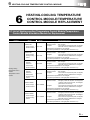
CHAPTER 6 HEATING-COOLING TEMPERATURE CONTROL MODULE/
TEMPERATURE CONTROL MODULE REPLACEMENT
6 - 1 to 6 - 53
6.1
List of Heating-cooling Temperature Control Module/Temperature Control Module Alternative Models
for Replacement .............................................................................................................................. 6 - 1
6.2
Performance Specifications Comparison ......................................................................................... 6 - 4
6.2.1
6.2.2
6.2.3
6.2.4
6.2.5
6.2.6
A1S64TCTRT(BW) (thermocouple connection) ....................................................................... 6 - 4
A1S64TCTRT(BW) (platinum resistance thermometer connection) ......................................... 6 - 8
A1S64TCTT(BW)-S1 .............................................................................................................. 6 - 12
A1S64TCRT(BW)-S1 (platinum resistance thermometer connection) ................................... 6 - 16
A1S62TCTT(BW)-S2 .............................................................................................................. 6 - 20
A1S62TCRT(BW)-S2 ............................................................................................................. 6 - 24
6.3
Functional Comparison .................................................................................................................. 6 - 28
6.4
I/O Signal Comparison ................................................................................................................... 6 - 30
6.4.1
6.4.2
6.4.3
6.4.4
6.5
A1S64TCTRT(BW) and Q series modules (standard control) ................................................ 6 - 30
A1S64TCTRT(BW) and Q series modules (heating-cooling control) ..................................... 6 - 32
A1S64TCTT(BW)-S1/A1S64TCRT(BW)-S1 and Q series modules ....................................... 6 - 34
A1S62TCTT(BW)-S2/A1S62TCRT(BW)-S2 and Q series modules ....................................... 6 - 36
Buffer Memory Address Comparison ............................................................................................. 6 - 38
6.5.1
6.5.2
6.5.3
6.5.4
A1S64TCTRT(BW) and Q series modules (standard control) ................................................ 6 - 38
A1S64TCTRT(BW) and Q series modules (heating-cooling control) ..................................... 6 - 42
A1S64TCTT(BW)-S1/A1S64TCRT(BW)-S1 and Q series modules ....................................... 6 - 46
A1S62TCTT(BW)-S2/A1S62TCRT(BW)-S2 and Q series modules ....................................... 6 - 50
CHAPTER 7 HIGH-SPEED COUNTER MODULE REPLACEMENT
7 - 1 to 7 - 26
7.1
List of High-Speed Counter Module Alternative Models for Replacement ....................................... 7 - 1
7.2
A1SD61 ........................................................................................................................................... 7 - 5
7.2.1
7.2.2
7.2.3
7.2.4
7.3
Performance specifications comparison ................................................................................... 7 - 5
Functional comparison ........................................................................................................... 7 - 11
I/O signal comparison ............................................................................................................. 7 - 12
Buffer memory address comparison ....................................................................................... 7 - 14
A1SD62(E/D/D-S1) ........................................................................................................................ 7 - 15
7.3.1
7.3.2
7.3.3
7.3.4
Performance specifications comparison ................................................................................. 7 - 15
Functional comparison ........................................................................................................... 7 - 23
I/O signal comparison ............................................................................................................. 7 - 24
Buffer memory address comparison ....................................................................................... 7 - 26
A - 11
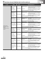
CHAPTER 8 POSITIONING MODULE REPLACEMENT
8 - 1 to 8 - 55
8.1
List of Positioning Module Alternative Models for Replacement ...................................................... 8 - 1
8.2
A1SD75P1-S3/P2-S3/P3-S3 ........................................................................................................... 8 - 3
8.2.1
8.2.2
8.2.3
8.2.4
8.2.5
8.3
A1SD75M1/M2/M3 ........................................................................................................................ 8 - 21
8.3.1
8.3.2
8.3.3
8.3.4
8.3.5
8.4
Performance specifications comparison ................................................................................... 8 - 3
Functional comparison .............................................................................................................. 8 - 8
I/O signal comparison ............................................................................................................. 8 - 11
Buffer memory address comparison ....................................................................................... 8 - 12
External interface specifications comparison .......................................................................... 8 - 20
Performance specifications comparison ................................................................................. 8 - 21
Functional comparison ............................................................................................................ 8 - 25
I/O signal comparison ............................................................................................................. 8 - 28
Buffer memory address comparison ....................................................................................... 8 - 29
External interface specifications comparison .......................................................................... 8 - 41
A1SD70 ......................................................................................................................................... 8 - 44
8.4.1
8.4.2
8.4.3
8.4.4
8.4.5
8.4.6
Performance specifications comparison ................................................................................. 8 - 44
Function comparison .............................................................................................................. 8 - 46
I/O signals comparison ........................................................................................................... 8 - 50
Buffer memory address comparison ....................................................................................... 8 - 51
Interface specifications comparison with external devices ..................................................... 8 - 53
Precautions for the replacement of the A1SD70 by the QD73A1 ........................................... 8 - 54
CHAPTER 9 POSITION DETECTION MODULE REPLACEMENT
9.1
9 - 1 to 9 - 2
Position Detection Module Replacement ......................................................................................... 9 - 1
CHAPTER 10 REPLACEMENT OF OTHER MODULES
10 - 1 to 10 - 2
10.1 Replacement of Other Modules ..................................................................................................... 10 - 1
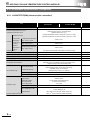
CHAPTER 11 EXTERNAL DIMENSIONS
11 - 1 to 11 - 2
11.1 External Dimensions ...................................................................................................................... 11 - 1
APPENDICES
App - 1 to App - 8
Appendix 1 Spare Parts Storage ..........................................................................................................App - 1
Appendix 2 Relevant Manuals ..............................................................................................................App - 2
Appendix 2.1
Appendix 2.2
Appendix 2.3
Appendix 2.4
Replacement handbooks ............................................................................................App - 2
AnS series ..................................................................................................................App - 3
Q series ......................................................................................................................App - 4
Programming tool .......................................................................................................App - 5
Appendix 3 How to Change Resolution After Analog I/O Module is Replaced .....................................App - 6
A - 12
● For the products shown in handbooks for transition, catalogues, and transition examples, refer to the
manuals for the relevant products and check the detailed specifications, precautions for use, and
restrictions before replacement.
For the products manufactured by Mitsubishi Electric Engineering Co., Ltd., Mitsubishi Electric
System & Service Co., Ltd., and other companies, refer to the catalogue for each product and check
the detailed specifications, precautions for use, and restrictions before use.
The manuals and catalogues for our products, products manufactured by Mitsubishi Electric
Engineering Co., Ltd., and Mitsubishi Electric System & Service Co., Ltd. are shown in Appendix of
each handbook for transition.
● Products shown in this handbook are subject to change without notice.
A - 13
GENERIC TERMS AND ABBREVIATIONS
Unless otherwise specified, this handbook uses the following generic terms and abbreviations.
Generic term/abbreviation
Series
A series
AnS series
A/AnS series
QnA series
QnAS series
QnA/QnAS series
A/AnS/QnA/QnAS series
Q series
CPU module type
CPU module
Basic model QCPU
High Performance model
QCPU
Process CPU
Redundant CPU
Description
Abbreviation for large types of Mitsubishi MELSEC-A series programmable controllers
Abbreviation for compact types of Mitsubishi MELSEC-A series programmable controllers
Generic term for A series and AnS series
Abbreviation for large types of Mitsubishi MELSEC-QnA series programmable controllers
Abbreviation for compact types of Mitsubishi MELSEC-QnA series programmable controllers
Generic term for QnA series and QnAS series
Generic term for A series, AnS series, QnA series, and QnAS series
Abbreviation for Mitsubishi MELSEC-Q series programmable controllers
Generic term for A series, AnS series, QnA series, QnAS series, and Q series CPU modules
Generic term for the Q00JCPU, Q00CPU, and Q01CPU
Generic term for the Q02CPU, Q02HCPU, Q06HCPU, Q12HCPU, and Q25HCPU
*
This handbook mainly explains about the Q02CPU, Q02HCPU, Q06HCPU, and Q12HCPU.
Generic term for the Q02PHCPU, Q06PHCPU, Q12PHCPU, and Q25PHCPU
Generic term for the Q12PRHCPU and Q25PRHCPU
Generic term for the Q00UJCPU, Q00UCPU, Q01UCPU, Q02UCPU, Q03UDCPU,
Q04UDHCPU, Q06UDHCPU, Q10UDHCPU, Q13UDHCPU, Q20UDHCPU, Q26UDHCPU,
Q03UDECPU, Q04UDEHCPU, Q06UDEHCPU, Q10UDEHCPU, Q13UDEHCPU,
Universal model QCPU
Q20UDEHCPU, Q26UDEHCPU, Q50UDEHCPU, and Q100UDEHCPU
*
This handbook mainly explains about the Q00UJCPU, Q00UCPU, Q01UCPU, Q02UCPU,
Q03UDCPU, Q04UDHCPU, and Q06UDHCPU, which can replace the AnS/QnAS series.
The specifications and functions of the Q10UDEHCPU to Q100UDEHCPU are the same as those of
the modules described above, although the program and memory capacities increase.
CPU module model
ACPU
AnSCPU
AnNCPU
AnACPU
AnUCPU
AnUS(H)CPU
A/AnSCPU
AnN/AnACPU
AnN/AnA/AnSCPU
QnACPU
QnASCPU
QnA/QnASCPU
A/AnS/QnA/QnASCPU
QCPU
A - 14
Generic term for MELSEC-A series programmable controller CPUs
Generic term for MELSEC-AnS series programmable controller CPUs
Generic term for the A1NCPU, A1NCPUP21/R21, A1NCPUP21-S3, A2NCPU, A2NCPU-S1,
A2NCPUP21/R21, A2NCPUP21/R21-S1, A2NCPUP21-S3(S4), A3NCPU, A3NCPUP21/R21,
and A3NCPUP21-S3
Generic term for the A2ACPU, A2ACPU-S1, A3ACPU, A2ACPUP21/R21, A2ACPUP21/R21S1, and A3ACPUP21/R21
Generic term for the A2UCPU, A2UCPU-S1, A3UCPU, A4UCPU, A2USCPU, A2USCPU-S1,
and A2USHCPU-S1
Generic term for the A2USCPU, A2USCPU-S1, A2USHCPU-S1
Generic term for MELSEC-A series and MELSEC-AnS series programmable controller CPUs
Generic term for the AnNCPU and AnACPU
Generic term for the AnNCPU, AnACPU, and AnSCPU
Generic term for MELSEC-QnA series programmable controller CPUs
Generic term for MELSEC-QnAS series programmable controller CPUs
Generic term for MELSEC-QnA series and MELSEC-QnAS series programmable controller
CPUs
Generic term for A series, AnS series, QnA series, and QnAS series programmable controller
CPUs
Generic term for MELSEC-Q series programmable controller CPUs
Memo
A - 15
1
INTRODUCTION
1
INTRODUCTION
1
1.1 Advantages of Transition to Q Series
Advantage 1)Advanced performance of equipments
In addition to the processing performance improvement for Q series CPU, the processing
speed for Q series intelligent function module is also increased, so that the equipment capability
to improve is possible.
Advantage 2)Compact control panel and space saving
As the Q series needs only 1/4 mounting area of the AnS/QnAS series, it is possible to create
more compact control panel.
Advantage 3)Improved operating efficiency for programming and monitor
Q series intelligent function module prepares the following utility package (GX Configurator-)
sold separately.
(Example)
•
•
•
•
•
GX Configurator-AD Analog input module setting/monitoring tool
GX Configurator-DA Analog output module setting/monitoring tool
GX Configurator-TI Temperature input module setting/monitoring tool
GX Configurator-CT High speed counter module setting/monitoring tool
GX Configurator-QP Positioning module setting/monitoring tool
Using the utility package is not a must. However, the utility package allows not only for the
followings to do, but also reduces sequence programs.
• Initial setting is possible without a program.
• The auto refresh setting allows to read/write buffer memory data of intelligent function module
automatically from/to the CPU device memory.
• Checking of the setting status or operating status of intelligent function module is simplified.
1-1
1
INTRODUCTION
1.2 Precautions for Transition from AnS/QnAS Series to Q Series
(1) Be sure to confirm its functions, specifications and instructions by referring the manual of the
corresponding Q series module prior to use.
(2) Be sure to check the operation of whole system before the actual operation.
1-2
2
ANALOG INPUT MODULE REPLACEMENT
2
ANALOG INPUT MODULE
REPLACEMENT
2
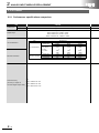
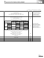
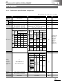
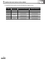
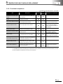
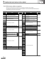
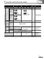
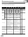
2.1 List of Analog Input Module Alternative Models for Replacement
AnS/QnAS series
Product
Model
A1S64AD
Transition to Q series
Model
Q64AD
Remarks (Restrictions)
1) External wiring
2) Number of slots
3) Program
: Cable size is changed.
: Not changed
: The number of occupied I/O points, I/O signals, and buffer
memory addresses are changed.
4) Performance specifications: Not changed
5) Functional specifications: Not changed
1) External wiring
2) Number of slots
3) Program
Q68ADV
Q68ADI
Analog input module
A1S68AD
1) External wiring
2) Number of slots
3) Program
Q68AD-G*1
*1
2-1
: Cable size is changed.
: Not changed
: The number of occupied I/O points, I/O signals, and buffer
memory addresses are changed.
4) Performance specifications:
Input signals (either V or I input) and I/O characteristics are
changed.
5) Functional specifications: Not changed
: Cable size is changed.
: Not changed
: The number of occupied I/O points, I/O signals, and buffer
memory addresses are changed.
4) Performance specifications:
Changed. Conversion speed (0.5ms/channel) sampling
cycle (10ms/channel) + response speed (20ms)
5) Functional specifications: Changed (Non-insulation insulation between
channels)
The Q68AD-G cannot be mounted on the Q series large type base unit (Q3BL, Q6BL, Q55BL).
2
ANALOG INPUT MODULE REPLACEMENT
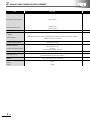
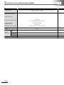
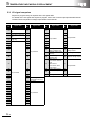
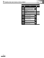
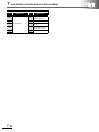
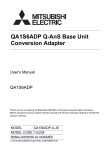
Point
The existing wiring for the AnS/QnAS series modules can be connected directly to the Q series modules
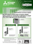
using the upgrade tool (conversion adaptor) manufactured by Mitsubishi Electric Engineering Co., Ltd.
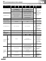
Product
Analog input module
MELSEC-AnS/QnAS
series module
A1S64AD
A1S68AD
MELSEC-Q
series module
Q64AD
Q68ADV
Q68ADI
Q68AD-G
*1
Conversion adaptor
ERNT-ASQT64AD
ERNT-ASQT68AD
ERNT-ASQT68AD-G*1
Conversion adapter with fixture, which cannot be mounted on the AnS size version Q large type base unit.
Before using the conversion adapter with fixture, be sure to fasten its fixture to the base adapter or DIN rail mounting
bracket using screws.
For MELSEC-AnS/QnAS (small type) series to Q series transition related products manufactured by Mitsubishi
Electric Engineering Co., Ltd. or Mitsubishi Electric System & Service Co., Ltd., contact your local sales office or
representative.
2-2
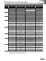
2
ANALOG INPUT MODULE REPLACEMENT
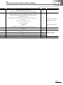
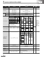
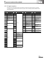
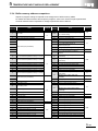
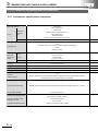
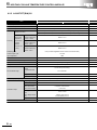
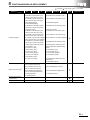
2.2 A1S64AD
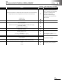
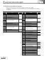
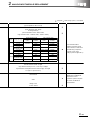
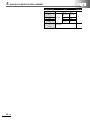
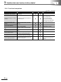
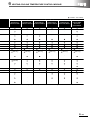
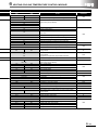
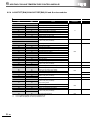
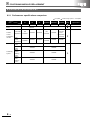
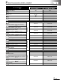
2.2.1 Performance specifications comparison
Item
Analog input
A1S64AD
Voltage
-10 to 0 to +10VDC (Input resistance value: 1M)
Current
-20 to 0 to +20mADC (Input resistance value: 250)
16-bit signed binary
When 1/4000 is set: -4096 to +4095
Digital output
When 1/8000 is set: -8192 to +8191
When 1/12000 is set: -12288 to +12287
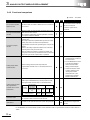
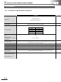
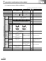
Item
Specifications
I/O characteristics
Analog input
I/O characteristics
Maximum resolution
Overall accuracy
(Accuracy in respect to
maximum digital output value)
2-3
+10V
+5V or +20mA
0V or 0mA
-5V or -20mA
-10V
Maximum resolution
±1%
When 1/4000 is set: ±40
When 1/8000 is set: ±80
When 12000 is set: ±120
Digital output value (when gain 5V/20mA, offset 0V/0mA)
1/4000
1/8000
1/12000
+4000
+2000
0
-2000
-4000
+8000
+4000
0
-4000
-8000
+12000
+6000
0
-6000
-12000
Analog input
1/4000
1/8000
1/12000
Voltage input
2.5mV
1.25mV
0.83mV
Current input
10µA
5µA
3.33µA
2
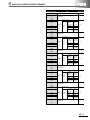
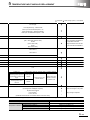
ANALOG INPUT MODULE REPLACEMENT
: Compatible,
Q64AD
: Partial change required, ×: Incompatible
Compatibility Precautions for replacement
-10 to 10VDC (Input resistance value: 1M)
0 to 20mADC (Input resistance value: 250)
16-bit signed binary
(Normal resolution mode: -4096 to 4095,
High resolution mode: -12288 to 12287, -16384 to 16383)
If the resolution differs
Normal resolution mode
Analog input
range
Digital
output value
0 to 10V
0 to 5V
0 to 4000
Voltage
-10 to 10V
0 to 20mA
Current
Digital
output value
Maximum
resolution
series modules, it needs to be
2.5mV
0 to 16000
0.625mV
program or user range
0.416mV
settings. (Refer to Appendix 3.)
1.0mV
User range
settings
4 to 20mA
User range
settings
-4000 to 4000
0.625mV
0.375mV
-12000 to 12000
0.333mV
1.37µA
Normal resolution mode
Analog input
range
Ambient temperature
0 to 55°C
-12000 to 12000
1.66µA
1.33µA
1.33µA
High resolution mode
Ambient temperature
0 to 55°C
Ambient
Ambient
With
Without
With
Without
temperature
temperature
temperature temperature
temperature temperature
25±5°C
25±5°C
drift
drift
drift
drift
compensation compensation
compensation compensation
0 to 10V
-10 to
10V
Voltage
0 to 12000
matched using a sequence
0.333mV
-16000 to 16000
4µA
-4000 to 4000
0 to 12000
2.5mV
5µA
0 to 4000
between AnS series and Q
Maximum
resolution
1.25mV
1 to 5V
High resolution mode
±0.3%
(±48 digits)
±0.4%
(±64 digits)
±0.1%
(±16 digits)
±0.3%
(±36 digits)
±0.4%
(±48 digits)
±0.1%
(±12 digits)
0 to 5V
1 to 5V
User
range
settings
0 to
20mA
±0.3%
(±12 digits)
±0.4%
(±16 digits)
±0.1%
(±4 digits)
4 to
Current 20mA
User
range
settings
2-4
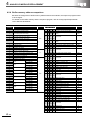
2
ANALOG INPUT MODULE REPLACEMENT
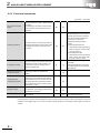
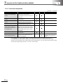
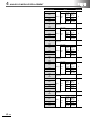
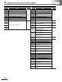
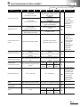
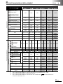
Item
Maximum conversion speed
Absolute maximum input
Analog input points
Maximum number of writes for
E2PROM
Isolation method
Dielectric withstand voltage
Insulation resistance
Number of occupied I/O points
Connected terminal
Applicable wire size
Applicable solderless
terminal
Internal current consumption
(5VDC)
Weight
2-5
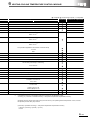
A1S64AD
20ms/channel
Voltage: ±15V
Current: ±30mA
4 channels/module
Between the input terminal and programmable controller power supply: photocoupler isolation
Between channels: not isolated
Between the input terminal and programmable controller power supply:
500VAC, for 1 minute
Between the input terminal and programmable controller power supply:
500VDC, 5M or more
32 points
(I/O assignment: special 32 points)
20-point terminal block
0.75 to 1.5mm2
(Applicable tightening torque: 39 to 59N•cm)
1.25-3, 1.25-YS3, V1.25-3, V1.25-YS3A
0.40A
0.25kg
2
ANALOG INPUT MODULE REPLACEMENT
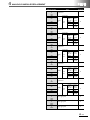
: Compatible,
Q64AD
Compatibility
: Partial change required, ×: Incompatible
Precautions for replacement
The conversion speed of Q64AD to
A1S64AD has become quick. And
then, on A1S64AD, the noise that did
80µs/channel (When there is temperature drift compensation, the time calculated by
not import on A1S64AD can be
adding 160µs will be used regardless of the number of channels used.)
imported as analog signal.
In this case, use the averaging
processing function to remove the
effect of noise.
Voltage: ±15V
Current: ±30mA
4 channels/module
Max. 100,000 times
Between the I/O terminal and programmable controller power supply:
photocoupler isolation
Between channels: not isolated
Between the I/O terminal and programmable controller power supply:
500VAC, for 1 minute
Between the I/O terminal and programmable controller power supply:
500VDC, 20M or more
16 points
The number of occupied I/O points
(I/O assignment: intelligent 16 points)
has changed to 16 points.
18-point terminal block
×
0.3 to 0.75mm2
×
R1.25-3
(Solderless terminals with an insulation sleeve cannot be used.)
0.63A
Wiring change is required.
×
Recalculation of internal current
consumption (5VDC) is required.
0.18kg
2-6
2
ANALOG INPUT MODULE REPLACEMENT
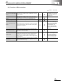
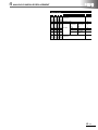
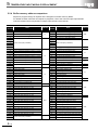
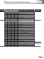
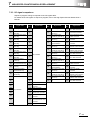
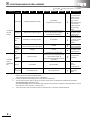
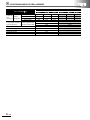
2.2.2 Functional comparison
: Available, -: Not available
Item
Description
A1S64AD
Q64AD
Precautions for replacement
Specifies whether to enable or disable the A/D
A/D conversion enable/
disable
conversion.
By disabling the conversion for the channels
that are not used, the sampling time can be
shortened.
The sampling processing time
changes depending on the number of
channels used (number of channels
set to A/D conversion enable) and
whether, with or without the
temperature drift compensation
The A/D conversion for analog input values is
Sampling processing
function.
performed successively for each channel, and
(a) Without temperature drift
the digital output value is output upon each
compensation function (processing
conversion.
time) = (number of channels used)
× 80 (µs/1 channel)
(b) With temperature drift
compensation function (processing
time)= (number of channels used)
× 80 (µs/1 channel) +160µs
The setting range of average time and
For each channel, A/D conversion values are
Averaging processing
count differ.
averaged for the set number of times or set
Check the specifications, referring to
amount of time, and the average value is
the Analog-Digital Converter Module
output as a digital value.
Maximum and minimum
values hold function
User's Manual.
The maximum and minimum values of the
digital output values are retained in the
-
module.
Errors arising from changes in the ambient
temperature of the module are automatically
Temperature drift
compensated to improve conversion accuracy.
compensation function
The temperature drift compensation function
-
can be performed at (A/D conversion time for
all channels) + 160µs.
The resolution can be switched according to
the application. The resolution mode setting is
Resolution mode
applicable to all channels.*1
Online module change
*1
A module can be replaced without the system
being stopped.
-
The Process CPU and Redundant
CPU support this function.
For the A1S64AD, the resolution for both voltage and current can be selected from 1/4000, 1/8000, or 1/12000.
For the Q64AD, the resolution for both voltage and current is 1/4000 in normal resolution mode. In high resolution mode, the
resolution for the voltage range -10 to 0 to 10V is 1/16000, and the resolution for the voltage in other ranges and current is
1/12000.
2-7
2
ANALOG INPUT MODULE REPLACEMENT
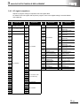
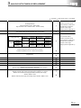
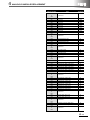
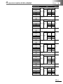
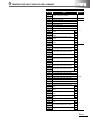
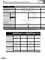
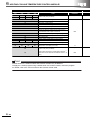
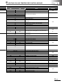
2.2.3 I/O signal comparison
Sequence program change is required as the I/O signals differ.
For details of the I/O signals or sequence program, refer to the Analog-Digital Converter Module User's
Manual.
A1S64AD
Device
No.
X0
Signal name
Watchdog timer error
Device
No.
Q64AD
Signal name
Y0
Device
Signal name
No.
X0
X1
A/D conversion READY
Y1
X1
X2
Error flag
Module READY
Temperature drift
compensation flag
Device
No.
Y0
Y1
Y2
X2
Y2
X3
Y3
X3
Y3
X4
Y4
X4
X5
Y5
X5
X6
Y6
X6
X7
Y7
X7
X8
Y8
X8
X9
Y9
X9
Use prohibited
XA
YA
XA
XB
YB
XB
XC
YC
XC
Use prohibited
Y4
YD
XD
Y6
Y7
High resolution mode
status flag
Operating condition
setting completed flag
Offset/gain setting mode
flag
Channel change
completed flag
Use prohibited
Y8
Y9
YA
minimum value reset
Use prohibited
YE
XE
XF
YF
XF
X10
Y10
X11
Y11
X12
Y12
X13
Y13
X14
Y14
X15
Y15
X16
Y16
X17
Y17
X18
Y18
X19
Y19
X1A
Y1A
X1B
Y1B
X1C
Y1C
X1D
Y1D
X1E
Y1E
X1F
Y1F
A/D conversion
completed flag
Error flag
Operating condition
setting request
User range writing
request
YB
Channel change request
YC
Use prohibited
Maximum value/
YD
completed flag
XE
Use prohibited
Y5
Maximum value/
XD
Signal name
minimum value reset
request
YE
Use prohibited
YF
Error clear request
Error reset
Use prohibited
2-8
2
ANALOG INPUT MODULE REPLACEMENT
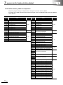
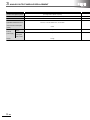
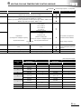
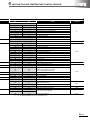
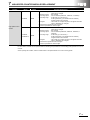
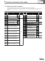
2.2.4 Buffer memory address comparison
Sequence program change is required as the assignment of buffer memory differs.
For details of the buffer memory or sequence program, refer to the Analog-Digital Converter Module
User's Manual.
A1S64AD
Address
Name
(decimal)
Q64AD
Read/write
Address
Name
(decimal)
0
A/D conversion enable/disable setting
0
A/D conversion enable/disable setting
1
Average processing specification
1
CH1 Average time/average number of times
2
CH1 Average time, count
2
CH2 Average time/average number of times
3
CH2 Average time, count
3
CH3 Average time/average number of times
4
CH3 Average time, count
4
CH4 Average time/average number of times
5
CH4 Average time, count
5
R/W
6
7
8
6
System area (Use prohibited)
-
9
10
CH1 Digital output value
11
CH2 Digital output value
12
CH3 Digital output value
13
CH4 Digital output value
-
9
Averaging processing setting
R/W
10
A/D conversion completed flag
8
11
CH1 Digital output value
CH2 Digital output value
13
CH3 Digital output value
14
14
CH4 Digital output value
15
15
16
System area (Use prohibited)
-
17
16
17
18
Write data error code
19
A-D conversion completed flag
20
Resolution setting
R
R/W
System area (Use prohibited)
R
-
18
19
Error code
20
Setting range (CH1 to CH4)
21
System area (Use prohibited)
22
Offset/gain setting mode Offset specification
23
Offset/gain setting mode Gain specification
24 to 29 System area (Use prohibited)
30
31
CH1 Minimum value
32
CH2 Maximum value
33
CH2 Minimum value
34
CH3 Maximum value
35
CH3 Minimum value
36
CH4 Maximum value
37
CH4 Minimum value
158
159
160 to
R
R/W
-
CH1 Maximum value
38 to 157 System area (Use prohibited)
Mode switching setting
R
R/W
System area (Use prohibited)
-
200
Pass data classification setting
R/W
201
System area (Use prohibited)
-
202
CH1 Industrial shipment settings offset value
199
2-9
R/W
System area (Use prohibited)
7
12
R
Read/write
203
CH1 Industrial shipment settings gain value
204
CH2 Industrial shipment settings offset value
205
CH2 Industrial shipment settings gain value
206
CH3 Industrial shipment settings offset value
207
CH3 Industrial shipment settings gain value
208
CH4 Industrial shipment settings offset value
209
CH4 Industrial shipment settings gain value
R/W
2
ANALOG INPUT MODULE REPLACEMENT
Q64AD
Address
(decimal)
Name
210
CH1 User range settings offset value
211
CH1 User range settings gain value
212
CH2 User range settings offset value
213
CH2 User range settings gain value
214
CH3 User range settings offset value
215
CH3 User range settings gain value
216
CH4 User range settings offset value
217
CH4 User range settings gain value
Read/write
R/W
2 - 10
2
ANALOG INPUT MODULE REPLACEMENT
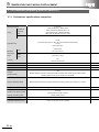
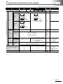
2.3 A1S68AD (Replacing with the Q68ADV or Q68ADI)
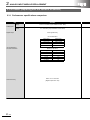
2.3.1 Performance specifications comparison
Item
A1S68AD
Voltage
-10 to 0 to +10VDC (Input resistance value: 1M)
Current
0 to +20mADC (Input resistance value: 250)
Analog input
Digital output
16-bit signed binary
I/O characteristics
Analog input
I/O characteristics,
maximum resolution
Overall accuracy
2 - 11
Digital output
0 to +10V
0 to +4000
-10V to +10V
-2000 to +2000
0V to 5V or 0 to 20mA
0 to +4000
1 to 5V or 4 to 20mA
0 to +4000
Maximum resolution
Analog input
Digital output
0 to +10V
2.5mV
-10V to +10V
5mV
0V to 5V
1.25mV
1 to 5V
1mV
0 to 20mA
5µA
4 to 20mA
4µA
Within ±1% at full scale
(Digital output value: ±40)
2
ANALOG INPUT MODULE REPLACEMENT
: Compatible,
Q68ADV
Q68ADI
-10 to 10VDC
-
(Input resistance value: 1M)
The voltage/current cannot be
0 to 20mADC
-
: Partial change required, ×: Incompatible
Compatibility Precautions for replacement
mixed for one module.
(Input resistance value: 250)
16-bit signed binary
(Normal resolution mode: -4096 to 4095,
High resolution mode: -12288 to 12287, -16384 to 16383)
Normal resolution mode
Analog input
range
Maximum
resolution
Digital output
value
Maximum
resolution
2.5mV
0 to 16000
0.625mV
0 to 4000
1.25mV
0 to 10V
0 to 5V
Voltage
1 to 5V
1.0mV
-10 to 10V
2.5mV
0.375mV
User range
settings
0 to 20mA
Current
-4000 to 4000
5µA
0 to 4000
4 to 20mA
User range
settings
4µA
-4000 to 4000
1.37µA
Normal resolution mode
Analog input
range
Ambient temperature
0 to 55°C
0.416mV
If the resolution differs
0.333mV
between AnS series and Q
-16000 to 16000
0.625mV
series modules, it needs to be
-12000 to 12000
0.333mV
matched using a sequence
0 to 12000
0 to 12000
-12000 to 12000
1.66µA
1.33µA
program or user range
settings. (Refer to Appendix 3.)
1.33µA
High resolution mode
Ambient temperature
0 to 55°C
Ambient
Ambient
With
Without
With
Without
temperature
temperature
temperature temperature
temperature temperature
25±5°C
25±5°C
drift
drift
drift
drift
compensation compensation
compensation compensation
0 to 10V
-10 to
10V
Voltage
High resolution mode
Digital output
value
±0.3%
(±48 digits)
±0.4%
(±64 digits)
±0.1%
(±16 digits)
±0.3%
(±36 digits)
±0.4%
(±48 digits)
±0.1%
(±12 digits)
0 to 5V
1 to 5V
user
range
settings
0 to
20mA
±0.3%
(±12 digits)
±0.4%
(±16 digits)
±0.1%
(±4 digits)
4 to
Current 20mA
user
range
settings
2 - 12
2
ANALOG INPUT MODULE REPLACEMENT
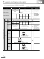
Item
Maximum conversion speed
Absolute maximum input
Analog input points
Maximum number of writes for
E2PROM
Isolation method
A1S68AD
0.5ms/channel
(The speed is 1ms/channel on all channels if averaging processing is set even for one channel.)
Voltage: ±35V
Current: ±30mA
8 channels/module
Between the input terminal and programmable controller power supply: photocoupler isolation
Between channels: not isolated
Dielectric withstand voltage
-
Insulation resistance
-
Number of occupied I/O points
32 points
(I/O assignment: special 32 points)
Connected terminal
20-point terminal block
Applicable wire size
0.75 to 1.5mm2
Applicable solderless
terminal
Internal current consumption
(5VDC)
Weight
2 - 13
R1.25-3, 1.25-YS3, RAV1.25-3, V1.25-YS3A
0.40A
0.27kg
2
ANALOG INPUT MODULE REPLACEMENT
: Compatible,
Q68ADV
Q68ADI
Compatibility
: Partial change required, ×: Incompatible
Precautions for replacement
The conversion speed of Q68ADV/I
to A1S68AD has become quick. And
80µs/channel
then, on A1S68AD, the noise that did
(When there is temperature drift compensation, the time calculated by adding 160µs
not import on A1S68AD can be
will be used regardless of the number of channels used.)
imported as analog signal. In this
case, use the averaging processing
function to remove the effect of noise.
±15V
±30mA
8 channels/module
Max. 100,000 times
Between the I/O terminal and programmable controller power supply:
photocoupler isolation
Between channels: not isolated
Between the I/O terminal and programmable controller power supply:
500VAC, for 1 minute
Between the I/O terminal and programmable controller power supply:
500VDC, 20M or more
16 points
The number of occupied I/O points
(I/O assignment: intelligent 16 points)
has changed to 16 points.
18-point terminal block
×
0.3 to 0.75mm2
×
R1.25-3 (Solderless terminals with an insulation sleeve cannot be used.)
×
0.64A
0.64A
0.19kg
0.19kg
Wiring change is required.
Recalculation of internal current
consumption (5VDC) is required.
2 - 14
2
ANALOG INPUT MODULE REPLACEMENT
2.3.2 Functional comparison
: Available, -: Not available
Item
Description
A1S68AD
Q68ADV/I
Precautions for replacement
Specifies whether to enable or disable the
A/D conversion for each channel.
A/D conversion enable/disable
By disabling the conversion for the
channels that are not used, the sampling
time can be shortened.
The sampling processing time
changes depending on the
number of channels used
(number of channels set to A/D
conversion enable) and whether,
with or without the temperature
drift compensation function.
The A/D conversion for analog input values
Sampling processing
(a) Without temperature drift
is performed successively for each channel,
compensation function
and the digital output value is output upon
(processing time) =
each conversion.
(number of channels used) ×
80 (µs/1 channel)
(b) With temperature drift
compensation function
(processing time) =
(number of channels used) ×
80 (µs/1 channel) + 160µs
The setting range of average
Averaging processing
For each channel, A/D conversion values
time and count differ.
are averaged for the set number of times or
Check the specifications,
set amount of time, and the average value
referring to the Analog-Digital
is output as a digital value.
Converter Module User's
Manual.
Maximum and minimum values
hold function
The maximum and minimum values of the
digital output values are retained in the
-
module.
Errors arising from changes in the ambient
temperature of the module are
automatically compensated for to improve
Temperature drift
compensation function
conversion accuracy.
-
The temperature drift compensation
function can be performed at (A/D
conversion time for all channels) + 160µs.
The resolution can be switched according to
the application. The resolution mode setting
Resolution mode
is applicable to all channels.
Online module change
*1
-
*1
A module can be replaced without the
system being stopped.
The Process CPU and
-
Redundant CPU support this
function.
For the A1S68AD, the resolution is 1/4000 (fixed).
For the Q68ADV/I, the resolution for both voltage and current is 1/4000 in normal resolution mode. In high resolution mode,
the resolution for the voltage range -10 to 0 to 10V is 1/16000, and the resolution for the voltage in other ranges and current
is 1/12000.
2 - 15
2
ANALOG INPUT MODULE REPLACEMENT
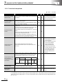
2.3.3 I/O signal comparison
Sequence program change is required as the I/O signals differ.
For details of the I/O signals or sequence program, refer to the Analog-Digital Converter Module User's
Manual.
A1S68AD
Device
No.
X0
Signal name
WDT error flag
Device
No.
Q68ADV/I
Signal name
Y0
Device
Signal name
No.
X0
X1
A-D conversion READY
Y1
X1
X2
Error flag
Module READY
Temperature drift
compensation flag
Device
No.
Y0
Y1
Y2
X2
Y2
X3
Y3
X3
Y3
X4
Y4
X4
X5
Y5
X5
X6
Y6
X6
X7
Y7
X7
X8
Y8
X8
X9
Y9
X9
Use prohibited
XA
YA
XA
XB
YB
XB
XC
YC
XC
Use prohibited
Y4
YD
XD
Y6
Y7
High resolution mode
status flag
Operating condition
setting completed flag
Offset/gain setting mode
flag
Channel change
completed flag
Use prohibited
Y8
Y9
YA
minimum value reset
Use prohibited
YE
XE
XF
YF
XF
X10
Y10
X11
Y11
X12
Y12
X13
Y13
X14
Y14
X15
Y15
X16
Y16
X17
Y17
X18
Y18
X19
Y19
X1A
Y1A
X1B
Y1B
X1C
Y1C
X1D
Y1D
X1E
Y1E
X1F
Y1F
A/D conversion
completed flag
Error flag
Operating condition
setting request
User range writing
request
YB
Channel change request
YC
Use prohibited
Maximum value/
YD
completed flag
XE
Use prohibited
Y5
Maximum value/
XD
Signal name
minimum value reset
request
YE
Use prohibited
YF
Error clear request
Error reset
Use prohibited
2 - 16
2
ANALOG INPUT MODULE REPLACEMENT
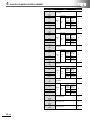
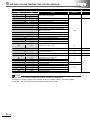
2.3.4 Buffer memory address comparison
Sequence program change is required as the assignment of buffer memory differs.
For details of the buffer memory or sequence program, refer to the Analog-Digital Converter Module
User's Manual.
A1S68AD
Address
(decimal)
Name
0
A-D conversion enable/disable
1
Writing data error code
2
Average processing specification
Q68ADV/I
Read/write
Address
Name
(decimal)
R/W
0
A/D conversion enable/disable setting
R
1
CH1 Average time/average number of times
R/W
2
CH2 Average time/average number of times
3
3
CH3 Average time/average number of times
to
to
8
System area (Use prohibited)
-
9
8
CH8 Average time/average number of times
9
Averaging process setting
10
CH1 Average time, count
10
A/D conversion completed flag
11
CH2 Average time, count
11
CH1 Digital output value
to
17
18
19
R/W
CH8 Average time, count
System area (Use prohibited)
-
R/W
to
17
CH7 Digital output value
18
CH8 Digital output value
19
Error code
20
CH1 Digital output value
20
Setting range (CH1 to CH4)
21
CH2 Digital output value
21
Setting range (CH5 to CH8)
22
CH3 Digital output value
22
Offset/gain setting mode Offset specification
23
CH4 Digital output value
23
Offset/gain setting mode Gain specification
24
CH5 Digital output value
25
CH6 Digital output value
25
26
CH7 Digital output value
26
27
CH8 Digital output value
27
28
A-D conversion completed flag
29
System area (Use prohibited)
R
Read/write
R
R/W
24
R/W
28
-
29
System area (Use prohibited)
30
CH1 Maximum value
31
CH1 Minimum value
to
-
R
44
CH8 Maximum value
45
CH8 Minimum value
46
to
System area (Use prohibited)
-
157
158
159
Mode switching setting
R/W
160
to
System area (Use prohibited)
-
201
202
CH1 Industrial shipment settings offset value
203
CH1 Industrial shipment settings gain value
to
216
CH8 Industrial shipment settings offset value
217
CH8 Industrial shipment settings gain value
218
CH1 User range settings offset value
219
CH1 User range settings gain value
to
2 - 17
232
CH8 User range settings offset value
233
CH8 User range settings gain value
R/W
2
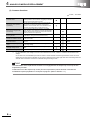
ANALOG INPUT MODULE REPLACEMENT
Memo
2 - 18
2
ANALOG INPUT MODULE REPLACEMENT
2.4 A1S68AD (Replacing with the Q68AD-G)
2.4.1 Performance specifications comparison
Item
A1S68AD
Voltage
-10 to 0 to +10VDC (Input resistance value: 1M)
Current
0 to +20mADC (Input resistance value: 250)
Analog input
Digital output
16-bit signed binary
I/O characteristics
Analog input
I/O characteristics,
Digital output
0 to +10V
0 to +4000
-10V to +10V
-2000 to +2000
0V to 5V or 0 to 20mA
0 to +4000
1 to 5V or 4 to 20mA
0 to +4000
Maximum resolution
maximum resolution
Reference
Overall
accuracy
Analog input
Digital output
0 to +10V
2.5mV
-10V to +10V
5mV
0V to +5V
1.25mV
1 to 5V
1mV
0 to 20mA
5µA
4 to 20mA
4µA
Within ±1% at full scale
(Digital output value: ±40)
accuracy
Temperature
coefficient
Maximum conversion speed
0.5ms/channel
(sampling cycle)
(The speed is 1ms/channel on all channels if averaging processing is set even for one channel.)
Response time
-
Absolute maximum input
2 - 19
Voltage: ±35V
current: ±30mA
2
ANALOG INPUT MODULE REPLACEMENT
: Compatible,
Q68AD-G
: Partial change required, ×: Incompatible
Compatibility Precautions for replacement
-10 to 10VDC
(Input impedance: 1M or more)
0 to 20mADC
(Input resistance value: 250)
16-bit signed binary
(Normal resolution mode: -4096 to 4095,
High resolution mode: -12288 to 12287, -16384 to 16383)
Normal resolution mode
Input
Analog input range
Maximum
resolution
Digital output
value
Maximum
resolution
2.5mV
0 to 16000
0.625mV
0 to 4000
1.25mV
0 to 10V
0 to 5V
1 to 5V
Voltage
1 to 5V
(Expanded mode)
-10 to 10V
Users range setting
0 to 20mA
4 to 20mA
Current
High resolution mode
Digital output
value
0 to 12000
1.0mV
-1000 to 4500
-4000 to 4000
0.416mV
0.333mV
If the resolution differs
between AnS series and Q
1.0mV
-3000 to 13500
0.333mV
series modules, it needs to be
2.5mV
-16000 to 16000
0.625mV
matched using a sequence
0.375m V
-12000 to 12000
0.333mV
program or user range
5µA
0 to 4000
0 to 12000
4µA
1.66µA
settings. (Refer to Appendix 3.)
1.33µA
4 to 20mA
(Expanded mode)
-1000 to 4500
4µA
-3000 to 13500
1.33µA
Users range setting
-4000 to 4000
1.37µA
-12000 to 12000
1.33µA
Reference accuracy: ±0.1%
Normal resolution mode: ±4 digits
High resolution mode (0 to 10V, -10 to 10V): ±16 digits
High resolution mode (Other than the above ranges): ±12 digits
±71.4ppm/°C (0.00714%/°C)
10ms/channel
The conversion speed of
Q68AD-G to A1S68AD has
become slow. If fast
20ms
conversion speed is required
for control, the Q64AD is
recommended.
Voltage: ±15V
current: ±30mA
2 - 20
2
ANALOG INPUT MODULE REPLACEMENT
Item
Analog input points
Maximum number of writes for
E2PROM
Isolation method
A1S68AD
8 channels/module
Between the input terminal and programmable controller power supply: photocoupler isolation
Between channels: not isolated
Dielectric withstand voltage
-
Insulation resistance
-
Number of occupied I/O points
32 points
(I/O assignment: special 32 points)
Connected terminal
20-point terminal block
Applicable wire size
0.75 to 1.5mm2
Applicable solderless terminal
Internal current consumption
(5VDC)
Weight
2 - 21
R1.25-3, 1.25-YS3, RAV1.25-3, V1.25-YS3A
0.4A
0.27kg
2
ANALOG INPUT MODULE REPLACEMENT
: Compatible,
Q68AD-G
: Partial change required, ×: Incompatible
Compatibility Precautions for replacement
8 channels/module
Up to 50,000 times
Between the input terminal and programmable controller power supply: transformer isolation
Between channels: transformer isolation
Between the input terminal and programmable controller power supply:
500VACrms, for 1 minute
Between channels: 1000VACrms, for 1 minute
Between the input terminal and programmable controller power supply:
500VDC, 10M or more
Between channels: 500VDC, 10M or more
The number of occupied I/O
16 points
points has changed to 16
(I/O assignment: intelligent, 16 points)
40-pin connector
2
points.
×
Within 0.3mm
×
-
×
Wiring change is required.
Recalculation of internal
0.46A
current consumption (5VDC) is
required.
0.16kg
2 - 22
2
ANALOG INPUT MODULE REPLACEMENT
2.4.2 Functional comparison
: Available, -: Not available
Item
Description
A1S68AD
Q68AD-G
Precautions for replacement
Specifies whether to enable or disable the
A/D conversion for each channel.
A/D conversion enable/disable
By disabling the conversion for the
channels that are not used, the sampling
time can be shortened.
The A/D conversion for analog input values
Sampling processing
is performed successively for each channel,
and the digital output value is output upon
each conversion.
For each channel, A/D conversion values
The setting range of average
are averaged for the set number of times or
time and count differ.
set amount of time, and the average value
Averaging processing
Check the specifications,
is output as a digital value.
referring to the Analog-Digital
Moving average takes the average of the
specified number of digital output values
-
measured per sampling time.
Maximum and minimum values
hold function
Converter Module User's
Manual.
The maximum and minimum values of the
digital output values are retained in the
-
module.
The resolution can be switched according to
the application. The resolution mode is
Resolution mode
batch-set for all the channels.
-
*1
Input signal error detection
The voltage/current outside the setting
function
range is detected.
-
(1) Process alarm
A warning is output if a digital output
value falls outside the setting range.
Warning output function
(2) Rate alarm
-
A warning is output if the varying rate of
a digital output value falls outside the
preset varying rate range.
Conversion of A/D conversion values to
preset percentage values and loading into
Scaling function
the buffer memory is available.
-
Programming steps for the scaling can be
eliminated.
Online module change
*1
A module can be replaced without the
system being stopped.
The Process CPU and
-
Redundant CPU support this
function.
For the A1S68AD, the resolution is 1/4000 (fixed).
For the Q68AD-G, the resolution for both voltage and current is 1/4000 in normal resolution mode. In high resolution mode,
the resolution for the voltage range -10 to 0 to 10V is 1/16000, and the resolution for the voltage in other ranges and current
is 1/12000.
2 - 23
2
ANALOG INPUT MODULE REPLACEMENT
2.4.3 I/O signal comparison
Sequence program change is required as the I/O signals differ.
For details of the I/O signals or sequence program, refer to the Channel Isolated Analog-Digital
Converter Module, Channel Isolated Analog-Digital Converter Module (With Signal Conditioning
Function) User's Manual.
A1S68AD
Device
No.
Signal name
Device
No.
Q68AD-G
Signal name
Device
Signal name
No.
No.
X0
WDT error flag
Y0
X0
X1
A-D conversion READY
Y1
X1
Y1
X2
Error flag
Y2
X2
Y2
X3
Y3
X3
X4
Y4
X4
X5
Y5
X5
X6
Y6
X6
X7
Y7
X7
X8
Y8
X8
X9
Y9
XA
YA
X9
Use prohibited
XA
XB
YB
XB
XC
YC
XC
XD
YD
XD
Module ready
Device
Use prohibited
Y0
Y3
Y4
Y5
status flag
Warming output signal
Operating condition
setting completed flag
Offset/gain setting mode
flag
Channel change
completed flag
Input signal error
detection signal
Y7
Y8
Y9
YA
minimum value reset
YE
XE
XF
YF
XF
X10
Y10
X11
Y11
X12
Y12
X13
Y13
X14
Y14
X15
Y15
X16
Y16
X17
Y17
X18
Y18
X19
Y19
X1A
Y1A
X1B
Y1B
X1C
Y1C
X1D
Y1D
X1E
Y1E
X1F
Y1F
A/D conversion
completed flag
Error flag
Operating condition
setting request
User range writing
request
YB
Channel change request
YC
Use prohibited
Maximum value/
YD
completed flag
XE
Use prohibited
Y6
High resolution mode
Maximum value/
Use prohibited
Signal name
minimum value reset
request
YE
Use prohibited
YF
Error clear request
Error reset
Use prohibited
2 - 24
2
ANALOG INPUT MODULE REPLACEMENT
2.4.4 Buffer memory address comparison
Sequence program change is required as the assignment of buffer memory differs.
For details of the buffer memory or sequence program, refer to the Channel Isolated Analog-Digital
Converter Module, Channel Isolated Analog-Digital Converter Module (With Signal Conditioning
Function) User's Manual.
A1S68AD
Address
(decimal)
Name
0
A-D conversion enable/disable
1
Writing data error code
2
Average processing specification
Q68AD-G
Read/write
Address
R/W
0
R
1
R/W
2
3
3
to
to
System area (Use prohibited)
-
Name
(decimal)
A/D conversion enable/disable setting
CH1 Average time/Average number of times/
Moving average/Time constant settings
CH2 Average time/Average number of times/
Moving average/Time constant settings
CH3 Average time/Average number of times/
CH8 Average time/Average number of times/
8
9
9
System area (Use prohibited)
10
A/D conversion completed flag
11
CH1 Digital output value
CH1 Average time, count
11
CH2 Average time, count
to
17
18
19
R/W
CH8 Average time, count
System area (Use prohibited)
-
Moving average/Time constant settings
17
CH7 Digital output value
18
CH8 Digital output value
19
Error code
CH1 Digital output value
20
Setting range (CH1 to CH4)
21
CH2 Digital output value
21
Setting range (CH5 to CH8)
22
CH3 Digital output value
22
Offset/gain setting mode offset specification
23
CH4 Digital output value
23
Offset/gain setting mode gain specification
24
CH5 Digital output value
25
CH6 Digital output value
25
26
CH7 Digital output value
26
27
CH8 Digital output value
28
A-D conversion completed flag
29
System area (Use prohibited)
24
27
R/W
28
-
29
Averaging process specification (CH1 to
CH4)
System area (Use prohibited)
CH1 Maximum value
31
CH1 Minimum value
-
R
CH8 Maximum value
45
CH8 Minimum value
46
System area (Use prohibited)
47
R/W
CH8)
30
44
R
Averaging process specification (CH5 to
to
-
Input signal error detection extended/input
signal error detection setting
48
Warning output setting
49
Input signal error detection flag
50
Warning output flag (Process alarm)
51
Warning output flag (Rate alarm)
R/W
R
52
System area (Use prohibited)
-
53
Scaling enable/disable setting
R/W
54
CH1 Scaling value
to
61
2 - 25
-
to
20
R
R/W
Moving average/Time constant settings
8
10
Read/write
R
CH8 Scaling value
2
ANALOG INPUT MODULE REPLACEMENT
Q68AD-G
Address
Name
(decimal)
62
CH1 Scaling lower limit value
63
CH1 Scaling upper limit value
to
Read/write
R/W
76
CH8 Scaling lower limit value
77
CH8 Scaling upper limit value
78
to
System area (Use prohibited)
-
85
86
CH1 Process alarm lower lower limit value
87
CH1 Process alarm lower upper limit value
88
CH1 Process alarm upper lower limit value
89
CH1 Process alarm upper upper limit value
to
114
CH8 Process alarm lower lower limit value
115
CH8 Process alarm lower upper limit value
116
CH8 Process alarm upper lower limit value
117
CH8 Process alarm upper upper limit value
118
CH1 Rate alarm warning detection period
to
125
CH8 Rate alarm warning detection period
126
CH1 Rate alarm upper limit value
127
CH1 Rate alarm lower limit value
to
140
CH8 Rate alarm upper limit value
141
CH8 Rate alarm lower limit value
R/W
CH1 Input signal error detection setting
142
value/CH1 Input signal error detection lower
limit setting value
to
CH8 Input signal error detection setting
149
value/CH8 Input signal error detection lower
limit setting value
150
CH1 Input signal error detection upper limit
setting value
to
157
158
159
CH8 Input signal error detection upper limit
setting value
Mode switching setting
160
to
System area (Use prohibited)
-
199
200
Save data classification setting
201
System area (Use prohibited)
202
CH1 Factory default offset value
203
CH1 Factory default gain value
R/W
-
to
216
CH8 Factory default offset value
217
CH8 Factory default gain value
218
CH1 User range settings offset value
219
CH1 User range settings gain value
R/W
to
232
CH8 User range settings offset value
233
CH8 User range settings gain value
2 - 26
2
ANALOG INPUT MODULE REPLACEMENT
Memo
2 - 27
3
ANALOG OUTPUT MODULE REPLACEMENT
3
ANALOG OUTPUT MODULE
REPLACEMENT
3
3.1 List of Analog Output Module Alternative Models for Replacement
AnS/QnAS series
Product
Model
Transition to Q series
Model
Remarks (Restrictions)
1) External wiring
2) Number of slots
3) Program
Q62DAN
A1S62DA
: Cable size is changed.
: Not changed
: The number of occupied I/O points, I/O signals, and buffer
memory addresses are changed.
4) Performance specifications: Changed.
External power supply (24VDC) is required.
5) Functional specifications: Not changed
1) External wiring
2) Number of slots
3) Program
Q64DAN
Analog output module
: Cable size is changed.
: Not changed
: The number of occupied I/O points, I/O signals, and buffer
memory addresses are changed.
4) Performance specifications: Changed. 4CH/module
External power supply (24VDC) is required.
5) Functional specifications: Not changed
1) External wiring
2) Number of slots
3) Program
A1S68DAI
Q68DAIN
: Cable size is changed.
: Not changed
: The number of occupied I/O points, I/O signals, and buffer
memory addresses are changed.
4) Performance specifications: Changed.
External power supply (24VDC) is required.
5) Functional specifications: Not changed
1) External wiring
2) Number of slots:
3) Program
A1S68DAV
Q68DAVN
: Cable size is changed.
: Not changed
: The number of occupied I/O points, I/O signals, and buffer
memory addresses are changed.
4) Performance specifications: Changed.
External power supply (24VDC) is required.
5) Functional specifications: Not changed
Point
The existing wiring for the AnS/QnAS series modules can be connected directly to the Q series modules
using the upgrade tool (conversion adaptor) manufactured by Mitsubishi Electric Engineering Co., Ltd.
Product
Analog output module
MELSEC-AnS/QnAS
series module
A1S62DA
A1S68DAV
A1S68DAI
MELSEC-Q
series module
Q62DAN
Q68DAVN
Q68DAIN
Conversion adaptor
ERNT-ASQT62DA
ERNT-ASQT68DA
For contact information for inquiries on the upgrade tool manufactured by Mitsubishi Electric
Engineering Co., Ltd., refer to Section 2.1.
3-1
3
ANALOG OUTPUT MODULE REPLACEMENT
3.2 A1S62DA (Replacing with the Q62DAN)
3.2.1 Performance specifications comparison
Item
A1S62DA
Voltage: -4000 to 4000, -8000 to 8000, -12000 to 12000
Digital input
Current: 0 to 4000, 0 to 8000, 0 to 12000
Voltage: -10 to 0 to +10VDC
(External load resistance value: 2k to 1M)
Analog output
Current: 0 to 20mADC
(External load resistance value: 0 to 600)
Resolution
Digital input
value
I/O characteristics
Voltage output Current output
1/4000
1/8000
1/12000
value*1
value*2
4000
8000
12000
10V
20mA
2000
4000
6000
5V
12mA
0
0
0
0
4mA
-2000
-4000
-6000
-5V
-4000
-8000
-12000
-10V
*1 The offset value is set to 0V and the gain value is set to 10V.
*2 The offset value is set to 4mA and the gain value is set to 20mA.
Maximum resolution
Overall accuracy
(accuracy at maximum analog
output value)
Maximum conversion speed
Absolute maximum output
Analog output points
Number of writes to
E2PROM
Output short protection
3-2
1/4000
2.5mV (10V)
5µA (20mA)
1/8000
1.25mV (10V)
2.5µA (20mA)
1/12000
0.83mV (10V)
1.7µA (20mA)
±1%
(voltage: ±100mV, current: ±200µA)
Within 25ms/2 channels
(same time for one channel)
Voltage: ±12V
Current: +28mA
2 channels/module
Available
3
ANALOG OUTPUT MODULE REPLACEMENT
: Compatible,
Q62DAN
: Partial change required, ×: Incompatible
Compatibility Precautions for replacement
If the resolution differs
between AnS series and Q
16-bit signed binary
series modules, it needs to be
Normal resolution mode: -4096 to 4095
matched using a sequence
High resolution mode: -12288 to 12287, -16384 to 16383
program or user range
settings. (Refer to Appendix 3.)
Voltage: -10 to 10VDC
(External load resistance value: 1k to 1M)
Current: 0 to 20mADC
(External load resistance value: 0 to 600)
Normal resolution mode
Analog output
range
Digital input
value
0 to 5V
1.0mV
-10 to 10V
User range
settings
0 to 20mA
Current
1.25mV
0 to 4000
1 to 5V
Voltage
Maximum
resolution
4 to 20mA
User range
settings
-4000 to 4000
0.416mV
0.333mV
-16000 to 16000
0.625mV
0.75mV
-12000 to 12000
0.333mV
4µA
-4000 to 4000
0 to 12000
Maximum
resolution
2.5mV
5µA
0 to 4000
High resolution mode
Digital input
value
1.5µA
0 to 12000
-12000 to 12000
If the resolution differs
between AnS series and Q
series modules, it needs to be
matched using a sequence
1.66µA
program or user range
1.33µA
settings. (Refer to Appendix 3.)
0.83µA
Ambient temperature 25±5°C: within ±0.1%
(voltage: ±10mV, current: ±20µA)
Ambient temperature 0 to 55°C: within ±0.3%
(voltage: ±30mV, current: ±60µA)
80µs/channel
Voltage: ±12V
Current: 21mA
2 channels/module
Max. 100,000 times
Available
3-3
3
ANALOG OUTPUT MODULE REPLACEMENT
Item
Isolation method
A1S62DA
Between the output terminal and programmable controller power supply: photocoupler isolation
Between channels: not isolated
Dielectric withstand voltage
-
Insulation resistance
-
Number of occupied I/O points
32 points
(I/O assignment: special 32 points)
Connected terminal
20-point terminal block
Applicable wire size
0.75 to 1.5mm2
Applicable solderless terminal
Internal current consumption
(5VDC)
Voltage
External
power supply
Current
consumption
Inrush current
Weight
3-4
1.25-3, 1.25-YS3A, V1.25-3, V1.25-YS3A
0.80A
0.32kg
3
ANALOG OUTPUT MODULE REPLACEMENT
: Compatible,
Q62DAN
: Partial change required, ×: Incompatible
Compatibility Precautions for replacement
Between the I/O terminal and programmable controller power supply: photocoupler isolation
Between output channels: not isolated
Between external power supply and analog output: transformer isolation
Between the I/O terminal and programmable controller power supply: 500VAC, for 1 minute
Between external power supply and analog output: 500VAC, for 1 minute
Between the I/O terminal and programmable controller power supply:
500VDC, 20M or more
Between external power supply and analog output: 500VDC, 20M or more
The number of occupied I/O
16 points
points has changed to 16
(I/O assignment: intelligent 16 points)
points.
18-point terminal block
×
0.3 to 0.75mm2
×
R1.25-3
(Solderless terminals with an insulation sleeve cannot be used.)
Wiring change is required.
×
0.33A
24VDC +20%, -15%
Ripple, spike 500mVP-P or less
×
External power supply
0.15A
×
2.5A, 250µs or less
×
(24VDC) is required.
0.19kg
3-5
3
ANALOG OUTPUT MODULE REPLACEMENT
3.2.2 Functional comparison
: Available, - : Not available
Item
Description
A1S62DA
Q62DAN
Precautions for replacement
Determines the status of analog output
Analog output HOLD/CLEAR
values (hold or clear) when the
function
programmable controller CPU stops or an
error occurs.
D/A conversion enable/disable
Specifies whether to enable or disable the
function
D/A conversion.
D/A output enable/disable
Specifies whether to output the D/A
function
conversion value or the offset value.
Synchronous output function
Obtains analog output synchronized with
the programmable controller CPU.
-
Outputs the analog value converted from a
Analog output test while the
digital value when CH Output enable/
programmable controller CPU is
disable flag is forcibly turned on while the
in the STOP status
programmable controller CPU is in the
-
STOP status.
The resolution can be switched according to
Resolution mode
the application.*1
Online module replacement
*1
A module can be replaced without the
system being stopped.
The Process CPU and
-
Redundant CPU support this
function.
For the A1S62AD, any mode (1/4000, 1/8000, or 1/12000) can be selected for both voltage and current input.
For the Q62DAN, the mode is fixed at 1/4000 for both voltage and current input in normal resolution mode. In high
resolution mode, the mode is fixed at 1/16000 when the input voltage range is -10 to 10V, and the mode is fixed at 1/12000
when the input voltage range is other than -10 to 10V or current is input.
3-6
3
ANALOG OUTPUT MODULE REPLACEMENT
3.2.3 I/O signal comparison
Sequence program change is required as the I/O signals differs.
For details of the I/O signals and sequence program, refer to the Digital-Analog Converter Module
User's Manual.
A1S62DA
Device
No.
X0
Signal name
WDT error flag
(A1S62DA detection)
Device
No.
Q62DAN
Signal name
Device
Signal name
No.
Y0
X0
Module ready
Device
No.
Y0
X1
D-A conversion READY
Y1
X1
Y1
X2
Error flag
Y2
X2
Y2
X3
Y3
X3
X4
Y4
X4
Y4
X5
Y5
X5
Y5
X6
Y6
X6
Y6
X7
Y7
X7
Y7
X8
Y8
X9
Y9
XA
Use prohibited
X8
X9
YA
XA
XB
YB
XB
XC
YC
XC
Use prohibited
High resolution mode
status flag
Operating condition
setting completed flag
Offset/gain setting mode
flag
Channel change
completed flag
Set value change
completed flag
Synchronous output
Signal name
Use prohibited
CH1 Output enable/
disable flag
CH2 Output enable/
disable flag
Y3
Use prohibited
Y8
Y9
YA
YB
YC
setting request
User range writing
request
Channel change request
Set value change
request
Synchronous output
XD
YD
XD
XE
YE
XE
Use prohibited
YE
Use prohibited
XF
Error flag
YF
Error clear request
XF
Use prohibited
YF
X10
Y10
X11
Y11
X12
Y12
X13
Y13
X14
Y14
X15
Y15
X16
Y16
X17
Y17
X18
Y18
X19
Y19
X1A
Y1A
X1B
Y1B
X1C
Y1C
X1D
Y1D
X1E
Y1E
X1F
Y1F
mode flag
YD
Operating condition
request
CH1 D-A conversion
output enable flag
CH2 D-A conversion
output enable flag
Use prohibited
Error reset
Use prohibited
3-7
3
ANALOG OUTPUT MODULE REPLACEMENT
3.2.4 Buffer memory address comparison
Sequence program change is required as the assignment of buffer memory differs.
For details of the buffer memories and sequence program, refer to the Digital-Analog Converter Module
User's Manual.
A1S62DA
Address
Name
(decimal)
0
Analog output enable/disable channel
1
CH1 digital value
2
CH2 digital value
Q62DAN
Read/write
R/W
Address
0
D/A conversion enable/disable
1
CH1 Digital value
2
CH2 Digital value
3
3
4
4
5
6
System area (Use prohibited)
-
7
Resolution of digital value
10
CH1 set value check code
6
System area (Use prohibited)
-
11
CH2 set value check code
9
R/W
10
11
CH1 Set value check code
12
12
CH2 Set value check code
13
13
15
R/W
8
9
14
Read/write
5
7
8
Name
(decimal)
System area (Use prohibited)
-
R
14
15
16
16
17
17
System area (Use prohibited)
-
18
19
Error code
20
Setting range (CH1 and CH2)
21
System area (Use prohibited)
22
Offset/gain setting mode Offset specification
23
Offset/gain setting mode Gain specification
24
Offset/gain adjustment value specification
R
R/W
25
to
System area (Use prohibited)
-
157
158
159
Mode switching setting
R/W
160
to
System area (Use prohibited)
-
200
Pass data classification setting
R/W
201
System area (Use prohibited)
-
202
CH1 Industrial shipment settings offset value
199
3-8
203
CH1 Industrial shipment settings gain value
204
CH2 Industrial shipment settings offset value
205
CH2 Industrial shipment settings gain value
206
CH1 User range settings offset value
207
CH1 User range settings gain value
208
CH2 User range settings offset value
209
CH2 User range settings gain value
R/W
3
ANALOG OUTPUT MODULE REPLACEMENT
Memo
3-9
3
ANALOG OUTPUT MODULE REPLACEMENT
3.3 A1S62DA (Replacing with the Q64DAN)
3.3.1 Performance specifications comparison
Item
A1S62DA
Voltage: -4000 to 4000, -8000 to 8000, -12000 to 12000
Digital input
Current: 0 to 4000, 0 to 8000, 0 to 12000
Voltage: -10 to 0 to +10VDC
(External load resistance value: 2k to 1M)
Analog output
Current: 0 to +20mADC
(External load resistance value: 0 to 600)
Resolution
Digital input
value
I/O characteristics
Voltage output Current output
1/4000
1/8000
1/12000
value*1
value*2
4000
8000
12000
10V
20mA
2000
4000
6000
5V
12mA
0
0
0
0
4mA
-2000
-4000
-6000
-5V
-4000
-8000
-12000
-10V
*1 The offset value is set to 0V and the gain value is set to 10V.
*2 The offset value is set to 4mA and the gain value is set to 20mA.
Maximum resolution
Overall accuracy
(accuracy at maximum analog
output value)
Maximum conversion speed
Absolute maximum output
Analog output points
2.5mV (10V)
5µA (20mA)
1/8000
1.25mV (10V)
2.5µA (20mA)
1/12000
0.83mV (10V)
1.7µA (20mA)
±1%
(voltage: ±100mV, current: ±200µA)
Within 25ms/2 channels
(same time for one channel)
Voltage: ±12V
Current: +28mA
2 channels/module
2
Number of writes to E PROM
Output short protection
3 - 10
1/4000
Available
-
3
ANALOG OUTPUT MODULE REPLACEMENT
: Compatible,
Q64DAN
: Partial change required, ×: Incompatible
Compatibility Precautions for replacement
If the resolution differs
between AnS series and Q
16-bit signed binary
series modules, it needs to be
(Normal resolution mode: -4096 to 4095,
matched using a sequence
High resolution mode: -12288 to 12287, -16384 to 16383)
program or user range
settings. (Refer to Appendix 3.)
Voltage: -10 to 10VDC
(External load resistance value: 1k to 1M)
Current: 0 to 20mADC
(External load resistance value: 0 to 600)
Normal resolution mode
Analog output
range
Digital input
value
0 to 5V
0 to 4000
1 to 5V
Voltage
-10 to 10V
User range
settings
0 to 20mA
Current
-4000 to 4000
0 to 4000
4 to 20mA
User range
settings
-4000 to 4000
Maximum
resolution
1.25mV
1.0mV
High resolution mode
Digital input
value
0 to 12000
Maximum
resolution
0.416mV
0.333mV
2.5mV
-16000 to 16000
0.625mV
0.75mV
-12000 to 12000
0.333mV
5µA
4µA
1.5µA
0 to 12000
-12000 to 12000
If the resolution differs
between AnS series and Q
series modules, it needs to be
matched using a sequence
1.66µA
program or user range
1.33µA
settings. (Refer to Appendix 3.)
0.83µA
Ambient temperature 25±5°C: within ±0.1%
(voltage: ±10mV, current: ±20µA)
Ambient temperature 0 to 55°C: within ±0.3%
(voltage: ±30mV, current: ±60µA)
80µs/channel
Voltage: ±12V
Current: 21mA
4 channels/module
Max. 100,000 times
Available
3 - 11
3
ANALOG OUTPUT MODULE REPLACEMENT
Item
Isolation method
A1S62DA
Between the output terminal and programmable controller power supply: photocoupler isolation
Between channels: not isolated
Dielectric withstand voltage
-
Insulation resistance
-
Number of occupied I/O points
32 points
(I/O assignment: special 32 points)
Connected terminal
20-point terminal block
Applicable wire size
0.75 to 1.5mm2
Applicable solderless terminal
Internal current consumption
(5VDC)
Voltage
External
power supply
Current
consumption
Inrush current
Weight
3 - 12
1.25-3, 1.25-YS3A, V1.25-3, V1.25-YS3A
0.8A
0.32kg
3
ANALOG OUTPUT MODULE REPLACEMENT
: Compatible,
Q64DAN
: Partial change required, ×: Incompatible
Compatibility Precautions for replacement
Between the I/O terminal and programmable controller power supply: photocoupler isolation
Between output channels: not isolated
Between external power supply and analog output: transformer isolation
Between the I/O terminal and programmable controller power supply: 500VAC, for 1 minute
Between external power supply and analog output: 500VAC, for 1 minute
Between the I/O terminal and programmable controller power supply:
500VDC, 20M or more
Between external power supply and analog output: 500VDC, 20M or more
The number of occupied I/O
16 points
points has changed to 16
(I/O assignment: intelligent 16 points)
points.
18-point terminal block
×
0.3 to 0.75mm2
×
R1.25-3
(Solderless terminals with an insulation sleeve cannot be used.)
Wiring change is required.
×
0.34A
24VDC +20%, -15%
Ripple, spike 500mVP-P or less
×
External power supply
0.24A
×
2.5A, 260µs or less
×
(24VDC) is required.
0.20kg
3 - 13
3
ANALOG OUTPUT MODULE REPLACEMENT
3.3.2 Functional comparison
: Available, - : Not available
Item
Description
A1S62DA
Q64DAN
Precautions for replacement
Determines the status of analog output
Analog output HOLD/CLEAR
values (hold or clear) when the
function
programmable controller CPU stops or an
error occurs.
D/A conversion enable/disable
Specifies whether to enable or disable the
function
D/A conversion.
D/A output enable/disable
Specifies whether to output the D/A
function
conversion value or the offset value.
Synchronous output function
Obtains analog output synchronized with
the programmable controller CPU.
-
Outputs the analog value converted from a
Analog output test while the
digital value when CH Output enable/
programmable controller CPU is
disable flag is forcibly turned on while the
in the STOP status
programmable controller CPU is in the
STOP status.
The resolution can be switched according to
Resolution mode
the application.*1
Online module replacement
*1
A module can be replaced without the
system being stopped.
The Process CPU and
-
Redundant CPU support this
function.
For the A1S62AD, any mode (1/4000, 1/8000, or 1/12000) can be selected for both voltage and current input.
For the Q64DAN, the mode is fixed at 1/4000 for both voltage and current input in normal resolution mode. In high
resolution mode, the mode is fixed at 1/16000 when the input voltage range is -10 to 10V, and the mode is fixed at 1/12000
when the input voltage range is other than -10 to 10V or current is input.
3 - 14
3
ANALOG OUTPUT MODULE REPLACEMENT
3.3.3 I/O signal comparison
Sequence program change is required as the I/O signals differs.
For details of the I/O signals and sequence program, refer to the Digital-Analog Converter Module
User's Manual.
A1S62DA
Device
No.
X0
Signal name
WDT error flag
(A1S62DA detection)
Device
No.
Q64DAN
Signal name
Device
Signal name
No.
Y0
X0
Module ready
Device
No.
Y0
X1
D/A conversion READY
Y1
X1
Y1
X2
Error flag
Y2
X2
Y2
X3
Y3
X3
X4
Y4
X4
Y4
X5
Y5
X5
Y5
X6
Y6
X6
Y6
X7
Y7
X7
X8
Y8
X9
Y9
XA
Use prohibited
X8
X9
YA
XA
XB
YB
XB
XC
YC
XC
XD
XE
XF
Use prohibited
Use prohibited
Y3
Y7
High resolution mode
status flag
Operating condition
setting completed flag
Offset/gain setting mode
flag
Channel change
completed flag
Set value change
completed flag
Synchronous output
Signal name
Use prohibited
CH1 Output enable/
disable flag
CH2 Output enable/
disable flag
CH3 Output enable/
disable flag
CH4 Output enable/
disable flag
Use prohibited
Y8
Y9
YA
YB
YC
setting request
User range writing
request
Channel change request
Set value change
request
Synchronous output
YD
XD
YE
XE
Use prohibited
YE
Use prohibited
XF
Error flag
YF
Error clear request
YF
X10
Y10
X11
Y11
X12
Y12
X13
Y13
X14
Y14
X15
Y15
X16
Y16
X17
Y17
X18
Y18
X19
Y19
X1A
Y1A
X1B
Y1B
X1C
Y1C
X1D
Y1D
X1E
Y1E
X1F
Y1F
mode flag
YD
Operating condition
request
CH1 D-A conversion
output enable flag
CH2 D-A conversion
output enable flag
Use prohibited
Error reset
Use prohibited
3 - 15
3
ANALOG OUTPUT MODULE REPLACEMENT
3.3.4 Buffer memory address comparison
Sequence program change is required as the assignment of buffer memory differs.
For details of the buffer memories and sequence program, refer to the Digital-Analog Converter Module
User's Manual.
A1S62DA
Address
Name
(decimal)
0
Analog output enable/disable channel
1
CH1 digital value
2
CH2 digital value
Q64DAN
Read/write
Address
Name
(decimal)
0
D/A conversion enable/disable
1
CH1 Digital value
2
CH2 Digital value
3
3
CH3 Digital value
4
4
CH4 Digital value
5
5
6
System area (Use prohibited)
R/W
-
7
8
8
9
Resolution of digital value
CH1 set value check code
11
CH2 set value check code
System area (Use prohibited)
10
11
CH1 Set value check code
12
CH2 Set value check code
13
13
CH3 Set value check code
14
CH4 Set value check code
15
System area (Use prohibited)
-
9
R/W
12
14
R/W
6
7
10
Read/write
-
R
15
16
16
17
17
System area (Use prohibited)
-
18
19
Error code
20
Setting range (CH1 to CH4)
21
System area (Prohibited)
22
Offset/gain setting mode Offset specification
23
Offset/gain setting mode Gain specification
24
Offset/gain adjustment value specification
R
R/W
25
to
System area (Use prohibited)
-
157
158
159
Mode switching setting
R/W
160
to
System area (Use prohibited)
-
200
Pass data classification setting
R/W
201
System area (Use prohibited)
-
202
CH1 Industrial shipment settings offset value
203
CH1 Industrial shipment settings gain value
199
to
208
CH4 Industrial shipment settings offset value
209
CH4 Industrial shipment settings gain value
210
CH1 User range settings offset value
211
CH1 User range settings gain value
to
3 - 16
216
CH4 User range settings offset value
217
CH4 User range settings gain value
R/W
3
ANALOG OUTPUT MODULE REPLACEMENT
Memo
3 - 17
3
ANALOG OUTPUT MODULE REPLACEMENT
3.4 A1S68DAI
3.4.1 Performance specifications comparison
Item
Digital input
Analog output
I/O characteristics
Maximum resolution of analog
value
A1S68DAI
16-bit signed binary
Setting range: 0 to 4096
4 to 20mADC
(External load resistance value: 0 to 600)
Digital input value
Analog output value
4000
20mA
2000
12mA
0
4mA
4µA
Overall accuracy
(accuracy at maximum analog
±1.0% (±200µA)
output value)
Within 4ms/8 channels
Conversion speed
If the frequency of access from the programmable controller CPU using the FROM/TO instructions is high,
the speed may be increased for about 6ms.
Absolute maximum output
Analog output points
3 - 18
8 channels/module
3
ANALOG OUTPUT MODULE REPLACEMENT
: Compatible,
Q68DAIN
: Partial change required, ×: Incompatible
Compatibility Precautions for replacement
16-bit signed binary
(Normal resolution mode: -4096 to 4095,
High resolution mode: -12288 to 12287)
0 to 20mADC
(External load resistance value: 0 to 600)
Normal resolution mode
Analog output range
0 to 20mA
Current
4 to 20mA
User range
settings
Digital input
value
Maximum
resolution
5µA
0 to 4000
-4000 to 4000
4µA
1.5µA
High resolution mode
Digital input
value
0 to 12000
-12000 to 12000
Maximum
resolution
1.66µA
1.33µA
0.83µA
Ambient temperature 25±5°C: within ±0.1% (±20µA)
Ambient temperature 0 to 55°C: within ±0.3% (±60µA)
80µs/channel
21mA
8 channels/module
3 - 19
3
ANALOG OUTPUT MODULE REPLACEMENT
Item
A1S68DAI
2
Number of writes to E PROM
Output short protection
Isolation method
Available
Between the output terminal and programmable controller power supply: photocoupler isolation
Between output channels: not isolated
Dielectric withstand voltage
-
Insulation resistance
-
Number of occupied I/O points
32 points
(I/O assignment: special 32 points)
Connected terminal
20-point terminal block (M3.5 × 7 screws)
Applicable wire size
0.75 to 1.5mm2
Applicable solderless terminal
Internal current consumption
(5VDC)
R1.25-3, 1.25-YS3, RAV1.25-3, V1.25-YS3A
0.85A
Voltage
External
power supply
Current
-
consumption
Inrush current
Weight
3 - 20
0.22kg
3
ANALOG OUTPUT MODULE REPLACEMENT
: Compatible,
Q68DAIN
: Partial change required, ×: Incompatible
Compatibility Precautions for replacement
Max. 100,000 times
Available
Between the I/O terminal and programmable controller power supply: photocoupler isolation
Between output channels: no isolation
Between external power supply and analog output: transformer isolation
Between the I/O terminal and programmable controller power supply: 500VAC, for 1 minute
Between external power supply and analog output: 500VAC, for 1 minute
Between the I/O terminal and programmable controller power supply:
500VDC, 20M or more
Between external power supply and analog output: 500VDC, 20M or more
The number of occupied I/O
16 points
points has changed to 16
(I/O assignment: intelligent 16 points)
18-point terminal block
0.3 to 0.75mm
2
points.
×
×
Wiring change is required.
FG terminal: R1.25-3, 1.25-YS3, RAV1.25-3, V1.25-YS3A
Terminals other than FG: R1.25-3
×
(Solderless terminals with an insulation sleeve cannot be used.)
0.38A
24VDC +20%, -15%
Ripple, spike 500mVp-p or less
0.27A
×
External power supply
(24VDC) is required.
2.5A, 230µs or less
0.20kg
3 - 21
3
ANALOG OUTPUT MODULE REPLACEMENT
3.4.2 Functional comparison
: Available, - : Not available
Item
Description
A1S68
Q68
DAI
DAIN
Precautions for replacement
On Q68DAIN, by disabling the
D/A conversion enable/
Specifies whether to enable or disable the D/A conversion for
disable function
each channel.
D/A conversion for the channels
that are not used, the
conversion speed can be
shortened.
Specifies whether to output the D/A conversion value or the
D/A output enable/disable offset value for each channel.
function
The conversion speed stays constant regardless of whether
D/A output is enabled or disabled.
Obtains analog output synchronized with the programmable
controller CPU.
The analog output will be updated after Synchronous output
request (YD) is set to ON and the time specified as
Synchronous output
function
"programmable controller CPU processing time +120µs" has
elapsed.
-
However, the analog output will be fixed to CH1, and other
channels (CH2 to CH8) cannot be used.
When the module is mounted on a remote I/O station, the
analog output will not be synchronized because of a link scan
delay if the synchronous output function is specified.
1) On Q68DAIN, the setting of
HOLD/CLEAR is carried out
for each channel.
2) For the Q68DAIN, the status
is set with the intelligent
Analog output HOLD/
CLEAR function
Holds an analog value that was output when the
function module switch
programmable controller CPU is in the STOP status or an
setting of GX Developer.
error occurs.
3) Check the execution status
of output, referring to the
"Analog output status
combination list" in the
Digital-Analog Converter
Module User's Manual.
Outputs the analog value converted from a digital value when
CH Output enable/disable flag is forcibly turned on while
the programmable controller CPU is in the STOP status.
Analog output test while
the programmable
controller CPU is in the
STOP status
Setting
combination
D/A conversion
enable/disable
CH Output
enable/disable
flag
Analog output test
Disable
Enable Disable Enable Disable
Allowed
Not
allowed
Not allowed
The resolution can be switched according to the application.*1
Resolution mode
The resolution mode is batch-set for all channels.
The Process CPU and
Online module
A module can be replaced without the system being stopped.
replacement
*1
Enable
-
Redundant CPU support this
function.
For the A1S68DAI, the mode is fixed at 1/4000.
For the Q68DAIN, the mode is fixed at 1/4000 in normal resolution mode. In high resolution mode, the mode is fixed at 1/
12000.
3 - 22
3
ANALOG OUTPUT MODULE REPLACEMENT
3.4.3 I/O signal comparison
Sequence program change is required as the I/O signals differ.
For details of the I/O signals and sequence program, refer to the Digital-Analog Converter Module
User's Manual.
A1S68DAI
Device
No.
X0
Signal name
WDT error flag
(A1S68DAI detection)
Device
No.
Q68DAIN
Signal name
Device
Signal name
No.
Y0
X0
Module ready
Device
No.
Y0
X1
D/A conversion READY
Y1
X1
Y1
X2
Error flag
Y2
X2
Y2
X3
Y3
X3
Y3
X4
Y4
X4
X5
Y5
X5
Y5
X6
Y6
X6
Y6
X7
Y7
X7
Y7
X8
Use prohibited
Y8
X9
X8
Y9
XA
X9
YA
XA
XB
YB
XB
XC
YC
XC
Use prohibited
Use prohibited
High resolution mode
status flag
Operating condition
setting completed flag
Offset/gain setting mode
flag
Channel change
completed flag
Set value change
completed flag
Synchronous output
Y4
Y8
Y9
YA
YB
YC
Use prohibited
CH1 Output enable/
disable flag
CH2 Output enable/
disable flag
CH3 Output enable/
disable flag
CH4 Output enable/
disable flag
CH5 Output enable/
disable flag
CH6 Output enable/
disable flag
CH7 Output enable/
disable flag
CH8 Output enable/
disable flag
Operating condition
setting request
User range writing
request
Channel change request
Set value change
request
Synchronous output
XD
YD
XD
XE
YE
XE
Use prohibited
YE
Use prohibited
XF
YF
XF
Error flag
YF
Error clear request
X10
Y10
X11
Y11
X12
Y12
X13
Y13
D/A conversion value
X14
Y14
output enable flag
X15
Y15
X16
Y16
X17
Y17
X18
Y18
X19
Y19
X1A
Y1A
X1B
Y1B
X1C
Y1C
X1D
Y1D
X1E
Y1E
X1F
Y1F
mode flag
YD
Signal name
request
Error reset flag
Use prohibited
3 - 23
3
ANALOG OUTPUT MODULE REPLACEMENT
3.4.4 Buffer memory address comparison
Sequence program change is required as the assignment of buffer memory differs.
For details of the buffer memories and sequence program, refer to the Digital-Analog Converter Module
User's Manual.
A1S68DAI
Address
Name
(decimal)
Q68DAIN
Read/write
Address
Name
(decimal)
0
Analog output enable/disable channel
0
D/A conversion enable/disable
1
CH1 digital value
1
CH1 Digital value
2
CH2 digital value
2
CH2 Digital value
3
CH3 digital value
3
CH3 Digital value
4
CH4 digital value
4
CH4 Digital value
5
CH5 digital value
5
CH5 Digital value
6
CH6 digital value
6
CH6 Digital value
7
CH7 digital value
7
CH7 Digital value
8
CH8 digital value
8
CH8 Digital value
9
System area (Use prohibited)
10
CH1 set value check code
R/W
-
9
10
System area (Use prohibited)
11
CH2 set value check code
11
CH1 Set value check code
12
CH3 set value check code
12
CH2 Set value check code
13
CH4 set value check code
13
CH3 Set value check code
14
CH5 set value check code
14
CH4 Set value check code
15
CH6 set value check code
15
CH5 Set value check code
16
CH7 set value check code
16
CH6 Set value check code
17
CH8 set value check code
17
CH7 Set value check code
R
18
CH8 Set value check code
19
Error code
20
Setting range (CH1 to CH4)
21
Setting range (CH5 to CH8)
22
Offset/gain setting mode Offset specification
23
Offset/gain setting mode Gain specification
24
Offset/gain adjustment value specification
Read/write
R/W
-
R
R/W
25
to
System area (Use prohibited)
-
157
158
159
Mode switching setting
R/W
160
to
System area (Use prohibited)
-
201
202
3 - 24
CH1 Industrial shipment settings offset value
203
CH1 Industrial shipment settings gain value
204
CH2 Industrial shipment settings offset value
205
CH2 Industrial shipment settings gain value
206
CH3 Industrial shipment settings offset value
207
CH3 Industrial shipment settings gain value
208
CH4 Industrial shipment settings offset value
209
CH4 Industrial shipment settings gain value
210
CH5 Industrial shipment settings offset value
211
CH5 Industrial shipment settings gain value
212
CH6 Industrial shipment settings offset value
213
CH6 Industrial shipment settings gain value
214
CH7 Industrial shipment settings offset value
215
CH7 Industrial shipment settings gain value
216
CH8 Industrial shipment settings offset value
217
CH8 Industrial shipment settings gain value
R/W
3
ANALOG OUTPUT MODULE REPLACEMENT
Q68DAIN
Address
(decimal)
Name
218
CH1 User range settings offset value
219
CH1 User range settings gain value
220
CH2 User range settings offset value
221
CH2 User range settings gain value
222
CH3 User range settings offset value
223
CH3 User range settings gain value
224
CH4 User range settings offset value
225
CH4 User range settings gain value
226
CH5 User range settings offset value
227
CH5 User range settings gain value
228
CH6 User range settings offset value
229
CH6 User range settings gain value
230
CH7 User range settings offset value
231
CH7 User range settings gain value
232
CH8 User range settings offset value
233
CH8 User range settings gain value
Read/write
R/W
3 - 25
3
ANALOG OUTPUT MODULE REPLACEMENT
3.5 A1S68DAV
3.5.1 Performance specifications comparison
Item
A1S68DAV
16-bit signed binary
Digital input
Setting range: -2048 to 2047
-10 to 0 to 10VDC
Analog output
(External load resistance value: 2k to 1M)
I/O characteristics
Maximum resolution of analog
value
Digital input value
Analog output value
2000
10V
1000
5V
0
0V
-1000
-5V
-2000
-10V
5mV
Overall accuracy
(accuracy at maximum analog
±1.0% (±100mV)
output value)
Within 4ms/8 channels
Conversion speed
If the frequency of access from the programmable controller CPU using the FROM/TO instructions is high,
the speed may be increased for about 6ms.
Absolute maximum output
Analog output points
Number of writes to
E2PROM
Output short protection
Isolation method
8 channels/module
Available
Between the output terminal and programmable controller power supply: photocoupler isolation
Between output channels: not isolated
Dielectric withstand voltage
-
Insulation resistance
-
3 - 26
3
ANALOG OUTPUT MODULE REPLACEMENT
: Compatible,
Q68DAVN
: Partial change required, ×: Incompatible
Compatibility Precautions for replacement
If the resolution differs
between AnS series and Q
16-bit signed binary
series modules, it needs to be
(Normal resolution mode: -4096 to 4095,
matched using a sequence
High resolution mode: -12288 to 12287, -16384 to 16383)
program or user range
settings. (Refer to Appendix 3.)
-10 to 10VDC (External load resistance value: 1k to 1M)
Normal resolution mode
Analog output range
0 to 5V
1 to 5V
Voltage
Digital input
value
Maximum
resolution
1.25mV
0 to 4000
1.0mV
-10 to 10V
User range
settings
-4000 to 4000
High resolution mode
Digital input
value
0 to 12000
Maximum
resolution
0.416mV
If the resolution differs
between AnS series and Q
series modules, it needs to be
0.333mV
matched using a sequence
program or user range
2.5mV
-16000 to 16000
0.625mV
0.75mV
-12000 to 12000
0.333mV
settings. (Refer to Appendix 3.)
Ambient temperature 25±5°C: within ±0.1% (±10mV)
Ambient temperature 0 to 55°C: within ±0.3% (±30mV)
80µs/channel
±12V
8 channels/module
Max. 100,000 times
Available
Between the I/O terminal and programmable controller power supply: photocoupler isolation
Between output channels: not isolated
Between external power supply and analog output: transformer isolation
Between the I/O terminal and programmable controller power supply: 500VAC, for 1 minute
Between external power supply and analog output: 500VAC, for 1 minute
Between the I/O terminal and programmable controller power supply:
500VDC, 20M or more
Between external power supply and analog output: 500VDC, 20M or more
3 - 27
3
ANALOG OUTPUT MODULE REPLACEMENT
Item
Number of occupied I/O points
A1S68DAV
32 points
(I/O assignment: special 32 points)
Connected terminal
20-point terminal block (M3.5 × 7 screws)
Applicable wire size
0.75 to 1.5mm2
Applicable solderless terminal
Internal current consumption
(5VDC)
Voltage
External
power supply
Current
consumption
Inrush current
Weight
3 - 28
R1.25-3, 1.25-YS3, RAV1.25-3, V1.25-YS3A
0.65A
0.22kg
3
ANALOG OUTPUT MODULE REPLACEMENT
: Compatible,
Q68DAVN
Compatibility
16 points
Precautions for replacement
The number of occupied I/O points
(I/O assignment: intelligent 16 points)
has changed to 16 points.
18-point terminal block
×
0.3 to 0.75mm2
×
Wiring change is required.
FG terminal: R1.25-3, 1.25-YS3, RAV1.25-3, V1.25-YS3A
Terminals other than FG: R1.25-3
: Partial change required, ×: Incompatible
×
(Solderless terminals with an insulation sleeve cannot be used.)
0.38A
24VDC +20%, -15%
Ripple, spike 500mVp-p or less
0.20A
×
External power supply is required.
2.5A, 230µs or less
0.20kg
3 - 29
3
ANALOG OUTPUT MODULE REPLACEMENT
3.5.2 Functional comparison
: Available, - : Not available
Item
Description
A1S68
Q68
DAV
DAVN
Precautions for replacement
On Q68DAVN, by disabling the
D/A conversion enable/
Specifies whether to enable or disable the D/A conversion for
D/A conversion for the channels
disable function
each channel.
that are not used, the conversion
speed can be shortened.
Specifies whether to output the D/A conversion value or the
D/A output enable/
offset value for each channel.
disable function
The conversion speed stays constant regardless of whether
D/A output is enabled or disabled.
Obtains analog output synchronized with the programmable
controller CPU.
The analog output will be updated after Synchronous output
request (YD) is set to ON and the time specified as
Synchronous output
function
"programmable controller CPU processing time + 120µs" has
elapsed.
-
However, the analog output will be fixed to CH1, and other
channels (CH2 to CH8) cannot be used.
When the module is mounted on a remote I/O station, the
analog output will not be synchronized because of a link scan
delay if the synchronous output function is specified.
1) On Q68DAVN, the setting of
HOLD/CLEAR is carried out
for each channel.
2) For the Q68DAVN, the status
is set with the intelligent
Analog output HOLD/
CLEAR function
Holds an analog value that was output when the
function module switch
programmable controller CPU is in the STOP status or an
setting of GX Developer.
error occurs.
3) Check the execution status
of output, referring to "Analog
output status combination
list" in the Digital-Analog
Converter Module User's
Manual.
Outputs the analog value converted from a digital value when
CH Output enable/disable flag is forcibly turned on while
the programmable controller CPU is in the STOP status.
Analog output test while
the programmable
controller CPU is in the
STOP status
Setting
combination
D/A conversion
enable/disable
CH Output
enable/disable
flag
Analog output test
Resolution mode
Online module
replacement
*1
Enable
Disable
Enable Disable Enable Disable
Allowed
Not
allowed
Not allowed
The resolution can be switched according to the application.*1
The resolution mode is batch-set for all channels.
The Process CPU and
A module can be replaced without the system being stopped.
-
Redundant CPU support this
function.
For the A1S68DAV, the mode is fixed at 1/4000 (-2000 to 2000).
For the Q68DAVN, the mode is fixed at 1/4000 in normal resolution mode. In high resolution mode, the mode is fixed at 1/
16000 when the input voltage range is -10 to 10V, and the mode is fixed at 1/12000 when the input voltage range is other
than -10 to 10V.
3 - 30
3
ANALOG OUTPUT MODULE REPLACEMENT
3.5.3 I/O signal comparison
Sequence program change is required as the I/O signals differ.
For details of the I/O signals and sequence program, refer to the Digital-Analog Converter Module
User's Manual.
A1S68DAV
Device
No.
X0
Signal name
WDT error flag
(A1S68DAV detection)
Device
No.
Q68DAVN
Signal name
Device
Signal name
No.
Y0
X0
Module ready
Device
No.
Y0
X1
D/A conversion READY
Y1
X1
Y1
X2
Error flag
Y2
X2
Y2
X3
Y3
X3
Y3
X4
Y4
X4
X5
Y5
X5
Y5
X6
Y6
X6
Y6
X7
Y7
X7
Y7
X8
Use prohibited
Y8
X9
X8
Y9
XA
X9
YA
XA
XB
YB
XB
XC
YC
XC
Use prohibited
Use prohibited
High resolution mode
status flag
Operating condition
setting completed flag
Offset/gain setting mode
flag
Channel change
completed flag
Set value change
completed flag
Synchronous output
Y4
Y8
Y9
YA
YB
YC
Use prohibited
CH1 Output enable/
disable flag
CH2 Output enable/
disable flag
CH3 Output enable/
disable flag
CH4 Output enable/
disable flag
CH5 Output enable/
disable flag
CH6 Output enable/
disable flag
CH7 Output enable/
disable flag
CH8 Output enable/
disable flag
Operating condition
setting request
User range writing
request
Channel change request
Set value change
request
Synchronous output
XD
YD
XD
XE
YE
XE
Use prohibited
YE
Use prohibited
XF
YF
XF
Error flag
YF
Error clear request
X10
Y10
X11
Y11
X12
Y12
X13
Y13
D/A conversion value
X14
Y14
output enable flag
X15
Y15
X16
Y16
X17
Y17
X18
Y18
X19
Y19
X1A
Y1A
X1B
Y1B
X1C
Y1C
X1D
Y1D
X1E
Y1E
X1F
Y1F
mode flag
YD
Signal name
request
Error reset flag
Use prohibited
3 - 31
3
ANALOG OUTPUT MODULE REPLACEMENT
3.5.4 Buffer memory address comparison
Sequence program change is required as the assignment of buffer memory differs.
For details of the buffer memories and sequence program, refer to the Digital-Analog Converter Module
User's Manual.
A1S68DAV
Address
Name
(decimal)
Q68DAVN
Read/write
Address
Name
(decimal)
0
Analog output enable/disable channel
0
D/A conversion enable/disable
1
CH1 digital value
1
CH1 Digital value
2
CH2 digital value
2
CH2 Digital value
3
CH3 digital value
3
CH3 Digital value
4
CH4 digital value
4
CH4 Digital value
5
CH5 digital value
5
CH5 Digital value
6
CH6 digital value
6
CH6 Digital value
7
CH7 digital value
7
CH7 Digital value
8
CH8 digital value
8
CH8 Digital value
9
System area (Use prohibited)
10
CH1 set value check code
R/W
-
9
10
System area (Use prohibited)
11
CH2 set value check code
11
CH1 Set value check code
12
CH3 set value check code
12
CH2 Set value check code
13
CH4 set value check code
13
CH3 Set value check code
14
CH5 set value check code
14
CH4 Set value check code
15
CH6 set value check code
15
CH5 Set value check code
16
CH7 set value check code
16
CH6 Set value check code
17
CH8 set value check code
17
CH7 Set value check code
R
18
CH8 Set value check code
19
Error code
20
Setting range (CH1 to CH4)
21
Setting range (CH5 to CH8)
22
Offset/gain setting mode Offset specification
23
Offset/gain setting mode Gain specification
24
Offset/gain adjustment value specification
Read/write
R/W
-
R
R/W
25
to
System area (Use prohibited)
-
157
158
159
Mode switching setting
R/W
160
to
System area (Use prohibited)
-
201
202
3 - 32
CH1 Industrial shipment settings offset value
203
CH1 Industrial shipment settings gain value
204
CH2 Industrial shipment settings offset value
205
CH2 Industrial shipment settings gain value
206
CH3 Industrial shipment settings offset value
207
CH3 Industrial shipment settings gain value
208
CH4 Industrial shipment settings offset value
209
CH4 Industrial shipment settings gain value
210
CH5 Industrial shipment settings offset value
211
CH5 Industrial shipment settings gain value
212
CH6 Industrial shipment settings offset value
213
CH6 Industrial shipment settings gain value
214
CH7 Industrial shipment settings offset value
215
CH7 Industrial shipment settings gain value
216
CH8 Industrial shipment settings offset value
217
CH8 Industrial shipment settings gain value
R/W
3
ANALOG OUTPUT MODULE REPLACEMENT
Q68DAVN
Address
(decimal)
Name
218
CH1 User range settings offset value
219
CH1 User range settings gain value
220
CH2 User range settings offset value
221
CH2 User range settings gain value
222
CH3 User range settings offset value
223
CH3 User range settings gain value
224
CH4 User range settings offset value
225
CH4 User range settings gain value
226
CH5 User range settings offset value
227
CH5 User range settings gain value
228
CH6 User range settings offset value
229
CH6 User range settings gain value
230
CH7 User range settings offset value
231
CH7 User range settings gain value
232
CH8 User range settings offset value
233
CH8 User range settings gain value
Read/write
R/W
3 - 33
3
ANALOG OUTPUT MODULE REPLACEMENT
Memo
3 - 34
4
ANALOG I/O MODULE REPLACEMENT
4
ANALOG I/O MODULE
REPLACEMENT
4
4.1 List of Analog I/O Module Alternative Models for Replacement
AnS/QnAS series
Product
Transition to Q series
Model
Model
Remark (Restrictions)
1) External wiring
2) Number of slots
3) Program
A1S63ADA
Q64AD2DA
Analog I/O module
: Cable size is changed.
: Not changed
: The number of occupied I/O
points, I/O signals, and buffer
memory addresses are
changed.
4) Performance specifications: External power supply
(24VDC) is required.
5) Functional specifications: Simple loop control
(Function expressions) becomes
unavailable.
1) External wiring
2) Number of slots
3) Program
A1S66ADA
Q64AD2DA
: Cable size is changed.
: Not changed
: The number of occupied I/O
points, I/O signals, and buffer
memory addresses are
changed.
4) Performance specifications: Not changed
5) Functional specifications: Not changed
Point
The existing wiring for the AnS/QnAS series modules can be connected directly to the Q series modules
using the upgrade tool (conversion adaptor) manufactured by Mitsubishi Electric Engineering Co., Ltd.
Product
Analog I/O module
MELSEC-AnS/QnAS
MELSEC-Q
series module
series module
A1S63ADA
Q64AD2DA
Conversion adaptor
ERNT-ASQT63ADA
4-1
4
ANALOG I/O MODULE REPLACEMENT
Point
The Q64AD2DA of the replacement modules is not equipped with the simple loop control (Function
expressions) function.
Continuous use of the simple loop control (Function expressions) which has been used with the
A1S63ADA requires preparation of a sequence program.
• Processing of simple loop control (Function expressions) with the A1S63ADA
A1S63ADA
CH1
Analog (voltage/current) input
A/D
conversion
CH2
Analog (voltage/current) input
Examples of function
formula
A/D
conversion
X1
Function
formula
y
CH3
D/A
conversion
Analog (voltage/current) output
X2
1) y = AX1+BX2+C
2) y = A
X1
+C
X2
A, B, C: constant
X1: CH1 Analog input value
X2: CH2 Analog input value
y: CH3 Analog output value
3) Coordinate specification: CH1 Analog input/CH3 Analog output
• Processing with the Q64AD2DA after the replacement
Q64AD2DA
CPU module
Sequence program
Reading CH1 Digital value
Reading CH2 Digital value
A program executing
the same processing
as the function
formula of A1S63ADA
Writing CH5 Digital value
4-2
CH1 Digital output value
Analog (voltage/current) input
CH2 Digital output value
Analog (voltage/current) input
CH5 Digital input value
Analog (voltage/current) output
4
ANALOG I/O MODULE REPLACEMENT
4.2 A1S63ADA
4.2.1 Performance specifications comparison
: Compatible,
A1S63ADA
Q64AD2DA
2 channels/module
4 channels/module
Voltage
-10 to 0 to 10VDC
(Input resistance value: 1MΩ)
-10 to 10VDC
(Input resistance value: 1MΩ)
Current
-20 to 0 to 20mADC
(Input resistance value: 250Ω)
0 to 20mADC
(Input resistance value: 250Ω)
16 bit signed binary
When 1/4000 is set: -4096 to 4095
When 1/8000 is set: -8192 to 8191
When 1/12000 is set: -12288 to 12287
Normal resolution mode: -96 to 4095, -4096 to 4095,
-1096 to 4595
High resolution mode: -384 to 16383, -288 to 12287,
-16384 to 16383, -3288 to 13787
Analog
input
Digital output
Analog
input
Digital output value
(with gain 5V/20mA and
offset 0V/4mA)
1/8000
1/12000
10V
4000
8000
12000
5V
20mA
2000
4000
6000
0V
4mA
0
0
0
-5V
-12mA
-2000
-4000
-6000
-10V
-4000
-8000
-12000
Normal resolution
mode
Compatibility
Precautions for
replacement
High resolution
mode
Analog
Digital
Digital
input range
Maximum
Maximum
output
output
resolution
resolution
value
value
0 to 10V
0 to
4000
0 to 5V
1 to 5V
-10 to 10V
2.5mV
1.25mV
1.0mV
0 to
16000
0 to
12000
0.625mV
0.416mV
0.333mV
-4000
to 4000
2.5mV
-16000
0.625mV
to
16000
1.0mV
-3000
to
13500
Voltage
input
2.5mV
1.25mV
0.83mV
Current
input
1 to 5V
-1000
(extended
to 4500
mode)
10μA
5μA
3.33μA
0 to 20mA
4 to 20mA
Current
Resolution
I/O
characteristics
I/O characteristics
1/4000
Input
Number of
analog input
points
Voltage
Item
: Partial change required, ×: Incompatible
0 to
4000
4 to 20mA
-1000
(extended
to 4500
mode)
5µA
4µA
4µA
0 to
12000
-3000
to
13500
0.333mV
A resolution other
than 1/4000 of
the AnS series
and Q series
requires the
support of a
sequence
program or the
scaling function.
1.66µA
1.33µA
1.33µA
Resolution
Analog input
range
Ambient
temperature
Normal
resolution mode
0 to
55°C
25±5°C
0 to 10V
-10 to 10V
±1%
When 1/4000 is set: ±40
When 1/8000 is set: ±80
When 1/12000 is set: ±120
Voltage
Overall
accuracy
(accuracy at
maximum
analog output
value)
Current
Absolute
maximum input
0 to
55°C
25±5°C
±0.4%
(±64
digits)
±0.1%
(±16
digits)
±0.4%
(±48
digits)
±0.1%
(±12
digits)
0 to 5V
1 to 5V
1 to 5V
(extended
mode)
±0.4%
(±16
digits)
±0.1%
(±4
digits)
0 to 20mA
Maximum
conversion
speed
High resolution
mode
4 to 20mA
4 to 20mA
(extended
mode)
When 1/4000 is set: 1ms/channel
When 1/8000 is set: 2ms/channel
When 1/12000 is set: 3ms/channel
500µs/channel
Voltage ±15V
Current ±28mA
Voltage ±15V
Current 30mA
4-3
4
ANALOG I/O MODULE REPLACEMENT
: Compatible,
Q64AD2DA
1 channel/module
2 channels/module
When 1/4000 is set
Voltage: -4000 to 4000 Current: 0 to 4000
When 1/8000 is set
Voltage: -8000 to 8000 Current: 0 to 8000
When 1/12000 is set
Voltage: -12000 to 12000 Current: 0 to 12000
Normal resolution mode: -96 to 4095, -4096 to 4095,
-1096 to 4595
High resolution mode: -384 to 16383, -288 to 12287,
-16384 to 16383, -3288 to 13787
Voltage
-10 to 0 to 10VDC
(External load resistance value: 2kΩ to 1MΩ)
-10 to 10VDC
(External load resistance value: 1kΩ to 1MΩ)
Current
0 to 20mADC
(External load resistance value: 0 to 600Ω)
0 to 20mADC
(External load resistance value: 0 to 600Ω)
Digital input value
1/4000 1/8000
I/O characteristics
1/
12000
Analog output
Voltage
output
Current
output
value*1
value*2
4000
8000
12000
10V
20mA
2000
4000
6000
5V
12mA
0
0
0
0
4mA
-2000
-4000
-6000
-5V
-4000
-8000 -12000
-10V
Maximum resolution
0 to 5V
-
*1 Voltage output with the offset 0V and gain
10V (factory default)
*2 Current output with the offset 4mA and
gain 20mA (factory default)
Analog
input
range
0 to 10V
Normal resolution
mode
2.5mV
0 to
4000
1.25mV
1.0mV
1.0mV
-3000
to
13500
2.5mV (10V)
5µA (20mA)
0 to 20mA
1/8000
1.25mV (10V)
2.5µA (20mA)
4 to 20mA
1/12000
0.83mV (10V)
1.7µA (20mA)
5µA
0 to
4000
4µA
4 to 20mA
-1000
(extended
to 4500
mode)
4µA
Normal resolution
mode
0 to
55°C
25±5°C
Voltage
-10 to 10V
Current
0 to
12000
-3000
to
13500
0.333mV
1.66µA
1.33µA
1.33µA
High resolution
mode
0 to
55°C
25±5°C
±0.4%
(±64
digits)
±0.1%
(±16
digits)
±0.4%
(±48
digits)
±0.1%
(±12
digits)
0 to 5V
1 to 5V
1 to 5V
(extended
mode)
±0.4%
(±16
digits)
±0.1%
(±4
digits)
0 to 20mA
4 to 20mA
4 to 20mA
(extended
mode)
Absolute maximum
output
Voltage: ±12V
Current: 28mA
Voltage: ±12V
Current: 21mA
Conversion speed
When 1/4000 is set: 1ms/channel
When 1/8000 is set: 2ms/channel
When 1/12000 is set: 3ms/channel
500µs/channel
Available
Available
4-4
0.333mV
1 to 5V
-1000
(extended
to 4500
mode)
0 to 10V
Isolation method
0.416mV
2.5mV
Ambient
temperature
Output short
protection
0 to
12000
0.625mV
-4000
to 4000
-10 to 10V
1/4000
±1%
(Voltage: ±100mV, Current: ±200µA)
0 to
16000
-16000
to
0.625mV
16000
Analog input
range
Overall accuracy
(accuracy at
maximum analog
output value)
High resolution
mode
Digital
Digital
Maximum
Maximum
output
output
resolution
resolution
value
value
1 to 5V
Current
Digital input
Input
Number of analog
output points
Analog
output
Compat- Precautions for
ibility
replacement
A1S63ADA
Voltage
Item
: Partial change required, ×: Incompatible
Between I/O terminal and programmable controller power
Between input terminal and programmable
supply: photocoupler isolation
controller power supply: photocoupler isolation Between I/O channels: not isolated
Between channels: not isolated
Between external power supply and analog I/O channel:
not isolated
A resolution
other than 1/
4000 of the AnS
series and Q
series requires
the support of a
sequence
program or the
scaling function.
4
ANALOG I/O MODULE REPLACEMENT
: Compatible,
Item
Dielectric withstand
voltage
Insulation resistance
A1S63ADA
Q64AD2DA
Between input terminal and programmable
controller power supply: 500VAC 1 minute
Between I/O terminal and programmable controller power
supply: 500VACrms 1 minute
When 1/4000 is set: 4ms
When 1/8000 is set: 7ms
When 1/12000 is set: 9ms
-
32 points
(I/O assignment: special 32 points)
Connection terminal
Applicable wire size
Applicable solderless
terminal
A/D conversion part, D/A conversion part: 18-point
terminal block
External power supply 24VDC, FG connection: external
power supply connector
20-point terminal block
0.75 to 1.5mm2
(Applicable tightening torque: 39 to 59N•cm)
1.25-3, 1.25-YS3A, 2-3.5, 2-YS3A,
V1.25-M3, V1.25-YS3A, V2-S3, V2-YS3A
External
Current
power
consumption
supply
Inrush
current
×
A/D conversion part, D/A conversion part: 0.3 to 0.75mm2
External power supply 24VDC, FG connection: Refer to
*1
×
×
.
A/D conversion part, D/A conversion part: R1.25-3
(Solderless terminals with an insulation sleeve cannot be
used.)
External power supply 24VDC, FG connection: None
×
24VDC ±15%
Ripple, spike 500mVP-P or less
×
0.19A
×
2.5A 150µs or less
×
-
Internal current
consumption (5VDC)
0.8A
0.17A
Weight
0.3kg
0.23kg
The Q64AD2DA
is not equipped
with the simple
loop control.
The number of I/
O occupied
points has been
changed to 16
points.
16 points
(I/O assignment: intelligent 16 points)
Voltage
*1
Compat- Precautions for
ibility
replacement
Between input terminal and programmable
Between I/O terminal and programmable controller power
controller power supply: 500VDC 5MΩ or higher supply: 500VDC 20MΩ or higher
Conversion speed
under simple loop
control
Number of I/O
occupied points
: Partial change required, ×: Incompatible
Wiring needs to
be changed.
The 24VDC
external power
supply is
required.
The following table shows the specifications of the applicable wire to the external power supply connector.
Item
Applicable wire size
Rated multi-wire connection
size
Screw tightening torque
Specifications
3.3mm2 (AWG12)
Solid wire: 0.2 to 0.8mm2 × 2 wires
Stranded wire: 0.2 to 0.8mm2 × 2 wires
0.5 to 0.6N•m
4-5
4
ANALOG I/O MODULE REPLACEMENT
4.2.2 Functional comparison
(1) Functions of A/D conversion
: Available, -: Not available
Item
Description
A/D conversion enable/disable
function
Allows specifying whether to enable or disable A/D conversion
for each channel. Disabling the conversion on unused channels
reduces the sampling time.
Sampling processing
Sequentially performs A/D conversion on analog input values
for each channel, outputting the digital output value each time.
Averaging
processing
Time average
Performs averaging processing on A/D conversion in units of
time for each channel, and performs digital output of its average
value.
Count average
Performs averaging processing on A/D conversion in units of
counts for each channel, and performs digital output of its
average value.
Performs averaging processing on A/D conversion in units of
counts for each channel, with the range moving in response to
Moving average
each sampling processing, and performs digital output of its
average value.
A1S63ADA
Precautions for replacement
The setting range varies
between the time average and
count average.
Refer to MELSEC-Q Analog I/O
Module User’s Manual to check
the specifications.
-
Range switching function
Allows selection of the input range to be used.
Maximum and minimum values
hold function
Holds the maximum value and the minimum value of digital
values into the module.
-
Input signal error detection
function
Detects an analog input value that is out of the setting range.
-
Scaling function
Performs scale conversion on digital output values within a
specified range between a scaling upper limit value and a
scaling lower limit value. This function reduces the time and
effort to create a program of the scale conversion.
-
Logging function
Logs (records) digital output values or scaling values (digital
operation values). 10000 points of data can be logged for each
channel.
-
4-6
Q64AD2DA
Setting the same scaling upper
limit value and scaling lower
limit value as those of
resolution mode of the
A1S63ADA allows use of the
same digital output values as in
the A1S63ADA.
4
ANALOG I/O MODULE REPLACEMENT
(2) Functions of D/A conversion
: Available, -: Not available
Item
Description
D/A conversion enable/disable
function
Allows specifying whether to enable or disable D/A conversion
for each channel.
D/A output enable/disable
function
Allows specifying whether to output D/A conversion values or
offset values for each channel. The conversion speed remains
constant irrespective of the output enabled/disabled state.
Range switching function
Allows selection of the range to be used.
A1S63ADA Q64AD2DA
Precautions for replacement
Disabling the D/A conversion on
channels that are not to be used
in the Q64AD2DA reduces the
conversion cycle.
For the A1S63ADA, all the
channels are set collectively by
means of the HLD/CLR terminal
on the front side of the module.
For the Q64AD2DA, each
channel can be set separately
by means of the switch setting
(GX Works2).
Analog output HOLD/CLEAR
function
Allows setting whether to hold (HOLD) or clear (CLEAR) analog
output values depending on the CPU module operating status:
RUN, STOP, or a stop error.
Analog output test at STOP
status of the CPU module
Outputs the analog value converted from a digital value when
CH Output enable/disable flag is forcibly turned on while the
CPU module is in the STOP status.
Scaling function
Performs scale conversion on digital input values within a
specified range between a D/A conversion scaling upper limit
value and a D/A conversion scaling lower limit value. This
function reduces the time and effort to create a program of the
scale conversion.
-
Shift function
Makes it easy to perform fine adjustments at the system startup.
This function adds the preset value to a digital input value and
stores it into the buffer memory.
-
Setting the same scaling upper
limit value and scaling lower limit
value as those of resolution
mode of the A1S63ADA allows
use of the same digital output
values as in the A1S63ADA.
4-7
4
ANALOG I/O MODULE REPLACEMENT
(3) Common functions
: Available, -: Not available
Item
Description
A1S63ADA
Switches resolution mode according to the application,
permitting selection of the resolution. The settings of resolution
Resolution mode
Q64AD2DA Precautions for replacement
-
mode are to be shared by all the channels.*1
Simple loop control (Function
expressions)
Converts analog values that are input in CH1 and CH2 into
digital values, and performs calculations of the function
expression on the converted values. The calculated result is
converted to the analog values to output it from CH3.
External power supply shutoff
detection flag
Turns on while the external power supply is not supplied.
If each channel is set to enable the conversion and Operating
condition setting request is turned on and off, A/D conversion
and D/A conversion are not performed.
-
Error log function
Records up to the 16 errors and alarms that have occurred in
the Q64AD2DA, storing them into the buffer memory.
-
Module error collection function
Collects errors and alarms that have occurred in the Q64AD2DA
into the CPU module.
-
Error clear function
Allows error clear through the system monitor at the occurrence
of an error.
-
Saving/restoring offset/gain
values
Makes it possible to save and restore the offset/gain values of
the user range setting.
-
Offset/gain setting function
Corrects errors in analog output values and digital output
values.
Online module change
Allows module replacement without stopping the system.
*1
-
Can be used by using GX
Works2.
-
For the A1S63ADA, both voltage and current can be selected from 1/4000, 1/8000, or 1/12000 in the resolution mode
settings.
On the other hand, the Q64AD2DA provides two modes: normal resolution mode and high resolution mode. The same
digital values as those of the A1S63ADA can be used by setting the same scaling upper limit value and scaling lower limit
value as those of resolution mode of the A1S63ADA using the scaling function.
Point
The Q64AD2DA of the replacement modules is not equipped with the simple loop control (Function
expressions) function.
Continuous use of the simple loop control (Function expressions) which has been used with the
A1S63ADA requires preparation of a sequence program. (Refer to Section 4.1.)
4-8
4
ANALOG I/O MODULE REPLACEMENT
4.2.3 I/O signal comparison
Because the I/O signals differ between the modules, the sequence program needs to be changed.
For details on the I/O signals and the sequence program, refer to Analog Input/Output Module User’s
Manual Q64AD2DA.
A1S63ADA
Device
No.
Signal name
Device
No.
Q64AD2DA
Signal name
Device
No.
Signal name
Device
No.
Signal name
X0
WDT error
Y0
X0
Module ready
Y0
Use prohibited
X1
Conversion READY
Y1
X1
CH1 Logging hold flag
Y1
CH1 Logging hold request
X2
Error detection
Y2
X2
CH2 Logging hold flag
Y2
CH2 Logging hold request
X3
CH3 output upper limit
value hold
Y3
X3
CH3 Logging hold flag
Y3
CH3 Logging hold request
X4
CH3 output lower limit
value hold
Y4
X4
CH4 Logging hold flag
Y4
CH4 Logging hold request
X5
Simple loop control in
execution
Y5
X5
Use prohibited
Y5
CH5 Output enable/
disable flag
Y6
X6
External power off flag
Y6
CH6 Output enable/
disable flag
Y7
X7
Input signal error detection
signal
Y7
Y8
X8
High resolution mode
status flag
Y8
Y9
X9
Operating condition
setting completion flag
Y9
XA
YA
XA
XB
YB
XB
Use prohibited
YB
XC
YC
XC
XD
YD
XD
Maximum and minimum
values reset completion
flag
YD
Maximum and minimum
values reset request
XE
YE
XE
A/D conversion completed
flag
YE
Use prohibited
XF
YF
XF
Error flag
YF
Error clear request
X6
Unusable
X7
Unusable
X8
X9
Offset/gain selection
X10
Y10
CH3 D-A conversion value
output enable
X11
Y11
Simple loop control
execution enable
X12
Y12
Error reset
Y13
CH3 upper/lower limits
cancel
X13
Unusable
X14
Y14
X15
Y15
X16
Y16
X17
Y17
X18
Y18
X19
Y19
X1A
Y1A
X1B
Y1B
X1C
Y1C
X1D
Y1D
X1E
Y1E
X1F
Y1F
Use prohibited
Operating condition
setting request
YA
Use prohibited
YC
Unusable
Offset/gain selection
Offset/gain setting
Unusable
4-9
4
ANALOG I/O MODULE REPLACEMENT
4.2.4 Buffer memory address comparison
Because the assignment of buffer memory differs between the modules, the sequence program needs
to be changed.
For details on the buffer memory and the sequence program, refer to Analog Input/Output Module
User’s Manual Q64AD2DA.
A1S63ADA
Address
(decimal)
Name
Q64AD2DA
Read/write
Address (decimal)
Name
CH1 CH2 CH3 CH4
Read/write
0
A-D/D-A conversion enable/disable setting
0
200 400 600 A/D conversion enable/disable setting
R/W
1
A-D conversion averaging setting
1
201 401 601 Averaging process method setting
R/W
2
CH1 averaging time/count setting
2
202 402 602
203 403 603
Averaging process (time/number of times)
setting
R/W
3
CH2 averaging time/count setting
3
4
CH3 output upper limit value setting
to
5
CH3 output lower limit value setting
6
Simple loop control type setting
7
Constant A setting
11
211
611 A/D conversion scaling lower limit value
R/W
8
Constant B setting
12
212 412 612 A/D conversion scaling upper limit value
R/W
9
Constant C setting
13
213 413 613 Shifting amount to conversion value
R/W
10
CH3 digital value setting
14
to
19
214 414 614
to
to
to System area
219 419 619
11
CH1 A-D conversion digital value
12
CH2 A-D conversion digital value
R/W
to
to
to
9
209 409 609
10
210 410 610
411
System area
A/D conversion scaling enable/disable
setting
-
R/W
-
13
Simple loop control output calculation value
20
220 420 620 Input signal error detection setting
R/W
14
Resolution setting
21
221 421 621 Input signal error detection setting value
R/W
15
A-D conversion completed flag
16
Error code
17
Coordinate points setting
22
to
29
222 422 622
to
to
to System area
229 429 629
18
19
20
21
22
23
24
25
26
27
28
29
30
31
32
33
34
35
36
37
Point 0
Point 1
Point 2
Point 3
Point 4
Point 5
Point 6
Point 7
Point 8
Point 9
R
CH1 coordinates
30
230 430 630 Logging enable/disable setting
CH3 coordinates
31
231 431 631 Logging cycle setting value
R/W
CH1 coordinates
32
232 432 632 Logging cycle unit setting
R/W
CH3 coordinates
33
233 433 633 Logging data setting
R/W
CH1 coordinates
34
234 434 634 Logging points after trigger
R/W
CH3 coordinates
35
235 435 635 Level trigger condition setting
R/W
CH1 coordinates
36
236 436 636 Trigger data
R/W
CH3 coordinates
37
237 437 637 Trigger setting value
R/W
CH1 coordinates
238 438 638
to
to
to System area
299 499 699
-
CH1 coordinates
38
to
99
CH3 coordinates
100 300 500 700 Digital output value
R
CH1 coordinates
101 301 501 701 System area
-
CH3 coordinates
102 302 502 702 Scaling value
R
CH3 coordinates
R/W
R/W
CH1 coordinates
103 303 503 703 System area
-
CH3 coordinates
104 304 504 704 Maximum digital output value
R
CH1 coordinates
105 305 505 705 System area
-
CH3 coordinates
106 306 506 706 Minimum digital output value
R
CH1 coordinates
107 307 507 707 System area
-
CH3 coordinates
108 308 508 708 Maximum scaling value
R
109 309 509 709 System area
-
110
R
310 510 710 Minimum scaling value
111
311
112
312 512 712 Setting range
511
711 System area
R
113
313 513 713 A/D conversion completed flag
R
114
314 514 714 Input signal error detection flag
R
115
to
119
315 515 715
to
to
to System area
319 519 719
-
120 320 520 720 Oldest pointer
4 - 10
-
-
R
121 321 521 721 Latest pointer
R
122 322 522 722 Logging data points
R
123 323 523 723 Trigger pointer
R
4
ANALOG I/O MODULE REPLACEMENT
Q64AD2DA
Address (decimal)
Name
CH1 CH2 CH3 CH4
Read/write
124 324 524 724
to
to
to
to System area
189 389 589 789
-
190 390 590 790 Latest error code
191 391 591 791
First two
digits of the
year
R
Last two
digits of the
year
R
192 392 592 792 Error time
Month
Day
R
193 393 593 793
Hour
Minute
R
Second
Day of the
week
R
194 394 594 794
195 395 595 795
to
to
to
to System area
199 399 599 799
-
4 - 11
4
ANALOG I/O MODULE REPLACEMENT
Q64AD2DA
Address (decimal)
4 - 12
Name
Read/write
CH5
CH6
800
1000
D/A conversion enable/disable setting
801
1001
System area
802
1002
Digital input value
803
1003
to
to
809
1009
810
1010
R/W
R/W
System area
-
D/A conversion scaling enable/disable
setting
R/W
R/W
811
1011
D/A conversion scaling lower limit value
812
1012
D/A conversion scaling upper limit value
R/W
813
1013
Shifting amount to input value
R/W
814
1014
System area
-
1100
Set value check code
R
1101
System area
-
902
1102
Real conversion digital value
R
903
1103
System area
-
to
to
899
1099
900
901
to
to
911
1111
912
1112
Setting range
R
913
1113
HOLD/CLEAR function setting
R
914
1114
System area
-
to
to
989
1189
990
1190
991
1191
992
1192
993
1193
994
1194
995
1195
to
to
999
1199
Latest error code
Error time
System area
R
First two
digits of the
year
Last two
digits of the
year
R
Month
Day
R
Hour
Minute
R
Second
Day of the
week
R
-
4
ANALOG I/O MODULE REPLACEMENT
Q64AD2DA
Address (decimal)
Name
Read/write
1200
to
System area
-
1600
Level data 0
R/W
1601
Level data 1
R/W
1602
Level data 2
R/W
1603
Level data 3
R/W
1604
Level data 4
R/W
1605
Level data 5
R/W
1606
Level data 6
R/W
1607
Level data 7
R/W
1608
Level data 8
R/W
1609
Level data 9
R/W
System area
-
1700
CH1 Digital output value
R
1701
CH2 Digital output value
R
1702
CH3 Digital output value
R
1703
CH4 Digital output value
R
System area
-
1599
1610
to
1699
1704
to
1709
1710
CH1 Scaling value
R
1711
CH2 Scaling value
R
1712
CH3 Scaling value
R
1713
CH4 Scaling value
R
System area
-
1720
CH1 Maximum digital output value
R
1721
CH1 Minimum digital output value
R
1722
CH2 Maximum digital output value
R
1723
CH2 Minimum digital output value
R
1724
CH3 Maximum digital output value
R
1725
CH3 Minimum digital output value
R
1726
CH4 Maximum digital output value
R
1727
CH4 Minimum digital output value
R
System area
-
1740
CH1 Maximum scaling value
R
1741
CH1 Minimum scaling value
R
1742
CH2 Maximum scaling value
R
1714
to
1719
1728
to
1739
1743
CH2 Minimum scaling value
R
1744
CH3 Maximum scaling value
R
1745
CH3 Minimum scaling value
R
1746
CH4 Maximum scaling value
R
1747
CH4 Minimum scaling value
R
System area
-
1764
CH5 Set value check code
R
1765
CH6 Set value check code
R
System area
-
1774
CH5 Real conversion digital value
R
1775
CH6 Real conversion digital value
R
System area
-
1748
to
1763
1766
to
1773
1776
to
1789
4 - 13
4
ANALOG I/O MODULE REPLACEMENT
Q64AD2DA
Address (decimal)
1790
Name
Read/write
Latest error code
First two
digits of the
year
Last two
digits of the
year
Month
Day
1793
Hour
Minute
1794
Second
Day of the
week
1791
1792
Error time
R
1795
to
1799
4 - 14
System area
-
4
ANALOG I/O MODULE REPLACEMENT
Q64AD2DA
Address (decimal)
1800
Name
Read/write
Latest address of error history
R
System area
-
1801
to
1809
1810
Error code
1811
1812
1813
History 1 Error
time
1814
First two
digits of
the year
Last two
digits of
the year
Month
Day
Hour
Minute
Second
Day of
the week
R
1815
to
System area
-
1819
1820
Error code
1821
1822
1823
History 2 Error
time
1824
First two
digits of
the year
Last two
digits of
the year
Month
Day
Hour
Minute
Second
Day of
the week
R
1825
to
System area
-
1829
1830
Error code
1831
1832
1833
History 3 Error
time
1834
First two
digits of
the year
Last two
digits of
the year
Month
Day
Hour
Minute
Second
Day of
the week
R
1835
to
System area
-
1839
1840
Error code
1841
1842
1843
History 4 Error
time
1844
First two
digits of
the year
Last two
digits of
the year
Month
Day
Hour
Minute
Second
Day of
the week
R
1845
to
System area
-
1849
1850
Error code
1851
1852
1853
History 5 Error
time
1854
First two
digits of
the year
Last two
digits of
the year
Month
Day
Hour
Minute
Second
Day of
the week
R
1855
to
System area
-
1859
4 - 15
4
ANALOG I/O MODULE REPLACEMENT
Q64AD2DA
Address (decimal)
Name
1860
1861
1862
1863
Read/write
Error code
History 6 Error
time
1864
First two
digits of
the year
Last two
digits of
the year
Month
Day
Hour
Minute
Second
Day of
the week
R
1865
to
System area
-
1869
1870
Error code
1871
1872
1873
History 7 Error
time
1874
First two
digits of
the year
Last two
digits of
the year
Month
Day
Hour
Minute
Second
Day of
the week
R
1875
to
System area
-
1879
1880
Error code
1881
1882
1883
History 8 Error
time
1884
First two
digits of
the year
Last two
digits of
the year
Month
Day
Hour
Minute
Second
Day of
the week
R
1885
to
System area
-
1889
1890
Error code
1891
1892
1893
History 9 Error
time
1894
First two
digits of
the year
Last two
digits of
the year
Month
Day
Hour
Minute
Second
Day of
the week
R
1895
to
System area
-
1899
Error code
1900
1901
1902
History
10
1903
Error
time
1904
First two
digits of
the year
Last two
digits of
the year
Month
Day
Hour
Minute
Second
Day of
the week
R
1905
to
System area
-
1909
1910
Error code
1911
1912
1913
1914
4 - 16
History
11
Error
time
First two
digits of
the year
Last two
digits of
the year
Month
Day
Hour
Minute
Second
Day of
the week
R
4
ANALOG I/O MODULE REPLACEMENT
Q64AD2DA
Address (decimal)
Name
Read/write
1915
to
System area
-
1919
Error code
1920
1921
1922
History
12
1923
Error
time
1924
First two
digits of
the year
Last two
digits of
the year
Month
Day
Hour
Minute
Second
Day of
the week
R
1925
to
System area
-
1929
1930
Error code
1931
1932
History
13
1933
Error
time
1934
First two
digits of
the year
Last two
digits of
the year
Month
Day
Hour
Minute
Second
Day of
the week
R
1935
to
System area
-
1939
1940
Error code
1941
1942
History
14
1943
Error
time
1944
First two
digits of
the year
Last two
digits of
the year
Month
Day
Hour
Minute
Second
Day of
the week
R
1945
to
System area
-
1949
Error code
1950
1951
1952
History
15
1953
Error
time
1954
First two
digits of
the year
Last two
digits of
the year
Month
Day
Hour
Minute
Second
Day of
the week
R
1955
to
System area
-
1959
Error code
1960
1961
1962
1963
History
16
Error
time
1964
First two
digits of
the year
Last two
digits of
the year
Month
Day
Hour
Minute
Second
Day of
the week
R
5000
to
CH1 Logging data
R
CH2 Logging data
R
CH3 Logging data
R
14999
15000
to
24999
25000
to
34999
4 - 17
4
ANALOG I/O MODULE REPLACEMENT
Q64AD2DA
Address (decimal)
Name
Read/write
35000
to
CH4 Logging data
R
System area
-
44999
45000
to
49999
4 - 18
4
ANALOG I/O MODULE REPLACEMENT
4.3 A1S66ADA
4.3.1 Performance specifications comparison
: Compatible,
Item
A1S66ADA
Q64AD2DA
4 channels/module
4 channels/module
Voltage
-10 to 0 to 10VDC
(Input resistance value: 1MΩ)
-10 to 10VDC
(Input resistance value: 1MΩ)
Current
0 to 20mADC
(Input resistance value: 250Ω)
0 to 20mADC
(Input resistance value: 250Ω)
12 bit binary value
0 to 4095
Normal resolution mode: -96 to 4095, -4096 to 4095,
-1096 to 4595
High resolution mode: -384 to 16383, -288 to 12287,
-16384 to 16383, -3288 to 13787
Number of
analog input
points
Analog
input
: Partial change required, ×: Incompatible
Input
Digital output
I/O
characteristics
Voltage
0 to 10V
2.5mV
0 to 5V
1.25mV
1 to 5V
-10 to 10V
0 to 4000
1.0mV
5.0mV
0 to 20mA
5μA
4 to 20mA
4μA
0 to 5V
Normal resolution
mode
Precautions for
replacement
High resolution
mode
Digital
Digital
Maximum
Maximum
output
output
resolution
resolution
value
value
0 to
4000
1 to 5V
Current
Current
0 to 10V
Digital
Resolution
output value
Voltage
Analog input range
Analog
input
range
Compatibility
2.5mV
1.25mV
1.0mV
0 to
16000
0 to
12000
0.625mV
0.416mV
0.333mV
-10 to 10V
-4000
to
4000
2.5mV
-16000
0.625mV
to
16000
1 to 5V
(extended
mode)
-1000
to
4500
1.0mV
-3000
to
13500
0 to 20mA
4 to 20mA
0 to
4000
4 to 20mA
(extended
mode)
-1000
to
4500
5μA
4μA
4μA
0 to
12000
-3000
to
13500
0.333mV
A resolution
other than 1/
4000 of the AnS
series and Q
series requires
the support of a
sequence
program or the
scaling function.
1.66μA
1.33μA
1.33μA
Resolution
Analog input
range
Ambient
temperature
Normal resolution
mode
0 to
55°C
25±5°C
0 to 10V
Within ±1% (±40)
Voltage
-10 to 10V
Overall accuracy
(accuracy at
maximum analog
output value)
Current
Absolute
maximum input
0 to
55°C
25±5°C
±0.4%
(±64
digits)
±0.1%
(±16
digits)
±0.4%
(±48
digits)
±0.1%
(±12
digits)
0 to 5V
1 to 5V
1 to 5V
(extended
mode)
±0.4%
(±16
digits)
±0.1%
(±4
digits)
0 to 20mA
Maximum
conversion
speed
High resolution
mode
4 to 20mA
4 to 20mA
(extended
mode)
400μs or less/4 channels
(Sampling cycle: 80μs/channel)
500μs/channel
Voltage ±15V
Current 30mA
Voltage ±15V
Current 30mA
4 - 19
4
ANALOG I/O MODULE REPLACEMENT
: Compatible,
A1S66ADA
Q64AD2DA
Number of analog
output points
2 channels/module
2 channels/module
Digital input
12 bit binary value
0 to 4000
Normal resolution mode: -96 to 4095, -4096 to 4095,
-1096 to 4595
High resolution mode: -384 to 16383, -288 to 12287,
-16384 to 16383, -3288 to 13787
Voltage
-10 to 10VDC
(External load resistance value: 2kΩ to 1MΩ)
-10 to 10VDC
(External load resistance value: 1kΩ to 1MΩ)
Current
0 to 20mADC
(External load resistance value: 0 to 600Ω)
0 to 20mADC
(External load resistance value: 0 to 600Ω)
Analog
output
I/O characteristics
Analog output
range
Voltage
Digital
Resolution
input value
0 to 10V
2.5mV
0 to 5V
1.25mV
1 to 5V
-10 to 10V
1.0mV
5.0mV
0 to 20mA
5μA
4 to 20mA
4μA
Maximum resolution
Analog
Digital
input range
Maximum
output
resolution
value
0 to 10V
0 to 5V
Voltage
Current
0 to 4000
Normal resolution
mode
Input
Item
: Partial change required, ×: Incompatible
1 to 5V
2.5mV
1.25mV
1.0mV
0 to
12000
0.416mV
0.333mV
-3000 to
0.333mV
13500
0 to
4000
4 to 20mA
-1000
(extended
to 4500
mode)
5μA
4μA
4μA
Normal resolution
mode
0 to
55°C
25±5°C
-10 to 10V
Voltage
0.625mV
1.0mV
0 to 10V
0 to
12000
-3000 to
13500
1.66μA
1.33μA
1.33μA
High resolution
mode
0 to
55°C
25±5°C
±0.4%
(±64
digits)
±0.1%
(±16
digits)
±0.4%
(±48
digits)
±0.1%
(±12
digits)
0 to 5V
1 to 5V
1 to 5V
(extended
mode)
±0.4%
(±16
digits)
±0.1%
(±4
digits)
0 to 20mA
Current
0 to
16000
1 to 5V
-1000
(extended
to 4500
mode)
Ambient
temperature
±1%
(Voltage: ±100mV, Current: ±200μA)
Maximum
resolution
2.5mV
Analog input
range
Overall accuracy
(accuracy at
maximum analog
output value)
Digital
output
value
-16000
0.625mV
to 16000
4 to 20mA
4 to 20mA
4 to 20mA
(extended
mode)
Conversion speed
240μs or less/2 channels
(Sampling cycle: 80μs/channel)
500μs/channel
Absolute maximum
output
Voltage ±12V
Current 28mA
Voltage ±12V
Current 21mA
Available
Available
Isolation method
Between input terminal and programmable
controller power supply: photocoupler
isolation
Between channels: not isolated
Between I/O terminal and programmable controller
power supply: photocoupler isolation
Between I/O channels: not isolated
Between external power supply and analog I/O
channel: not isolated
Dielectric withstand
voltage
Between input terminal and programmable
controller power supply: 500VAC 1 minute
Between I/O terminal and programmable controller
power supply: 500VACrms 1 minute
Insulation resistance
Between input terminal and programmable
controller power supply: 500VDC 5MΩ or
higher
Between I/O terminal and programmable controller
power supply: 500VDC 20MΩ or higher
Output short
protection
4 - 20
Precautions for
replacement
High resolution
mode
-4000
-10 to 10V
to 4000
0 to 20mA
Current
0 to
4000
Compatibility
Because of the
resolution
difference
between the AnS
series and L
series, the support
of a sequence
program, user
range settings, or
the scaling
function is
required. (Refer to
Appendix 3.)
4
ANALOG I/O MODULE REPLACEMENT
: Compatible,
Item
Number of I/O
occupied points
: Partial change required, ×: Incompatible
A1S66ADA
Q64AD2DA
64 points (input 64 points, output 64 points)
(I/O assignment: output 64 points)
16 points
(I/O assignment: intelligent 16 points)
20-point terminal block
A/D conversion part, D/A conversion part: 18-point
terminal block
External power supply 24VDC, FG connection:
external power supply connector
Connection terminal
Compatibility
Precautions for
replacement
The number of I/O
occupied points
has been changed
to 16 points.
×
Wiring needs to be
changed.
A/D conversion part, D/A conversion part: 0.3 to
Applicable wire size
0.75mm2
(Applicable tightening torque: 39 to 59N•cm) External power supply 24VDC, FG connection: Refer
0.75 to 1.25mm2
to
1.25-3, 1.25-YS3, 2-3.5, 2-YS3A
V1.25-M3, V1.25-YS3A, V2-S3, V2-YS3A
A/D conversion part, D/A conversion part: R1.25-3
(Solderless terminals with an insulation sleeve cannot
be used.)
External power supply 24VDC, FG connection: None
21.6 to 26.4VDC
24VDC ±15%
Ripple, spike 500mVP-P or less
0.16A
0.19A
-
2.5A 150μs or less
Internal current
consumption (5VDC)
0.21A
0.17A
Weight
0.33kg
0.23kg
Applicable solderless
terminal
Voltage
External
Current
power
consumption
supply
Inrush
current
*1
×
*1.
×
The inrush current
is higher.
The following table shows the specifications of the applicable wire to the external power supply connector.
Item
Applicable wire size
Rated multi-wire connection
size
Screw tightening torque
Specifications
3.3mm2 (AWG12)
Solid wire: 0.2 to 0.8mm2 × 2 wires
Stranded wire: 0.2 to 0.8mm2 × 2 wires
0.5 to 0.6N•m
4 - 21
4
ANALOG I/O MODULE REPLACEMENT
4.3.2 Functional comparison
(1) Functions of A/D conversion
: Available, -: Not available
Item
Description
A1S66ADA
A/D conversion enable/disable
function
Allows specifying whether to enable or disable A/D conversion
for each channel. Disabling the conversion on unused channels
reduces the sampling time.
-
Sampling processing
Sequentially performs A/D conversion on analog input values
for each channel, outputting the digital output value each time.
-
Time average
Performs averaging processing on A/D conversion in units of
time for each channel, and performs digital output of its average
value.
-
Count average
Performs averaging processing on A/D conversion in units of
counts for each channel, and performs digital output of its
average value.
-
Averaging
processing
Performs averaging processing on A/D conversion in units of
counts for each channel, with the range moving in response to
Moving average
each sampling processing, and performs digital output of its
average value.
-
Range switching function
Allows selection of the input range to be used.
Maximum and minimum values
hold function
Holds the maximum value and the minimum value of digital
values into the module.
-
Input signal error detection
function
Detects an analog input value that is out of the setting range.
-
Scaling function
Performs scale conversion on digital output values within a
specified range between a scaling upper limit value and a
scaling lower limit value. This function reduces the time and
effort to create a program of the scale conversion.
-
Logging function
Logs (records) digital output values or scaling values (digital
operation values). 10000 points of data can be logged for each
channel.
-
4 - 22
Q64AD2DA Precautions for replacement
Setting the same scaling upper
limit value and scaling lower
limit value as those of
resolution mode of the
A1S66ADA allows use of the
same digital output values as
in the A1S66ADA.
4
ANALOG I/O MODULE REPLACEMENT
(2) Functions of D/A conversion
: Available, -: Not available
Item
D/A conversion enable/disable
function
D/A output enable/disable
function
Description
Allows specifying whether to enable or disable D/A conversion
for each channel.
In the Q64AD2DA, disabling the D/A conversion on unused
channels reduces the conversion cycle.
A1S66ADA
-
Allows specifying whether to output D/A conversion values or
0V/0mA for each channel. The conversion speed remains
constant irrespective of the output enabled/disabled state.
Allows specifying whether to output D/A conversion values or
offset values for each channel. The conversion speed remains
constant irrespective of the output enabled/disabled state.
Q64AD2DA Precautions for replacement
The output with D/A output
disabled differs each other.
-
Range switching function
Allows selection of the range to be used.
Analog output HOLD/CLEAR
function
Allows setting whether to hold (HOLD) or clear (CLEAR) analog
output values depending on the CPU module operating status:
RUN, STOP, or a stop error.
-
Analog output test at STOP
status of the CPU module
Outputs the analog value converted from a digital value when
CH Output enable/disable flag is forcibly turned on while the
CPU module is in the STOP status.
-
Scaling function
Performs scale conversion on digital input values within a
specified range between a D/A conversion scaling upper limit
value and a D/A conversion scaling lower limit value. This
function reduces the time and effort to create a program of the
scale conversion.
-
Warning output function
Outputs a warning when a digital output value is out of the
preset range.
-
Wave output function
Takes in the waveform data prepared beforehand (digital input
value), and performs analog output at the set conversion cycle.
-
Setting the same scaling upper
limit value and scaling lower
limit value as those of
resolution mode of the
A1S66ADA allows use of the
same digital output values as
in the A1S66ADA.
4 - 23
4
ANALOG I/O MODULE REPLACEMENT
(3) Common functions
: Available, -: Not available
Item
Description
A1S66ADA
External power supply READY
flag
Turns on when the external power supply 24VDC is supplied. If
external power supply READY flag (X7) is off, A/D conversion
and D/A conversion are not performed.
-
Error log function
Records up to the 16 errors and alarms that have occurred in
the Q64AD2DA, storing them into the buffer memory.
-
Module error collection function
Collects errors and alarms that have occurred in the Q64AD2DA
into the CPU module.
-
Error clear function
Allows error clear through the system monitor at the occurrence
of an error.
-
Saving/restoring offset/gain
values
Makes it possible to save and restore the offset/gain values of
the user range setting.
-
Offset/gain setting function
Corrects errors in analog output values and digital output
values.
Online module change
Allows module replacement without stopping the system.
4 - 24
-
Q64AD2DA Precautions for replacement
Can be used by using GX
Works2.
4
ANALOG I/O MODULE REPLACEMENT
4.3.3 I/O signal comparison
Because the I/O signals differ between the modules, the sequence program needs to be changed.
For details on the I/O signals and the sequence program, refer to Analog Input/Output Module User’s
Manual Q64AD2DA.
A1S66ADA
Device
No.
Signal name
Device
No.
Q64AD2DA
Signal name
Device
No.
Signal name
Device
No.
Signal name
X0
Y0
X0
Module ready
Y0
Use prohibited
X1
Y1
X1
CH1 Logging hold flag
Y1
CH1 Logging hold request
X2
Y2
X2
CH2 Logging hold flag
Y2
CH2 Logging hold request
X3
Y3
X3
CH3 Logging hold flag
Y3
CH3 Logging hold request
X4
Y4
X4
CH4 Logging hold flag
Y4
CH4 Logging hold request
X5
Y5
X5
Use prohibited
Y5
CH5 Output enable/
disable flag
X6
External power off flag
Y6
CH6 Output enable/
disable flag
X6
CH3 digital output value
Y6
CH1 digital value setting
X7
Y7
X7
Input signal error detection
signal
Y7
X8
Y8
X8
High resolution mode
status flag
Y8
X9
Y9
X9
Operating condition
setting completion flag
Y9
XA
YA
XA
XB
YB
XB
Use prohibited
YB
XC
YC
XC
XD
YD
XD
Maximum and minimum
values reset completion
flag
YD
Maximum and minimum
values reset request
XE
A/D conversion completed
flag
YE
Use prohibited
XF
Error flag
YF
Error clear request
Usage disable
Usage disable
XE
YE
XF
YF
X10
Y10
X11
Y11
X12
Y12
X13
Y13
X14
Y14
X15
X16
CH4 digital output value
Y15
Y16
X17
Y17
X18
Y18
X19
Y19
X1A
Y1A
X1B
Y1B
X1C
Y1C
X1D
X1E
X1F
Y1D
Usage disable
CH1 D/A conversion value
output enable flag
Use prohibited
Operating condition
setting request
YA
Use prohibited
YC
CH2 digital value setting
Usage disable
Y1E
Y1F
CH2 D/A conversion value
output enable flag
4 - 25
4
ANALOG I/O MODULE REPLACEMENT
A1S66ADA
Device
No.
Signal name
Device
No.
X20
Y20
X21
Y21
X22
Y22
X23
Y23
X24
Y24
X25
X26
CH5 digital output value
Y25
Y26
X27
Y27
X28
Y28
X29
Y29
X2A
Y2A
X2B
Y2B
X2C
Y2C
X2D
X2E
Usage disable
Y2D
Y2E
X2F
Y2F
X30
Y30
X31
Y31
X32
Y32
X33
Y33
X34
Y34
X35
X36
CH6 digital output value
Y35
Y36
X37
Y37
X38
Y38
X39
Y39
X3A
Y3A
X3B
Y3B
X3C
Y3C
X3D
X3E
X3F
4 - 26
Usage disable
Signal name
Y3D
Y3E
Y3F
Usage disable
4
ANALOG I/O MODULE REPLACEMENT
4.3.4 Buffer memory address comparison
The A1S66ADA sends and receives data to and from the CPU module through I/O signals, while the
Q64AD2DA sends and receives data to and from the CPU module through buffer memory. Accordingly,
the sequence program for sending and receiving data needs to be changed.
For details on the buffer memory and the sequence program, refer to Analog Input/Output Module
User’s Manual Q64AD2DA.
Q64AD2DA
Address (decimal)
Name
CH1 CH2 CH3 CH4
Read/write
0
200 400 600 A/D conversion enable/disable setting
R/W
1
201 401 601 Averaging process method setting
R/W
2
202 402 602
3
203 403 603
to
to
to
to
9
209 409 609
10
210 410 610
System area
A/D conversion scaling enable/disable
setting
-
R/W
11
211
212 412 612 A/D conversion scaling upper limit value
R/W
13
213 413 613 Shifting amount to conversion value
R/W
14
214 414 614
to
to
611 A/D conversion scaling lower limit value
R/W
12
to
411
Averaging process (time/number of times)
setting
to
System area
R/W
-
19
219 419 619
20
220 420 620 Input signal error detection setting
R/W
21
221 421 621 Input signal error detection setting value
R/W
22
222 422 622
to
to
to
to
System area
-
29
229 429 629
30
230 430 630 Logging enable/disable setting
R/W
31
231 431 631 Logging cycle setting value
R/W
32
232 432 632 Logging cycle unit setting
R/W
33
233 433 633 Logging data setting
R/W
34
234 434 634 Logging points after trigger
R/W
35
235 435 635 Level trigger condition setting
R/W
36
236 436 636 Trigger data
R/W
37
237 437 637 Trigger setting value
R/W
38
238 438 638
to
99
to
to
to
System area
-
299 499 699
100 300 500 700 Digital output value
R
101 301 501 701 System area
-
102 302 502 702 Scaling value
R
103 303 503 703 System area
-
104 304 504 704 Maximum digital output value
R
105 305 505 705 System area
-
106 306 506 706 Minimum digital output value
R
107 307 507 707 System area
-
108 308 508 708 Maximum scaling value
R
109 309 509 709 System area
-
110
R
310 510 710 Minimum scaling value
111
311
112
312 512 712 Setting range
113
313 513 713 A/D conversion completed flag
R
114
314 514 714 Input signal error detection flag
R
115
315 515 715
to
119
to
511
to
711 System area
to
System area
R
-
319 519 719
120 320 520 720 Oldest pointer
R
121 321 521 721 Latest pointer
R
4 - 27
4
ANALOG I/O MODULE REPLACEMENT
Q64AD2DA
Address (decimal)
Name
CH1 CH2 CH3 CH4
Read/write
122 322 522 722 Logging data points
R
123 323 523 723 Trigger pointer
R
124 324 524 724
to
to
to
to
System area
-
189 389 589 789
190 390 590 790 Latest error code
R
191 391 591 791
First two
digits of the
year
Last two
digits of the
year
R
192 392 592 792 Error time
Month
Day
R
193 393 593 793
Hour
Minute
R
Second
Day of the
week
R
194 394 594 794
195 395 595 795
to
to
to
to
199 399 599 799
4 - 28
System area
-
4
ANALOG I/O MODULE REPLACEMENT
Q64AD2DA
Address (decimal)
Name
Read/write
CH5
CH6
800
1000
D/A conversion enable/disable setting
801
1001
System area
802
1002
Digital input value
803
1003
to
to
809
1009
810
1010
R/W
R/W
System area
-
D/A conversion scaling enable/disable
setting
R/W
R/W
811
1011
D/A conversion scaling lower limit value
812
1012
D/A conversion scaling upper limit value
R/W
813
1013
Shifting amount to input value
R/W
814
1014
System area
-
1100
Set value check code
R
1101
System area
-
902
1102
Real conversion digital value
R
903
1103
System area
-
to
to
899
1099
900
901
to
to
911
1111
912
1112
Setting range
R
913
1113
HOLD/CLEAR function setting
R
914
1114
System area
-
to
to
989
1189
990
1190
991
1191
992
1192
993
1193
994
1194
995
1195
to
to
999
1199
Latest error code
Error time
System area
R
First two
digits of the
year
Last two
digits of the
year
R
Month
Day
R
Hour
Minute
R
Second
Day of the
week
R
-
4 - 29
4
ANALOG I/O MODULE REPLACEMENT
Q64AD2DA
Address (decimal)
Name
Read/write
1200
to
System area
-
1600
Level data 0
R/W
1601
Level data 1
R/W
1602
Level data 2
R/W
1603
Level data 3
R/W
1604
Level data 4
R/W
1605
Level data 5
R/W
1606
Level data 6
R/W
1607
Level data 7
R/W
1608
Level data 8
R/W
1609
Level data 9
R/W
System area
-
1700
CH1 Digital output value
R
1701
CH2 Digital output value
R
1702
CH3 Digital output value
R
1703
CH4 Digital output value
R
System area
-
1599
1610
to
1699
1704
to
1709
1710
CH1 Scaling value
R
1711
CH2 Scaling value
R
1712
CH3 Scaling value
R
1713
CH4 Scaling value
R
System area
-
1714
to
1719
1720
CH1 Maximum digital output value
R
1721
CH1 Minimum digital output value
R
1722
CH2 Maximum digital output value
R
1723
CH2 Minimum digital output value
R
1724
CH3 Maximum digital output value
R
1725
CH3 Minimum digital output value
R
1726
CH4 Maximum digital output value
R
1727
CH4 Minimum digital output value
R
System area
-
1728
to
1739
1740
CH1 Maximum scaling value
R
1741
CH1 Minimum scaling value
R
1742
CH2 Maximum scaling value
R
1743
CH2 Minimum scaling value
R
1744
CH3 Maximum scaling value
R
1745
CH3 Minimum scaling value
R
1746
CH4 Maximum scaling value
R
1747
CH4 Minimum scaling value
R
System area
-
1764
CH5 Set value check code
R
1765
CH6 Set value check code
R
System area
-
1774
CH5 Real conversion digital value
R
1775
CH6 Real conversion digital value
R
System area
-
1748
to
1763
1766
to
1773
1776
to
1789
4 - 30
4
ANALOG I/O MODULE REPLACEMENT
Q64AD2DA
Address (decimal)
1790
Name
Read/write
Latest error code
First two
digits of the
year
Last two
digits of the
year
Month
Day
1793
Hour
Minute
1794
Second
Day of the
week
1791
1792
Error time
R
1795
to
System area
-
1799
4 - 31
4
ANALOG I/O MODULE REPLACEMENT
Q64AD2DA
Address (decimal)
1800
Name
Read/write
Latest address of error history
R
System area
-
1801
to
1809
1810
Error code
1811
1812
1813
History 1 Error
time
1814
First two
digits of
the year
Last two
digits of
the year
Month
Day
Hour
Minute
Second
Day of
the week
R
1815
to
System area
-
1819
1820
Error code
1821
1822
1823
History 2 Error
time
1824
First two
digits of
the year
Last two
digits of
the year
Month
Day
Hour
Minute
Second
Day of
the week
R
1825
to
System area
-
1829
1830
Error code
1831
1832
1833
History 3 Error
time
1834
First two
digits of
the year
Last two
digits of
the year
Month
Day
Hour
Minute
Second
Day of
the week
R
1835
to
System area
-
1839
1840
Error code
1841
1842
1843
History 4 Error
time
1844
First two
digits of
the year
Last two
digits of
the year
Month
Day
Hour
Minute
Second
Day of
the week
R
1845
to
System area
-
1849
1850
Error code
1851
1852
1853
History 5 Error
time
1854
First two
digits of
the year
Last two
digits of
the year
Month
Day
Hour
Minute
Second
Day of
the week
R
1855
to
1859
4 - 32
System area
-
4
ANALOG I/O MODULE REPLACEMENT
Q64AD2DA
Address (decimal)
Name
1860
1861
1862
1863
Read/write
Error code
History 6 Error
time
1864
First two
digits of
the year
Last two
digits of
the year
Month
Day
Hour
Minute
Second
Day of
the week
R
1865
to
System area
-
1869
1870
Error code
1871
1872
1873
History 7 Error
time
1874
First two
digits of
the year
Last two
digits of
the year
Month
Day
Hour
Minute
Second
Day of
the week
R
1875
to
System area
-
1879
1880
Error code
1881
1882
1883
History 8 Error
time
1884
First two
digits of
the year
Last two
digits of
the year
Month
Day
Hour
Minute
Second
Day of
the week
R
1885
to
System area
-
1889
1890
Error code
1891
1892
1893
History 9 Error
time
1894
First two
digits of
the year
Last two
digits of
the year
Month
Day
Hour
Minute
Second
Day of
the week
R
1895
to
System area
-
1899
Error code
1900
1901
1902
History
10
1903
Error
time
1904
First two
digits of
the year
Last two
digits of
the year
Month
Day
Hour
Minute
Second
Day of
the week
R
1905
to
System area
-
1909
1910
Error code
1911
1912
1913
1914
History
11
Error
time
First two
digits of
the year
Last two
digits of
the year
Month
Day
Hour
Minute
Second
Day of
the week
R
4 - 33
4
ANALOG I/O MODULE REPLACEMENT
Q64AD2DA
Address (decimal)
Name
Read/write
1915
to
System area
-
1919
Error code
1920
1921
1922
History
12
1923
Error
time
1924
First two
digits of
the year
Last two
digits of
the year
Month
Day
Hour
Minute
Second
Day of
the week
R
1925
to
System area
-
1929
1930
Error code
1931
1932
History
13
1933
Error
time
1934
First two
digits of
the year
Last two
digits of
the year
Month
Day
Hour
Minute
Second
Day of
the week
R
1935
to
System area
-
1939
1940
Error code
1941
1942
History
14
1943
Error
time
1944
First two
digits of
the year
Last two
digits of
the year
Month
Day
Hour
Minute
Second
Day of
the week
R
1945
to
System area
-
1949
Error code
1950
1951
1952
History
15
1953
Error
time
1954
First two
digits of
the year
Last two
digits of
the year
Month
Day
Hour
Minute
Second
Day of
the week
R
1955
to
System area
-
1959
Error code
1960
1961
1962
1963
History
16
Error
time
1964
First two
digits of
the year
Last two
digits of
the year
Month
Day
Hour
Minute
Second
Day of
the week
R
5000
to
CH1 Logging data
R
CH2 Logging data
R
CH3 Logging data
R
14999
15000
to
24999
25000
to
34999
4 - 34
4
ANALOG I/O MODULE REPLACEMENT
Q64AD2DA
Address (decimal)
Name
Read/write
35000
to
CH4 Logging data
R
System area
-
44999
45000
to
49999
4 - 35
5
TEMPERATURE INPUT MODULE REPLACEMENT
5
TEMPERATURE INPUT MODULE
REPLACEMENT
5
5.1 List of Temperature Input Module Alternative Models for Replacement
AnS/QnAS series
Product
Model
Transition to Q series
Model
Q64TD
A1S68TD
: Connector wiring and cable size are changed.
: Not changed
: The number of occupied I/O points, I/O signals, and buffer
memory addresses are changed.
Q68TD-G-H02
4) Performance specifications: Not changed
5) Functional specifications: The disconnection detection function is not supported.
(Only the Q68TD-G-H02 supports this function.)
Temperature input
A1S62RD3N
Q64RD-G
Q64RD
A1S62RD4N
Q64RD-G
5-1
: Cable size is changed.
: Changed (Two modules are required.)
: The number of occupied I/O points, I/O signals, and buffer
memory addresses are changed.
4) Performance specifications: Changed (4CH/module)
5) Functional specifications: Not changed
1) External wiring
2) Number of slots:
Q68TD-G-H01 3) Program
Q64RD
module
Remark (Restrictions)
1) External wiring
2) Number of slots
3) Program
1) External wiring
2) Number of slots:
3) Program
: Cable size is changed.
: Not changed
: The number of occupied I/O points, I/O signals, and buffer
memory addresses are changed.
4) Performance specifications: Changed (4CH/module)
5) Functional specifications: Not changed
1) External wiring
2) Number of slots:
3) Program
: Cable size is changed.
: Not changed
: The number of occupied I/O points, I/O signals, and buffer
memory addresses are changed.
4) Performance specifications: Changed (4CH/module)
5) Functional specifications: Transformer isolation is provided between channels.
1) External wiring
2) Number of slots:
3) Program
: Cable size is changed.
: Not changed
: The number of occupied I/O points, I/O signals, and buffer
memory addresses are changed.
4) Performance specifications: Changed (4CH/module)
5) Functional specifications: Not changed
1) External wiring
2) Number of slots:
3) Program
: Cable size is changed.
: Not changed
: The number of occupied I/O points, I/O signals, and buffer
memory addresses are changed.
4) Performance specifications: Changed (4CH/module)
5) Functional specifications: Transformer isolation is provided between channels.
5
TEMPERATURE INPUT MODULE REPLACEMENT
Point
The existing wiring for the AnS/QnAS series modules can be connected directly to the Q series modules
using the upgrade tool (conversion adaptor) manufactured by Mitsubishi Electric Engineering Co., Ltd.
Product
MELSEC-AnS/QnAS
MELSEC-Q
series module
series module
A1S68TD
Temperature input module
A1S62RD3(N)
A1S62RD4(N)
Conversion adaptor
Q68TD-G-H01
ERNT-ASQT68TD-H01*1
Q68TD-G-H02
ERNT-ASQT68TD-H02*1*2
Q64RD
ERNT-ASQT62RD
*1
Conversion adapter with fixture. Before using the conversion adapter with fixture, be sure to fasten its fixture to the base
*2
Cannot be mounted on the AnS size version Q large type base unit.
adapter or DIN rail mounting bracket using screws.
5-2
5
TEMPERATURE INPUT MODULE REPLACEMENT
5.2 A1S68TD (Replacing with the Q64TD)
5.2.1 Performance specifications comparison
(1) Performance specifications comparison
Item
A1S68TD
Temperature sensor input
0 to 1700°C
Detected
16-bit signed binary
temperature
Output
(0 to 17000: value up to the first decimal place × 10)
value
Scaling value
16-bit signed binary (0 to 2000)
Thermocouple compliance
JIS C1602-1981
standards
Applicable thermocouple
Refer to Section 5.2.1 (2).
Measured temperature range
Refer to Section 5.2.1 (2).
accuracy
*1
Overall accuracy
Maximum conversion speed
Isolation method
400ms/8 channels
Isolated area
Isolation method
Dielectric withstand
voltage
Insulation resistance
Between thermocouple input and
programmable controller power supply
Transformer isolation
500VAC, for 1 minute
5M or more using
500VDC insulation
resistance tester
Not isolated
-
-
Between thermocouple input channels
Between cold junction
compensation input (Pt100) and
programmable controller power supply
Disconnection detection
Number of temperature sensor
input points
Number of occupied I/O points
External connection system
Applicable wire size
Applicable solderless terminal
Internal current consumption
(5VDC)
Weight
5-3
Available
8 channels + 1 channel for Pt100/module
32 points
(I/O assignment: special 32 points)
20-point terminal block
0.75 to 1.5mm2
R1.25-3, 1.25-YS3, RAV1.25-3, V1.25-YS3A
0.32A
0.28kg
5
TEMPERATURE INPUT MODULE REPLACEMENT
: Compatible,
Q64TD
Compatibility
: Partial change required, ×: Incompatible
Precautions for replacement
The measured temperature range
-270 to 1820°C
differs depending on the
thermocouple used.
16-bit signed binary
(-2700 to 18200: value up to the first decimal place × 10)
The concept of scaling value differs.
16-bit signed binary
To use the scaling values, program
(0 to 100 (0 to 100%))
needs to be reviewed.
As the applicable thermocouples and
JIS C1602-1995
thermocouple compliance standards
differ, refer to Section 5.2.1 (2) to
check the specifications, and use the
Refer to Section 5.2.1 (2).
thermocouple that can be used with
the Q64TD.
As they depend on the applicable
Refer to Section 5.2.1 (2).
thermocouple and measured
temperature range, refer to Section
*1
5.2.1 (2) to check the specifications.
40ms/channel
Isolated area
Isolation
method
Dielectric withstand
voltage
Insulation
resistance
Between thermocouple input and
Transformer
500VDC,
programmable controller power supply isolation
1780VACrms/3 cycles 100M or more
(Altitude 2000m)
Transformer
500VDC,
Between thermocouple input channels
isolation
10M or more
Between cold junction
Not isolated
compensation input (Pt100) and
programmable controller power supply
-
-
Available
To use 5 or more channels, consider
4 channels + 1 channel for Pt100/module
replacing the A1S68TD with two
Q64TD modules.
16 points
The number of occupied I/O points
(I/O assignment: intelligent 16 points)
has changed to 16 points.
18-point terminal block
×
0.3 to 0.75mm2
×
1.25-3, R1.25-3
(Solderless terminals with an insulation sleeve cannot be used.)
0.50A
Wiring change is required.
×
Recalculation of internal current
consumption (5VDC) is required.
0.25kg
*1
Calculate the accuracy in the following method.
(Accuracy) = (Conversion accuracy) + (Temperature characteristics) × (Operating ambient temperature variation)
+ (Cold junction compensation accuracy)
An operating ambient temperature variation indicates a deviation of the operating ambient temperature from the 25±5°C
range.
5-4
5
TEMPERATURE INPUT MODULE REPLACEMENT
(2) Applicable thermocouple and measured temperature range accuracy
A1S68TD
JIS
temperature range
Conversion accuracy at 25±0.5°C
Temperature characteristics
B
800 to 1700°C
±2.5°C
±0.4°C
R
300 to 1600°C
±2°C
±0.3°C
S
300 to 1600°C
±2°C
±0.3°C
Larger value of ±0.5°C, or ±0.25% of
Larger value of ±0.07°C, or ±0.02% of
K
E
J
T
5-5
Measured
0 to 1200°C
0 to 800°C
0 to 750°C
0 to 350°C
measured temperature
measured temperature
Larger value of ±0.5°C, or ±0.25% of
Larger value of ±0.07°C, or ±0.02% of
measured temperature
measured temperature
Larger value of ±0.5°C, or ±0.25% of
Larger value of ±0.07°C, or ±0.02% of
measured temperature
measured temperature
Larger value of ±0.5°C, or ±0.25% of
Larger value of ±0.07°C, or ±0.02% of
measured temperature
measured temperature
5
TEMPERATURE INPUT MODULE REPLACEMENT
Q64TD
Measured temperature
JIS
range*1
0 to 600°C
600 to
B
800 to 1700°C
1700 to 1820°C
-50 to 0°C
*2
0 to 300°C
*2
300 to 1600°C
1600 to 1760°C
-50 to 0°C
0 to 300°C*2
S
Temperature characteristics
Max. temperature error
(At operating ambient
(Per operating ambient
at ambient temperature
temperature 25±5°C)
temperature variation of 1°C)
55°C
-
800°C*2
*2
R
Conversion accuracy
*2
*3
-
±3.0°C
±0.4°C
±2.5°C
±13.0°C
±12.5°C
*3
- *3
- *3
- *3
- *3
±2.5°C
±0.4°C
±12.5°C
±2.0°C
±0.3°C
±9.5°C
-
*3
- *3
-
*3
- *3
- *3
- *3
- *3
±2.5°C
±0.4°C
±12.5°C
-
*3
-
±2.0°C
±0.3°C
±9.5°C
1600 to 1760°C
- *3
- *3
- *3
-270 to -200°C
*3
*3
- *3
300 to 1600°C
-200 to 0°C*2
K
-
-
Larger value of ±0.5°C, or ±0.5%
Larger value of ±0.06°C, or ±0.2%
of measured temperature
of measured temperature
Larger value of ±0.5°C, or
0 to 1200°C*2
±0.25% of measured
Larger value of ±0.06°C, or ±0.02%
of measured temperature
temperature
±11.0°C
±9.0°C
1200 to 1370°C
- *3
- *3
- *3
-270 to -200°C
*3
*3
- *3
-200 to 0°C*2
E
-
-
Larger value of ±0.5°C, or ±0.5% Larger value of ±0.06°C, or ±0.15%
of measured temperature
Larger value of ±0.5°C, or
0 to 900°C*2
±0.25% of measured
of measured temperature
Larger value of ±0.06°C, or ±0.02%
of measured temperature
temperature
±8.5°C
±6.75°C
900 to 1000°C
- *3
- *3
- *3
-210 to -40°C
*3
*3
- *3
-
Larger value of ±0.5°C, or
-40 to 750°C*2
J
*3
±0.25% of measured
-
Larger value of ±0.06°C, or ±0.02%
of measured temperature
temperature
±5.625°C
750 to 1200°C
- *3
- *3
- *3
-270 to -200°C
*3
*3
- *3
-200 to 0°C*2
T
-
Larger value of ±0.5°C, or ±0.5%
Larger value of ±0.06°C, or ±0.1%
of measured temperature
of measured temperature
Larger value of ±0.5°C, or
0 to 350°C*2
-
±0.25% of measured
Larger value of ±0.06°C, or ±0.02%
of measured temperature
temperature
350 to 400°C
-270 to -200°C
-200 to 0°C*2
N
- *3
- *3
*3
*3
- *3
-
-
Larger value of ±0.5°C, or ±0.5%
Larger value of ±0.06°C, or ±0.2%
of measured temperature
of measured temperature
±0.25% of measured
Larger value of ±0.06°C, or ±0.02%
temperature
1250 to 1300°C
±2.625°C
- *3
Larger value of ±0.5°C, or
0 to 1250°C*2
±6.0°C
- *3
of measured temperature
- *3
±11.0°C
±9.375°C
- *3
*1
If a value entered from the thermocouple is outside the measured temperature range given in the table, it is handled as the
*2
The accuracy only in the temperature ranges of Class 1 to 3 (shaded areas) in JIS C1602-1995 apply.
*3
Temperature can be measured, but accuracy is not guaranteed.
maximum/minimum value of the measured temperature range.
5-6
5
TEMPERATURE INPUT MODULE REPLACEMENT
5.2.2 Functional comparison
: Available, - : Not available
Item
Description
Temperature conversion function
Imports temperature data.
(Temperature conversion value
(Stores imported temperature data in the
storage)
buffer memory.)
Conversion enable/disable
Sets whether to enable/disable a
function
conversion per channel.
Disconnection detection function
A1S68TD
Q64TD
Precautions for replacement
A channel set to be conversion
Detects a disconnection of the connected
enabled automatically detects
thermocouple of each channel.
disconnection.
For the Q64TD, input type is set
Input type selection function
with the intelligent function
Sets an input type for each channel.
module switch setting of GX
Developer.
Warning output function
Temperature conversion system
Scaling function
Pt100 cold junction compensation
enable/disable setting function
Outputs a warning when the temperature
exceeds the set temperature range.
Processes the detected temperature by
Averaging processing is added
specified method.
for the Q64TD.
Converts and stores a measured
The concept of scaling value
temperature value within the scaling range
differs. To use the scaling values,
into the value between 0 to 2000.
program needs to be reviewed.
Sets whether the cold junction
compensation using the Pt100 attached to
-
the terminal is performed or not.*1
Performs linear correction by individually
Offset/gain setting function
compensating any given 2 points (offset
-
value/gain value) within the effective range.
Online module replacement
*1
A module can be replaced without the
system being stopped.
The Process CPU and
-
Redundant CPU support this
function.
For the A1S68TD, the setting is fixed to "enabled".
For the Q64TD, the setting can be selected. By setting "disabled" and providing an ice bath externally, the cold junction
temperature compensation accuracy can be improved.
5-7
5
TEMPERATURE INPUT MODULE REPLACEMENT
5.2.3 I/O signal comparison
Sequence program change is required as the I/O signals differ.
For details of the I/O signals and sequence program, refer to the Thermocouple Input Module/Channel
Isolated Thermocouple/Micro Voltage Input Module User's Manual.
A1S68TD
Device
Signal name
No.
X0
X1
X2
X3
X4
Watchdog timer error flag
A/D conversion READY
flag
Error flag
Disconnection detection
flag
Out-of-measurement-
Device
No.
Q64TD
Signal name
Y0
Device
X0
Y1
Signal name
No.
X1
Y2
X2
Y3
X3
Module ready
CH1 Offset/gain setting
status signal
CH2 Offset/gain setting
status signal
CH3 Offset/gain setting
status signal
CH4 Offset/gain setting
Device
No.
Y0
Y1
Y2
Y3
Y4
X4
X5
Y5
X5
Y5
X6
Y6
X6
Y6
X7
Y7
X7
Y7
X8
Y8
X8
Y8
X9
Y9
X9
range flag
Use prohibited
XA
YA
XA
XB
YB
XB
XC
YC
XC
XD
YD
XD
XE
YE
XE
YF
XF
XF
X10
Use prohibited
status signal
Use prohibited
Operating condition
setting completion signal
Offset/gain setting mode
status flag
Use prohibited
Disconnection detection
flag
Warning output signal
Conversion completion
flag
Error flag
Y4
Y9
YA
Signal name
Use prohibited
CH1 Offset setting
request
CH1 Gain setting request
CH2 Offset setting
request
CH2 Gain setting request
CH3 Offset setting
request
CH3 Gain setting request
CH4 Offset setting
request
CH4 Gain setting request
Operating condition
setting request
User range write request
YB
YC
YD
Use prohibited
YE
YF
Error clear request
Y10
X11
Y11
X12
Y12
X13
Y13
X14
Y14
X15
Y15
X16
Y16
X17
Y17
X18
Y18
X19
Y19
X1A
Y1A
X1B
Y1B
X1C
Y1C
X1D
Y1D
X1E
Y1E
X1F
Y1F
Set lower/upper limit
value update instruction
Error reset
Use prohibited
5-8
5
TEMPERATURE INPUT MODULE REPLACEMENT
5.2.4 Buffer memory address comparison
Sequence program change is required as the assignment of buffer memory differs.
For details of buffer memories and sequence programs, refer to the Thermocouple Input Module/
Channel Isolated Thermocouple/Micro Voltage Input Module User's Manual.
A1S68TD
Address
Name
(decimal)
0
A/D conversion enable/disable setting
1
Error code
2
Disconnection detection flag
3
Out-of-measurement-range flag
Q64TD
Read/write
Name
(decimal)
0
Conversion enable/disable setting
1
CH1 Time/count averaging setting
2
CH2 Time/count averaging setting
3
CH3 Time/count averaging setting
4
4
CH4 Time/count averaging setting
5
5
6
7
System area (Use prohibited)
R/W
Address
R
-
8
7
System area (Use prohibited)
CH1 Converted temperature value (0.1°C unit)
9
Averaging processing specification
10
Conversion completion flag
11
CH2 Converted temperature value (0.1°C unit)
11
CH1 Measured temperature value
12
CH3 Converted temperature value (0.1°C unit)
12
CH2 Measured temperature value
13
CH4 Converted temperature value (0.1°C unit)
13
CH3 Measured temperature value
14
CH5 Converted temperature value (0.1°C unit)
14
CH4 Measured temperature value
15
CH6 Converted temperature value (0.1°C unit)
16
CH7 Converted temperature value (0.1°C unit)
19
Error code
17
CH8 Converted temperature value (0.1°C unit)
20
Setting range
18
19
System area (Use prohibited)
R
15 to 18 System area (Use prohibited)
-
21 to 46 System area (Use prohibited)
47
Warning output enable/disable setting
20
CH1 Scaling value
48
Warning output flag
21
CH2 Scaling value
49
Disconnection detection flag
22
CH3 Scaling value
50
CH1 Scaling value
23
CH4 Scaling value
51
CH2 Scaling value
24
CH5 Scaling value
52
CH3 Scaling value
25
CH6 Scaling value
53
CH4 Scaling value
26
CH7 Scaling value
27
CH8 Scaling value
28
A/D conversion completion flag
29
System area (Use prohibited)
30
R
54 to 61 System area (Use prohibited)
-
62
CH1 Scaling range lower limit value
63
CH1 Scaling range upper limit value
64
CH2 Scaling range lower limit value
CH1 Lower limit value (0.1°C unit)
65
CH2 Scaling range upper limit value
31
CH1 Upper limit value (0.1°C unit)
66
CH3 Scaling range lower limit value
32
CH2 Lower limit value (0.1°C unit)
67
CH3 Scaling range upper limit value
33
CH2 Upper limit value (0.1°C unit)
68
CH4 Scaling range lower limit value
34
CH3 Lower limit value (0.1°C unit)
69
CH4 Scaling range upper limit value
35
CH3 Upper limit value (0.1°C unit)
36
CH4 Lower limit value (0.1°C unit)
37
CH4 Upper limit value (0.1°C unit)
38
CH5 Lower limit value (0.1°C unit)
39
70 to 77 System area (Use prohibited)
R/W
78
CH1 Scaling width lower limit value
79
CH1 Scaling width upper limit value
80
CH2 Scaling width lower limit value
CH5 Upper limit value (0.1°C unit)
81
CH2 Scaling width upper limit value
40
CH6 Lower limit value (0.1°C unit)
82
CH3 Scaling width lower limit value
41
CH6 Upper limit value (0.1°C unit)
83
CH3 Scaling width upper limit value
42
CH7 Lower limit value (0.1°C unit)
84
CH4 Scaling width lower limit value
43
CH7 Upper limit value (0.1°C unit)
85
CH4 Scaling width upper limit value
44
CH8 Lower limit value (0.1°C unit)
86
CH1 Warning output lower lower limit value
45
CH8 Upper limit value (0.1°C unit)
87
CH1 Warning output lower upper limit value
88
CH1 Warning output upper lower limit value
89
CH1 Warning output upper upper limit value
46
47
5-9
R/W
-
8
9
10
6
Read/write
System area (Use prohibited)
-
R/W
R
R
R/W
R
-
R/W
-
R/W
5
TEMPERATURE INPUT MODULE REPLACEMENT
A1S68TD
Address
(decimal)
48
49
Name
System area (Use prohibited)
Q64TD
Read/write
-
Address
Name
(decimal)
90
CH2 Warning output lower lower limit value
91
CH2 Warning output lower upper limit value
92
CH2 Warning output upper lower limit value
93
CH2 Warning output upper upper limit value
94
CH3 Warning output lower lower limit value
95
CH3 Warning output lower upper limit value
96
CH3 Warning output upper lower limit value
97
CH3 Warning output upper upper limit value
98
CH4 Warning output lower lower limit value
99
CH4 Warning output lower upper limit value
100
CH4 Warning output upper lower limit value
101
CH4 Warning output upper upper limit value
102 to 117 System area (Use prohibited)
118
119
CH1 Gain temperature set value
CH2 Offset temperature set value
121
CH2 Gain temperature set value
122
CH3 Offset temperature set value
123
CH3 Gain temperature set value
124
CH4 Offset temperature set value
125
CH4 Gain temperature set value
126 to 147 System area (Use prohibited)
149
150 to 153
R/W
-
CH1 Offset temperature set value
120
148
Read/write
Conversion setting for disconnection
detection
System area (Use prohibited)
Conversion setting for disconnection
detection (CH1 to CH4)
154 to 157 System area (Use prohibited)
R/W
R/W
R/W
-
158 to 159 Mode switching setting
160
CH1 Factory default offset value
161
CH1 Factory default gain value
162
CH1 User range settings offset value
163
CH1 User range settings gain value
164
165
166
167
CH1 User range settings thermal EMF
offset value (L)
CH1 User range settings thermal EMF
offset value (H)
CH1 User range settings thermal EMF gain
value (L)
CH1 User range settings thermal EMF gain
value (H)
168
CH2 Factory default offset value
169
CH2 Factory default gain value
170
CH2 User range settings offset value
171
CH2 User range settings gain value
172
173
174
175
R/W
CH2 User range settings thermal EMF
offset value (L)
CH2 User range settings thermal EMF
offset value (H)
CH2 User range settings thermal EMF gain
value (L)
CH2 User range settings thermal EMF gain
value (H)
5 - 10
5
TEMPERATURE INPUT MODULE REPLACEMENT
A616TD
Address
(hex)
Name
Q64TD
Read/write
Address
176
CH3 Factory default offset value
177
CH3 Factory default gain value
178
CH3 User range settings offset value
179
CH3 User range settings gain value
180
181
182
183
offset value (L)
CH3 User range settings thermal EMF
offset value (H)
CH3 User range settings thermal EMF gain
value (L)
CH3 User range settings thermal EMF gain
value (H)
CH4 Factory default offset value
185
CH4 Factory default gain value
186
CH4 User range settings offset value
187
CH4 User range settings gain value
189
190
191
192
to
Read/write
CH3 User range settings thermal EMF
184
188
5 - 11
Name
(decimal)
R/W
CH4 User range settings thermal EMF
offset value (L)
CH4 User range settings thermal EMF
offset value (H)
CH4 User range settings thermal EMF gain
value (L)
CH4 User range settings thermal EMF gain
value (H)
System area (Use prohibited)
-
5
TEMPERATURE INPUT MODULE REPLACEMENT
Memo
5 - 12
5
TEMPERATURE INPUT MODULE REPLACEMENT
5.3 A1S68TD (Replacing with the Q68TD-G-H02 or Q68TD-G-H01)
5.3.1 Performance specifications comparison
(1) Performance specifications comparison
Item
A1S68TD
Temperature sensor input
0 to 1700°C
Detected
16-bit signed binary
temperature value
(0 to 17000: value up to the first decimal place × 10)
Output
Scaling value
16-bit signed binary (0 to 2000)
Thermocouple compliance
JIS C1602-1981
standards
Applicable thermocouple
Refer to Section 5.3.1 (2).
Measured temperature range
Refer to Section 5.3.1 (2).
accuracy
*2
Overall accuracy
Maximum conversion speed
Isolation method
400ms/8 channels
Isolated area
Isolation method
Dielectric withstand
voltage
Insulation resistance
Between thermocouple input and
programmable controller power supply
Transformer isolation
500VAC, for 1 minute
5M or more using
500VDC insulation
resistance tester
Not isolated
-
-
Between thermocouple input channels
Between cold junction
compensation input (Pt100) and
programmable controller power supply
Disconnection detection
Number of temperature sensor
input points
Number of occupied I/O points
External connection system
External device connector
(sold separately)
Applicable wire size
Applicable solderless terminal
Internal current consumption
(5VDC)
Weight
5 - 13
Available
8 channels + 1 channel for Pt100/module
32 points
(I/O assignment: special 32 points)
20-point terminal block
0.75 to 1.5mm2
R1.25-3, 1.25-YS3, RAV1.25-3, V1.25-YS3A
0.32A
0.28kg
5
TEMPERATURE INPUT MODULE REPLACEMENT
: Compatible,
Q series
Compatibility
Q68TD-G-H01*1
Q68TD-G-H02
: Partial change required, ×: Incompatible
Precautions for replacement
The measured temperature range
-270 to 1820°C
differs depending on the
thermocouple used.
16-bit signed binary
(-2700 to 18200: value up to the first decimal place × 10)
The concept of scaling value
16-bit signed binary
differs. To use the scaling values,
(0 to 100 (0 to 100%))
program needs to be reviewed.
Use the thermocouple that can be
JIS C1602-1995
used on the Q68TD-G-H02/H01,
Refer to Section 5.3.1 (2).
referring to Section 5.3.1 (2).
As they depend on the applicable
Refer to Section 5.3.1 (2).
thermocouple and measured
temperature range, refer to
*2
Section 5.3.1 (2) to check the
specifications.
640ms/8 channels
*3
*3
320ms/8 channels
Isolated area
Isolation method
Dielectric
withstand voltage
Between thermocouple input and
programmable controller power supply
Transformer
isolation
500VACrms,
for 1 minute
Between thermocouple input channels
Transformer
isolation
1000VACrms,
for 1 minute
Between cold junction
compensation input (Pt100) and
programmable controller power supply
Not isolated
-
Available
Insulation
resistance
500VDC,
10M or more
-
The Q68TD-G-H01 supports the
Not available
(all the channels are independent)
disconnection monitor function.
8 channels + 1 channel for Pt100/module
16 points
The number of occupied I/O
(I/O assignment: intelligent 16 points)
points has changed to 16 points.
40-pin connector
×
A6CON4
×
0.3mm (22 AWG) or less
×
-
×
2
0.65A
0.49A
0.22kg
0.18kg
Wiring change is required.
Recalculation of internal current
consumption (5VDC) is required.
5 - 14
5
TEMPERATURE INPUT MODULE REPLACEMENT
*1
Restrictions on mountable slot position apply to the Q68TD-G-H01.
*2
Calculate the accuracy in the following method.
For details, refer to the user’s manual for the Q68TD-G-H01/H02.
(Accuracy) = (Conversion accuracy) + (Temperature characteristics) × (Operating ambient temperature variation)
+ (Cold junction compensation accuracy)
An operating ambient temperature variation indicates a deviation of the operating ambient temperature from the 25±5°C
range.
*3
A measured temperature value is stored in the buffer memory at every 320ms/640ms, regardless of the number of
conversion enable channels.
5 - 15
5
TEMPERATURE INPUT MODULE REPLACEMENT
(2) Applicable thermocouple and measured temperature range accuracy
A1S68TD
JIS
Measured
temperature range
Conversion accuracy at 25±0.5°C
Temperature characteristics
B
800 to 1700
±2.5°C
±0.4°C
R
300 to 1600
±2°C
±0.3°C
S
300 to 1600
±2°C
±0.3°C
Larger value of ±0.5°C, or ±0.25% of
Larger value of ±0.07°C, or ±0.02% of
K
E
J
T
0 to 1200
0 to 800
0 to 750
0 to 350
measured temperature
measured temperature
Larger value of ±0.5°C, or ±0.25% of
Larger value of ±0.07°C, or ±0.02% of
measured temperature
measured temperature
Larger value of ±0.5°C, or ±0.25% of
Larger value of ±0.07°C, or ±0.02% of
measured temperature
measured temperature
Larger value of ±0.5°C, or ±0.25% of
Larger value of ±0.07°C, or ±0.02% of
measured temperature
measured temperature
5 - 16
5
TEMPERATURE INPUT MODULE REPLACEMENT
Q68TD-G-H02, Q68TD-G-H01
Measured temperature
JIS
range*1
0 to 600°C
600 to
B
800 to 1700°C
1700 to 1820°C
-50 to 0°C
*2
0 to 300°C
*2
300 to 1600°C
1600 to 1760°C
-50 to 0°C
0 to 300°C*2
S
Temperature characteristics
Max. temperature error
(At operating ambient
(Per operating ambient
at ambient temperature
temperature 25±5°C)
temperature variation of 1°C)
55°C
-
800°C*2
*2
R
Conversion accuracy
*2
*3
-
±3.0°C
±0.4°C
±2.5°C
±12.5°C
- *3
- *3
- *3
- *3
±2.5°C
±0.4°C
±12.5°C
±2.0°C
±0.3°C
±9.5°C
-
*3
- *3
- *3
- *3
- *3
±2.5°C
±0.4°C
±12.5°C
-
*3
-
±2.0°C
±0.3°C
±9.5°C
- *3
- *3
- *3
-270 to -200°C
*3
*3
- *3
-200 to 0°C*2
K
-
-
Larger value of ±0.5°C, or ±0.5%
Larger value of ±0.06°C, or ±0.2%
of measured temperature
of measured temperature
Larger value of ±0.5°C, or
0 to 1200°C*2
±0.25% of measured
Larger value of ±0.06°C, or ±0.02%
of measured temperature
temperature
±11.0°C
±9.0°C
1200 to 1370°C
- *3
- *3
- *3
-270 to -200°C
*3
*3
- *3
-200 to 0°C*2
E
-
-
Larger value of ±0.5°C, or ±0.5% Larger value of ±0.06°C, or ±0.15%
of measured temperature
Larger value of ±0.5°C, or
0 to 900°C*2
±0.25% of measured
of measured temperature
Larger value of ±0.06°C, or ±0.02%
of measured temperature
temperature
±8.5°C
±6.75°C
900 to 1000°C
- *3
- *3
- *3
-210 to -40°C
*3
*3
- *3
-
Larger value of ±0.5°C, or
-40 to 750°C*2
±0.25% of measured
-
Larger value of ±0.06°C, or ±0.02%
of measured temperature
temperature
±5.625°C
750 to 1200°C
- *3
- *3
- *3
-270 to -200°C
*3
*3
- *3
-200 to 0°C*2
T
-
-
Larger value of ±0.5°C, or ±0.5%
Larger value of ±0.06°C, or ±0.1%
of measured temperature
of measured temperature
Larger value of ±0.5°C, or
0 to 350°C*2
±0.25% of measured
Larger value of ±0.06°C, or ±0.02%
of measured temperature
temperature
350 to 400°C
-270 to -200°C
-200 to 0°C*2
N
±2.625°C
- *3
- *3
*3
*3
- *3
-
-
Larger value of ±0.5°C, or ±0.5%
Larger value of ±0.06°C, or ±0.2%
of measured temperature
of measured temperature
±0.25% of measured
Larger value of ±0.06°C, or ±0.02%
temperature
1250 to 1300°C
±6.0°C
- *3
Larger value of ±0.5°C, or
0 to 1250°C*2
- *3
of measured temperature
- *3
±11.0°C
±9.375°C
- *3
*1
If a value entered from the thermocouple is outside the measured temperature range given in the table, it is handled as the
*2
The accuracy only in the temperature ranges of Class 1 to 3 (shaded areas) in JIS C1602-1995 apply.
*3
Temperature can be measured, but accuracy is not guaranteed.
maximum/minimum value of the measured temperature range.
5 - 17
±13.0°C
*3
-
*3
- *3
1600 to 1760°C
300 to 1600°C
J
*3
5
TEMPERATURE INPUT MODULE REPLACEMENT
5.3.2 Functional comparison
: Available,
Item
Description
Temperature conversion function
Imports temperature data.
(Temperature conversion value
(Stores imported temperature data in the
storage)
buffer memory.)
Conversion enable/disable
Sets whether to enable/disable a
function
conversion per channel.
Disconnection detection function
A1S68TD
: Partial change required, - : Not available
Q68TD-GH02/H01
Precautions for replacement
Detects a disconnection of the connected
H02:
The Q68TD-G-H01 supports the
thermocouple of each channel.
H01:
disconnection monitor function.
For the Q68TD-G-H02/H01, input
Input type selection function
type is set with the intelligent
Sets an input type for each channel.
function module switch setting of
GX Developer.
Warning output function
Temperature conversion system
Outputs a warning when the temperature
exceeds the set temperature range.
Processes the detected temperature by
Averaging processing is added
specified method.
for the Q68TD-G-H02/H01.
The concept of scaling value
Converts a measured temperature value
Scaling function
differs. To use the scaling values,
into a percent value (%) in set width.
Sets whether the cold junction
Pt100 cold junction compensation
compensation using the Pt100 attached to
enable/disable setting function
the terminal is performed or not.*1
program needs to be reviewed.
-
Performs linear correction by individually
Offset/gain setting function
compensating any given 2 points (offset
-
value/gain value) within the effective range.
Online module replacement
*1
A module can be replaced without the
system being stopped.
The Process CPU and
-
Redundant CPU support this
function.
For the A1S68TD, the setting is fixed to "enabled".
For the Q68TD-G-H01/H02, the setting can be selected. By setting "disabled" and providing an ice bath externally, the cold
junction temperature compensation accuracy can be improved.
5 - 18
5
TEMPERATURE INPUT MODULE REPLACEMENT
5.3.3 I/O signal comparison
Sequence program change is required as the I/O signals differ.
For details of the I/O signals and sequence program, refer to the Thermocouple Input Module/Channel
Isolated Thermocouple/Micro Voltage Input Module User's Manual.
A1S68TD
Device
Signal name
No.
X0
No.
Q68TD-G-H02, Q68TD-G-H01
Signal name
Device
Signal name
No.
No.
X0
Y1
X1
Y1
Y2
X2
Y2
Y3
X3
Y3
Y4
X4
X5
Y5
X5
Y5
X6
Y6
X6
Y6
X7
Y7
X7
Y7
X8
Y8
X8
X2
X3
X4
A/D conversion READY
flag
Error flag
Disconnection detection
flag
Out-of-measurementrange flag
X9
Y9
XA
YA
XB
YB
X9
Use prohibited
XA
XB
Module ready
Device
Y0
X1
Watchdog timer error flag
Device
Use prohibited
Signal name
Y0
Use prohibited
Y4
Y8
Operating condition
setting completion flag
Offset/gain setting mode
status flag
Channel change
completion flag
Y9
Operating condition
setting request
YA
User range write request
YB
Channel change request
Q68TD-G-H02:
Disconnection detection
XC
YC
XC
signal
Q68TD-G-H01:
YC
Use prohibited
Disconnection status
monitor signal
XD
XE
YD
Use prohibited
YE
XE
XF
XF
YF
X10
Y10
X11
Y11
X12
Y12
X13
Y13
X14
Y14
X15
Y15
X16
Y16
X17
Y17
X18
Y18
X19
Y19
X1A
Y1A
X1B
Y1B
X1C
Y1C
X1D
Y1D
X1E
Y1E
X1F
Y1F
5 - 19
XD
Set lower/upper limit
value update instruction
Error reset
Use prohibited
Warning output signal
Conversion completion
flag
Error flag
YD
YE
YF
Error clear request
5
TEMPERATURE INPUT MODULE REPLACEMENT
5.3.4 Buffer memory address comparison
Sequence program change is required as the assignment of buffer memory differs.
For details of buffer memories and sequence programs, refer to the Thermocouple Input Module/
Channel Isolated Thermocouple/Micro Voltage Input Module User's Manual.
A1S68TD
Address
Name
(decimal)
0
A/D conversion enable/disable setting
1
Error code
2
Disconnection detection flag
3
Out-of-measurement-range flag
Q68TD-G-H02, Q68TD-G-H01
Read/write
R/W
Address
0
1 to 8
R
4
CH1 to CH8 Time/count/moving average/
System area (Use prohibited)
Conversion completion flag
-
11 to 18 CH1 to CH8 Measured temperature value
6
20 to 21
System area (Use prohibited)
-
8
9
Error code
CH1 to CH8 Setting range 1/2
Setting range 3 (Offset/gain setting )
23
System area (Use prohibited)
24 to 25
selection
Offset/gain setting mode (Offset
26
11
CH2 Converted temperature value (0.1°C unit)
27
12
CH3 Converted temperature value (0.1°C unit)
13
CH4 Converted temperature value (0.1°C unit)
14
CH5 Converted temperature value (0.1°C unit)
to
15
CH6 Converted temperature value (0.1°C unit)
43
CH8 Gain temperature setting value
16
CH7 Converted temperature value (0.1°C unit)
44
System area (Use prohibited)
Offset/gain setting mode (Gain
specification)
CH1 Offset temperature setting value
29
CH1 Gain temperature setting value
Q68TD-G-H02: Cold junction compensation
45
System area (Use prohibited)
specification)
28
CH8 Converted temperature value (0.1°C unit)
-
19
setting status
Q68TD-G-H01: System area (Use
prohibited)
46
Warning output enable/disable setting
20
CH1 Scaling value
47
Warning output flag (Process alarm)
21
CH2 Scaling value
48
Warning output flag (Rate alarm)
22
CH3 Scaling value
CH4 Scaling value
24
CH5 Scaling value
25
CH6 Scaling value
26
CH7 Scaling value
27
CH8 Scaling value
28
A/D conversion completion flag
29
System area (Use prohibited)
R/W
R
R/W
Q68TD-G-H02: Disconnection detection
49
23
-
CH1 to CH8 Averaging processing
CH1 Converted temperature value (0.1°C unit)
R
R
(Thermocouple type)
22
10
18
R/W
time constant setting
9
19
17
Read/write
Conversion enable/disable setting
10
5
7
Name
(decimal)
R
flag
R
Q68TD-G-H01: Disconnection status
monitor flag
50 to 57 CH1 to CH8 Scaling value
58
Scaling valid/invalid setting
59 to 61 System area (Use prohibited)
-
62
CH1 Scaling range lower limit value
63
CH1 Scaling range upper limit value
-
to
30
CH1 Lower limit value (0.1°C unit)
77
CH8 Scaling range upper limit value
31
CH1 Upper limit value (0.1°C unit)
78
CH1 Scaling width lower limit value
32
CH2 Lower limit value (0.1°C unit)
79
CH1 Scaling width upper limit value
33
CH2 Upper limit value (0.1°C unit)
to
34
CH3 Lower limit value (0.1°C unit)
93
CH8 Scaling width upper limit value
35
CH3 Upper limit value (0.1°C unit)
94
CH1 Process alarm lower lower limit value
36
CH4 Lower limit value (0.1°C unit)
95
CH1 Process alarm lower upper limit value
37
CH4 Upper limit value (0.1°C unit)
96
CH1 Process alarm upper lower limit value
R/W
R/W
R/W
5 - 20
5
TEMPERATURE INPUT MODULE REPLACEMENT
A1S68TD
Address
(decimal)
Name
Q68TD-G-H02, Q68TD-G-H01
Read/write
Address
38
CH5 Lower limit value (0.1°C unit)
97
39
CH5 Upper limit value (0.1°C unit)
to
40
CH6 Lower limit value (0.1°C unit)
41
CH6 Upper limit value (0.1°C unit)
42
R/W
Name
(decimal)
CH1 Process alarm upper upper limit value
125
CH8 Process alarm upper upper limit value
126 to
CH1 to CH8 Rate alarm warning detection
133
period
CH7 Lower limit value (0.1°C unit)
134
CH1 Rate alarm upper limit value
43
CH7 Upper limit value (0.1°C unit)
135
CH1 Rate alarm lower limit value
44
CH8 Lower limit value (0.1°C unit)
to
45
CH8 Upper limit value (0.1°C unit)
149
150 to
46
157
158 to
47
System area (Use prohibited)
48
49
-
159
160 to
163
Read/write
R/W
CH8 Rate alarm lower limit value
System area (Use prohibited)
Mode switching setting
System area (Use prohibited)
R/W
-
Q68TD-G-H02: Conversion setting for
164 to
165
disconnection detection
Q68TD-G-H01: Disconnection state
conversion setting
Q68TD-G-H02: Conversion setting value for
166 to
173
R/W
disconnection detection
Q68TD-G-H01: Conversion setting value for
disconnection state
174 to
189
190
System area (Use prohibited)
CH1 Factory default offset value
191
CH1 Factory default gain value
192
CH1 User range settings offset value
193
CH1 User range settings gain value
194
195
196
197
CH1 User range settings thermal EMF
offset value (L)
CH1 User range settings thermal EMF
offset value (H)
CH1 User range settings thermal EMF gain
value (L)
CH1 User range settings thermal EMF gain
value (H)
to
246
CH8 Factory default gain value
248
CH8 User range settings offset value
249
CH8 User range settings gain value
251
252
253
5 - 21
R/W
CH8 Factory default offset value
247
250
-
CH8 User range settings thermal EMF
offset value (L)
CH8 User range settings thermal EMF
offset value (H)
CH8 User range settings thermal EMF gain
value (L)
CH8 User range settings thermal EMF gain
value (H)
5
TEMPERATURE INPUT MODULE REPLACEMENT
Memo
5 - 22
5
TEMPERATURE INPUT MODULE REPLACEMENT
5.4 A1S62RD3N (Replacing with the Q64RD)
5.4.1 Performance specifications comparison
Item
Measuring method
A1S62RD3N
3-wire type
16-bit signed binary:
Output
Temperature
conversion
value
-1800 to 6000
Value up to the first decimal place × 10
32-bit signed binary:
-180000 to 600000
Value up to the third decimal place × 1000
Scaling value
Pt100
Applicable platinum RTD
(JIS C1604-1997, IEC 751-am2, JIS C1604-1989, DIN 43760-1980)
JPt100
(JIS C1604-1981)
Measured
Pt100
temperature
range
JPt100
Accuracy
Resolution
-180 to 600°C
(27.10 to 313.71)
-180 to 600°C
(25.80 to 317.28)
±1%
(accuracy at full scale)
0.025°C
Conversion speed
40ms/channel
Analog input points
2 channels/module
Output current for temperature
detection
Isolation method
Dielectric withstand voltage
Disconnection detection
Number of occupied I/O points
External connection system
Applicable wire size
Applicable solderless terminal
5 - 23
1mA
Between platinum RTD input and programmable controller power supply: photocoupler isolation
Between platinum RTD input and channel: not isolated
Between platinum RTD input and programmable controller power supply: 500VAC, for 1 minute
Detected per channel
32 points
(I/O assignment: special 32 points)
20-point terminal block
0.75 to 1.5mm2
V1.25-3, V1.25-YS3A, V2-S3, V2-YS3A
5
TEMPERATURE INPUT MODULE REPLACEMENT
: Compatible,
Q64RD
: Partial change required, ×: Incompatible
Compatibility Precautions for replacement
3/4-wire type
16-bit signed binary:
-2000 to 8500
Value up to the first decimal place × 10
32-bit signed binary:
-200000 to 850000
Value up to the third decimal place × 1000
16-bit signed binary
As the compliance standards
Pt100
for the applicable platinum
(JIS C 1604-1997, IEC 751 1983)
RTD differ, change the
JPt100
platinum RTD to the one that
(JIS C 1604-1981)
can be used with the Q64RD.
-200 to 850°C
-180 to 600°C
Ambient temperature 0 to 55°C: ±0.25%
(accuracy relative to maximum value)
Ambient temperature 25±5°C: ±0.08%
(accuracy relative to maximum value)
0.025°C
40ms/channel
4 channels/module
1mA
Isolated area
Isolation method Dielectric withstand voltage
Between platinum RTD input
and programmable
controller power supply
Photocoupler
isolation
1780VACrms/3 cycles
(Altitude 2000m)
Between platinum RTD input
channels
Not isolated
-
Insulation resistance
10M or more using
500VDC insulation
resistance tester
Detected per channel
The number of occupied I/O
16 points
points has changed to 16
(I/O assignment: intelligent 16 points)
points.
18-point terminal block
×
0.3 to 0.75mm2
×
1.25-3, R1.25-3
(Solderless terminals with an insulation sleeve cannot be used.)
Wiring change is required.
×
5 - 24
5
TEMPERATURE INPUT MODULE REPLACEMENT
Item
A1S62RD3N
Make sure that the conductor resistance value between the Pt100 and A1S62RD3N is 10 or less per
conductor.
All channels become the same specifications.
10
1)
or less
Wire
A1S62RD3N
A
Pt100
2)
Cables between module and
B
platinum RTD
3)
Internal current consumption
(5VDC)
Weight
5 - 25
b
SLD
Lay wiring so that the following conditions are met.
1) Conductor resistance value 10 ( )
2) Conductor resistance value 10 ( )
3) Conductor resistance value 10 ( )
0.49A
0.27kg
5
TEMPERATURE INPUT MODULE REPLACEMENT
: Compatible,
Q64RD
Compatibility
: Partial change required, ×: Incompatible
Precautions for replacement
The conductor resistance value must meet the condition of 1) + 2) 2k or less.
(When a 3-wire type Pt100 is connected, the difference between 1) and 2) in the
conductor resistance value must be 10 or less.)
Q64RD
Wire
2)
a1
A1
Pt100
B1
b1
1)
SLD
Wire
Q64RD
a1
2)
A1
Pt100
B1
1)
b1
SLD
0.60A
Recalculation of internal current
consumption (5VDC) is required.
0.17kg
5 - 26
5
TEMPERATURE INPUT MODULE REPLACEMENT
5.4.2 Functional comparison
: Available, - : Not available
Item
Description
Conversion enable/disable
Enables/disables a detection of
specification of each channel
temperature.
A1S62RD3N
Q64RD
Precautions for replacement
The setting ranges of time and
count averages differ.
Sampling/averaging processing Processes the detected temperature by
Check the specifications,
selection
referring to the RTD Input
specified method.
Module/Channel Isolated RTD
Input Module User's Manual.
Stores temperature data in the buffer
Detected temperature value
memory.
storage
(Values up to the first decimal place and the
third decimal place are stored.)
Disconnection detection
Specification of platinum RTD
type
Range switching function
(temperature)
Warning output function
Scaling function
Online module replacement
5 - 27
Detects a disconnection of connected
The Q64RD detects
platinum RTD or a cable.
disconnection per channel.
Specifies a platinum RTD type used.
Switches the measured temperature range.
Outputs a warning when the temperature
exceeds the set temperature range.
Converts a measured temperature value
into a percent value (%) in set width.
A module can be replaced without the
system being stopped.
The Process CPU and
-
Redundant CPU support this
function.
5
TEMPERATURE INPUT MODULE REPLACEMENT
5.4.3 I/O signal comparison
Sequence program change is required as the I/O signals differ.
For details of the I/O signals and sequence program, refer to the RTD Input Module/Channel Isolated
RTD Input Module User's Manual.
A1S62RD3N
Device
No.
X0
X1
X2
X3
X4
Signal name
WDT error flag
READY flag
Write data error flag
CH1: Disconnectiondetected flag
CH2: Disconnection-
Device
No.
Q64RD
Signal name
Y0
Device
X0
Y1
Signal name
No.
X1
Y2
X2
Y3
X3
Module ready
CH1 Offset/gain setting
status signal
CH2 Offset/gain setting
status signal
CH3 Offset/gain setting
status signal
CH4 Offset/gain setting
Device
No.
Y0
Y1
Y2
Y3
Y4
X4
X5
Y5
X5
Y5
X6
Y6
X6
Y6
X7
Y7
X7
Y7
X8
Y8
X8
Y8
X9
Y9
detected flag
Use prohibited
X9
XA
YA
XA
XB
YB
XB
XC
YC
XC
XD
YD
XD
XE
YE
XE
YF
XF
XF
X10
Use prohibited
status signal
Use prohibited
Operating condition
setting completion signal
Offset/gain setting mode
status flag
Use prohibited
Disconnection detection
signal
Warning output signal
Conversion completion
flag
Error flag
Y4
Y9
YA
Signal name
Use prohibited
CH1 Offset setting
request
CH1 Gain setting request
CH2 Offset setting
request
CH2 Gain setting request
CH3 Offset setting
request
CH3 Gain setting request
CH4 Offset setting
request
CH4 Gain setting request
Operating condition
setting request
User range write request
YB
YC
YD
Use prohibited
YE
YF
Error clear request
Y10
X11
Y11
X12
Y12
X13
Y13
X14
Y14
X15
Y15
X16
Y16
X17
Y17
X18
Y18
X19
Y19
X1A
Y1A
X1B
Y1B
X1C
Y1C
X1D
Y1D
X1E
Y1E
X1F
Y1F
Error code reset flag
Use prohibited
5 - 28
5
TEMPERATURE INPUT MODULE REPLACEMENT
5.4.4 Buffer memory address comparison
Sequence program change is required as the assignment of buffer memory differs.
For details of the buffer memories and sequence program, refer to the RTD Input Module/Channel
Isolated RTD Input Module User's Manual.
A1S62RD3N
Address
Name
(decimal)
0
1
2
3
Q64RD
Read/write
Conversion enable/disable specification
Address
0
Averaging processing specification
1
R/W
CH1 Averaging time/count
CH2 Averaging time/count
2
3
4
4
5
5
6
System area (Use prohibited)
-
6
CH2 Detected temperature value (16bit)
R
CH2 Time/count/moving average/time
constant setting
constant setting
CH4 Time/count/moving average/time
constant setting
Averaging processing setting
R/W
Conversion completion flag
11
CH1 Measured temperature value (16bit)
12
12
CH2 Measured temperature value (16bit)
13
13
CH3 Measured temperature value (16bit)
14
CH4 Measured temperature value (16bit)
14
15
System area (Use prohibited)
-
16
17
17
19
CH1 Detected temperature value (32bit)
(L)
(H)
20
CH2 Detected temperature value
(L)
21
(32bit)
(H)
R
19
Error code
20
Setting range
22
23
24
24
25
25
26
26
System area (Use prohibited)
-
28
29
30
30
31
31
32
32
33
33
Write data error code
35
Conversion completed flag
36
Type specification of platinum RTD
R/W
34
R
35
R/W
36
37
38
39
40
41
42
43
44
5 - 29
R
27
29
34
-
21
23
28
System area (Use prohibited)
18
22
27
R
15
16
18
R/W
CH3 Time/count/moving average/time
9
8
11
constant setting
10
8
CH1 Detected temperature value (16bit)
Conversion enable/disable setting
CH1 Time/count/moving average/time
-
7
10
Read/write
System area (Use prohibited)
7
9
Name
(decimal)
System area (Use prohibited)
-
5
TEMPERATURE INPUT MODULE REPLACEMENT
Q64RD
Address
Name
(decimal)
45
46
Read/write
-
System area (Use prohibited)
47
Warning output enable/disable setting
48
Warning output flag
49
Disconnection detection flag
50
CH1 Scaling value
51
CH2 Scaling value
52
CH3 Scaling value
53
CH4 Scaling value
R/W
54
CH1 Measured temperature value
(L)
55
(32bit)
(H)
56
CH2 Measured temperature value
(L)
57
(32bit)
(H)
58
CH3 Measured temperature value
(L)
59
(32bit)
(H)
60
CH4 Measured temperature value
(L)
61
(32bit)
62
63
64
65
66
67
68
69
70
71
72
73
74
75
76
77
78
CH1 Scaling range lower limit value
CH1 Scaling range upper limit value
CH2 Scaling range lower limit value
CH2 Scaling range upper limit value
CH3 Scaling range lower limit value
CH3 Scaling range upper limit value
CH4 Scaling range lower limit value
CH4 Scaling range upper limit value
R
(H)
(L)
(H)
(L)
(H)
(L)
(H)
(L)
(H)
(L)
(H)
(L)
(H)
(L)
(H)
(L)
(H)
CH1 Scaling width lower limit value
79
CH1 Scaling width upper limit value
80
CH2 Scaling width lower limit value
81
CH2 Scaling width upper limit value
82
CH3 Scaling width lower limit value
R/W
83
CH3 Scaling width upper limit value
84
CH4 Scaling width lower limit value
85
CH4 Scaling width upper limit value
86
CH1 Warning output lower lower limit (L)
87
value
88
CH1 Warning output lower upper limit (L)
(H)
89
value
90
CH1 Warning output upper lower limit (L)
(H)
91
value
92
CH1 Warning output upper upper limit (L)
(H)
93
value
(H)
to
116
CH4 Warning output upper upper limit (L)
117
value
118
119
120
121
CH1 Offset temperature set value
CH1 Gain temperature set value
(H)
(L)
(H)
(L)
(H)
5 - 30
5
TEMPERATURE INPUT MODULE REPLACEMENT
Q64RD
Address
Name
(decimal)
Read/write
to
132
133
134
CH4 Gain temperature set value
(L)
(H)
specification
135 to 147 System area (Use prohibited)
148
R/W
Extended averaging processing
-
Conversion setting for disconnection
R/W
detection
149
System area (Use prohibited)
150
CH1 Conversion setting value for
(L)
-
151
disconnection detection
(H)
156
CH4 Conversion setting value for
(L)
157
disconnection detection
to
158
159
Mode switching setting
(H)
(L)
(H)
160
3-wire type CH1 Factory default offset (L)
161
value
(H)
to
5 - 31
254
4-wire type CH4 User range settings (L)
255
gain resistance value
(H)
R/W
5
TEMPERATURE INPUT MODULE REPLACEMENT
Memo
5 - 32
5
TEMPERATURE INPUT MODULE REPLACEMENT
5.5 A1S62RD3N (Replacing with the Q64RD-G)
5.5.1 Performance specifications comparison
Item
Measuring method
A1S62RD3N
3-wire type
16-bit signed binary:
-1800 to 6000
Output
Temperature
conversion
value
Value up to the first decimal place × 10
32-bit signed binary:
-180000 to 600000
Value up to the third decimal place × 1000
Scaling value
Pt100
(JIS C1604-1997, IEC 751-am2, JIS C1604-1989, DIN 43760-1980)
Applicable RTD
JPt100
(JIS C1604-1981)
Measured
temperature
range
Pt100
JPt100
Ni100
Accuracy
Resolution
-180 to 600°C
(27.10 to 313.71)
-180 to 600°C
(25.80 to 317.28)
±1%
(accuracy at full scale)
0.025°C
Conversion speed
40ms/channel
Analog input points
2 channels/module
Output current for temperature
detection
Isolation method
Dielectric withstand voltage
Disconnection detection
Number of occupied I/O points
External connection system
Applicable wire size
Applicable solderless terminal
5 - 33
1mA
Between platinum RTD input and programmable controller power supply: photocoupler isolation
Between platinum RTD input and channel: not isolated
Between platinum RTD input and programmable controller power supply: 500VAC, for 1 minute
Detected per channel
32 points
(I/O assignment: special 32 points)
20-point terminal block
0.75 to 1.5mm2
V1.25-3, V1.25-YS3A, V2-S3, V2-YS3A
5
TEMPERATURE INPUT MODULE REPLACEMENT
: Compatible,
Q64RD-G
: Partial change required, ×: Incompatible
Compatibility Precautions for replacement
3/4-wire type
16-bit signed binary: -2000 to 8500
Value up to the first decimal place × 10
32-bit signed binary: -200000 to 850000
Value up to the third decimal place × 1000
16-bit signed binary
Pt100
As the compliance standards for
(JIS C 1604-1997, IEC751 1983)
the applicable RTD differ,
JPt100
(JIS C 1604-1981)
change the RTD to the one that
Ni100
can be used with the Q64RD-G.
(DIN 43760 1987)
-200 to 850°C
-180 to 600°C
-60 to 180°C
*1
0.025°C
40ms/channel
4 channels/module
1mA
Isolated area
Isolation method Dielectric withstand voltage Insulation resistance
Between temperaturemeasuring resistor input and
programmable controller power
supply
Photocoupler
isolation
Between temperaturemeasuring resistor input
channels
Transformer
isolation
1780VACrms/3 cycles
(Altitude 2000m)
10M or more using
500VDC insulation
resistance tester
Detected per channel
16 points
The number of occupied I/O
(I/O assignment: intelligent 16 points)
×
0.3 to 0.75mm2
×
1.25-3, R1.25-3
(Solderless terminals with an insulation sleeve cannot be used.)
*1
points has changed to 16 points.
18-point terminal block
Wiring change is required.
×
Accuracy (accuracy relative to the maximum value in the selection range) of the Q64RD-G is as follows.
Accuracy
Reference accuracy
Within ±0.04%
Pt100/JPt100 (-20 to 120°C)
Temperature coefficient
Specifications
±70ppm/°C (±0.0070%/°C)
Pt100/JPt100 (0 to 200°C)
±65ppm/°C (±0.0065%/°C)
Pt100/JPt100 (-200 to 850°C)
±50ppm/°C (±0.0050%/°C)
Ni100(-60 to 180°C)
±70ppm/°C (±0.0070%/°C)
5 - 34
5
TEMPERATURE INPUT MODULE REPLACEMENT
Item
A1S62RD3N
Make sure that the conductor resistance value between the Pt100 and A1S62RD3N is 10 or less per
conductor.
All channels become the same specifications.
10
1)
or less
Wire
A1S62RD3N
A
Pt100
2)
Cable between module and
B
RTD
3)
Internal current consumption
(5VDC)
Weight
5 - 35
b
SLD
Lay wiring so that the following conditions are met.
1) Conductor resistance value 10 ( )
2) Conductor resistance value 10 ( )
3) Conductor resistance value 10 ( )
0.49A
0.27kg
5
TEMPERATURE INPUT MODULE REPLACEMENT
: Compatible,
Q64RD-G
: Partial change required, ×: Incompatible
Compatibility
Precautions for replacement
The conductor resistance value must meet the condition of 1) + 2) 2k or less.
(When a 3-wire type Pt100 is connected, the difference between 1) and 2) in the
conductor resistance value must be 10 or less.)
Q64RD-G
Wire
2)
a1
A1
Pt100
B1
b1
1)
SLD
Wire
Q64RD-G
a1
2)
A1
Pt100
B1
1)
b1
SLD
0.62A
Recalculation of internal current
consumption (5VDC) is required.
0.20kg
5 - 36
5
TEMPERATURE INPUT MODULE REPLACEMENT
5.5.2 Functional comparison
: Available, -: Not available
Item
Description
Conversion enable/disable
Enables/disables a detection of
specification of each channel
temperature.
A1S62RD3N
Q64RD-G
Precautions for replacement
The setting ranges of time and
count averages differ.
Sampling/averaging processing
Processes the detected temperature by
Check the specifications,
selection
specified method.
referring to the RTD Input
Module/Channel Isolated RTD
Input Module User's Manual.
Detected temperature value
Stores temperature data in the buffer
storage
memory.
Disconnection detection
Detects a disconnection of the connected
RTD or cable.
Specification of RTD type
Specifies a RTD type used.
Range switching function
Switches the measured temperature
(temperature)
range.
Warning output function
Scaling function
Online module replacement
5 - 37
Outputs a warning when the temperature
exceeds the set temperature range.
Converts a measured temperature value
into a percent value (%) in set width.
A module can be replaced without the
system being stopped.
The Process CPU and
-
Redundant CPU support this
function.
5
TEMPERATURE INPUT MODULE REPLACEMENT
5.5.3 I/O signal comparison
Sequence program change is required as the I/O signals differ.
For details of the I/O signals and sequence program, refer to the RTD Input Module/Channel Isolated
RTD Input Module User's Manual.
A1S62RD3N
Device
No.
X0
X1
X2
X3
X4
Signal name
WDT error flag
READY flag
Write data error flag
CH1: Disconnectiondetected flag
CH2: Disconnection-
Device
No.
Q64RD-G
Signal name
Y0
Device
X0
Y1
Signal name
No.
X1
Y2
X2
Y3
X3
Module ready
CH1 Offset/gain setting
status signal
CH2 Offset/gain setting
status signal
CH3 Offset/gain setting
status signal
CH4 Offset/gain setting
Device
No.
Y0
Y1
Y2
Y3
Y4
X4
X5
Y5
X5
Y5
X6
Y6
X6
Y6
X7
Y7
X7
Y7
X8
Y8
X8
Y8
X9
Y9
detected flag
Use prohibited
X9
XA
YA
XA
XB
YB
XB
XC
YC
XC
XD
YD
XD
XE
YE
XE
YF
XF
XF
X10
Use prohibited
status signal
Use prohibited
Operating condition
setting completion signal
Offset/gain setting mode
status flag
Use prohibited
Disconnection detection
signal
Warning output signal
Conversion completion
flag
Error flag
Y4
Y9
YA
Signal name
Use prohibited
CH1 Offset setting
request
CH1 Gain setting request
CH2 Offset setting
request
CH2 Gain setting request
CH3 Offset setting
request
CH3 Gain setting request
CH4 Offset setting
request
CH4 Gain setting request
Operating condition
setting request
User range write request
YB
YC
YD
Use prohibited
YE
YF
Error clear request
Y10
X11
Y11
X12
Y12
X13
Y13
X14
Y14
X15
Y15
X16
Y16
X17
Y17
X18
Y18
X19
Y19
X1A
Y1A
X1B
Y1B
X1C
Y1C
X1D
Y1D
X1E
Y1E
X1F
Y1F
Error code reset flag
Use prohibited
5 - 38
5
TEMPERATURE INPUT MODULE REPLACEMENT
5.5.4 Buffer memory address comparison
Sequence program change is required as the assignment of buffer memory differs.
For details of the buffer memory and sequence program, refer to the RTD Input Module/Channel
Isolated RTD Input Module User's Manual.
A1S62RD3N
Address
Name
(decimal)
0
1
2
3
Q64RD-G
Read/write
Conversion enable/disable specification
Address
0
Averaging processing selection
1
R/W
CH1 Averaging time/count
CH2 Averaging time/count
2
3
4
4
5
5
6
System area (Use prohibited)
-
6
7
7
8
8
9
10
CH1 Detected temperature value (16bit)
11
CH2 Detected temperature value (16bit)
R
Name
(decimal)
Conversion enable/disable setting
CH1 Time/count/moving average/time
constant setting
CH2 Time/count/moving average/time
constant setting
constant setting
CH4 Time/count/moving average/time
constant setting
System area (Use prohibited)
9
Averaging processing specification
10
Conversion completion flag
11
CH1 Measured temperature value (16bit)
12
CH2 Measured temperature value (16bit)
13
13
CH3 Measured temperature value (16bit)
14
CH4 Measured temperature value (16bit)
15
System area (Use prohibited)
-
16
17
17
CH1 Detected temperature value
(L)
19
(32bit)
(H)
20
CH2 Detected temperature value
(L)
21
(32bit)
(H)
R
Error code
20
Setting range 1
21
Setting range 2
22
23
24
24
25
25
26
26
System area (Use prohibited)
-
29
30
31
31
32
32
33
33
35
Conversion completed flag
36
Type specification of platinum RTD
R/W
34
R
35
R/W
36
37
38
39
40
41
42
43
44
5 - 39
-
R
28
30
Write data error code
R
27
29
34
System area (Use prohibited)
19
23
28
R/W
18
22
27
-
15
16
18
R/W
CH3 Time/count/moving average/time
12
14
Read/write
System area (Use prohibited)
-
5
TEMPERATURE INPUT MODULE REPLACEMENT
Q64RD-G
Address
Name
(decimal)
45
46
Read/write
-
System area (Use prohibited)
47
Warning output enable/disable setting
48
Warning output flag
49
Disconnection detection flag
R/W
50 to 53 CH1 to CH4 Scaling value
54
CH1 Measured temperature value
(L)
55
(32bit)
(H)
R
to
60
CH4 Measured temperature value
(L)
61
(32bit)
(H)
62
63
64
65
CH1 Scaling range lower limit value
CH1 Scaling range upper limit value
(L)
(H)
(L)
(H)
to
76
77
CH4 Scaling range upper limit value
78
CH1 Scaling width lower limit value
79
CH1 Scaling width upper limit value
(L)
(H)
to
85
CH4 Scaling width upper limit value
86
CH1 Warning output lower lower limit
(L)
87
value
(H)
88
CH1 Warning output lower upper limit
(L)
89
value
(H)
90
CH1 Warning output upper lower limit
(L)
91
value
(H)
92
CH1 Warning output upper upper limit
(L)
93
value
(H)
R/W
to
116
CH4 Warning output upper upper limit
(L)
117
value
(H)
118
119
120
121
CH1 Offset temperature set valuer
CH1 Gain temperature set value
(L)
(H)
(L)
(H)
to
132
133
134
135 to
147
148
149
CH4 Gain temperature set value
(L)
(H)
Extended averaging processing specification
System area (Use prohibited)
Conversion setting for disconnection
detection
System area (Use prohibited)
R/W
-
5 - 40
5
TEMPERATURE INPUT MODULE REPLACEMENT
Q64RD-G
Address
Name
(decimal)
Read/write
150
CH1 Conversion setting value for
(L)
151
disconnection detection
(H)
to
156
CH4 Conversion setting value for
(L)
157
disconnection detection
(H)
158
159
Mode switching setting
160
3-wire type CH1 Factory default offset
(L)
161
value
(H)
162
3-wire type CH1 Factory default gain
(L)
163
value
(H)
164
3-wire type CH1 User range settings
(L)
165
offset value
(H)
166
3-wire type CH1 User range settings
(L)
167
gain value
(H)
168
3-wire type CH1 User range settings
(L)
169
offset resistance value
(H)
170
3-wire type CH1 User range settings
(L)
171
gain resistance value
(H)
172
4-wire type CH1 Factory default offset
(L)
173
value
(H)
174
4-wire type CH1 Factory default gain
(L)
175
value
(H)
176
4-wire type CH1 User range settings
(L)
177
offset value
(H)
178
4-wire type CH1 User range settings
(L)
179
gain value
(H)
180
4-wire type CH1 User range settings
(L)
181
offset resistance value
(H)
182
4-wire type CH1 User range settings
(L)
183
gain resistance value
(H)
to
5 - 41
254
4-wire type CH4 User range settings
(L)
255
gain resistance value
(H)
R/W
5
TEMPERATURE INPUT MODULE REPLACEMENT
Memo
5 - 42
5
TEMPERATURE INPUT MODULE REPLACEMENT
5.6 A1S62RD4N (Replacing with the Q64RD)
5.6.1 Performance specifications comparison
Item
Measuring method
A1S62RD4N
4-wire type
16-bit signed binary:
Temperature
Output
conversion
value
-1800 to 6000
Value up to the first decimal place × 10
32-bit signed binary:
-180000 to 600000
Value up to the third decimal place × 1000
Scaling value
Pt100
Applicable platinum RTD
(JIS C1604-1997, IEC 751-am2, JIS C1604-1989, DIN 43760-1980)
JPt100
(JIS C1604-1981)
Measured
Pt100
temperature
range
JPt100
Accuracy
Resolution
-180 to 600°C
(27.10 to 313.71)
-180 to 600°C
(25.80 to 317.28)
±1%
(accuracy at full scale)
0.025°C
Conversion speed
40ms/channel
Analog input points
2 channels/module
Output current for temperature
detection
Isolation method
Dielectric withstand voltage
Disconnection detection
Number of occupied I/O points
External connection system
Applicable wire size
Applicable solderless terminal
5 - 43
1mA
Between platinum RTD input and programmable controller power supply: photocoupler isolation
Between platinum RTD input and channel: not isolated
Between platinum RTD input and programmable controller power supply: 500VAC, for 1 minute
Batch-detected at all channels.
32 points
(I/O assignment: special 32 points)
20-point terminal block
0.75 to 1.5mm2
V1.25-3, V1.25-YS3A, V2-S3, V2-YS3A
5
TEMPERATURE INPUT MODULE REPLACEMENT
: Compatible,
Q64RD
: Partial change required, ×: Incompatible
Compatibility Precautions for replacement
3/4-wire type
16-bit signed binary:
-2000 to 8500
Value up to the first decimal place × 10
32-bit signed binary:
-200000 to 850000
Value up to the third decimal place × 1000
16-bit signed binary
As the compliance standards
Pt100
for the applicable platinum
(JIS C 1604-1997, IEC751 1983)
RTD differ, change the
JPt100
platinum RTD to the one that
(JIS C 1604-1981)
can be used with the Q64RD.
-200 to 850°C
-180 to 600°C
Ambient temperature 0 to 55°C: ±0.25%
(accuracy relative to maximum value)
Ambient temperature 25±5°C: ±0.08%
(accuracy relative to maximum value)
0.025°C
40ms/channel
4 channels/module
1mA
Isolated area
Isolation method
Dielectric withstand voltage
Between platinum RTD input
and programmable controller
power supply
Photocoupler
isolation
1780VACrms/3 cycles
(Altitude 2000m)
Between platinum RTD input
channels
Not isolated
-
Insulation resistance
10M or more using
500VDC insulation
resistance tester
Detected per channel
The number of occupied I/O
16 points
points has changed to 16
(I/O assignment: intelligent 16 points)
points.
18-point terminal block
×
0.3 to 0.75mm2
×
1.25-3, R1.25-3
(Solderless terminals with an insulation sleeve cannot be used.)
Wiring change is required.
×
5 - 44
5
TEMPERATURE INPUT MODULE REPLACEMENT
Item
A1S62RD4N
Set the total resistance value of a conductor where the current runs to 70 or less.
Example: Pt100 is connected to CH1 and CH2
Wire
1)
a1 A1S62RD4N
CH1
Pt100
Cable between module and
platinum RTD
A1
2)
3)
CH2
Pt100
4)
B1
b1/a2
SLD
A2
B2
b2/a3
Lay wiring so that the following condition is met.
1) + 2) + 3) + 4) 70 ( )
indicates the direction of current.
Internal current consumption
(5VDC)
Weight
5 - 45
0.39A
0.27kg
5
TEMPERATURE INPUT MODULE REPLACEMENT
: Compatible,
Q64RD
: Partial change required, ×: Incompatible
Compatibility
Precautions for replacement
The conductor resistance value must meet the condition of 1) + 2) 2k or less.
(When a 3-wire type Pt100 is connected, the difference between 1) and 2) in the
conductor resistance value must be 10 or less.)
Q64RD
Wire
2)
a1
A1
Pt100
B1
b1
1)
SLD
Wire
Q64RD
a1
2)
A1
Pt100
B1
1)
b1
SLD
0.60A
Recalculation of internal current
consumption (5VDC) is required.
0.17kg
5 - 46
5
TEMPERATURE INPUT MODULE REPLACEMENT
5.6.2 Functional comparison
: Available, - : Not available
Item
Description
Conversion enable/disable
Enables/disables a detection of
specification of each channel
temperature.
A1S62RD4N
Q64RD
Precautions for replacement
The setting ranges of time and
count averages differ.
Sampling/averaging processing
Processes the detected temperature by
Check the specifications,
selection
specified method.
referring to the RTD Input
Module/Channel Isolated RTD
Input Module User's Manual.
Detected temperature value
Stores temperature data in the buffer
storage
memory.
Disconnection detection
Specification of platinum RTD
type
Range switching function
Warning output function
Scaling function
Online module replacement
5 - 47
This function detects connected platinum
For the Q64RD, a disconnection
RTD or cable breakage.
is detected per channel.
Specifies a platinum RTD type used.
Switches the measured temperature
range.
Outputs a warning when the temperature
exceeds the set temperature range.
Converts a measured temperature value
into a percent value (%) in set width.
A module can be replaced without the
system being stopped.
The Process CPU and
-
Redundant CPU support this
function.
5
TEMPERATURE INPUT MODULE REPLACEMENT
5.6.3 I/O signal comparison
Sequence program change is required as the I/O signals differ.
For details of the I/O signals and sequence program, refer to the RTD Input Module/Channel Isolated
RTD Input Module User's Manual.
A1S62RD4N
Device
No.
X0
X1
X2
X3
Signal name
WDT error flag
READY flag
Write data error flag
disconnection-detected
flag (CH1 and CH2)
Device
No.
Q64RD
Signal name
Y0
Device
X0
Y1
Signal name
No.
X1
Y2
X2
Y3
X3
Module ready
CH1 Offset/gain setting
status signal
CH2 Offset/gain setting
status signal
CH3 Offset/gain setting
status signal
CH4 Offset/gain setting
Device
No.
Y0
Y1
Y2
Y3
X4
Y4
X4
X5
Y5
X5
Y5
X6
Y6
X6
Y6
X7
Y7
X7
Y7
X8
Y8
X8
Y8
X9
Y9
Use prohibited
X9
XA
YA
XA
XB
YB
XB
XC
YC
XC
XD
YD
XD
YE
XE
XF
YF
XF
X10
Y10
XE
Use prohibited
X11
Y11
X12
Y12
X13
Y13
X14
Y14
X15
Y15
X16
Y16
X17
Y17
X18
Y18
X19
Y19
X1A
Y1A
X1B
Y1B
X1C
Y1C
X1D
Y1D
X1E
Y1E
X1F
Y1F
status signal
Use prohibited
Operating condition
setting completion signal
Offset/gain setting mode
status flag
Use prohibited
Disconnection detection
signal
Warning output signal
Conversion completion
flag
Error flag
Y4
Y9
YA
Signal name
Use prohibited
CH1 Offset setting
request
CH1 Gain setting request
CH2 Offset setting
request
CH2 Gain setting request
CH3 Offset setting
request
CH3 Gain setting request
CH4 Offset setting
request
CH4 Gain setting request
Operating condition
setting request
User range write request
YB
YC
YD
Use prohibited
YE
YF
Error clear request
Error code reset flag
Use prohibited
5 - 48
5
TEMPERATURE INPUT MODULE REPLACEMENT
5.6.4 Buffer memory address comparison
Sequence program change is required as the assignment of buffer memory differs.
For details of the buffer memory and sequence program, refer to the RTD Input Module/Channel
Isolated RTD Input Module User's Manual.
A1S62RD4N
Address
Name
(decimal)
0
1
2
3
Q64RD
Read/write
Conversion enable/disable specification
Address
0
Averaging processing specification
1
R/W
CH1 Averaging time/count
CH2 Averaging time/count
2
3
4
4
5
5
6
System area (Use prohibited)
-
6
CH2 Detected temperature value (16bit)
R
CH2 Time/count/moving average/time
constant setting
constant setting
CH4 Time/count/moving average/time
constant setting
Averaging processing setting
R/W
Conversion completion flag
11
CH1 Measured temperature value (16bit)
12
12
CH2 Measured temperature value (16bit)
13
13
CH3 Measured temperature value (16bit)
14
CH4 Measured temperature value (16bit)
14
15
-
System area (Use prohibited)
16
17
17
CH1 Detected temperature value
(L)
19
(32bit)
(H)
20
CH2 Detected temperature value
(L)
21
(32bit)
(H)
R
19
Error code
20
Setting range
22
23
24
24
25
25
26
26
System area (Use prohibited)
-
28
29
30
30
31
31
32
32
33
33
Write data error code
35
Conversion completed flag
36
Type specification of platinum RTD
R/W
34
R
35
R/W
36
37
38
39
40
41
42
43
44
5 - 49
R
27
29
34
-
21
23
28
System area (Use prohibited)
18
22
27
R
15
16
18
R/W
CH3 Time/count/moving average/time
9
8
11
constant setting
10
8
CH1 Detected temperature value (16bit)
Conversion enable/disable setting
CH1 Time/count/moving average/time
-
7
10
Read/write
System area (Use prohibited)
7
9
Name
(decimal)
System area (Use prohibited)
-
5
TEMPERATURE INPUT MODULE REPLACEMENT
Q64RD
Address
Name
(decimal)
45
46
Read/write
-
System area (Use prohibited)
47
Warning output enable/disable setting
48
Warning output flag
49
Disconnection detection flag
50
CH1 Scaling value
51
CH2 Scaling value
52
CH3 Scaling value
R/W
53
CH4 Scaling value
54
CH1 Measured temperature value
(L)
55
(32bit)
(H)
56
CH2 Measured temperature value
(L)
57
(32bit)
(H)
58
CH3 Measured temperature value
(L)
59
(32bit)
(H)
60
CH4 Measured temperature value
(L)
61
(32bit)
(H)
62
63
64
65
66
67
68
69
70
71
72
73
74
75
76
77
78
CH1 Scaling range lower limit value
CH1 Scaling range upper limit value
CH2 Scaling range lower limit value
CH2 Scaling range upper limit value
CH3 Scaling range lower limit value
CH3 Scaling range upper limit value
CH4 Scaling range lower limit value
CH4 Scaling range upper limit value
R
(L)
(H)
(L)
(H)
(L)
(H)
(L)
(H)
(L)
(H)
(L)
(H)
(L)
(H)
(L)
(H)
CH1 Scaling width lower limit value
79
CH1 Scaling width upper limit value
80
CH2 Scaling width lower limit value
81
CH2 Scaling width upper limit value
82
CH3 Scaling width lower limit value
R/W
83
CH3 Scaling width upper limit value
84
CH4 Scaling width lower limit value
85
CH4 Scaling width upper limit value
86
CH1 Warning output lower lower limit
(L)
87
value
(H)
88
CH1 Warning output lower upper limit
(L)
89
value
(H)
90
CH1 Warning output upper lower limit
(L)
91
value
(H)
92
CH1 Warning output upper upper limit
(L)
93
value
(H)
to
116
CH4 Warning output upper upper limit
(L)
117
value
(H)
118
119
120
121
CH1 Offset temperature set value
CH1 Gain temperature set value
(L)
(H)
(L)
(H)
5 - 50
5
TEMPERATURE INPUT MODULE REPLACEMENT
Q64RD
Address
Name
(decimal)
Read/write
to
132
133
134
CH4 Gain temperature
(L)
(H)
specification
135 to 147 System area (Use prohibited)
148
R/W
Extended averaging processing
-
Conversion setting for disconnection
R/W
detection
149
System area (Use prohibited)
150
CH1 Conversion setting value for
(L)
-
151
disconnection detection
(H)
to
156
CH4 Conversion setting value for
(L)
157
disconnection detection
(H)
158
159
R/W
Mode switching setting
160
3-wire type CH1 Factory default offset
(L)
161
value
(H)
254
4-wire type CH4 User range settings
(L)
255
gain resistance value
(H)
to
5 - 51
5
TEMPERATURE INPUT MODULE REPLACEMENT
Memo
5 - 52
5
TEMPERATURE INPUT MODULE REPLACEMENT
5.7 A1S62RD4N (Replacing with the Q64RD-G)
5.7.1 Performance specifications comparison
Item
Measuring method
Temperature
Output
conversion
value
Scaling value
A1S62RD4N
4-wire type
16-bit signed binary: -1800 to 6000
Value up to the first decimal place × 10
32-bit signed binary: -180000 to 600000
Value up to the third decimal place × 1000
Pt100
(JIS C1604-1997, IEC 751-am2, JIS C1604-1989, DIN 43760-1980)
Applicable RTD
JPt100
(JIS C1604-1981)
Measured
temperature
range
Pt100
JPt100
Ni100
Accuracy
Resolution
-180 to 600°C
(27.10 to 313.71)
-180 to 600°C
(25.80 to 317.28)
±1%
(accuracy at full scale)
0.025°C
Conversion speed
40ms/channel
Analog input points
2 channels/module
Output current for temperature
detection
Isolation method
Dielectric withstand voltage
Disconnection detection
Number of occupied I/O points
External connection system
Applicable wire size
Applicable solderless terminal
5 - 53
1mA
Between platinum RTD input and programmable controller power supply: photocoupler isolation
Between platinum RTD input and channel: not isolated
Between platinum RTD input and programmable controller power supply: 500VAC, for 1 minute
Batch-detected at all channels.
32 points
(I/O assignment: special 32 points)
20-point terminal block
0.75 to 1.5mm2
V1.25-3, V1.25-YS3A, V2-S3, V2-YS3A
5
TEMPERATURE INPUT MODULE REPLACEMENT
: Compatible,
Q64RD-G
: Partial change required, ×: Incompatible
Compatibility Precautions for replacement
3/4-wire type
16-bit signed binary : -2000 to 8500
Value up to the first decimal place × 10
32-bit signed binary: -200000 to 850000
Value up to the third decimal place × 1000
16-bit signed binary
Pt100
As the compliance standards
(JIS C 1604-1997, IEC751 1983)
for the applicable RTD differ,
JPt100
change the RTD to the one
(JIS C 1604-1981)
that can be used with the
Ni100
Q64RD-G.
(DIN 43760 1987)
-200 to 850°C
-180 to 600°C
-60 to 180°C
*1
0.025°C
40ms/channel
4 channels/module
1mA
Isolated area
Isolation method Dielectric withstand voltage Insulation resistance
Between temperature-measuring
resistor input and programmable
controller power supply
Photocoupler
isolation
Between temperature-measuring
resistor input channels
Transformer
isolation
1780VACrms/3 cycles
(Altitude 2000m)
10M or more using
500VDC insulation
resistance tester
Detected per channel
The number of occupied I/O
16 points
points has changed to 16
(I/O assignment: intelligent 16 points)
×
0.3 to 0.75mm2
×
1.25-3, R1.25-3
(Solderless terminals with an insulation sleeve cannot be used.)
*1
points.
18-point terminal block
Wiring change is required.
×
Accuracy (accuracy relative to the maximum value in the selection range) of the Q64RD-G is as follows.
Accuracy
Reference accuracy
Within ±0.04%
Pt100/JPt100 (-20 to 120°C)
Temperature coefficient
Specifications
±70ppm/°C (±0.0070%/°C)
Pt100/JPt100 (0 to 200°C)
±65ppm/°C (±0.0065%/°C)
Pt100/JPt100 (-200 to 850°C)
±50ppm/°C (±0.0050%/°C)
Ni100(-60 to 180°C)
±70ppm/°C (±0.0070%/°C)
5 - 54
5
TEMPERATURE INPUT MODULE REPLACEMENT
Item
A1S62RD4N
Set the total resistance value of a conductor where the current runs to 70 or less.
Example: Pt100 is connected to CH1 and CH2
Wire
1)
a1 A1S62RD4N
CH1
Pt100
Cable across module platinum resistance
thermometer
A1
2)
3)
CH2
Pt100
4)
B1
b1/a2
SLD
A2
B2
b2/a3
Lay wiring so that the following condition is met.
1) + 2) + 3) + 4) 70 ( )
indicates the direction of current.
Internal current consumption
(5VDC)
Weight
5 - 55
0.39A
0.27kg
5
TEMPERATURE INPUT MODULE REPLACEMENT
: Compatible,
Q64RD-G
: Partial change required, ×: Incompatible
Compatibility Precautions for replacement
The conductor resistance value must meet the condition of 1) + 2) 2k or less.
(When a 3-wire type Pt100 is connected, the difference between 1) and 2) in the conductor
resistance value must be 10or less.)
Q64RD-G
Wire
2)
a1
A1
Pt100
B1
b1
1)
SLD
Wire
Q64RD-G
a1
2)
A1
Pt100
B1
1)
b1
SLD
Recalculation of internal
0.62A
current consumption (5VDC) is
required.
0.20kg
5 - 56
5
TEMPERATURE INPUT MODULE REPLACEMENT
5.7.2 Functional comparison
: Available, - : Not available
Item
Description
Conversion enable/disable
Enables/disables a detection of
specification of each channel
temperature.
A1S62RD4N Q64RD-G
Precautions for replacement
The setting ranges of time and
count averages differ.
Sampling/averaging processing
Processes the detected temperature by
Check the specifications,
selection
specified method.
referring to the RTD Input
Module/Channel Isolated RTD
Input Module User's Manual.
Detected temperature value
Stores temperature data in the buffer
storage
memory.
Disconnection detection
Type specification of RTD
Range switching function
Warning output function
Scaling function
Online module replacement
5 - 57
For the Q64RD-G, a
Detects a disconnection of the connected
disconnection is detected per
RTD or cable.
channel.
Specifies a RTD type used.
Switches the measured temperature
range.
Outputs a warning when the temperature
exceeds the set temperature range.
Converts a measured temperature value
into a percent value (%) in set width.
A module can be replaced without the
system being stopped.
The Process CPU and
-
Redundant CPU support this
function.
5
TEMPERATURE INPUT MODULE REPLACEMENT
5.7.3 I/O signal comparison
Sequence program change is required as the I/O signals differ.
For details of the I/O signals and sequence program, refer to the RTD Input Module/Channel Isolated
RTD Input Module User's Manual.
A1S62RD4N
Device
No.
X0
X1
X2
X3
Signal name
WDT error flag
READY flag
Write data error flag
disconnection-detected
flag (CH1 and CH2)
Device
No.
Q64RD-G
Signal name
Y0
Device
X0
Y1
Signal name
No.
X1
Y2
X2
Y3
X3
Module ready
CH1 Offset/gain setting
status signal
CH2 Offset/gain setting
status signal
CH3 Offset/gain setting
status signal
CH4 Offset/gain setting
Device
No.
Y0
Y1
Y2
Y3
X4
Y4
X4
X5
Y5
X5
Y5
X6
Y6
X6
Y6
X7
Y7
X7
Y7
X8
Y8
X8
Y8
X9
Y9
Use prohibited
X9
XA
YA
XA
XB
YB
XB
XC
YC
XC
XD
YD
XD
YE
XE
XF
YF
XF
X10
Y10
XE
Use prohibited
X11
Y11
X12
Y12
X13
Y13
X14
Y14
X15
Y15
X16
Y16
X17
Y17
X18
Y18
X19
Y19
X1A
Y1A
X1B
Y1B
X1C
Y1C
X1D
Y1D
X1E
Y1E
X1F
Y1F
status signal
Use prohibited
Operating condition
setting completion signal
Offset/gain setting mode
status flag
Use prohibited
Disconnection detection
signal
Warning output signal
Conversion completion
flag
Error flag
Y4
Y9
YA
Signal name
Use prohibited
CH1 Offset setting
request
CH1 Gain setting request
CH2 Offset setting
request
CH2 Gain setting request
CH3 Offset setting
request
CH3 Gain setting request
CH4 Offset setting
request
CH4 Gain setting request
Operating condition
setting request
User range write request
YB
YC
YD
Use prohibited
YE
YF
Error clear request
Error code reset flag
Use prohibited
5 - 58
5
TEMPERATURE INPUT MODULE REPLACEMENT
5.7.4 Buffer memory address comparison
Sequence program change is required as the assignment of buffer memory differs.
For details of the buffer memory and sequence program, refer to the RTD Input Module/Channel
Isolated RTD Input Module User's Manual.
A1S62RD4N
Address
(decimal)
0
1
2
3
Q64RD-G
Name
Read/write
Conversion enable/disable specification
Address
0
Averaging processing specification
1
R/W
CH1 Averaging time/count
CH2 Averaging time/count
2
3
4
4
5
5
6
System area (Use prohibited)
-
6
7
7
8
8
9
10
CH1 Detected temperature value (16bit)
11
CH2 Detected temperature value (16bit)
R
Name
(decimal)
Conversion enable/disable setting
CH1 Time/count/moving average/time
constant setting
CH2 Time/count/moving average/time
constant setting
constant setting
CH4 Time/count/moving average/time
constant setting
System area (Use prohibited)
9
Averaging processing specification
10
Conversion completion flag
11
CH1 Measured temperature value (16bit)
12
CH2 Measured temperature value (16bit)
13
13
CH3 Measured temperature value (16bit)
14
CH4 Measured temperature value (16bit)
15
-
System area (Use prohibited)
16
17
17
19
20
21
CH1 Detected temperature value (32bit)
CH2 Detected temperature value (32bit)
(L)
(H)
(L)
R
(H)
Error code
20
Setting range 1
21
Setting range 2
22
23
24
24
25
25
26
26
System area (Use prohibited)
-
29
30
31
31
32
32
33
33
35
Conversion completed flag
36
Type specification of platinum RTD
R/W
34
R
35
R/W
36
37
38
5 - 59
-
R
28
30
Write data error code
R
27
29
34
System area (Use prohibited)
19
23
28
R/W
18
22
27
-
15
16
18
R/W
CH3 Time/count/moving average/time
12
14
Read/write
System area (Use prohibited)
-
5
TEMPERATURE INPUT MODULE REPLACEMENT
Q64RD-G
Address
Name
(decimal)
Read/write
39
40
41
42
43
System area (Use prohibited)
-
44
45
46
47
Warning output enable/disable setting
48
Warning output flag
49
Disconnection detection flag
R/W
50 to 53 CH1 to CH4 Scaling value
54
CH1 Measured temperature value
(L)
55
(32bit)
(H)
R
to
60
CH4 Measured temperature value
(L)
61
(32bit)
(H)
62
63
64
65
CH1 Scaling range lower limit value
CH1 Scaling range upper limit value
(L)
(H)
(L)
(H)
to
76
77
CH4 Scaling range upper limit value
78
CH1 Scaling width lower limit value
79
CH1 Scaling width upper limit value
(L)
(H)
to
85
CH4 Scaling width upper limit value
86
CH1 Warning output lower lower limit
(L)
87
value
(H)
88
CH1 Warning output lower upper limit
(L)
89
value
(H)
90
CH1 Warning output upper lower limit
(L)
91
value
(H)
92
CH1 Warning output upper upper limit
(L)
93
value
(H)
R/W
to
116
CH4 Warning output upper upper limit
(L)
117
value
(H)
118
119
120
121
CH1 Offset temperature set value
CH1 Gain temperature set value
(L)
(H)
(L)
(H)
to
132
133
134
135 to
147
148
CH4 Gain temperature set value
(L)
(H)
Extended averaging processing specification
-
System area (Use prohibited)
Conversion setting for disconnection
R/W
detection
149
System area (Use prohibited)
150
CH1 Conversion setting value for
(L)
-
151
disconnection detection
(H)
R/W
5 - 60
5
TEMPERATURE INPUT MODULE REPLACEMENT
Q64RD-G
Address
Name
(decimal)
Read/write
to
156
CH4 Conversion setting value for
(L)
157
disconnection detection
(H)
158
159
Mode switching setting
160
3-wire type CH1 Factory default offset
(L)
161
value
(H)
162
3-wire type CH1 Factory default gain
(L)
163
value
(H)
164
3-wire type CH1 User range settings
(L)
165
offset value
(H)
166
3-wire type CH1 User range settings
(L)
167
gain value
(H)
168
3-wire type CH1 User range settings
(L)
169
offset resistance value
(H)
170
3-wire type CH1 User range settings
(L)
171
gain resistance value
(H)
172
4-wire type CH1 Factory default offset
(L)
173
value
(H)
174
4-wire type CH1 Factory default gain
(L)
175
value
(H)
176
4-wire type CH1 User range settings
(L)
177
offset value
(H)
178
4-wire type CH1 User range settings
(L)
179
gain value
(H)
180
4-wire type CH1 User range settings
(L)
181
offset resistance value
(H)
182
4-wire type CH1 User range settings
(L)
183
gain resistance value
(H)
to
5 - 61
254
4-wire type CH4 User range settings
(L)
255
gain resistance value
(H)
R/W
6
HEATING-COOLING TEMPERATURE CONTROL MODULE/
6
HEATING-COOLING TEMPERATURE
CONTROL MODULE/TEMPERATURE
CONTROL MODULE REPLACEMENT
6
6.1 List of Heating-cooling Temperature Control Module/Temperature
Control Module Alternative Models for Replacement
AnS/QnAS series
Product
Transition to Q series
Model
Model
A1S64TCTRT
Thermocouple,
Q64TCTTN
standard control
A1S64TCTRT
Thermocouple,
heating-cooling
Q64TCTTN
control
A1S64TCTRT
Platinum
resistance
Q64TCRTN
thermometer,
Heating-cooling
temperature control
module
Temperature control
module
standard control
A1S64TCTRT
Platinum
resistance
thermometer,
Q64TCRTN
heating-cooling
control
Remark (Restrictions)
1) External wiring
2) Number of slots
3) Program
: Cable size is changed.
: Not changed
: The number of occupied I/O points, I/O signals,
and buffer memory addresses are changed.
4) Performance specifications: Not changed
5) Functional specifications: Changed (Refer to Section 6.3.)
1) External wiring
2) Number of slots
3) Program
: Cable size is changed.
: Not changed
: The number of occupied I/O points, I/O signals,
and buffer memory addresses are changed.
4) Performance specifications: Not changed
5) Functional specifications: Changed (Refer to Section 6.3.)
1) External wiring
2) Number of slots
3) Program
: Cable size is changed.
: Not changed
: The number of occupied I/O points, I/O signals,
and buffer memory addresses are changed.
4) Performance specifications: Not changed
5) Functional specifications: Changed (Refer to Section 6.3.)
1) External wiring
2) Number of slots
3) Program
: Cable size is changed.
: Not changed
: The number of occupied I/O points, I/O signals,
and buffer memory addresses are changed.
4) Performance specifications: Not changed
5) Functional specifications: Changed (Refer to Section 6.3.)
1) External wiring
2) Number of slots
A1S64TCTRTBW
Thermocouple,
Q64TCTTBWN
standard control
1) External wiring
2) Number of slots
A1S64TCTRTBW
Thermocouple,
heating-cooling
control
: Cable size is changed.
: Changed (2 slots are required. I/O assignment:
16 empty points for the first half, 16 intelligent
points for the second half)
3) Program
: The number of occupied I/O points, I/O signals,
and buffer memory addresses are changed.
4) Performance specifications: Not changed
5) Functional specifications: Changed (Refer to Section 6.3.)
Q64TCTTBWN
: Cable size is changed.
: Changed (2 slots are required. I/O assignment:
16 empty points for the first half, 16 intelligent
points for the second half)
3) Program
: The number of occupied I/O points, I/O signals,
and buffer memory addresses are changed.
4) Performance specifications: Not changed
5) Functional specifications: Changed (Refer to Section 6.3.)
6-1
6
HEATING-COOLING TEMPERATURE CONTROL MODULE/
AnS/QnAS series
Product
Transition to Q series
Model
Model
A1S64TCTRTBW
Platinum
resistance
Q64TCRTBWN
thermometer,
standard control
Platinum
thermometer,
Q64TCRTBWN
heating-cooling
control
A1S64TCTT-S1
Thermocouple,
: Cable size is changed.
: Changed (2 slots are required. I/O assignment:
16 empty points for the first half, 16 intelligent
points for the second half)
3) Program
: The number of occupied I/O points, I/O signals,
and buffer memory addresses are changed.
4) Performance specifications: Not changed
5) Functional specifications: Changed (Refer to Section 6.3.)
1) External wiring
2) Number of slots
A1S64TCTRTBW
resistance
Remark (Restrictions)
1) External wiring
2) Number of slots
Q64TCTTN
standard control
: Cable size is changed.
: Changed (2 slots are required. I/O assignment:
16 empty points for the first half, 16 intelligent
points for the second half)
3) Program
: The number of occupied I/O points, I/O signals,
and buffer memory addresses are changed.
4) Performance specifications: Not changed
5) Functional specifications: Changed (Refer to Section 6.3.)
1) External wiring
2) Number of slots
3) Program
: Cable size is changed.
: Not changed
: The number of occupied I/O points, I/O signals,
and buffer memory addresses are changed.
4) Performance specifications: Not changed
5) Functional specifications: Changed (Refer to Section 6.3.)
1) External wiring
2) Number of slots
A1S64TCTTBW-S1
Thermocouple,
Heating-cooling
Q64TCTTBWN
standard control
temperature control
module
Temperature control
module
A1S64TCRT-S1
Platinum
resistance
Q64TCRTN
thermometer,
standard control
Platinum
Q64TCRTBWN
thermometer,
standard control
heating-cooling
: Cable size is changed.
: Not changed
: The number of occupied I/O points, I/O signals,
and buffer memory addresses are changed.
4) Performance specifications: Not changed
5) Functional specifications: Changed (Refer to Section 6.3.)
: Cable size is changed.
: Changed (2 slots are required. I/O assignment:
16 empty points for the first half, 16 intelligent
points for the second half)
3) Program
: The number of occupied I/O points, I/O signals,
and buffer memory addresses are changed.
4) Performance specifications: Not changed
5) Functional specifications: Changed (Refer to Section 6.3.)
1) External wiring
2) Number of slots
3) Program
A1S62TCTT-S2
Thermocouple,
1) External wiring
2) Number of slots
3) Program
1) External wiring
2) Number of slots
A1S64TCRTBW-S1
resistance
: Cable size is changed.
: Changed (2 slots are required. I/O assignment:
16 empty points for the first half, 16 intelligent
points for the second half)
3) Program
: The number of occupied I/O points, I/O signals,
and buffer memory addresses are changed.
4) Performance specifications: Not changed
5) Functional specifications: Changed (Refer to Section 6.3.)
Q64TCTTN
control
: Cable size is changed.
: Not changed
: The number of occupied I/O points, I/O signals,
and buffer memory addresses are changed.
4) Performance specifications: Changed (2CH/module 4CH/
module)
5) Functional specifications: Changed (Refer to Section 6.3.)
1) External wiring
2) Number of slots
A1S62TCTTBW-S2
Thermocouple,
heating-cooling
control
6-2
Q64TCTTBWN
: Cable size is changed.
: Changed (2 slots are required. I/O assignment:
16 empty points for the first half, 16 intelligent
points for the second half)
3) Program
: The number of occupied I/O points, I/O signals,
and buffer memory addresses are changed.
4) Performance specifications: Changed (2CH/module 4CH/
module)
5) Functional specifications: Changed (Refer to Section 6.3.)
6
HEATING-COOLING TEMPERATURE CONTROL MODULE/
AnS/QnAS series
Product
Transition to Q series
Model
Model
A1S62TCRT-S2
Platinum
resistance
thermometer,
Q64TCRTN
heating-cooling
Heating-cooling
control
temperature control
module
Platinum
module
resistance
thermometer,
: Cable size is changed.
: Not changed
: The number of occupied I/O points, I/O signals,
and buffer memory addresses are changed.
4) Performance specifications: Changed (2CH/module 4CH/
module)
5) Functional specifications: Changed (Refer to Section 6.3.)
1) External wiring
2) Number of slots
A1S62TCRTBW-S2
Temperature control
Remark (Restrictions)
1) External wiring
2) Number of slots
3) Program
Q64TCRTBWN
heating-cooling
control
: Cable size is changed.
: Changed (2 slots are required. I/O assignment:
16 empty points for the first half, 16 intelligent
points for the second half)
3) Program
: The number of occupied I/O points, I/O signals,
and buffer memory addresses are changed.
4) Performance specifications: Changed (2CH/module 4CH/
module)
5) Functional specifications: Changed (Refer to Section 6.3.)
Point
The existing wiring for the AnS/QnAS series modules can be connected directly to the Q series modules
using the upgrade tool (conversion adaptor) manufactured by Mitsubishi Electric Engineering Co., Ltd.
(1) One slot type (can be mounted on the Q large type base unit)
Product
MELSEC-AnS/QnAS series module MELSEC-Q series module
A1S64TCTT-S1
A1S64TCTRT*1
A1S64TCRT-S1
Temperature control module
A1S64TCTRT*2
A1S62TCTT-S2
A1S64TCTRT*3
A1S62TCRT-S2
A1S64TCTRT*4
*1
Q64TCTTN
ERNT-ASQT64TCTT
Q64TCRTN
ERNT-ASQT64TCRT
Q64TCTTN
ERNT-ASQT62TCTT
Q64TCRTN
ERNT-ASQT62TCRT
With the standard control and thermocouple input used
*2
With the standard control and platinum resistance thermometer input used
*3
With the heating-cooling control and thermocouple input used
*4
With the heating-cooling control and platinum resistance thermometer input used
(2)
Conversion adaptor
Two slot type
(cannot be mounted on the Q large type base unit or AnS size version Q large type base unit)
Product
MELSEC-AnS/QnAS series module MELSEC-Q series module
A1S64TCTTBW-S1
A1S64TCTRTBW*2
Disconnection detection
function-equipped
temperature control module
A1S64TCRTBW-S1
A1S64TCTRTBW*3
A1S62TCTTBW-S2
A1S64TCTRTBW*4
A1S62TCRTBW-S2
A1S64TCTRTBW*5
Conversion adaptor*1
Q64TCTTBWN
ERNT-ASQT64TCTTBW
Q64TCRTBWN
ERNT-ASQT64TCRTBW
Q64TCTTBWN
ERNT-ASQT62TCTTBW
Q64TCRTBWN
ERNT-ASQT62TCRTBW
*1
These models refer to the set product consisting of an one slot type conversion adapter "ERNT-ASQT64TC" and a
*2
With the standard control and thermocouple input used
disconnection detection connector conversion cable.
*3
With the standard control and platinum resistance thermometer input used
*4
With the heating-cooling control and thermocouple input used
*5
With the heating-cooling control and platinum resistance thermometer input used
6-3
6
HEATING-COOLING TEMPERATURE CONTROL MODULE/
6.2 Performance Specifications Comparison
6.2.1 A1S64TCTRT(BW) (thermocouple connection)
Specifications
Item
Control output
Applicable temperature sensor
Indication accuracy
Cold junction
Temperature process value
temperature
(PV): -100°C or more
accuracy:
(ambient
temperature: 0
to 55°C)
Temperature process value
(PV): -150 to -100°C
Temperature process value
(PV): -200 to -150°C
Sampling cycle
(Ambient temperature: 0 to 55°C) Full scale × (±0.7%) ± 1 digit
Within ±1.0°C
Within ±2.0°C
Within ±3.0°C
1M
Input filter
0 to 100s
Sensor correction value setting
Operation at sensor input disconnection
Temperature control method
PID constants setting
Proportional band (P)
Integral time (I)
Derivative time (D)
Set value (SV) setting range
Output signal
Rated load voltage
Max. load current
Max. inrush current
Leakage current at OFF
Max. voltage drop at ON
Response time
Number of writes to E2PROM
6-4
(Refer to Section 6.2.1 (1).)
(Ambient temperature: 25±5°C) Full scale × (±0.3%) ± 1 digit
1 to 100s
Input impedance
Transistor output
Standard control: 4 channels/module
Heating-cooling control: 2 channels/module
0.5s (Constant regardless of the number of channels used)
Control output cycle
PID constants range
A1S64TCTRTBW
Transistor output
Number of temperature input points
Accuracy compensation
A1S64TCTRT
-50.00 to 50.00%
Upscale processing
Standard control: PID ON/OFF pulse or two-position control
Heating-cooling control: PID ON/OFF pulse
Standard control: Can be set by auto-tuning or self-tuning.
Heating-cooling control: Can be set by auto-tuning.
Standard control: 0.0 to 1000.0%
Heating-cooling control: 0.1 to 1000.0%
1 to 3600s
0 to 3600s
Within the temperature range set for the temperature sensor to be used
ON/OFF pulse
10.2 to 30VDC (peak voltage 30.0V)
0.1A/point, 0.4A/common
0.4A, 10ms
0.1mA or less
1.0VDC (TYP) at 0.1A
2.5VDC (MAX) at 0.1A
OFFON: 2ms or less, ONOFF: 2ms or less
Max. 1012 times (number of FeRAM read/write)
6
HEATING-COOLING TEMPERATURE CONTROL MODULE/
: Compatible,
: Partial change required, ×: Incompatible
Specifications
Q64TCTTN
Q64TCTTBWN
Compatibility
Precautions for replacement
Transistor output
Standard control: 4 channels/module
Heating-cooling control: 2 channels/module
(Refer to Section 6.2.1 (1).)
(Ambient temperature: 25±5°C) Full scale × (±0.3%)*1
(Ambient temperature: 0 to 55°C) Full scale × (±0.7%)*1
Within ±1.0°C*1
Within ±2.0°C*1
Within ±3.0°C*1
0.5s (Constant regardless of the number of channels used)
1 to 100s
1M
0 to 100s
-50.00 to 50.00%
Upscale processing
PID ON/OFF pulse or two-position control
Standard control: Can be set by auto-tuning or self-tuning.
Heating-cooling control: Can be set by auto-tuning.
0.0 to 1000.0%
0 to 3600s
0 to 3600s
Within the temperature range set for the temperature sensor to be used
ON/OFF pulse
10 to 30VDC
0.1A/point, 0.4A/common
0.4A, 10ms
0.1mA or less
1.0VDC (TYP) at 0.1A
2.5VDC (MAX) at 0.1A
OFFON: 2ms or less, ONOFF: 2ms or less
Max. 1012 times (number of read/write from/to a non-volatile memory)
*1
Calculate the accuracy in the following method (only when it is not affected by noise).
Accuracy (°C) = full scale × indication accuracy + cold junction temperature compensation accuracy
(Example) Accuracy at the input range of 38 (-200.0 to 400.0°C), the operating ambient temperature of 35°C, and the
temperature process value (PV) of 300°C
(Full scale) × (indication accuracy) + cold junction temperature compensation accuracy
= (400.0°C- (-200.0°C)) × (±0.007) + (±1.0°C)
= ±5.2°C
6-5
6
HEATING-COOLING TEMPERATURE CONTROL MODULE/
Specifications
Item
A1S64TCTRT
A1S64TCTRTBW
Between input terminal and programmable controller power supply: Transformer insulation
Insulation method
Between input channels: Transformer insulation
Between input terminal and programmable controller power supply: 500VAC, for 1 minute
Dielectric withstand voltage
Between input channels: 500VAC, for 1 minute
Between input terminal and programmable controller power supply: 500VDC, 10M or more
Insulation resistance
Between input channels: 500VDC, 10M or more
U.R.D.Co., LTD.
Current sensor
CTL-12-S36-8
Heater disconnection
CTL-6-P(-H)
-
detection specifications
Input accuracy
Full scale × (±1.0%)
Number of alert
3 to 255
delay
Number of occupied I/O points
32 points (I/O assignment: special 32 points)
Connection terminal
20-point terminal block
Applicable wire size
0.75 to 1.5mm2
Applicable solderless terminal
R1.25-3, 1.25-YS3, RAV1.25-3, V1.25-YS3A
0.33A (0.19A)*2
Internal current consumption
Weight
0.39A (0.25A)*2
0.26kg
0.28kg
External dimensions
*2
34.5(W) × 130(H) × 93.6(D)mm
Current value when the temperature conversion function is not used in an unused channel under heating-cooling control.
(1) List of thermocouple type, temperature measurement range, and resolution
°C
Thermocouple type
Temperature
measurement range
R
0 to 1700
°F
Resolution
1
0 to 500
0 to 800
1
0 to 1300
K
Temperature
measurement range
0 to 3000
0 to 1000
0 to 2400
Resolution
1
1
-200.0 to 400.0
0.0 to 400.0
0.0 to 500.0
0.1
0.0 to 1000.0
0.1
0.0 to 800.0
0 to 500
0 to 800
J
0 to 1000
1
0 to 1200
0 to 1600
1
0 to 2100
0.0 to 400.0
0.0 to 500.0
0.1
0.0 to 1000.0
0.1
0.0 to 800.0
-200 to 400
-200 to 200
T
0 to 200
1
0 to 700
-300 to 400
1
0 to 400
-200.0 to 400.0
0.0 to 400.0
0.1
0.0 to 700.0
0.1
(To the next page)
6-6
6
HEATING-COOLING TEMPERATURE CONTROL MODULE/
: Compatible,
Specifications
Q64TCTTN
: Partial change required, ×: Incompatible
Compatibility Precautions for replacement
Q64TCTTBWN
Between input terminal and programmable controller power supply: Transformer insulation
Between input channels: Transformer insulation
Between input terminal and programmable controller power supply: 500VAC, for 1 minute
Between input channels: 500VAC, for 1 minute
Between input terminal and programmable controller power supply: 500VDC, 20M or more
Between input channels: 500VDC, 20M or more
U.R.D.Co., LTD.
CTL-12-S36-8
CTL-12-S36-10
CTL-12-S56-10
-
CTL-6-P(-H)
Full scale × (±1.0%)
3 to 255
32 points/2 slots
16 points/slot
(I/O assignment: intelligent 16 points)
The number of occupied I/O
(default I/O assignment
points and slots are different.
Vacancy for 16 points + intelligent 16 points)
18-point terminal block
Two 18-point terminal blocks
22 to 18 AWG
×
Wiring change is required.
R1.25-3
Recalculation of internal
0.29A
0.33A
0.17kg
0.28kg
27.4(W) × 98(H) × 112(D)mm
55.2(W) × 98(H) × 112(D)mm
current consumption (5VDC) is
required.
-
(From the previous page)
Thermocouple
type
°C
Temperature
measurement range
°F
Resolution
Temperature
measurement range
Resolution
S
0 to 1700
1
0 to 3000
1
B
400 to 1800
1
800 to 3000
1
E
0 to 1000
1
0 to 1800
1
0 to 400
0.0 to 700.0
0.1
-
-
N
0 to 1300
1
0 to 2300
1
U
-200 to 200
0 to 400
0.0 to 600.0
0 to 400
L
0 to 900
0.0 to 400.0
0.0 to 900.0
1
0.1
1
0 to 700
-300 to 400
0 to 800
0 to 1600
1
1
0.1
-
-
PLII
0 to 1200
1
0 to 2300
1
W5Re/W26Re
0 to 2300
1
0 to 3000
1
6-7
6
HEATING-COOLING TEMPERATURE CONTROL MODULE/
6.2.2 A1S64TCTRT(BW) (platinum resistance thermometer connection)
Item
Control output
A1S64TCTRTBW
Transistor output
Number of temperature input points
Applicable temperature sensor
Standard control: 4 channels/module
Heating-cooling control: 2 channels/module
(Refer to Section 6.2.2 (1).)
(Ambient temperature: 25±5°C) Full scale × (±0.3%) ± 1 digit
Indication accuracy
(Ambient temperature: 0 to 55°C) Full scale × (±0.7%) ± 1 digit
Sampling cycle
0.5s (Constant regardless of the number of channels used)
Control output cycle
1 to 100s
Input impedance
1M
Input filter
0 to 100s
Sensor correction value setting
Operation at sensor input disconnection
Temperature control method
PID constants setting
Proportional band (P)
PID constants range
Standard control: PID ON/OFF pulse or two-position control
Heating-cooling control: PID ON/OFF pulse
Standard control: Can be set by auto-tuning or self-tuning.
Heating-cooling control: Can be set by auto-tuning.
Standard control: 0.0 to 1000.0%
Heating-cooling control: 0.1 to 1000.0%
Derivative time (D)
0 to 3600s
Within the temperature range set for the temperature sensor to be used
ON/OFF pulse
Rated load voltage
10.2 to 30VDC (peak voltage 30.0V)
Max. load current
0.1A/point, 0.4A/common
Max. inrush current
Leakage current at
OFF
0.4A, 10ms
0.1mA or less
Max. voltage drop at
1.0VDC (TYP) at 0.1A
ON
2.5VDC (MAX) at 0.1A
Response time
2
Upscale processing
1 to 3600s
Output signal
Transistor output
-50.00 to 50.00%
Integral time (I)
Set value (SV) setting range
Number of writes to E PROM
6-8
Specifications
A1S64TCTRT
OFF ON: 2ms or less, ON OFF: 2ms or less
Max. 1012 times (number of FeRAM read/write)
6
HEATING-COOLING TEMPERATURE CONTROL MODULE/
: Compatible,
Specifications
Q64TCRTN
Q64TCRTBWN
: Partial change required, ×: Incompatible
Compatibility
Precautions for replacement
Transistor output
Standard control: 4 channels/module
Heating-cooling control: 2 channels/module
(Refer to Section 6.2.2 (1).)
(Ambient temperature: 25±5°C) Full scale × (±0.3%)*1
(Ambient temperature: 0 to 55°C) Full scale × (±0.7%)*1
0.5s (Constant regardless of the number of channels used)
1 to 100s
1M
0 to 100s
-50.00 to 50.00%
Upscale processing
PID ON/OFF pulse or two-position control
Standard control: Can be set by auto-tuning or self-tuning.
Heating-cooling control: Can be set by auto-tuning.
0.0 to 1000.0%
0 to 3600s
0 to 3600s
Within the temperature range set for the temperature sensor to be used
ON/OFF pulse
10 to 30VDC
0.1A/point, 0.4A/common
0.4A 10ms
0.1mA or less
1.0VDC (TYP) at 0.1A
2.5VDC (MAX) at 0.1A
OFFON: 2ms or less, ONOFF: 2ms or less
Max. 10
*1
12
times (number of read/write from/to a non-volatile memory)
Calculate the accuracy in the following method (only when it is not affected by noise).
Accuracy (°C) = full scale × indication accuracy + cold junction temperature compensation accuracy
(Example) Accuracy at the input range of 38 (-200.0 to 400.0°C), the operating ambient temperature of 35°C, and the
temperature process value (PV) of 300°C
(Full scale) × (indication accuracy) + cold junction temperature compensation accuracy
= (400.0°C- (-200.0°C)) × (±0.007) + (±1.0°C)
= ±5.2°C
6-9
6
HEATING-COOLING TEMPERATURE CONTROL MODULE/
Specifications
Item
A1S64TCTRT
A1S64TCTRTBW
Between input terminal and programmable controller power supply: Transformer insulation
Insulation method
Between input channels: Transformer insulation
Between input terminal and programmable controller power supply: 500VAC, for 1 minute
Dielectric withstand voltage
Between input channels: 500VAC, for 1 minute
Between input terminal and programmable controller power supply: 500VDC, 10M or more
Insulation resistance
Between input channels: 500VDC, 10M or more
U.R.D.Co., LTD.
Current sensor
CTL-12-S36-8
Heater disconnection
CTL-6-P(-H)
-
detection specifications
Input accuracy
Full scale × (±1.0%)
Number of alert
3 to 255
delay
Number of occupied I/O points
32 points (I/O assignment: special 32 points)
Connection terminal
20-point terminal block
Applicable wire size
0.75 to 1.5mm2
Applicable solderless terminal
R1.25-3, 1.25-YS3, RAV1.25-3, V1.25-YS3A
0.33A (0.19A)*2
Internal current consumption
Weight
0.39A (0.25A)*2
0.26kg
External dimensions
*2
0.28kg
34.5(W) × 130(H) × 93.6(D)mm
Current value when the temperature conversion function is not used in an unused channel under heating-cooling control.
(1) List of usable platinum resistance thermometer, temperature measurement range, and
resolution
Platinum resistance
thermometer type
Pt100
JPt100
6 - 10
°F
°C
Temperature
measurement range
-200.0 to 600.0
-200.0 to 200.0
-200.0 to 500.0
-200.0 to 200.0
Resolution
0.1
0.1
Temperature
measurement range
Resolution
-300 to 1100
1
-300.0 to 300.0
0.1
-300 to 900
1
-300.0 to 300.0
0.1
6
HEATING-COOLING TEMPERATURE CONTROL MODULE/
: Compatible,
Specifications
Q64TCRTN
Q64TCRTBWN
: Partial change required, ×: Incompatible
Compatibility Precautions for replacement
Between input terminal and programmable controller power supply: Transformer insulation
Between input channels: Transformer insulation
Between input terminal and programmable controller power supply: 500VAC, for 1 minute
Between input channels: 500VAC, for 1 minute
Between input terminal and programmable controller power supply: 500VDC, 20M or more
Between input channels: 500VDC, 20M or more
U.R.D.Co., LTD.
CTL-12-S36-8
CTL-12-S36-10
CTL-12-S56-10
-
CTL-6-P(-H)
Full scale × (±1.0%)
3 to 255
32 points/2 slots
16 points/slot
(I/O assignment: intelligent 16 points)
The number of occupied I/O
(default I/O assignment
points and slots are different.
Vacancy for 16 points + intelligent 16 points)
18-point terminal block
Two 18-point terminal blocks
22 to 18 AWG
×
Wiring change is required.
R1.25-3
Recalculation of internal
0.29A
0.33A
0.17kg
0.28kg
27.4(W) × 98(H) × 112(D)mm
55.2(W) × 98(H) × 112(D)mm
current consumption (5VDC) is
required.
-
6 - 11
6
HEATING-COOLING TEMPERATURE CONTROL MODULE/
6.2.3 A1S64TCTT(BW)-S1
Specifications
Item
A1S64TCTT-S1
Control output
A1S64TCTTBW-S1
Transistor output
Number of temperature input points
Applicable temperature sensor
Indication accuracy
4 channels/module
(Refer to Section 6.2.3 (1).)
(Ambient temperature: 25±5°C) Full scale × (±0.3%) ± 1 digit
(Ambient temperature: 0 to 55°C) Full scale × (±0.7%) ± 1 digit
Temperature
Accuracy
Cold junction
process value (PV):
temperature
-100°C or more
compensation
Temperature
accuracy:
process value (PV):
(ambient
-150 to -100°C
temperature: 0
Temperature
to 55°C)
process value (PV):
Within ±1.0°C
Within ±2.0°C
Within ±3.0°C
-200 to -150°C
Sampling cycle
0.5s (Constant regardless of the number of channels used)
Control output cycle
1 to 100s
Input impedance
1M
Input filter
0 to 100s
Sensor correction value setting
Operation at sensor input disconnection
Temperature control method
PID ON/OFF pulse or two-position control
PID constants
setting
Proportional band
PID constants range
(P)
Integral time (I)
Derivative time (D)
Set value (SV) setting range
1 to 3600s
0 to 3600s
ON/OFF pulse
Rated load voltage
10.2 to 30VDC
Max. load current
0.1A/point, 0.4A/common
Leakage current at
0.4A, 10ms
0.1mA or less
Max. voltage drop at
1.0VDC (TYP) at 0.1A
ON
2.5VDC (MAX) at 0.1A
Response time
6 - 12
0.0 to 1000.0%
Output signal
OFF
Number of writes to E2PROM
Can be set by auto-tuning.
Within the temperature range set for the temperature sensor to be used
Max. inrush current
Transistor output
-50.00 to 50.00%
Upscale processing
OFF ON: 2ms or less, ON OFF: 2ms or less
Max. 100,000 times
6
HEATING-COOLING TEMPERATURE CONTROL MODULE/
: Compatible,
Specifications
Q64TCTTN
Q64TCTTBWN
: Partial change required, ×: Incompatible
Compatibility
Precautions for replacement
Transistor output
4 channels/module
(Refer to Section 6.2.3 (1).)
(Ambient temperature: 25±5°C) Full scale × (±0.3%)*1
(Ambient temperature: 0 to 55°C) Full scale × (±0.7%)*1
Within ±1.0°C*1
Within ±2.0°C*1
Within ±3.0°C*1
0.5s (Constant regardless of the number of channels used)
1 to 100s
1M
0 to 100s
-50.00 to 50.00%
Upscale processing
PID ON/OFF pulse or two-position control
Can be set by auto-tuning or self-tuning.
0.0 to 1000.0%
0 to 3600s
0 to 3600s
Within the temperature range set for the temperature sensor to be used
ON/OFF pulse
10 to 30VDC
0.1A/point, 0.4A/common
0.4A, 10ms
0.1mA or less
1.0VDC (TYP) at 0.1A
2.5VDC (MAX) at 0.1A
OFF ON: 2ms or less, ON OFF: 2ms or less
Max. 1012 times (number of read/write from/to a non-volatile memory)
*1
Calculate the accuracy in the following method (only when it is not affected by noise).
Accuracy (°C) = full scale × indication accuracy + cold junction temperature compensation accuracy
(Example) Accuracy at the input range of 38 (-200.0 to 400.0°C), the operating ambient temperature of 35°C, and the
temperature process value (PV) of 300°C
(Full scale) × (indication accuracy) + cold junction temperature compensation accuracy
= (400.0°C- (-200.0°C)) × (±0.007) + (±1.0°C)
= ±5.2°C
6 - 13
6
HEATING-COOLING TEMPERATURE CONTROL MODULE/
Specifications
Item
A1S64TCTT-S1
A1S64TCTTBW-S1
Between input terminal and programmable controller power supply: Transformer insulation
Insulation method
Between input channels: Transformer insulation
Between input terminal and programmable controller power supply: 500VAC, for 1 minute
Dielectric withstand voltage
Between input channels: 500VAC, for 1 minute
Between input terminal and programmable controller power supply: 500VDC, 10M or more
Insulation resistance
Between input channels: 500VDC, 10M or more
U.R.D.Co., LTD.
Current sensor
CTL-12-S36-8
Heater disconnection
CTL-6-P(-H)
-
detection specifications
Input accuracy
Full scale × (±1.0%)
Number of alert
3 to 255
delay
Number of occupied I/O points
32 points (I/O assignment: special 32 points)
Connection terminal
20-point terminal block
Applicable wire size
0.75 to 1.5mm2
Applicable solderless terminal
R1.25-3, 1.25-YS3, RAV1.25-3, V1.25-YS3A
Internal current consumption
0.33A
Weight
0.27kg
0.42A
0.30kg
External dimensions
34.5(W) × 130(H) × 93.6(D)mm
(1) List of thermocouple type, temperature measurement range, and resolution
°C
Thermocouple type
Temperature
measurement range
R
0 to 1700
°F
Resolution
1
0 to 500
0 to 800
1
0 to 1300
K
Temperature
measurement range
0 to 3000
0 to 1000
0 to 2400
Resolution
1
1
-200.0 to 400.0
0.0 to 400.0
0.0 to 500.0
0.1
0.0 to 1000.0
0.1
0.0 to 800.0
0 to 500
0 to 800
J
0 to 1000
1
0 to 1200
0 to 1600
1
0 to 2100
0.0 to 400.0
0.0 to 500.0
0.1
0.0 to 1000.0
0.1
0.0 to 800.0
-200 to 400
-200 to 200
T
0 to 200
1
0 to 700
-300 to 400
1
0 to 400
-200.0 to 400.0
0.0 to 400.0
0.1
0.0 to 700.0
0.1
(To the next page)
6 - 14
6
HEATING-COOLING TEMPERATURE CONTROL MODULE/
: Compatible,
Specifications
Q64TCTTN
: Partial change required, ×: Incompatible
Compatibility Precautions for replacement
Q64TCTTBWN
Between input terminal and programmable controller power supply: Transformer insulation
Between input channels: Transformer insulation
Between input terminal and programmable controller power supply: 500VAC, for 1 minute
Between input channels: 500VAC, for 1 minute
Between input terminal and programmable controller power supply:
500VDC, 20M or more
Between input channels: 500VDC, 20M or more
U.R.D.Co., LTD.
CTL-12-S36-8
CTL-12-S36-10
CTL-12-S56-10
-
CTL-6-P(-H)
Full scale × (±1.0%)
3 to 255
32 points/2 slots
16 points/slot
(I/O assignment: intelligent 16 points)
The number of occupied I/O
(default I/O assignment
points and slots are different.
Vacancy for 16 points + intelligent 16 points)
18-point terminal block
Two 18-point terminal blocks
22 to 18 AWG
×
Wiring change is required.
R1.25-3
Recalculation of internal
0.29A
0.33A
0.17kg
0.28kg
27.4(W) × 98(H) × 112(D)mm
55.2(W) × 98(H) × 112(D)mm
current consumption (5VDC) is
required.
(From the previous page)
Thermocouple
type
°C
Temperature
measurement range
°F
Resolution
Temperature
measurement range
Resolution
S
0 to 1700
1
0 to 3000
1
B
400 to 1800
1
800 to 3000
1
E
0 to 1000
1
0 to 1800
1
0 to 400
0.0 to 700.0
0.1
-
-
N
0 to 1300
1
0 to 2300
1
U
-200 to 200
0 to 400
0.0 to 600.0
0 to 400
L
0 to 900
0.0 to 400.0
0.0 to 900.0
1
0.1
1
0 to 700
-300 to 400
0 to 800
0 to 1600
1
1
0.1
-
-
PLII
0 to 1200
1
0 to 2300
1
W5Re/W26Re
0 to 2300
1
0 to 3000
1
6 - 15
6
HEATING-COOLING TEMPERATURE CONTROL MODULE/
6.2.4 A1S64TCRT(BW)-S1 (platinum resistance thermometer connection)
Item
Control output
A1S64TCRTBW-S1
Transistor output
Number of temperature input points
Applicable temperature sensor
4 channels/module
(Refer to Section 6.2.4 (1).)
(Ambient temperature: 25±5°C) Full scale × (±0.3%) ± 1 digit
Indication accuracy
(Ambient temperature: 0 to 55°C) Full scale × (±0.7%) ± 1 digit
Sampling cycle
0.5s (Constant regardless of the number of channels used)
Control output cycle
1 to 100s
Input impedance
1M
Input filter
0 to 100s
Sensor correction value setting
Operation at sensor input disconnection
Temperature control method
PID constants range
Can be set by auto-tuning.
0.0 to 1000.0%
Integral time (I)
1 to 3600s
Derivative time (D)
0 to 3600s
Within the temperature range set for the temperature sensor to be used
Output signal
ON/OFF pulse
Rated load voltage
10.2 to 30VDC
Max. load current
0.1A/point, 0.4A/common
Leakage current at
OFF
0.4A, 10ms
0.1mA or less
Max. voltage drop at
1.0VDC (TYP) at 0.1A
ON
2.5VDC (MAX) at 0.1A
Response time
2
Upscale processing
PID ON/OFF pulse or two-position control
Proportional band (P)
Max. inrush current
Transistor output
-50.00 to 50.00%
PID constants setting
Set value (SV) setting range
Number of writes to E PROM
6 - 16
Specifications
A1S64TCRT-S1
OFFON: 2ms or less, ONOFF: 2ms or less
Max. 100,000 times
6
HEATING-COOLING TEMPERATURE CONTROL MODULE/
: Compatible,
Specifications
Q64TCRTN
Q64TCRTBWN
: Partial change required, ×: Incompatible
Compatibility
Precautions for replacement
Transistor output
4 channels/module
(Refer to Section 6.2.4 (1).)
(Ambient temperature: 25±5°C) Full scale × (±0.3%)*1
(Ambient temperature: 0 to 55°C) Full scale × (±0.7%)*1
0.5s (Constant regardless of the number of channels used)
1 to 100s
1M
0 to 100s
-50.00 to 50.00%
Upscale processing
PID ON/OFF pulse or two-position control
Can be set by auto-tuning or self-tuning.
0.0 to 1000.0%
0 to 3600s
0 to 3600s
Within the temperature range set for the temperature sensor to be used
ON/OFF pulse
10 to 30VDC
0.1A/point, 0.4A/common
0.4A 10ms
0.1mA or less
1.0VDC (TYP) at 0.1A
2.5VDC (MAX) at 0.1A
OFFON: 2ms or less, ONOFF: 2ms or less
Max. 10
*1
12
times (number of read/write from/to a non-volatile memory)
Calculate the accuracy in the following method (only when it is not affected by noise).
Accuracy (°C) = full scale × indication accuracy + cold junction temperature compensation accuracy
(Example) Accuracy at the input range of 38 (-200.0 to 400.0°C), the operating ambient temperature of 35°C, and the
temperature process value (PV) of 300°C
(Full scale) × (indication accuracy) + cold junction temperature compensation accuracy
= (400.0°C- (-200.0°C)) × (±0.007) + (±1.0°C)
= ±5.2°C
6 - 17
6
HEATING-COOLING TEMPERATURE CONTROL MODULE/
Specifications
Item
A1S64TCRT-S1
A1S64TCRTBW-S1
Between input terminal and programmable controller power supply: Transformer insulation
Insulation output
Between input channels: Transformer insulation
Between input terminal and programmable controller power supply: 500VAC, for 1 minute
Dielectric withstand voltage
Between input channels: 500VAC, for 1 minute
Between input terminal and programmable controller power supply: 500VDC, 10M or more
Insulation resistance
Between input channels: 500VDC, 10M or more
U.R.D.Co., LTD.
Current sensor
CTL-12-S36-8
Heater disconnection
CTL-6-P(-H)
-
detection specifications
Input accuracy
Full scale × (±1.0%)
Number of alert
3 to 255
delay
Number of occupied I/O points
32 points (I/O assignment: special 32 points)
Connection terminal
20-point terminal block
Applicable wire size
0.75 to 1.5mm2
Applicable solderless terminal
R1.25-3, 1.25-YS3, RAV1.25-3, V1.25-YS3A
Internal current consumption
0.33A
Weight
0.27kg
External dimensions
0.42A
0.30kg
34.5(W) × 130(H) × 93.6(D)mm
(1) List of usable platinum resistance thermometer, temperature measurement range, and
resolution
Platinum resistance
thermometer type
Pt100
JPt100
6 - 18
°C
Temperature
measurement range
-200.0 to 600.0
-200.0 to 200.0
-200.0 to 500.0
-200.0 to 200.0
°F
Resolution
0.1
0.1
Temperature
measurement range
Resolution
-300 to 1100
1
-300.0 to 300.0
0.1
-300 to 900
1
-300.0 to 300.0
0.1
6
HEATING-COOLING TEMPERATURE CONTROL MODULE/
: Compatible,
Specifications
Q64TCRTN
Q64TCRTBWN
: Partial change required, ×: Incompatible
Compatibility Precautions for replacement
Between input terminal and programmable controller power supply: Transformer insulation
Between input channels: Transformer insulation
Between input terminal and programmable controller power supply: 500VAC, for 1 minute
Between input channels: 500VAC, for 1 minute
Between input terminal and programmable controller power supply: 500VDC, 20M or more
Between input channels: 500VDC, 20M or more
U.R.D.Co., LTD.
CTL-12-S36-8
CTL-12-S36-10
CTL-12-S56-10
-
CTL-6-P(-H)
Full scale × (±1.0%)
3 to 255
32 points/2 slots
16 points/slot
(I/O assignment: intelligent 16 points)
The number of occupied I/O
(default I/O assignment
points and slots are different.
Vacancy for 16 points + intelligent 16 points)
18-point terminal block
Two 18-point terminal blocks
22 to 18 AWG
×
Wiring change is required.
R1.25-3
Recalculation of internal
0.29A
0.33A
0.17kg
0.28kg
27.4(W) × 98(H) × 112(D)mm
55.2(W) × 98(H) × 112(D)mm
current consumption (5VDC) is
required.
-
6 - 19
6
HEATING-COOLING TEMPERATURE CONTROL MODULE/
6.2.5 A1S62TCTT(BW)-S2
Specifications
Item
A1S62TCTT-S2
Control output
A1S62TCTTBW-S2
Transistor output
Number of temperature input points
Applicable temperature sensor
Indication accuracy
2 channels/module
(Refer to Section 6.2.5 (1).)
(Ambient temperature: 25±5°C) Full scale × (±0.3%) ± 1 digit
(Ambient temperature: 0 to 55°C) Full scale × (±0.7%) ± 1 digit
Temperature
Accuracy
Cold junction
process value (PV):
temperature
-100°C or more
compensation
Temperature
accuracy:
process value (PV):
(ambient
-150 to -100°C
temperature: 0
Temperature
to 55°C)
process value (PV):
Within ±1.0°C
Within ±2.0°C
Within ±3.0°C
-200 to -150°C
Sampling cycle
0.5s (Constant regardless of the number of channels used)
Control output cycle
1 to 100s
Input impedance
1M
Input filter
0 to 100s
Sensor correction value setting
Operation at sensor input disconnection
Temperature control method
setting
Proportional band
(P)
Integral time (I)
Derivative time (D)
Set value (SV) setting range
0 to 3600s
ON/OFF pulse
10.2 to 30VDC
Max. load current
0.1A/point, 0.4A/common
0.4A 10ms
0.1mA or less
Max. voltage drop at
1.0VDC (TYP) at 0.1A
ON
2.5VDC (MAX) at 0.1A
Response time
6 - 20
1 to 3600s
Rated load voltage
OFF
Number of writes to
0.0 to 1000.0%
Output signal
Leakage current at
E2PROM
Can be set by auto-tuning.
Within the temperature range set for the temperature sensor to be used
Max. inrush current
Transistor output
Upscale processing
PID ON/OFF pulse or two-position control
PID constants
PID constants range
-50.00 to 50.00%
OFFON: 2ms or less, ONOFF: 2ms or less
Max. 100,000 times
6
HEATING-COOLING TEMPERATURE CONTROL MODULE/
: Compatible,
Specifications
Q64TCTTN
Q64TCTTBWN
: Partial change required, ×: Incompatible
Compatibility Precautions for replacement
Transistor output
4 channels/module
(Refer to Section 6.2.5 (1).)
(Ambient temperature: 25±5°C) Full scale × (±0.3%)*1
(Ambient temperature: 0 to 55°C) Full scale × (±0.7%)*1
Within ±1.0°C*1
Within ±2.0°C*1
Within ±3.0°C*1
0.5s (Constant regardless of the number of channels used)
1 to 100s
1M
0 to 100s
-50.00 to 50.00%
Upscale processing
PID ON/OFF pulse or two-position control
Can be set by auto-tuning or self-tuning.
0.0 to 1000.0%
0 to 3600s
0 to 3600s
Within the temperature range set for the temperature sensor to be used
ON/OFF pulse
10 to 30VDC
0.1A/point, 0.4A/common
0.4A, 10ms
0.1mA or less
1.0VDC (TYP) at 0.1A
2.5VDC (MAX) at 0.1A
OFFON: 2ms or less, ONOFF: 2ms or less
Max.
1012
*1
Calculate the accuracy in the following method (only when it is not affected by noise).
times (number of read/write from/to a non-volatile memory)
Accuracy (°C) = full scale × indication accuracy + cold junction temperature compensation accuracy
(Example) Accuracy at the input range of 38 (-200.0 to 400.0°C), the operating ambient temperature of 35°C, and the
temperature process value (PV) of 300°C
(Full scale) × (indication accuracy) + cold junction temperature compensation accuracy
= (400.0°C- (-200.0°C)) × (±0.007) + (±1.0°C)
= ±5.2°C
6 - 21
6
HEATING-COOLING TEMPERATURE CONTROL MODULE/
Specifications
Item
A1S62TCTT-S2
A1S62TCTTBW-S2
Between input terminal and programmable controller power supply: Transformer insulation
Insulation output
Between input channels: Transformer insulation
Between input terminal and programmable controller power supply: 500VAC, for 1 minute
Dielectric withstand voltage
Between input channels: 500VAC, for 1 minute
Between input terminal and programmable controller power supply: 500VDC, 10M or more
Insulation resistance
Between input channels: 500VDC, 10M or more
U.R.D.Co., LTD.
Current sensor
CTL-12-S36-8
Heater disconnection
CTL-6-P(-H)
-
detection specifications
Input accuracy
Full scale × (±1.0%)
Number of alert
3 to 255
delay
Number of occupied I/O points
32 points (I/O assignment: special 32 points)
Connection terminal
20-point terminal block
Applicable wire size
0.75 to 1.5mm2
Applicable solderless terminal
R1.25-3, 1.25-YS3, RAV1.25-3, V1.25-YS3A
Internal current consumption
0.19A
Weight
0.25kg
0.28A
0.28kg
External dimensions
34.5(W) × 130(H) × 93.6(D)mm
(1) List of thermocouple type, temperature measurement range, and resolution
°C
Thermocouple type
Temperature
measurement range
R
0 to 1700
°F
Resolution
1
0 to 500
0 to 800
1
0 to 1300
K
Temperature
measurement range
0 to 3000
0 to 1000
0 to 2400
Resolution
1
1
-200.0 to 400.0
0.0 to 400.0
0.0 to 500.0
0.1
0.0 to 1000.0
0.1
0.0 to 800.0
0 to 500
0 to 800
J
0 to 1000
1
0 to 1200
0 to 1600
1
0 to 2100
0.0 to 400.0
0.0 to 500.0
0.1
0.0 to 1000.0
0.1
0.0 to 800.0
-200 to 400
-200 to 200
T
0 to 200
1
0 to 700
-300 to 400
1
0 to 400
-200.0 to 400.0
0.0 to 400.0
0.1
0.0 to 700.0
0.1
(To the next page)
6 - 22
6
HEATING-COOLING TEMPERATURE CONTROL MODULE/
: Compatible,
Specifications
Q64TCTTN
: Partial change required, ×: Incompatible
Compatibility Precautions for replacement
Q64TCTTBWN
Between input terminal and programmable controller power supply: Transformer insulation
Between input channels: Transformer insulation
Between input terminal and programmable controller power supply: 500VAC, for 1 minute
Between input channels: 500VAC, for 1 minute
Between input terminal and programmable controller power supply: 500VDC, 20M or more
Between input channels: 500VDC, 20M or more
U.R.D.Co., LTD.
CTL-12-S36-8
CTL-12-S36-10
CTL-12-S56-10
-
CTL-6-P(-H)
Full scale × (±1.0%)
3 to 255
32 points/2 slots
16 points/slot
(I/O assignment: intelligent 16 points)
The number of occupied I/O
(default I/O assignment
points and slots are different.
Vacancy for 16 points + intelligent 16 points)
18-point terminal block
Two 18-point terminal blocks
22 to 18 AWG
×
Wiring change is required.
R1.25-3
Recalculation of internal
0.29A
0.33A
0.17kg
0.28kg
27.4(W) × 98(H) × 112(D)mm
55.2(W) × 98(H) × 112(D)mm
current consumption (5VDC) is
required.
-
(From the previous page)
Thermocouple
type
°C
Temperature
measurement range
°F
Resolution
Temperature
measurement range
Resolution
S
0 to 1700
1
0 to 3000
1
B
400 to 1800
1
800 to 3000
1
E
0 to 1000
1
0 to 1800
1
0 to 400
0.0 to 700.0
0.1
-
-
N
0 to 1300
1
0 to 2300
1
U
-200 to 200
0 to 400
0.0 to 600.0
0 to 400
L
0 to 900
0.0 to 400.0
0.0 to 900.0
1
0.1
1
0 to 700
-300 to 400
0 to 800
0 to 1600
1
1
0.1
-
-
PLII
0 to 1200
1
0 to 2300
1
W5Re/W26Re
0 to 2300
1
0 to 3000
1
6 - 23
6
HEATING-COOLING TEMPERATURE CONTROL MODULE/
6.2.6 A1S62TCRT(BW)-S2
Item
Control output
Applicable temperature sensor
(Ambient temperature: 0 to 55°C) Full scale × (±0.7%) ± 1 digit
Sampling cycle
0.5s (Constant regardless of the number of channels used)
Control output cycle
1 to 100s
Input impedance
1M
Input filter
0 to 100s
Sensor correction value setting
Operation at sensor input disconnection
Temperature control method
PID constants range
-50.00 to 50.00%
Upscale processing
PID ON/OFF pulse or two-position control
PID constants setting
Can be set by auto-tuning.
Proportional band (P)
0.0 to 1000.0%
Integral time (I)
1 to 3600s
Derivative time (D)
0 to 3600s
Set value (SV) setting range
Output signal
Within the temperature range set for the temperature sensor to be used
ON/OFF pulse
Rated load voltage
10.2 to 30VDC
Max. load current
0.1A/point, 0.4A/common
Max. inrush current
Leakage current at
OFF
0.4A, 10ms
0.1mA or less
Max. voltage drop at
1.0VDC (TYP) at 0.1A
ON
2.5VDC (MAX) at 0.1A
Response time
6 - 24
2 channels/module
(Refer to Section 6.2.6 (1).)
(Ambient temperature: 25±5°C) Full scale × (±0.3%) ± 1 digit
Indication accuracy
Number of writes to
A1S62TCRTBW-S2
Transistor output
Number of temperature input points
Transistor output
Specifications
A1S62TCRT-S2
E2PROM
OFFON: 2ms or less, ONOFF: 2ms or less
Max. 100,000 times
6
HEATING-COOLING TEMPERATURE CONTROL MODULE/
: Compatible,
Specifications
Q64TCRTN
Q64TCRTBWN
: Partial change required, ×: Incompatible
Compatibility Precautions for replacement
Transistor output
4 channels/module
(Refer to Section 6.2.6 (1).)
(Ambient temperature: 25±5°C) Full scale × (±0.3%)*1
(Ambient temperature: 0 to 55°C) Full scale × (±0.7%)*1
0.5s (Constant regardless of the number of channels used)
1 to 100s
1M
0 to 100s
-50.00 to 50.00%
Upscale processing
PID ON/OFF pulse or two-position control
Can be set by auto-tuning or self-tuning.
0.0 to 1000.0%
0 to 3600s
0 to 3600s
Within the temperature range set for the temperature sensor to be used
ON/OFF pulse
10 to 30VDC
0.1A/point, 0.4A/common
0.4A, 10ms
0.1mA or less
1.0VDC (TYP) at 0.1A
2.5VDC (MAX) at 0.1A
OFFON: 2ms or less, ONOFF: 2ms or less
Max.
1012
*1
Calculate the accuracy in the following method (only when it is not affected by noise).
times (number of read/write from/to a non-volatile memory)
Accuracy (°C) = full scale × indication accuracy + cold junction temperature compensation accuracy
(Example) Accuracy at the input range of 38 (-200.0 to 400.0°C), the operating ambient temperature of 35°C, and the
temperature process value (PV) of 300°C
(Full scale) × (indication accuracy) + cold junction temperature compensation accuracy
= (400.0°C- (-200.0°C)) × (±0.007) + (±1.0°C)
= ±5.2°C
6 - 25
6
HEATING-COOLING TEMPERATURE CONTROL MODULE/
Specifications
Item
A1S62TCRT-S2
A1S62TCRTBW-S2
Between input terminal and programmable controller power supply: Transformer insulation
Insulation output
Between input channels: Transformer insulation
Between input terminal and programmable controller power supply: 500VAC, for 1 minute
Dielectric withstand voltage
Between input channels: 500VAC, for 1 minute
Between input terminal and programmable controller power supply: 500VDC, 10M or more
Insulation resistance
Between input channels: 500VDC, 10M or more
U.R.D.Co., LTD.
Current sensor
CTL-12-S36-8
Heater disconnection
CTL-6-P(-H)
-
detection specifications
Input accuracy
Full scale × (±1.0%)
Number of alert
3 to 255
delay
Number of occupied I/O points
32 points (I/O assignment: special 32 points)
Connection terminal
20-point terminal block
Applicable wire size
0.75 to 1.5mm2
Applicable solderless terminal
R1.25-3, 1.25-YS3, RAV1.25-3, V1.25-YS3A
Internal current consumption
0.19A
Weight
0.25kg
External dimensions
0.28A
0.28kg
34.5(W) × 130(H) × 93.6(D)mm
(1) List of usable platinum resistance thermometer, temperature measurement range, and
resolution
Platinum resistance
thermometer type
Pt100
JPt100
6 - 26
°C
Temperature
measurement range
-200.0 to 600.0
-200.0 to 200.0
-200.0 to 500.0
-200.0 to 200.0
°F
Resolution
0.1
0.1
Temperature
measurement range
Resolution
-300 to 1100
1
-300.0 to 300.0
0.1
-300 to 900
1
-300.0 to 300.0
0.1
6
HEATING-COOLING TEMPERATURE CONTROL MODULE/
: Compatible,
Specifications
Q64TCRTN
Q64TCRTBWN
: Partial change required, ×: Incompatible
Compatibility Precautions for replacement
Between input terminal and programmable controller power supply: Transformer insulation
Between input channels: Transformer insulation
Between input terminal and programmable controller power supply: 500VAC, for 1 minute
Between input channels: 500VAC, for 1 minute
Between input terminal and programmable controller power supply: 500VDC, 20M or more
Between input channels: 500VDC, 20M or more
U.R.D.Co., LTD.
CTL-12-S36-8
CTL-12-S36-10
CTL-12-S56-10
-
CTL-6-P(-H)
Full scale × (±1.0%)
3 to 255
32 points/2 slots
16 points/slot
(I/O assignment: intelligent 16 points)
The number of occupied I/O
(default I/O assignment
points and slots are different.
Vacancy for 16 points + intelligent 16 points)
18-point terminal block
Two 18-point terminal blocks
22 to 18 AWG
×
Wiring change is required.
R1.25-3
Recalculation of internal
0.29A
0.33A
0.17kg
0.28kg
27.4(W) × 98(H) × 112(D)mm
55.2(W) × 98(H) × 112(D)mm
current consumption (5VDC) is
required.
-
6 - 27
6
HEATING-COOLING TEMPERATURE CONTROL MODULE/
6.3 Functional Comparison
Item
Description
Auto tuning function
The temperature control module automatically sets the optimal PID constants.
Self-tuning function
the control is affected by disturbance, automatically changes and/or sets PID
The temperature control module constantly monitors the control status, and if
constants for the optimum control.
Forward/reverse action selection function
RFB limiter function
Sensor correction function
Heating control (reverse action) or cooling control (forward action) can be selected and
controlled.
Suppresses the manipulated value overshoot which frequently occurs when the set
value (SV) is changed or the control target is changed.
Reduces the difference between the measured value and actual temperature to zero
when these two are different due to measurement conditions, etc.
Unused channel setting
Sets not to execute PID operation for channels that do not perform temperature control.
PID control forced stop
Forcibly stops an PID operation in the channel where temperature control is in process.
Heater disconnection detection function
Measures the current that flows in the heater main circuit and detects disconnection.
Output off-time current error detection function
An error of when the transistor output is off can be detected by measuring whether there
is current flowing in the heater main circuit.
Detects errors in the control system (control loop) caused by a load (heater)
Loop disconnection detection function
disconnection, abnormal external operation device (such as magnet relay), or sensor
disconnection.
Data storage in E2PROM
Alert function
By backing up the buffer memory contents to E2PROM, the load of sequence program
can be reduced.
Monitors the process value (PV) and alerts the user.
Output setting at CPU stop error
Whether to hold or clear temperature control output when a CPU stop error occurs can
be selected.
Control function
A control status can be specified by setting output signals and buffer memory.
Online module change
A module can be changed without stopping the system.
Cooling method setting function
Heatingcooling control
6 - 28
An auto tuning operation formula can be set according to the selected cooling system
(water-cooling or air-cooling).
An temperature area can be set near the temperature where heating output and cooling
Overlap/dead band function
output is switched: An overlap area where both are output or a dead band area where
neither is output.
Temperature conversion function
Utilizing input channels that are not used for the control (monitor channel 1, 2),
(using unused channels)
temperature conversion can be performed.
6
HEATING-COOLING TEMPERATURE CONTROL MODULE/
: Available -: Not available
Temperature control module/Heating-cooling temperature control module
Q64TCTTN,
A1S64TCTRT,
A1S64TCTT-S1,
A1S64TCRT-S1,
A1S62TCTT-S2,
A1S62TCRT-S2,
A1S64TCTRTBW
A1S64TCTTBW-S1
A1S64TCRTBW-S1
A1S62TCTTBW-S2
A1S62TCRTBW-S2
Q64TCTTBWN,
Q64TCRTN,
Q64TCRTBWN
-
-
-
-
-
-
(BW only)
(BW only)
(BW only)
(BW only)
(BW only)
(BW only)
(BW only)
(BW only)
(BW only)
(BW only)
(BW only)
(BW only)
-
-
(FeRAM)
-
-
-
-
-
-
-
-
-
-
-
-
-
-
-
-
-
-
*1
*1
Online module change is possible only with the QnPH and QnPRH CPU types.
6 - 29
6
HEATING-COOLING TEMPERATURE CONTROL MODULE/
6.4 I/O Signal Comparison
Sequence program change is required as the I/O signals differ.
For details of the I/O signals or sequence program, refer to the user’s manual for each module.
6.4.1 A1S64TCTRT(BW) and Q series modules (standard control)
Q64TCTTN, Q64TCRTN*1
A1S64TCTRT(BW)
Device
Signal name
No.
X0
X1
Watchdog timer error
flag
Temperature control
module READY flag
Device
No.
Q64TCTTBWN, Q64TCRTBWN
Signal name
Device
Signal name
No.
Y0
X0
Y1
X1
Module READY flag
Setting/operation mode
status
Device
No.
Y0
Y1
Signal name
Use prohibited
Setting/operation mode
instruction
X2
Write error flag
Y2
X2
Write error flag
Y2
Error reset instruction
X3
Hardware error flag
Y3
X3
Hardware error flag
Y3
Use prohibited
X4
CH1 tuning status flag
Y4
X4
CH1 Auto tuning status
Y4
X5
CH2 tuning status flag
Y5
X5
CH2 Auto tuning status
Y5
X6
CH3 tuning status flag
Y6
X6
CH3 Auto tuning status
Y6
X7
CH4 tuning status flag
Y7
X7
CH4 Auto tuning status
Y7
X8
X9
XA
XB
XC
XD
XE
XF
FeRAM write complete
flag
Default value write
complete flag
FeRAM write
incomplete flag
Use prohibited
CH1 Alert occurrence
flag
CH2 Alert occurrence
flag
CH3 Alert occurrence
flag
CH4 Alert occurrence
Y8
Use prohibited
Y9
X8
X9
YA
XA
YB
XB
YC
XC
YD
XD
YE
XE
2
E PROM write
completion flag
Default value write
completion flag
E2PROM write failure
flag
Setting change
completion flag
CH1 Alert occurrence
flag
CH2 Alert occurrence
flag
CH3 Alert occurrence
flag
CH4 Alert occurrence
Y8
Y9
YA
YB
YC
YD
YE
instruction
CH2 Auto tuning
instruction
CH3 Auto tuning
instruction
CH4 Auto tuning
instruction
E2PROM backup
instruction
Default setting
registration instruction
Use prohibited
Setting change
instruction
CH1 PID control forced
stop instruction
CH2 PID control forced
stop instruction
CH3 PID control forced
stop instruction
CH4 PID control forced
YF
XF
X10
Y10
X10
X11
Y11
X12
Y12
Error reset command
X12
Write error flag
Y12
Error reset instruction
X13
Y13
Use prohibited
X13
Hardware error flag
Y13
Use prohibited
X14
CH1 Auto tuning status
Y14
X15
CH2 Auto tuning status
Y15
X16
CH3 Auto tuning status
Y16
X17
CH4 Auto tuning status
Y17
X14
X15
X16
X17
6 - 30
flag
Use prohibited
Y14
Y15
Y16
Y17
Setting/operation mode
command
CH1 Auto-tuning
command
CH2 Auto-tuning
command
CH3 Auto-tuning
command
CH4 Auto-tuning
command
X11
flag
Module READY flag
Setting/operation mode
status
YF
CH1 Auto tuning
Y10
Y11
stop instruction
Use prohibited
Setting/operation mode
instruction
CH1 Auto tuning
instruction
CH2 Auto tuning
instruction
CH3 Auto tuning
instruction
CH4 Auto tuning
instruction
6
HEATING-COOLING TEMPERATURE CONTROL MODULE/
Q64TCTTN, Q64TCRTN*1
A1S64TCTRT(BW)
Device
Signal name
No.
X18
Device
Y19
X1A
Y1A
X1B
Y1B
Use prohibited
X1C
Y1C
X1D
Y1D
X1E
Signal name
No.
Y18
X19
Q64TCTTBWN, Q64TCRTBWN
FeRAM backup
command
Default setting
registration command
CH1 Forced PID control
stop command
CH2 Forced PID control
stop command
CH3 Forced PID control
stop command
CH4 Forced PID control
stop command
Y1E
Device
X18
X19
X1A
X1B
X1C
X1D
X1E
Use prohibited
X1F
Y1F
*1
Signal name
No.
X1F
E2PROM write
completion flag
Default value write
completion flag
E2PROM write failure
flag
Setting change
completion flag
CH1 Alert occurrence
flag
CH2 Alert occurrence
flag
CH3 Alert occurrence
flag
CH4 Alert occurrence
flag
Device
No.
Y18
Y19
Y1A
Y1B
Y1C
Y1D
Y1E
Y1F
Signal name
E2PROM backup
instruction
Default setting
registration instruction
Use prohibited
Setting change
instruction
CH1 PID control forced
stop instruction
CH2 PID control forced
stop instruction
CH3 PID control forced
stop instruction
CH4 PID control forced
stop instruction
For the Q64TCTTN and Q64TCRTN, X0 to XF and Y0 to YF are applied.
For the Q64TCTTBWN and Q64TCRTBWN, X10 to X1F and Y10 to Y1F are applied.
Depending on the use of the Q64TCTTN, Q64TCTTBWN, Q64TCRTN, and Q64TCRTBWN, some of the I/O signals listed
in the table are prohibited to use.
For details, refer to the user’s manual for the module used.
6 - 31
6
HEATING-COOLING TEMPERATURE CONTROL MODULE/
6.4.2 A1S64TCTRT(BW) and Q series modules (heating-cooling control)
Q64TCTTN, Q64TCRTN*1
A1S64TCTRT(BW)
Device
Signal name
No.
X0
X1
Watchdog timer error
flag
Temperature control
module READY flag
Device
No.
Q64TCTTBWN, Q64TCRTBWN
Signal name
Device
Signal name
No.
Y0
X0
Y1
X1
Module READY flag
Setting/operation mode
status
Device
No.
Y0
Y1
Signal name
Use prohibited
Setting/operation mode
instruction
X2
Write error flag
Y2
X2
Write error flag
Y2
Error reset instruction
X3
Hardware error flag
Y3
X3
Hardware error flag
Y3
Use prohibited
X4
CH1 tuning status flag
Y4
X4
CH1 Auto tuning status
Y4
X5
CH2 tuning status flag
Y5
X5
CH2 Auto tuning status
Y5
Y6
X6
Y7
X7
Y8
X8
X6
X7
X8
X9
XA
XB
XC
XD
Use prohibited
FeRAM write complete
flag
Default value write
complete flag
FeRAM write
incomplete flag
Use prohibited
CH1 Alert occurrence
flag
CH2 Alert occurrence
Use prohibited
Y9
X9
YA
XA
YB
XB
YC
XC
YD
XD
XE
YE
XE
XF
YF
XF
X10
Y10
flag
X10
Setting/operation mode
E2PROM write
completion flag
Default value write
completion flag
E2PROM write failure
flag
Setting change
completion flag
CH1 Alert occurrence
flag
CH2 Alert occurrence
flag
Use prohibited
Module READY flag
Setting/operation mode
Y7
Y8
Y9
YA
YB
YC
YD
YE
YF
Y10
CH2 Auto tuning
instruction
Use prohibited
E2PROM backup
instruction
Default setting
registration instruction
Use prohibited
Setting change
instruction
CH1 PID control forced
stop instruction
CH2 PID control forced
stop instruction
Use prohibited
Use prohibited
Setting/operation mode
Y11
X12
Y12
Error reset command
X12
Write error flag
Y12
Error reset instruction
X13
Y13
Use prohibited
X13
Hardware error flag
Y13
Use prohibited
X14
CH1 Auto tuning status
Y14
X15
CH2 Auto tuning status
Y15
X14
X15
Y14
Use prohibited
Y15
X16
Y16
X17
Y17
X18
Y18
X19
X1A
6 - 32
Y19
Y1A
CH1 Auto-tuning
command
CH2 Auto-tuning
command
Use prohibited
FeRAM backup
command
Default setting
registration command
CH1 Forced PID control
stop command
X16
X17
X18
X19
X1A
status
Use prohibited
E2PROM write
completion flag
Default value write
completion flag
E2PROM write failure
flag
Y11
instruction
X11
command
X11
Use prohibited
Y6
CH1 Auto tuning
Y16
Y17
Y18
Y19
Y1A
instruction
CH1 Auto tuning
instruction
CH2 Auto tuning
instruction
Use prohibited
E2PROM backup
instruction
Default setting
registration instruction
Use prohibited
6
HEATING-COOLING TEMPERATURE CONTROL MODULE/
Q64TCTTN, Q64TCRTN*1
A1S64TCTRT(BW)
Device
Signal name
No.
X1B
Device
Signal name
No.
Y1B
X1C
Q64TCTTBWN, Q64TCRTBWN
CH2 Forced PID control
stop command
Y1C
Device
X1B
X1C
Use prohibited
X1D
Y1D
X1E
Y1E
X1E
X1F
Y1F
X1F
*1
Use prohibited
Signal name
No.
X1D
Setting change
completion flag
CH1 Alert occurrence
flag
CH2 Alert occurrence
flag
Use prohibited
Device
No.
Y1B
Y1C
Y1D
Y1E
Y1F
Signal name
Setting change
instruction
CH1 PID control forced
stop instruction
CH2 PID control forced
stop instruction
Use prohibited
For the Q64TCTTN and Q64TCRTN, X0 to XF and Y0 to YF are applied.
For the Q64TCTTBWN and Q64TCRTBWN, X10 to X1F and Y10 to Y1F are applied.
Depending on the use of the Q64TCTTN, Q64TCTTBWN, Q64TCRTN, and Q64TCRTBWN, some of the I/O signal listed in
the table are prohibited to use.
For details, refer to the user’s manual for the module used.
6 - 33
6
HEATING-COOLING TEMPERATURE CONTROL MODULE/
6.4.3 A1S64TCTT(BW)-S1/A1S64TCRT(BW)-S1 and Q series modules
Q64TCTTN, Q64TCRTN*1
A1S64TCTT(BW)-S1, A1S64TCRT(BW)-S1
Device
Signal name
No.
X0
X1
Watchdog timer error
flag
Temperature control
module READY flag
Device
No.
Signal name
Q64TCTTBWN, Q64TCRTBWN
Device
Signal name
No.
Y0
X0
Y1
X1
Module READY flag
Setting/operation mode
status
Device
No.
Y0
Y1
Signal name
Use prohibited
Setting/operation mode
instruction
X2
Write error flag
Y2
X2
Write error flag
Y2
Error reset instruction
X3
Hardware error flag
Y3
X3
Hardware error flag
Y3
Use prohibited
X4
CH1 tuning status flag
Y4
X4
CH1 Auto tuning status
Y4
X5
CH2 tuning status flag
Y5
X5
CH2 Auto tuning status
Y5
X6
CH3 Auto tuning status
Y6
X6
CH3 Auto tuning status
Y6
X7
CH4 Auto tuning status
Y7
X7
CH4 Auto tuning status
Y7
X8
X9
XA
XB
XC
XD
XE
XF
2
E PROM write
completion flag
Default value write
complete flag
FeRAM write
incomplete flag
Use prohibited
CH1 Alert occurrence
flag
CH2 Alert occurrence
flag
CH3 Alert occurrence
flag
CH4 Alert occurrence
Y8
Use prohibited
Y9
X8
X9
YA
XA
YB
XB
YC
XC
YD
XD
YE
XE
2
E PROM write
completion flag
Default value write
completion flag
E2PROM write failure
flag
Setting change
completion flag
CH1 Alert occurrence
flag
CH2 Alert occurrence
flag
CH3 Alert occurrence
flag
CH4 Alert occurrence
Y8
Y9
YA
YB
YC
YD
YE
instruction
CH2 Auto tuning
instruction
CH3 Auto tuning
instruction
CH4 Auto tuning
instruction
E2PROM backup
instruction
Default setting
registration instruction
Use prohibited
Setting change
instruction
CH1 PID control forced
stop instruction
CH2 PID control forced
stop instruction
CH3 PID control forced
stop instruction
CH4 PID control forced
YF
XF
X10
Y10
X10
X11
Y11
X12
Y12
Error reset command
X12
Write error flag
Y12
Error reset instruction
X13
Y13
Use prohibited
X13
Hardware error flag
Y13
Use prohibited
X14
CH1 Auto tuning status
Y14
X15
CH2 Auto tuning status
Y15
X16
CH3 Auto tuning status
Y16
X17
CH4 Auto tuning status
Y17
flag
X14
Y14
X15
X16
X17
X18
X19
X1A
6 - 34
Y15
Use prohibited
Y16
Y17
Y18
Y19
Y1A
Setting/operation mode
command
CH1 Auto-tuning
command
CH2 Auto-tuning
command
CH3 Auto tuning
instruction
CH4 Auto tuning
instruction
E2PROM
backup
instruction
Default setting
registration command
CH1 Forced PID control
stop command
X11
X18
X19
X1A
flag
Module READY flag
Setting/operation mode
status
E
2PROM
write
completion flag
Default value write
completion flag
E2PROM write failure
flag
YF
CH1 Auto tuning
Y10
Y11
Y18
Y19
Y1A
stop instruction
Use prohibited
Setting/operation mode
instruction
CH1 Auto tuning
instruction
CH2 Auto tuning
instruction
CH3 Auto tuning
instruction
CH4 Auto tuning
instruction
E2PROM backup
instruction
Default setting
registration instruction
Use prohibited
6
HEATING-COOLING TEMPERATURE CONTROL MODULE/
Q64TCTTN, Q64TCRTN*1
A1S64TCTT(BW)-S1, A1S64TCRT(BW)-S1
Device
Signal name
No.
X1B
Y1C
Use prohibited
X1E
Signal name
No.
Y1B
X1C
X1D
Device
Y1D
CH2 Forced PID control
stop command
CH3 Forced PID control
stop command
CH4 Forced PID control
stop command
Y1E
Q64TCTTBWN, Q64TCRTBWN
Device
X1B
X1C
X1D
X1E
Use prohibited
X1F
Y1F
*1
Signal name
No.
X1F
Setting change
completion flag
CH1 Alert occurrence
flag
CH2 Alert occurrence
flag
CH3 Alert occurrence
flag
CH4 Alert occurrence
flag
Device
No.
Y1B
Y1C
Y1D
Y1E
Y1F
Signal name
Setting change
instruction
CH1 PID control forced
stop instruction
CH2 PID control forced
stop instruction
CH3 PID control forced
stop instruction
CH4 PID control forced
stop instruction
For the Q64TCTTN and Q64TCRTN, X0 to XF and Y0 to YF are applied.
For the Q64TCTTBWN and Q64TCRTBWN, X10 to X1F and Y10 to Y1F are applied.
Depending on the use of the Q64TCTTN, Q64TCTTBWN, Q64TCRTN, and Q64TCRTBWN, some of the I/O signal listed in
the table are prohibited to use.
For details, refer to the user’s manual for the module used.
6 - 35
6
HEATING-COOLING TEMPERATURE CONTROL MODULE/
6.4.4 A1S62TCTT(BW)-S2/A1S62TCRT(BW)-S2 and Q series modules
Q64TCTTN, Q64TCRTN*1
A1S62TCTT(BW)-S2, A1S62TCRT(BW)-S2
Device
Signal name
No.
X0
X1
Watchdog timer error
flag
Temperature control
module READY flag
Device
No.
Signal name
Q64TCTTBWN, Q64TCRTBWN
Device
Signal name
No.
Y0
X0
Y1
X1
Module READY flag
Setting/operation mode
status
Device
No.
Y0
Y1
Signal name
Use prohibited
Setting/operation mode
instruction
X2
Write error flag
Y2
X2
Write error flag
Y2
Error reset instruction
X3
Hardware error flag
Y3
X3
Hardware error flag
Y3
Use prohibited
X4
CH1 tuning status flag
Y4
X4
CH1 Auto tuning status
Y4
X5
CH2 tuning status flag
Y5
X5
CH2 Auto tuning status
Y5
Y6
X6
Y7
X7
Y8
X8
X6
X7
X8
X9
XA
XB
XC
XD
Use prohibited
E2PROM write
completion flag
Default value write
complete flag
FeRAM write
incomplete flag
Use prohibited
CH1 Alert occurrence
flag
CH2 Alert occurrence
Use prohibited
Y9
X9
YA
XA
YB
XB
YC
XC
YD
XD
XE
YE
XE
XF
YF
XF
X10
Y10
flag
X10
Setting/operation mode
E2PROM write
completion flag
Default value write
completion flag
E2PROM write failure
flag
Setting change
completion flag
CH1 Alert occurrence
flag
CH2 Alert occurrence
flag
Use prohibited
Module READY flag
Setting/operation mode
Y7
Y8
Y9
YA
YB
YC
YD
YE
YF
Y10
CH2 Auto tuning
instruction
Use prohibited
E2PROM backup
instruction
Default setting
registration instruction
Use prohibited
Setting change
instruction
CH1 PID control forced
stop instruction
CH2 PID control forced
stop instruction
Use prohibited
Use prohibited
Setting/operation mode
Y11
X12
Y12
Error reset command
X12
Write error flag
Y12
Error reset instruction
X13
Y13
Use prohibited
X13
Hardware error flag
Y13
Use prohibited
X14
CH1 Auto tuning status
Y14
X15
CH2 Auto tuning status
Y15
X14
X15
Y14
Use prohibited
Y15
X16
Y16
X17
Y17
X18
Y18
X19
X1A
6 - 36
Y19
Y1A
CH1 Auto-tuning
command
CH2 Auto-tuning
command
Use prohibited
FeRAM backup
command
Default setting
registration command
CH1 Forced PID control
stop command
X16
X17
X18
X19
X1A
status
Use prohibited
E2PROM write
completion flag
Default value write
completion flag
E2PROM write failure
flag
Y11
instruction
X11
command
X11
Use prohibited
Y6
CH1 Auto tuning
Y16
Y17
Y18
Y19
Y1A
instruction
CH1 Auto tuning
instruction
CH2 Auto tuning
instruction
Use prohibited
E2PROM backup
instruction
Default setting
registration instruction
Use prohibited
6
HEATING-COOLING TEMPERATURE CONTROL MODULE/
Q64TCTTN, Q64TCRTN*1
A1S62TCTT(BW)-S2, A1S62TCRT(BW)-S2
Device
Signal name
No.
X1B
Device
Y1B
X1C
Signal name
No.
CH2 Forced PID control
stop command
Y1C
Q64TCTTBWN, Q64TCRTBWN
Device
X1B
X1C
Use prohibited
X1D
Y1D
X1E
Y1E
X1E
X1F
Y1F
X1F
*1
Use prohibited
Signal name
No.
X1D
Setting change
completion flag
CH1 Alert occurrence
flag
CH2 Alert occurrence
flag
Use prohibited
Device
No.
Y1B
Y1C
Y1D
Y1E
Y1F
Signal name
Setting change
instruction
CH1 PID control forced
stop instruction
CH2 PID control forced
stop instruction
Use prohibited
For the Q64TCTTN and Q64TCRTN, X0 to XF and Y0 to YF are applied.
For the Q64TCTTBWN and Q64TCRTBWN, X10 to X1F and Y10 to Y1F are applied.
Depending on the use of the Q64TCTTN, Q64TCTTBWN, Q64TCRTN, and Q64TCRTBWN, some of the I/O signal listed in
the table are prohibited to use.
For details, refer to the user’s manual for the module used.
6 - 37
6
HEATING-COOLING TEMPERATURE CONTROL MODULE/
6.5 Buffer Memory Address Comparison
Sequence program change is required as the assignment of buffer memory differs.
For details of the buffer memory or sequence program, refer to the user's manual for each module.
6.5.1 A1S64TCTRT(BW) and Q series modules (standard control)
A1S64TCTRT(BW)
Address (hexadecimal)
CH1
CH2
1
CH4
2
3
4
Decimal point position
5
6
7
8
Alert detail
Temperature process value (PV)
0
Read/write
Error code
9
A
B
C
D
E
F
10
Manipulated value (MV)
11
12
13
14
Temperature rise judgment flag
15
16
17
18
Transistor output flag
19
1A
1B
1C
Measured heater current value
1D
Cold junction temperature process value
1E
MAN mode shift completion flag
1F
6 - 38
Name
CH3
System area (Use prohibited)
20
40
60
80
21
41
61
81
Stop mode setting
22
42
62
82
Set value (SV) setting
23
43
63
83
Proportional band (P) setting
24
44
64
84
Integral time (I) setting
25
45
65
85
Derivative time (D) setting
26
46
66
86
Setting of Alert alarm 1
27
47
67
87
Setting of Alert alarm 2
28
48
68
88
Setting of Alert alarm 3
29
49
69
89
Setting of Alert alarm 4
2A
4A
6A
8A
Upper output limiter
R
-
Input range
2B
4B
6B
8B
Lower output limiter
2C
4C
6C
8C
Output variation limiter
2D
4D
6D
8D
Sensor compensation value setting
2E
4E
6E
8E
Adjustment sensitivity (dead band) setting
2F
4F
6F
8F
Control output period setting
30
50
70
90
Primary delay digital filter setting
31
51
71
91
Control response parameter
32
52
72
92
AUTO/MAN mode switching
33
53
73
93
MAN output setting
34
54
74
94
Setting change rate limiter
35
55
75
95
AT bias
36
56
76
96
Direct/reverse action setting
37
57
77
97
Upper setting limiter
38
58
78
98
Lower setting limiter
39
59
79
99
CT selection
3A
5A
7A
9A
Heater disconnection alert setting
3B
5B
7B
9B
Loop disconnection detection judgment time
3C
5C
7C
9C
Loop disconnection detection dead band
3D
5D
7D
9D
Unused channel setting
R/W
6
HEATING-COOLING TEMPERATURE CONTROL MODULE/
Q64TCTTN, Q64TCRTN, Q64TCTTBWN, Q64TCRTBWN
Address (hexadecimal)
CH1
CH2
CH3
Name
CH4
0
Write data error code
1
2
3
4
Decimal point position
5
6
7
8
Alert definition
Temperature process value (PV)
9
A
B
C
D
E
F
10
Manipulated value (MV)
11
12
13
14
Temperature rise judgment flag
15
16
17
18
Transistor output flag
19
1A
1B
1C
Set value (SV) monitor
1D
Cold junction temperature process value*1
1E
MAN mode shift completion flag
1F
System area (Use prohibited)
20
40
60
80
21
41
61
81
Stop mode setting
22
42
62
82
Set value (SV) setting
23
43
63
83
Proportional band (P) setting
24
44
64
84
Integral time (I) setting
25
45
65
85
Derivative time (D) setting
26
46
66
86
Alert set value 1
27
47
67
87
Alert set value 2
28
48
68
88
Alert set value 3
29
49
69
89
Alert set value 4
2A
4A
6A
8A
Upper limit output limiter
2B
4B
6B
8B
Lower limit output limiter
2C
4C
6C
8C
Output variation limiter setting
2D
4D
6D
8D
Sensor correction value setting
2E
4E
6E
8E
Adjustment sensitivity (dead band) setting
2F
4F
6F
8F
Control output cycle setting
30
50
70
90
Primary delay digital filter setting
31
51
71
91
Control response parameter
32
52
72
92
AUTO/MAN mode shift
33
53
73
93
MAN output setting
34
54
74
94
Setting change rate limiter
35
55
75
95
AT bias
36
56
76
96
Forward/reverse action setting
37
57
77
97
Upper limit setting limiter
38
58
78
98
Lower limit setting limiter
39
59
79
99
System area (Use prohibited)
3A
5A
7A
9A
Heater disconnection alert setting
3B
5B
7B
9B
Loop disconnection detection judgment time
5C
7C
9C
Loop disconnection detection dead band
5D
7D
9D
Unused channel setting
*1
R
-
Input range
3C
3D
Read/write
R/W
-
R/W
For the Q64TCRT(BW)N, this area is prohibited to use.
6 - 39
6
HEATING-COOLING TEMPERATURE CONTROL MODULE/
A1S64TCTRT(BW)
Address (hexadecimal)
CH1
CH2
CH3
CH4
3E
5E
7E
9E
3F
5F
7F
9F
B1
Self-tuning setting
Self-tuning flag
A0
Mode setting for Alert alarm 1
A1
Mode setting for Alert alarm 2
A2
Mode setting for Alert alarm 3
A3
Mode setting for Alert alarm 4
A4
Alert dead band setting
A5
Alert delay count
detection delay count
A7
Temperature rise completion range setting
A8
Temperature rise completion soak time setting
A9
PID continuation flag
AA
Heater voltage compensation setting
AC
AD
AE
Transistor output monitor ON delay time setting
B0
CT monitor method switching
B3
B5
R/W
R
B4
R/W
Heater current reference value
AF
B2
Read/write
Heater disconnection/output off-time current error
A6
AB
Name
Control output monitor
R
System area (Use prohibited)
-
B6
Cold junction temperature compensation selection
B7
Control switching monitor
R/W
R
Point
Default values for A series modules and Q series modules may be different.
To apply an A series program using a default value to a Q series module, review the program.
For details, refer to the user’s manual for the Q series module used.
6 - 40
6
HEATING-COOLING TEMPERATURE CONTROL MODULE/
Q64TCTTN, Q64TCRTN, Q64TCTTBWN, Q64TCRTBWN
Address (hexadecimal)
Name
CH1
CH2
CH3
CH4
3E
5E
7E
9E
E2PROM's PID constants read instruction
3F
5F
7F
9F
Automatic backup setting after auto tuning of PID constants
Read/write
R/W
A0
A1
System area (Use prohibited)
A2
-
A3
A4
Alert dead band setting
A5
Number of alert delay
Heater disconnection/output off-time current error detection
A6
delay count
A7
Temperature rise completion range setting
A8
Temperature rise completion soak time setting
A9
PID continuation flag
AA
AB
B1
Heater disconnection correction function selection
AC
AD
AE
Transistor output monitor ON delay time setting
B0
CT monitor method switching
B3
B4
C0
Manipulated value (MV) for output with another analog module
Resolution of the manipulated value for output with another
B5
B9
System area (Use prohibited)
AF
B2
B8
R/W
analog module
B6
Cold junction temperature compensation selection
B7
Control switching monitor
BA
BB
D0
E0
F0
Alert 1 mode setting
C1
D1
E1
F1
Alert 2 mode setting
C2
D2
E2
F2
Alert 3 mode setting
C3
D3
E3
F3
Alert 4 mode setting
C4 to CF
D4 to DF
E4 to EF
F4 to FF
BC to BF
Auto tuning mode selection
System area (Use prohibited)
R/W
R
R/W
R/W
R/W
-
R/W
System area (Use prohibited)
R
100 to 107
Heater current process value
108 to 10F
CT input channel assignment setting
110 to 117
CT selection
118 to 11F
Reference heater current value
R/W
to
23E
25E
27E
29E
Self-tuning setting
23F
25F
27F
29F
Self-tuning flag
R/W
R
6 - 41
6
HEATING-COOLING TEMPERATURE CONTROL MODULE/
6.5.2 A1S64TCTRT(BW) and Q series modules (heating-cooling control)
A1S64TCTRT(BW)
Address (hexadecimal)
CH1
0
1
Read/write
Error code
2
Decimal point position
5
6
Alert detail
9
A
Temperature process value (PV)
D
E
Manipulated value for heating (MVh)
11
12
Temperature rise judgment flag
15
16
Heating transistor output flag
19
1A
Measured heater current value
1D
R
Cold junction temperature process value
1E
System area (Use prohibited)
1F
6 - 42
Name
CH2
20
40
Input range
21
41
Stop mode setting
22
42
Set value (SV) setting
23
43
Heating proportional band (Ph) setting
24
44
Integral time (I) setting
25
45
Derivative time (D) setting
26
46
Setting of Alert alarm 1
27
47
Setting of Alert alarm 2
28
48
Setting of Alert alarm 3
29
49
Setting of Alert alarm 4
2A
4A
Heating upper output limiter
2B
4B
2C
4C
2D
4D
Sensor compensation value setting
2E
4E
System area (Use prohibited)
2F
4F
Heating control output period setting
30
50
Primary delay digital filter setting
31
51
Control response parameter
32
52
33
53
34
54
35
55
36
56
37
57
Upper setting limiter
38
58
Lower setting limiter
39
59
CT selection
3A
5A
Heater disconnection alert setting
3B
5B
3C
5C
3D
5D
System area (Use prohibited)
System area (Use prohibited)
Setting change rate limiter
System area (Use prohibited)
System area (Use prohibited)
Unused channel setting
-
R/W
R/W
R/W
R/W
-
R/W
R/W
6
HEATING-COOLING TEMPERATURE CONTROL MODULE/
Q64TCTTN, Q64TCRTN, Q64TCTTBWN, Q64TCRTBWN
Address (hexadecimal)
CH1
Name
CH2
0
1
Write data error code
2
Decimal point position
5
6
Alert definition
9
A
Temperature process value (PV)
D
E
Manipulated value for heating (MVh)
11
12
Temperature rise judgment flag
15
16
Heating transistor output flag
19
1A
Set value (SV) monitor
1D
Cold junction temperature process value*1
1E
MAN mode shift completion flag
1F
System area (Use prohibited)
20
40
21
41
Stop mode setting
22
42
Set value (SV) setting
23
43
Heating proportional band (Ph) setting
24
44
Integral time (I) setting
25
45
Derivative time (D) setting
26
46
Alert set value 1
27
47
Alert set value 2
28
48
Alert set value 3
29
49
Alert set value 4
2A
4A
Heating upper limit output limiter
2B
4B
System area (Use prohibited)
2C
4C
Output variation limiter setting
2D
4D
Sensor correction value setting
2E
4E
Adjustment sensitivity (dead band) setting
2F
4F
Heating control output cycle setting
30
50
Primary delay digital filter setting
31
51
Control response parameter
32
52
AUTO/MAN mode shift
33
53
MAN output setting
34
54
Setting change rate limiter
35
55
AT bias
36
56
System area (Use prohibited)
37
57
Upper limit setting limiter
38
58
Lower limit setting limiter
39
59
System area (Use prohibited)
5A
Heater disconnection alert setting
3B
5B
3C
5C
3D
5D
R
-
Input range
3A
*1
Read/write
System area (Use prohibited)
Unused channel setting
R/W
-
R/W
R/W
R/W
R/W
For the Q64TCRT(BW)N, this area is prohibited to use.
6 - 43
6
HEATING-COOLING TEMPERATURE CONTROL MODULE/
A1S64TCTRT(BW)
Address (hexadecimal)
CH1
CH2
3E
5E
3F
5F
Name
System area (Use prohibited)
A0
Mode setting for Alert alarm 1
A1
Mode setting for Alert alarm 2
A2
Mode setting for Alert alarm 3
A3
Mode setting for Alert alarm 4
A4
Alert dead band setting
A5
Alert delay count
detection delay count
A7
Temperature rise completion range setting
A8
Temperature rise completion soak time setting
A9
PID continuation flag
AA
Heater voltage compensation setting
AC
Transistor output monitor ON delay time setting
B0
CT monitor method switching
B2
R/W
Heater current reference value
AF
B1
-
Heater disconnection/output off-time current error
A6
AB
Read/write
Heating control output monitor
R
to
B6
Cold junction temperature compensation selection
B7
Control switching monitor
B8
B9
Temperature conversion setting
C0
C1
Manipulated value for cooling (MV)
C2
C3
Cooling control output monitor
C4
C5
Cooling transistor output flag
D0
E0
Cooling proportional band (Pc) setting
D1
E1
Cooling upper output limiter
D2
E2
Cooling control output period setting
D3
E3
Overlap/dead band
R/W
R
R/W
to
R
to
CF
Cooling type setting
R/W
Point
Default values for A series modules and Q series modules may be different.
To apply an A series program using a default value to a Q series module, review the program.
For details, refer to the user’s manual for the Q series module used.
6 - 44
6
HEATING-COOLING TEMPERATURE CONTROL MODULE/
Q64TCTTN, Q64TCRTN, Q64TCTTBWN, Q64TCRTBWN
Address (hexadecimal)
CH1
CH2
3E
5E
3F
5F
Name
E2PROM's PID constants read instruction
Automatic backup setting after auto tuning of PID constants
Read/write
R/W
A0
A1
System area (Use prohibited)
A2
-
A3
A4
Alert dead band setting
A5
Number of alert delay
Heater disconnection/output off-time current error detection
A6
delay count
A7
Temperature rise completion range setting
A8
Temperature rise completion soak time setting
A9
PID continuation flag
AA
AB
Heater disconnection correction function selection
AC
System area (Use prohibited)
AF
Transistor output monitor ON delay time setting
B0
CT monitor method switching
B1
B2
Manipulated value of heating (MVh) for output with another
analog module
R/W
R
Resolution of the manipulated value for output with another
B5
analog module
B6
R/W
Cold junction temperature compensation selection
B7
B8
R/W
Control switching monitor
B9
BC to BF
Auto tuning mode selection
System area (Use prohibited)
C0
D0
Alert 1 mode setting
C1
D1
Alert 2 mode setting
C2
D2
Alert 3 mode setting
C3
D3
Alert 4 mode setting
C4 to CF
D4 to DF
100 to 107
R
R/W
-
R/W
System area (Use prohibited)
-
Heater current process value
R
108 to 10F
CT input channel assignment setting
110 to 117
CT selection
118 to 11F
Reference heater current value
R/W
to
2B8
2B9
to
2C0
2C1
Temperature conversion setting
R/W
System area (Use prohibited)
-
Manipulated value for cooling (MVc)
R
to
2C4
2C5
Manipulated value of cooling (MVc) for output with another
analog module
R
to
2C8
2C9
Cooling transistor output flag
2D0
2E0
Cooling proportional band (Pc) setting
2D1
2E1
Cooling upper limit output limiter
2D2
2E2
Cooling control output cycle setting
2D3
2E3
Overlap/dead band setting
R
to
2CF
Cooling method setting
R/W
6 - 45
6
HEATING-COOLING TEMPERATURE CONTROL MODULE/
6.5.3 A1S64TCTT(BW)-S1/A1S64TCRT(BW)-S1 and Q series modules
A1S64TCTT(BW)-S1, A1S64TCRT(BW)-S1
Address (hexadecimal)
CH1
CH2
1
2
CH4
3
4
Decimal point position
0
Write data error code
5
6
7
8
Alert details
9
A
B
C
Temperature process value (PV)
D
E
F
10
Manipulation value (MV)
11
12
13
14
Increased temperature determination flag
15
16
17
18
Transistor output flag
19
1A
1B
1C
Heater current process value
1D
Cooling contact temperature process value*1
1E
Switch to manual mode completion flag
1F
6 - 46
Name
CH3
System area (Use prohibited)
20
40
60
80
Input range
21
41
61
81
Stop mode setting
22
42
62
82
Set value (SV) setting
23
43
63
83
Proportional band (P) setting
24
44
64
84
Integral time (I) setting
25
45
65
85
Derivative time (D) setting
26
46
66
86
Alert alarm 1 set value
27
47
67
87
Alert alarm 2 set value
28
48
68
88
Alert alarm 3 set value
29
49
69
89
Alert alarm 4 set value
2A
4A
6A
8A
Upper output limiter
2B
4B
6B
8B
Lower output limiter
2C
4C
6C
8C
Output variation limiter
2D
4D
6D
8D
Sensor compensation value setting
2E
4E
6E
8E
Adjustment sensitivity (blind section) setting
2F
4F
6F
8F
Control output period setting
30
50
70
90
First-order delay digital filter setting
31
51
71
91
Control response parameter
32
52
72
92
AUTO/MAN mode switch
33
53
73
93
Manual output setting
34
54
74
94
Setting change rate limiter
35
55
75
95
AT bias
36
56
76
96
Forward/reverse action setting
37
57
77
97
Upper setting limiter
38
58
78
98
Lower setting limiter
39
59
79
99
CT selection
3A
5A
7A
9A
Heater disconnection alert setting
3B
5B
7B
9B
Open-loop detection time
3C
5C
7C
9C
Open-loop detection dead band
3D
5D
7D
9D
Unused channel setting
*1
For the A1S64TCRT(BW)-S1, this area is prohibited to use.
*2
For the Q64TCRT(BW) and Q64TCRT(BW)N, this area is prohibited to use.
Read/write
R/W
R
-
R/W
6
HEATING-COOLING TEMPERATURE CONTROL MODULE/
Q64TCTTN, Q64TCRTN, Q64TCTTBWN, Q64TCRTBWN
Address (hexadecimal)
CH1
CH2
1
Name
CH3
CH4
2
3
4
Decimal point position
5
6
7
8
Alert definition
Temperature process value (PV)
0
Read/write
Write data error code
9
A
B
C
D
E
F
10
Manipulated value (MV)
11
12
13
14
Temperature rise judgment flag
15
16
17
18
Transistor output flag
19
1A
1B
1C
Set value (SV) monitor
1D
Cold junction temperature process value*2
1E
MAN mode shift completion flag
1F
System area (Use prohibited)
20
40
60
80
Input range
21
41
61
81
Stop mode setting
22
42
62
82
Set value (SV) setting
23
43
63
83
Proportional band (P) setting
24
44
64
84
Integral time (I) setting
25
45
65
85
Derivative time (D) setting
26
46
66
86
Alert set value 1
27
47
67
87
Alert set value 2
28
48
68
88
Alert set value 3
29
49
69
89
Alert set value 4
2A
4A
6A
8A
Upper limit output limiter
2B
4B
6B
8B
Lower limit output limiter
2C
4C
6C
8C
Output variation limiter setting
2D
4D
6D
8D
Sensor correction value setting
2E
4E
6E
8E
Adjustment sensitivity (dead band) setting
2F
4F
6F
8F
Control output cycle setting
30
50
70
90
Primary delay digital filter setting
31
51
71
91
Control response parameter
32
52
72
92
AUTO/MAN mode shift
33
53
73
93
MAN output setting
34
54
74
94
Setting change rate limiter
35
55
75
95
AT bias
36
56
76
96
Forward/reverse action setting
37
57
77
97
Upper limit setting limiter
38
58
78
98
Lower limit setting limiter
39
59
79
99
System area (Use prohibited)
3A
5A
7A
9A
Heater disconnection alert setting
3B
5B
7B
9B
Loop disconnection detection judgment time
3C
5C
7C
9C
Loop disconnection detection dead band
3D
5D
7D
9D
Unused channel setting
R
-
R/W
-
R/W
6 - 47
6
HEATING-COOLING TEMPERATURE CONTROL MODULE/
A1S64TCTT(BW)-S1, A1S64TCRT(BW)-S1
Address (hexadecimal)
CH1
CH2
CH3
CH4
3E
5E
7E
9E
3F
5F
7F
9F
Alert alarm 1 mode setting
A1
Alert alarm 2 mode setting
A2
Alert alarm 3 mode setting
A3
Alert alarm 4 mode setting
A4
Alert blind section setting
A5
Number of alert delays
error detection when output is turned off
Temperature increase complete soak time setting
A9
PID continue flag
AA
AE
Standard heater current value
AF
Transistor output monitor on delay time setting
B0
CT monitor method switch
B3
B5
R/W
Heater voltage compensation function setting
AD
B2
-
Temperature increase complete range setting
A8
AC
Read/write
Number of delays for heater disconnection/current
A7
B1
System area (Use prohibited)
A0
A6
AB
Name
B4
Manipulation value (MV) (0 to 4000)
R
System area (Use prohibited)
-
Cold junction temperature compensation selection*1
B6
(This area can be used with the software version F or
R/W
later.)
*1
For the A1S64TCRT(BW)-S1, this area is prohibited to use.
Point
Default values for A series modules and Q series modules may be different.
To apply an A series program using a default value to a Q series module, review the program.
For details, refer to the user’s manual for the Q series module used.
6 - 48
6
HEATING-COOLING TEMPERATURE CONTROL MODULE/
Q64TCTTN, Q64TCRTN, Q64TCTTBWN, Q64TCRTBWN
Address (hexadecimal)
Name
CH1
CH2
CH3
CH4
3E
5E
7E
9E
E2PROM's PID constants read instruction
3F
5F
7F
9F
Automatic backup setting after auto tuning of PID constants
Read/write
R/W/-
A0
A1
System area (Use prohibited)
A2
-
A3
A4
Alert dead band setting
A5
Number of alert delay
Heater disconnection/output off-time current error detection
A6
delay count
A7
Temperature rise completion range setting
A8
Temperature rise completion soak time setting
A9
PID continuation flag
AA
AB
B1
R/W
Heater disconnection correction function selection
AC
AD
AE
System area (Use prohibited)
AF
Transistor output monitor ON delay time setting
B0
CT monitor method switching
B2
B3
B4
Manipulated value (MV) for output with another analog module
R/W
R
Resolution of the manipulated value for output with another
B5
analog module
R/W
B6
Cold junction temperature compensation selection
B7
B8
B9
C0
Control switching monitor
BA
BB
D0
E0
F0
Alert 1 mode setting
C1
D1
E1
F1
Alert 2 mode setting
C2
D2
E2
F2
Alert 3 mode setting
Alert 4 mode setting
BC to BF
Auto tuning mode selection
System area (Use prohibited)
C3
D3
E3
F3
C4 to CF
D4 to DF
E4 to EF
F4 to FF
100 to 107
R
R/W
-
R/W
System area (Use prohibited)
-
Heater current process value
R
108 to 10F
CT input channel assignment setting
110 to 117
CT selection
118 to 11F
Reference heater current value
R/W
to
23E
25E
27E
29E
Self-tuning setting
23F
25F
27F
29F
Self-tuning flag
R/W
R
6 - 49
6
HEATING-COOLING TEMPERATURE CONTROL MODULE/
6.5.4 A1S62TCTT(BW)-S2/A1S62TCRT(BW)-S2 and Q series modules
A1S62TCTT(BW)-S2, A1S62TCRT(BW)-S2
Address (hexadecimal)
CH1
0
1
Read/write
Write data error code
2
Decimal point position
5
6
Alert occurrence details
9
A
Temperature process value (PV)
D
E
Heating manipulation value (MV)
11
12
Increased temperature determination flag
15
16
Heating transistor output flag
19
1A
Heater current process value
R
Cooling contact temperature process value*1
1D
1E
System area (Use prohibited)
1F
6 - 50
Name
CH2
20
40
Input range
21
41
Stop mode setting
22
42
Set value (SV) setting
23
43
Heating proportional band (Ph) setting
24
44
Integral time (I) setting
25
45
Derivative time (D) setting
26
46
Alert set value 1
27
47
Alert set value 2
28
48
Alert set value 3
29
49
Alert set value 4
2A
4A
Heating-cooling upper output limiter setting
2B
4B
2C
4C
2D
4D
Sensor compensation value setting
2E
4E
System area (Use prohibited)
2F
4F
Heating control output cycle setting
30
50
First-order delay digital filter setting
31
51
Control response parameter
32
52
33
53
34
54
35
55
36
56
37
57
Upper setting limiter
38
58
Lower setting limiter
39
59
CT selection
3A
5A
Heater wire breakage alert setting
3B
5B
3C
5C
3D
5D
System area (Use prohibited)
System area (Use prohibited)
Setting change rate limiter
System area (Use prohibited)
System area (Use prohibited)
Not used channel setting
*1
For the A1S62TCRT(BW), this area is prohibited to use.
*2
For the Q64TCRT(BW)N, this area is prohibited to use.
-
R/W
R/W
R/W
R/W
-
R/W
R/W
6
HEATING-COOLING TEMPERATURE CONTROL MODULE/
Q64TCTTN, Q64TCRTN, Q64TCTTBWN, Q64TCRTBWN
Address (hexadecimal)
CH1
Name
CH2
0
1
Write data error code
2
Decimal point position
5
6
Alert definition
9
A
Temperature process value (PV)
D
E
Manipulated value for heating (MVh)
11
12
Temperature rise judgment flag
15
16
Heating transistor output flag
1A
Set value (SV) monitor
19
Read/write
1D
Cold junction temperature process value*2
1E
MAN mode shift completion flag
1F
E2PROM's PID constants read/write completion flag
20
40
Input range
21
41
Stop mode setting
22
42
Set value (SV) setting
23
43
Heating proportional band (Ph) setting
24
44
Integral time (I) setting
25
45
Derivative time (D) setting
26
46
Alert set value 1
27
47
Alert set value 2
28
48
Alert set value 3
29
49
Alert set value 4
2A
4A
Upper limit output limiter
2B
4B
Lower limit output limiter
2C
4C
Output variation limiter setting
2D
4D
Sensor correction value setting
2E
4E
Adjustment sensitivity (dead band) setting
2F
4F
Heating control output cycle setting
30
50
Primary delay digital filter setting
31
51
Control response parameter
32
52
AUTO/MAN mode shift
33
53
MAN output setting
34
54
Setting change rate limiter
35
55
AT bias
36
56
System area (Use prohibited)
37
57
Upper limit setting limiter
38
58
Lower limit setting limiter
39
59
System area (Use prohibited)
3A
5A
Heater disconnection alert setting
3B
5B
3C
5C
3D
5D
System area (Use prohibited)
Unused channel setting
R
R/W
R/W
R/W
R/W
6 - 51
6
HEATING-COOLING TEMPERATURE CONTROL MODULE/
A1S62TCTT(BW)-S2, A1S62TCRT(BW)-S2
Address (hexadecimal)
CH1
CH2
3E
5E
3F
5F
Name
System area (Use prohibited)
A0
Alert alarm 1 mode setting
A1
Alert alarm 2 mode setting
A2
Alert alarm 3 mode setting
A3
Alert alarm 4 mode setting
A4
Alert blind section setting
A5
Number of alert delays
error detection when output is turned off
A7
Temperature increase complete range setting
A8
Temperature increase complete soak time setting
A9
PID continue flag
AA
Heater voltage compensation function setting
AC
Transistor output monitor ON delay time setting
B0
CT monitor method switch
B2
R/W
Standard heater current value
AF
B1
-
Number of delays for heater wire breakage/current
A6
AB
Read/write
Heating manipulated value (MV) (0 to 4000)
R
System area (Use prohibited)
-
B5
B6
B7
B8
B9
to
C0
C1
Cooling manipulated value (MV)
C2
C3
Cooling manipulated value (MV) (0 to 4000)
C4
C5
Cooling transistor output flag
D0
E0
Cooling proportional band (Pc) setting
D1
E1
Cooling upper output limiter
D2
E2
Cooling control output cycle setting
D3
E3
Overlap/dead band
CF
R
Cooling method setting
R/W
Point
Default values for A series modules and Q series modules may be different.
To apply an A series program using a default value to a Q series module, review the program.
For details, refer to the user’s manual for the Q series module used.
6 - 52
6
HEATING-COOLING TEMPERATURE CONTROL MODULE/
Q64TCTTN, Q64TCRTN, Q64TCTTBWN, Q64TCRTBWN
Address (hexadecimal)
Name
CH1
CH2
3E
5E
E2PROM's PID constants read instruction
3F
5F
Automatic backup setting after auto tuning of PID constants
Read/write
R/W
A0
A1
System area (Use prohibited)
A2
-
A3
A4
Alert dead band setting
A5
Number of alert delay
Heater disconnection/output off-time current error detection
A6
delay count
A7
Temperature rise completion range setting
A8
Temperature rise completion soak time setting
A9
PID continuation flag
AA
AB
Heater disconnection correction function selection
AC
System area (Use prohibited)
AF
Transistor output monitor ON delay time setting
B0
CT monitor method switching
B1
B2
Manipulated value of heating (MVh) for output with another
analog module
Resolution of the manipulated value for output with another
B5
analog module
B6
Cold junction temperature compensation selection
B7
Control switching monitor
B8
R/W
B9
BC to BF
Auto tuning mode selection
System area (Use prohibited)
C0
D0
Alert 1 mode setting
C1
D1
Alert 2 mode setting
C2
D2
Alert 3 mode setting
C3
D3
Alert 4 mode setting
R/W
R
R/W
R
R/W
-
R/W
to
100 to 107
Heater current process value
108 to 10F
CT input channel assignment setting
110 to 117
CT selection
118 to 11F
Reference heater current value
R
R/W
to
2B8
2B9
Temperature conversion setting
2C1
Manipulated value for cooling (MVc)
R/W
to
2C0
R
to
2C4
2C5
Manipulated value of cooling (MVc) for output with another
analog module
R
to
2C8
2C9
Cooling transistor output flag
2D0
2E0
Cooling proportional band (Pc) setting
2D1
2E1
Cooling upper limit output limiter
2D2
2E2
Cooling control output cycle setting
2D3
2E3
Overlap/dead band setting
R
to
2CF
Cooling method setting
R/W
6 - 53
7
HIGH-SPEED COUNTER MODULE REPLACEMENT
7
HIGH-SPEED COUNTER MODULE
REPLACEMENT
7
7.1 List of High-Speed Counter Module Alternative Models for
Replacement
AnS/QnAS series
Product
Model
Transition to Q series
Model
Remarks (Restrictions)
: Terminal block wiring Connector wiring
Cable size is changed.
2) Number of slots : Not changed
3) Counting speed : Can be switched (200KPPS, 100KPPS, or 10KPPS).
4) Counting range
: 32-bit signed binary (-2147483648 to 2147483647)
Program does not need to be reviewed.
5) Program
: The number of occupied I/O points, I/O signals, and buffer
memory addresses are changed.
6) Performance specifications: Not changed
7) Function specifications: Limit switch output function Coincidence output
function (Two coincidence detection output points can be
set.)
1) External wiring
QD62
: Terminal block wiring Connector wiring
Cable size is changed.
2) Number of slots : Not changed
3) Counting speed : Changed (50KPPS)
4) Counting range
: 32-bit signed binary (-2147483648 to 2147483647)
Program does not need to be reviewed.
5) Program
: The number of occupied I/O points, I/O signals and buffer
memory addresses are changed.
6) Performance specifications: Not changed
7) Function specifications: Limit switch output function Coincidence output
function (Two coincidence detection output points can be
set.)
1) External wiring
A1SD61
QD62-H01*1
High-speed counter
module
: Terminal block wiring Connector wiring
Cable size is changed.
2) Number of slots : Not changed
3) Counting speed : Changed (1-phase input: 10KPPS, 2-phase input: 7KPPS)
4) Counting range
: 32-bit signed binary (-2147483648 to 2147483647)
Program does not need to be reviewed.
5) Program
: The number of occupied I/O points, I/O signals and buffer
memory addresses are changed.
6) Performance specifications: Not changed
7) Function specifications: Limit switch output function Coincidence output
function (Two coincidence detection output points can be
set.)
1) External wiring
QD62-H02*1
: Terminal block wiring Connector wiring
Cable size is changed.
2) Number of slots : Not changed
3) Counting speed : Can be switched (200KPPS, 100KPPS, or 10KPPS).
4) Counting range
: 24-bit binary (0 to 16777215)
32-bit signed binary (-2147483648 to 2147483647)
Program needs to be reviewed.
5) Program
: The number of occupied I/O points, I/O signals and buffer
memory addresses are changed.
6) Performance specifications: Not changed
7) Function specifications: Not changed
1) External wiring
A1SD62
7-1
QD62
7
HIGH-SPEED COUNTER MODULE REPLACEMENT
AnS/QnAS series
Product
Model
Transition to Q series
Model
Remarks (Restrictions)
QD62E
: Terminal block wiring Connector wiring
Cable size is changed.
2) Number of slots : Not changed
3) Counting speed : Can be switched (200KPPS, 100KPPS, or 10KPPS).
4) Counting range
: 24-bit binary (0 to 16777215)
32-bit signed binary (-2147483648 to 2147483647)
Program needs to be reviewed.
5) Program
: The number of occupied I/O points, I/O signals and buffer
memory addresses are changed.
6) Performance specifications: Not changed
7) Function specifications: Not changed
QD62D
: Terminal block wiring Connector wiring
Cable size is changed.
2) Number of slots : Not changed
3) Counting speed : Can be switched (500KPPS, 200KPPS, 100KPPS, or
10KPPS).
4) Counting range
: 24-bit binary (0 to 16777215)
32-bit signed binary (-2147483648 to 2147483647)
Program needs to be reviewed.
5) Program
: The number of occupied I/O points, I/O signals and buffer
memory addresses are changed.
6) Performance specifications: Not changed
7) Function specifications: Not changed
1) External wiring
A1SD62E
High-speed counter
1) External wiring
module
A1SD62D,
A1SD62D-S1
*1
An input filter system of the QD62-H01 and QD62-H02 is the same as that of A/AnS series high-speed counter modules.
For this reason, modules can be replaced without considering the specifications of the existing pulse generator such as an
encoder.
When replacing the A1SD61, select a module based on the specifications such as the counting speed.
7-2
7
HIGH-SPEED COUNTER MODULE REPLACEMENT
Point
1) Module replacement
A pulse generator, such as an encoder, that is connected to an AnS series module can be
connected to a Q series module. Check the operation of the device before actually used in the
system because the operating environment (the external wiring method) differs.
2) Counting range of the counter
Counting range differs between AnS series modules and Q series modules.
To change the counting range so that the ranges will be the same in the modules before and after
the replacement, program needs to be reviewed.
A1SD62(E/D/D-S1): 0 to 16, 777, 215 (24-bit unsigned binary)
A1SD61, QD62(E/D), QD62-H01/H02: -2,147,483,648 to 2,147,483,647(32-bit signed binary)
3) Wiring
An external wiring method differs between AnS series modules and Q series modules.
A1SD61, A1SD62 (E/D/D-S1): Wiring using a terminal block
QD62(E/D), QD62-H01/H02: Wiring using a connector
In module replacement, continuous use of the I/O signal wire with solderless terminal which has
been used for the A1S61 or A1SD62 (E/D/D-S1) requires the change of the external wiring
method as in (a) (b).
(a) Using the upgrade tool (a conversion adaptor)
The existing wiring for A1S61 and A1SD62 (E/D/D-S1) can be connected directly to the Q
series modules using the upgrade tool (conversion adaptor) manufactured by Mitsubishi
Electric Engineering Co., Ltd.
Product
MELSEC-AnS/QnAS
MELSEC-Q
series module
series module
Conversion adaptor
QD62
A1SD61
High-speed counter module
*1
ERNT-ASQTD61*1
QD62-H02
A1SD62
QD62
A1SD62E
QD62E
A1SD62D
QD62D
ERNT-ASQTD62*1
ERNT-ASQTD62D*1
Conversion adapter with fixture. Before using the conversion adapter with fixture, be sure to fasten its fixture to the base
adapter or DIN rail mounting bracket using screws.
7-3
QD62-H01
7
HIGH-SPEED COUNTER MODULE REPLACEMENT
(b) Using the connector/terminal block converter module
Used for replacement when the Q series large type base unit and the conversion adapters
manufactured by Mitsubishi Electric Engineering Co., Ltd. cannot be used due to the
restrictions such as a system configuration and an installation location.
I/O cables with solderless terminal of the existing module can be continuously used without
being aware of the existing wire size by rewiring the I/O cables with solderless terminal to the
connector/terminal block converter module and connecting them by dedicated cables. This
method, therefore, is helpful when there is not a sufficient space. The following figure shows
the wiring method for using the connector/terminal block converter module.
Terminal
Signal name
QD62-H01
øA
øB
DEC.
FUNC.
CH1 CH2
FUSE
CH1
QD62-H01
Cable
AC05TB
AC10TB
AC20TB
AC30TB
AC50TB
AC80TB
AC100TB
Connector/terminal block converter module
A6TBXY36
CH2
connector
terminal
side
block side
10
A phase pulse input 24V
A20
A phase pulse input 12V
B20
0
A phase pulse input 5V
A19
11
ABCOM
B19
1
B phase pulse input 24V
A18
12
B phase pulse input 12V
B18
2
B phase pulse input 5V
A17
13
Preset input 24V
B17
3
Preset input 12V
A16
14
Preset input 5V
B16
4
CTRLCOM
A15
15
Function start 24V
B15
5
Function start 12V
A14
16
Function start 5V
B14
6
EQU (coincidence output point No.1)
A06
1E
EQU (coincidence output point No.2)
B06
E
A phase pulse input 24V
A13
17
A phase pulse input 12V
B13
7
A phase pulse input 5V
A12
18
ABCOM
B12
8
B phase pulse input 24V
A11
19
B phase pulse input 12V
B11
9
B phase pulse input 5V
A10
1A
Preset input 24V
B10
A
Preset input 12V
A09
1B
Preset input 5V
B09
B
CTRLCOM
A08
1C
Function start 24V
B08
C
Function start 12V
A07
1D
Function start 5V
B07
D
EQU (coincidence output point No.1)
A05
1F
EQU (coincidence output point No.2)
B05
F
12/24V
0V
Terminal
number on symbol on
B02
B01
A02
A01
24V
0V
7-4
7
HIGH-SPEED COUNTER MODULE REPLACEMENT
7.2 A1SD61
7.2.1 Performance specifications comparison
(1) Comparison between A1SD61 and QD62
: Compatible,
Item
Number of occupied I/O points
A1SD61
QD62
32 points
16 points
(I/O assignment: special 32
(I/O assignment: intelligent 16
points)
points)
1 channel
2 channels
Number of channels
Counting speed switch settings
50K
10K
200K
100K
10K
(100K to
(10K to
(10KPPS
200KPPS) 100KPPS)
Phase
Count input
signal
input
2-phase
input
range
Type
Set the counting speed of
the QD62 with the intelligent
function module switch
or less)
setting of GX Developer.
*2
2 to 5mA
50KPPS 10KPPS 200KPPS 100KPPS
10KPPS
200KPPS 100KPPS
10KPPS
50KPPS
7KPPS
32-bit signed binary (-2147483648 to 2147483647)
UP/DOWN preset counter + ring counter function
Minimum count pulse width, Duty ratio: 50%
Performance specifications of 1 channel
*1
24VDC
1-phase
Counting
replacement
5VDC
12VDC
(A, B)
speed (Max.)
Precautions for
ibility
1-phase input, 2-phase input
Signal level
Counting
: Partial change required, ×: Incompatible
Compat-
-
5
(200KPPS)
-
2.5 2.5
(Unit : s)
(Minimum phase difference
in 2-phase input: 1.25µs)
Counter
10
(100KPPS)
-
5
5
(Unit : s)
(Minimum phase difference
in 2-phase input: 2.5µs)
20
(50KPPS)
-
10 10
(Unit : s)
(1-phase and 2-phase input)
7-5
Set the counting speed of
the QD62 to "100K".
7
HIGH-SPEED COUNTER MODULE REPLACEMENT
: Partial change required, ×: Incompatible
: Compatible,
Item
A1SD61
(Counting speed switch setting)
50KPPS
QD62
10KPPS 200KPPS 100KPPS
Compat-
Precautions for
ibility
replacement
10KPPS
Minimum count pulse width, Duty ratio: 50%
100
-
100
(10KPPS)
1-phase
input
50 50
Counter
50 50
(Unit : s)
(1-phase input)
(Unit : s)
(Minimum phase difference
in 2-phase input: 25µs)
142
Performance specifications of 1 channel
(10KPPS)
2-phase
input
71 71
(Unit : s)
(2-phase input)
Magnitude
comparison
Comparison
a contact:
between
CPU and
high-speed
counter
32-bit signed binary
range
Dog ON address Count
Comparison
Set value < count value
value Dog OFF address
result
Set value = count value
b contact
Dog OFF address Count
module
value Dog ON address
Preset
Since the external input
External
12/24VDC, 3/6mA
Function start
input
Two points can be set.
Set value > count value
specifications differ, check
5/12/24VDC, 2 to 5mA
5VDC, 5mA
the specifications of external
device.
Transistor (sink type) output 2
Coincidence
points/channel
-
output
12/24VDC, 0.5A/point,
External
2A/common
Output currents differ.
Transistor (open collector)
output
Limit switch
output
output
-
12/24VDC, 0.1A/point,
0.8A/common
Internal current consumption
(5VDC)
Weight
*1
0.35A
0.30A
0.27kg
0.11kg
A program used before replacement can be utilized by setting the start I/O signal numbers of the modules mounted to the
right of the QD62 so that they can be the same as that of the module before replacement.
(Set the start number at "Start XY" of the I/O assignment tab. The number of occupied points of the QD62 cannot be
changed.)
*2
The rise/fall time of a pulse affects the counting speed. Countable counting speeds are as follows.
Counting a pulse greater than t = 50µs may result in a miscount.
(For the QD62)
Rise/fall time
Counter speed switch setting
Common to 1-phase input and 2-phase input
200K
100K
10K
t = 1.25µs or less
200KPPS
100KPPS
10KPPS
t = 2.5µs or less
100KPPS
100KPPS
10KPPS
t = 25µs or less
-
10KPPS
10KPPS
t = 500µs
-
-
500KPPS
t
t
7-6
7
HIGH-SPEED COUNTER MODULE REPLACEMENT
(2) Comparison between A1SD61 and QD62-H01
: Partial change required, ×: Incompatible
: Compatible,
Item
A1SD61
Number of occupied I/O points
Number of channels
signal
intelligent 16 points)
2 channels
50K
10K
Set "2" at the intelligent
50K
function module switch setting.
1-phase input, 2-phase input
5VDC
Signal level
12VDC
(A, B)
Counting
2 to 5mA
24VDC
1-phase input
50KPPS
10KPPS
1-phase input
50KPPS
speed (Max.) 2-phase input
50KPPS
7KPPS
2-phase input
50KPPS
Counting
range
Type
*2
32-bit signed binary (-2147483648 to 2147483647)
UP/DOWN preset counter + ring counter function
Minimum count pulse width, Duty ratio: 50%
Counter
Performance specifications of 1 channel
Precautions for replacement
*1
(I/O assignment:
(I/O assignment: special 32 points)
Phase
ibility
16 points
32 points
1 channel
Counting speed switch settings
Count input
QD62-H01
Compat-
-
20
Minimum
count
pulse
10 10
width
(Unit : s)
(1-phase and 2-phase input)
Set input rise time to 5µs or less.
Comparison
Magnitude
32-bit signed binary
range
comparison
a contact:
Dog ON address Count value
between
CPU and
Comparison
A1SD61/
result
Dog OFF address
b contact
Dog OFF address Count value
QD62-H01
Set value < count value
Set value = count value
Set value > count value
Dog ON address
Preset
External
input
Function
start
Since the external input
12/24VDC, 3/6mA
5VDC, 5mA
5/12/24VDC, 2 to 5mA
specifications differ, check the
specifications of external
device.
Transistor (sink type)
Coincidence
External
output
Limit switch
output
Internal current consumption
Weight
7-7
output 2 points/channel
12/24VDC, 0.5A/point,
2A/common
output
(5VDC)
-
Transistor (open collector) output
12/24VDC, 0.1A/point,
-
0.8A/common
0.35A
0.30A
0.27kg
0.11kg
Output currents differ.
7
HIGH-SPEED COUNTER MODULE REPLACEMENT
*1
A program used before replacement can be utilized by setting the start I/O signal numbers of the modules mounted to the
right of the QD62-H01 so that they can be the same as that of the module before replacement.
(Set the start number at "Start XY" of the I/O assignment tab. The number of occupied points of the QD62-H01 cannot be
changed.)
*2
The rise/fall time of a pulse affects the counting speed. Countable counting speeds are as follows.
Counting a pulse greater than t = 50µs may result in a miscount.
(For the QD62-H1)
Rise/fall time
Common to 1-phase input and 2phase input
t = 5µs
50KPPS
t = 50µs
5KPPS
t
t
7-8
7
HIGH-SPEED COUNTER MODULE REPLACEMENT
(3) Comparison between A1SD61 and QD62-H02
: Partial change required, ×: Incompatible
: Compatible,
Item
A1SD61
Number of occupied I/O points
Number of channels
signal
intelligent 16 points)
2 channels
50K
10K
Set "2" at the intelligent
10K
function module switch setting.
1-phase input, 2-phase input
5VDC
Signal level
12VDC
(A, B)
Counting
2 to 5mA
24VDC
1-phase input 50KPPS
10KPPS
1-phase input
10KPPS
speed (Max.) 2-phase input 50KPPS
7KPPS
2-phase input
7KPPS
Counting
range
Type
Precautions for replacement
*1
(I/O assignment:
(I/O assignment: special 32 points)
Phase
ibility
16 points
32 points
1 channel
Counting speed switch settings
Count input
QD62-H02
Compat-
*2
32-bit signed binary (-2147483648 to 2147483647)
UP/DOWN preset counter + ring counter function
Minimum count pulse width, Duty ratio: 50%
-
Performance specifications of 1 channel
Counter
Minimum
100
142
count
pulse
width
50
50
71
(1-phase input)
71
(2-phase input)
(Unit: s)
Set input rise time to 5µs or less.
Comparison
Magnitude
32-bit signed binary
range
comparison
a contact:
Dog ON address Count value
between
CPU and
Comparison
A1SD61/
result
Dog OFF address
b contact
Dog OFF address Count value
QD62-H02
Set value < count value
Set value = count value
Two points can be set.
Set value > count value
Dog ON address
Preset
External
input
Function
start
Since the external input
12/24VDC, 3/6mA
5VDC, 5mA
5/12/24VDC, 2 to 5mA
specifications differ, check the
specifications of external
device.
Transistor (sink type)
Coincidence
External
output
Limit switch
output
Internal current consumption
Weight
7-9
output 2 points/channel
12/24VDC, 0.5A/point,
2A/common
output
(5VDC)
-
Transistor (open collector) output
12/24VDC, 0.1A/point,
-
0.8A/common
0.35A
0.30A
0.27kg
0.11kg
Output currents differ.
7
HIGH-SPEED COUNTER MODULE REPLACEMENT
*1
A program used before replacement can be utilized by setting the start I/O signal numbers of the modules mounted to the
right of the QD62-H02 so that they can be the same as that of the module before replacement.
(Set the start number at "Start XY" of the I/O assignment tab. The number of occupied points of the QD62-H02 cannot be
changed.)
*2
The rise/fall time of a pulse affects the counting speed. Countable counting speeds are as follows.
Counting a pulse greater than t = 50µs may result in a miscount.
(For the QD62-H02)
Rise/fall time
1-phase input
2-phase input
t = 5µs
10KPPS
7KPPS
t = 500µs
500PPS
250PPS
t
t
7 - 10
7
HIGH-SPEED COUNTER MODULE REPLACEMENT
7.2.2 Functional comparison
: Available, -: Not available
QD62
Item
Description
A1SD61
QD62-H01
Precautions for replacement
QD62-H02
Preset function
Disable function
Changes the counter present value to a
specified value.
Terminates counting.
For Q series modules, values are
Ring counter function
Repeatedly executes counting between
set with the intelligent function
user's setting values.
module switch setting of GX
Developer.
Linear counter function
Coincidence output function
If the count exceeds the range, this function
detects an overflow.
Outputs a signal when the counter present
value matches the preset value.
No.1 and No.2 coincidence
-
output points can be set for each
channel.
Outputs the ON/OFF signal when the
Limit switch output function
Use the coincidence output
present value of the limit switch output
-
command counter matches the output
status preset to a channel.
Coincidence detection interrupt
function
Latch counter function
Sampling counter function
coincidence is detected.
Latches the present value at the time a
signal is input.
Counts the pulse that was input during the
sampling time set.
The function allows storing the present
value in the periodic pulse count present
Periodic pulse counter function
value and the previous value in the periodic
pulse count previous value for each period
time set.
7 - 11
Note that the specifications (such
as set point) are different.
Generates an interrupt signal to the
programmable controller CPU when
function instead.
-
7
HIGH-SPEED COUNTER MODULE REPLACEMENT
7.2.3 I/O signal comparison
Sequence program change is required as the I/O signals differ.
For details of the I/O signals or sequence program, refer to the High-Speed Counter Module User’s
Manual.
A1SD61
Device
No.
X0
X1
X2
X3
X4
X5
X6
X7
X8
X9
XA
XB
XC
XD
Signal name
Watchdog timer error flag
CH1 limit switch output
status flag
CH2 limit switch output
status flag
CH3 limit switch output
status flag
CH4 limit switch output
status flag
CH5 limit switch output
status flag
CH6 limit switch output
status flag
CH7 limit switch output
status flag
CH8 limit switch output
status flag
Limit switch output
enable flag
External preset
command detection flag
Error flag
Fuse/external power
cutoff detection flag
Sampling/periodic
counter flag
XE
Device
No.
QD62, QD62-H01, QD62-H02
Signal name
Y0
Y1
X1
Y2
X2
Y3
X3
Y4
X4
Y5
X5
Y6
X6
Y7
X7
Use prohibited
Y8
X8
Y9
X9
YA
XA
YB
XB
YC
XC
YD
XD
YE
XE
YF
X10
Y10
X11
Y11
X12
Y12
Preset command
Y13
Ring counter command
Use prohibited
X14
Y14
X15
Y15
X16
Y16
X17
Y17
Signal name
No.
X0
XF
X13
Device
XF
Module ready
CH1 Counter value large
(point No.1)
CH1 Counter value
coincidence (point No.1)
CH1 Counter value small
(point No.1)
CH1 External preset
request detection
CH1 Counter value large
(point No.2)
CH1 Counter value
coincidence (point No.2)
CH1 Counter value small
(point No.2)
CH2 Counter value large
(point No.1)
CH2 Counter value
coincidence (point No.1)
CH2 Counter value small
(point No.1)
CH2 External preset
request detection
CH2 Counter value large
(point No.2)
CH2 Counter value
coincidence (point No.2)
CH2 Counter value small
(point No.2)
Fuse broken detection
flag
Device
No.
Y0
Y1
Y2
Y3
Y4
Y5
Y6
Y7
Y8
Y9
YA
YB
YC
YD
YE
YF
Signal name
CH1 Coincidence signal
No.1 reset command
CH1 Preset command
CH1 Coincidence signal
enable command
CH1 Down count
command
CH1 Count enable
command
CH1 External preset
detection reset command
CH1 Counter function
selection start command
CH1 Coincidence signal
No.2 reset command
CH2 Coincidence signal
No.1 reset command
CH2 Preset command
CH2 Coincidence signal
enable command
CH2 Down count
command
CH2 Count enable
command
CH2 External preset
detection reset command
CH2 Counter function
selection start command
CH2 Coincidence signal
No.2 reset command
Count enable command
Decrement count
command
Counter function
selection start command
Limit switch output
command
External preset
command detection reset
command
Error reset command
7 - 12
7
HIGH-SPEED COUNTER MODULE REPLACEMENT
A1SD61
Device
No.
Signal name
X18
Device
No.
Y18
X19
Y19
X1A
Y1A
X1B
X1C
Use prohibited
Y1B
Y1C
X1D
Y1D
X1E
Y1E
X1F
Y1F
7 - 13
Signal name
Use prohibited
7
HIGH-SPEED COUNTER MODULE REPLACEMENT
7.2.4 Buffer memory address comparison
Sequence program change is required as the assignment of buffer memory differs.
For details of the buffer memory or sequence program, refer to the High-Speed Counter Module User’s
Manual.
A1SD61
Address
Name
(decimal)
0
1
QD62, QD62-H01, QD62-H02
Address
Present value
Read/write
CH2
(L)
0
32
(H)
1
33
2
34
3
35
2
Counter function selection count
(L)
3
value
(H)
R
Name
(decimal)
CH1
Preset value setting
Present value
4
Pulse input mode setting
4
36
5
Counter function selection setting
5
37
(L)
6
38
(H)
7
39
(L)
8
40
Overflow detection flag
(H)
9
41
Counter function selection setting
10
42
Sampling/periodic setting
Sampling/periodic counter flag
6
7
8
9
Preset value setting
Ring counter value setting
10
Sampling/periodic time setting
11
Write data error code
12 to 28
29 to 45
46 to 62
63 to 79
80 to 96
CH1 limit switch output data setting
CH2 limit switch output data setting
CH3 limit switch output data setting
CH4 limit switch output data setting
CH5 limit switch output data setting
R/W
11
43
12
44
13
45
14
46
15
47
16
48
17
49
18
50
19
51
20
52
21
53
22
54
23
55
24 to 56 to
31
63
Coincidence output point set No.1
Coincidence output point set No.2
Latch count value
Sampling count value
Periodic pulse count previous value
Periodic pulse count present value
Ring counter minimum value
Ring counter maximum value
System area (Use prohibited)
Read/write
(L)
(H)
(L)
(H)
R/W
R
(L)
(H)
(L)
R/W
(H)
R
R/W
(L)
(H)
(L)
(H)
R
(L)
(H)
(L)
(H)
(L)
(H)
(L)
R/W
(H)
-
97 to 113 CH6 limit switch output data setting
114 to 130 CH7 limit switch output data setting
131 to
147
CH8 limit switch output data setting
7 - 14
7
HIGH-SPEED COUNTER MODULE REPLACEMENT
7.3 A1SD62(E/D/D-S1)
7.3.1 Performance specifications comparison
(1) Comparison between A1SD62 and QD62
: Compatible,
Item
Number of occupied I/O points
A1SD62
QD62
32 points
16 points
(I/O assignment: special 32
(I/O assignment: intelligent 16
points)
points)
Number of channels
100K
Performance specifications of 1 channel
Phase
10K
points.
100K
10K
(100K to
(10K to
(10KPPS
or less)
Set the counting speed of
the QD62 with the intelligent
function module switch
setting of GX Developer.
5VDC
12VDC
(A, B)
2 to 5mA
24VDC
1-phase
input
speed (Max.) 2-phase
input
100KPPS 10KPPS
200KPPS 100KPPS
10KPPS
100KPPS
200KPPS 100KPPS
10KPPS
7KPPS
Since the QD62 uses 32-bit
Counter
7 - 15
points has changed to 16
1-phase input, 2-phase input
Signal level
Counting
replacement
The number of occupied I/O
200K
200KPPS) 100KPPS)
signal
Precautions for
ibility
2 channels
Counting speed switch settings
Count input
: Partial change required, ×: Incompatible
Compat-
Counting
range
24-bit unsigned binary
32-bit signed binary
(0 to 16,777,215)
(-2147483648 to 2147483647)
signed binary values,
sequence program needs to
be changed.
Type
UP/DOWN preset counter + ring counter function
7
HIGH-SPEED COUNTER MODULE REPLACEMENT
: Compatible,
Item
A1SD62
QD62
Minimum count pulse width, Duty ratio: 50%
: Partial change required, ×: Incompatible
Compat-
Precautions for
ibility
replacement
-
5
(200KPPS)
-
2.5 2.5
(Unit : s)
(Minimum phase difference
in 2-phase input: 1.25µs)
10
(100KPPS)
Performance specifications of 1 channel
5
Counter
5
(Unit : s)
(Minimum phase difference in 2-phase input: 2.5µs)
100
20
(10KPPS)
1-phase
input
10 10
(Unit : s)
(1-phase input)
50 50
(Unit : s)
(Minimum phase difference
in 2-phase input: 25µs)
142
(10KPPS)
2-phase
input
71 71
(Unit : s)
(2-phase input)
Magnitude
Comparison
comparison
range
24-bit unsigned binary
between CPU
and high-
Set value < count value
Comparison
Set value = count value
speed counter result
Set value > count value
module
External input
External output
Preset
output
Internal current consumption
(5VDC)
Weight
5/12/24VDC, 2 to 5mA
Function start
Coincidence
32-bit signed binary
5/12/24VDC, 2 to 5mA
Transistor (sink type) output
12/24VDC, 0.5A/point, 2A/common
1 point/channel
2 points/channel
0.1A
0.3A
Recalculation of internal
current consumption
(5VDC) is required.
0.25kg
0.11kg
7 - 16
7
HIGH-SPEED COUNTER MODULE REPLACEMENT
(2) Comparison between A1SD62E and QD62E
: Compatible,
Item
Number of occupied I/O points
A1SD62E
QD62E
32 points
16 points
(I/O assignment: special 32
(I/O assignment: intelligent 16
points)
points)
Number of channels
: Partial change required, ×: Incompatible
Compat-
Precautions for
ibility
replacement
The number of occupied I/O
points has changed to 16
points.
2 channels
Set the counting speed of
Counting speed switch settings
100K
10K
200K
100K
10K
(100K to
(10K to
(10KPPS
200KPPS) 100KPPS)
the QD62E with the
intelligent function module
or less)
switch setting of GX
Developer.
Phase
Count input
signal
1-phase input, 2-phase input
5VDC
Signal level
12VDC
(A, B)
1-phase
Counting
2 to 5mA
24VDC
input
speed (Max.) 2-phase
input
100KPPS 10KPPS
200KPPS 100KPPS
10KPPS
100KPPS
200KPPS 100KPPS
10KPPS
7KPPS
Since the QD62E uses 32Counting
range
24-bit unsigned binary
32-bit signed binary
(0 to 16,777,215)
(-2147483648 to 2147483647)
bit signed binary values,
sequence program needs to
be changed.
Type
UP/DOWN preset counter + ring counter function
Performance specifications of 1 channel
Minimum count pulse width, Duty ratio: 50%
-
5
(200KPPS)
-
2.5 2.5
(Unit : s)
(Minimum phase difference
in 2-phase input: 1.25µs)
Counter
10
(100KPPS)
5
5
(Unit : s)
(Minimum phase difference in 2-phase input: 2.5µs)
100
100
(10KPPS)
1-phase
input
50 50
(Unit : s)
(1-phase input)
50 50
(Unit : s)
(Minimum phase difference
in 2-phase input: 25µs)
142
(10KPPS)
2-phase
input
71 71
(Unit : s)
(2-phase input)
7 - 17
7
HIGH-SPEED COUNTER MODULE REPLACEMENT
: Compatible,
Performance specifications of 1 channel
Item
Magnitude
Comparison
comparison
range
A1SD62E
QD62E
24-bit unsigned binary
32-bit signed binary
: Partial change required, ×: Incompatible
Compat-
Precautions for
ibility
replacement
between
CPU and
high-speed
counter
Set value < count value
Comparison
Set value = count value
result
Set value > count value
module
External
Preset
input
Function start
External
Coincidence
output
output
Internal current consumption
(5VDC)
Weight
5/12/24VDC, 2 to 5mA
5/12/24VDC, 2 to 5mA
Transistor (source type) output
12/24VDC, 0.1A/point, 0.4A/common
1 point/channel
2 points/channel
0.1A
0.33A
0.25kg
0.11kg
Recalculation of internal
current consumption
(5VDC) is required.
7 - 18
7
HIGH-SPEED COUNTER MODULE REPLACEMENT
(3) Comparison between A1SD62D and QD62D
: Compatible,
Item
A1SD62D
Number of occupied I/O
points
: Partial change required, ×: Incompatible
Compat-
QD62D
ibility
Precautions for
replacement
The number of
32 points
(I/O assignment: special 32
points)
16 points
occupied I/O points
(I/O assignment: intelligent 16 points)
has changed to 16
points.
Number of channels
2 channels
Set the counting
Counting speed switch
10K
200K
settings
500K
200K
100K
10K
(200K to
(100K to
(10K to
(10KPPS
speed of the QD62D
with the intelligent
function module
500KPPS) 200KPPS) 100KPPS) or less)
switch setting of GX
Developer.
Count
Phase
input
Signal level
signal
(A, B)
1-phase input, 2-phase input
EIA Standard RS-422-A Differential line driver level
(AM26LS31 [manufactured by Texas Instruments] or equivalent)
1-phase
Counting
input
speed (Max.) 2-phase
input
200KPPS 10KPPS
500KPPS 200KPPS 100KPPS 10KPPS
200KPPS 7KPPS
Since the QD62D
Counting
range
24-bit unsigned binary
32-bit signed binary
(0 to 16,777,215)
(-2147483648 to 2147483647)
uses 32-bit signed
binary values,
sequence program
Performance specifications of 1 channel
needs to be changed.
Type
UP/DOWN preset counter + ring counter function
Minimum count pulse width, Duty ratio: 50%
2
(500KPPS)
1
1
(Unit : s)
(Minimum phase difference
Counter
in 2-phase input: 0.5µs)
5
(200KPPS)
2.5 2.5
(Unit : s)
(Minimum phase difference in 2-phase input: 1.25µs)
10
(100KPPS)
-
5
5
(Unit : s)
(Minimum phase difference
in 2-phase input: 2.5µs)
7 - 19
7
HIGH-SPEED COUNTER MODULE REPLACEMENT
: Compatible,
Item
A1SD62D
(Counting speed switch settings)
: Partial change required, ×: Incompatible
QD62D
200K
10K
500K
200K
100K
10K
Minimum count pulse width, Duty ratio: 50%
Compat-
Precautions for
ibility
replacement
-
100
100
50 50
50 50
(10KPPS)
1-phase
input
(Unit : s)
(1-phase input)
Performance specifications of 1 channel
Counter
(Unit : s)
(Minimum phase difference
in 2-phase input: 25µs)
142
(10KPPS)
2-phase
input
71 71
(Unit : s)
(1-phase input)
Magnitude
Comparison
comparison range
24-bit unsigned binary
32-bit signed binary
between
CPU and
high-speed
counter
Set value < count value
Comparison
Set value = count value
result
Set value > count value
module
Preset
External
input
Function start
DC input: 5/12/24VDC, 2 to 5mA
5/12/24VDC, 2 to 5mA
Differential input: EIA Standard RS-422A, Differential line driver may be
connected.
External
Coincidence
output
output
The QD62D supports
both DC input and
differential input.
Transistor (sink type) output
12/24VDC, 0.5A/point, 2A/common
1 point/channel
2 points/channel
Recalculation of
Internal current consumption
(5VDC)
0.25A
0.38A
0.25kg
0.12kg
internal current
consumption (5VDC)
is required.
Weight
7 - 20
7
HIGH-SPEED COUNTER MODULE REPLACEMENT
(4) Comparison between A1SD62D-S1 and QD62D
: Compatible,
Item
Number of occupied I/O
points
A1SD62D-S1
: Partial change required, ×: Incompatible
Compat-
QD62D
ibility
Precautions for
replacement
The number of
32 points
(I/O assignment: special 32
points)
16 points
occupied I/O points
(I/O assignment: intelligent 16 points)
has changed to 16
points.
Number of channels
2 channels
Set the counting
Counting speed switch
10K
200K
settings
500K
200K
100K
10K
(200K to
(100K to
(10K to
(10KPPS
speed of the QD62D
with the intelligent
function module
500KPPS) 200KPPS) 100KPPS) or less)
switch setting of GX
Developer.
Count
Phase
input
Signal level
signal
(A, B)
1-phase input, 2-phase input
EIA Standard RS-422-A Differential line driver level
(AM26LS31 [manufactured by Texas Instruments] or equivalent)
1-phase
Counting
speed (Max.)
input
2-phase
input
200KPPS 10KPPS
500KPPS 200KPPS 100KPPS 10KPPS
200KPPS 7KPPS
Since the QD62D
Counting
range
24-bit unsigned binary
32-bit signed binary
(0 to 16,777,215)
(-2147483648 to 2147483647)
uses 32-bit signed
binary values,
sequence program
Performance specifications of 1 channel
needs to be changed.
Type
UP/DOWN preset counter + ring counter function
Minimum count pulse width, Duty ratio: 50%
2
(500KPPS)
1
1
(Unit : s)
(Minimum phase difference
Counter
in 2-phase input: 0.5µs)
5
(200KPPS)
2.5 2.5
(Unit : s)
(Minimum phase difference in 2-phase input: 1.25µs)
10
(100KPPS)
-
5
5
(Unit : s)
(Minimum phase difference
in 2-phase input: 2.5µs)
7 - 21
7
HIGH-SPEED COUNTER MODULE REPLACEMENT
: Compatible,
Item
A1SD62D-S1
(Counting speed switch settings)
: Partial change required, ×: Incompatible
Compatibility
QD62D
200K
10K
500K
200K
100K
10K
Minimum count pulse width, Duty ratio: 50%
100
Precautions for
replacement
-
100
(10KPPS)
1-phase
input
50 50
(Unit : s)
(1-phase input)
Counter
Performance specifications of 1 channel
50 50
(Unit : s)
(Minimum phase difference
in 2-phase input: 25µs)
142
(10KPPS)
2-phase
input
71 71
(Unit : s)
(2-phase input)
Magnitude
Comparison
comparison range
24-bit unsigned binary
32-bit signed binary
between
CPU and
high-speed
counter
Set value < count value
Comparison
Set value = count value
result
Set value > count value
module
External
Preset
input
Function start
External
Coincidence
output
output
EIA Standard RS-422-A
DC input: 5/12/24VDC, 2 to 5mA
Differential line driver level
Differential input: EIA Standard RS-422-
(AM26LS31 or equivalent)
A. Differential line driver may be
5/12/24VDC, 2 to 5mA
connected.
The QD62D supports
both DC input and
differential input.
Transistor (sink type) output
12/24VDC, 0.5A/point, 2A/common
1 point/channel
2 points/channel
Recalculation of
Internal current consumption
(5VDC)
0.25A
0.38A
0.25kg
0.12kg
internal current
consumption (5VDC)
is required.
Weight
7 - 22
7
HIGH-SPEED COUNTER MODULE REPLACEMENT
7.3.2 Functional comparison
: Available, -: Not available
Item
Preset function
Disable function
Description
A1SD62
(E/D/D-S1)
QD62(E/D)
Precautions for replacement
Changes the counter present value to a
specified value.
Terminates counting.
For the QD62(E/D), values are
Ring counter function
Repeatedly executes counting between
set with the intelligent function
user's setting values.
module switch setting of GX
Developer.
Linear counter function
Coincidence output function
Coincidence detection interrupt
function
Latch counter function
Sampling counter function
If the count exceeds the range, this function
detects an overflow.
output points can be set for each
value matches the preset value.
channel.
Generates an interrupt signal to the
programmable controller CPU when
coincidence is detected.
Latches the present value at the time a
signal is input.
Counts the pulses that are input during the
sampling time set.
value in the periodic pulse count present
value and the previous value in the periodic
pulse count previous value for each period
time set.
7 - 23
No.1 and No.2 coincidence
Outputs a signal when the counter present
The function allows storing the present
Periodic pulse counter function
-
-
7
HIGH-SPEED COUNTER MODULE REPLACEMENT
7.3.3 I/O signal comparison
Sequence program change is required as the I/O signals differ.
For details of the I/O signals or sequence program, refer to the High-Speed Counter Module User’s
Manual.
A1SD62(E/D/D-S1)
Device
No.
X0
X1
X2
X3
X4
X5
X6
X7
X8*1
X9*1
XA*1
XB*1
XC*1
XD*1
XE
Signal name
CH1 Counter value large
(point No.1)
CH1 Counter value
coincidence (point No.1)
CH1 Counter value small
(point No.1)
CH1 External preset
request detection
CH2 Counter value large
(point No.1)
CH2 Counter value
coincidence (point No.1)
CH2 Counter value small
(point No.1)
CH2 External preset
request detection
CH1 Counter value large
(point No.2)
CH1 Counter value
coincidence (point No.2)
CH1 Counter value small
(point No.2)
CH2 Counter value large
(point No.2)
CH2 Counter value
coincidence (point No.2)
CH2 Counter value small
(point No.2)
Fuse/external power
cutoff detection flag
XF
Device
No.
QD62(E/D)
Signal name
Y0
Device
X0
Y1
X1
Y2
X2
Y3
X3
Y4
X4
Y5
X5
Y6
X6
Y7
X7
Use prohibited
Y8
X8
Y9
X9
YA
XA
YB
XB
YC
XC
YD
XD
YE
XE
YF
X10
Y10
X11
Y11
X12
Y12
X13
Y13
Use prohibited
X14
Y14
X15
Y15
X16
Y16
X17
Y17
X18
Y18
Signal name
No.
XF
Module ready
CH1 Counter value large
(point No.1)
CH1 Counter value
coincidence (point No.1)
CH1 Counter value small
(point No.1)
CH1 External preset
request detection
CH1 Counter value large
(point No.2)
CH1 Counter value
coincidence (point No.2)
CH1 Counter value small
(point No.2)
CH2 Counter value large
(point No.1)
CH2 Counter value
coincidence (point No.1)
CH2 Counter value small
(point No.1)
CH2 External preset
request detection
CH2 Counter value large
(point No.2)
CH2 Counter value
coincidence (point No.2)
CH2 Counter value small
(point No.2)
Fuse broken detection
flag
Device
No.
Y0
Y1
Y2
Y3
Y4
Y5
Y6
Y7
Y8
Y9
YA
YB
YC
YD
YE
YF
Signal name
CH1 Coincidence signal
No.1 reset command
CH1 Preset command
CH1 Coincidence signal
enable command
CH1 Down count
command
CH1 Count enable
command
CH1 External preset
detection reset command
CH1 Counter function
selection start command
CH1 Coincidence signal
No.2 reset command
CH2 Coincidence signal
No.1 reset command
CH2 Preset command
CH2 Coincidence signal
enable command
CH2 Down count
command
CH2 Count enable
command
CH2 External preset
detection reset command
CH2 Counter function
selection start command
CH2 Coincidence signal
No.2 reset command
CH1 Coincidence signal
reset command
CH1 Preset command
CH1 Coincidence signal
enable command
CH1 Down count
command
CH1 Count enable
command
CH1 Count value read
request
CH1 Count function
selection start command
CH2 Coincidence signal
reset command
CH2 Preset command
7 - 24
7
HIGH-SPEED COUNTER MODULE REPLACEMENT
A1SD62(E/D/D-S1)
Device
Signal name
No.
Device
No.
QD62(E/D)
Signal name
CH2 Coincidence signal
X19
Y19
X1A
Y1A
CH2 Down count command
X1B
Y1B
CH2 Count enable command
Y1C
CH2 Count value read
request
X1D
Y1D
CH2 Count function
selection start command
X1E
Y1E
X1F
Y1F
X1C
Use prohibited
*1
7 - 25
Device
enable command
Use prohibited
These signals are use-prohibited in the A1SD62D-S1.
No.
Signal name
Device
No.
Signal name
7
HIGH-SPEED COUNTER MODULE REPLACEMENT
7.3.4 Buffer memory address comparison
Sequence program change is required as the assignment of buffer memory differs.
For details of the buffer memory or sequence program, refer to the High-Speed Counter Module User’s
Manual.
A1SD62(E/D/D-S1)
QD62(E/D)
Address
Address
Name
(decimal)
Read/write
CH1
CH2
1
33
2
34
3
35
4
36
5
37
6
38
Coincidence output point setting
(L)
7
39
No.1
(H)
8
40
Counter function selection setting
9
41
Sampling/periodic time setting
10
42
External preset detection reset command
11*1
43*1
12*1
44*1 Coincidence output point setting
(L)
13*1
45*1 No.2
(H)
Preset value setting
(L)
(H)
R/W
Pulse input mode setting
Present value
(L)
(H)
Point No.2 coincidence signal reset
R
R/W
W
command
CH2
0
32
1
33
2
34
3
35
4
36
5
37
6
38
7
39
8
40
Overflow detection flag
9
41
Counter function selection setting
10
42
Sampling/periodic setting
Sampling/periodic counter flag
R/W
(H)
14
46
(L)
15
47
(H)
16
48
Periodic pulse count previous
(L)
value
(H)
17
49
18
50
Periodic pulse count previous
(L)
17
49
19
51
value
(H)
18
50
20
52
(L)
19
51
21
53
(H)
20
52
21
53
22
54
23
55
24
56
R
to
to
31
63
Sampling count value
Periodic pulse count present value
Ring counter minimum value
Ring counter maximum value
System area (Use prohibited)
R/W
R
45
Latch count value
R
(H)
13
48
*1
(L)
(L)
16
Sampling/periodic counter flag
Coincidence output point set No.2
R/W
(L)
(H)
44
47
22
Coincidence output point set No.1
(L)
(H)
43
15
Periodic pulse count present value
Present value
(L)
(H)
11
46
Sampling count value
Preset value setting
Read/write
12
R/W
14
Latch count value
Name
(decimal)
CH1
(L)
(H)
(L)
(H)
R
(L)
(H)
(L)
(H)
(L)
R/W
(H)
-
These addresses are use-prohibited in the A1SD62D-S1.
7 - 26
8
POSITIONING MODULE REPLACEMENT
8
POSITIONING MODULE
REPLACEMENT
8
8.1 List of Positioning Module Alternative Models for Replacement
AnS series
Product
Transition to Q series
Model
Model
Remarks (Restrictions)
: Not changed*2 (An external power supply (±15VDC) is not
required. The connector installation direction is reverse.)
2) Number of slots : Not changed (Two slots are occupied.)
3) Program
: Buffer memory assignment and change of the setting
method
4) Performance specifications change: Upward-compatibility
5) Function specifications: Partly changed
(LED indication and function setting method)
1) External wiring
A1SD70
QD73A1
: Connector and wiring are changed.
: Not changed
(when an open collector is
: I/O signals and buffer memory assignment are changed.
connected)
The entire program is reviewed according to the
specifications change.
QD75D1N*1
4) Performance specifications: Not changed
(when a differential driver is
5) Function specifications: Partly changed
connected)
(Example: Manual pulse generator 1/axis 1/module)
QD75P1N*1
A1SD75P1S3
1) External wiring
2) Number of slots
3) Program
Positioning
: Connector and wiring are changed.
: Not changed
: I/O signals and buffer memory assignment are changed.
connected)
The entire program is reviewed according to the
specifications change.
QD75D2N*1
4) Performance specifications: Not changed
(when a differential driver is
5) Function specifications: Partly changed
connected)
(Example: Manual pulse generator 1/axis 1/module)
module*3
QD75P4N*1
QD75P2N*1
(when an open collector is
A1SD75P2S3
A1SD75P3S3
1) External wiring
2) Number of slots
3) Program
1) External wiring
2) Number of slots
3) Program
: Connector and wiring are changed.
: Not changed
(when an open collector is
: I/O signals and buffer memory assignment are changed.
connected)
The entire program is reviewed according to the
specifications change.
QD75D4N*1
4) Performance specifications: Not changed
(when a differential driver is
5) Function specifications: Partly changed
connected)
(Example: Manual pulse generator 1/axis 1/module)
1) External wiring
2) Number of slots
3) Program
A1SD75M1
QD75M1
: Connector and wiring are changed.
: Not changed
: I/O signals and buffer memory assignment are changed.
The entire program is reviewed according to the
specifications change.
4) Performance specifications: Upward compatible
5) Function specifications: Partly changed
(Example: Manual pulse generator 1/axis 1/module)
1) External wiring
2) Number of slots
3) Program
A1SD75M2
8-1
QD75M2
: Connector and wiring are changed.
: Not changed
: I/O signals and buffer memory assignment are changed.
The entire program is reviewed according to the
specifications change.
4) Performance specifications: Upward compatible
5) Function specifications: Partly changed
(Example: Manual pulse generator 1/axis 1/module)
8
POSITIONING MODULE REPLACEMENT
AnS series
Transition to Q series
1) External wiring
2) Number of slots
3) Program
Positioning
module
A1SD75M3
QD75M4
: Connector and wiring are changed.
: Not changed
: I/O signals and buffer memory assignment are changed.
The entire program is reviewed according to the
specifications change.
4) Performance specifications: Upward compatible
5) Function specifications: Partly changed
(Example: Manual pulse generator 1/axis 1/module)
*1 The QD75PN and QD75DN are the upward-compatibility for the QD75P and QD75D and their programs are the same
when they are replaced.
Change the sequence program as necessary with checking the processing timing, because performances such as the
starting time and data update cycle are improved.
*2
When the A1SD70 being used in the setting that the negative voltage is output when the positioning address increases is
replaced with the QD73A1, the wiring change between the A1SD70 and an encoder is required. For details, refer to Section
8.4.6.
*3
The production of the A1SD71-S2/S7 was discontinued at the end of October 2004.
For details, refer to the technical bulletin T12-0016.
When replacing the existing A1SD71-S2/S7 with "QD75P/QD75D", refer to the technical bulletin "FA-A-0060".
8-2
8
POSITIONING MODULE REPLACEMENT
8.2 A1SD75P1-S3/P2-S3/P3-S3
8.2.1 Performance specifications comparison
: Compatible,
Model
Item
Number of control axes
A1SD75P1- A1SD75P2- A1SD75P3-
: Partial change required, ×: Incompatible
QD75P1N
QD75P2N
QD75P4N Compat-
S3
S3
S3
QD75D1N
QD75D2N
QD75D4N
1
2
3
1
2
4
Number of positioning data
600/axis*1
items
600/axis
Available
Position
control
2-axis linear
Not
interpolation
available
Available
Available
Not
available
(3-/4-axis
Available
interpolation
function
: available)
2-axis
circular
interpolation
Position
control
Speed
control
Not
available
Available
Available
Not
available
Available
Available
Available
Available
Available
Available
Available
Available
Available
SpeedPositioning
position
system
switching
control
Positionspeed
switching
control
8-3
linear
interpolation
Available
ibility
Precautions for
replacement
8
POSITIONING MODULE REPLACEMENT
: Compatible,
Model
Item
A1SD75P1- A1SD75P2- A1SD75P3S3
S3
S3
: Partial change required, ×: Incompatible
QD75P1N
QD75P2N
QD75P4N Compat-
QD75D1N
QD75D2N
QD75D4N
<Absolute system>
<Absolute system>
-214748364.8 to 214748364.7 (µm)
-214748364.8 to 214748364.7 (µm)
ibility
Precautions for
replacement
/-13421772.8 to 13421772.7 (µm)
-21474.83648 to 21474.83647 (inch)
-21474.83648 to 21474.83647 (inch)
/-1342.17728 to 1342.17727 (inch)
0 to 359.99999 (degree)
0 to 359.99999 (degree)
/0 to 359.99999 (degree)
-2147483648 to 2147483647 (pulse)
-2147483648 to 2147483647 (pulse)
/-134217728 to 134217727 (pulse)
<Incremental system>
<Incremental system>
-214748364.8 to 214748364.7 (µm)
-214748364.8 to 214748364.7 (µm)
/-13421772.8 to 13421772.7 (µm)
-21474.83648 to 21474.83647 (inch)
-21474.83648 to 21474.83647 (inch)
/-1342.17728 to 1342.17727 (inch)
Positioning range*2
-21474.83648 to 21474.83647 (degree) -21474.83648 to 21474.83647 (degree)
/-1342.17728 to 1342.17727 (degree)
-2147483648 to 2147483647 (pulse)
-2147483648 to 2147483647 (pulse)
/-134217728 to 134217727 (pulse)
<In speed-position switching control>
<In speed-position switching control
0 to 214748364.7 (µm)
(INC mode)/position-speed switching
/0 to 13421772.7 (µm)
0 to 21474.83647 (inch)
/0 to 1342.17727 (inch)
0 to 21474.83647 (degree)
/0 to 1342.17727 (degree)
control>
0 to 214748364.7 (µm)
0 to 21474.83647 (inch)
0 to 21474.83647 (degree)
0 to 2147483647 (pulse)
0 to 2147483647 (pulse)
/0 to 134217727 (pulse)
<In speed-position switching control
(ABS mode)>
0.01 to 6000000.00 (mm/min)
0 to 359.99999 (degree)
0.01 to 20000000.00 (mm/min)
/0.01 to 375000.00 (mm/min)
0.001 to 600000.000 (inch/min)
Speed command range*2
0.001 to 2000000.000 (inch/min)
/0.001 to 37500.000 (inch/min)
0.001 to 600000.000 (degree/min)
0.001 to 2000000.000 (degree/min)
/0.001 to 37500.000 (degree/min)
1 to 1000000 (pulse/s)
1 to 1000000 (pulse/s)
/1 to 62500 (pulse/s)
Machine OPR function
(OPR method)
JOG operation
Available (6 OPR methods)
Available (6 OPR methods)
Available
Available
8-4
8
POSITIONING MODULE REPLACEMENT
: Compatible,
Model
Item
A1SD75P1- A1SD75P2- A1SD75P3S3
S3
S3
: Partial change required, ×: Incompatible
QD75P1N
QD75P2N
QD75P4N Compat-
QD75D1N
QD75D2N
QD75D4N
ibility
Precautions for
replacement
• On QD75PN/
QD75DN, the
manual pulse
generator cannot
be used by each
axis
independent.
When connecting
the manual pulse
generator for
each axis is
Manual pulse generator
function
required, use
1 generator/axis
1 generator/module
one axis module.
• The manual
pulse generator
itself can use the
same one.
• The operation for
inputting one
pulse differs.
Set the
parameter so
that movement
amount may be
same.
The starting time
1.5 to 2.0ms
Starting time
20ms
becomes fast.
(when other axes are starting:
Check the
1.5 to 2.0ms + 0.1ms to 0.5ms)
processing timing.
Automatic
trapezoidal
Acceleration acceleration/
Available
Available
Available
Available
/deceleration deceleration
processing
S-curve
acceleration/
deceleration
Number of
Acceleration
patterns
/deceleration Setting
time
range
Acceleration time and deceleration time Acceleration time and deceleration time
can be set independently.
can be set independently.
(4 patterns each)
(4 patterns each)
Switching is possible.
1 to 65535ms or 1 to 8388608ms
Sudden stop
Changeover between 1 to 65535ms/
deceleration
1 to 8388608ms possible
Compensation
1 to 8388608ms
1 to 8388608ms
Electronic gears, backlash
Electronic gears, backlash
*3
compensation, near pass*3
compensation, near pass
Refer to *3.
To check details of
Error display
17-segment LED
Error LED
×
diagnostics, use
GX Developer.
The start history at
History data storage (Start,
error, warning)
Provided
Provided
(4 types, 16 items/module)
(3 types, 16 items/axis)
Flash ROM
Flash ROM
(battery-less backup)
(battery-less backup)
error is integrated
into the start
history.
Data storage destination
8-5
8
POSITIONING MODULE REPLACEMENT
: Compatible,
Model
Item
A1SD75P1- A1SD75P2- A1SD75P3S3
S3
S3
: Partial change required, ×: Incompatible
QD75P1N
QD75P2N
QD75P4N Compat-
QD75D1N
QD75D2N
QD75D4N
ibility
Precautions for
replacement
A6CON1
10136-3000VE
(Soldering type, straight-out type,
(Soldering type, supplied)
sold separately)
A6CON2
Connection connector
(Crimping type, straight-out type,
sold separately)
10136-6000EL
(IDC type, sold separately)
24 to 30 AWG
Applicable wire size
As the connectors
differ, wiring
change is required.
A6CON4
(Soldering type, straight-out/diagonalout type, sold separately)
10136-3000VE:
×
A6CON1, A6CON4: 0.3mm2
The connectors of
QD75PN/
QD75DN are
sold separately.
(22 AWG)
(approx. 0.05 to 0.2 mm2)
10136-6000EL:
A6CON2: 24 AWG
28 AWG (approx. 0.08 mm2)
The differential
driver and the open
collector are
separate module.
Command pulse output
system
Differential driver/Open collector
QD75PN: Open collector
QD75DN: Differential driver
In initial condition,
A1SD75P-S3
outputs with
positive logic, and
QD75P/D
outputs with
negative logic.
When connected to open collector:
Maximum output pulse
Maximum connection
distance between servos
Internal current
consumption (A) (5VDC)
When connected to open collector:
200kpps
200kpps
When connected to differential driver:
When connected to differential driver:
400kpps
4Mpps
When connected to open collector: 2m When connected to open collector: 2m
When connected to differential driver:
When connected to differential driver:
10m
0.7A or less
(when connected to differential driver:
0.78A)*4
10m
QD75P1N:
QD75P2N:
0.29A
0.30A
QD75P4N:
0.36A
QD75D1N:
QD75D2N:
QD75D4N:
0.43A
0.45A
0.66A
When QD75PN/
QD75DN carries
out the flash write
26 times from the
Flash ROM write count
Max. 100,000 times
Max. 100,000 times
sequence program,
an error occurs.
The error reset
enables to perform
the flash write.
Number of occupied I/O
points
Number of module
occupied slots
Weight
32 points
32 points
(I/O assignment: special 32 points)
(I/O assignment: intelligent 32 points)
1
1
0.35kg
QD75P1N:
QD75P2N:
0.14kg
0.14kg
0.16kg
QD75D1N:
QD75D2N:
QD75D4N:
0.15kg
0.15kg
0.16kg
QD75P4N:
8-6
8
POSITIONING MODULE REPLACEMENT
: Compatible,
Model
Item
A1SD75P1- A1SD75P2- A1SD75P3S3
S3
S3
: Partial change required, ×: Incompatible
QD75P1N
QD75P2N
QD75P4N Compat-
QD75D1N
QD75D2N
QD75D4N
ibility
Precautions for
replacement
When using both
the speed-position
switching control
and the external
STRT signal
Not available
Available (External start signal)
start, input the
(integrated into CHG signal)
external start signal
to the interrupt
module, and start
using the direct
output.
I/O signal for
CHG signal
external
Speed-position switching signal
External command signal (External
The input response
start or speed-position switching
time differs. (Refer
selectable with parameters)
devices
to Section 8.2.5.)
No INP signal.
In-position
(INP)
When it is required
Available (for monitoring purpose)
Not available
for monitor, monitor
using the input
module.
Signal logic
switching
Available
The default logic of
Available
(only Command pulse output signal)
pulse output differs.
Near-point
watchdog
The input response
Available
Available
time differs. (Refer
signal
to Section 8.2.5.)
Connection via programmable
Connection
with
peripheral
controller CPU, Q corresponding serial
Direct connection
type differs.
corresponding MELSECNET/H remote
devices
Peripheral
The connection
communication module, Q
I/O module
AD75TU cannot be
devices
(data setting,
etc.)
AD75TU
Connectable
Not connectable
×
used.
Use GX
Configurator-QP.
GX
Configurator
*1
Available GX
GX Configurator-AP
GX Configurator-QP
Configurator
differs.
With A1SD75P-S3, Nos.1 to 100 data items/axis of positioning data can be set using the buffer memory and Nos.1 to 600
data/axis can be set with QD75PN/QD75DN.
The positioning data in the buffer memory is not backed up.
*2
Indicates the standard mode/stepping motor mode about A1SD75P-S3.
*3
The near pass function is valid only during the continuous path control. (A1SD75P-S3: Selected with parameters,
QD75PN/QD75DN: Standard function)
QD75PN/QD75DN does not have address pass mode. When being asked for passing the positioning address, continue
with continuous running. (However, it will stop once.)
*4
8-7
This is the internal current consumption when the A1SD75P3-S3 is connected to a differential driver.
8
POSITIONING MODULE REPLACEMENT
8.2.2 Functional comparison
(1) Functions deleted from the A1SD75P1-S3/P2-S3/P3-S3
When the following functions are used with the A1SD75P-S3, change the program.
Deleted function
Precautions for replacement
Stepping motor mode
The setting is not required when using stepping motor due to it’s performance gain.
Fast machine OPR
With the QD75PN/QD75DN, there is no possible function for replacement.
Special start (stop)
Execute it separately for the start two times.
In the QD75PN/QD75DN, the start block area on the buffer memory is expanded to five blocks (0
Indirect designation
to 4).
Each start block can be directly designated with positioning start No. (7000 to 7004).
Block transfer
With the A1SD75P-S3, this interface is used to set positioning data No. 101 to 600 that do not exist
on the buffer memory.
Positioning data I/F
Since all positioning data can be set in the buffer memory with the QD75PN/QD75DN, this
function is deleted.
Start history during errors
System monitor data
(Module name, OS type, OS version)
The contents are the same as the start history.
Therefore, the QD75PN/QD75DN stores only the start history.
These data were deleted because they can be displayed in system monitor "Module's detailed
information" of GX Developer.
(Refer to the GX Developer Operating Manual.)
8-8
8
POSITIONING MODULE REPLACEMENT
(2) Functions changed from the A1SD75P1-S3/P2-S3/P3-S3
When the following functions are used with the A1SD75P-S3, make sure that there is no operation
problem after the module is replaced with the QD75PN/QD75DN.
Changed function
Description
1. The software stroke limit check of arc address is carried out only when a sub point is designated.
It is not carried out when a center point is designated.
2. The software stroke limit check during speed control is carried out in the following cases:
• When the software stroke limit is applied to the current feed value with Pr.14 and the current feed value is
updated with Pr.21
• When the software stroke limit is applied to the machine feed value
Software stroke limit
function
3. If an attempt is made to change the current value but the designated address is out of the software stroke
limit range, the attempt is considered as an error and the current value is not changed.
4. Error code change
A1SD75P-S3:
There are 3 types of errors for each software stroke upper limit and lower limit (error code: 509 to 512).
QD75PN/QD75DN:
Errors for the software stroke upper limit are integrated into one (error code: 507).
Errors for the software stroke lower limit are integrated into one (error code: 508).
Error codes 509 to 512 are deleted.
Current value changing M
1. An error occurs when the designated new current value is out of the software stroke limit range.
code function
2. The M code setting value is valid during the positioning data current value changing instruction.
1. An error occurs when the command frequency value calculated from the speed limit value exceeds the
Acceleration/deceleration
speed control
maximum command frequency of the positioning module being used.
2. Only two-word type (1 to 8388608ms) can be used as the setting value for the acceleration/deceleration
time.
1. "Peripheral side (emergency) stop" is deleted from the stop causes of Stop group 2 "sudden stop
selection".
Stop process and restart
after stop positioning
operation stop
"Test mode fault" in the stop causes of Stop group 3 "sudden stop selection" is changed to be in the stop
causes of Stop group 2 "sudden stop selection".
2. "Stop (QD75 peripheral)" is added to the stop causes of Stop group 3 "sudden stop selection".
3. Error code 100 (Peripheral device stop during operation) is deleted.
4. "Programmable controller CPU error occurrence" is added to the stop causes of Stop group 2 "Sudden
stop selection".
READY signal (X0)
Manual pulse generator
operation
Axis operation status
A1SD75P-S3
QD75PN/QD75DN
OFF
Normal (READY)
Not READY/WDT error
ON
Not READY/WDT error
Normal (READY)
The number of connectable manual pulse generators is changed from 1 generator/axis to 1 generator/module.
"Step stopped" is changed to "Stopped" and "Step error occurring" is changed to "Error occurring".
• A1SD75P-S3:
If the reference axis operates in reverse direction, the control is internally changed into the continuous
positioning control. (restart after deceleration stop)
Continuous path control
• QD75PN/QD75DN:
Even if the reference axis operates in reverse direction with interpolation, the control remains as the
continuous path control.
(In single-axis operation, the operation is the same as that of the A1SD75P-S3.)
Near pass
For the continuous path control, only the near pass function is available.
Positioning address pass is not conducted.
2-axis interpolation
• 2-axis linear interpolation
• 2-axis fixed-feed
The interpolation target axis can be randomly set with a positioning identifier.
• Circular interpolation
1. "Step stopped" is changed to "Stopped" and "Step error occurring" is changed to "Error occurring" in the
Step function
axis operations status parameters.
2. The restart command for step start information (02H) is deleted.
3. The step operation is restarted with the restart command.
8-9
8
POSITIONING MODULE REPLACEMENT
Changed function
Command in-position
function
Positioning start No.
block start data
Description
The command in-position width is expanded.
• AD75A1SD75P-S3: 1 to 32767000
• QD75PN/QD75DN: 1 to 2147483647
7004 to 7010 (block start designation) and 8000 to 8049 (indirect designation) are deleted.
With QD75PN/QD75DN, the number of blocks has been change to 5 (7000 to 7004).
(With the A1SD75P-S3, this data is called "Positioning start information".)
Start history
The configuration of "start information" and "start No." is changed so that the start No. can be directly checked.
Basic parameter1
When the programmable controller CPU is powered ON or is reset, the valid value is only the first value after
" Pr.5 Pulse output mode"
the programmable controller READY signal (Y0) turns from OFF to ON.
Detailed parameters
" Pr.15 Software stroke limit
valid/invalid setting"
0
(Factory setting)
1
A1SD75P-S3
QD75PN/QD75DN
Software stroke limit invalid for
Software stroke limit valid for
manual operation
manual operation
Software stroke limit valid for
Software stroke limit invalid for
manual operation
manual operation
8 - 10
8
POSITIONING MODULE REPLACEMENT
8.2.3 I/O signal comparison
Sequence program change is required as the I/O signals differ.
For details of the I/O signals or sequence program, refer to the Type QD75PN/QD75DN Positioning
Module User's Manual.
Input (X)
Signal name
Output (Y)
A1SD75P-S3
QD75PN/
Signal name
QD75DN
A1SD75P-S3
QD75PN/
QD75DN
(A1SD75/QD75) READY
X00*
X00*
Axis 1 Positioning start
Y10
Axis 1 Start complete
X01
X10
Axis 2 Positioning start
Y11
Y10
Y11
Axis 2 Start complete
X02
X11
Axis 3 Positioning start
Y12
Y12
Axis 3 Start complete
X03
X12
Axis 4 Positioning start
Axis 4 Start complete
-
X13
Axis 1 Stop
Axis 1 BUSY
X04
X0C
Axis 2 BUSY
X05
X0D
Axis 3 BUSY
X06
Axis 4 BUSY
-
Y13
Y13
Y04
Axis 2 Stop
Y14
Y05
Axis 3 Stop
Y1C
Y06
X0E
Axis 4 Stop
-
Y07
-
X0F
Axis 1 Forward run JOG start
Y16
Y08
Axis 1 Positioning complete
X07
X14
Axis 1 Reverse run JOG start
Y17
Y09
Axis 2 Positioning complete
X08
X15
Axis 2 Forward run JOG start
Y18
Y0A
Axis 3 Positioning complete
X09
X16
Axis 2 Reverse run JOG start
Y19
Y0B
-
X17
Axis 3 Forward run JOG start
Y1A
Y0C
X0A
X08
Axis 3 Reverse run JOG start
Y1B
Y0D
Axis 4 Positioning complete
Axis 1 Error detection
Axis 2 Error detection
X0B
X09
Axis 4 Forward run JOG start
-
Y0E
Axis 3 Error detection
X0C
X0A
Axis 4 Reverse run JOG start
-
Y0F
Axis 4 Error detection
-
X0B
Programmable controller READY
Y1D
Y00
Axis 1 M code ON
X0D
X04
Axis 1 Execution prohibition flag
-
Y14
Axis 2 M code ON
X0E
X05
Axis 2 Execution prohibition flag
-
Y15
Axis 3 M code ON
X0F
X06
Axis 3 Execution prohibition flag
-
Y16
Axis 4 M code ON
-
X07
Axis 4 Execution prohibition flag
-
Y17
Synchronization flag
-
X01
Y00 to Y0F,
Y01 to Y03,
Y1E to Y1F
Y18 to Y1F
Use prohibited
X10 to X1F
X02, X03,
Use prohibited
X18 to X1F
* The ON/OFF status for READY is different between the QD75PN/QD75DN and A1SD75P-S3.
QD75PN/
QD75DN
A1SD75P-S3
8 - 11
Not READY/WDT error
READY
OFF
ON
ON
OFF
8
POSITIONING MODULE REPLACEMENT
8.2.4 Buffer memory address comparison
Sequence program change is required as the assignment of buffer memory differs.
For details of the buffer memory or sequence program, refer to the Type QD75PN/QD75DN
Positioning Module User's Manual.
area shows the differences between A1SD75P-S3 and QD75PN/QD75DN.
Buffer memory address
Item of A1SD75P-S3
A1SD75P-S3
QD75PN/QD75DN
Axis 1
Axis 2
Axis 3
Axis 1
Axis 2
Axis 3
Pr.1 Unit setting
0
150
300
0
150
300
Pr.2 1 No. of pulses per rotation (Ap)
1
151
301
1
151
301
Pr.3 1 Movement amount per rotation (Al)
2
152
302
2
152
302
Pr.4 Unit magnification (Am)
3
153
303
3
153
303
Pr.5 Pulse output mode
4
154
304
4
154
304
Pr.6 Rotation direction setting
5
155
305
5
155
305
6
156
306
10
160
310
7
157
307
11
161
311
8
158
308
12
162
312
Pr.7 Speed limit value
Pr.8 Acceleration time 0
9
159
309
13
163
313
10
160
310
14
164
314
11
161
311
15
165
315
12
162
312
6
156
306
13
163
313
7
157
307
Pr.11 Stepping motor mode selection
14
164
314
-
-
-
Pr.12 Backlash compensation amount
15
165
315
17
167
317
16
166
316
18
168
318
17
167
317
19
169
319
18
168
318
20
170
320
19
169
319
21
171
321
Pr.15 Software stroke limit selection
20
170
320
22
172
322
Pr.16 Software stroke limit valid/invalid setting
21
171
321
23
173
323
22
172
322
24
174
324
23
173
323
25
175
325
Pr.18 Torque limit setting value
24
174
324
26
176
326
Pr.19 M code ON signal output timing
25
175
325
27
177
327
Pr.20 Speed switching mode
26
176
326
28
178
328
Pr.21 Interpolation speed designation method
27
177
327
29
179
329
Pr.22 Current feed value during speed control
28
178
328
30
180
330
Pr.23 Manual pulse generator selection
29
179
329
-
-
-
Pr.24 Logic selection for pulse output to the drive unit
30
180
330
-
-
-
Pr.25 Size selection for acceleration/deceleration time
31
181
331
-
-
-
36
186
336
36
186
336
37
187
337
37
187
337
38
188
338
38
188
338
39
189
339
39
189
339
40
190
340
40
190
340
41
191
341
41
191
341
42
192
342
42
192
342
43
193
343
43
193
343
Pr.9 Deceleration time 0
Pr.10 Bias speed at start
Pr.13 Software stroke limit upper limit value
Pr.14 Software stroke limit lower limit value
Pr.17 Command in-position width
Pr.26 Acceleration time 1
Pr.27 Acceleration time 2
Pr.28 Acceleration time 3
Pr.29 Deceleration time 1
8 - 12
8
POSITIONING MODULE REPLACEMENT
Buffer memory address
Item of A1SD75P-S3
A1SD75P-S3
QD75PN/QD75DN
Axis 1
Axis 2
Axis 3
Axis 1
Axis 2
Axis 3
44
194
344
44
194
344
45
195
345
45
195
345
46
196
346
46
196
346
47
197
347
47
197
347
48
198
348
48
198
348
49
199
349
49
199
349
Pr.33 JOG operation acceleration time selection
50
200
350
50
200
350
Pr.34 JOG operation deceleration time selection
51
201
351
51
201
351
Pr.35 Acceleration/deceleration process selection
52
202
352
52
202
352
Pr.36 S-curve ratio
53
203
353
53
203
353
54
204
354
54
204
354
55
205
355
55
205
355
Pr.38 Stop group 1 sudden stop selection
56
206
356
56
206
356
Pr.38 Stop group 2 sudden stop selection
57
207
357
57
207
357
Pr.40 Stop group 3 sudden stop selection
58
208
358
58
208
358
Pr.41 Positioning complete signal output time
59
209
359
59
209
359
60
210
360
60
210
360
61
211
361
61
211
361
62
212
362
62
212
362
Pr.44 Near pass mode selection for path control
66
216
366
-
-
-
Pr.45 OPR method
70
220
370
70
220
370
Pr.46 OPR direction
71
221
371
71
221
371
72
222
372
72
222
372
73
223
373
73
223
373
74
224
374
74
224
374
75
225
375
75
225
375
76
226
376
76
226
376
77
227
377
77
227
377
Pr.50 OPR retry
78
228
378
78
228
378
Pr.51 OPR dwell time
79
229
379
79
229
379
Pr.52 Setting for the movement amount after near-point dog
80
230
380
80
230
380
81
231
381
81
231
381
Pr.53 OPR acceleration time selection
82
232
382
82
232
382
Pr.54 OPR deceleration time selection
83
233
383
83
233
383
84
234
384
84
234
384
85
235
385
85
235
385
Pr.56 OPR torque limit value
86
236
386
86
236
386
Pr.57 Speed designation during OP shift
88
238
388
88
238
388
Pr.58 Dwell time during OPR retry
89
239
389
89
239
389
Pr.30 Deceleration time 2
Pr.31 Deceleration time 3
Pr.32 JOG Speed limit value
Pr.37 Sudden stop deceleration time
Pr.42 Allowable circular interpolation error width
Pr.43 External start function selection
(QD75PN/QD75DN: Pr.42 External command function
selection)
Pr.37 OP address
Pr.48 OPR speed
Pr.49 Creep speed
ON
Pr.55 OP shift amount
8 - 13
8
POSITIONING MODULE REPLACEMENT
Buffer memory address
Item of A1SD75P-S3
A1SD75P-S3
QD75PN/QD75DN
Common for axis 1, 2, 3
Common for axis 1, 2, 3, 4
Md.1 In test mode flag
450
1200
Md.2 Module name
451
-
452 453
Md.3 OS type
-
454 455
456
Md.4 OS version
-
457
Md.5 Clock data (Hour: minute)
460
-
Md.6 Clock data (Second: 100ms)
461
-
(Pointer number)
(0) to (15)
Md.7 Start axis
462 to 537
1212 to 1287
463 to 538
1213 to 1288
464 to 539
1214 to 1289
465 to 540
1215 to 1290
466 to 541
1216 to 1291
542
1292
(Pointer number)
(0) to (15)
-
Md.13 Start axis
543 to 618
-
544 to 619
-
545 to 620
-
546 to 621
-
547 to 622
-
623
-
(QD75PN/QD75DN: Md.3 Start information)
(QD75PN/QD75DN: Md.4 Start No.)
Md.9 Start time (Hour: minute)
(QD75PN/QD75DN: Md.5 Start (Hour))
Start history
Md.8 Operation type
Md.10 Start time (Second: 100ms)
(QD75PN/QD75DN: Md.6 Start (Minute: second))
Md.11 Error judgment
Md.14 Operation type
Md.15 Start time (Hour: minute)
Md.16 Start time (Second: 100ms)
Md.17 Error judgment
Start history at error
Md.12 Start history pointer
Md.18 Start history pointer at error
(Pointer number)
(0) to (15)
624 to 684
1293 to 1353
Md.20 Axis error No.
625 to 685
1294 to 1354
626 to 686
1295 to 1355
627 to 687
1296 to 1356
688
1357
Md.21 Axis error occurrence time (Hour: minute)
(QD75PN/QD75DN: Md.11 Axis error occurrence
(Hour))
Md.22 Axis error occurrence time (Second: 100ms)
(QD75PN/QD75DN: Md.12 Axis error occurrence
Error history
Md.19 Axis in which the error occurred
(Minute: second))
Md.23 Error history pointer
8 - 14
8
POSITIONING MODULE REPLACEMENT
Buffer memory address
Item of A1SD75P-S3
A1SD75P-S3
QD75PN/QD75DN
Common for axis 1, 2, 3
Common for axis 1, 2, 3, 4
(Pointer number)
(0) to (15)
1358 to 1418
Md.25 Axis warning No.
690 to 750
1359 to 1419
691 to 751
1360 to 1420
3692 to 752
1361 to 1421
753
1422
Md.26 Axis warning occurrence time (Hour: minute)
(QD75PN/QD75DN: Md.16 Axis warning
occurrence
(Hour))
Md.27 Axis warning occurrence time (Second: 100ms)
(QD75PN/QD75DN: Md.17 Axis warning
Warning history
Md.24 Axis in which the warning occurred
689 to 749
occurrence (Minute: second))
Md.28 Warning history pointer
8 - 15
8
POSITIONING MODULE REPLACEMENT
Buffer memory address
Item of A1SD75P-S3
A1SD75P-S3
QD75PN/QD75DN
Axis 1
Axis 2
Axis 3
Axis 1
Axis 2
Axis 3
800
900
1000
800
900
1000
801
901
1001
801
901
1001
802
902
1002
802
902
1002
803
903
1003
803
903
1003
804
904
1004
804
904
1004
805
905
1005
805
905
1005
Md.32 Valid M code
806
906
1006
808
908
1008
Md.33 Axis error No.
807
907
1007
806
906
1006
Md.34 Axis warning No.
808
908
1008
807
907
1007
Md.35 Axis operation status
809
909
1009
809
909
1009
810
910
1010
810
910
1010
811
911
1011
811
911
1011
812
912
1012
812
912
1012
813
913
1013
813
913
1013
814
914
1014
814
914
1014
815
915
1015
815
915
1015
Md.39 External input/output signal
816
916
1016
816
916
1016
Md.40 Status
817
917
1017
817
917
1017
818
918
1018
818
918
1018
819
919
1019
819
919
1019
820
920
1020
820
920
1020
821
921
1021
821
921
1021
822
922
1022
823
923
1023
-
-
-
824
924
1024
824
924
1024
825
925
1025
825
925
1025
Md.45 Torque limit stored value
826
926
1026
826
926
1026
Md.46 Special start data instruction code setting value
827
927
1027
827
927
1027
Md.47 Special start data instruction parameter setting value
828
928
1028
828
928
1028
Md.48 Start positioning data No. setting value
829
929
1029
829
929
1029
Md.49 In speed limit flag
830
930
1030
830
930
1030
Md.50 In speed change processing flag
831
931
1031
831
931
1031
Md.51 Start data pointer being executed
832
932
1032
834
934
1034
Md.52 Last executed positioning data No.
833
933
1033
837
937
1037
834
934
1034
832
932
1032
Md.54 Positioning data No. being executed
835
935
1035
835
935
1035
Md.55 Block No. being executed
836
936
1036
836
936
1036
Md.29 Current feed value
Md.30 Machine feed value
Md.31 Feedrate
Md.36 Current speed
Md.37 Axis feedrate
Md.38 Speed-position switching control positioning amount
Md.41 Target value
Md.42 Target speed
Md.43 OP absolute position
Md.44 Movement amount after near-point dog ON
Md.53 Repeat counter
(QD75PN/QD75DN: Md.41 Special start repetition
counter)
Md.56 Positioning data being executed
Deceleration starting flag
838 to 847 938 to 947
-
-
1038 to
1047
-
838 to 847 938 to 947
899
999
1038 to
1047
1099
8 - 16
8
POSITIONING MODULE REPLACEMENT
Buffer memory address
Item of A1SD75P-S3
A1SD75P-S3
Axis 1
Axis 2
QD75PN/QD75DN
Axis 3
Axis 1
Axis 2
Cd.1 Clock data setting (hour)
1100
-
Cd.2 Clock data setting (minute, second)
1101
-
Cd.3 Clock data writing
1102
-
Cd.4 Target axis
1103
-
Cd.5 Positioning data No.
1104
-
Cd.6 Write pattern
1105
-
Cd.7 Read/write request
1106
-
1108 to 1137
-
1138
1900
1139
1901
Cd.8 Read/write positioning data I/F
Cd.9 Flash ROM write request
Cd.10 Parameter initialization request
Axis 3
Cd.11 Positioning start No.
1150
1200
1250
1500
1600
1700
Cd.12 Axis error reset
1151
1201
1251
1502
1602
1702
Cd.13 Restart command
1152
1202
1252
1503
1603
1703
Cd.14 M code OFF request
1153
1203
1253
1504
1604
1704
1154
1204
1254
1506
1606
1706
1155
1205
1255
1507
1607
1707
1156
1206
1256
1514
1614
1714
1157
1207
1257
1515
1615
1715
Cd.17 Speed change request
1158
1208
1258
1516
1616
1716
Cd.18 Positioning operation speed override
1159
1209
1259
1513
1613
1713
1160
1210
1260
1518
1618
1718
1161
1211
1261
1519
1619
1719
Cd.20 Speed-position switching enable flag
1163
1213
1263
1528
1628
1728
Cd.21 Speed-position switching control movement amount
1164
1214
1264
1526
1626
1726
change register
1165
1215
1265
1527
1627
1727
Cd.22 Manual pulse generator enable flag
1167
1217
1267
1524
1624
1724
1168
1218
1268
1522
1622
1722
1169
1219
1269
1523
1623
1723
1170
1220
1270
1521
1621
1721
1171
1221
1271
1505
1605
1705
Cd.26 Step valid flag
1172
1222
1272
1545
1645
1745
Cd.27 Step mode
1173
1223
1273
1544
1644
1744
Cd.28 Step start information
1174
1224
1274
1546
1646
1746
Cd.29 Skip command
1175
1225
1275
1547
1647
1747
Cd.30 New torque value
1176
1226
1276
1525
1625
1725
Cd.31 Positioning starting point No.
1178
1228
1278
1501
1601
1701
Cd.32 Interrupt request during continuous operation
1181
1231
1281
1520
1620
1720
1184
1234
1284
1508
1608
1708
1185
1235
1285
1509
1609
1709
1186
1236
1286
1510
1610
1710
1187
1237
1287
1511
1611
1711
1188
1238
1288
1512
1612
1712
Cd.15 New current value
Cd.16 New speed value
Cd.19 JOG speed
Cd.23 Manual pulse generator 1 pulse input magnification
Cd.24 OPR request flag OFF request
Cd.25 External start valid
(QD75PN/QD75DN: Cd.8 External command valid)
Cd.33 New acceleration time value
Cd.34 New deceleration time value
Cd.35 Acceleration/deceleration time change during speed
change, enable/disable selection
8 - 17
8
POSITIONING MODULE REPLACEMENT
Buffer memory address
Item of A1SD75P-S3
A1SD75P-S3
QD75PN/QD75DN
Axis 1
Axis 2
Axis 3
Axis 1
Axis 2
Axis 3
1300
2300
3300
2000
8000
14000
1301
2301
3301
2001
8001
14001
1302
2302
3302
2002
8002
14002
1303
2303
3303
2003
8003
14003
1304
2304
3304
2004
8004
14004
1305
2305
3305
2005
8005
14005
1306
2306
3306
2006
8006
14006
1307
2307
3307
2007
8007
14007
1308
2308
3308
2008
8008
14008
1309
2309
3309
2009
8009
Da.1 Operation pattern
Da.2 Control system
Da.3 Acceleration time No.
Da.4 Deceleration time No.
Da.9 M code/condition data
No.
Positioning data*1
Da.8 Dwell time/JUMP
No.1
destination positioning data No.
Not used
Da.7 Command speed
Da.5 Positioning address/
movement amount
Da.6 Arc address
No.2
1310 to 1319
2310 to 2319
3310 to 3319
2010 to 2019
8010 to 8019
No.3
1320 to 1329
2320 to 2329
3320 to 3329
2020 to 2029
8020 to 8029
to
to
to
to
to
to
No.100
8990 to 8999
14009
14010 to
14019
14020 to
14029
to
14990 to
2290 to 2299
3290 to 3299
4290 to 4299
2990 to 2999
4300
4350
4550
4600
4800
4850
26000 26050 27000 27050 28000 28050
2nd point
4301
4351
4551
4601
4801
4851
26001 26051 27001 27051 28001 28051
3rd point
4302
4352
4552
4602
4802
4852
26002 26052 27002 27052 28002 28052
4899
26049 26099 27049 27099 28049 28099
14999
Da.10 Shape
Da.12 Special start
1st
point
instruction
Da.13 Parameter
to
to
50th point
4349
Da.14 Condition target
to
4399
4599
to
4649
4849
to
to
to
4400
4650
4900
26100
27100
28100
4402
4652
4902
26102
27102
28102
4403
4653
4903
26103
27103
28103
4404
4654
4904
26104
27104
28104
4405
4655
4905
26105
27105
28105
4406
4656
4906
26106
27106
28106
4407
4657
4907
26107
27107
28107
26110 to
27110 to
28110 to
Da.15 Condition operator
Da.16 Address
Condition data
Positioning start information*3
Start block data*2
Da.11 Start data No.
No.1
Da.17 Parameter 1
Da.18 Parameter 2
No.2
4410 to 4419
4660 to 4669
4910 to 4919
No.3
4420 to 4429
4670 to 4679
4920 to 4929
to
to
to
to
No.10
4490 to 4499
4740 to 4749
4990 to 4999
26119
27119
28119
26120 to
27120 to
28120 to
26129
27129
28129
to
to
to
26190 to
27190 to
28190 to
26199
27199
28199
*1
With the QD75PN/QD75DN, the positioning data buffer memory addresses are No. 1 to 600.
*2
With the QD75PN/QD75DN, it is called "block start data".
*3
With the QD75PN/QD75DN, the "block start data" and "condition data" in
are called "start block 0".
There are five start blocks: 0 to 4.
8 - 18
8
POSITIONING MODULE REPLACEMENT
Buffer memory address
Item of A1SD75P-S3
Positioning
start
information
Indirect
designation
A1SD75P-S3
QD75PN/QD75DN
Axis 1
Axis 2
Axis 3
Axis 1
Axis 2
Axis 3
Start No.8001
4500
4750
5000
-
-
-
Start No.8002
4501
4751
5001
-
-
-
to
to
to
to
to
to
to
Start No.8050
4549
4799
5049
-
-
-
Programmable controller Condition judgment target
5050
30000
to
to
5099
30099
Target axis
5100
-
Head positioning block No.
5101
-
No. of read/write data items
5102
-
Read/write request
5103
-
5110 to 6109
-
CPU memory area
Read/write block
8 - 19
data of the condition data
8
POSITIONING MODULE REPLACEMENT
8.2.5 External interface specifications comparison
The following table lists the differences of the external interface specifications between the A1SD75PS3 and QD75PN/QD75DN.
: Compatible,
Item*1
Difference*2
Drive unit READY
-
Upper/lower limit signal
-
Stop signal
-
Compatibility
: Partial change required
Precautions for replacement
<When the machine OPR for the
near-point watchdog signal method is
used>
The input response time for the
QD75P/D is shorter than the
Near-point dog signal
Input resistance: 4.7k4.3k
A1SD75P-S3.
Response time: 4ms 1ms
If a sensor, which the chattering time
when the near-point watchdog signal
is turned on is long, is used, an error
Input
may occurs due to the false detection
of the ON/OFF status.*4
Check specifications for the sensor.
External command signal (CHG)
Input resistance: 4.7k4.3k
Response time: 4ms 1ms
Input resistance:
3.5k4.7k(at input of 24V)
Zero signal
0.5k0.62k(at input of 5V)
Response time: 0.8ms 1ms*3
Including the response time
differences, reconfirming is required.
ON voltage : 2.5V 2.0V (at input of 5V)
Manual pulse generator
Output
ON current: 3.5mA 2mA
Pulse
-
Deviation counter clear
-
*1
For the external start and in-position signal of which QD75PN/QD75DN does not have, they are not described.
*2
The column of interface specifications differences is described as the form, [Specifications of A1SD75P-S3]
*3
The response time difference (0.2 ms) of A1SD75P-S3 and QD75PN/QD75DN is the time difference of 1pls part for
[Specifications of QD75PN/QD75DN].
creep speed of 5000pps.
When the accuracy is required, it is required for the creep speed to be low enough value.
*4
If the chattering time is long when the near-point watchdog signal is turned on, the OFF status may be detected shortly
after the ON status of the signal is detected (under changing into the creep speed). In this case, the QD75PN/QD75DN
outputs an error and stops the OPR control.
8 - 20
8
POSITIONING MODULE REPLACEMENT
8.3 A1SD75M1/M2/M3
8.3.1 Performance specifications comparison
: Compatible,
: Partial change required, ×: Incompatible
Model
A1SD75M1 A1SD75M2 A1SD75M3
QD75M1
QD75M2
QD75M4
1
2
4
Item
Number of control axes
1
Number of positioning data
control
interpolation
functions
2-axis linear
Not
interpolation
available
2-axis
circular
interpolation
Position
control
Speed
control
3
600/axis*1
items
Position
2
Not
available
Compat-
Precautions for
ibility
replacement
600/axis
Available
Available
Available
Available
Not
available
Not
available
Available
Available
Available
Available
Available
Available
Available
Available
Available
Available
Not available
Available
SpeedPositioning
position
system
switching
control
Positionspeed
switching
control
Positioning range
<In Absolute system>
<In Absolute system>
-214748364.8 to 214748364.7 (µm)
-214748364.8 to 214748364.7 (µm)
-21474.83648 to 21474.83647 (inch)
-21474.83648 to 21474.83647 (inch)
0 to 359.99999 (degree)
0 to 359.99999 (degree)
-2147483648 to 2147483647 (pulse)
-2147483648 to 2147483647 (pulse)
<Incremental system>
<Incremental system>
-214748364.8 to 214748364.7 (µm)
-214748364.8 to 214748364.7 (µm)
-21474.83648 to 21474.83647 (inch)
-21474.83648 to 21474.83647 (inch)
-21474.83648 to 21474.83647 (degree) -21474.83648 to 21474.83647 (degree)
Speed command range
-2147483648 to 2147483647 (pulse)
-2147483648 to 2147483647 (pulse)
<In speed-position switching control>
<In speed-position switching control>
0 to 214748364.7 (µm)
0 to 214748364.7 (µm)
0 to 21474.83647 (inch)
0 to 21474.83647 (inch)
0 to 21474.83647 (degree)
0 to 21474.83647 (degree)
0 to 2147483647 (pulse)
0 to 2147483647 (pulse)
0.01 to 6000000.00 (mm/min)
0.01 to 20000000.00 (mm/min)
0.001 to 600000.000 (inch/min)
0.001 to 2000000.000 (inch/min)
0.001 to 600000.000 (degree/min)
0.001 to 2000000.000 (degree/min)
1 to 1000000 (pulse/s)
1 to 10000000 (pulse/s)
Corresponding to
the OP unpassed
error is required.
Machine OPR function
(OPR method)
Return the motor
Available (6 OPR methods)
Available (4 OPR methods)
more than one
rotation once at the
error and perform
the OPR start
again.
JOG operation
8 - 21
Available
Available
8
POSITIONING MODULE REPLACEMENT
: Compatible,
: Partial change required, ×: Incompatible
Model
A1SD75M1 A1SD75M2 A1SD75M3
QD75M1
QD75M2
QD75M4
Item
Compat-
Precautions for
ibility
replacement
• On QD75M,
the manual pulse
generator cannot
be used by each
axis
independent.
When connecting
the manual pulse
generator for
each axis is
required, use
Manual pulse generator
function
1 generator/axis
one axis module.
1 generator/module
• The manual
pulse generator
itself can use the
same one.
• The operation for
inputting one
pulse differs.
Set the
parameter so
that movement
amount may be
same.
Automatic
trapezoidal
Acceleration acceleration/
Available
Available
Available
Available
/deceleration deceleration
process
S-pattern
acceleration/
deceleration
Acceleration
/deceleration
time
Number of
patterns
Acceleration time and deceleration time Acceleration time and deceleration time
can be set independently.
can be set independently.
(4 patterns each)
(4 patterns each)
setting
Switching is possible.
range
1 to 65535ms or 1 to 8388608ms
Compensation
1 to 8388608ms
Electronic gears, backlash
Electronic gears, backlash
*2
compensation, near pass*2
compensation, near pass
Refer to *2.
To check details of
Error display
17-segment LED
Error LED
×
diagnostics, use
GX Developer.
The start history at
History data storage (Start,
error, warning)
Provided
Provided
(4 types, 16 items/module)
(3 types, 16 items/axis)
Flash ROM
Flash ROM
(battery-less backup)
(battery-less backup)
error is integrated
into the start
history.
Data storage destination
8 - 22
8
POSITIONING MODULE REPLACEMENT
: Compatible,
: Partial change required, ×: Incompatible
Model
A1SD75M1 A1SD75M2 A1SD75M3
QD75M1
QD75M2
QD75M4
Item
Connection connector
10136-3000VE
A6CON1, A6CON4
(Soldering type, supplied)
(Soldering type, sold separately)
10136-6000EL
A6CON2
(IDC type, sold separately)
(Crimping type, sold separately)
A6CON1, A6CON4:
(approx. 0.05 to 0.2mm2)
10136-6000EL: 28 AWG
As the connectors
differ, wiring
change is required.
The connectors of
0.3mm2
QD75M is sold
separately.
A6CON3: 28 AWG (twisted wire),
30 AWG (single wire)
Refer to Section 8.3.5 (2).
Maximum extension
Shape of a bus
30m
distance of SSCNET
consumption (A) (5DVC)
×
A6CON2: 24 to 28 AWG
(approx. 0.08mm2)
-
Internal current
replacement
(IDC type, sold separately)
10136-3000VE: 24 to 30 AWG
SSCNET connection type
Precautions for
ibility
A6CON3
-
Applicable wire size
Compat-
connector differs.
0.7A or less
0.40A
When QD75M
carries out the flash
write 26 times from
the sequence
Flash ROM write count
Max. 100,000 times
Max. 100,000 times
program, an error
occurs.
The error reset
enables to perform
the flash write.
Number of occupied I/O
points
Number of module
occupied slots
Weight
32 points
32 points
(I/O assignment: special 32 points)
(I/O assignment: intelligent 32 points)
1
1
0.35kg
0.15kg
0.15kg
0.16kg
When using both
the speed-position
switching control
and the external
START
I/O signal for signal
Available
Not available
start, input the
(integrated into CHG signal)
external start signal
external
to the interrupt
devices
module and start
using the direct
output.
External command signal (External
CHG signal
Speed-position switching signal
start or speed-position switching
selectable with parameters)
Connection via programmable
Connection
with
peripheral
Peripheral
controller CPU, Q corresponding serial
Direct connection
The connection
communication module, Q
type differs.
corresponding MELSECNET/H remote
devices
I/O module
AD75TU cannot be
devices
(data setting,
etc.)
AD75TU
Connectable
Not connectable
×
used.
Use GX
Configurator-QP.
GX
Configurator
8 - 23
Available GX
GX Configurator-AP
GX Configurator-QP*3
Configurator
differs.
8
POSITIONING MODULE REPLACEMENT
*1
No.1 to 100 data items/axis of positioning data can be set using the buffer memory and No.1 to 600 data/axis can be set
with QD75M.
The positioning data in the buffer memory is not backed up.
*2
The near pass function is valid only during the continuous path control. (A1SD75M: Selected with parameters, QD75M:
Standard function)
QD75M does not have address pass mode. If passing the positioning address, continue with continuous operation.
(However, it will stop once.)
*3
GX Configurator-QP is available with SW2D5C-QD75P or later version.
8 - 24
8
POSITIONING MODULE REPLACEMENT
8.3.2 Functional comparison
(1) Functions deleted from the A1SD75M1/A1SD75M2/A1SD75M3
When the following functions are used with the A1SD75M, change the program.
Deleted function
Creep speed out of range error
(error code: 208)
Precautions for replacement
With the QD75M, there is no the error code of the left column.
Fast machine OPR
With the QD75M, there is no possible function for replacement.
Special start (stop)
Execute it separately for the start two times.
Indirect designation
Block transfer
Positioning data I/F
Start history during errors
System monitor data
(Module name, OS type, OS version)
8 - 25
In the QD75M, the start block area on the buffer memory is expanded to five blocks (0 to 4). Each
start block can be directly designated with positioning start No. (7000 to 7004).
With the A1SD75M, this interface is used to set positioning data No. 101 to 600 that do not exist on
the buffer memory. Since all positioning data can be set in the buffer memory with the QD75M, this
function is deleted.
The contents are the same as the start history.
Therefore, the QD75M stores only the start history.
These data were deleted because they can be displayed in system monitor "Module's detailed
information" of GX Developer.
(Refer to the GX Developer Operating Manual.)
8
POSITIONING MODULE REPLACEMENT
(2) Functions changed from the A1SD75M1/A1SD75M2/A1SD75M3
When the following functions are used with the A1SD75M, make sure that there is no operation
problem after the module is replaced with the QD75M.
Changed function
Description
1. The software stroke limit check of arc address is carried out only when a sub point is designated.
It is not carried out when a center point is designated.
2. The software stroke limit check during speed control is carried out in the following cases:
• When the software stroke limit is applied to the current feed value with Pr.14 and the current feed
value is updated with Pr.21
• When the software stroke limit is applied to the machine feed value
3. If an attempt is made to change the current value but the designated address is out of the
Software stroke limit function
software stroke limit range, the attempt is considered as an error and the current value is not
changed.
4. Error code change
A1SD75M:
There are 3 types of errors for each software stroke upper limit and lower limit (error code: 509 to
512).
QD75M:
Errors for the software stroke upper limit are integrated into one (error code: 507).
Errors for the software stroke lower limit are integrated into one (error code: 508).
Error codes 509 to 512 are deleted.
Current value changing M code
1. An error occurs when the designated new current value is out of the software stroke limit range.
function
2. The M code setting value is valid during the positioning data current value changing instruction.
Acceleration/deceleration speed
Only two-word type (1 to 8388608ms) can be used as the setting value for the acceleration/
control
deceleration time.
1. "Peripheral side (emergency) stop" is deleted from the stop causes of Stop group 2 "sudden stop
selection".
"Test mode fault" in the stop causes of Stop group 3 "sudden stop selection" is changed to be in
Stop process and restart after stop
positioning operation stop
the stop causes of Stop group 2 "sudden stop selection".
2. "Stop (QD75 peripheral)" is added to the stop causes of Stop group 3 "sudden stop selection".
3. Error code 100 (Peripheral device stop during operation) is deleted.
4. "Programmable controller CPU error occurrence" is added to the stop causes of Stop group 2
"Sudden stop selection".
READY signal (X0)
Manual pulse generator operation
Axis operation status
A1SD75M
QD75M
OFF
Normal (READY)
Not READY/WDT error
ON
Not READY/WDT error
Normal (READY)
The number of connectable manual pulse generators is changed from 1 generator/axis to 1
generator/module.
"Step stopped" is changed to "Stopped" and "Step error occurring" is changed to "Error occurring".
• A1SD75M:
If the reference axis operates in reverse direction, the control is internally changed into the
continuous positioning control. (restart after deceleration stop)
Continuous path control
• QD75M:
Even if the reference axis operates in reverse direction with interpolation, the control remains as
the continuous path control.
(In single-axis operation, the operation is the same as that of the A1SD75M.)
Near pass
For the continuous path control, only the near pass function is available.
Path of positioning address pass is not conducted.
2-axis interpolation
• 2-axis linear interpolation
• 2-axis fixed-feed
The interpolation target axis can be randomly set with a positioning identifier.
• Circular interpolation
1. "Step stopped" is changed to "Stopped" and "Step error occurring" is changed to "Error occurring"
Step function
in the axis operations status parameters.
2. The restart command for step start information (02H) is deleted.
3. The step operation is restarted with the restart command.
8 - 26
8
POSITIONING MODULE REPLACEMENT
Changed function
Description
The command in-position width is expanded.
Command in-position function
• A1SD75M: 1 to 32767000
• QD75M: 1 to 2147483647
Positioning start No.
Block start data
Start history
Detailed parameters
" Pr.15 Software stroke limit valid/
invalid setting"
8 - 27
7004 to 7010 (block start designation) and 8000 to 8049 (indirect designation) are deleted.
With QD75M, the number of blocks has been change to 5 (7000 to 7004).
(With the A1SD75M, this data is called "Positioning start information".)
The configuration of start information and start No. is changed so that the start No. can be directly
checked.
0
(Factory setting)
1
A1SD75M
QD75M
Software stroke limit invalid for
Software stroke limit valid for
manual operation
manual operation
Software stroke limit valid for
Software stroke limit invalid for
manual operation
manual operation
8
POSITIONING MODULE REPLACEMENT
8.3.3 I/O signal comparison
Sequence program change is required as the I/O signals differ.
For details of the I/O signals or sequence program, refer to the Type QD75M Positioning Module User's
Manual.
Input (X)
Signal name
Output (Y)
A1SD75M
QD75M
(A1SD75/QD75) READY
X00*
X00*
Axis 1 Positioning start
Axis 1 Start complete
X01
X10
Axis 2 Positioning start
Y11
Y11
Axis 2 Start complete
X02
X11
Axis 3 Positioning start
Y12
Y12
Axis 3 Start complete
X03
X12
Axis 4 Positioning start
-
Y13
Axis 4 Start complete
-
X13
Axis 1 Stop
Y13
Y04
Axis 1 BUSY
X04
X0C
Axis 2 Stop
Y14
Y05
Axis 2 BUSY
X05
X0D
Axis 3 Stop
Y1C
Y06
Axis 3 BUSY
X06
X0E
Axis 4 Stop
-
Y07
Axis 4 BUSY
-
X0F
All axes servo ON
Y15
Y01
Axis 1 Positioning complete
X07
X14
Axis 1 Forward run JOG start
Y16
Y08
Axis 2 Positioning complete
X08
X15
Axis 1 Reverse run JOG start
Y17
Y09
Axis 3 Positioning complete
X09
X16
Axis 2 Forward run JOG start
Y18
Y0A
Axis 4 Positioning complete
Axis 1 Error detection
Signal name
A1SD75M
QD75M
Y10
Y10
-
X17
Axis 2 Reverse run JOG start
Y19
Y0B
X0A
X08
Axis 3 Forward run JOG start
Y1A
Y0C
Axis 2 Error detection
X0B
X09
Axis 3 Reverse run JOG start
Y1B
Y0D
Axis 3 Error detection
X0C
X0A
Axis 4 Forward run JOG start
-
Y0E
Axis 4 Error detection
-
X0B
Axis 4 Reverse run JOG start
-
Y0F
Axis 1 M code ON
X0D
X04
Programmable controller READY
Y1D
Y00
Axis 2 M code ON
X0E
X05
Axis 1 Execution prohibition flag
-
Y14
Axis 3 M code ON
X0F
X06
Axis 2 Execution prohibition flag
-
Y15
Axis 4 M code ON
-
X07
Axis 3 Execution prohibition flag
-
Y16
Synchronization flag
-
X01
Axis 4 Execution prohibition flag
-
Y17
Y00 to Y0F,
Y02, Y03,
Y1E to Y1F
Y18 to Y1F
Use prohibited
*
X10 to X1F
X02, X03,
X18 to X1F
Use prohibited
The ON/OFF status for READY is different between the QD75M/and A1SD75M.
Not READY/WDT error
READY
QD75M
OFF
ON
A1SD75M
ON
OFF
8 - 28
8
POSITIONING MODULE REPLACEMENT
8.3.4 Buffer memory address comparison
Sequence program change is required as the assignment of buffer memory differs.
For details of the buffer memory or sequence program, refer to the Type QD75M Positioning Module
User's Manual.
area shows the differences between A1SD75M and QD75M.
Buffer memory address
Item of A1SD75M
A1SD75M
QD75M
Axis 1
Axis 2
Axis 3
Axis 1
Axis 2
Axis 3
Pr.1 Unit setting
0
150
300
0
150
300
Pr.2 No. of pulses per rotation (AP)
1
151
301
2
152
302
3
153
303
4
154
304
5
155
305
Pr.3 Movement amount per rotation (AL)
2
152
302
Pr.4 Unit magnification (AM)
3
153
303
1
151
301
6
156
306
10
160
310
7
157
307
11
161
311
8
158
308
12
162
312
Pr.7 Speed limit value
Pr.8 Acceleration time 0
9
159
309
13
163
313
10
160
310
14
164
314
11
161
311
15
165
315
12
162
312
6
156
306
13
163
313
7
157
307
Pr.12 Backlash compensation amount
15
165
315
17
167
317
Pr.13 Software stroke limit upper limit
16
166
316
18
168
318
17
167
317
19
169
319
18
168
318
20
170
320
19
169
319
21
171
321
20
170
320
22
172
322
21
171
321
23
173
323
22
172
322
24
174
324
23
173
323
25
175
325
Pr.18 Torque limit setting value
24
174
324
26
176
326
Pr.19 M code ON signal output timing
25
175
325
27
177
327
Pr.20 Speed switching mode
26
176
326
28
178
328
27
177
327
29
179
329
28
178
328
30
180
330
29
179
329
33
-
-
31
181
331
-
-
-
Pr.9 Deceleration time 0
Pr.10 Bias speed at start
value
Pr.14 Software stroke limit lower limit
value
Pr.15 Software stroke limit selection
Pr.16 Software stroke limit valid/invalid
setting
Pr.17 Command in-position width
Pr.21 Interpolation speed designation
method
Pr.22 Current feed value during speed
control
Pr.23 Manual pulse generator selection
Pr.25 Size selection for acceleration/
deceleration time
Speed-position function selection
Pr.26 Acceleration time 1
Pr.27 Acceleration time 2
Pr.28 Acceleration time 3
8 - 29
-
-
-
34
184
334
36
186
336
36
186
336
37
187
337
37
187
337
38
188
338
38
188
338
39
189
339
39
189
339
40
190
340
40
190
340
41
191
341
41
191
341
8
POSITIONING MODULE REPLACEMENT
Buffer memory address
Item of A1SD75M
A1SD75M
QD75M
Axis 1
Axis 2
Axis 3
Axis 1
Axis 2
Axis 3
42
192
342
42
192
342
43
193
343
43
193
343
44
194
344
44
194
344
45
195
345
45
195
345
46
196
346
46
196
346
47
197
347
47
197
347
48
198
348
48
198
348
49
199
349
49
199
349
50
200
350
50
200
350
51
201
351
51
201
351
52
202
352
52
202
352
53
203
353
53
203
353
54
204
354
54
204
354
55
205
355
55
205
355
Pr.38 Stop group 1 sudden stop selection
56
206
356
56
206
356
Pr.39 Stop group 2 sudden stop selection
57
207
357
57
207
357
Pr.40 Stop group 3 sudden stop selection
58
208
358
58
208
358
59
209
359
59
209
359
60
210
360
60
210
360
61
211
361
61
211
361
62
212
362
62
212
362
Pr.150 Setting for the restart allowable
64
214
364
64
214
364
range when servo OFF to ON
65
215
365
65
215
365
66
216
366
-
-
-
Pr.45 OPR method
70
220
370
70
220
370
Pr.46 OPR direction
71
221
371
71
221
371
72
222
372
72
222
372
73
223
373
73
223
373
74
224
374
74
224
374
75
225
375
75
225
375
76
226
376
76
226
376
77
227
377
77
227
377
78
228
378
78
228
378
Pr.29 Deceleration time 1
Pr.30 Deceleration time 2
Pr.31 Deceleration time 3
Pr.32 JOG speed limit value
Pr.33 JOG operation acceleration time
selection
Pr.34 JOG operation deceleration time
selection
Pr.35 Acceleration/deceleration process
selection
Pr.36 S-pattern proportion
Pr.37 Sudden stop deceleration time
Pr.41 Positioning complete signal output
time
Pr.42 Allowable circular interpolation
error width
Pr.43 External start function selection
(QD75M: Pr.42 External command
function selection)
Pr.44 Near pass mode selection for path
control
Pr.47 OP address
Pr.48 OPR speed
Pr.49 Creep speed
Pr.50 OPR retry
OPR dwell time
-
-
-
79
229
379
80
230
380
80
230
380
81
231
381
81
231
381
Pr.53 OPR acceleration time selection
82
232
382
82
232
382
Pr.54 OPR deceleration time selection
83
233
383
83
233
383
84
234
384
84
234
384
85
235
385
85
235
385
86
236
386
86
236
386
Pr.52 Setting for the movement amount
after near-point dog ON
Pr.55 OP shift amount
Pr.56 OPR torque limit value
8 - 30
8
POSITIONING MODULE REPLACEMENT
Buffer memory address
Item of A1SD75M
A1SD75M
QD75M
Axis 1
Axis 2
Axis 3
Axis 1
Axis 2
Axis 3
Pr.57 Speed designation during OP shift
88
238
388
88
238
388
Pr.58 Dwell time during OPR retry
89
239
389
89
239
389
91
241
391
-
-
-
Pr.100 Servo series
100
250
400
30100
30200
30300
Pr.101 Amplifier setting
101
251
401
30101
30201
30301
Pr.102 Regenerative brake resistor
102
252
402
30102
30202
30302
Pr.103 Motor type
103
253
403
30103
30203
30303
Pr.104 Motor capacity
104
254
404
30104
30204
30304
Pr.105 Motor speed
105
255
405
30105
30205
30305
Pr.106 Feedback pulse
106
256
406
30106
30206
30306
Pr.107 Rotation direction
107
257
407
30107
30207
30307
Pr.108 Auto tuning
108
258
408
30108
30208
30308
Pr.109 Servo response setting
109
259
409
30109
30209
30309
Maker setting
-
-
-
30110
30210
30310
Maker setting
-
-
-
30111
30211
30311
Pr.112 Load inertia ratio
112
262
412
30112
30212
30312
Pr.113 Position loop gain 1
113
263
413
30113
30213
30313
Pr.114 Speed loop gain 1
114
264
414
30114
30214
30314
Pr.115 Position loop gain 2
115
265
415
30115
30215
30315
Pr.116 Speed loop gain 2
116
266
416
30116
30216
30316
Pr.117 Speed integral compensation
117
267
417
30117
30217
30317
Pr.118 Notch filter selection
118
268
418
30118
30218
30318
Pr.119 Feed forward gain
119
269
419
30119
30219
30319
Pr.120 In-position range
120
270
420
30120
30220
30320
121
271
421
30121
30221
30321
Pr.122 Monitor output mode selection
122
272
422
30122
30222
30322
Pr.123 Optional function 1
123
273
423
30123
30223
30323
Pr.124 Optional function 2
124
274
424
30124
30224
30324
125
275
425
30125
30225
30325
Pr.59 Absolute position restoration
selection
Pr.121 Electromagnetic brake sequence
output
Pr.125 Adaptive vibration suppression
control/low pass filter
Maker setting
-
-
-
30126
30226
30326
Pr.127 Monitor output 1 offset
127
277
427
30127
30227
30327
Pr.128 Monitor output 2 offset
128
278
428
30128
30228
30328
Pr.129 Pre-alarm data selection
129
279
429
30129
30229
30329
Pr.130 Zero speed
130
280
430
30130
30230
30330
Pr.131 Error excessive alarm level
131
281
431
30131
30231
30331
Pr.132 Optional function 5
132
282
432
30132
30232
30332
Pr.133 Optional function 6
133
283
433
30133
30233
30333
134
284
434
30134
30234
30334
-
-
-
30135
30235
30335
Pr.134 PI-PID control switch-over position
droop
Maker setting
8 - 31
8
POSITIONING MODULE REPLACEMENT
Buffer memory address
Item of A1SD75M
A1SD75M
QD75M
Axis 1
Axis 2
Axis 3
Axis 1
Axis 2
Axis 3
136
286
436
30136
30236
30336
-
-
-
30137
30237
30337
138
288
438
30138
30238
30338
149
299
449
-
-
-
Maker setting
-
-
-
30139
30239
30339
Maker setting
-
-
-
30140
30240
30340
Maker setting
-
-
-
30141
30241
30341
Maker setting
-
-
-
30142
30242
30342
-
-
-
30143
30243
30343
-
-
-
30144
30244
30344
Induction voltage compensation
-
-
-
30145
30245
30345
Maker setting
-
-
-
30146
30246
30346
Maker setting
-
-
-
30147
30247
30347
Maker setting
-
-
-
30148
30248
30348
Gain changing selection
-
-
-
30149
30249
30349
Gain changing condition
-
-
-
30150
30250
30350
Gain changing time constant
-
-
-
30151
30251
30351
-
-
-
30152
30252
30352
Position loop gain 2 changing ratio
-
-
-
30153
30253
30353
Speed loop gain 2 changing ratio
-
-
-
30154
30254
30354
-
-
-
30155
30255
30355
Maker setting
-
-
-
30156
30256
30356
Maker setting
-
-
-
30157
30257
30357
Maker setting
-
-
-
30158
30258
30358
Maker setting
-
-
-
30159
30259
30359
Optional function C
-
-
-
30160
30260
30360
Machine resonance suppression filter
-
-
-
30161
30261
30361
Maker setting
-
-
-
30162
30262
30362
Maker setting
-
-
-
30163
30263
30363
Maker setting
-
-
-
30164
30264
30364
Maker setting
-
-
-
30165
30265
30365
Maker setting
-
-
-
30166
30266
30366
Pr.136 Speed differential compensation
Maker setting
Pr.138 Encoder output pulses
Pr.149 Servo parameter transmission
setting
Slight vibration suppression control
selection 1
Slight vibration suppression control
selection 2
Ratio of load inertia moment to servo motor
inertia moment 2
Speed integral compensation changing
ratio
8 - 32
8
POSITIONING MODULE REPLACEMENT
Buffer memory address
Item of A1SD75M
A1SD75M
QD75M
Common for axis 1,2,3
Common for axis 1,2,3,4
Md.1 In test mode flag
450
1200
Md.2 Module name
451
-
452 453
Md.3 OS type
-
454 455
456
Md.4 OS version
-
457
Md.5 Clock data (Hour: minute)
460
-
Md.6 Clock data (Second: 100ms)
461
-
(Pointer number)
(0) to (15)
Md.7 Start axis
462 to 537
1212 to 1287
463 to 538
1213 to 1288
464 to 539
1214 to 1289
465 to 540
1215 to 1290
466 to 541
1216 to 1291
542
1292
(Pointer number)
(0) to (15)
-
Md.13 Start axis
543 to 618
-
544 to 619
-
545 to 620
-
546 to 621
-
547 to 622
-
623
-
(QD75M: Md.3 Start information)
(QD75M: Md.4 Start No.)
Md.9 Start time (Hour: minute)
(QD75M: Md.5 Start (Hour))
Start history
Md.8 Operation type
Md.10 Start time (Second: 100ms)
(QD75M:
Md.6 Start (Minute: second))
Md.11 Error judgment
Md.14 Operation type
Md.15 Start time (Hour: minute)
Md.16 Start time (Second: 100ms)
Md.17 Error judgment
Start history at error
Md.12 Start history pointer
Md.18 Start history pointer at error
(Pointer number)
(0) to (15)
624 to 684
1293 to 1353
Md.20 Axis error No.
625 to 685
1294 to 1354
626 to 686
1295 to 1355
627 to 687
1296 to 1356
688
1357
Md.21 Axis error occurrence time (Hour: minute)
(QD75M: Md.11 Axis error occurrence (Hour))
Md.22 Axis error occurrence time (Second:
100ms)
Error history
Md.19 Axis in which the error occurred
(QD75M: Md.12 Axis error occurrence
(Minute: second))
Md.23 Error history pointer
8 - 33
8
POSITIONING MODULE REPLACEMENT
Buffer memory address
Item of A1SD75M
A1SD75M
QD75M
Common for axis 1,2,3
Common for axis 1,2,3,4
(Pointer number)
(0) to (15)
1358 to 1418
Md.25 Axis warning No.
690 to 750
1359 to 1419
691 to 751
1360 to 1420
692 to 752
1361 to 1421
753
1422
Md.26 Axis warning occurrence time (Hour:
minute)
(QD75: Md.16 Axis warning occurrence (Hour))
Md.27 Axis warning occurrence time (Second:
100ms)
Warning history
Md.24 Axis in which the warning occurred
689 to 749
(QD75M: Md.17 Axis warning occurrence
(Minute: second))
Md.28 Warning history pointer
8 - 34
8
POSITIONING MODULE REPLACEMENT
Buffer memory address
Item of A1SD75M
A1SD75M
QD75M
Axis 1
Axis 2
Axis 3
Axis 1
Axis 2
Axis 3
800
900
1000
800
900
1000
801
901
1001
801
901
1001
802
902
1002
802
902
1002
803
903
1003
803
903
1003
804
904
1004
804
904
1004
805
905
1005
805
905
1005
Md.32 Valid M code
806
906
1006
808
908
1008
Md.33 Axis error No.
807
907
1007
806
906
1006
Md.34 Axis warning No.
808
908
1008
807
907
1007
Md.35 Axis operation status
809
909
1009
809
909
1009
Md.36 Current speed
810
910
1010
810
910
1010
811
911
1011
812
912
1012
812
912
1012
813
913
1013
813
913
1013
814
914
1014
814
914
1014
815
915
1015
815
915
1015
Md.39 External input signal
816
916
1016
816
916
1016
Md.40 Status
817
917
1017
817
917
1017
818
918
1018
818
918
1018
819
919
1019
819
919
1019
820
920
1020
820
920
1020
821
921
1021
821
921
1021
822
922
1022
823
923
1023
-
-
-
824
924
1024
824
924
1024
825
925
1025
825
925
1025
826
926
1026
826
926
1026
827
927
1027
827
927
1027
828
928
1028
828
928
1028
829
929
1029
829
929
1029
Md.49 In speed control flag
830
930
1030
830
930
1030
Md.50 In speed change processing flag
831
931
1031
831
931
1031
Md.51 Start data pointer being executed
832
932
1032
834
934
1034
Md.52 Last executed positioning data No.
833
933
1033
837
937
1037
834
934
1034
832
932
1032
835
935
1035
835
935
1035
836
936
1036
836
936
1036
838 to 847
938 to 947
1038 to 1047
838 to 847
938 to 947
1038 to 1047
848
948
1048
848
948
1048
849
949
1049
849
949
1049
850
950
1050
850
950
1050
851
951
1051
851
951
1051
Md.29 Current feed value
Md.30 Machine feed value
Md.31 Feedrate
Md.37 Axis feedrate
Md.38 Speed-position switching control
positioning amount
Md.41 Target value
Md.42 Target speed
Md.43 OP absolute position
Md.44 Movement amount after near-point
dog ON
Md.45 Torque limit stored value
Md.46 Special start data instruction code
setting value
Md.47 Special start data instruction
parameter setting value
Md.48 Start positioning data No. setting
value
Md.53 Repeat counter
(QD75M: Md.41 Special start repetition
counter)
Md.54 Positioning data No. being
executed
Md.55 Block No. being executed
Md.56 Positioning data being executed
Md.100 OPR re-travel value
Md.101 Real current value
8 - 35
8
POSITIONING MODULE REPLACEMENT
Buffer memory address
Item of A1SD75M
Md.102 Deviation counter value
Md.103 Motor rotation
A1SD75M
QD75M
Axis 1
Axis 2
Axis 3
Axis 1
Axis 2
Axis 3
852
952
1052
852
952
1052
853
953
1053
853
953
1053
854
954
1054
854
954
1054
855
955
1055
855
955
1055
Md.104 Motor current
856
956
1056
856
956
1056
Md.105 Auto tuning
857
957
1057
857
957
1057
Md.106 Load inertia ratio
858
958
1058
858
958
1058
Md.107 Position loop gain 1
859
959
1059
859
959
1059
Md.108 Speed loop gain 1
860
960
1060
860
960
1060
Md.109 Position loop gain 2
861
961
1061
861
961
1061
Md.110 Speed loop gain 2
862
962
1062
862
962
1062
Pr.111 Speed integral compensation
863
963
1063
863
963
1063
Md.112 Servo amplifier software No.
864 to 869
964 to 969
1064 to 1069
864 to 869
964 to 969
1064 to 1069
Md.113 Parameter error (No.1 to 15)
870
970
1070
870
970
1070
Md.114 Parameter error (No.16 to 31)
871
971
1071
871
971
1071
Md.115 Parameter error (No.32 to 47)
872
972
1072
872
972
1072
Parameter error (No.48 to 63)
-
873
973
1073
Parameter error (No.64 to 75)
-
874
974
1074
875
975
1075
876
976
1076
Maker setting
-
Md.116 Servo status
873
973
1073
877
977
1077
Md.117 Regenerative load ratio
876
976
1076
878
978
1078
Md.118 Effective load ratio
877
977
1077
879
979
1079
Md.119 Peak load ratio
878
978
1078
880
980
1080
879
979
1079
880 to 883
980 to 983
1080 to 1083
899
999
1099
Md.121 Absolute position restoration
mode
Md.120 FeRAM access count
Deceleration start flag
-
8 - 36
8
POSITIONING MODULE REPLACEMENT
Buffer memory address
Item of A1SD75M
A1SD75M
Axis 1
Axis 2
QD75M
Axis 3
Axis 1
Axis 2
1100
-
1101
-
Cd.3 Clock data writing
1102
-
Cd.4 Target axis
1103
-
Cd.5 Positioning data No.
1104
-
Cd.6 Write pattern
1105
-
Cd.7 Read/write request
1106
-
1108 to 1137
-
1138
1900
1139
1901
Cd.1 Clock data setting (hour)
Cd.2 Clock data setting (minute,
second)
Cd.8 Read/write positioning data I/F
Cd.9 Flash ROM write request
Cd.10 Parameter initialization request
Axis 3
Cd.11 Positioning start No.
1150
1200
1250
1500
1600
1700
Cd.12 Axis error reset
1151
1201
1251
1502
1602
1702
Cd.13 Restart command
1152
1202
1252
1503
1603
1703
Cd.14 M code OFF request
1153
1203
1253
1504
1604
1704
1154
1204
1254
1506
1606
1706
1155
1205
1255
1507
1607
1707
1156
1206
1256
1514
1614
1714
1157
1207
1257
1515
1615
1715
Cd.17 Speed change request
1158
1208
1258
1516
1616
1716
Cd.18 Positioning operation speed override
1159
1209
1259
1513
1613
1713
1160
1210
1260
1518
1618
1718
1161
1211
1261
1519
1619
1719
1163
1213
1263
1528
1628
1728
1164
1214
1264
1526
1626
1726
1165
1215
1265
1527
1627
1727
1167
1217
1267
1524
1624
1724
1168
1218
1268
1522
1622
1722
1169
1219
1269
1523
1623
1723
1170
1220
1270
1521
1621
1721
1171
1221
1271
1505
1605
1705
Cd.26 Step valid flag
1172
1222
1272
1545
1645
1745
Cd.27 Step mode
1173
1223
1273
1544
1644
1744
Cd.28 Step start information
1174
1224
1274
1546
1646
1746
Cd.29 Skip command
1175
1225
1275
1547
1647
1747
Cd.30 New torque value
1176
1226
1276
1525
1625
1725
Cd.31 Positioning starting point No.
1178
1228
1278
1501
1601
1701
Cd.100 Servo OFF command
1179
1229
1279
1551
1651
1751
Cd.101 Torque output setting value
1180
1230
1280
1552
1652
1752
Cd.15 New current value
Cd.16 New speed value
Cd.19 JOG speed
Cd.20 Speed-position switching enable
flag
Cd.21 Speed-position switching control
movement amount change register
Cd.22 Manual pulse generator enable
flag
Cd.23 Manual pulse generator 1 pulse
input magnification
Cd.24 OPR return request flag OFF request
Cd.25 External start valid
(QD75M:
Cd.8 External command
valid)
8 - 37
8
POSITIONING MODULE REPLACEMENT
Buffer memory address
Item of A1SD75M
Cd.32 Interrupt request during
continuous operation
Cd.33 New acceleration time value
Cd.34 New deceleration time value
A1SD75M
QD75M
Axis 1
Axis 2
Axis 3
Axis 1
Axis 2
Axis 3
1181
1231
1281
1520
1620
1720
1184
1234
1284
1508
1608
1708
1185
1235
1285
1509
1609
1709
1186
1236
1286
1510
1610
1710
1187
1237
1287
1511
1611
1711
1188
1238
1288
1512
1612
1712
Cd.35 Acceleration/deceleration time
change during speed change, enable/
disable selection
Deceleration start flag valid
Stop command processing for deceleration
stop selection
-
1905
-
1907
Servo OFF command
-
1551
1651
1751
Torque output setting value
-
1552
1652
1752
Servo amplifier data read
-
1553
1653
1753
8 - 38
8
POSITIONING MODULE REPLACEMENT
Buffer memory address
Item of A1SD75M
A1SD75M
QD75M
Axis 1
Axis 2
Axis 3
Axis 1
Axis 2
Axis 3
1300
2300
3300
2000
8000
14000
1301
2301
3301
2001
8001
14001
1302
2302
3302
2002
8002
14002
1303
2303
3303
2003
8003
14003
1304
2304
3304
2004
8004
14004
1305
2305
3305
2005
8005
14005
1306
2306
3306
2006
8006
14006
1307
2307
3307
2007
8007
14007
1308
2308
3308
2008
8008
14008
1309
2309
3309
2009
8009
Da.1 Operation pattern
Da.2 Control system
Da.3 Acceleration time No.
Da.4 Deceleration time No.
Da.9 M code/condition data
Da.8 Dwell time/JUMP
Positioning data*1
destination positioning data
No.1
No.
Not used
Da.7 Command speed
Da.5 Positioning address/
movement amount
Da.6 Arc address
No.2
1310 to 1319
2310 to 2319
3310 to 3319
2010 to 2019
8010 to 8019
No.3
1320 to 1329
2320 to 2329
3320 to 3329
2020 to 2029
8020 to 8029
to
to
to
to
to
to
No.100
2990 to 2999
8990 to 8999
14009
14010 to
14019
14020 to
14029
to
14990 to
2290 to 2299
3290 to 3299
4290 to 4299
4300
4350
4550
4600
4800
4850 26000 26050 27000 27050 28000 28050
2nd point
4301
4351
4551
4601
4801
4851 26001 26051 27001 27051 28001 28051
3rd point
4302
4352
4552
4602
4802
14999
Da.10 Shape
Da.12 Special start
1st
point
instruction
Da.13 Parameter
to
to
50th point
4349
to
4399
4599
4852 26002 26052 27002 27052 28002 28052
to
4649
4849
to
to
to
4899 26049 26099 27049 27099 28049 28099
Da.14 Condition target
Da.15 Condition
4400
4650
4900
26100
27100
28100
4402
4652
4902
26102
27102
28102
4403
4653
4903
26103
27103
28103
4404
4654
4904
26104
27104
28104
4405
4655
4905
26105
27105
28105
4406
4656
4906
26106
27106
28106
4407
4657
4907
26107
27107
28107
26110 to
27110 to
28110 to
operator
Da.16 Address
Condition data
Positioning start information*3
Start block data*2
Da.11 Start data No.
Da.17 Parameter 1
Da.18 Parameter 2
No.2
4410 to 4419
4660 to 4669
4910 to 4919
No.3
4420 to 4429
4670 to 4679
4920 to 4929
to
to
to
to
No.10
4490 to 4499
4740 to 4749
4990 to 4999
26119
27119
28119
26120 to
27120 to
28120 to
26129
27129
28129
to
to
to
26190 to
27190 to
28190 to
26199
27199
28199
*1
With the QD75M, the positioning data buffer memory addresses are No. 1 to 600.
*2
With the QD75M, it is called "block start data".
*3
With the QD75M, the "block start data" and "condition data" in
0 to 4.
8 - 39
No.1
are called "start block 0". There are five start blocks:
8
POSITIONING MODULE REPLACEMENT
Buffer memory address
Item of A1SD75M
Positioning
start
information
Indirect
A1SD75M
QD75M
Axis 1
Axis 2
Axis 3
Axis 1
Axis 2
Axis 3
Start No.8001
4500
4750
5000
-
-
-
Start No.8002
4501
4751
5001
-
-
-
to
to
to
to
to
to
4549
4799
5049
-
-
-
to
designation
Start No.8050
Programmable controller Condition judgment target
5050
30000
to
to
5099
30099
Target axis
5100
-
Head positioning block No.
5101
-
No. of read/write data items
5102
-
Read/write request
5103
-
5110 to 6109
-
CPU memory area
Read/write block
data of the condition data
8 - 40
8
POSITIONING MODULE REPLACEMENT
8.3.5 External interface specifications comparison
The following table lists the differences of the external interface specifications between the A1SD75M
and QD75M.
(1) Electrical specifications comparison
: Compatible,
Item
Upper/lower limit signal
Stop signal
compati-
Difference*
Near-point dog signal
OFF current:1.5mA1.0mA
Check whether the OFF current value met
Input resistance: 4.7k6.8k
satisfied values
OFF current:1.5mA1.0mA
Check whether the OFF current value met
Input resistance: 4.7k6.8k
satisfied values
Input resistance: 4.7k6.8k
Response time: 4ms1ms
OFF current:1.5mA1.0mA
External command signal (CHG) Input resistance: 4.7k6.8k
Response time: 4ms1ms
Manual pulse generator
*
Precautions for replacement
bility
OFF current:1.5mA1.0mA
Input
: Partial change required
Check whether the OFF current value met
satisfied values
Check whether the OFF current value met
satisfied values
ON current: 3.5mA1.0mA
Input resistance:1.5k1.2k
The column of interface specifications differences is described as the form, [Specifications of A1SD75M]
[Specifications of QD75M].
(2) Signal layout comparison
When using with QD75M, change the connector and wiring.
A1SD75M
Name
QD75M
Logic
Logic switching by
Logic
Logic switching by
(Initial setting)
parameter
(Initial setting)
parameter
Manual pulse generator A phase
Negative logic
Manual pulse generator B phase*1
(multiple of 4)
Near-Point signal
Negative logic
Not allowed
Negative logic
Allowed
Stop signal
Negative logic
Not allowed
Negative logic
Allowed
Upper limit
Negative logic
Not allowed
Negative logic
Allowed
Lower limit
Negative logic
Not allowed
Negative logic
Allowed
External start*2
Negative logic
Not allowed
Speed-position switching signal*2
Negative logic
Not allowed
Negative logic
Allowed
*1
Not allowed
Negative logic
Allowed
(multiple of 4)
The following shows comparisons about manual pulse generator A phase/B phase.
Number of connections
A1SD75M
QD75M
1 generator/axis
1 generator/module
Not allowed
1 x mode, 2 x mode,
Allowed
Mode change (Parameter)
4 x mode, PLS/SIGN mode
*2
With the QD75M, the "external start signal" and "speed-position switching signal" are combined into the "external
command signal/switching signal".
8 - 41
8
POSITIONING MODULE REPLACEMENT
(3) Supported servo amplifier
(a) For continuous use of a servo amplifier connected with the existing A1SD75M/AD75M
The following table shows whether or not the existing servo amplifier can be continuously used with
positioning modules replaced.
A1SD75M/AD75M
QD75M
Supported amplifier model
Availability
MR-J-B
Available
MR-H-B
Available
MR-J2-B
Available
MR-J2S-B
Available
Remarks
• Needs to change the SSCNET cables (refer to (b) in the next page.)
• Discontinued model
• Needs to change the SSCNET cables (refer to (b) in the next page.)
• Model to be discontinued at the end of September 2015
Point
(1)
Selecting suitable products to replace the existing servo amplifier
When replacing the existing servo amplifier, select a positioning module in the following
combinations.
Additionally, the servo motor needs to be replaced.
• Positioning module: QD77MS + servo amplifier: MR-J3-B
• Positioning module: QD77MS + servo amplifier: MR-J4-B
(2)
Selecting suitable products to replace the existing servo amplifier without servo motor
replacement
When replacing the existing servo amplifier alone without servo motor replacement, select a
module in the following combination.
• Positioning module: QD75M
+ Servo amplifier:
+ Converter module:
MR-J4-B-RJ020
(Conversion Unit for SSCNET of MR-J2S-B Compatible Servo Amplifier)
MR-J4-T20
(Conversion Unit for SSCNET of MR-J2S-B)
For replacing servo amplifiers and servo motors, data such as positioning parameters and positioning
data need to be changed.
When replacing them, contact the department in charge of Mitsubishi electric servo products.
For replacing the MR-J2So-B, refer to "Transition from MELSERVO-J2-Super/J2M Series to J4 Series
Handbook" (L(NA)03093).
8 - 42
8
POSITIONING MODULE REPLACEMENT
(b) For SSCNET cables applicable to the servo amplifiers
The following tables show applicable SSCNET cables when the existing servo amplifier is
continuously used.
Replacing positioning modules from the A1SD75M or AD75M to the QD75M requires the change of
SSCNET cables.
Table 1. With the servo amplifier MR-J, J2, or J2S
SSCNET cable
Between QD75 and MR-J/
Between AD75 and MR-J/
J2/J2S amplifier
J2/J2S amplifier
MR-J2HBUSM
Between MR-J/J2/J2S
amplifier and MR-J/J2/J2S
amplifier
×
MR-J2HBUSM-A
×
MR-HBUSM
×
MR-J2CN1
×
×
×
×
MR-J2CN1-A
*1
MR-HBCNS
×
×
*1
×
×
×
Connector set for making the cable by user
Table 2. With the servo amplifier MR-H
Between QD75M and MR-H Between AD75M and MR-H
SSCNET cable
amplifier
×
MR-J2HBUSM
MR-J2HBUSM-A
MR-HBUSM
×
MR-J2CN1
×
MR-J2CN1-A
MR-HBCNS
*1
8 - 43
*1
×
Connector set for making the cable by user
Between MR-H amplifier
amplifier
×
and MR-H amplifier
×
×
×
×
×
×
×
8
POSITIONING MODULE REPLACEMENT
8.4 A1SD70
8.4.1 Performance specifications comparison
: Compatible,
Model
A1SD70
QD73A1
Number of control axes
1 axis
1 axis
Capacity
1 data
1 data
Setting
method
Sequence program
Sequence program
Item
Positioning
data
Positioning
Mode
Position control mode
(Positioning, two-phase trapezoidal
positioning)
Speed-position control switch mode
Position control mode
(Positioning, two-phase trapezoidal
positioning)
Speed-position control switch mode
System
Position control mode:
Absolute system/incremental system
Speed-position control switch mode:
Incremental system
Position control mode:
Absolute system/incremental system
Speed-position control switch mode:
Incremental system
Position
command
-2147483648 to 2147483647 (pulse)
(32-bit signed binary)
-2147483648 to 2147483647 (pulse)
(32-bit signed binary)
Speed
command
1 to 400,000 (pulse/s)
1 to 4,000,000 (pulse/s)
Acceleration/
deceleration
Automatic trapezoidal acceleration/
deceleration
Automatic trapezoidal acceleration/
deceleration
Automatic
acceleration/
deceleration
Acceleration time: 2 to 9999 (ms)
Deceleration time: 2 to 9999 (ms)
Acceleration time: 2 to 9999 (ms)
Deceleration time: 2 to 9999 (ms)
1 to 2047 pulse
1 to 20479 pulse
Backlash
compensation
×
×
Error
correction
function
×
×
In-position
range
Speed command output
0 to ±10VDC
0 to ±10VDC
(Adjustable to set in the range of ±5 to
(Adjustable to set in the range of ±5 to
±10VDC)
Positioning
feedback
pulse input
Pulse
frequency
Compatibility
Precautions for
replacement
The specification has
improved.
(Upward-compatibility)
The specification has
improved.
(Upward-compatibility)
±10VDC)
Open collector : 100kpulse/s
TTL: 100kpulse/s
Differential output: 100kpulse/s
Open collector: 200kpulse/s
TTL: 200kpulse/s
Differential output: 1Mpulse/s
Connectable
encoder type
Open collector, TTL, or differential output
Open collector, TTL, or differential output
Multiplica-tion
setting
The number of input feedback pulses can
be multiplied by 4, 2, 1, or 1/2.
The number of input feedback pulses can
be multiplied by 4, 2, 1, or 1/2.
OPR control
: Partial change required, ×: Incompatible
Available (2 method)
The specification has
improved.
(Upward-compatibility)
The setting method is
changed from a hardware
switch to PLC parameter of a
CPU module. The function is
the same though the setting
method is changed.
Available (2 method)
JOG operation
Absolute system: 4.4ms*1
*1
Starting time
M function
Internal current consumption
(5VDC)
Absolute system: 1.2ms*1
Incremental system: 4.5ms
JOG operation: 4.3ms
OPR (near-point dog method): 4.4ms
OPR (count method): 5.1ms
Incremental system: 1.2ms*1
JOG operation: 1.2ms
OPR (near-point dog method): 1.2ms
OPR (count method): 1.2ms
×
×
5VDC 0.3A
5VDC 0.52A
The specification has
improved.
(Upward-compatibility)
×
The recalculation of internal
current consumption (5VDC)
is required.
8 - 44
8
POSITIONING MODULE REPLACEMENT
: Compatible,
Model
A1SD70
QD73A1
+15VDC, 0.2A -15VDC, 0.02A
-
Item
External supply voltage/
current terminal block
Number of occupied I/O
points
Weight
Precautions for
replacement
An external power supply is
not required.
0.2kg
For the A1SD70, 0.2ms is added to the starting time in two-phase trapezoidal positioning mode. For the QD73A1, an extra
time is not added even in two-phase trapezoidal positioning mode.
8 - 45
Compatibility
48 points (Number of I/O slots: 2 slots
48 points (Number of I/O slots: 2 slots
occupied)
occupied)
(I/O assignment: First half 16 points, empty (I/O assignment: First half 16 points, empty
slot, Second half 32 points, special
slot, Second half 32 points, intelligent
function module)
function module)
0.4kg
*1
: Partial change required, ×: Incompatible
8
POSITIONING MODULE REPLACEMENT
8.4.2 Function comparison
(1) Function comparison between the A1SD70 and the QD73A1
: Compatible, -: Not available
Function
Position
control
mode
Major
Description
A1SD70 QD73A1
Precautions for
replacement
Positioning Positioning is executed from the current position to a specified
Refer to Section
control
8.4.6.
Two-phase
position at a specified speed.
Positioning is executed to the address specified in
trapezoidal " Da.2 Positioning address P1" at " Da.3 Positioning speed V1",
positioning then to the address specified in " Da.4 Positioning address P2" at
control
" Da.5 Positioning speed V2" by one positioning start signal.
positioning
Operation starts according to the positioning speed set beforehand
control
by one start signal, then the operation switches to position control
by Speed-position switching command signal. If the operation
Speed-position
stopped by Stop signal after the input of Speed-position switching
Refer to Section
control switch mode
command signal, the positioning can be continued by Speed-
8.4.6.
position mode restart signal. In addition, the positioning address
(movement amount) can be changed if it is before the input of
Speed-position switching command signal.
Positioning is executed in the specified direction at specified
JOG operation
speed while a JOG operation command is on. Turning on the
signal starts operation at a specified speed and speed control
operation is continued until Stop signal is input.
A workpiece is returned to an original point following an OPR start
OPR control
command from a CPU module, and the current value is corrected
to an OP address after the completion of OPR.
Multiplication setting
Electronic gear function
This function multiplies the feedback pulse frequency from the
pulse generator by 4, 2, 1, or 1/2.
This function controls moving distance and speed by multiplying
command pulse output.
This function clears the accumulated pulses in the deviation
counter. When the servomotor power is turned off due to an
Deviation counter clear function
emergency stop during positioning, clearing the accumulated
pulses in the deviation counter prevents servomotor rotation at
power recovery.
Speed change function
Current value change function
This function forces to change speed from a program during
Refer to Section
positioning control or JOG operation.
8.4.6.
This function changes the current feed value to a specified value
Refer to Section
from a sequence program on the condition other than while BUSY.
8.4.6.
This function turns on In-position signal while the accumulated
In-position function
pulse amount in the deviation counter is within the specified inposition range. In-position signal can be used as the signal right
before positioning completion.
Zero/gain adjustment
This function adjusts analog voltage contained in accumulated
Refer to Section
pulses.
8.4.6.
8 - 46
8
POSITIONING MODULE REPLACEMENT
Remarks
Positioning execution time (BUSY signal (X14) ON to Positioning complete signal (X15) ON) of the
QD73A1 and A1SD70 may differ because their internal processing methods are different. As a result,
the timing when In-position signal (X16) turns on may also vary.
Adjust positioning execution time using the following methods if the difference of the positioning
execution time (or the timing when In-position signal (X16) turns on) affects the system.
• Adjusting the QD73A1's positioning parameter, " Pr.6 Acceleration time" or " Pr.7 Deceleration
time".
• Increasing gain by changing the accumulated pulse amount setting through the QD73A1's zero/
gain adjustment
8 - 47
8
POSITIONING MODULE REPLACEMENT
(2) Changed function from the A1SD70
Though the functions of the A1SD70 and the QD73A1 are same, the setting methods and buffer
memory addresses for the functions are partly changed.
To use following functions, changes or corrections of the programs or setting methods are required.
For details, refer to the user's manual for the QD73A1.
Changed function
Major positioning control
Change description
Program corrections of the QD73A1 are required because buffer memory addresses for the positioning
address, positioning speed, and positioning pattern differ from those of the A1SD70.
• A1SD70
For Velocity/position axis travel distance change area, the value is reflected during speed control.
Speed-position control switch
mode (speed control
Setting value: 0 to 2147483647 (valid within the stroke range)
• QD73A1
operation)
For New speed-position movement amount, the value is cleared to 0 when the next operation starts and
reflected when Speed-position switching command signal is turned on.
Setting value: 1 to 2147483647 (valid within the stroke range)
• A1SD70
The speed change is requested by writing a new speed value in Velocity change area of the buffer
memory.
Speed change function
• QD73A1
The speed change is requested by writing a new speed value in the buffer memory and writing "1" to
Speed change request (buffer memory address: 91).
*
To use the speed change function, an additional program is required.*1
• A1SD70
The current value is changed by writing a new address in Present value change area of the buffer
Current value change function
memory.
• QD73A1
The current value is changed by writing a new address in New current value of the buffer memory and
writing "1" to Current value change request (buffer memory address: 90).
• A1SD70
The adjustment is performed using the volumes for zero/gain adjustment.
• QD73A1
The adjustment is performed by either of following methods.
1) Using the UP/DOWN switch for zero/gain adjustment
Zero/gain adjustment
The function is the same as the A1SD70 though the QD73A1 uses the UP/DOWN switch instead of the
volumes.
2) Using the buffer memory
To use the buffer memory for the adjustment, create a program.*1
• A1SD70
The setting is configured with slide switches or encoder interface setting pin (hardware setting)
1) Slide switches
Rotation direction, accumulated pulse, multiplication setting, zero-return direction, zero-return mode, and
zero/gain adjustment mode setting/clear
2) Encoder interface setting pin
Mode switch
Encoder output types
• QD73A1
The setting is configured with Switch setting in I/O assignment of PLC parameter (GX Developer).
When using GX Works2, set it with the intelligent function module switch setting.)
*
Though the setting method is changed from a hardware switch to parameters of software, the same
level of settings are available because the function is upward compatible.
LED
Refer to *2.
8 - 48
8
POSITIONING MODULE REPLACEMENT
*1
Example of an additional program (using a buffer memory address for the speed change function)
Change command
*2
DTOP
H1
K80
D0
TOP
H1
K91
K1
K1
K1
* Create the above due to the speed demand.
Details of LEDs are shown in the table below.
LED name
RUN
A1SD70
QD73A1
-
RUN
Minor error
ERR.1
Major error
ERR.2
ERR.
Encoder phase A
A
A
Encoder phase B
B
B
Encoder phase Z
Z
Z
BUSY
BUSY
Zero adjustment status
-
ZERO
Gain adjustment status
-
GAIN
BUSY
Servo READY
Remarks*3
Used for both minor errors and major errors.
The contents indicated with "ZERO" of the QD73A1 differ from the ones
indicated with "ZERO" of the A1SD70.
SV RDY
-
Can be checked with an input signal "X1B".
Near-zero point dog
DOG
-
Can be checked with an input signal "X1C".
Stop
STOP
-
Can be checked with an input signal "X1D".
Upper limit LS
FLS
-
Can be checked with an input signal "X1E".
Lower limit LS
RLS
-
Can be checked with an input signal "X1F".
IN-POS
-
Can be checked with an input signal "X16".
POLE
-
Can be checked with buffer memory addresses "106, 107".
2n
-
PC RDY
-
ZERO
-
EEX
-
Can be checked with an input signal "X17".
WDT ERR
-
Can be checked with an input signal "X10".
V-MODE
-
Can be checked with an input signal "X2D".
In-Position
Error counter polarity
Error counter value
PC READY
The LED "POLE" of the A1SD70 indicates ON when the deviation counter
value is "-", and indicates OFF when the deviation counter value is "+".
Check the on/off status of an output signal "Y2D" with a device monitor.
Can be checked with an input signal "X12".
Zero-return request
The contents indicated with "ZERO" of the A1SD70 differ from the ones
indicated with "ZERO" of the QD73A1.
Excessive error
WDT error
During velocity operation
8 - 49
CPU module
The I/O signals shown in the table are the ones when the QD73A1 is mounted on the slots "0, 1" of a main base unit.
Power supply
module
*3
QD73A1
8
POSITIONING MODULE REPLACEMENT
8.4.3 I/O signals comparison
Some I/O signals are added a function.
When an additional function is used, an addition or change of a sequence program is required.
For details of the I/O signals or sequence program, refer to the MELSEC-Q QD73A1 Positioning Module
User's Manual.
Input (X)
Signal name
Output (Y)
A1SD70
QD73A1
X00
X00
to
to
X0F
X0F
WDT error, H/W error
X10
X10
Zero/gain adjustment data writing request
-
Y1A
Module READY
X11
X11
Zero/gain adjustment change request
-
Y1B
-
Y1C
Unused
(The first half slot is Empty 16 points.)*1
Signal name
Unused
(The first half slot is Empty 16 points.)*1
A1SD70
QD73A1
Y00
Y00
to
to
Y0F
Y0F
OPR request
X12
X12
Set value change request
OPR complete
X13
X13
OPR start
Y20
Y20
BUSY
X14
X14
Absolute positioning start
Y21
Y21
Positioning complete
X15
X15
Forward start
Y22
Y22
In-position
X16
X16
Reverse start
Y23
Y23
Excessive error
X17
X17
Forward JOG start
Y24
Y24
Error detection
X18
X18
Reverse JOG start
Y25
Y25
Overflow
X19
X19
Speed-position mode restart
Y26
Y26
Underflow
X1A
X1A
Stop
Y27
Y27
Y28
Servo READY
X1B
X1B
Error reset
Y28
Near-point dog
X1C
X1C
Overflow reset
Y29
Y29
External stop
X1D
X1D
Underflow reset
Y2A
Y2A
Upper limit signal
X1E
X1E
Speed-position switching enable
Y2C
Y2C
Lower limit signal
X1F
X1F
PLC READY
Y2D
Y2D
-
X20
Y10
Y10
OPR start complete
Absolute positioning start complete
-
X21
-
X22
Forward start complete
(for the incremental positioning and the
speed-position control switching)
Use prohibited*1
to
to
Y1F
Y19
Y2B
Y1D
Y2E, Y2F
to
Y1F
Reverse start complete
(for the incremental positioning and the
-
X23
-
X24
-
X2A
-
Y2E, Y2F
speed-position control switching)
Synchronization flag
Zero/gain adjustment data writing complete
flag
Zero/gain adjustment change complete flag
-
X2B
Set value change complete flag
-
X2C
-
X2D
X20
X25 to X29
Operating status of the speed-position
control switch mode
Use
prohibited*1
to
X2F
*1
X2E, X2F
A "Use prohibited" area is reserved for the system use and cannot be used by a user.
If it is turned on/off through a sequence program, the normal operation of the module cannot be guaranteed.
8 - 50
8
POSITIONING MODULE REPLACEMENT
8.4.4 Buffer memory address comparison
Sequence program change is required because the assignment of buffer memory differs between the
modules.
For details of the buffer memory or sequence program, refer to the MELSEC-Q QD73A1 Positioning
Module User's Manual.
area shows the differences between the A1SD70 and the QD73A1.
Buffer memory address
Item
Stroke limit upper limit
Stroke limit lower limit
Numerator of command
Fixed parameter
pulse multiplication
Electronic gear
A1SD70
QD73A1
0
0
1
1
2
2
3
3
4
4
5
5
20
20
Denominator of
command pulse
multiplication
Speed limit value
Variable parameter
21
21
Acceleration time
22
22
Deceleration time
23
23
In-position range
24
24
Positioning mode
25
25
40
40
41
41
42
42
43
43
44
44
45
45
Setting for the movement amount after near-point
46
46
dog ON
47
47
Positioning pattern
60
301
61
302
62
303
63
304
64
305
65
306
66
307
67
308
68
309
80
80
81
81
82
82
83
83
84
84
OP address
OPR speed
OPR data
Creep speed
Positioning address P1
Positioning data
Positioning speed V1
Positioning address P2
Positioning speed V2
New current value
New speed value
JOG speed (area)
Control change area
85
85
Deviation counter clear command
86
86
Analog output adjustment area 1
87
87
88
88
New speed-position movement amount
8 - 51
89
89
Current value change request
-
90
Speed change request
-
91
Analog output adjustment area 2
-
92
93
8
POSITIONING MODULE REPLACEMENT
Item
Buffer memory address
A1SD70
QD73A1
Zero/gain adjustment specification
-
94
Zero/gain adjustment
Zero/gain adjustment value specification
-
95
area
Factory default zero/gain adjustment value
-
96
100
100
101
101
102
102
restoration request
Current feed value
Actual current value
103
103
Error code (ERR.1)
104
104
Error code (ERR.2)
105
105
106
116*1
107
117*1
Deviation counter value
Monitor area
Deviation counter value (address)
*1
106*2
107*2
108
108
109
109
Speed-position switching command
110
110
Control mode
111
111
Zero/gain execution status
-
112
Zero/gain adjustment status
-
113
Feedrate
-
(Record 0) Error code
-
120
(Record 0) Error occurrence (Year : Month)
-
121
(Record 0) Error occurrence (Day : Hour)
-
122
(Record 0) Error occurrence (Minute : Second)
-
123
(Record 1 to 15)
-
124 to 183
Error history pointer
-
184
Movement amount after near-point dog ON
Error history
-
114
115
A value of the same specification as A1SD70 is stored. The buffer memory address name of the QD73A1 changes
Deviation counter value (pulse). Deviation counter value (pulse) supports the QD73A1 whose serial number (first five digits)
is "15042" or later.
*2
When electronic gear setting is 1/1, the value will be the same as Deviation counter value (pulse).
8 - 52
8
POSITIONING MODULE REPLACEMENT
8.4.5 Interface specifications comparison with external devices
For the external interface specifications, the following shows the differences between the A1SD70 and
the QD73A1.
: Compatible,
Item
A1SD70
QD73A1
Compatibility
: Partial change required
Precautions for
replacement
An external power supply
External power supply
+15VDC, 0.2A
-
terminal block is not available
because an external power
supply is not required.
Servo
READY
Stop signal
Near-point
dog signal
External
Input
input signal
Upper limit
signal
Lower limit
signal
Speedposition
switching
command
Positioning feedback
pulse input
(Pulse frequency)
(Pulse frequency)
Open collector:
Open collector:
The specification has
100kpulse/s or less
200kpulse/s or less
improved.
TTL: 100kpulse/s or less
TTL: 200kpulse/s or less
(Upward-compatibility)
Differential: 100kpulse/s or less Differential: 1Mpulse/s or less
Servo ON
Output
Speed command (analog
signal)
8 - 53
8
POSITIONING MODULE REPLACEMENT
8.4.6 Precautions for the replacement of the A1SD70 by the QD73A1
The following shows precautions for the replacement of the A1SD70 by the QD73A1.
Item
A1SD70
Number of occupied slots
QD73A1
2 slots
48 points
points
48 points
(I/O assignment:
Number of occupied I/O
(I/O assignment:
First half slot: Empty 16 points
First half slot: Empty 16 points
Second half slot: special function module,
Mode setting
• Addresses are partly changed.
• New items are added due to the specification change.
Hardware switch setting
*2
Second half slot: Intelli., 32 points)
32 points)
Buffer memory address
Precautions
*1
Parameter setting of a CPU module
("I/O assignment" "Switch setting")
*3
*4
LED
• Items indicated with the LEDs differ between the A1SD70 and the QD73A1.
*5
External wiring
• The existing connectors can be used.
*6*7
Operation of when Servo
READY signal is off
*1
The A1SD70 counts the feedback pulse,
and outputs the voltage proportional to the
deviation counter.
The QD73A1 clears the deviation counter
to 0, and outputs 0V.
*8
The module occupying 2 slots cannot be mounted on the Q series large type base unit.
Because the same base unit of the existing module is used for the QD73A1, when mounting the QD73A1 on the Q series
large type base unit, use 2 base units by adding an extension base unit.
*2
When the first half slot for the existing A1SD70 is set to “empty 0 points”, configure the I/O assignment setting of
parameters in either of following ways so that addresses of the QD73A1 remain the same as the A1SD70 even after the
replacement.
1) Set Empty 0 point to the first half slot.
2) Set the same address of the A1SD70 to the second half slot of the QD73A1 in the start XY setting.
*3
Changes or corrections of the programs are required.
*4
The method of mode setting, which is required for the positioning, is changed from a hardware switch to the switch setting
For details, refer to the MELSEC-Q QD73A1 Positioning Module User's Manual.
in I/O assignment of PLC parameter.
Configure the same setting as the A1SD70 by referring to the MELSEC-Q QD73A1 Positioning Module User's Manual.
*5
Items indicated with the LEDs can be checked with I/O signals of the QD73A1.
If necessary, install lamps corresponding to the LED indications externally and indicate the on/off status of the I/O signals
using a program.
*6
The position where a module is mounted is changed because the dimensions of a base unit of the QD73A1 differ.
In addition, the connector direction is reverse shown as below.
QD73A1
A1SD70
Check whether the wiring is enough even after the replacement because the connector position is changed though the
existing connectors can be used without the wiring change.
8 - 54
8
POSITIONING MODULE REPLACEMENT
*7
When the A1SD70 being used in the setting that the positive voltage is output when the positioning address increases (slide
switch 1 (rotation direction setting): on) is replaced with the QD73A1, the cables between the A1SD70 and an encoder can
be used.
When the A1SD70 being used in the setting that the negative voltage is output when the positioning address increases
(slide switch 1 (rotation direction setting): off) is replaced with the QD73A1, the wiring change between the A1SD70 and an
encoder is required.
When the A1SD70 is replaced with the QD73A1 whose serial number (first five digits) is "15042" or later, the cables
between the A1SD70 and the encoder can be used by changing the intelligent function module switch setting.
<Replacement with the QD73A1 whose serial number (first five digits) is "15041" or earlier>
• Change the wiring between the A1SD70 and the encoder so that each phase A and B is reversed.
Slide switch 1 of
Rotation direction
the A1SD70
of the motor and
No.
(rotation direction
encoder
setting)
1
Same direction
OFF
2
Reverse direction
Wiring between the A1SD70 and encoder
Wiring when the A1SD70 is replaced to the QD73A1
Phase
A
Phase
B
Phase
A
Phase
B
Phase
A
Phase
B
Phase
A
Phase
B
A1SD70
Encoder
QD73A1
Encoder
Phase
A
Phase
B
Phase
A
Phase
B
Phase
A
Phase
B
Phase
A
Phase
B
A1SD70
Encoder
QD73A1
Encoder
<Replacement with the QD73A1 whose serial number (first five digits) is "15042" or later>
• Set b0 (switch 3) of the intelligent function module switch to 1.
*8
The operation for the QD73A1 while the signal is off was changed from the operation for the A1SD70 due to the safety
consideration of when Servo READY signal is turned on.
The QD73A1 whose serial number (first five digits) is "15042" or later operates the same as the A1SD70 by setting b4
(switch 3) of the intelligent function module switch to 1.
8 - 55
9
POSITION DETECTION MODULE REPLACEMENT
9
POSITION DETECTION MODULE
REPLACEMENT
9
9.1 Position Detection Module Replacement
The A1S62LS position detection module should be considered to be replaced with the absocoder type
position sensing module, VS-Q62, manufactured by NSD Corporation (partner company’s product).
The absocoder type position sensing module, VS-Q62, can be directly mounted on a Q series base unit.
(1) Finding a replacement module model from the position detection module and absocoder model being used
The existing absocoder can be continuously used by selecting the VS-Q62 for replacement as shown
below according to the position detection module and absocoder model being used.
Absocoder model
Q series position detection module for
replacement
VS-Q62
A63LS
A1S62LS
-
-
-
-
-
VLS-256PWB
-
-
-
VLS-512PWB
-
-
-
VLS-1024PW
-
-
-
VRE-P062SAC
-
VRE-P028SAC
-
V6-Q62B
Existing A series position detection module
-
VS-Q62B-M2PG
VS-Q62B-M2PG
(: 64/128/160/256/320)
VLS-512PYB
A62LS
VS-Q62-L
VS-Q62B-L
A62LS-B5
-
VS-Q62B-V1PG
MRE-32SP062SAC
MRE-GSP062FAC
A61LS
-
VLS-1024PYB
-
VLS-2048PY
-
-
-
-
-
-
-
-
-
-
A63LS
A1S62LS
-
-
VS-Q62: Varilimit type (scaling, positioning, switch output)
VS-Q62B: Converter type (position detection function)
(2) Connection cables
The existing cables can be used continuously.
No new wiring is required.
(3) Remote setting module
Select the following remote setting module targeted for the VS-Q62.
VS-Q62
VS-T62
Module standard equipment
VS-Q62B
VS-Q62-EDWU
(remote setting module)
A61LS
A62LS
A62LS-B5
-
-
-
-
9-1
9
POSITION DETECTION MODULE REPLACEMENT
Memo
9-2
10
REPLACEMENT OF OTHER MODULES
10
10
REPLACEMENT OF OTHER
MODULES
10.1Replacement of Other Modules
This section lists AnS series modules not introduced in previous chapters and describes their alternative
methods. The AnS series modules listed in this section require some special alternative methods
because there are no Q series alternative models, or their functions and specifications differ from those
of Q series modules.
Product
Pulse catch module
Analog timer module
Model
A1SP60
A1ST60
Alternative method
Consider using the interrupt module, QI60, as an alternative.
An interrupt program needs to be prepared.
Consider programmed timer control by indirectly specifying
internal timer.
There are no alternative models. Consider using our partner
A1SD35ID1
manufacturer’s products (Balluff ID system BIS M series),
which can be connected to Mitsubishi programmable
ID interface module
controllers.
A1SD35ID2
For details of a system transition method, refer to the
technical bulletin (FA-A-0062).
Consider replacing the system with a CC-Link system.
MELSECNET/MINI-S3 master module
A1SJ71PT32-S3
(Refer to the Transition from MELSECNET/MINI-S3, A2C(I/O)
to CC-Link Handbook (L-08061ENG).)
Consider shifting to the CC-Link/LT or AnyWire DB A20
system.
• Shifting to the CC-Link/LT system
MELSEC-I/O Link remote I/O system
master module
A1SJ51T64
(Refer to the Transition from MELSEC-I/OLINK to CC-Link/
LT Handbook (L-08062ENG).)
• Shifting to the AnyWire DB A20 system
(Refer to the Transition from MELSEC-I/OLINK to AnyWire
DB A20 Handbook (L-08263ENG).)
AS-i master module
A1SJ71AS92
Memory card interface module
A1SD59J-S2
Dummy module
A1SG62
Replace the module with the AS-i master module, QJ71AS92.
Create a file register in a memory card or the standard RAM,
and use it as a substitute.
Replace the module with the QG60 and set I/O assignment in
parameter.
10 - 1
10
REPLACEMENT OF OTHER MODULES
Memo
10 - 2
11
EXTERNAL DIMENSIONS
11
EXTERNAL DIMENSIONS
11
11.1External Dimensions
For external dimensions of modules described in this handbook, refer to the user’s manual for each
module.
For external dimensions of base units, refer to the following.
Transition target
No.
1
2
Handbook
Transition from MELSEC-A/QnA (Large Type) Series to Q Series Handbook
(Fundamentals)
Transition from MELSEC-AnS/QnAS (Small Type) Series to Q Series
Handbook (Fundamentals)
Manual number
A/QnA
L-08043ENG
L-08219ENG
AnS/
QnAS
Q
×
×
11 - 1
11
EXTERNAL DIMENSIONS
Memo
11 - 2
APPENDICES
Appendix 1 Spare Parts Storage
(1) The general specifications of programmable controllers are as follows. Please do not
store spare parts under a high temperature or high humidity condition, even within the
range guaranteed by the specifications.
Storage ambient temperature
Storage ambient humidity
-20 to 75°C
10 to 90%, no condensation
(2) Store in a place avoiding direct sunlight.
(3) Store under condition with less dust or no corrosive gas.
(4) The battery capacity of a A6BAT battery or a lithium-coin battery (commercially
available) for memory card will be decreased by its self-discharging even when not
used. Replace it with new one in 5 years as a guideline.
(5) For a power supply module, CPU module with built-in power supply, or analog module
that use any aluminum electrolytic capacitor, which is indicated in the table below, take
the following measures since the characteristics will be deteriorated when the
aluminum electrolytic capacitor is left un-energized for a long time.
Product
CPU module
(Power supply built-in type)
Power supply module
Analog module
Model (AnS series)
A1SJHCPU
A1S61PN, A1S62PN, A1S63P
A1S64AD, A1S68AD, A1S62DA, A1S68DAI, A1S68DAV, A1S63ADA,
A1S66ADA
[Countermeasures for preventing aluminum electrolytic capacitor characteristics deterioration]
Apply the rated voltage to the aluminum electrolytic capacitor for several hours once a year to
activate it. Or, rotate products at the periodic inspection (in every 1 year or two).
[Reference]
The life of an aluminum electrolytic capacitor, even if not used, under a normal temperature
decreases approximately at 1/4 speed of the case when it is energized.
App - 1
Appendix 2 Relevant Manuals
Appendix 2.1 Replacement handbooks
(1) Transition guide
No.
Manual name
Manual number
1
MELSEC-A/QnA Series Transition Guide
L(NA)08077E
2
MELSEC-AnS/QnAS Series Transition Guide
L(NA)08236E
Target
A (large) AnS (small)
×
×
(2) Transition from MELSEC-A/QnA(large type) to Q series handbook
No.
Manual name
Transition from MELSEC-A/QnA (Large Type) Series to Q Series
1
Handbook (Fundamentals)
Transition from MELSEC-AnS/QnAS (Small Type) Series to Q
Series Handbook (Fundamentals)
Transition from MELSEC-A/QnA (Large Type) Series to Q Series
2
3
4
5
6
7
8
Handbook (Intelligent Function Modules)
Transition from MELSEC-AnS/QnAS (Small Type) Series to Q
Series Handbook (Intelligent Function Modules)
Transition from MELSEC-A/QnA (Large Type), AnS/QnAS
(Small Type) Series to Q Series Handbook (Network Modules)
Transition from MELSEC-A/QnA (Large Type), AnS/QnAS
(Small Type) Series to Q Series Handbook (Communications)
Transition from MELSEC-A0J2H Series to Q Series Handbook
Transition from MELSECNET/MINI-S3, A2C(I/O) to CC-Link
Handbook
Transition from MELSEC-I/OLINK to CC-Link/LT Handbook
Manual number
Target
A (large) AnS (small)
L-08043ENG
L-08219ENG
×
×
L-08046ENG
L-08220ENG
×
×
L-08048ENG
L-08050ENG
L-08060ENG
L-08061ENG
L-08062ENG
Transition from MELSEC-I/OLINK to AnyWire DB A20 Handbook L08263ENG
Transition of CPUs in MELSEC Redundant System Handbook
(Transition from Q4ARCPU to QnPRHCPU)
L-08117ENG
×
(3) Transition Examples
No.
1
Manual name
MELSEC-A/QnA (Large), AnS/QnAS (Small) Transition
Examples
Manual number
Target
A (large) AnS (small)
L(NA)08121E
(4) Others
No.
1
App - 2
Manual name (technical bulletin)
Procedures for Replacing Positioning Module AD71 with QD75
Manual number
FA-A-0060
Target
A (large) AnS (small)
Appendix 2.2 AnS series
No.
1
2
3
4
5
6
7
Manual name
A/D Converter Module Type A1S64AD User's Manual
Analog-Digital Converter Module Type A1S68AD User's Manual
D/A Converter Module Type A1S62DA User's Manual
Digital-Analog Converter Module Type A1S68DAV/DAI User's Manual
Thermocouple Input Module Type A1S68TD User's Manual
Type A68RD3N/4N,A1S62RD3N/4N Pt100 Input Module User's Manual
A1S62TCTT-S2 Heating-Cooling Temperature Control Module
Manual number
IB-66336
IB-66576
IB-66335
IB-66587
IB-66571
SH-080193
A1S62TCTTBW-S2 Heating-Cooling Temperature Control Module with Wire SH-3643
Model code
13J676
13J757
13J673
13J810
13J781
13JR46
13JL35
Breakage Detection Function User's Manual
A1S62TCRT-S2 Heating-Cooling Temperature Control Module
8
A1S62TCRTBW-S2 Heating-Cooling Temperature Control Module with Wire SH-3644
13JL36
Breakage Detection Function User's Manual
Temperature Control Module Type A1S64TCTRT/Temperature Control
9
Module with Disconnection Detection Function Type A1S64TCTRTBW
SH-080549ENG 13JR79
User's Manual
A1S64TCRT-S1 Temperature Control Module/A1S64TCRTBW-S1
10 Temperature Control Module with Disconnection Detection Function User's
IB-66756
13JL03
IB-66747
13J891
IB-66367
IB-66715
13JE04
13J870
IB-66716
13J871
IB-66647
IB-66337
13J837
13J674
IB-66593
13J816
IB-66477
IB-66479
IB-66435
IB-66819
13JE61
13JE57
13JE30
13JL41
IB-66565
13JE64
SH-080085
SH-080056
13JR15
13JR05
Manual
A1S64TCTT-S1 Temperature Control Module/A1S64TCTTBW-S1
11 Temperature Control Module with Disconnection Detection Function User's
Manual
12 Positioning Module Type A1SD70 User's Manual
13 A1SD75M1/M2/M3, AD75M1/M2/M3 Positioning Module User's Manual
A1SD75P1-S3/P2-S3/P3-S3, AD75P1-S3/P2-S3/P3-S3 Positioning Module
14
User's Manual
15 Type A1S62LS User's Manual
16 High Speed Counter Module Type A1SD61 User's Manual
High Speed Counter Module Type A1SD62, A1SD62E, A1SD62D(S1) User's
17
Manual
18 Pulse catch module type A1SP60 User's Manual (Hardware)
19 Analog timer module type A1ST60 User's Manual (Hardware)
21 Analog input/Output Module Type A1S63ADA User's Manual
22 Analog Input/Output Module Type A1S66ADA User's Manual
MELSECNET/MINI-S3 Master Module Type AJ71PT32-S3, AJ71T32-S3,
23
A1SJ71PT32-S3, A1SJ71T32-S3 User's Manual
24 AS-i Master module type A1SJ71AS92 User's Manual
25 A1SD59J-S2/MIF Memory Card Interface Module User's Manual
App - 3
Appendix 2.3 Q series
No.
Manual name
1 iQ Platform Programmable Controllers MELSEC-Q Series [QnU]
Analog-Digital Converter Module User's Manual
2
Q64AD/Q68ADV/Q68ADI/GX Configurator-AD (SW2D5C-QADU-E)
Channel Isolated High Resolution Analog-Digital Converter Module /
3
Channel Isolated High Resolution Analog-Digital Converter Module (With
Signal Conditioning Function) User's Manual
Manual number Model code
L-08101E
–
SH-080055
13JR03
SH-080277
13JR51
SH-080647ENG
13JR96
SH-080054
13JR02
SH-080281E
13JR52
SH-080648ENG
13JR97
SH-080793ENG
13JZ25
SH-080142
13JR31
SH-080722ENG
13JZ06
SH-080141
13JR30
SH-080795ENG
13JZ26
SH-080121
13JR21
SH-080036
13JL95
IB-0800421
13JY78
SH-080058
13JR09
IB-0300062
1XB752
SH-081075ENG
13JZ69
Q64AD-GH/Q62AD-DGH/GX Configurator-AD (SW2D5C-QADU-E)
Channel Isolated Analog-Digital Converter Module/Channel Isolated
4
Analog-Digital Converter Module (With Signal Conditioning Function)
User's Manual
Q68AD-G/Q66AD-DG/GX Configurator-AD (SW2D5C-QADU-E)
Digital-Analog Converter Module User's Manual
5
6
7
8
9
10
Q62DAN/Q64DAN/Q68DAVN/Q68DAIN/Q62DA/Q64DA/Q68DAV/
Q68DAI/GX Configurator-DA (SW2D5C-QDAU-E)
Channel Isolated Digital-Analog Converter Module User's Manual
Q62DA-FG/GX Configurator-DA (SW2D5C-QDAU-E)
Channel Isolated Digital-Analog Converter Module User's Manual
Q66DA-G/GX Configurator-DA (SW2D5C-QDAU-E)
Analog Input/Output Module User's Manual
Q64AD2DA/Configurator-DA (SW2D5C-QADU-E)/GX Configurator-DA
(SW2D5C-QDAU-E)
RTD Input Module Channel Isolated RTD Input Module User's Manual
Q64RD/Q64RD-G/GX Configurator-TI (SW1D5C-QTIU-E)
Channel Isolated RTD Input Module User's Manual
Q68RD3-G/GX Configurator-TI (SW1D5C-QTIU-E)
Thermocouple Input Module Channel Isolated Thermocouple/Micro
11 Voltage Input Module User's Manual
12
Q64TD/Q64TDV-GH/GX Configurator-TI (SW1D5C-QTIU-E)
Channel Isolated Thermocouple Input Module User's Manual
Q68TD-G-H01/Q68TD-G-H02/GX Configurator-TI (SW1D5C-QTIU-E)
Temperature Control Module User's Manual
13 Q64TCTT/Q64TCTTBW/Q64TCRT/Q64TCRTBW/GX Configurator-TC
14
15
16
17
(SW0D5C-QTCU-E)
High-Speed Counter Module User's Manual
QD62/QD62E/QD62D/GX Configurator-CT (SW0D5C-QCTU-E)
High Speed Counter Module User's Manual (Hardware)
QD62-H01/QD62-H02
Type QD75P/QD75D Positioning Module User's Manual
QD75P1/QD75P2/QD75P4/QD75D1/QD75D2/QD75D4
Type QD75M Positioning Module User's Manual
QD75M1/QD75M2/QD75M4
18 QD73A1 Positioning Module User’s Manual
App - 4
Appendix 2.4 Programming tool
No.
Manual name
1 GX Developer Version 8 Operating Manual
Manual number Model code
SH-080373E
13JU41
App - 5
Appendix 3 How to Change Resolution After Analog I/O Module is
Replaced
This section describes how to change the resolution of an analog I/O module after the module is
replaced from AnS series to Q series.
(1) Resolution of AnS series and Q series analog I/O modules
Each AnS series analog I/O module have different resolutions. Please check the resolution of the
module in this handbook or user’s manual.
If the resolution differs between AnS series and Q series modules, it needs to be matched by a user (by
creating a sequence program or changing user range settings).
: Measure required by user,
Resolution of AnS series Normal resolution
analog I/O module
mode
1/4000
Resolution of Q series analog I/O module
High resolution mode
User range
Current
Voltage
(Voltage: 1/12000)
1/12000
1/16000
1/4000
–
*1
1/8000
1/12000
: Measure not required by user
–
*1
*1
–
–
*1
Change the resolution in a sequence program. (Refer to Appendix 3 (2).)
*2
Set a user range in high resolution mode.
–
–
*2
(2) Example of sequence program to change a resolution
(Condition)
(a) Resolution of an AnS series analog I/O module: 1/8000
(b) Device that stores a present value read from the analog I/O module: D0
(c) Device that is used for resolution change operation: D100, D101
*
Two-/four-word data is used in the four arithmetic operations instruction. Use unused device areas so that existing device
data are not affected by this operation.
Present value
read condition
FROMP
H0
/P
K11
D0
MOVP
App - 6
D0
K2
D100
K1
D100
D0
Read the present value of
Channel 1 from the buffer memory.
Divide the 1/16000 data by two.
Transfer the divided data to
the device.
(3) Using the scaling function (for example in the Q68AD-G) to change a resolution
If the module after replacement (for example, the Q68AD-G) supports the scaling function*1, a resolution
can be changed using this function.
(Condition)
(a) Resolution of an AnS series analog I/O module: 1/8000 (Only one channel is used.)
(b) Q series analog I/O module: Q68AD-G
(Example of sequence program to set the function and read the scaling value)
Setting request
condition
TOP
H0
K53
K1
K1
Enable the scaling function of
Channel 1.
TOP
H0
K62
K0
K1
Set the scaling lower limit
value to "0".
TOP
H0
K63
K8000
K1
Set the scaling upper limit
value to "8000".
FROMP H0
K34
D0
K1
Present value
read condition
Read the scaling value of
Channel 1 from the buffer memory.
(Buffer memory areas of the Q68AD-G)
Address
Hexadecimal Decimal
35H
53
*1
Description
Scaling enable/disable setting
Default
Read/Write
00FFH
R/W
36H
54
CH1 Scaling value
0
37H
55
CH2 Scaling value
0
38H
56
CH3 Scaling value
0
39H
57
CH4 Scaling value
0
3AH
58
CH5 Scaling value
0
3BH
59
CH6 Scaling value
0
3CH
60
CH7 Scaling value
0
3DH
61
CH8 Scaling value
0
3EH
62
CH1 Scaling lower limit value
0
3FH
63
CH1 Scaling upper limit value
0
40H
64
CH2 Scaling lower limit value
0
41H
65
CH2 Scaling upper limit value
0
R
R/W
For details of the scaling function, refer to the user’s manual for the module used.
App - 7
Memo
App - 8
WARRANTY
Please confirm the following product warranty details before using this product.
1. Gratis Warranty Term and Gratis Warranty Range
If any faults or defects (hereinafter "Failure") found to be the responsibility of Mitsubishi occurs during use of the
product within the gratis warranty term, the product shall be repaired at no cost via the sales representative or
Mitsubishi Service Company.
However, if repairs are required onsite at domestic or overseas location, expenses to send an engineer will be
solely at the customer's discretion. Mitsubishi shall not be held responsible for any re-commissioning,
maintenance, or testing on-site that involves replacement of the failed module.
[Gratis Warranty Term]
The gratis warranty term of the product shall be for one year after the date of purchase or delivery to a designated
place.
Note that after manufacture and shipment from Mitsubishi, the maximum distribution period shall be six (6) months,
and the longest gratis warranty term after manufacturing shall be eighteen (18) months. The gratis warranty term of
repair parts shall not exceed the gratis warranty term before repairs.
[Gratis Warranty Range]
(1) The range shall be limited to normal use within the usage state, usage methods and usage environment, etc.,
which follow the conditions and precautions, etc., given in the instruction manual, user's manual and caution
labels on the product.
(2) Even within the gratis warranty term, repairs shall be charged for in the following cases.
1. Failure occurring from inappropriate storage or handling, carelessness or negligence by the user. Failure
caused by the user's hardware or software design.
2. Failure caused by unapproved modifications, etc., to the product by the user.
3. When the Mitsubishi product is assembled into a user's device, Failure that could have been avoided if
functions or structures, judged as necessary in the legal safety measures the user's device is subject to or
as necessary by industry standards, had been provided.
4. Failure that could have been avoided if consumable parts (battery, backlight, fuse, etc.) designated in the
instruction manual had been correctly serviced or replaced.
5. Failure caused by external irresistible forces such as fires or abnormal voltages, and Failure caused by
force majeure such as earthquakes, lightning, wind and water damage.
6. Failure caused by reasons unpredictable by scientific technology standards at time of shipment from
Mitsubishi.
7. Any other failure found not to be the responsibility of Mitsubishi or that admitted not to be so by the user.
2. Onerous repair term after discontinuation of production
(1) Mitsubishi shall accept onerous product repairs for seven (7) years after production of the product is
discontinued.
Discontinuation of production shall be notified with Mitsubishi Technical Bulletins, etc.
(2) Product supply (including repair parts) is not available after production is discontinued.
3. Overseas service
Overseas, repairs shall be accepted by Mitsubishi's local overseas FA Center. Note that the repair conditions at
each FA Center may differ.
4. Exclusion of loss in opportunity and secondary loss from warranty liability
Regardless of the gratis warranty term, Mitsubishi shall not be liable for compensation of damages caused by any
cause found not to be the responsibility of Mitsubishi, loss in opportunity, lost profits incurred to the user by Failures
of Mitsubishi products, special damages and secondary damages whether foreseeable or not, compensation for
accidents, and compensation for damages to products other than Mitsubishi products, replacement by the user,
maintenance of on-site equipment, start-up test run and other tasks.
5. Changes in product specifications
The specifications given in the catalogs, manuals or technical documents are subject to change without prior notice.
Company and product names herein are either trademarks or registered trademarks of their respective owners.
L(NA)-08220ENG-D