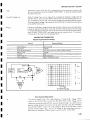
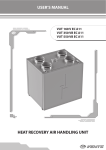
1
INSIDE FRONT COVER
CONTENTS
Section 1
S pecification
Section 2
Operating Instructions
Sectio n 3
Circuit Descri p tion
Section 4
M aintenance
Section 5
Performance Check/Cal ibratio η Proce d ure
Abbreviations and Symbols
Parts Or d ering Information
Section 6
E lectrical P arts L ist
M echanical Parts L ist Information
Section 7
Mechanical Parts L ist
Section 8
Diagrams
M echanical
P arts L ist Illustrations
Accessories
Abbreviations and symbols use d in this manual are
base d on or ta k en d irectly from IEEE Standard
260 "Stand ard Symbols for Units", MIL-STD-12B
an d other stan dards of the electronics industry.
Change infor m ation, if any, is located at the rear of
th is manual .
Fig. 1-1 . Type 576 Curve Tracer .
Type 576
Type 576
S ECTIO N 1
SPE CI F I CA ΤΙΟΝ
Change information, if any, affecting th is section will be found at the rear of the manual .
T he Ty pe 576 Curve Tracer is α dynamic semicond ucto r
tester wh ich allows d is play a nd measurement of characte ristic curves of α variety of two an d t hree terminal d evices
includ ing bi polar transistors, fiel d effect transistors, M OSFE Ts, silicon controlled rectifiers an d unij unction transistors . Α va riety of possible measurements is available using
either grounded emitter or grounded base conf ίgιι rations.
Th e instrument has available either an AC or α DC collecto r
su pp ly voltage rangi ng from 0 to ±1500 volts. The step
generator produces either current or voltage steps, wh ich
may be app lied to either the base terminal or th e emitter
terminal of the device un der test . Ste p generator outputs
range from 5 ηΑ to 2 Α in the current mo d e, an d from 5
mV to 40 V in the voltage mo d e. The step s may also be
produced as short d uration pulses . Calibrated step offset
allows offsetting the step generato r output either positive
or negative . The vertical display am p lifier measures either
collector current or leakage current with α maximum
d eflection factor of 1 ηΑ /division when making α leakage
DC Mo de
Voltages
Accuracy
R anges
R ipp le
The following electrical an d environmental characteristics are vali d fo r instruments operated at an ambient tempe ratu re of from +1 ρ °C to +40° C after an initial ωα r Μιιρ
perio d of 5 minutes, when p reviously calibrated at α temperat ιι re of +25°C ±5 °C. Section 5, P e rformance Ch eck
an d Calibration Procedure, gives α procedure for ch ecking
an d adjusting the Ty pe 576 with respect to th e following
specification .
The Ty pe 576 MOD 301W is α stan dar d Ty pe 576 wit hout the R ea dout Assembly . All t he information contained
in th is manual pertaining to th e R eadout Assem bly an d its
operation should be disregarded when used i n co nj unction
with α mo d ified instrument.
Maximum Pea k
Cu rrent ( N ormal
Mo de) ι
TABLE 1-1
ELECT RICAL CHARACT ER ISTICS
Collector Supp ly
Performan ce
C haracteristic
Sweep Modes
measurement. The horizontal d isplay am p lifier allows measurement of both collector an d base voltage.
Normal mode : AC (at line frequency) ; positive-or negative-going
full wave rectified AC .
10 Α
2Α
0 .5 Α
0 .1 Α
P ea k Current (Ste p At least At least At least At least
4Α
1 Α
Ge nerator in P ulsed
20A
0.2 Α
Steps Mode)
DC mo de: p ositive o r negative DC .
Mi nimum Series
Resistance
0.3 Ω
6.5 0
Νο -loa d : 2°/ο or less of voltage, or
0.1 % or less of fu ll range voltage.
Maximum Se ries
R esistance
65 k Ω
1 .4 ΜΩ 6.5 ΜΩ 6.5 ΜΩ
o pen circuit voltages on all
ranges within +35% and -5%.
Pea k
15 V
75 V
350 V
1500 V
I Collector Supply Maximu m Co ntinuous Peak C urrent Operating
Ti me vs Duty Cycle and Ambient Temperature. With the PEAK
POWER WATTS at 50 only, the following limitations apply: Maximum continuous operati ng time at rated current (100% duty cycle)
i nto α short ci r c uit is 20 niinutes at 25 C am bient, or 10 m inutes at
40°C a mbient. Altern atively dury cycle may be li mited to 50% at
25 °C ambient or 25% at 40°C amb ie nt. ( Α no rmal fa mily of curves
for α transistor will produ ce α du ty cycle effect to 50% or less even
if operated co nti nuously .) Over dissipation of the collector supply
will tempora rily shut it off and turn on the yellow CO LLECTOR
SUPPL Y VOLTAGE DISA BLE D light. Νο damage will result .
140 Ω
3 kΩ
Series R esistance
Available
0.3 Ω , 1 .4 Ω ,6.5 Ω ,30 Ω ,140 Ω ,
650 Ω , 3 k Ω , 14 kΩ , 65 kΩ , 300
k Ω , 1 .4 ΜΩ an d 6.5 ΜΩ , all with in
5°/ο or 0 .1 Ω .
Pea k Power W atts
Settings
0.1 W, 0.5 W, 2.2 W, 10 W, 50 W
a n d 220 W . Derived from nominal
peak op en circuit collector voltages
an d nominal series r esistance values
at n ominal li n e voltage .
Safety Inte r loc k
When MAX PEAK VO LTS switch is
set to either 75, 350 or 1500, α p rotective box must be in place over
test termi nals an d its li d closed be-
Specification-Type 576
fore voltage can be a pp lie d . Amber
light on ind icates interloc k is open ;
R e d light on in d icates voltage is being app lie d to test te rmi nals.
L oo p ing Com p ensation Cancels st ray capacitance between
collector test termi nal an d groun d
i n Stan d ard Test F ixture an d all
Standa rd Test Fixt ure Accessories .
Step Generator
4ccuracy (Cu rrent or
Voltage Ste p s, I ncl u d ng Offset)
b etween any two steps,
without .1 Χ ST EP MULT button
presse d ; within 10%ο with .1 Χ ST EP
Μ ULT bu tton p resse d .
Incremental
Accuracy
W ith in 5%
Absolute
Accu racy
W ith in 2°/ο of total outp ut, incl u d -
Step (Current or
Voltage) Am p litud es
DFF SET MU LT Control R ange
Cur rent Mode
AM PL IT U DE
Switch Range
ing any amou nt of offset, or 1°/ο of
AMPLIT U DE switch setting, whic hever is greater.
One times or 0 .1 times (with .1X
ST EP MULT b utton p resse d ) the
AM PL IT U DE switch setting.
Co ntinuously va riable from CI to 10
times AMPLITUDE switch setting,
either ai d ing or op p osing the step
ge nerator p olarity.
R ipple Plus
V oltage
M od e
AM PL IT U DE
Switch Range
Maximum Voltage
(Ste ps an d Ai d ing
Offset)
At least 10 V.
M aximum O pposingA Wh ic hever is less : 10 times AMPL I-
TUDE switch setting, or between
10 mA an d 20 mA .
Maximum Op posing Between 1 V an d 3 V.
Voltage
Offset Current
2Continuoυs DC Output vs Ti me, Temperat ure and Duty Cycle. 2Α
conti nu o us DC output can be ac hieve d fo r an un limited period up
to 30°C am bie nt. Betwee n 300C and 40°C amb ient, 2Α co ntinuo us
DC operatio n sh ould be li mited to 15 m inu tes or li mited to α 50%
duty cycle or less. Α family of steps (such as 10 steps at 200 mA per
step ) will automatically re duce the du ty cycle to 50% even if generated co nti nu ously. E xceeding the rati ng will temporarily shut off
power to the entire instrument but no damage will result.
50 mV to 2 V, in 1-2-5 seq uence.
(Steps an d Ai d i ng
Offset)
ting .
Maximum Current
(Ste p s a nd Aiding
Offset)
At least 2 Α at 10 V or less, d er ating linearly to 10 mA at 40 V.
Short Circuit Cur20 mA, 100 mA, 500 mA, +100%rent L imiti ng (Steps 0°/ο; 2 Α +50%ο-0°/ο; as selected by
an d Ai d i ng Offset) CURRENT L IM IT switch.
Maximu m Op p osing 10 times AMPL IT U DE switch setOffset V oltage
i ng.
Maximu m O pp osing L imited betwee n 10 mA an d 20
Current
mA
R i pp le P lus
N oise
0.5%ο or less of AM PL IT U DE switch
setting, or 2 mV, p ea k to peak.
Step R ates
( Fr ont p anel R AT E button labels in
pa rentheses.) 1 times ( .5Χ ), 2 times
(N O R M ) an d 4 times (2 Χ ) line freq uency . Steps occu r at zero collector voltage when .5 Χ or N O R M
RAT E buttons are p resse d , and also
at peak voltage when 2Χ R AT E
button is p resse d . Ste p s occur at
collector voltage p eak an d at
normal r ate when .5 Χ and 2Χ.
RAT E buttons are p resse d together .
P ulsed Ste ps
Pu lsed ste p s 80 μs or 300 μs wi d e
within +20°/ο , -5°/ο p ro d uce d wh enever one of the PULS E D ST EP S
buttons is p ressed . P ulse d ste p s can
be p rod u ce d only at normal an d .5
times normal rates. Collector
Supply mode automatically becomes DC when either the 300 μs
or 80 μs PULS E D ST EP S button is
p ressed unless P OLAR ITY switch is
set to AC . If the 300 μs and 80 μs
PULSED STEP S buttons are p resse d together, 300 μs pulsed steps are
p ro d uced , but collecto r su pp ly
mo de does not change .
200 mA to 50 ηΑ , in 1-2-5 sequence .
ting, exce p t 10 times switch setting
when switch is set to 200 mA, an d
15 times switch setting when t h e
switch is set to 100 mA .
0.5%ο or less of AMPLIT U DE switch
setting or 4 ηΑ , pea k to peak.
M axim u m Voltage 20 times AMPLIT U DE switch set-
M aximum Cu rrent 20 times AMPLIT U DE switch set(Ste p s an d Ai d ing
Offset ) 2
N oise
S pecificatio n -Type 576
Step s an d Offset
Correspon ds with collector sup p ly
pola rity (positive going when POLAR ΙΤΥ switch is set to AC) when
th e P OLAR ITY I NVER T button is
release d . Is o pposite collector su p p ly pola r ity (negative-going in AC)
when eith er t he POLARITY INVERT button is p ressed or t h e
L ead Selector switch is set to BAS E
G R O UN D E D. If L ead Selector
switch is set to BAS E G ROUN DE D, P OLAR ITY I NVER T button
h as no effect on steps an d offset
polarity .
Polarity
Step Families
R e petitive families of characteristic
curves generated wit h REP ST EP
FAMILY button presse d . Single
family of c haracteristic curves generated eac h time SI N G LE ST EP
FAM I L Y b utton is p ressed .
N umber of Ste ps
R anges from 1 to 10 as selected by
the NUMBER OF ST EP S switch.
For zero ste ps, press SI N G LE ST EP
FAM Ι L Y bu tton .
Display Am plifiers
Disp lay Accuracies
(οι'οο f H ig hest OnSc reen Value)
Dis p lay magnified (DISPL AY O FF SET Selecfor switch set to either
VERT Χ 10 or HO R IZ
X10) and offset between
100 an d 35 an d 10 an d
40 divi- 15 d ivi- 0 d iviions
sions
sions
E xternal
H ori-
zontal (T hroug h
I nte rface)
Leakage
Su pp ly
2ο/ο
3ο/ο
Vertical E mitter
Cu rrent (VER TICAL Switch set
between 10 ηΑ
an d 2 mA)
Vertical Emitter
Current (VER TICAL Switch
set to 5 ηΑ , 2
ηΑ or 1 ηΑ )
2ο/ο ±1
ηΑ
3ο/ο ±1
ηΑ
4%
3ο/ο
E xternal Ve rt-
2%ο
3%ο
4%ο
3%
H orizontal Collector V olts
2%ο
3ο/ο
4%ο
3ο/ο
2%
3%ο
4%ο
3%
ical (Through
Ιnterface)
H orizontal B ase
V olts
3ο/ο ±1
ηΑ
5ο/ο ±1 ηΑ
Not A pp licable
Η ο r ί z οη tαΙ
Collecto r or
Base Volts
VER TICA L
switch set to :
1 μΑ o r mo re
2%ο
3ο/ο
4ο/ο
3ο/ο
100 ηΑ , 10
πΑ or 1 ηΑ
N ot App licable
3%ο plus
0 .025 V
fo r each
vertical
d ivision of
deflection
ο η the
C RT
500 ηΑ , 50
ηΑ or 5 ηΑ
N ot App licable
3%ο plus
0.125 V
for each
vertical
d ivision of
d eflection
ο π t he
CRT
200 ηΑ , 20
ηΑ or 2 ηΑ
Not App licable
3%ο plus
0 .050 V
for each
vertical
d ivision of
d eflection
of t h e
Collecto r Su pp ly
Mo d es
3%
4ο/ο ±1
ηΑ
Collecto r
N ormal an d DC
2%ο
3ο/ο
M ode
Disp lay
Unmagnified
Vertical Collector Cu rrent
4ο/ο
CRT
Ste p Generator
Display
Specificatio n-Type 576
Vertical Ste p
Generator
3ο/ο
4ο/ο
5ο/ο
4ο/ο
H orizontal Step
3ο/ο
4ο/ο
5ο/ο
4ο/ο
Generator
Deflection Factors
Vertical
Collector Current
1 μΑ/division to 2 Α/d ivision in
1-2-5 se q uence.
E mitter Current
1 ηΑ/d ivision to 2 mA/d ivision in
1-2-5 se q uence.
Ste p Generator
1 ste p /d ivision.
H orizontal
Collector Volts
Base Volts
50 mV/division to 2 V/d ivision in
1 2 5 se q uence.
ance
At least 100 ΜΩ wit h
H O R IZONTA L switc h set to 50 mV, 100 m V
an d 200 m V BAS E ; 1 ΜΩ wit h in
2 ο/ο wit h switch set to .5 V, 1 V and
2
Step Generato r
M aximum
N oise
H orizo ntal
CO LLECTO R
BAS E
Calibration Chec k
Display Positioning
Accuracy U sing
PO L A R ITY Switch
S p ot p ositioning with change in
P OLAR ITY switch setting (usi ng
AC position as reference), within
0.1 d ivision of :
1 ste p / d ivision
Centere d
-5 d ivisions
+5 d ivisio ns
AC
+( ΝΡΝ )
-( ΡΝΡ )
CRT
Ty p e
E lectrostatic
Screen Size
Calibrate d area
1 Α
1 ηΑ
1 μΑ
1 ηΑ
10
d ivisions;
h orizontally
Ty p ical
tial
75
Ce nte red
-5 d ivisions
+5 d ivisions
CRT an d Rea d out
lerating
15
H orizontally
deflectio n .
of
12
(1
10
d ivisions
u sable
d ivision
by
divisions
e q uals
1
cm) .
1 ο/ο or less, or
MAX PEAK VO LTS Switch
CO LLECTO R
E M ITTER
Vertical or H orizontal offset of d isp lay centerline value up to 10 d ivisio ns in 21 half d ivision steps.
V.
Disp laye d
Vertical
Disp lay Offset
Vertically
50 mV/d ivisio n to 200 V/divisio n
in 1-2-5 se q uence
In p ut Im p ed-
Vertical an d Ηο rίzCoarse p ositioni ng in 5 d ivision inontal P osition Control crements within 0 .1 d ivision; co ntinuous fine p ositioning over at
least 5 d ivisions for each coarse position.
350
1500
2 μΑ
2 ηΑ
5 μΑ
5 ηΑ
Accel-
Poten-
R ea d o u ts
4000
V
Automatic
d igitally
lig
h ted
dis p lay .
R ea d out is automatically blan ked if
read ings woul d be outside t he avail-
able ranges or would give er roneous
d is p lay.
PER VERT DI V
5 mV
5 mV
20 mV 200 mV
5 mV
5 mV
5 mv
5 mV
With DISPL AY O FF SET Selector
switch set to N O RM (O FF ), s p ot is
deflected 10 d ivisions both vertically an d h orizontally withi n 1 .5ο/ο
whenever the CA L button is pressed .
1 ηΑ to 20 Α calculated from VERTICA L switch setting, DISPL AY
OFFSET Selector switch setting
and M OD E switch setting (o r Χ 10
Vertical Interface I n p ut) .
PER HO R IZ DI V
5 mV to 200 V calc ulate d from
setting an d
H OR IZO N TA L switch
E
DISPL AY O FF S T Selector switch
setting
W ith DISPLAY O FF SET Selector
PER ST EP S
5 ηΑ to 2Α a n d 5 mV to 20 V calculated from AMPLIT U DE switch
setting and .1 Χ ST EP MULT b utton position (or
X10 Ste p I n terface
In p ut) .
switch set to Χ10 M AG N I FI ER
(either axis) th e calibration s p ot is
within 0.5ο/ο of ze ro spot ( p revious
Ιγ set to CRT graticule cente r)
when CA L button is p ressed .
Specification-Type 576
βο rg m PER DI V
1 μ to 500 k calculated from VERTICA L switch setting, DISPL AY
O FF SET Selector switch setting,
AMPL IT U DE switch setting, .1X
ST EP MULT button p osition, Χ10
Vertical Interface In put an d Χ10
Step Interface In put .
Th is instrument is d esigned for
operation from p owe r source wit h
its neutral at or near ground (earth )
potential . It is not intend e d fo r
o p eration from two phases of
multi- phase system, or across legs
of single-phase, three wi re system .
It is p rovided with α th ree-wire
powe r cord with three-terminal
polarized plug for connection to
the power source . Thir d wire is
di rectly connected to instrument
frame, an d is intended to ground
th e inst rument to protect operating
p ersonnel, as recommen ded by
national an d inte rnational safety
co des .
L ine Voltage
R anges
Low
Medium
H ig h
115 VAC
230 VAC
90 V to 110 V
104 V to 126 V
112 V to 136 V
180 V to 220 V
208 V to 252 V
224 V to 272 V
Line Fre quency R ange 48 to 66 H z
M axim um Power
Consum ption at 115
VAC, 60 H z
Temperature
N onoperating
N onoperating
To 50,000 feet
Operating
To 10,000 feet
Operating
15 minutes along each axis at 0.015
inch with freque ncy varied from
10-50-10 c/s in 1-minute cycles.
Th ree minutes at any resonant
point or at 50 c/s.
S hoc k
Nonoperating
Transportation
30 g's, 1/2 si ne, 11 ms d uration, 1
shoc k p er axis . Total of 6 shoc ks
12 inch p ac kage d rop. Qualified under the N ational Safe Tra nsit Committee test p rocedure 1 Α.
TABLE 1-3
ME CHANICA L CHARACT ER ISTICS
Descri ption
Characteristic
Dimensions
Height
W idth
De pth
-15 inches
-11 3/4 inches
-23 1/4 inches
-69 lbs.
Finis h
Table 1-2
ENVI RONMEN TA L CHARACTER ISTICS
C haracteristic
Altitu de
W eight
305 W, 3.2 Α
0 ° C to +50 ° C
Specified Op eration +10 °C to +40 ° C
Vibration
Power Requireme nts
Power Connection
U seful Op eration
Information
-400 C to +65° C
Front Panel (Type
576 an d Stan d ar d
Test F ixture)
Cabi net
Trim and R ear
Panel
Anodized Aluminum
lue vi nyl painted aluminum
Oatin finished chr ome
This page intentionally blank.
S E CTIO N
Ty pe 576
2
OPER A TI N G INST RU CTIO NS
Change info rmation, if any, affecti ng th is section will b e found at the rear of the ma nual .
General
T h is section of the instruction manual p rovi des information necessary for operating the Ty pe 576 and for using it
to test va rious semico nd uctor d evices . Included are setup
proced ures, α d escription of th e Type 576 controls and
connectors, α d iscussion of th e theory of the inst rument, α
first time operation p roce dure, and general operating info rmation . Also i ncluded is α section d escribing the use of the
Ty pe 576 for measu r ing the characte ristics of various semiconducto r d evices .
Cooling
I N ITIA L
VO LTAGE S ELECTO R assembly, must be set to the position wh ich correspon ds to the line frequency being u se d .
Use the following p rocedure to convert this instrument
between line voltages, regulating ranges or line frequencies :
1 . Discon nect the instrument from the p ower source .
TABLE 2-1
R egulati ng R anges
CONSID ER ATIO NS
The Ty pe 576 maintains α safe operating temperature
when operated in an ambient temperature of 0 ° C (122 °
F) . Adequate clearance on all si des of the instrume nt
shoul d be provided to assure free air flow and d issi patio n of
h eat away from the instrument . Α thermal cutout in the
instrument p rovides thermal p rotection by d isconnecting
the p ower to th e i nstrument if the internal temperatur e
exceeds α safe operating level. Power is automatically
restored when th e temp eratu re ret urns to α safe level . It
should be noted that the instrument will turn off un der
ce rtain conditions of h ig h collector su pp ly current output
or h ig h step gene rator cu rrent Output even though the
inst rume nt is being operated in an ambient temp erature
wh ich is with in the specifie d r ange . See footnotes in th e
Specification section for furt her info r mation .
R ange Selecto r
Switch Positio n
L O (switc h bar in
left h oles)
Μ (switc h ba r in
mi dd le h oles)
Η Ι (switc h bar i n
right holes)
R egu lati ng R ange
230 V olts
115 V olts
N omi nal
_
Nominal
180
to
220
volts
90 to 110 volts
104 to 126 volts
208 to 252 volts
112 to 136 volts
224 to 272 volts
Operating V oltage and F requency
The Ty pe 576 ca n be operated from eit h er α 115-volt or
α 230-volt line voltage source . The L I NE VOLTAG E S ELE CTO R assembly, locate d on the rear panel, allows co nversion of the instrument so that it may be operated from
one line voltage or the other . In add ition, this assembly
changes the connections of the p ower transformer p rima ry
to allow selection of one of three regulating ranges (see
Table 2-1) . The assembly also includes the two line fuses.
Wh en the instrument is converted from 115-volt to 230-volt
operatio n or vice versa, the assembly selects the p ro per fuse
to provide the correct p rotection for the instrument.
Th e Ty pe 576 may be operated from either α 50 H z or α
60 H z line f requency . In order to sync hronize t he step
ge nerator with the collector su pply, the 60 H z-50 H z
switch , located on the Ty pe 576 rea r p anel below the L I NE
Fig . 2-1 . Line Voltage Selector assembly and 60 Hz-50 Hz switch
on the rear panel (shown with cover removed) .
Operating Instructions-Type 576
Fig. 2-2. Front-panel controls, connectors and readout.
2-2
O per ati n g
I
n structions-Type
576
2 . L oosen th e two captive screws w h ic h h ol d th e cover
onto t he voltage selector assembly, t h en pull to remove the
cover.
3. To convert from 115-volt to 230-volt line voltage or
vice versa, pull out the V oltage Selector switch bar (see F ig .
2-1) ; turn it 180° an d pl ug it back i nto the remaining h oles .
Change the line-cor d power plug to matc h t he power-source
rece ptacle or use α 115-to-230-volt adapter.
4. To change regulating ranges, pull out the R ange Selector switch bar (see F ig . 2-1) slid e it to the desired position an d plug it back in . Select α range whic h is centered
about the average line voltage to wh ich t he instrument is to
be connected (see Table 2-1 ) .
5. R e-install the cover an d tighten the two ca ptive
screws.
6. To convert from operation with 60 H z line freq uency
to operation with 50 H z line frequency (or vice versa), slide
the 60 H z-50 H z switch (see Fig. 2-1) to the position wh ic h
coinci des with t he line freq uency being used.
7. Before applying power to the i nstrument, chec k t hat
the in d icating tabs on th e switch bars are p rotru ding
throug h t he correct holes in the voltage selector assembly
cover for th e desired li ne voltage an d regulating range.
CA UTIO N
The Ty pe 576 should not be operated with t he V oltage Selector switch or the R ange Selector switch in
t he wrong position for the line voltage app lied .
Operation of the instrument with either of these
switches in t he wrong p osition will cause incorrect
operation and may damage t h e instrument .
CO NTROLS, CO NNECTORS AN D RE ADOUT
All controls an d connectors r equire d for normal operation of the Type 576 are locate d on the front an d rear
panels of t h e instrument an d on the front panel of the
stan dard test fixture (see F igs. 2-2 an d 2-3) . In add ition,
readout of some of the instrument functio ns has been provi ded on the front panel . F amiliarity with the functio n an d
use of each of these controls, connectors an d t he readout is
necessary for ef fective operation of the instru ment . The
functions are described in the following table.
Controls
C RT an d R ea dout
I NTEN SITY
Control
Controls brig htness of d is play.
F OC US
Control
Provides adjustment for optimum d isplay definition .
RE ADOUT
Co n trols brig h tness of readout .
Fig. 2-3. Rear-panel controls.
Ι LLUM
Control
SCA LE I LLUM
Control
Connector
CAMERA
PO WER
Connector
Controls graticule illumination .
Provides +15 volts for operation of
came ra.
R eadouts
PER VERT
DI V R ead out
Readout in d icates deflection factor of
vertical d is play as viewed on C RT.
PER H OR IZ
DI V Reado ut
R ea dout indicates
PER ST EP
R ea d ou t
R ea dout in dicates am p litu d e p er step
of Ste p Generator output .
β OR gm
PER DI V
R ea dout
R ea dout in dicates beta or transconductance per division of C RT display,
d eflection factor of
h orizontal d isp lay as viewe d on C R T.
Display Se nsitivity and P ositioning
VER TICA L
CURREN T/DI V
Switch
Selects vertical deflection factor of display.
COLLECTOR-Normal operation
of i nstrument . V ertical d is play re presents collector current . U se blac k
units to d etermine vertical deflection factor .
2-3
O perating Instru ctions-Type 576
EMITTER-Operation of instrument with MOD E switch set to
LE A K AG E ( E M ITT ER C URRENT) . Vertical d isp lay rep rese nts
emitte r current. U se orange units to
determine vertical d eflection factor.
STEP G EN-Ste ps in d icating Step
Generator output are disp layed
vertically . AMPLIT U D E switch setting per d ivision determines ve rtical
deflection factor .
DISPL AY O FF S E T Allows selection of d isp lay offset or
Selector Switch
display offset an d magnification .
N OR M (O FF )-Dis p lay offset is not
operable .
H OR IZ Χ 1-Allows h orizontal d isplay to be offset u sing calibrate d
C EN TERL I NE VALUE switch .
VERT Χ1-Allows; vertical d is p lay
to be offset u sing calibrated C ENTERLI NE VALUE switch .
Η Ο R Ι Ζ X10-Horizontal dis p lay
magnified by 10 times. Allows h orizontal d isplay to be offset using
calibrated CEN TERLINE VALUE
switch.
VER T X10-Vertical d is p lay magnified by 10 times. Allows ve rtical
disp lay to be offset using calibrate d
C EN TERL I-NE VALUE switch .
C EN TERL IN E
VA LUE Switch
HO R IZO NTA L
VO LTS/DI V
Switch
2-4
(Clear p lastic flange with numbers on
it) P rovi d es calibrated offset of display .
Χ 1 (VER T or H OR IZ)-Number οη
C EN T ERL I NE VA LUE switch
a pp ea ring in bl u e win d ow r e p resents number of divisions centerline
of d isp lay is offset eith er vertically
or horizontally from zero offset
li ne.
Χ 10 (VER T or HO R IZ)- N umber
on CEN TERLI NE VALUE switch
a pp eari ng in bl ue window multip lie d by 10 represents num ber of
d ivisio ns ce nterline of d is p lay is offset either vertically or horizontally
from zero offset line .
Selects the horizontal d eflectio n factor
of d is p lay.
CO LLECTO R -Horizontal d is p lay
re p rese n ts collector voltage to
grou nd .
B AS E -Horizontal d isp lay rep resents b ase voltage to ground .
ST EP G EN -Steps in d icating Step
Gene rator out p ut are d isp layed
h orizontally. AMPLITU DE switch
setting per d ivisio n dete rmi nes h ori-
zo ntal deflectio n factor .
Z ER O Button
Pr ovi des α ze ro reference for the d isp lay.
N ORM-When DISPL AY O FF SET
selector switch is set to N ORM
(OFF), ZERO button p rovi d es
point on C RT of ze ro vertical an d
h orizontal deflection for adjusting
positio n controls .
DIS PL AY OFFSET-When DISPL AY OFF SET Selector switch is
in one of fo ur d is p lay offset p ositions, ZER O button p rovi d es reference point on CRT whic h must
be positione d to vertical ce nte rline
(horizontal offset) or to horizontal
centerli ne (vertical offset) to insure
that t he CEN TERL I NE VALUE
switch setting a pp lies to ce nte rline .
(Shoul d always be chec ke d with
DISPLAY OFF S ET Selector switch
is set to M AG N I F I ER .)
CA L Bu tton
P rovi d es signal wh ich shou ld cause 10
d ivisions of vertical and h orizontal d eflection for chec k ing calibratio n of
ve rtical an d h orizontal am p lifiers.
N O R M -Whe n DISPL AY OFFSET
selector switch is set to N O RM
(O FF ), CA L button provi d es p oint
on C R T of 10 d ivisions of vertical
and h orizontal d eflection.
DIS PL AY O FF S ET-W hen DISPL AY OFFSET Selector switch is
in one of four dis p lay offset p ositions, CA L button provides signal
whic h s h oul d cause reference poi nt
on C RT to a pp ear on vertical centerline ( h orizontal offset) or on
h orizontal centerline (vertical offset), assuming zero reference point
was p ro p erly a d ju sted . (C hec k
shoul d be perfo rmed with DISPL AY O FF S ET Selector switch set
to MAG N I F I ER .)
DISPLAY INVER T Inverts d is p lay vertically an d h orizonButton
tally about center of C R T.
P OSITIO N Switch
(Horizontal)
Provi des coarse positio ning of h orizontal d is p lay.
F I NE POSITIO N
Control
( Horizontal)
d is p lay.
Provi d es fine p ositioning of horizontal
POSITIO N Switch
( Vertical)
Provi d es fi ne p ositioni ng of ve rtical
d isp lay .
O perating I nstru ctions-Type 576
F I NE POSITIO N
Cont rol (Vertical)
Controls
MAX PEAK
VOLTS Switch
PEAK P OWER
WATTS Switch
Provides fine p ositioning of vertical
disp lay .
LE A K AG E (EM ITT ER C URRENT)-Ve rtical sensitivity is increased 1000 times. Vertical amplifie r measures emitter current. Collector Sup p ly mode set for DC voltage outpu t.
Collecto r Supp ly
Selects r ange of VA R IA BLE CO LLECTO R S UPPL Y control . Switch is locate d below PEAK P OWER WATTS
switch and ra nge is in d icated by wh ite
arr ow . When switch is set to 75, 350
and 1500, protective box must be used
with Stan d ard Test F ixt u res (see section on inte rlock system) .
Selects nominal pea k power out put of
Collecto r S u pp ly, by selecting r esista nce in series wit h Col lector S upply
out p ut . PEAK P OWER WATTS is
in d icated by number on transparent
switch flange a ppeari ng above white
MAX PEAK V O LTS in d icator .
SER I ES RE SISTO RS are indicate d by
b lac k i n d icato r. PEAK POWER
WATTS switch must be pulled out to
set nominal pea k power outp ut. Wh en
PEAK P OWER WATTS switch is set,
se r ies r esistance is automatically
change d to mai ntain desired nominal
pea k power out p ut when MAX PEAK
V O LTS switch setting is change d .
L OO PI N G
CO MPENSATIO N
Control
Allows ad justment of looping compensation . Allows compensation of internal a nd a d apter st ray capacitance .
Does not compensate for d evice capacita nce .
CO L L ECTOR
S UPPLY RESET
Bu tton
Resets Collector Su pp ly if it h as been
d isabled by internal ci rcu it brea ker.
Collector S upply is turned off whenever maximum current rating of transformer primary of 1 .2 Ampe r es is exceeded .
POWER ON-OFF
Controls inp ut power to i nst ru ment.
Switch
L ights
POW ER L ig ht
L ights wh en p ower is on .
CO LLECTOR
S UPPLY VO LTAG E DISA BLE D
L ig ht
Ind icates Collector Su pp ly voltage h as
been disabled . L igh ts when Collector
Su p ply may present α pote ntially
dangerous voltage at its output . In
such α case, use of protective b ox is
re q ui red to enable Collecto r Supply .
Also ligh ts when h ig h cur rent generated by Collector S u pply or Ste p
Generator causes inst rument to overheat.
VAR IA BLE CO L- Allows varying of collector supply
LECTO R S UPPL Y voltage within range set by MAX
Control
PEAK VOLTS switch .
P O LA R ITY Switch Selects pola rity of Collector Sup p ly
Controls
voltage an d Step Generator out p ut .
NUMBER O F
-( ΡΝΡ)-Collector Su p p ly voltage
Ste
ST EPS Switch
an d Step Generato r out p ut a re
negative-going .
+( ΝΡΝ )-Collector Su pp ly voltage
and Step Generator outp ut are
p ositive-going.
AC-Collector Su pp ly voltage is
both positive- and negative-going
(sine wave); Step Generator output
is positive-going . Wh en switch is set
C URRENT
P rovides
current limit of the Step Gen-
erator out p ut when voltage ste p s are
being prod uced .
ST EP /O FF S ET
Selects am p lit ude per step of steps and
offset of Ste p Generator out p ut .
AMPLIT U DE
Switch
to AC position , use .5 Χ step r ate
Selects mode of o p eratio n of Collecto r
Su pp ly .
N ORM -Normal Collector Supply
outp ut is obtained .
DC (ANTI LOOP)-Collector Supply output is DC voltage eq ual to
pea k value set by VAR IA BLE CO LLE CTO R S UPPL Y control .
Selects number of steps p er family of
p Gene rator out put.
L I M IT Switch
Am p litu d es with in blac k arc re p resent
cu rr ent steps; with in yellow arc, volt-
age ste p s . N ote cautio n on front- p anel
when usi ng voltage steps.
an d normal mo d e of operation.
M OD E Switch
Step Gene rator
O FF S E T
Buttons
Allows offsetting of Step Generato r
out p ut using OFF SET M UL T co ntrol .
ZERO-No offset available.
AID-Allows ze ro ste p of Ste p Generator out p ut to be o ffset as many
as 10 ste p s above its ze ro offset
level.
2-5
O perating Instructions-Type 576
OPP OS E-Allows zero step of Ste p
Generator out p ut to be offset as
many as 10 ste p s below its zero offset level .
O FF S E T M ULT
Cont rol
ST EP S Button
Provi d es calibrated offset of step Generator out p ut to ±10 times AM PL ITUDE setting when eith er OFFSET
AID or OFF S E T OPPOS E button is
pressed.
ST EP /O FF S ET
POLAR ITY INVERT Button
Allows c hange of p olarity of Step Generator outp ut (from polarity set by
P OLAR ITY switch) .
ST EP MULT .1 Χ
B utton
Provides 0 .1 times multiplication of
ste p am p litu d e, but does not effect
offset .
P rovides ste p s of normal d uration
(step lasts for entire p eriod of rate
cycle) .
PULSE D ST EPS
Buttons
Allows Ste p Generator out p ut to be
a pp lied to Device U nder Test for only
α portion of normal ste p d uration .
Pu lsed ste p s occu r at pea k of Collector
Sup p ly out put.
300 μs-Selects pulsed ste p s with
d uration of 300 μs. Collecto r Supply is automatically switched to DC
mo de.
80 μs-Selects pulse d steps with
d uration of 80 μs. Collector Sup p ly
ίs a u tomatically switched to DC
mode.
300 μs an d 80 μs-Wh en buttons
are p resse d together, selects pu lsed
ste p s with d uration of 300 μs; h owever, Collector Su pp ly is not automatically switched to DC mo d e.
STEP FAM I LY
Bu ttons
Allows ste p s to be gene rated in re p etitive families or one family at α time .
ON REP-Provi d es re p etitive Ste p
Generato r out p ut .
OFF SI N G LE -Provi d es one family
of steps wh e n ever button is pressed .
Once button has been presse d , Ste p
Gene rator is turne d off until
presse d again or until ON REP button is pressed.
RAT E Buttons
Selects rate at whic h ste ps are gene rate d .
N O R M -Provi d es normal Ste p Generator rate of 1 Χ normal Collector
Su pp ly rate (120 ste p s p er secon d
for 60 H z line freq uency) .
2X-Provides rate of two times normal rate .
.5X-Provides rate of one h alf normal rate.
2Χ an d .5X-Wh en buttons are
p ressed together, p rovi des normal
rate but with ste p transistions occuring at p ea k of Collector Su pp ly
swee p .
2-6
2Χ and .5X-Provides normal rate
but with ste p transitions occurring
at p ea k of Collector Su pp ly swee p .
Controls
Stan d ard Test F ixture
Selects way in wh ich Ste p Generator is
a pp lied to Device U nder Test . In all
positions Collector Su pp ly output is
connected to Collector terminal .
EMITTER G ROUN DED- E mitter
of Device U n d er Test is connected
to groun d .
ST EP G EN -Ste p Generator is
ap p lied to base te rminal of
Device U n d er Test . N ormal operating p osition .
OPEN (O R ΕΧΤ)- Base te rminal
of Device U nder Test open . External signal a pp lied to ΕΧΤ
BAS E O R EMIT INPUT connector, will be ap p lied to base termi nal .
SH O RT- Base terminal of Device U n d er Test is s h orted to
emitter terminal .
BAS E G R OUN DE D- Base terminal
of Device U n der Test is connecte d
to ground . Step Generator polarity
is inverted .
OPEN (O R ΕΧΤ)- E mitter terminal of Device Un d er Test is
open . E xternal signal a pplie d to
ΕΧΤ BAS E OR EMIT INPUT
co nnector, will be a pp lied to
emitter terminal .
STEP G EN -I nverted Ste p Generator outp u t is a pp lie d to emitter of Device U n der Test .
LEFT-O FF-R IG H T Selects whic h device (c hoice of 2) is to
Switch
be teste d , left or rig ht.
Te rminal Selector
Switch
Inte rlock
Switch
Connectors
Ad a p ter
Connectors
E nables Collector Su pp ly when Protective Box is in place an d li d is closed .
Allows connection of various test
a d a p te rs to Stan d ar d Test F ixture .
Connecto rs will acce p t stan d ar d size
Operating Instructions--Type 576
ST EP G EN OU T
Connector
ΕΧΤ BASE O R
EMIT INPUT
Connector
G R O UN D
Connector
Allows in put of externally generate d
signal to eith er base terminal or emitter terminal of Device Under Test as
determined by Terminal Selector
Switch .
P rovi des external access to ground reference .
L ight
Caution L ig ht
R ed light on, indicates Collector Su p-
ply is enabled an d dangerous voltage
may app ear at collector terminals.
Controls
Line Voltage
Selector Switches
60 H z-50 H z
Switch
banana plugs if some ot her means of
connecting Device Un der Test to
Stan dar d Test Fixture is d esired . C, Β
an d Ε stan d for collector, base and
emitter, respectively . Unlabeled terminals allow K elvin sensing of voltage for
h ig h current devices.
Ste p Ge nerator output signal appears
at t h is connecto r.
I ndicates controls and statements associated with the voltage mo de of operation of the Step Generator.
Yellow
Blac k ( B uttons)
In dicates function controlled by α
si ngle button, wh ic h is released for
most common app lications.
Dark Grey
( B uttons)
In dicates function controlled by seve rαΙ buttons, an d t he d ar k grey button is
p ressed for most common app lications.
PRECA U TIONS
Α number of t he Ty pe 576 front- panel controls coul d,
th rough im p ro p er use, cause damage to t he device un d er
test . Fig . 2-4 indicates the area of the Ty pe 576 front panel
where these co ntrols are locate d. Care shoul d be exercise d
when using controls located in this area .
R ear Panel
selects
Switch
assembly
operating voltage an d line voltage range.
Also includes line fuses.
Voltage Selector-Selects ope rating
voltage (115 V or 230 V) .
R ange Selector-Selects line voltage
range (low, me dium, high).
Allows conve rsion of inst rument
for o peration with either 60 Hz
or 50 Η 7 line frequency .
FR ONT PANEL CO LO RS
T he various colors on the front-panel of the Ty pe 576
an d Stan dard Test Fixture in d icate relationsh i ps between
controls and control functions. Table 2-2 shows t he relationshi p w hic h each color in dicates .
Table 2-2
Colors and Controls
Color
R elationship
Green
In d icates controls wh ich affect the
Step Generator polarity.
Bl ue
In d icates controls an d statements associated with d isplay offset .
Orange
In dicates relationship of LE A KAG E
(EM ITTER CURREN T) mo de with
t he VER TICA L a nd HO R IZON TA L
switches .
Fig. 2-4. Co ntrols located in light area of Type 576 front- panel
co uld cause damage to α device under test if used im pr operly.
G ENER A L
D ESC R IPTIO N O F IN ST RU MEN T
OPERATIO N
T he Ty pe 576 is α semiconductor tester whic h d is plays
an d allows measurement of both static an d dynamic semiconductor characteristics obtained un der simulated o perating conditions . The Collector Su pply an d the Step Generator p roduces voltages an d currents whic h are app lied to the
device un der test . The d is play am plifiers measure the
effects of these app lied conditions on the device under test .
2- 7
O perati ng Instructions-Ty pe 576
Horizontal
Deflection P lates
V ertical
Deflection
Plates
Fig . 2-5. Basic Block diagram showing ty pical connect ions o f Collector Supply, Step Generator and Display Am plifiers to the device under
test.
T he r esult is families of characteristics curves traced on α
C RT.
The Collector Supply circuit normally p ro duces α fullwave r ectified sine wave whic h may be either positive- or
negative going. The am plitu de of the signal can be varied
from 0 to 1500 volts as determine d by the MAX PEAK
VO LTS switch and t he VA R IA BLE CO LLECTO R S UPPL Y
control . Th is Collector S u pp ly outp ut is applied to the collector (or equivalent) terminal of the d evice ιι nde r test .
The Step Generator prod uces ascending steps of current
or voltage at α normal rate of one step per cycle of the
Collector Su pp ly . The amount of current or voltage p er
step is controlled by the AMPL IT U DE switch an d t he total
number of steps is cont rolled by th e NUMBER OF ST EPS
switch . This Step Generator o u tp u t may be applie d to
either th e base or the emitter (o r e quivalent) terminals of
the d evice un der test .
The d is play am p lifiers are connected to t he d evice un der
test . Th ese am plifiers meas u re t he effects of t he Collector
Su pp ly an d of the Step Generator on the d evice un der test,
am p lify th e measu rements and apply th e resulting voltages
to the d eflectio n p lates of the CRT. The se nsitivities of
these am p lifiers are controlle d by the VER TICA L C URREN T/DI V switch an d t he H ORIZO NTA L VOLTS/DI V
switch.
Fig. 2-5 is α bloc k d iagram showing th e connection of
1
these ci rcuits
to the device un der test for α ty pical measurement .
2-8
F I RST TIME O PERATIO N
When the Ty pe 576 is received, it is calibrated an d
s hould be p erforming within the specification shown in Section 1 . The following p roce dure allows the operator to become familiar with t h e front panel controls an d their fu nctions as well as how they may be used to d isplay transistor
or diod e c h aracte ristics . T h is p roce dure may also be used as
α ge neral chec k of the instru ment's perfo rmance. For α
chec k of the instrument's operation with respect to the
specification given in Section 1, the P erformance Chec k an d
Calibration Procedure in Section 5 must be used .
1 . App ly powe r to th e Ty pe 576.
2. Allow the instru ment to warm up for α few minutes.
Instrument should o perate with in specified tolerances 5
minutes after it h as been tu rne d on .
3. Set the Ty p e 576 an d Stan dard Test Fixture frontpanel controls as follows :
RE ADOUT Ι LLUM
Fully countercloc kwise
G RATIC ULE Ι LLUM
Fully counterclockwise
I NTEN SITY
Fu lly co untercloc kwise
FOCUS
Centered
VER TICA L
mA
Operating Instru ctions-Ty p e 576
DIS PL AY O FF S E T
Selecto r
N O RM
C EN TERL I NE VA LUE
0
(O FF )
H O R1
IZONTA L
V CO LLECTO R
Centere
Vertical P OSITIO N
d
Vertical F I NE P OSITIO N Centered
Ce
H orizontal POSITIO N
ntered
CR T
an d
R ea d out
Controls
4. Turn the G RATIC U LE Ι LLUM control t hroug hout its
range. N ote that the gratic u le lines become illu minate d as
the co ntrol is turned cloc kwise . Set the control for desire d
illumination .
5. Tu rn the RE ADOU T Ι LLUM co ntrol throug hout its
range. N ote that the fiber-optic rea d outs an d t he read out
titles become illuminate d as the control is turned cloc kwise .
Set the control for the desired readout illumination . The
rea d out shoul d rea d fo r these initial control settings; 1 mA
per vertical divisio n , 1 V per horizontal division, 50 ηΑ per
ste p an d 20 k β or gm per d ivision .
H orizontal
F I NE P OSITIO N
Centere d
ZERO
R eleased
CA L
Released
DISPL AY I NVER T
Released
7. Turn the F OC US co ntrol throug hout its range. Ad ju st the F OC US control for α sharp , well-defined sp ot .
ΜΑΧ PEAK V OLTS
15
Positioning Controls
PEAK POWER WATTS
0.1
VAR IA BLE CO LLEC-
F ully Co untercloc kwise
POLARITY
AC
M OD E
NO RM
L OO PI N G
As is
NUMBER OF ST EPS
1
CURRENT L I M IT
20 mA
AMPLIT U DE
0.5 μΑ
O FF S ET
Z ER O
ST EPS
Presse d
PULS E D ST EP S
R eleased
TO R SUPPLY
CO MPEN SATIO N
REP
ST EP F AM I LY
ON
R AT E
NO R M
POLAR ITY I NVER T
R elease d
ST EP MULT .1 Χ
R elease d
Terminal Selector
B AS E TER M
ST EP G EN
LEFT-OFF-R IG HT
OFF
6. Tu rn t he I N TEN SITY control cloc kwise until α sp ot
a ppears at the center of the CRT g raticule. To avoi d burning the CR T phosp h or, a dju st the I NTEN SITY control until
the s p ot is easily visible, but n ot overly brig h t.
8. Turn the ve rtical F I NE P OSITIO N control throug hout its range. N ote that the cont rol h as α ra nge of at least
-1-2.5 d ivisions about the center horizontal li n e. Set the co ntrol so that the s p ot is centered vertically on the CRT graticule .
9. Re p eat ste p 8 u sing the horizontal
control.
F INE P OSITIO N
10 . Turn the vertical coarse P OSITIO N switch . N ote
that the spot moves 5 d ivisio n s vertically each time the
switch is move d one position . (T he extreme p ositions of the
switch re p resent 10 d ivisions of deflection, whic h in this
case causes th e s p ot to be off the C RT graticule.) Set the
POSITIO N switch to the center p osition .
10 . Turn the vertical coarse POSITIO N switch. N ote
that the s p ot moves 5 d ivisions vertically each time t he
switch is moved one p osition . (T he most ext reme positio ns
of the switch re p resent 10 d ivisions of deflection, whic h in
th is case causes the sp ot to be off the C RT graticule.) Set
the P OSITIO N switch to the center p osition.
11 . Re p eat step 10 using the h orizontal coarse POSITION switch .
12 . Set the P OLAR ITY switch to -( ΡΝΡ) . N ote that
the s p ot moves to the upper right corner of the CRT graticule .
13 . Set th e PO LA RITY switch to +( ΝΡΝ ). N ote that
th e spot moves to the lower left corner of the C RT graticule.
Vertical
and
H orizontal
Sensitivity
14 . Install the d iod e ada p te r (Tektr onix
Part Νο .
2-9
Operating Instructio ns-Ty pe 576
EMENES
EMENNE
mA/D iv Vertical
1.V/D iv Horizontal
EMMMENNONN
NOMMEEMENE
NERNERNMON
NOWNSENNEW
MMMOMMEOMM
MEMERNMENN
1/1"R""ΝΕSΗ"
S=/ WEEMENE
Fig .
R
τ
DIV
mA
PER
ο
R
Ι
οιν
PER
τ
ΕΡ
β
ρΕR
DIV
50
» Α
~0
ii
2-6 . Displ ay o f Ι vs. V for α Ι kΩ resistor using variou s settings
o f t he ERTICAL and
O RIZ O NTAL switc hes .
V
013-0072-00)
H
into th e r igh t- h an d set of accessory connec-
to rs locate d on the Stan d ar d Test F ixture .
15 . Install α 1 kΩ , 1/2 watt resistor in the d io d e adapter.
16 . Set the LEFT-O FF-R IG HT switch to R IG HT an d
turn the V AR IA BLE CO LLECTOR SUPPLY control u ntil
α trace appears d iago n ally across t he C RT.
17 . Turn the VERTICA L switch cloc kwise an d note
that as the vertical deflection factor decreases the slo p e of
the line d ecreases (see F ig . 2-6) . Turn the VER TICA L
switch countercloc kwise from th e 1 mA p osition and note
that the slo p e increases. Also note that t he PER VERT DI V
read out changes in accordance with t h e p osition of the
VERTICA L switch. R eset the VERTICA L switch to 1 mA .
18 . R e p eat ste p 17 using th e H O R IZO NTA L switch
with in the CO LLECTO R range of the switch. The change in
slo p e of the trace will be the inverse of what it was fo r th e
VERTICA L switch. R eset the H O R IZO NTA L switch to 1
V CO LLECTOR .
19 . Press the Z ER O button . N ote that the d iagonal
trace red uces to α s p ot in the lower left corner of the C RT
graticule. This sp ot d enotes the point of zero deflection of
the vertical and h orizontal am p lifiers. R elease t he ZERO
button .
20 . Press the CA L button . N ote that the d iagonal trace
re d uces to α sp ot in the u pper right corner of the CR T
gratic ule . The p osition of th is spot in d icates 10 divisions of
deflection both vertically and h orizontally . R elease the
CA L button .
21 . P ress the DISPLAY INVERT button an d tu rn the
V AR IA BLE COLLECTO R SUPPL Y control counte rcloc kwise . N ote that the d isplay has been inverted and is now
originating from the u pp er right corner of the C RT graticule . R elease the DISPLAY I NVER T button .
2- 1 0
Fig. 2-7. Typ e 576 Standard Test
stalled for sa fe operation.
F ixture with
protective box in-
Collector Su pp ly
22 . Turn t he MAX PEAK V O LTS switch t hroug hout its
range. N ote th at when the switch is in the 75, 350 an d
1500 p ositions, the yellow light co ιrιes on .
23 . Wh ile the yellow light is on, turn the V AR IA BLE
CO LLECTO R SUPPL Y control fully cloc kwise . N ote th at
the d iagonal line obtaine d in ste p 16 does not appear. When
the yellow light is on, the Collector Su pp ly is d isable d .
24 . Set the following Ty p e 576 controls :
ΜΑΧ PEAK V OLTS
75
V A R IA BLE CO LLECTOR
Fully counterclockwise
LEFT-O FF-R IG HT
OFF
SUPPL Y
25 . Install the p rotective box on the Stan dar d Test F ixture as shown in F ig . 2-7 .
26 . Close t h e li d of the protective box and set the
LEF T-OFF-R IG H T switch to R IG HT. N ote that the yellow
light turns off an d t he red light tu rns on .
WA RN I N G
The red light in d icates that d angerous voltages may
a ppear at th e collector terminals of the Stand ard Test
F ixture .
27 . Turn the V AR IA BLE CO LLECTO R S UPPL Y control cloc kwise . N ote that the diagonal trace appears in d icating that the Collector Su pp ly has been enabled .
Operating Instructions-Type 576
28 . Set the following Ty p e 576 controls to :
35 . Set the following Ty pe 576 controls to :
+ ( ΝΡΝ )
P O LA R ITY
15
MAX PEAK VO LTS
DC
Fully Counterclockwise
VA R IA BLE CO LLECTO R
S UPPL Y
(Th e pr otective
box may be removed if
d esire d .)
MODE
N ote that the d is p lay of the forward voltage d iode char-
acteristic
h as
become α
con d ucted by t h e
d iod e
s p ot .
T h e spot in d icates t h e current
an d t h e voltage across it .
36 . Turn the VA R IA BLE CO LLE CTO R S UPPL Y con29 . Turn th e VA R IA BLE CO LLECTO R S UPPLY control
countercloc kwise . N ote that t he sp ot traces out the
trol until the d iagonal trace reac hes the center of t he C R T
d
io
d
e
characteristic .
graticule. Pull out on the PEAK POWER WATTS switch
an d set it to 220. N ote that the d iagonal trace lengthens as
37 . Set th e following Ty p e 576 controls to :
the switch is turne d t hrough its range . Also note that the
1 he maximum p ea k power
μ,A
VER TICA L
SER I ES RE SISTORS d ecrease as t
is increase d .
2
V CO LLECTO R
H OR IZO NTA L
30 . Allow th e MAX PEAK VO LTS switch and the
Dis
p lay Centered
PEAK P OWER
WATTS switch to become interloc ked and
Vertical P OSITIO N
switch to 75 . Note that th e maximum p ea k p ower value
remains at 220 an d t hat th e S ER I ES RE SISTO RS values
Fully Cloc kwise
VA R IA BLE CO LLE Cchange .
TO R S UPPLY
31 . Set the following Ty p e 576 controls to :
ΜΑΧ PEAK VO LTS
15
PEAK P OWER WATTS
0.1
LEFT-O FF-R IG HT
O FF
MODE
NOR M
LEFT-O FF-R IG HT
LEFT
38 . Ad just the L OO P I NG CO MPEN SATIO N control for
minimum trace wi d th (see Fig. 2-9) .
32 . R emove the resistor from the d io d e a d ap ter and rep lace it with α silicon dio d e. Align the d io d e so that its
cat h o d e is connecte d to t h e emitter ter minal .
33 .
of t h e
LEF T-O FF-R IG H T switc h to R IG H T an d
CO LLE CTO R SUPPL Y cont rol cloc k th e d isp lay of th e fo rward voltage c h aracteristic
Set t h e
turn t h e
wise .
MONEEMIENNE
d io d e .
(see
F ig .
2-8) .
ό
R
00000000
MMENEINNEME
NEEMENNEE
tt
LLE CTO R SUPPL Y P O LA R ITY switch
Ρ
Ρ
)
.
t
h
to -( Ν
Note e d is p lay of t h e reverse voltage c h aracteristic of t h e d io de (see F ig . 2-8) .
34 .
Set t h e CO
MENEEMENNE
NEENEMENNE
MENNEENMEN
NNENEEMMON
E=
--ANN
No11---C;-------ιΟιιΝ
~ι
ν
Ε
DIV
PER
Η
Ο
R
4
DIV
ΤπΑ
100
In v
PER
MENNEENFAME
NNEMEMEMNE
EMM
OWN
F ig. 2S .
Display of forwa r d a nd reverse b ias characteristics of a
signal d iode.
2
V
DIV
PER
Τ
ΕΕ
5ο
11 Α
β
9πι
PER
DIV
~Ε ,η
L0
Set t h e followi n g Ty pe 576 controls to :
39 .
VER TICAL
V
,0
πΑ
Fig . 2-9 . Adj ustment of LOOPIN G COMPEN SATI O N control .
Switc
ertical
»Ά
Ρ
ΡER
Ε
DIV
R
i
DIV
PER
V A R IA BLE
N ote
νΕ
5 mA
P OSITIO N
h
V A R IA BLE CO LLE CTO R S UPPL Y
Fu lly
MODE
AC
LEFT-OFF-R IG HT
O FF
centere d
Countercloc kwise
2- 1 1
O perating Instructions-Ty pe 576
40 . R emove the diode from th e diode ada p te r and rep lace it with α 8 volt Zener dio d e. Align the d io de so that
its cath od e is connected to the emitter terminal .
41 . Set the LEFT-OFF-R IG H T switch to RIGHT an d
turn the V AR IA BLE CO LLE CTOR S UPPL Y control cloc kwise . N ote that the d is p lay shows both the forwar d an d
reverse characteristics of the Zener dio d e (see F ig . 2-10) .
H OR IZ Χ 10 . N ote that PER H OR IZ DI V rea d outvalue h as
cha nged to in d icate th e 10 times multi p lication . By expan d ing the scale, α meas u rement can be made of t h at pa rt of
the characteristic wh ich was not quite offset to the center
vertical line of the C RT graticule (see F ig . 2-11C) . T his
value when a dd ed to the a p proximate value (or subratcte d
:( Α)
Τ
JIM
0
R
2
R
ο
IV
1
Ι
ι
Τ
ΕΡ
PE R
DIV
1
Ι
PER
OMENS
Ο
ι
DIV
loom
Η
ι __
1
Η
Ο
» Α
ιιιιι~~ιιιι
Ι0ΟΚ
PER
Τ
9m
PER
DIV
rv
1( Β)
10
» Α
ΕΡ
Display of Zeneτ d iode Ι vs. V characteristic with PO-
LARITY switch set to AC .
Dis p lay Offset an d
42 .
Ε
Τ
»Α
ο
R
ι
2
Magnifier
ι
Ι
H O R IZO N TA L
2
POLARITY
-( ΡΝΡ)
V CO LLE CTO R
N ote the d is p lay of the reve rse voltage characteristic of
the Ze ner d io d e.
43 . Position the disp lay to the center of the CRT gratic u le with t h e ve rtical P OSITIO N switch (see F ig . 2-1 1Α) .
44 . Set the DISPL AY OFF SET Selector switch to
H OR IZ Χ10. Press the ZER O button and , using the h orizontal F I NE P OSITIO N contr ol, a d just t h e sp ot so t h at it is
on t h e center vertical line of the CRT graticu le . This spot
p osition rep resents t h e zero offset p ositio n . R elease t h e
Z ER O button and set th e DIS PLAY O FF S E T Selector
switch to H O R IZ Χ1 .
45. Turn the CEN TERL I NE VALUE switch from the 0
position cloc kwise, until th e Zener brea k d own p ortion of
th e d isplay is with in ±0 .5 divisions of the center vertical
li n e (see F ig . 2-11 Β) . N ote the nu mber on the CEN TERLI NE VA LUE switch whic h a ppears in the blue win dow
below the word DI V. Th is number multi p lied by the PER
H O R IZ DI V rea d out value gives the ap p roximate val ue of
the brea k d own voltage of th is Zener d io d e. F or t he d io d e in
the exam p le shown in F ig . 2-11, the app roximate Zener
brea kdown voltage is 4 d ivisions times 2 V /d ivision = 8
volts.
46 . Set the DIS PLAY O FF S ET Selector switch to
2-12
Η
PER
1
ι
Set th e following Type 576 cont r ols to :
Ιιτι0Κ
VR
DIV
Fig . 2-10 .
mA
ΡΕΛ
WIΑ
PER
Ζ one, Brea kdow n
V_oltag_e
5
Ε
DΙν
ENNEE
Ε
D IV
NONE
.
ΡΕ
ι
Τ
Ι
ν
50
» Α
oRβ
Ι
PER
PER
DIV
Ι(C)
ι
.
Itl t0k
ε
DIV MA
Ε
Ρ
Τ
ΡΕΛ
Η
Ο
R
ι
Ι
ι
Ζ
DIV
2π0
[~
Ιη ν
1
Ι
Ι
F-Ι
ι
Ι
ΡΕ R
ιι r ι~~ιιιι
F ig. 2-11 .
ΕΡ
5ο
» Α
β
PER
DIV
Ιι00 ιε
Disp lays of m eas urem ent o f Zeneτ breakdown voltage
using the DI SPLAY OFF SET Selector and CENTERLINE VALUE
sw itches, (Α) DIS PLAY O FFS ET Selector sw itc h set to ΗΟRΙΖ Χ1
a nd CENTERLINE VAL UE swi tch set to 0; (Β) C ENTE RLINE
VALUE swi tch set to 4 ; (C) DIS PLAY OFFS ET Selector switch set
to ΗΟ RΙΖ Χ10.
if th e a pp roximate value was greater th an the actual value)
p rod uces α more exact measurement of the brea k d own voltage. In the exam p le shown in F ig . 2-11, 400 mV s hould be
Operating Instructions-Type 576
adde d to the approximate estimate, yielding α value of 8.4
t h e d io d e . T h e same process ca n
also be carrie d out using vertical d isplay offset and magnififor t h e Zener voltage of
;IC vs. V ςε
ΙΒ @ 50 (..ΙΑ /S
cation .
MR
Ste p Generator
DISPL AY OFF S E T
Selector
NORM (O FF )
CEN TERL I NE VA LUE
0
V A R IA BLE
F ully
CO LLE CTO R S UPPL Y
O
R emove th e d iod e
013-0098-00) .
n sistor
a
Cou n tercloc kwise
FF
a d apte r an d
d a p ter
re p lace it wit h t h e
P art
(Te ktronix
Ρ
ι Β @ 50
μΑ /s,
/s ep ;
ε
R
τ
DIV WA
R
51 . Turn the AM PL ITUDE switch until α step appears
on the CRT. N ote that the greate r t he step am plitude, the
greater the collector current (see F ig . 2-12). Set the AMPL ITU D E fo r the minimum step am plitu de whic h produces α
noticeable step in the d is p lay .
Ρ
Εν
R
DIV
PER
7
ΜΑ
Η
Ο
RΙ
οιν
PER
7
Ρ
:
?ο
μΑ
β
9m
PER
DIV
100
PER
s
τ
settings of th e AMPLITUDE switch.
1
52 . Turn t he NU M BER O F ST EP S switch cloc kwise . B e
su re th e PEAK P OWER WATTS switch is set within the
power d issi pation rating of the transistor being used . N ote
the disp lay of collector cu rrent vs. collecto r-emitter voltage
fo r ten different values of base current (see F ig . 2-13 Α) .
β
rι
i
Ι
οR
9.
PER
DIV
50
υΑ
ιΓhη
Fig . 2-13 . (Α) IC vs . VICE for 10 steps of base current at 50 μΑ per
step ; (Β) IC vs . VBE for 10 steps of lease current at 50 μΑ per step .
53. Set the HO R IZO NTA L switch to .1 V BAS E. N ote
the display of the collector current vs . base-emitter voltage
fo r ten different values of base cu rre nt (see Fig . 2-13 Β) .
54 . Set the VERTICA L switch to ST EP G EN and the
switc h to 1 V CO LLE CTO R . N ote t h e d isp lay of t h e base c u rrent, one ste p per vertical division, vs.
t he collector -emitter voltage (see F ig . 2-14 Α).
H O R IZO NTA L
Set t h e H O R IZO N TA L switc h to
d isp lay of base cur rent, one ste p per
vs . base-emitter voltage (see Fig . 2-14 Β) .
th e
55.
.1
V B ase. Note
d ivision,
vertical
56 . Set t h e VER TICA L switch to 5 mA an d t h e H O R IZO NTA L switch to ST EP G EN . N ote the d isp lay of collector current vs . base-current, one step per horizontal division
(see
Fig. 2-12 . Collector current vs . Collector-Emitter voltage for various
ηη
ι 00
i Ιιπν
DIV
;( Β)
Νο.
50 . Set the LEFT-O FF-R IG H T switch to RIGHT and
turn the VAR IA BLE CO LLECTOR S UPPLY clockwise until the pea k collector-emitter voltage is about 10 volts.
Β
DIV
Ι
49 . P lace an ΝΡΝ silicon transistor into the right transistor test socket of the u nive rsal transistor adapter.
M
PER
ι. _
ICάε
ν V
50
j& A
β
J im
ΡΕΛ
Η
LEF T-O FF-R IG H T
tra
s
Τ
Ε
Ρ
Ι
Ι
Ι
PER
Ι
+( ΝΡΝ)
r sal
DIV
ί
P OLA R ITY
unive
R
" r 1=ii~~~-"Ι
m
~( Α)
710.a
~~iy γ~YY~YW WY ~
Switc
Vertical P OSITIO N
h centered
48 .
Ο
ι
Set t h e following Ty p e 576 controls to :
47 .
5
R
Τ
DIV IRA
F ig .
2-15) .
57 . Set th e following Type 576 controls to :
H OR IZON TA L
R AT E
V CO LLECTO R
.5 Χ
N ote th at the step rate is slower than the normal rate .
2- 13
Operating Instructions-Ty pe 576
at the pea k of each collector swee p , rather th an at the
beginning of each collector sweep, as when the N ORM
RAT E button is p ushe d .
Έ
Ρ
DIV
F
-~
PER
Η
Ζ
50
ρΑ
ST EP
Ε
DIV
ο
R
DIV
ΡΕ R
s
ι
ό
ι
Ι
F--
REP ON
R AT E
N O RM
PULSE D ST EPS
300 μs
N ote t h at t h e
1π00
so
ρΑ
β
9ER
PER
DI V
(Β ) 113 Vs -
F AM I L Y
collector sup p ly is in t h e DC mo d e and
each ste p is in the form of α pulse . (See Fig . 2-16 Α.)
( Readj ustment of the I NTEN SITY control may be necessary .)
t h at
PER
Μ
1
Set t h e following Type 576 cont ols to :
61 .
PER
DIV
F A M I L Y button . P ress it
N G LE button is p ressed , α
curves is d is p layed an d t h en
ST EP
t h e Ste p Gene rator turns off .
(Α) ΙΒ vs. VςΕ
ι
ι
N G LE
eac h time t h e SI
single family of ch aracteristic
PER
Ρ
t h e SI
N ote t h at
agai n .
DIV
Ε
P ress
60 .
ο
VgE
Fig . 2-14 . (Α) ΙΒ vs. VςΕ, Ιη @ 50 μΑ per division ; (Β) ΙΒ vs . V gE,
ΙΒ @ 50 μΑ per division .
62 . P ress the 80 μs button .
each pulse d ste p is red uced .
N ote
t h at t he d u ration of
63 . P ress both the 300 ( ιs an d t h e 80 μs buttons . Note
that the Collector Su pp ly is in t he normal mo d e and the
ste ps are occ u rring at t h e pea k of t h e collector sweep, wit h
α d u ration as observed in ste p 61 (see F ig . 2-1 6B) .
;( Α)
ι
MENEM
C~
έ
DIV
ΤηΑ
PFR
Ο
R
2
Ι ς ν$ . Ι Β
MEMEMEM
DIV
mA
PER
""""""""""
EMOMMENNOM
ν
5
Μ
Ο
ΡΕ R
Ι
1
F__
Ε
MEN
Ρ
ι __ MMMMMMMMMM
R
""""""""Λ
MENNEN
ΡΕ R
Ρ
ρΑ
β
Ελ
οIV
100
i ( Β)
MENEM
ON
DIV
PER
100
DIV
PER
Η
Ο
R
1
Ζ
ΤηΑ
N ormal Mod e
ΙI- EMMMEEMENE
'
~m
MEMMEMNEEM
51
ΡΑ
DIV
Fig. 2-15 . 1ς vs . 1g, ΙΒ @ 50 μΑ per division .
Press t h e N O RM R AT E button and t hen t h e 2 Χ
RAT E b utton . Note that the ste p rate is faster than the
58 .
ΡςR
ΕΡ
50
υΑ
β
PER
100
DIV
normal rate .
59 . P ress both t he 2Χ RAT E and .5 Χ RAT E b uttons.
that the step rate is normal, but that the steps occur
Note
2- 1 4
Fig. 2-16 . 300 μs PULS ED S TEPS, ( Α) DC mode; (Β)
mode.
Normal
Operating Instructions-Ty p e 576
64 . Set5
the Ty pe 576 LEFT-OFF-R IG HT switch to O FF
an d r emove the universal transistor a d a p ter from th e
Stan d ar d Test Fixture. ( Leave the transistor in the a da p ter) .
Install the universal FE T a da p ter (Tektronix Part Νο .
013-0099-00) on the Stan d ar d Test Fixture an d p lace an
Ν-c hannel j unction FE T into th e righ t test socket of the
ad a p te r.
65 . Set the following Ty pe 576 controls to :
I NTEN SITY
VER1
TICA L
VA R IA BLE CO LLECTO R
SU PPLY
AMPL IT U D E
ST E PS
Visible Disp lay
mA
Fully Countercloc kwise
.05 V
P resse d
66 . Set the LEFT-O FF-R IG HT switch to R IG HT an d
turn t he VA R IA BLE CO LLECTO R S UPPL Y control
slowly cloc kwise . N ote the d isp lay of d rain cu rrent vs .
d rain-source voltage with voltage ste p s of 0.05 V /ste p
PER
ν
!
il
PER
.
S
MO
NN
OWΖ~Μ
=
Ρ
~V
PER
F ig. 2-17 . Display of FE T co mmo n-source characteristic cu rves: ID
vs. V ρ S for 10 steps of gate voltage at 0.05 volts/step .
to1
the gate (see Fig. 2-17) . Since th e ste ps a pp lied
to th e gate are positive-going, th e curves d isp laye d r ep resent
enh ancement mo de o p eration of the FE T. (Press the
SI NG LE ST EP FAM I LY b u tton to locate th e curve
obtained with zero volts on the gate .)
a pp lied
67 . P ress th e P O LAR ITY I NVER T button an d note th e
d is p lay of the de p letion mode of o p eration of th e FE T (see
Fig. 2-17) . (Press SI N G LE ST EP FAM I LY button for ze ro
bias cu rve.)
68 . Set the Ty p e 576 LEFT-O FF-R IG H T switch to
OFF . R emove t h e universal FE T test ada p ter and re p lace it
wit h t h e universal transistor test a da p ter (with the
transistor still in it .)
69 . Set the following Ty p e 576 controls to :
mA
Current Steps
5
R eleased
Set th e AM PL IT U D E switch an d t he VA R IABLE
CO LLECTOR S UPPL Y control for α family of curves
similar to Fig. 2-18Α.
70 . N ote the β or gn u p er d ivision rea d out. By measuring
the vertical divisions between two c urves of t he d is p layed
family, th e β of t he device in th at region can be determine d .
For exam p le, there is a pproximately 0.9 d ivision between
the fourth an d fift h ste p s shown in Fig. 2-18 Α. T he β of the
device when o p erated in th is region is, therefore, a pp roximately 0.9 (200) or 180. To ma ke α more accurate
measurement of β, t he d ifference in both collector and base
cu rrent between th e fourth an d fift h ste p s shou l d be less .
71 . P ress the OFFSET ΑΙ D button and set the O FF S ET
MULT control to 4. N ote that the offset current has been
adde d to the Ste p Generator out p ut so that the zero ste p is
now at the level of the fo u rt h step d isp layed .
72 . P ress th e ST EP MUL T .1 Χ bu tton . N ote t h at t h e
current per ste p is now 1/10 of th e value set by the AMPL ITU DE switch. C hec k th e PER ST EP read out for the new
am p litu d e per step . (See Fig. 2-18 Β .)
ρ
Ή
VERTICA L
AMPLIT U D E
NUMBER O F ST EP S
P OLAR ITY I NVER T
73 . Set the DISPL AY O FF S E T Selector switch to
VERT Χ 1 an d turn t he C EN TE R L I NE VALUE switch
cloc kwise until the fi rst ste p is with in ±0 .5 d ivision of th e
center horizontal line .
74 . Set t he DIS PL AY OFF S E T Selector switch to
VΕ RΤ Χ10 . Note that th oug h th e !3 p er d ivision is still 200
as it was in ste p 70, the ch ange in collector an d base current
(Δ Ις an d A[ B) is less between the fourth an d the fifth step .
This allows for α more accurate measurement of β at the
level of t h e fourt h ste p (see Fig. 2-18C) . The β of t he device
at the fourth ste p now measures at abo ut 0 .8 (200) = 160 .
75 . Set the following Ty p e 576 controls to :
VERTICA L
mA
DISPL AY OFF SET
Selector
NO RM (O FF )
AM PL IT U DE
.05 V
NUMBER O F ST EP S
1
O FF S ET MULT
0
ST EP Μ ULT
R eleased
76 . Turn the O FF S ET MULT control until α ste p j ust
begins to a pp ear on the C RT. N ote the multi p lier value on
the O FF S ET MULT control . Th is number times the AMPLITUDE switc h setting is the base-to-e m itter turn on voltage of the transistor .
2- 1 5
Operati n g Instru ctions-Ty p e 576
M
Ε
ONES
Τ
DIV
ME
MEN
MOMMME
1
ΙΒ = 200
MEMIMEM
601A
~g =250
=M0,400
2160
1
PA :
PA
ι
-' hI Step
'mom
h Step
~
20
77
s~sss
PER
Μ
ο
Ι
EMENESEEME
ιιιιΕΜιιιι
MMMMMEMMMM
MMMMMMM
ι
ν
Ρ
PER
DIV
.( Β) ONEEMENOME
Ι
PER
Τ
Ε
MENEM
ΜΑ
.
ι
F-
Τ
ρΑ
1111
1
"A
Μ
Ο
R
5
ιι Α
β
Τ
-
~ssssssss
F -~sssss~ss~
(Α) Co mmo n Em itte r F amily
Soo
PA
PER
~ΙιΊ~!~~~~ ιύιία~ι
~~ιιιr = :
101
ARE
5t h Step
4th Step
1
οR
ι
DIV
PER
Τ
Ε
Ρ
1 : ι
β
9m
ΡΕ R
DIV
υΑ
100
Fig . 2-18 . Meas u remen t of β of transistor, (Α) Coa r se measurement ;
(Β) O ffsetting o f d is pl ay a nd 1Χ m u ltip licat io n o f step a mp litude ;
(C) ί0Χ magnification of vertical display.
Stan dard Test F ixture
1
77 . Set th e following Ty p e 576 controls to :
2- 1 6
ρΑ
ΜΕΝΕΕΜίίι
ίίί~~ ίιί
~ιωιιι~ιιιr
1111
,
L
ιιιιιιιrι
9ER
Εν
DIV
100
ΕR
τ
-4
DIV
Μ
Ο
R
Ζ
DIV
PER
τ
ΡΕ
~Α
β
Q
PE R
DIV
Commo n Base F amily
Fig. 2-19 . (Α ) Term i nal Selector switch set to BASE T RM S TEP
G EN (N ORM ); (Β) Terminal Sel ector switc h set to EMITTER
TERM S TEP GEN .
t
79 . Set t h e LEF T-O FF-R IG H T switch to OFF and h e
ST EP F AM I L Y b u tton to O FF . Ta ke α patch cord wit h
banana plugs on eac h en d and connect it between t h e ST EP
G EN O U T PU T connector an d t h e ΕΧΤ BAS E OR EMIT
I NPU T connector.
80 . Set t h e following Ty p e 576 controls to :
ON
ST EP F A M Ι L Y
LEF T-O FF-R IG H T
R IG H T
Terminal Selector
BAS E T ERM OPEN
(O R ΕΧΤ )
Note α dis p lay similar to t h at seen in ste p 78 .
81 . Set t h e following Ty p e 576 controls to :
ηΑ EM ITT ER
VER TICA L
AMPL IT U D E
20 μ.A
M OD E
LE A K AG E
O FF S E T
Z ER O
V AR IA BLE CO LLE CTO R S UPPL Y
Fu lly Countercloc k wise
ST EP F AM I L Y
O FF
78 . Note t h e d isp lay of t h e ch aracteristic curves wit h
h e emitter groun d ed an d h e current steps a pp lied to th e
base (see Fig. 2-19 Α) .
t
r
r
NEE
lilt
20
β
ι
( Β)
Μ
R
οΙν
PER
ιιιιιιιιιι
ΡΕR
DIV
νΕ 9
ρτ
DIV
ο
F--
Ζ
DIV
ΡΕ R
mA
PER
Μ
Ι
So
PER
ΕΡ
R
Τ
DΙν
'
/ ιιιιο R ΝΕΈΈ
sss~
ν
DΙν
0000
t
R emove t h e patc h cor d .
Operating Instructions-- Type 576
82 . Tu rn the V A R IA BLE CO LLECTO R SUPPL Y control cloc kwise and note the d isplay of emitter leakage curre nt with the base terminal open .
83 . Set the Terminal Selector switch to SH ORT and
note th e d is play of emitter leakage current with t he base
terminal shorte d to ground.
84 . Set the following Ty pe 576 co n trols to :
VER5
TICA L
mA
AMPL ITU DE
5 mA
Terminal Selector
EM ITTER TERM ST EP
G EN
STEP FAM I LY
ON
Turn the V AR IA BLE CO LLECTOR SUPPL Y control
cloc kwise an d n ote the d isp lay of collector cu rrent vs .
collecto r-emitter voltage with current steps app lied to the
emitter of the transistor (see F ig . 2-1 9B).
85 . Set the following Ty pe 576 controls to :
ST EP FAM I LY
OFF
Termi nal Selector
EM ITTER TERM OPEN
(O R ΕΧΤ)
R econnect the patch cord between the ST EP G EN O UTPU T connector a nd t he ΕΧΤ B AS E OR EMIT INPUT connector.
86 . Set t he ST EP F AM Ι LY butto n to ON a nd note α
d isplay simila r to t h at see n i n ste p 84 .
Th is completes th e first-time operation .
G ENER A L OPERATI NG
C RT
I NF O RM ATIO N
The C RT in the Ty pe 576 has α pe rmanently etch e d
internal graticule. The graticule is 10 d ivisions by 12 d ivisions, each d ivision being 1 cm . Ill u mination of the graticule is co n trolled by the GRATIC ULE 1 LLUM control . Protective shields for the C RT an d the fibe r-o ptic readout d isplay are fitted to the bezel . The bezel covers the C RT and
t he fiber-optic readout d isp lay . To remove, loosen t he secu ring screw an d pull out on the b ottom of the bezel .
Α blue filter has been provided to im prove the contrast
of the d is play when the ambient light is intense . Th is filter
may be installe d (or remove d) by r emoving the bezel and
slid ing th e filter from between the CRT p rotective sh ield
an d t he bezel frame .
Readout
The readout locate d to the right of the C RT is made up
of the fiber-optic d isp lays and their titles_ Th e fi b er-optic
d is plays s h ow numbers and u nits (5 mA, 2 V, etc.) the
values of wh ic h are α fu nction of front-panel control settings. The titles are wo rds printed on the fiber-optic d is play
shield attached to the bezel . These words indicate the characteristics of the CRT display to whic h each fiber-optic
d isplay is related (PER VER T DI V , PER ST EP , etc.) . Illumination of the titles and th e fibe r-o ptic d i p lays is controlle d by the RE ADO UT I LLU M control . It shou ld be
noted that as the illumination of the readout is re duced, the
fiber-optic d isplay of β or gm p er d ivision tu rns off before
the ot her fiber-optic d is plays .
Intensity
T he intensity of the d is p lay on the C R T is cont r olle d by
t he I N T EN SITY control . Th is control s h oul d be adjusted so
that the display is easily visible but n ot over ly brig ht. It will
probably require readjustment for d ifferent d is p lays . Particular care should be exercised when α s pot is being d isplayed . Α hig h intensity spot may burn t he C R T p h os ph or
causi ng perma nent d amage to the CRT.
F ocus
The focus of th e C RT d is play is controlled by the F OCUS control . Th is control shou ld be adj uste d for optimu m
d is play defi n ition.
Positioning
The position of the d is play on the C RT graticule, bot h
vertically and horizontally, is controlled by four sets of
controls : the vertical and h orizontal P OSITIO N controls,
the P OLAR ITY switch , th e DISPL AY OFFSET co ntrols
a n d the DISPL AY I NVER T, Z ER O an d CA L buttons.
The p osition controls provide coarse an d fine p ositio ning
of the d isplay bot h vertically and h orizon tally. E ac h coarse
P OSITIO N switc h p rovides 5- division incremen ts of display
positioni ng . E ac h F I NE P OSITIO N control h as α continuous range of greater than 5 d ivisions . The position cont rols
should not be used to p osition the zero r eference off the
CRT. T he DISPL AY O FF SET controls may be used fo F t his
purpose. If th e d isplay is magnified eit h er vertically or h orizontally u sing the DISPL AY O FF S E T Selector switch, the
r anges of the p osition controls are increased 10 times.
The POLAR ITY switch p ositions the zero signal point of
α d isplay (located by p ressing the Z ER O button) to α p osition convenient for ma king measurements on an ΝΡΝ device, α ΡΝΡ d evice or when ma king an AC measurement.
The DISPL AY O FF S ET controls provi de calibrated offset (or positioning) of the d is play either ve rtically or horizontally . These controls may be used either to ma ke α
measurement or to p osition particu lar p ortions of α d isplay,
wh ich has been magnifie d , on th e C RT graticule. The DISPLAY OFF SET Selector switch d etermi nes whether th e display will be offset vertically or horizontally an d t he CENTERLINE V ALUE switch provi des th e offset . U nder unmagnified conditions, 10 divisions of offset are available .
Wh en the DISPL AY O FF S ET Selector switch is set to o ne
of its M AG N I F I ER positions, 100 d ivisio ns of offset are
available.
2- 1 7
Op erating Instr uctions-Ty p e 576
Wh en ma k ing α measurement using t h e DIS PLAY O FFS E T controls, th e C R T graticule becomes α win d ow . Wh en
t h e C EN T ERL I NE V A LUE switc h is set to 0, t h e vertical
cente r line ( h orizontal offset) or th e h orizontal centerline
(vertical offset) of t h e win d ow is at th e ze ro signal p ortion
of t h e d isp lay . As th e C EN T ERL I NE V A LUE switc h is
turne d countercloc k wise, t h e win d ow moves eit h er vertically or h orizontally along t he d is p lay . F or eac h position
of t h e C EN T ERL I NE V A LUE switc h , t h e number on t h e
switc h app ea r ing in th e blue win d ow re p resents t h e n u mber
of d ivisions t h e vertical centerline or t he h orizontal centerline h as been offset from t h e zero offset line . If th e d is p lay
h as been magnifie d , th e number in th e blue win dow must
be multi p lied by 10 .
The DIS PL AY I NVER T button provi d es α means of inverting t h e d isp lay on t h e C R T . Wh en t h e DIS PL AY INVERT b u tton is push ed , th e in p uts to t he d is p lay am p lifiers
a r e reverse d , causing t h e d is p lay on t he C R T to be inverte d
bot h vertically an d h orizontally abo u t th e center of t h e
gratic u le .
T h e ZERO button p rovi d es α convenient means of p ositioning t h e zero reference p oint on t h e C R T graticule . U nd er normal o p erating con d itions (DIS PL AY O FF S E T Selector switc h set to N O RM) w h en t h e Z ER O button is p ressed,
α zero reference s p ot appears on t h e C R T graticule . T h is
sp ot in d icates th e p oint on t h e C R T w h ere zero signal is
being measured by th e vertical an d horizontal d is p lay
am p lifiers. Wit h th e b u tton p resse d , th e p ositioning controls may be use d to position t h e s p ot to α p oi n t on t h e
C R T graticule w h ic h ma kes measurements co n venient . If
t h e DIS PL AY O FF S E T Selector switc h is set to VER T or
H O R IZ, t h e zero reference p oint in d icates t he h orizontal o r
vertical graticule line, res p ectively, to w h ic h t h e C EN T ERL I NE VA LUE switc h setting a pp lies . To assure t h e acc u racy of t h e C EN T ERL I NE V A LUE switc h settings, t h e zero
reference s p ot sh oul d be a dj usted (using t h e p ositio n ing
controls) to t he a pp ropriate ce n terline for t h e offset being
used . F or maximum accuracy of measurement, t h e p osition
of t h is zero reference point s h o u l d be a dju ste d wit h th e
DIS PL AY O FF S E T Selector switc h in one of its M AG N IF I ER p ositions .
Vertical M easurement
T h e CA L button p rovi d es α means of c h ec k ing t h e calibration of t h e d is p lay am p lifiers . U n d er normal o perating
con d itions (DIS PL AY O FF S E T Selector switch set to
N O RM) wh en t h e CA L button is p ressed, α calibration reference s p ot a pp ears on t h e C R T . T h is s p ot re p resents α
signal ap p lied to bot h th e vertical an d t h e h orizontal disp lay am p lifiers w h ic h s h oul d cause 10 d ivisions deflection
on t he C R T graticule bot h vertically an d h orizontally . If
t h e p osition of t h is s p ot is com p are d wit h t h e position of
t h e spot obtained wh en t h e Z ER O button is presse d , t h e
accuracy of calibration of t h e dis p lay am p lifiers can be d etermined . Wh en t h e DIS PL AY O FF S E T Selector switc h is
set to eit h er VER T or H O R IZ, t h e calibration reference
sp ot sh oul d ap pear on th e vertical ce n terline ( h orizontal
offset) or t h e h orizontal centerline (vertical offset), assuming t h e zero reference p oint is p ro perly adj usted . T h is
calibration c h ec k s h oul d be mad e wit h t h e DIS PL AY O FFS E T Selector switc h in eit her H O R IZ X10 or VERT X10 .
Any d eparture of th e calibration reference s p ot from t h e
centerline, w h en t h is ch ec k is ma d e, rep resents an error of
1 °/ο p er d ivision in t h e d is p lay offset .
2- 1 8
If t h e p osition controls are centere d , t h e ze r o an d
calibration references spots s h oul d ap p ear in p articular
p ositions on t h e graticule d e pen d ing on t h e positions of
t h e P O L A R ITY switc h an d t h e DIS PL AY O FF S E T
Selector switc h . F ig . 2-20 s h ows t h ese positions of t h e
sp ot for t h e various settings of t h e two switc h es . To
d etermine t h e s p ot positions w h en t h e I NVER T button is
p ressed , assu me t h e graticule s h own is inverted bot h
vertically an d h orizontally .
an d Deflection
F actor
In t h e vertical d imension, th e d is p lay on t h e C R T measures either collector current (IC), emitter current ( ΙΕ ) or
t h e outp ut of t h e Ste p Generator . T he M OD E switc h an d
t h e VER TICA L switc h d etermine wh ich of t h ese measurements are ma d e .
T he V ertical d eflection factor of t h e d isp lay on th e C R T
is controlled by t he VER TICA L switc h , t h e DISPLAY
O FF S E T Selector switch an d t he M OD E switc h . T h e PER
VER T DI V rea d out to t he rig h t of th e C R T in d icates t h e
vertical d eflection factor d ue to t h e combined effects of
t h ese t h ree cont rols .
Un d er normal o p erating con d itions, with t h e M OD E
switc h set to N O RM and t h e DIS PLAY O FF S E T Selector
switc h set to N O RM (O FF), collector current is measure d
vertically and t h e VER TICA L switch dete r mines t h e vertical sensitivity of t h e dis p lay .
Wh en meas u ring collector current, t h e VER TICA L
switc h p rovi des deflection factors (unmagnifie d ) ranging
from 1 μΑ/ d ivision to 2 Α /d ivision . T h e vertical deflection
factor is in d icate d eit h er by t h e PER VER T DI V rea d out or
by t h e position of t h e VER TICA L switc h , using t h e letters
p rinte d in blac k to d etermine units . T h e rea dout a nd th e
switc h p osition s h oul d coinci d e .
Wh en th e M OD E switc h is set to LE A K AG E (EMITTER
C URREN T) t h e C R T d is p lay measures emitter current vertically . In t h is case t h e vertical sensitivity of t h e d is p lay is
increase d by 1000 times for eac h position of th e VERTICA L switc h . T h e vertical deflection factor is in d icate d
eith er by t h e PER VER T DI V read out or by t h e p osition of
th e VER TICA L switc h , using t h e letters printe d in orange
to d etermine units . Wh en t h e M OD E switc h is set to LE A KAG E t h e out p ut of t h e Collector Su p ply is DC voltage, li k e
th at obtained wh en th e M OD E switc h is set to DC (ANTI
L OO P ), rat h er t h an α voltage swee p . Also in t h e lea kage
mod e α slig h t error (up to 1 .25 V) is a dd ed to t h e h orizontal d is p lay . T h e following H orizontal M easurement an d Deflection F actor sectio n s h ows h ow to d etermine t he degree
of th is error .
Operating Instructions- Type 576
AC HOR IZ CAL
AC
+ΝΡΝ H OR IZ CA L
-ΡΝΡ HORIZ Z ER O
AC VERT ZER O
0
mmmmmmmm 0
MMMMEMMMM
~
I
t T--. .I
g
M
I
MM
_+NPN
AMMMMUMM
MMEMEMMMME
.0 M M momM M M OL
+ ΝΡΝ
N O RM ZER O
-ΡΝΡ NO RM CA L
I
l
+ ΝΡΝ
H O R IZ Z ER O
-ΡΝΡ H ORIZ CA L
I
I
I
_
N ORM CA L
ι
AC VER T CA L
-ΡΝΡ N ORM ZER O
ι +ΝΡΝ N ORM CA L
ι
+ΝΡΝ VERTCAL
-ΡΝΡ VERT ZER O
Ι AC HOR IZ ZER O
4
1
1
-- λ
1
1
1
ι
-- λ
1
:Ll
Fig . 2-20 . P ositions of spot on CRT graticule when ZERO or CAL buttons are pressed, for various pos itions of the POLAR ITY switch and
the DI SPL AY OFF SET Selection switch, assuming the position controls are centered .
Wh en the VERTICA L switch is set to ST EP G EN,
steps in dicating the Step Generator output are d is playe d
vertically . The vertical d is play shows one step per d ivision
an d the am plitu de of each step, as shown by the PER ST EP
readout, d etermines the vertical deflection factor . It shoul d
be noted that if the H O RIZO NTA L switch is set to ST EP
G EN, the Step Generator output signal is not available for
d is play vertically . In th is case, setting the VERTICA L
switch to ST EP GEN causes ze ro vertical signal to be displaye d.
The vertical sensitivity can be increased by 10 times for
any of the previously mentioned measurements by setting
the DISPL AY O FF S ET Selector switch to VERT X10. The
magnifie d 'vertical deflection factor can be d etermined
eith er from the PER VERT DI V rea dout' or by d ivid ing
the setting of the VERTICA L switch by 10 .
H orizontal Measu rement and
Deflection F actor
In the h orizontal d imension, the d isplay on the C RT
measures either collector to emitter voltage (VςΕ ), collector to base voltage ( VςΒ ), base to emitter voltage (VBE),
emitter to base voltage (V E B) or the Ste p Generator output . The H OR IZONTA L switch , the Terminal Selector
switch an d the parameter being measure d vertically d etermi ne what is measured h orizontally .
'The PER VERT DIV readout does not indicate deflection factors less than 1 ηΑ /division.
Β
The horizontal deflection factor of the d isp lay on the
C R T is controlled by the H O R IZONTA L switch an d t he
DIS PLAY OFF SE T Selector switch. The PER HO R IZ DI V
readout to the right of the CRT indicates th e horizontal
deflection factor due to the combined effects of these two
controls .
U nder normal operating conditions with collector current being measured vertically, the Terminal Selector switch
set to EM ITT E R G ROUN DE D an d t he DISPL AY O FF S E T
Selector switch set to N ORM (O FF ), the d isplay will measure VςΕ or V ΒΕ h orizontally . To measure V ςΕ , the H OR IZO NTA L switch must be set within th e CO LLE CTO R
range wh ic h has d ef lection factors betwee n 50 mV/division
an d 200 V /d ivision. To measu re V BE, the H OR IZONTA L
switch must be set within BAS E range wh ic h has deflection
factors between 50 mV/d ivision an d 2 V / d ivision . In both
cases, the horizontal d eflection factors are in dicated by
both t h e PER HO R IZ DI V readout and the position of the
H O RIZONTA L switch. The two values should coincide .
Wh en the Terminal Selector switch is set to B AS E
G ROUN D E D t he horizontal d isp lay measures collector to
base voltage ( VςΒ ) with t h e H OR IZON TA L switch i n t he
CO LLECTO R range, or emitter to base voltage (V ΕΒ ) with
th e H OR IZO NTA L switch in the BAS E range. It should be
note d t hat V ΕΒ in th is case d oes not in dicate α measurement of th e emitter-base voltage un der α reverse biased conditio n . It is α measurement of the forward biased baseemitter voltage with t he horizontal sensing leads reversed.
2- 1 9
Operating 1nstιuctio ns-Ty pe 576
Wh en emitte r cu rrent is being measured by the ve rtical
4 . Subtract the voltage d etermine d in step 3 from the
voltage determined in step 2 to give the actual VςΕ or
VC B.
CO LLECTOR ra nge an d the Terminal Selector switch is set
to EM ITTER G R OUN DE D or BAS E G R OUN DE D.
d ivisio n and 1 ηΑ/ d ivisio n, an error occ urs in the h orizontal
Wh en the H OR IZON TA L switch is set to ST EP G EN,
step s in d icating the Ste p Generato r outp ut are disp layed
horizo ntally. The h orizontal dis p lay shows one ste p p er d ivision an d the am p litu de of each step , as shown by the PER
ST EP read out d etermines the h orizontal d eflection factor .
TABLE 2-3
The h orizontal deflection factor can be increased by 10
times for any of the previously mentio ned measurements
by setti ng the DISPL AY OFF SET Selector switch to
H O R IZ Χ 10 2 . The magnified horizo ntal d eflection can be
d etermined either from the PER H OR IZ DI V rea dout or by
d ivi d ing the setting of the H O R IZO NTA L switch by 10 .
d isp lay, the only significant measurements made by the
ho rizontal d is p lay are VICE and VςΒ . To ma ke these measurements, the H OR IZONTA L switch is set within the
W it h the VERTICA L switch set between 500 ηΑ /
measurement. Table 2-3 ind icates the d egree of this erro r in
voltage per d ivision of vertical d eflection for all the settings
of the VERTICA L switch within this given range . U sing this
table an d the following p roced ure, the actual VICE or V ς5
can be caluclated .
Error i n H orizontal Voltage Measurement
P er Division of Vertical Deflection
Measurements
Voltage Error Per
Vertical Division
VERTICA L Switch Setting'
50 ηΑ , 5 ηΑ
125 mV
20 ηΑ , 2 ηΑ
50 mV
100 ηΑ , 10 ηΑ , 1 ηΑ
25 mV
Dis p lay Offset an d
' EMI TTER current, DI SPLAY OFF SET Selector switch set to
NORM (OFF ).
1 . Measure the vertical d eflection of th e d isplay in d ivisions (see F ig . 2-21) .
2. Measu re the h orizontal deflection of the d isp lay i n
volts .
3. U si ng Table 2-3, find the error factor for the setting
of the VERTICA L switch a n d multi p ly it by the value d etermined in ste p 1 .
;Leak
0 .Α
,
~
~~
3 ηΑ
ιrr~r ιιι
rrrrrr ~rrr
..~~1.~ιrrr
ι
V oltage erro r = 3 d ivisio ns Χ 25 m V =
VICE = 325 mV - 75 mV = 250 mV
έ
Τ
υιν
PER
Η
Ο
R
4
Ι
11 Α
MV
s
νΕ R
Ρ
β
PER
οιν
75
mV
Fig. 2-21 . Sample calculation of error in coll ector to emitter voltage
inc urred w hen measuring leakage o f α transistor.
2-20
Table 2- s hows the measurements whic h are being mad e
vertically and h orizontally b y the d isp lay for the va rious
p ositions of t he VERTICA L switch , the H OR IZO NTA L
switch and the Te rmi n al Selector switch. Those switch p osition combinations not covere d by the table are not consi d ere d useful .
Magnifier
Th e DISPLAY OFF SE T Selector switch an d the
CEN TERL I NE VALUE switch provides α calibrated d is p lay
offset of from 0 to 10 d ivisions (0 to 100 divisions when
the d is p lay is magnifie d ) and α 10 times d isp lay magnifie r.
The d isplay offset and the d is p lay magnifier, when in o p eration, effect th e d is p lay either vertically or h orizontally, but
never t he wh ole d isp lay. U se of th e calibrate d isplay offset
is d iscussed in the P ositio ning section. U se of the magnifier
is discusse d in both the Vertical and H orizontal M easu rement and Deflection Factor sections .
Collector Su pp ly
Th e Collecto r Su pp ly p rovides operating voltage for the
d evice un d er test . It is α variable voltage in the form of
either α sine wave, or α full-wave rectified sine wave (see
F ig . 2-22) . Th is voltage is app lied to t h e collector terminals
of th e Sta n dard Test F ixture .
The MAX PEAK VO LTS switch and t he VA R IA BLE
CO LLECTOR S UPPLY control determine the pea k voltage
outp ut of the Collector Su pp ly, whic h may be varie d from
0 volts to 1500 volts . T h e MAX PEAK V O L TS switch p r ovi des fou r pea k voltage ranges : 15 volts, 75 volts, 350 volts
and 1500 volts . The VA R IA BLE CO LLECTOR S UPPLY
allows co nti nu ous voltage va riation of the peak voltage
within each pea k voltage range.
The PEAK P OWER WATTS switch , w h ich interloc ks
MAX PEAK V O L TS switch , d etermines th e maxi-
wit h t h e
mum power outpu t of t h e Collector S upp ly .
P ower ou t p ut
The Horizontal disp lay is not calibrated when the VERTICAL
switch is set between 100 ηΑ and 1 ηΑ EMITTER.
2
Operating I nst ructions- Type 576
TA BLE 2-4
Measureme nts M ade by the Ty pe 576 Display
Measure d by Display
Switch Settings
H orizontally
VERTICA L
H OR IZONTA L
Terminal Selector
COLLECTOR
COLLECTOR
EMITTER GROUNDED
IC
VCE
CO LLECTO R
BAS E
EMITTER G R OUN D E D
IC
V BE
CO LLECTO R
ST EP G EN
EM ITTER G R OUN DED
IC
COLLECTOR
COLLECTOR
BASE GROUNDED
IC
VςΒ
COLLECTOR
BASE
BASE GROUNDED
IC
VEB
CO LLECTO R
ST EP G EN
BAS E G R O UN DED
IC
EMITTER
COLLECTOR
EMITTER G ROUNDED
ΙΕ
V ςΕ 1
EMITTER
COLLECTOR
BASE G ROUNDED
ΙΒ
VςΒ1
ST EP G EN
CO LLECTO R
EM ITTER G R O UN D ED
ΙΒ
or
V ΒΕ
VC E
ST EP G EN
BAS E
EM ITTER G RO UN DED
ΙΒ
or
V ΒΕ
V BE
ST EP G EN
CO LLECTO R
BAS E G R O UN DED
ΙΒ
or
VΒΕ
VςΒ
ST EP G EN
BAS E
BAS E G R OUN DED
ΙΒ
or
VΕΒ 2
Ι
Vertically
ΙΒ
ΙΒ
Ι
or
V BE
2
or V ΕΒ 2
VΕΒ 2
1
2
Error in voltage must be calculated. See Horizontal Measurement
in Deflection Factor section.
VEB indicates α measu r ement of fo rward voltage base-emitter,
with the horizontal voltage se nsi ng leads reversed .
-( ΡΝΡ)
,r
WMENNERROF
r ~~
FIN91A
i
A
0
ιι~ίί~~ ι
ίίιίί
UREENAMONE
Fig. 2-22 . Output of Collector S upply for three settings of POLARITY switch.
is cont rolle d by placing α resistor, selected from the
S ER I E S RE SISTORS, in se ries with t he Collector Su pp ly
output. The series resistance limits the amount of current
whic h can be conducte d by the Collector Su pp ly . In setting
the pea k power output using the PEAK P OWER WATTS
switch, the proper series resistor is automatically selected .
If the pea k voltage range is change d wh ile th e MAX PEAK
V OLTS an d t he PEAK
P OWER WATTS switches are interlocked , α new series resistor is chosen wh ich will p rovi de
the same pea k power output .
T he Collector Su pp ly P O LA RITY switch d etermines the
polarity of the Collecto r Su pp ly output an d t he Step
Generator output . It also provides an initial d isplay p osition
on the CRT graticule as d iscussed in t he section on positioning . Wh en the P O LA R ITY switch is set to +( ΝΡΝ ) the
Collector Su pp ly output is α p ositive-going full wave rectified si ne wave an d t he Step Generato r output is p ositivegoing . Wh en the switch is set to -( ΡΝΡ ) t he Collecto r Su pply output is α negative-going full wave rectifie d sine wave
an d t he Step Generator output is also negative-goi ng. The
AC positio n of the PO LA R ITY switch p rovides α Collector
Su pp ly output whic h is an u nrectified sine wave, an d the
Step Generator output is positive-goi ng . Α negative-going
Step Generator output ca n be obtained i n t his case by
pressing the ST EP /O FF SET P O LA R ITY I NVER T button .
As noted on the front panel, when the AC position is being
used , the MOD E switch s houl d be set to N O RM an d t h e
Step Generator rate to .5 Χ.
T he MOD E switch d etermines wh ether the Collector
Su pp ly output voltage will be α voltage sweep or α DC
voltage. Wh en the MOD E switch is set to N ORM the out p ut
is α re petitive voltage swee p va rying from 0 volts to the
2-2 1
Operating Instru ctions-Type 576
peak voltage set by the MAX PEAK V O LTS switch an d the
VAR IA BLE CO LLECTO R SUPPLY control . When the
M OD E switch is set to DC (ANTI L OO P) or LE AKAG E
(EM ITTER C URRENT) the Collector Su pp ly output is α
DC voltage eq ual to the peak voltage set by the MAX PEAK
V OLTS switch an d the V A R IA BLE CO LLECTOR SUPPLY
control . T h is DC voltage may be either positive or negative .
The DC mode is very useful when the normal d is p lay is
ex h ibiting excessive looping.
Occasionally some of the characteristic curves d is playe d
on the CR T consist of loops rather t han well defined lines
(see F ig . 2-23). Th is effect is known as looping an d is most
noticeable at very low or very high values or current.
L oo ping is generally caused by stray ca p acitance within the
Type 576, an d device ca pacitance . It may also be caused by
heating of the device under test . The L OO PI N G CO M PENSATIO N control p rovi des comp lete compensation fo r non
heat- related looping d ue to the Type 576 an d any stan dard
device adapter whic h may be used . In general it does not
compensate for any added ca pacitance introduced by the
device under test . (Control has some effect in re ducing
stray ca pacitance in small diodes, and voltage-driven th ree
terminal d evices .) If uncompensated loop ing is h indering
measurements, the M OD E switc h should be set to DC
(ANTI L OO P) . If t he collector sweep, mo de of operation
(MOD E switch set to N O RM) is d esired , an imaginary line
lying insi d e t he loop an d eq ui d istant from each si de of the
loop is the best app roximation of the actual characteristic
curve (see F ig . 2-23). L oop ing d ue to heating may be reduced by using the p ulse d steps operation of the Ty pe 576.
MENE
ι
ι
ι
ι
F
.
ι
4-Ι
ι
ι
F1
""""
WEIN
0 Mpow-g-
Best approximation
of actual characteristic
cu rve
"""
-0-
MEN
"ίιΙ~"""&IMM""
"Ι/!~~
M-0
g%%
/~"
i
-
WOMEN
ROW-
ΕΜ"
1 /""""""""
Έ
DIV
protective box must be installe d over the accessories connectors (see F ig . 2-7) . When the p rotective box is in place
an d t h e li d closed, the yellow light turns off an d t h e red
light turns on . The re d light in d icates th at the Collector
Su pp ly is enabled an d that α d angerous voltage may app ear
at the Collector terminals. F or furt her information about
the interloc k system, see th e Circuit Descri ption .
Step Generator
The Step Generator p rovi des current or voltage whic h
may be app lied to the base or the emitter of th e d evice
un der test . The output of the Step Generator is families of
ascen d ing steps of current or voltage (see F ig . 2-24) . Wh en
these ste ps together with t he Collector Su pp ly output are
app lied to the d evice under test, families of characteristic
curves of the d evice are d isp layed on t he CRT.
The NUMBER OF ST EP S switch d etermines th e number
of ste p s per family an d has α range of from 1 ste p to 10
ste p s. T he AMPLIT U DE switch determines the amplitude
of each step an d provi des both current ste p s an d voltage
steps . Th e range of step amplitudes available are from 50
ηΑ /ste p to 200 mA/step for current steps and from 5
mV/ste p to 2 V/ste p fo r voltage steps. The ST EP MULT
.1 Χ button, when p ressed, d ivides the step am p litu d e by
10 . Wh en voltage steps are being app lied to t he base of α
transistor, the base cu rrent increases very ra p id ly with
increasing base voltage (note Caution on front- panel). To
avoi d damage to the transistor when using voltage ste p s,
current limiting is p rovi d e d t hroug h the C URRENT L I M IT
switch.
Ι
IRA
PER
Η
Ο
R
Ζ
DIV
ΡΕ R
s
Έ
Ρ
20
μ Α
β
9-
PER
DIV
50
IIMMMMMMMMIM
Fig. 2-23 . Example of α display exhibiting looping.
F ig. 2-24 . Step Generator outpu t in both polarities
Interloc k System
The rate of generation of steps by the Step Generator is
determined by the R AT E buttons. When the N ORM R AT E
button is pressed, steps are gene rated at α rate of 120
steps/secon d (assuming α 60 H z line freq uency), or one ste p
per cycle of t he Collector Su pp ly, PO LAR ITY switch set to
+( ΝΡΝ ) or -( ΡΝΡ). In th is case each step occurs at th e
beginning of α Collector Su pp ly cycle. When the .5X R AT E
button is presse d , the Step Generator rate is 60 steps/
Whenever t he MAX PEAK V OLTS switch is in the 75,
350 or 1500 positions, the yellow CO LLE CTOR SUPPL Y
V OLTAG E DISA BLED light comes on . Th is light indicates
that th e Collector S u pp ly is d isabled. In or der to enable the
Collector Su pp ly un der these circumstances, the Ty pe 576
uses an interloc k system . When the yellow light is on, the
Ζ-22
O p erating
secon d , or one ste p per 2 cycles of t h e Collector su pp ly .
Again, eac h ste p occurs at t h e beginning of α Collector
Su pp ly cycle . (T h is rate s h oul d be use d w h en th e POLARITY switc h is set to AC .) P ressing t he 2 Χ RAT E button produces α Ste p Generator rate of 240 ste ps/secon d , 2
ste p s p er cycle of t h e Collector Su pp ly . In t h is case ste p s
occur at bot h t h e beginning an d t h e p ea k of α Collector
Su p ply cycle . If t h e 2 Χ RAT E an d .5 Χ RAT E buttons are
p ressed toget h er, t h e Ste p Generator rate is t h e normal rate
of 120 ste ps/secon d except th at t h e steps occur at t h e p ea k
of each Collector Su p ply cycle rat h er t h an at th e beginning
as in normal rate operation .
T h e ST EP F A M I L Y buttons d etermine w h et h er ste p
families are generated re p etitively or one family at α time .
P ressing t h e REP ST EP F AM I L Y button turns t h e Ste p
Generator on an d p rovi d es repetitive families of step s.
Wh en t h e SI N G LE ST EP F A M I L Y button is p ush ed , one
ste p family is generated an d t h e Ste p Generator turns off .
To get anot h er ste p family, t h e SI N G LE button must be
p ressed again .
T h e O FF S E T b u ttons and t h e O FF S E T M UL T control
allow c u rrent or voltage to be eit her a dd e d or subtracte d
from t h e Ste p Generator out p u t . T h is causes th e level at
w h ic h t he ste ps begin, to be s h ifted eith er in t h e d irection
of t h e ascen d ing ste ps (ai d ing) offset, or in t h e o pp osite
d irection of t h e steps (op p osing) offset . Wh en t h e Z ER O
O FF S E T b u tton is p us h ed , t h e step family is generate d at
its nomal level w h ere th e zero ste p level is eit h er 0 mA or 0
V an d t h e O FF S E T MUL T control is in h ibited . Wh en t h e
AID O FF S E T button is p resse d , current or voltage may be
ad d ed to t h e Step Generato r out p ut using th e ST EP MUL T
co n trol . T he amo u nt of cu rrent or voltage a dd ed to th e
Step Generator out p ut w h en th e AID button is p ressed is
e q ual to t he setting of t h e ST EP M UL T control times th e
setting of t h e A MPL IT U D E switc h . T h e ST EP MUL T control h as α continuous r ange of 0 to 10 times t h e setting of
t h e A MPL IT U D E switc h . P ressing th e O PP OS E O FF S E T
button allows eit h er cu rre n t or voltage to be subrtracted
from t he Ste p Gene rator output, the amount subtracte d
d etermine d by t h e ST EP MULT control . Table 2-5 s h ows
th e p olarity of t h e offset cu rrent or voltage for t h e two
p olarities of t h e Ste p Generator output .
O pp osing offset is most useful w h en ge n erating voltage
ste ps to test fiel d effect transistors . Wh en cur rent steps are
haing generated, t h e maximum opposing ν nltage is limite d
to a p proximately 2 volts . T h is voltage limiting p r otects t h e
base-emitter j unctio n of α bi- p olar transistor from reverse
brea k down .
T h e ST EP /O FF S E T P O L A R ITY I NVER T button allows
t h e Step Generator output (bot h steps an d offset) to be
inverted from t h e p ola r ity at w h ic h it was set by t h e P O L AR ITY switc h . It h as no effect w h en t h e Terminal Selector
switc h is set to BAS E G R O UN D E D . Caution s h oul d be
exercise d wh en using t h is button to ca u se reverse cu rrent to
flow between t h e base a n d emitter terminals . V oltage limit-
P olarity
Instructions-Ty p e 576
TA BLE 2-5
of Offset for P olarity of
Ste p Generator Out p ut
Ste p
Ge n erator
P olarity
OFF S E T
Positive
going
Buttons
Offset
: Cu rrent
Voltage
AID
P ositive
P ositive
P ositive
OPPOSE
N egative
N egative
N egative
AID
N egative
N egative
N egative
O PP OS E
P ositive
going
going
going
Ι
P ositive
ing occurs, w h en current steps are being generated , only
w hen t h e O PP OS E O FF S E T button is presse d .
Wh en one of t h e PUL S E D ST EP S buttons is presse d ,
steps are generated in pulses having d urations of eit h er 300
μs or 80 μs (offset is unaffecte d ) . Pulse d operation is useful w h en testing α d evice at power levels w h ic h mig h t damage t h e d evice if applied for α sustained lengt h of time .
P ulse d ste ps of α 300 μs d uration occur wh en t h e 300 μs
PULS E D ST EP S button is p ressed . Wh en t h e 80 μs
PUL S E D ST EP S button is pressed , t h e d uration of t h e
p ulse d ste ps is 80 μs . Wh en eith er th e 300 μ s button or t h e
80 μs button is presse d , t h e Collector Su p ply mo d e is automatically set to DC . If t h e 300 μs and 80 μs buttons are
p resse d toget h er, t h e Collector Su p ply remains in t h e normal mod e an d 300 μs pulse d steps are prod uced . In all t h e
p reviously me n tione d cases, t h e pulses occur at t h e pea k of
t h e Collector Supply swee p an d t h erefore only t he normal
an d .5 times normal Ste p Generator rates are available for
use .
Stan d ard Test
F ixture
T h e Stan d ar d Test F ixture, w h ic h sli d es into t h e front of
t h e Ty p e 576, provi des α means of connecting t h e Collector
Su pp ly out p ut, t he Step Generator output an d t h e d isplay
am p lifiers to t he device to be teste d .
T h e Terminal Selector switc h , locate d on th e Stan d ar d
Test F ixture, d etermines th e state of th e base an d t h e emitter terminals of t h e d evice u n d er test . T h e switc h h as two
ranges : EM ITT ER G R O UN D E D an d BAS E G R O UN D E D .
In t h e EM ITT ER G R O UN D E D ra nge, t h e emitter terminal
is connecte d to ground an d t h e Terminal Selector switc h
d etermines t h e state of the base terminal . Wit h t h e switc h
set to ST EP G EN, t h e Ste p Generator out p ut is ap p lie d to
t h e base terminal . In t h e OPEN (O R ΕΧΤ ) p osition, t h e
base terminal is left o p en . In t h is case measurements may
be ma d e wit h t h e base terminal left o pen or wit h an externally generated signal a pp lie d to it t h roug h t h e ΕΧΤ BAS E
2- 2 3
Op erating Instr uctions-Ty pe 576
T EST S E T- UP CH A RT ΤΥΡΕ 576
1
ΤΥΡΕ 576 C URVE T R ACER
PORTLAND. OREGON. U .S.A.
TEKTRONIX. INC..
NONE
MEN
somm
MEN
MEMO
MEMEM
mom
No
0
MENEMEM
CAMERA
POWER
GRATICULE
Ιϋν m
READOUT
ΙϋU Μ
STEP
~ύΑΛΕπΝΤ
r
AA
GENERATO R
ΒΤΕΡ/OFFSET
A MPLITUDE
α θ ισαο θο ;
ιπ
AID
ΙΝ ". Ε ': Ι
OFF
(USE PROTECTIVE SOXI
VARIABLE
COLLECTOR SUPPLY
Ι PERCENT Of ΜΑΧ λκsoVOLTS Ι
-
LEFT O FF RIGHT
D LIGHT INDICATES DANGEROUS VOLTAGES
ΜΑΥ ΑΜΕΑR AT ΕΟLΙΣC ΤΟΛ ΤΕΡΜΙΝRΙ 5
STEP ΟΕΝ
OUTPUT
F ig.
2- 24
n t r ol
2-25 . Co
setu
p c h art for t h e Ty pe 576 fro n t-p a nel.
EXT BASE
0INPUT
GROUND
1
1
1
1
1
1
1
1
1
1
1
1
1
1
1
1
O perating I nst ructions-Type 576
OR EMIT I NPUT connecto r. Wh en the Terminal Selector
switch is set to BAS E TERM S HOR T, the base terminal is
shorte d to the emitter .
accept stan dard banana p lugs so that α device may be co nnected to the Ty p e 576 wit h o u t using α s p ecific device
testing accessory.
In the B AS E G ROUN DE D range, the base terminal is
connecte d to grou n d and the Te rminal Selector switch d etermines the state of the emitter terminal . W it h t he switch
set to ST EP G EN, t he Ste p Generator output is inverte d
an d a pp lie d to t he emitter terminal . Wh en th e switc h is set
to OPEN (O R ΕΧΤ) the emitter termi n al is left open . In
th is case, measurements may be mad e with t he emitter terminal left o pen or with an externally generated signal
a pp lied to it th ro ugh t he ΕΧΤ B AS E O R EMIT I NPUT
connector.
The unlabele d Accessories connectors allow Kelvin
sensing of voltage un d er h ig h current con d itions. Kelvin
sensing means th at voltage measurements on the collector
an d t he emitter terminals of α device un d er test are ma d e
through separate contacts to the device lea d s wh ich red uce
co ntact resistance .
The ST EP G EN OU TPU T connector allows the Step
Ge nerator outp ut to be use d externally. The ΕΧΤ B AS E
O R EMIT I NPU T connector allows a pp lication of an externally generate d signal to either the base or the emitter of
t he d evice un d er test . The external signal is ap p lied to
whic hever terminal is chosen by the Terminal Selector
switch. The G R OUN D connector provi d es α Ty pe 576
ground reference for signals generate d or use d exte rnal in
Ty pe 576.
Te ktronix Ty p e 576 device testing accessories3 may be
p lugge d into the 10 Accessories connectors provi d e d on the
Stan dard Test F ixture . These accessories provi d e sockets
into whic h semicon d uctors wit h various lead arrangements
may be placed for testing. The 10 Accessories connectors
allow the setting up of two devices at α time for com parison
testing. T he LEFT-OFF-R IG HT switch determi nes whic h
device is un d er test . The 10 Accessories co nnectors also
Polarities of the Collector Su pp ly an d Ste p Generator Out p ut
Table 2-7 shows the pola rities of the Collector Su pp ly
an d t he Step Generator out p ut fo r various settings of the
Collector Su pp ly PO LA R ITY switch an d the Terminal Selector switch.
3 Som e of these accessories are made of plast ic and are su scep tible
to damage from excessive heat. If α device is likely to heat excessively α heat s in k or the pulsed step s mode o f operation should be
used.
TA BLE 2-7
Polarities of the Collector Su pp ly and
Step Generator Outpu t
Polarities
Switches
Terminal Selector
Collector Su pp ly
Step Generator
-( ΡΝΡ)
EM ITTER G ROUN D E D
N egative going
Negative going i
-( ΡΝΡ)
BAS E G R OUN D E D
N egative going
Positive going
+( ΝΡΝ )
EM ITTER G ROUN DE D
Positive going
Positive going i
+( ΝΡΝ )
BAS E G R OUN D ED
Positive going
N egative goi ng
AC
EM ITTER G R OUN DE D
P ositive an d
N egative going
Positive going s
AC
BASE G R OUN D ED
P ositive an d
N egative going
N egative going
Collector Su pp ly POLARITY
1 Μαγ be inverted by pressing th e POLA RI TY INVERT button.
Operati n g Inst ructions-Type 576
APPL ICATIO N S
T h is p art of t h e O p erating I n structions d escribes t h e use
of t h e Ty pe 576 to measure some basic parameters of bipolar transistors, fiel d effect transistors, unij unction tra n sistors, silicon controlle d rectifie r s, signal an d rectifier d io d es,
Zener d iodes, an d tunnel an d back d iod es . F or eac h of t h e
d evices d iscussed , t h is section includes tables of Ty p e 576
control settings re q uired to ma k e an accurate measurement
wit h out d amaging t h e d evice u n der test . Below eac h table is
α bloc k d iagram s h owi ng t h e connections of t h e collector
su pp ly, t h e ste p generator an d t h e disp lay am p lifiers to t h e
device un d er test, a n d α p icture of α ty p ical ch aracteristic
for t h e semicon d uctor ty p e being d iscussed . Also i n clude d
is α list of common measurements w h ic h may be ma d e on
t h e given devices wit h t h e Ty p e 576 an d α brief set of
instructions on h ow to ma k e eac h of t h ese measurements .
T h is section h as been written wit h t h e assum ption t h at
t h e rea d er is familiar wit h t h e o p eration of t h e Ty p e 576 as
describe d at t h e beginning of t h e O perati n g Instructions . It
is also assume d t h at t h e reader is familiar wit h t h e p arameters bei n g d iscusse d . If an ex p lanation or furt h er information about semicon d uctor p arameters an d t heir measurement is n eed e d , refer to t h e Te k tronix M easurement Conce p ts boo k title d S EM ICO N D U CTO R D EV IC E ME AS UREM E N TS wh ic h h as been included as α stand ard accessory
wit h t h e Ty p e 576 .
BI PO L A R T R A N SISTO R S
R eq uire d Ty p e 576 Control Settings
Re q uired Setting
Control
H O R IZO N TA L
CO LLE CTO R
PO L A R ITY
+( ΝΡΝ ) or -( ΡΝΡ )
transisto r ty p e
PEAK P O WER WATTS
A MPL IT U D E
ST EP S
PUL S E D ST EP S
Terminal Selector
L ess
d e p en d ing on t h e
t h an maximum p ower rating of d evice
Curre n t ste p s
Pressed w h en using low base current
Pressed w h en using h ig h base current
E M ITTER G R O UN D E D BAS E T E R M ST EP
G EN for commo n -emitter family
BAS E G R O UN D E D EMITTER TE RM ST EP
G EN for common-base family
O FF S E T
AID presse d if
d esire d
Common- E mitter
more t h an
10 step s are
F amily
DN
~ Γ-sp
ιι Α
ΥμΡ
z
DIV
ΡΕΝ
ι
ν
:2
}ι Α
Ρ
IC vs . νςΕ for
different valu es of 113
2- 2 6
Operating Instructions-Type 576
Some Common
Measu rements
β (Static)
Th e static forwar d cu rrent transfer ratio (emitter grounded), h F E , is IC/113-
β (Small Signal)
The small-signal sh ort-circuit forwar d current transfer ratio (emitter grounded), h fe , is
οΙς /'n' ΙΒ . To d etermine h f e at various points in α family of curves, multi p ly t h e vertical
separation of two a d j acent curves by t h e β O R gm PE R D I V rea d o u t . To ma k e α more
accurate measurement, see step s 69 t h roug h 74 of t h e F irst Time O p eration instructions .
VC E (Sat)
IC
Vs .
VBE
Saturatio n current and voltage is measured by ex p anding th e d isp lay of th e saturation
region of t h e device by d ecreasing t h e h orizontal d eflection factor wit h th e H O R IZONTA L switch or th e DIS PL AY O FF S E T M AG N I F I ER . Saturation current ca n be ad j usted
to t h e d esired o p erating point wit h t h e A M P L IT U D E switch .
B ase-emitter voltage can be measure d by setting t h e
r ange .
HO R
IZO N TA L switch to t he B ASE
IC E O a n d Β V ςΕΟ
Collector-emitter lea k age current and collector-emitter brea k d own voltage (base open) are
measured by setti n g t h e Terminal Selector switc h to B AS E T ERM OPEN (O R ΕΧΤ ) . F or
small lea k age curren ts set t h e M OD E switc h to LE A K AG E (EM ITT ER C UR R ENT) . To
measure brea k down voltage, increase bot h t h e h orizontal deflection factor a n d t h e collector su p p ly voltage .
IC E S an d BVς ES
Collector-emitter lea k age current an d collector-emitter brea k d own voltage (base s h orted
to emitter) are measure d t h e same as ΙςΕΟ an d Β V ςΕΟ exce p t th at t h e Terminal Selector
switc h is set to B AS E T ERM S H O R T .
IC ER an d BV ς E R
Collector-emitter lea kage cu r rent an d collector-emitter brea k down voltage (wit h α specifie d resistance between t h e base terminal an d t h e emitter terminal) are measured t h e same
as ΙςΕΟ a n d Β V ςΕΟ except t h at α sp ecifie d resistance is co n nected between t h e b ase
terminal an d t h e emitter terminal .
Common- B ase
F amily
PER
ΟΝ
5Γ-ιt~!
~ΓΣ"
PER
Η
ο
Ρ
Ι
οιν
kimii
MENEEMEMEN
1R
PER
IC vs . νςΒ for
d iffere n t val ues of ΙΕ
Some Common
OC (Small Signal)
Measureme n ts
T h e small-signal s h ort-circuit forwar d current transfer ratio (base groun d ed), h fb, can be
measured from t h e commo n -base family d is p lay b u t is determined most easily by calculating it from t h e eq u ation Οί =β /1 + β .
2-27
Operating Instructions-Ty pe 576
ΙςΒΟ an d ΒVςΒΟ
Collector-base leakage cu rrent an d collector-base brea kdown voltage (emitter open) is
measured t he same as ΙςΕΟ and ΒVςΕΟ exce pt that the Termi nal Selector switch is set
to EM ITTER T ERM OPEN (O R ΕΧΤ ) .
ΙΕΒΟ and ΒVΕΒΟ
E mitter-base leakage current an d emitter-base brea kdown voltage (collector
o pen) is
measured the same as ΙςΒΟ an d ΒVςΒρ except that the device terminals are inverted in
the device testing socket (collector lead in the emitter terminal of the socket an d t he
emitter lead in the collector terminal) .
FI EL D EFFE CT TRANSISTORS
Required Ty pe 576 Control Settings
Co ntrol
R equired Setting
H O R IZONTA L
CO LLECTOR
PEAK P OWER WATTS
L ess than maximu m power rating of device
PO LA R ITY
+( ΝΡΝ ) for Ν-channel device ; -( ΡΝΡ) for
Ρ-channel d evice
AMPL IT UDE
ST EP S
Voltage Steps
P ressed
EM ITT ER G R OU N DE D BASE T ERM ST EP
G EN
Terminal Selector
PO LA R ITY I NVER T
Enhancement
O FF S E T wit h P O L A R ITY
I NVER T bu tton p ressed
Dep letion
Pr esse d
R elease d
O PP OS E
Common-Source
ZER O or AID
F amily
MENNEEMENE
MENNEENEEN
R
ωΤν
5 1 173
μΑ
ΙΕΡ
0
ι . υυ..Ι
ι.
. .. . ι . . ι
Γ~Γ
1~
~1
)
ξ.
ι ί_
£}=. ν
//
~
Ζ
1
Τ
~
ΙιιιαΕSιιιι
ID Vs- V US fo r
diffe rent values of VGS
Some Common Measu rements
gm (Static)
The static transcon d ucta nce (source grounded) is Ι ρ /VGS .
9 m (Small Sig nal)
T he small-signal transcon ducta nce (source grou nded) is οΙρ /AVGS . To determi ne gm at
various points in α family of curves, multiply the vertical separatio n of two ad j acent
curves by the β OR gm PER DI V rea d out. To ma ke α more accurate measurement, see
steps 69 throug h 74 of the First Time Operatio n instruction s.
2- 28
Op erati n g I nstr uctions-Type 576
Drain-so u rce current wit h zero V GS is measured from t h e common-sou r ce family, wit h
B AS E T ERM S H O R T . It sh oul d be measured above
t h e k nee of t h e cu r ve .
Ι DSS
t h e Terminal Selector switc h set to
P i n c h -Off Voltage (Vp)
voltage (Vp) can be measured by increasing th e d ep letio n voltage wit h t h e
FF S E T MULT co n t r ol a nd t he A MPL IT U D E switch u ntil t he sp ecified p inch -off current is reach ed by t he zero step (ze r o step only is o b tained by pressing SI N G LE b utton) .
T h us th e p inch -off voltage is th e setti n g of th e O FF S E T MULT control times t h e setting
of th e A MPL IT U D E switc h .
P inc h -off
O
Gate-source brea k d own voltage wit h t h e d rain sh orted to t h e source ca n be measured by
putti ng t h e gate lead of t h e d evice i n t h e d rain terminal of t h e test soc k et, t h e source lead
in t h e gate termi n al an d t h e d rai n lea d in t h e source te r minal . Set t h e Terminal Selector
switch to B AS E T ERM SHORT an d reverse t h e collector su pp ly p olarity . T h is measurement sh ould n ot be made on an insu late d -gate device .
B VGSS
UN I JUN CTIO N T R A N SISTO R S
R e q uired Type 576 Co ntrol Settings
Req uired Setting
Co ntrol
H O R IZO N TA L
P O L A R ITY
PEAK P O WER W ATTS
A MPL IT U D E
O FF S E T
ST EP F A M I L Y
Te r mi n al Selecto r
CO LLE CTO R
+( ΝΡΝ )
L ess t h an maximum p ower rating of d evice
Voltage
AID
O FF (SI N G LE )
B AS E T ERM ST EP G EN
ENNEEMENNE
01300000000
R
O
7
rv
rΑ
PER
Η
MINEMENEEMN
MINNNEENNNNI
01100000000
MINENEEMENN
MINEMEMEMEN
PER
s
Τ
Ε
Ρ
.ρ
Ι
"
`
`%
(
EMENESEENN
ΙΕ
VE B 1
Fo r sp ecified Vg2 Vg 1
Vs-
Some Commo n M easureme n ts
Th e intrinsic standoff ratio is VP -V EB t / VB2 VB 1 . In measuring Υ l , VB2B1 is determine d by t h e O FF S E T MULT co n trol a n d t h e A MPL IT U D E switc h . VB 2 B t may be
measure d by setting t h e H O R IZO N TA L switc h to th e BAS E range . V ρ is d etermi n e d by
ap p lying voltage between th e emitter an d t h e base, te r minals using t h e V A R IA BLE
CO LLE CTO R S UPPL Y control . Vp is t h e voltage at w h ic h th e emitter-base, j u n ction
becomes forwar d biased . V E B ,, t h e turn on voltage of t he emitte r - b ase, ju nction is
determined by setting t h e Te r mi n al Selector switc h to BAS E T ERM OPEN .
2- 29
Operating Instru ctions-Type 576
Th e interbase resistance can be measure d by p lacing t h e base2 lea d in t h e collector
terminal of t h e test soc k et and t h e base, lead in t h e emitter terminal . L eave t h e emitter
lead at the d evice o pen an d apply voltage across t h e two bases wit h t h e V A R IA BLE
CO LLE CTO R S UPPL Y control .
R B2B1
SI L ICO N CO N T R O LLE D RE CTI F I ER S (SC R s)
R equired Ty pe 576 Control Settings
R equired Setting
Co n trol
H O R IZO N TA L
PEAK P O WER WATTS
POLARITY
ST EPS
PUL S E D ST EP S
Terminal Selector
COLLECTOR
Less t h an maximum p ower rating of device
+(NPN)
P ressed wh en using low gate voltage or
current
P resse d wh en using h ig h gate voltage or
current
EM ITT ER G R O UN D E D B AS E T ERM ST EP
G EN
ΡΕΡ
Η
Ο
R
DιV
Ρ
IF vs. VF for d iffere n t
values of V G
Some Commo n M easurements
Turn-on
Th e gate voltage or current at w h ic h t h e d evice turns on can be measured by a pp lyi ng α
sp ecified voltage between t h e a n ode a n d cath od e terminals usi n g th e VA R IA BLE CO L LE CTO R S UPPL Y co ntrol and a pp lying current or voltage ste p s in small increments to
t h e gate wit h t h e A MPL IT U D E switc h .
F orwar d B loc k ing Voltage
To measure t h e forward bloc k ing voltage, set t h e Terminal Selector switc h to B AS E
TERM OPEN (or S H O R T de p en ding on t h e s p ecificatio n ) and tu rn t h e V A R IA BLE
CO LLE CTO R S UPPL Y control cloc k wise u ntil t h e d evice switc h es to its low im p e d a n ce
state . T h e voltage at w h ic h switc h ing occurs is t h e forwar d bloc k ing voltage .
Hol d ing Current
H ol d ing current is measured in t h e same man n er as forward bloc k ing voltage . H olding
current is t h e minimum current con d ucte d by t h e d evice, w h ile o p erati n g in its low
im p ed ance state, wit h out t u rning off .
R everse B loc k ing V oltage
T h e reverse bloc k ing voltage is measured t h e same way as t h e forward bloc k ing voltage
except th at t h e P O L A R ITY switch is set to -( ΡΝΡ ) .
2- 3 0
Operating Instructions-Type 576
SIGNAL DIODES AND RECTIFYING DIODES
R equired Ty pe 576 Control Settings
R equired Setting
Control
HORIZONTAL
PEAK P OWER WATTS
POLARITY
Terminal Selector
COLLECTOR
L ess than maximum p ower rating of device
+(NPN)
EMITTER G ROUNDED
ENOMEMEMON
ιιιιιιιΝιιιιι
ιιιιΜιιιRι
ONNNEEMENN
MENNEENNON
EMENEEMENE
NEENEENEEN
EMENEENNON
MENEEMEMON
PER
Η
ρ
f~i ic
2
DN
5Λ
1 F Vs- VF
Some Common Measurements
IF and VF
To measure forward current and voltage, put the cathode of the d iode in the emitter
terminal of the test socket an d t he anode of the d io de in t he collector terminal . Apply
voltage to the device with the VARIABLE COLLECTOR S UPPLY control .
I R an d V R
Current an d voltage in t he reverse direction are measured in t he same manner as in the
forward d irection except that the P OLARITY switch is set to -( ΡΝΡ ) . For measurements
of small amounts of reverse current, set the M ODE switch to LEAKAGE (EMITTER
C URRENT) .
ZEN ER DIODES
R equired Type 576 Control Settings
Control
HORIZONTAL
PEAK POWER WATTS
P OLARITY
Terminal Selector
F
R equired Setting
COLLECTOR
L ess than maximum p ower rating of device
-( ΡΝΡ )
EMITTER G ROUNDED
2- 31
Operating Inst ru ctions-Type 576
Some Common Measurements
VZ an d Ι R
To measure Zener voltage or reverse current, p ut the cathode of the diode in the emitter
termi nal of the test socket an d the anode of the diode in the collector terminal . Apply
voltage to the device with t he VA R IA BLE CO LLECTOR S UPPL Y co ntrol . For α more
accurate measurement of Zener voltage, see steps 42 throug h 46 of the First Time
Operation instructions . For measurements of small amounts of reverse current, set the
MOD E switch to LE A K AG E (EM ITTER C URRE N T) .
1F and VF
Current and voltage in the forward directio n are measured in the same manner as in the
reverse direction except that the P O LAR ITY switch is set to +( ΝΡΝ ) . For α display of
currents and voltages in both di rections, set the POLARITY switch to AC .
T UN NEL DIOD ES AN D BACK DIOD ES
R equi red Ty p e 576 Control Settings
Control
HO R IZONTA L
PEAK P OWER WATTS
P O LA R ITY
Termi nal Selector
R equired Setting
CO LLECTOR
Less than maximum power rating of d evice
+( ΝΡΝ )
EM ITTER G RO UN DE D
®Ν"ΕΕΝΜ ®
ONNEERNMER
000®02""/Ε
MMMMOMMMEN
ONNOMENNON
MMMMEMMMME
NOMMERNMEN
MMMMMMMMMM
NEENNEEMEN
IF vs . V F
2- 32
q
"εΡ
Ν
Ρ
Ρ
s
Ρ
'MA
Operating Instructions-Type 576
Some Commo n Measurements
To measure the forward cu rrent and voltage characte r istics of α tu n nel diode or α back
diode, such as the pea k p oint an d valley p oint cu rrents and voltages, p ut the cathode of
the diode in the emitter terminal of the test socket an d t he anode of the diode in the
collector terminal . App ly voltage to th e device with t he VA R IA BLE COLLECTOR
S UPPLY control. For most accurate meas urements of p ea k a nd valley points, use the
mag n ified d isp lay offset as d escribed in steps 42 throug h 46 of the First Time Operation
instructions .
Current and voltage i n t he reverse direction are measured in the same ma nner as in the
forward d irection except t hat the P O LA R ITY switch is set to -( ΡΝΡ) . For α display of
currents and voltages in both directions, set th e POLARITY switch to AC .
This page intentionally blank.
INSIDE BACK COVER
OUTSIDE BACK COVER
Tektronix 576 Curve Tracer
User and Service Manual