1
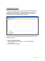
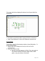
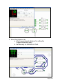
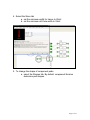
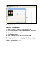
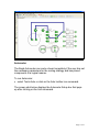
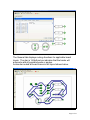
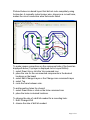
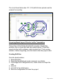
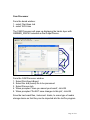
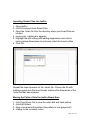
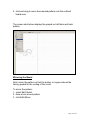
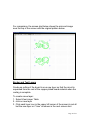
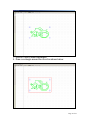
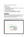
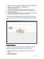
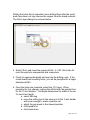
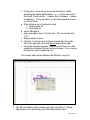
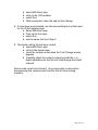
PCB Design and Fabrication
Quick Start Guide
This tutorial describes the processes involved in producing a single
layer PCB.
Note: Any Eagle CAD instructions listed within the tutorial are
executable using tool bar script box by entering the name of the
command icon and pressing enter.
Creating a Board From a Schematic
1. Create a schematic using Eagle Schematic.
2. Click on the “Board” icon when the schematic is complete. This
opens up Layout Editor and creates a board file with the same
name as that of the schematic.
Page 1 of 21
Creating a Board Layout
In the screen shot below, the circuit components and “ratsnest” are
on the left side of the window. Eagle uses the term, airwires, to
describe the rubber band-like connections between components.
The black frame represents the board outlines.
Create the circuit design within the board area using the Move and
Rotate commands.
To display component names:
1. select View>Display/hide layers….or click on the Display
command icon
2. click on layer 25 (tNames).
Page 2 of 21
The screen shot below displays the desired circuit layout within the
board area.
To calculate the shortest possible component airwire connections:
• select Tools>Ratsnest or click on the Ratsnest command icon
Design Rules
Design Rules specify all parameters relative to board fabrication. To
access Design Rules:
1. Select Tools >Drc (Design rule check) or click on the Drc
command icon.
2. Select the Clearance tab.
a. Set Wire and Pad clearance to 20mil. This value refers to
the minimum distance between copper traces, solder
pads, or any vias (holes) in the board.
Page 3 of 21
3. Select the Distance tab
a. 60mil is an adequate distance for setting the
Copper/Demension entry.
b. Set the entry for Drill/Hole to 75mil.
Page 4 of 21
4. Select the Sizes tab
a. set the minimum width for traces to 20mil
b. set the minimum drill hole width to 32mil
5. To change the shape of component pads:
a. select the Shapes tab. By default, component libraries
determine pad shapes.
Page 5 of 21
Routing the Board
Placing the Tracks Manually
1. select Edit>Route or click on the Route command icon.
2. click on component pads or airwires and make track connections.
To change track direction or orientation
1. click at the desired point
2. select the appropriate Wire bend icon from the toolbar
The screen shot below shows routing connections from the positive
lead of C1 to R2 and pins 2 and 6 of IC1. The negative lead of C1 is
routed to LSP2 and to pin 1 of IC1.
Page 6 of 21
Autorouter
The Eagle Autorouter can route a board completely if the user has set
the necessary parameters for the routing strategy and has placed
components in a logical manner.
To run Autorouter:
• select Tools>Auto or click on the Auto toolbar icon command.
The screen shot below displays the Autorouter Setup box that pops
up after clicking on the Auto command.
Page 7 of 21
The General tab displays routing directions for applicable board
layers. The star in 16 Bottom box indicates that the tracks will
autoroute with all possible bends or angles.
Autorouter routed all board traces in the layout shown below.
Page 8 of 21
Pictured below is a board layout that did not route completely using
Autorouter. A manually routed jumper wire, shown as a curved trace,
makes the circuit connection were Autorouter failed.
To make jumper connections on the component side of the board as
displayed above (Top layer is displayed red in Layout Editor):
1. select Draw>Via or click the Via command icon
2. place the vias for the unconnected components in the desired
locations on the board
3. select Edti>Change>Layer or the Change icon command>Layer
4. select Top
5. route the trace between vias.
To add mounting holes for a board:
1. select Draw>Hole or click on the Hole command icon
2. place the holes in desired locations.
To change the size of a drill bit needed for a mounting hole:
1. Edit> Change>Drill
2. choose the size of drill bit needed.
Page 9 of 21
The circuit board below has 1/8” (.125) drill bit holes placed near the
corners for mounting.
Preparing Board Layout Files for IsoPro Transalation
This section of the tutorial describes the process of preparing
definition files for board drill and track specifications. These files
import into the IsoPro software, which controls the T-Tech routing
machine. Before beginning, save the board under the project name.
Creating Drill files
From the board window:
1. Select File>Run
2. Select the file drillcfg.ulp (script command: run drillcfg)
3. In the Eagle Drill Configuration box, check inches for output file
units
4. click OK
5. click OK for the drill bit sizes
6. Save the configuration file under the project
Page 10 of 21
Cam Processor
From the board window:
1. select File>Open Job
2. select WCU.cam
The CAM Processor will open up displaying the tracks layer with
GERBER_RS274X selected as the Output Device.
From the CAM Processor window
1. Select File>Open>Board
2. Select the .brd (board) file to be processed
3. Select Process Job
4. When prompted “Have you saved your board”, click OK
5. When prompted “Do NOT save changes to this job”, click OK
Save the two board files, .holes and .tracks, to some type of media
storage device so that they can be imported into the IsoPro program.
Page 11 of 21
Importing Gerber Files into IsoPro
1. Open IsoPro
2. click File>Import>Auto Detect Files
3. Open the .holes file from the directory where your board files are
located.
4. press enter, a dialog box appears.
5. Highlight the drill setting with leading suppression and units in
inches whose dimensions most closely match the board outline.
6. Click OK.
Repeat the import process for the .tracks file. Choose the file with
leading suppression that most closely matches the dimensions of the
.holes file that was imported.
Moving the Pattern Onto the IsoPro Board Area
1.
2.
3.
4.
click View>Zoom Out to view the entire drill and track pattern
click Edit>Select
drag a box around the pattern (the pattern is now grayed out)
change to the crosshair cursor
Page 12 of 21
5. click and drag to move the selected pattern onto the outlined
board area.
The screen shot below displays the grayed out drill hole and track
pattern.
Mirroring the Board
Next, mirror the pattern so that the bottom or copper side will be
facing upward for the routing of the circuit.
To mirror the pattern:
1. select Edit>Select
2. draw a box around pattern
3. click Edit>Mirror
Page 13 of 21
For comparison, the screen shot below shows the mirrored image
near the top of the screen with the original pattern below.
Border and Text Layers
Create an outline of the board is on a new layer so that the circuit is
separated from the rest of the copper plated board material when the
routing is complete.
To create a new layer:
1. Select View>Layer Table
2. click on new layer
3. Click each layer icon in the upper left corner of the screen to set all
but the new layer on “View” as shown in the next screen shot.
Page 14 of 21
1. click on Tools>Create Rectangles
2. Draw a rectangle around the circuit as shown below:
Page 15 of 21
Text may be added to the design, if desired.
To add text:
1. View>Layer Table
2. click on new layer.
3. Click each layer icon in the upper left corner of the screen and set
all but the new layer on “View”.
4. select Tools>Create Text
5. enter the desired text in the text box
6. set the text size to .05 (inches) with vector font selected
7. place the text in an appropriate location on the board
Track Isolations
Isolations create an outline around the pads and tracks of the design
so that the T-Tech routing machine can route the board. This
process typically uses two isolations. IsoPro will produce a single
isolation for tracks too close for two passes in.
1. Click Tools>Isolate, and observe the dialog box as shown below.
Page 16 of 21
2. Select the layer that needs to be isolated
3. Choosing the appropriate isolation widths and passes. The default
settings of .010” and .020” should be sufficient for hand-soldered
boards.
4. click Isolate
The screen shot below displays the circuit tacks with 10 and 20 mil
isolations.
Board Placement
It is very important for proper board placement before beginning the
routing process. The small circle midway between the top and
bottom board edges and close (3 X’s over) to the left edge represents
the actual dowel pin holding the copper plate in place on the Quick
Circuit routing machine.
Note: the Quick Circuit router has built in limit switches that prevent
routing within .5 inches from the edge of the copper plate.
To position the board for routing:
1. Find an open location on the copper board plate
Page 17 of 21
2. Measure, from the closest edges of the copper plate, the X and Y
position of the circuit border (see Note above).
3. Change all layers to edit
4. Select the circuit board and move it close to the area that
corresponds to the copper plate measurements taken in step 2.
5. Select Tool>Measure
6. Use the measuring tool to determine the actual X and Y distances
of the board’s placement in relation to the borders.
The screen shot below displays the measuring tool’s X dimension
from the circuit border to that of the border representing the copper
plate.
Routing the board:
Graphical descriptions of the tools used in routing the board are
displayed on page 26 of the Quick Circuit User’s Manual.
1. Click on Mill>Initialize to prepare the machine for routing the
board.
2. Click Mill>Run Layer
3. select the drill layer
Page 18 of 21
Drilling the holes first is important, since drilling them after the small
pads have been cut may remove the copper from the board material.
The Run Layer dialog box is shown below.
4. Select “Run” and insert the proper drill bit. A .032” drill is fine for
most through-hole components and connectors.
5. Check for appropriate depth and execute the drilling cycle. If the
circuit board has mounting holes, you will be prompted for a larger
diameter drill bit.
6. Once the holes are complete, select the .010 layer. When
prompted for tool change, replace the drill bit with the pointed tool
for the 10 mil isolation. Tool depth determines the width of the cut.
To check tool depth:
a. select Mill>Jog
b. move the milling tool to the area next to the Y-axis border
with room enough to make a practice cut
c. adjust the jog speed to the slowest position
d. click spindle on
e. click head down
Page 19 of 21
f. clicking the Y-axis arrow, move the milling tool while
adjusting the depth adjustment (+ or -) on the solenoid of
the Quick Circuit router. + makes the cut deeper, - makes
it shallower. It may be easier to use the keyboard arrows
for this function.
g. After milling a cut of at least an inch
i. click spindle off
ii. click head up
h. select Mill>Move
i. when prompted, type 10 in the box. This moves the mill
.010”
j. Repeat steps d and e
k. click the Y-axis arrow or keyboard arrow and move the
mill in the opposite direction-do not adjust the depth
l. using the magnifying glass, check to see if there is a thin
copper line between the two cuts just made. If not, repeat
the process with a shallower cut.
The screen shot below displays the Machine Jog tool.
7. The 20 mil isolation layer routes using the end mil tool. Depth
adjustment is not necessary with the milling of this layer.
Page 20 of 21
a.
b.
c.
d.
select Mill>Run Layer
click on the .020 isolation
select Run
When prompted, make the end mil tool change.
8. If a text layer was included, use the same milling tool as that used
for the 20 mil isolation layer.
a. Select Mill>Run Layer
b. Click on the text layer
c. select Run
d. use the same tool as in Step 6
9. The border will be the last layer routed.
a. select Mill>Run Layer
b. click on the border layer
c. Insert the contour router when the Tool Change prompt
appears.
d. Carefully adjust the contour routing tool with the + or –
depth adjustment so that the tool cuts through the board
material.
Remove the routed circuit board. Any excess dust is removed by
disconnecting the vacuum hose from the Quick Circuit routing
machine.
Page 21 of 21